Embed Size (px)
Citation preview
Introduction to Lab & Homework
Kun-Bin Lee 李坤儐李坤儐李坤儐李坤儐
Oct. 29, 2001
Department of Electronics EngineeringNational Chiao Tung University
1/30
Institute of Electronics, National C
hiao Tung U
niversityIntroduction to Lab &
Hom
ework
Outline
• System-Level Design and Modeling• IP Core Design• Lab & Homework
2/30
Institute of Electronics, National C
hiao Tung U
niversityIntroduction to Lab &
Hom
ework
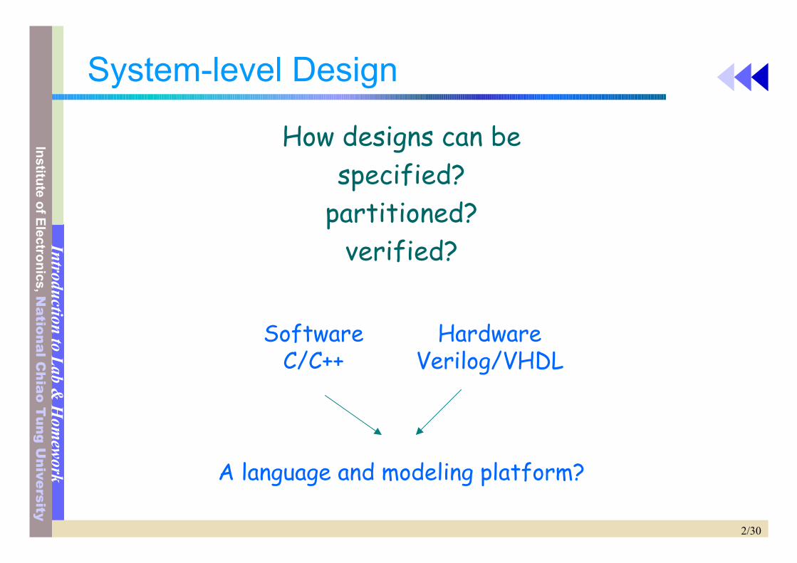
System-level Design
How designs can bespecified?
partitioned?verified?
SoftwareC/C++
HardwareVerilog/VHDL
A language and modeling platform?
3/30
Institute of Electronics, National C
hiao Tung U
niversityIntroduction to Lab &
Hom
ework
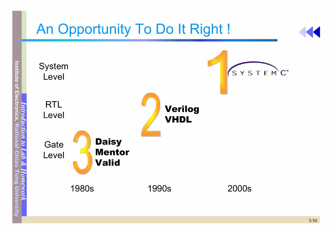
An Opportunity To Do It Right !
4/30
Institute of Electronics, National C
hiao Tung U
niversityIntroduction to Lab &
Hom
ework
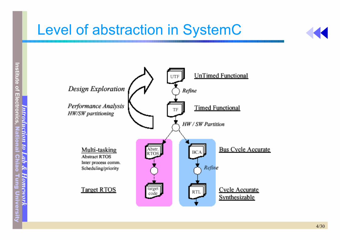
Level of abstraction in SystemC
5/30
Institute of Electronics, National C
hiao Tung U
niversityIntroduction to Lab &
Hom
ework
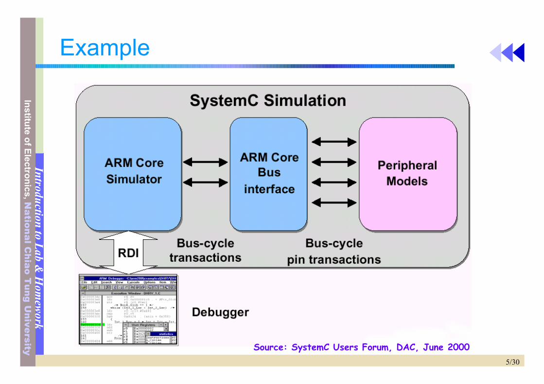
Example
Source: SystemC Users Forum, DAC, June 2000
6/30
Institute of Electronics, National C
hiao Tung U
niversityIntroduction to Lab &
Hom
ework
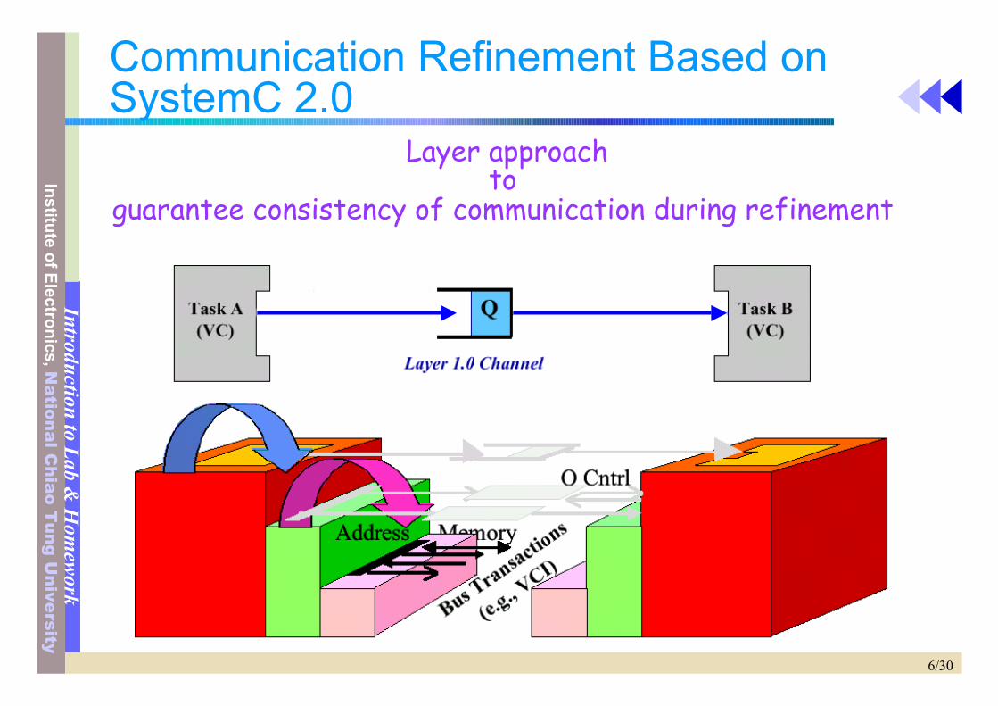
Communication Refinement Based onSystemC 2.0
Layer approachto
guarantee consistency of communication during refinement
7/30
Institute of Electronics, National C
hiao Tung U
niversityIntroduction to Lab &
Hom
ework
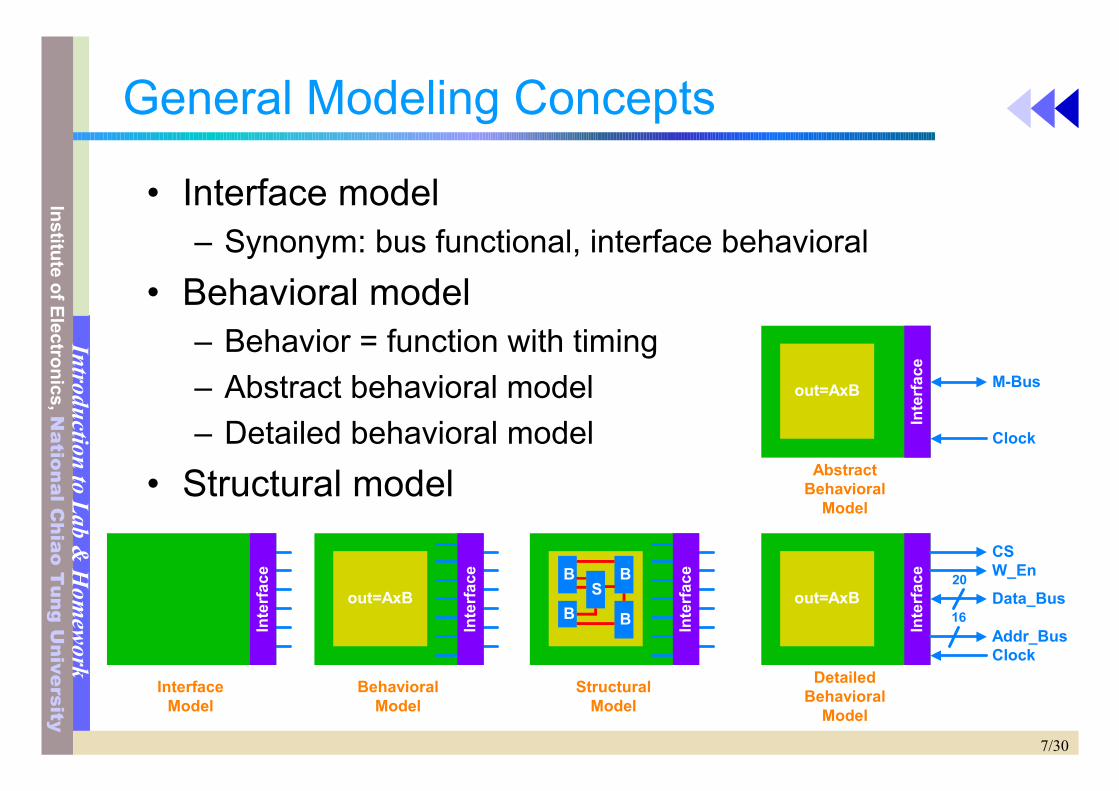
General Modeling Concepts
• Interface model– Synonym: bus functional, interface behavioral
• Behavioral model– Behavior = function with timing– Abstract behavioral model– Detailed behavioral model
• Structural model
BehavioralModel
out=AxB
Inte
rface
StructuralModel
Inte
rfaceB
B
B
B
S
Clock
M-Bus
AbstractBehavioral
Model
out=AxB
Inte
rface
DetailedBehavioral
Model
out=AxB
Inte
rface
Data_Bus
Addr_BusClock
16
20 W_EnCS
InterfaceModel
Inte
rface
8/30
Institute of Electronics, National C
hiao Tung U
niversityIntroduction to Lab &
Hom
ework
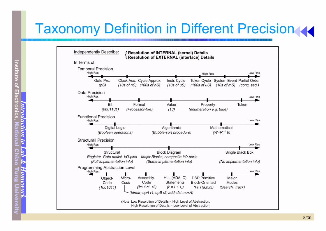
Taxonomy Definition in Different Precision
9/30
Institute of Electronics, National C
hiao Tung U
niversityIntroduction to Lab &
Hom
ework
The Intent of Different Level of IP Model
• Design exploration at higher level– Import of top-level constraint and block architecture– Hierarchical, complete system refinement– Less time for validating system requirement– More design space of algorithm and system
architecture• Simple and efficient verification and simulation
– Functional verification– Timing simulation/verification– Separate internal and external (interface) verification– Analysis: power and timing
• Verification support
10/30
Institute of Electronics, National C
hiao Tung U
niversityIntroduction to Lab &
Hom
ework
Issues of IP Modeling
• Attributes– What is a sufficient set of model attributes?– How are these model attributes validated?– How is the proper application of an abstract model
specified?• Two important dimensions of time
– Model development time is labor intensive: modelreusability
– Simulation time depends upon strategy chosen formixed domain simulations
11/30
Institute of Electronics, National C
hiao Tung U
niversityIntroduction to Lab &
Hom
ework
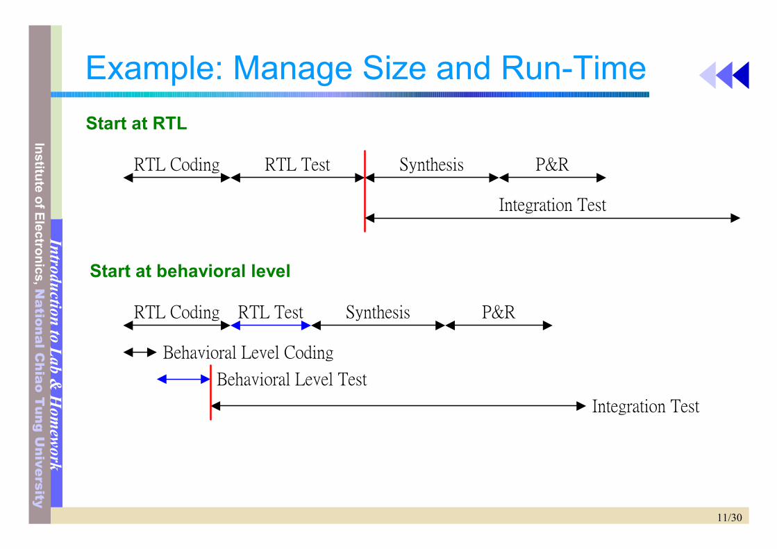
Example: Manage Size and Run-Time
RTL Coding RTL Test Synthesis
Integration Test
RTL Coding RTL Test Synthesis
Behavioral Level Coding
Behavioral Level Test
P&R
P&R
Integration Test
Start at RTL
Start at behavioral level
12/30
Institute of Electronics, National C
hiao Tung U
niversityIntroduction to Lab &
Hom
ework
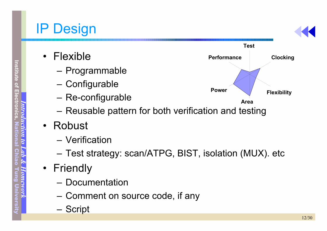
IP Design
• Flexible– Programmable– Configurable– Re-configurable– Reusable pattern for both verification and testing
• Robust– Verification– Test strategy: scan/ATPG, BIST, isolation (MUX). etc
• Friendly– Documentation– Comment on source code, if any– Script
Power
AreaFlexibility
Test
Performance Clocking
13/30
Institute of Electronics, National C
hiao Tung U
niversityIntroduction to Lab &
Hom
ework
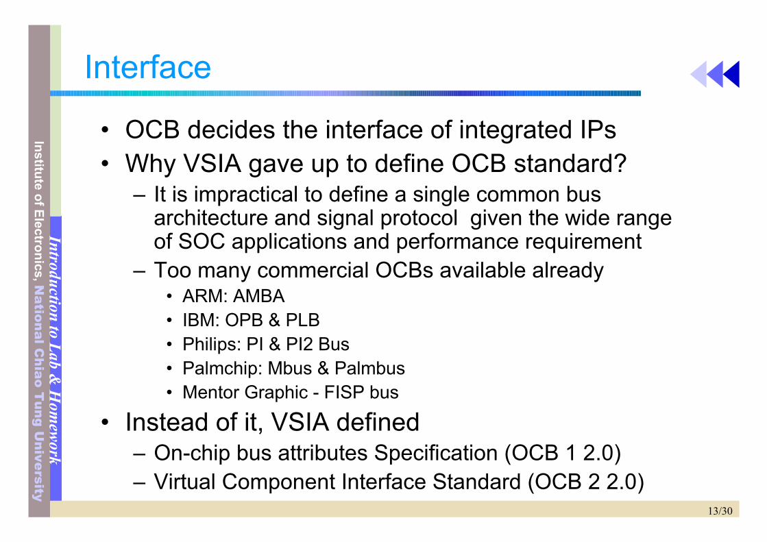
Interface
• OCB decides the interface of integrated IPs• Why VSIA gave up to define OCB standard?
– It is impractical to define a single common busarchitecture and signal protocol given the wide rangeof SOC applications and performance requirement
– Too many commercial OCBs available already• ARM: AMBA• IBM: OPB & PLB• Philips: PI & PI2 Bus• Palmchip: Mbus & Palmbus• Mentor Graphic - FISP bus
• Instead of it, VSIA defined– On-chip bus attributes Specification (OCB 1 2.0)– Virtual Component Interface Standard (OCB 2 2.0)
14/30
Institute of Electronics, National C
hiao Tung U
niversityIntroduction to Lab &
Hom
ework
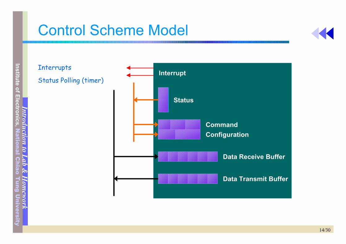
Control Scheme Model
Status
CommandConfiguration
Data Receive Buffer
Data Transmit Buffer
InterruptInterrupts
Status Polling (timer)
15/30
Institute of Electronics, National C
hiao Tung U
niversityIntroduction to Lab &
Hom
ework
OCB De Facto Standard - AMBA
• ARM dominated 70% of embedded processormarket– AMBA 2.0 is adopted by a lot of companies, including
Synopsys, Samsung, ARC, inSilicon, MIPS, etc– E.g., AMBA-based DesignWare IP
• AMBA is open and free– you have to license it from ARM and ARM owns patent
on it• AMBA Design Kit (ADK) and AMBA Compliance
Testbench (ACT) are available from ARM• Multi-layer AHB is define by ARM from complex
multi-master system
16/30
Institute of Electronics, National C
hiao Tung U
niversityIntroduction to Lab &
Hom
ework
VSIA VCI
• Some vendors are developing VCI wrappergenerator
• Some vendors begin to provide VCI-AMBAwrapper
• Some vendors begin to provide design with VCIinterface
17/30
Institute of Electronics, National C
hiao Tung U
niversityIntroduction to Lab &
Hom
ework
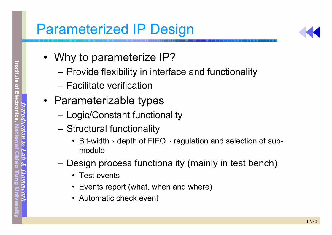
Parameterized IP Design
• Why to parameterize IP?– Provide flexibility in interface and functionality– Facilitate verification
• Parameterizable types– Logic/Constant functionality– Structural functionality
• Bit-width、depth of FIFO、regulation and selection of sub-module
– Design process functionality (mainly in test bench)• Test events• Events report (what, when and where)• Automatic check event
18/30
Institute of Electronics, National C
hiao Tung U
niversityIntroduction to Lab &
Hom
ework
Verification
• Function• Architecture functional verification• Control algorithm and protocol verification• Hardware RTL verification• hardware and software interface certification (via
HW-SW Co-sim)• Hardware and software coverification (via rapid
prototyping)• Netlist verification
19/30
Institute of Electronics, National C
hiao Tung U
niversityIntroduction to Lab &
Hom
ework
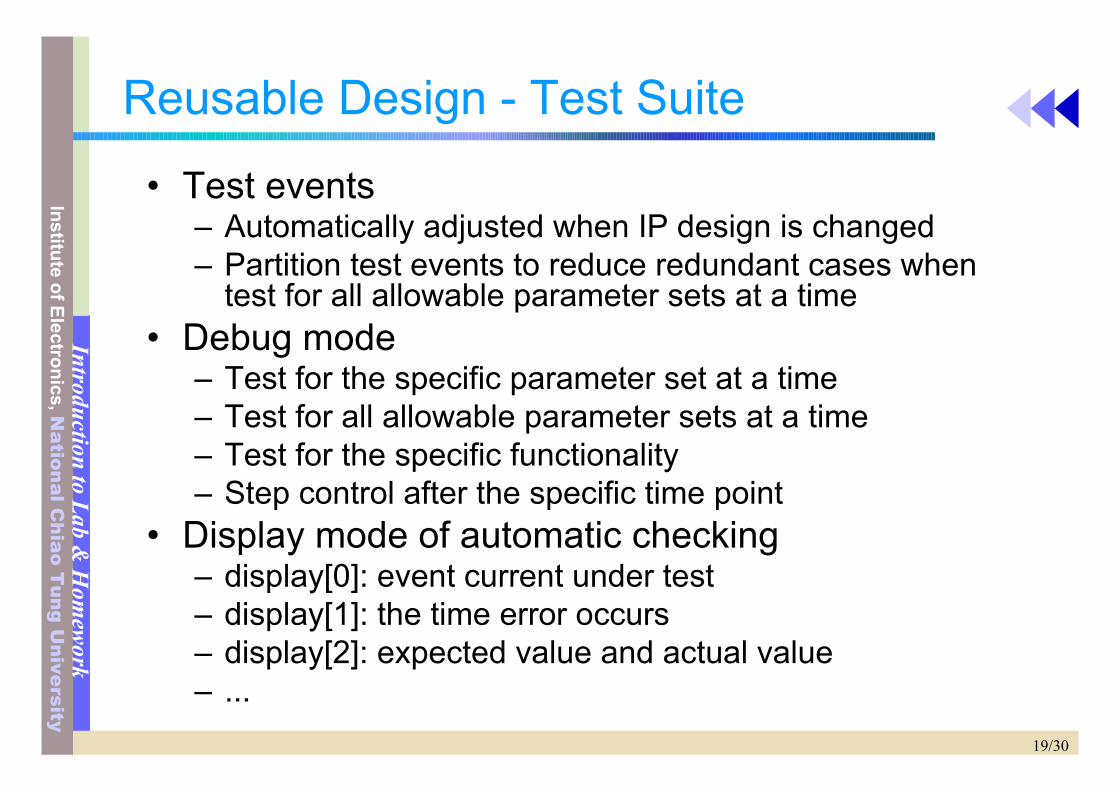
Reusable Design - Test Suite
• Test events– Automatically adjusted when IP design is changed– Partition test events to reduce redundant cases when
test for all allowable parameter sets at a time• Debug mode
– Test for the specific parameter set at a time– Test for all allowable parameter sets at a time– Test for the specific functionality– Step control after the specific time point
• Display mode of automatic checking– display[0]: event current under test– display[1]: the time error occurs– display[2]: expected value and actual value– ...
20/30
Institute of Electronics, National C
hiao Tung U
niversityIntroduction to Lab &
Hom
ework
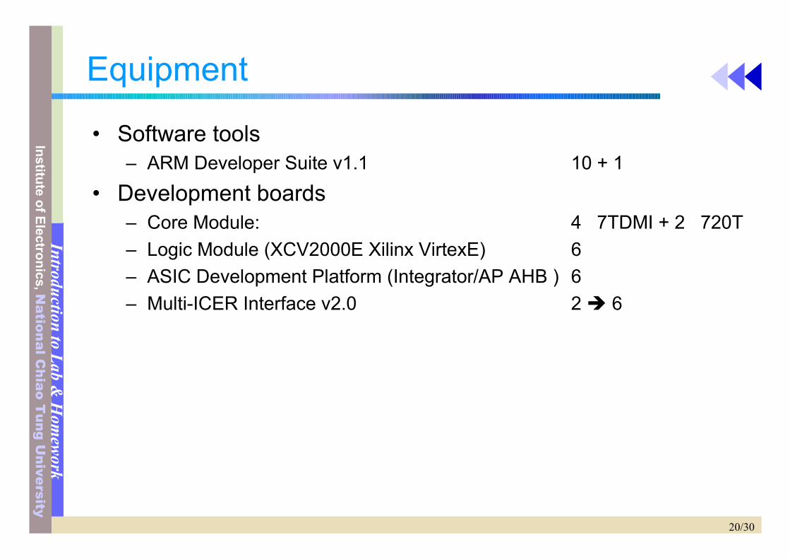
Equipment
• Software tools– ARM Developer Suite v1.1
• Development boards– Core Module:– Logic Module (XCV2000E Xilinx VirtexE)– ASIC Development Platform (Integrator/AP AHB )– Multi-ICER Interface v2.0
10 + 1
4 7TDMI + 2 720T662 6
21/30
Institute of Electronics, National C
hiao Tung U
niversityIntroduction to Lab &
Hom
ework
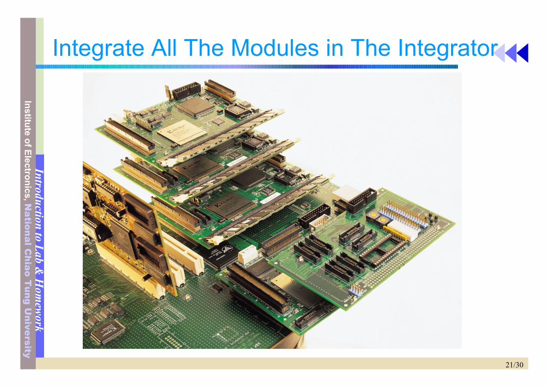
Integrate All The Modules in The Integrator
22/30
Institute of Electronics, National C
hiao Tung U
niversityIntroduction to Lab &
Hom
ework
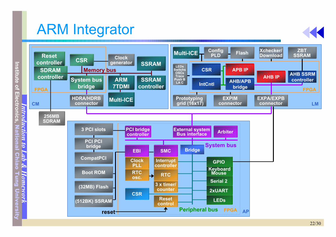
ARM Integrator
System bus
GPIO Keyboard
Mouse Serial 2
2xUART
LEDs
ClockPLLRTCosc.
CSR
Interruptcontroller
RTC
3 x timer/counter
Resetcontrol
Bridge
PCI bridgecontroller
Peripheral bus
SMC
reset
3 PCI slots
PCI PCIbridge
CompatPCIEBI
ArbiterExternal systemBus interface
Boot ROM
(32MB) Flash
(512BK) SSRAM
256MBSDRAM
ARM7TDMI
Multi-ICE
SSRAM
SSRAMcontroller
Memory busSystem bus
bridge
SDRAMcontroller
CSRReset
controller
HDRA/HDRBconnector
Clockgenerator
ZBTSSRAMFlash
AHB SSRMcontrollerAHB/APB
bridge
CSR
IntCntl
APB IPAHB IP
Multi-ICE ConfigPLD
Xchecker/Download
EXPA/EXPBconnector
EXPIMconnector
Prototyping grid (16x17)
FPGA FPGA
FPGA
LEDsSwitchsOSCsTrace
Push BLA C
CM
AP
LM
23/30
Institute of Electronics, National C
hiao Tung U
niversityIntroduction to Lab &
Hom
ework
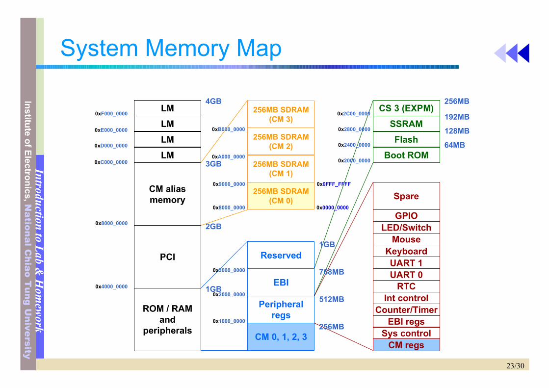
System Memory Map
ROM / RAMand
peripherals
PCI
CM aliasmemory
1GB
2GB
3GB
4GB
LMLMLMLM
0xC000_0000
0xD000_0000
0xE000_0000
0xF000_0000 256MB SDRAM(CM 3)
256MB SDRAM(CM 2)
256MB SDRAM(CM 1)
256MB SDRAM(CM 0) Spare
GPIOLED/Switch
MouseKeyboardUART 1UART 0
RTCInt control
Counter/TimerEBI regs
Sys controlCM regs
Reserved
EBI
Peripheralregs
CM 0, 1, 2, 3
CS 3 (EXPM)SSRAMFlash
Boot ROM
256MB
512MB
768MB
1GB
64MB
128MB
192MB
256MB
0x9000_0000
0xA000_0000
0x8000_0000
0xB000_0000
0x0FFF_FFFF
0x0000_0000
0x2000_0000
0x2400_0000
0x2800_0000
0x2C00_0000
0x8000_0000
0x4000_0000
0x1000_0000
0x2000_0000
0x3000_0000
24/30
Institute of Electronics, National C
hiao Tung U
niversityIntroduction to Lab &
Hom
ework
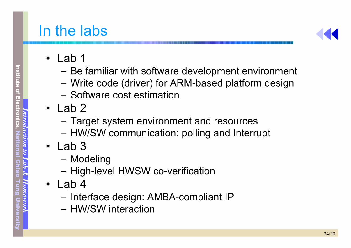
In the labs
• Lab 1– Be familiar with software development environment– Write code (driver) for ARM-based platform design– Software cost estimation
• Lab 2– Target system environment and resources– HW/SW communication: polling and Interrupt
• Lab 3– Modeling– High-level HWSW co-verification
• Lab 4– Interface design: AMBA-compliant IP– HW/SW interaction
25/30
Institute of Electronics, National C
hiao Tung U
niversityIntroduction to Lab &
Hom
ework
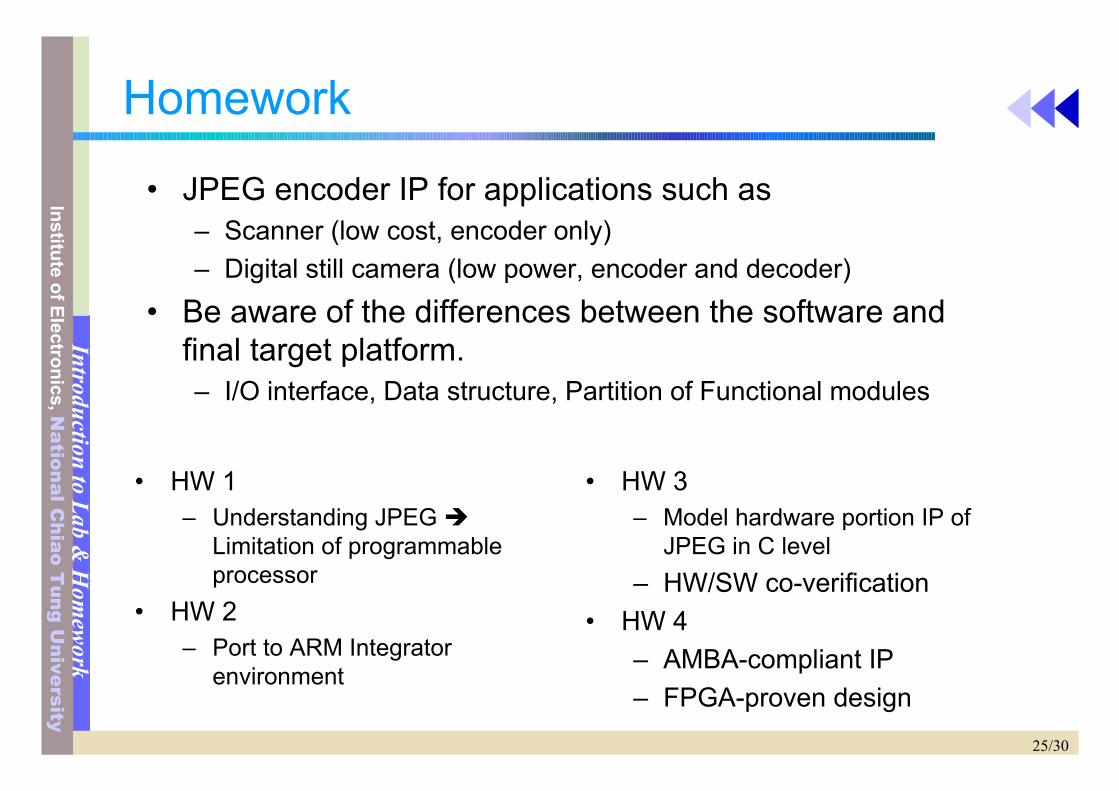
Homework
• JPEG encoder IP for applications such as– Scanner (low cost, encoder only)– Digital still camera (low power, encoder and decoder)
• Be aware of the differences between the software andfinal target platform.– I/O interface, Data structure, Partition of Functional modules
• HW 1– Understanding JPEG
Limitation of programmableprocessor
• HW 2– Port to ARM Integrator
environment
• HW 3– Model hardware portion IP of
JPEG in C level– HW/SW co-verification
• HW 4– AMBA-compliant IP– FPGA-proven design
26/30
Institute of Electronics, National C
hiao Tung U
niversityIntroduction to Lab &
Hom
ework
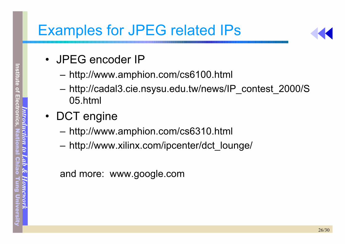
Examples for JPEG related IPs
• JPEG encoder IP– http://www.amphion.com/cs6100.html– http://cadal3.cie.nsysu.edu.tw/news/IP_contest_2000/S
05.html• DCT engine
– http://www.amphion.com/cs6310.html– http://www.xilinx.com/ipcenter/dct_lounge/
and more: www.google.com
27/30
Institute of Electronics, National C
hiao Tung U
niversityIntroduction to Lab &
Hom
ework
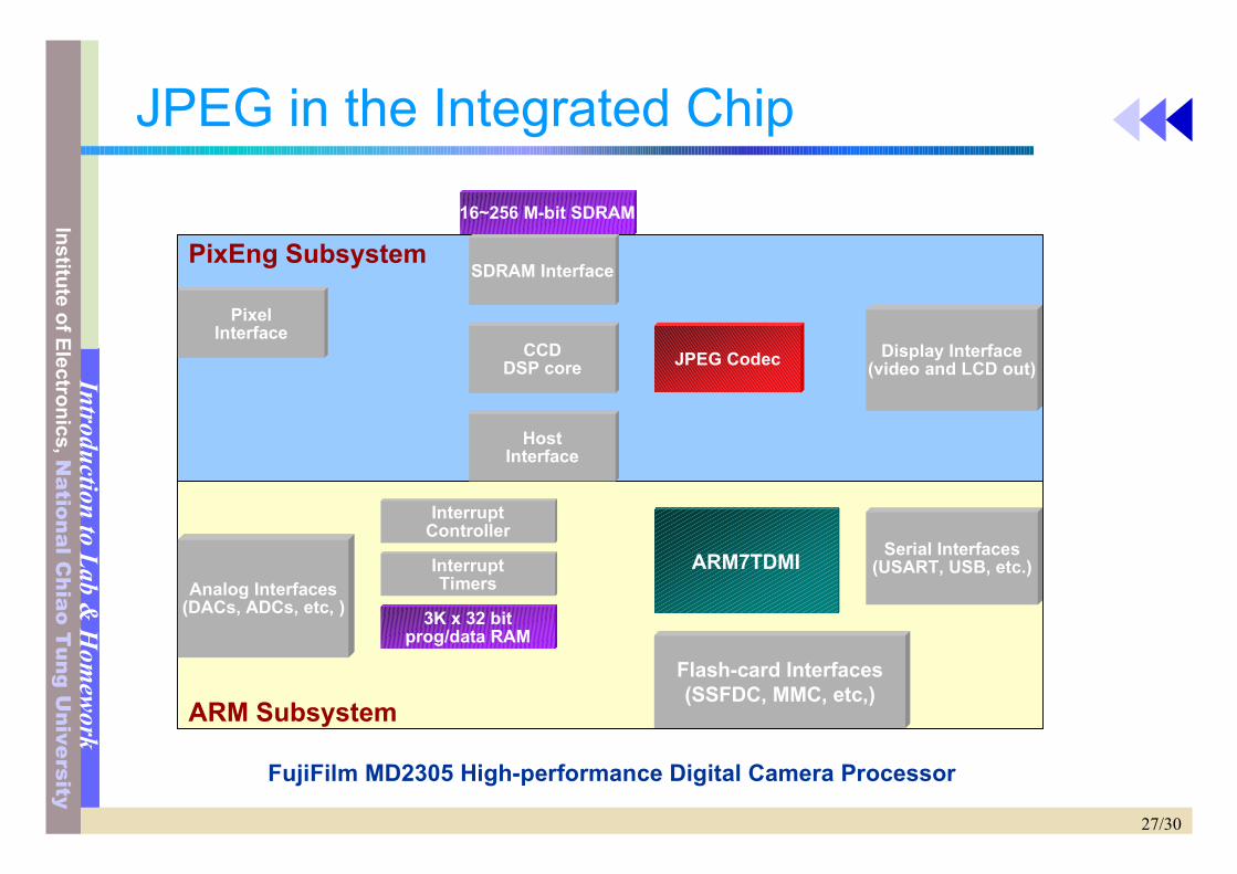
JPEG in the Integrated Chip
ARM7TDMI
CCDDSP core
Analog Interfaces(DACs, ADCs, etc, )
Display Interface(video and LCD out)
Serial Interfaces(USART, USB, etc.)
Flash-card Interfaces(SSFDC, MMC, etc,)
ARM Subsystem
FujiFilm MD2305 High-performance Digital Camera Processor
PixEng Subsystem
PixelInterface
SDRAM Interface
JPEG Codec
HostInterface
InterruptController
InterruptTimers
3K x 32 bitprog/data RAM
16~256 M-bit SDRAM
28/30
Institute of Electronics, National C
hiao Tung U
niversityIntroduction to Lab &
Hom
ework
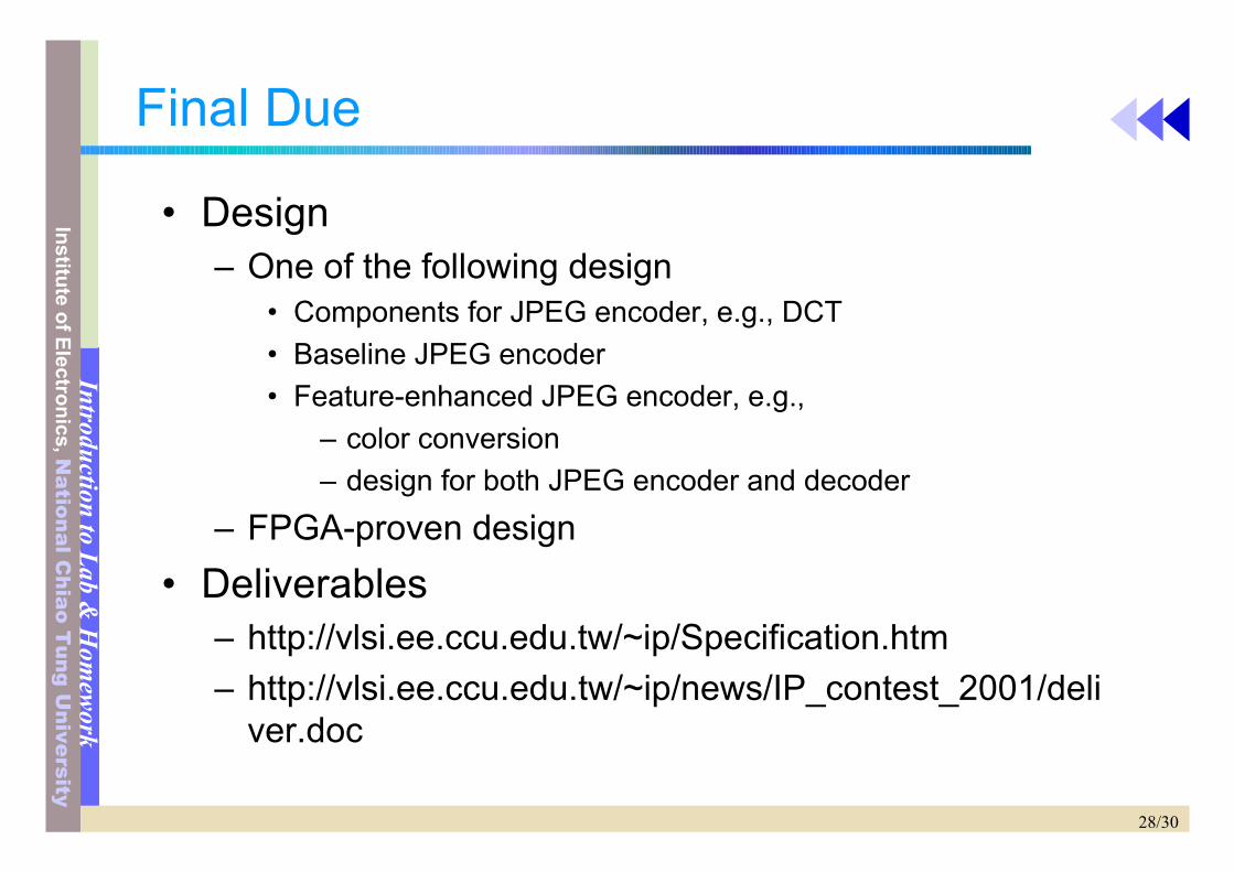
Final Due
• Design– One of the following design
• Components for JPEG encoder, e.g., DCT• Baseline JPEG encoder• Feature-enhanced JPEG encoder, e.g.,
– color conversion– design for both JPEG encoder and decoder
– FPGA-proven design• Deliverables
– http://vlsi.ee.ccu.edu.tw/~ip/Specification.htm– http://vlsi.ee.ccu.edu.tw/~ip/news/IP_contest_2001/deli
ver.doc
29/30
Institute of Electronics, National C
hiao Tung U
niversityIntroduction to Lab &
Hom
ework
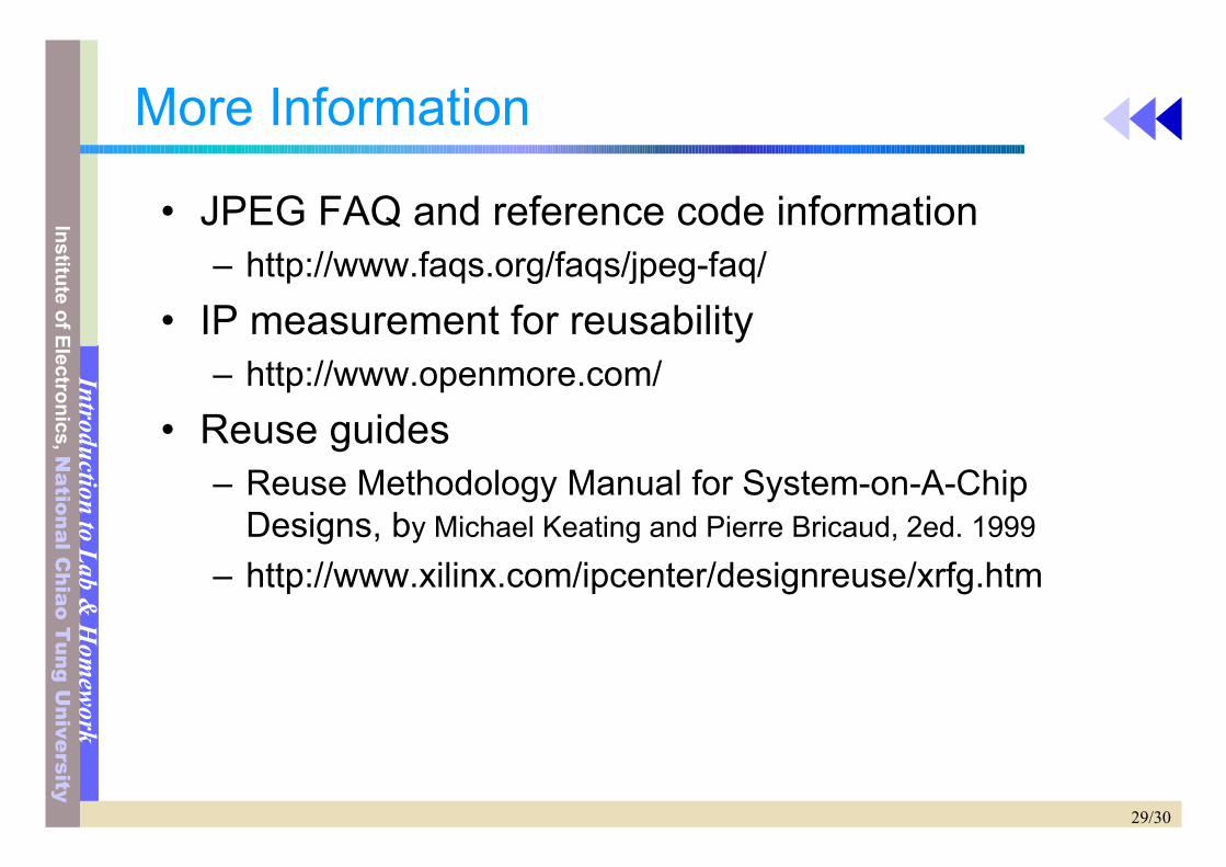
More Information
• JPEG FAQ and reference code information– http://www.faqs.org/faqs/jpeg-faq/
• IP measurement for reusability– http://www.openmore.com/
• Reuse guides– Reuse Methodology Manual for System-on-A-Chip
Designs, by Michael Keating and Pierre Bricaud, 2ed. 1999
– http://www.xilinx.com/ipcenter/designreuse/xrfg.htm
30/30
Institute of Electronics, National C
hiao Tung U
niversityIntroduction to Lab &
Hom
ework
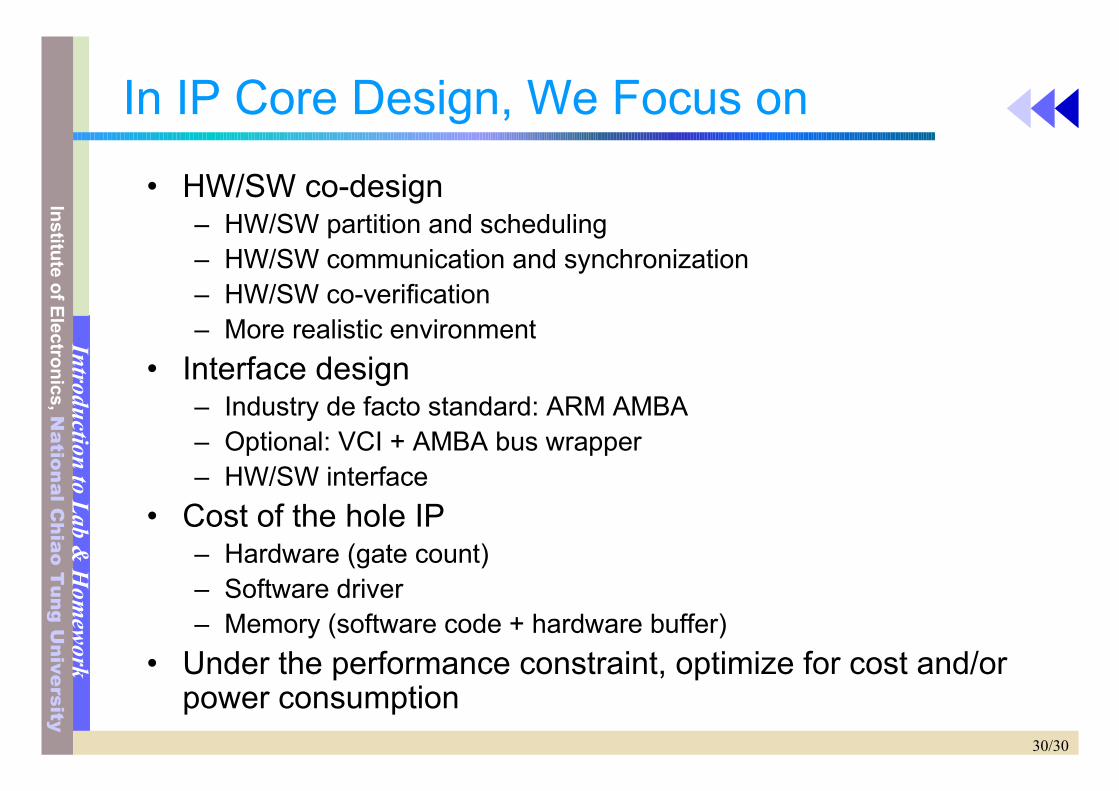
In IP Core Design, We Focus on
• HW/SW co-design– HW/SW partition and scheduling– HW/SW communication and synchronization– HW/SW co-verification– More realistic environment
• Interface design– Industry de facto standard: ARM AMBA– Optional: VCI + AMBA bus wrapper– HW/SW interface
• Cost of the hole IP– Hardware (gate count)– Software driver– Memory (software code + hardware buffer)
• Under the performance constraint, optimize for cost and/orpower consumption