Embed Size (px)
Citation preview
April 5, 1999 14:05 g02-ch2 Sheet number 1 Page number 17 black
17
c h a p t e r
2Introduction to Logic Circuits
2. d2–d4, d7–d5
April 5, 1999 14:05 g02-ch2 Sheet number 2 Page number 18 black
18 C H A P T E R 2 • Introduction to Logic Circuits
The study of logic circuits is motivated mostly by their use in digital computers. But such circuits also formthe foundation of many other digital systems where performing arithmetic operations on numbers is not ofprimary interest. For example, in a myriad of control applications actions are determined by some simplelogical operations on input information, without having to do extensive numerical computations.
Logic circuits perform operations on digital signals and are usually implemented as electronic circuitswhere the signal values are restricted to a few discrete values. Inbinary logic circuits there are only twovalues, 0 and 1. In decimallogic circuits there are 10 values, from 0 to 9. Since each signal value is naturallyrepresented by a digit, such logic circuits are referred to asdigital circuits. In contrast, there existanalogcircuits where the signals may take on a continuous range of values between some minimum and maximumlevels.
In this book we deal with binary circuits, which have the dominant role in digital technology. We hope toprovide the reader with an understanding of how these circuits work, how are they represented in mathematicalnotation, and how are they designed using modern design automation techniques. We begin by introducingsome basic concepts pertinent to the binary logic circuits.
2.1 Variables and Functions
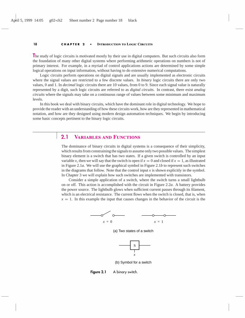
The dominance of binary circuits in digital systems is a consequence of their simplicity,which results from constraining the signals to assume only two possible values. The simplestbinary element is a switch that has two states. If a given switch is controlled by an inputvariablex, then we will say that the switch is open ifx = 0 and closed ifx = 1, as illustratedin Figure 2.1a. We will use the graphical symbol in Figure 2.1b to represent such switchesin the diagrams that follow. Note that the control inputx is shown explicitly in the symbol.In Chapter 3 we will explain how such switches are implemented with transistors.
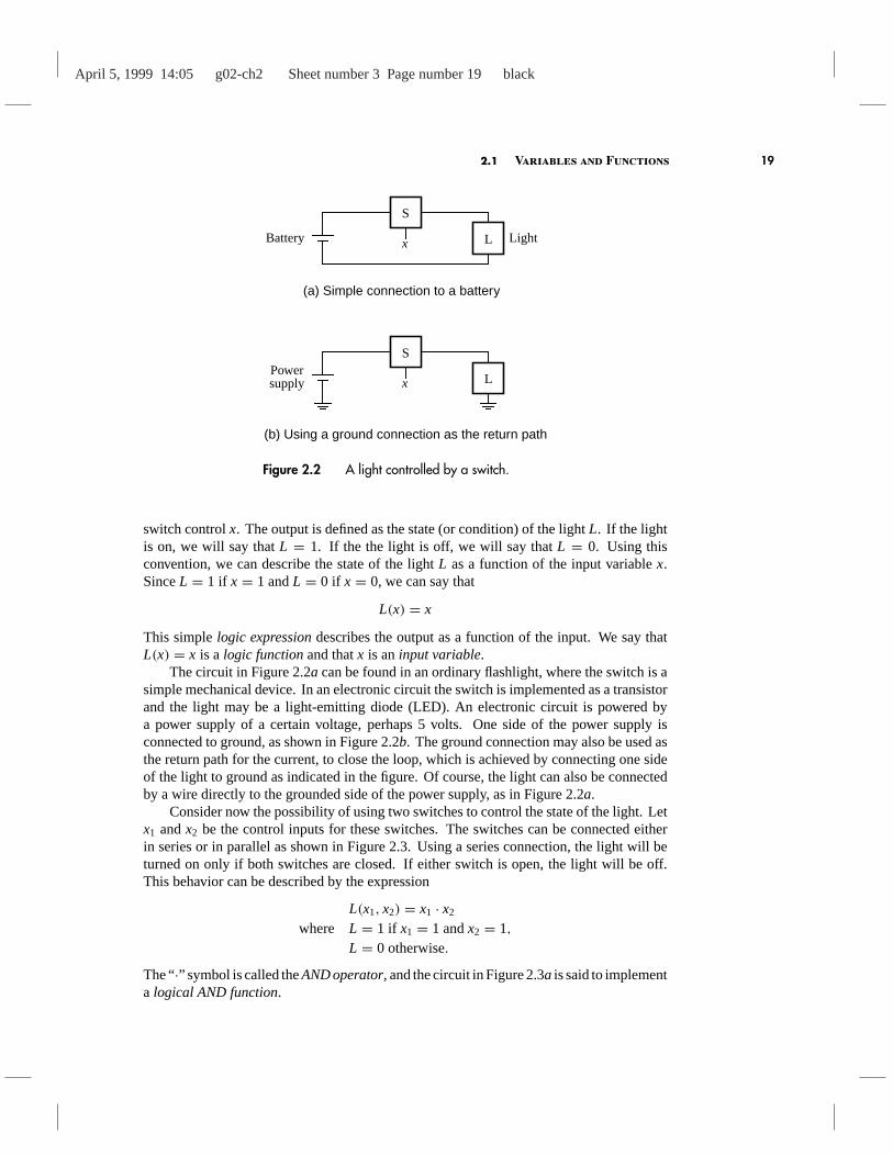
Consider a simple application of a switch, where the switch turns a small lightbulbon or off. This action is accomplished with the circuit in Figure 2.2a. A battery providesthe power source. The lightbulb glows when sufficient current passes through its filament,which is an electrical resistance. The current flows when the switch is closed, that is, whenx = 1. In this example the input that causes changes in the behavior of the circuit is the
x 1=x 0=
(a) Two states of a switch
S
x
(b) Symbol for a switch
Figure 2.1 A binary switch.
April 5, 1999 14:05 g02-ch2 Sheet number 3 Page number 19 black
2.1 Variables and Functions 19
(a) Simple connection to a battery
S
x
(b) Using a ground connection as the return path
LBattery Light
xPowersupply
S
L
Figure 2.2 A light controlled by a switch.
switch controlx. The output is defined as the state (or condition) of the lightL. If the lightis on, we will say thatL = 1. If the the light is off, we will say thatL = 0. Using thisconvention, we can describe the state of the lightL as a function of the input variablex.SinceL = 1 if x = 1 andL = 0 if x = 0, we can say that
L(x) = x
This simplelogic expressiondescribes the output as a function of the input. We say thatL(x) = x is a logic functionand thatx is aninput variable.
The circuit in Figure 2.2a can be found in an ordinary flashlight, where the switch is asimple mechanical device. In an electronic circuit the switch is implemented as a transistorand the light may be a light-emitting diode (LED). An electronic circuit is powered bya power supply of a certain voltage, perhaps 5 volts. One side of the power supply isconnected to ground, as shown in Figure 2.2b. The ground connection may also be used asthe return path for the current, to close the loop, which is achieved by connecting one sideof the light to ground as indicated in the figure. Of course, the light can also be connectedby a wire directly to the grounded side of the power supply, as in Figure 2.2a.
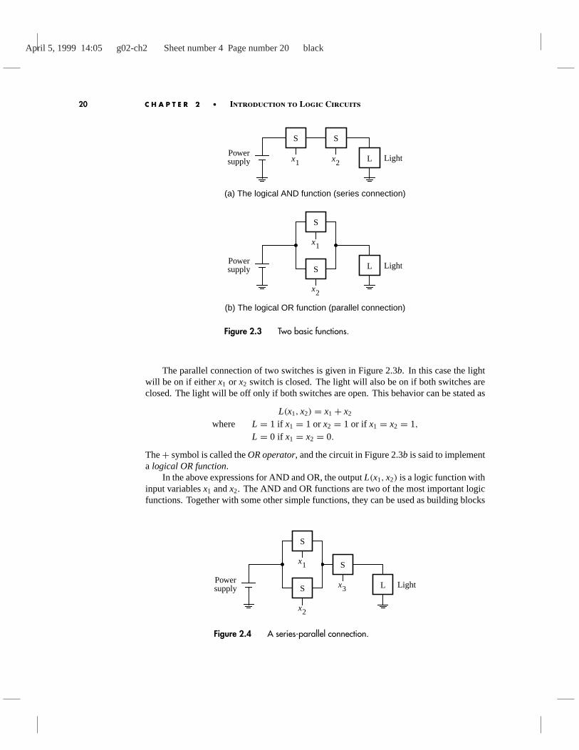
Consider now the possibility of using two switches to control the state of the light. Letx1 andx2 be the control inputs for these switches. The switches can be connected eitherin series or in parallel as shown in Figure 2.3. Using a series connection, the light will beturned on only if both switches are closed. If either switch is open, the light will be off.This behavior can be described by the expression
L(x1, x2) = x1 · x2
where L = 1 if x1 = 1 andx2 = 1,L = 0 otherwise.
The “·” symbol is called theAND operator, and the circuit in Figure 2.3a is said to implementa logical AND function.
April 5, 1999 14:05 g02-ch2 Sheet number 4 Page number 20 black
20 C H A P T E R 2 • Introduction to Logic Circuits
(a) The logical AND function (series connection)
S
x1 LPowersupply
S
x2
S
x1
LPowersupply S
x2
(b) The logical OR function (parallel connection)
Light
Light
Figure 2.3 Two basic functions.
The parallel connection of two switches is given in Figure 2.3b. In this case the lightwill be on if eitherx1 or x2 switch is closed. The light will also be on if both switches areclosed. The light will be off only if both switches are open. This behavior can be stated as
L(x1, x2) = x1+ x2
where L = 1 if x1 = 1 orx2 = 1 or if x1 = x2 = 1,L = 0 if x1 = x2 = 0.
The+ symbol is called theOR operator, and the circuit in Figure 2.3b is said to implementa logical OR function.
In the above expressions for AND and OR, the outputL(x1, x2) is a logic function withinput variablesx1 andx2. The AND and OR functions are two of the most important logicfunctions. Together with some other simple functions, they can be used as building blocks
S
x1
LPowersupply S
x2
Light
S
x3
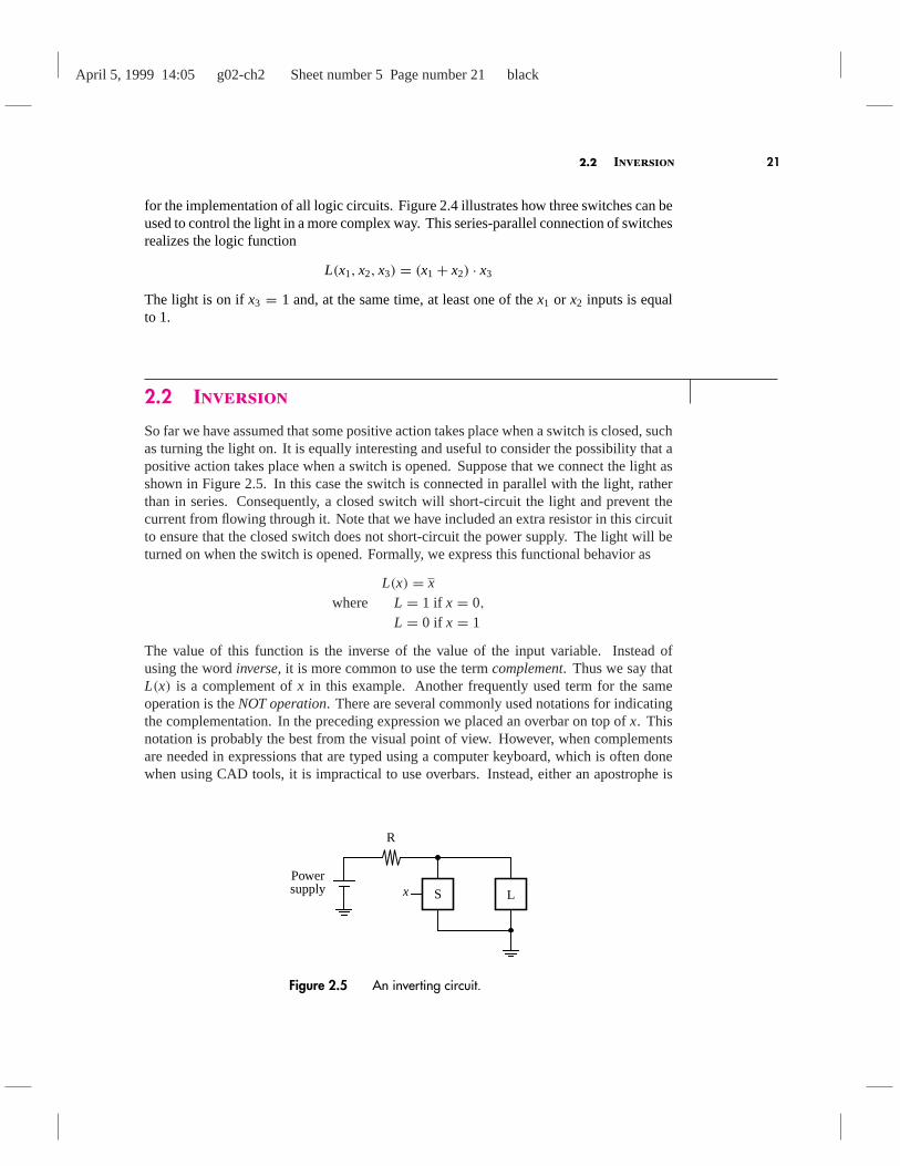
Figure 2.4 A series-parallel connection.
April 5, 1999 14:05 g02-ch2 Sheet number 5 Page number 21 black
2.2 Inversion 21
for the implementation of all logic circuits. Figure 2.4 illustrates how three switches can beused to control the light in a more complex way. This series-parallel connection of switchesrealizes the logic function
L(x1, x2, x3) = (x1+ x2) · x3
The light is on ifx3 = 1 and, at the same time, at least one of thex1 or x2 inputs is equalto 1.
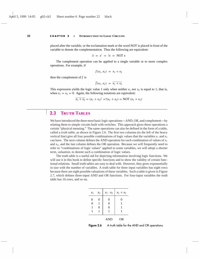
2.2 Inversion
So far we have assumed that some positive action takes place when a switch is closed, suchas turning the light on. It is equally interesting and useful to consider the possibility that apositive action takes place when a switch is opened. Suppose that we connect the light asshown in Figure 2.5. In this case the switch is connected in parallel with the light, ratherthan in series. Consequently, a closed switch will short-circuit the light and prevent thecurrent from flowing through it. Note that we have included an extra resistor in this circuitto ensure that the closed switch does not short-circuit the power supply. The light will beturned on when the switch is opened. Formally, we express this functional behavior as
L(x) = xwhere L = 1 if x = 0,
L = 0 if x = 1
The value of this function is the inverse of the value of the input variable. Instead ofusing the wordinverse, it is more common to use the termcomplement. Thus we say thatL(x) is a complement ofx in this example. Another frequently used term for the sameoperation is theNOT operation. There are several commonly used notations for indicatingthe complementation. In the preceding expression we placed an overbar on top ofx. Thisnotation is probably the best from the visual point of view. However, when complementsare needed in expressions that are typed using a computer keyboard, which is often donewhen using CAD tools, it is impractical to use overbars. Instead, either an apostrophe is
Sx L
Powersupply
R
Figure 2.5 An inverting circuit.
April 5, 1999 14:05 g02-ch2 Sheet number 6 Page number 22 black
22 C H A P T E R 2 • Introduction to Logic Circuits
placed after the variable, or the exclamation mark or the word NOT is placed in front of thevariable to denote the complementation. Thus the following are equivalent:
x = x′ = !x = NOT x
The complement operation can be applied to a single variable or to more complexoperations. For example, if
f (x1, x2) = x1+ x2
then the complement off is
f (x1, x2) = x1+ x2
This expression yields the logic value 1 only when neitherx1 nor x2 is equal to 1, that is,whenx1 = x2 = 0. Again, the following notations are equivalent:
x1+ x2 = (x1+ x2)′ =!(x1+ x2) = NOT (x1+ x2)
2.3 Truth Tables
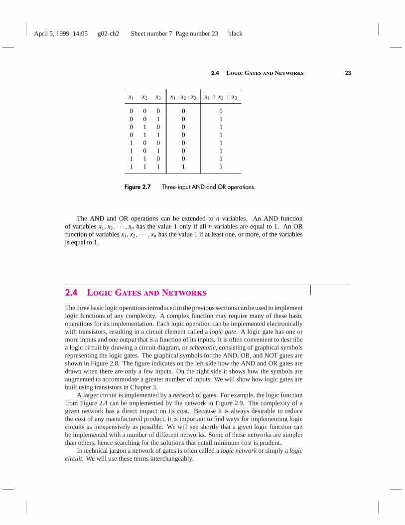
We have introduced the three most basic logic operations—AND, OR, and complement—byrelating them to simple circuits built with switches. This approach gives these operations acertain “physical meaning.” The same operations can also be defined in the form of a table,called atruth table, as shown in Figure 2.6. The first two columns (to the left of the heavyvertical line) give all four possible combinations of logic values that the variablesx1 andx2
can have. The next column defines the AND operation for each combination of values ofx1
andx2, and the last column defines the OR operation. Because we will frequently need torefer to “combinations of logic values” applied to some variables, we will adopt a shorterterm,valuation, to denote such a combination of logic values.
The truth table is a useful aid for depicting information involving logic functions. Wewill use it in this book to define specific functions and to show the validity of certain func-tional relations. Small truth tables are easy to deal with. However, they grow exponentiallyin size with the number of variables. A truth table for three input variables has eight rowsbecause there are eight possible valuations of these variables. Such a table is given in Figure2.7, which defines three-input AND and OR functions. For four-input variables the truthtable has 16 rows, and so on.
x1 x2 x1 · x2 x1+ x2
0 0 0 00 1 0 11 0 0 11 1 1 1
AND OR
Figure 2.6 A truth table for the AND and OR operations.
April 5, 1999 14:05 g02-ch2 Sheet number 7 Page number 23 black
2.4 Logic Gates and Networks 23
x1 x2 x3 x1 · x2 · x3 x1+ x2 + x3
0 0 0 0 00 0 1 0 10 1 0 0 10 1 1 0 11 0 0 0 11 0 1 0 11 1 0 0 11 1 1 1 1
Figure 2.7 Three-input AND and OR operations.
The AND and OR operations can be extended ton variables. An AND functionof variablesx1, x2, · · · , xn has the value 1 only if alln variables are equal to 1. An ORfunction of variablesx1, x2, · · · , xn has the value 1 if at least one, or more, of the variablesis equal to 1.
2.4 Logic Gates and Networks
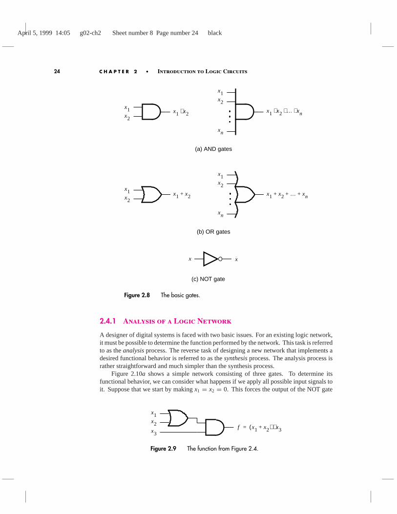
The three basic logic operations introduced in the previous sections can be used to implementlogic functions of any complexity. A complex function may require many of these basicoperations for its implementation. Each logic operation can be implemented electronicallywith transistors, resulting in a circuit element called alogic gate. A logic gate has one ormore inputs and one output that is a function of its inputs. It is often convenient to describea logic circuit by drawing a circuit diagram, orschematic, consisting of graphical symbolsrepresenting the logic gates. The graphical symbols for the AND, OR, and NOT gates areshown in Figure 2.8. The figure indicates on the left side how the AND and OR gates aredrawn when there are only a few inputs. On the right side it shows how the symbols areaugmented to accommodate a greater number of inputs. We will show how logic gates arebuilt using transistors in Chapter 3.
A larger circuit is implemented by anetworkof gates. For example, the logic functionfrom Figure 2.4 can be implemented by the network in Figure 2.9. The complexity of agiven network has a direct impact on its cost. Because it is always desirable to reducethe cost of any manufactured product, it is important to find ways for implementing logiccircuits as inexpensively as possible. We will see shortly that a given logic function canbe implemented with a number of different networks. Some of these networks are simplerthan others, hence searching for the solutions that entail minimum cost is prudent.
In technical jargon a network of gates is often called alogic networkor simply alogiccircuit. We will use these terms interchangeably.
April 5, 1999 14:05 g02-ch2 Sheet number 8 Page number 24 black
24 C H A P T E R 2 • Introduction to Logic Circuits
x1x2
xn
x1 x2 … xn+ + +x1x2
x1 x2+
x1x2
xn
x1x2
x1 x2⋅ x1 x2 … xn⋅ ⋅ ⋅
(a) AND gates
(b) OR gates
x x
(c) NOT gate
Figure 2.8 The basic gates.
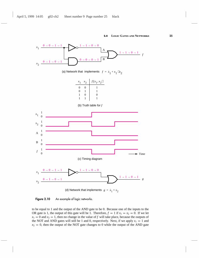
2.4.1 Analysis of a Logic Network
A designer of digital systems is faced with two basic issues. For an existing logic network,it must be possible to determine the function performed by the network. This task is referredto as theanalysisprocess. The reverse task of designing a new network that implements adesired functional behavior is referred to as thesynthesisprocess. The analysis process israther straightforward and much simpler than the synthesis process.
Figure 2.10a shows a simple network consisting of three gates. To determine itsfunctional behavior, we can consider what happens if we apply all possible input signals toit. Suppose that we start by makingx1 = x2 = 0. This forces the output of the NOT gate
x1x2x3
f x1 x2+( ) x3⋅=
Figure 2.9 The function from Figure 2.4.
April 5, 1999 14:05 g02-ch2 Sheet number 9 Page number 25 black
2.4 Logic Gates and Networks 25
x1
x2
1 1 0 0→ → →
f
0 0 0 1→ → →
1 1 0 1→ → →
0 0 1 1→ → →
0 1 0 1→ → →
(a) Network that implements f x1 x1 x2⋅+=
x1 x2 f x1 x2,( )
0101
0011
1101
(b) Truth table for f
A
B
10
10
10
10
10
x1
x2
A
B
fTime
(c) Timing diagram
1 1 0 0→ → →0 0 1 1→ → →
1 1 0 1→ → →0 1 0 1→ → → g
x1
x2
(d) Network that implements g x1 x2+=
Figure 2.10 An example of logic networks.
to be equal to 1 and the output of the AND gate to be 0. Because one of the inputs to theOR gate is 1, the output of this gate will be 1. Therefore,f = 1 if x1 = x2 = 0. If we letx1 = 0 andx2 = 1, then no change in the value off will take place, because the outputs ofthe NOT and AND gates will still be 1 and 0, respectively. Next, if we applyx1 = 1 andx2 = 0, then the output of the NOT gate changes to 0 while the output of the AND gate
April 5, 1999 14:05 g02-ch2 Sheet number 10 Page number 26 black
26 C H A P T E R 2 • Introduction to Logic Circuits
remains at 0. Both inputs to the OR gate are then equal to 0; hence the value off will be 0.Finally, letx1 = x2 = 1. Then the output of the AND gate goes to 1, which in turn causesf to be equal to 1. Our verbal explanation can be summarized in the form of the truth tableshown in Figure 2.10b.
Timing DiagramWe have determined the behavior of the network in Figure 2.10aby considering the four
possible valuations of the inputsx1 andx2. Suppose that the signals that correspond to thesevaluations are applied to the network in the order of our discussion; that is,(x1, x2) = (0, 0)followed by(0, 1), (1, 0), and(1, 1). Then changes in the signals at various points in thenetwork would be as indicated in blue in the figure. The same information can be presentedin graphical form, known as atiming diagram, as shown in Figure 2.10c. The time runsfrom left to right, and each input valuation is held for some fixed period. The figure showsthe waveforms for the inputs and output of the network, as well as for the internal signalsat the points labeledA andB.
Timing diagrams are used for many purposes. They depict the behavior of a logiccircuit in a form that can be observed when the circuit is tested using instruments such aslogic analyzers and oscilloscopes. Also, they are often generated by CAD tools to showthe designer how a given circuit is expected to behave before it is actually implementedelectronically. We will introduce the CAD tools later in this chapter and will make use ofthem throughout the book.
Functionally Equivalent NetworksNow consider the network in Figure 2.10d. Going through the same analysis procedure,
we find that the outputg changes in exactly the same way asf does in part (a) of the figure.Therefore,g(x1, x2) = f (x1, x2), which indicates that the two networks are functionallyequivalent; the output behavior of both networks is represented by the truth table in Figure2.10b. Since both networks realize the same function, it makes sense to use the simplerone, which is less costly to implement.
In general, a logic function can be implemented with a variety of different networks,probably having different costs. This raises an important question: How does one find thebest implementation for a given function? Many techniques exist for synthesizing logicfunctions. We will discuss the main approaches in Chapter 4. For now, we should note thatsome manipulation is needed to transform the more complex network in Figure 2.10a intothe network in Figure 2.10d. Sincef (x1, x2) = x1 + x1 · x2 andg(x1, x2) = x1 + x2, theremust exist some rules that can be used to show the equivalence
x1+ x1 · x2 = x1+ x2
We have already established this equivalence through detailed analysis of the two circuits andconstruction of the truth table. But the same outcome can be achieved through algebraicmanipulation of logic expressions. In the next section we will discuss a mathematicalapproach for dealing with logic functions, which provides the basis for modern designtechniques.
April 5, 1999 14:05 g02-ch2 Sheet number 11 Page number 27 black
2.5 Boolean Algebra 27
2.5 Boolean Algebra
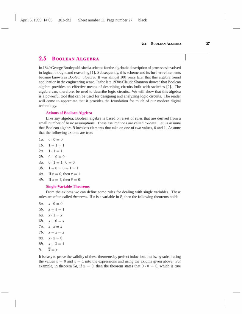
In 1849 George Boole published a scheme for the algebraic description of processes involvedin logical thought and reasoning [1]. Subsequently, this scheme and its further refinementsbecame known asBoolean algebra. It was almost 100 years later that this algebra foundapplication in the engineering sense. In the late 1930s Claude Shannon showed that Booleanalgebra provides an effective means of describing circuits built with switches [2]. Thealgebra can, therefore, be used to describe logic circuits. We will show that this algebrais a powerful tool that can be used for designing and analyzing logic circuits. The readerwill come to appreciate that it provides the foundation for much of our modern digitaltechnology.
Axioms of Boolean AlgebraLike any algebra, Boolean algebra is based on a set of rules that are derived from a
small number of basic assumptions. These assumptions are calledaxioms. Let us assumethat Boolean algebraB involves elements that take on one of two values, 0 and 1. Assumethat the following axioms are true:
1a. 0 · 0= 0
1b. 1+ 1= 1
2a. 1 · 1= 1
2b. 0+ 0= 0
3a. 0 · 1= 1 · 0= 0
3b. 1+ 0= 0+ 1= 1
4a. If x = 0, thenx = 1
4b. If x = 1, thenx = 0
Single-Variable TheoremsFrom the axioms we can define some rules for dealing with single variables. These
rules are often calledtheorems. If x is a variable inB, then the following theorems hold:
5a. x · 0= 0
5b. x+ 1= 1
6a. x · 1= x
6b. x+ 0= x
7a. x · x = x
7b. x+ x = x
8a. x · x = 0
8b. x+ x = 1
9. x = x
It is easy to prove the validity of these theorems by perfect induction, that is, by substitutingthe valuesx = 0 andx = 1 into the expressions and using the axioms given above. Forexample, in theorem 5a, if x = 0, then the theorem states that 0· 0 = 0, which is true
April 5, 1999 14:05 g02-ch2 Sheet number 12 Page number 28 black
28 C H A P T E R 2 • Introduction to Logic Circuits
according to axiom 1a. Similarly, if x = 1, then theorem 5a states that 1· 0 = 0, whichis also true according to axiom 3a. The reader should verify that theorems 5a to 9 can beproven in this way.
DualityNotice that we have listed the axioms and the single-variable theorems in pairs. This
is done to reflect the importantprinciple of duality. Given a logic expression, itsdual isobtained by replacing all+ operators with· operators, and vice versa, and by replacingall 0s with 1s, and vice versa. The dual of any true statement (axiom or theorem) inBoolean algebra is also a true statement. At this point in the discussion, the reader willnot appreciate why duality is a useful concept. However, this concept will become clearlater in the chapter, when we will show that duality implies that at least two different waysexist to express every logic function with Boolean algebra. Often, one expression leads toa simpler physical implementation than the other and is thus preferable.
Two- and Three-Variable PropertiesTo enable us to deal with a number of variables, it is useful to define some two- and
three-variable algebraic identities. For each identity, its dual version is also given. Theseidentities are often referred to asproperties. They are known by the names indicated below.If x, y, andz are the variables inB, then the following properties hold:
10a. x · y= y · x Commutative
10b. x+ y= y+ x
11a. x · ( y · z) = (x · y) · z Associative
11b. x+ ( y+ z) = (x+ y)+ z
12a. x · ( y+ z) = x · y+ x · z Distributive
12b. x+ y · z= (x+ y) · (x+ z)
13a. x+ x · y= x Absorption
13b. x · (x+ y) = x
14a. x · y+ x · y= x Combining
14b. (x+ y) · (x+ y) = x
15a. x · y= x+ y DeMorgan’s theorem
15b. x+ y= x · y16a. x+ x · y= x+ y
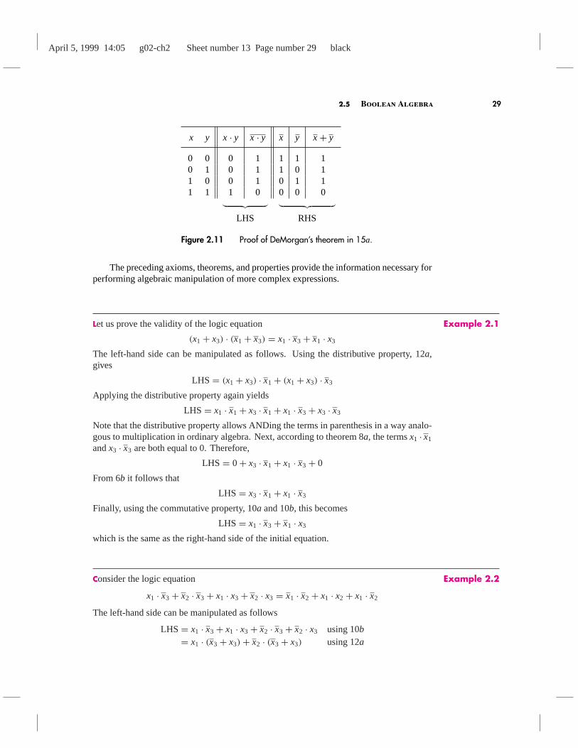
16b. x · (x+ y) = x · yAgain, we can prove the validity of these properties either by perfect induction or byperforming algebraic manipulation. Figure 2.11 illustrates how perfect induction can beused to prove DeMorgan’s theorem, using the format of a truth table. The evaluation ofleft-hand and right-hand sides of the identity in 15a gives the same result.
We have listed a number of axioms, theorems, and properties. Not all of these arenecessary to define Boolean algebra. For example, assuming that the+ and· operationsare defined, it is sufficient to include theorems 5 and 8 and properties 10 and 12. Theseare sometimes referred to as Huntington’s basic postulates [3]. The other identities can bederived from these postulates.
April 5, 1999 14:05 g02-ch2 Sheet number 13 Page number 29 black
2.5 Boolean Algebra 29
x y x · y x · y x y x+ y
0 0 0 1 1 1 10 1 0 1 1 0 11 0 0 1 0 1 11 1 1 0 0 0 0︸ ︷︷ ︸ ︸ ︷︷ ︸
LHS RHS
Figure 2.11 Proof of DeMorgan’s theorem in 15a.
The preceding axioms, theorems, and properties provide the information necessary forperforming algebraic manipulation of more complex expressions.
Example 2.1Let us prove the validity of the logic equation
(x1+ x3) · (x1+ x3) = x1 · x3+ x1 · x3
The left-hand side can be manipulated as follows. Using the distributive property, 12a,gives
LHS= (x1+ x3) · x1+ (x1+ x3) · x3
Applying the distributive property again yields
LHS= x1 · x1+ x3 · x1+ x1 · x3+ x3 · x3
Note that the distributive property allows ANDing the terms in parenthesis in a way analo-gous to multiplication in ordinary algebra. Next, according to theorem 8a, the termsx1 · x1
andx3 · x3 are both equal to 0. Therefore,
LHS= 0+ x3 · x1+ x1 · x3+ 0
From 6b it follows that
LHS= x3 · x1+ x1 · x3
Finally, using the commutative property, 10a and 10b, this becomes
LHS= x1 · x3+ x1 · x3
which is the same as the right-hand side of the initial equation.
Example 2.2Consider the logic equation
x1 · x3+ x2 · x3+ x1 · x3+ x2 · x3 = x1 · x2 + x1 · x2 + x1 · x2
The left-hand side can be manipulated as follows
LHS= x1 · x3+ x1 · x3+ x2 · x3+ x2 · x3 using 10b= x1 · (x3+ x3)+ x2 · (x3+ x3) using 12a
April 5, 1999 14:05 g02-ch2 Sheet number 14 Page number 30 black
30 C H A P T E R 2 • Introduction to Logic Circuits
= x1 · 1+ x2 · 1 using 8b= x1+ x2 using 6a
The right-hand side can be manipulated as
RHS= x1 · x2 + x1 · (x2 + x2) using 12a= x1 · x2 + x1 · 1 using 8b= x1 · x2 + x1 using 6a= x1+ x1 · x2 using 10b= x1+ x2 using 16a
Being able to manipulate both sides of the initial equation into identical expressions estab-lishes the validity of the equation. Note that the same logic function is represented by eitherthe left- or the right-hand side of the above equation; namely
f (x1, x2, x3) = x1 · x3+ x2 · x3+ x1 · x3+ x2 · x3
= x1 · x2 + x1 · x2 + x1 · x2
As a result of manipulation, we have found a much simpler expression
f (x1, x2, x3) = x1+ x2
which also represents the same function. This simpler expression would result in a lower-cost logic circuit that could be used to implement the function.
Examples 2.1 and 2.2 illustrate the purpose of the axioms, theorems, and propertiesas a mechanism for algebraic manipulation. Even these simple examples suggest that it isimpractical to deal with highly complex expressions in this way. However, these theoremsand properties provide the basis for automating the synthesis of logic functions in CADtools. To understand what can be achieved using these tools, the designer needs to be awareof the fundamental concepts.
2.5.1 The Venn Diagram
We have suggested that perfect induction can be used to verify the theorems and properties.This procedure is quite tedious and not very informative from the conceptual point of view.A simple visual aid that can be used for this purpose also exists. It is called the Venndiagram, and the reader is likely to find that it provides for a more intuitive understandingof how two expressions may be equivalent.
The Venn diagram has traditionally been used in mathematics to provide a graphicalillustration of various operations and relations in the algebra of sets. A sets is a collectionof elements that are said to be the members ofs. In the Venn diagram the elements ofa set are represented by the area enclosed by a contour such as a square, a circle, or anellipse. For example, in a universeN of integers from 1 to 10, the set of even numbers isE = {2, 4, 6, 8, 10}. A contour representingE encloses the even numbers. The odd numbersform the complement ofE; hence the area outside the contour representsE = {1, 3, 5, 7, 9}.
April 5, 1999 14:05 g02-ch2 Sheet number 15 Page number 31 black
2.5 Boolean Algebra 31
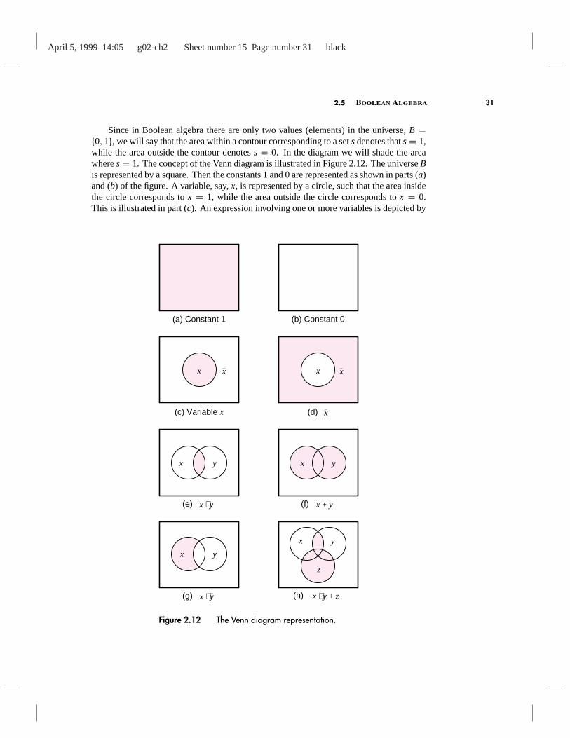
Since in Boolean algebra there are only two values (elements) in the universe,B ={0, 1}, we will say that the area within a contour corresponding to a setsdenotes thats= 1,while the area outside the contour denotess = 0. In the diagram we will shade the areawheres= 1. The concept of the Venn diagram is illustrated in Figure 2.12. The universeBis represented by a square. Then the constants 1 and 0 are represented as shown in parts (a)and (b) of the figure. A variable, say,x, is represented by a circle, such that the area insidethe circle corresponds tox = 1, while the area outside the circle corresponds tox = 0.This is illustrated in part (c). An expression involving one or more variables is depicted by
x y
z
x y
x y x y
x x xx
(a) Constant 1 (b) Constant 0
(c) Variable x (d)
(e) (f)
(g) (h)
x
x y⋅ x y+
x y z+⋅x y⋅
Figure 2.12 The Venn diagram representation.
April 5, 1999 14:05 g02-ch2 Sheet number 16 Page number 32 black
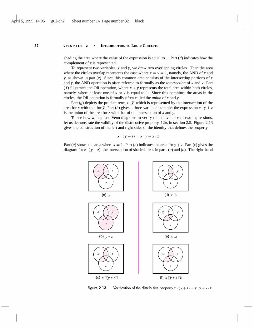
32 C H A P T E R 2 • Introduction to Logic Circuits
shading the area where the value of the expression is equal to 1. Part (d) indicates how thecomplement ofx is represented.
To represent two variables,x andy, we draw two overlapping circles. Then the areawhere the circles overlap represents the case wherex = y = 1, namely, the AND ofx andy, as shown in part (e). Since this common area consists of the intersecting portions ofxandy, the AND operation is often referred to formally as theintersectionof x andy. Part( f ) illustrates the OR operation, wherex+ y represents the total area within both circles,namely, where at least one ofx or y is equal to 1. Since this combines the areas in thecircles, the OR operation is formally often called theunionof x andy.
Part (g) depicts the product termx · y, which is represented by the intersection of thearea forx with that fory. Part (h) gives a three-variable example; the expressionx · y+ zis the union of the area forz with that of the intersection ofx andy.
To see how we can use Venn diagrams to verify the equivalence of two expressions,let us demonstrate the validity of the distributive property, 12a, in section 2.5. Figure 2.13gives the construction of the left and right sides of the identity that defines the property
x · ( y+ z) = x · y+ x · zPart (a) shows the area wherex = 1. Part (b) indicates the area fory+ z. Part (c) gives thediagram forx · ( y+ z), the intersection of shaded areas in parts (a) and (b). The right-hand
x y
z
x y
z
x y
z
x y
z
x y
z
x y
z
x x y⋅
x y⋅ x+ z⋅x y z+( )⋅
(a) (d)
(c) (f)
x z⋅y z+(b) (e)
Figure 2.13 Verification of the distributive property x · ( y+ z) = x · y+ x · z.
April 5, 1999 14:05 g02-ch2 Sheet number 17 Page number 33 black
2.5 Boolean Algebra 33
side is constructed in parts (d ), (e), and (f ). Parts (d ) and (e) describe the termsx · y andx · z, respectively. The union of the shaded areas in these two diagrams then correspondsto the expressionx · y+ x · z, as seen in part (f ). Since the shaded areas in parts (c) and (f )are identical, it follows that the distributive property is valid.
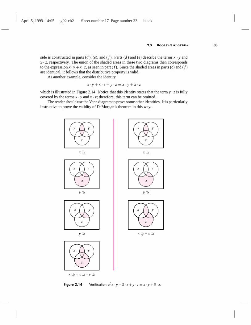
As another example, consider the identity
x · y+ x · z+ y · z= x · y+ x · zwhich is illustrated in Figure 2.14. Notice that this identity states that the termy · z is fullycovered by the termsx · y andx · z; therefore, this term can be omitted.
The reader should use the Venn diagram to prove some other identities. It is particularlyinstructive to prove the validity of DeMorgan’s theorem in this way.
x y
z
yx
z
x y
z
x y⋅
y z⋅ x y⋅ x+ z⋅
x z⋅
x y
z
x y⋅
x y
z
x z⋅
x y⋅ x+ z y z⋅+⋅
x y
z
x y
z
Figure 2.14 Verification of x · y+ x · z+ y · z= x · y+ x · z.
April 5, 1999 14:05 g02-ch2 Sheet number 18 Page number 34 black
34 C H A P T E R 2 • Introduction to Logic Circuits
2.5.2 Notation and Terminology
Boolean algebra is based on the AND and OR operations. We have adopted the symbols· and+ to denote these operations. These are also the standard symbols for the familiararithmetic multiplication and addition operations. Considerable similarity exists betweenthe Boolean operations and the arithmetic operations, which is the main reason why thesame symbols are used. In fact, when single digits are involved there is only one significantdifference; the result of 1+ 1 is equal to 2 in ordinary arithmetic, whereas it is equal to 1in Boolean algebra as defined by theorem 7b in section 2.5.
When dealing with digital circuits, most of the time the+ symbol obviously representsthe OR operation. However, when the task involves the design of logic circuits that performarithmetic operations, some confusion may develop about the use of the+ symbol. Toavoid such confusion, an alternative set of symbols exists for the AND and OR operations.It is quite common to use the∧ symbol to denote the AND operation, and the∨ symbol forthe OR operation. Thus, instead ofx1 · x2, we can writex1 ∧ x2, and instead ofx1+ x2, wecan writex1 ∨ x2.
Because of the similarity with the arithmetic addition and multiplication operations,the OR and AND operations are often called thelogical sumandproductoperations. Thusx1+ x2 is the logical sum ofx1 andx2, andx1 · x2 is the logical product ofx1 andx2. Insteadof saying “logical product” and “logical sum,” it is customary to say simply “product” and“sum.” Thus we say that the expression
x1 · x2 · x3+ x1 · x4 + x2 · x3 · x4
is a sum of three product terms, whereas the expression
(x1+ x3) · (x1+ x3) · (x2 + x3+ x4)
is a product of three sum terms.
2.5.3 Precedence of Operations
Using the three basic operations—AND, OR, and NOT—it is possible to construct an infinitenumber of logic expressions. Parentheses can be used to indicate the order in which theoperations should be performed. However, to avoid an excessive use of parentheses, anotherconvention defines the precedence of the basic operations. It states that in the absence ofparentheses, operations in a logic expression must be performed in the order: NOT, AND,and then OR. Thus in the expression
x1 · x2 + x1 · x2
it is first necessary to generate the complements ofx1 andx2. Then the product termsx1 · x2
andx1 · x2 are formed, followed by the sum of the two product terms. Observe that in theabsence of this convention, we would have to use parentheses to achieve the same effect asfollows:
(x1 · x2)+ ((x1) · (x2))
April 5, 1999 14:05 g02-ch2 Sheet number 19 Page number 35 black
2.6 Synthesis Using AND, OR, and NOT Gates 35
Finally, to simplify the appearance of logic expressions, it is customary to omit the·operator when there is no ambiguity. Therefore, the preceding expression can be written as
x1x2 + x1x2
We will use this style throughout the book.
2.6 Synthesis Using AND, OR, and NOT Gates
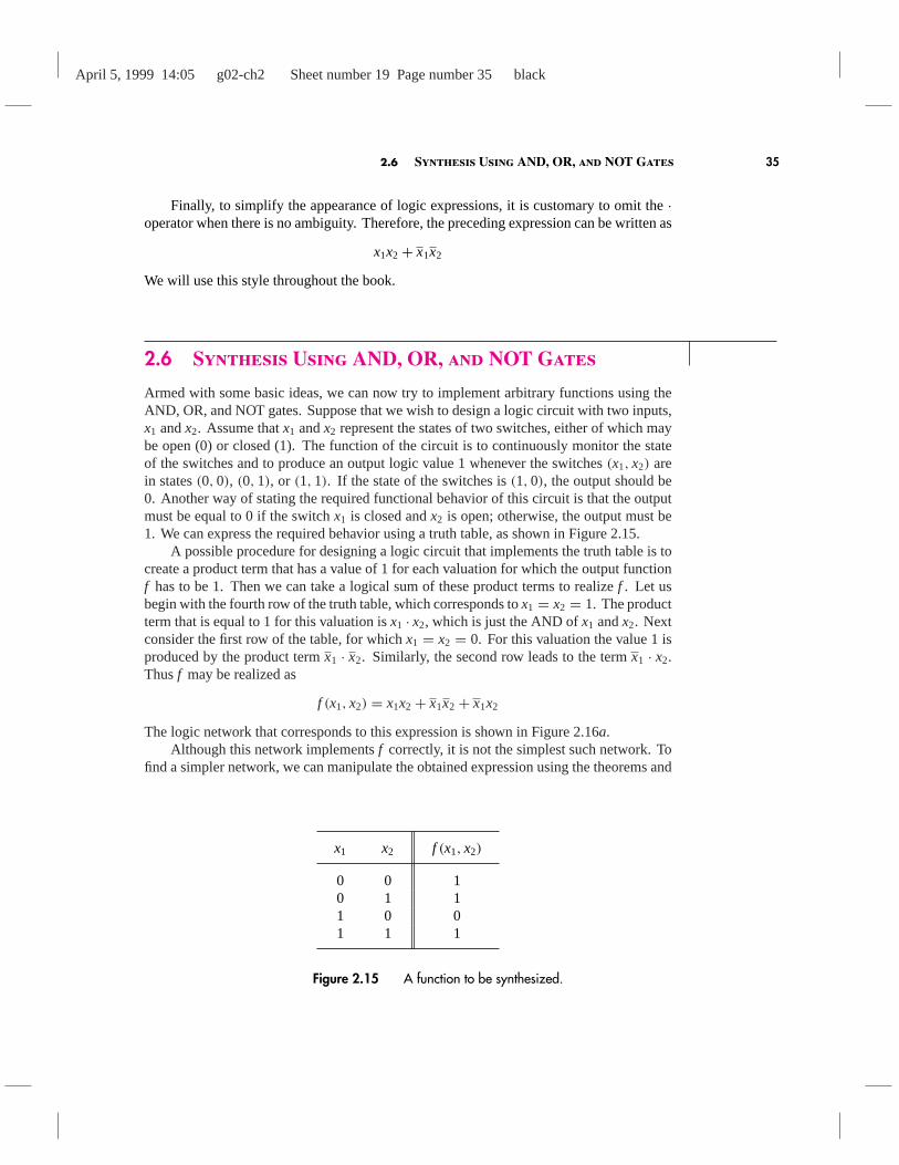
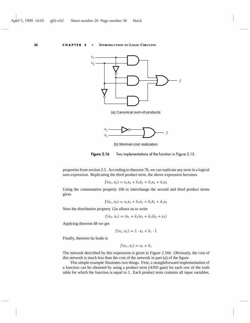
Armed with some basic ideas, we can now try to implement arbitrary functions using theAND, OR, and NOT gates. Suppose that we wish to design a logic circuit with two inputs,x1 andx2. Assume thatx1 andx2 represent the states of two switches, either of which maybe open (0) or closed (1). The function of the circuit is to continuously monitor the stateof the switches and to produce an output logic value 1 whenever the switches(x1, x2) arein states(0, 0), (0, 1), or (1, 1). If the state of the switches is(1, 0), the output should be0. Another way of stating the required functional behavior of this circuit is that the outputmust be equal to 0 if the switchx1 is closed andx2 is open; otherwise, the output must be1. We can express the required behavior using a truth table, as shown in Figure 2.15.
A possible procedure for designing a logic circuit that implements the truth table is tocreate a product term that has a value of 1 for each valuation for which the output functionf has to be 1. Then we can take a logical sum of these product terms to realizef . Let usbegin with the fourth row of the truth table, which corresponds tox1 = x2 = 1. The productterm that is equal to 1 for this valuation isx1 · x2, which is just the AND ofx1 andx2. Nextconsider the first row of the table, for whichx1 = x2 = 0. For this valuation the value 1 isproduced by the product termx1 · x2. Similarly, the second row leads to the termx1 · x2.Thusf may be realized as
f (x1, x2) = x1x2 + x1x2 + x1x2
The logic network that corresponds to this expression is shown in Figure 2.16a.Although this network implementsf correctly, it is not the simplest such network. To
find a simpler network, we can manipulate the obtained expression using the theorems and
x1 x2 f (x1, x2)
0 0 10 1 11 0 01 1 1
Figure 2.15 A function to be synthesized.
April 5, 1999 14:05 g02-ch2 Sheet number 20 Page number 36 black
36 C H A P T E R 2 • Introduction to Logic Circuits
f
(a) Canonical sum-of-products
f
(b) Minimal-cost realization
x2
x1
x1
x2
Figure 2.16 Two implementations of the function in Figure 2.15.
properties from section 2.5. According to theorem 7b, we can replicate any term in a logicalsum expression. Replicating the third product term, the above expression becomes
f (x1, x2) = x1x2 + x1x2 + x1x2 + x1x2
Using the commutative property 10b to interchange the second and third product termsgives
f (x1, x2) = x1x2 + x1x2 + x1x2 + x1x2
Now the distributive property 12a allows us to write
f (x1, x2) = (x1+ x1)x2 + x1(x2 + x2)
Applying theorem 8b we get
f (x1, x2) = 1 · x2 + x1 · 1Finally, theorem 6a leads to
f (x1, x2) = x2 + x1
The network described by this expression is given in Figure 2.16b. Obviously, the cost ofthis network is much less than the cost of the network in part (a) of the figure.
This simple example illustrates two things. First, a straightforward implementation ofa function can be obtained by using a product term (AND gate) for each row of the truthtable for which the function is equal to 1. Each product term contains all input variables,
April 5, 1999 14:05 g02-ch2 Sheet number 21 Page number 37 black
2.6 Synthesis Using AND, OR, and NOT Gates 37
and it is formed such that if the input variablexi is equal to 1 in the given row, thenxi isentered in the term; ifxi = 0, thenxi is entered. The sum of these product terms realizesthe desired function. Second, there are many different networks that can realize a givenfunction. Some of these networks may be simpler than others. Algebraic manipulation canbe used to derive simplified logic expressions and thus lower-cost networks.
The process whereby we begin with a description of the desired functional behaviorand then generate a circuit that realizes this behavior is calledsynthesis. Thus we cansay that we “synthesized” the networks in Figure 2.16 from the truth table in Figure 2.15.Generation of AND-OR expressions from a truth table is just one of many types of synthesistechniques that we will encounter in this book.
2.6.1 Sum-of-Products and Product-of-Sums Forms
Having introduced the synthesis process by means of a very simple example, we will nowpresent it in more formal terms using the terminology that is encountered in the technicalliterature. We will also show how the principle of duality, which was introduced in section2.5, applies broadly in the synthesis process.
If a functionf is specified in the form of a truth table, then an expression that realizesf can be obtained by considering either the rows in the table for whichf = 1, as we havealready done, or by considering the rows for whichf = 0, as we will explain shortly.
MintermsFor a function ofn variables, a product term in which each of then variables appears
once is called aminterm. The variables may appear in a minterm either in uncomplementedor complemented form. For a given row of the truth table, the minterm is formed byincludingxi if xi = 1 and by includingxi if xi = 0.
To illustrate this concept, consider the truth table in Figure 2.17. We have num-bered the rows of the table from 0 to 7, so that we can refer to them easily. (Thereader who is already familiar with the binary number representation will realize that therow numbers chosen are just the numbers represented by the bit patterns of variablesx1,x2, andx3; we will discuss number representation in Chapter 5.) The figure shows allminterms for the three-variable table. For example, in the first row the variables havethe valuesx1 = x2 = x3 = 0, which leads to the mintermx1x2x3. In the second rowx1 = x2 = 0 andx3 = 1, which gives the mintermx1x2x3, and so on. To be able torefer to the individual minterms easily, it is convenient to identify each minterm by anindex that corresponds to the row numbers shown in the figure. We will use the nota-tion mi to denote the minterm for row numberi. Thusm0 = x1x2x3, m1 = x1x2x3, andso on.
Sum-of-Products FormA functionf can be represented by an expression that is a sum of minterms, where each
minterm is ANDed with the value off for the corresponding valuation of input variables.For example, the two-variable minterms arem0 = x1x2, m1 = x1x2, m2 = x1x2, andm3 = x1x2. The function in Figure 2.15 can be represented as
April 5, 1999 14:05 g02-ch2 Sheet number 22 Page number 38 black
38 C H A P T E R 2 • Introduction to Logic Circuits
Rownumber x1 x2 x3 Minterm Maxterm
0 0 0 0 m0 = x1x2x3 M0 = x1+ x2 + x3
1 0 0 1 m1 = x1x2x3 M1 = x1+ x2 + x3
2 0 1 0 m2 = x1x2x3 M2 = x1+ x2 + x3
3 0 1 1 m3 = x1x2x3 M3 = x1+ x2 + x3
4 1 0 0 m4 = x1x2x3 M4 = x1+ x2 + x3
5 1 0 1 m5 = x1x2x3 M5 = x1+ x2 + x3
6 1 1 0 m6 = x1x2x3 M6 = x1+ x2 + x3
7 1 1 1 m7 = x1x2x3 M7 = x1+ x2 + x3
Figure 2.17 Three-variable minterms and maxterms.
f = m0 · 1+m1 · 1+m2 · 0+m3 · 1= m0 +m1+m3
= x1x2 + x1x2 + x1x2
which is the form that we derived in the previous section using an intuitive approach. Onlythe minterms that correspond to the rows for whichf = 1 appear in the resulting expression.
Any function f can be represented by a sum of minterms that correspond to the rowsin the truth table for whichf = 1. The resulting implementation is functionally correct andunique, but it is not necessarily the lowest-cost implementation off . A logic expressionconsisting of product (AND) terms that are summed (ORed) is said to be of thesum-of-productsform. If each product term is a minterm, then the expression is called acanonicalsum-of-productsfor the functionf . As we have seen in the example of Figure 2.16, the firststep in the synthesis process is to derive a canonical sum-of-products expression for thegiven function. Then we can manipulate this expression, using the theorems and propertiesof section 2.5, with the goal of finding a functionally equivalent sum-of-products expressionthat has a lower cost.
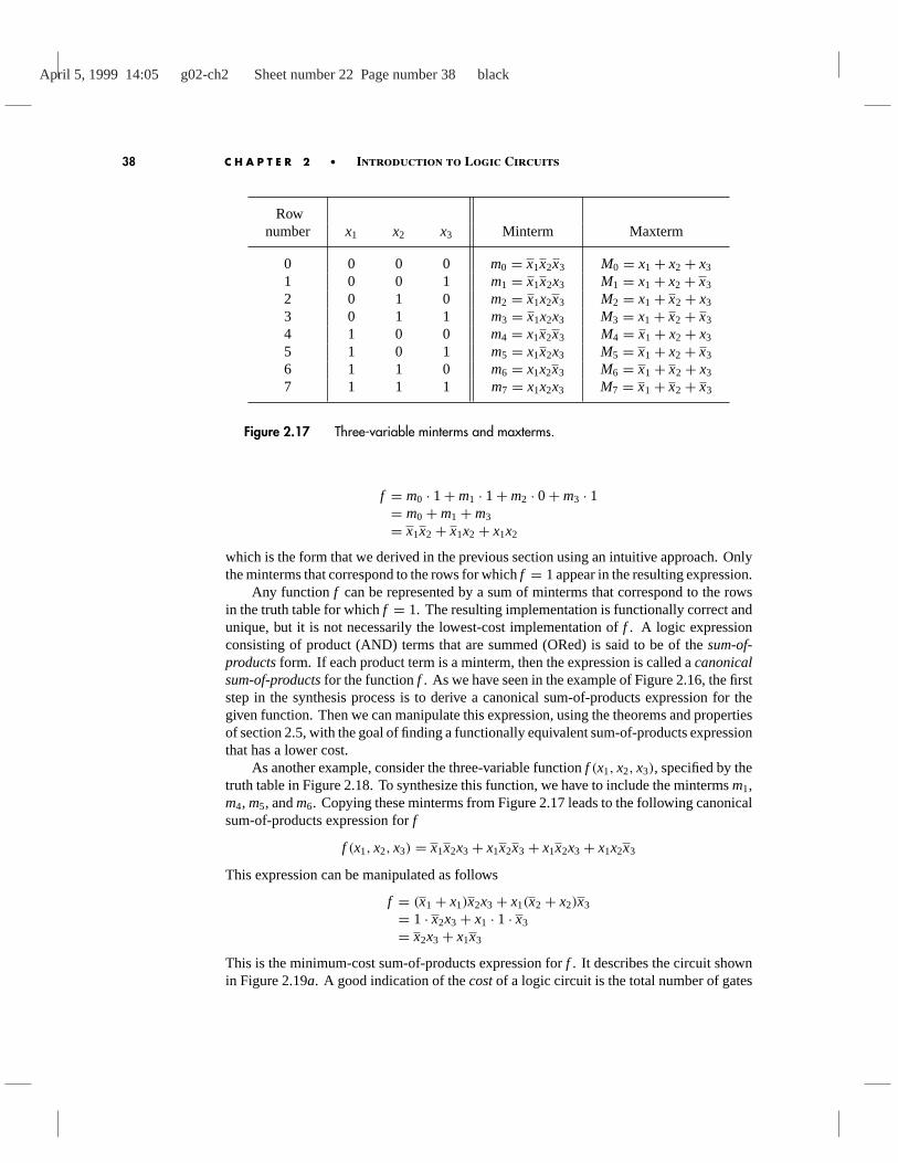
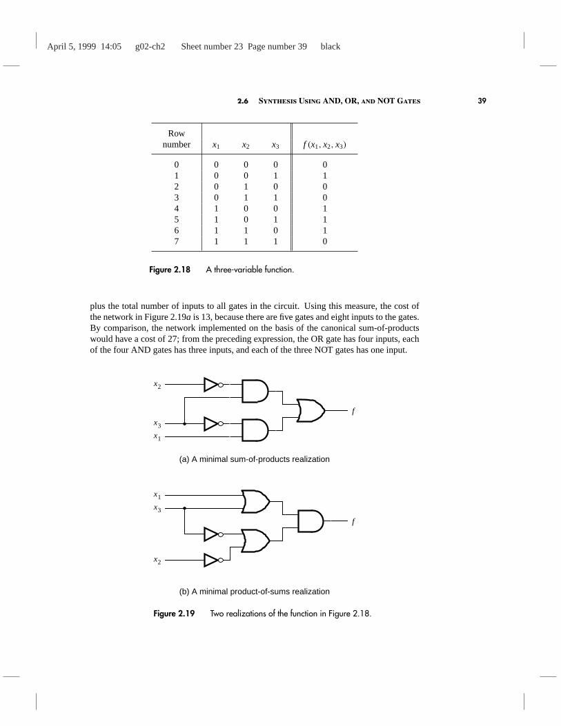
As another example, consider the three-variable functionf (x1, x2, x3), specified by thetruth table in Figure 2.18. To synthesize this function, we have to include the mintermsm1,m4, m5, andm6. Copying these minterms from Figure 2.17 leads to the following canonicalsum-of-products expression forf
f (x1, x2, x3) = x1x2x3+ x1x2x3+ x1x2x3+ x1x2x3
This expression can be manipulated as follows
f = (x1+ x1)x2x3+ x1(x2 + x2)x3
= 1 · x2x3+ x1 · 1 · x3
= x2x3+ x1x3
This is the minimum-cost sum-of-products expression forf . It describes the circuit shownin Figure 2.19a. A good indication of thecostof a logic circuit is the total number of gates
April 5, 1999 14:05 g02-ch2 Sheet number 23 Page number 39 black
2.6 Synthesis Using AND, OR, and NOT Gates 39
Rownumber x1 x2 x3 f (x1, x2, x3)
0 0 0 0 01 0 0 1 12 0 1 0 03 0 1 1 04 1 0 0 15 1 0 1 16 1 1 0 17 1 1 1 0
Figure 2.18 A three-variable function.
plus the total number of inputs to all gates in the circuit. Using this measure, the cost ofthe network in Figure 2.19a is 13, because there are five gates and eight inputs to the gates.By comparison, the network implemented on the basis of the canonical sum-of-productswould have a cost of 27; from the preceding expression, the OR gate has four inputs, eachof the four AND gates has three inputs, and each of the three NOT gates has one input.
f
(a) A minimal sum-of-products realization
f
(b) A minimal product-of-sums realization
x1
x2
x3
x2
x1
x3
Figure 2.19 Two realizations of the function in Figure 2.18.
April 5, 1999 14:05 g02-ch2 Sheet number 24 Page number 40 black
40 C H A P T E R 2 • Introduction to Logic Circuits
Minterms, with their row-number subscripts, can also be used to specify a given functionin a more concise form. For example, the function in Figure 2.18 can be specified as
f (x1, x2, x3) =∑
(m1,m4,m5,m6)
or even more simply as
f (x1, x2, x3) =∑
m(1, 4, 5, 6)
The∑
sign denotes the logical sum operation. This shorthand notation is often used inpractice.
MaxtermsThe principle of duality suggests that if it is possible to synthesize a functionf by
considering the rows in the truth table for whichf = 1, then it should also be possible tosynthesizef by considering the rows for whichf = 0. This alternative approach uses thecomplements of minterms, which are calledmaxterms. All possible maxterms for three-variable functions are listed in Figure 2.17. We will refer to a maxtermMj by the same rownumber as its corresponding mintermmj as shown in the figure.
Product-of-Sums FormIf a given functionf is specified by a truth table, then its complementf can be rep-
resented by a sum of minterms for whichf = 1, which are the rows wheref = 0. Forexample, for the function in Figure 2.15
f (x1, x2) = m2
= x1x2
If we complement this expression using DeMorgan’s theorem, the result is
f = f = x1x2
= x1+ x2
Note that we obtained this expression previously by algebraic manipulation of the canonicalsum-of-products form for the functionf . The key point here is that
f = m2 = M2
whereM2 is the maxterm for row 2 in the truth table.As another example, consider again the function in Figure 2.18. The complement of
this function can be represented as
f (x1, x2, x3)=m0 +m2 +m3+m7
= x1x2x3+ x1x2x3+ x1x2x3+ x1x2x3
Thenf can be expressed as
f =m0 +m2 +m3+m7
=m0 ·m2 ·m3 ·m7
April 5, 1999 14:05 g02-ch2 Sheet number 25 Page number 41 black
2.7 Design Examples 41
=M0 ·M2 ·M3 ·M7
= (x1+ x2 + x3)(x1+ x2 + x3)(x1+ x2 + x3)(x1+ x2 + x3)
This expression representsf as a product of maxterms.A logic expression consisting of sum (OR) terms that are the factors of a logical product
(AND) is said to be of theproduct-of-sumsform. If each sum term is a maxterm, then theexpression is called acanonical product-of-sumsfor the given function. Any functionf canbe synthesized by finding its canonical product-of-sums. This involves taking the maxtermfor each row in the truth table for whichf = 0 and forming a product of these maxterms.
Returning to the preceding example, we can attempt to reduce the complexity of thederived expression that comprises a product of maxterms. Using the commutative property10b and the associative property 11b from section 2.5, this expression can be written as
f = ((x1+ x3)+ x2)((x1+ x3)+ x2)(x1+ (x2 + x3))(x1+ (x2 + x3))
Then, using the combining property 14b, the expression reduces to
f = (x1+ x3)(x2 + x3)
The corresponding network is given in Figure 2.19b. The cost of this network is 13. Whilethis cost happens to be the same as the cost of the sum-of-products version in Figure 2.19a,the reader should not assume that the cost of a network derived in the sum-of-products formwill in general be equal to the cost of a corresponding circuit derived in the product-of-sumsform.
Using the shorthand notation, an alternative way of specifying our sample function is
f (x1, x2, x3) = 5(M0,M2,M3,M7)
or more simply
f (x1, x2, x3) = 5M(0, 2, 3, 7)
The5 sign denotes the logical product operation.The preceding discussion has shown how logic functions can be realized in the form
of logic circuits, consisting of networks of gates that implement basic functions. A givenfunction may be realized with circuits of a different structure, which usually implies adifference in cost. An important objective for a designer is to minimize the cost of thedesigned circuit. We will discuss the most important techniques for finding minimum-costimplementations in Chapter 4.
2.7 Design Examples
Logic circuits provide a solution to a problem. They implement functions that are needed tocarry out specific tasks. Within the framework of a computer, logic circuits provide completecapability for execution of programs and processing of data. Such circuits are complex anddifficult to design. But regardless of the complexity of a given circuit, a designer of logiccircuits is always confronted with the same basic issues. First, it is necessary to specify thedesired behavior of the circuit. Second, the circuit has to be synthesized and implemented.
April 5, 1999 14:05 g02-ch2 Sheet number 26 Page number 42 black
42 C H A P T E R 2 • Introduction to Logic Circuits
Finally, the implemented circuit has to be tested to verify that it meets the specifications.The desired behavior is often initially described in words, which then must be turned intoa formal specification. In this section we give two simple examples of design.
2.7.1 Three-Way Light Control
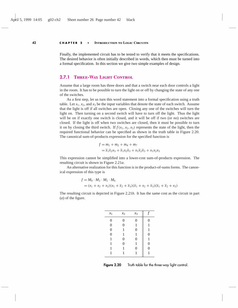
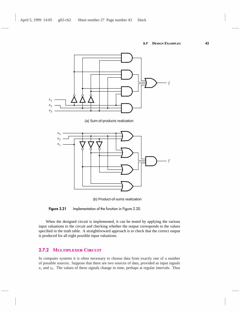
Assume that a large room has three doors and that a switch near each door controls a lightin the room. It has to be possible to turn the light on or off by changing the state of any oneof the switches.
As a first step, let us turn this word statement into a formal specification using a truthtable. Letx1, x2, andx3 be the input variables that denote the state of each switch. Assumethat the light is off if all switches are open. Closing any one of the switches will turn thelight on. Then turning on a second switch will have to turn off the light. Thus the lightwill be on if exactly one switch is closed, and it will be off if two (or no) switches areclosed. If the light is off when two switches are closed, then it must be possible to turnit on by closing the third switch. Iff (x1, x2, x3) represents the state of the light, then therequired functional behavior can be specified as shown in the truth table in Figure 2.20.The canonical sum-of-products expression for the specified function is
f =m1+m2 +m4 +m7
= x1x2x3+ x1x2x3+ x1x2x3+ x1x2x3
This expression cannot be simplified into a lower-cost sum-of-products expression. Theresulting circuit is shown in Figure 2.21a.
An alternative realization for this function is in the product-of-sums forms. The canon-ical expression of this type is
f =M0 ·M3 ·M5 ·M6
= (x1+ x2 + x3)(x1+ x2 + x3)(x1+ x2 + x3)(x1+ x2 + x3)
The resulting circuit is depicted in Figure 2.21b. It has the same cost as the circuit in part(a) of the figure.
x1 x2 x3 f
0 0 0 00 0 1 10 1 0 10 1 1 01 0 0 11 0 1 01 1 0 01 1 1 1
Figure 2.20 Truth table for the three-way light control.
April 5, 1999 14:05 g02-ch2 Sheet number 27 Page number 43 black
2.7 Design Examples 43
f
(a) Sum-of-products realization
(b) Product-of-sums realization
x1
x2
x3
f
x1
x2
x3
Figure 2.21 Implementation of the function in Figure 2.20.
When the designed circuit is implemented, it can be tested by applying the variousinput valuations to the circuit and checking whether the output corresponds to the valuesspecified in the truth table. A straightforward approach is to check that the correct outputis produced for all eight possible input valuations.
2.7.2 Multiplexer Circuit
In computer systems it is often necessary to choose data from exactly one of a numberof possible sources. Suppose that there are two sources of data, provided as input signalsx1 andx2. The values of these signals change in time, perhaps at regular intervals. Thus
April 5, 1999 14:05 g02-ch2 Sheet number 28 Page number 44 black
44 C H A P T E R 2 • Introduction to Logic Circuits
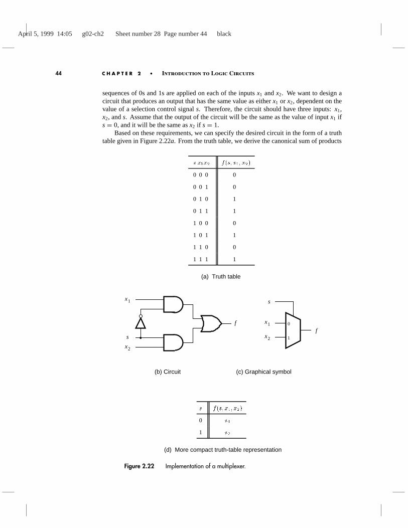
sequences of 0s and 1s are applied on each of the inputsx1 andx2. We want to design acircuit that produces an output that has the same value as eitherx1 or x2, dependent on thevalue of a selection control signals. Therefore, the circuit should have three inputs:x1,x2, ands. Assume that the output of the circuit will be the same as the value of inputx1 ifs= 0, and it will be the same asx2 if s= 1.
Based on these requirements, we can specify the desired circuit in the form of a truthtable given in Figure 2.22a. From the truth table, we derive the canonical sum of products
0 0 0 0
0 0 1 0
0 1 0 1
0 1 1 1
1 0 0 0
1 0 1 1
1 1 0 0
1 1 1 1
(a) Truth table
f
x1
x2
sf
s
x1
x2
0
1
(c) Graphical symbol(b) Circuit
0
1
(d) More compact truth-table representation
Figure 2.22 Implementation of a multiplexer.
April 5, 1999 14:05 g02-ch2 Sheet number 29 Page number 45 black
2.8 Introduction to CAD Tools 45
f (s, x1, x2) = sx1x2 + sx1x2 + sx1x2 + sx1x2
Using the distributive property, this expression can be written as
f = sx1(x2 + x2)+ s(x1+ x1)x2
Applying theorem 8b yields
f = sx1 · 1+ s · 1 · x2
Finally, theorem 6a gives
f = sx1+ sx2
A circuit that implements this function is shown in Figure 2.22b. Circuits of this type areused so extensively that they are given a special name. A circuit that generates an outputthat exactly reflects the state of one of a number of data inputs, based on the value of oneor more selection control inputs, is called amultiplexer. We say that a multiplexer circuit“multiplexes” input signals onto a single output.
In this example we derived a multiplexer with two data inputs, which is referred toas a “2-to-1 multiplexer.” A commonly used graphical symbol for the 2-to-1 multiplexeris shown in Figure 2.22c. The same idea can be extended to larger circuits. A 4-to-1multiplexer has four data inputs and one output. In this case two selection control inputsare needed to choose one of the four data inputs that is transmitted as the output signal. An8-to-1 multiplexer needs eight data inputs and three selection control inputs, and so on.
Note that the statement “f = x1 if s = 0, andf = x2 if s = 1” can be presented in amore compact form of a truth table, as indicated in Figure 2.22d. In later chapters we willhave occasion to use such representation.
We showed how a multiplexer can be built using AND, OR, and NOT gates. In Chap-ter 3 we will show other possibilities for constructing multiplexers. In Chapter 6 we willdiscuss the use of multiplexers in considerable detail.
Designers of logic circuits rely heavily on CAD tools. We want to encourage the readerto become familiar with the CAD tool support provided with this book as soon as possible.We have reached a point where an introduction to these tools is useful. The next sectionpresents some basic concepts that are needed to use these tools. We will also introduce, insection 2.9, a special language for describing logic circuits, called VHDL. This languageis used to describe the circuits as an input to the CAD tools, which then proceed to derivea suitable implementation.
2.8 Introduction to CAD Tools
The preceding sections introduced a basic approach for synthesis of logic circuits. Adesigner could use this approach manually for small circuits. However, logic circuitsfound in complex systems, such as today’s computers, cannot be designed manually—theyare designed using sophisticated CAD tools that automatically implement the synthesistechniques.
To design a logic circuit, a number of CAD tools are needed. They are usually packagedtogether into aCAD system, which typically includes tools for the following tasks: design
April 5, 1999 14:05 g02-ch2 Sheet number 30 Page number 46 black
46 C H A P T E R 2 • Introduction to Logic Circuits
entry, synthesis and optimization, simulation, and physical design. We will introduce someof these tools in this section and will provide additional discussion in later chapters.
2.8.1 Design Entry
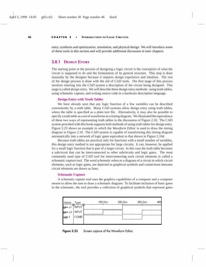
The starting point in the process of designing a logic circuit is the conception of what thecircuit is supposed to do and the formulation of its general structure. This step is donemanually by the designer because it requires design experience and intuition. The restof the design process is done with the aid of CAD tools. The first stage of this processinvolves entering into the CAD system a description of the circuit being designed. Thisstage is calleddesign entry. We will describe three design entry methods: using truth tables,using schematic capture, and writing source code in a hardware description language.
Design Entry with Truth TablesWe have already seen that any logic function of a few variables can be described
conveniently by a truth table. Many CAD systems allow design entry using truth tables,where the table is specified as a plain text file. Alternatively, it may also be possible tospecify a truth table as a set of waveforms in a timing diagram. We illustrated the equivalenceof these two ways of representing truth tables in the discussion of Figure 2.10. The CADsystem provided with this book supports both methods of using truth tables for design entry.Figure 2.23 shows an example in which theWaveform Editoris used to draw the timingdiagram in Figure 2.10. The CAD system is capable of transforming this timing diagramautomatically into a network of logic gates equivalent to that shown in Figure 2.10d.
Because truth tables are practical only for functions with a small number of variables,this design entry method is not appropriate for large circuits. It can, however, be appliedfor a small logic function that is part of a larger circuit. In this case the truth table becomesa subcircuit that can be interconnected to other subcircuits and logic gates. The mostcommonly used type of CAD tool for interconnecting such circuit elements is called aschematic capturetool. The wordschematicrefers to a diagram of a circuit in which circuitelements, such as logic gates, are depicted as graphical symbols and connections betweencircuit elements are drawn as lines.
Schematic CaptureA schematic capture tool uses the graphics capabilities of a computer and a computer
mouse to allow the user to draw a schematic diagram. To facilitate inclusion of basic gatesin the schematic, the tool provides a collection of graphical symbols that represent gates
Figure 2.23 Screen capture of the Waveform Editor.
April 5, 1999 14:05 g02-ch2 Sheet number 31 Page number 47 black
2.8 Introduction to CAD Tools 47
of various types with different numbers of inputs. This collection of symbols is called alibrary. The gates in the library can be imported into the user’s schematic, and the toolprovides a graphical way of interconnecting the gates to create a logic network.
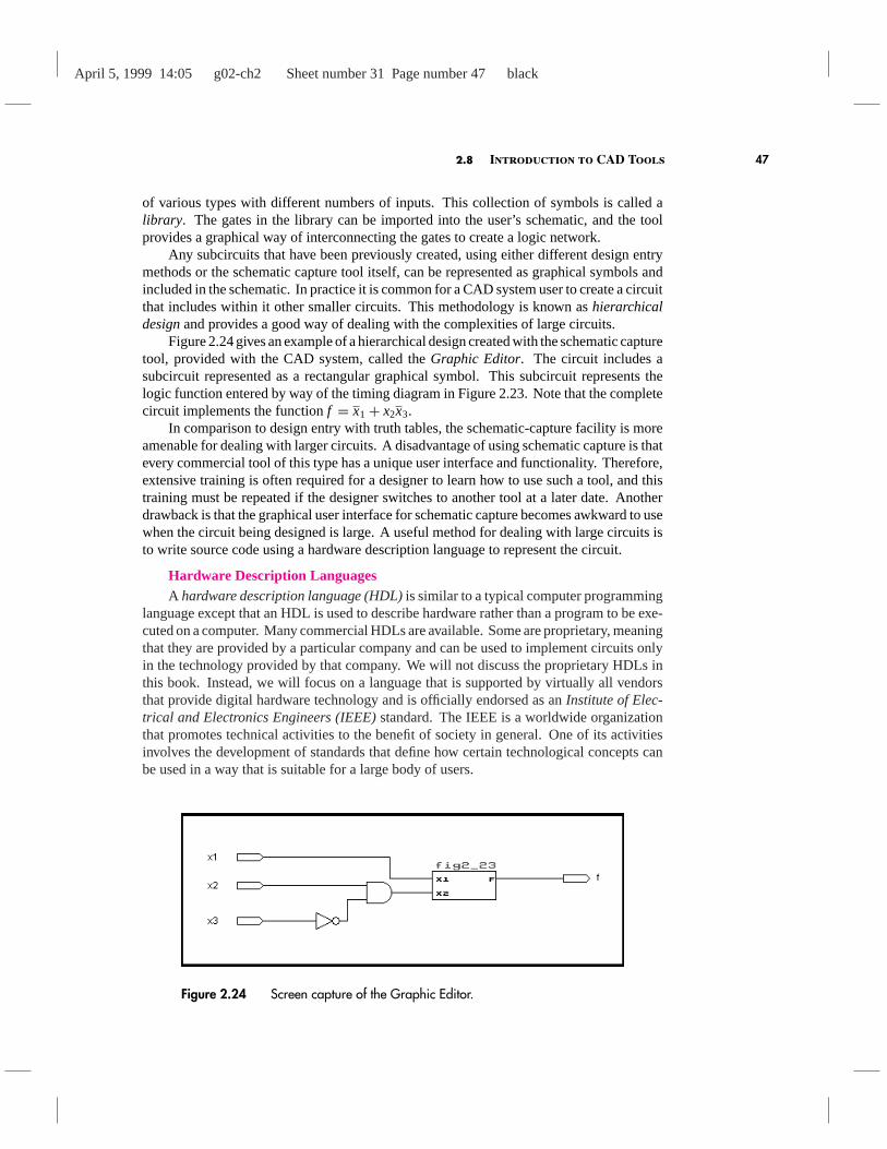
Any subcircuits that have been previously created, using either different design entrymethods or the schematic capture tool itself, can be represented as graphical symbols andincluded in the schematic. In practice it is common for a CAD system user to create a circuitthat includes within it other smaller circuits. This methodology is known ashierarchicaldesignand provides a good way of dealing with the complexities of large circuits.
Figure 2.24 gives an example of a hierarchical design created with the schematic capturetool, provided with the CAD system, called theGraphic Editor. The circuit includes asubcircuit represented as a rectangular graphical symbol. This subcircuit represents thelogic function entered by way of the timing diagram in Figure 2.23. Note that the completecircuit implements the functionf = x1+ x2x3.
In comparison to design entry with truth tables, the schematic-capture facility is moreamenable for dealing with larger circuits. A disadvantage of using schematic capture is thatevery commercial tool of this type has a unique user interface and functionality. Therefore,extensive training is often required for a designer to learn how to use such a tool, and thistraining must be repeated if the designer switches to another tool at a later date. Anotherdrawback is that the graphical user interface for schematic capture becomes awkward to usewhen the circuit being designed is large. A useful method for dealing with large circuits isto write source code using a hardware description language to represent the circuit.
Hardware Description LanguagesA hardware description language (HDL)is similar to a typical computer programming
language except that an HDL is used to describe hardware rather than a program to be exe-cuted on a computer. Many commercial HDLs are available. Some are proprietary, meaningthat they are provided by a particular company and can be used to implement circuits onlyin the technology provided by that company. We will not discuss the proprietary HDLs inthis book. Instead, we will focus on a language that is supported by virtually all vendorsthat provide digital hardware technology and is officially endorsed as anInstitute of Elec-trical and Electronics Engineers (IEEE)standard. The IEEE is a worldwide organizationthat promotes technical activities to the benefit of society in general. One of its activitiesinvolves the development of standards that define how certain technological concepts canbe used in a way that is suitable for a large body of users.
Figure 2.24 Screen capture of the Graphic Editor.
April 5, 1999 14:05 g02-ch2 Sheet number 32 Page number 48 black
48 C H A P T E R 2 • Introduction to Logic Circuits
Two HDLs are IEEE standards:VHDL (Very High Speed Integrated Circuit HardwareDescription Language)and Verilog HDL. Both languages are in widespread use in theindustry. We use VHDL in this book because it is more popular than Verilog HDL. Althoughthe two languages differ in many ways, the choice of using one or the other when studyinglogic circuits is not particularly important, because both offer similar features. Conceptsillustrated in this book using VHDL can be directly applied when using Verilog HDL.
In comparison to performing schematic capture, using VHDL offers a number of ad-vantages. Because it is supported by most companies that offer digital hardware technology,VHDL provides designportability. A circuit specified in VHDL can be implemented in dif-ferent types of chips and with CAD tools provided by different companies, without havingto change the VHDL specification. Design portability is an important advantage becausedigital circuit technology changes rapidly. By using a standard language, the designer canfocus on the required functionality of the desired circuit without being overly concernedabout the details of the technology that will eventually be used for implementation.
Design entry of a logic circuit is done by writing VHDL code. Signals in the circuit arerepresented as variables in the source code, and logic functions are expressed by assigningvalues to these variables. VHDL source code is plain text, which makes it easy for thedesigner to include within the code documentation that explains how the circuit works.This feature, coupled with the fact that VHDL is widely used, encourages sharing and reuseof VHDL-described circuits. This allows faster development of new products in caseswhere existing VHDL code can be adapted for use in the design of new circuits.
Similar to the way in which large circuits are handled in schematic capture, VHDLcode can be written in a modular way that facilitates hierarchical design. Both small andlarge logic circuit designs can be efficiently represented in VHDL code. VHDL has beenused to define circuits such as microprocessors with millions of transistors.
VHDL design entry can be combined with other methods. For example, a schematic-capture tool can be used in which a subcircuit in the schematic is described using VHDL.We will introduce VHDL in section 2.9.
2.8.2 Synthesis
In section 2.4.1 we said that synthesis is the process of generating a logic circuit from atruth table. Synthesis CAD tools perform this process automatically. However, the synthesistools also handle many other tasks. The process oftranslating, or compiling, VHDL codeinto a network of logic gates is part of synthesis.
When the VHDL code representing a circuit is passed through initial synthesis tools,the output is a lower-level description of the circuit. For simplicity we will assume thatthis process produces a set of logic expressions that describe the logic functions needed torealize the circuit. These expressions are then manipulated further by the synthesis tools.If the design entry is performed using schematic capture, then the synthesis tools producea set of logic equations representing the circuit from the schematic diagram. Similarly, iftruth tables are used for design entry, then the synthesis tools generate expressions for thelogic functions represented by the truth tables.
Regardless of what type of design entry is used, the initial logic expressions producedby the synthesis tools are not likely to be in an optimal form. Because these expressions
April 5, 1999 14:05 g02-ch2 Sheet number 33 Page number 49 black
2.8 Introduction to CAD Tools 49
reflect the designer’s input to the CAD tools, it is difficult for a designer to manually produceoptimal results, especially for large circuits. One of the most important tasks of the synthesistools is to manipulate the user’s design to automatically produce an equivalent but bettercircuit. This step of synthesis is calledlogic synthesis, or logic optimization.
The measure of what makes one circuit better than another depends on the particularneeds of a design project and the technology chosen for implementation. In section 2.6we suggested that a good circuit might be one that has the lowest cost. There are otherpossible optimization goals, which are motivated by the type of hardware technology usedfor implementation of the circuit. We will discuss implementation technologies in Chap-ter 3 and return to the issue of optimization goals in Chapter 4.
After logic synthesis the optimized circuit is still represented in the form of logicequations. The final task in the synthesis process is to determine exactly how the circuit willbe realized in a specific hardware technology. This task involves deciding how each logicfunction, represented by an expression, should be implemented using whatever physicalresources are available in the technology. The task involves two steps calledtechnologymapping, followed by layout synthesis, or physical design. We will discuss these steps indetail in Chapter 4.
2.8.3 Functional Simulation
Once the design entry and synthesis are complete, it is useful to verify that the designedcircuit functions as expected. The tool that performs this task is called afunctional simulator,and it uses two types of information. First, the user’s initial design is represented by the logicequations generated during synthesis. Second, the user specifies valuations of the circuit’sinputs that should be applied to these equations during simulation. For each valuation, thesimulator evaluates the outputs produced by the equations. The output of the simulation isprovided either in truth-table form or as a timing diagram. The user examines this outputto verify that the circuit operates as required.
The logic equations used by the simulator are those produced by the synthesis toolsbefore any optimizations are applied during logic synthesis. There would be no advantagein using the optimized form of the equations, because the intent is to evaluate the basicfunctionality of the design, which does not change as a result of optimization. The functionalsimulator assumes that the time needed for signals to propagate through the logic gates isnegligible. In real logic gates this assumption is not realistic, regardless of the hardwaretechnology chosen for implementation of the circuit. However, the functional simulationprovides a first step in validating the basic operation of a design without concern for theeffects of implementation technology. Accurate simulations that account for the timingdetails related to technology can be obtained by using atiming simulator. We will discusstiming simulation in Chapter 4.
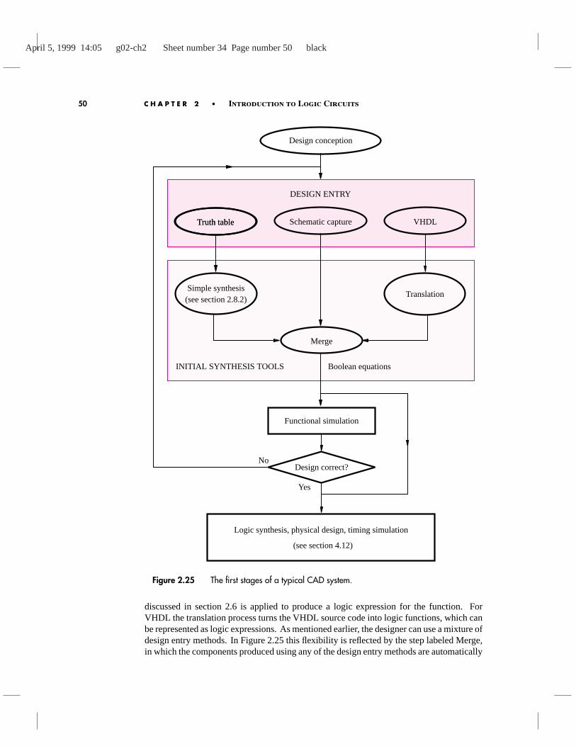
2.8.4 Summary
The CAD tools discussed in this section form a part of a CAD system. A typical design flowthat the user follows is illustrated in Figure 2.25. After the design entry, initial synthesis toolsperform various steps. For a function described by a truth table, the synthesis approach
April 5, 1999 14:05 g02-ch2 Sheet number 34 Page number 50 black
50 C H A P T E R 2 • Introduction to Logic Circuits
Design conception
Truth tableTruth table VHDLSchematic capture
Simple synthesis(see section 2.8.2)
Translation
Merge
Boolean equationsINITIAL SYNTHESIS TOOLS
DESIGN ENTRY
Design correct?
Logic synthesis, physical design, timing simulation
Functional simulation
No
Yes
(see section 4.12)
Figure 2.25 The first stages of a typical CAD system.
discussed in section 2.6 is applied to produce a logic expression for the function. ForVHDL the translation process turns the VHDL source code into logic functions, which canbe represented as logic expressions. As mentioned earlier, the designer can use a mixture ofdesign entry methods. In Figure 2.25 this flexibility is reflected by the step labeled Merge,in which the components produced using any of the design entry methods are automatically
April 5, 1999 14:05 g02-ch2 Sheet number 35 Page number 51 black
2.9 Introduction to VHDL 51
merged into a single design. At this point the circuit is represented in the CAD system asa set of logic equations.
After the initial synthesis the correct operation of the designed circuit can be verified byusing functional simulation. As shown in Figure 2.25, this step is not a requirement in theCAD flow and can be skipped at the designer’s discretion. In practice, however, it is wise toverify that the designed circuit works as expected as early in the design process as possible.Any problems discovered during the simulation are fixed by returning to the design entrystage. Once errors are no longer apparent, the designer proceeds with the remaining toolsin the CAD flow. These include logic synthesis, layout synthesis, timing simulation, andothers. We have mentioned these tools only briefly thus far. The remaining CAD steps willbe described in Chapter 4.
At this point the reader should have some appreciation for what is involved when usingCAD tools. However, the tools can be fully appreciated only when they are used firsthand.In Appendexes B to D, we provide step-by-step tutorials that illustrate how to use theMAX+plusII CAD system, which is included with this book. The tutorial in Appendix Bcovers design entry with both schematic capture and VHDL, as well as functional simulation.We strongly encourage the reader to work through the hands-on material. Because thetutorial uses VHDL for design entry, we provide an introduction to VHDL in the followingsection.
2.9 Introduction to VHDL
In the 1980s rapid advances in integrated circuit technology lead to efforts to developstandard design practices for digital circuits. VHDL was developed as a part of that effort.VHDL has become the industry standard language for describing digital circuits, largelybecause it is an official IEEE standard. The original standard for VHDL was adopted in1987 and called IEEE 1076. A revised standard was adopted in 1993 and called IEEE 1164.
VHDL was originally intended to serve two main purposes. First, it was used as adocumentation language for describing the structure of complex digital circuits. As anofficial IEEE standard, VHDL provided a common way of documenting circuits designedby numerous designers. Second, VHDL provided features for modeling the behavior of adigital circuit, which allowed its use as input to software programs that were then used tosimulate the circuit’s operation.
In recent years, in addition to its use for documentation and simulation, VHDL hasalso become popular for use in design entry in CAD systems. The CAD tools are used tosynthesize the VHDL code into a hardware implementation of the described circuit. In thisbook our main use of VHDL will be for synthesis.
VHDL is an extremely complex, sophisticated language. Learning all of its features isa daunting task. However, for use in synthesis only a subset of these features is important.To avoid confusion in learning this complex language, we will discuss only the features ofVHDL that are actually used in the examples in the book. The material presented shouldbe sufficient to allow the reader to design a wide range of circuits. The reader who wishesto learn the complete VHDL language can refer to one of the specialized texts [4–8].
To further simplify the task of learning VHDL, we will introduce the language inseveral stages throughout the book. Our general approach will be to introduce particularfeatures only when they are relevant to the design topics covered in that part of the text. For
April 5, 1999 14:05 g02-ch2 Sheet number 36 Page number 52 black
52 C H A P T E R 2 • Introduction to Logic Circuits
convenience, in Appendix A we provide a complete listing of the VHDL features covered inthe book. The reader may wish to refer to that material from time to time. In the remainderof this section, we discuss the most basic concepts needed to write simple VHDL code.
2.9.1 Representation of Digital Signals in VHDL
When using CAD tools to synthesize a logic circuit, the designer can provide the initialdescription of the circuit in several different ways, as we explained in section 2.8.1. Oneconvenient way is to write this description in the form of VHDL source code. The VHDLcompiler translates this code into a logic circuit. Each logic signal in the circuit is representedin VHDL code as a data object. Just as the variables declared in any high-level programminglanguage have associated types, such as integers or characters, data objects in VHDL can beof various types. The original VHDL standard, IEEE 1076, includes a data type calledBIT.An object of this type is well suited for representing digital signals because BIT objects canhave only two values, 0 and 1. In this chapter all signals in our examples will be of typeBIT. Other data types are introduced in section 4.11 and are listed in Appendix A.
2.9.2 Writing Simple VHDL Code
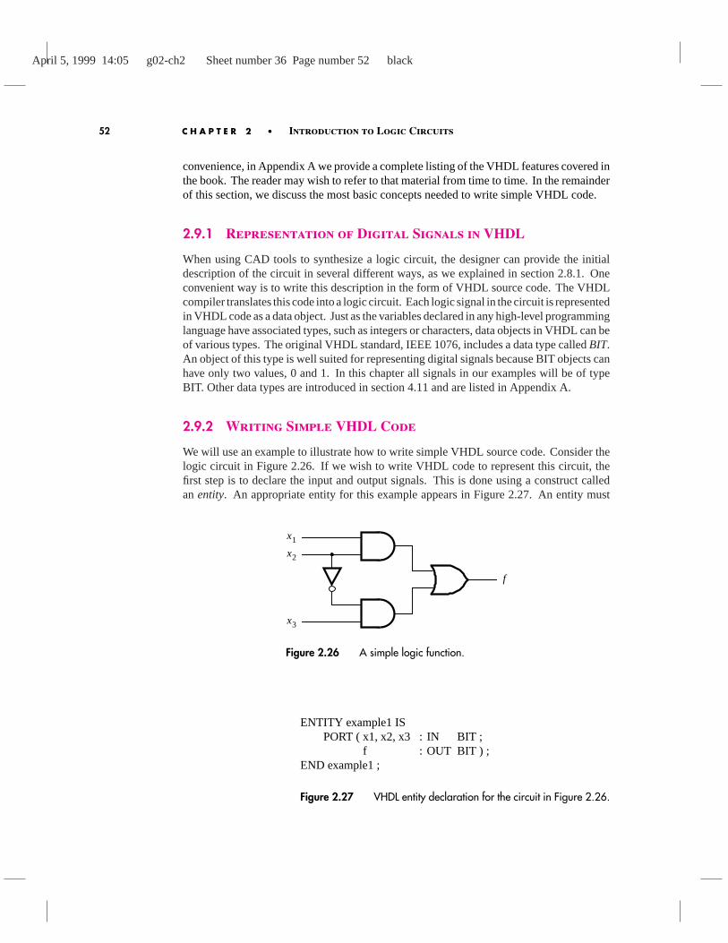
We will use an example to illustrate how to write simple VHDL source code. Consider thelogic circuit in Figure 2.26. If we wish to write VHDL code to represent this circuit, thefirst step is to declare the input and output signals. This is done using a construct calledanentity. An appropriate entity for this example appears in Figure 2.27. An entity must
f
x3
x1
x2
Figure 2.26 A simple logic function.
ENTITY example1 ISPORT ( x1, x2, x3 : IN BIT ;
f : OUT BIT ) ;END example1 ;
Figure 2.27 VHDL entity declaration for the circuit in Figure 2.26.

April 5, 1999 14:05 g02-ch2 Sheet number 37 Page number 53 black
2.9 Introduction to VHDL 53
be assigned a name; we have chosen the nameexample1for this first example. The inputand output signals for the entity are called itsports, and they are identified by the keywordPORT. This name derives from the electrical jargon in which the wordport refers to aninput or output connection to an electronic circuit. Each port has an associatedmodethatspecifies whether it is an input (IN) to the entity or an output (OUT) from the entity. Eachport represents a signal, hence it has an associated type. The entityexample1has four portsin total. The first three,x1, x2, andx3, are input signals of type BIT. The port namedf is anoutput of type BIT.
In Figure 2.27 we have used simple signal namesx1, x2, x3, andf for the entity’s ports.Similar to most computer programming languages, VHDL has rules that specify whichcharacters are allowed in signal names. A simple guideline is that signal names can includeany letter or number, as well as the underscore character ‘_’. There are two caveats: asignal name must begin with a letter, and a signal name cannot be a VHDL keyword.
An entity specifies the input and output signals for a circuit, but it does not give anydetails as to what the circuit represents. The circuit’s functionality must be specified with aVHDL construct called anarchitecture. An architecture for our example appears in Figure2.28. It must be given a name, and we have chosen the nameLogicFunc. Although the namecan be any text string, it is sensible to assign a name that is meaningful to the designer.In this case we have chosen the nameLogicFuncbecause the architecture specifies thefunctionality of the design using a logic expression. VHDL has built-in support for thefollowing Boolean operators: AND, OR, NOT, NAND, NOR, XOR, and XNOR. (So farwe have introduced only AND, OR, and NOT operators; the others will be presented inChapter 3.) Following the BEGIN keyword, our architecture specifies, using the VHDLsignal assignment operator<=, that outputf should be assigned the result of the logicexpression on the right-hand side of the operator. Because VHDL does not assume anyprecedence of logic operators, parentheses are used in the expression. One might expectthat an assignment statement such as
f <= x1 AND x2 OR NOTx2 AND x3
would have implied parentheses
f <= (x1 AND x2) OR ((NOT x2) AND x3)
But for VHDL code this assumption is not true. In fact, without the parentheses the VHDLcompiler would produce a compile-time error for this expression.
Complete VHDL code for our example is given in Figure 2.29. This example hasillustrated that a VHDL source code file has two main sections: an entity and an architecture.
ARCHITECTURE LogicFunc OF example1 ISBEGIN
f <= (x1 AND x2) OR (NOT x2 AND x3) ;END LogicFunc ;
Figure 2.28 VHDL architecture for the entity in Figure 2.27.

April 5, 1999 14:05 g02-ch2 Sheet number 38 Page number 54 black
54 C H A P T E R 2 • Introduction to Logic Circuits
ENTITY example1 ISPORT ( x1, x2, x3 : IN BIT ;
f : OUT BIT ) ;END example1 ;
ARCHITECTURE LogicFunc OF example1 ISBEGIN
f <= (x1 AND x2) OR (NOT x2 AND x3) ;END LogicFunc ;
Figure 2.29 Complete VHDL code for the circuit in Figure 2.26.
A simple analogy for what each section represents is that the entity is equivalent to a symbolin a schematic diagram and the architecture specifies the logic circuitry inside the symbol.
A second example of VHDL code is given in Figure 2.30. This circuit has four inputsignals, calledx1,x2,x3, andx4, and two output signals, namedf andg. A logic expressionis assigned to each output. A logic circuit produced by the VHDL compiler for this exampleis shown in Figure 2.31.
The preceding two examples indicate that one way to assign a value to a signal inVHDL code is by means of a logic expression. In VHDL terminology a logic expressionis called asimple assignment statement. We will see later that VHDL also supports severalother types of assignment statements and many other features that are useful for describingcircuits that are much more complex.
2.9.3 How NOT to Write VHDL Code
When learning how to use VHDL or other hardware description languages, the tendency forthe novice is to write code that resembles a computer program, containing many variables
ENTITY example2 ISPORT ( x1, x2, x3, x4 : IN BIT ;
f, g : OUT BIT ) ;END example2 ;
ARCHITECTURE LogicFunc OF example2 ISBEGIN
f <= (x1 AND x3) OR (NOT x3 AND x2) ;g<= (NOT x3 OR x1) AND (NOT x3 OR x4) ;
END LogicFunc ;
Figure 2.30 VHDL code for a four-input function.
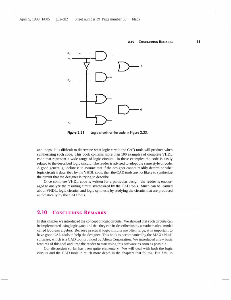
April 5, 1999 14:05 g02-ch2 Sheet number 39 Page number 55 black
2.10 Concluding Remarks 55
f
g
x3
x1
x2
x4
Figure 2.31 Logic circuit for the code in Figure 2.30.
and loops. It is difficult to determine what logic circuit the CAD tools will produce whensynthesizing such code. This book contains more than 100 examples of complete VHDLcode that represent a wide range of logic circuits. In these examples the code is easilyrelated to the described logic circuit. The reader is advised to adopt the same style of code.A good general guideline is to assume that if the designer cannot readily determine whatlogic circuit is described by the VHDL code, then the CAD tools are not likely to synthesizethe circuit that the designer is trying to describe.
Once complete VHDL code is written for a particular design, the reader is encour-aged to analyze the resulting circuit synthesized by the CAD tools. Much can be learnedabout VHDL, logic circuits, and logic synthesis by studying the circuits that are producedautomatically by the CAD tools.
2.10 Concluding Remarks
In this chapter we introduced the concept of logic circuits. We showed that such circuits canbe implemented using logic gates and that they can be described using a mathematical modelcalled Boolean algebra. Because practical logic circuits are often large, it is important tohave good CAD tools to help the designer. This book is accompanied by the MAX+PlusIIsoftware, which is a CAD tool provided by Altera Corporation. We introduced a few basicfeatures of this tool and urge the reader to start using this software as soon as possible.
Our discussion so far has been quite elementary. We will deal with both the logiccircuits and the CAD tools in much more depth in the chapters that follow. But first, in
April 5, 1999 14:05 g02-ch2 Sheet number 40 Page number 56 black
56 C H A P T E R 2 • Introduction to Logic Circuits
Chapter 3 we will examine the most important electronic technologies used to constructlogic circuits. This material will give the reader an appreciation of practical constraints thata designer of logic circuits must face.
Problems
2.1 Use algebraic manipulation to prove thatx+ yz= (x+ y) · (x+ z). Note that this is thedistributive rule, as stated in identity 12b in section 2.5.
2.2 Use algebraic manipulation to prove that(x+ y) · (x+ y) = x.
2.3 Use the Venn diagram to prove the identity in problem 1.
2.4 Use the Venn diagram to prove DeMorgan’s theorem, as given in expressions 15a and 15bin section 2.5.
2.5 Use the Venn diagram to prove
(x1+ x2 + x3) · (x1+ x2 + x3) = x1+ x2
2.6 Determine whether or not the following expressions are valid, i.e., whether the left- andright-hand sides represent same function.(a)x1x3+ x1x2x3+ x1x2 + x1x2 = x2x3+ x1x3+ x2x3+ x1x2x3
(b) x1x3+ x2x3+ x2x3 = (x1+ x2 + x3)(x1+ x2 + x3)(x1+ x2 + x3)
(c) (x1+ x3)(x1+ x2 + x3)(x1+ x2) = (x1+ x2)(x2 + x3)(x1+ x3)
2.7 Draw a timing diagram for the circuit in Figure 2.19a. Show the waveforms that can beobserved on all wires in the circuit.
2.8 Repeat problem 2.7 for the circuit in Figure 2.19b.
2.9 Use algebraic manipulation to show that for three input variablesx1, x2, andx3∑m(1, 2, 3, 4, 5, 6, 7) = x1+ x2 + x3
2.10 Use algebraic manipulation to show that for three input variablesx1, x2, andx3
5 M(0, 1, 2, 3, 4, 5, 6) = x1x2x3
2.11 Use algebraic manipulation to find the minimum sum-of-products expression for the func-tion f = x1x3+ x1x2 + x1x2x3+ x1x2x3.
2.12 Use algebraic manipulation to find the minimum sum-of-products expression for the func-tion f = x1x2x3+ x1x2x4 + x1x2x3x4.
2.13 Use algebraic manipulation to find the minimum product-of-sums expression for the func-tion f = (x1+ x3+ x4) · (x1+ x2 + x3) · (x1+ x2 + x3+ x4).
2.14 Use algebraic manipulation to find the minimum product-of-sums expression for the func-tion f = (x1+ x2 + x3) · (x1+ x2 + x3) · (x1+ x2 + x3) · (x1+ x2 + x3).
2.15 (a) Show the location of all minterms in a three-variable Venn diagram.
April 5, 1999 14:05 g02-ch2 Sheet number 41 Page number 57 black
Problems 57
(b) Show a separate Venn diagram for each product term in the functionf = x1x2x3+x1x2+x1x3. Use the Venn diagram to find the minimal sum-of-products form off.
2.16 Represent the function in Figure 2.18 in the form of a Venn diagram and find its minimalsum-of-products form.
2.17 Figure P2.1 shows two attempts to draw a Venn diagram for four variables. For parts (a)and (b) of the figure, explain why the Venn diagram is not correct. (Hint: the Venn diagrammust be able to represent all 16 minterms of the four variables.)
x1 x2
x3
x4
(a)
x1 x2
x3
x4
(b)
Figure P2.1 Two attempts to draw a four-variable Venn diagram.
2.18 Figure P2.2 gives a representation of a four-variable Venn diagram and shows the locationof mintermsm0,m1, andm2. Show the location of the other minterms in the diagram.Represent the functionf = x1x2x3x4 + x1x2x3x4 + x1x2 on this diagram.
x3
x2x1
x4
x3
x2x1
m0
m1m2
Figure P2.2 A four-variable Venn diagram.
2.19 Design the simplest sum-of-products circuit that implements the functionf (x1, x2, x3) =∑m(3, 4, 6, 7).
2.20 Design the simplest sum-of-products circuit that implements the functionf (x1, x2, x3) =∑m(1, 3, 4, 6, 7).
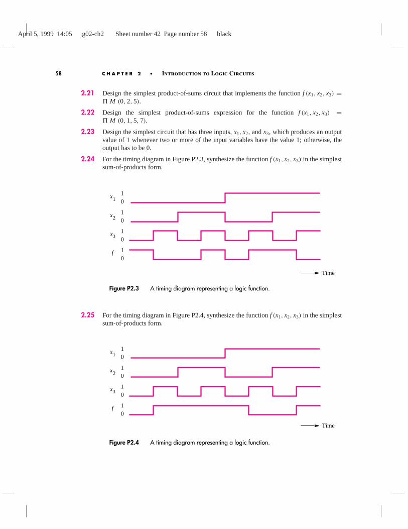
April 5, 1999 14:05 g02-ch2 Sheet number 42 Page number 58 black
58 C H A P T E R 2 • Introduction to Logic Circuits
2.21 Design the simplest product-of-sums circuit that implements the functionf (x1, x2, x3) =5 M (0, 2, 5).
2.22 Design the simplest product-of-sums expression for the functionf (x1, x2, x3) =5 M (0, 1, 5, 7).
2.23 Design the simplest circuit that has three inputs,x1, x2, andx3, which produces an outputvalue of 1 whenever two or more of the input variables have the value 1; otherwise, theoutput has to be 0.
2.24 For the timing diagram in Figure P2.3, synthesize the functionf (x1, x2, x3) in the simplestsum-of-products form.
10
10
10
10
x1
x2
Time
x3
f
Figure P2.3 A timing diagram representing a logic function.
2.25 For the timing diagram in Figure P2.4, synthesize the functionf (x1, x2, x3) in the simplestsum-of-products form.
10
10
10
10
x1
x2
Time
x3
f
Figure P2.4 A timing diagram representing a logic function.
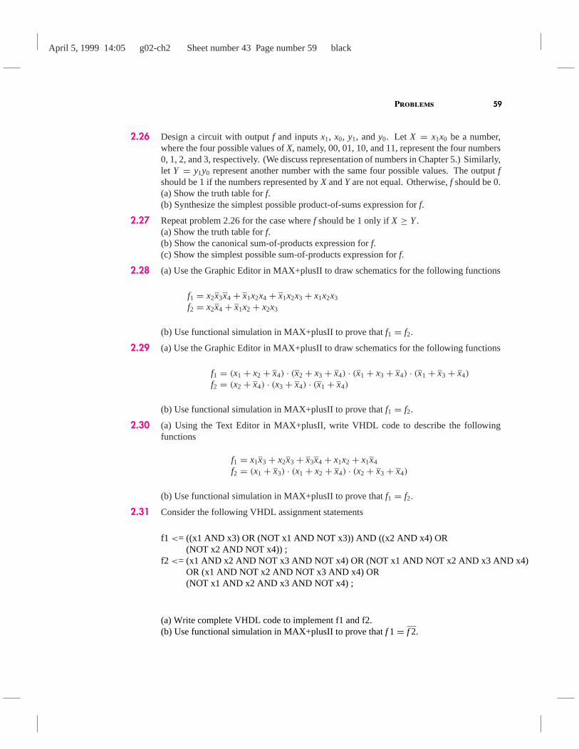
April 5, 1999 14:05 g02-ch2 Sheet number 43 Page number 59 black
Problems 59
2.26 Design a circuit with outputf and inputsx1, x0, y1, andy0. Let X = x1x0 be a number,where the four possible values ofX, namely, 00, 01, 10, and 11, represent the four numbers0, 1, 2, and 3, respectively. (We discuss representation of numbers in Chapter 5.) Similarly,let Y = y1y0 represent another number with the same four possible values. The outputfshould be 1 if the numbers represented byX andYare not equal. Otherwise,f should be 0.(a) Show the truth table forf.(b) Synthesize the simplest possible product-of-sums expression forf.
2.27 Repeat problem 2.26 for the case wheref should be 1 only ifX ≥ Y.(a) Show the truth table forf.(b) Show the canonical sum-of-products expression forf.(c) Show the simplest possible sum-of-products expression forf.
2.28 (a) Use the Graphic Editor in MAX+plusII to draw schematics for the following functions
f1 = x2x3x4 + x1x2x4 + x1x2x3+ x1x2x3
f2 = x2x4 + x1x2 + x2x3
(b) Use functional simulation in MAX+plusII to prove thatf1 = f2.
2.29 (a) Use the Graphic Editor in MAX+plusII to draw schematics for the following functions
f1 = (x1+ x2 + x4) · (x2 + x3+ x4) · (x1+ x3+ x4) · (x1+ x3+ x4)
f2 = (x2 + x4) · (x3+ x4) · (x1+ x4)
(b) Use functional simulation in MAX+plusII to prove thatf1 = f2.
2.30 (a) Using the Text Editor in MAX+plusII, write VHDL code to describe the followingfunctions
f1 = x1x3+ x2x3+ x3x4 + x1x2 + x1x4
f2 = (x1+ x3) · (x1+ x2 + x4) · (x2 + x3+ x4)
(b) Use functional simulation in MAX+plusII to prove thatf1 = f2.
2.31 Consider the following VHDL assignment statements
f1 <= ((x1 AND x3) OR (NOT x1 AND NOT x3)) AND ((x2 AND x4) OR(NOT x2 AND NOT x4)) ;
f2 <= (x1 AND x2 AND NOT x3 AND NOT x4) OR (NOT x1 AND NOT x2 AND x3 AND x4)OR (x1 AND NOT x2 AND NOT x3 AND x4) OR(NOT x1 AND x2 AND x3 AND NOT x4) ;
(a) Write complete VHDL code to implement f1 and f2.(b) Use functional simulation in MAX+plusII to prove thatf 1= f 2.

April 5, 1999 14:05 g02-ch2 Sheet number 44 Page number 60 black
60 C H A P T E R 2 • Introduction to Logic Circuits
References
1. G. Boole,An Investigation of the Laws of Thought, 1854, reprinted by DoverPublications, New York, 1954.
2. C. E. Shannon, “A Symbolic Analysis of Relay and Switching Circuits,”Transactionsof AIEE57 (1938), pp. 713–723.
3. E. V. Huntington, “Sets of Independent Postulates for the Algebra of Logic,”Transactions of the American Mathematical Society5 (1904), pp. 288–309.
4. Z. Navabi,VHDL—Analysis and Modeling of Digital Systems, 2nd ed.(McGraw-Hill: New York, 1998).
5. D. L. Perry,VHDL, 3rd ed. (McGraw-Hill: New York, 1998).
6. J. Bhasker,A VHDL Primer(Prentice-Hall: Englewood Cliffs, NJ, 1995).
7. K. Skahill,VHDL for Programmable Logic(Addison-Wesley: Menlo Park, CA,1996).
8. A. Dewey,Analysis and Design of Digital Systems with VHDL(PWS Publishing Co.:Boston, 1997).