Embed Size (px)
Citation preview

Organic Electronic, Fall 2005, Dr. Dietmar Knipp
Structural properties and electronic transport
Information:http://www.faculty.iu-bremen.de/course/c300331a/
Source: Apple
Ref.: Apple
Information:http://www.faculty.iu-bremen.de/course/c420411/
Dielectric
e e e e e e e e
Gate
VGNeutral substrate
Source Drain
VD
h h h h h h h h h h
101110-110-210-310-410-510-610-8
Critical dimension (m)10-710-9
Introduction to Organic Electronics(Nanomolecular Science Seminar I)(Course Number 420411 ) Fall 2005
Organic materials and electronic Transport
Instructor: Dr. Dietmar Knipp

Organic Electronic, Fall 2005, Dr. Dietmar Knipp
Structural properties and electronic transport
Introduction to Organic Electronics
2 Structural properties and Electronic Transport2.1 General properties of organic and polymeric semiconducting material2.2 Organic and polymeric semiconducting materials2.3 Organic molecules2.4 From a single molecule to a solid2.5 Bandgap in organic solids2.6 Structural order of materials2.7 The unit cell2.8 Structural order in molecular solids2.9 Electronic Transport
2.9.1 Thermal movement of carriers2.9.2 Band-like transport2.9.3 Grain boundaries in polycrystalline material2.9.4 Trap-controlled transport2.9.5 Hopping transport
References

Organic Electronic, Fall 2005, Dr. Dietmar Knipp
Structural properties and electronic transport
2.1 General properties of organic and polymeric semiconducting materials
Advantages:
•Low cost processing
•Large area compatible
•Low temperature processing
•Tailoring of electronic and optical properties
•Certain properties not easily attainable with conventional materials
Disadvantages:
•Low carrier mobility
•Stability
•Patterning of films
•Novel fabrication technology required
Tetracene

Organic Electronic, Fall 2005, Dr. Dietmar Knipp
Structural properties and electronic transport
2.2 Organic and polymeric semiconducting materialsTwo general classes of materials exist:
Antracene
Tetracene
Pentacene
Phthalocyanine
N
N
N
N
N
N
N
N
M
Organic molecules
Perylene
SS
C8 C8
poly(9,9-dioctylfluorene-co-bithiophene) (F8T2)
Polymers
Poly(3-hexyl thiophene) (P3HT)
XPT: regio-regular poly(thiophene)

Organic Electronic, Fall 2005, Dr. Dietmar Knipp
Structural properties and electronic transport
2.3 Organic Molecules
Hydrocarbons, the simplest organic molecules, contain only carbon and hydrogen atoms. They can be subdivided in Alkanes, Alkenes, Alkynes, Arenes.
Arenes and AromaticityArenes are hydrocarbons based on benzene units. The simplest, yet the most important compound in this class of organic compounds is benzene.
"Aromatic" was originally used to describe these compounds since many have pleasent smells. To the chemist, the word aromatic also carries with it stabilityand reactivity implications. The unusual stability of benzene compared to closely related alkenes is what makes it important and gives benzene its own set of characteristic reactions.
Organic Electronic, Fall 2005, Dr. Dietmar Knipp
Structural properties and electronic transport
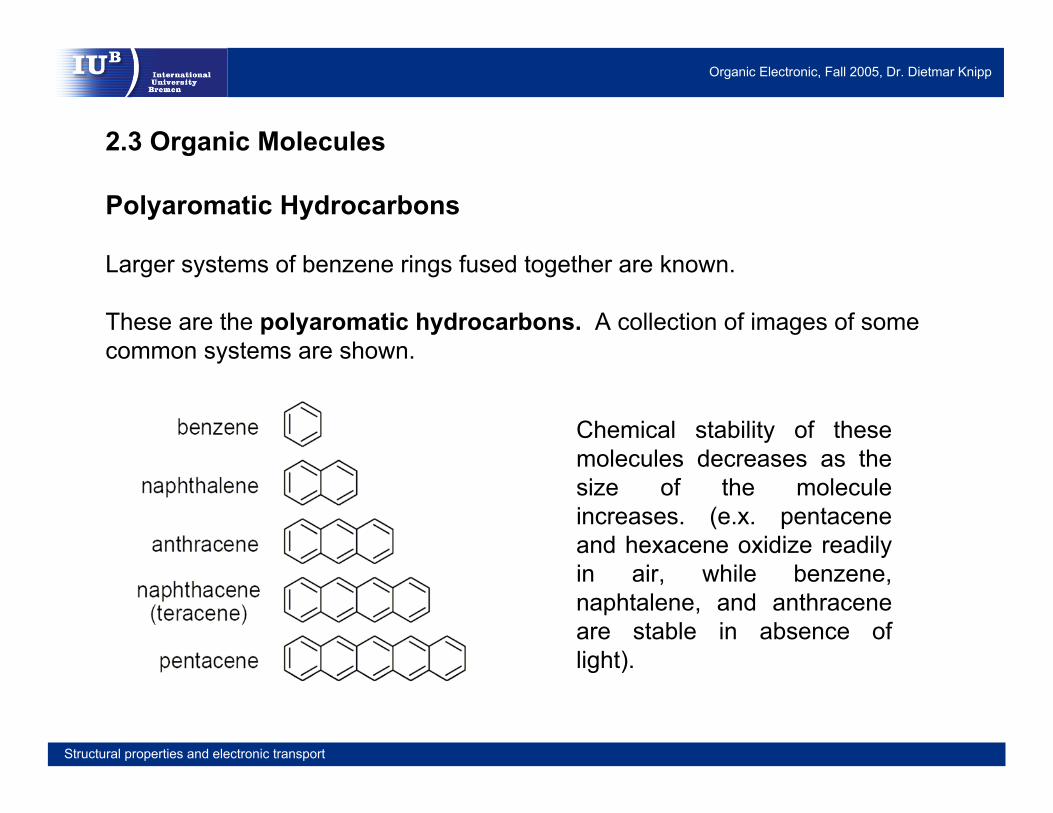
2.3 Organic Molecules
Polyaromatic Hydrocarbons
Larger systems of benzene rings fused together are known.
These are the polyaromatic hydrocarbons. A collection of images of some common systems are shown.
Chemical stability of these molecules decreases as the size of the molecule increases. (e.x. pentacene and hexacene oxidize readily in air, while benzene, naphtalene, and anthraceneare stable in absence of light).

Organic Electronic, Fall 2005, Dr. Dietmar Knipp
Structural properties and electronic transport
π-electron overlap between adjacent carbon atoms: leads to delocalization
Within a single molecule there is very good electronic overlap
pi molecular orbitals for benzene. With 6 C atoms contributing to the p system, we need to create 6 molecular orbitals.
2.3 Organic MoleculesEnergy distribution of Benzene
Ref.: I. Hunt, University of Calgary
Organic Electronic, Fall 2005, Dr. Dietmar Knipp
Structural properties and electronic transport
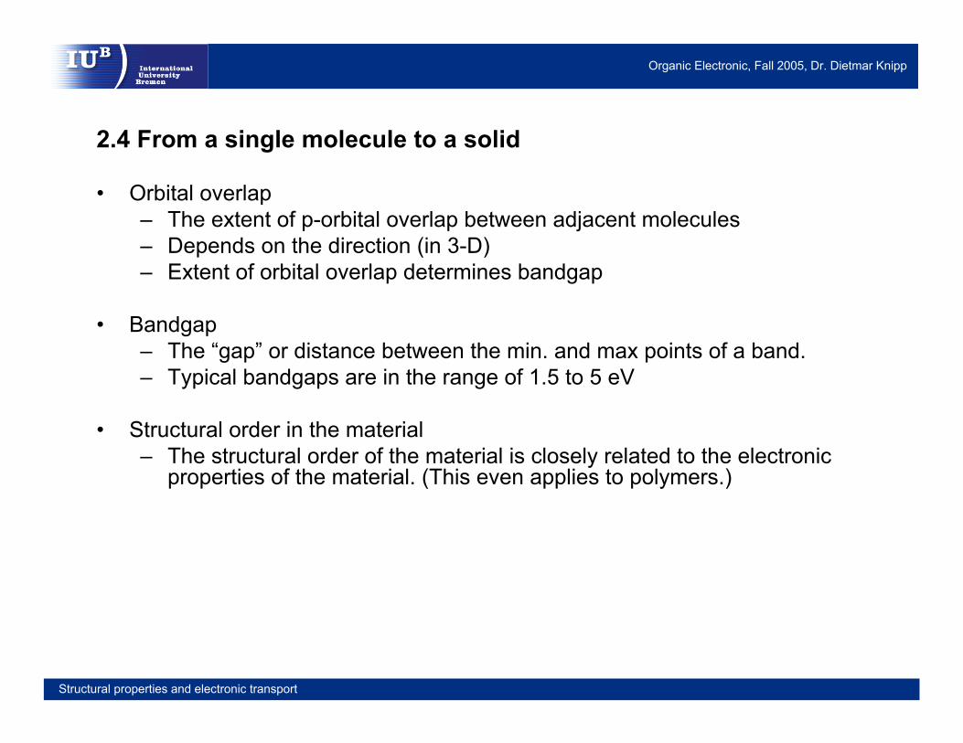
2.4 From a single molecule to a solid
• Orbital overlap– The extent of p-orbital overlap between adjacent molecules– Depends on the direction (in 3-D)– Extent of orbital overlap determines bandgap
• Bandgap– The “gap” or distance between the min. and max points of a band. – Typical bandgaps are in the range of 1.5 to 5 eV
• Structural order in the material– The structural order of the material is closely related to the electronic
properties of the material. (This even applies to polymers.)

Organic Electronic, Fall 2005, Dr. Dietmar Knipp
Structural properties and electronic transport
2.5 Bandgap in organic solids
Electronic states given rise to valence (HOMO level) and conduction bands (LUMO level). The bands are shown for a series of materials from benzene to pentacene. The dashed line corresponds to the Fermi level. The electronic states are given for the gas phase and a solid. Ref.: N. Karl, University Stuttgart

Organic Electronic, Fall 2005, Dr. Dietmar Knipp
Structural properties and electronic transport
Amorphous materials
Poly crystallinematerials
(Mono)Crystallinematerials
No long-range order
Completely ordered in segments
Entirely ordered solid
Ref.: R.F. Pierret, Semiconductor Fundamentals
The structural properties of organic solid depends on the molecule itself, its electrical structure, the substrate and the growth conditions (temperature, deposition rate, flow of material) or preparation conditions.
2.5 Structural order of materials

Organic Electronic, Fall 2005, Dr. Dietmar Knipp
Structural properties and electronic transport
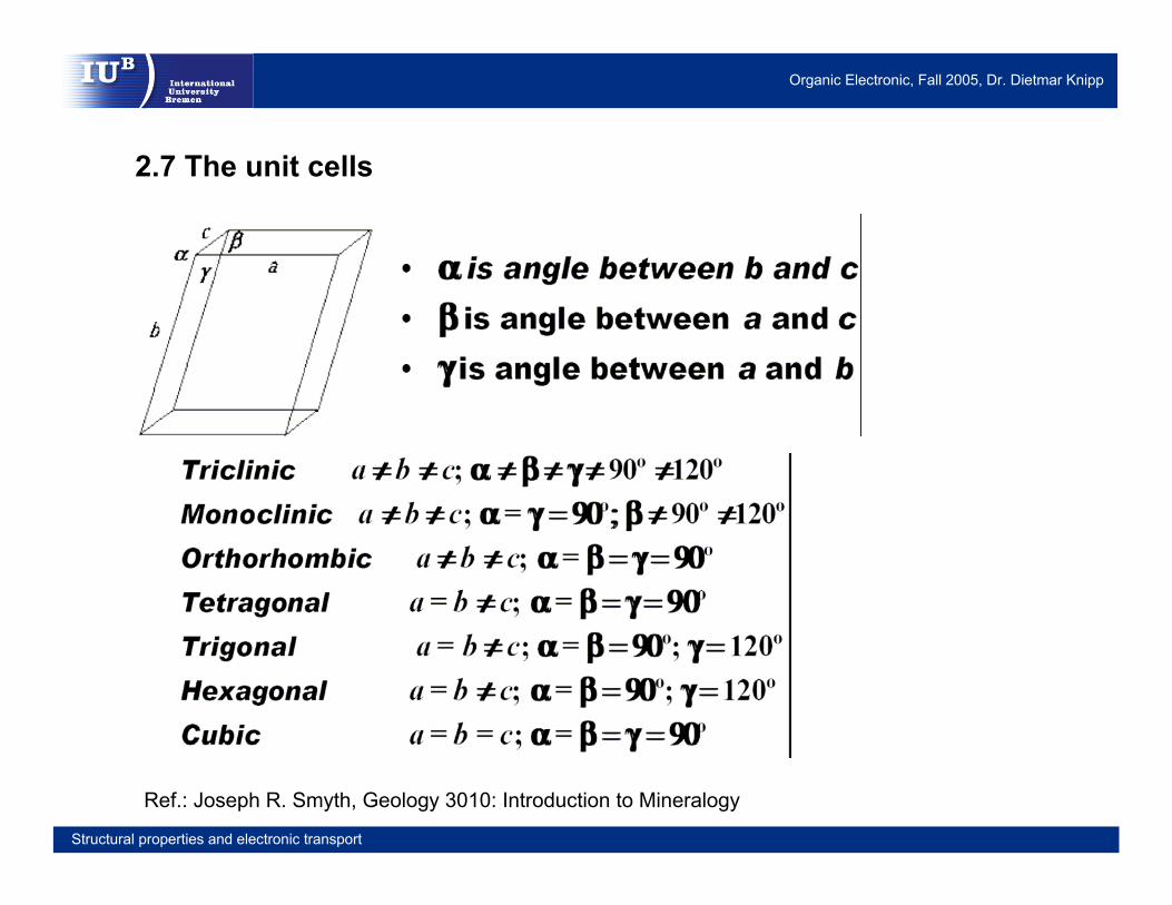
2.7 The unit cell
The periodic arrangement of atoms is called lattice!
A unit cell of a material represents the entire lattice. By repeating the unit cell throughout the crystal, one can generate the entire lattice.
A unit cell can be characterized by a vector R, where a, b and c are vectors and m, n and p are integers, so that each point of a lattice can be found.
R=ma+nb+pc
The vectors a, b, and c are called the lattice constants.
Primitive unit cell.
Ref.: M.S. Sze, Semiconductor Devices

Organic Electronic, Fall 2005, Dr. Dietmar Knipp
Structural properties and electronic transport
2.7 The unit cell
Different unit cells based on cubic unit cells
Ref.: M.S. Sze, Semiconductor Devices
Simple cubic unit
cell
Body centered cubic unit cell
(bcc)
Face centered cubic unit cell
(fcc)
Organic Electronic, Fall 2005, Dr. Dietmar Knipp
Structural properties and electronic transport
2.7 The unit cells
Ref.: Joseph R. Smyth, Geology 3010: Introduction to Mineralogy
Organic Electronic, Fall 2005, Dr. Dietmar Knipp
Structural properties and electronic transport
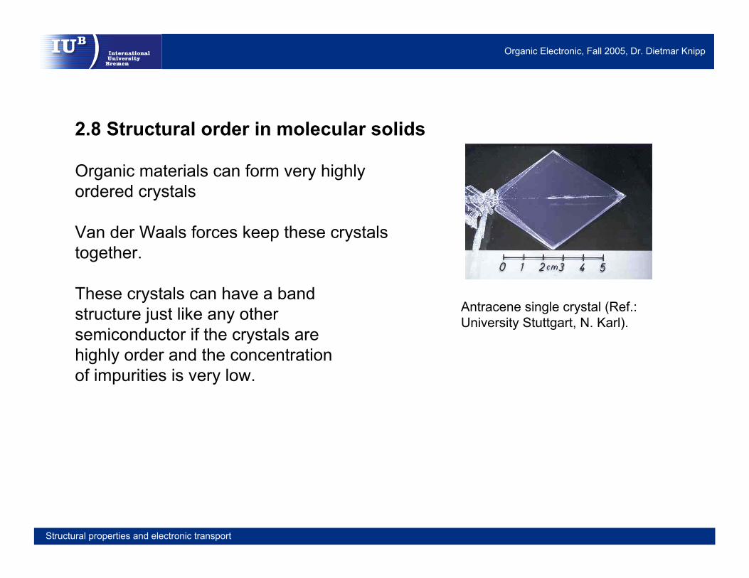
2.8 Structural order in molecular solids
Organic materials can form very highlyordered crystals
Van der Waals forces keep these crystalstogether.
These crystals can have a bandstructure just like any othersemiconductor if the crystals are highly order and the concentration of impurities is very low.
Antracene single crystal (Ref.: University Stuttgart, N. Karl).

Organic Electronic, Fall 2005, Dr. Dietmar Knipp
Structural properties and electronic transport
Electronic transport due to an overlap of π−orbitals
Thermal Evaporation: Source temperature: 275-300°C
Material: 0, 1 or 2 times sublimation purified
Substrate temperature: rt-110°C
a
c
bα
β
γ
Pentacene, C22H14 :
Aromatic hydrocarbons based on linear arranged benzene rings
Crystal structure: Triclinic: a ≠ b ≠ c, α ≠ β ≠ γ ≠ 90°
Substrate view
2.8 Structural order in molecular solids

Organic Electronic, Fall 2005, Dr. Dietmar Knipp
Structural properties and electronic transport
Substrate temperature
2.5µm 2.5µm2.5µm
Pentacene on thermal oxide
Substrate at rt Substrate at 70°C Substrate at 90°C
Crystal size
Atomic force micrographs of thermally evaporated pentacene films (200nm).
2.8 Structural order in molecular solids

Organic Electronic, Fall 2005, Dr. Dietmar Knipp
Structural properties and electronic transport
X-ray diffraction pattern of pentacene on thermal oxide
0
15
30
45
60
75
90
10 20 30
(003)17.22°
(002)11.46°
(001)5.743°
2 Θ scan
16°
Substrate view
Diff
ract
ion
inte
nsity
[a.u
.]
The pentacene film was prepared at room temperature.
2.8 Structural order in molecular solids

Organic Electronic, Fall 2005, Dr. Dietmar Knipp
Structural properties and electronic transport
0.01
0.1
1
0.1 1 10
room temperature70°C90°C
Rat
io o
f x-ra
y di
ffrac
tion
(001
)/(00
1‘)
average crystal size [µm]
X-ray diffraction pattern of pentacene on thermal oxide
Relation between the average crystal size and the ratio of the diffraction peaks.
2.8 Structural order in molecular solids

Organic Electronic, Fall 2005, Dr. Dietmar Knipp
Structural properties and electronic transport
2.9 Electronic Transport
The structural order of the material is closely related to the electronic properties of the material.
Structural Order10-6
10-4
10-2
100
Mob
ility
[cm
2 /Vs]
Band-like transport
Hopping transport
Disorder
Grain boundaries or trap-controlled
transport
- Transistors High mobility materials and its appications
Low mobility materials and its applications- Photoconductors- Organic LEDs

Organic Electronic, Fall 2005, Dr. Dietmar Knipp
Structural properties and electronic transport
2.9 Electronic TransportElectrons in the conduction band and holes in the valence band are able to move upon thermal activation, a gradient or an applied electric field. In the following the concepts of electronic transport in crystalline materials will be described.
2.9.1 Thermal movement of carriersElectrons in the conduction or holes in the valence band can essentially be treated as free carriers or free particles. Even in the absence of an electric field the carriers follow a thermally activated random motion. In thermal equilibrium the average thermal energy of a particle (electron or hole) can be obtained from the theorem for equipartition of
The thermal energy of the particle is equal to the kinetic energy of the electron, so that the velocity of the particle can be calculated. The mass of the electron is equal to the effective mass of the electron.
kTEthermalaverage 23
= Average thermal energy of an electron / hole

Organic Electronic, Fall 2005, Dr. Dietmar Knipp
Structural properties and electronic transport
2.9.1 Thermal movement of carriers
Furthermore, the velocity of the electron corresponds to the thermal velocity of the electron, so that the thermal velocity can be determined by:
At room temperature the average thermal velocity of an electron is about 105m/s in silicon and GaAs.
Thermal motion of free carriers can be seen as random collision (scattering) of the free carriers with the crystal lattice. A random motion of an electron or hole leads to zero net displacement of the free carrier over a sufficient long distance / period of time. The average distance between two collisions within the crystal lattice is called mean free path. Associated to the mean free pathwe can introduce a mean free time τ. A typical mean free path is in the range of 100nm and the mean free time is in the range of 1ps.
effth m
kTv 3= Thermal velocity of an electron
2
21
theffkin vmE = Kinetic energy of an electron / hole
Organic Electronic, Fall 2005, Dr. Dietmar Knipp
Structural properties and electronic transport
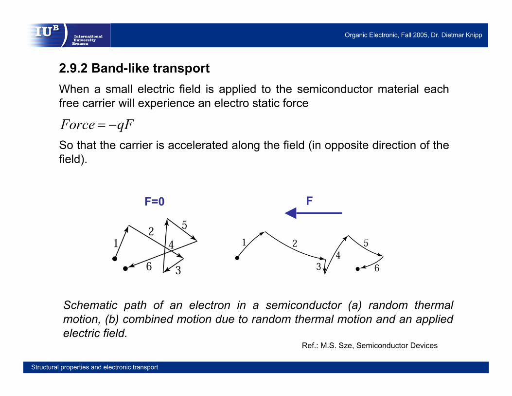
2.9.2 Band-like transportWhen a small electric field is applied to the semiconductor material each free carrier will experience an electro static force
So that the carrier is accelerated along the field (in opposite direction of the field).
Schematic path of an electron in a semiconductor (a) random thermal motion, (b) combined motion due to random thermal motion and an applied electric field.
F=0 F
qFForce −=
Ref.: M.S. Sze, Semiconductor Devices

Organic Electronic, Fall 2005, Dr. Dietmar Knipp
Structural properties and electronic transport
2.9.2 Band-like transportAn additional velocity component will be superimposed upon the thermal motion of the electron. The additional velocity is caused by an applied electric field F. The additional component is called drift velocity. The drift of the electrons can be described by a steady state motion since the gained momentum is lost due to collisions of the electrons and the lattice.
Based on momentum conservation the drift velocity can be calculated. The drift velocity is proportional to the applied electric field F.
nnvmP =
Fmqvn
Cn
τ−=
CFqP τ⋅⋅−=
Electron drift velocity

Organic Electronic, Fall 2005, Dr. Dietmar Knipp
Structural properties and electronic transport
2.9.2 Band-like transport
The mobility is an important electronic transport parameter. The mobility directly related a the material properties. Rewriting of the expression for the drift velocity leads to
The mobility is directly related to the mean free time between two collisions, which is determined by various scattering mechanisms. The most important scattering mechanisms are lattice scattering and impurity scattering. Lattice scattering is caused by thermal vibrations of the lattice atoms at any temperature above 0K. Due to the vibrations energy can be transferred from the carriers and the lattice.
n
Cn mq τµ ⋅
≡p
Vp mq τµ ⋅
≡
Fvp
p =µ
Electron and hole mobility
Fvn
n =µ Electron and hole mobility

Organic Electronic, Fall 2005, Dr. Dietmar Knipp
Structural properties and electronic transport
2.9.2 Band-like transport
Carriers can move from one molecule to the next molecule.Quantified by mobility
Mean free path > intermolecular spacing
Temperature dependent behavior:
( ) 23
−∝TTµ
Ref.: N. Karl, University Stuttgart

Organic Electronic, Fall 2005, Dr. Dietmar Knipp
Structural properties and electronic transport
20 100 30010-3
10-2
10-1
100
101
102
increasing Nt
µ tf
Temperature (K)
Mob
ility
(cm
2 /Vs)
Exponential Decrease of µEt ~ 40 - 50 meV
Dependence on Trap Density NtNt ~ 1016 - 1018 cm-3
Trap-Free Limit : Power Law T-n
n ~ 1.6 - 2.3, phonon scattering
Ref.: Dodabalapur, University Texas, lecture notes EE 396K
2.9.2 Band-like transport
Influence of traps on the electronic transport:
( ) ( )
+
=
kTE
NN
TTtraps
bulk
trapseff
exp1
0µµ

Organic Electronic, Fall 2005, Dr. Dietmar Knipp
Structural properties and electronic transport
Pentacene thin film transistor
Exp.fit
2-5µm
100-200nm
0.001
0.01
0.1
1
100 200 300 400
temperature [K]
mob
ility
[cm
2 /Vs
]
2.9.3 Grain boundaries in polycrystalline material
The mobility decreases with decreasing characterization temperature.
Temperature dependent mobility can be explained by a barrier model.
Smaller crystals leads to higher grain boundary traps density.
L
EC
EV
EF
Ei
EB
NT
−⋅=+= −−−
kTEB
GBGBGB exp011
01 µµµµµ

Organic Electronic, Fall 2005, Dr. Dietmar Knipp
Structural properties and electronic transport
2.9.4 Trap-controlled transport
µeff =µc - carrier mobility in extended states
Deep traps
Band-tail states
E = 0
Ener
gy
DOS, g(E)
Extended states
Mobility edge (E = 0)
Localized states
(Act
iva t
ion)
ene
rgy
Density-of-states distribution
Trapping and release of charges
Ref.: V. Arkhipov, IMEC

Organic Electronic, Fall 2005, Dr. Dietmar Knipp
Structural properties and electronic transport
2.9.5 Hoping transport
Jumps over-barriers dominate at higher temperatures
At lower temperatures tunneling of carriers take over
Most hopping models assume:
-positions of hopping sites are completely random
- positions and energies of hoping sites are uncorrelated E
nerg
yE
n erg
y
Ref.: V. Arkhipov, IMEC

Organic Electronic, Fall 2005, Dr. Dietmar Knipp
Structural properties and electronic transport
References
Pope and Swenburg, Electronic Processes in organic crystals and polymers, 2 ndEd., Oxford
Organic molecular crystals, E.A. Sininsh EA and V. Capek.
http://ocw.mit.edu/OcwWeb/Electrical-Engineering-and-Computer-Science/6-973Organic-OptoelectronicsSpring2003/CourseHome/
(Organic optoelectronic lecture MIT)