Embed Size (px)
Citation preview

Material Characterization
Mahendra Chaudhari
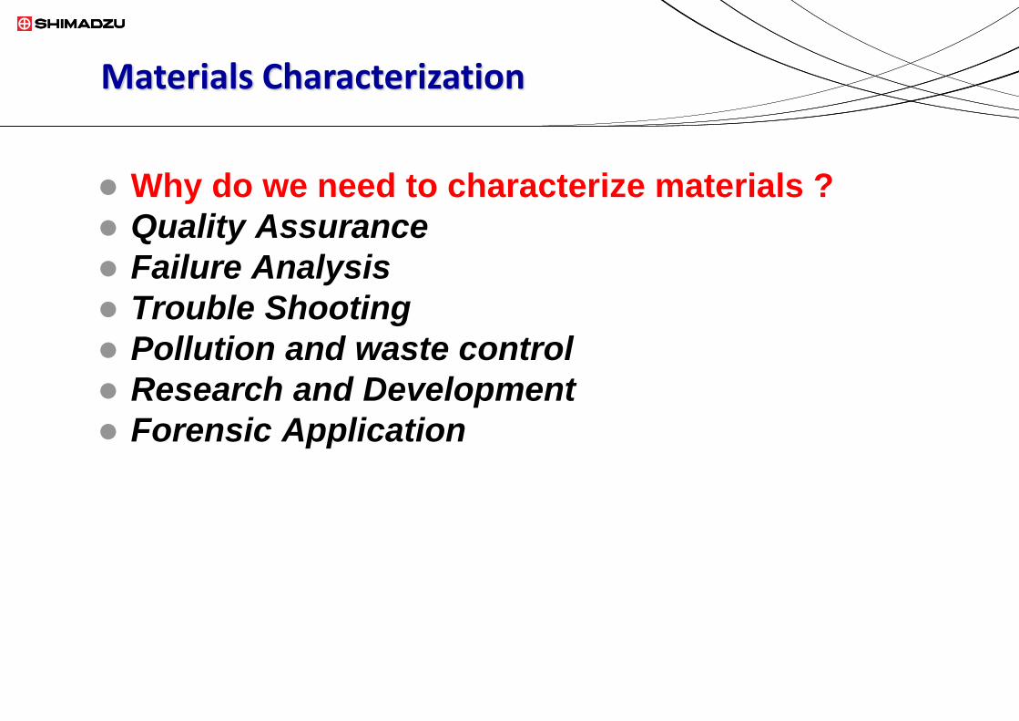
Materials Characterization
Why do we need to characterize materials ?
Quality Assurance
Failure Analysis
Trouble Shooting
Pollution and waste control
Research and Development
Forensic Application

Type of Characterization
• Physical Testing
Structural Analysis
• Elemental Analysis
• Surface Analysis
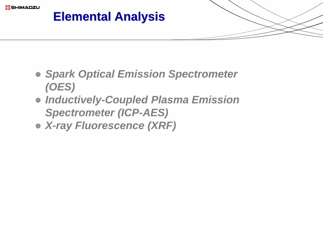
Elemental Analysis
Spark Optical Emission Spectrometer
(OES)
Inductively-Coupled Plasma Emission
Spectrometer (ICP-AES)
X-ray Fluorescence (XRF)

Optical Emission Spectrometer
Sample
Spark
PMT
detector
Grating
Ionization of sample by
electrical sparking

Optical Emission Spectrometer
PDA-5500/7000
PDA- 8000
PDA-5000 PDA-MF+

Optical Emission Spectrometer
• Vacuum Spectrometer
• High sensitive with PMT detectors
• Many options:-Fe/Al/Cu/Zn/Co/Ti bases
• From 24 to 64 elements in One minute.
• Low argon consumption
• Thermostatic control for better long
term stability.

Customized Elemental selection
ElementWavelengt
hAnalytical
Range (%)
nm Fe Cu Al Ni Co Zn Sn
C 165.8 0.005 - 0.5C 193.0 0.001 - 4.5* 0.03 - 2.5Si 212.4 0.001 - 3.5 0.01 - 7 0.05 - 2.5Si 251.6 0.001 - 5 0.001 - 1Si 390.5 1 - 30
Mn 293.3 0.001 - 2 0.0005 - 2 0.001 - 1.5 0.005 - 2 0.001 - 2 0.0005 - 0.5Mn 290.0 1 - 18 1 - 7 1 - 5P 178.3 0.001 - 0.5 0.001 - 1S 180.7 0.001 - 0.4 0.001 - 0.4
Cu 324.7 0.001 - 0.5 0.001 - 1 0.001 - 0.5 0.001 - 1 0.002 - 0.5 0.0005 - 0.1Cu 224.2 0.01 - 4 10 - 35Cu 296.1 INT.STD. 1 - 8 0.1 - 5 0.1 - 4Al 394.4 0.001 - 1.5 0.001 - 1 0.001 - 6 0.05 - 1.5 0.001 - 1 0.0002 - 0.1Al 237.2 1 - 12 INT.STD. 1 - 10Cr 267.7 0.001 - 1 0.001 - 1.5 0.001 - 0.5 0.001 - 1 0.05 - 1Cr 298.9 1 - 30 1 - 30 1 - 35
Mo 202.0 0.001 - 1 0.005 - 2 0.05 - 2Mo 277.5 0.1 - 7.5 0.1 - 30 0.1 - 10Ni 218.5 1 - 30 1 - 30 INT.STD. 1 - 3
Ni 341.4 0.003 - 1 0.001 - 1 0.001 - 2 (0.02 - 1) 0.0005 - 0.05 0.001 - 0.2
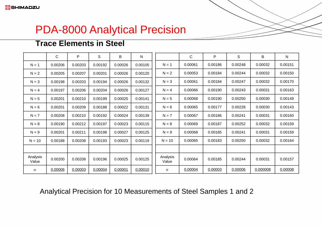
Trace Elements in Steel
C P S B N
N = 1 0.00206 0.00203 0.00192 0.00026 0.00105
N = 2 0.00205 0.00207 0.00201 0.00026 0.00120
N = 3 0.00198 0.00203 0.00194 0.00026 0.00132
N = 4 0.00197 0.00206 0.00204 0.00026 0.00127
N = 5 0.00201 0.00210 0.00199 0.00025 0.00141
N = 6 0.00201 0.00209 0.00188 0.00022 0.00131
N = 7 0.00208 0.00210 0.00192 0.00024 0.00139
N = 8 0.00190 0.00212 0.00197 0.00023 0.00115
N = 9 0.00201 0.00211 0.00198 0.00027 0.00125
N = 10 0.00188 0.00208 0.00193 0.00023 0.00119
Analysis
Value0.00200 0.00208 0.00196 0.00025 0.00125
0.00006 0.00003 0.00004 0.00001 0.00010
C P S B N
N = 1 0.00061 0.00186 0.00248 0.00032 0.00151
N = 2 0.00053 0.00184 0.00244 0.00032 0.00150
N = 3 0.00061 0.00184 0.00247 0.00032 0.00170
N = 4 0.00066 0.00190 0.00243 0.00031 0.00163
N = 5 0.00068 0.00190 0.00250 0.00030 0.00149
N = 6 0.00065 0.00177 0.00228 0.00030 0.00143
N = 7 0.00067 0.00186 0.00241 0.00031 0.00160
N = 8 0.00069 0.00187 0.00252 0.00032 0.00159
N = 9 0.00068 0.00185 0.00241 0.00031 0.00159
N = 10 0.00065 0.00183 0.00250 0.00032 0.00164
Analysis
Value0.00064 0.00185 0.00244 0.00031 0.00157
0.00004 0.00003 0.00006 0.000008 0.00008
Analytical Precision for 10 Measurements of Steel Samples 1 and 2
PDA-8000 Analytical Precision

Precision for Nickel and Chromium in Stainless Steel
Analytical Precision for 10 Measurements
C P S Ni Cr
N = 1 0.385 0.0178 0.0143 10.40 10.18
N = 2 0.384 0.0179 0.0132 10.40 10.17
N = 3 0.383 0.0177 0.0146 10.38 10.15
N=4 0.389 0.0181 0.0144 10.40 10.17
N=5 0.388 0.0183 0.0150 10.40 10.17
N=6 0.387 0.0182 0.0164 10.39 10.16
N=7 0.387 0.0184 0.0144 10.38 10.17
N=8 0.387 0.0185 0.0140 10.34 10.16
N=9 0.387 0.0183 0.0145 10.34 10.14
N=10 0.382 0.0175 0.0156 10.35 10.10
Ave. 0.386 0.0181 0.0146 10.38 10.16
0.0023 0.00034 0.00088 0.026 0.022
CV 0.59 1.88 6.01 0.25 0.22
PDA-8000 Analytical Precision
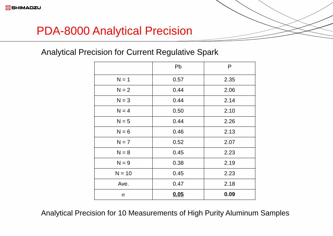
Analytical Precision for 10 Measurements of High Purity Aluminum Samples
Pb P
N = 1 0.57 2.35
N = 2 0.44 2.06
N = 3 0.44 2.14
N = 4 0.50 2.10
N = 5 0.44 2.26
N = 6 0.46 2.13
N = 7 0.52 2.07
N = 8 0.45 2.23
N = 9 0.38 2.19
N = 10 0.45 2.23
Ave. 0.47 2.18
0.05 0.09
PDA-8000 Analytical Precision
Analytical Precision for Current Regulative Spark

PDA-8000 Stability
11.60
11.70
11.80
11.90
12.00
12.10
12.20
1順目 1 3順目161 5順目321 7順目481 9順目641 11順目801 13順目961
Conte
nt
Number of Times Measured
Si in Aluminum Measured 1000 Times (SQ-15)
Seq. 3 Meas. 161Seq. 1 Meas. 1 Seq. 5 Meas. 321 Seq. 7 Meas. 481 Seq. 9 Meas. 641 Seq. 11 Meas. 801 Seq. 13 Meas. 961
0.125
0.130
0.135
0.140
0.145
0.150
0.155
11~20 111~121 211~220 311~320 411~420 511~520 611~620 711~720 811~820 911~920
Co
nte
nt
Number of Times Measured
C in Low-Alloy Steel Measured 1000 Times (SUS C)
11 to 20 111 to 121 211 to 220 311 to 320 411 to 420 511 to 520 611 to 620 711 to 720 811 to 820 911 to 920

PDA-MF series
Analysis experts on metallic materials
Product positioning
Product features
•Perfect cost-performance ratio
•Mainly concerns on enterprises of automobile and
machinery
•Linear CCD measuring system
•Double spectrometer, Air and Argon gas purge
•Digital excitation source, free from maintenance
•Unique spark stand in humanized design
•New design software, easy to use

14
PDA-MF & PDA-MF Plus
ExcitationSource
Spark stand for double spectrometer
Digital excitation source, free from maintenance
Spectrometer
Continuous spectrum measurement by linear CCD detector
Double spectrometer, Air & Argon gaspurge
Control / Power
Linear CCD measuring system
Softwear
Calibrate wavelength and intensity with one sample ( S.Cal )
Remote maintenance
New designed interface by WPF( Microsoft system )
ApplicationCalibration database with 3000 standard samples
Softwear
CCDdetector
Control / Power
Spectrometer
ExcitationSource

15
Features of PDA-MF
• Linear Multi CCD measuring system• Twin Spectrometer –Air-Argon Purge• Digital Excitation Source Unit• Plug & Play • Humanized spark stand• Best Cost to performance ratio• Alloy Judgement• Smart Intuitive software

16
Select the alloy type from analysis result.( Indicate the rate and number of agreement elements. )
Possible to find the base material even the unknown sample.
Determine by only one analysis can rapidly and automatically.( Base element judgment →Alloy judgment →Standard judgment →Result display )
Alloy Judgement
17
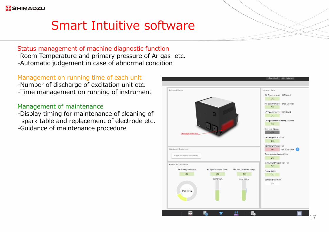
Smart Intuitive software
Status management of machine diagnostic function-Room Temperature and primary pressure of Ar gas etc.-Automatic judgement in case of abnormal condition
Management on running time of each unit-Number of discharge of excitation unit etc.-Time management on running of instrument
Management of maintenance-Display timing for maintenance of cleaning ofspark table and replacement of electrode etc.
-Guidance of maintenance procedure

18
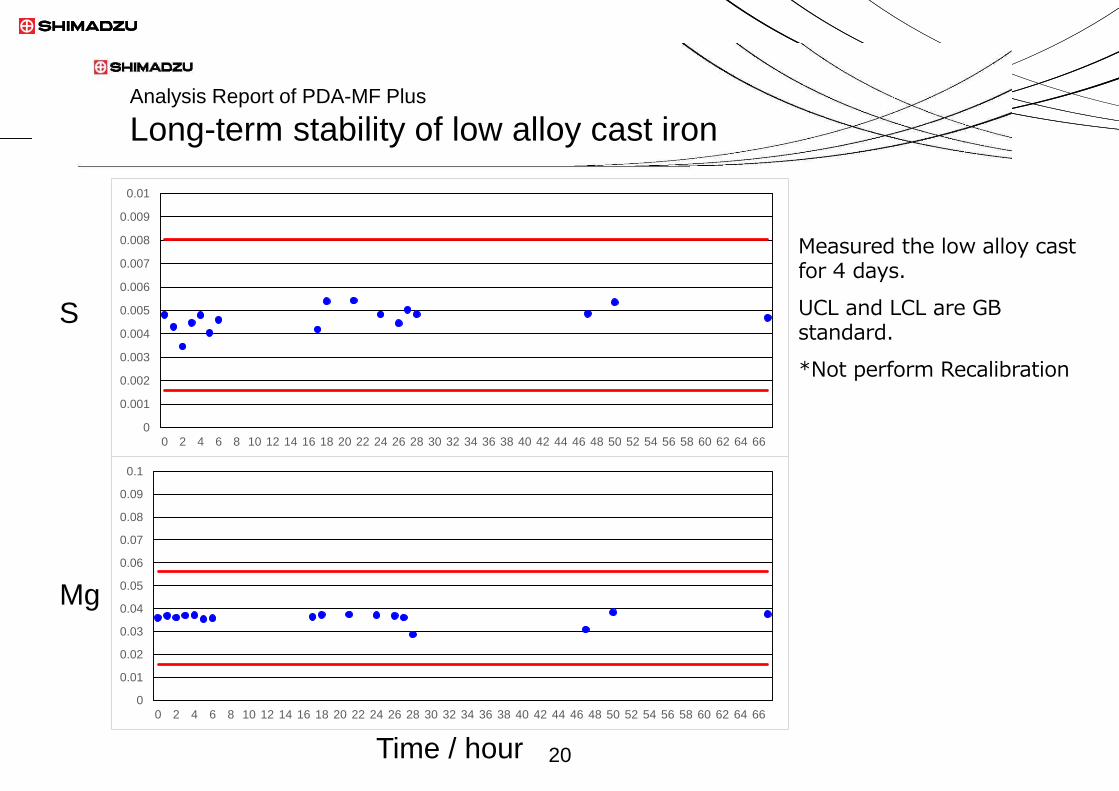
Analysis Report of PDA-MF Plus
Long-term stability of low alloy cast iron
2.5
2.6
2.7
2.8
2.9
3
3.1
3.2
3.3
3.4
3.5
3.6
3.7
3.8
0 2 4 6 8 10 12 14 16 18 20 22 24 26 28 30 32 34 36 38 40 42 44 46 48 50 52 54 56 58 60 62 64 66
0.9
0.95
1
1.05
1.1
1.15
1.2
1.25
1.3
1.35
1.4
0 2 4 6 8 10 12 14 16 18 20 22 24 26 28 30 32 34 36 38 40 42 44 46 48 50 52 54 56 58 60 62 64 66
C
Si
Time / hour
Measured the low alloy castfor 4 days.
UCL and LCL are GB standard.
*Not perform Recalibration

19
Analysis Report of PDA-MF Plus
Long-term stability of low alloy cast iron
Mn
P
Time / hour
0.8
0.85
0.9
0.95
1
1.05
1.1
1.15
1.2
1.25
1.3
0 2 4 6 8 10 12 14 16 18 20 22 24 26 28 30 32 34 36 38 40 42 44 46 48 50 52 54 56 58 60 62 64 66
0.005
0.015
0.025
0.035
0.045
0.055
0.065
0.075
0.085
0.095
0.105
0.115
0.125
0.135
0.145
0.155
0 2 4 6 8 10 12 14 16 18 20 22 24 26 28 30 32 34 36 38 40 42 44 46 48 50 52 54 56 58 60 62 64 66
Measured the low alloy castfor 4 days.
UCL and LCL are GB standard.
*Not perform Recalibration
20
Analysis Report of PDA-MF Plus
Long-term stability of low alloy cast iron
S
Mg
Time / hour
0
0.001
0.002
0.003
0.004
0.005
0.006
0.007
0.008
0.009
0.01
0 2 4 6 8 10 12 14 16 18 20 22 24 26 28 30 32 34 36 38 40 42 44 46 48 50 52 54 56 58 60 62 64 66
0
0.01
0.02
0.03
0.04
0.05
0.06
0.07
0.08
0.09
0.1
0 2 4 6 8 10 12 14 16 18 20 22 24 26 28 30 32 34 36 38 40 42 44 46 48 50 52 54 56 58 60 62 64 66
Measured the low alloy castfor 4 days.
UCL and LCL are GB standard.
*Not perform Recalibration

X-ray Fluorescence Spectrometer
Energy Dispersive Type
EDX-7000/8000
Wavelength Dispersive Type
XRF-1800
Applications: To determine the elemental information quantitatively & qualitatively
of bulk, powder or liquid samples at ppm ~ % level.

X-ray Fluorescence Spectrometer
EDX-7000/8000/8100
• Na to U/C to U
• High sensitive
• Powder/Solids/ Liq
• Vacuum/Air/He
• Sample turret
• RoHs/Halogen
Screening
• Fast analysis

Energy Dispersive Type
EDX-LE
X-ray Fluorescence Spectrometer
• Al to U
• Pin Diode detector
• Powder/Solids/ Liq
• Light & Easy
• RoHs Screening
• Halogen Screening

X-ray Fluorescence Spectrometer
Sequential Type
XRF-1800
Simultaneous Type
MXF-2400
Wavelength Dispersive Type

X-ray Fluorescence Spectrometer
Sequential Type XRF-1800 Simultaneous Type MXF-2400
Wavelength Dispersive Type
• Be to U
• CCD Optional
• 250micron analysis
• Sc & FP detector
• Powder/Solids/ Liq
• 4KW Power
• Vacuum/He
• Turret
• Be to U
• Many detectors
• Powder/Solids/ Liq
• 4KW Power
• Simultaneous+ scanner
• 1min max 36 elements
analysis

X-ray Fluorescence Spectrometer
Sequential Type
XRF-1800
Simultaneous Type
MXF-2400
Wavelength Dispersive Type
• Metals Oxides
• Ceramic/catalyst
• Electronics
• Thin Film
• Oil/Liq

Non-Destructive Analysis
X-ray analysis techniques are classified as non-destructive testing.
• Samples are generally difficult to digest into
liquid form for AAS, IPCS, ICPMS.
• Samples can be conductive or non-
conductive bulk samples.

Structural Analysis
Crystal Studies
Phase Analysis
Texture-stress analysis
Lattice strain
Lattice parameters

What is Crystal?
Crystal structure of NaCl
The crystal consists of by arranging the atoms or molecules in the
smallest 3-D structure (a parallel hexahedron). This smallest
parallelism hexahedron is called “unit cell”.
Crystal and Amorphous
CrystalIt has a structure that is regularly arranged
atoms and molecules is shown on the left in
the solid material.
AmorphousIt is a solid material that does not have a
regular arrangement of atoms and molecules.
(Example; glass)

Crystal System
Crystal Structure are classified in
seven crystal systems as follows
• Cubic• Tetragonal• Orthorhombic• Rhombohedral• Hexagonal• Monoclinic• Triclinic
It is possible to classify the crystal lattice of the 14 types (Bravais lattice) in consideration of the symmetry of the crystal.

X-ray Diffractometer
Crystal Determination
Samples can be in bulk form
(eg Steel, Stones) or powder
form (eg catalyst, geological
powder)
Applications: To determine qualitatively and
quantitatively of crystals in a compound sample.
XRD-6100/7000

XRD6100 & XRD7000
32
XRD-6100
XRD-7000
Scintillation detector1-D semiconductor detector


New Analysis Software for OneSight
34
Ribbon type interface
Window of each
condition file
Status display of XRD
main body
Status display for the
measurement
Detail information display window of
measurement condition
Windows for scheduling
Profile display window for
on going

Comparison between OneSight and SC detector
Pro
file
s b
y O
ne
Sig
ht
Scintillation detector (50 min)
High speed mode
High resolution mode
Standard mode
1/10
1/15
1/25
Measurement time
Measurement time
Only 2 min!
List price:266,000yen
List price:4,500,000Yen
OneSight
sample:Si powder
35
Measurement time

Example of Analysis (zeolite, low angle )
1/5
1/10
1/25
36
Scintillation detector (2deg/min)
High speed mode
(50deg/min)
High resolution mode
(10deg/min)
Standard mode
(20deg/min)
Pro
file
s b
y O
ne
Sig
ht
Measurement time
Measurement time
Measurement time

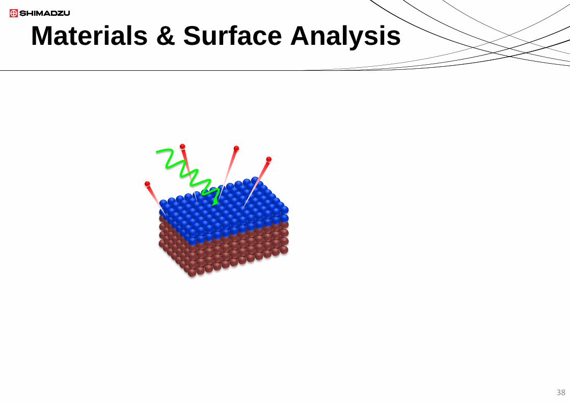
Surface Analysis
MICRO ANALYSIS
MACRO ANALYSIS
SURFACE IMAGING
TOPOGRAPHIC ANALYSIS
38
Materials & Surface Analysis

• Materials characterisation
o what elements / chemical states are present, the physical properties etc.
• QA/QC of manufacturing processes
o is the product to standard?
• Failure Analysis
o is contamination present?
• Process/product development / optimisation
o multivariate analysis – identification of key parameters
Why characterise?

Materials Analysis
Bulk vs. Surface
• Cohesion
• Density
• Morphologies
• Homogeneity
• Young’s Modulus
• Hardness
• Composition
• Surface Composition
• Surface Roughness
• Homogeneity
• Surface charge
• Adhesion

Bulk vs. Surface: Techniques
SurfaceUHVToF-SIMS(<1nm)
ATR-IR(0.2-2μm)
UHVXPS(1-12nm)
UHVAES(1-5nm)
Raman(1-5μm)
SEM-EDX(0.3-3μm)
Sub-SurfaceDepth Profiling
→Etching
Mono – sources
Cluster Ions
Bulk
FT-IR(0.5-2μm)
XRF(1-10μm)
XRD(10nm-10μm)
Atomic Scale
TEM-EDX(2-100nm)
TEM-EELS(2-100nm)
XRR (0.001-1μm)
Buried LayerAFM(0.1nm-20μm)
Interferometry(500μm)
Tensile Testing
Physical
Properties
UHVISS(top atomic layer)
STM(0.01 nm)
Surface Profile
10 nm
300 nm
900 nm

Surface Analysis: Industrial Examples
• Semi-conductors
• Bio technology
• Self assembled monolayers (SAMs)
• Thin films / coatings & adhesion
• Plasma / flame treated surfaces
Journal of Biomaterials and Nanobiotechnology, 2012, 3, 87-91
Polymer, 2010, 51, 3591-3605
GOLD
Before Flame After Flame

XPS’s place in Surface Analytics
Features/ Advantages:• Quantitative chemical analysis ~0.1 atom% detection limit• Able to detect all elements except H and He • Non-destructive analysis• Chemical state information• Depth profiling – accessing buried layers• Angle resolved – enables thin film analysis < 10nm• Imaging
Can be complimentary to:• ToF-SIMS (Quantitative vs qualitative, surface sensitivity)• XRF (Surface vs bulk)

44
The Photoelectron Process
X-rays in photoelectrons out
Sample Surface Layer
binding energy (eV) = photon energy - kinetic energy - work function
BE (eV) = hn - KE - f
fEv
Ef
KE
BEValence
band
core
levels
photon
Fermi level
Vacuum level
In vacuum final state

1200 1000 800 600 400 200 0
45
3d5/2
3d3/2
• Photoemission Peaks
• Auger Peaks
• Satellites/ shake-up
• Ghosts
• Plasmons
• Valence band structure
• Background =
inelastically scattered
photoelectrons
The Photoelectron Spectrum
Binding Energy / eV
Ag MN1
Ag 3s
Ag 3p1/2
Ag 3p3/2
Ag 3d3/2
Ag 3d5/2
Ag 4sAg 4p1/2
Ag 4p3/2
Valence
420 400 380 360 340 320Binding Energy (eV)
x104
8
16
24
32
40
x104
Inte
nsity (
cp
s)
8
16
24
32
40
Inte
nsity (
cp
s)
400 600 800 1000 1200 1400 Kinetic Energy / eV

46
What information do we get from XPS?
Surface sensitivity - photoelectron signal from first 1-10 layers of atoms and molecules.
Element identification (except H & He) at concentrations from 0.1 atomic %
Quantitative determination of the elemental composition
Chemical state information - molecular environment of the element
Non-destructive analysis, including depth profiles, from the top 10 nm (angle resolved XPS)
Destructive depth profiles of inorganic materials or organic materials (e.g. using a gas cluster source for sputtering the surface)
Imaging - lateral variations in surface composition
‘Finger printing’ of materials using valance band

Resolution & Sensitivity
• Tailor experiments for sensitivity & resolution (full width half maximum, FWHM)
47
Log
10
[Se
nsitiv
ity (
cp
s)]
FWHM
• Full width half maximum (FWHM) is a measure of resolution in
XPS = full width at half of the maximum value (i.e. half of the cps
recorded at the peak height)
• High FWHM → low resolution
• Low FWHM → high resolution
• Counts per second (cps) is the number of signals detected
• High cps → greater sensitivity
• Low cps → lower sensitivity
• Use high pass energy for low concentration elements
→ max sensitivity, but lower resolution
• Use low pass energy for chemical state information
→ lower sensitivity, but high resolution
cpsmax
½ .cps
cps
FWHM
BE1 BE2 BE

48
Chemical State Information
The binding energy of an electron is dependent on the atomic orbital the electron occupies &
the chemical environment of the atom
XPS therefore provides information on the chemical state of the atom or ionCore level electron, high binding energy
Valence electron, low binding energy
C 1s photoemission peaks from organic materials
Functional group B.E (eV)
hydrocarbon C-H, C-C 285.0
amine C-N 286.0
alcohol, ether C-O-H, C-O-C 286.5
fluorocarbon C-F 287.8
carbonyl C=O 288.0
2F bound to a carbon -CH2CF2- 290.6
3F bound to a carbon -CF3 293-294
O 1s photoemission peaks from organic materials
Functional group B.E. (eV)
carbonyl -C=O, O-C=O 532.2
alcohol, ether -O-H, O-C-O 532.8
ester C-O-C=O 533.7

• Two samples:
1. Thick film SiO2 film on Si
2. Thin film SiO2 film on Si
49
Chemical State: Si
Si oxide
Si elemental
d d
Si elemental
Si oxide
→Large chemical shift between
elemental Si & silicon dioxide peaks
1 2
108 106 104 102 100 98
Binding Energy (eV)
8
16
24
32
40
Inte
nsity (
cp
s)
x102
12

50
Quantitative Surface Analysis
Poly(ethylene terephthalate) - PET → Large Area Survey
O KLL
C 1s
O 1s
60
50
40
30
20
10
Inte
nsity (
cp
s)
1000 800 600 400 200 0
Binding Energy (eV)
x104
Peak Position B.E. (eV) Atomic Conc. (%)
C 1s 282 74.54
O 1s 530 25.46

51
Beyond Large Area Spectroscopy
Thin film
<10 nm
Thicker layer or multilayers Heterogeneous surface
Angle resolved XPS Depth profileSelected area
spectroscopySurface imaging

Angle Resolved XPS
d*
X-rays
photoelectrons
d = 3 – 10 nm
d > d*d
photoelectronsX-rays
θ
d

Depth Profiling
53
Multi-layered Structure:

Layer 1
Layer 2
Layer 1
Layer 2
Layer 1
Layer 2
Layer 1
Layer 2
Depth Profiling
54
• Depth profiling allows the identification of the chemical
nature buried beneath the surface layers
o The rate of etching depends on material properties
o Organic and inorganic materials is possible
X-raysX-raysX-raysX-rays
DetectorDetectorDetectorDetectorDetector
Ion gun
X-rays
Distance into sampleIn
tensity

Depth Profiling
55
TiN
SiO2
Si substrate
• Full chemical state concentration depth profile through TiN film:
• Can determine film thickness

Imaging
56
F 1s
• Imaging allows the identification of inhomogeneity
• 1µm lateral resolution achievable on Supra
• Stitching of images allows larger area analysis
PTFE substrate
metal mesh mask

57
3x3 stitched
3x3 stitched
parallel image
1x3 stitched
parallel image
Stitched imaging
• Stitching of images allows larger area analysis:
100 µm
Si 2p
Si 2p
300 µm
300 µm

ES-100 launched 1969
XSAM series 1980-90
Axis series launched 1990
AXIS HS 3 detectors
AXIS HSi 5 detectors
AXIS 165 8 detectors
AXIS Ultra
AXIS UltraDLD
AXIS Nova
AXIS Supra
1969
ES-100 ES-200ES-300
XSAM
series HS1984
2004
AXIS Nova
AXIS UltraDLD
2003
AXIS Ultra
1997
AXIS 165
1994
AXIS HSi
1991
Building on 45 years of XPS at Kratos
AXIS Supra
2014
Kratos Analytical launched the first
commercially available photoelectron
spectrometer in 1969 and since then has
continuously lead the field of surface
analysis with innovations such as the
magnetic immersion lens, spherical mirror
analyser for parallel imaging and more
recently the delay-line detector for imaging
and spectroscopy.

Axis Supra Axis Nova
Amicus
Kratos-XPS Lineup

Amicus
Du-pont Analyzer
Powerful with 10
sample caraosol
High Sensitivity
Cost effective
Low maintenance
Max 8mm diameter
sample
![EDX607簡單説明 - EVEREN · EDX-607A [EUM-E] 8 2 Operations 2-0 EDX System EDX is a protocol specifically designed for architectural and environmental lighting applications. EDX](https://img.pdfslide.net/doc/110x75/5f18f58ef251541adb2efb7e/edx607ce-everen-edx-607a-eum-e-8-2-operations-2-0-edx-system-edx-is.jpg)


![esp - · PDF fileesp pop edx Datum pop ecx ret add eax,[edx] push edi ret mov [edx], ecx ret pop edi ret ret pop edx ret Bachelorstudiengang Informatik/IT-Sicherheit](https://img.pdfslide.net/doc/110x75/5a9d34507f8b9a032a8c9609/esp-pop-edx-datum-pop-ecx-ret-add-eaxedx-push-edi-ret-mov-edx-ecx-ret-pop.jpg)