Embed Size (px)
Citation preview
24/04/2018
1
Introduction to Transmission Electron Microscopy
(Physical Sciences)
Centre for Advanced Microscopy
Program
9:00 – 10:15 Lecture 1 – Basics of TEM
10:15 – 10:30 Morning tea
10:30 – 11:45 Lecture 2 – Diffraction
11:45 – 12:00 Practice 1 – Indexing diffraction patterns
12:00 – 12:30 Demonstration 1 – Basics of TEM operation
12:30 – 13:30 Lunch
13:30 – 14:45 Lecture 3 - Imaging
14:45 – 15:00 Afternoon tea
15:00 – 15:30 Demonstration 2 – Collection of diffraction patterns and images
15:30 – 16:00 EDX, STEM

24/04/2018
2
• Transmission Electron Microscopy and Diffractometry of Materials. Brent Fultz and James Howe
• Transmission Electron Microscopy: A Textbook for Materials Science David B. Williams and C. Barry Carter
• Transmission Electron Microscopy: Physics of Image Formation. L. Reimer H. Kohl
• Introduction to Conventional Transmission Electron Microscopy. Marc de Graef
• Scanning Transmission Electron Microscopy: Imaging and Analysis. S. J. Penycock and P. Nellist
• Essential software: Digital micrograph, ImageJ
• Other useful software: JEMS (available in CAM), Crystal Maker, CRISP
• Contact: [email protected]
• For initial sessions and training in the TEM, please contact:
– [email protected] or [email protected]
Notes

24/04/2018
3
Part 1The basics of TEM
Centre for Advanced Microscopy
E-learning room
Introduction
24/04/2018
4
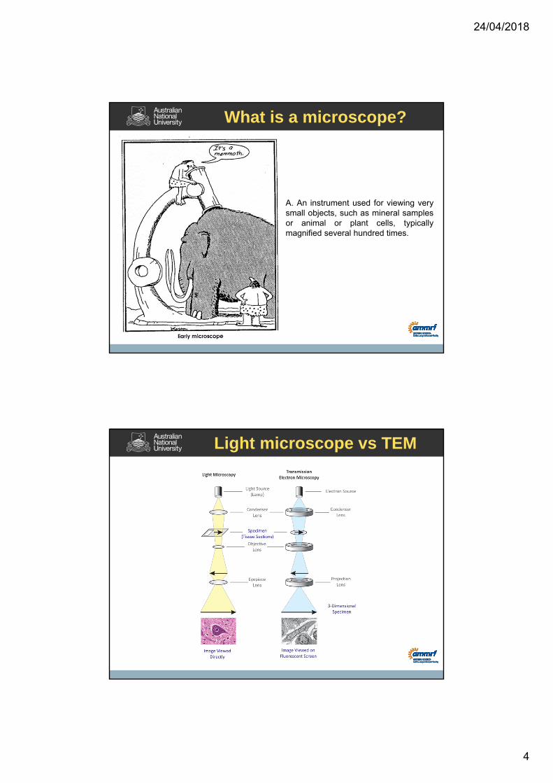
What is a microscope?
A. An instrument used for viewing verysmall objects, such as mineral samplesor animal or plant cells, typicallymagnified several hundred times.
Light microscope vs TEM

24/04/2018
5
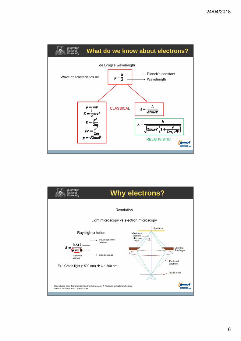
What do we know about electrons?
What do we know about electrons:
Amber = elektron ()
Negatively charged particles => We can apply an electric field to accelerate it!
Electron Duality
Behave as waves => Diffraction patterns when passing by crystals
Behave as particles => Excitation of inner shell electrons => x-ray chemical analysis
What do we know about electrons?
Electron DualityWave characteristics of the electron gives rise to coherent scattering (diffraction)
Particle characteristics gives rise to characteristic X-rays
Reproduced from: Transmission Electron Microscopy: A Textbook for Materials ScienceDavid B. Williams and C. Barry Carter
24/04/2018
6
What do we know about electrons?
de Broglie wavelength
Wave characteristics =>
CLASSICAL
RELATIVISTIC
Planck’s constant
Wavelength
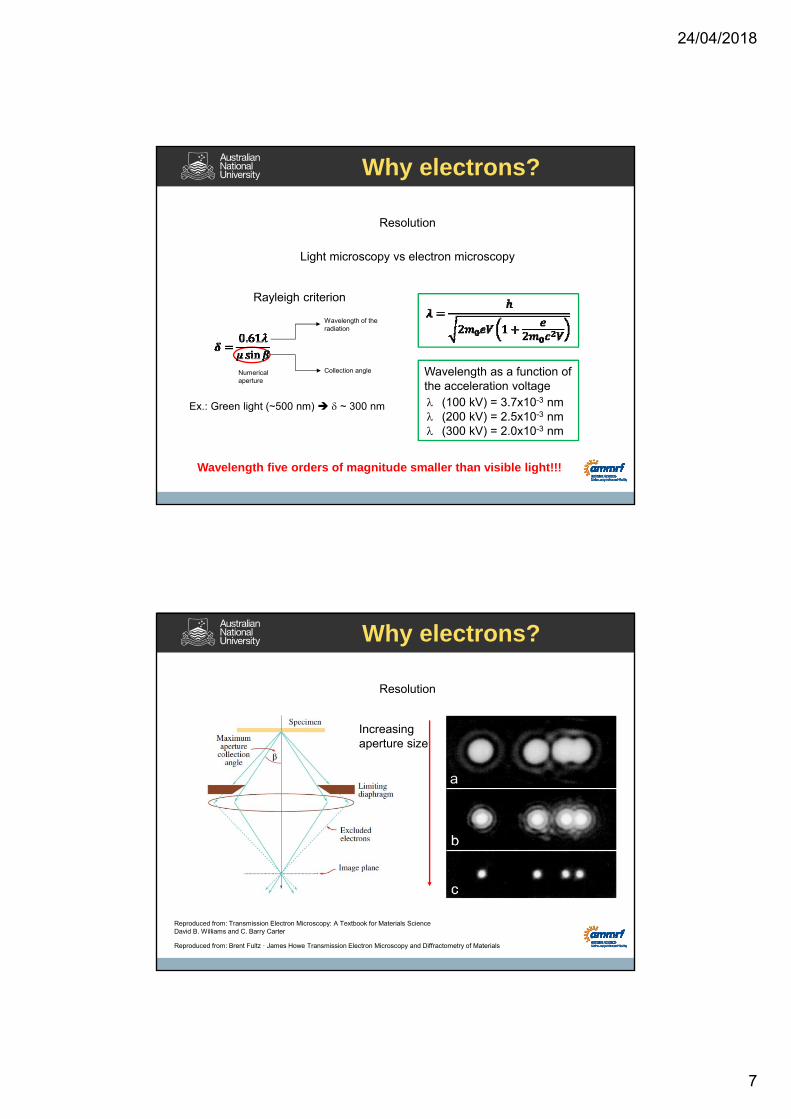
Why electrons?
Resolution
Light microscopy vs electron microscopy
Wavelength of the radiation
Collection angleNumerical aperture
Rayleigh criterion
Reproduced from: Transmission Electron Microscopy: A Textbook for Materials ScienceDavid B. Williams and C. Barry Carter
Ex.: Green light (~500 nm) ~ 300 nm
24/04/2018
7
Why electrons?
Wavelength of the radiation
Collection angleNumerical aperture
Rayleigh criterion
Ex.: Green light (~500 nm) ~ 300 nm (100 kV) = 3.7x10⁻³ nm (200 kV) = 2.5x10⁻³ nm (300 kV) = 2.0x10⁻³ nm
Resolution
Light microscopy vs electron microscopy
Wavelength as a function of the acceleration voltage
Wavelength five orders of magnitude smaller than visible light!!!
Reproduced from: Brent Fultz · James Howe Transmission Electron Microscopy and Diffractometry of Materials
Why electrons?
Resolution
Reproduced from: Transmission Electron Microscopy: A Textbook for Materials ScienceDavid B. Williams and C. Barry Carter
Increasing aperture size

24/04/2018
8
Resolution vs Magnification
A B C
“A” has same Mag than “C”“B” has same Res than “C”
d
D
Mag = D/d
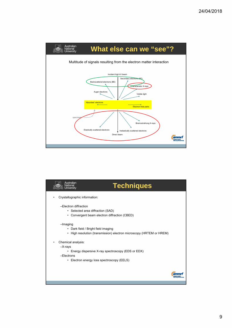
What else can we “see”?
Incident high kV beam
Secondary electrons (SE)
Characteristic X-rays
Visible light
Electron-hole pairs
‘Absorbed’ electrons
Backscattered electrons (BE)
Auger electrons
Elastically scattered electrons
Direct beam
Inelastically scattered electrons
Bremsstrahlung X-rays
specimen
Multitude of signals resulting from the electron matter interaction
24/04/2018
9
What else can we “see”?
Incident high kV beam
Secondary electrons (SE)
Characteristic X-rays
Visible light
Electron-hole pairs
‘Absorbed’ electrons
Backscattered electrons (BE)
Auger electrons
Elastically scattered electrons
Direct beam
Inelastically scattered electrons
Bremsstrahlung X-rays
specimen
Multitude of signals resulting from the electron matter interaction
Techniques
• Crystallographic information:
–Electron diffraction
• Selected area diffraction (SAD)
• Convergent beam electron diffraction (CBED)
–Imaging
• Dark field / Bright field imaging
• High resolution (transmission) electron microscopy (HRTEM or HREM)
• Chemical analysis:
–X-rays
• Energy dispersive X-ray spectroscopy (EDS or EDX)
–Electrons
• Electron energy loss spectroscopy (EELS)
24/04/2018
10
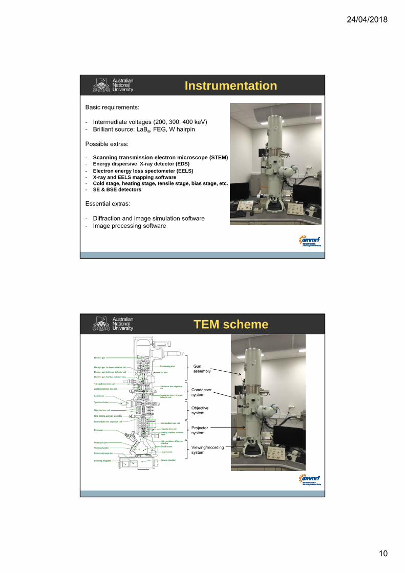
Instrumentation
Basic requirements:
- Intermediate voltages (200, 300, 400 keV)- Brilliant source: LaB6, FEG, W hairpin
Possible extras:
- Scanning transmission electron microscope (STEM)- Energy dispersive X-ray detector (EDS)- Electron energy loss spectometer (EELS)- X-ray and EELS mapping software- Cold stage, heating stage, tensile stage, bias stage, etc.- SE & BSE detectors
Essential extras:
- Diffraction and image simulation software- Image processing software
TEM scheme
Gun assembly
Condenser system
Objective system
Projector system
Viewing/recording system

24/04/2018
11
TEM scheme
Gun assembly
Condenser system
Objective system
Projector system
Viewing/recording system
Illumination
Image formation
Magnification
Jeol 2100F
TEM instrument
Gun chamber
High voltage cable
Goniometer
Viewing chamber
Condenser aperture
Left side control panel
Cold trap
Right side control panel
Objective aperture
Selected area aperture
FEI CM300
24/04/2018
12
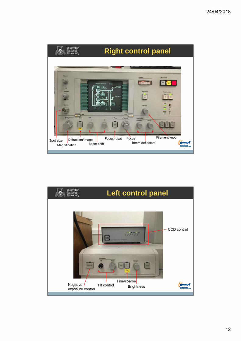
Right control panel
Spot size
Magnification
Diffraction/ImageBeam shift
Focus reset FocusBeam deflectors
Filament knob
Left control panel
CCD control
Tilt controlFine/coarse
BrightnessNegative exposure control

24/04/2018
13
Electron guns
Diameter do
Emission current icDivergence semi-angle 0
Brightness
Temporal coherence
Spatial coherence
Reproduced from: Transmission Electron Microscopy: A Textbook for Materials ScienceDavid B. Williams and C. Barry Carter
Electron guns
Thermionic emission
Diameter do
Emission current icDivergence semi-angle 0
LaB6 crystal
Reproduced from: Transmission Electron Microscopy: A Textbook for Materials ScienceDavid B. Williams and C. Barry Carter

24/04/2018
14
Electron guns
Thermionic emission
Diameter do
Emission current icDivergence semi-angle 0Transmission Electron Microscopy: A Textbook for Materials Science
David B. Williams and C. Barry Carter
Electron guns
Cold FEG (W tip)
Transmission Electron Microscopy: A Textbook for Materials ScienceDavid B. Williams and C. Barry Carter
Reproduced: Transmission Electron Microscopy: Physics of Image FormationL. Reimer H. Kohl

24/04/2018
15
Electron guns
Reproduced from: Transmission Electron Microscopy: A Textbook for Materials ScienceDavid B. Williams and C. Barry Carter
Lenses

24/04/2018
16
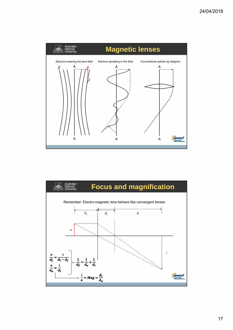
Magnetic lenses
Electro-magnetic lenses
Reproduced from: Brent Fultz · James Howe Transmission Electron Microscopy and Diffractometry of Materials
Reproduced from: Transmission Electron Microscopy: A Textbook for Materials ScienceDavid B. Williams and C. Barry Carter
Magnetic lenses
Brent Fultz · James Howe Transmission Electron Microscopy and Diffractometry of Materials
Lorentz force
Cylindrical coordinates
Convergent lens that produces a rotation to the image.
24/04/2018
17
Magnetic lenses
e-
A
A
A
A
A
A
Electron entering the lens field Electron spiralling in the field Conventional optical ray diagram
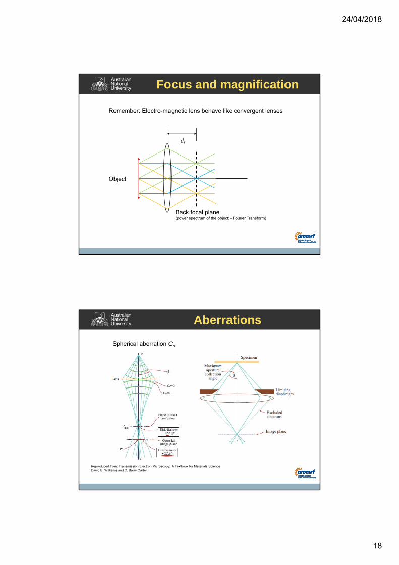
Focus and magnification
Remember: Electro-magnetic lens behave like convergent lenses
do df di
o
i
24/04/2018
18
Focus and magnification
Remember: Electro-magnetic lens behave like convergent lenses
df
Object
Back focal plane(power spectrum of the object – Fourier Transform)
Aberrations
Spherical aberration Cs
Reproduced from: Transmission Electron Microscopy: A Textbook for Materials ScienceDavid B. Williams and C. Barry Carter

24/04/2018
19
Aberrations
Spherical aberration Cs Chromatic aberration Cc
Reproduced from: Transmission Electron Microscopy: A Textbook for Materials ScienceDavid B. Williams and C. Barry Carter
#1 Condenser lens system
24/04/2018
20
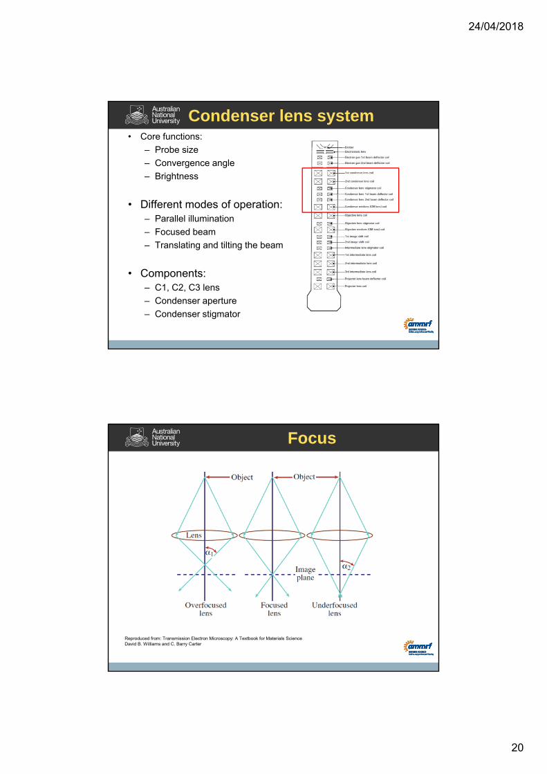
Condenser lens system• Core functions:
– Probe size
– Convergence angle
– Brightness
• Different modes of operation:– Parallel illumination
– Focused beam
– Translating and tilting the beam
• Components:– C1, C2, C3 lens
– Condenser aperture
– Condenser stigmator
Focus
Reproduced from: Transmission Electron Microscopy: A Textbook for Materials ScienceDavid B. Williams and C. Barry Carter

24/04/2018
21
C1 role (spot size)
Reproduced from: Transmission Electron Microscopy: A Textbook for Materials ScienceDavid B. Williams and C. Barry Carter
<1
Demagnification of the source
C2 role (brightness)
Reproduced from: Transmission Electron Microscopy: A Textbook for Materials ScienceDavid B. Williams and C. Barry Carter
CO or c/oCondenser-objective system
24/04/2018
22
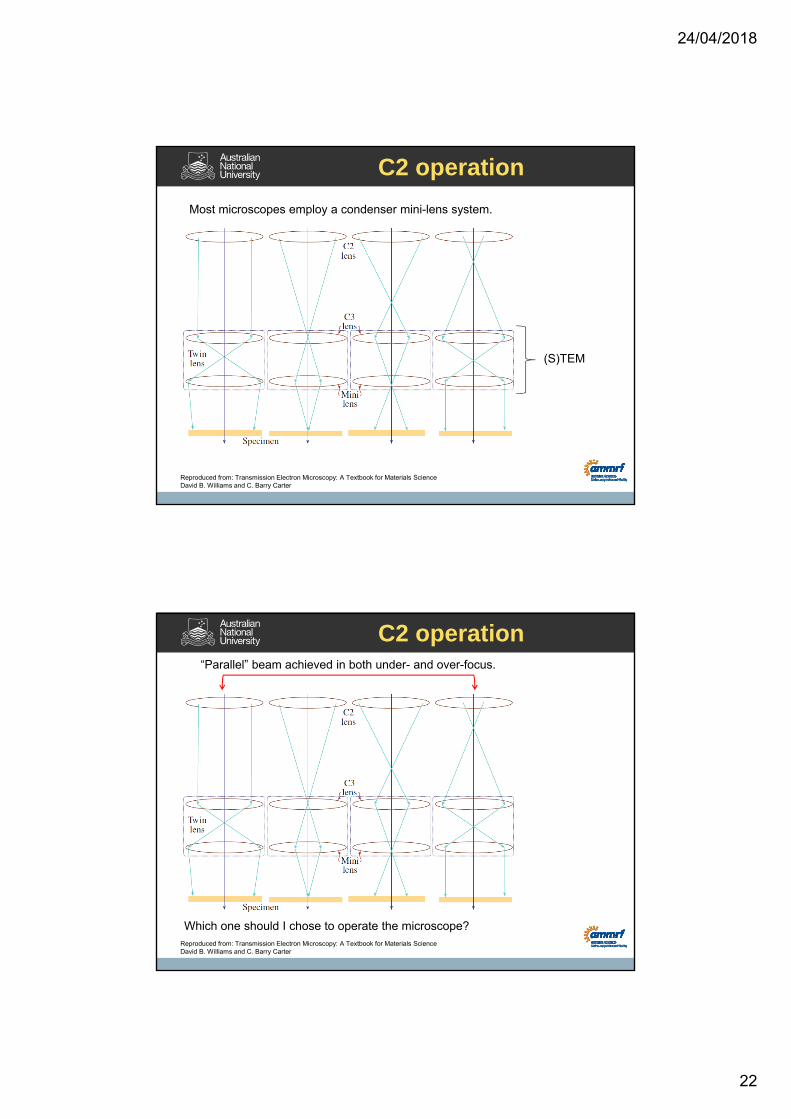
C2 operation
Reproduced from: Transmission Electron Microscopy: A Textbook for Materials ScienceDavid B. Williams and C. Barry Carter
Most microscopes employ a condenser mini-lens system.
(S)TEM
C2 operation
Reproduced from: Transmission Electron Microscopy: A Textbook for Materials ScienceDavid B. Williams and C. Barry Carter
“Parallel” beam achieved in both under- and over-focus.
Which one should I chose to operate the microscope?
24/04/2018
23
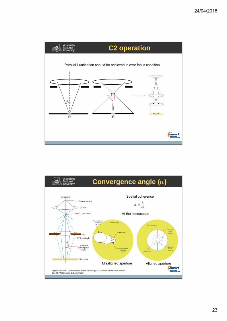
C2 operation
R
R
Parallel illumination should be achieved in over focus condition
Convergence angle ()
Reproduced from: Transmission Electron Microscopy: A Textbook for Materials ScienceDavid B. Williams and C. Barry Carter
Spatial coherence
Misaligned aperture Aligned aperture
At the microscope
24/04/2018
24
Scanning coils
y
x
Reproduced from: Transmission Electron Microscopy: A Textbook for Materials ScienceDavid B. Williams and C. Barry Carter
Reproduced from: Transmission Electron Microscopy: A Textbook for Materials ScienceDavid B. Williams and C. Barry Carter
Condenser astigmatism
Perfect lenses Real lenses Small compensating field
Result
At the microscope
Focusing the beam (C2)results in a elliptical view ofthe source. Astigmatismpresent.
Reproduced from: Transmission Electron Microscopy: A Textbook for Materials ScienceDavid B. Williams and C. Barry Carter

24/04/2018
25
More on astigmatism
The difference in the focus point between the two axis leads to the ellipsoidal shape of the electron beam.
#2 Post-specimen lenses

24/04/2018
26
Eucentric height• Z position corresponding to the
eucentric plane (reference plane towhich the calibrations arereproducible). Hence the sampleshould be kept at this height for bestperformance.
– (Eucentric plane is perpendicular tothe optic axis).
• Sample does not move laterally whentilted.
• Best position for analysis.
• At this position if the objective is infocus, then the objective-lens current isat a standard value. Therefore it ispossible to use the same lens-currentvalue independent of sample.
– It is the object plane.
Object plane
Change strength of
objective lens
Change the height z of the
sample
Eucentric height
1) Adjust the eucentric current using “standard focus”.
2) Adjust the right of the sample until minimum contrast is achieved.
Object plane
Change strength of
objective lens
Change the height z of the
sample
“standard focus”
24/04/2018
27
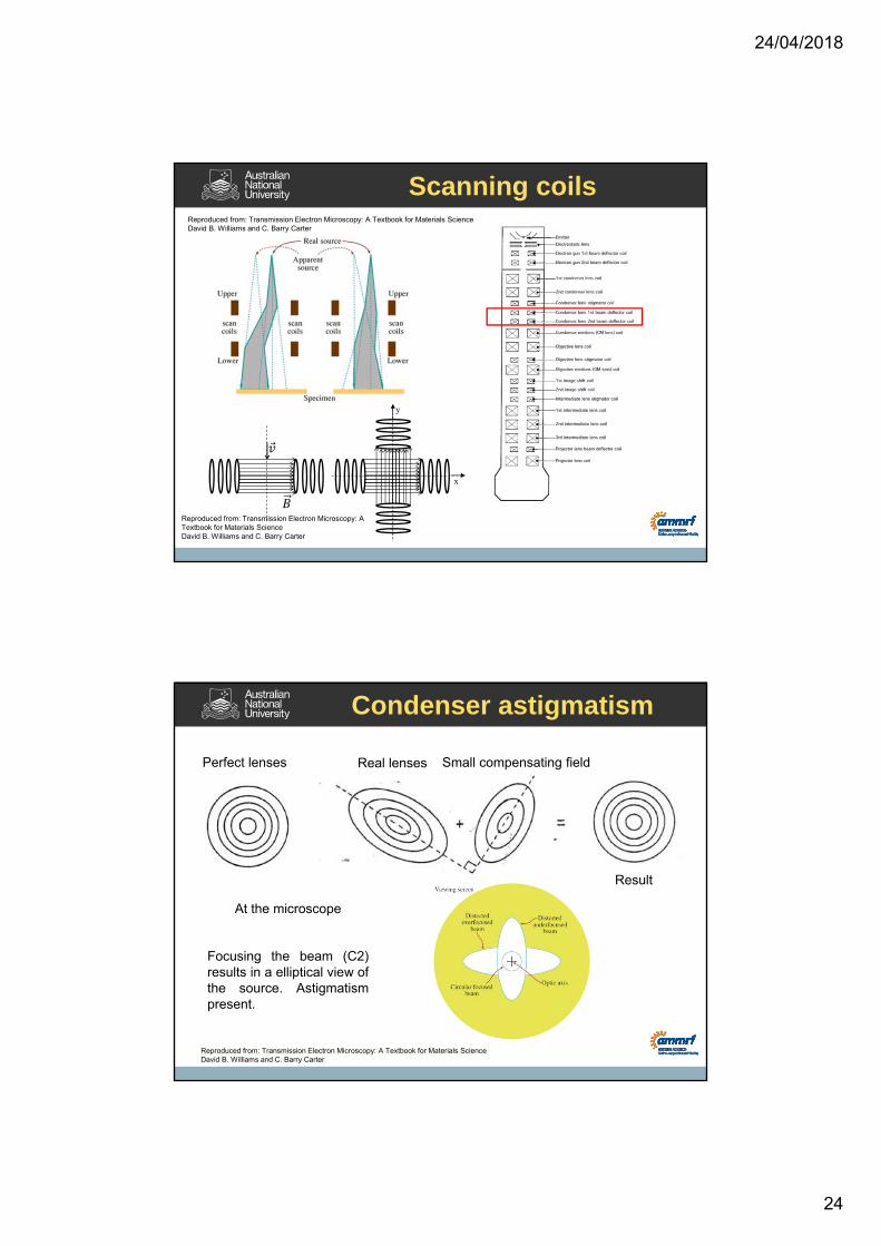
Diffraction and image modes
Image mode
Back focal plane
Objective aperture
Selected area diffraction aperture (SAD)
Intermediate lens
Projector lens
Image
Object
Objective lens
From diffraction to image mode: change in the strength of the intermediate lens

24/04/2018
28
Diffraction mode
Back focal plane
Objective aperture
Selected area diffraction aperture (SAD)
Intermediate lens
Projector lens
DP
Object
Objective lens
Diffraction mode
Intermediate lens
Projector lens
Objective lens
Diff
ract
ion
patte
rn
L = 880 mm
L = 245 mm
L = 420 mm
CM 300

24/04/2018
29
Diffraction mode
Intermediate lens
Projector lens
Objective lens
Diff
ract
ion
patte
rn
Hitachi H7100
Image mode
Intermediate lens
Projector lens
Objective lens
Imag
es
SiSiO2
Si
M = 5900x
M = 115kx M = 195kx
24/04/2018
30
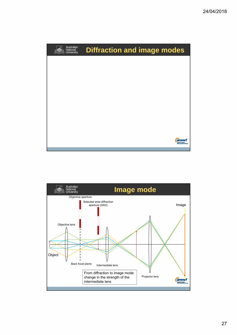
Bright and Dark field
Reproduced from: Transmission Electron Microscopy: A Textbook for Materials ScienceDavid B. Williams and C. Barry Carter
Bright Field “Dirty” Dark Field Centred Dark Field
Bright field
Reproduced from: Brent Fultz · James Howe Transmission Electron Microscopy and Diffractometry of Materials
24/04/2018
31
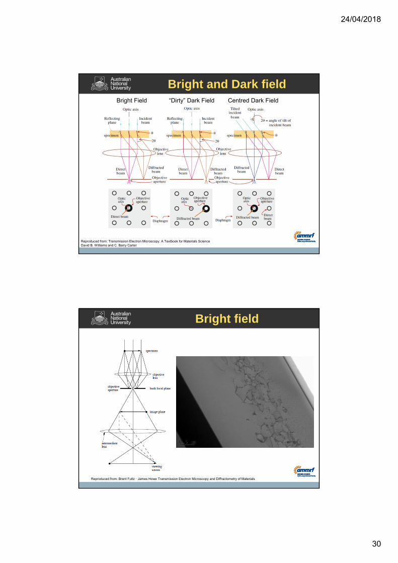
“Dirt” dark field
Reproduced from: Brent Fultz · James Howe Transmission Electron Microscopy and Diffractometry of Materials
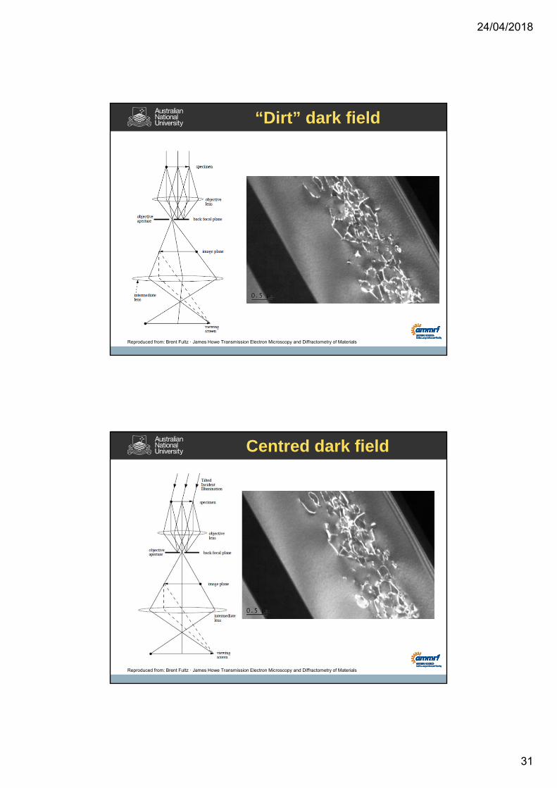
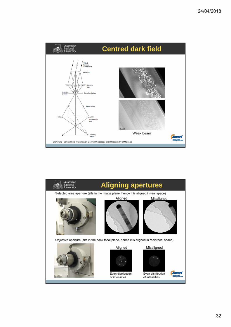
Centred dark field
Reproduced from: Brent Fultz · James Howe Transmission Electron Microscopy and Diffractometry of Materials
24/04/2018
32
Centred dark field
Brent Fultz · James Howe Transmission Electron Microscopy and Diffractometry of Materials
Weak beam
Aligning aperturesSelected area aperture (sits in the image plane, hence it is aligned in real space)
Aligned Misaligned
Objective aperture (sits in the back focal plane, hence it is aligned in reciprocal space)
Aligned Misaligned
Even distribution of intensities
Even distribution of intensities

24/04/2018
33
Optics in TEM
• TEM is primarily a scattering technique
– In materials with long range order this mean that diffraction patterns will be generated.
• The main steps in a TEM experiment are:
– Locate the region of interest
– Adjust the eucentric height
– Isolate the feature of interest with the SAD aperture.
– Switch to diffraction mode.
– Tilt the sample.
– Select which diffracted beams will contribute to the image formation.
– Back to image mode.
Reproduced from: Transmission Electron Microscopy: A Textbook for Materials ScienceDavid B. Williams and C. Barry Carter
Summary
• Electron scattering as a imaging tool
• Electron sources
• The TEM construction
• Basic TEM operation
• Lenses– Pre-specimen
• Condenser system control of electron beam illumination on the sample
– Post-specimen• Intermediate lenses Image / Diffraction modes
• Projector lenses Magnification
• Image / Diffraction mode
• Bright field imaging
• “Dirt” and Centred dark field modes

24/04/2018
34
Part 2Diffraction
Centre for Advanced Microscopy
E-learning room
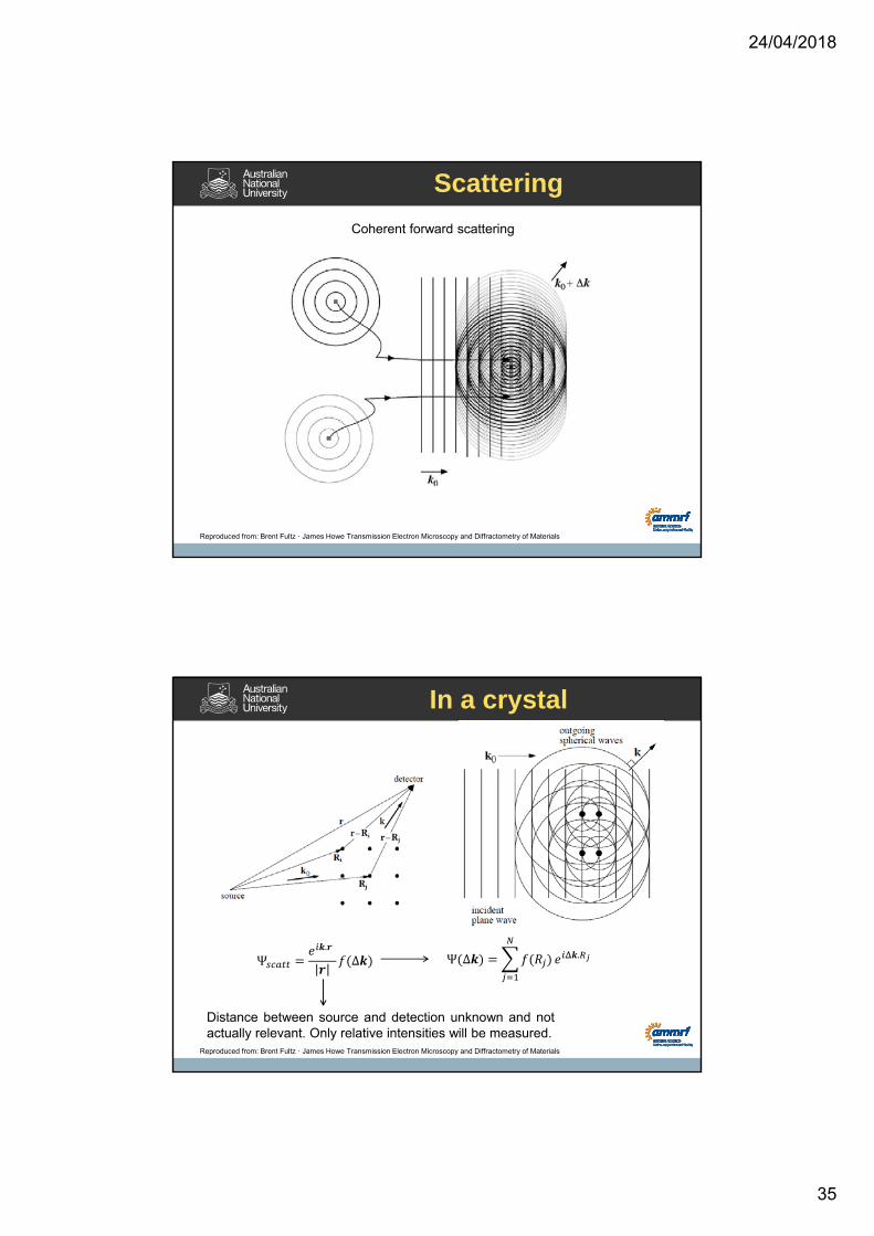
Scattering
Ψ .
Ψ.
Δ
Reproduced from: Brent Fultz · James Howe Transmission Electron Microscopy and Diffractometry of Materials
First Born approximation
Scattering center
Δ2
. ′
Scattering factor is the Fourier Transform of the scattering potential.
24/04/2018
35
Scattering
Reproduced from: Brent Fultz · James Howe Transmission Electron Microscopy and Diffractometry of Materials
Coherent forward scattering
In a crystal
Ψ.
Δ Ψ Δ .
Distance between source and detection unknown and notactually relevant. Only relative intensities will be measured.
Reproduced from: Brent Fultz · James Howe Transmission Electron Microscopy and Diffractometry of Materials
24/04/2018
36
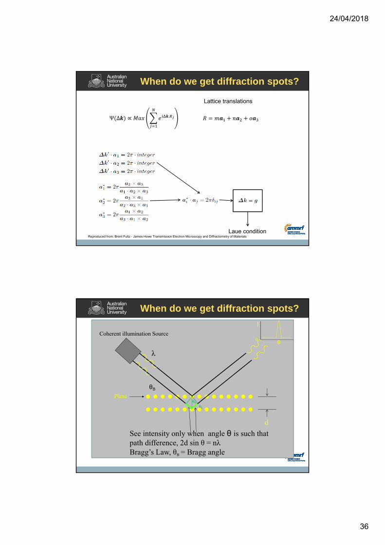
When do we get diffraction spots?
Ψ Δ ∝ .
Lattice translations
Reproduced from: Brent Fultz · James Howe Transmission Electron Microscopy and Diffractometry of MaterialsLaue condition
When do we get diffraction spots?
Plane
θB
d
Coherent illumination Source
See intensity only when angle θ is such thatpath difference, 2d sin θ = nλBragg’s Law, θB = Bragg angle
λ
θ
I
0
θBθB
24/04/2018
37
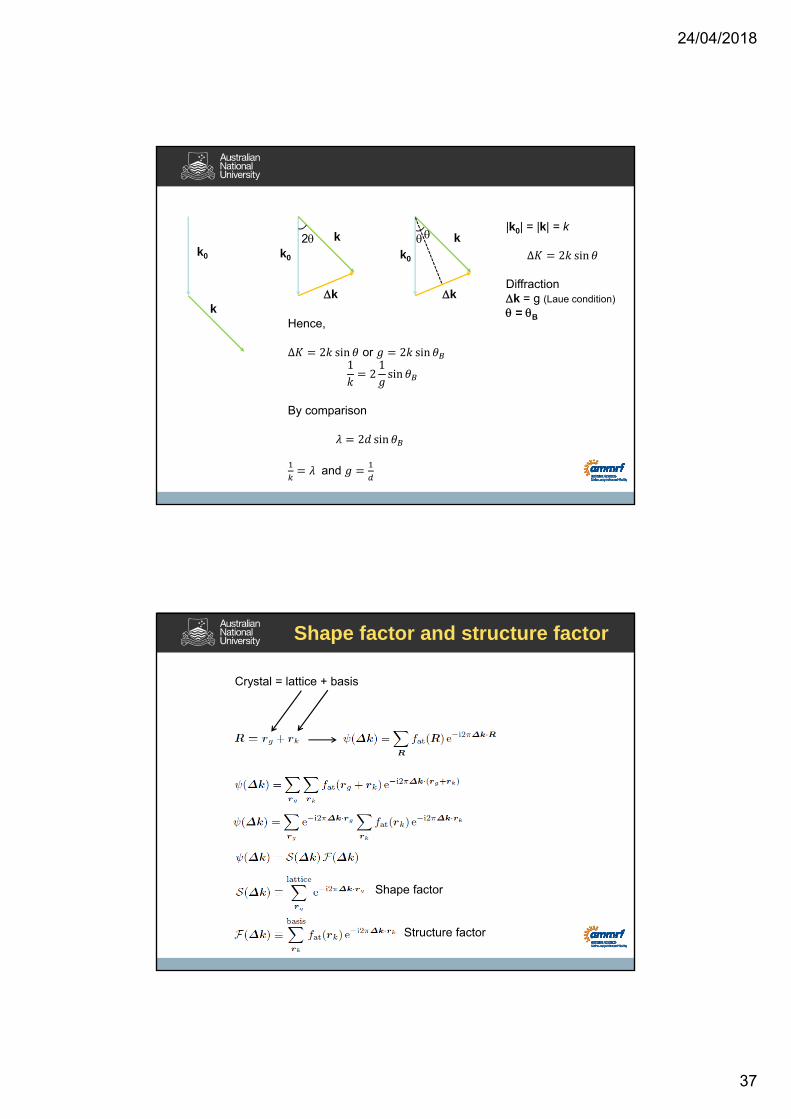
k0
k
k0
k
k0
k
k k
|k0| = |k| = k
∆ 2 sin
Diffractionk = g (Laue condition)
= B
2
Hence,
∆ 2 sin or 2 sin1
21sin
By comparison
2 sin
and
Shape factor and structure factor
Shape factor
Structure factor
Crystal = lattice + basis
24/04/2018
38
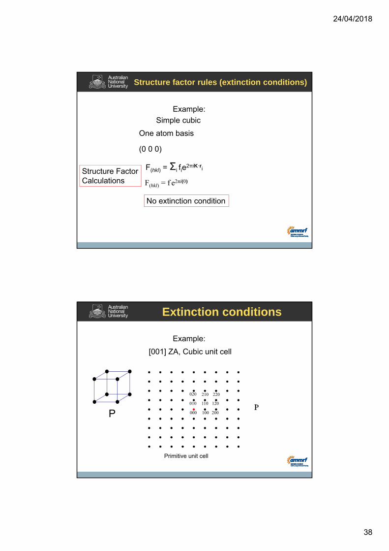
Structure factor rules (extinction conditions)
Example:
Simple cubic
One atom basis
(0 0 0)
F(hkl) = Σi fie2πiK·ri
F(hkl) = f e2πi(0)
Structure FactorCalculations
No extinction condition
Extinction conditions
Example:
000 100
010 110P
020
200
220
I
[001] ZA, Cubic unit cell
P
210
120
Primitive unit cell

24/04/2018
39
Structure factor rules (extinction conditions)
Example:
Body centred cubic
Two lattice points per unit cell
(0 0 0) and ( ½ ½ ½)
F(hkl) = Σi fie2πiK·ri
F(hkl) = f e2πi(0) + f e2πi( ½ h + ½ k + ½ l)
F(hkl) = f (1 + eπi( h + k + l) )
F(hkl) = 0 when h + k + l is odd
F(hkl) = 2f when h + k+ l is even
(N.B: eiθ = cos θ + i sin θ)
Structure FactorCalculations
Extinction conditions
I
Example:
000
110
020
200
220
[001] ZA, Cubic unit cell
I
Body centred unit cell
24/04/2018
40
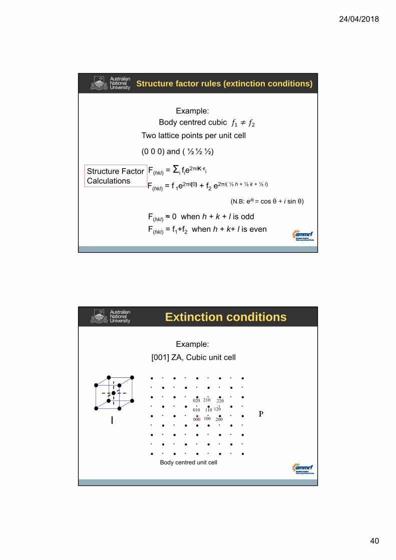
Structure factor rules (extinction conditions)
Example:
Body centred cubic
Two lattice points per unit cell
(0 0 0) and ( ½ ½ ½)
F(hkl) = Σi fie2πiK·ri
F(hkl) = f 1e2πi(0) + f2 e2πi( ½ h + ½ k + ½ l)
F(hkl) ≈ 0 when h + k + l is odd
F(hkl) = f1+f2 when h + k+ l is even
(N.B: eiθ = cos θ + i sin θ)
Structure FactorCalculations
Extinction conditions
Example:
000 100
010 110P
020
200
220
I
[001] ZA, Cubic unit cell
210
120
I
Body centred unit cell

24/04/2018
41
Extinction conditions
http://www.seas.upenn.edu/~chem101/sschem/solidstatechem.html
Lets look at the shape factor
Rectangular prism
Lets focus in the x direction

24/04/2018
42
Lets focus in the x direction 1 + + + +⋯ + Geometric series
Ψ∗Ψ ΨIntensity is the square product of the amplitude
Diffraction peaks broadened by the shape factor
Reproduced from: Brent Fultz · James Howe Transmission Electron Microscopy and Diffractometry of Materials
Lets look at the shape factor
Diffraction peaks broadened by the shape factor
Reproduced from: Brent Fultz · James Howe Transmission Electron Microscopy and Diffractometry of Materials
Nx = 12Ny = 6

24/04/2018
43
Lets look at the shape factor
Reproduced from: Brent Fultz · James Howe Transmission Electron Microscopy and Diffractometry of Materials
Crystal real shape
Diffraction intensities
Other shape factors
Simple cubic (large crystal)
Simple cubic (thin disc)
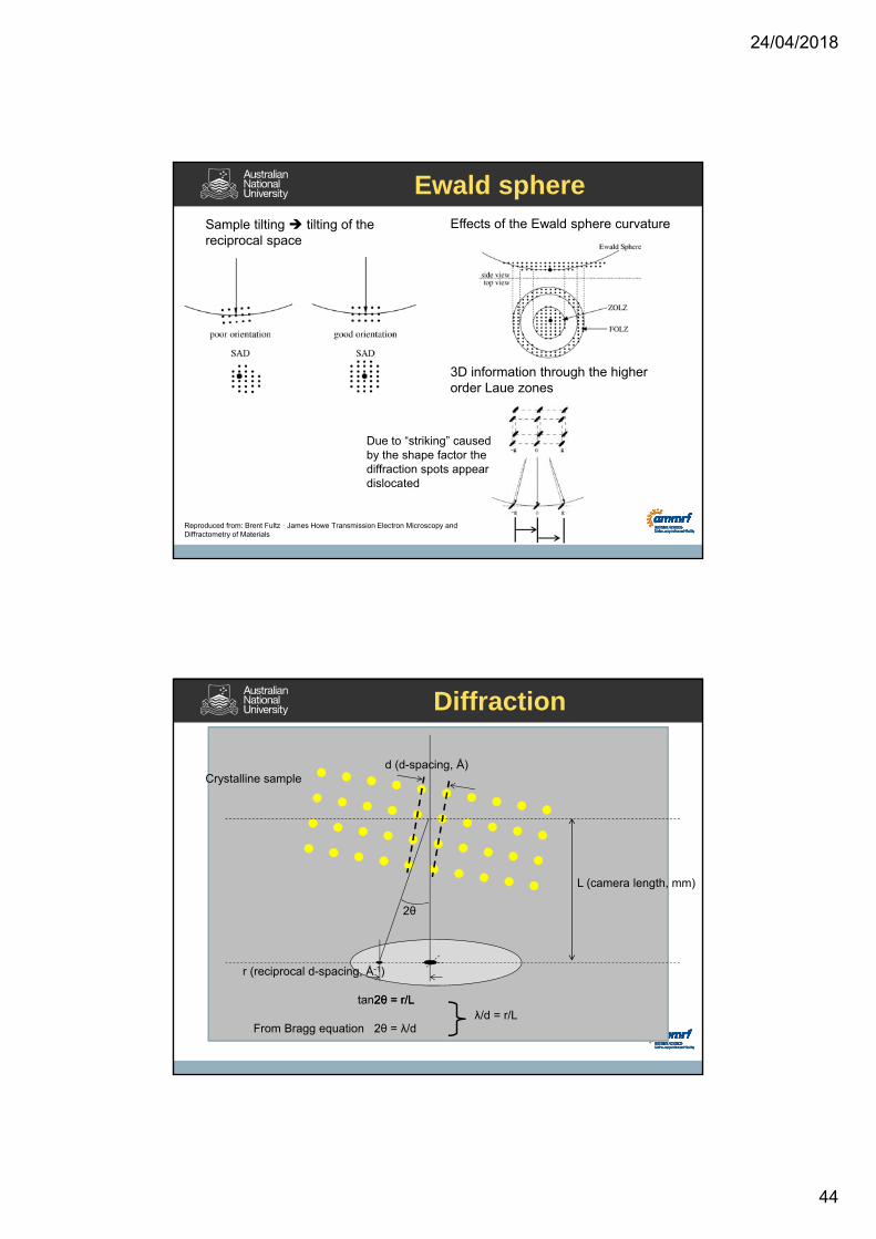
Ewald sphere
Laue condition
Diffraction occurs whenever the Ewald sphere touches a point in the reciprocal space.
The origin of the Ewaldsphere lies at the base ofthe undiffracted beam k0
Reproduced from: Brent Fultz · James Howe Transmission Electron Microscopy and Diffractometry of Materials
24/04/2018
44
Ewald sphereSample tilting tilting of the reciprocal space
Effects of the Ewald sphere curvature
3D information through the higher order Laue zones
Due to “striking” caused by the shape factor the diffraction spots appear dislocated
Reproduced from: Brent Fultz · James Howe Transmission Electron Microscopy and Diffractometry of Materials
λ/d = r/L
Crystalline sample
L (camera length, mm)
d (d-spacing, Å)
2θ
r (reciprocal d-spacing, Å-1)
tan2θ = r/L2θ = r/L
From Bragg equation 2θ = λ/d
Diffraction
24/04/2018
45
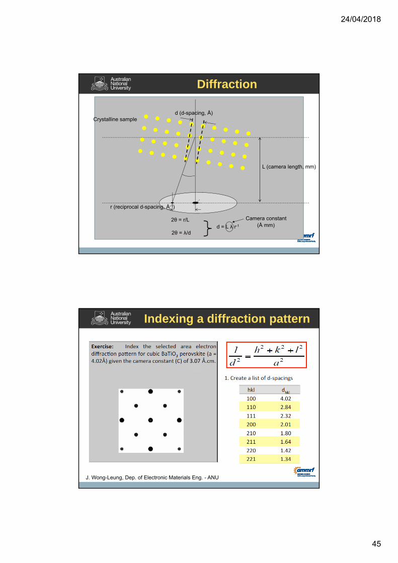
d = L λ r-1
Crystalline sample
L (camera length, mm)
d (d-spacing, Å)
2θ = r/L
2θ = λ/d
Camera constant(Å mm)
r (reciprocal d-spacing, Å-1)
Diffraction
Indexing a diffraction pattern
J. Wong-Leung, Dep. of Electronic Materials Eng. - ANU
3.07
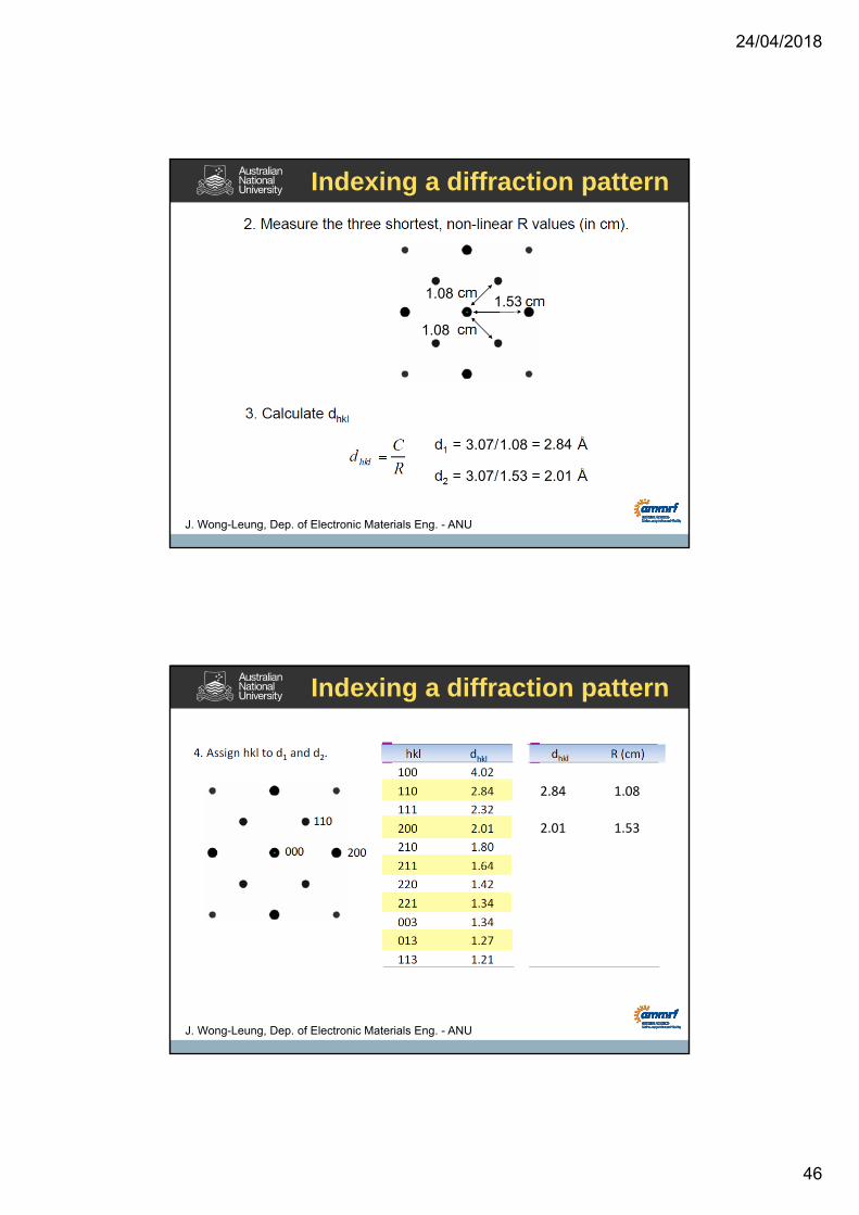
24/04/2018
46
Indexing a diffraction pattern
J. Wong-Leung, Dep. of Electronic Materials Eng. - ANU
1.08
1.08
1.53
1.083.07
1.533.07
2.84
2.01
Indexing a diffraction pattern
J. Wong-Leung, Dep. of Electronic Materials Eng. - ANU
1.08
1.53
2.84
2.01

24/04/2018
47
Indexing a diffraction pattern
J. Wong-Leung, Dep. of Electronic Materials Eng. - ANU
The diffraction pattern cannot beuniquely defined due to its symmetry.
Once a set of reflections indexed theothers must be indexed consistently.
To find the zone-axis two approachesare possible since this vector isperpendicular to the ones in this plane
#1 Dot product = 0
#2 Cross product.
Powder diffraction (polycrystalline materials)
In implanted Si0.1Ge0.9 implanted region polycrystalline
Unimplanted regions remain single crystal Ruixing (Andy) Feng - EME

24/04/2018
48
Powder diffraction (polycrystalline materials)
Reproduced: Transmission Electron Microscopy: Physics of Image FormationL. Reimer H. Kohl
Summary
• Diffraction is a result of coherent scattering
• Structure factor extinction conditions
• Shape factor size effects
• Bragg’s Law and Laue conditions are equivalent statements
• Ewald sphere is a geometrical construct from Laue conditions which facilitates understanding of the diffraction in a TEM
– 3D information can be obtained from higher order Laue zones
• Polycrystalline samples lead to the formation of ring patterns
24/04/2018
49
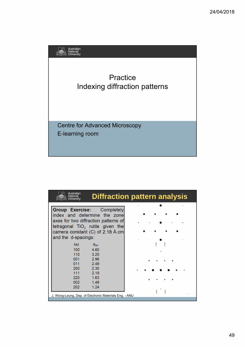
PracticeIndexing diffraction patterns
Centre for Advanced Microscopy
E-learning room
Diffraction pattern analysis
J. Wong-Leung, Dep. of Electronic Materials Eng. - ANU
2.18

24/04/2018
50
Diffraction pattern analysis
J. Wong-Leung, Dep. of Electronic Materials Eng. - ANU
Diffraction pattern analysis
J. Wong-Leung, Dep. of Electronic Materials Eng. - ANU
1.39

24/04/2018
51
Part 3Imaging
Centre for Advanced Microscopy
E-learning room
Contrast
Reproduced from: Transmission Electron Microscopy: A Textbook for Materials ScienceDavid B. Williams and C. Barry Carter
∆

24/04/2018
52
Contrast mechanisms in TEM
Mass thickness contrast
• Formed by incoherent scattering
• Visible without the objective aperture
I
Contrast mechanisms in TEM
Diffraction contrast
I
• Formed by coherent scattering
• Arises from crystals satisfying Bragg’s condition
• Greatly enhanced inserting the objective aperture

24/04/2018
53
Phase contrast-Fresnel Fringes
Intensity profileReproduced: Transmission Electron Microscopy: Physics of Image FormationL. Reimer H. Kohl
Phase contrast-Fresnel Fringes
Fresnel Fringes
In focus:
No dephasingadded by theOL.
Under focus:
= 90º
Over focus:
= - 90º
24/04/2018
54
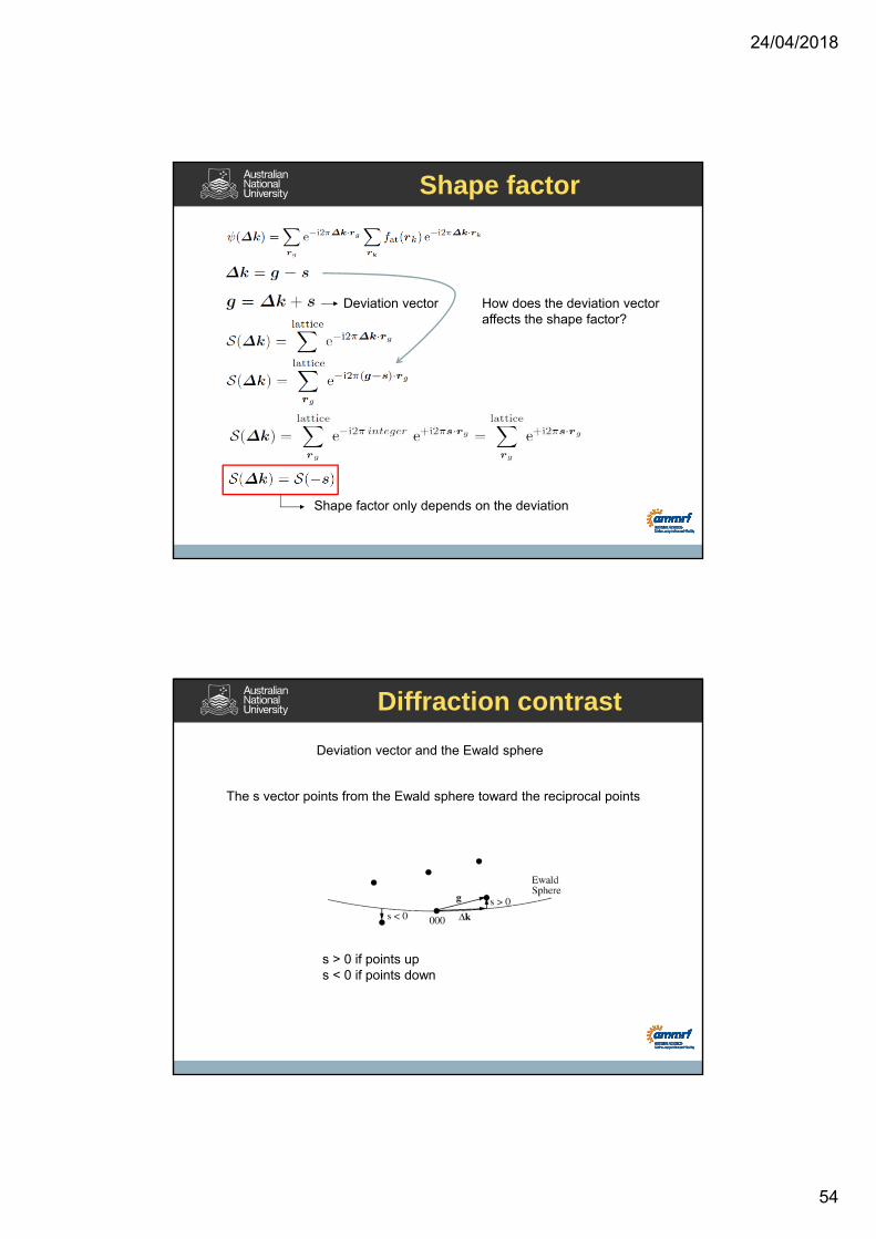
Shape factor
Deviation vector
Shape factor only depends on the deviation
How does the deviation vector affects the shape factor?
Diffraction contrast
Deviation vector and the Ewald sphere
The s vector points from the Ewald sphere toward the reciprocal points
s > 0 if points ups < 0 if points down

24/04/2018
55
Kikuchi lines
Forward peaked incoherent scattering
Incoherent scattering plus coherent (diffraction) Kikuchi lines
Kicuchi lines
Roads through the reciprocal space helps to tilt the sample towards the desired zone-axis
Reproduced from: Brent Fultz · James Howe Transmission Electron Microscopy and Diffractometry of Materials
Kikuchi lines and the deviation
Reproduced from: Brent Fultz · James Howe Transmission Electron Microscopy and Diffractometry of Materials
Reproduced from: Transmission Electron Microscopy: A Textbook for Materials ScienceDavid B. Williams and C. Barry Carter
Position of the Kikuchi line in relation to the diffraction spot changes with s
Setting up a two beam condition
24/04/2018
56
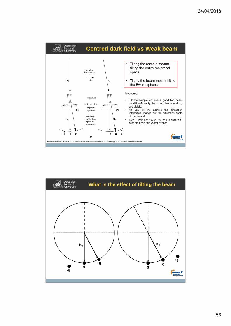
Centred dark field vs Weak beam
• Tilting the sample means tilting the entire reciprocal space.
• Tilting the beam means tilting the Ewald sphere.
Procedure:
• Tilt the sample achieve a good two beamcondition (only the direct beam and +gare visible.
• As you tilt the sample the diffractionintensities change but the diffraction spotsdo not move!
• Now move the vector –g to the centre inorder to have this vector excited.
Reproduced from: Brent Fultz · James Howe Transmission Electron Microscopy and Diffractometry of Materials
What is the effect of tilting the beam
K0K0
-g0
+g+g
-g0
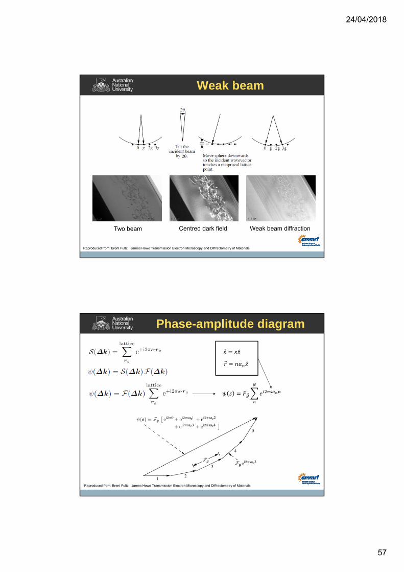
24/04/2018
57
Weak beam
Two beam Centred dark field Weak beam diffraction
Reproduced from: Brent Fultz · James Howe Transmission Electron Microscopy and Diffractometry of Materials
Phase-amplitude diagram
Reproduced from: Brent Fultz · James Howe Transmission Electron Microscopy and Diffractometry of Materials

24/04/2018
58
Thickness fringes (Two-beam)
1
Reproduced from: Brent Fultz · James Howe Transmission Electron Microscopy and Diffractometry of Materials
Thickness fringes
Reproduced from: Brent Fultz · James Howe Transmission Electron Microscopy and Diffractometry of Materials
Two beam condition:Total intensity divided between the direct beam the the diffracted one
Extinction coefficient
For s = 0, period of the thickness fringes is
(dynamical)
For s >> 0, shorter periods(kinetical)
24/04/2018
59
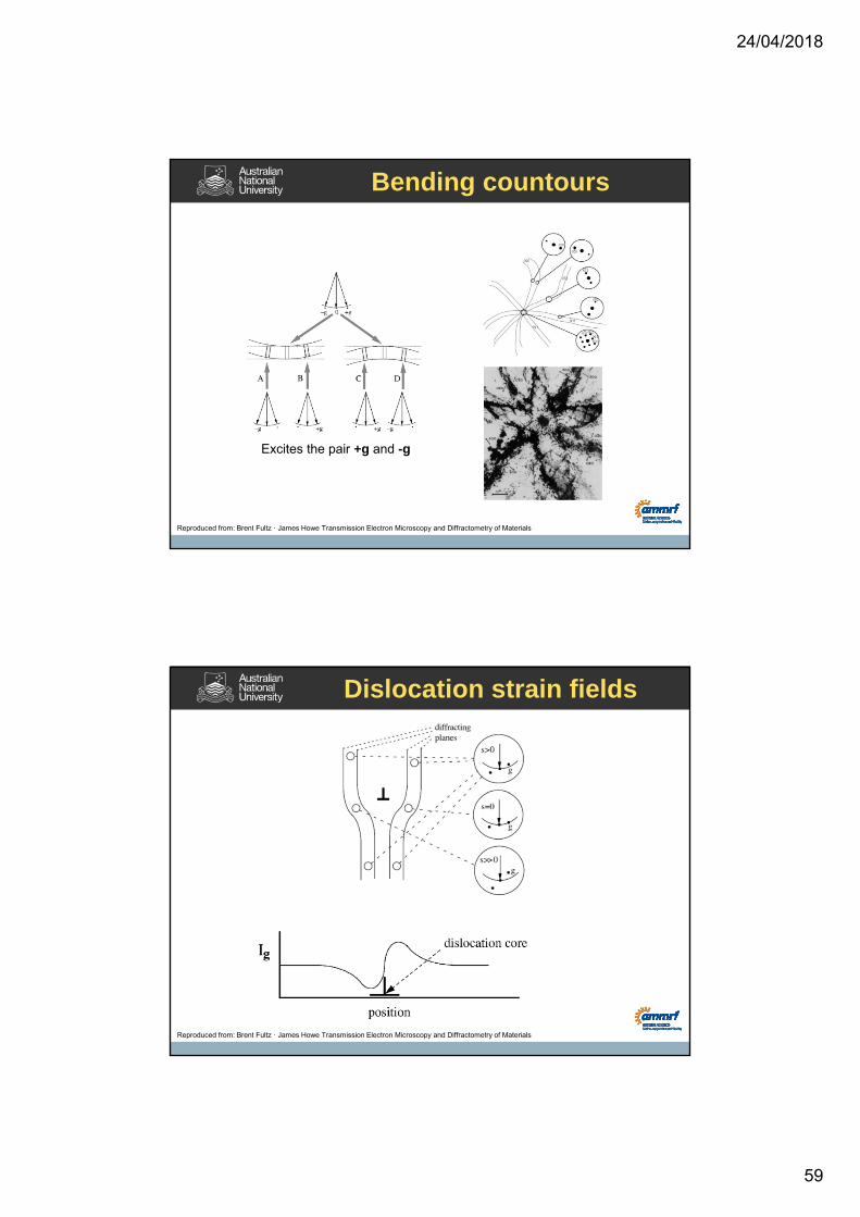
Bending countours
Excites the pair +g and -g
Reproduced from: Brent Fultz · James Howe Transmission Electron Microscopy and Diffractometry of Materials
Dislocation strain fields
Reproduced from: Brent Fultz · James Howe Transmission Electron Microscopy and Diffractometry of Materials

24/04/2018
60
High Resolution TEM
High resolution imaging (phase contrast)
Objectives:
• Know that High Resolution (HR) TEM microscopy is only possible for very thin crystals within the limits in which the Weak Phase Object Approximation is valid.
• Realize HR images can only be obtained if great care in tilting to a zone axis and aligning the aperture is taken.
• Learn that the Contrast Transfer Function can be used to describe the imaging characteristics of the microscope.
• Understand that contrast in HR images cannot be directly assessed without image simulation.

24/04/2018
61
HRTEM
In “high-resolution” transmission electron microscopy (HRTEM or HREM) thephase of the diffracted electron wave is preserved and interferes constructively ordestructively with the phase of the transmitted wave. This technique of “phase-contrast imaging” is used to form images of columns of atoms.
• Electrons that pass between atoms traverse the crystal withminimum change in Intensity.
• Electrons that pass through the columns of atoms undergo largechanges in its intensity and its exit phase changes.
• The information preserved in phase of the waveinterfering produces the phase contrast.
• A objective aperture large enough to allow for boththe direct beam and the g vectors is a requirement
HRTEM
Sb2S3 crystal
• High resolution is not looking at atoms.
• It is a result of phase contrast from theinterference of electrons with columns of atoms.
• The resulting intensity 2D intensity distributionreflects the atomic arrangement in the sampleand therefore rendering atomic resolution.
24/04/2018
62
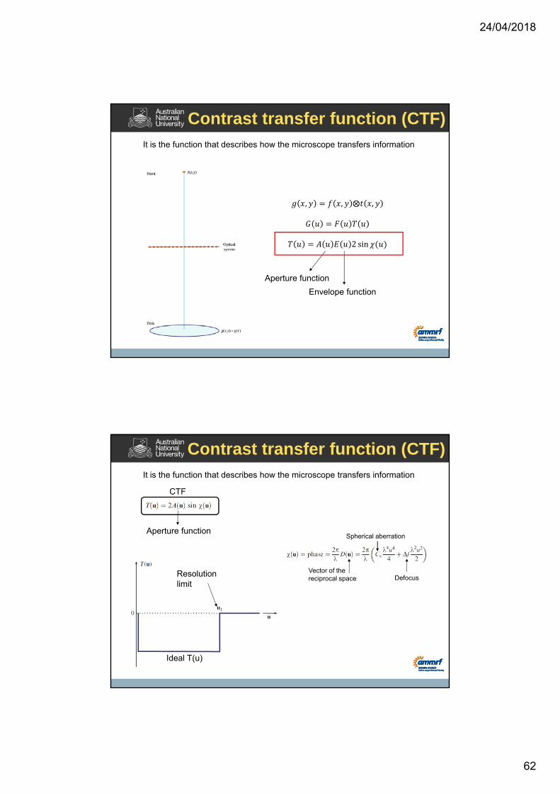
Contrast transfer function (CTF)
, , ⨂ ,
2 sin
Aperture function
Envelope function
It is the function that describes how the microscope transfers information
It is the function that describes how the microscope transfers information
CTF
Aperture functionSpherical aberration
DefocusVector of the reciprocal space
Ideal T(u)
Resolution limit
Contrast transfer function (CTF)

24/04/2018
63
Contrast Transfer Function
Contrast inversion
J. Wong-Leung, Dep. of Electronic Materials Eng. - ANU
24/04/2018
64
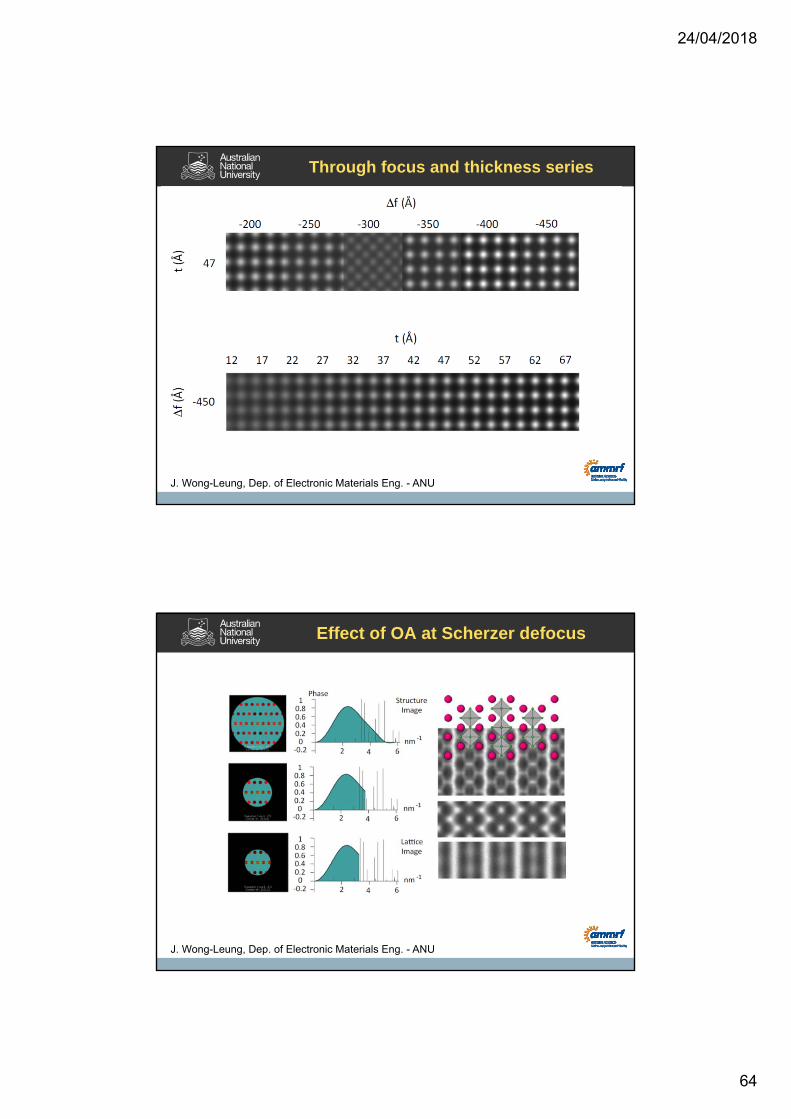
Through focus and thickness series
J. Wong-Leung, Dep. of Electronic Materials Eng. - ANU
Effect of OA at Scherzer defocus
J. Wong-Leung, Dep. of Electronic Materials Eng. - ANU
24/04/2018
65
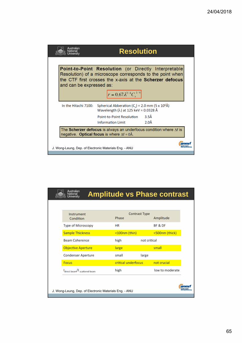
Resolution
J. Wong-Leung, Dep. of Electronic Materials Eng. - ANU
Amplitude vs Phase contrast
J. Wong-Leung, Dep. of Electronic Materials Eng. - ANU

24/04/2018
66
FFT and CTFf = 0 f = - 500 nm f = 500 nm
Astigmatism

24/04/2018
67
Summary
• The optimum focus condition for HR is not at ‘optical’ focus but in anunderfocus condition known as the Scherzer (de)focus.
• The contrast in HR images is strongly dependent on defocus (just a click ortwo on the TEM panel!).
• Atoms are neither black or white in HR images. Atoms in a thin crystal modifythe phase of the electron wave in ways that may fortuitously result in a‘structure’ image where atomic columns have darker contrast.
• Through-focus and through-thickness series can be used to monitor changes inphase contrast
Summary
• Bright field (BF) and dark field (DF) imaging are less demanding than high resolution (HR) microscopy .
• BF and DF microscopy are based on excluding scattered electrons.
• HR microscopy is based on including as many beams as feasible and examining the amplitude variation due to phase shifting.
• HR images can sometimes be interpreted in terms of atomic scale potentials.
• All imaging modes require pre-alignment of the specimen in diffraction mode.
24/04/2018
68
Part 4EDS and STEM
Centre for Advanced Microscopy
E-learning room
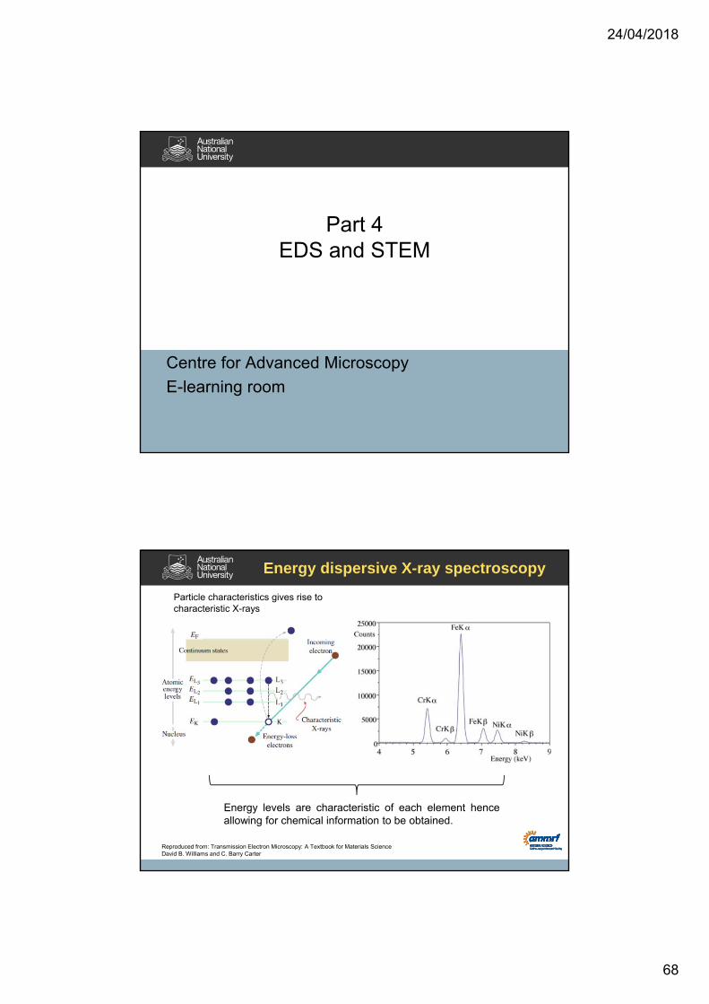
Energy dispersive X-ray spectroscopy
Particle characteristics gives rise to characteristic X-rays
Reproduced from: Transmission Electron Microscopy: A Textbook for Materials ScienceDavid B. Williams and C. Barry Carter
Energy levels are characteristic of each element henceallowing for chemical information to be obtained.

24/04/2018
69
Energy dispersive X-ray spectroscopy
Reproduced from: Transmission Electron Microscopy: A Textbook for Materials ScienceDavid B. Williams and C. Barry Carter
Reproduced from: Brent Fultz · James Howe Transmission Electron Microscopy and Diffractometry of Materials
In EDS spectrum, the x-ray peaks from different elements have intensities that depend on:
1) The path and energy of the high-energy electron passing through the sample;
2) The ionization cross-sections of the elements;3) The fluorescence yields;4) The probabilities that the emitted x-rays are seen by the detector;
Energy dispersive X-ray spectroscopy
15 kV, Bulk 200 kV, 100 nm thick film
C
Pb
24/04/2018
70
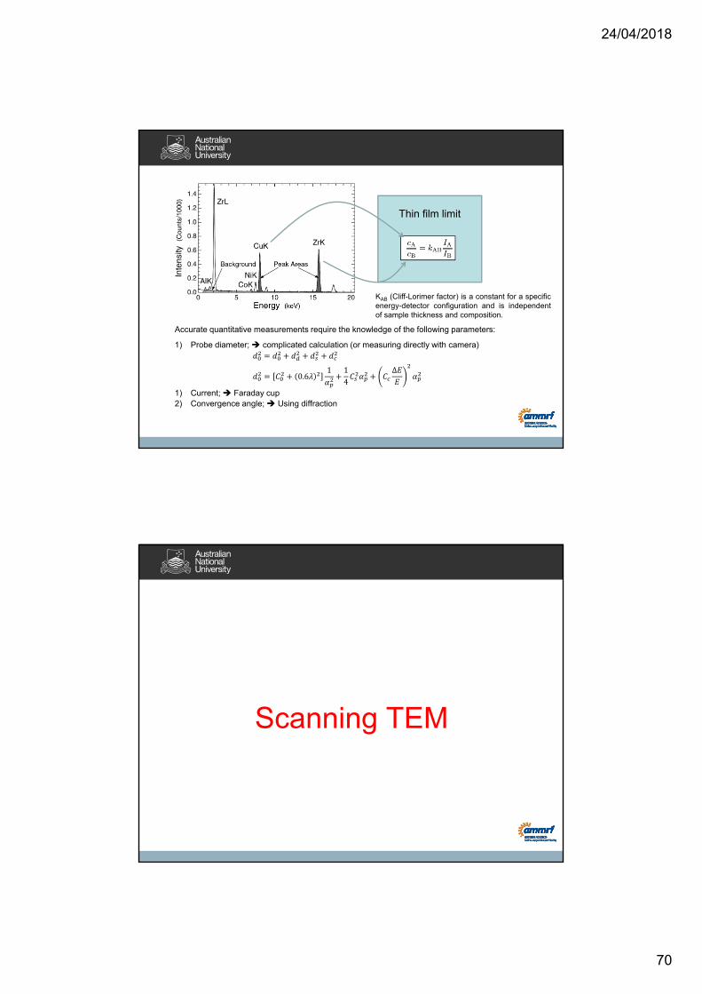
Accurate quantitative measurements require the knowledge of the following parameters:
1) Probe diameter; complicated calculation (or measuring directly with camera)
0.61 1
4Δ
1) Current; Faraday cup2) Convergence angle; Using diffraction
Thin film limit
KAB (Cliff-Lorimer factor) is a constant for a specificenergy-detector configuration and is independentof sample thickness and composition.
Scanning TEM
24/04/2018
71
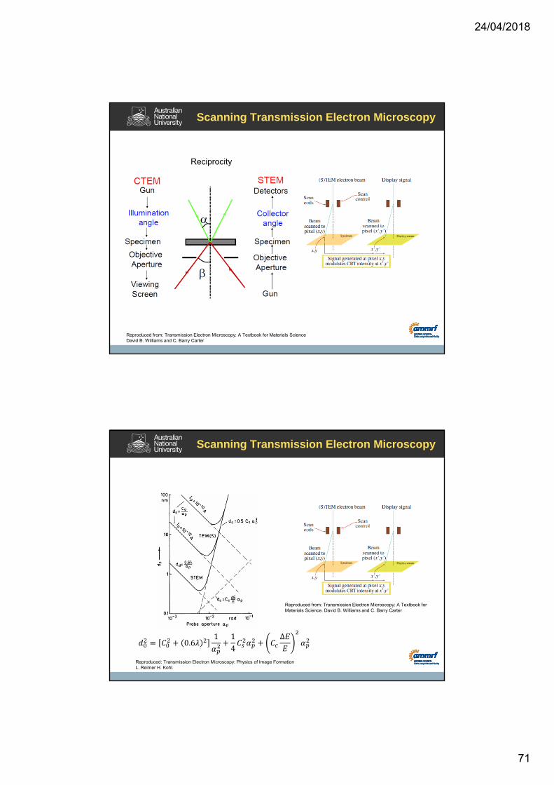
Scanning Transmission Electron Microscopy
Reciprocity
Reproduced from: Transmission Electron Microscopy: A Textbook for Materials ScienceDavid B. Williams and C. Barry Carter
Scanning Transmission Electron Microscopy
Reproduced from: Transmission Electron Microscopy: A Textbook for Materials Science. David B. Williams and C. Barry Carter
0.61 1
4Δ
Reproduced: Transmission Electron Microscopy: Physics of Image FormationL. Reimer H. Kohl.

24/04/2018
72
Scanning Transmission Electron Microscopy
Reproduced from: Transmission Electron Microscopy: A Textbook for Materials ScienceDavid B. Williams and C. Barry Carter
Ronchigram
24/04/2018
73
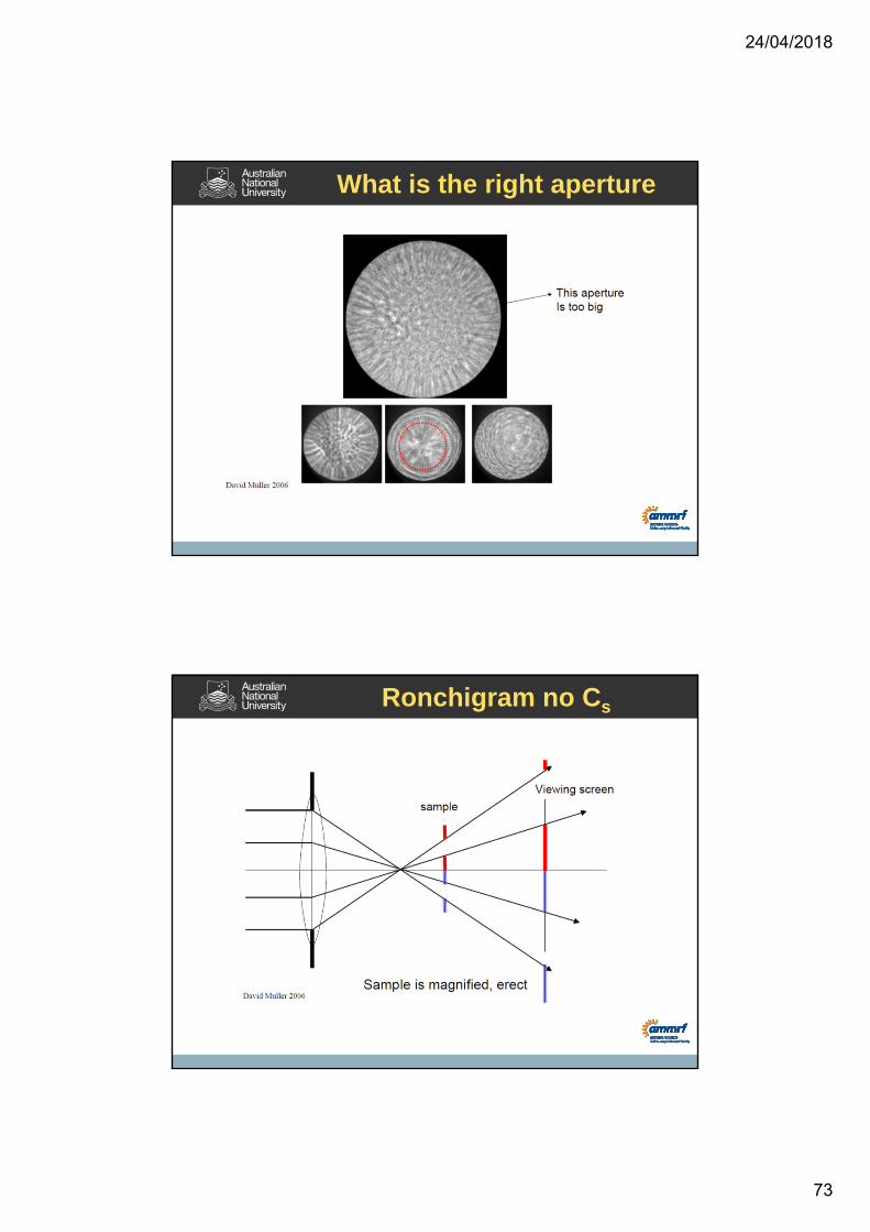
What is the right aperture
Ronchigram no Cs
24/04/2018
74
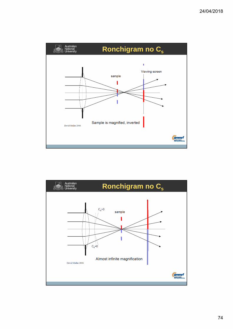
Ronchigram no Cs
Ronchigram no Cs
24/04/2018
75
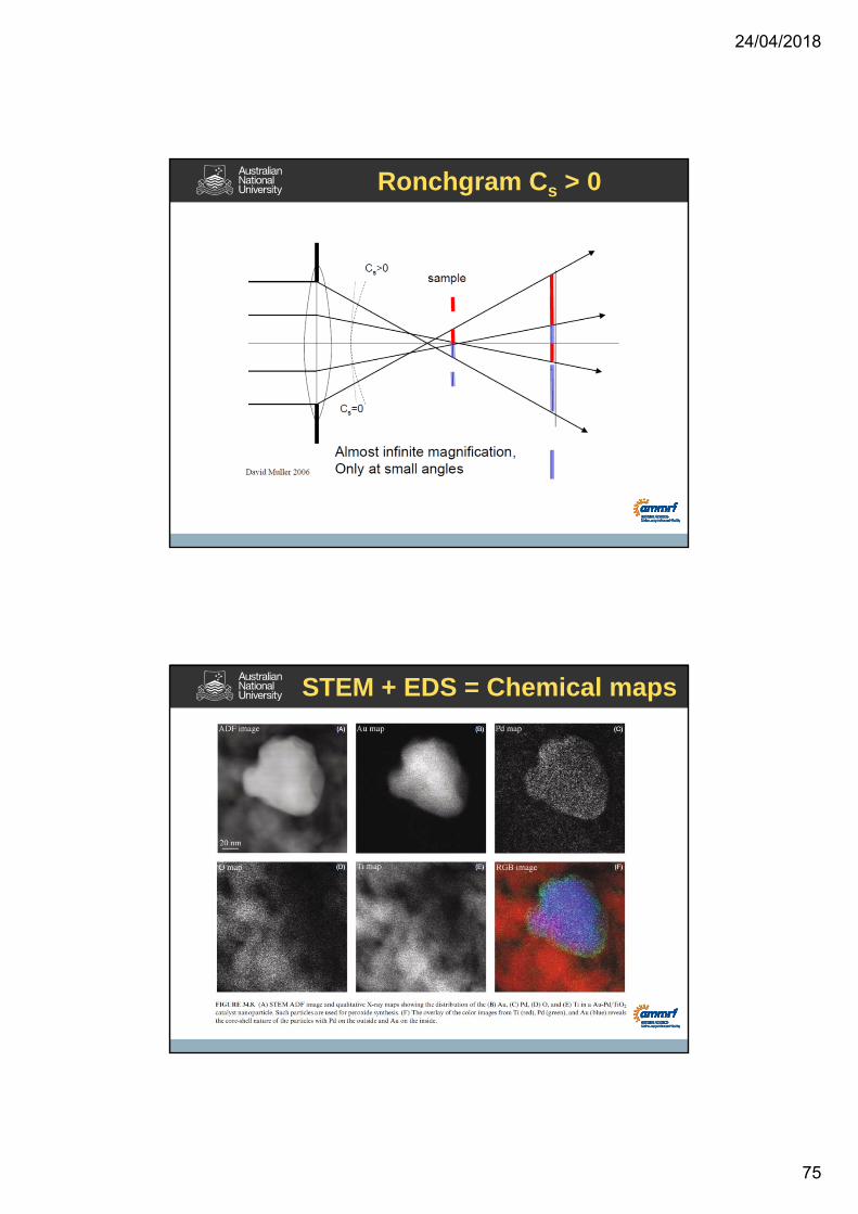
Ronchgram Cs > 0
STEM + EDS = Chemical maps