Embed Size (px)
Citation preview

Chapter 4
UEEP2613
Microelectronic Fabrication
Oxidation

Prepared by
Dr. Lim Soo King
24 Jun 2012
- i -
Chapter 4 ..........................................................................................113
Oxidation ..........................................................................................113
4.0 Introduction ............................................................................................ 113
4.1 Chemistry of Silicon Dioxide Formation ............................................. 115
4.2 Application of Silicon Dioxide ............................................................... 116
4.3 Factors Influencing the Growth of Silicon Dioxide ............................ 119
4.4 Analysis of Silicon Dioxide Growth ...................................................... 123
4.5 Quality of Silicon Dioxide ...................................................................... 127
Exercises ........................................................................................................ 128
Bibliography ................................................................................................. 130
- ii -
Figure 4.1: Oxidation process silicon ............................................................................... 114 Figure 4.2: Volume expansion of silicon dioxide ............................................................ 114 Figure 4.3: Schematic of a basic oxidation furnace ......................................................... 115 Figure 4.4: Silicon dioxide as diffusion mask .................................................................. 116 Figure 4.5: Screen oxide used in ion implantation ........................................................... 117
Figure 4.6: Pad oxide and barrier oxide in STI process ................................................... 117 Figure 4.7: LOCOS process ............................................................................................. 118 Figure 4.8: Process step showing shallow trench isolation structure ............................... 118 Figure 4.9: Process step of deep filled trench with LOCOS ............................................ 119 Figure 4.10: Silicon oxide thickness with time of growth.................................................. 120
Figure 4.11: Illustration of the rate of silicon dioxide formation between wet and dry
methods .......................................................................................................... 121 Figure 4.12: (a) Depletion effect of p-type silicon and (b) pile-up effect of dopant for n-
type silicon ..................................................................................................... 122 Figure 4.13: The model for describing thermal oxidation .................................................. 123 Figure 4.14: Activation energy and pre-exponentials constant various oxidation processes
for (111) silicon. All C2 values should be divided by 1.68 for (100) silicon . 127 Figure 4.15: The value of B and B/A versus temperature for dry oxygen and stream
oxidation methods .......................................................................................... 127
Figure 4.16: The charges associated with thermal oxide ................................................... 128

- 113 -
Chapter 4
Oxidation
_____________________________________________
4.0 Introduction
Silicon dioxide SiO2 is a very good dielectric material. Its dielectric constant is
3.9. Silicon dioxide is used mainly for masking where dopant cannot be
diffused, passivation, and insulation. Thus, oxidation of silicon is necessary
throughout the modern integrated circuit fabrication process. Producing high
quality IC’s requires not only an understanding of the basic oxidation
mechanism but ability to form a high quality oxide in a controlled and
repeatable manner is important. In addition to ensure the reliability of the ICs
the electrical properties of the oxide must understand.
Oxidation is one of the most important thermal processes beside diffusion,
chemical vapor deposition CVD etc. It is an adding oxygen process to silicon
wafer to form silicon dioxide on the surface of wafer. Silicon is very reactive
with oxygen. Thus, in nature most silicon exists in the form of silicon dioxide
such as quartz and sand. Silicon dioxide is a dense material that fully covers the
surface of silicon. To continue the oxidation, oxygen molecules have to diffuse
across the oxide layer to reach the silicon atoms underneath and react with
them. When bare silicon is exposed to the atmosphere, it reacts almost
immediately with oxygen or moisture in the air to form a thin layer of silicon
dioxide of about 10 to 20o
A called native oxide. This thickness of silicon dioxide
is sufficient enough to stop the further oxidation of the silicon at room
temperature due to low diffusivity. Figure 4.1 illustrates the oxidation process
of silicon. As the process progress, the silicon-silicon dioxide interface of the
original silicon has been shifted inward, while the oxide is expanded outward.
In the constrained environment, the ratio of expansion is 1:0.45.
One silicon atom is used to form one molecule of silicon dioxide SiO2.
Based on the densities of silicon NSi and silicon dioxide Nox, which are
4.99x10²²
cm-3
and 2.27x10²²
cm-3
respectively, the recession is 45.5% meaning
every unit thickness of oxide formed required approximately 0.45 unit thickness
of silicon.

04 Oxidation
- 114 -
Figure 4.1: Oxidation process silicon
In oxidation process, oxygen is in gas phase and silicon is in solid form.
Therefore, while silicon dioxide is growing, it consumes the substrate silicon
and the film grows into the silicon substrate. As the result, the volume of at the
silicon-silicon dioxide interface is expanded. Figure 4.2 illustrates the expanded
silicon dioxide at the interface.
(a) Unit of silicon dioxide (b) Unconstrained expansion (c) Constrained expansion
Figure 4.2: Volume expansion of silicon dioxide
Semiconductor can be oxidized by various methods that include thermal
oxidation, electrochemical anodization, and plasma enhanced chemical vapor
deposition PECVD. Among the methods, thermal oxidation is the important
method in today modern integrated circuit fabrication. The basic set-up of a
thermal oxidation furnace is shown in Fig, 4.3. It consists of a resistance heated
furnace, a cylindrical fused-quartz tube containing the wafer held vertically in a
slotted boat, and a source of either pure dry oxygen or pure water vapor. The

04 Oxidation
- 115 -
temperature of oxidation is in the range of 900oC to 1,200
oC with typical gas
flow rate of 1.0 liter per minute.
Figure 4.3: Schematic of a basic oxidation furnace
4.1 Chemistry of Silicon Dioxide Formation
As discussed earlier, oxidation is a process of growing a thin layer of
amorphous silicon dioxide. The process is also termed as chemical vapor
deposition CVD. There are several methods to grow oxide, which are dry and
wet methods. Thermal oxide is grown using oxygen and silicon yields dry
oxide.
Si + O2 SiO2 (4.1)
Silicon dioxide SiO2 can also be grown using hot steam to get wet oxide.
Si + 2H2O SiO2 + 2H2 (4.2)
In terms of quality, dry oxide is better than wet dry due to the rate of growth is
much slower than the corresponding wet oxide growing. If one needs thick
oxide, wet oxide method is preferred due to rate of growth is higher.
Anodic oxide is formed in gaseous or liquid medium by electric field
induced transportation of mobile ion. This method is also termed as low
pressure chemical vapor deposition LPCVD.
Other methods are: low temperature (4000C to 500
0C) chemical vapor
deposition using silane SiH4 and oxygen O2 and high temperature at 1,0000C

04 Oxidation
- 116 -
deposition using tetrachlorosilane SiCl4 with carbon dioxide CO2, oxygen O2,
and water H2O.
SiH4 + O2 SiO2 + 2H2 (4.3)
At this point, it is worth to mention that there is another passivation film, which
is silicon nitride Si3N4 film. This film is also used to passivate semiconductor
device because it acts as a barrier to the diffusion of metal ions, particularly
sodium ions. Reactive sputtering of ammonia or nitrogen is the most common
way to deposit this type of film.
3SiH4 + 4NH3 C900~ 0
Si3N4 + 12H2 (4.4)
or
3SiCl4 + 4NH3 C1200~C550 00
Si3N4 + 12HCl (4.5)
4.2 Application of Silicon Dioxide
Oxidation of silicon is one of the basic processes throughout the IC’s process.
There are many applications for silicon dioxide. One of them is as diffusion
mask. Dopant such as phosphorus and boron have lower diffusion rate in silicon
dioxide than in silicon. Therefore, any etching windows on the masking oxide
layer, one can dope silicon substrate at the designated area by dopant diffusion
process as shown in Fig. 4.4.
Figure 4.4: Silicon dioxide as diffusion mask
Screen oxide is commonly used for ion implantation process. It can help to
prevent silicon contamination by blocking the sputtered photoresist. It can also
minimize the channel effect by scattering the incident ions before they enter a

04 Oxidation
- 117 -
single crystal silicon substrate. The thickness of screen oxide is about 100 to
200o
A . Figure 4.5 illustrates the screen oxide used in ion implantation.
Figure 4.5: Screen oxide used in ion implantation
Silicon dioxide is also used as the barrier layer to prevent contamination of the
silicon substrate before the trench fill the shallow trench isolation STI. Trench
fill is a dielectric CVD process in which undoped silicate glass USG is
deposited to fill the trench for electrical isolation of neighboring transistor.
Since the CVD process always bring a certain level of contamination, silicon
dioxide acts as the barrier to block contamination. Fig. 4.6 illustrates the pad
oxide and the barrier oxide in shallow trench isolation STI process.
(a) Trench etch
(b) Trench refill
(c) Pad oxide and CMP processes
Figure 4.6: Pad oxide and barrier oxide in STI process

04 Oxidation
- 118 -
Localized oxidation of silicon LOCOS has better isolation effect than the
blanket field oxide. LOCOS process uses a thin layer of oxide 200 to 500o
A as
pad layer to buffer the strong tensile stress of the LPCVD nitride. It is illustrated
in Fig. 4.7.
(a) Pad oxidation nitride deposition, and patterning
(b) Oxidation
(c) Pad oxide and nitride strip
Figure 4.7: LOCOS process
Trench isolation either shallow or deep refilled types are used in advanced MOS
and bipolar processes. Shallow trench isolation STI process step is shown in
Fig. 4.8.
(a) Stack and trench etch (b) Pad oxide undercut (c) Liner oxidation
(d) CVD oxide gap filled (e) CMP and HF dip (f) H2PO4 nitride strip
Figure 4.8: Process step showing shallow trench isolation structure
04 Oxidation
- 119 -
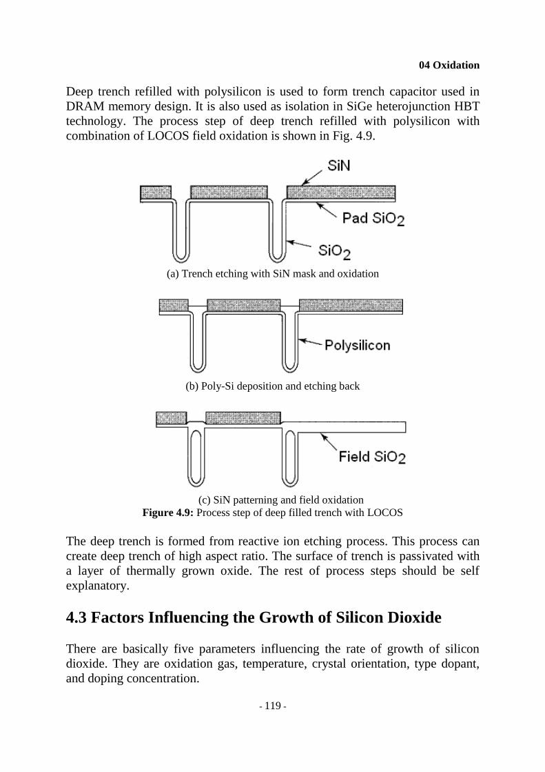
Deep trench refilled with polysilicon is used to form trench capacitor used in
DRAM memory design. It is also used as isolation in SiGe heterojunction HBT
technology. The process step of deep trench refilled with polysilicon with
combination of LOCOS field oxidation is shown in Fig. 4.9.
(a) Trench etching with SiN mask and oxidation
(b) Poly-Si deposition and etching back
(c) SiN patterning and field oxidation
Figure 4.9: Process step of deep filled trench with LOCOS
The deep trench is formed from reactive ion etching process. This process can
create deep trench of high aspect ratio. The surface of trench is passivated with
a layer of thermally grown oxide. The rest of process steps should be self
explanatory.
4.3 Factors Influencing the Growth of Silicon Dioxide
There are basically five parameters influencing the rate of growth of silicon
dioxide. They are oxidation gas, temperature, crystal orientation, type dopant,
and doping concentration.
04 Oxidation
- 120 -
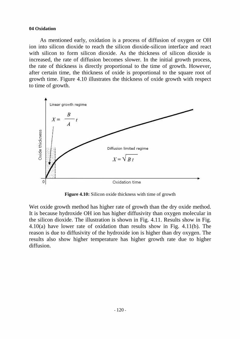
As mentioned early, oxidation is a process of diffusion of oxygen or OH
ion into silicon dioxide to reach the silicon dioxide-silicon interface and react
with silicon to form silicon dioxide. As the thickness of silicon dioxide is
increased, the rate of diffusion becomes slower. In the initial growth process,
the rate of thickness is directly proportional to the time of growth. However,
after certain time, the thickness of oxide is proportional to the square root of
growth time. Figure 4.10 illustrates the thickness of oxide growth with respect
to time of growth.
Figure 4.10: Silicon oxide thickness with time of growth
Wet oxide growth method has higher rate of growth than the dry oxide method.
It is because hydroxide OH ion has higher diffusivity than oxygen molecular in
the silicon dioxide. The illustration is shown in Fig. 4.11. Results show in Fig.
4.10(a) have lower rate of oxidation than results show in Fig. 4.11(b). The
reason is due to diffusivity of the hydroxide ion is higher than dry oxygen. The
results also show higher temperature has higher growth rate due to higher
diffusion.

04 Oxidation
- 121 -
(a) Silicon dry oxidation
(b) Silicon wet oxidation
Figure 4.11: Illustration of the rate of silicon dioxide formation between wet and dry
methods
The grow rate of silicon dioxide is also dependent on the crystal orientation of
the silicon. Silicon crystal of orientation (111) has higher rate of oxide
formation than the (100) orientation due to the fact that the surface density of
(111) orientation is higher than (100) orientation.
04 Oxidation
- 122 -
The rate of silicon dioxide formation is also dependent on the temperature
of the oxidation. The temperature diffusivity follows equation (4.5).
kT/EexpDD ao (4.5)
where Do is the intrinsic diffusivity and Ea is the activation energy.
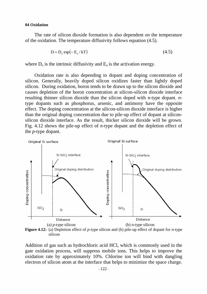
Oxidation rate is also depending to dopant and doping concentration of
silicon. Generally, heavily doped silicon oxidizes faster than lightly doped
silicon. During oxidation, boron tends to be drawn up to the silicon dioxide and
causes depletion of the boron concentration at silicon-silicon dioxide interface
resulting thinner silicon dioxide than the silicon doped with n-type dopant. n-
type dopants such as phosphorus, arsenic, and antimony have the opposite
effect. The doping concentration at the silicon-silicon dioxide interface is higher
than the original doping concentration due to pile-up effect of dopant at silicon-
silicon dioxide interface. As the result, thicker silicon dioxide will be grown.
Fig. 4.12 shows the pile-up effect of n-type dopant and the depletion effect of
the p-type dopant.
(a) p-type silicon (b) n-type silicon
Figure 4.12: (a) Depletion effect of p-type silicon and (b) pile-up effect of dopant for n-type
silicon
Addition of gas such as hydrochloric acid HCl, which is commonly used in the
gate oxidation process, will suppress mobile ions. This helps to improve the
oxidation rate by approximately 10%. Chlorine ion will bind with dangling
electron of silicon atom at the interface that helps to minimize the space charge.

04 Oxidation
- 123 -
Thus, it improves the reliability of the IC. The concentration of chlorine cannot
be too high because too much chlorine introduced in silicon dioxide would
affect the stability of oxide. Extra chlorine ion affects voltage bias of the gate.
4.4 Analysis of Silicon Dioxide Growth
The kinetic of silicon oxidation can be described by the model shown in Fig.
4.13. C0 is the surface concentration of oxidant, in which it has unit
molecule/cm3. The magnitude of C
0 is generally at equilibrium and it is
proportional to the partial pressure of the oxidant adjacent to the surface of
oxide. At temperature 1,000oC and pressure of 1atm, value of C0 is 5.2x10
16cm
-3
for dry oxygen and 3.0x10¹⁹
cm-3
for water vapor.
Figure 4.13: The model for describing thermal oxidation
The flux F1 of oxidant that diffuses through the silicon dioxide layer, which
resulting the concentration CS at the surface of silicon is equal to
)t(d
)CC(D
dx
dCDF
ox
S01
(4.6)

04 Oxidation
- 124 -
where D is the diffusion coefficient of the oxidant and dox(t) is the thickness
already present oxide layer. At the surface of silicon, the oxidant reacts
chemically with silicon. With the assumption that the rate of reaction is
proportional to the concentration CS of oxidant at the surface of silicon, the flux
F2 at the surface is equal to
S2 CF (4.7)
where is the surface reaction rate. At steady state, it is F1 = F2 = F. The flux F
is equal to equation (4.8) after substituting CS from equation (4.7) into equation
(4.6).
)/D()t(d
DCF
ox
0
(4.8)
Let C1 be the number of molecules of oxidant in a unit volume of oxide. The
density of silicon dioxide is 2.2x10²²
cm-3
. One oxygen molecule is added to
each silicon dioxide, while two water molecules are added to each silicon atom.
Therefore, C1 for oxidation for oxygen is 2.2x10²²
cm-3
and for oxidation in
water vapor is 4.4x10²²
cm-3
. With this understanding, the growth rate of oxide
layer is given by
)/D()t(d
C/DC
C
F
dt
)t(dd
ox
10
1
ox
(4.9)
The solution of this equation can be solved by setting the condition that at time t
= 0, the oxide thickness is equal to di. i.e. dox(0) = di. The result is the general
equation for oxidation of silicon, which is
)t(C
DC2)t(d
D2)t(d
1
0ox
2
ox
(4.10)
where )DC2/(C/Dd2d 01i
2
i . It represents a time coordinate shift to account
for the initial oxide layer of thickness di. From equation (4.10), the solution for
oxide thickness dox(t) at time t is equal to
1
DC
)t(C21
D)t(d
1
2
0ox (4.11)
For short time equation (4.11) is deduced to

04 Oxidation
- 125 -
)t(C
C)t(d
1
0ox
(4.12)
For large value of time, equation (4.12) is deduced to
)t(C
DC2)t(d
1
0ox (4.13)
Equation (4.10) can be written in more compact form, which is shown in
equation (4.14).
)t(BAdd ox
2
ox (4.14)
where
D2
A ,1
0
C
DC2B , and
1
0
C
C
A
B . A and B are coefficients depending on
temperature, crystal orientation, activation energy, and gas mixture. These
coefficients shall be dealt from fitting the graph from experimental data. Letting
dox = di at t = 0 and substituting them into equation (4.14), the parameter ,
which is defined as shift in time coordinate to represent the presence of initial
oxide thickness di or time spent to growth the initial thickness of oxide di, is
equal to
B
Add i
2
i (4.15)
Based on the result shown in Fig. 4.10 or Fig. 4.11, the analysis of oxidation
process shows that the grown oxide thickness dox can be approximated by
solving quadratic equation (4.14), which will yield solution for oxide thickness
dox(t) equation (4.16).
1
)B4/(A
)t(1
2
A)t(d
2ox (4.16)
This quadratic equation has two limit forms of the linear and parabolic growth
whereby they are described by equation (4.17) and (4.19) respectively. The
initial phase of oxide growth is a linear process because the time t is small.
Based on equation (4.16), the oxide thickness dox is deduced to
dox(t) = )t(A
B (4.17)

04 Oxidation
- 126 -
This equation is true only if (t+) << B4
A2
, which shall mean a short oxidation
time as discussed earlier.
Based on equation (4.16), oxidation time tl is equal to equation (4.18) if
one assumes that there is no prior grown oxide.
A/B
)t(dt ox
l (4.18)
As time goes on, the process is slow down due to lower diffusivity of oxidation
agent in the already grown silicon dioxide. The thickness dox(t) will follow
equation (4.19) if there is prior grown oxide.
dox(t) = )t(B (4.19)
Equation (4.19) is true only if t >> and t >>B4
A2
, this shall mean that it has
long oxidation time. The time tp of growth for the oxide is
B
)t(dt
2
oxp (4.20)
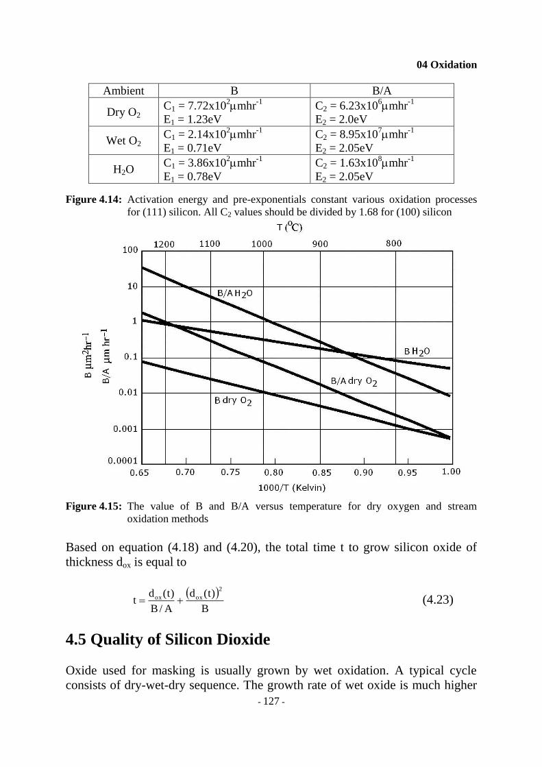
Based on experimental data, the coefficient B and B/A can be described by
Arrhenius expression which are shown in equation (4.21) and (4.22)
respectively.
)kT/Eexp(CB 11 (4.21)
and
)kT/Eexp(CA/B 22 (4.22)
E1 and E2 are activation energies associated with the physical process that B and
B/A are represented. C1 and C2 are pre-exponential constants. These mentioned
constant values for various types of oxidation processes can be obtained from
Fig. 4.14. Alternatively, the value of B and B/A can be obtained from the graph
shown in Fig. 4.15.
04 Oxidation
- 127 -
Ambient B B/A
Dry O2 C1 = 7.72x10
2mhr
-1
E1 = 1.23eV
C2 = 6.23x10⁶mhr
-1
E2 = 2.0eV
Wet O2 C1 = 2.14x10
2mhr
-1
E1 = 0.71eV
C2 = 8.95x10⁷mhr
-1
E2 = 2.05eV
H2O C1 = 3.86x10
2mhr
-1
E1 = 0.78eV
C2 = 1.63x10⁸mhr
-1
E2 = 2.05eV
Figure 4.14: Activation energy and pre-exponentials constant various oxidation processes
for (111) silicon. All C2 values should be divided by 1.68 for (100) silicon
Figure 4.15: The value of B and B/A versus temperature for dry oxygen and stream
oxidation methods
Based on equation (4.18) and (4.20), the total time t to grow silicon oxide of
thickness dox is equal to
B
)t(d
A/B
)t(dt
2
oxox (4.23)
4.5 Quality of Silicon Dioxide
Oxide used for masking is usually grown by wet oxidation. A typical cycle
consists of dry-wet-dry sequence. The growth rate of wet oxide is much higher

04 Oxidation
- 128 -
than growth of dry oxide. However, the quality of dry oxide is higher due to
denser and has breakdown voltage in region of 5 – 10MV/cm. Owing to this fact,
thin oxide is usually grown using dry oxidation.
MOS devices are affected by charges in the oxide and traps at SiO2-Si
interface. The basic classification of these traps and charges are shown in Fig.
4.16. The interface trapped charges Qit are due to the SiO2-Si interface
properties and dependent on the chemical composition of the interface. These
traps are located at SiO2-Si with energy state located within silicon forbidden
band-gap. The fixed charge Qf is located within approximately 3.0nm of the
SiO2-Si interface. Fixed charge is positive and depends on oxidation and
annealing condition. Oxide trapped charge Qot is associated with defects within
silicon dioxide. This charge is created like X-ray radiation or high energy
bombardment. Mobile ionic charges Qm due to contamination from sodium or
other alkali, are mobile within the oxide under raised temperature and high
electric field operation. In this condition the mobile ions are moving forth and
back through the oxide layer and cause threshold voltage shifts.
Figure 4.16: The charges associated with thermal oxide
Exercises
4.1. The densities of silicon NSi and silicon dioxide Nox are 4.99x10²²
cm-3
and
2.27x10²²
cm-3
respectively. Prove that each unit thickness of silicon
dioxide formed, it utilizes 0.45 unit thickness of of silicon.
04 Oxidation
- 129 -
4.2. Name three factors that influencing the oxide growth.
4.3. What is the purpose of screen oxide?
4.4. What is the purpose of growth LOCOS?
4.5. State a reason why hot stream has higher oxidation rate than dry oxygen.
4.6. State the reason why the linear oxidation of (111) orientation is faster
than the (100) orientation silicon crystal.
4.7. HCl is introduced to improve the reliability of oxide by binding with
dangling electron of silicon during oxidation. State the reason why HF
gas cannot be used.
4.8. Calculate the time taken to grow 2m thick oxide using hot stream at
temperature 1,1000C.
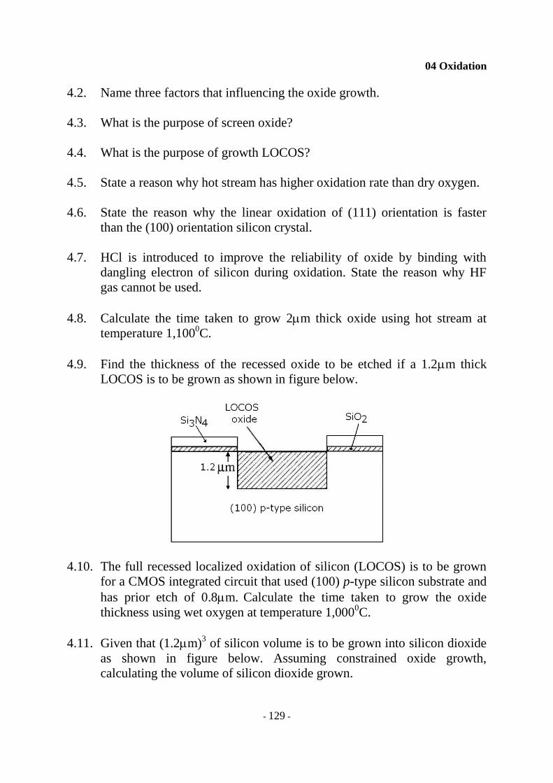
4.9. Find the thickness of the recessed oxide to be etched if a 1.2m thick
LOCOS is to be grown as shown in figure below.
4.10. The full recessed localized oxidation of silicon (LOCOS) is to be grown
for a CMOS integrated circuit that used (100) p-type silicon substrate and
has prior etch of 0.8m. Calculate the time taken to grow the oxide
thickness using wet oxygen at temperature 1,0000C.
4.11. Given that (1.2m)3 of silicon volume is to be grown into silicon dioxide
as shown in figure below. Assuming constrained oxide growth,
calculating the volume of silicon dioxide grown.

04 Oxidation
- 130 -
4.12. Find the thickness of the recessed silicon to be etched if the oxide
structure shown in the figure is to be grown.
Bibliography
1. JD Pummer, MD Del, and Peter Griffin, “Silicon VLSI Technology”
Fundamentals, Practices, and Modeling”, Prentice Hall, 2000.
2. Hong Xiao, “Introduction to Semiconductor Manufacturing Technology”,
Pearson Prentice Hall, 2001.
3. SM Sze, “VLSI Technology”, second edition, McGraw-Hill, 1988.
4. CY Chang and SM Sze, “ULSI Technology”, McGraw-Hill, 1996.
5. Gary S. May and Costas J. Spanos, “Fundamentals of Semiconductor
Manufacturing and Process Control”, IEEE Wiley-Interscience, 2006.

Index
- 131 -
A
Activation energy ............................................... 122 Ammonia ........................................................... 116 Anodic oxide ...................................................... 115 Antimony ........................................................... 122 Arsenic ............................................................... 122
B
Barrier oxide ...................................................... 117 Boron ................................................................. 116
C
Carbon dioxide ................................................... 116 Chemical vapor deposition ................ 113, 115, 117 Chlorine ............................................................. 123 CVD ......................... See Chemical vapor deposition
D
Dielectric constant ............................................. 113 Diffusion ............................................................ 116 Diffusivity ........................................................... 122 Dry oxide ............................................................ 115
E
Electrochemical anodization ............................. 114
F
Fixed charge ....................................................... 128
H
HBT technology .................................................. 119 Hydrochloric acid ............................................... 122
I
Interface trapped charges ................................. 128 Intrinsic diffusivity ............................................. 122
L
Localized oxidation of silicon ..................... 118, 119 LOCOS .................. See Localized oxidation of silicon Low pressure chemical vapor deposition .. 115, 118 LPCVD See Low pressure chemical vapor deposition
M
Memory
Dynamic RAM ................................................. 119 Mobile ionic charge............................................ 128
N
Native oxide ....................................................... 113 Nitrogen ............................................................. 116
O
Oxidation ............................................................ 113 Oxide trapped charge ........................................ 128 Oxygen ............................... 113, 114, 115, 120, 124
P
Pad oxide............................................................ 117 Phosphorus ................................................ 116, 122 Plasma enhanced chemical vapor deposition .... 114 Polysilicon .......................................................... 119
R
Reactive ion etching ........................................... 119 Reactive sputtering ............................................ 116
S
Screen oxide ....................................................... 117 Semiconductor
SiGe ................................................................ 119 Shallow trench isolation ............................. 117, 118 SiGe heterojunction ........................................... 119 Silane .................................................................. 115 Silicon ................................................................. 113 Silicon dioxide .................... 113, 114, 115, 117, 120 Silicon nitride ..................................................... 116 Sodium ....................................................... 116, 128 STI ............................... See Shallow trench isolation
T
Tetrachlorosilane ............................................... 116 Thermal oxide .................................................... 115
U
Undoped silicate glass........................................ 117
W
Wet oxide ........................................................... 115