Embed Size (px)
Citation preview

PRL 96, 036103 (2006) P H Y S I C A L R E V I E W L E T T E R S week ending27 JANUARY 2006
Influence of the Metal Substrate on the Adsorption Properties of Thin Oxide Layers:Au Atoms on a Thin Alumina Film on NiAl(110)
M. Kulawik, N. Nilius,* and H.-J. FreundFritz-Haber-Institut der Max-Planck-Gesellschaft, Faradayweg 4-6, D-14195 Berlin, Germany
(Received 19 July 2005; published 24 January 2006)
0031-9007=
Thin oxide films grown on metal substrates are widely used in surface science to model bulk oxides,assuming their chemical and electronic properties to be similar. In some cases, however, this might not bejustified as the present scanning tunneling microscopy studies demonstrate for Au atoms on a thin aluminafilm on NiAl(110). Au atoms were evaporated onto the oxide film at a sample temperature of �10 K. Atlow coverage, this leads to the formation of one-dimensional clusters with unusually large Au-Audistances of 5.6–6.0 A. A direct interaction between the Au atoms can be excluded, and a substrate-mediated mechanism is supposed instead. This assumption is strengthened by the finding that the Auchains exhibit a preferential orientation: They are almost aligned with the �001� direction of the NiAl(110)substrate, clearly indicating that the metal substrate participates in the binding of the Au atoms.
DOI: 10.1103/PhysRevLett.96.036103 PACS numbers: 68.43.Hn, 68.37.Ef, 68.47.Jn, 73.22.�f
Metal particles on thin oxide films are well establishedin surface science to model heterogeneous catalysts [1–3].These model systems have similar chemical and electronicproperties as real catalysts but are by far less complex andeasier to investigate because of the conductivity of thinfilms in contrast to most bulk oxides. Oxide-film-basedmodel systems are, therefore, well-suited to gain funda-mental understanding on the nature of catalytically activesites and reaction kinetics [4]. Other questions concern thematerial transport on oxide surfaces and aim to determinepreferential adsorption sites, diffusion, nucleation, andcatalytic activity of supported metal atoms.
Commonly, thin oxide films with band gaps similar tothe corresponding bulk oxides (usually wide-gap insula-tors) are supposed to reflect also their chemical propertiesand to be, therefore, suited as model systems for the bulkmaterial. This is justified by a huge amount of experimen-tal evidence [1–4]. However, according to a recent theo-retical work, a generalization of this assumption to allmetal-oxide-film systems has to be doubted [5]. The au-thors compared the adsorption of Au atoms on bulk MgOwith that on MgO films on Mo(100). While Au atoms werefound to be neutral on bulk MgO, they appeared to benegatively charged on thin MgO films. The effect wasascribed to electron tunneling from the underlying metalsubstrate [5,6], induced by the high electron affinity of Au(2.31 eV). This theoretical study suggests that carefulanalysis is necessary to evaluate the suitability of thin filmsas model support. However, to our knowledge, experimen-tal evidence for such deviating properties of thin oxidefilms has not been reported yet. In this Letter, we providescanning tunneling microscopy (STM) studies whichclearly reveal an influence of the limited film thicknesson the adsorption behavior of an oxide film. For thatpurpose, we investigated the nucleation of Au atoms on a5 A thin alumina film on NiAl(110) [7,8] with STM. Thefilm has a band gap of �8 eV, which is similar to that ofbulk alumina (8.8 eV) [8]. Its structure was resolved only
06=96(3)=036103(4)$23.00 03610
recently [9], revealing the stoichiometry to be Al10O13 andopening new possibilities for the understanding of theinteraction with metal adatoms. Surprisingly, well-definedone-dimensional Au clusters are found upon deposition at�10 K. Their orientation clearly indicates an involvementof the NiAl substrate in the binding of the Au atoms.
The measurements were performed in ultrahigh vacuum,using a home-built STM operated at 5 K [10]. The cleanNiAl(110) surface is prepared by repeated cycles of Ar�
sputtering and annealing to 1000 �C. Subsequent dosing ofO2 at 280 �C and annealing to 800 �C leads to the forma-tion of a thin, crystalline alumina film [7]. Au is evaporatedfrom a gold-covered tungsten wire onto the sample, whichhas then a temperature of �10 K.
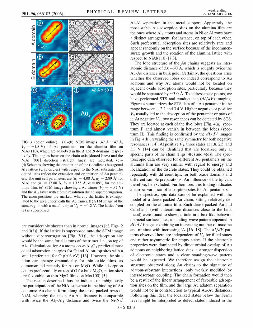
A typical coverage used for our studies is shown in theSTM image in Fig. 1. The image reveals the presence ofboth Au monomers and clusters, which form even at lowcoverage because Au atoms can move on the surface priorto thermalization. While Au aggregates are imaged with alarge apparent diameter at positive sample bias VS, theyappear much smaller at negative VS, allowing the determi-nation of their internal structure. The majority are Audimers with different orientations, but also small clustersare observed. Surprisingly, many of these clusters are one-dimensional (1D) chains. Figure 2 shows STM images of aAu monomer and such self-assembled Au chains with amaximum length of 22.5 A. Longer chains have not beenobserved. The images are recorded at negative VS, wherebyVS is chosen well above (left side) and close to (middle) thehighest occupied state of the Au chains, which was deter-mined by scanning tunneling spectroscopy (STS). On theleft-hand side, the chains appear with a uniform height of�4 �A. The imaging properties change dramatically in thecase of resonant tunneling into the electronic states of thechain (middle). The apparent height of the chains is thenincreased by 1–2 A. Furthermore, the chains show a dis-tinct substructure, consisting of 3–5 lobes. These lobes areseparated by 5.6–6.0 A, which corresponds to the double
3-1 © 2006 The American Physical Society
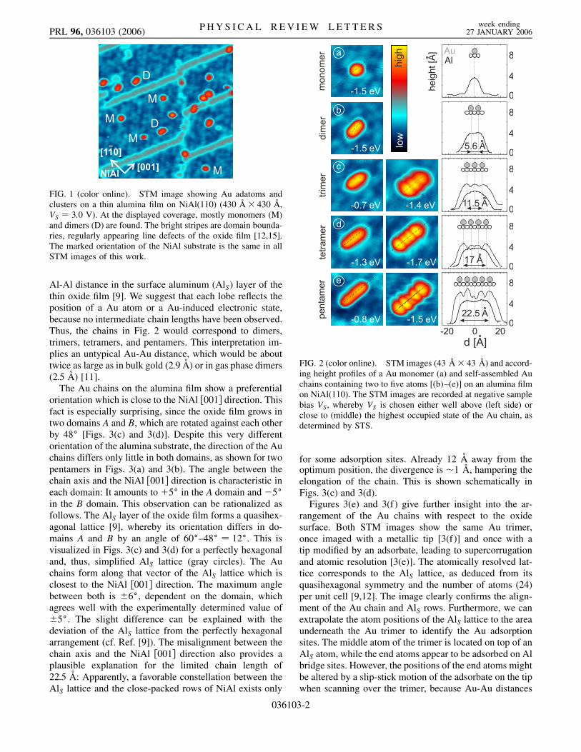
FIG. 2 (color online). STM images (43 �A 43 �A) and accord-ing height profiles of a Au monomer (a) and self-assembled Auchains containing two to five atoms [(b)–(e)] on an alumina filmon NiAl(110). The STM images are recorded at negative samplebias VS, whereby VS is chosen either well above (left side) orclose to (middle) the highest occupied state of the Au chain, asdetermined by STS.
FIG. 1 (color online). STM image showing Au adatoms andclusters on a thin alumina film on NiAl(110) (430 �A 430 �A,VS � 3:0 V). At the displayed coverage, mostly monomers (M)and dimers (D) are found. The bright stripes are domain bounda-ries, regularly appearing line defects of the oxide film [12,15].The marked orientation of the NiAl substrate is the same in allSTM images of this work.
PRL 96, 036103 (2006) P H Y S I C A L R E V I E W L E T T E R S week ending27 JANUARY 2006
Al-Al distance in the surface aluminum (AlS) layer of thethin oxide film [9]. We suggest that each lobe reflects theposition of a Au atom or a Au-induced electronic state,because no intermediate chain lengths have been observed.Thus, the chains in Fig. 2 would correspond to dimers,trimers, tetramers, and pentamers. This interpretation im-plies an untypical Au-Au distance, which would be abouttwice as large as in bulk gold (2.9 A) or in gas phase dimers(2.5 A) [11].
The Au chains on the alumina film show a preferentialorientation which is close to the NiAl �001� direction. Thisfact is especially surprising, since the oxide film grows intwo domains A and B, which are rotated against each otherby 48� [Figs. 3(c) and 3(d)]. Despite this very differentorientation of the alumina substrate, the direction of the Auchains differs only little in both domains, as shown for twopentamers in Figs. 3(a) and 3(b). The angle between thechain axis and the NiAl �001� direction is characteristic ineach domain: It amounts to �5� in the A domain and �5�
in the B domain. This observation can be rationalized asfollows. The AlS layer of the oxide film forms a quasihex-agonal lattice [9], whereby its orientation differs in do-mains A and B by an angle of 60�–48� � 12�. This isvisualized in Figs. 3(c) and 3(d) for a perfectly hexagonaland, thus, simplified AlS lattice (gray circles). The Auchains form along that vector of the AlS lattice which isclosest to the NiAl �001� direction. The maximum anglebetween both is �6�, dependent on the domain, whichagrees well with the experimentally determined value of�5�. The slight difference can be explained with thedeviation of the AlS lattice from the perfectly hexagonalarrangement (cf. Ref. [9]). The misalignment between thechain axis and the NiAl �001� direction also provides aplausible explanation for the limited chain length of22.5 A: Apparently, a favorable constellation between theAlS lattice and the close-packed rows of NiAl exists only
03610
for some adsorption sites. Already 12 A away from theoptimum position, the divergence is �1 �A, hampering theelongation of the chain. This is shown schematically inFigs. 3(c) and 3(d).
Figures 3(e) and 3(f) give further insight into the ar-rangement of the Au chains with respect to the oxidesurface. Both STM images show the same Au trimer,once imaged with a metallic tip [3(f)] and once with atip modified by an adsorbate, leading to supercorrugationand atomic resolution [3(e)]. The atomically resolved lat-tice corresponds to the AlS lattice, as deduced from itsquasihexagonal symmetry and the number of atoms (24)per unit cell [9,12]. The image clearly confirms the align-ment of the Au chain and AlS rows. Furthermore, we canextrapolate the atom positions of the AlS lattice to the areaunderneath the Au trimer to identify the Au adsorptionsites. The middle atom of the trimer is located on top of anAlS atom, while the end atoms appear to be adsorbed on Albridge sites. However, the positions of the end atoms mightbe altered by a slip-stick motion of the adsorbate on the tipwhen scanning over the trimer, because Au-Au distances
3-2
Au3
Au3
x
x
x
+5°
-5°
[001]
[110]
NiAl
Al O10 13
[001]
[110]
NiAl
e f
B d
omai
n
c
d
Ado
mai
n
a
b
Al O10 13
-6°
+6°
AlS
AlS
42 Å x 50 Å
FIG. 3 (color online). (a)–(b) STM images (47 �A 47 �A,VS � �1:8 V) of Au pentamers on the alumina film onNiAl(110), which are adsorbed in the A and B domains, respec-tively. The angles between the chain axis (dotted lines) and theNiAl �001� direction (straight lines) are indicated. (c)–(d) Schemes showing the orientation of the (idealized) hexagonalAlS lattice (gray circles) with respect to the NiAl substrate. Thedotted lines reflect the extension and orientation of Au pentam-ers. The unit cell parameters are (a1 � 4:08 �A, a2 � 2:89 �A) forNiAl and (b1 � 17:88 �A, b2 � 10:55 �A, � � 89�) for the alu-mina film. (e) STM image showing a Au trimer (VS � �0:7 V)and the AlS layer with atomic resolution due to supercorrugation.The atom positions are marked, whereby the lattice is extrapo-lated to the area underneath the Au trimer. (f) STM image of thesame region with a metallic tip at VS � �1:2 V. The lattice from(e) is superposed.
PRL 96, 036103 (2006) P H Y S I C A L R E V I E W L E T T E R S week ending27 JANUARY 2006
are considerably shorter than in normal images [cf. Figs. 2and 3(f)]. If the lattice is superposed onto the STM imagewithout supercorrugation [Fig. 3(f)], the adsorption sitewould be the same for all atoms of the trimer, i.e., on top ofAlS. Calculations for Au atoms on �-Al2O3 predict almostequal adsorption energies for O and Al on-top sites with asmall preference for O (0.03 eV) [13]. However, the situ-ation can change dramatically for thin oxide films, asdemonstrated recently for Au on MgO. While adsorptionoccurs preferentially on top of O for bulk MgO, cation sitesare favorable on thin MgO films on Mo(100) [5].
The results described thus far indicate unambiguouslythe participation of the NiAl substrate in the binding of Auadatoms: Au chains form along the close-packed rows ofNiAl, whereby the mean Au-Au distance is compatiblewith twice the AlS-AlS distance and twice the Ni-Ni=
03610
Al-Al separation in the metal support. Apparently, themost stable Au adsorption sites on the alumina film arethe ones where AlS atoms and atoms in Ni or Al rows havea distinct arrangement, for instance, on top of each other.Such preferential adsorption sites are relatively rare andappear randomly on the surface because of the incommen-surate growth and the rotation of the alumina lattice withrespect to NiAl(110) [7,8].
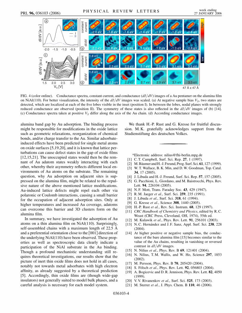
The lobe structure of the Au chains suggests an inter-atomic distance of 5.6–6.0 A, which is roughly twice theAu-Au distance in bulk gold. Certainly, the questions arisewhether the observed lobes do indeed correspond to Auadatoms and why Au atoms would not be located onadjacent oxide adsorption sites, particularly because theywould be separated by�3:0 �A. To address these points, wehave performed STS and conductance (dI=dV) imaging.Figure 4 summarizes the STS data of a Au pentamer in therange between �2:2 and 3.4 V. Higher negative or positiveVS usually led to the desorption of the pentamer or parts ofit. At negative VS, two resonances can be detected by STS.They are located at each of the five lobes [Fig. 4(a), spec-trum I] and almost vanish in between the lobes (spec-trum II). This finding is confirmed by the dI=dV imagesin Fig. 4(b), revealing the same symmetry for both negativeresonances [14]. At positive VS, three states at 1.8, 2.5, and3.3 V [14] can be identified that are localized only atspecific parts of the chain [Figs. 4(c) and 4(d)]. The spec-troscopic data observed for different Au pentamers on thealumina film are very similar with regard to energy andlocalization of the discrete states. They could be obtainedrepeatedly with different tips, for both oxide domains anddifferent sample preparations. An influence of the tip can,therefore, be excluded. Furthermore, this finding indicatesa narrow variation of adsorption sites for Au pentamers.
The spectroscopic data cannot be explained with themodel of a dense-packed Au chain, sitting relatively de-coupled on the alumina film. Such dense-packed Au andCu chains (with interatomic distances close to the bulkmetal) were found to show particle-in-a-box-like behavioron metal surfaces; i.e., a standing-wave pattern appeared indI=dV images exhibiting an increasing number of maximaand minima with increasing VS [16–18]. The dI=dV pat-terns observed here are independent of VS for filled statesand rather asymmetric for empty states. If the electronicproperties were dominated by direct orbital overlap of Auadatoms on neighboring lattice sites, a stronger dispersionof electronic states and a clear standing-wave patternwould be expected. We therefore assign the electronicstructure observed along Au chains to the signature ofadatom-substrate interactions, only weakly modified byinteradsorbate coupling. The chain formation would thenbe a result of the linear arrangement of favorable adsorp-tion sites on the film, and the large Au adatom separationwould not be in contradiction to typical Au-Au distances.Following this idea, the localized states below the Fermilevel might be interpreted as defect states induced in the
3-3
d
b
dI/d
Vco
nsta
ntcu
rren
t
-1.2 eV
-1.2 eV
-1.0 eV
-1.0 eV
-0.8 eV
-0.8 eV
-1.8 eV
-1.8 eV
-1.6 eV
-1.6 eV
-1.4 eV
-1.4 eV
-2.0 eV
-2.0 eV
3.3 eV3.1 eV2.9 eV2.7 eV2.5 eV2.3 eV
3.3 eV3.1 eV2.9 eV2.7 eV2.5 eV2.3 eV
1.8 eV
1.8 eV
V [V]S
c
-2.0 -1.5 -1.0 -0.5
dI/d
V [a
.u.]
III
III
a
dI/d
Vco
nsta
ntcu
rren
t
low
high
b
d1.5 2.0 2.5 3.0
dI/d
V [a
.u.]
a
b
c abc
47 Å x 47 Å
FIG. 4 (color online). Conductance spectra, constant current, and conductance (dI=dV) images of a Au pentamer on the alumina filmon NiAl(110). For better visualization, the intensity of the dI=dV images was scaled. (a) At negative sample bias VS, two states aredetected, which are localized at each of the five lobes visible in the inset (position I). In between the lobes, nodal planes with stronglyreduced conductance are observed (position II). The symmetry of these states is also reflected in the dI=dV images of (b) [14].(c) Conductance spectra taken at positive VS differ along the axis of the Au chain. (d) According conductance images.
PRL 96, 036103 (2006) P H Y S I C A L R E V I E W L E T T E R S week ending27 JANUARY 2006
alumina band gap by Au adsorption. The binding processmight be responsible for modifications in the oxide latticesuch as geometric relaxations, reorganization of chemicalbonds, and/or charge transfer to the Au. Similar adsorbate-induced effects have been predicted for single metal atomson oxide surfaces [5,19,20], and it is known that lattice per-turbations can cause defect states in the gap of oxide films[12,15,21]. The unoccupied states would then be the rem-nant of Au adatom states weakly interacting with eachother, whereby their asymmetry reflects different local en-vironments of Au atoms on the substrate. The remainingquestion, why Au adsorption on adjacent sites is sup-pressed on the alumina film, might be related to the repul-sive nature of the above mentioned lattice modifications.Au-induced lattice defects might repel each other viapolaronic or Coulomb interactions, causing a small barrierfor the occupation of adjacent adsorption sites. Only athigher temperatures and increased Au coverage, adatomscan overcome this barrier and 3D clusters form on thealumina film.
In summary, we have investigated the adsorption of Auatoms on a thin alumina film on NiAl(110). Surprisingly,self-assembled chains with a maximum length of 22.5 Aand a preferential orientation close to the �001� direction ofthe underlying NiAl(110) have been observed. These prop-erties as well as spectroscopic data clearly indicate aparticipation of the NiAl substrate in the Au binding.Though a profound mechanistic understanding still re-quires theoretical investigations, our results show that thepicture of inert thin oxide films does not hold in all cases,notably not towards metal adsorbates with high electronaffinity, as already suggested by a theoretical prediction[5]. Accordingly, thin oxide films are (though wide-gapinsulators) not generally suited to model bulk phases, and acareful analysis is necessary for each model system.
03610
We thank H.-P. Rust and G. Kresse for fruitful discus-sion. M. K. gratefully acknowledges support from theStudienstiftung des deutschen Volkes.
3-4
*Electronic address: [email protected][1] C. T. Campbell, Surf. Sci. Rep. 27, 1 (1997).[2] M.Baumer andH.-J.Freund,Prog.Surf.Sci.61, 127 (1999).[3] W. T. Wallace, B. K. Min, and D. W. Goodman, Top. Catal.
34, 17 (2005).[4] J. Libuda and H.-J. Freund, Surf. Sci. Rep. 57, 157 (2005).[5] G. Pacchioni, L. Giordano, and M. Baistrocchi, Phys. Rev.
Lett. 94, 226104 (2005).[6] N. F. Mott, Trans. Faraday Soc. 43, 429 (1947).[7] R. M. Jaeger et al., Surf. Sci. 259, 235 (1991).[8] J. Libuda et al., Surf. Sci. 318, 61 (1994).[9] G. Kresse et al., Science 308, 1440 (2005).
[10] H.-P. Rust et al., Rev. Sci. Instrum. 68, 129 (1997).[11] CRC Handbook of Chemistry and Physics, edited by R. C.
Weast (CRC Press, Cleveland, OH, 1974), 55th ed.[12] M. Kulawik et al., Phys. Rev. Lett. 91, 256101 (2003).[13] N. C. Hernandez and J. F. Sanz, Appl. Surf. Sci. 238, 228
(2004).[14] At higher positive or negative sample bias, the conduc-
tance of the bare alumina film [15] becomes similar to thevalue of the Au chains, resulting in vanishing or reversedcontrast in dI=dV images.
[15] N. Nilius et al., Phys. Rev. B 69, 121401 (2004).[16] N. Nilius, T. M. Wallis, and W. Ho, Science 297, 1853
(2002).[17] M. Persson, Phys. Rev. B 70, 205420 (2004).[18] S. Folsch et al., Phys. Rev. Lett. 92, 056803 (2004).[19] A. Bogicevic and D. R. Jennison, Phys. Rev. Lett. 82, 4050
(1999).[20] V. V. Rivanenkov et al., Surf. Sci. 525, 173 (2003).[21] M. Sterrer et al., J. Phys. Chem. B 110, 46 (2006).