Embed Size (px)
Citation preview
Investigation and Design of Broadband and High-Output Power
Uni-Traveling-Carrier Photodiodes
Peng Zhang
A Thesis
in
The Department
of
Electrical and Computer Engineering
Presented in Partial Fulfillment of the Requirements
For the Degree of Master of Applied Science at
Concordia University
Montréal, Québec, Canada
November 2014
Peng Zhang, 2014

CONCORDIA UNIVERSITY
SCHOOL OF GRADUATE STUDIES
This is to certify that the thesis prepared
By: Peng Zhang
Entitled: “Investigation and Design of Broadband and High-Output Power Uni-
Traveling-Carrier Photodiodes”
and submitted in partial fulfillment of the requirements for the degree of
Master of Applied Science
complies with the regulations of this University and meets the accepted standards with
respect to originality and quality.
Signed by the final examining committee:
________________________________________________ Chair
Dr. S. Hashtrudi Zad
________________________________________________ Examiner, External
Dr. P. Bianucci (Physics) To the Program
________________________________________________ Examiner
Dr. M. Kahrizi
________________________________________________ Supervisor
Dr. X. Zhang
Approved by: ___________________________________________
Dr. W. E. Lynch, Chair
Department of Electrical and Computer Engineering
____________20_____ ___________________________________
Dr. Amir Asif, Dean
Faculty of Engineering and Computer Science
iii
Abstract
Investigation and Design of Broadband and High-Output Power
Uni-Traveling-Carrier Photodiodes
Peng Zhang
Uni-traveling-carrier photodiode (UTC-PD) is very attractive for future fiber-optic
systems, since it has exhibited high-speed and high-power performance. In this thesis, the
bandwidth and saturation current of UTC-PD is investigated by using physics-based
modeling. To further improve the performance, novel device structures are proposed.
On the one hand, a graded bandgap structure is employed in the absorption layer. It
is shown that, similar to the effect of graded doping method, the electric field in the
absorption layer is increased, and thus the bandwidth is improved. Moreover, both the
graded doping and graded bandgap structure are optimized. It is found that, for the
considered UTC-PD, combining use of the graded doping and graded bandgap in the
absorption layer leads to an improvement of 39.4% in bandwidth.
On the other hand, linear doping profile and Gaussian doping profile are considered
to be used in the collection layer. It is shown that, the distribution of electric field in the
depletion region is improved, which leads to the better saturation performance. For the

iv
considered UTC-PD, by using optimized linear doping profile and Gaussian doping
profile, the improvement in saturation current is 18.7% and 25.8% respectively.
Additionally, two types of epitaxial structure have been grown. Both of them are
predicted to exhibit excellent broadband and high-output power performance. The benefit
of the proposed graded bandgap absorption layer is further verified. Moreover, the major
steps of fabrication process flow are described.

v
Acknowledgements
I would like to express my sincere gratitude to my supervisor Dr. X. Zhang for his
guidance, advice and financial support for me to finish this thesis.
I thank my colleagues in the iPhotonics research group: especially to Dr. R.
Zhang, Jie Xu and Jing Zhang, for many fruitful discussions regarding the investigations
described in the thesis.
Last, but not least, I am very grateful to my parents and my girlfriend for their
love and support.

vi
Table of Contents
List of Figures .....................................................................................................................x
List of Tables .................................................................................................................. xvi
Chapter 1 Introduction .....................................................................................................1
1.1 Introduction ............................................................................................................1
1.2 Figures of merit ......................................................................................................7
1.2.1 Bandwidth .....................................................................................................7
1.2.2 Output RF power ........................................................................................10
1.3 Motivation of this research ...................................................................................11
1.3.1 Literature review .........................................................................................11
1.3.2 Motivation ..................................................................................................13
1.4 Thesis organisation ...............................................................................................13
Chapter 2 Physics-Based UTC-PD Modeling................................................................15
2.1 Device structure....................................................................................................17
2.2 Definition of material parameters and models .....................................................19
2.2.1 Energy gaps and heterojunction band offsets setting .................................20
2.2.2 Defining optical properties of materials .....................................................25
2.2.3 The energy balance transport model ...........................................................27

vii
2.2.4 Mobility models ..........................................................................................29
2.2.4.1 Concentration dependent mobility model .........................................29
2.2.4.2 Parallel electric field dependent mobility model ..............................30
2.2.4.3 Energy dependent mobility model ....................................................32
2.2.5 Recombination models ...............................................................................33
2.2.5.1 Shockley-Read-Hall (SRH) concentration dependent lifetime model
.......................................................................................................................34
2.2.5.2 Standard Auger model ......................................................................37
2.3 Basic equations .....................................................................................................37
2.3.1 Poisson’s equation ......................................................................................38
2.3.2 Carrier continuity equations .......................................................................39
2.3.3 The transport equations ..............................................................................39
2.4 Physical modeling verification .............................................................................40
2.5 Summary ..............................................................................................................42
Chapter 3 Graded Absorption Layer Design .................................................................43
3.1 Investigation of graded doping effects in absorption layer ..................................44
3.2 Design of graded bandgap absorption layer structure ..........................................46
3.3 Optimization of graded structure..........................................................................51

viii
3.3.1 Optimization of graded doping structure ....................................................55
3.3.2 Optimization of graded bandgap structure .................................................59
3.4 Combined graded absorption layer structure .......................................................63
3.5 Summary ..............................................................................................................65
Chapter 4 Investigation and Design of Collection Layer Doping Profile ......................67
4.1 Space-charge effect in UTC-PDs .........................................................................68
4.2 Charge compensation by using uniform doping profile in the collector ..............72
4.3 Design of collection layer based on linear doping profile ...................................77
4.3.1 Linearly doped collection layer design .......................................................78
4.3.2 Optimization of linearly doped collection layer .........................................82
4.4 Design of collection layer based on Gaussian doping profile ..............................87
4.5 Discussion and summary ......................................................................................97
Chapter 5 Design and Fabrication of High-Speed and High-Power UTC-PDs ...........101
5.1 Device structure..................................................................................................101
5.2 Device characterization ......................................................................................105
5.3 Device fabrication ..............................................................................................107
5.3.1 P-type contact metalization ......................................................................108
5.3.2 P-mesa formation ......................................................................................110

ix
5.3.3 N-type contact metalization ......................................................................112
5.3.4 N-mesa formation .....................................................................................114
5.3.5 Mesa passivation and via hole opening ....................................................115
5.3.6 Planarization and via hole opening ...........................................................118
5.3.7 Deposition of GSG contact pads ..............................................................121
5.4 Summary ............................................................................................................123
Chapter 6 Conclusions and Future Work .....................................................................124
6.1 Conclusions ........................................................................................................124
6.2 Future work ........................................................................................................127
References .......................................................................................................................128
x
List of Figures
Figure 1.1 Band diagram of pin-PD [3]. ................................................................. 2
Figure 1.2 (a) Band diagram of UTC-PD [3], (b) schematic of the epi-structure of
UTC-PD. .............................................................................................................. 5
Figure 2.1 Conduction and valence band offsets for heterojunctions presented in
UTC-PD and used in the numerical modeling. .................................................. 24
Figure 2.2 Real and imaginary parts of the refractive index for InGaAs versus .. 27
Figure 2.3 Electron velocity field characteristics for InGaAs, GaAs and InP [40].
............................................................................................................................ 30
Figure 2.4 Electron lifetime in p-type InGaAs as a function of doping
concentration. The solid line is calculated by using Conklin’s empirical model
[43]. The dashed line is the fitting result of CONSRH model. ........................ 36
Figure 2.5 Simulated modulation response of device with active area of 20 and 80
µm2 at -2 V bias voltage and the reported bandwidth in [6] and [31]. ............... 41
Figure 3.1 Distribution of electric field in the absorption layer of PD80 with
uniformly and linearly doped absorption layer. ................................................. 45

xi
Figure 3.2 Simulated modulation response for PD80 with uniformly and linearly
doped absorption layer. ...................................................................................... 46
Figure 3.3 Band diagram of the absorption layer of PD80 with original design [6]
and with graded bandgap design. ....................................................................... 49
Figure 3.4 Distribution of electric field in the absorption layer of PD80 with
original design [6] and with graded bandgap design.......................................... 49
Figure 3.5 Simulated modulation response for PD80 with original design [6] and
with graded bandgap design. .............................................................................. 50
Figure 3.6 Schematic diagram of the graded structure optimization method. The
left side is the blocking layer side. ..................................................................... 55
Figure 3.7 Simulated 3-dB bandwidth versus WGD. ............................................. 58
Figure 3.8 Distribution of electric field in the absorption layer versus depth for the
four cases marked in Fig. 3.7. .......................................................................... 58
Figure 3.9 Band diagram of the absorption layer versus depth for the four cases.59
Figure 3.10 Simulated 3-dB bandwidth versus WGB. ............................................ 62
Figure 3.11 Distribution of electric field in the absorption layer versus depth for
the four cases marked in Fig. 3.10. .................................................................... 62

xii
Figure 3.12 Band diagram of the absorption layer versus depth for the four cases.
............................................................................................................................ 63
Figure 3.13 Distribution of electric field in the absorption layer for PD80 with
different absorption layer structure. ................................................................... 64
Figure 3.14 Simulated modulation response of PD80 with different absorption
layer structure. .................................................................................................... 65
Figure 4.1 Electron concentration profiles of PD80 at various light intensity
levels................................................................................................................... 70
Figure 4.2 Distribution of electric field in the depletion region of PD80 at various
light intensity levels. .......................................................................................... 71
Figure 4.3 Band diagram of PD80 at various light intensity levels. ....................... 71
Figure 4.4 Simulated DC photocurrent versus light intensity for PD80 at various
collector doping levels. ...................................................................................... 75
Figure 4.5 Distribution of electric field in the depletion region of PD80 at various
collector doping levels without light injection. .................................................. 75
Figure 4.6 Distribution of electric field in the depletion region of PD80 at various
collector doping levels under 2x10⁶ W/cm2 light injection................................ 76
Figure 4.7 Band diagram of PD80 at various collector doping levels. ................... 76

xiii
Figure 4.8 Simulated 3-dB bandwidth versus photocurrent for PD80 with different
uniform doping level in the collection layer. ..................................................... 77
Figure 4.9 Distribution of electric field in the depletion region of the device with
different collection layer structure under 2x10⁶ W/cm2 light injection. Inset is
the enlarged view at the input end of collector. ................................................. 81
Figure 4.10 Electron concentration profiles in the absorption layer for the device
with different collection layer structure under 2.4x10⁶ W/cm2 light injection. . 81
Figure 4.11 Simulated DC photocurrent versus light intensity for the device with
different collection layer structure. .................................................................... 82
Figure 4.12 Schematic diagram of the linear doping profile optimization method.
The left side is the cliff layer side. ..................................................................... 85
Figure 4.13 Simulated DC saturation current versus WCD / WC at D=2x1016 cm-3.
............................................................................................................................ 86
Figure 4.14 Distribution of electric field at the input end of collector under 2x10⁶
W/cm2 light intensity for the four cases marked in Fig. 4.13. .......................... 86
Figure 4.15 Simulated DC saturation current versus the depth location of the peak
doping at Y.CHAR=0.05 µm and D=2x1016 cm-3. ............................................ 92
xiv
Figure 4.16 Gaussian doping profile in the collection layer for the cases marked in
Fig. 4.15.............................................................................................................. 92
Figure 4.17 Distribution of electric field at the input end of collector under 2x10⁶
W/cm2 light intensity for the three cases marked in Fig. 4.15. .......................... 93
Figure 4.18 Simulated DC saturation current versus Y.CHAR at PEAK = 0.39 µm
............................................................................................................................ 95
Figure 4.19 Gaussian doping profile in the collection layer for the cases marked in
Fig. 4.18.............................................................................................................. 96
Figure 4.20 Distribution of electric field at the input end of collector under 2x10⁶
W/cm2 light intensity for the three cases marked in Fig. 4.18. .......................... 96
Figure 4.21 Different doping profile in the collection layer. Noted: the y-axis scale
is log10. .............................................................................................................. 99
Figure 4.22 Distribution of electric field near the input end of collector under
2x10⁶ W/cm2 light intensity for PD80 with different collector doping
profile. .............................................................................................................. 99
Figure 4.23 Simulated DC photocurrent versus light intensity for PD80 with
different collector doping profile. .................................................................... 100
Figure 5.1 Simulated modulation response of PDA and PDB. ............................. 106

xv
Figure 5.2 Distribution of electric field in the absorption layer of PDA and
PDB. .................................................................................................................. 106
Figure 5.3 Simulated DC photocurrent versus light intensity of PDA and PDB. . 107
Figure 5.4 (a) Schematic diagram of the wafer after p-type contact metalization, (b)
the cross-sectional view. .................................................................................. 110
Figure 5.5 (a) Schematic diagram of the wafer after p-mesa formation, (b) the
cross-sectional view. ........................................................................................ 112
Figure 5.6 (a) Schematic diagram of the wafer after n-type contact metalization, (b)
the cross-sectional view. .................................................................................. 113
Figure 5.7 (a) Schematic diagram of the wafer after n-mesa formation, (b) the
cross-sectional view. ........................................................................................ 115
Figure 5.8 (a) Schematic diagram of the wafer after passivation, (b) the
cross-sectional view. ........................................................................................ 117
Figure 5.9 (a) Schematic diagram of the wafer after planarization, (b) the
cross-sectional view. ........................................................................................ 121
Figure 5.10 (a) Schematic diagram of finished device, (b) the cross-sectional view.
.......................................................................................................................... 122
Figure 5.11 Suggested device dimensions. ......................................................... 123
xvi
List of Tables
Table 2.1 Epitaxial layers of the UTC-PD reported in [6]. ................................... 19
Table 4.1 N.PEAK at various values of PEAK, when Y.CHAR=0.05 µm. ......... 90
Table 4.2 N.PEAK at various values of Y.CHAR, when PEAK=0.39 µm. ......... 94
Table 5.1 Epitaxial layers of PDA. ...................................................................... 104
Table 5.2 Epitaxial layers of PDB........................................................................ 104
1
Chapter 1 Introduction
1.1 Introduction
In recent years, research on exploring broadband and high-efficiency fiber-optic
communication systems and wireless communications has been increasing. Photodiodes
(PDs), which convert broadband optical signal to electrical signal with high-efficiency,
serve as the key components in these systems. They can be employed in a digital optical
front end to provide a distortion-free electrical output signal [1]; and also used to generate
millimeter and sub-millimeter waves for RF transmitters [2]. For practical applications,
PDs with large bandwidth and high output current are desired.
Various types of PD structures have been developed to achieve broad bandwidth and
high output power. Among them, pin-PD is widely used, because it has simple structure
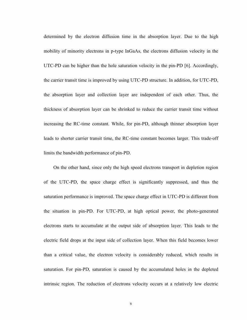
and relatively high responsivity. Band diagram of the pin-PD is schematically shown in
Fig. 1.1 [3]. It consists of a lightly doped intrinsic region, sandwiched between highly
doped n+ and p+ regions. The intrinsic region is much wider than the n+ and p+ regions
to absorb large number of photons and to achieve high quantum efficiency. Electron-hole
pairs are generated in the intrinsic region. At operation bias voltage, the intrinsic region is
entirely depleted, and thus the electric field in this region is high. Then, the generated
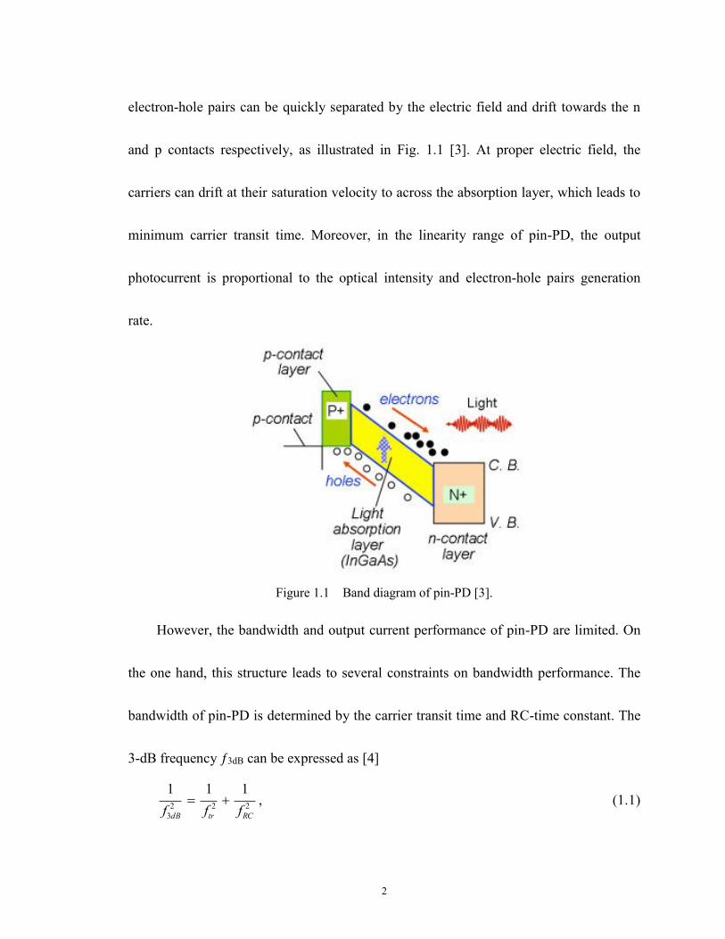
2
electron-hole pairs can be quickly separated by the electric field and drift towards the n
and p contacts respectively, as illustrated in Fig. 1.1 [3]. At proper electric field, the
carriers can drift at their saturation velocity to across the absorption layer, which leads to
minimum carrier transit time. Moreover, in the linearity range of pin-PD, the output
photocurrent is proportional to the optical intensity and electron-hole pairs generation
rate.
Figure 1.1 Band diagram of pin-PD [3].
However, the bandwidth and output current performance of pin-PD are limited. On
the one hand, this structure leads to several constraints on bandwidth performance. The
bandwidth of pin-PD is determined by the carrier transit time and RC-time constant. The
3-dB frequency ƒ3dB can be expressed as [4]
222
3
111
RCtrdB fff , (1.1)

3
in which, ƒtr is the transit time limited bandwidth, ƒRC is the RC-time constant limited
bandwidth. They are given by [4]
d
vftr 2
5.3 ,
444
11
2
11
he vvv, (1.2)
ARR
d
CRf
LSpdtotRC )(22
1
. (1.3)
Here, ν is the average carrier drift velocity of electron velocity νe and hole velocity νh, d
is the intrinsic region thickness, Rtot is the total resistance including series resistance RS
and load resistance RL, and Cpd is the junction capacitance which is related to the
permittivity ε of the depletion region, the active region area A and the intrinsic region
thickness. According to Eq. (1.2), we can see that, for pin-PD, the transit time bandwidth
is mainly limited by the hole velocity, since the hole velocity is much lower than that of
electron. The transit time can be reduced by decreasing the intrinsic region thickness d.
However, according to Eq. (1.3), shorter d results in lower RC-time constant limited
bandwidth. Moreover, the efficiency drops with shorter intrinsic region thickness. On the
other hand, pin-PD is hard to operate at high optical injection level, and thus limiting the
output current. This is mainly due to the space-charge effect [5]. Since electrons drift
faster than holes, under high illumination power, holes accumulate in the depleted
intrinsic region near the i-n interface. The accumulated space charge results in the

4
degradation of the electric field near the n-contact layer side. Thus, as the electric field
decreases, the carrier velocity drops which leads to lower bandwidth and the output
current saturation.
In order to reduce the constraints to improve the bandwidth and saturation
performance, a modified structure, which is referred to UTC-PD, is demonstrated by T.
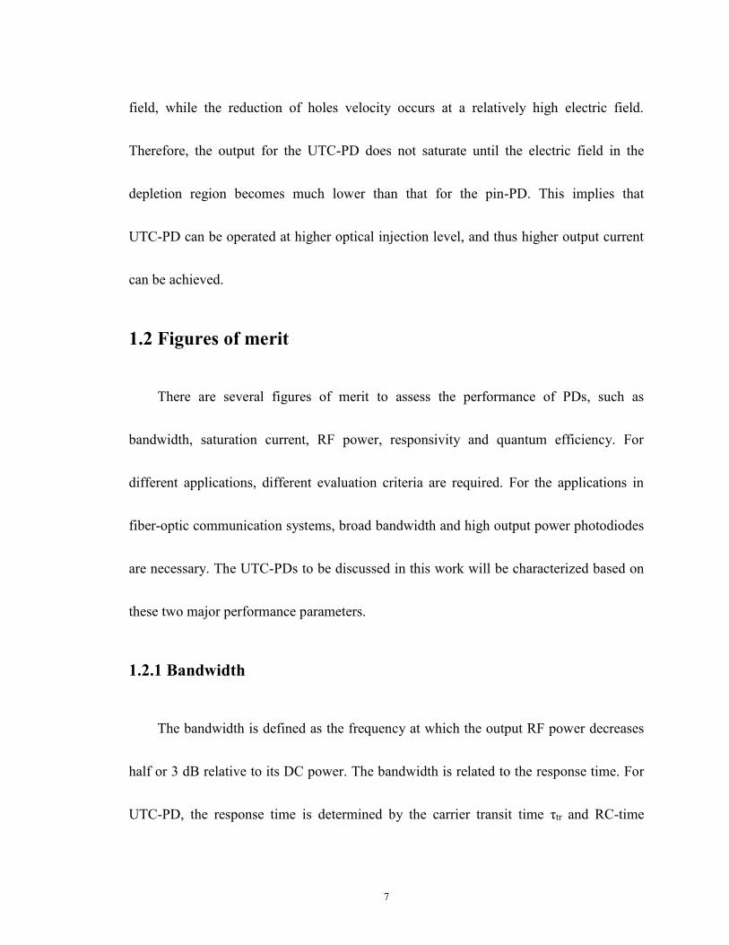
Ishibashi et al. [6]-[9]. The band diagram of the UTC-PD is shown in Fig. 1.2 (a) [3], and
the schematic of its epi-structure is illustrated in Fig. 1.2 (b). Different from the intrinsic
absorption depletion region for the conventional pin-PD, for UTC-PD, the light
absorption region and the depleted collection region are separated. UTC-PD employs a
thicker p-type highly doped narrow bandgap InGaAs layer as the light absorption layer
and utilizes an undoped (or lightly n-type doped) wide bandgap InP layer instead of the
intrinsic layer. Since the energy gap of the InP is larger than the photon energy, it is
transparent to the incident light. Thus, the electron-hole pairs are only generated in the
heavily p-doped InGaAs absorption layer. Moreover, since the holes are the majority
carriers in the absorption layer, the photogenerated holes respond in a very fast dielectric
relaxation time. Therefore, for UTC-PD, the role of holes as the active carriers is
eliminated, and thus only the transportation of the photogenerated high speed electrons
determines the device performance. This is a crucial difference from the conventional
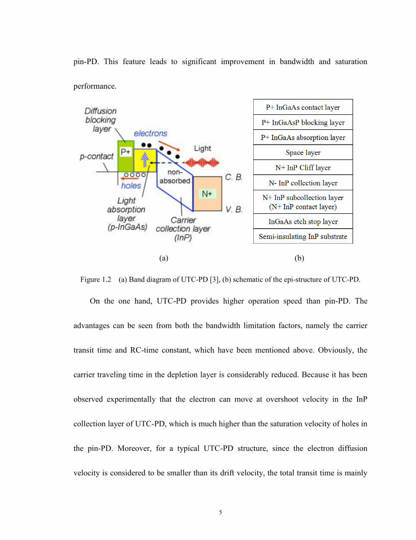
5
pin-PD. This feature leads to significant improvement in bandwidth and saturation
performance.
(a) (b)
Figure 1.2 (a) Band diagram of UTC-PD [3], (b) schematic of the epi-structure of UTC-PD.
On the one hand, UTC-PD provides higher operation speed than pin-PD. The
advantages can be seen from both the bandwidth limitation factors, namely the carrier
transit time and RC-time constant, which have been mentioned above. Obviously, the
carrier traveling time in the depletion layer is considerably reduced. Because it has been
observed experimentally that the electron can move at overshoot velocity in the InP
collection layer of UTC-PD, which is much higher than the saturation velocity of holes in
the pin-PD. Moreover, for a typical UTC-PD structure, since the electron diffusion
velocity is considered to be smaller than its drift velocity, the total transit time is mainly
6
determined by the electron diffusion time in the absorption layer. Due to the high
mobility of minority electrons in p-type InGaAs, the electrons diffusion velocity in the
UTC-PD can be higher than the hole saturation velocity in the pin-PD [6]. Accordingly,
the carrier transit time is improved by using UTC-PD structure. In addition, for UTC-PD,
the absorption layer and collection layer are independent of each other. Thus, the
thickness of absorption layer can be shrinked to reduce the carrier transit time without
increasing the RC-time constant. While, for pin-PD, although thinner absorption layer
leads to shorter carrier transit time, the RC-time constant becomes larger. This trade-off
limits the bandwidth performance of pin-PD.
On the other hand, since only the high speed electrons transport in depletion region
of the UTC-PD, the space charge effect is significantly suppressed, and thus the
saturation performance is improved. The space charge effect in UTC-PD is different from
the situation in pin-PD. For UTC-PD, at high optical power, the photo-generated
electrons starts to accumulate at the output side of absorption layer. This leads to the
electric field drops at the input side of collection layer. When this field becomes lower
than a critical value, the electron velocity is considerably reduced, which results in
saturation. For pin-PD, saturation is caused by the accumulated holes in the depleted
intrinsic region. The reduction of electrons velocity occurs at a relatively low electric
7
field, while the reduction of holes velocity occurs at a relatively high electric field.
Therefore, the output for the UTC-PD does not saturate until the electric field in the
depletion region becomes much lower than that for the pin-PD. This implies that
UTC-PD can be operated at higher optical injection level, and thus higher output current
can be achieved.
1.2 Figures of merit
There are several figures of merit to assess the performance of PDs, such as
bandwidth, saturation current, RF power, responsivity and quantum efficiency. For
different applications, different evaluation criteria are required. For the applications in
fiber-optic communication systems, broad bandwidth and high output power photodiodes
are necessary. The UTC-PDs to be discussed in this work will be characterized based on
these two major performance parameters.
1.2.1 Bandwidth
The bandwidth is defined as the frequency at which the output RF power decreases
half or 3 dB relative to its DC power. The bandwidth is related to the response time. For
UTC-PD, the response time is determined by the carrier transit time τtr and RC-time

8
constant τRC. Then, the 3-dB bandwidth ƒ3dB can be approximately expressed as Eq. (1.4).
In order to improve the bandwidth performance, both τtr and τRC should be decreased.
223
2
1
RCtr
dBf
. (1.4)
For a typical UTC-PD, the carrier transit time τtr includes the carrier diffusion time
τA in the low electric field absorption layer, and the carrier drift time τC in the high
electric field depleted collection layer. The diffusion time τA can be given by [6]
th
A
e
AA
v
W
D
W
3
2
, (1.5)
where WA is the absorption layer thickness, De is the diffusion coefficient of electrons in
the absorption layer and νth is the electron thermionic emission velocity. The drift time
can be expressed as [6]
os
CC
v
W , (1.6)
where WC is the collection layer thickness and νos is the overshoot velocity of the
electrons. The carrier transit time can be reduced by reducing the thickness of absorption
and collection layers. Additionally, a built-in electric field can be constructed in the
absorption layer to accelerate the electrons, and thus shorten the transit time. When the
thickness of absorption layer is similar to that of the collection layer, the carrier transit
time τtr is primarily limited by the carrier traveling time τA in absorption layer, since the
9
electron diffusion velocity is much slower than the electron drift velocity. Thus, τtr can be
approximated as follows,
th
A
e
AACAtr
v
W
D
W
3
2
. (1.7)
On the other hand, the RC-time constant τRC can be expressed as [10]
W
ARRCR LSpdtotRC
)( , (1.8)
where Rtot is the total resistance including series resistance RS and load resistance RL. Cpd
is the junction capacitance, which is determined by the thickness W of depletion region
and the area A of the active region. And ε is the permittivity of the depletion region. The
RC-time constant τRC can be minimized by decreasing the area of active region or
increasing the thickness of depletion region. However, the contact resistance is inversely
proportional to the contact area, and a thicker depletion region leads to a longer transit
time, therefore trade-offs exist in these aspects.
The 3-dB frequency ƒ3dB can be extracted by using two different methods. The first
method is to obtain the 3-dB frequency from the Fourier transform of the pulse response.
The other method is that, the bandwidth of the device can be evaluated from the
frequency response to a modulated optical signal. In this work, the second method is used
to analyze the bandwidth performance.
10
1.2.2 Output RF power
The output RF power of the UTC-PD refers to the power delivered to load resistance,
which can be expressed as follows [9][10],
])2(1][)2(1[2)(
22
22
RCtr
opL
RFff
MLPrRfP
. (1.9)
Here, ƒ is the frequency, RL is the load resistance, r is responsivity, Pop is the input optical
power, M is a factor related to the optical modulation index, and L is a factor related to
optical and electrical losses. Due to the development of the optical fiber amplifier, it is
desired to place the the optical fiber amplifier directly in front of the photodiode to
eliminate the costly post-amplifier. This is because, as the frequency increases, a
photoreceiver consisting of an optical pre-amplifier and a high-power photodiode can
produce better characteristics than a conventional photoreceiver with electrical
post-amplifiers, and the system configuration can be simplified as well [6]. Thereby,
high-speed and high-output power photodiodes with high-power handling capability are
required.
According to Eq. (1.9), the output power decreases as the frequency increases, since
the carrier transit time and RC-time constant limitations become significant. On the other
hand, the output power rises with increasing input optical power. However, as the input
11
optical power grows, the space-charge effect becomes significant. Due to the space
charge, the electric field in the front part of depletion region drops, and thus the carrier
velocity is reduced, which in turn causes the degradation of bandwidth and output power.
The output power saturation occurs when the input optical power is high enough. At high
optical injection level, owing to the space-charge effect, the high-speed performance of
UTC-PD is limited, which results in the output power decreases more rapidly with
increasing frequency. The space-charge effect can be weakened by increasing the reverse
bias voltage. However, this may cause the thermal failure.
In this work, the output RF power performance is evaluated from the DC
photocurrent response to the optical source. This is because, the current is related to the
output power, and they are closely affected by the space-charge effect. Both of them
increase linearly with the incident optical power, and then deviate from the linear
response, which effectively indicates the saturation occurs.
1.3 Motivation of this research
1.3.1 Literature review
In the past decade, there has been an increasing interest in UTC-PD due to its
excellent speed and saturation current performance. Various improvements, in terms of

12
layer structure, optical coupling and packaging, have been achieved. As the UTC-PD
reported in [11], the most straightforward way to enhance the speed performance is to
scale down the thickness of absorption layer. However, thin absorption layer seriously
reduces the responsivity of the device. It has been experimentally demonstrated that the
bandwidth performance of UTC-PD can be improved by incorporating a step-like doping
profile in the photoabsorption layer, since the introduced built-in electric field can help
electrons transport more rapidly into the collector [12]. The modified UTC-PD
(MUTC-PD) structures, which employ partially depleted absorption layer to improve the
bandwidth and the quantum efficiency, have been achieved [13]-[15]. Besides, the
saturation current performance of the MUTC-PD can be enhanced by inserting a cliff
layer before the collector [16]. A non-uniformly doped collector was designed to relax
the space-charge effect, and thus the saturation current can be enhanced [17]. Superior
bandwidth and output power performance of Near-ballistic UTC-PD (NBUTC-PD) has
been demonstrated [18]-[19]. Moreover, different methods of optical coupling have been
developed [20]-[23]. For instance, an edge-coupled waveguide UTC-PD was
demonstrated to show improved performance [24]. Additionally, in terms of fabrication
process improvements, well-designed packaging techniques, which are used to
effectively manage the heat sinking problem, have been implemented [25]-[27]. By
13
flip-chip bonding the UTC-PDs on submounts with high thermal conductivity, the power
handling capability of PDs can be increased, and thus the high-power performance is
greatly improved [28].
1.3.2 Motivation
In this thesis, in order to improve the bandwidth and saturation performance of
UTC-PD, we developed novel absorption layer and collection layer structures. And the
effects of these structures are investigated by using a numerical device simulator.
1.4 Thesis organisation
The rest of the thesis is organized as follows.
Chapter 2 describes the device structure and the physics-based modeling of the
considered UTC-PD. It is noted that hot carrier transport equations are enabled in our
simulation. The simulation results are compared with the reported results to ensure the
accuracy of the physical modeling. Then, in the following chapters, the UTC-PDs are
investigated and designed by using physics-based modeling.
In chapter 3, the bandwidth performance of the considered UTC-PD is investigated
and enhanced. First of all, the effect of widely used linearly graded doping absorption

14
layer is studied. Then, the function of graded bandgap absorption layer is investigated.
Moreover, both the methods are optimized by using partially graded structure. Finally,
the benefits of proposed combined graded absorption layer are presented.
In chapter 4, the saturation performance of the considered UTC-PD is investigated
and improved. Firstly, the space-charge effect and charge compensation effect is studied.
Then, a collection layer with linear doping profile is proposed and optimized, a better
saturation performance is predicted. Furthermore, a Gaussian doping profile is proposed,
which can further improve the saturation performance.
Chapter 5 presents two the epitaxial layer structures of designed UTC-PDs. Their
bandwidth and saturation performance is simulated. Additionally, the major steps of the
fabrication process are described.
Chapter 6 presents the conclusions and suggestions for future work.
15
Chapter 2 Physics-Based UTC-PD Modeling
The performance of the UTC-PD can be predicted by using the physics-based
modeling. One of the advantages of the physics-based simulation method is that, the
device can be studied in detail without costly experiments. Appropriate physical models
must be incorporated to ensure the accuracy of the modeling. The drift-diffusion model is
widely used to describe the carrier transport. However, the drift-diffusion approximation
becomes less accurate in the simulation of submicron devices. The non-local effects, such
as velocity overshoot, which has been observed experimentally in UTC-PDs [29], is not
considered in this model. Therefore, in this work, a more appropriate energy balance
transport model is employed in the device modeling. Then, different device structures are
studied and designed based on the simulation results, which are obtained by solving hot
carrier transport equations.
A commercial physics-based device simulator ATLAS, by Silvaco International, is
used in this work. ATLAS provides general capabilities for physics-based two (2D) and
three-dimensional (3D) simulation of semiconductor devices [30]. It contains a
comprehensive set of physical models, including drift-diffusion transport models, energy
balance and hydrodynamic transport models, concentration, electric field and temperature

16
dependent mobility models, carrier generation and recombination models, etc. And it
employs powerful numerical techniques, such as Gummel, Newton, and block-Newton
nonlinear iteration strategies. In ATLAS, semiconductor device can be modeled by a set
of coupled and non-linear partial differential equations, which are derived from
Maxwell’s laws [30]. After defining a fine meshed physical structure and setting
reasonable parameters, by using the provided numerical methods, numerical solutions of
these equations can be obtained on every grid points within the device structure. Based
on these results, the electric field can be obtained at any position within the device, and
the diffusion and drift current, as well as terminal current and voltage, can be calculated.
Furthermore, the performance of the device can be achieved in DC, AC small signal or
transient modes of operation under different bias conditions. Thus, the transport
phenomena within the device can be analyzed and the characteristics can be predicted as
well.
In this chapter, we first describe the basic device structure which will be considered
in this chapter and next two chapters. Subsequently, we present some important material
properties and physical models which are employed for device simulation. Moreover,
several important equations which are solved inside the simulator are introduced. Finally,
17
in order to verify the accuracy of our physical modeling, we compared the simulation
results with the experimental results in [6] and the simulated results in [31].
2.1 Device structure
In this and next chapter, we will consider a basic UTC-PD device structure which is
reported by T. Ishibashi et al. [6]. The epitaxial layers are shown in Table 2.1. In addition
to the absorption layer and the collection layer, the other layers are used as electrical
contact layers or are added for improving performance. The topmost layer is the p-type
InGaAs contact layer, which contacts with the anode metal. In order to form a good
ohmic contact, this layer is heavily doped. It is followed by a wide bandgap p-type
InGaAsP blocking layer which is lattice matched to InP. Since the energy gap of the
blocking layer is 0.85 eV, and the energy gap of the following p-type InGaAs absorption
layer is 0.737 eV, a conduction band offset ΔEc is formed at the blocking layer and
absorption layer interface, which serves as a diffusion barrier for the electrons in the
absorption layer. Thus, the role of the blocking layer is to promote the electrons
generated in the absorption layer to move towards the InP collection layer and to prevent
the diffusion of the electrons to the anode, while allowing the holes pass through.
Followed is a typical uniformly doped p-type InGaAs layer that is used as the absorption
18
layer. It is highly doped to 1x1018 cm-3 and the thickness is 220 nm. Corresponding to the
optical wavelength of 1.55 μm, which is equivalent to photon energy of 0.8 eV, the
energy gap of this absorption layer is designed to be 0.737 eV to ensure the electrons can
be excited from the valence band to the conduction band. Relatively, in order to avoid
optical absorption, a n-type InP layer which has a wide energy gap of 1.35 eV is adopted
as the collection layer. It is uniformly doped to 1x1016 cm-3 for charge compensation.
Moreover, the doping concentration is very low to ensure this region can be completely
depleted at normal device operation bias. Since there is an abrupt conduction band barrier
at the InGaAs and InP heterojunction interface, which may block the electrons and lead
to degradation of the sensitivity and photocurrent, undoped InGaAs, InGaAsP and InP
space layers are employed to form a smooth connection between the absorption layer and
collection layer. The energy gap of the inserted InGaAsP space layer is 1.0 eV.
Additionally, a n-type thin InP cliff layer is added between the undoped InP spacer layer
and the lightly doped InP collection layer. This cliff layer, which is highly doped to
1x1018 cm-3, is used to enhance the electric field in the depleted region near the
absorption layer and collection layer interface. Finally, similar to the p-type contact layer,
the cathode metal is connected to the n-type InP subcollection layer, which is heavily
doped to reduce the contact resistance.

19
Table 2.1 Epitaxial layers of the UTC-PD reported in [6].
Layer Thickness (nm) Doping (cm-3)/Type Band gap Eg (eV)
p++InGaAs contact 50 3×10¹⁹/P 0.737
p++InGaAsP blocking 20 2×10¹⁹/P 0.85
p+ InGaAs absorption 220 1×10¹⁸/P 0.737
i-InGaAs space 8 -- 0.737
i-InGaAsP space 16 -- 1.0
i-InP space 6 -- 1.35
n+ InP cliff 7 1×10¹⁸/N 1.35
n- InP collection 263 1×10¹⁶/N 1.35
n+ InP subcollection-2 50 5×10¹⁸/N 1.35
n+ InGaAs etch stop 10 1.5×10¹⁹/N 0.737
n+ InP subcolleciton-1 500 1.5×10¹⁹/N 1.35
i-InGaAs etch stop 10 -- 0.737
(S. I. InP Sub)
2.2 Definition of material parameters and models
In order to simulate the UTC-PD as described above, the following basic steps are
performed in ATLAS. First of all, we need to define the device structure as listed in
Table 2.1, for example, specifying regions and electrodes, as well as the doping profiles.
Secondly, we should specify the mesh of structure, which generates a suitable grid to
ensure the accuracy of the simulation. Once we define the device structure and the mesh,
we can set the material parameters. For commonly used conventional materials, such as
InP, we adopt the default parameters contained in the simulator. For unusual materials,
the essential parameters are obtained from the reported literatures and website [32]. Then,
20
we need to specify reasonable physical models. Subsequently, the optical source should
be defined. After these steps, we choose suitable numerical methods to calculate the
solutions to the specified device problems. Finally, DC, AC small signal and transient
simulations can be obtained at different bias, light intensity and frequency conditions as
we specified. In the following sections, we present some important parameters that need
to be defined in ATLAS. For instance, the composition fractions x and y of
In1-xGaxAsyP1-y which have a marked impact on the energy bandgap and band offsets
distribution, as well as the optical parameters which we obtained from the reported
literature and employed in ATLAS. Moreover, the physical models, which we used for
UTC-PD simulation, are described.
2.2.1 Energy gaps and heterojunction band offsets setting
As mentioned above, for the UTC-PD reported by T. Ishibashi et al. [6], there are
two different layers constituted by a quaternary material InGaAsP. One of them is the
InGaAsP blocking layer, which is used to promote the electrons generated in the
absorption layer move towards the InP collection layer and to prevent the diffusion of the
electrons to the anode, while allowing the holes pass through. The other one is the
InGaAsP space layer which is inserted between the absorption layer and collection layer

21
and acts as a intermediate layer to flatten the conduction band barrier and facilitate
electrons to transport into the InP collection layer. The functions of these two different
layers are realized by specifying different energy gaps. And the energy bandgap of the
In1-xGaxAsyP1-y quaternary material is determined by its composition fractions x and y.
Thus, the setting of values of the composition fractions is very important when we
initially define the device structure.
The default energy gap for the InP lattice matched In1-xGaxAsyP1-y system used in
the simulator is given by [30]
xyyx
yyxxEg
)159.0109.028.0(
)101.1101.0()758.0642.0(35.1)PAsGaIn( y1yxx-1
. (2.1)
Since this In1-xGaxAsyP1-y material must be lattice matched to InP, the relationship
between x and y that satisfy this condition is given by [33]
y
yx
0125.04176.0
1896.0
. (2.2)
According to these two equations, we can obtain the values of the composition fractions
for the In1-xGaxAsyP1-y layers which are employed in the considered UTC-PD. For the
blocking layer which is designed to have an energy gap of 0.85 eV, the corresponding
values of composition fractions are calculated as x=0.351, y=0.755. For the space layer
which has an energy gap of 1.0 eV, the composition fractions are given by x=0.230,
y=0.499.
22
Once we set the composition fractions for every layer in the UTC-PD, the energy
gap of each layer is determined. Then, the conduction and valence band discontinuities
are formed by the difference between the energy gaps of two adjacent materials. Since
the distribution of energy gap between the conduction and valence bands has a large
impact on the charge transport, it is very important to properly define the conduction
band offset ΔEc and the valence band offset ΔEv at each heterojunction interface. Thereby,
the energy gap of each layer should be properly aligned [34]. In the simulator, one of the
methods that defines the conduction band alignment for a heterointerface is to manually
adjust the material affinities by specifying the AFFINITY parameter in the MATERIAL
statement. The procedure for aligning heterojunctions using this method is described as
follows.
First of all, the electron affinity of In0.53Ga0.47As is set to 4.58 eV [33]. For the
In1-xGaxAsyP1-y and In0.53Ga0.47As heterojunction system that is lattice matched to InP, the
conduction band offset ΔEc and the valence band offset ΔEv can be expressed
mathematically in terms of the composition of the quaternary as follows [33],
2003.0268.0271.0)( yyyEc , (2.3)
2152.0502.035.0)( yyyEv . (2.4)
23
Accordingly, at the above described In0.649Ga0.351As0.755P0.245 blocking layer and
In0.53Ga0.47As absorption layer heterojunction interface, we can obtain that ΔEc=0.07 eV
and ΔEv=0.058 eV. Then, the electron affinity of the In0.649Ga0.351As0.755P0.245 blocking
layer can be derived from the conduction band offsets ΔEc and the specified electron
affinity of In0.53Ga0.47As. Accordingly, the electron affinity of the wide energy gap
blocking layer is adjusted to 4.58-0.07=4.51 eV to ensure the desired conduction band
offset at the heterojunction interface. Similarly, at the In0.53Ga0.47As and
In0.77Ga0.23As0.499P0.501 space layer heterojunction interface, the corresponding conduction
band offset ΔEc is 0.138 eV and the valence band offset ΔEv is 0.137 eV. Thereby, the
electron affinity of the In0.77Ga0.23As0.499P0.501 space layer should be modified to
4.58-0.138=4.442 eV. Subsequently, for the following lattice matched In1-xGaxAsyP1-y
and InP heterojunction system, the equations to calculate the band offsets are given by
[33]
2003.0268.0 yyEc , (2.5)
2152.0502.0 yyEv . (2.6)
According to the above equations, the band offsets at the In0.77Ga0.23As0.499P0.501 and InP
space layer interface can be calculated as ΔEc=0.134 eV and ΔEv=0.213 eV respectively.
Therefore, we need to set the AFFINITY parameter of InP to 4.442-0.134=4.308 eV.
24
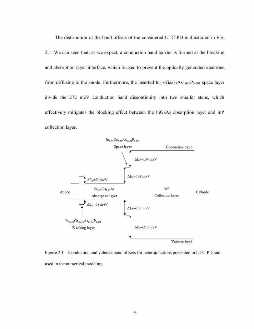
The distribution of the band offsets of the considered UTC-PD is illustrated in Fig.
2.1. We can seen that, as we expect, a conduction band barrier is formed at the blocking
and absorption layer interface, which is used to prevent the optically generated electrons
from diffusing to the anode. Furthermore, the inserted In0.77Ga0.23As0.499P0.501 space layer
divide the 272 meV conduction band discontinuity into two smaller steps, which
effectively mitigates the blocking effect between the InGaAs absorption layer and InP
collection layer.
Figure 2.1 Conduction and valence band offsets for heterojunctions presented in UTC-PD and
used in the numerical modeling.

25
2.2.2 Defining optical properties of materials
Since UTC-PD is an optoelectronic device, the optical properties of the materials are
crucial for device simulation. One of the most important optical parameters is the
complex index of refraction inn ~ . Here, the real part of the refractive index n
indicates the phase velocity, while the imaginary part κ indicates the amount of
absorption loss when the electromagnetic wave propagates through the material [35]. In
the absorption layer of UTC-PD, the incident light intensity at a distance z into the
absorption layer decays exponentially from the surface. It can be expressed as
)exp()( 0 zPyP , (2.7)
where P0 is the intensity of the incident radiation and α is the absorption coefficient. Then,
based on this expression, the generation rate formula can be derived. In ATLAS, the
generation rate formula is given by [30]
)exp(0 zc
PG
, (2.8)
where P is the ray intensity factor, which contains the cumulative effects of reflections,
transmissions, and loss due to absorption over the ray path, η0 is the internal quantum
efficiency, z is a relative distance for the ray, ħ is Planck’s constant, c is the speed of light,
λ is the wavelength and α is the absorption coefficient. The generation associated with
26
each grid point can be calculated by integration of the generation rate formula. In
addition, for ATLAS, the absorption coefficient α is obtained from the imaginary part κ
of the complex index of refraction, according to the following Eq. (2.9) [30],
4 . (2.9)
Hence, absorption or photogeneration is related to the imaginary component of refractive
index. On the other hand, for the simulator, optical ray tracing model uses the real
component of refractive index to calculate the optical intensity at each grid point [30].
Therefore, taking all these descriptions, we must carefully specify the complex index of
refraction of the specific regions in the device structure.
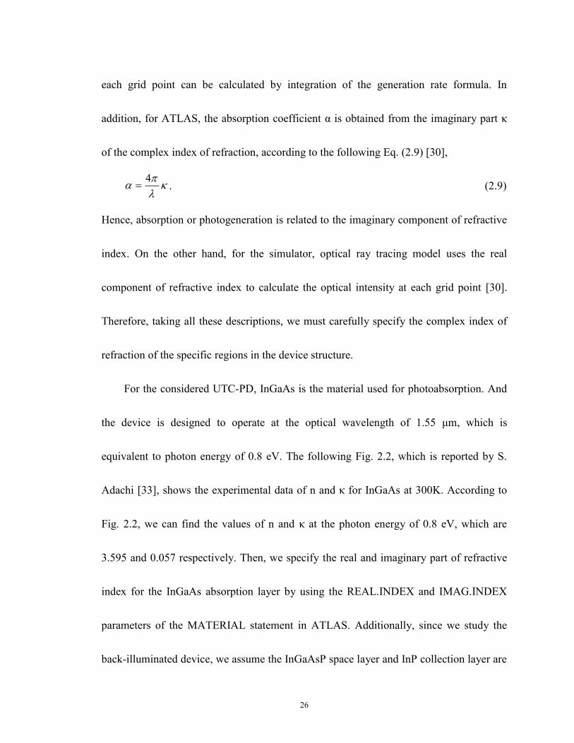
For the considered UTC-PD, InGaAs is the material used for photoabsorption. And
the device is designed to operate at the optical wavelength of 1.55 μm, which is
equivalent to photon energy of 0.8 eV. The following Fig. 2.2, which is reported by S.
Adachi [33], shows the experimental data of n and κ for InGaAs at 300K. According to
Fig. 2.2, we can find the values of n and κ at the photon energy of 0.8 eV, which are
3.595 and 0.057 respectively. Then, we specify the real and imaginary part of refractive
index for the InGaAs absorption layer by using the REAL.INDEX and IMAG.INDEX
parameters of the MATERIAL statement in ATLAS. Additionally, since we study the
back-illuminated device, we assume the InGaAsP space layer and InP collection layer are
27
transparent at the optical wavelength of 1.55 μm. Thereby, for these transparent layers,
we set the imaginary part κ of refractive index to zero. For InP, the real part of refractive
index n is specified as 3.165 [36]. And for In1-xGaxAsyP1-y, we can define its real part of
refractive index according to the relation n=3.1+0.46y [37].
Figure 2.2 Real and imaginary parts of the refractive index for InGaAs versus
photon energy [33].
2.2.3 The energy balance transport model
The conventional drift-diffusion model is the simplest charge transport model. It is
useful for most of the common devices. However, as the sizes of the devices become
smaller, this drift-diffusion approximation is less accurate, since it neglects non-local
effects such as velocity overshoot, diffusion associated with the carrier temperature and
the dependence of impact ionization rates on carrier energy distributions. These non-local
28
effects are considered very important in the simulation of submicron devices. In addition,
electron velocity overshoot has been observed experimentally in UTC-PDs [29]. The
electron velocity plays a significant role in determining the performance of UTC-PD.
Therefore, in order to ensure the accuracy of the simulation for the studied UTC-PD, the
non-local model of charge transport is required.
In ATLAS, these effects can be modeled by using the energy balance transport
model. The energy balance transport model follows the derivation by Stratton [38]-[39],
which is derived starting from the Boltzmann transport equation. The energy balance
equations are given by [30]
)(2
31*
nnnnn nTt
kWEJ
qS
, (2.10)
)(2
31*
ppppp pTt
kWEJ
qS
, (2.11)
in which Jn and Jp are the current densities, Sn and Sp are the energy flux densities from
the carrier to the lattice. They can be expressed as [30]
n
T
nnnn TqnDnqnqDJ , (2.12)
p
T
pppp TqpDpqpqDJ , (2.13)
nnn
nnn TJq
kTKS
, (2.14)
pp
p
ppp TJq
kTKS
. (2.15)

29
Here, Tn and Tp are the temperature of electrons and holes, Wn and Wp are the energy
density loss rates for electrons and holes, Dn and Dp are the thermal diffusivities for
electrons and holes, and Kn and Kp are the thermal conductivities of electrons and holes.
For our simulation, in order to take into account the electron velocity overshoot effect, we
specified HCTE.EL parameter in the MODELS statement to activate the hot carrier
transport equations for electrons only.
2.2.4 Mobility models
Carrier mobilities are the functions of the doping concentration, local electric field,
lattice temperature, and so on. The simulator ATLAS provides several models to account
for these effects. For the studied UTC-PD, we need to consider carriers mobilities in
low-field behavior and high-field behavior. Suitable mobility models are employed for
the simulation. They will be presented as follows.
2.2.4.1 Concentration dependent mobility model
For the low-field condition, the carrier mobility is affected by impurity scattering.
The mobilities of holes and electrons decrease with increasing doping concentration.
30
Thus, the CONMOB model is employed. It provides empirical data for the doping
dependent low-field mobilities of electrons and holes [30].
2.2.4.2 Parallel electric field dependent mobility model
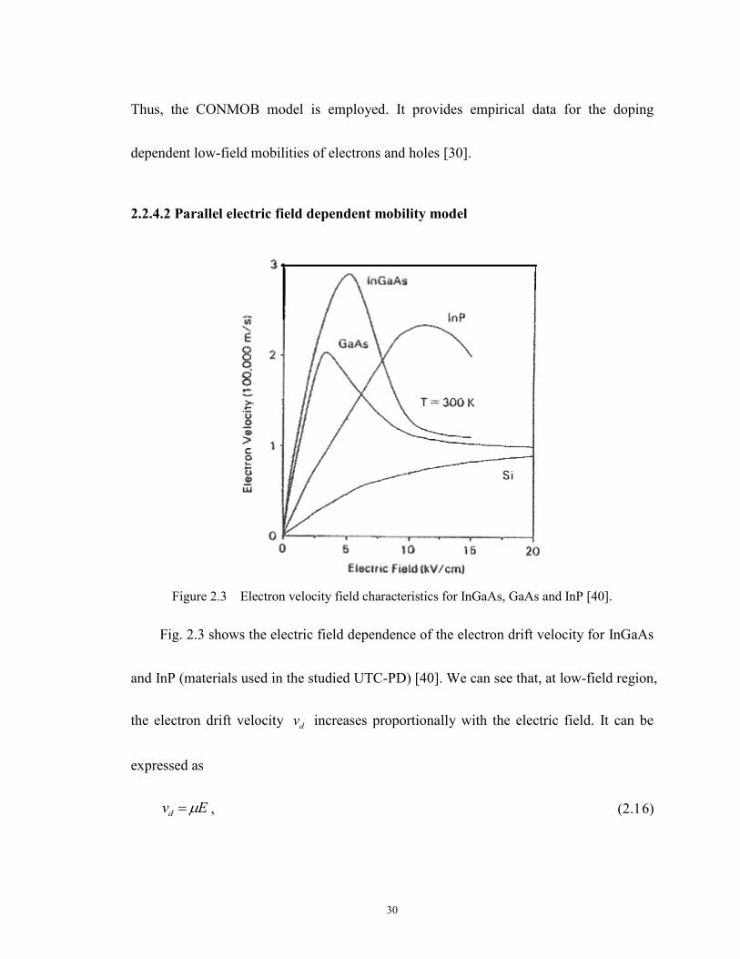
Figure 2.3 Electron velocity field characteristics for InGaAs, GaAs and InP [40].
Fig. 2.3 shows the electric field dependence of the electron drift velocity for InGaAs
and InP (materials used in the studied UTC-PD) [40]. We can see that, at low-field region,
the electron drift velocity dv increases proportionally with the electric field. It can be
expressed as
Evd , (2.16)
31
where E is the electric field, µ is the carrier mobility. While, at high electric field, drift
velocity no longer increases linearly with increasing electric field, and eventually, it tends
to saturation. This is because the carrier energy obtained from electric field is transferred
to lattice during the scattering processes. Since the magnitude of the drift velocity is the
product of the mobility and the electric field, at high electric field, the effective mobility
need to be reduced. In ATLAS, this field dependent mobility can be modeled by using
parallel electric field mobility model FLDMOB. This model employ the following
Caughey and Thomas expression [41] (Eq. (2.17) and Eq. (2.18)) to implement a field
dependent mobility. Thereby, a smooth transition between low-field and high-field
behavior is achieved.
n
n
satn
n
v
Enn E
1
1
10
0
. (2.17)
p
p
satp
p
v
Epp E
1
1
10
0
. (2.18)
Here, µn0 and µp0 are the low-field electron and hole mobilities respectively, vsatn and vsatp
are the saturation velocities of electron and hole respectively and βn and βp are
user-definable parameters, which we use their defaults, i.e. βn=2 and βp=1. The low-field
32
mobilities µn0 and µp0 are obtained from the previously described low-field mobility
model.
2.2.4.3 Energy dependent mobility model
For the employed energy balance transport model, the carrier mobility is required to
be related to the carrier energy. This can be achieved through the homogeneous steady
state energy balance relationship. The effective electric fields, Eeff,n and Eeff,p, need to be
calculated, according to the following equations derived from the energy balance
equations [30].
nmob
Lnneffneffn
TTkEEq
,
2
,,
)(
2
3)(
, (2.19)
pmob
Lp
peffpeffp
TTkEEq
,
2
,,
)(
2
3)(
. (2.20)
Here, TL is the lattice temperature, k is Boltzmann’s constant and τmob,n and τmob,p are
user-definable parameters, which we use their defaults, τmob,n=τmob,p=2.5x10⁻¹³ s. Then,
these effective electric fields are introduced into the relevant field dependent mobility
model.
In the above mentioned FLDMOB model, the carrier mobility is not dependent on
temperature. While, in energy balance transport model, the carrier mobility is treated as
function of the carrier temperature rather than function of the local electric field. Thus,
33
the standard saturation model is chosen by setting EVSATMOD=0 on the MODELS
statement. In this model, the carrier mobility, which depends on the carrier temperature,
can be expressed as follows [30],
nn
n
nn
X
1
0
)1(
, (2.21)
pp
p
p
p
X
1
0
)1(
, (2.22)
in which,
))(4)()((2
1 22 nnnnnnn
LnnLnnLnnn TTTTTTX , (2.23)
))(4)()((2
1 22 ppppppp
LppLppLppp TTTTTTX
, (2.24)
nelsatn
nBn
qv
k
,
2
0
2
3
, (2.25)
pelsatp
pB
pqv
k
,
2
0
2
3
. (2.26)
Here, τel,n and τel,p are the energy relaxation times for electrons and holes.
2.2.5 Recombination models
For the studied UTC-PD, in order to return to equilibrium after the generation of
electron-hole pairs, the carrier recombination occurs in the device. According to the form
of the lost energy of electron, the generation-recombination mechanisms can be divided
34
into several types, such as phonon transitions and Auger transitions. Thus, in ATLAS, we
need to specify the suitable models to simulate these processes.
2.2.5.1 Shockley-Read-Hall (SRH) concentration dependent lifetime model
One of the generation-recombination process that we considered is phonon
transitions. Phonon transitions occur in the presence of a trap or defect within the
forbidden gap of the semiconductor [30]. This is a two step process. An carrier is trapped
by an energy state in the forbidden region, recombination occurs when another carrier of
the opposite conductivity type interacts with the same energy state. This process is called
Shockley-Read-Hall (SRH) recombination. Moreover, the carrier lifetime is an important
parameter in the modeled SRH recombination equations. The carrier lifetime depends on
the impurity concentration. It decreases as the impurity concentration increases. Thereby,
in the simulator, we modeled this recombination process by using SRH concentration
dependent lifetime model CONSRH. By using this model, the net
generation-recombination rate is given as [30]
)]exp([)]exp([
2
LL kTETRAP
iepkTETRAP
ien
ieSRH
nnnp
npnR
, (2.27)
in which,
35
)(1
0
NSRHNN
nn
, (2.28)
)(1
0
NSRHPN
p
p
. (2.29)
Here, ETRAP is the difference between the trap energy level and the intrinsic Fermi level,
τn0 and τp0 are the user-definable electron and hole lifetimes, N is the total impurity
concentration and NSRHN and NSRHP are user-definable parameters.
For the studied UTC-PD, the p-type InGaAs absorption layer is very important. In
order to ensure the accuracy of the simulation, the carrier lifetime in p-type InGaAs need
to be specified according to the the literature as follows. First of all, for p-type material
under low injection condition, the recombination rate Eq. (2.27) can be reduced to
n
SRH
nnR
0
, (2.30)
where n is the total minority electron concentration, n0 is the thermal equilibrium electron
concentration and τn is the minority carrier electron lifetime. Thus, we only need to
consider the minority carrier electron lifetime in p-type InGaAs absorption layer. Then,
according to the experimental data reported by Tashima et al. [42], it is found that the
electron lifetime in p-type InGaAs is a function of the doping level. The electron lifetime
decreases as the doping concentration increases. Furthermore, Conklin et al. [43]
proposed an exponential empirical model to fit the experimental data. This empirical
model can be written as [43]
36
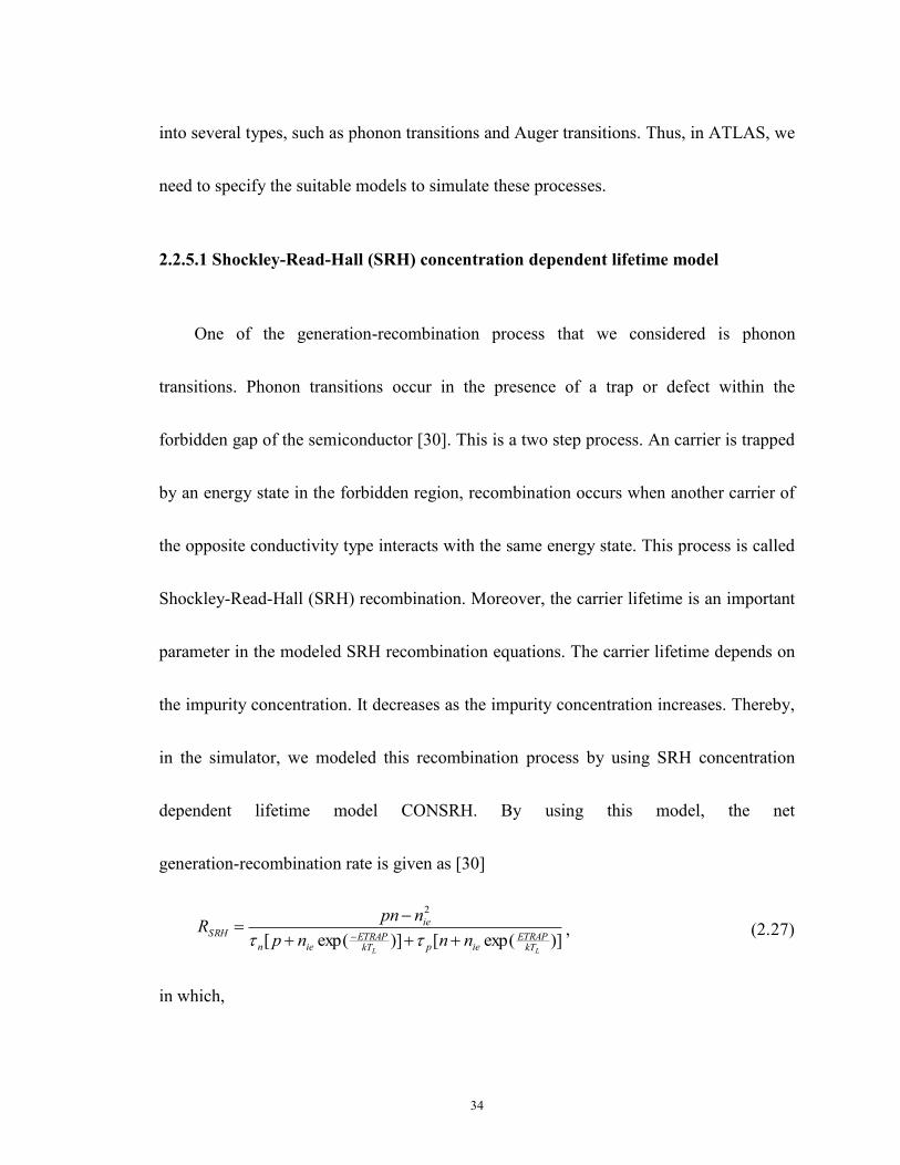
AN
n nlog
10sec)(
, (2.31)
where NA is the base doping concentration and the fit parameters are β=12.6, γ=0.73 for
NA>8x1017 cm-3. For the doping concentration smaller than 8x1017 cm-3, a constant
lifetime of 0.3 ns was assumed. Subsequently, we need to fit the concentration dependent
lifetime model, which is employed in ATLAS, to the data of this empirical model. For the
studied UTC-PD, the p-type InGaAs absorption layer is highly doped to 1x1018 cm-3.
Thus, for the empirical model, we consider the case of NA>8x1017 cm-3. Thereby, the
corresponding parameters used in the CONSRH model can be specified as τn0=0.7 ns and
NSRHN=7.134x1017 cm-3. The fitting result is shown in Fig. 2.4.
1018
1019
1020
0.00
0.05
0.10
0.15
0.20
0.25
0.30
Ele
ctr
on
life
tim
e (
ns)
Doping concentration (cm-3)
Conklin empirical model
CONSRH fitting model
Figure 2.4 Electron lifetime in p-type InGaAs as a function of doping concentration. The solid
line is calculated by using Conklin’s empirical model [43]. The dashed line is the fitting result of
CONSRH model.
37
2.2.5.2 Standard Auger model
The SHR recombination is dominant under conditions of low carrier concentration
or low level injection. However, at high carrier concentration or high level injection,
electrons and holes are more likely to directly interact, which leads to Auger
recombination. Therefore, Auger transitions need to be considered. Auger recombination
occurs through a three particle transition whereby a mobile carrier is either captured or
emitted [30]. The excess energy given off by this recombination process is absorbed by
another carrier. In ATLAS, the standard Auger model AUGER is employed to model this
process as follows [44],
)()( 2222
ieieAuger pnnpAUGPnnpnAUGNR , (2.32)
where the model parameters AUGN and AUGP are user-definable Auger coefficients.
We specified these parameters according to the website [32].
2.3 Basic equations
Semiconductor device operation is modeled in ATLAS by a set of anywhere from
one to six coupled, non-linear, partial differential equations [30]. For different models,
we can obtain the solution of the corresponding equations by using the powerful
numerical methods. In the following, several fundamental equations, which are solved

38
inside the simulator, are described, for instance, Poisson’s equation, the continuity
equations and the transport equations. Poisson’s equation relates variations in
electrostatic potential to local charge densities. The continuity and the transport equations
describe the way that the electron and hole densities evolve as a result of transport
processes, generation processes, and recombination processes [30].
2.3.1 Poisson’s equation
Poisson’s equation is given by [30]
)(div , (2.33)
where ψ is the electrostatic potential, ε is the local permittivity and ρ is the local space
charge density. For ATLAS, the intrinsic Fermi potential is defined as the reference
potential. The local space charge density takes into account all the mobile and fixed
charge. Moreover, the electric field E can be obtained from the gradient of the potential
[30], by using Eq. (2.34).
E . (2.34)
Thereby, Poisson's equation relates local space charge density to electric field.

39
2.3.2 Carrier continuity equations
The carrier continuity equations consider the impact of the various mechanisms on
the carrier concentration. They describe how the carrier concentration varies with time
and space. The continuity equations for electrons and holes are defined as [30]
nnn RGJqt
n
1, (2.35)
ppp RGJqt
p
1, (2.36)
where n and p are the electron and hole concentration, Jn and Jp are the electron and hole
current densities, Gn and Gp are the generation rates for electrons and holes, Rn and Rp are
the recombination rates for electrons and holes, and q is the magnitude of the charge on
an electron.
2.3.3 The transport equations
The charge transport models, or the current density equations, are usually obtained
by applying approximations and simplifications to the Boltzmann transport equation [30].
For the simulation of the submicron UTC-PD in this work, the energy balance transport
model is employed. It uses a higher order approximation to the Boltzmann transport
equation. Compared with conventional drift-diffusion model, it introduces new
independent variables for electron and hole temperatures, adds continuity equations for
40
the carrier temperatures, and treats the carrier mobilities as functions of the carrier
temperatures rather than functions of the local electric field. As described above, the
current and energy flux densities can be expressed by Eq. (2.12)-Eq. (2.15).
2.4 Physical modeling verification
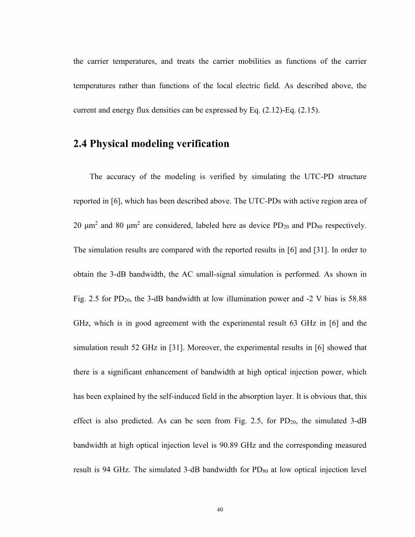
The accuracy of the modeling is verified by simulating the UTC-PD structure
reported in [6], which has been described above. The UTC-PDs with active region area of
20 μm2 and 80 μm2 are considered, labeled here as device PD20 and PD80 respectively.
The simulation results are compared with the reported results in [6] and [31]. In order to
obtain the 3-dB bandwidth, the AC small-signal simulation is performed. As shown in
Fig. 2.5 for PD20, the 3-dB bandwidth at low illumination power and -2 V bias is 58.88
GHz, which is in good agreement with the experimental result 63 GHz in [6] and the
simulation result 52 GHz in [31]. Moreover, the experimental results in [6] showed that
there is a significant enhancement of bandwidth at high optical injection power, which
has been explained by the self-induced field in the absorption layer. It is obvious that, this
effect is also predicted. As can be seen from Fig. 2.5, for PD20, the simulated 3-dB
bandwidth at high optical injection level is 90.89 GHz and the corresponding measured
result is 94 GHz. The simulated 3-dB bandwidth for PD80 at low optical injection level
41
and -2 V bias is 46.25 GHz, which is also comparable with the simulation result 42 GHz
reported in [31]. It can be seen that there is a good agreement between all these
simulation results and the reported results. And the physical modeling successfully
predicted that the bandwidth varies with the change in the device active area, as well as
the change in optical injection level. Consequently, the physics-based simulation is
reliable. In chapter 3 and chapter 4, we will focus on the study of PD80. Additionally, in
all the simulations, the device is biased at -2 V .
0 10 20 30 40 50 60 70 80 90 100
-6
-5
-4
-3
-2
-1
0
Re
lative
RF
re
sp
onse
(d
B)
Frequency (GHz)
Measured in [6]
Simulated in [31]
20 m2, low light intensity
20 m2, high light intensity
80 m2, low light intensity
Figure 2.5 Simulated modulation response of device with active area of 20 and 80 µm2 at -2 V
bias voltage and the reported bandwidth in [6] and [31].
42
2.5 Summary
In this chapter, the physics-based modeling of UTC-PD is described in detail. The
primary properties of InGaAs, InGaAsP and InP, which are the key materials employed
in the studied UTC-PD, are presented. We also introduced the mathematical models
which are implemented in the simulator ATLAS and are used for modeling UTC-PDs in
this work. Furthermore, the accuracy of the modeling is verified by comparing the
simulation results with experimental results. It is demonstrated that the performance of
UTC-PDs can be successfully predicted by using the physics-based modeling method.
43
Chapter 3 Graded Absorption Layer Design
The 3-dB bandwidth of UTC-PD is mainly limited by the carrier transit time τtr and
RC-time constant τRC. If the device performance is not RC-limited, the 3-dB bandwidth
can be improved by decreasing the carrier transit time τtr. For a typical UTC-PD with
uniformly doped absorption layer, the electric field in heavily doped absorption layer is
nearly zero. The minority electrons can only diffuse from absorption layer to the
collection layer. For the UTC-PD with similar absorption layer and collection layer
thickness, the carrier transit time τtr is dominated by the electron transport time τA in the
absorption layer. This is due to the fact that the electron diffusion velocity in the
absorption layer is much smaller than the electron drift velocity in the high electric field
collection layer, and thus the electron drift time in the collection layer is negligible.
Therefore, in order to decrease the carrier transit time, we need to accelerate the minority
electrons in the absorption layer. One approach is to introduce an appropriate built-in
electric field in the absorption layer. Then the electron transport velocity in the absorption
layer can be enhanced effectively. The built-in electric field can be introduced by using
the graded absorption layer structure. This includes two aspects, graded doping structure
and graded bandgap structure. In the following, they will be considered respectively.
44
3.1 Investigation of graded doping effects in absorption layer
The graded doping method is widely used in absorption layer. It can introduce a
built-in electric field to accelerate the minority electrons, and thus reduce the carrier
transit time. For example, the UTC-PD reported by Z. Li et al. [16], a step doping profile
is adopted in the absorption layer. Similarly, a large slope of linearly graded doping
profile is used in the absorption layer of the UTC-PD reported by J.-W. Shi et al., which
can construct a built-in electric field from 2.1 kV/cm to 84 kV/cm [28].
For the studied UTC-PD, PD80, the absorption layer is uniformly doped to 1x10¹⁸
cm-3. In order to investigate the effect of the graded doping method, a linearly graded
doping profile, which replaces the original uniform doping profile in [6], is employed in
the absorption layer. We assume that the doping concentration in the absorption layer
changes linearly from 1.75x1018 cm-3 to 2.5x1017 cm-3, corresponding to the blocking
layer side and the space layer side respectively. It is noted that the average doping
concentration of linear doping is equal to the uniform doping concentration, which is
1.0x1018 cm-3 in the original absorption layer [6]. As shown in Fig. 3.1 and Fig. 3.2, the
effects of the graded doping method can be observed from the electric field distribution in
the 0.22-µm-thickness absorption layer (from 0.07 to 0.29 µm) and the modulation

45
response. The simulation results of the device with linearly doped absorption layer are
compared with the results of the original device, which employs an uniformly doped
absorption layer [6].
0.07 0.11 0.15 0.19 0.23 0.270
2
4
6
8
10
12
Ele
ctr
ic f
ield
(kV
/cm
)
Depth (m)
Uniformly doped absorption layer
Linearly doped absorption layer
Figure 3.1 Distribution of electric field in the absorption layer of PD80 with uniformly and
linearly doped absorption layer.
46
0 10 20 30 40 50 60 70 80 90
-6
-5
-4
-3
-2
-1
0
Rela
tive R
F r
esponse (
dB
)
Frequency (GHz)
Uniformly doped absorption layer
Linearly doped absorption layer
Figure 3.2 Simulated modulation response for PD80 with uniformly and linearly doped
absorption layer.
As can be seen from Fig. 3.1, by using the linearly graded doping profile, the
built-in electric field, which is introduced in the absorption layer, is greater than ~1
kV/cm. This built-in electric field can help the minority electrons move faster, and thus
reduce the electrons transport time in the absorption layer. Therefore, the 3-dB bandwidth
can be enhanced effectively. As plotted in Fig. 3.2 for PD80, the 3-dB bandwidth is
increased from 46.25 GHz to 55.25 GHz, an improvement of 19.5%.
3.2 Design of graded bandgap absorption layer structure
In this study, we propose a new method to construct a built-in electric field in the
absorption layer and to further improve the bandwidth performance. That is, we employ a
47
graded bandgap structure in the absorption layer. The introduced potential gradient can
accelerate the minority electrons in the absorption layer to transport from the diffusion
barrier side to the collection layer side. For the InP and InGaAs material system,
In1-xGaxAsyP1-y or In1-x-yAlxGayAs with lattice matched to InP can provide a range of
bandgaps, which can be used to construct a continuous compositionally-graded bandgap
structure [45]. In this study, the graded bandgap absorption layer is designed by using
In1-xGaxAsyP1-y.
The design of the In1-xGaxAsyP1-y graded bandgap absorption layer is required to
satisfy two conditions. Firstly, we need to ensure that the In1-xGaxAsyP1-y is lattice
matched to InP. Thus, the composition fractions x and y should satisfy the relation given
by Eq. (2.2). Secondly, since we assume the UTC-PD is operated at an optical
wavelength of 1.5 µm, namely the photon energy of the light is 0.82 eV, the energy gap
of the graded absorption region should be no more than 0.82 eV to excite an electron
from the valence band to the conduction band. Thereby, the energy bandgap of
In1-xGaxAsyP1-y should satisfy the following relation, eV82.0)PAsGaIn( y1yxx1 gE . As
mentioned above, the energy bandgap of In1-xGaxAsyP1-y, which is lattice matched to InP,
is given by Eq. (2.1).
48
In order to satisfy the above two conditions, the range of the composition fraction x
is found to be from 0.38 to 0.47. Correspondingly, the range of y is from 0.82 to 1. Thus,
the maximum potential gradient in the absorption region can be formed by adopting
linear compositionally-graded from In0.62Ga0.38As0.82P0.18 to In0.53Ga0.47As.
Accordingly, for PD80, the corresponding graded bandgap absorption layer is
constructed by replacing the original In0.53Ga0.47As absorption layer [6] with a linear
compositionally-graded In0.62Ga0.38As0.82P0.18→In0.53Ga0.47As absorption layer. We
assume that the depth d (in µm) is the distance from a specified point in absorption layer
to the surface of the p-contact layer. Then for PD80, the relation between the composition
fraction x and d can be expressed as 29.0,07.0,351.0409.0 ddx µm. The
corresponding composition fraction y can be calculated according to Eq. (2.2). To
investigate the effect of the graded bandgap absorption structure, we simulated the energy
band diagram and the electric field distribution in the absorption layer. Moreover, the
modulation response is also performed. As illustrated in the following, the simulation
results of the device which employs a graded bandgap absorption layer structure are
compared with the corresponding results of the original device, for which the bandgap of
the InGaAs absorption layer is non-graded [6].
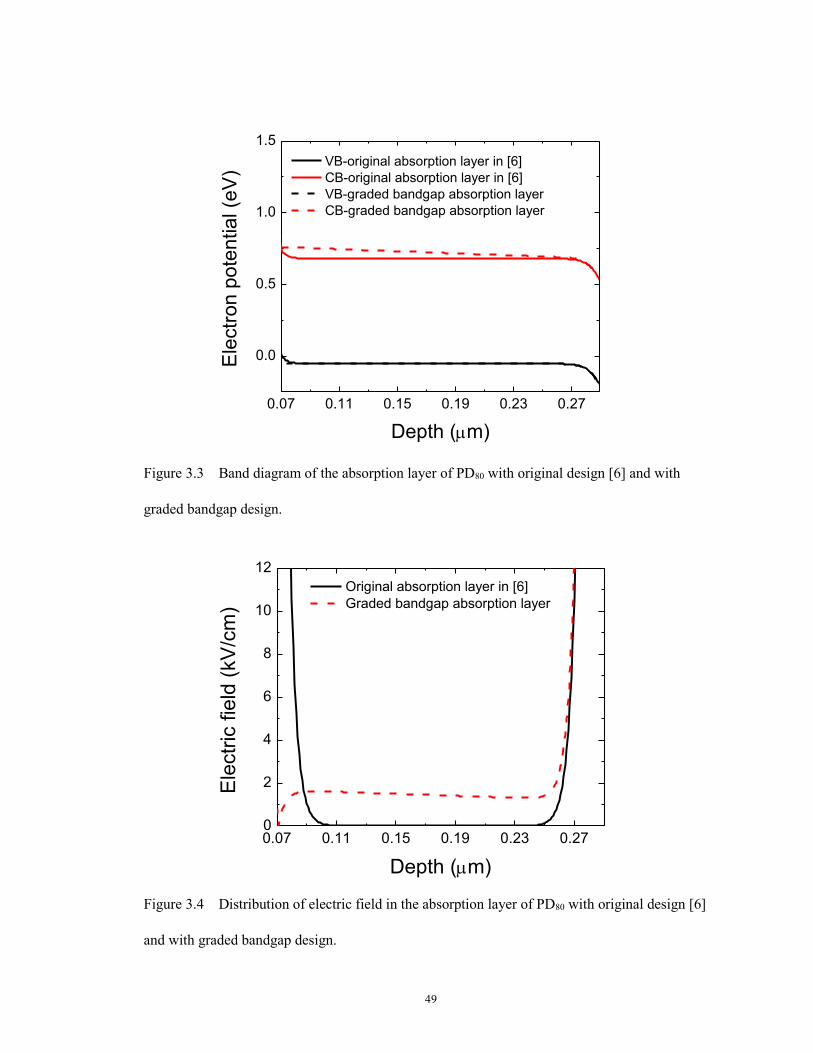
49
0.07 0.11 0.15 0.19 0.23 0.27
0.0
0.5
1.0
1.5
Ele
ctr
on p
ote
ntial (e
V)
Depth (m)
VB-original absorption layer in [6]
CB-original absorption layer in [6]
VB-graded bandgap absorption layer
CB-graded bandgap absorption layer
Figure 3.3 Band diagram of the absorption layer of PD80 with original design [6] and with
graded bandgap design.
0.07 0.11 0.15 0.19 0.23 0.270
2
4
6
8
10
12
Ele
ctr
ic fie
ld (
kV
/cm
)
Depth (m)
Original absorption layer in [6]
Graded bandgap absorption layer
Figure 3.4 Distribution of electric field in the absorption layer of PD80 with original design [6]
and with graded bandgap design.
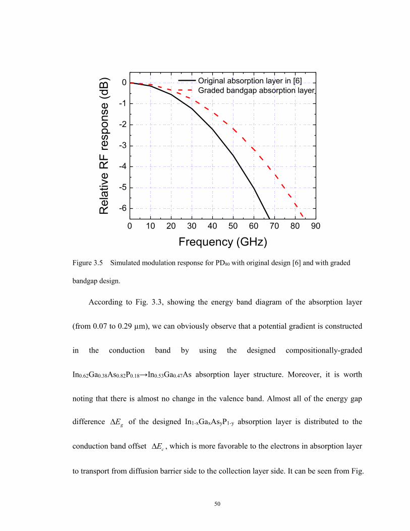
50
0 10 20 30 40 50 60 70 80 90
-6
-5
-4
-3
-2
-1
0
Rela
tive R
F r
esponse (
dB
)
Frequency (GHz)
Original absorption layer in [6]
Graded bandgap absorption layer
Figure 3.5 Simulated modulation response for PD80 with original design [6] and with graded
bandgap design.
According to Fig. 3.3, showing the energy band diagram of the absorption layer
(from 0.07 to 0.29 µm), we can obviously observe that a potential gradient is constructed
in the conduction band by using the designed compositionally-graded
In0.62Ga0.38As0.82P0.18→In0.53Ga0.47As absorption layer structure. Moreover, it is worth
noting that there is almost no change in the valence band. Almost all of the energy gap
difference gE of the designed In1-xGaxAsyP1-y absorption layer is distributed to the
conduction band offset cE , which is more favorable to the electrons in absorption layer
to transport from diffusion barrier side to the collection layer side. It can be seen from Fig.
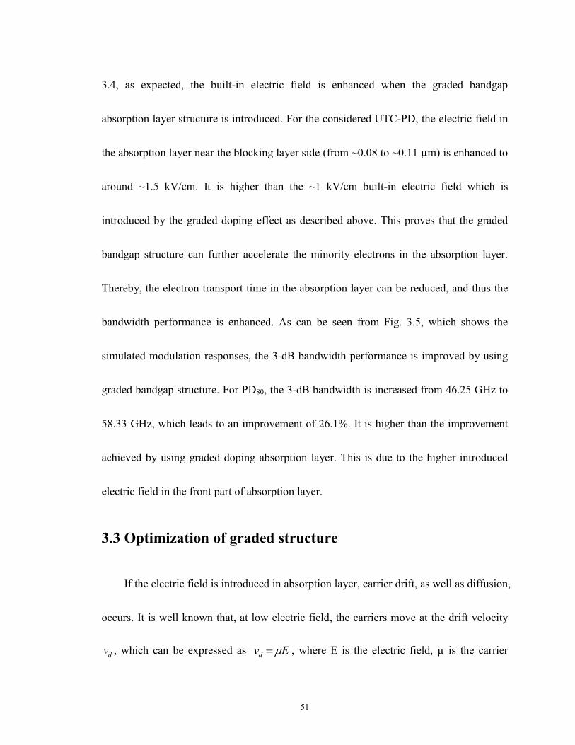
51
3.4, as expected, the built-in electric field is enhanced when the graded bandgap
absorption layer structure is introduced. For the considered UTC-PD, the electric field in
the absorption layer near the blocking layer side (from ~0.08 to ~0.11 µm) is enhanced to
around ~1.5 kV/cm. It is higher than the ~1 kV/cm built-in electric field which is
introduced by the graded doping effect as described above. This proves that the graded
bandgap structure can further accelerate the minority electrons in the absorption layer.
Thereby, the electron transport time in the absorption layer can be reduced, and thus the
bandwidth performance is enhanced. As can be seen from Fig. 3.5, which shows the
simulated modulation responses, the 3-dB bandwidth performance is improved by using
graded bandgap structure. For PD80, the 3-dB bandwidth is increased from 46.25 GHz to
58.33 GHz, which leads to an improvement of 26.1%. It is higher than the improvement
achieved by using graded doping absorption layer. This is due to the higher introduced
electric field in the front part of absorption layer.
3.3 Optimization of graded structure
If the electric field is introduced in absorption layer, carrier drift, as well as diffusion,
occurs. It is well known that, at low electric field, the carriers move at the drift velocity
dv , which can be expressed as Evd , where E is the electric field, µ is the carrier

52
mobility. While, at higher electric field, the carrier energy obtained from electric field is
transferred to lattice rather than increasing the velocity. As can been seen from Fig. 2.3
[40], for InGaAs and InP, the electron velocity no longer increases proportionally with
increasing electric field. And after a peak value, drift velocity decreases as the electric
field goes higher. Finally, drift velocity tends to saturation. On the other hand, for carrier
diffusion, the diffusion coefficient D indicates how well the carrier moves due to the
density gradient. The relation between diffusion coefficient and carrier mobility is given
by q
kTD . Consequently, the optimum performance can be obtained if appropriate
electric field E and carrier mobility µ are found.
As discussed in the previous section, the graded structure, including graded doping
and graded bandgap structure, mainly contributes to increase the built-in electric field E
in the absorption layer. In addition, the graded structure also has impacts on carrier
mobility µ. This can be explained as follows. For the graded doping method, the doping
concentration will be affected, and the carrier mobility is the function of the doping
concentration. As the doping concentration increases, the ionized impurity scattering
mechanism will lead to the carrier mobility µ decrease. On the other hand, the carrier
mobility can be expressed as
m
qτμ , where q is the elementary charge, τ is the mean
time between collisions and m* is the carrier effective mass. In the In1-xGaxAsyP1-y

53
system, the effective mass of carrier depends on the composition fractions x and y.
Thereby, for the graded bandgap method, the variation of the composition fractions has
influence on the effective mass m*, and thus the carrier mobility is affected. As the
composition fraction y increases, both the hole and electron effective masses decrease
[33][46], which implies that the carrier mobility will increase. According to the above
analysis, we can optimize the graded structure to find the optimal electric field E and
carrier mobility µ to enhance the carrier transport velocity.
It is found that, as the doping concentration gradient or energy bandgap gradient
becomes larger, the introduced built-in electric field increases. Thus, in order to create
higher built-in electric field which leads to higher drift velocity, we need to construct
larger slope of the gradient. The slope can be increased if we shorten the absorption layer
or construct larger potential and doping difference. However, shortening the absorption
layer leads to lower responsivity. This is because, for the studied UTC-PD, the absorption
layer thickness is much shorter than the penetration depth [47], and the responsivity
scales down with reduced absorption thickness. On the other hand, the potential
difference can not be improved due to the limitation of the second condition as mentioned
above. The doping difference can be enhanced by increasing the doping concentration
near the diffusion barrier side or decreasing the doping concentration near collector side.
54
While, higher doping concentration results in lower carrier mobility and lower carrier
lifetime, which lead to the responsivity and bandwidth drop. Reducing the doping
concentration near the collector side does not have much impact on the slope, due to its
small order of magnitude. Therefore, these methods are inappropriate. As can be seen
from Fig. 3.1 and Fig. 3.4, the improvement of the built-in electric field in the absorption
layer near the space layer side (from 0.26 to 0.29 µm) is not significant by using the
graded structure. Moreover, according to the comparison between Fig. 3.1 and Fig. 3.4,
as well as the corresponding 3-dB bandwidth, it is found that higher electric field in the
front part of absorption layer leads to better 3-dB bandwidth performance. Thus, as
indicated in Fig. 3.6, a feasible way to enhance the built-in electric field is to use a
partially graded structure. The absorption layer thickness WA is maintained unchanged,
and only the graded structure thickness WG is shortened (In the following sections, WGD
is the thickness of graded doping region, WGB is the thickness of graded bandgap region).
Thereby, the slope of the gradient can be enlarged to create a high electric field in the
front part of absorption layer. Meanwhile, the required conditions, for the design of
energy band, can be satisfied. In the following, we will investigate the modified graded
doping and graded bandgap structure respectively. For PD80, the absorption layer
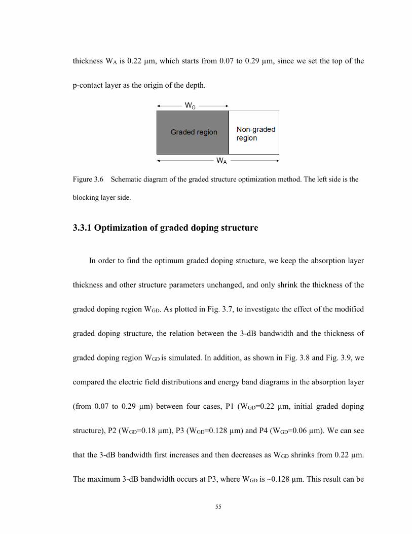
55
thickness WA is 0.22 µm, which starts from 0.07 to 0.29 µm, since we set the top of the
p-contact layer as the origin of the depth.
Figure 3.6 Schematic diagram of the graded structure optimization method. The left side is the
blocking layer side.
3.3.1 Optimization of graded doping structure
In order to find the optimum graded doping structure, we keep the absorption layer
thickness and other structure parameters unchanged, and only shrink the thickness of the
graded doping region WGD. As plotted in Fig. 3.7, to investigate the effect of the modified
graded doping structure, the relation between the 3-dB bandwidth and the thickness of
graded doping region WGD is simulated. In addition, as shown in Fig. 3.8 and Fig. 3.9, we
compared the electric field distributions and energy band diagrams in the absorption layer
(from 0.07 to 0.29 µm) between four cases, P1 (WGD=0.22 µm, initial graded doping
structure), P2 (WGD=0.18 µm), P3 (WGD=0.128 µm) and P4 (WGD=0.06 µm). We can see
that the 3-dB bandwidth first increases and then decreases as WGD shrinks from 0.22 µm.
The maximum 3-dB bandwidth occurs at P3, where WGD is ~0.128 µm. This result can be
56
explained as follows. The slope of the doping concentration gradient increases as WGD
shrinks from 0.22 µm. At first, as can be seen from Fig. 3.8, the built-in electric field in
the graded doping region is enhanced, such as case P2. At the same time, the average
doping concentration in the absorption layer decreases as WGD shrinks. It implies that the
carrier mobility is improved. Thereby, the carrier drift velocity increases. Additionally, as
shown in Fig. 3.9, the depletion region in the absorption layer becomes wider since the
doping concentration drops. In this depletion region, the carriers drift rather than
diffusion. Besides, the junction capacitor is reduced as a result of the wider depletion
region. Because of all these reasons, the carrier transit time and RC-time constant will be
reduced. Therefore, the 3-dB bandwidth performance is improved. However, as the
graded doping region further shrinks, the interface between the graded and non-graded
region will be gradually away from the high electric field region near the space layer side,
which in fact is the depletion region in the absorption layer. When this interface is out of
the depletion region, the electric field in the non-graded doping region near this interface
likely to be low, since the built-in electric field enhancement only occurs in the graded
doping region. Thus, as can be observed in Fig. 3.8, due to the trade-off between the
increased carrier mobility and the decreased electric field, the 3-dB bandwidth first
increases to the maximum case P3, in which the built-in electric field in the non-graded
57
region near the interface (from ~0.198 to ~0.24 µm) is lower than that in case P2. Then,
the bandwidth starts to drop. On the other hand, as illustrated in Fig. 2.3 [40], when the
built-in electric field in the graded doping region becomes further higher, the carrier drift
velocity in this region may decrease from the peak value to saturation, due to the
reduction of carrier mobility. Consequently, the 3-dB bandwidth performance becomes
worse. For example, case P4, although the built-in electric field near the blocking layer
side (from 0.07 to ~0.135 µm), which is generated by large doping gradient, is the highest,
the bandwidth performance is limited by the low electric field in the non-graded doping
region. For PD80, as can be seen from Fig. 3.7, the optimal thickness of graded doping
region is found to be ~0.128 µm. The 3-dB bandwidth improvement, from P1 55.25 GHz
to P3 60.67 GHz, is 9.8%.
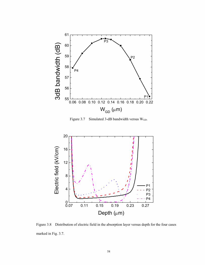
58
0.06 0.08 0.10 0.12 0.14 0.16 0.18 0.20 0.2255
56
57
58
59
60
61
P3
P4
P2
3d
B b
an
dw
idth
(d
B)
WGD
(m)
P1
Figure 3.7 Simulated 3-dB bandwidth versus WGD.
0.07 0.11 0.15 0.19 0.23 0.270
4
8
12
16
20
Ele
ctr
ic f
ield
(kV
/cm
)
Depth (m)
P1
P2
P3
P4
Figure 3.8 Distribution of electric field in the absorption layer versus depth for the four cases
marked in Fig. 3.7.
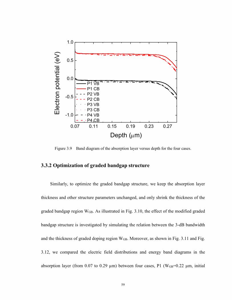
59
0.07 0.11 0.15 0.19 0.23 0.27
-1.0
-0.5
0.0
0.5
1.0
Ele
ctr
on
po
ten
tia
l (e
V)
Depth (m)
P1 VB
P1 CB
P2 VB
P2 CB
P3 VB
P3 CB
P4 VB
P4 CB
Figure 3.9 Band diagram of the absorption layer versus depth for the four cases.
3.3.2 Optimization of graded bandgap structure
Similarly, to optimize the graded bandgap structure, we keep the absorption layer
thickness and other structure parameters unchanged, and only shrink the thickness of the
graded bandgap region WGB. As illustrated in Fig. 3.10, the effect of the modified graded
bandgap structure is investigated by simulating the relation between the 3-dB bandwidth
and the thickness of graded doping region WGB. Moreover, as shown in Fig. 3.11 and Fig.
3.12, we compared the electric field distributions and energy band diagrams in the
absorption layer (from 0.07 to 0.29 µm) between four cases, P1 (WGB=0.22 µm, initial
60
graded bandgap structure), P2 (WGB=0.20 µm), P3 (WGB=0.18 µm) and P4 (WGB=0.14
µm). According to Fig. 3.10, as expected, the 3-dB bandwidth first increases and then
decreases as WGB shrinks from 0.22 µm. The maximum 3-dB bandwidth occurs at P3,
where WGB is ~0.18 µm. This result can be understood as follows. As the graded bandgap
region shrinks from 0.22 µm, the slope of the potential gradient in conduction band
increases, which can be seen from Fig. 3.12. Correspondingly, such as the case P2 plotted
in Fig. 3.11, the built-in electric field in the graded bandgap region is enhanced. On the
other hand, the average composition fraction y of the In1-xGaxAsyP1-y system in
absorption layer becomes larger as WGB shrinks. Thus, both the effective masses of hole
and electron decrease [33], which implies that the carrier mobility is improved, since the
carrier mobility is inversely proportional to the carrier effective mass. Thereby, the
carrier drift velocity increases, which leads to less carrier transit time. Consequently, the
3-dB bandwidth is enhanced. However, as the built-in electric field becomes further
higher, the carrier drift velocity may decrease from the peak value, and the carrier
mobility starts to drop. In addition, as the graded bandgap region shrinks, similar to the
case of graded doping, the interface between the graded and non-graded region will be
gradually away from the high electric field depletion region in the absorption layer near
space layer side. Because the built-in electric field can be only constructed in the graded
61
bandgap region, when the interface is out of the depletion region, the electric field in the
non-graded bandgap region near this interface drops significantly. Such as case P4,
although the built-in electric field near the blocking layer side (from 0.07 to ~0.20 µm),
which is created by the large bandgap gradient, is the highest, the carrier cannot be
accelerated effectively due to the low electric field (from ~0.21 to ~0.25 µm) in the
non-graded bandgap region. Therefore, the performance of 3-dB bandwidth declines. It is
noted that, as can be seen from Fig. 3.11, although the maximum improvement of 3-dB
bandwidth occurs at P3, its built-in electric field in the non-graded region near the
interface (from 0.24 to 0.26 µm) is lower than that in case P2. This is due to the trade-off
between the increased carrier mobility and the decreased electric field. For PD80, as
shown in Fig. 3.10, the optimal thickness of graded bandgap region is ~0.18 µm. The
3-dB bandwidth is improved from P1 58.33 GHz to P3 59.07 GHz, an improvement of
1.3%, which is not as significant as the improvement of optimized graded doping
structure. This is because the optimized graded doping structure leads to a wider
depletion region in the absorption layer.
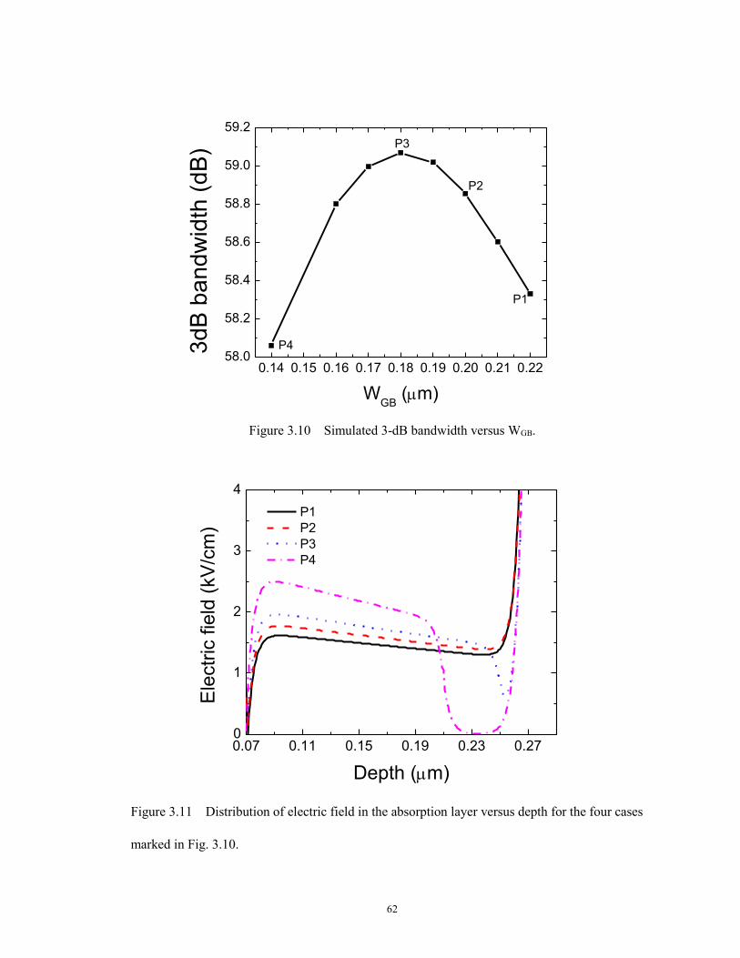
62
0.14 0.15 0.16 0.17 0.18 0.19 0.20 0.21 0.2258.0
58.2
58.4
58.6
58.8
59.0
59.2
P1
P2
P3
3d
B b
an
dw
idth
(d
B)
WGB
(m)
P4
Figure 3.10 Simulated 3-dB bandwidth versus WGB.
0.07 0.11 0.15 0.19 0.23 0.270
1
2
3
4
Ele
ctr
ic fie
ld (
kV
/cm
)
Depth (m)
P1
P2
P3
P4
Figure 3.11 Distribution of electric field in the absorption layer versus depth for the four cases
marked in Fig. 3.10.
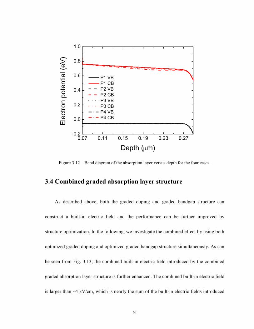
63
0.07 0.11 0.15 0.19 0.23 0.27-0.2
0.0
0.2
0.4
0.6
0.8
1.0
Ele
ctr
on
po
ten
tia
l (e
V)
Depth (m)
P1 VB
P1 CB
P2 VB
P2 CB
P3 VB
P3 CB
P4 VB
P4 CB
Figure 3.12 Band diagram of the absorption layer versus depth for the four cases.
3.4 Combined graded absorption layer structure
As described above, both the graded doping and graded bandgap structure can
construct a built-in electric field and the performance can be further improved by
structure optimization. In the following, we investigate the combined effect by using both
optimized graded doping and optimized graded bandgap structure simultaneously. As can
be seen from Fig. 3.13, the combined built-in electric field introduced by the combined
graded absorption layer structure is further enhanced. The combined built-in electric field
is larger than ~4 kV/cm, which is nearly the sum of the built-in electric fields introduced
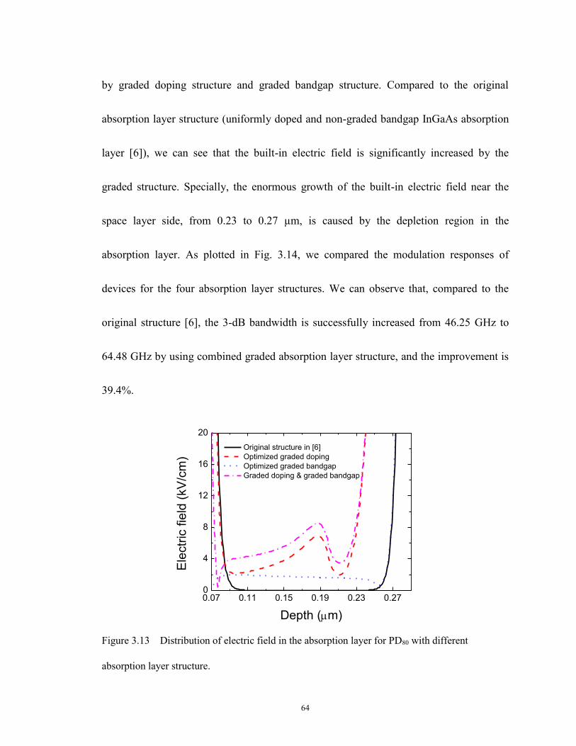
64
by graded doping structure and graded bandgap structure. Compared to the original
absorption layer structure (uniformly doped and non-graded bandgap InGaAs absorption
layer [6]), we can see that the built-in electric field is significantly increased by the
graded structure. Specially, the enormous growth of the built-in electric field near the
space layer side, from 0.23 to 0.27 µm, is caused by the depletion region in the
absorption layer. As plotted in Fig. 3.14, we compared the modulation responses of
devices for the four absorption layer structures. We can observe that, compared to the
original structure [6], the 3-dB bandwidth is successfully increased from 46.25 GHz to
64.48 GHz by using combined graded absorption layer structure, and the improvement is
39.4%.
0.07 0.11 0.15 0.19 0.23 0.270
4
8
12
16
20
Ele
ctr
ic fie
ld (
kV
/cm
)
Depth (m)
Original structure in [6]
Optimized graded doping
Optimized graded bandgap
Graded doping & graded bandgap
Figure 3.13 Distribution of electric field in the absorption layer for PD80 with different
absorption layer structure.
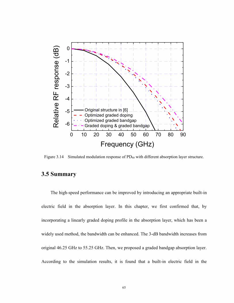
65
0 10 20 30 40 50 60 70 80 90
-6
-5
-4
-3
-2
-1
0
Rela
tive R
F r
esponse (
dB
)
Frequency (GHz)
Original structure in [6]
Optimized graded doping
Optimized graded bandgap
Graded doping & graded bandgap
Figure 3.14 Simulated modulation response of PD80 with different absorption layer structure.
3.5 Summary
The high-speed performance can be improved by introducing an appropriate built-in
electric field in the absorption layer. In this chapter, we first confirmed that, by
incorporating a linearly graded doping profile in the absorption layer, which has been a
widely used method, the bandwidth can be enhanced. The 3-dB bandwidth increases from
original 46.25 GHz to 55.25 GHz. Then, we proposed a graded bandgap absorption layer.
According to the simulation results, it is found that a built-in electric field in the
66
absorption layer can be constructed by applying the graded bandgap structure. This
method leads to a 3-dB bandwidth of 58.33 GHz. The better performance is caused by the
higher introduced built-in electric field in the front part of absorption layer. Furthermore,
by using partially graded absorption layer structure, these two methods are optimized
respectively. By the optimization of graded doping structure, the 3-dB bandwidth raised
to 60.67 GHz. On the other hand, the bandwidth performance of the optimum graded
bandgap structure is 59.07 GHz. Since the optimized graded doping structure leads to a
wider depletion region in the absorption layer, the bandwidth performance improvement
is greater. Finally, the bandwidth performance of the UTC-PD with combined graded
absorption layer structure is investigated. A 3-dB bandwidth of 64.48 GHz is predicted,
the improvement is 39.4%. And it is found that, the combined introduced built-in electric
field is nearly the sum of the built-in electric fields created by graded doping structure
and graded bandgap structure.
67
Chapter 4 Investigation and Design of Collection
Layer Doping Profile
It is well known that the space-charge effect is the primary mechanism which causes
saturation at high current level in photodiodes [48]. At high optical injection level, the
electric field in the depletion region will redistribute due to the space-charge effect,
which may result in reduced electron velocity and degradation of the bandwidth and
output power. It has been suggested that the space-charge suppression of the electric field
could be compensated by a fixed distribution of background dopants [49]. Thus, the
doping concentration in the depleted InP collection layer is very important, since it is
directly relevant to the saturation performance. By appropriately doping the depletion
region, the electric field distribution can be adjusted. Thereby, the space-charge effect
can be reduced, and the saturation performance can be improved effectively. In addition,
there is another advantage by using the technique of charge compensation. Unlike the
method, which relieves the space-charge effect by increasing the bias voltage, charge
compensation method will not lead to thermal effect. In the following, the space-charge
effect in the collector and the technique of charge compensation with various doping
levels are first investigated by analyzing the energy band profile and the distribution of
68
the electric field. According to the analysis, we proposed a new collection layer design
based on linear doping profile. Furthermore, it is found that the saturation performance
can be further improved by using Gaussian doping profile in the collection layer.
4.1 Space-charge effect in UTC-PDs
In order to analyze the space-charge effect, we investigated electron concentration
profiles, the distributions of electric field in the collection layer, and also the energy band
structures at different optical injection levels. As shown in Fig. 4.1, at high light intensity,
the distribution of electron concentration in the absorption layer (from 0.07 to 0.29 µm) is
different from the cases of low optical injection levels. There is a significant difference in
the electron concentration profile when the light intensity is higher than 2x10⁶ W/cm2.
The electron concentration near the absorption layer and space layer interface (from
~0.25 to 0.29 µm) is higher than that near the blocking layer and absorption layer
interface (from 0.07 to ~0.11 µm). This implies that, as the optical power goes higher, the
electron starts to accumulate near the absorption layer and space layer interface. Then, as
the light intensity further increases, more electrons will be accumulated in the absorption
layer due to the fact that the electron cannot effectively transport from the absorption
layer to the collection layer. This can be seen from the case in Fig. 4.1, in which the light
69
intensity is 2.25x10⁶ W/cm2. The accumulation of electrons in the absorption layer
greatly increases the carrier recombination probability, which leads to the responsivity
reduction. Moreover, the higher concentration of electrons in the absorption layer near
the space layer end hinders the diffusion of electrons from the absorption layer to the
collection layer to some extent and shows a tendency toward saturation. In addition, the
accumulated electrons will introduce an electric field which is reverse to the applied
electric field. This will cause adverse effect on the internal electric field. It can be seen
from the distribution of electric field in Fig. 4.2, as the optical power raises, the electric
field drops in the space layer (from 0.30 to 0.32 µm), cliff layer (from 0.32 to 0.327 µm),
and also the input end of collection layer (from 0.327 to ~0.437 µm). On the other hand,
it is illustrated in Fig. 4.3, as the light intensity increases, the excess carrier bends the
energy bands. The energy bands in the collection layer near the absorption end (from
0.327 to ~0.437 µm) become flatter and those near the subcollection end (from ~0.437 to
0.59 µm) become steeper. This indicates the corresponding changes of the electric field in
the collection layer (from 0.327 to 0.59 µm). As shown in Fig. 4.2, when the optical
injection level increases, the electric field near the absorption end (from 0.327 to ~0.437
µm) is reduced and it increases near the subcollection end (from ~0.437 to 0.59 µm).
These simulation results are in agreement with the report of T. Ishibashi et al. [6]. If the
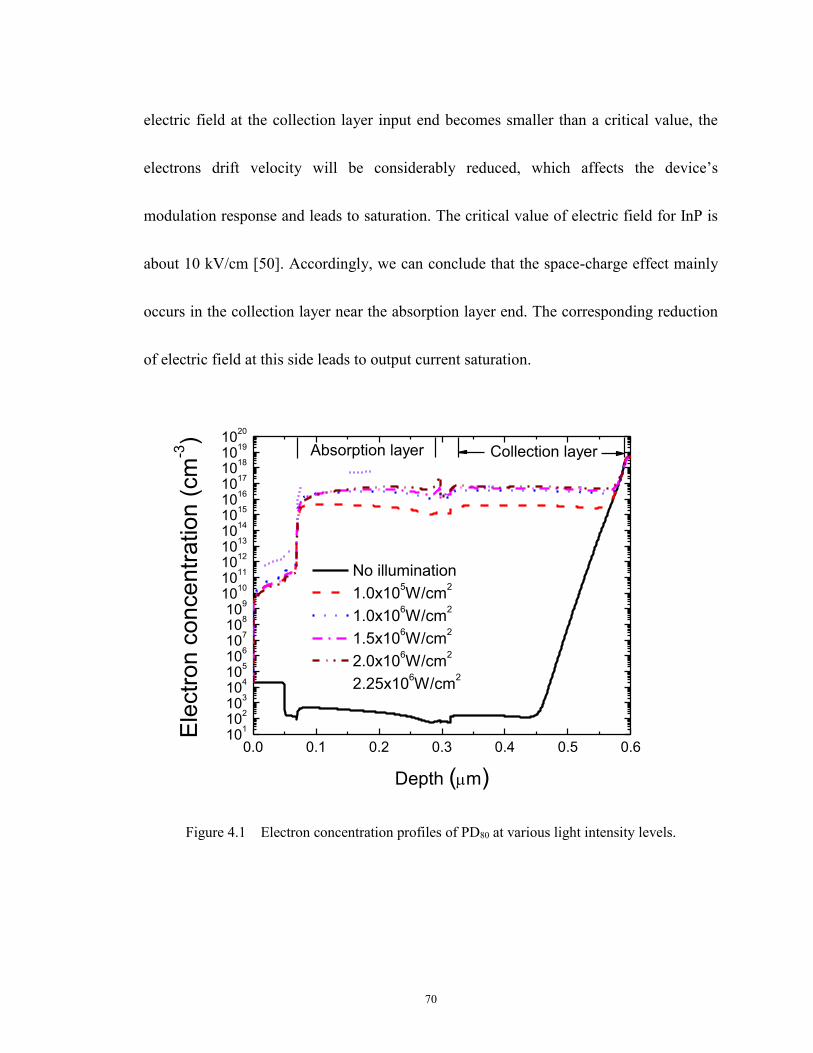
70
electric field at the collection layer input end becomes smaller than a critical value, the
electrons drift velocity will be considerably reduced, which affects the device’s
modulation response and leads to saturation. The critical value of electric field for InP is
about 10 kV/cm [50]. Accordingly, we can conclude that the space-charge effect mainly
occurs in the collection layer near the absorption layer end. The corresponding reduction
of electric field at this side leads to output current saturation.
0.0 0.1 0.2 0.3 0.4 0.5 0.610
110
210
310
410
510
610
710
810
910
1010
1110
1210
1310
1410
1510
1610
1710
1810
1910
20
Ele
ctr
on
co
nce
ntr
atio
n (
cm
-3)
Depth (m)
No illumination
1.0x10⁵W/cm
2
1.0x10⁶W/cm
2
1.5x10⁶W/cm
2
2.0x10⁶W/cm
2
2.25x10⁶W/cm
2
Absorption layer Collection layer
Figure 4.1 Electron concentration profiles of PD80 at various light intensity levels.
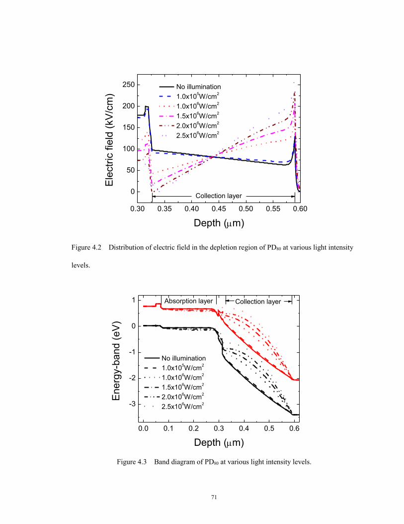
71
0.30 0.35 0.40 0.45 0.50 0.55 0.60
0
50
100
150
200
250
Collection layer
No illumination
1.0x10⁵W/cm
2
1.0x10⁶W/cm
2
1.5x10⁶W/cm
2
2.0x10⁶W/cm
2
2.5x10⁶W/cm
2
Ele
ctr
ic fie
ld (
kV
/cm
)
Depth (m)
Figure 4.2 Distribution of electric field in the depletion region of PD80 at various light intensity
levels.
0.0 0.1 0.2 0.3 0.4 0.5 0.6
-3
-2
-1
0
1
Energ
y-b
and (
eV
)
Depth (m)
No illumination
1.0x10⁵W/cm
2
1.0x10⁶W/cm
2
1.5x10⁶W/cm
2
2.0x10⁶W/cm
2
2.5x10⁶W/cm
2
Absorption layer Collection layer
Figure 4.3 Band diagram of PD80 at various light intensity levels.
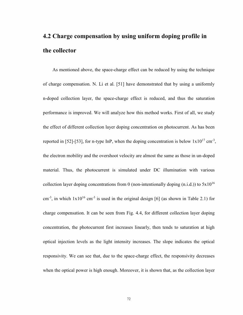
72
4.2 Charge compensation by using uniform doping profile in
the collector
As mentioned above, the space-charge effect can be reduced by using the technique
of charge compensation. N. Li et al. [51] have demonstrated that by using a uniformly
n-doped collection layer, the space-charge effect is reduced, and thus the saturation
performance is improved. We will analyze how this method works. First of all, we study
the effect of different collection layer doping concentration on photocurrent. As has been
reported in [52]-[53], for n-type InP, when the doping concentration is below 1x1017 cm-3,
the electron mobility and the overshoot velocity are almost the same as those in un-doped
material. Thus, the photocurrent is simulated under DC illumination with various
collection layer doping concentrations from 0 (non-intentionally doping (n.i.d.)) to 5x10¹⁶
cm-3, in which 1x1016 cm-3 is used in the original design [6] (as shown in Table 2.1) for
charge compensation. It can be seen from Fig. 4.4, for different collection layer doping
concentration, the photocurrent first increases linearly, then tends to saturation at high
optical injection levels as the light intensity increases. The slope indicates the optical
responsivity. We can see that, due to the space-charge effect, the responsivity decreases
when the optical power is high enough. Moreover, it is shown that, as the collection layer
73
doping concentration goes higher, the DC saturation current increases. This implies that
higher average doping level in the collection layer may lead to better saturation
performance. According to the distribution of electric field in the collection layer (from
0.327 to 0.59 µm) without optical injection and at high optical injection level (the light
intensity is 2x10⁶ W/cm2), which is shown in Fig. 4.5 and Fig. 4.6, we can see that the
saturation current is improved because of the increased electric field in the collection
layer near the absorption layer end (from 0.327 to ~0.437 µm). However, as seen in Fig.
4.7, when the doping concentration is high enough, the energy bands in the collection
layer near the subcollection end (from ~0.52 to 0.59 µm) become flatter. This implies that
the collection layer cannot be completely depleted at normal device operation bias
voltage. As the depletion region shrinks, it cannot extend to the InP subcollection layer,
which leads to higher junction capacitance and series resistance. The electrons in the
collection layer cannot be rapidly swept into the subcollection layer to form the
photocurrent. Therefore, the bandwidth performance degradation occurs at high
collection layer doping concentration. Although we can adopt a higher bias voltage to
fully deplete the collection layer and also reduce the space-charge effect, the heat power
will increase and thus leads to device thermal failure. Consequently, for the considered
UTC-PD, there is a proper uniform doping concentration range to obtain better
74
performance. It is found to be around 2x1016 cm-3 to 3x1016 cm-3. As plotted in Fig. 4.8,
which is obtained from the modulation response, we investigated the variation of 3-dB
bandwidth performance with increasing average photocurrent for different uniform
doping levels. Among them, the uniform doping level of 1x1016 cm-3 is the original
design [6]. We can observe that, for each case, 3-dB bandwidth first increases with the
injection power, then decreases due to output saturation. The self-induced electric field in
the absorption layer has explained the increase of bandwidth [6]. Moreover, it is shown
that, as analyzed above, bandwidth decreases with increasing doping concentration.
While, since the saturation performance is improved by increasing doping concentration,
the degradation of 3-dB bandwidth occurs at higher photocurrent. We found that, for
PD80, the appropriate uniform doping concentration in the collection layer is 2x1016 cm-3.
Comparing this case with the case of 1x1016 cm-3, which is the original design [6], the
saturation current is enhanced and the bandwidth is slightly reduced. In the following
sections, the UTC-PD, in which the collection layer is uniformly doped to 2x1016 cm-3, is
used for comparison.
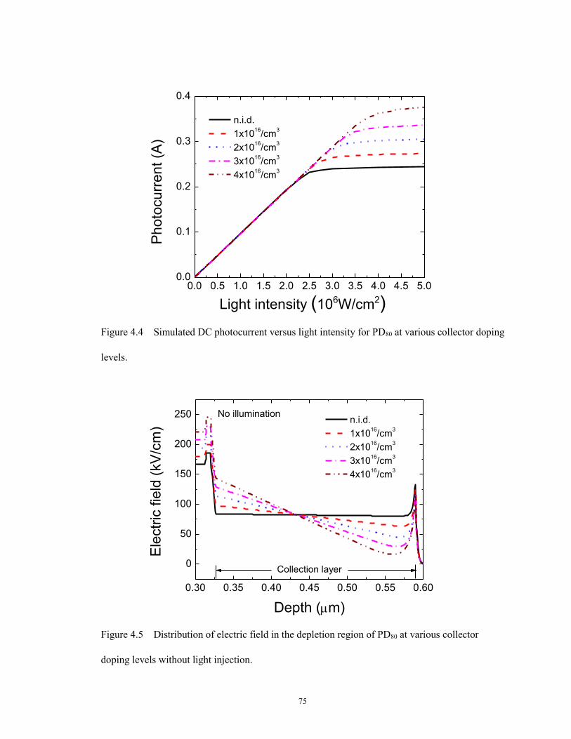
75
0.0 0.5 1.0 1.5 2.0 2.5 3.0 3.5 4.0 4.5 5.00.0
0.1
0.2
0.3
0.4
Ph
oto
cu
rre
nt
(A)
Light intensity (106W/cm2)
n.i.d.
1x10¹⁶
/cm3
2x10¹⁶
/cm3
3x10¹⁶
/cm3
4x10¹⁶
/cm3
Figure 4.4 Simulated DC photocurrent versus light intensity for PD80 at various collector doping
levels.
0.30 0.35 0.40 0.45 0.50 0.55 0.60
0
50
100
150
200
250
Ele
ctr
ic fie
ld (
kV
/cm
)
Depth (m)
n.i.d.
1x10¹⁶
/cm3
2x10¹⁶
/cm3
3x10¹⁶
/cm3
4x10¹⁶
/cm3
No illumination
Collection layer
Figure 4.5 Distribution of electric field in the depletion region of PD80 at various collector
doping levels without light injection.
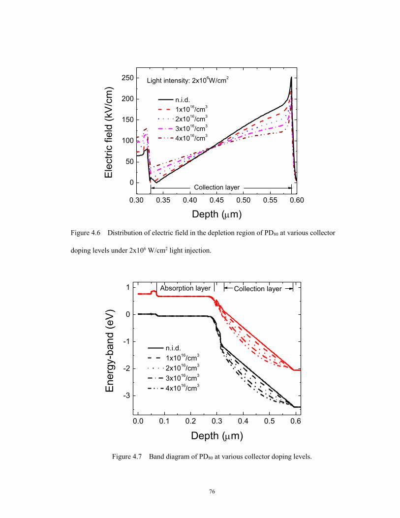
76
0.30 0.35 0.40 0.45 0.50 0.55 0.60
0
50
100
150
200
250
Depth (m)
Ele
ctr
ic f
ield
(kV
/cm
) n.i.d.
1x10¹⁶
/cm3
2x10¹⁶
/cm3
3x10¹⁶
/cm3
4x10¹⁶
/cm3
Light intensity: 2x10⁶W/cm
2
Collection layer
Figure 4.6 Distribution of electric field in the depletion region of PD80 at various collector
doping levels under 2x10⁶ W/cm2 light injection.
0.0 0.1 0.2 0.3 0.4 0.5 0.6
-3
-2
-1
0
1
Energ
y-b
and (
eV
)
Depth (m)
n.i.d.
1x10¹⁶
/cm3
2x10¹⁶
/cm3
3x10¹⁶
/cm3
4x10¹⁶
/cm3
Absorption layer Collection layer
Figure 4.7 Band diagram of PD80 at various collector doping levels.
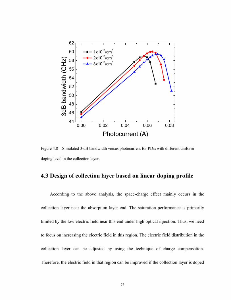
77
0.00 0.02 0.04 0.06 0.0844
46
48
50
52
54
56
58
60
62
3dB
bandw
idth
(G
Hz)
Photocurrent (A)
1x10¹⁶
/cm3
2x10¹⁶
/cm3
3x10¹⁶
/cm3
Figure 4.8 Simulated 3-dB bandwidth versus photocurrent for PD80 with different uniform
doping level in the collection layer.
4.3 Design of collection layer based on linear doping profile
According to the above analysis, the space-charge effect mainly occurs in the
collection layer near the absorption layer end. The saturation performance is primarily
limited by the low electric field near this end under high optical injection. Thus, we need
to focus on increasing the electric field in this region. The electric field distribution in the
collection layer can be adjusted by using the technique of charge compensation.
Therefore, the electric field in that region can be improved if the collection layer is doped
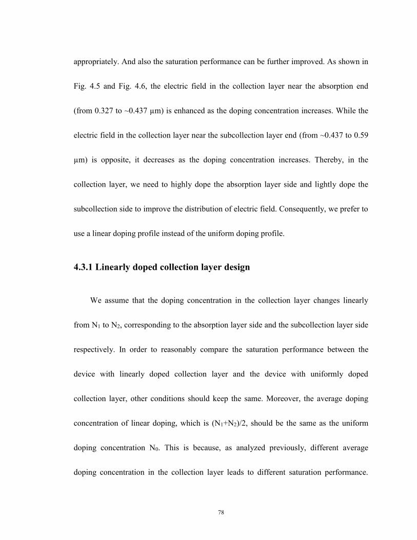
78
appropriately. And also the saturation performance can be further improved. As shown in
Fig. 4.5 and Fig. 4.6, the electric field in the collection layer near the absorption end
(from 0.327 to ~0.437 µm) is enhanced as the doping concentration increases. While the
electric field in the collection layer near the subcollection layer end (from ~0.437 to 0.59
µm) is opposite, it decreases as the doping concentration increases. Thereby, in the
collection layer, we need to highly dope the absorption layer side and lightly dope the
subcollection side to improve the distribution of electric field. Consequently, we prefer to
use a linear doping profile instead of the uniform doping profile.
4.3.1 Linearly doped collection layer design
We assume that the doping concentration in the collection layer changes linearly
from N1 to N2, corresponding to the absorption layer side and the subcollection layer side
respectively. In order to reasonably compare the saturation performance between the
device with linearly doped collection layer and the device with uniformly doped
collection layer, other conditions should keep the same. Moreover, the average doping
concentration of linear doping, which is (N1+N2)/2, should be the same as the uniform
doping concentration N0. This is because, as analyzed previously, different average
doping concentration in the collection layer leads to different saturation performance.
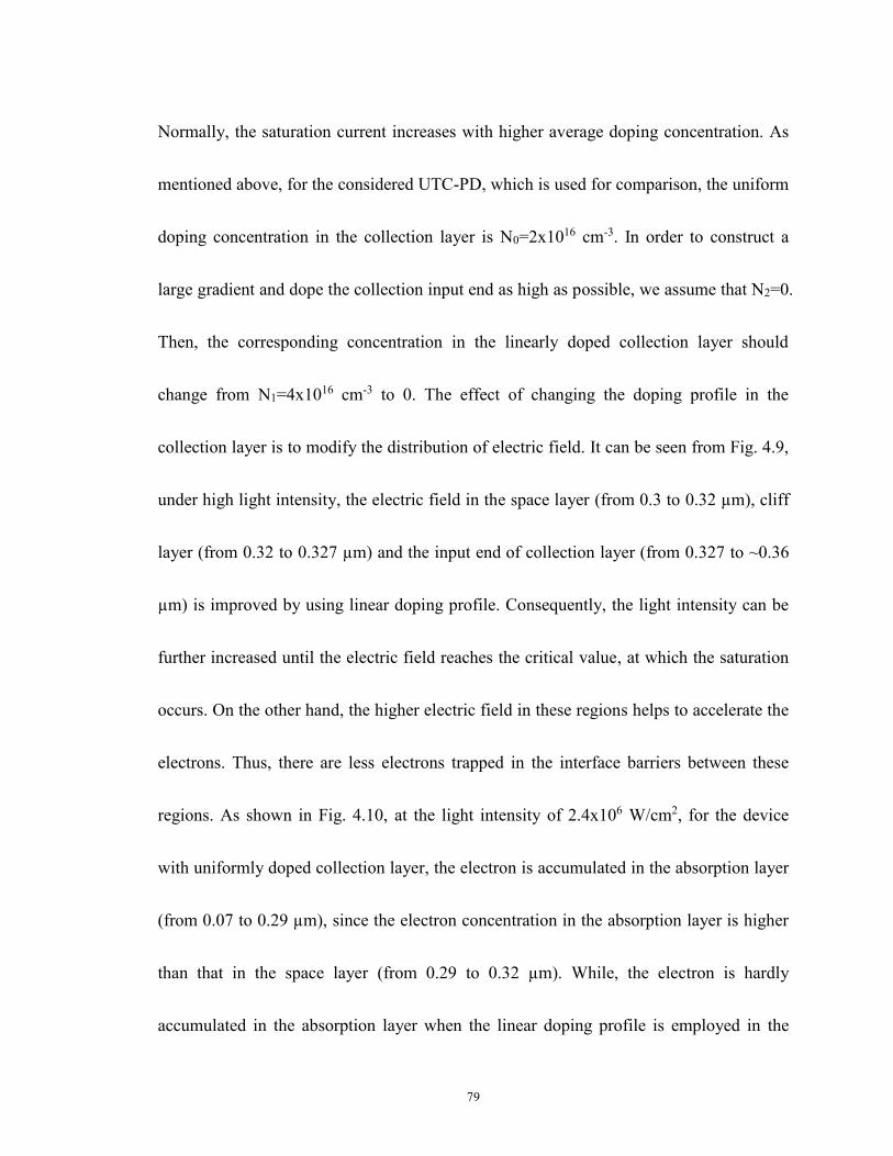
79
Normally, the saturation current increases with higher average doping concentration. As
mentioned above, for the considered UTC-PD, which is used for comparison, the uniform
doping concentration in the collection layer is N0=2x1016 cm-3. In order to construct a
large gradient and dope the collection input end as high as possible, we assume that N2=0.
Then, the corresponding concentration in the linearly doped collection layer should
change from N1=4x1016 cm-3 to 0. The effect of changing the doping profile in the
collection layer is to modify the distribution of electric field. It can be seen from Fig. 4.9,
under high light intensity, the electric field in the space layer (from 0.3 to 0.32 µm), cliff
layer (from 0.32 to 0.327 µm) and the input end of collection layer (from 0.327 to ~0.36
µm) is improved by using linear doping profile. Consequently, the light intensity can be
further increased until the electric field reaches the critical value, at which the saturation
occurs. On the other hand, the higher electric field in these regions helps to accelerate the
electrons. Thus, there are less electrons trapped in the interface barriers between these
regions. As shown in Fig. 4.10, at the light intensity of 2.4x10⁶ W/cm2, for the device
with uniformly doped collection layer, the electron is accumulated in the absorption layer
(from 0.07 to 0.29 µm), since the electron concentration in the absorption layer is higher
than that in the space layer (from 0.29 to 0.32 µm). While, the electron is hardly
accumulated in the absorption layer when the linear doping profile is employed in the
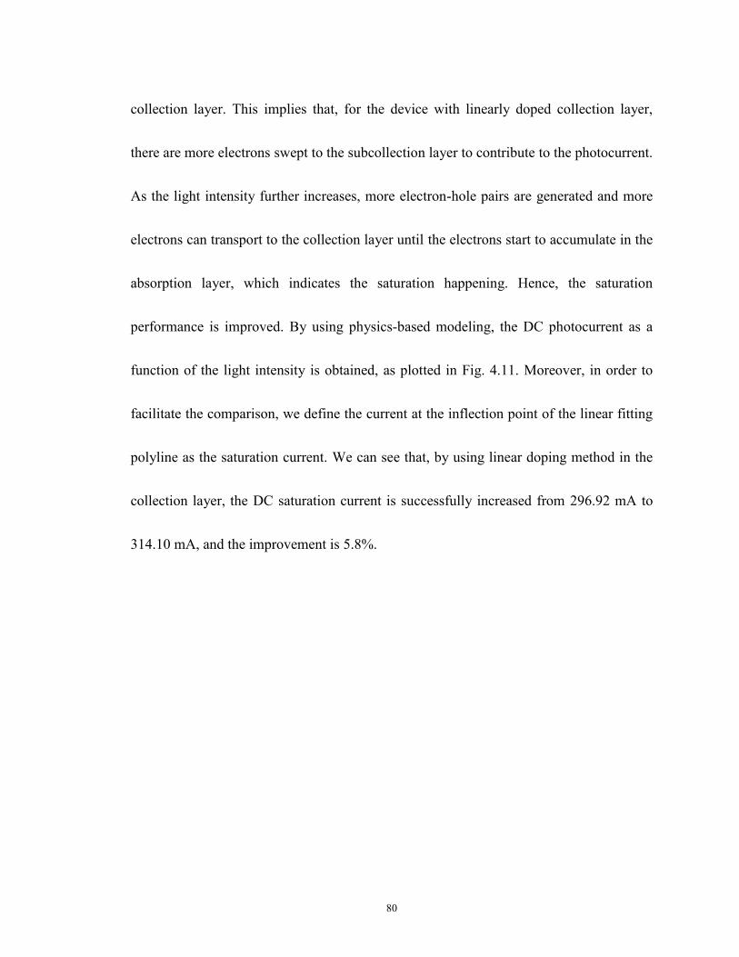
80
collection layer. This implies that, for the device with linearly doped collection layer,
there are more electrons swept to the subcollection layer to contribute to the photocurrent.
As the light intensity further increases, more electron-hole pairs are generated and more
electrons can transport to the collection layer until the electrons start to accumulate in the
absorption layer, which indicates the saturation happening. Hence, the saturation
performance is improved. By using physics-based modeling, the DC photocurrent as a
function of the light intensity is obtained, as plotted in Fig. 4.11. Moreover, in order to
facilitate the comparison, we define the current at the inflection point of the linear fitting
polyline as the saturation current. We can see that, by using linear doping method in the
collection layer, the DC saturation current is successfully increased from 296.92 mA to
314.10 mA, and the improvement is 5.8%.
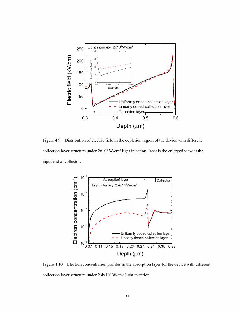
81
0.3 0.4 0.5 0.6
0
50
100
150
200
250
0.325 0.330 0.335 0.3400
10
20
30
40
Ele
cric
fie
ld (kV
/cm
)
Depth (m)
Light intensity: 2x10⁶W/cm
2
Uniformly doped collection layer
Linearly doped collection layer
Ele
cric fie
ld (
kV
/cm
)
Depth (m)
Collection layer
Figure 4.9 Distribution of electric field in the depletion region of the device with different
collection layer structure under 2x10⁶ W/cm2 light injection. Inset is the enlarged view at the
input end of collector.
0.07 0.11 0.15 0.19 0.23 0.27 0.31 0.35 0.3910
15
1016
1017
1018
1019
Light intensity: 2.4x10⁶W/cm
2
Uniformly doped collection layer
Linearly doped collection layer
Ele
ctr
on
co
nce
ntr
atio
n (
cm
-3)
Depth (m)
Absorption layer Collector
Figure 4.10 Electron concentration profiles in the absorption layer for the device with different
collection layer structure under 2.4x10⁶ W/cm2 light injection.
82
0 1 2 3 4 50.0
0.1
0.2
0.3
0.4
Uniformly doped collection layer
Linearly doped collection layer
Pho
tocu
rre
nt (A
)
Light intensity (106W/cm2)
Saturation current
Figure 4.11 Simulated DC photocurrent versus light intensity for the device with different
collection layer structure.
4.3.2 Optimization of linearly doped collection layer
As introduced previously, the saturation performance is mainly limited by the low
electric field in the collection layer near the absorption layer end under high optical levels.
The electric field near this end can be raised by increasing the doping concentration. Thus,
the saturation performance can be further improved by increasing the doping
concentration near this end. For the linear doping profile as we mentioned above, we
should increase the value of N1. However, if we only increase the value of N1 and do not
decrease the value of N2, the average doping concentration will become higher. Then, the
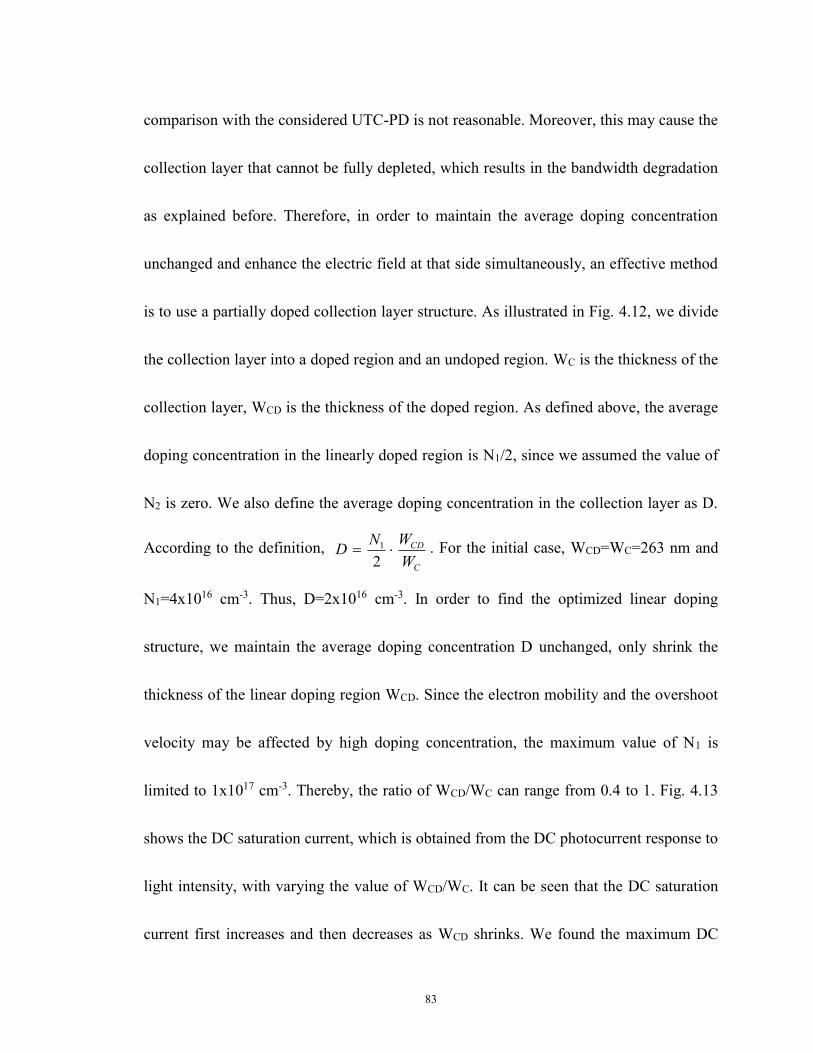
83
comparison with the considered UTC-PD is not reasonable. Moreover, this may cause the
collection layer that cannot be fully depleted, which results in the bandwidth degradation
as explained before. Therefore, in order to maintain the average doping concentration
unchanged and enhance the electric field at that side simultaneously, an effective method
is to use a partially doped collection layer structure. As illustrated in Fig. 4.12, we divide
the collection layer into a doped region and an undoped region. WC is the thickness of the
collection layer, WCD is the thickness of the doped region. As defined above, the average
doping concentration in the linearly doped region is N1/2, since we assumed the value of
N2 is zero. We also define the average doping concentration in the collection layer as D.
According to the definition, C
CD
W
WND
2
1 . For the initial case, WCD=WC=263 nm and
N1=4x1016 cm-3. Thus, D=2x1016 cm-3. In order to find the optimized linear doping
structure, we maintain the average doping concentration D unchanged, only shrink the
thickness of the linear doping region WCD. Since the electron mobility and the overshoot
velocity may be affected by high doping concentration, the maximum value of N1 is
limited to 1x1017 cm-3. Thereby, the ratio of WCD/WC can range from 0.4 to 1. Fig. 4.13
shows the DC saturation current, which is obtained from the DC photocurrent response to
light intensity, with varying the value of WCD/WC. It can be seen that the DC saturation
current first increases and then decreases as WCD shrinks. We found the maximum DC
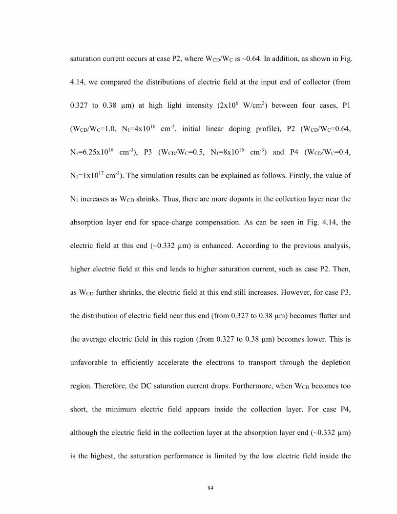
84
saturation current occurs at case P2, where WCD/WC is ~0.64. In addition, as shown in Fig.
4.14, we compared the distributions of electric field at the input end of collector (from
0.327 to 0.38 µm) at high light intensity (2x10⁶ W/cm2) between four cases, P1
(WCD/WC=1.0, N1=4x1016 cm-3, initial linear doping profile), P2 (WCD/WC=0.64,
N1=6.25x1016 cm-3), P3 (WCD/WC=0.5, N1=8x1016 cm-3) and P4 (WCD/WC=0.4,
N1=1x1017 cm-3). The simulation results can be explained as follows. Firstly, the value of
N1 increases as WCD shrinks. Thus, there are more dopants in the collection layer near the
absorption layer end for space-charge compensation. As can be seen in Fig. 4.14, the
electric field at this end (~0.332 µm) is enhanced. According to the previous analysis,
higher electric field at this end leads to higher saturation current, such as case P2. Then,
as WCD further shrinks, the electric field at this end still increases. However, for case P3,
the distribution of electric field near this end (from 0.327 to 0.38 µm) becomes flatter and
the average electric field in this region (from 0.327 to 0.38 µm) becomes lower. This is
unfavorable to efficiently accelerate the electrons to transport through the depletion
region. Therefore, the DC saturation current drops. Furthermore, when WCD becomes too
short, the minimum electric field appears inside the collection layer. For case P4,
although the electric field in the collection layer at the absorption layer end (~0.332 µm)
is the highest, the saturation performance is limited by the low electric field inside the
85
collection layer (~0.353 µm). Consequently, the saturation performance becomes even
worse. As can be seen from Fig. 4.13, for the considered UTC-PD, the optimal thickness
of linear doping region is ~168.3 µm (WCD/WC is ~0.64). After the optimization, the
improvement in DC saturation current, from P1 314.10 mA to P2 318.90 mA, is 1.53%,
which is not significant.
Figure 4.12 Schematic diagram of the linear doping profile optimization method. The left side
is the cliff layer side.
86
0.4 0.5 0.6 0.7 0.8 0.9 1.0312
313
314
315
316
317
318
319
320
P4
P3
P2
P1
DC
satu
ration c
urr
ent (m
A)
WCD/WC
Average doping concentration D: 2x10¹⁶
cm-3
Figure 4.13 Simulated DC saturation current versus WCD/WC at D=2x1016 cm-3.
0.33 0.34 0.35 0.36 0.37 0.3815
20
25
30
35
Ele
ctr
ic f
ield
(kV
/cm
)
Depth (m)
P1
P2
P3
P4
Light intensity: 2x10⁶W/cm
2
Figure 4.14 Distribution of electric field at the input end of collector under 2x10⁶ W/cm2 light
intensity for the four cases marked in Fig. 4.13.
87
4.4 Design of collection layer based on Gaussian doping profile
According to the previous analysis, the DC saturation current is not enhanced
significantly by the optimization of linearly doped collection layer. On the other hand, as
can be seen from Fig. 4.14, althought the maximum saturation current occurs at case P2,
its electric field in the collection layer near the absorption layer end (from 0.327 to ~0.34
µm) is lower than that of case P3. Thus, at high optical injection level, the minimum
electric field in the collection layer may not be the only factor that limits the saturation
performance. It is found that, the electric field gradient also has influence on the
saturation performance. When the minimum values of the electric field are similar, if the
electric field gradient at the input side of collection layer is larger, the saturation
performance will be better.
As mentioned above, near the input side of the collection layer, higher doping
concentration leads to higher electric field. While, for the output side of the collection
layer, the electric field decreases as the doping concentration increases. Thereby, in order
to enhance the electric field gradient near the collector input end and ensure a high
electric field near the output end, we need to first increase the doping concentration from
the collector input end and then decrease it from the peak value. This can be achieved by
88
using Gaussian doping profile. In the following, the design of collection layer based on
Gaussian doping profile is investigated.
In ATLAS, the Gaussian doping profile is given by [30]
2
Y.CHAR
PEAK-Y-expN.PEAK)(YN , (4.1)
where N.PEAK is the peak concentration of the Gaussian distribution, PEAK is the depth
location of the peak doping in the Gaussian profile, and Y.CHAR is the principal
characteristic length of the implant, which describes the spatial spread of the distribution.
Different Gaussian doping profiles can be obtained by changing these parameters.
Accordingly, different electric field distributions in the collection layer can be achieved.
We can optimize the saturation performance by adjusting N.PEAK, PEAK and Y.CHAR.
In addition, there is another condition that should be satisfied. In order to reasonably
compare with the considered UTC-PD, we should maintain the same average doping
concentration in the collection layer as mentioned above. Namely, the average doping
concentration in the collection layer should be 2x1016 cm-3. Here, we define the average
doping concentration D in the collection layer by CW
QD , where Q is the implant dose
contained within the collection layer, and WC is the thickness of the collection layer,
which is 263 nm for the studied UTC-PD. It can be calculated that, the implant dose Q in
89
the collection layer is 5.26x1011 cm-2. For Gaussian profile, the total dose can be
calculated by integrating N(Y) over the collection layer region, which can be expressed
as follows,
Y.CHARY.CHAR
yY.CHARN.PEAK
2
)(
12
2
1
PEAKyerf
PEAKerf
dYYNQy
y
(4.2)
where y1 and y2 are the depth location of the input side and output side of the collection
layer respectively. For the studied UTC-PD, y1=0.327 µm and y2=0.59 µm. According to
Eq. (4.2), for a given set of values of PEAK and Y.CHAR, a certain value of N.PEAK
can be obtained to satisfy the condition. Therefore, we only need to vary the values of
PEAK and Y.CHAR to find the suitable Gaussian doping profile, and thus achieve the
optimal saturation performance. The effects of these two parameters will be investigated.
Firstly, the impact of different locations of the peak doping concentration on the
saturation performance is studied. We assume the value of the principal characteristic
length Y.CHAR is 0.05 µm, and the location of the peak doping concentration PEAK
moves from the collector input end to the middle of the collection layer. When the peak
doping concentration of the Gaussian profile is at the input end of the collection layer, it
is similar to the case of linear doping profile. As shown in Table 4.1, the corresponding
peak concentration of the Gaussian distribution can be calculated by using Eq. (4.2).
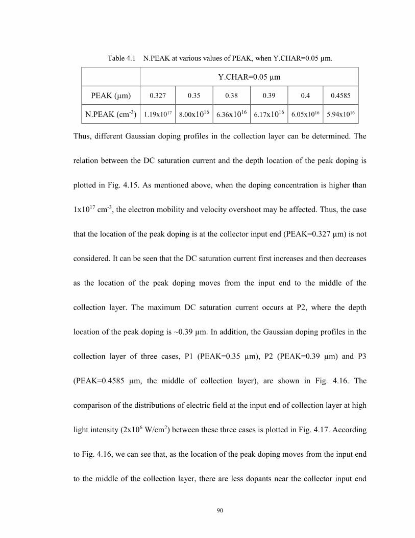
90
Table 4.1 N.PEAK at various values of PEAK, when Y.CHAR=0.05 µm.
Y.CHAR=0.05 µm
PEAK (µm) 0.327 0.35 0.38 0.39 0.4 0.4585
N.PEAK (cm-3) 1.19x10¹⁷ 8.00x10¹⁶ 6.36x10¹⁶ 6.17x10¹⁶ 6.05x10¹⁶ 5.94x10¹⁶
Thus, different Gaussian doping profiles in the collection layer can be determined. The
relation between the DC saturation current and the depth location of the peak doping is
plotted in Fig. 4.15. As mentioned above, when the doping concentration is higher than
1x1017 cm-3, the electron mobility and velocity overshoot may be affected. Thus, the case
that the location of the peak doping is at the collector input end (PEAK=0.327 µm) is not
considered. It can be seen that the DC saturation current first increases and then decreases
as the location of the peak doping moves from the input end to the middle of the
collection layer. The maximum DC saturation current occurs at P2, where the depth
location of the peak doping is ~0.39 µm. In addition, the Gaussian doping profiles in the
collection layer of three cases, P1 (PEAK=0.35 µm), P2 (PEAK=0.39 µm) and P3
(PEAK=0.4585 µm, the middle of collection layer), are shown in Fig. 4.16. The
comparison of the distributions of electric field at the input end of collection layer at high
light intensity (2x10⁶ W/cm2) between these three cases is plotted in Fig. 4.17. According
to Fig. 4.16, we can see that, as the location of the peak doping moves from the input end
to the middle of the collection layer, there are less dopants near the collector input end
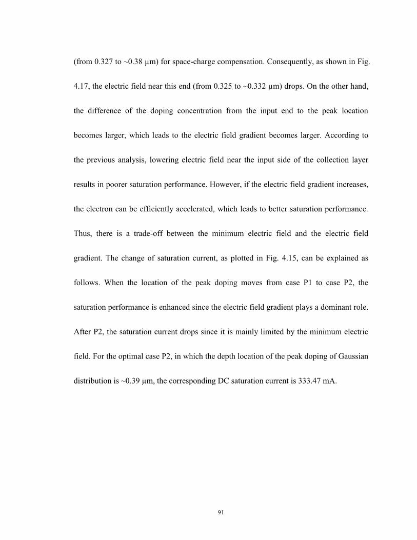
91
(from 0.327 to ~0.38 µm) for space-charge compensation. Consequently, as shown in Fig.
4.17, the electric field near this end (from 0.325 to ~0.332 µm) drops. On the other hand,
the difference of the doping concentration from the input end to the peak location
becomes larger, which leads to the electric field gradient becomes larger. According to
the previous analysis, lowering electric field near the input side of the collection layer
results in poorer saturation performance. However, if the electric field gradient increases,
the electron can be efficiently accelerated, which leads to better saturation performance.
Thus, there is a trade-off between the minimum electric field and the electric field
gradient. The change of saturation current, as plotted in Fig. 4.15, can be explained as
follows. When the location of the peak doping moves from case P1 to case P2, the
saturation performance is enhanced since the electric field gradient plays a dominant role.
After P2, the saturation current drops since it is mainly limited by the minimum electric
field. For the optimal case P2, in which the depth location of the peak doping of Gaussian
distribution is ~0.39 µm, the corresponding DC saturation current is 333.47 mA.
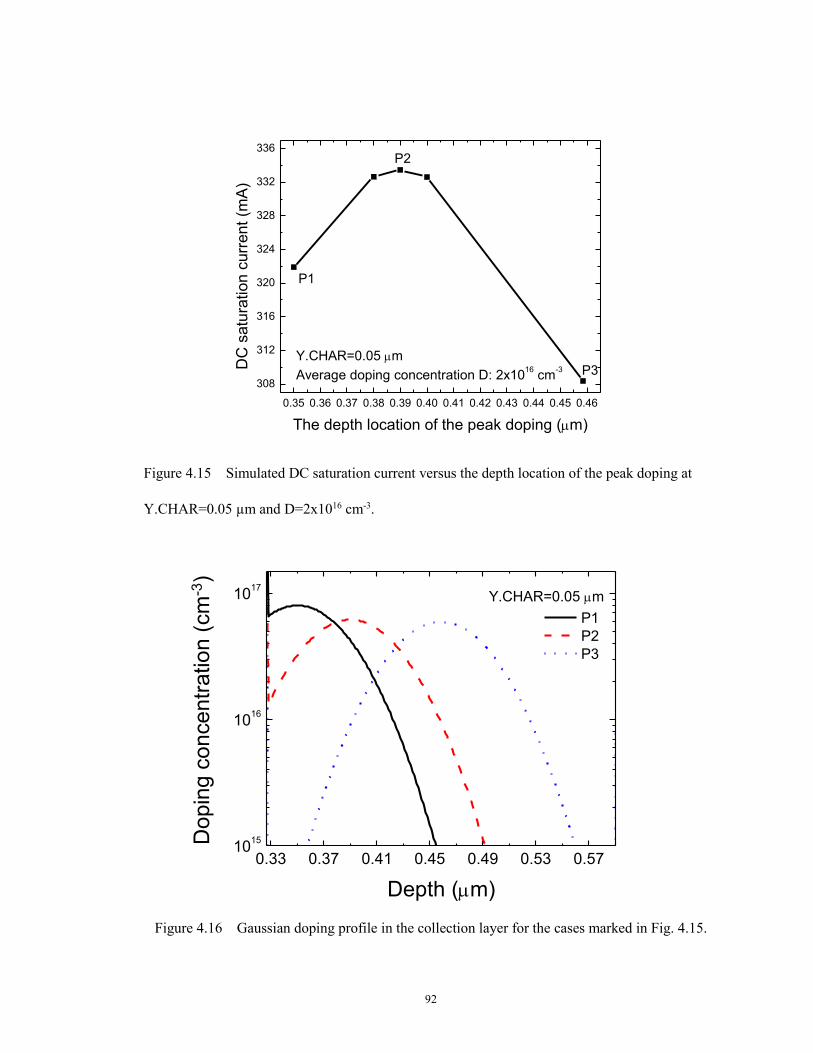
92
0.35 0.36 0.37 0.38 0.39 0.40 0.41 0.42 0.43 0.44 0.45 0.46
308
312
316
320
324
328
332
336
P1
P3
DC
satu
ration c
urr
ent
(mA
)
The depth location of the peak doping (m)
P2
Y.CHAR=0.05 m
Average doping concentration D: 2x10¹⁶
cm-3
Figure 4.15 Simulated DC saturation current versus the depth location of the peak doping at
Y.CHAR=0.05 µm and D=2x1016 cm-3.
0.33 0.37 0.41 0.45 0.49 0.53 0.5710
15
1016
1017
Do
pin
g c
on
ce
ntr
atio
n (
cm
-3)
Depth (m)
P1
P2
P3
Y.CHAR=0.05 m
Figure 4.16 Gaussian doping profile in the collection layer for the cases marked in Fig. 4.15.
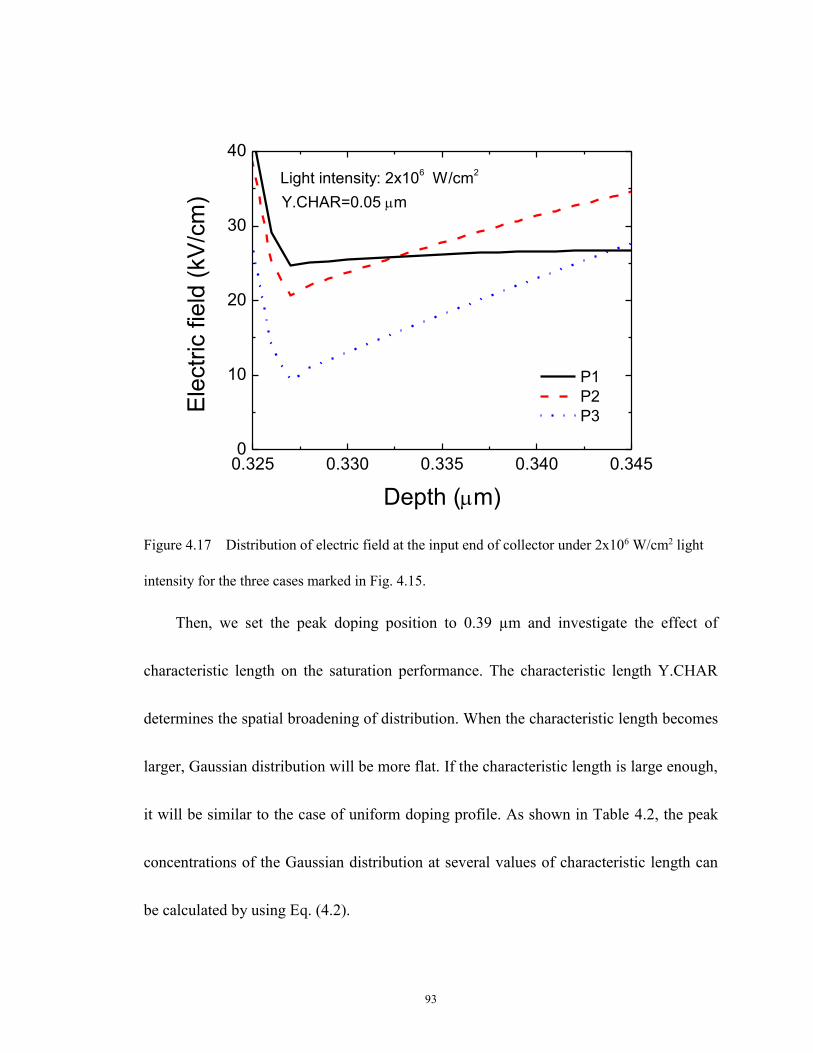
93
0.325 0.330 0.335 0.340 0.3450
10
20
30
40
P1
P2
P3
Y.CHAR=0.05 m
Ele
ctr
ic f
ield
(kV
/cm
)
Depth (m)
Light intensity: 2x10⁶ W/cm
2
Figure 4.17 Distribution of electric field at the input end of collector under 2x10⁶ W/cm2 light
intensity for the three cases marked in Fig. 4.15.
Then, we set the peak doping position to 0.39 µm and investigate the effect of
characteristic length on the saturation performance. The characteristic length Y.CHAR
determines the spatial broadening of distribution. When the characteristic length becomes
larger, Gaussian distribution will be more flat. If the characteristic length is large enough,
it will be similar to the case of uniform doping profile. As shown in Table 4.2, the peak
concentrations of the Gaussian distribution at several values of characteristic length can
be calculated by using Eq. (4.2).
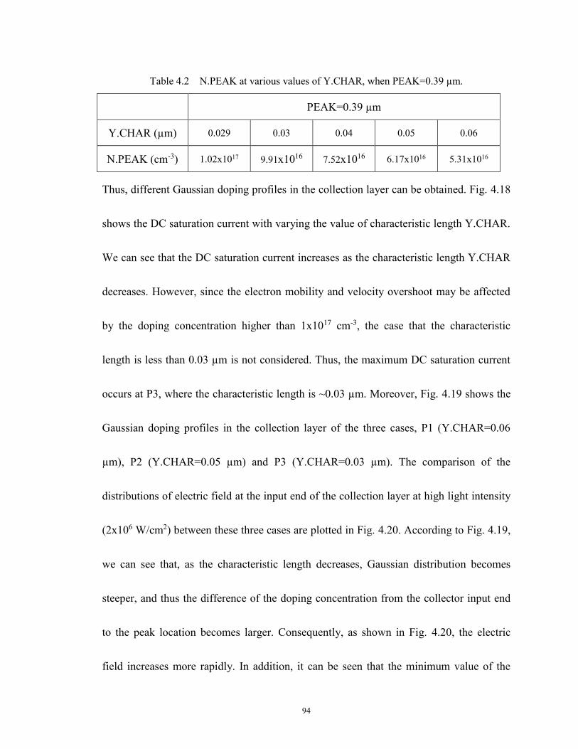
94
Table 4.2 N.PEAK at various values of Y.CHAR, when PEAK=0.39 µm.
PEAK=0.39 µm
Y.CHAR (µm) 0.029 0.03 0.04 0.05 0.06
N.PEAK (cm-3) 1.02x10¹⁷ 9.91x10¹⁶ 7.52x10¹⁶ 6.17x10¹⁶ 5.31x10¹⁶
Thus, different Gaussian doping profiles in the collection layer can be obtained. Fig. 4.18
shows the DC saturation current with varying the value of characteristic length Y.CHAR.
We can see that the DC saturation current increases as the characteristic length Y.CHAR
decreases. However, since the electron mobility and velocity overshoot may be affected
by the doping concentration higher than 1x1017 cm-3, the case that the characteristic
length is less than 0.03 µm is not considered. Thus, the maximum DC saturation current
occurs at P3, where the characteristic length is ~0.03 µm. Moreover, Fig. 4.19 shows the
Gaussian doping profiles in the collection layer of the three cases, P1 (Y.CHAR=0.06
µm), P2 (Y.CHAR=0.05 µm) and P3 (Y.CHAR=0.03 µm). The comparison of the
distributions of electric field at the input end of the collection layer at high light intensity
(2x10⁶ W/cm2) between these three cases are plotted in Fig. 4.20. According to Fig. 4.19,
we can see that, as the characteristic length decreases, Gaussian distribution becomes
steeper, and thus the difference of the doping concentration from the collector input end
to the peak location becomes larger. Consequently, as shown in Fig. 4.20, the electric
field increases more rapidly. In addition, it can be seen that the minimum value of the
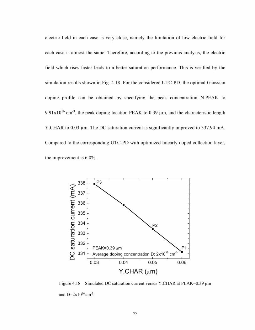
95
electric field in each case is very close, namely the limitation of low electric field for
each case is almost the same. Therefore, according to the previous analysis, the electric
field which rises faster leads to a better saturation performance. This is verified by the
simulation results shown in Fig. 4.18. For the considered UTC-PD, the optimal Gaussian
doping profile can be obtained by specifying the peak concentration N.PEAK to
9.91x1016 cm-3, the peak doping location PEAK to 0.39 µm, and the characteristic length
Y.CHAR to 0.03 µm. The DC saturation current is significantly improved to 337.94 mA.
Compared to the corresponding UTC-PD with optimized linearly doped collection layer,
the improvement is 6.0%.
0.03 0.04 0.05 0.06
331
332
333
334
335
336
337
338
P2
P3
PEAK=0.39 m
Average doping concentration D: 2x10¹⁶
cm-3
DC
sa
tura
tion
cu
rre
nt
(mA
)
Y.CHAR (m)
P1
Figure 4.18 Simulated DC saturation current versus Y.CHAR at PEAK=0.39 µm
and D=2x1016 cm-3.
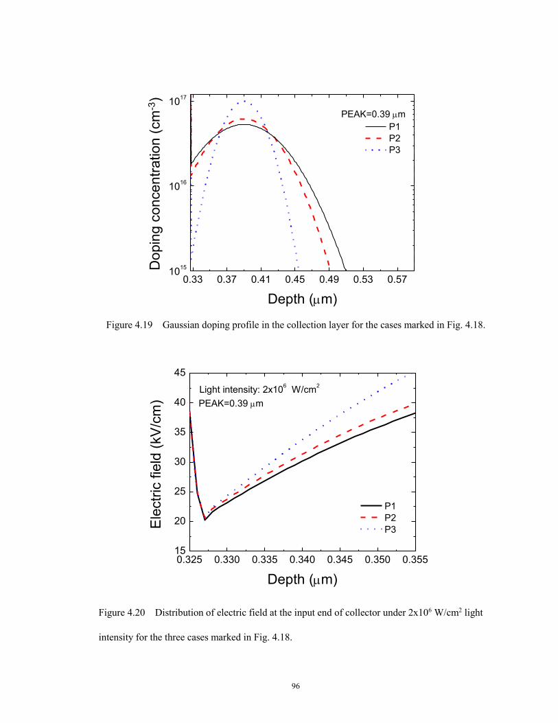
96
0.33 0.37 0.41 0.45 0.49 0.53 0.5710
15
1016
1017
Dopin
g c
oncentr
ation (
cm
-3)
Depth (m)
P1
P2
P3
PEAK=0.39 m
Figure 4.19 Gaussian doping profile in the collection layer for the cases marked in Fig. 4.18.
0.325 0.330 0.335 0.340 0.345 0.350 0.35515
20
25
30
35
40
45
Light intensity: 2x10⁶ W/cm
2
PEAK=0.39 m
Ele
ctr
ic fie
ld (
kV
/cm
)
Depth (m)
P1
P2
P3
Figure 4.20 Distribution of electric field at the input end of collector under 2x10⁶ W/cm2 light
intensity for the three cases marked in Fig. 4.18.
97
4.5 Discussion and summary
In this chapter, the doping effect in the collection layer is investigated. First of all, it
is verified that, as described in [54], the space-charge effect can be characterized by the
electric field reduction at the collector input under high current injection. And the
space-charge effect can be relieved by using the technique of charge compensation. It is
verified that the saturation current can be enhanced by employing a uniformly doped
collector layer. Then, in order to further improve the saturation perforance, a collection
layer with linear doping profile and a collection layer with Gaussian doping profile are
proposed. Moreover, all the methods are optimized. In the following, Fig. 4.21 shows the
different doping profiles in the collection layer, the corresponding distributions of electric
field near the input end of the collection layer are illustrated in Fig. 4.22, and the DC
photocurrent response to the optical source is plotted in Fig. 4.23. Firstly, according to
the optimization of uniform doping profile, it is found that, higher collector doping level
leads to better saturation performance. This is because the electric field in the space layer,
cliff layer and the collector input side is enhanced. However, 3-dB bandwidth drops at
high doping concentration, since the collection layer cannot be completely depleted at
normal device operation bias voltage. For PD80, the appropriate uniform doping

98
concentration is found to be 2x1016 cm-3. Compared to the original structure in [6], the
DC saturation current increases from 268.67 mA to 296.92 mA, an improvement of
10.5%. Then, the average doping concentration in the collection layer is maintained the
same, while the uniform doping profile is replaced by linear doping profile and Gaussian
doping profile. We can see that, the electric field is further enhanced, which further
reduces the space-charge effect, and thus leads to better saturation performance. By
employing the optimized linear doping profile, the saturation current can be increased to
318.90 mA. Compared to the original structure [6], the improvement is 18.7%. While, a
saturation current of 337.94 mA is achieved by using optimized Gaussian doping profile.
Compared to the original structure [6], the improvement is 25.8%. As can be seen from
Fig. 4.22, comparing the Gaussian doping method with the linear doping method,
although the electric field in the space layer (from 0.31 to 0.32 µm), cliff layer (from 0.32
to 0.327 µm) and the collector input end (from 0.327 to ~0.329 µm) is a little bit lower,
the rapidly rising electric field in the collection layer leads to the better saturation
performance.
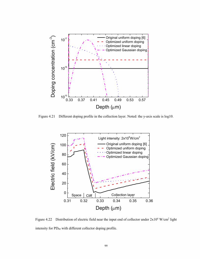
99
0.33 0.37 0.41 0.45 0.49 0.53 0.5710
15
1016
1017
Do
pin
g c
on
ce
ntr
atio
n (
cm
-3)
Depth (m)
Original uniform doping [6]
Optimized uniform doping
Optimized linear doping
Optimized Gaussian doping
Figure 4.21 Different doping profile in the collection layer. Noted: the y-axis scale is log10.
0.31 0.32 0.33 0.34 0.35 0.36
0
20
40
60
80
100
120Light intensity: 2x10
6W/cm
2
Ele
ctr
ic fie
ld (
kV
/cm
)
Depth (m)
Original uniform doping [6]
Optimized uniform doping
Optimized linear doping
Optimized Gaussian doping
Space Cliff Collection layer
Figure 4.22 Distribution of electric field near the input end of collector under 2x10⁶ W/cm2 light
intensity for PD80 with different collector doping profile.
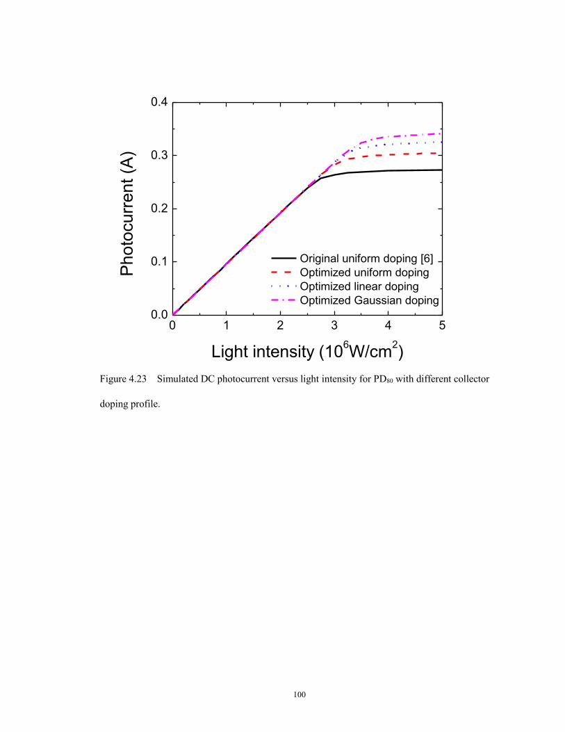
100
0 1 2 3 4 50.0
0.1
0.2
0.3
0.4
Pho
tocurr
ent (A
)
Light intensity (106W/cm
2)
Original uniform doping [6]
Optimized uniform doping
Optimized linear doping
Optimized Gaussian doping
Figure 4.23 Simulated DC photocurrent versus light intensity for PD80 with different collector
doping profile.
101
Chapter 5 Design and Fabrication of High-Speed and
High-Power UTC-PDs
As described in chapter 3, we proposed a novel graded bandgap absorption layer
structure to improve the speed performance. In this chapter, the epitaxial layer structures
of two designed broadband and high-output power UTC-PDs are described. Different
from the first UTC-PD (PDA), the other UTC-PD (PDB) employs a graded bandgap
absorption layer to enhance the bandwidth performance. Moreover, a cliff layer, which
can be used to improve saturation performance, is added in PDB. Additionally, the design
of fabrication process is introduced.
5.1 Device structure
The epitaxial layer structure of PDA is designed according to the Near-ballistic
UTC-PD (NBUTC-PD) reported by J.-W. Shi et al. [19]. Their NBUTC-PD shows
superior performance. A 250 GHz bandwidth and a 17 mA saturation current under a 50
ohm load has been demonstrated [19]. Both the structures of PDA and PDB were grown
on semi-insulating (S.I.) InP substrates by the chemical beam epitaxy (CBE) reactor.
Table. 5.1 shows the epitaxial layer structure of our designed PDA in detail. Compared
with their NBUTC-PD, the major difference is that we employ In1-xGaxAsyP1-y system
102
instead of In1-x-yAlxGayAs system. Starting from the substrate, the epitaxial layer growth
begins sequentially with a 200 nm n+ InP layer and a 20 nm n+ In0.53Ga0.47As etching stop
layer. The 800 nm n+ InP contact layer is highly doped to 4x1018 cm-3 to reduce the
contact resistance. Followed is three thin charge layers, which consist of a 5 nm n+ InP
charge layer, a 5 nm p− InP charge layer and a 10 nm p+ InP charge layer. Charge layers
are inserted to control the distribution of the electric field in the collector layer. Then, the
120 nm n− InP collection layer is followed by a 20 nm lightly n-type doped
In0.53Ga0.47As→InP transition layer. As mentioned in chapter 4, the collection layer is
n-type doped to 2x1016 cm−3 for charge compensation. The transition layer is employed to
form a smooth connection between the absorption layer and the collection layer. Here,
the transition layer is achieved by changing the the composition fractions x and y of
In1-xGaxAsyP1-y. The composition fraction x varies linearly from 0.47 to 0, and y varies
from 1 to 0 correspondingly. The 150 nm p-type In0.53Ga0.47As absorption layer employs
a linearly graded doping profile to introduce a built-in electric field which can assist
electron to transport. The highest doping concentration in the absorption layer is located
at the blocking layer side and the lowest concentration is located at the transition layer
side. Above the absorption layer, the function of the 80 nm wide bandgap p+ InP blocking
layer is to prevent the diffusion of the electrons to the anode and promote the electrons
103
generated in the absorption layer to transport towards the InP collection layer. On top is a
100 nm p+ In0.53Ga0.47As contact layer, which is highly doped to form a good ohmic
contact. The epitaxial layer structure of PDB is shown in Table. 5.2. Compared to PDA, a
graded bandgap absorption layer is employed in PDB to construct a built-in electric field
and thus improve the speed performance. The In0.53Ga0.47As absorption layer of PDA is
replaced by a linear compositionally-graded In0.59Ga0.41As0.88P0.16→In0.53Ga0.47As
absorption layer. As a result, for PDB, the energy gap of the absorption layer varies
linearly from 0.786 eV to 0.737 eV. This linearly graded energy gap is suitable for the
device operation at a optical wavelength of 1.55 μm, and can introduce a built-in electric
field to accelerate the electrons. It is noted that, similar to the NBUTC-PD structure in
[19], for both PDA and PDB, the charge layer is inserted between the collection layer and
the n-contact layer. The charge layer is used to enhance the electric field near the output
side of the collection layer. In addition, for PDB, not only the charge layer, but also a 20
nm n+ InP cliff layer is added between the transition layer and the collection layer. The
function of the cliff layer is similar to that of the charge layer. It is used to sustain the
high electric field near the input side of the collection layer. And thus the saturation
performance can be further enhanced.
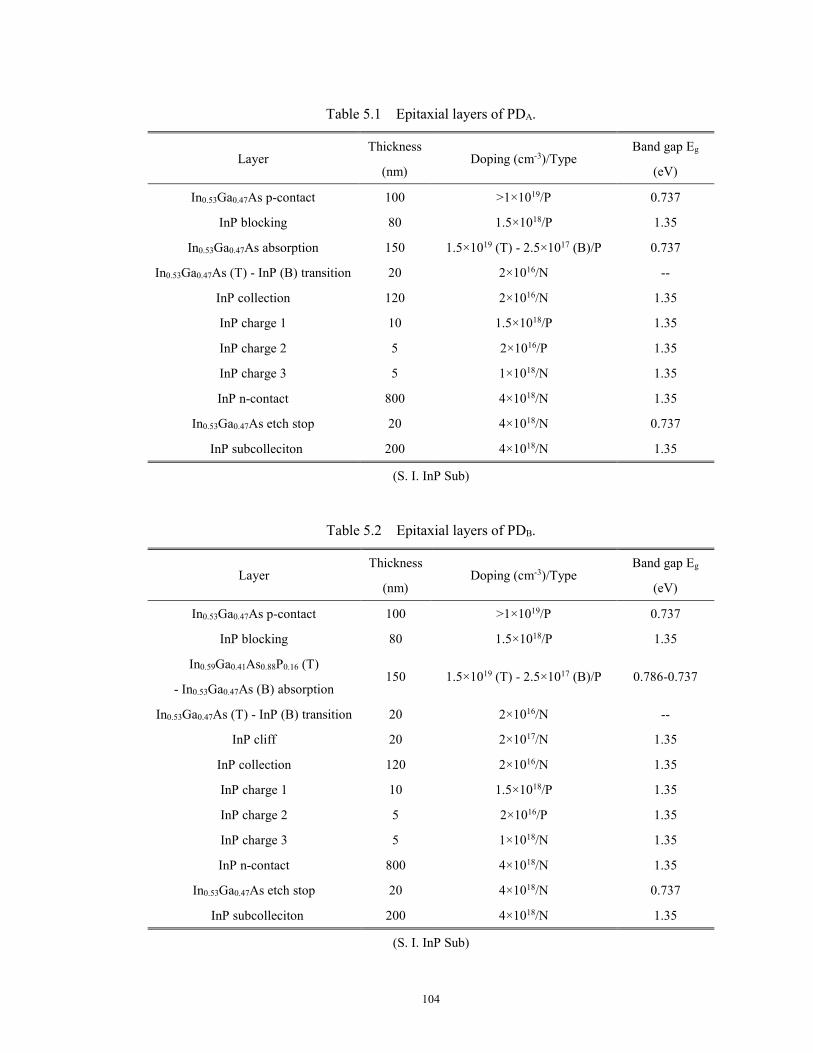
104
Table 5.1 Epitaxial layers of PDA.
Layer Thickness
(nm) Doping (cm-3)/Type
Band gap Eg
(eV)
In0.53Ga0.47As p-contact 100 >1×10¹⁹/P 0.737
InP blocking 80 1.5×10¹⁸/P 1.35
In0.53Ga0.47As absorption 150 1.5×10¹⁹ (T) - 2.5×10¹⁷ (B)/P 0.737
In0.53Ga0.47As (T) - InP (B) transition 20 2×10¹⁶/N --
InP collection 120 2×10¹⁶/N 1.35
InP charge 1 10 1.5×10¹⁸/P 1.35
InP charge 2 5 2×10¹⁶/P 1.35
InP charge 3 5 1×10¹⁸/N 1.35
InP n-contact 800 4×10¹⁸/N 1.35
In0.53Ga0.47As etch stop 20 4×10¹⁸/N 0.737
InP subcolleciton 200 4×10¹⁸/N 1.35
(S. I. InP Sub)
Table 5.2 Epitaxial layers of PDB.
Layer Thickness
(nm) Doping (cm-3)/Type
Band gap Eg
(eV)
In0.53Ga0.47As p-contact 100 >1×10¹⁹/P 0.737
InP blocking 80 1.5×10¹⁸/P 1.35
In0.59Ga0.41As0.88P0.16 (T)
- In0.53Ga0.47As (B) absorption 150 1.5×10¹⁹ (T) - 2.5×10¹⁷ (B)/P 0.786-0.737
In0.53Ga0.47As (T) - InP (B) transition 20 2×10¹⁶/N --
InP cliff 20 2×10¹⁷/N 1.35
InP collection 120 2×10¹⁶/N 1.35
InP charge 1 10 1.5×10¹⁸/P 1.35
InP charge 2 5 2×10¹⁶/P 1.35
InP charge 3 5 1×10¹⁸/N 1.35
InP n-contact 800 4×10¹⁸/N 1.35
In0.53Ga0.47As etch stop 20 4×10¹⁸/N 0.737
InP subcolleciton 200 4×10¹⁸/N 1.35
(S. I. InP Sub)
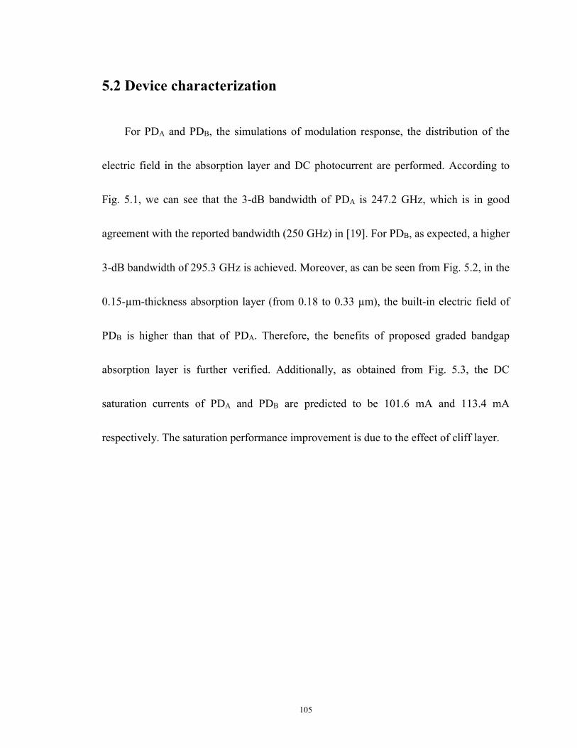
105
5.2 Device characterization
For PDA and PDB, the simulations of modulation response, the distribution of the
electric field in the absorption layer and DC photocurrent are performed. According to
Fig. 5.1, we can see that the 3-dB bandwidth of PDA is 247.2 GHz, which is in good
agreement with the reported bandwidth (250 GHz) in [19]. For PDB, as expected, a higher
3-dB bandwidth of 295.3 GHz is achieved. Moreover, as can be seen from Fig. 5.2, in the
0.15-µm-thickness absorption layer (from 0.18 to 0.33 µm), the built-in electric field of
PDB is higher than that of PDA. Therefore, the benefits of proposed graded bandgap
absorption layer is further verified. Additionally, as obtained from Fig. 5.3, the DC
saturation currents of PDA and PDB are predicted to be 101.6 mA and 113.4 mA
respectively. The saturation performance improvement is due to the effect of cliff layer.
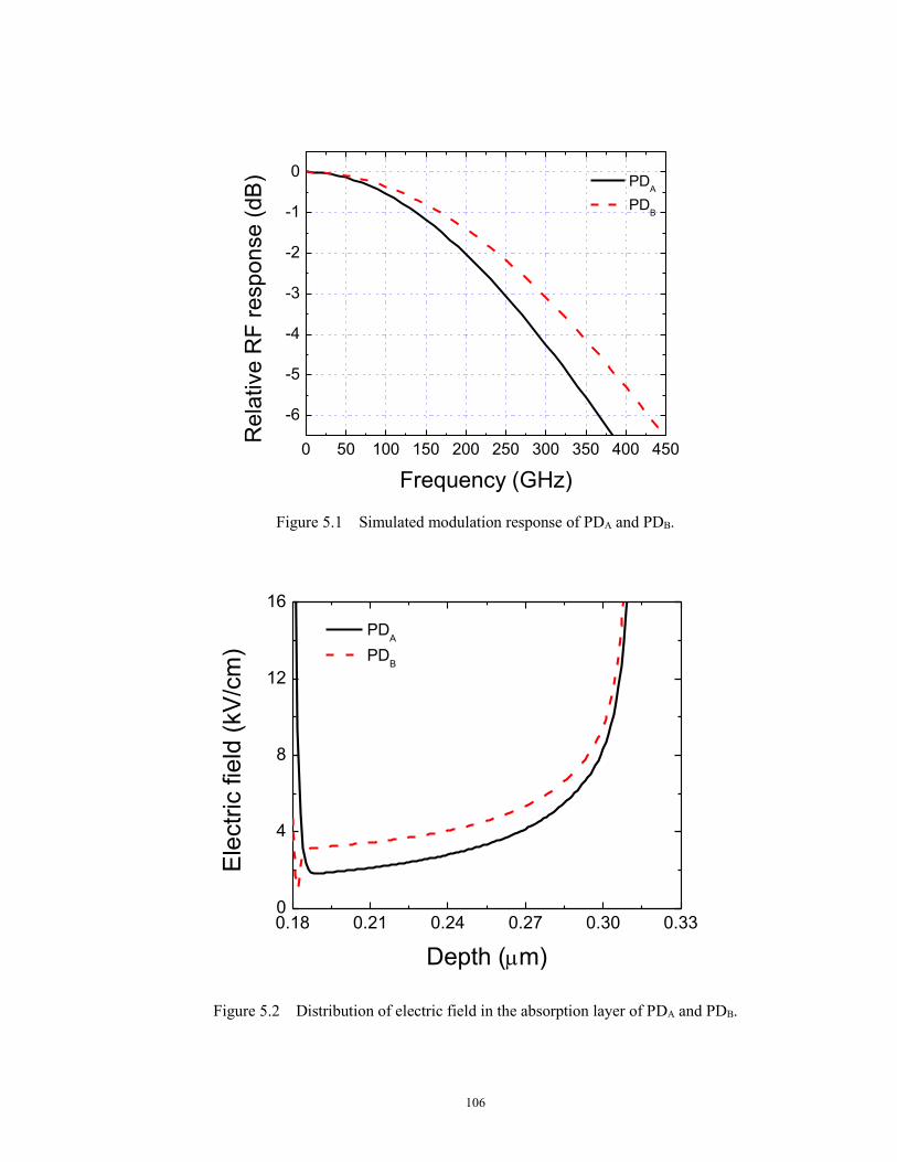
106
0 50 100 150 200 250 300 350 400 450
-6
-5
-4
-3
-2
-1
0
Re
lative
RF
resp
on
se
(dB
)
Frequency (GHz)
PDA
PDB
Figure 5.1 Simulated modulation response of PDA and PDB.
0.18 0.21 0.24 0.27 0.30 0.330
4
8
12
16
Ele
ctr
ic fie
ld (
kV
/cm
)
Depth (m)
PDA
PDB
Figure 5.2 Distribution of electric field in the absorption layer of PDA and PDB.
107
0 2 4 6 8 10 120
20
40
60
80
100
120
Pho
tocurr
ent (m
A)
Light intensity (106W/cm
2)
PDA
PDB
Figure 5.3 Simulated DC photocurrent versus light intensity of PDA and PDB.
5.3 Device fabrication
This section describes the design of fabrication process of the above mentioned
UTC-PD PDA and PDB. In order to save time and to avoid device failure which may be
caused by fabrication process, we need to minimize process steps and reduce process
complexity as far as possible. Thus, we will fabricate the wafer into backside illuminated
mesa structures by using conventional photolithography, dry and wet etching, passivation,
and metal liftoff techniques. In the following, the important techniques and the major
steps of fabrication flow will be described in sequence.
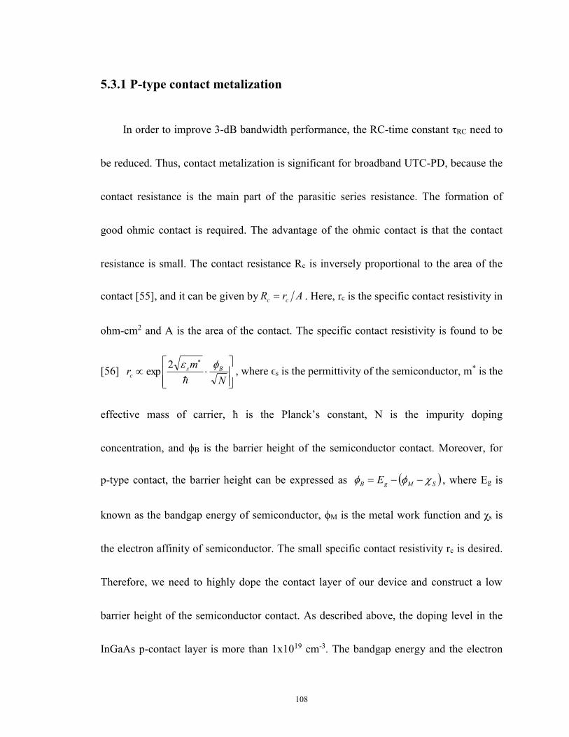
108
5.3.1 P-type contact metalization
In order to improve 3-dB bandwidth performance, the RC-time constant τRC need to
be reduced. Thus, contact metalization is significant for broadband UTC-PD, because the
contact resistance is the main part of the parasitic series resistance. The formation of
good ohmic contact is required. The advantage of the ohmic contact is that the contact
resistance is small. The contact resistance Rc is inversely proportional to the area of the
contact [55], and it can be given by ArR cc . Here, rc is the specific contact resistivity in
ohm-cm2 and A is the area of the contact. The specific contact resistivity is found to be
[56]
N
mr Bsc
2exp , where ϵs is the permittivity of the semiconductor, m* is the
effective mass of carrier, ħ is the Planck’s constant, N is the impurity doping
concentration, and ϕB is the barrier height of the semiconductor contact. Moreover, for
p-type contact, the barrier height can be expressed as SMgB E , where Eg is
known as the bandgap energy of semiconductor, ϕM is the metal work function and χs is
the electron affinity of semiconductor. The small specific contact resistivity rc is desired.
Therefore, we need to highly dope the contact layer of our device and construct a low
barrier height of the semiconductor contact. As described above, the doping level in the
InGaAs p-contact layer is more than 1x1019 cm-3. The bandgap energy and the electron
109
affinity of InGaAs is 0.737 eV and 4.58 eV respectively. We use Au (gold, ϕM=5.1 eV) as
the contact metal, since Au leads to a low barrier height and it has good electrical
conductivity. However, Au may diffuse into semiconductor. The diffusion leads to the
formation of spikes of Au, which may penetrate the contact region. To solve the spiking
problem, we use Pt (platinum, ϕM=5.65 eV) as a barrier to prevent spiking. In addition, Ti
(titanium, ϕM=4.33 eV) is added to provide good adhesion to the InGaAs p-contact layer.
The p-type contact metalization process starts from the wafer cleaning. Then, the
lift-off resist (LOR), which is used for the liftoff process, can be deposited immediately.
Followed by depositing a layer of photoresist. Thereby, the p-type contact metal window
can be opened by using the corresponding mask after the photoresist exposure and
development. Subsequently, in order to improve the ohmic contact, we need to remove
the oxide over the surface. Then, as mentioned above, the metal sequence Ti/Pt/Au
(30/50/300 nm) can be deposited by electron-beam evaporation. Finally, the wafer need
to be immersed in acetone to dissolve the LOR. Thus, all the materials deposited above
the LOR will be removed simultaneously, only leaving the patterned p-type contact metal
on the top of the wafer. The schematic diagram of the wafer after p-type contact
metalization is illustrated in Fig. 5.4(a). And Fig. 5.4(b) shows the corresponding
cross-sectional view.
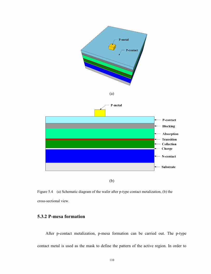
110
(a)
(b)
Figure 5.4 (a) Schematic diagram of the wafer after p-type contact metalization, (b) the
cross-sectional view.
5.3.2 P-mesa formation
After p-contact metalization, p-mesa formation can be carried out. The p-type
contact metal is used as the mask to define the pattern of the active region. In order to
111
avoid affecting the performance of the device and to minimize the dimension changes in
vertical direction, reactive-ion etching (RIE) technology is used to expose the heavily
doped n-type InP contact layer. The etching depth is about 0.5 µm. The drawback of dry
etching process is that it may cause damage to the sidewalls of p-mesa, which results in
the surface leakage current. Thus, after etching, we can dip the wafer in Br-methanol
etchant for seconds to remove the damaged portion on the surface of the sidewalls. Then,
as shown in Fig. 5.5(a), p-mesa, namely the active region is formed. Its cross-sectional
view is also illustrated in Fig. 5.5(b).
(a)
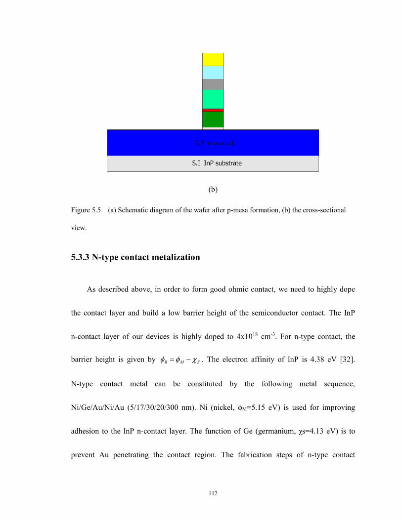
112
(b)
Figure 5.5 (a) Schematic diagram of the wafer after p-mesa formation, (b) the cross-sectional
view.
5.3.3 N-type contact metalization
As described above, in order to form good ohmic contact, we need to highly dope
the contact layer and build a low barrier height of the semiconductor contact. The InP
n-contact layer of our devices is highly doped to 4x1018 cm-3. For n-type contact, the
barrier height is given by SMB . The electron affinity of InP is 4.38 eV [32].
N-type contact metal can be constituted by the following metal sequence,
Ni/Ge/Au/Ni/Au (5/17/30/20/300 nm). Ni (nickel, ϕM=5.15 eV) is used for improving
adhesion to the InP n-contact layer. The function of Ge (germanium, χs=4.13 eV) is to
prevent Au penetrating the contact region. The fabrication steps of n-type contact
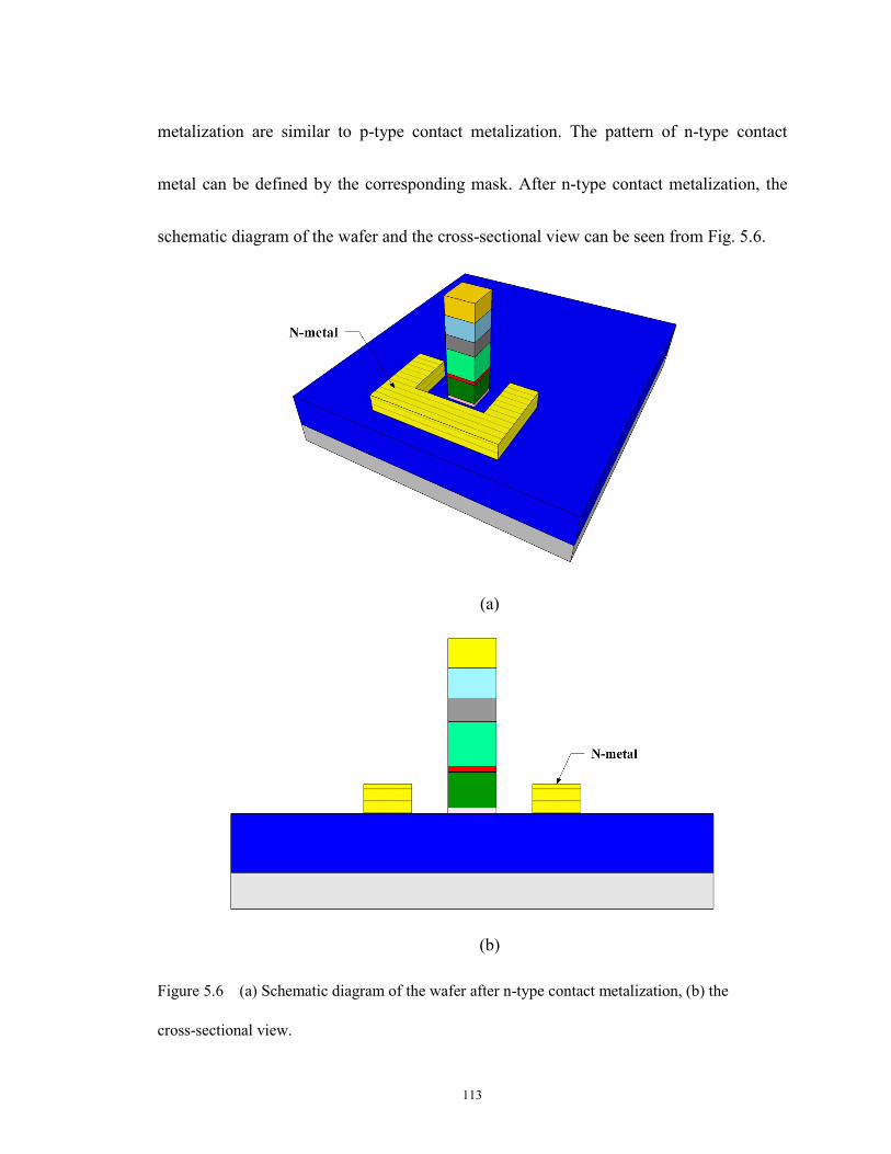
113
metalization are similar to p-type contact metalization. The pattern of n-type contact
metal can be defined by the corresponding mask. After n-type contact metalization, the
schematic diagram of the wafer and the cross-sectional view can be seen from Fig. 5.6.
(a)
(b)
Figure 5.6 (a) Schematic diagram of the wafer after n-type contact metalization, (b) the
cross-sectional view.

114
5.3.4 N-mesa formation
In order to make isolation between devices, and lower the parasitic effects such as
the parasitic capacitance, n-mesa etching is required. Prior to etching, the surface of the
wafer need to be coated with photoresist. Since there is about 0.5 µm height difference on
the surface of the wafer after the p-mesa formation, we need a thick coating of photoresist.
After photoresist exposure and development, the pattern of n-mesa region is transferred
from the corresponding mask to the surface of the wafer. For n-mesa formation, wet
etching is suitable to remove the excess n-contact layer and expose the semi-insulating
substrate. After etching, the wafer need to be immersed in acetone to remove all the
photoresist. Fig. 5.7(a) is the schematic diagram of the wafer after n-mesa formation. The
cross-sectional view is shown in Fig. 5.7(b).
(a)
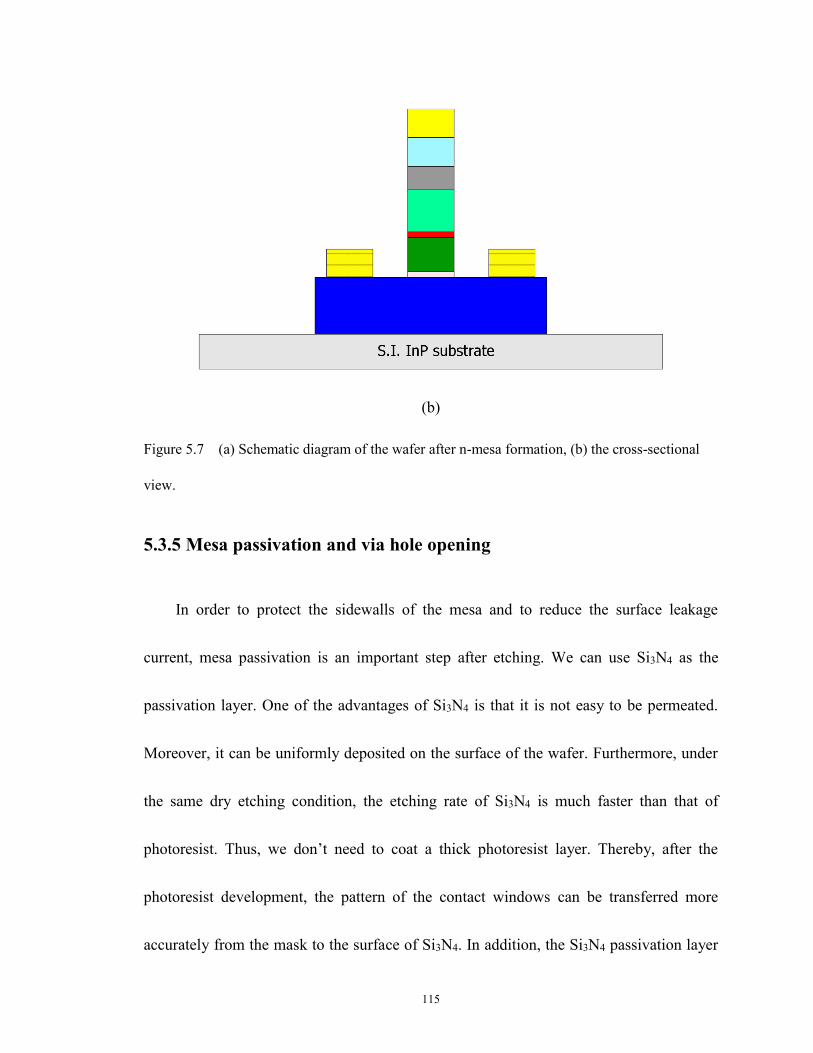
115
(b)
Figure 5.7 (a) Schematic diagram of the wafer after n-mesa formation, (b) the cross-sectional
view.
5.3.5 Mesa passivation and via hole opening
In order to protect the sidewalls of the mesa and to reduce the surface leakage
current, mesa passivation is an important step after etching. We can use Si3N4 as the
passivation layer. One of the advantages of Si3N4 is that it is not easy to be permeated.
Moreover, it can be uniformly deposited on the surface of the wafer. Furthermore, under
the same dry etching condition, the etching rate of Si3N4 is much faster than that of
photoresist. Thus, we don’t need to coat a thick photoresist layer. Thereby, after the
photoresist development, the pattern of the contact windows can be transferred more
accurately from the mask to the surface of Si3N4. In addition, the Si3N4 passivation layer
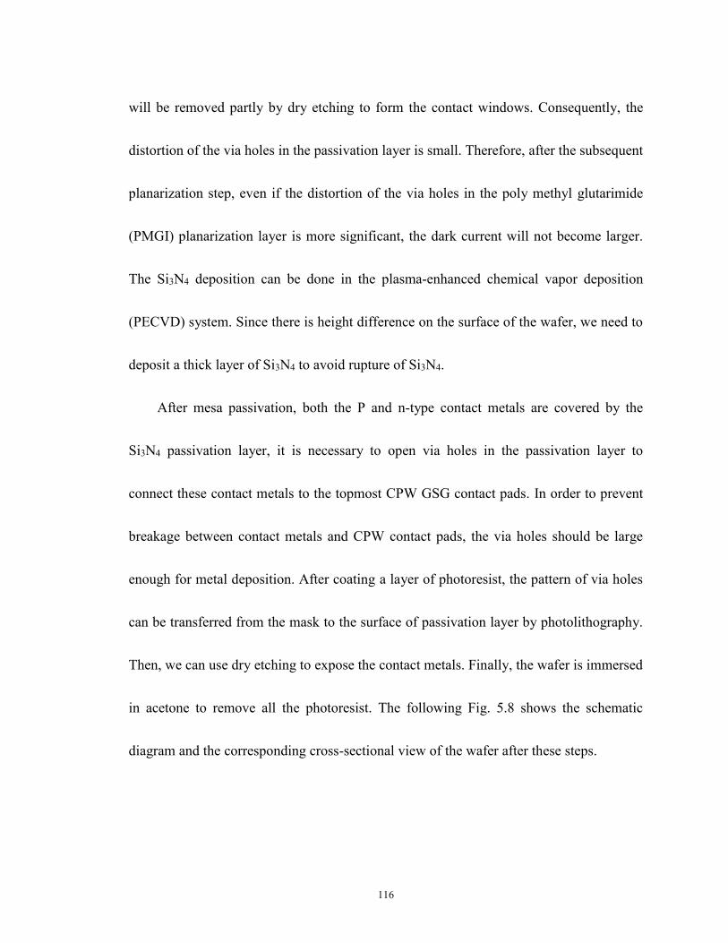
116
will be removed partly by dry etching to form the contact windows. Consequently, the
distortion of the via holes in the passivation layer is small. Therefore, after the subsequent
planarization step, even if the distortion of the via holes in the poly methyl glutarimide
(PMGI) planarization layer is more significant, the dark current will not become larger.
The Si3N4 deposition can be done in the plasma-enhanced chemical vapor deposition
(PECVD) system. Since there is height difference on the surface of the wafer, we need to
deposit a thick layer of Si3N4 to avoid rupture of Si3N4.
After mesa passivation, both the P and n-type contact metals are covered by the
Si3N4 passivation layer, it is necessary to open via holes in the passivation layer to
connect these contact metals to the topmost CPW GSG contact pads. In order to prevent
breakage between contact metals and CPW contact pads, the via holes should be large
enough for metal deposition. After coating a layer of photoresist, the pattern of via holes
can be transferred from the mask to the surface of passivation layer by photolithography.
Then, we can use dry etching to expose the contact metals. Finally, the wafer is immersed
in acetone to remove all the photoresist. The following Fig. 5.8 shows the schematic
diagram and the corresponding cross-sectional view of the wafer after these steps.
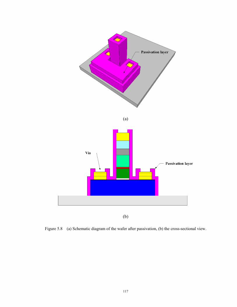
117
(a)
(b)
Figure 5.8 (a) Schematic diagram of the wafer after passivation, (b) the cross-sectional view.
118
5.3.6 Planarization and via hole opening
After the above steps, height difference still exists on the surface of the wafer.
Taking into account the deposition of the topmost CPW-like GSG contact pads and the
simplification of the fabrication process, we need to create a flat surface. In this way, we
can directly deposit the GSG contact pads on the top of the wafer, and thus the following
lithography step will be much easier. PMGI can be employed to achieve the highly planar
layer, because it has several advantages as follows. First of all, the dielectric constant of
PMGI is low, and thus the parasitic capacitance is small. Moreover, the performance of
CPW contact pads can be improved by using a substrate with low dielectric constant. In
addition, PMGI has a characteristic of reflow. Namely, when the temperature exceeds the
critical temperature, the solid PMGI will liquefy. Because of this feature, PMGI is
preferable to benzocyclobutene (BCB) to form the planarization layer. In order to cover
the surface of the wafer, where exists a height difference of a few microns, we need to
deposit a thick planarization layer. Then, similar to the passivation layer, via holes need
to be opened in the planarization layer to make connections between the contact metals
and the topmost CPW GSG contact pads. If BCB is used for planarization, after the
opening of the via holes by dry etching, the sidewalls will be too steep, almost vertical.
119
This may result in breakage in the subsequently deposited metal in the via hole. Thus,
there may be disconnection between the contact metals and the GSG contact pads. This
problem can be solved by using PMGI to form the planarization layer. Due to the
characteristic of reflow, if the temperature and time are controlled appropriately, a
smooth tapered sidewall can be formed, which facilitates the deposition of metal.
Accordingly, the breakage between contact metals and GSG contact pads can be avoided.
Similar to the mesa passivation step, when there is sufficient PMGI coated on the
surface of the wafer to form a highly planar layer, the opening of via hole is required.
Moreover, the process steps of the definition of the pattern of via holes are the same as
those of mesa passivation. However, as mentioned above, we need to pay attention to the
distortion problem. Since both the PMGI and photoresist belong to the polymer, under
the same dry etching condition, the etching rate of PMGI is similar to that of photoresist.
Thus, we need to use a thick photoresist layer as the barrier. The problem of the thick
photoresist layer is that it may be overdeveloped, which results in the actual opening of
the via hole is too large. Particularly, for the small devices, the size of the via hole
opening is very important. On the one hand, in order to prevent breakage between contact
metals and CPW contact pads, the opening should be large enough so that the metal
deposition is facilitated. On the other hand, the opening should not be too large. It is
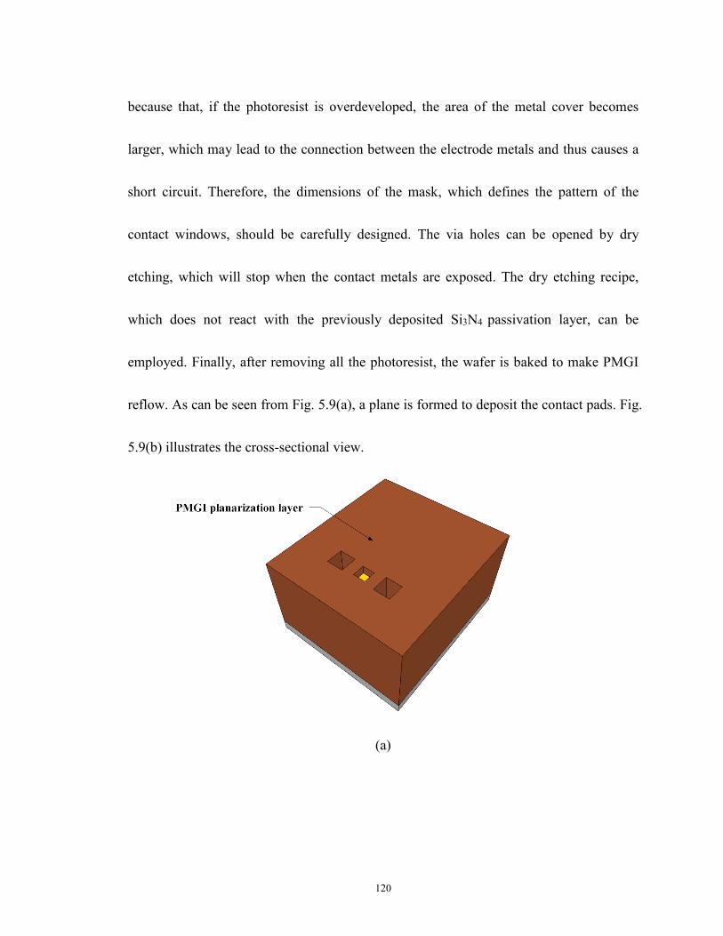
120
because that, if the photoresist is overdeveloped, the area of the metal cover becomes
larger, which may lead to the connection between the electrode metals and thus causes a
short circuit. Therefore, the dimensions of the mask, which defines the pattern of the
contact windows, should be carefully designed. The via holes can be opened by dry
etching, which will stop when the contact metals are exposed. The dry etching recipe,
which does not react with the previously deposited Si3N4 passivation layer, can be
employed. Finally, after removing all the photoresist, the wafer is baked to make PMGI
reflow. As can be seen from Fig. 5.9(a), a plane is formed to deposit the contact pads. Fig.
5.9(b) illustrates the cross-sectional view.
(a)
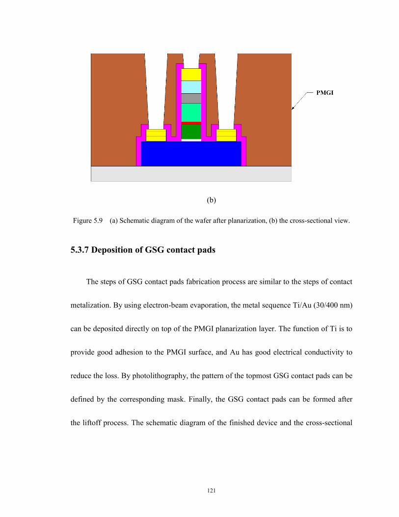
121
(b)
Figure 5.9 (a) Schematic diagram of the wafer after planarization, (b) the cross-sectional view.
5.3.7 Deposition of GSG contact pads
The steps of GSG contact pads fabrication process are similar to the steps of contact
metalization. By using electron-beam evaporation, the metal sequence Ti/Au (30/400 nm)
can be deposited directly on top of the PMGI planarization layer. The function of Ti is to
provide good adhesion to the PMGI surface, and Au has good electrical conductivity to
reduce the loss. By photolithography, the pattern of the topmost GSG contact pads can be
defined by the corresponding mask. Finally, the GSG contact pads can be formed after
the liftoff process. The schematic diagram of the finished device and the cross-sectional

122
view are illustrated in Fig. 5.10. Moreover, for the designed UTC-PD with 16 µm2 active
region, the suggested dimension parameters are stated in Fig. 5.11.
(a)
(b)
Figure 5.10 (a) Schematic diagram of finished device, (b) the cross-sectional view.
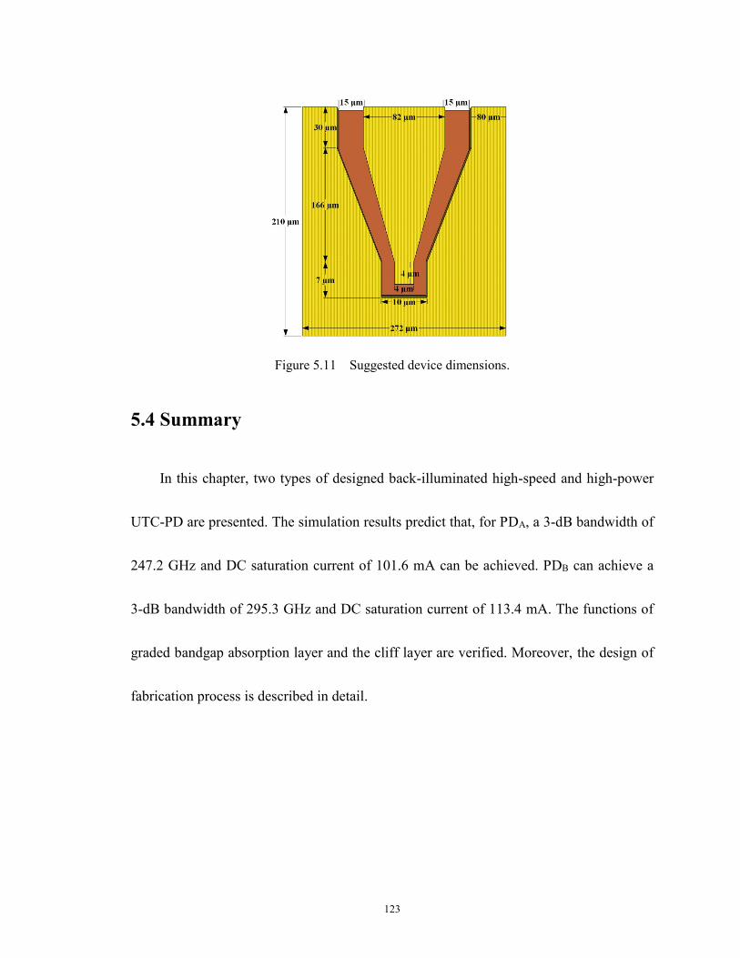
123
Figure 5.11 Suggested device dimensions.
5.4 Summary
In this chapter, two types of designed back-illuminated high-speed and high-power
UTC-PD are presented. The simulation results predict that, for PDA, a 3-dB bandwidth of
247.2 GHz and DC saturation current of 101.6 mA can be achieved. PDB can achieve a
3-dB bandwidth of 295.3 GHz and DC saturation current of 113.4 mA. The functions of
graded bandgap absorption layer and the cliff layer are verified. Moreover, the design of
fabrication process is described in detail.
124
Chapter 6 Conclusions and Future Work
6.1 Conclusions
The main focus of this work is to improve the bandwidth and saturation performance
of UTC-PD, since broadband and high-output-power PDs serve as the key component for
future high-frequency and high-power fiber-optic systems. First of all, it is verified that
the physics-based modeling of UTC-PDs can be used to predict the device performance,
as long as appropriate models and parameters are specified. The energy balance transport
model is employed, which includes the non-local effects such as velocity overshoot that
has been observed experimentally in UTC-PDs. The simulation results show good
agreement with the reported results. Consequently, the simulation results can be directly
used for device design.
The bandwidth of PD is determined by the carrier transit time τtr and RC-time
constant τRC. For UTC-PD, since the electron diffusion velocity in the absorption layer is
much slower than the electron drift velocity in the depletion region, the carrier transit
time τtr is mainly limited by the carrier traveling time τA in absorption layer. Therefore, in
order to improve the bandwidth performance, a built-in electric field can be constructed
in the absorption layer to accelerate the electrons. Using the physical modeling, it is

125
examined that, the 3-dB bandwidth can be enhanced by incorporating a linearly graded
doping profile in the absorption layer. Then, the graded bandgap absorption layer has
been further investigated. It is shown that a higher introduced built-in electric field in the
front part of absorption layer leads to a better bandwidth performance. By using the
optimized graded structure, the performance can be further improved. Moreover, the
effects of the proposed combined graded absorption layer structure is studied. It is
illustrated that, in the absorption layer, the combined introduced built-in electric field is
nearly the sum of the built-in electric fields constructed by graded doping structure and
graded bandgap structure. For PD80, the simulation result shows an improvement of
39.4% in bandwidth.
The space-charge effect is the dominant saturation mechanism at the bias voltage
considered in this work (-2V). Using the physical modeling, we analysed the
space-charge effect. It is shown that, at high light intensity, electrons are accumulated in
the absorption layer, and the electric field drops in the space layer, cliff layer, and also
the input end of collection layer, which lead to saturation. We also examined that, the
space-charge effect can be reduced by using the technique of charge compensation. The
investigation of charge compensation by using uniform doping in the collector indicates
that, higher collector doping level leads to better saturation performance. However, in
126
order to ensure the collection layer is completely depleted at normal device operation bias
voltage, the collector doping level cannot be too high. Then, we investigated the effects
of the proposed linearly doped collection layer, which can effectively compensate for the
space charge. It is shown that, the distribution of electric field is improved. The electric
field in the space layer, cliff layer and the collector input end is enhanced, which leads to
the better saturation performance. In addition, by comparing the distribution of electric
field of different linear doping cases, we found that, the saturation performance is not
only limited by the minimum electric field in the collection layer at high optical injection
level, but also is influenced by the electric field gradient. Accordingly, an optimized
Gaussian doping profile in the collection layer is proposed. For PD80, improvements of
18.7% and 25.8% in saturation current can be achieved by using optimized linear doping
profile and Gaussian doping profile respectively.
Additionally, the epitaxial layers of PDA and PDB were grown. For PDA, the
predicted bandwidth and saturation performance are 247.2 GHz and 101.6 mA,
respectively. For PDB, the predicted bandwidth and saturation performance are 295.3
GHz and 113.4 mA, respectively. The benefit of the proposed graded bandgap absorption
layer is further verified. The saturation current is enhanced due to the inserted cliff layer.
Moreover, the major fabrication process includes p-type contact metalization, p-mesa
127
formation, n-type contact metalization, n-mesa formation, passivation, planarization and
deposition of GSG contact pads.
6.2 Future work
Our future work is to complete the post process of the designed UTC-PDs. Then, the
measurements aim at various figures of merit, such as bandwidth, output power and
responsivity, will be carried out. Thereby, the effects of the proposed graded bandgap
absorption layer can be further verified. Moreover, the packaging techniques, such as
flip-chip bonding technology which can improve the thermal management capability, will
be investigated. Furthermore, the CPW-like interconnection structure will be investigated
and designed. Because, at such high operating frequency, the interconnection line may
cause great loss.
128
References
[1] A. Beling, “Periodic Travelling Wave Photodetectors with Serial and Parallel Optical
Feed Based on InP,” Ph. D. Dissertation, 2006.
[2] G.-F. D. Betta, “Advances in Photodiodes,” InTech, chap. 14, pp. 302, 2011.
[3] H. Yang, et al., “High-speed and high-power InGaAs/InP photodiode,” 23rd Intern.
Conf. On Indium Phosphide and Related Materials, Berlin, Germany, May 2011.
[4] K. Kato, S. Hata, K. Kawano, and A. Kozen, “Design of Ultrawide-Band,
High-Sensitivity p-i-n Photodetectors,” IEICE Trans. Electron., vol. E76-C, no. 2,
pp. 214-221, Feb. 1993.
[5] X. Li, et al., “High-saturation-current InP-InGaAs photodiode with partially depleted
absorber,” IEEE Photon. Technol. Lett., vol. 15, no. 9, pp. 1276-1278, Sep. 2003.
[6] T. Ishibashi, et al., “InP/InGaAs Uni-traveling-carrier Photodiodes,” IEICE Trans.
Electron, vol. E83-C, pp. 938-949, Jun. 2000.
[7] T. Ishibashi, S. Kodoma, N. Shimizu, and T. Furuta, “High-speed response of
uni-traveling-carrier photodiodes,” Jpn. J. Appl. Phys. 36, part 1, no. 10, pp.
6263-6268, 1997.
[8] T. Ishibashi, et al., “Uni-traveling-carrier photodiodes,” Ultrafast Electronics
129
Optoelectronics OSA Spring Topical Meeting, Technical Digest, pp. 166-168, 1997.
[9] H. Ito, et al., “High-speed and high-output InP-InGaAs unitraveling-carrier
photodiodes,” IEEE J. Sel. Top. Quantum Electron. 10(4), 709-727, 2004.
[10] B. Banik, J. Vukusic, H. Hjelmgren and J. Stake, “Optimization of the UTC-PD
Epitaxy for Photomixing at 340 GHz,” Int J Infrared Milli Waves, pp. 914-923, 2008.
[11] H. Ito, T. Furuta, S. Kodama, N. Watanabe, and T. Ishibashi, “InP/InGaAs
uni-travelling-carrier photodiode with 310 GHz bandwidth,” Electron. Lett., vol. 36,
no. 21, pp. 1809-1810, Oct. 2000.
[12] N. Shimizu, N. Watanabe, T. Furuta, and T. Ishib ashi, “InP-InGaAs
Uni-Traveling-Carrier Photodiode With Improved 3-dB Bandwidth of Over 150
GHz,” IEEE Photonics Technology Letters, vol. 10, no. 3, Mar. 1998.
[13] D.-H. Jun, J.-H. Jang, I. Adesida, and J.-I. Song, “Improved efficiency bandwidth
product of modified unitraveling carrier photodiode structures using an undoped
photo-absorption layer,” Jpn. J. Appl. Phys. 45(4B), pp. 3475-3478, 2006.
[14] X. Wang, N. Duan, H. Chen, and J. C. Campbell, “InGaAs-InP photodiodes with
high responsivity and high saturation power,” IEEE Photon. Technol. Lett. 19(16),
pp. 1272-1274, 2007.
[15] M. Chtioui, F. Lelarge, A. Enard, F. Pommereau, D. Carpentier, A. Marceaux, F.
130
van Dijk, and M. Achouche, “High responsivity and high power UTC and MUTC
GaInAs-InP photodiodes,” IEEE Photon. Technol. Lett. 24(4), pp. 318-320, 2012.
[16] Z. Li, H. Pan, H. Chen, A. Beling, and J. C. Campbell, “High-saturation-current
modified uni-traveling-carrier photodiode with cliff layer,” IEEE J. Quantum
Electron. 46(5), pp. 626-632, 2010.
[17] M. Chtioui, A. Enard, D. Carpentier, S. Bernard, B. Rousseau, F. Lelarge, F.
Pommereau, and M. Achouche, “High-performance uni-traveling-carrier photodiodes
with a new collector design,” IEEE Photon. Technol. Lett. 20(13), pp. 1163-1165,
2008.
[18] J.-W. Shi, Y.-S. Wu, C.-Y. Wu, P.-H. Chiu, and C.-C. Hong, “High-speed,
high-responsivity, and high-power performance of near-ballistic uni-traveling-carrier
photodiode at 1.55-µm wavelength,” IEEE Photon. Technol. Lett. 17(9), pp.
1929-1931, 2005.
[19] J.-W. Shi, F.-M. Kuo, and J. E. Bowers, “Design and analysis of ultra-high-speed
near-ballistic uni-travelingcarrier photodiodes under a 50-Ω load for high-power
performance,” IEEE Photon. Technol. Lett. 24(7), pp. 533-535, 2012.
[20] H. Fukano, Y. Muramoto, K. Takahata, and Y. Matsuoka, “High efficiency
edge-illuminated uni-travelling-carrier-structure refracting-facet photodiode,”
131
Electronics Letters 35(19), pp. 1664-1665, 1999.
[21] S. Demiguel, N. Li, X. Li, X. Zheng, J. Kim, J. C. Campbell, H. Lu, and A. Anselm,
“Very high-responsivity evanescently coupled photodiodes integrating a short planar
multimode waveguide for high-speed applications,” IEEE Photon. Technol. Lett.
15(12), pp. 1761-1763, 2003.
[22] J. Klamkin, S. M. Madison, D. C. Oakley, A. Napoleone, F. J. O’Donnell, M.
Sheehan, L. J. Missaggia, J. M. Caissie, J. J. Plant, and P. W. Juodawlkis,
“Uni-traveling-carrier variable confinement waveguide photodiodes,” Opt. Express
19(11), pp. 10199-10205, 2011.
[23] M. Hosseinifar, V. Ahmadi, and G. Abaeiani, “Microring-based unitraveling carrier
photodiodes for high bandwidth-efficiency product photodetection in optical
communication,” J. Lightwave Technol. 29(9), pp. 1285-1292, 2011.
[24] Y. Muramoto, K. Kato, M. Mitsuhara, O. Nakajima, Y. Matsuoka, N. Shimizu and
T. Ishibashi, “High-output-voltage, high speed, high efficiency uni-travelling-carrier
waveguide photodiode,” Electronics Letters, vol. 34, no. 1, 8th Jan. 1998.
[25] N. Duan, X. Wang, N. Li, H. D. Liu, and J. C. Campbell, “Thermal analysis of
high-power InGaAs-InP photodiodes,” IEEE J. Quantum Electron., vol. 42, no. 12,
pp. 1255-1258, Dec. 2006.
132
[26] Z. Li, et al., “High-power high-linearity flip-chip bonded modified uni-traveling
carrier photodiode,” Opt. Express, vol. 19, no. 26, pp. B385-B390, 2011.
[27] Q. Zhou, A. Cross, Y. Fu, A. Beling, and J. C. Campbell, “High-power
high-bandwidth flip-chip bonded modified uni-traveling carrier photodiodes,” Proc.
IEEE Photon. Conf., pp. 306-307, Sep. 2012.
[28] J.-W. Shi, F.-M. Kuo, C.-J. Wu, C. L. Chang, C.-Y. Liu, C. Y. Chen, and J.-I. Chyi,
“Extremely high saturation current-bandwidth product performance of a
near-ballistic uni-traveling-carrier photodiode with a flip-chip bonding structure,”
IEEE J. Quantum Electron. 46(1), pp. 80-86, 2010.
[29] H. Ito, T. Furuta, S. Kodama, N. Watanabe, and T. Ishibashi, “InP/InGaAs
uni-travelling-carrier photodiode with 220 GHz bandwidth,” Electron. Lett., vol. 35,
pp. 1556-1557, Sep. 1999.
[30] “ATLAS User’s Manual,” SILVACO Inc., Santa Clara, Mar. 2012.
[31] S. M. Mahmudur Rahman, H. Hjelmgren, J. Vukusic, J. Stake, P. A. Andrekson,
and H. Zirath, “Hydrodynamic simulations of unitraveling-carrier photodiodes,”
IEEE J. Quantum Electron., vol. 43, no. 11, pp. 1088-1094, Nov. 2007.
[32] http://www.ioffe.rssi.ru/SVA/NSM/.
[33] S. Adachi, “Physical Properties of III-V Semiconductor Compounds: InP, InAs,
133
GaAs, GaP, InGaAs and InGaAsP, Wiley Interscience,” John Wiley and Sons, 1992.
[34] S. Srivastava, “Simulation study of InP-based uni-traveling carrier photodiode,”
Master Thesis, University of Cincinnati, 2003.
[35] http://en.wikipedia.org/wiki/Refractive_index.
[36] S. Adachi, “Optical Constants of Crystalline and Amorphous Semiconductors,”
Kluwer Academic Publishers, Boston, pp. 359-362, 1999.
[37] M. Levinshtein, S. Rumyantsev, M. Shur, “Handbook Series on Semiconductor
Parameters,” World Scientific, New Jersey, Chap. 7, pp. 156, 1999.
[38] R. Stratton, “Diffusion of hot and cold electrons in semiconductor barriers,” Phys.
Rev. 126(6), pp. 2002-2014, 1962.
[39] R. Stratton, “Semiconductor current-flow equations (diffusion and degeneracy),”
IEEE Trans. Electron. Dev. 19(12), pp. 1288-1292, 1972.
[40] M. Shur, “Physics of Semiconductor Devices,” Prentice Hall, New Jersey, pp. 74,
1990.
[41] Caughey, D.M., and R.E. Thomas, “Carrier Mobilities in Silicon Empirically
Related to Doping and Field,” Proc. IEEE 55, pp. 2192-2193, 1967.
[42] M. M Tashima, L.W Cook, and G.E Stillman, “Room temperature electron diffusion
lengths in liquid phase epitaxial InGaAsP and InGaAs,” Appl. Phys. Letters, vol. 39,
134
pp. 960-961, 1981.
[43] T. Conklin, S. Naugle, S. Shi, K.P. Roenker, S.M Frimel, T. Kumar, M.M Cahay,
“Inclusion of tunneling and ballistic transport effects in an analytical approach to
modeling of NPN InP based heterojunction bipolar transistors ,” Superlatt.
Microstruct., vol. 18, pp. 1-12, 1996.
[44] Dziewior J. and W. Schmid, “Auger Coefficient for Highly Doped and Highly
Excited Silicon,” Appl. Phys. Lett. vol. 31, pp. 346-348, 1977.
[45] R. Zhang, B. Hraimel, X. Li, P. Zhang, and X.-P. Zhang, “Design of broadband and
high-output power uni-traveling-carrier photodiodes,” Optics Express, vol. 21, no. 6,
2013.
[46] T. P. Pearsall, “GaInAsP Alloy Semiconductors,” John Wiley and Sons, 1982.
[47] S. O. Kasap, “Optoelectronics and Photonics: Principles and Practices,” Prentice
Hall, pp. 222, 2001.
[48] P. Liu, K. J. Willaims, M. Y. Frankel, and R. D. Esman, “Saturation Characteristics
of Fast Photodetectors,” IEEE Trans. on Microwave Theory and Tech., vol. 47, no. 7,
pp. 1297-1303, 1999.
[49] K. J. Williams and R. D. Esman, “Design considerations for high-current
photodetectors,” J. Lightwave Technol., vol. 17, pp. 1443-1454, Aug. 1999.
135
[50] W. Fawcett and G. Hill, “Temperature dependence of the velocity/field
characteristic of electrons in InP,” Electron. Lett., vol. 11, no. 4, pp. 80-81, Feb.
1975.
[51] N. Li, X. Li, S. Demiguel, X. Zheng, J. Campbell, D. Tulchinsky, J. Williams, T.
Isshiki , G. Kinsey, and R. Sudharsansan, “High-saturat ion-current
charge-compensated InGaAs-InP UTC photodiode,” IEEE Photon. Technol. Lett.,
vol. 16, no. 3, pp. 864-866, Mar. 2004.
[52] D. A. Anderson, N. Aspley, P. Davies, and P. L. Giles, “Compensation in heavily
doped n-type InP and GaAs,” J. Appl. Phys., vol. 58, no. 8, pp. 3060-3067, 1985.
[53] T. J. Maloney and J. Frey, “Transient and steady-state electron transport properties
of GaAs and InP,” J. Appl. Phys., vol. 48, no. 2, pp. 781-787, 1977.
[54] M. Chtioui, et al., “High Power UTC Photodiodes Design and Application for
Analog Fiber Optic Links,” Proc. IEEE Int. Topical Meeting Microwave Photonics,
pp. 1-4, 2009.
[55] R. C. Jaeger, “Introduction to Microelectronic Fabrication,” 2nd edition, Prentice
Hall, pp. 156, 2002.
[56] D. A. Neamen, “Semiconductor Physics and Devices: Basic Principles,” 3rd edition,
McGrdw-Hill, pp. 348, 2003.