Embed Size (px)
Citation preview
INTL JOURNAL OF ELECTRONICS AND TELECOMMUNICATIONS, 2019, VOL. 65, NO. 4, PP. 619-624
Manuscript received July 8, 2019; revised September, 2019. DOI: 10.24425/ijet.2019.129821
Abstract—The paper presents a concept of a control system for
a high-frequency three-phase PWM grid-tied converter
(3x400 V / 50 Hz) that performs functions of a 10-kW DC power
supply with voltage range of 600÷800 V and of a reactive power
compensator. Simulation tests (in PLECS) allowed proper
selection of semiconductor switches between fast IGBTs and
silicon carbide MOSFETs. As the main criterion minimum
amount of power losses in semiconductor devices was adopted.
Switching frequency of at least 40 kHz was used with the aim of
minimizing size of passive filters (chokes, capacitors) both on the
AC side and on the DC side. Simulation results have been
confirmed in experimental studies of the PWM converter, the
power factor of which (inductive and capacitive) could be
regulated in range from 0.7 to 1.0 with THDi of line currents
below 5% and energy efficiency of approximately 98.5%. The
control system was implemented in Texas Instruments
TMS320F28377S microcontroller.
Keywords—Three-phase PWM rectifier, reactive power
compensator, silicon carbide MOSFET, bidirectional power flow,
direct power control (DPC), DC voltage regulation, power factor
correction (PFC), LCL filter
I. INTRODUCTION
HE newest power transistors like IGBTs or silicon
carbide MOSFETs can be used in high-switching-
frequency and high-power converters. Over the last few years
the wide band gap (WBG) devices have been becoming
increasingly important, because their blocking voltage values
of over 1 kV allow them to be used in three-phase grid-tied
converters at 3x400 V and 50 Hz [1][2][3][4]. Due to high
achievable switching frequency and low power losses in SiC
MOSFETs, useful properties of the converter are also
obtained, such as high power density, small grid filter
dimensions, high energy efficiency and small distortions of the
grid currents [5][6].
This creates unprecedented possibilities of using power
converters in the power system on a large scale. Particularly
important applications of WBG converters are: renewable
energy sources (RES) [7][8], improvement of power system
quality parameters (active filters) [9][10], integration of
consumers and energy sources with different parameters in
smart grids (solid state transformers - SST [11][12]) and EV
chargers [13][14].
This paper was supported by the statute funds of Institute of Control and
Industrial Electronics, Warsaw University of Technology. The authors are with Warsaw University of Technology, Warsaw, Poland
(e-mail: [email protected], [email protected],
The paper presents selected design problems and
experimental investigations of a bidirectional three-phase grid-
tied converter with a power level of 10 kW and a 600÷800 V
DC voltage range. The main task of the converter is to supply
DC power with a unity power factor; however, the system can
also be used as a reactive power compensator with adjustable
power factor and as a coupling link between the power system
and energy storage system in voltage range from 600 to 800 V.
Selection of the main components like power transistors or
AC and DC filter, as well as control system with direct power
factor correction, were evaluated through simulation studies.
The main condition for the selection of power switches from
the available IGBTs and silicon carbide MOSFETs was to
minimize switching and conduction power losses with the
assumption of the switching frequency of at least 40 kHz.
Simulation results and analytical calculations were verified
in experimental studies, where the prototype of the converter
with SiC transistors was tested. The developed control system
allows to set the DC voltage value as well as to directly adjust
power factor value in the range from 0.7 to 1.0. In
experimental measurements of switching power losses,
oscilloscope observations and measurements with power
analyzer were used [15]. System has also been tested in the
inverter mode, i.e. when transferring energy from the DC side
to the AC side.
II. ANALYTICAL AND SIMULATION STUDIES
Table I presents the most important design assumptions for
the bidirectional three-phase PWM converter. The electrical
scheme of the system, developed for the simulation in the
PLECS environment, is shown in Fig. 1. A two-level PWM
converter is characterized by a simple construction and a small
number of semiconductor devices, but it requires the use of
larger passive components to obtain currents and voltages with
lower values of total harmonic distortion compared to multi-
level topologies.
Investigation of a High-efficiency and High-
frequency 10-kW/800-V Three-phase PWM
Converter with Direct Power Factor Control Roman Barlik, Piotr Grzejszczak, Bernard Leszczyński, and Marek Szymczak
T
TABLE I
DESIGN PARAMETERS
Parameter Symbol Value
Phase voltage of the grid Vac 3x230 V
Maximum DC voltage Vdc 800 V
Nominal apparent power S 10 kVA Range of power factor change λ 0.7 ÷ 1.0
Relative ripple of DC voltage ΔVdc% 5%
Total harmonic distortion of current THDi 5% RMS value of rated current Irms 15 A
Minimum switching frequency fsw 40 kHz
TABLE I
[TABLE TITLE] TABLE NAME
Column 1 Column 2 Column 3 a
xx1 yyy1 zzz1
xxx2 yy2 zzz2
620 R. BARLIK, P. GRZEJSZCZAK, B. LESZCZYŃSKI, M. SZYMCZAK
Fig. 1. Circuit model of the PWM converter with MOSFET switches
A. Control System
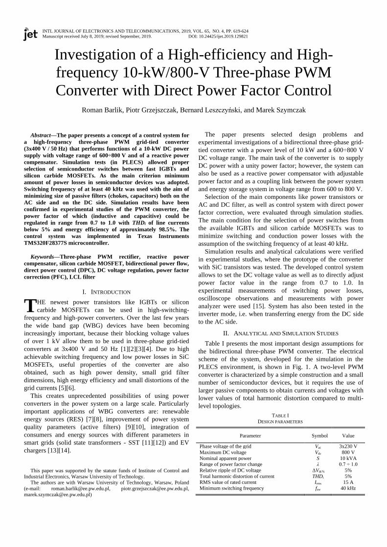
In the first stage of simulation tests, the correctness of the control system operation was verified. The main task of the control algorithm is stabilization of output voltage Vdc around a reference value while controlling the value of power factor λ at the same time. Moreover, sinusoidal modulation of voltage pulses on the AC side of the converter is provided.
Fig. 2. Control system with direct power factor regulation: block diagram (a)
and its implementation in a simulation model (b)
The control algorithm uses the transformation of measurement signals from three-phase system to the rotating reference system d-q, which allows the use of simple PI regulators (Fig. 2) [16]. The transformation of three-phase voltages and currents to the d–q system is provided by the blocks abc -> dq. In each such block, in addition to signals proportional to the instantaneous values of phase currents or voltages, a value of the angle φ between current and voltage waveforms, obtained from phase-locked loop (PLL), is applied
[17]. After determining the RMS values of voltage (Vrms) and
current (Irms) and average value of apparent (S) and active (P) power, the power factor λ = P / S is calculated, which, assuming only a slight distortion of the grid current (THDi < 5%), is approximately equal to the value of cosϕ. In the adopted control algorithm the power factor is influenced by changes in the passive component of the grid current vector - Iq. The setpoint value of this component determines the value of the power factor. On the other hand, the Vdc voltage regulator acts on the active component Id of the grid current vector, which is proportional to the active power P taken from the grid.
To check the operation of the power factor control algorithm, a simulation was performed, in which the reference value of the power factor was changed from 1.0 to 0.8 (at constant active power value P = 6 kW). The proposed algorithm was written using C-script block to most accurately reflect the operation of a real digital controller. Results of this study, presented in Fig. 3, confirm the theoretical analysis and correct operation of the control algorithm.
Fig. 3. Results of the operation of the converter during step change of the
power factor (a-c) and step change of the load resistance (d) – simulation
studies
INVESTIGATION OF A HIGH-EFFICIENCY AND HIGH-FREQUENCY 10-KW/800-V THREE-PHASE PWM CONVERTER… 621
B. Design of AC and DC filters
The study of a simplified converter simulation model with
ideal semiconductor switches also showed correct operation of
the space vector modulator (SVM). The control algorithm
provides a sinusoidal shape of waveforms of the AC grid
currents, which depends not only on the modulation method,
but also on the switching frequency (fs = 40 kHz) and the type
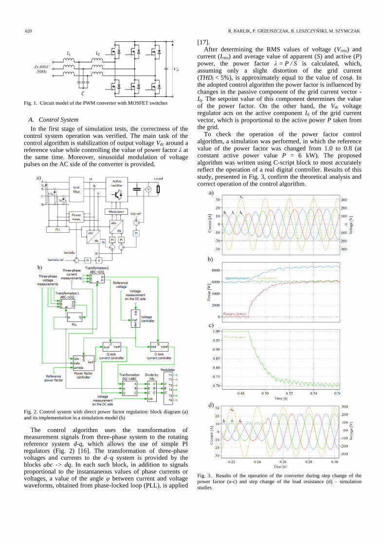
of the grid filter (Fig. 4). In order to select the filter
parameters, grid current THDi minimization (less than 5%) as
well as minimization of geometrical dimensions, power losses
and costs were all taken into account. Literature analysis [18]
and simulation study have shown that these criteria are best
met by the filter according to Fig. 4c with 1.8 mH < L1 < 6
mH; C = 1.5 μF; L2 = 150 μH, meeting the condition of 10f <
frez < 0.5fsw, where f = 50 Hz and
𝑓𝑟𝑒𝑧 =1
2𝜋√𝐿1+𝐿2
𝐿1𝐿2𝐶 (1)
Fig. 4. Alternate filter versions on the AC line side: (a) L filter; (b) LC filter;
c) LCL filter
When selecting DC filter capacitors, it was assumed that the
peak-to-peak ripple value of the output voltage ΔVdc% should
be below 5% of the average value of this voltage. Simulation
tests have shown that in addition to the DC filter capacitance,
switching frequency and the load current, the distortion and
asymmetry of the supply grid currents have influence on the
value of ΔVdc%. A slight dependence between ripple ΔVdc% and
the deadtime between PWM signals was also observed.
Multilateral simulation tests for the nominal conditions
allowed to determine the final value of DC capacitance as
CDC = 1 mF.
C. Semiconductor Components
When choosing diodes and transistors, typical criteria were
adopted, including: maximum blocking voltages (1200 V),
permissible current carrying capacity (ITrms > 15 A),
minimization of conduction (diodes: PC-D, transistors: PC-
MOSFET and PC-IGBT) and switching (diodes: PSW-D, transistors:
PSW-MOSFET; PSW-IGBT) power losses. Initial analysis of available
semiconductor devices allowed to select switches (transistors
with free-wheeling diodes) with the following designations:
SK35GD126ET and SKiiP25AC12F4V19 (IGBT);
SCT3080KL, C2M0040120D and LSIC1M0120E0080
(MOSFET SiC). In order to determine the power losses
dissipated in the semiconductor switches, a simulation model
of the converter was built and tested, and the obtained results
were used to calculate power losses based on the following
formulas:
𝑃𝐶 _ 𝐼𝐺𝐵𝑇 = 𝑉𝐶𝐸0𝐼𝐴𝑉 _ 𝑇 + 𝑟𝑇𝐼𝑅𝑀𝑆 _𝑇2 (2)
𝑃𝐶 _𝑀𝑂𝑆𝐹𝐸𝑇 = 𝑟𝑇𝐼𝑅𝑀𝑆 _𝑇2 (3)
𝑃𝐶 _ 𝐷 = 𝑉𝐹0𝐼𝐴𝑉 _𝐷 + 𝑟𝐷𝐼𝑅𝑀𝑆 _ 𝐷2 (4)
𝑃𝑆𝑊 _ 𝐼𝐺𝐵𝑇 = 𝑓𝑆𝑊(𝐸𝑂𝑁 + 𝐸𝑂𝐹𝐹)𝐼𝐴𝑉 _𝑇/𝐼𝑅𝑀𝑆 _𝑇 (5)
𝑃𝑆𝑊 _𝑀𝑂𝑆𝐹𝐸𝑇 = 𝑓𝑆𝑊𝑉𝑑𝑐𝐼𝑅𝑀𝑆 _ 𝑇(𝑡𝑂𝑁 + 𝑡𝑂𝐹𝐹) (6)
𝑃𝑆𝑊 _𝐷 = 𝑓𝑆𝑊𝐸𝑟𝑒𝑐𝐼𝐴𝑉 _𝐷/𝐼𝑅𝑀𝑆 _𝐷 (7)
where: VCE0, VF0 - threshold voltage values of the IGBT
transistor and the diode; IAV-T, IAV-D - average values of
transistor and diode currents; IRMS-T, IRMS-D - effective values of
transistor and diode currents; EON, EOFF - energy loss caused by
switching the component on and off; Erec - loss of energy when
switching off the diode; rT, rD - transistor and diode resistance
in the conduction state.
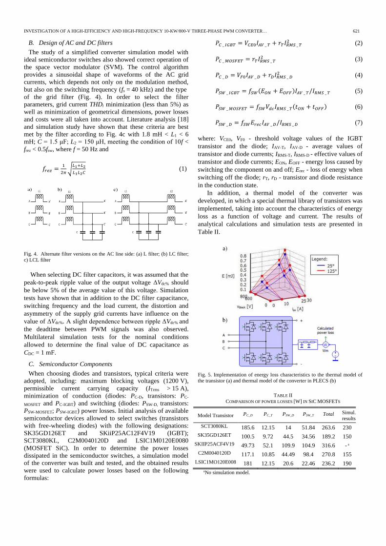
In addition, a thermal model of the converter was
developed, in which a special thermal library of transistors was
implemented, taking into account the characteristics of energy
loss as a function of voltage and current. The results of
analytical calculations and simulation tests are presented in
Table II.
Fig. 5. Implementation of energy loss characteristics to the thermal model of
the transistor (a) and thermal model of the converter in PLECS (b)
TABLE II
COMPARISON OF POWER LOSSES [W] IN SIC MOSFETS
Model Transistor PC_D PC_T PSW_D PSW_T Total Simul.
results
SCT3080KL 185.6 12.15 14 51.84 263.6 230
SK35GD126ET 100.5 9.72 44.5 34.56 189.2 150
SKIIP25ACF4V19 49.73 52.1 109.9 104.9 316.6 - a
C2M0040120D 117.1 10.85 44.49 98.4 270.8 155
LSIC1MO120E008 181 12.15 20.6 22.46 236.2 190
aNo simulation model.
TABLE I
[TABLE TITLE] TABLE NAME
Column 1 Column 2 Column 3 a
xx1 yyy1 zzz1
xxx2 yy2 zzz2
xxx3 yyy3 zz3 xxx4 yy4 zzzzz4
xxx5 yyyyy5 zz5
622 R. BARLIK, P. GRZEJSZCZAK, B. LESZCZYŃSKI, M. SZYMCZAK
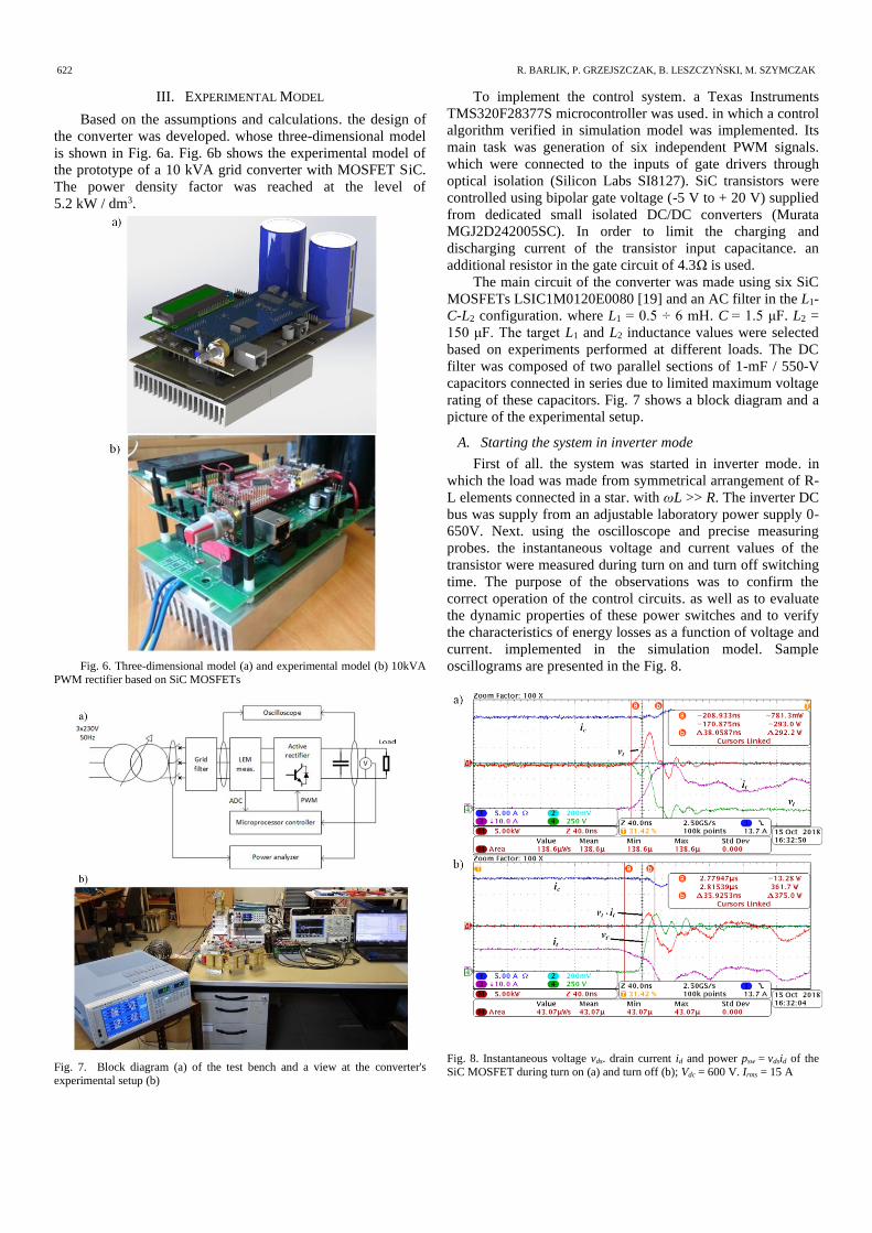
III. EXPERIMENTAL MODEL
Based on the assumptions and calculations. the design of
the converter was developed. whose three-dimensional model
is shown in Fig. 6a. Fig. 6b shows the experimental model of
the prototype of a 10 kVA grid converter with MOSFET SiC.
The power density factor was reached at the level of
5.2 kW / dm3.
Fig. 6. Three-dimensional model (a) and experimental model (b) 10kVA
PWM rectifier based on SiC MOSFETs
Fig. 7. Block diagram (a) of the test bench and a view at the converter's
experimental setup (b)
To implement the control system. a Texas Instruments
TMS320F28377S microcontroller was used. in which a control
algorithm verified in simulation model was implemented. Its
main task was generation of six independent PWM signals.
which were connected to the inputs of gate drivers through
optical isolation (Silicon Labs SI8127). SiC transistors were
controlled using bipolar gate voltage (-5 V to + 20 V) supplied
from dedicated small isolated DC/DC converters (Murata
MGJ2D242005SC). In order to limit the charging and
discharging current of the transistor input capacitance. an
additional resistor in the gate circuit of 4.3Ω is used.
The main circuit of the converter was made using six SiC
MOSFETs LSIC1M0120E0080 [19] and an AC filter in the L1-
C-L2 configuration. where L1 = 0.5 ÷ 6 mH. C = 1.5 μF. L2 =
150 μF. The target L1 and L2 inductance values were selected
based on experiments performed at different loads. The DC
filter was composed of two parallel sections of 1-mF / 550-V
capacitors connected in series due to limited maximum voltage
rating of these capacitors. Fig. 7 shows a block diagram and a
picture of the experimental setup.
A. Starting the system in inverter mode
First of all. the system was started in inverter mode. in
which the load was made from symmetrical arrangement of R-
L elements connected in a star. with ωL >> R. The inverter DC
bus was supply from an adjustable laboratory power supply 0-
650V. Next. using the oscilloscope and precise measuring
probes. the instantaneous voltage and current values of the
transistor were measured during turn on and turn off switching
time. The purpose of the observations was to confirm the
correct operation of the control circuits. as well as to evaluate
the dynamic properties of these power switches and to verify
the characteristics of energy losses as a function of voltage and
current. implemented in the simulation model. Sample
oscillograms are presented in the Fig. 8.
Fig. 8. Instantaneous voltage vds. drain current id and power psw = vdsid of the
SiC MOSFET during turn on (a) and turn off (b); Vdc = 600 V. Irms = 15 A
INVESTIGATION OF A HIGH-EFFICIENCY AND HIGH-FREQUENCY 10-KW/800-V THREE-PHASE PWM CONVERTER… 623
Fig. 9. Switching energy vs drain current characteristic for
LSIC1M0120E0080 MOSFET [18]. (red – measured energy for Vdc = 600V)
As can be seen in Fig. 8 and Fig. 9. the recorded values of
the switching on and off energy of the SiC transistor coincide
with values declared in the manufacturer datasheet [19]. This
also confirms the correctness of the data for the thermal model
of the SiC transistor in simulation tests.
B. Converter power losses - experimental measurements
The power losses of PWM rectifier were determined as the
difference between the active power obtained from the grid
and the power measured at the DC side. To estimate power
losses of the converter. input and output power values were
measured for different switching frequencies. Based on these
measurements. conduction and switching power losses was
calculated. Assuming that the conduction losses in the
converter (Pc = 55W) are independent of the switching
frequency. the converter losses can be separated from losses in
the grid filter.
Fig. 10. Power losses in PWM rectifier with LCL filter for different switching
frequencies at 6kW
Results of the experimental measurements of the converter
power losses for P = 6 kW for different switching frequencies.
were presented in Table III and Fig. 10.
The obtained results indicate that with use of L1 = 6 mH.
THDi is less than 2% and the energy efficiency of the converter
at P = 6 kW and fsw = 40 kHz is around 98.5% (Fig. 11)
Fig. 11. Experimental and theoretical results of total power losses in the PWM
rectifier at active power value P = 6 kW. fsw = 40 kHz
C. Power quality and control system dynamics tests
The measurements of THDi coefficient for different grid filter
configurations were conducted using Yokogawa WT1800
power analyzer (Fig. 12). Three LCL filter configurations were
used for the tests. in which the value of L1 inductors (0.5 mH.
1.8 mH and 6 mH) was changed. The results of the THDi
measurements of the grid current are shown in Fig. 11. It
shows that even with 1.8 mH inductance the requirements of
standards regarding the content of higher harmonics are met
(below 5%).
Fig. 12. THDi factor of the line current for different values of inductance L1 of
the AC filter L1-C-L2
Experimental tests were also carried out to determine the
compensating properties of the converter (Fig. 13) and
dynamics of the control system (Fig. 14). Presented waveforms
confirm correct operation of the converter and control system.
which implements all design assumptions.
IV. CONCLUSIONS
A full research cycle is presented. the result of which is the
design. construction and testing of an experimental three-phase
model (3x400 V / 50 Hz) of a 10-kW PWM converter built
with silicon carbide MOSFETs. selected from the ever richer
offer of these elements. The use of PLECS simulation program
and the C-language algorithm significantly improves the
implementation of the control system realized using a fast DSP
microcontroller. Thanks to the use of fast SiC transistors
switched at 40 kHz. it was possible to obtain instantaneous
grid currents with very low harmonic distortion values (THDi
< 2%) at small dimensions of the grid filter. According to the
TABLE III
RESULTS OF THE EXPERIMENTAL POWER LOSSES MEASUREMENTS
Switching frequency [kHz] 20 40 60 80
Total power losses [W] 113.8 127.9 146.3 163.7
Power losses in the converter [W] 73 91 109 127
Power losses in grid filter [W] 40.8 36.9 37.3 36.7
TABLE I
[TABLE TITLE] TABLE NAME
Column 1 Column 2 Column 3 a
xx1 yyy1 zzz1
xxx2 yy2 zzz2
xxx3 yyy3 zz3 xxx4 yy4 zzzzz4
xxx5 yyyyy5 zz5
a[Footnote Text] Content.

624 R. BARLIK, P. GRZEJSZCZAK, B. LESZCZYŃSKI, M. SZYMCZAK
assumptions. in the load range of up to 10 kVA the converter
can fulfill not only the function of a power supply (with bi-
directional energy flow). but also that of a reactive power
compensator. The results of measurements of power losses
dissipated in the whole system show a far-reaching
convergence with the analytical results and simulation
calculations and confirm the high energy efficiency of the
tested system (98.5%). Great practical advantages of the
PLECS program. which offers the possibility of creating
thermal profiles of semiconductor devices and easy selection
of heat sinks. have been confirmed.
Fig. 13. Grid voltage and current waveforms at unity power factor (a) and
phase shift between voltage va and grid current ia for λ = 0.7 (b)
Fig. 14. DC voltage vdc and grid current waveforms at step changes of
reference DC voltage value (a) and reference power value (b)
REFERENCES
[1] J. C. Balda and A. Mantooth. "Power-Semiconductor Devices and Components for New Power Converter Developments: A key enabler for
ultrahigh efficiency power electronics." in IEEE Power Electronics
Magazine. vol. 3. no. 2. pp. 53-56. June 2016. [2] F. F. Wang and Z. Zhang. "Overview of silicon carbide technology:
Device. converter. system. and application." in CPSS Transactions on
Power Electronics and Applications. vol. 1. no. 1. pp. 13-32. Dec. 2016. [3] S. Piasecki and J. Rąbkowski. "The 10 kVA SiC-based grid connected
AC/DC converter with extended functionalities — Experimental
investigation." 2016 10th International Conference on Compatibility. Power Electronics and Power Engineering (CPE-POWERENG).
Bydgoszcz. 2016. pp. 214-218.
[4] F. Xu. B. Guo. L. M. Tolbert. at all. "Evaluation of SiC MOSFETs for a high efficiency three-phase buck rectifier." 27th Annual IEEE Appl.
Power Electr.Conf. and Exp. (APEC). Orlando. FL. 2012. pp. 1762-
1769. [5] A. Kouchaki and M. Nymand. "Efficiency Evaluation of Three-phase
SiC Power Factor Correction Rectifier with Different Controllers." 2018
20th European Conference on Power Electronics and Applications (EPE'18 ECCE Europe). Riga. 2018. pp. P.1-P.10.
[6] A. Stupar. T. Friedli. J. Minibock at all. "Towards a 99% Efficient Three-
Phase Buck-Type PFC Rectifier for 400-V DC Distribution Systems." in IEEE Trans. on Power Electr.. vol. 27. no. 4. pp. 1732-1744. 2012.
[7] S. Wall. X. Hong. L. Sha and J. Xie. "High-efficiency PV inverter with
SiC technology." in IET Renewable Power Generation. vol. 12. no. 2. pp. 149-156. 2018.
[8] B. Zhao. Q. Yu. and W. Sun. “Wide-band gap devices in PV systems
opportunities and challenges.” IEEE Transactions on Power Electronics. vol. 27. no. 11. pp. 4667–4680. Nov 2012
[9] S. Hamasaki. K. Nakahara and M. Tuji. "Harmonics Compensation in
High Frequency Range of Active Power Filter with SiC-MOSFET Inverter in Digital Control System." 2018 International Power
Electronics Conference. Niigata. 2018. pp. 3237-3242.
[10] D. Kranzer. J. Thoma. B. Volzer. D. Derix and A. Hensel. "Development
of a 10 kV three-phase transformerless inverter with 15 kV Silicon
Carbide MOSFETs for grid stabilization and active filtering of harmonics." 2017 19th European Conference on Power Electronics and
Applications (EPE'17 ECCE Europe). Warsaw. 2017. pp. P.1-P.8.
[11] S. Madhusoodhanan et al.. "Solid-State Transformer and MV Grid Tie Applications Enabled by 15 kV SiC IGBTs and 10 kV SiC MOSFETs
Based Multilevel Converters." in IEEE Transactions on Industry
Applications. vol. 51. no. 4. pp. 3343-3360. July-Aug. 2015. [12] J. E. Huber. J. Böhler. D. Rothmund and J. W. Kolar. "Analysis and cell-
level experimental verification of a 25 kW all-SiC isolated front end 6.6
kV/400 V AC-DC solid-state transformer." in CPSS Transactions on Power Electronics and Applications. vol. 2. no. 2. pp. 140-148. 2017.
[13] A. Khaligh and M. D'Antonio. "Global Trends in High-Power OnBoard
Chargers for Electric Vehicles." in IEEE Transactions on Vehicular Technology. vol. 68. no. 4. pp. 3306-3324. April 2019.
[14] C. Jiang. B. Lei. H. Teng and H. K. Bai. "The power-loss analysis and
efficiency maximization of a silicon-carbide MOSFET based three-phase 10kW bi-directional EV charger using variable-DC-bus control." 2016
IEEE Energy Conversion Congress and Exposition (ECCE). Milwaukee.
WI. 2016. pp. 1-6. [15] Grzejszczak P.. „ Methodology for determining power losses in
switching devices of dual active bridge converter with taking into
account the thermal effects”. PhD thesis. Warsaw University of Technology. 2014.
[16] M. Malinowski. M. Jasinski and M. P. Kazmierkowski. "Simple direct
power control of three-phase PWM rectifier using space-vector modulation (DPC-SVM)." in IEEE Transactions on Industrial
Electronics. vol. 51. no. 2. pp. 447-454. April 2004.
[17] W. Phips W.. M. J. Harrison and R. M. Duke. „Three-Phase Phase-Locked Loop Control of a New Generation Power Converter.” 2006 1ST
IEEE Conf. on Ind.Electr. and Appl.. Singapore. 2006. pp.1-6.
[18] C. Nardi. C. M. Stein. E. G. Carati. at all..”A methodology of LCL filter design for grid-tied Power converters”. IEEE 13th Brazilian Power
Electron. and 1st Southern Power Electron. Conf.. Fortaleza. 2015.
[19] Datasheet MOSFET SiC LSIC1M0120E0080. online: https://www.littelfuse.com (2019)