Embed Size (px)
Citation preview
Investigation of a Phased Array of Circular
Microstrip Patch Elements Conformal to a
Paraboloidal Surface
Sharath Kumar
Thesis submitted to the faculty of the
Virginia Polytechnic Institute and State University
in partial fulfillment of the requirements for the degree
Master of Science
In
Electrical Engineering
Dr Amir I Zaghloul Chair
Dr William A Davis
Dr Lamine M Mili
September 11th
2006
Falls Church Virginia
Keywords Paraboloidal Arrays Conformal Arrays
Circular Microstrip Patch Arrays
Copyright 2006 Sharath Kumar
ii
Investigation of a Phased Array of Circular Microstrip Patch Elements
Conformal to a Paraboloidal Surface
Sharath Kumar
Abstract
This thesis investigates the performance of a phased array of antenna elements conforming to a
paraboloidal surface We hypothesize that such a conformal phased array would have
performance comparable to that of a correspondingly sized planar array The performance of a
paraboloidal array of antenna elements was simulated using an array program and the resulting
gains side-lobe levels and half-power beamwidths compared to those of a similarly sized planar
array Furthermore we propose a beam-forming feed network for this paraboloidal phased array
and discuss the influence that coupling between the elements could have on the array
performance Lastly we propose that such an array be used in conjunction with a parabolic
reflector antenna to form a versatile hybrid antenna with several potential applications
iii
Acknowledgments
I would like to take this opportunity to earnestly thank Dr Amir I
Zaghloul my advisor for his patient guidance and support in making this work
possible I also wish to acknowledge the help of Maryam Parsa who contributed to
various aspects of this work Lastly I would like to thank the faculty of Virginia
Tech for making the experience of graduate school enriching and fulfilling
iv
Contents
Abstract ii
Acknowledgments iii
List of Figures and Tables helliphelliphelliphelliphelliphelliphelliphelliphelliphelliphelliphelliphelliphelliphelliphelliphelliphelliphelliphelliphelliphelliphelliphelliphellipv
Chapter 1 Introduction 1
11 Motivation and Background 1
12 Objective 1
13 Brief Description of Arrayhelliphelliphelliphelliphelliphelliphelliphelliphelliphelliphelliphelliphelliphelliphelliphelliphelliphelliphelliphellip2
14 Organization of Thesishelliphelliphelliphelliphelliphelliphelliphelliphelliphelliphelliphelliphelliphelliphelliphelliphelliphelliphelliphelliphellip2
Chapter 2 Background Microstrip Antenna Arrays 4
21 Array Theory 4
22 Circular Microstrip Patch Antennashelliphelliphelliphelliphelliphelliphelliphelliphelliphelliphelliphelliphelliphelliphelliphellip6
23 Microstrip Arrays 9
Chapter 3 The Paraboloidal Array Parameters and Configuration 10
Chapter 4 Paraboloidal Array Performance General Discussion 14
41 Assessment of Array Performance 14
42 Scanning and Phase Quantization Background and Performance 18
Chapter 5 Simulation Results and Analysis 21
51 Scanning Simulation Results and Analysis 21
52 Phase-Quantized Scanning Simulation Results and Analysis 34
53 Summary of Simulation Results 50
Chapter 6 Discussion on Mutual Coupling Effects 51
61 Mutual Coupling Introduction 51
62 Mutual Coupling in Planar Microstrip Arrays 52
63 Mutual Coupling in Conformal Arrayshelliphelliphelliphelliphelliphelliphelliphelliphelliphelliphelliphelliphelliphellip54
Chapter 7 Beam-forming Feed Networkhelliphelliphelliphelliphelliphelliphelliphelliphelliphelliphelliphelliphelliphelliphelliphelliphelliphellip61
71 Background on Microstrip Feed Networkshelliphelliphelliphelliphelliphelliphelliphelliphelliphelliphelliphelliphellip 61
72 Proposed Microstrip Feed Network Designhelliphelliphelliphelliphelliphelliphelliphelliphelliphelliphelliphelliphellip62
Chapter 8 Conclusions and Future Work Hybrid Reflector-Array Antenna 66
Referenceshelliphelliphelliphelliphelliphelliphelliphelliphelliphelliphelliphelliphelliphelliphelliphelliphelliphelliphelliphelliphelliphelliphelliphelliphelliphellip68
v
List of Figures and Tables
Figure 21 Planar Array of Elementshelliphelliphelliphelliphelliphelliphelliphelliphelliphelliphelliphelliphelliphelliphelliphelliphelliphelliphelliphellip5
Figure 22 Circular Microstrip Patch Antennahelliphelliphelliphelliphelliphelliphelliphelliphelliphelliphelliphelliphelliphelliphelliphelliphellip7
Figure 23 Fringing Fields in Microstrip Antennahelliphelliphelliphelliphelliphelliphelliphelliphelliphelliphelliphelliphelliphelliphellip7
Figure 24 Typical E-Plane and H-plane Circular Microstrip Patch Patternshelliphelliphelliphelliphellip8
Figure 25 Planar Array of Circular Microstrip Patches in Circular Configuration helliphellip9
Figure 31 Snapshot of Paraboloidal Array as Seen on Softwarehelliphelliphelliphelliphelliphelliphelliphelliphellip10
Figure 32 Two-Dimensional Projection of Paraboloidal Arrayhelliphelliphelliphelliphelliphelliphelliphelliphelliphellip11
Figure 33 Lateral Curvature of Paraboloidal Arrayhelliphelliphelliphelliphelliphelliphelliphelliphelliphelliphelliphelliphelliphellip11
Figure 34 Illustration of Uneven Inter-element Spacings in Paraboloidal Arrayhelliphelliphellip12
Figure 41 Equivalent Aperture Area of Planar Hexagonal Microstrip Arrayhelliphelliphelliphelliphellip15
Figure 42 Illustration of Distance Differences from Elements to Far Fieldhelliphelliphelliphelliphellip19
Figure 43 N-Bit Phase Shifterhelliphelliphelliphelliphelliphelliphelliphelliphelliphelliphelliphelliphelliphelliphelliphelliphelliphelliphelliphelliphelliphelliphellip20
Figure 51 Broadside Pattern and Contour Plot for Paraboloidal Arrayhelliphelliphelliphelliphelliphelliphellip23
Figure 52 Broadside Pattern and Contour Plot for Planar Arrayhelliphelliphelliphelliphelliphelliphelliphelliphellip24
Figure 53 15 Deg Scan Pattern and Contour Plot for Paraboloidal Arrayhelliphelliphelliphelliphelliphellip26
Figure 54 15 Deg Scan Pattern and Contour Plot for Planar Arrayhelliphelliphelliphelliphelliphelliphelliphellip27
Figure 55 30 Deg Scan Pattern and Contour Plot for Paraboloidal Arrayhelliphelliphelliphelliphelliphellip28
Figure 56 30 Deg Scan Pattern and Contour Plot for Planar Arrayhelliphelliphelliphelliphelliphelliphelliphellip29
Figure 57 45 Deg Scan Pattern and Contour Plot for Paraboloidal Arrayhelliphelliphelliphelliphelliphellip30
Figure 58 45 Deg Scan Pattern and Contour Plot for Planar Arrayhelliphelliphelliphelliphelliphelliphelliphellip31
Figure 59 Broadside 5 bit Phase-quantized Pattern for Paraboloidal Arrayhelliphelliphelliphelliphellip34
Figure 510 Broadside 4 bit Phase-quantized Pattern for Paraboloidal Arrayhelliphelliphelliphelliphellip35
Figure 511 Broadside 3 bit Phase-quantized Pattern for Paraboloidal Arrayhelliphelliphelliphelliphellip35
Figure 512 15 deg 4 bit Phase-quantized Pattern and Contour Plot for Paraboloidal
Array The gain is 1989 dB and the first (and highest) SLL is -17 dBhelliphelliphelliphelliphelliphelliphellip37
Figure 513 15 deg 4 bit Phase-quantized Pattern and Contour Plot for Planar Array
The gain is 2020 dB and the first (and highest) SLL is -16 dBhelliphelliphelliphelliphelliphelliphelliphelliphelliphellip38
Figure 514 30 Deg 4 bit Phase-quantized Pattern and Contour Plot for Paraboloidal
Arrayhelliphelliphelliphelliphelliphelliphelliphelliphelliphelliphelliphelliphelliphelliphelliphelliphelliphelliphelliphelliphelliphelliphelliphelliphelliphelliphelliphelliphelliphelliphelliphelliphellip39
Figure 515 30 Deg 4 bit Phase-quantized Pattern and Contour Plot for Planar Arrayhellip40
vi
Figure 516 45 Deg 4 bit Phase-quantized Pattern and Contour Plot for Paraboloidal
Arrayhelliphelliphelliphelliphelliphelliphelliphelliphelliphelliphelliphelliphelliphelliphelliphelliphelliphelliphelliphelliphelliphelliphelliphelliphelliphelliphelliphelliphelliphelliphelliphellip41
Figure 517 45 Deg 4 bit Phase-quantized Pattern and Contour Plot for Planar Array42
Figure 518 15 Deg 3 bit Phase-quantized Pattern and Contour Plot for Paraboloidal
Array The gain is 1984 dB the SLL is -18 dBhelliphelliphelliphelliphelliphelliphelliphelliphelliphelliphelliphelliphelliphelliphelliphellip43
Figure 519 15 Deg 3 bit Phase-quantized Pattern and Contour Plot for Planar Array
The gain is 2005 dB the SLL is -13 dBhelliphelliphelliphelliphelliphelliphelliphelliphelliphelliphelliphelliphelliphelliphelliphelliphelliphellip44
Figure 520 30 Deg 3 bit Phase-quantized Pattern and Contour Plot for Paraboloidal
Arrayhelliphelliphelliphelliphelliphelliphelliphelliphelliphelliphelliphelliphelliphelliphelliphelliphelliphelliphelliphelliphelliphelliphelliphelliphelliphelliphelliphelliphelliphelliphelliphellip45
Figure 521 30 Deg 3 bit Phase-quantized Pattern and Contour Plot for Planar
Arrayhelliphelliphelliphelliphelliphelliphelliphelliphelliphelliphelliphelliphelliphelliphelliphelliphelliphelliphelliphelliphelliphelliphelliphelliphelliphelliphelliphelliphelliphelliphelliphellip46
Figure 522 45 Deg 3 bit Phase-quantized Pattern and Contour Plot for Paraboloidal
Arrayhelliphelliphelliphelliphelliphelliphelliphelliphelliphelliphelliphelliphelliphelliphelliphelliphelliphelliphelliphelliphelliphelliphelliphelliphelliphelliphelliphelliphelliphelliphelliphellip47
Figure 523 45 Deg 3 bit Phase-quantized Pattern and Contour Plot for Planar
Arrayhelliphelliphelliphelliphelliphelliphelliphelliphelliphelliphelliphelliphelliphelliphelliphelliphelliphelliphelliphelliphelliphelliphelliphelliphelliphelliphelliphelliphelliphelliphelliphellip48
Table 51 Summary of Simulation Resultshelliphelliphelliphelliphelliphelliphelliphelliphelliphelliphelliphelliphelliphelliphelliphellip50
Figure 61 Planar Microstrip Array Studied by Pozarhelliphelliphelliphelliphelliphelliphelliphelliphelliphelliphelliphelliphellip52
Figure 62 Configuration of Apertures on Convex Paraboloid Studied by Perssonhelliphellip56
Figure 63 Convex Paraboloidal Aperture Array Studied by Perssonhelliphelliphelliphelliphelliphelliphellip57
Table 61 Cases Studied by Perssonhelliphelliphelliphelliphelliphelliphelliphelliphelliphelliphelliphelliphelliphelliphelliphelliphelliphelliphelliphellip57
Figure 64 Plot of Mutual Coupling (dB) versus Distance for Radial Polarizationhelliphellip58
Figure 65 Plot of Mutual Coupling (dB) versus Distance for Mismatched
Polarizationshelliphelliphelliphelliphelliphelliphelliphelliphelliphelliphelliphelliphelliphelliphelliphelliphelliphelliphelliphelliphelliphelliphelliphelliphelliphelliphelliphelliphelliphellip58
Figure 66 Plot of Mutual Coupling (dB) versus Distance for Radial Polarizationshellip59
Figure 67 Plot of Mutual Coupling (dB) versus Distance for Angularly Polarized
Source and Radially Polarized Observation Pointshelliphelliphelliphelliphelliphelliphelliphelliphelliphelliphelliphelliphelliphellip59
Figure 68 Illustration of Difference in Direct Mutual Coupling Between Convex and
Concave Paraboloidal Arrayshelliphelliphelliphelliphelliphelliphelliphelliphelliphelliphelliphelliphelliphelliphelliphelliphelliphelliphelliphelliphelliphelliphellip60
Figure 71 Schematic of Beam-forming Networkhelliphelliphelliphelliphelliphelliphelliphelliphelliphelliphelliphelliphelliphelliphellip63
Figure 72 Schematic of Beam-forming Network Groupings of 3 Elementshelliphelliphelliphellip63
Figure 73 Schematic of Beam-forming Network Groupings of 9 Elementshelliphelliphelliphellip63
vii
Figure 74 Schematic of Beam-forming Network Connections between 9 Element
Groupingshelliphelliphelliphelliphelliphelliphelliphelliphelliphelliphelliphelliphelliphelliphelliphelliphelliphelliphelliphelliphelliphelliphelliphelliphelliphelliphelliphelliphelliphelliphellip64
Figure 75 Feed Network Diagram with Line Impedanceshelliphelliphelliphelliphelliphelliphelliphelliphelliphelliphellip64
1
Chapter 1 Introduction
11 Motivation and Background
Antennas are a fundamental component of any wireless communication system The
ubiquity of wireless and satellite communications has spurred the development of an
extraordinary range of antenna shapes and sizes each with its own advantages and limitations
However there are many applications where space is at a premium and where there is an urgent
need for an antenna with the flexibility to efficiently combine the capabilities of multiple
antennas
This thesis constitutes the groundwork and the first step in a broader proposal to model
simulate analyze design build and test a novel antenna that addresses the aforementioned need
This antenna which we have dubbed the Hybrid Reflector-Array Antenna is expected to be
much more flexible than a conventional parabolic reflector and will essentially pack the
functionalities of two antennas a parabolic dish and a phased array of paraboloidal shape into the
space of one The Hybrid antenna will be comprised of two constituent antennas a microstrip
patch array conformal to a paraboloid and a standard Cassegrain dual reflector antenna The
microstrip patch array is located in front of the reflector dish and the two antennas operate
simultaneously as one
In modeling simulating and analyzing the Hybrid antenna we realized that the best
approach would be to first separately assess the constituent phased array and parabolic dish
antennas and then combine them to determine how they would perform when operated in
unison Of the two antennas that the Hybrid is comprised of the phased array is the more difficult
to accurately model and analyze particularly due to its conformal nature To the best of our
knowledge a complete and rigorous modeling and analysis of an array of microstrip patch
elements conforming to a paraboloidal surface has not been done before
12 Objective
This thesis aims to model simulate and analyze the operation of a phased array
comprised of circular microstrip patch elements conforming to a paraboloidal surface as part of a
larger effort to determine its performance and behavior in a Hybrid antenna configuration As a
2
constituent of the proposed Hybrid antenna the array must have favorable gain and scanning
characteristics
13 Brief Description of Array
This thesis presents the simulation results of a hexagonal array of microstrip patches
placed conformal to a paraboloidal surface The phased array that will constitute part of the
Hybrid antenna will be circular in shape and not hexagonal however we used the hexagonal
array as an approximation to the circular paraboloidal array and the results that we obtain
using a hexagonal array should be applicable to a circular array as well
As an example the array that is analyzed in this thesis is comprised of 37 circular
microstrip patch antennas arranged conformal to a paraboloidal surface and in a hexagonal
configuration All simulations were conducted using the Array Program software
ldquoARRAYrdquo [1] We limited the number of elements in the array to 37 so as to reduce the
duration of the task of computing location and orientation parameters for each element and
to reduce simulation time Furthermore the conclusions that we draw from the 37 element
array case will hold for larger arrays as well
14 Organization of Thesis
This thesis is arranged as follows Chapter 2 presents background information on
conformal microstrip antenna arrays Section 21 begins with a discussion of array theory
and presents the principles and the array factor equations that govern the operation of the
general case of three-dimensional arrays The concept of pattern multiplication which is
fundamental to array theory is briefly discussed Section 22 describes the principles of
microstrip antenna radiation The far field equations for a circular microstrip patch antenna
are presented Section 23 briefly discusses microstrip patch arrays Chapter 3 defines the
physical configuration of the paraboloidal array We provide a detailed description of the
physical layout and configuration of the paraboloidal array including the parameters of the
microstrip antenna elements Chapter 4 provides a discussion of the expected performance
of the paraboloidal array based on antenna theory Section 41 addresses various aspects of
the arrayrsquos performance such as gain efficiency and half-power beamwidth Section 42
enters into a description of the expected scanning and phase quantization behavior of the
3
paraboloidal array Chapter 5 presents extensively the simulation results obtained with
scanning and analyze them in detail Section 51 addresses the case where no phase
quantization is performed and Section 52 assumes different levels of phase quantization to
determine its influence on the array performance Section 53 summarizes some of the
important results obtained through simulation Chapter 6 addresses the issue of mutual
coupling in the paraboloidal array Section 61 provides some background information on
mutual coupling Section 62 discusses mutual coupling effects in a planar microstrip array
and Section 63 focuses on the mutual coupling mechanisms in a conformal array such as
the paraboloidal array Actual analysis and simulation of the mutual coupling in the
paraboloidal array are not done within this work but are the subject of proposed future
work Chapter 7 addresses the need for a beam-forming feed network for the paraboloidal
array Section 71 provides background information on the topic of designing feed
networks Section 72 presents the feed network that we designed for the paraboloidal
array with detailed schematics of the proposed network Chapter 8 concludes with a brief
discussion of intended future work wherein the paraboloidal array will be combined with a
parabolic reflector antenna to form a hybrid antenna with many potential applications
4
Chapter 2 Background Microstrip Antenna Arrays
21 Array Theory
Multiple antennas can be interconnected by means of a feed network to form an
array and made to work in concert to produce a more directional radiation pattern Since
the radiation pattern of an array is dependent on the summation of the far fields produced
by the constituent elements we can design a high-gain antenna array by interconnecting a
number of relatively low-gain antenna elements
It is important to distinguish between two types of arrays- those with similarly
oriented identical elements and those with either dissimilar elements or elements with
different orientations The radiation pattern of an array of identical elements is the product
of two parts- the pattern of each individual element (called the element pattern) and the
array pattern that would result if the elements were isotropic radiators (also called the array
factor)
F(θφ ) = ga (θφ ) f(θφ ) (1)
In the above equation F(θφ ) is the overall normalized pattern of the array ga (θφ ) is the
normalized element pattern and f(θφ ) is the normalized array factor
The above principle known as pattern multiplication is fundamental to the
operation of arrays Pattern multiplication however is not applicable to arrays comprised
of elements with dissimilar orientations since the factorization of the overall pattern into
the element and array factors is then not possible
We now present the array factor equation for a three dimensional array which will
be instructive to us in understanding the behavior of the paraboloidal array Consider the
general case of an arbitrarily configured three dimensional array comprised of similar
elements with the elements arranged in a rectangular grid A two dimensional (planar)
analog of such an array reproduced from [2] is shown below for convenience
5
Figure 21 Planar Array of Elements
Figure 21 shows a planar array however we are considering the general case of a
three dimensional array such as a conformal array Note that the elements are arranged in a
rectangular grid so that we can specify a particular element by its address ldquomnrdquo A vector
that defines the position of each element in an arbitrary three dimensional array extends
from the origin to the element with location ldquomnrdquo and is given by [2]
rprimemn = xprimemn ax + yprimemn ay + zprimemn az (2)
The array factor for a three dimensional array is given by the following summation [2]
AF (θφ) = Σ n=1 to N Σm=1 to M I mn e j (β ar rprimemn + α mn)
(3)
In the equation above α mn is the excitation current phase that is responsible for scanning or
steering the main beam of the array
In the case of a three dimensional array in which the elements are either dissimilar
or differently oriented the factoring of the overall pattern into an array factor and an
element factor is not possible The overall pattern is then simply the sum of the far field of
each element constituting the array
Antenna arrays are inherently more flexible than conventional antennas and we can
exercise far more control on the radiation pattern whether in terms of beam scanning or for
beam shaping purposes As illustrated by the array factor equation above we can
implement a phase difference in the currents feeding adjacent elements to steer the array
main beam to any desired angle Additionally we can reduce side-lobe levels in the array
pattern by implementing amplitude tapering in the currents The radiation pattern of an
array is thus determined by the number and type of constituent antenna elements their
6
spatial locations and orientations and the amplitudes and phases of the currents feeding
them
Arrays come in several geometrical configurations The most common are linear
arrays and planar arrays Linear arrays have elements arranged in a straight line and planar
arrays have elements arranged on a flat surface such as a rectangular or hexagonal surface
Conformal arrays have the elements arranged on a curved three-dimensional surface such
as a paraboloid In a conformal array the phases of the currents feeding the elements must
be adjusted so that the radio waves on a plane in the far field all have the same phase (ie a
plane wave)
22 Circular Microstrip Patch Antennas
Let us first discuss some chief features of microstrip antennas Microstrip antennas
have low bandwidths typically only a few percent Since microstrip antennas are resonant
in nature their required size becomes inconveniently large at lower frequencies They are
thus typically used at frequencies between 1 and 100 GHz Microstrip antennas are
relatively low-gain antennas Their end-fire radiation characteristics and power-handling
capability are relatively poor However microstrip antennas have several advantages as
well such as low cost ease of construction low profile design and suitability in conformal
array applications
Microstrip patches can be square rectangular circular triangular elliptical or any
other common shape to simplify analysis and performance prediction
A microstrip patch antenna consists of two parallel conductors separated by a thin
layer of dielectric substrate The lower conductor functions as a ground plane and the upper
conductor acts as a patch antenna Figure 22 reproduced from [3] is a circular microstrip
patch antenna with radius R substrate thickness h and a dielectric relative permittivity єr
7
Figure 22 Circular Microstrip Patch Antenna
Microstrip antennas radiate due to the fringing fields between the patch and the ground
plane Figure 23 reproduced from [4] shows the fringing fields in a microstrip patch
antenna
Figure 23 Fringing Fields in Microstrip Antenna
Multiple modes can be excited in a circular microstrip patch antenna and the resulting far
field electric field θ and φ components can be shown to be as follows [5]
Eθ(n)
= e jn π 2
(V0(n)
2) k0 R (Jn+1 ndash Jn-1) cos n(φ ndash φ0)
Eφ(n)
= ndash e jn π 2
(V0(n)
2) k0 R (Jn+1 + Jn-1) cos θ sin n(φ ndash φ0) (4)
In these equations V0 is the input voltage k0 is the wavenumber Jn = Jn (k0 R sin θ) is the
Bessel function of the second kind and order n R is the radius of the patch and φ0 is the
angle corresponding to the feeding point of the antenna
Due to the fringing fields between the patch and the ground plane the effective
dimensions of the antenna are greater than the actual dimensions The effective radius of
the patch is related to the physical radius of the patch by [6]
8
reff = R [1 + (2h (π R εr)) ln(R(2h)) + (141 єr + 177) + (hR) (0268єr +
165)]12
(5)
where R is the physical radius of the patch and h is the height of the dielectric substrate
The resonant frequency of a microstrip patch antenna is dependent on the effective patch
radius and is given by [6]
fr = (c αnm) (2 π reff radic εr) (6)
where c is the velocity of light reff is the effective radius of the circular patch and αnm are
the zeros of the derivative of the Bessel function Jn (x) m and n specify the mode that is
being considered For the fundamental resonating TM11 mode for example the above
equation produces [6]
fr = (c 18412) (2 π reff radic εr) (7)
Shown in Figure 24 are some typical E-Plane and H-Plane patterns taken from [4]
for a circular patch antenna three plots are to be found on each pattern the first resulting
from measurement the second obtained theoretically using the Moment Method and the
third likewise obtained using a Cavity model
Figure 24 Typical E-Plane and H-plane Circular Microstrip Patch Patterns
9
23 Microstrip Arrays
Microstrip antenna arrays offer the advantage that the elements can be printed
easily and at low cost on a flexible dielectric substrate Such arrays are ideally suited for
any application that calls for the design of low-profile conformal antennas Additionally
we can integrate microstrip radiating elements and feed networks with the transmitting and
receiving circuitry Microstrip antennas can be conveniently fed by microstrip lines in a
number of different configurations We can implement interelement spacings of less than
the free-space wavelength to avoid grating lobes but greater than half the free-space
wavelength to provide sufficient room for the feed lines to achieve higher gain for a given
number of elements and to reduce mutual coupling
Figure 25 shows a planar microstrip array comprised of circular microstrip patches
in a circular configuration
Figure 25 Planar Array of Circular Microstrip Patches in Circular Configuration
10
Chapter 3 The Paraboloidal Array-Parameters and Configuration
We now describe the paraboloidal microstrip antenna array that is the subject of this
thesis The array consists of 37 circular microstrip patch antennas in a hexagonal
configuration and conforming to a paraboloidal surface Following (Figure 31) is a
diagram depicting the configuration of the elements as seen using the Array Program
Software ldquoARRAYrdquo Note that it is a two-dimensional projection of the three-dimensional
paraboloidal array The hexagonal configuration is on the projection of the array grid on the
x-y plane
Figure 31 Snapshot of Paraboloidal Array as Seen on Software
The above projection of the array is in fact an idealization since the curvature of
the paraboloidal surface would distort the non-center circular patches into ellipses in an
accurate projection
The following are the parameters of the paraboloidal array and its constituent
microstrip antennas When projected onto a plane the microstrip patches are arranged in a
hexagonal configuration with interelement spacings in the y direction of half a wavelength
11
and interelement spacings of 0433 wavelengths in the x direction This makes for an inter-
element spacing of 05 wavelengths when the elements are projected onto a plane Note
that the curvature imposed by the three dimensional nature of the paraboloid implies that
the elements are not equally spaced on the paraboloidal surface the spacings increase away
from the center The diameter of each element is 0375 wavelengths which means that the
diameter of the hexagonal configuration is 3375 wavelengths
Shown in Figure 32 is a more accurate two-dimensional projection of the
paraboloidal array The projections of the centers of the patches are on a hexagonal grid as
described above The projections of the patches are elliptical
Figure 32 Two-Dimensional Projection of Paraboloidal Array
The lateral parabolic curvature of the array is depicted in Figure 33 Note that the
inter-element spacings on the parabolic surface increase away from the center
Figure 33 Lateral Curvature of Paraboloidal Array
12
Figure 34 shows both the figure above and its projection to make clear the fact that
because the inter-element spacings in the projected array are constant the inter-element
spacings in the parabolic array are not they increase radially due to the curvature of the
surface
Figure 34 Illustration of Uneven Inter-element Spacings in Paraboloidal Array
In this example the dielectric thickness of each microstrip antenna is 001
wavelengths the relative permittivity of the dielectric is 2 the dielectric loss tangent is
0001 and the conductivity is 29 Mohmwavelength
All elements conform to a paraboloidal surface with each element tangential to the
surface at its center The equation of a paraboloid is given by
x2 + y
2 = 4 f z (8)
where f is the focus of the paraboloid and x y and z are the coordinates of the elements at
their centers The x and y coordinate axes are oriented as shown in Figure 31 and the z
axis is perpendicular to the x and y axes We assume that the focal length to diameter ratio
(FD) is 04 which makes the focal length 135 wavelengths Since the x and y coordinates
of each element are determined by the interelement spacings and the hexagonal
configuration described above we can calculate the z coordinate of each element using
equation (8)
Each element is tangential to the paraboloidal surface at its center and the azimuth
(φ) and elevation (θ) angles describing the orientation of each element can be shown to be
φ = 180 + Arctan(Abs(yx)) Quadrant 1 (defined by + x and + y axes)
270 + Arctan(Abs(xy))Quadrant 2 (defined by - x and + y axes)
13
Arctan(Abs(yx))Quadrant 3 (defined by ndashx and ndashy axes)
90 + Arctan(Abs(xy))Quadrant 4 (defined by +x and ndashy axes)
θ = Arctan((sqrt(x2+y
2))(f-z)) 2 (9)
where x y z and f are as described above and in Figure 31 We may define a local z axis
at the center of each element as distinct from the main z axis perpendicular to the central
element in the array θ is then the tilt angle that the local z axis makes with the main z axis
and φ is the rotation of the local z axis with respect to the main z axis
All simulations were conducted implementing the above equations in the Phased
Array Program ldquoARRAYrdquo
14
Chapter 4 Paraboloidal Array Performance General Discussion
41 Assessment of Array Performance
The physical configuration of the array and the characteristics of the microstrip
antenna elements have been discussed above Before presenting the results of the
simulation of the antenna it is instructive to analyze the antenna at least qualitatively from
a theoretical standpoint to provide a better understanding of its anticipated benefits and
applications We can study the performance of the antenna on the basis of parameters such
as gain side-lobe level efficiency and polarization dependence scanning behavior and
mutual coupling What follows is a brief discussion of each of these factors in the context
of the array a more detailed analysis of some of these factors such as scanning
characteristics and mutual coupling effects will be furnished later in this thesis
Gain A circular aperture antenna of diameter 3375 wavelengths with 100 aperture
efficiency would have a directivity of 205 dB as can be calculated using the formula D =
4пAλ^2 We can get a sense of the expected paraboloidal array gain by first considering
the gain of a planar hexagonal array inscribed within the circular aperture The area of a
hexagonal aperture inscribed within such a circular aperture can be shown to be 082 dB
less than the circular aperture so that the expected directivity of a planar hexagonal
aperture antenna with 100 aperture efficiency is 205-082 = 197 dB
But in the case of a planar hexagonal array the aperture size that we get by
circumscribing the outermost elements by a hexagon is in fact an underestimate of the true
array size Due to the spacings between the planar array elements and the hexagonal array
shape each element in the hexagonal array can be considered to have around it an
equivalent array factor aperture area or ldquocellrdquo defined by a hexagon The aperture area
resulting from the array factor for a planar hexagonal array would thus have a boundary
defined by the hexagonal areas encompassing the outermost elements and not by the edges
of the elements themselves The aperture area of the planar hexagonal array is illustrated in
Figure 41 at the center of each hexagon in the figure is a circular microstrip patch
15
Figure 41 Equivalent Aperture Area of Planar Hexagonal Microstrip Array
The equivalent planar array area is consequently closer to the area of a circle
circumscribing the array elements The 100 efficient directivity of the planar array
should thus be higher than 197 dB but a little lower than the circular aperture directivity
of 205 dB
In the case of the paraboloidal array however the array elements have various
inclinations and we consequently expect the directivity (and gain) of the array to be less
than that of the planar array this is discussed further in the section on ldquoefficiencyrdquo below
Side-lobe Level A uniformly illuminated rectangular aperture can be shown to have a
side-lobe level of -13 dB relative to the maximum Likewise a uniformly illuminated
circular aperture has a lower side-lobe level of -176 dB Since the array under
consideration is neither rectangular nor circular but is hexagonal we would expect a side
lobe level somewhere between -13 dB and -176 dB for broadside scans Of course the side
lobe level of the array would increase with scan angle
In a typical circular paraboloidal reflector antenna the side-lobe level might be
greater than -176 dB due to the blockage that occurs from the presence of the subreflector
or feed which increases the side lobes and decreases the gain However our array does not
suffer from this increase in side-lobe level
16
Efficiency In a conventional reflector antenna efficiency is typically reduced to about
060 due to spillover loss blockage of the radiation by the subreflector or feed and other
factors The paraboloidal array has the advantage of not suffering from spillover loss or
radiation blockage however there are other factors which reduce the antenna efficiency
Specifically there are two important factors the vertical inclination of the microstrip
antenna elements and the gain-loss due to element polarization mismatch when linear
polarization is used
The vertical inclination of each element in the array increases with radial distance
from the center of the array Since the elements away from the array center are inclined
they are not all oriented so as to produce a pattern maximum in the same direction in the far
field Note that the overall pattern of an array with similar elements is the product of the
element factor and the array factor However in the paraboloidal array the element factors
for the elements vary due to the different inclinations of the elements and pattern
multiplication does not apply For convenience in analyzing the array though one can
come up with an estimated ldquoaveragerdquo or representative element factor using an element
that has roughly half the inclination that the edge elements have with respect to the central
element and thereby hypothetically separate the element and array factors The array factor
then has a maximum at broadside when not being scanned but the ldquoaveragerdquo element
factor is not aligned with the array factor and the maximum of the element factor is not at
broadside Consequently the product of the element and array factors at broadside is
reduced as compared to the case where all elements have the same broadside angle as the
array factor As a result the efficiency and the gain of the array are reduced Furthermore
the reduction in contribution to gain from each inclined element is the Cosine of its
elevation angle or inclination as this is the factor by which the projected area of the
element in the broadside direction is reduced
We now estimate the reduction in gain in the paraboloidal array based on the
element inclinations and the arrayrsquos hexagonal configuration The outermost ring in the
paraboloidal array is comprised of 18 elements and the remainder of the array has 19
elements ie nearly the same So we may take the elevation angle of an element in the
second ring (counting from the outside) as representative of the ldquoaveragerdquo inclination
neglecting in this first approximation the varying curvature of the paraboloidal surface
17
(which would slightly increase the angle) The elevation angles of several elements in the
second ring are close to 20 degrees and we can estimate the gain of the paraboloidal array
to differ from that of the planar array by a factor of Cosine 20 degrees or 094 which
amounts to -027 decibels
Element polarization mismatch when linear polarization is used can also reduce
array efficiency Each element in the array must be both inclined in the direction of the
antenna axis and rotated angularly so as to conform to a paraboloidal shape If linear
polarization is used in each antenna element the rotation of each element causes the
polarization to differ for elements not diagonally placed on the array This misalignment of
element polarizations causes a reduction in gain and efficiency However this effect can be
overcome by noting that if we choose to use circular polarization on the elements instead
then rotation of the elements will have no effect on the polarization of the antenna
elements since circular polarizations are rotationally symmetric By implementing a
circular microstrip patch antenna with a single probe feed and a single slot we can generate
circular polarization
Overall assuming implementation of circular polarization the only factor
degrading efficiency is the vertical inclination of the elements and we may estimate the
gain of the antenna to be about 027 dB less than the gain of an equivalently sized planar
array at broadside
Scanning As with any phased array we would expect the gain of the antenna to decrease
with scan angle the side lobe level to increase and the beamwidth to broaden This is
easily seen when one realizes that at scan angles away from broadside the projected area of
the antenna is progressively reduced and consequently the gain is reduced as well
Furthermore we may anticipate that the scan performance of the paraboloidal array will be
similar to that of a similarly sized but planar array We emphasize once more that since the
paraboloidal array is comprised of elements with varying orientations pattern
multiplication does not hold however as stated earlier we may still think in terms of array
factors and ldquoaveragerdquo element factors to intuitively grasp the arrayrsquos performance Recall
that we stated earlier that the element patterns are offset from the array factor at broadside
by a certain angle depending on the element inclination All the element factors except for
18
the one in the center of the array are offset from the array factor at broadside As the array
factor is scanned off broadside it becomes more aligned with the element factors of some
of the elements but also simultaneously more mis-aligned with the element factors of other
elements due to the curvature of the parabolodal surface Overall the paraboloidal array
should therefore yield almost the same gain as the planar array with variation in scan angle
Mutual Coupling Most array analyses assume an idealized situation where the elements
are assumed to have excitations determined solely by the feed network and where the
principle of pattern multiplication holds In other words the interaction between elements
that occurs in an array is ignored This interaction called mutual coupling changes the
current amplitudes and phases on the elements in the array from the idealized case and
thereby alters the radiation pattern of the antenna Pattern multiplication thus provides only
an approximation to the actual antenna pattern Additionally mutual coupling depends on
polarization scan direction and frequency Further discussion of the effects of mutual
coupling on the paraboloidal array will be provided later in this thesis
42 Scanning and Phase Quantization Background and Performance
The defining characteristic of a phased array is that it can be electronically scanned
over a range of angles by implementing various phase shifts in the currents that feed
adjacent elements For example a planar array of microstrip patches has a broadside main
beam perpendicular to the antenna plane when the inter-element phase shift is zero but by
implementing an appropriate inter-element phase shift we can scan the main beam to a
desired angle However with the scanning ability of a phased array comes the penalty that
at scan angles away from broadside gain is reduced and beamwidth increases
In a conformal array such as the paraboloidal array under consideration we would
expect the inter-element phase shifts needed to scan to a desired angle to be non-uniform
unlike what we would expect in a planar array Furthermore the feed current phases for
each element will be different even when the main beam is at broadside due to the need to
compensate for the different distances traveled by the radiation from different elements to
the far field This is illustrated in Figure 42
19
Figure 42 Illustration of Distance Differences from Elements to Far Field
From the vertical lines in the diagram it is clear that the radiation from each element
travels different distances to the far field necessitating phase compensation Thus the
phase shift required between two elements near the edge of the array would be different
from that between two elements at the center unlike the case of a planar array
Devices that are commonly integrated into the microstrip line feeding the patches
that comprise a phased array include phase shifters and attenuators A phase shifter
typically consists of a switch such as a FET and a length of microstrip line to impart the
required phase to the current Attenuators are used to control the amplitudes of the currents
feeding the elements in the array in case a non-uniform current distribution is required
across the antenna aperture Quantized phase shifters are typically used to feed each
element in microstrip arrays It is impractical and unnecessary to build a phased array with
inter-element phase shifts that are exactly what would be needed to produce the desired
scanned beam Typically the inter-element phase shifts required for scanning are quantized
to one of several phase levels using phase shifters Such a phase shifter is comprised of a
number of phase shifters in series so as to produce any one of a number of phase shifts for
each element An N-bit phase shifter reproduced from [7] is shown in Figure 43
20
Figure 43 N-Bit Phase Shifter
For example a 5 bit phase shifter consists of 5 phase shifters in series- the first
phase shifter imparts a phase shift of 1125 degrees the second a phase shift of 225
degrees the third a phase shift of 45 degrees the fourth a phase shift of 90 degrees and the
last phase shifter imparts a phase shift of 180 degrees Such a phase shifter can impart any
phase shift from 1125 to 34875 degrees in increments of 1125 degrees Once the desired
phase shifts for the elements in an array so as to scan to a required angle are determined
the quantization levels closest to the desired phase shifts are implemented instead A
quantization error thus results in the process which typically causes a reduction in gain and
an increase in side-lobe levels We can attempt to improve the scanning performance of the
antenna by using a higher-bit quantizer thereby reducing the quantization error however
element power loss and cost then increase substantially Thus a tradeoff occurs between
quantization degradation of the antenna pattern power efficiency and cost
We can thus expect the scanning performance of the paraboloidal array under
consideration to vary with scan angle and the quantization level of the phase shifters
21
Chapter 5 Simulation Results and Analysis
We now present the scanning and phase quantization simulation results of the
paraboloidal array as the scan angle and phase quantization level are varied First the
scanning simulation results without phase quantization are presented for various scan
angles Then the scanning simulation results for several levels of phase quantization (5 bit
4 bit and 3 bit) are presented For each paraboloidal array scan pattern presented the
corresponding scan pattern for a planar array is also shown so as to make clear by
comparison the benefits and drawbacks inherent in the use of the paraboloidal array In all
cases where the analysis of the paraboloidal array is done using a pattern multiplication
argument it is implicitly assumed that an ldquoaveragerdquo element pattern has been defined so
that the array factor and element factor can be separated this however is only for
illustrative purposes since pattern multiplication does not strictly hold in the paraboloidal
array
51 Scanning Simulation Results and Analysis
Scanning of the array was done along the plane defined by azimuthal angle φ = 90
degrees ie scanning was only done as a function of elevation angle θ with θ = 0 being
broadside The patterns depicted below are φ = 90 cuts of the overall pattern Of course the
array can scan to any angle φ = x and θ = y but a φ = 90 and θ = y scan suffices to illustrate
the performance of the paraboloidal array as compared to a planar one
It should be noted that scanning beyond a certain angle will not be possible in the
paraboloidal array due to obstruction caused by the curvature of the array This angle is the
elevation angle of the tangent to the elements at the edges of the array It is related to the
inclination or tilt angle θ of the outermost elements as
Maximum Scan Angle = 90 ndash θ (10)
22
where θ is calculated using equation (9) in which x y and z are assumed to describe the
location of any element farthest from the center of the array Since θ is about 2905 degrees
for elements farthest from the array center the maximum scan angle is 6095 degrees
As noted earlier in the thesis though pattern multiplication does not hold for the
paraboloidal array we may intuitively devise an ldquoaveragerdquo element factor for the array
with intermediate orientation such that the product of the resulting ldquoarray factorrdquo and the
ldquoelement factorrdquo gives the overall array pattern We should also bear in mind that the
element factor is considered to be of fixed orientation in that the element factor does not
change with electronic scanning and that it is only the array factor which is scanned
In the results shown on the following pages along with each scan pattern is shown
the corresponding far field contour plot The far field contour plots allow us to assess the
full three dimensional pattern of the antennas rather than just the pattern along a single cut
Each contour plot is analyzed to determine both the highest side lobe level and the first side
lobe level The first side lobe is the side lobe angularly closest to the main beam
Circular polarization was used in feeding the paraboloidal array elements to maximize gain
It was found that when linear polarization was used during simulation the resultant gains
were about 3 dB less than they were when circular polarization was used This
phenomenon was anticipated earlier in this thesis where it was mentioned that the
azimuthal rotation (or rotation in the φ direction) of the elements in the paraboloidal array
would change the relative polarizations of the elements if linear polarization were used
thereby decreasing gain No such polarization misalignment occurs when circular
polarization is used in all elements and the array thus has a higher gain
In all the pattern plots that follow the vertical axis (relative gain) ranges from 0 to -
50 dB and the horizontal axis (elevation angle theta) from 0 to 90 degrees
Figure 51 shows the broadside pattern of the paraboloidal array followed by the
corresponding contour plot
23
Figure 51 Broadside Pattern and Contour Plot for Paraboloidal Array The gain of the
array is 2009 dB and the first (and highest SLL) is -18 dB
The corresponding plots of the planar array are shown in Figure 52
24
Figure 52 Broadside Pattern and Contour Plot for Planar Array The gain of the planar
array is 2035 dB and the first (and highest) SLL is -18 dB
The gain of 2035 dB validates the discussion on the equivalent planar array aperture area
earlier in this thesis in that it is within the estimated range
25
The planar array thus yields 026 dB more gain than the paraboloidal array This is
because all the elements except the central one in the paraboloidal array are inclined at an
angle with respect to the z axis where the z axis is perpendicular to the central element
The maximums of the patterns of each of the elements are thus not aligned with the array
factor maximum as was anticipated earlier in this thesis and this causes a slight reduction
in gain The gain loss of 026 dB of the paraboloidal array relative to the planar array is
almost exactly the gain loss anticipated earlier (027 dB)
Figure 53 is the pattern of the paraboloidal array when it is scanned 15 degrees followed
by the corresponding contour plot
26
Figure 53 15 Deg Scan Pattern and Contour Plot for Paraboloidal Array
The gain of the array has decreased slightly from 2009 dB broadside to 1991 dB a
change of 018 dB Additionally the SLL is now -17 dB Next the corresponding plots for
the planar array are shown
27
Figure 54 15 Deg Scan Pattern and Contour Plot for Planar Array
It is seen that the planar array gain decreases from 2035 dB to 2020 dB a change of 015
dB The first (and highest) SLL is -16 dB Scanning further to angles of 30 degrees and 45
degrees reinforces the trend of similar gain losses in the two arrays The scan patterns and
contour plots of the paraboloidal and planar arrays for these scan angles are shown
successively in Figures 55-58 for comparison
28
Figure 55 30 Deg Scan Pattern and Contour Plot for Paraboloidal Array The gain is
1944 dB and the SLL is -16 dB
29
Figure 56 30 Deg Scan Pattern and Contour Plot for Planar Array The gain is 1975 dB
and the first (and highest) SLL is -15 dB
30
Figure 57 45 Deg Scan Pattern and Contour Plot for Paraboloidal Array The gain is
1865 dB and the SLL is -14 dB
31
Figure 58 45 Deg Scan Pattern and Contour Plot for Planar Array The gain is 1893 dB
the first (and highest) SLL is -14 dB
32
As seen above for scan angles of 15 degrees 30 degrees and 45 degrees the planar
array suffers gain-losses of about 02 dB 06 dB and 14 dB relative to the broadside gain
The paraboloidal array suffers corresponding almost identical gain-losses of 02 dB 07
dB and 14 dB
We now rationalize the similar gain-losses obtained for the two arrays When
scanned to an angle the gain (or more specifically the array factor gain) of a planar array
decreases by a factor equal to the cosine of that angle due to the projected area of the array
in the direction of scanning decreasing by that factor The cosines of 15 degrees 30
degrees and 45 degrees give factors of 0966 0866 and 0707 respectively These factors
correspond to losses in decibels of 02 dB 06 dB and 15 dB It is seen that there is
excellent agreement between the gain losses predicted by the decreased array factor and the
planar and paraboloidal array results obtained above The curvature of the paraboloidal
surface causes an increased alignment of the main lobes of some of the element patterns
with the array factor (which compensates to an extent for the decrease in array gain with
scanning) but simultaneously an increased mis-alignment of element patterns and the
array factor for elements on the opposite side of the center The result of these two effects
is that the scanning gain loss of the paraboloidal array is almost identical to that of the
planar array
A discrepancy is noted in the scanned beams- careful examination of the patterns
reveals that the arrays do not scan precisely to the angle specified by the array factor but
rather to slightly smaller angles For smaller scan angles the difference between the two is
not substantial but as the scan angles are increased the array does not scan to the angle
specified in the array factor but to significantly lower angles For example when the array
factor is scanned to 15 degrees the planar array pattern has a peak at approximately 15
degrees however the planar array pattern peaks for array factor scans to 30 degrees 45
degrees 60 degrees and 75 degrees occur at 283 degrees 417 degrees 53 degrees and 61
degrees When the paraboloidal array is scanned to 45 degrees the array pattern peak
occurs at 425 degrees This discrepancy as well as the slight difference between predicted
and simulated scan gains for the arrays is easily explained when it is remembered that the
overall pattern of the array is the product of the array factor and the element pattern
Though the array factor has a peak at the desired scan angle the element pattern has a peak
33
at broadside (in the planar array) and the product of the two factors may thus have a peak
at an angle other than broadside Additionally the gain of the array at a scan angle may be
different from what is predicted based on the reduced projected array area (or reduced array
factor) alone due to the influence of the element patterns The element pattern in the case
of the planar array is the pattern of a single microstrip patch antenna which has a peak at
broadside
It is also instructive to study the scanning performance of the arrays with respect to
side-lobe level and half-power beamwidth Examination of the contour plots for the planar
array reveals that the first (and highest) side-lobe levels at 0 degrees (broadside) 15
degrees 30 degrees and 45 degrees are -18 dB -16 dB -15 dB and -14 dB respectively
The highest side lobes are located closest to the main beam in the array patterns for both
arrays The paraboloidal array contour plots show that the highest side lobe levels at 0
degrees 15 degrees 30 degrees and 45 degrees are -18 dB -17 dB -16 dB and -14 dB
respectively Thus it is seen that the highest side lobe level in both the planar and
paraboloidal array patterns steadily increases with scan angle as we would expect
Furthermore the rate of increase of side lobe level is about 1 dB per 15 degree increase in
scan angle for both arrays
Examination of the array patterns of the paraboloidal and planar arrays reveals that
while their gains differ slightly their contour plots are very similar This is to be expected
since in the paraboloidal array we have simply tilted the elements but not changed the
symmetry or shape of the array in any way relative to the planar array
Furthermore we can see from the contour plots that in both paraboloidal and planar
arrays the maxima of the first side lobes occur in the directions at which the vertices of the
hexagonal configuration are located- the contour plots maintain a hexagonal symmetry
This is because the dimension of the array is greatest between opposite vertices and
consequently the first side lobes should occur in those directions
The half-power beamwidths for the planar array at 0 degrees 15 degrees 30
degrees and 45 degrees are 182 degrees 19 degrees 206 degrees and 237 degrees
respectively The corresponding beamwidths for the paraboloidal array are 183 degrees
192 degrees 206 degrees and 24 degrees Both arrays thus show comparable increases in
beamwidth with increasing scan angles
34
52 Phase-Quantized Scanning Simulation Results and Analysis
This section will present the simulation results obtained when scanning is
performed with various levels of phase quantization implemented
We first present the broadside patterns of the paraboloidal array with different
levels of phase quantization The phase quantizations simulated were 5 bit (quantum is
1125 degrees) 4 bit (quantum is 225 degrees) and 3 bit (quantum is 45 degrees) Of
course the broadside quantized patterns of the planar array are identical to the non-
quantized patterns since there all interelement phase shifts are 0 The results of phase-
quantized scanning are shown in Figures 59-523
Figure 59 Broadside 5 bit Phase-quantized Pattern for Paraboloidal Array
35
Figure 510 Broadside 4 bit Phase-quantized Pattern for Paraboloidal Array
Figure 511 Broadside 3 bit Phase-quantized Pattern for Paraboloidal Array
As can be seen in Figures 59-511 there is not much variation in the gain of the
paraboloidal array with 5 and 4 bit quantization when the beam is oriented broadside With
3 bit quantization the gain decreases from 2009 dB to 1992 dB The side-lobe level and
the half-power beamwidth of the quantized broadside beams remain nearly the same as in
the non-quantized case
36
Slightly more variation with phase quantization level in the patterns occurs when
the beam is scanned away from broadside Shown in Figures 514-525 are the scan patterns
of the paraboloidal array along with corresponding patterns of the planar array for various
levels of phase quantization
With 5 bit phase quantization neither the paraboloidal array nor the planar array
suffers appreciable gain-loss for any scan angle relative to the case where phase
quantization is not performed Furthermore the side-lobe levels and the half-power
beamwidths of the 5 bit-quantized patterns are practically identical to those where phase
quantization is not performed For lower levels of phase quantization both arrays suffer
some minimal performance degradation with scanning The specific amount of
performance degradation suffered by each array relative to the case where phase
quantization is not performed is found to be dependent on the scan angle To illustrate this
the paraboloidal and planar array patterns for selected scan angles for 4 and 3 bit phase
quantizations are shown in Figures 512-523
37
Figure 512 15 deg 4 bit Phase-quantized Pattern and Contour Plot for Paraboloidal
Array The gain is 1989 dB and the first (and highest) SLL is -17 dB
38
Figure 513 15 deg 4 bit Phase-quantized Pattern and Contour Plot for Planar Array The
gain is 2020 dB and the first (and highest) SLL is -16 dB
39
Figure 514 30 Deg 4 bit Phase-quantized Pattern and Contour Plot for Paraboloidal
Array The gain is 1933 dB and the first (and highest) SLL is -16 dB
40
Figure 515 30 Deg 4 bit Phase-quantized Pattern and Contour Plot for Planar Array The
gain is 1975 dB the SLL is -15 dB
41
Figure 516 45 Deg 4 bit Phase-quantized Pattern and Contour Plot for Paraboloidal
Array The gain is 1863 dB the SLL is -14 dB
42
Figure 517 45 Deg 4 bit Phase-quantized Pattern and Contour Plot for Planar Array The
gain is 1897 dB and the first (and highest) SLL is -13 dB
43
Figure 518 15 Deg 3 bit Phase-quantized Pattern and Contour Plot for Paraboloidal
Array The gain is 1984 dB the SLL is -18 dB
44
Figure 519 15 Deg 3 bit Phase-quantized Pattern and Contour Plot for Planar Array The
gain is 2005 dB the SLL is -13 dB
45
Figure 520 30 Deg 3 bit Phase-quantized Pattern and Contour Plot for Paraboloidal
Array The gain is 1942 dB the SLL is -16 dB
46
Figure 521 30 Deg 3 bit Phase-quantized Pattern and Contour Plot for Planar Array The
gain is 1975 dB and the first (and highest) SLL is -15 dB
47
Figure 522 45 Deg 3 bit Phase-quantized Pattern and Contour Plot for Paraboloidal
Array The gain is 1849 dB the SLL is -14 dB
48
Figure 523 45 Deg 3 bit Phase-quantized Pattern and Contour Plot for Planar Array The
gain is 1885 dB and the SLL is -15 dB
49
What is seen in the phase-quantized scans above is that there does not appear to be
much degradation in gain in the paraboloidal or planar antennas as compared to the case
where quantization is not used For scan angles up to 30 degrees the degradation in gain in
the antennas when 4 or 3 bit quantization are used as compared to the non-quantized case is
in the order of 01 dB or less When 3 bit phase quantization is used and the arrays scanned
beyond 30 degrees the degradation increases slightly but remains less than about 02 dB
for scan angles up to 45 degrees
We now discuss the variation in side lobe level for the above phase quantized scan
angles
We start with the paraboloidal array In the case of the paraboloidal array 4 bit
phase quantization applied to scan angles of 15 degrees 30 degrees and 45 degrees yields
highest side lobe levels of -17 dB -16 dB and -14 dB respectively In the same array 3 bit
phase quantization applied at the above scan angles gives highest side lobe levels of -18
dB -16 dB and -14 dB respectively We see as we would expect that the highest SLL
generally increases with increasing scan angles for both 4 and 3 bit quantizations We find
that the side lobe levels for the phase quantized scans given above are comparable to those
derived for the case where no phase quantization was performed
In the case of the planar array the scan angles above give us side lobe levels of -16
dB -15 dB and -13 dB for 4 bit quantization and -13 dB -15 dB and -15 dB for 3 bit
quantization The side lobe levels thus appear irregular with scan angle when 3 bit phase
quantization is performed Furthermore we see that the paraboloidal array generally gives
better scanned side lobe level performance with phase quantization than the planar array
particularly when 3 bit quantization is used but also with 4 bit quantization
The half-power beamwidths of the patterns as expected increase with scan angle in
both arrays as the beam is scanned off broadside it broadens and the gain is diminished
However the half-power beamwidth is not sensitive to phase quantization level- the
beamwidths stay roughly constant with variation in phase quantization at any given scan
angle
In conclusion phase quantization has a more pronounced effect on side-lobe level
than on gain or half-power beamwidth
50
53 Summary of Simulation Results
Table 51 summarizes the simulation results obtained above The variation of gain highest
side-lobe level and half-power beamwidth with selected scan angles and phase
quantization levels is given for the paraboloidal and planar arrays
Table 51 Summary of Simulation Results
Scan
Angle
(deg)
Phase
Quantization
Level (Bits)
Planar
Array
Gain
(dB)
Paraboloidal
Array Gain
(dB)
Planar
Array
SLL
(dB)
Paraboloidal
Array SLL
(dB)
Planar
Array HP
Beamwidth
(deg)
Paraboloidal
Array HP
Beamwidth
(deg)
0 0 2035 2009 -18 -18 182 183
0 5 2035 2005 -18 -18 182 183
0 4 2035 2006 -18 -18 182 183
0 3 2035 1992 -18 -18 182 183
15 0 2020 1991 -16 -17 19 192
30 0 1975 1944 -15 -16 206 206
45 0 1893 1865 -14 -14 237 24
15 4 2020 1989 -16 -17 205 21
30 4 1975 1933 -15 -16 241 243
45 4 1897 1863 -13 -14 286 285
15 3 2006 1984 -13 -18 202 21
30 3 1975 1942 -15 -16 233 225
45 3 1885 1849 -15 -14 286 285
The results depicted above show that the paraboloidal array offers performance very
similar to that of the planar array The paraboloidal array offers slightly lower gain than the
planar array but better side lobe level performance
51
Chapter 6 Discussion on Mutual Coupling Effects
61 Mutual Coupling- Introduction
In analyzing an array one cannot consider each element to be in electromagnetic
isolation from its neighbors The current on each element in an array influences the currents
on all the other elements thereby altering the pattern of the antenna Thus if we desire an
accurate analysis of the pattern of an array we cannot assume that the current on the
elements is solely driven by the feed system The interaction between the elements in an
array called mutual coupling can be theoretically calculated using numerical methods
such as the Method of Moments
In general coupling between elements in an array happens in one of three ways-
direct coupling coupling by reflection off an external object and coupling through the feed
system in the array Direct coupling depends heavily on the spatial orientation of the
elements in the array For example the coupling between two parallel dipoles is typically
much higher than that between collinear dipoles due to the stronger direct coupling that
occurs in the first case Coupling by reflection is dependent on the physical environment in
which the array operates Coupling through the feed can be significant in certain types of
antennas
Mutual coupling may be expressed mathematically in one of three ways It could
take the form of an impedance matrix whereby the voltage at one port due to the current at
another port is measured while keeping the currents at all other ports zero Another way to
express mutual coupling is by means of an admittance matrix in which each matrix
element is simply the reciprocal of the impedance The third and perhaps most common
means is to express it as a scattering matrix where the reflected ldquopower waverdquo at a port due
to the incident ldquopower waverdquo at another port is measured It is possible to mathematically
convert mutual coupling expressed in one of the above forms to another
In this thesis we will only concern ourselves with mutual coupling in arrays
comprised of identical elements since this is the case in the paraboloidal array under
consideration
52
62 Mutual Coupling in Planar Microstrip Arrays
The primary means by which mutual coupling occurs in microstrip arrays is via
surface waves on the antenna substrate Surface waves not only cause undesired mutual
coupling in microstrip arrays but also reduce the efficiency of the array More than one
mode may be present in the antenna substrate increasing the complexity of the coupling
between elements in the array As mentioned earlier mutual coupling each pair of elements
in an array may be expressed as an impedance matrix an admittance matrix or a scattering
matrix The matrix size for an array of N elements is N^2 x N^2 assuming that only one
mode exists in the substrate since every element in the array is coupled with every other
element and obviously itself If multiple modes M are excited in the substrate the size of
the matrix increases to (M x N^2) x (M x N^2) making the calculations excessively
complex Pozar [8] states however that in the case of microstrip arrays the assumption
that only a single mode exists in the substrate yields a reasonable mutual coupling
approximation This is because microstrip patch antennas are inherently resonant
structures and a single mode approximation is quite accurate near resonance
In [8] the Moment Method is used to derive the mutual coupling in the form of an
impedance matrix between rectangular patch elements in a planar array The planar
microstrip array configuration shown in Figure 61 is studied in [8]
Figure 61 Planar Microstrip Array Studied by Pozar
[2006] IEEE Reprinted with Permission from [8]
53
The mutual impedance equations are as follows [8]
Zmn = jZ0 4 π2 k0 intint Qxx(kx ky)Fx
2(kx)Fy
2(ky)middot e
jkxSxe
jkySy dkx dky (11)
where the integration is performed from - infin to infin In the above equation
Qxx(kx ky) = [ (εrk02 ndash kx
2)k2 cos k1d + j k1 (k0
2-kx
2) sin k1d (Te Tm) ] sin k1d
and
Te = k1 cos k1d + jk2 sin k1d
Tm = εrk2 cos k1d + jk1 sin k1d
k12 = εrk0
2 ndash β2
Im (k1) lt 0
k22 = k0
2 ndash β2
Im (k2) lt 0
β2 = kx
2 + ky
2
k0 = ωradic (micro0ε0) = 2π λ0
Z0 = radic (micro0 ε0)
J(x y) = [sin ke (h - |x|)] W sin keh for |x| lt h |y| lt W 2
Fx(kx) = 2 ke (cos kxh ndash cos keh) sin keh(ke2 ndash kx
2)
Fy(ky) = [sin kyW2] (kyW2)
The impedance equation above is very general in that it gives the mutual impedance
between two modes m and n where multiple modes might exist on each port In the
equations above W is the patch width (and the width of the mode) Sx and Sy are the
distances in x and y separating the two modes m and n h is the half-length of the mode
and ke is the effective wavenumber of the mode
The computational effort required to derive the mutual coupling in a microstrip
array is evident in the above equation It is generally assumed that there is only one
dominant mode at each port to simplify the above equations
While equation (11) is for a planar array comprised of rectangular patches the
paraboloidal array we are considering is comprised of circular patches The mathematical
form of the equations for our case would thus be different but the above equations are
instructive nonetheless However the computational complexity of finding the mutual
54
impedance in the paraboloidal array would be far greater due to the varying orientations of
the elements
In the next section we consider the mutual coupling between elements when they
are located on a curved surface such as a paraboloid
63 Mutual Coupling in Conformal Arrays
The calculation of coupling between elements in a planar array is typically much
simpler than that for a conformal array In a planar array the calculation of mutual
coupling is essentially a two-dimensional problem rather than a three-dimensional problem
as is the case for a conformal array Mutual coupling in a conformal array is consequently
much more sensitive to the polarization of the elements In a conformal array the direct
coupling between elements depends not just on the distance between the elements as is
primarily the case in a planar array but on the spatial configuration of the elements as well
Persson et al [9] studied the mutual coupling between elements located on a doubly
curved convex surface We note here that the paraboloidal array that is the subject of our
thesis is located on a doubly curved concave surface and not a convex surface A doubly
curved surface is one that exhibits curvature in both horizontal and vertical planes and is
the most general type of curved surface The paraboloidal surface on which the phased
array under consideration in this thesis is located is a doubly curved surface
The coupling between apertures located on the convex side of a paraboloidal
surface was studied in [9] We emphasize once more that the results obtained by Persson et
al are applicable to the convex side of a paraboloidal surface and are therefore different
from what we would expect in our case (the concave side of the paraboloid) In fact the
coupling between elements located on the concave side of a paraboloid would be
considerably greater than that between elements located on the convex side due to
increased alignment of element polarizations However studying the results that Persson et
al get is instructive nonetheless since both surfaces are doubly curved paraboloids Persson
et al derived a general expression for mutual coupling between apertures on such a doubly
curved surface in the form of an admittance matrix This equation is general enough that it
55
is applicable to the (concave) paraboloidal array as well Each element in the admittance
matrix is given by [9]
Ypiqj = [ intintSp (Ep (ep
q) X Hp (ei
j)) middot np dS ] (Vp
q Vi
j) (12)
This electric and magnetic field-based equation represents an alternative but equivalent
way to express mutual coupling to that typically used which involves voltages and currents
at ports The equation expresses the mutual admittance between ports i and p and modes j
and q Mode j is present on port i and mode q is present on port p The mode j present on
port i will result in a magnetic field to appear at port p In addition port p will also have an
electric field due to the mode q present on it The cross product of the electric and magnetic
fields present on port p due to the modes present on the two ports gives us the power in the
port but also a measure of a the coupling between the two different ports and modes The
double integral in the numerator effectively calculates the power present at a port due to
coupling with a different port taking into account the possibility of different modes being
present in each port The denominator is the product of the two voltages at the two ports
each depending on the mode excited on it Thus a voltage exists at port p due to the mode
q that exists on it and a voltage exists at port i due to the mode j that exists there Since
impedance may be expressed as Z = V2 Power where V is voltage admittance Y = Power
V2 as the equation above clearly states The double integral in the numerator is performed
over the aperture surface Sp and the curvature of the paraboloid is taken into account in the
dot product with the unit normal port vector np and integration over the port surface The
equation above thus expresses the mutual coupling in the form of an admittance matrix
between elements in a phased array in the most general case possible in which the array
surface is doubly curved and multiple modes may exist in the different ports
To verify the accuracy of his theoretical expression Persson et al used an antenna
built by Ericsson Microwave Systems for experimentation and comparison with the
theoretical results obtained with his admittance expression The antenna consisted of 48
circular-wavegude-fed apertures located on a convex paraboloidal surface In his
experiments on coupling he designated one of the 48 apertures as the source and several
of the remaining apertures as observation apertures and measured the scattering parameters
56
for each pair of source-observation apertures To study the polarization-sensitivity of
mutual coupling between apertures on a curved surface [9] used all four combinations of
two orthogonal linear polarizations on the source and the observation apertures The two
orthogonal polarizations used were radial and angular For example the source may be
radially polarized and the observation aperture angularly polarized in one measurement
and vice versa in another The two orthogonal polarizations were implemented by simply
rotating the waveguides feeding the apertures As expected it was found that mutual
coupling is highly distance-dependent in each case and that moreover it is also sensitive to
polarization in a complex way
Persson et al also compared the results obtained from measurements with those
obtained using his theoretical model and found them to agree very closely in all cases
The results in [9] are summarized in the plots that follow
Figure 62 shows the configuration of the aperture elements used in [9] they are
strategically placed on a convex paraboloid
Figure 62 Configuration of Apertures on Convex Paraboloid Studied by Persson
[2006] IEEE Reprinted with permission from [9]
The photo and diagram shown in Figure 63 are of the experimental convex paraboloidal
antenna built in [9]
57
Figure 63 Convex Paraboloidal Aperture Array Studied by Persson
The table below lists the different combinations of [observation aperture source aperture]
polarizations studied and specifies the source elements and the receiving elements
Table 61 Cases Studied by Persson et al
Source
Element
Receiving Elements Polarization
-y13 Along the y-axis ie ndashy12 to + y12 [RR]
-y13 Along the first part of the y-axis ie ndashy12 to ndash y8 [R φ]
-y13 Along the first part of the y-axis ie ndashy12 to ndashy8 [φ R]
-y13 Along the y-axis ie ndashy12 to + y12 [φ φ]
+ x6 Along the circle arc ie c1 to c8 and +y6 All four
Comb
c5 Along the positive y-axis ie +- 0 to + y12
For the [φφ]-case the negative y-axis was included
in the calculations
All four
Comb
We now show some selected results in [9] The plots in Figures 64 and 65 depict
the variation of mutual coupling (in the form of scattering parameters) with respect to
58
source and observation apertures- both measured values and values calculated using the
equation presented earlier are shown
Figure 64 is the plot for the case where both source and observation aperture are radially
polarized also shown is a diagram depicting the source and observation points in the
antenna The vertical axis is the scattering parameter in dB and the horizontal axis denotes
distance
Figure 64 Plot of Mutual Coupling (dB) versus Distance for Radial Polarization
It can be seen from the plot in Figure 64 that the mutual coupling decreases steadily with
inter-element distance
In Figure 65 the source is angularly polarized but the observation apertures are radially
polarized
Figure 65 Plot of Mutual Coupling (dB) versus Distance for Mismatched Polarizations
As can be seen above the mutual coupling has decreased dramatically when compared to
the case where both source and observation apertures were radially polarized This
reduction in mutual coupling occurs due to the orthogonality of the source and observation
aperture polarizations
59
Figures 66 and 67 show a more complex dependence of mutual coupling on
polarization
Figure 66 Plot of Mutual Coupling (dB) versus Distance for Radial Polarizations
Figure 67 Plot of Mutual Coupling (dB) versus Distance for Angularly Polarized Source
and Radially Polarized Observation Points
[2006] IEEE Figs 63-67 reprinted with permission from [9]
The increased complexity observed in the plots is attributable in part to the variations in the
alignments of the polarizations of the source and observation apertures due to their being
located on a curved surface Polarization dependence of mutual coupling in a planar array
is much simpler because of its two-dimensional nature
We would intuitively expect that the mutual coupling would be much stronger in
the concave paraboloidal array than was the case in the convex array Elements located on
a concave paraboloid face each other to some extent and there is consequently strong
direct coupling between elements whereas on a convex paraboloid elements face away
60
from each other reducing direct coupling Figure 68 illustrates this point
Figure 68 Illustration of Difference in Direct Mutual Coupling Between Convex and
Concave Paraboloidal Arrays
We would thus expect there to be relatively strong coupling between elements in the
paraboloidal array and a significant and complex dependence on element polarization as
well
61
Chapter 7 Beam-Forming Feed Network
71 Background on Microstrip Feed Networks
Microstrip lines constitute the feed network used to excite each element in the
array Feed network design is dictated by the required relative phases and amplitudes of the
electromagnetic waves radiated by each element in the array Before further discussing the
feed network we first clearly define the relative phases and amplitudes desired at each
element If we want the array to have the maximum possible gain each element must be
fed with an equal excitation current Furthermore we want the phases of the radiated
electromagnetic waves from all the elements to be uniform so as to produce the maximum
radiation in a broadside direction Since the elements conform to a paraboloidal (non-
planar) surface patches located at different distances from the paraboloidrsquos center radiate
waves that are out of phase with each other in the far field due to the differences in the
distance traveled by each wave The feed excitation at each element must compensate for
this non-uniform far field phase distribution by imposing non-uniform phases for elements
located at different distances from the paraboloidal center In designing the feed network
we must also provide impedance matching between each element and the feed network as
well as within the feed network to prevent reflections
To ensure that each element in the array is fed with an equal excitation current the
impedance of the microstrip lines feeding the elements must be the same We can achieve a
uniform phase distribution for elements located at equal distances from the paraboloidrsquos
center by ensuring that the microstrip lines feeding each element are of equal length To
implement impedance matching at an element the microstrip line feeding a patch must
have the same impedance as the patch Furthermore impedance matching within the feed
network is achieved by using microstrip lines of different widths such that at a point where
a single line divides into two the parallel combination of the impedance of the two lines is
equal to that of the single line
A commonly used microstrip feed network that satisfies all of the above
requirements is the parallel or corporate feed network Such a feed network is characterized
by successive divisions of a microstrip line to connect to the patch elements in parallel The
62
symmetry inherent in a parallel feed ensures that the current delivered to each patch has the
same amplitude and phase A corporate microstrip feed network like any feed network
will result in a certain amount of loss of antenna efficiency and gain due to losses in the
microstrip lines undesired radiation from the lines and mutual coupling between patches
via surface waves
72 Proposed Microstrip Feed Network Design
A corporate feed network is chosen to feed the elements in the paraboloidal array
Following is a brief description of the entire proposed antenna configuration including the
feed network The uppermost layer of the antenna consists of the radiating layer where all
the array elements are located Beneath the array elements is a layer of dielectric material
and below that the ground plane Underneath the ground plane is located another layer of
dielectric material followed finally with the feed matrix layer as the bottommost layer The
feed network layer is comprised not only of the feed network but also the phase shifters
and any attenuators that we may wish to employ in the design Holes in the feed network
layer and the ground plane facilitate electromagnetic coupling to the radiating array layer
Alternatively probe feeding of the radiating elements could also be used
The central element in the array was not fed by the beam-forming feed network since this
element would be used to feed the hyperbolic subreflector in the hybrid antenna (see
section on Future Work) The beam-forming network must feed the remaining 36 elements
in the paraboloidal array There are a number of ways that we can use to design the beam-
forming network for these elements the approach that we chose was to implement a
network utilizing two 2-way power dividers and two 3-way power dividers so as to feed all
36 elements The antenna elements were grouped into convenient units of three elements
exploiting the symmetry of the hexagonal array to design a relatively simple microstrip
beam-forming network Figures 71 to 75 show the beam-forming network first we show
the network in its entirety and then we show the step-by-step process by which the feed
network was designed so as to make the antenna groupings clear
63
Figure 71 Schematic of Beam-forming Network
Figure 72 Schematic of Beam-forming Network Groupings of 3 Elements
Figure 73 Schematic of Beam-forming Network Groupings of 9 Elements
64
Figure 74 Schematic of Beam-forming Network Connections between 9 Element
Groupings
From the diagrams above it is seen that equal line lengths are implemented to each
element in a typical corporate feed configuration
The corporate feed network schematic depicted above is shown in Figure 75 with
microstrip line impedances labeled
Figure 75 Feed Network Diagram with Line Impedances
65
The element impedance is assumed to be 200 ohms so that the impedance of the mircostrip
line feeding the antennas must be 200 ohms as well Quarter wave transformers (depicted
as rectangles along the microstrip lines at the point of division) are needed to match
impedances in the third and fourth stages of the network The parallel combination of three
200 ohm lines gives an impedance of 667 ohms which must be matched to the 200 ohm
line feeding them the required transformer impedance is
radic (667 x 200) = 115 ohms The input impedance of the entire microstrip feed network is 50
ohms and all microstrip lines are matched The left-most antenna and microstrip line
depicted is separate from the beam-forming feed network and feeds the hyperbolic
subreflector in the hybrid antenna configuration
66
Chapter 8 Conclusions and Future Work Hybrid Reflector-Array
Antenna
The simulation results and analysis in this thesis have shown that a phased array of
circular microstrip patches conformal to a paraboloidal surface yields similar scan
performance with respect to gain side-lobe level and HP beamwidth to a planar array The
paraboloidal array has a slightly lower gain than the planar array but has better side lobe
level performance with scanning when phase quantization is implemented Both arrays
generally show a SLL increase of 1 dB per 15 degrees of variation in scan angle with no
phase quantization implemented The half-power beamwidth of the array increases with
scan angle as expected Phase quantization has minimal effects on the gain and beamwidth
of the paraboloidal array and has a more adverse impact on the side-lobe level of the
planar than the paraboloidal array In general a slight increase in side-lobe levels occurs
with higher bit phase quantization particularly at larger scan angles
A simple corporate microstrip beam-forming feed network has been designed for
the paraboloidal array Consideration of mutual coupling in the paraboloidal array indicates
a heavy dependence on polarization
This thesis provided a general discussion of mutual coupling in the paraboloidal
array but rigorous coupling analyses and calculations were not within its scope A more
intensive treatment of mutual coupling in the paraboloidal array could be the subject of a
new thesis Such a comprehensive treatment of mutual coupling in the paraboloidal array
would have to combine aspects of the studies done by Pozar and Persson on mutual
coupling in planar microstrip patch arrays and conformal arrays respectively The electric
field at a patch due to the presence of neighboring patches would have to be calculated
using a variant of Pozarrsquos methods such that the curvature of the paraboloidal surface is
accounted for Then Perssonrsquos method for finding mutual coupling in a conformal array
could be applied It should be noted that an exhaustive treatment of mutual coupling in the
paraboloidal array is expected to be a significant undertaking and could constitute a thesis
or dissertation
The paraboloidal array that was described in this thesis is to be part of a hybrid
antenna comprised of a parabolic reflector antenna placed behind the array and the
67
reflector fed by the central element(s) of the array via a hyperbolic subreflector in a
Cassegrain configuration [10] Thus the proposed hybrid antenna is a standard Cassegrain
dual reflector with the paraboloidal array located in front of the primary reflector surface
Such a hybrid antenna will allow us to use both the scanning capabilities of the
paraboloidal array and the broadside beam of the reflector simultaneously effectively
making it two antennas in one Additionally we could use the array to transmit and the
reflector to receive or vice versa or operate them at two different frequencies at the same
time Such a flexible antenna would find application in environments where space is at a
premium
68
References
[1] ldquoARRAY Manualrdquo COMSAT Laboratories 1997
[2] W Stutzman and G Thiele ldquoAntenna Theory and Designrdquo John Wiley amp Sons Inc
1998
[3] DM Kokotoff et al ldquoFigure of Merit for the Design of Microstrip Patch Antennasrdquo
[4] CA Balanis ldquoAntenna Theoryrdquo John Wiley amp Sons Inc 1997
[5] A Forenza et al ldquoPattern Diversity with Multi-mode Circular Patch Antennas in
Clustered MIMO Channelsrdquo
[6] AK Verma and Nasimuddin ldquoSimple and Accurate Expression for Directivity of
Circular Microstrip Antennardquo Journal of Microwaves and Optoelectronics Vol 2
No 6 December 2002
[7] S Hara et al ldquoAcceleration of Beamforming Speed for RF MEMS-Implemented
Phased Array Antenna 2003
[8] DM Pozar ldquoFinite Phased Arrays of Rectangular Microstrip Patchesrdquo IEEE
Transactions on Antennas amp Propagation Vol AP-34 No 5 May 1986
[9] P Persson ldquoInvestigation of the Mutual Coupling Between Apertures on Doubly
Curved Convex Surfaces Theory and Measurementsrdquo IEEE Transactions on
Antennas and Propagation Vol 51 No 4 April 2003
[10] AI Zaghloul and BA Pontano ldquoHybrid Reflector-Array Antenna Conceptrdquo IEEE
International Symposium on Antennas and Propagation Alburquerque NM July
2006
[11] DM Pozar ldquoInput Impedance and Mutual Coupling of Rectangular Microstrip
Antennasrdquo IEEE Transactions on Antennas and Propagation Vol AP-30 No 6
November 1982
[12] M Parsa ldquoSimulation of Antenna Array Conformal to a Parabolic Reflectorrdquo
Masters Degree Final Examination May 2006
[13] ME Bialkowski and NC Karmakar ldquoA Two Ring Circular Phased Array Antenna
for Mobile Satellite Communicationsrdquo IEEE Antennas amp Propagation Magazine
Vol 41 No 3 June 1999
69
Vita
Sharath Kumar was born in Jamshedpur India He received his BS in Electrical
Engineering from Virginia Tech Blacksburg in 2001 and worked as a Systems Engineer at
Northrop Grumman until 2004 He enrolled in Virginia Tech as a graduate student in 2004
at the National Capital Region campus in Falls Church Virginia This thesis fulfils the
requirements for his MS in Electrical Engineering
2
constituent of the proposed Hybrid antenna the array must have favorable gain and scanning
characteristics
13 Brief Description of Array
This thesis presents the simulation results of a hexagonal array of microstrip patches
placed conformal to a paraboloidal surface The phased array that will constitute part of the
Hybrid antenna will be circular in shape and not hexagonal however we used the hexagonal
array as an approximation to the circular paraboloidal array and the results that we obtain
using a hexagonal array should be applicable to a circular array as well
As an example the array that is analyzed in this thesis is comprised of 37 circular
microstrip patch antennas arranged conformal to a paraboloidal surface and in a hexagonal
configuration All simulations were conducted using the Array Program software
ldquoARRAYrdquo [1] We limited the number of elements in the array to 37 so as to reduce the
duration of the task of computing location and orientation parameters for each element and
to reduce simulation time Furthermore the conclusions that we draw from the 37 element
array case will hold for larger arrays as well
14 Organization of Thesis
This thesis is arranged as follows Chapter 2 presents background information on
conformal microstrip antenna arrays Section 21 begins with a discussion of array theory
and presents the principles and the array factor equations that govern the operation of the
general case of three-dimensional arrays The concept of pattern multiplication which is
fundamental to array theory is briefly discussed Section 22 describes the principles of
microstrip antenna radiation The far field equations for a circular microstrip patch antenna
are presented Section 23 briefly discusses microstrip patch arrays Chapter 3 defines the
physical configuration of the paraboloidal array We provide a detailed description of the
physical layout and configuration of the paraboloidal array including the parameters of the
microstrip antenna elements Chapter 4 provides a discussion of the expected performance
of the paraboloidal array based on antenna theory Section 41 addresses various aspects of
the arrayrsquos performance such as gain efficiency and half-power beamwidth Section 42
enters into a description of the expected scanning and phase quantization behavior of the
3
paraboloidal array Chapter 5 presents extensively the simulation results obtained with
scanning and analyze them in detail Section 51 addresses the case where no phase
quantization is performed and Section 52 assumes different levels of phase quantization to
determine its influence on the array performance Section 53 summarizes some of the
important results obtained through simulation Chapter 6 addresses the issue of mutual
coupling in the paraboloidal array Section 61 provides some background information on
mutual coupling Section 62 discusses mutual coupling effects in a planar microstrip array
and Section 63 focuses on the mutual coupling mechanisms in a conformal array such as
the paraboloidal array Actual analysis and simulation of the mutual coupling in the
paraboloidal array are not done within this work but are the subject of proposed future
work Chapter 7 addresses the need for a beam-forming feed network for the paraboloidal
array Section 71 provides background information on the topic of designing feed
networks Section 72 presents the feed network that we designed for the paraboloidal
array with detailed schematics of the proposed network Chapter 8 concludes with a brief
discussion of intended future work wherein the paraboloidal array will be combined with a
parabolic reflector antenna to form a hybrid antenna with many potential applications
4
Chapter 2 Background Microstrip Antenna Arrays
21 Array Theory
Multiple antennas can be interconnected by means of a feed network to form an
array and made to work in concert to produce a more directional radiation pattern Since
the radiation pattern of an array is dependent on the summation of the far fields produced
by the constituent elements we can design a high-gain antenna array by interconnecting a
number of relatively low-gain antenna elements
It is important to distinguish between two types of arrays- those with similarly
oriented identical elements and those with either dissimilar elements or elements with
different orientations The radiation pattern of an array of identical elements is the product
of two parts- the pattern of each individual element (called the element pattern) and the
array pattern that would result if the elements were isotropic radiators (also called the array
factor)
F(θφ ) = ga (θφ ) f(θφ ) (1)
In the above equation F(θφ ) is the overall normalized pattern of the array ga (θφ ) is the
normalized element pattern and f(θφ ) is the normalized array factor
The above principle known as pattern multiplication is fundamental to the
operation of arrays Pattern multiplication however is not applicable to arrays comprised
of elements with dissimilar orientations since the factorization of the overall pattern into
the element and array factors is then not possible
We now present the array factor equation for a three dimensional array which will
be instructive to us in understanding the behavior of the paraboloidal array Consider the
general case of an arbitrarily configured three dimensional array comprised of similar
elements with the elements arranged in a rectangular grid A two dimensional (planar)
analog of such an array reproduced from [2] is shown below for convenience
5
Figure 21 Planar Array of Elements
Figure 21 shows a planar array however we are considering the general case of a
three dimensional array such as a conformal array Note that the elements are arranged in a
rectangular grid so that we can specify a particular element by its address ldquomnrdquo A vector
that defines the position of each element in an arbitrary three dimensional array extends
from the origin to the element with location ldquomnrdquo and is given by [2]
rprimemn = xprimemn ax + yprimemn ay + zprimemn az (2)
The array factor for a three dimensional array is given by the following summation [2]
AF (θφ) = Σ n=1 to N Σm=1 to M I mn e j (β ar rprimemn + α mn)
(3)
In the equation above α mn is the excitation current phase that is responsible for scanning or
steering the main beam of the array
In the case of a three dimensional array in which the elements are either dissimilar
or differently oriented the factoring of the overall pattern into an array factor and an
element factor is not possible The overall pattern is then simply the sum of the far field of
each element constituting the array
Antenna arrays are inherently more flexible than conventional antennas and we can
exercise far more control on the radiation pattern whether in terms of beam scanning or for
beam shaping purposes As illustrated by the array factor equation above we can
implement a phase difference in the currents feeding adjacent elements to steer the array
main beam to any desired angle Additionally we can reduce side-lobe levels in the array
pattern by implementing amplitude tapering in the currents The radiation pattern of an
array is thus determined by the number and type of constituent antenna elements their
6
spatial locations and orientations and the amplitudes and phases of the currents feeding
them
Arrays come in several geometrical configurations The most common are linear
arrays and planar arrays Linear arrays have elements arranged in a straight line and planar
arrays have elements arranged on a flat surface such as a rectangular or hexagonal surface
Conformal arrays have the elements arranged on a curved three-dimensional surface such
as a paraboloid In a conformal array the phases of the currents feeding the elements must
be adjusted so that the radio waves on a plane in the far field all have the same phase (ie a
plane wave)
22 Circular Microstrip Patch Antennas
Let us first discuss some chief features of microstrip antennas Microstrip antennas
have low bandwidths typically only a few percent Since microstrip antennas are resonant
in nature their required size becomes inconveniently large at lower frequencies They are
thus typically used at frequencies between 1 and 100 GHz Microstrip antennas are
relatively low-gain antennas Their end-fire radiation characteristics and power-handling
capability are relatively poor However microstrip antennas have several advantages as
well such as low cost ease of construction low profile design and suitability in conformal
array applications
Microstrip patches can be square rectangular circular triangular elliptical or any
other common shape to simplify analysis and performance prediction
A microstrip patch antenna consists of two parallel conductors separated by a thin
layer of dielectric substrate The lower conductor functions as a ground plane and the upper
conductor acts as a patch antenna Figure 22 reproduced from [3] is a circular microstrip
patch antenna with radius R substrate thickness h and a dielectric relative permittivity єr
7
Figure 22 Circular Microstrip Patch Antenna
Microstrip antennas radiate due to the fringing fields between the patch and the ground
plane Figure 23 reproduced from [4] shows the fringing fields in a microstrip patch
antenna
Figure 23 Fringing Fields in Microstrip Antenna
Multiple modes can be excited in a circular microstrip patch antenna and the resulting far
field electric field θ and φ components can be shown to be as follows [5]
Eθ(n)
= e jn π 2
(V0(n)
2) k0 R (Jn+1 ndash Jn-1) cos n(φ ndash φ0)
Eφ(n)
= ndash e jn π 2
(V0(n)
2) k0 R (Jn+1 + Jn-1) cos θ sin n(φ ndash φ0) (4)
In these equations V0 is the input voltage k0 is the wavenumber Jn = Jn (k0 R sin θ) is the
Bessel function of the second kind and order n R is the radius of the patch and φ0 is the
angle corresponding to the feeding point of the antenna
Due to the fringing fields between the patch and the ground plane the effective
dimensions of the antenna are greater than the actual dimensions The effective radius of
the patch is related to the physical radius of the patch by [6]
8
reff = R [1 + (2h (π R εr)) ln(R(2h)) + (141 єr + 177) + (hR) (0268єr +
165)]12
(5)
where R is the physical radius of the patch and h is the height of the dielectric substrate
The resonant frequency of a microstrip patch antenna is dependent on the effective patch
radius and is given by [6]
fr = (c αnm) (2 π reff radic εr) (6)
where c is the velocity of light reff is the effective radius of the circular patch and αnm are
the zeros of the derivative of the Bessel function Jn (x) m and n specify the mode that is
being considered For the fundamental resonating TM11 mode for example the above
equation produces [6]
fr = (c 18412) (2 π reff radic εr) (7)
Shown in Figure 24 are some typical E-Plane and H-Plane patterns taken from [4]
for a circular patch antenna three plots are to be found on each pattern the first resulting
from measurement the second obtained theoretically using the Moment Method and the
third likewise obtained using a Cavity model
Figure 24 Typical E-Plane and H-plane Circular Microstrip Patch Patterns
9
23 Microstrip Arrays
Microstrip antenna arrays offer the advantage that the elements can be printed
easily and at low cost on a flexible dielectric substrate Such arrays are ideally suited for
any application that calls for the design of low-profile conformal antennas Additionally
we can integrate microstrip radiating elements and feed networks with the transmitting and
receiving circuitry Microstrip antennas can be conveniently fed by microstrip lines in a
number of different configurations We can implement interelement spacings of less than
the free-space wavelength to avoid grating lobes but greater than half the free-space
wavelength to provide sufficient room for the feed lines to achieve higher gain for a given
number of elements and to reduce mutual coupling
Figure 25 shows a planar microstrip array comprised of circular microstrip patches
in a circular configuration
Figure 25 Planar Array of Circular Microstrip Patches in Circular Configuration
10
Chapter 3 The Paraboloidal Array-Parameters and Configuration
We now describe the paraboloidal microstrip antenna array that is the subject of this
thesis The array consists of 37 circular microstrip patch antennas in a hexagonal
configuration and conforming to a paraboloidal surface Following (Figure 31) is a
diagram depicting the configuration of the elements as seen using the Array Program
Software ldquoARRAYrdquo Note that it is a two-dimensional projection of the three-dimensional
paraboloidal array The hexagonal configuration is on the projection of the array grid on the
x-y plane
Figure 31 Snapshot of Paraboloidal Array as Seen on Software
The above projection of the array is in fact an idealization since the curvature of
the paraboloidal surface would distort the non-center circular patches into ellipses in an
accurate projection
The following are the parameters of the paraboloidal array and its constituent
microstrip antennas When projected onto a plane the microstrip patches are arranged in a
hexagonal configuration with interelement spacings in the y direction of half a wavelength
11
and interelement spacings of 0433 wavelengths in the x direction This makes for an inter-
element spacing of 05 wavelengths when the elements are projected onto a plane Note
that the curvature imposed by the three dimensional nature of the paraboloid implies that
the elements are not equally spaced on the paraboloidal surface the spacings increase away
from the center The diameter of each element is 0375 wavelengths which means that the
diameter of the hexagonal configuration is 3375 wavelengths
Shown in Figure 32 is a more accurate two-dimensional projection of the
paraboloidal array The projections of the centers of the patches are on a hexagonal grid as
described above The projections of the patches are elliptical
Figure 32 Two-Dimensional Projection of Paraboloidal Array
The lateral parabolic curvature of the array is depicted in Figure 33 Note that the
inter-element spacings on the parabolic surface increase away from the center
Figure 33 Lateral Curvature of Paraboloidal Array
12
Figure 34 shows both the figure above and its projection to make clear the fact that
because the inter-element spacings in the projected array are constant the inter-element
spacings in the parabolic array are not they increase radially due to the curvature of the
surface
Figure 34 Illustration of Uneven Inter-element Spacings in Paraboloidal Array
In this example the dielectric thickness of each microstrip antenna is 001
wavelengths the relative permittivity of the dielectric is 2 the dielectric loss tangent is
0001 and the conductivity is 29 Mohmwavelength
All elements conform to a paraboloidal surface with each element tangential to the
surface at its center The equation of a paraboloid is given by
x2 + y
2 = 4 f z (8)
where f is the focus of the paraboloid and x y and z are the coordinates of the elements at
their centers The x and y coordinate axes are oriented as shown in Figure 31 and the z
axis is perpendicular to the x and y axes We assume that the focal length to diameter ratio
(FD) is 04 which makes the focal length 135 wavelengths Since the x and y coordinates
of each element are determined by the interelement spacings and the hexagonal
configuration described above we can calculate the z coordinate of each element using
equation (8)
Each element is tangential to the paraboloidal surface at its center and the azimuth
(φ) and elevation (θ) angles describing the orientation of each element can be shown to be
φ = 180 + Arctan(Abs(yx)) Quadrant 1 (defined by + x and + y axes)
270 + Arctan(Abs(xy))Quadrant 2 (defined by - x and + y axes)
13
Arctan(Abs(yx))Quadrant 3 (defined by ndashx and ndashy axes)
90 + Arctan(Abs(xy))Quadrant 4 (defined by +x and ndashy axes)
θ = Arctan((sqrt(x2+y
2))(f-z)) 2 (9)
where x y z and f are as described above and in Figure 31 We may define a local z axis
at the center of each element as distinct from the main z axis perpendicular to the central
element in the array θ is then the tilt angle that the local z axis makes with the main z axis
and φ is the rotation of the local z axis with respect to the main z axis
All simulations were conducted implementing the above equations in the Phased
Array Program ldquoARRAYrdquo
14
Chapter 4 Paraboloidal Array Performance General Discussion
41 Assessment of Array Performance
The physical configuration of the array and the characteristics of the microstrip
antenna elements have been discussed above Before presenting the results of the
simulation of the antenna it is instructive to analyze the antenna at least qualitatively from
a theoretical standpoint to provide a better understanding of its anticipated benefits and
applications We can study the performance of the antenna on the basis of parameters such
as gain side-lobe level efficiency and polarization dependence scanning behavior and
mutual coupling What follows is a brief discussion of each of these factors in the context
of the array a more detailed analysis of some of these factors such as scanning
characteristics and mutual coupling effects will be furnished later in this thesis
Gain A circular aperture antenna of diameter 3375 wavelengths with 100 aperture
efficiency would have a directivity of 205 dB as can be calculated using the formula D =
4пAλ^2 We can get a sense of the expected paraboloidal array gain by first considering
the gain of a planar hexagonal array inscribed within the circular aperture The area of a
hexagonal aperture inscribed within such a circular aperture can be shown to be 082 dB
less than the circular aperture so that the expected directivity of a planar hexagonal
aperture antenna with 100 aperture efficiency is 205-082 = 197 dB
But in the case of a planar hexagonal array the aperture size that we get by
circumscribing the outermost elements by a hexagon is in fact an underestimate of the true
array size Due to the spacings between the planar array elements and the hexagonal array
shape each element in the hexagonal array can be considered to have around it an
equivalent array factor aperture area or ldquocellrdquo defined by a hexagon The aperture area
resulting from the array factor for a planar hexagonal array would thus have a boundary
defined by the hexagonal areas encompassing the outermost elements and not by the edges
of the elements themselves The aperture area of the planar hexagonal array is illustrated in
Figure 41 at the center of each hexagon in the figure is a circular microstrip patch
15
Figure 41 Equivalent Aperture Area of Planar Hexagonal Microstrip Array
The equivalent planar array area is consequently closer to the area of a circle
circumscribing the array elements The 100 efficient directivity of the planar array
should thus be higher than 197 dB but a little lower than the circular aperture directivity
of 205 dB
In the case of the paraboloidal array however the array elements have various
inclinations and we consequently expect the directivity (and gain) of the array to be less
than that of the planar array this is discussed further in the section on ldquoefficiencyrdquo below
Side-lobe Level A uniformly illuminated rectangular aperture can be shown to have a
side-lobe level of -13 dB relative to the maximum Likewise a uniformly illuminated
circular aperture has a lower side-lobe level of -176 dB Since the array under
consideration is neither rectangular nor circular but is hexagonal we would expect a side
lobe level somewhere between -13 dB and -176 dB for broadside scans Of course the side
lobe level of the array would increase with scan angle
In a typical circular paraboloidal reflector antenna the side-lobe level might be
greater than -176 dB due to the blockage that occurs from the presence of the subreflector
or feed which increases the side lobes and decreases the gain However our array does not
suffer from this increase in side-lobe level
16
Efficiency In a conventional reflector antenna efficiency is typically reduced to about
060 due to spillover loss blockage of the radiation by the subreflector or feed and other
factors The paraboloidal array has the advantage of not suffering from spillover loss or
radiation blockage however there are other factors which reduce the antenna efficiency
Specifically there are two important factors the vertical inclination of the microstrip
antenna elements and the gain-loss due to element polarization mismatch when linear
polarization is used
The vertical inclination of each element in the array increases with radial distance
from the center of the array Since the elements away from the array center are inclined
they are not all oriented so as to produce a pattern maximum in the same direction in the far
field Note that the overall pattern of an array with similar elements is the product of the
element factor and the array factor However in the paraboloidal array the element factors
for the elements vary due to the different inclinations of the elements and pattern
multiplication does not apply For convenience in analyzing the array though one can
come up with an estimated ldquoaveragerdquo or representative element factor using an element
that has roughly half the inclination that the edge elements have with respect to the central
element and thereby hypothetically separate the element and array factors The array factor
then has a maximum at broadside when not being scanned but the ldquoaveragerdquo element
factor is not aligned with the array factor and the maximum of the element factor is not at
broadside Consequently the product of the element and array factors at broadside is
reduced as compared to the case where all elements have the same broadside angle as the
array factor As a result the efficiency and the gain of the array are reduced Furthermore
the reduction in contribution to gain from each inclined element is the Cosine of its
elevation angle or inclination as this is the factor by which the projected area of the
element in the broadside direction is reduced
We now estimate the reduction in gain in the paraboloidal array based on the
element inclinations and the arrayrsquos hexagonal configuration The outermost ring in the
paraboloidal array is comprised of 18 elements and the remainder of the array has 19
elements ie nearly the same So we may take the elevation angle of an element in the
second ring (counting from the outside) as representative of the ldquoaveragerdquo inclination
neglecting in this first approximation the varying curvature of the paraboloidal surface
17
(which would slightly increase the angle) The elevation angles of several elements in the
second ring are close to 20 degrees and we can estimate the gain of the paraboloidal array
to differ from that of the planar array by a factor of Cosine 20 degrees or 094 which
amounts to -027 decibels
Element polarization mismatch when linear polarization is used can also reduce
array efficiency Each element in the array must be both inclined in the direction of the
antenna axis and rotated angularly so as to conform to a paraboloidal shape If linear
polarization is used in each antenna element the rotation of each element causes the
polarization to differ for elements not diagonally placed on the array This misalignment of
element polarizations causes a reduction in gain and efficiency However this effect can be
overcome by noting that if we choose to use circular polarization on the elements instead
then rotation of the elements will have no effect on the polarization of the antenna
elements since circular polarizations are rotationally symmetric By implementing a
circular microstrip patch antenna with a single probe feed and a single slot we can generate
circular polarization
Overall assuming implementation of circular polarization the only factor
degrading efficiency is the vertical inclination of the elements and we may estimate the
gain of the antenna to be about 027 dB less than the gain of an equivalently sized planar
array at broadside
Scanning As with any phased array we would expect the gain of the antenna to decrease
with scan angle the side lobe level to increase and the beamwidth to broaden This is
easily seen when one realizes that at scan angles away from broadside the projected area of
the antenna is progressively reduced and consequently the gain is reduced as well
Furthermore we may anticipate that the scan performance of the paraboloidal array will be
similar to that of a similarly sized but planar array We emphasize once more that since the
paraboloidal array is comprised of elements with varying orientations pattern
multiplication does not hold however as stated earlier we may still think in terms of array
factors and ldquoaveragerdquo element factors to intuitively grasp the arrayrsquos performance Recall
that we stated earlier that the element patterns are offset from the array factor at broadside
by a certain angle depending on the element inclination All the element factors except for
18
the one in the center of the array are offset from the array factor at broadside As the array
factor is scanned off broadside it becomes more aligned with the element factors of some
of the elements but also simultaneously more mis-aligned with the element factors of other
elements due to the curvature of the parabolodal surface Overall the paraboloidal array
should therefore yield almost the same gain as the planar array with variation in scan angle
Mutual Coupling Most array analyses assume an idealized situation where the elements
are assumed to have excitations determined solely by the feed network and where the
principle of pattern multiplication holds In other words the interaction between elements
that occurs in an array is ignored This interaction called mutual coupling changes the
current amplitudes and phases on the elements in the array from the idealized case and
thereby alters the radiation pattern of the antenna Pattern multiplication thus provides only
an approximation to the actual antenna pattern Additionally mutual coupling depends on
polarization scan direction and frequency Further discussion of the effects of mutual
coupling on the paraboloidal array will be provided later in this thesis
42 Scanning and Phase Quantization Background and Performance
The defining characteristic of a phased array is that it can be electronically scanned
over a range of angles by implementing various phase shifts in the currents that feed
adjacent elements For example a planar array of microstrip patches has a broadside main
beam perpendicular to the antenna plane when the inter-element phase shift is zero but by
implementing an appropriate inter-element phase shift we can scan the main beam to a
desired angle However with the scanning ability of a phased array comes the penalty that
at scan angles away from broadside gain is reduced and beamwidth increases
In a conformal array such as the paraboloidal array under consideration we would
expect the inter-element phase shifts needed to scan to a desired angle to be non-uniform
unlike what we would expect in a planar array Furthermore the feed current phases for
each element will be different even when the main beam is at broadside due to the need to
compensate for the different distances traveled by the radiation from different elements to
the far field This is illustrated in Figure 42
19
Figure 42 Illustration of Distance Differences from Elements to Far Field
From the vertical lines in the diagram it is clear that the radiation from each element
travels different distances to the far field necessitating phase compensation Thus the
phase shift required between two elements near the edge of the array would be different
from that between two elements at the center unlike the case of a planar array
Devices that are commonly integrated into the microstrip line feeding the patches
that comprise a phased array include phase shifters and attenuators A phase shifter
typically consists of a switch such as a FET and a length of microstrip line to impart the
required phase to the current Attenuators are used to control the amplitudes of the currents
feeding the elements in the array in case a non-uniform current distribution is required
across the antenna aperture Quantized phase shifters are typically used to feed each
element in microstrip arrays It is impractical and unnecessary to build a phased array with
inter-element phase shifts that are exactly what would be needed to produce the desired
scanned beam Typically the inter-element phase shifts required for scanning are quantized
to one of several phase levels using phase shifters Such a phase shifter is comprised of a
number of phase shifters in series so as to produce any one of a number of phase shifts for
each element An N-bit phase shifter reproduced from [7] is shown in Figure 43
20
Figure 43 N-Bit Phase Shifter
For example a 5 bit phase shifter consists of 5 phase shifters in series- the first
phase shifter imparts a phase shift of 1125 degrees the second a phase shift of 225
degrees the third a phase shift of 45 degrees the fourth a phase shift of 90 degrees and the
last phase shifter imparts a phase shift of 180 degrees Such a phase shifter can impart any
phase shift from 1125 to 34875 degrees in increments of 1125 degrees Once the desired
phase shifts for the elements in an array so as to scan to a required angle are determined
the quantization levels closest to the desired phase shifts are implemented instead A
quantization error thus results in the process which typically causes a reduction in gain and
an increase in side-lobe levels We can attempt to improve the scanning performance of the
antenna by using a higher-bit quantizer thereby reducing the quantization error however
element power loss and cost then increase substantially Thus a tradeoff occurs between
quantization degradation of the antenna pattern power efficiency and cost
We can thus expect the scanning performance of the paraboloidal array under
consideration to vary with scan angle and the quantization level of the phase shifters
21
Chapter 5 Simulation Results and Analysis
We now present the scanning and phase quantization simulation results of the
paraboloidal array as the scan angle and phase quantization level are varied First the
scanning simulation results without phase quantization are presented for various scan
angles Then the scanning simulation results for several levels of phase quantization (5 bit
4 bit and 3 bit) are presented For each paraboloidal array scan pattern presented the
corresponding scan pattern for a planar array is also shown so as to make clear by
comparison the benefits and drawbacks inherent in the use of the paraboloidal array In all
cases where the analysis of the paraboloidal array is done using a pattern multiplication
argument it is implicitly assumed that an ldquoaveragerdquo element pattern has been defined so
that the array factor and element factor can be separated this however is only for
illustrative purposes since pattern multiplication does not strictly hold in the paraboloidal
array
51 Scanning Simulation Results and Analysis
Scanning of the array was done along the plane defined by azimuthal angle φ = 90
degrees ie scanning was only done as a function of elevation angle θ with θ = 0 being
broadside The patterns depicted below are φ = 90 cuts of the overall pattern Of course the
array can scan to any angle φ = x and θ = y but a φ = 90 and θ = y scan suffices to illustrate
the performance of the paraboloidal array as compared to a planar one
It should be noted that scanning beyond a certain angle will not be possible in the
paraboloidal array due to obstruction caused by the curvature of the array This angle is the
elevation angle of the tangent to the elements at the edges of the array It is related to the
inclination or tilt angle θ of the outermost elements as
Maximum Scan Angle = 90 ndash θ (10)
22
where θ is calculated using equation (9) in which x y and z are assumed to describe the
location of any element farthest from the center of the array Since θ is about 2905 degrees
for elements farthest from the array center the maximum scan angle is 6095 degrees
As noted earlier in the thesis though pattern multiplication does not hold for the
paraboloidal array we may intuitively devise an ldquoaveragerdquo element factor for the array
with intermediate orientation such that the product of the resulting ldquoarray factorrdquo and the
ldquoelement factorrdquo gives the overall array pattern We should also bear in mind that the
element factor is considered to be of fixed orientation in that the element factor does not
change with electronic scanning and that it is only the array factor which is scanned
In the results shown on the following pages along with each scan pattern is shown
the corresponding far field contour plot The far field contour plots allow us to assess the
full three dimensional pattern of the antennas rather than just the pattern along a single cut
Each contour plot is analyzed to determine both the highest side lobe level and the first side
lobe level The first side lobe is the side lobe angularly closest to the main beam
Circular polarization was used in feeding the paraboloidal array elements to maximize gain
It was found that when linear polarization was used during simulation the resultant gains
were about 3 dB less than they were when circular polarization was used This
phenomenon was anticipated earlier in this thesis where it was mentioned that the
azimuthal rotation (or rotation in the φ direction) of the elements in the paraboloidal array
would change the relative polarizations of the elements if linear polarization were used
thereby decreasing gain No such polarization misalignment occurs when circular
polarization is used in all elements and the array thus has a higher gain
In all the pattern plots that follow the vertical axis (relative gain) ranges from 0 to -
50 dB and the horizontal axis (elevation angle theta) from 0 to 90 degrees
Figure 51 shows the broadside pattern of the paraboloidal array followed by the
corresponding contour plot
23
Figure 51 Broadside Pattern and Contour Plot for Paraboloidal Array The gain of the
array is 2009 dB and the first (and highest SLL) is -18 dB
The corresponding plots of the planar array are shown in Figure 52
24
Figure 52 Broadside Pattern and Contour Plot for Planar Array The gain of the planar
array is 2035 dB and the first (and highest) SLL is -18 dB
The gain of 2035 dB validates the discussion on the equivalent planar array aperture area
earlier in this thesis in that it is within the estimated range
25
The planar array thus yields 026 dB more gain than the paraboloidal array This is
because all the elements except the central one in the paraboloidal array are inclined at an
angle with respect to the z axis where the z axis is perpendicular to the central element
The maximums of the patterns of each of the elements are thus not aligned with the array
factor maximum as was anticipated earlier in this thesis and this causes a slight reduction
in gain The gain loss of 026 dB of the paraboloidal array relative to the planar array is
almost exactly the gain loss anticipated earlier (027 dB)
Figure 53 is the pattern of the paraboloidal array when it is scanned 15 degrees followed
by the corresponding contour plot
26
Figure 53 15 Deg Scan Pattern and Contour Plot for Paraboloidal Array
The gain of the array has decreased slightly from 2009 dB broadside to 1991 dB a
change of 018 dB Additionally the SLL is now -17 dB Next the corresponding plots for
the planar array are shown
27
Figure 54 15 Deg Scan Pattern and Contour Plot for Planar Array
It is seen that the planar array gain decreases from 2035 dB to 2020 dB a change of 015
dB The first (and highest) SLL is -16 dB Scanning further to angles of 30 degrees and 45
degrees reinforces the trend of similar gain losses in the two arrays The scan patterns and
contour plots of the paraboloidal and planar arrays for these scan angles are shown
successively in Figures 55-58 for comparison
28
Figure 55 30 Deg Scan Pattern and Contour Plot for Paraboloidal Array The gain is
1944 dB and the SLL is -16 dB
29
Figure 56 30 Deg Scan Pattern and Contour Plot for Planar Array The gain is 1975 dB
and the first (and highest) SLL is -15 dB
30
Figure 57 45 Deg Scan Pattern and Contour Plot for Paraboloidal Array The gain is
1865 dB and the SLL is -14 dB
31
Figure 58 45 Deg Scan Pattern and Contour Plot for Planar Array The gain is 1893 dB
the first (and highest) SLL is -14 dB
32
As seen above for scan angles of 15 degrees 30 degrees and 45 degrees the planar
array suffers gain-losses of about 02 dB 06 dB and 14 dB relative to the broadside gain
The paraboloidal array suffers corresponding almost identical gain-losses of 02 dB 07
dB and 14 dB
We now rationalize the similar gain-losses obtained for the two arrays When
scanned to an angle the gain (or more specifically the array factor gain) of a planar array
decreases by a factor equal to the cosine of that angle due to the projected area of the array
in the direction of scanning decreasing by that factor The cosines of 15 degrees 30
degrees and 45 degrees give factors of 0966 0866 and 0707 respectively These factors
correspond to losses in decibels of 02 dB 06 dB and 15 dB It is seen that there is
excellent agreement between the gain losses predicted by the decreased array factor and the
planar and paraboloidal array results obtained above The curvature of the paraboloidal
surface causes an increased alignment of the main lobes of some of the element patterns
with the array factor (which compensates to an extent for the decrease in array gain with
scanning) but simultaneously an increased mis-alignment of element patterns and the
array factor for elements on the opposite side of the center The result of these two effects
is that the scanning gain loss of the paraboloidal array is almost identical to that of the
planar array
A discrepancy is noted in the scanned beams- careful examination of the patterns
reveals that the arrays do not scan precisely to the angle specified by the array factor but
rather to slightly smaller angles For smaller scan angles the difference between the two is
not substantial but as the scan angles are increased the array does not scan to the angle
specified in the array factor but to significantly lower angles For example when the array
factor is scanned to 15 degrees the planar array pattern has a peak at approximately 15
degrees however the planar array pattern peaks for array factor scans to 30 degrees 45
degrees 60 degrees and 75 degrees occur at 283 degrees 417 degrees 53 degrees and 61
degrees When the paraboloidal array is scanned to 45 degrees the array pattern peak
occurs at 425 degrees This discrepancy as well as the slight difference between predicted
and simulated scan gains for the arrays is easily explained when it is remembered that the
overall pattern of the array is the product of the array factor and the element pattern
Though the array factor has a peak at the desired scan angle the element pattern has a peak
33
at broadside (in the planar array) and the product of the two factors may thus have a peak
at an angle other than broadside Additionally the gain of the array at a scan angle may be
different from what is predicted based on the reduced projected array area (or reduced array
factor) alone due to the influence of the element patterns The element pattern in the case
of the planar array is the pattern of a single microstrip patch antenna which has a peak at
broadside
It is also instructive to study the scanning performance of the arrays with respect to
side-lobe level and half-power beamwidth Examination of the contour plots for the planar
array reveals that the first (and highest) side-lobe levels at 0 degrees (broadside) 15
degrees 30 degrees and 45 degrees are -18 dB -16 dB -15 dB and -14 dB respectively
The highest side lobes are located closest to the main beam in the array patterns for both
arrays The paraboloidal array contour plots show that the highest side lobe levels at 0
degrees 15 degrees 30 degrees and 45 degrees are -18 dB -17 dB -16 dB and -14 dB
respectively Thus it is seen that the highest side lobe level in both the planar and
paraboloidal array patterns steadily increases with scan angle as we would expect
Furthermore the rate of increase of side lobe level is about 1 dB per 15 degree increase in
scan angle for both arrays
Examination of the array patterns of the paraboloidal and planar arrays reveals that
while their gains differ slightly their contour plots are very similar This is to be expected
since in the paraboloidal array we have simply tilted the elements but not changed the
symmetry or shape of the array in any way relative to the planar array
Furthermore we can see from the contour plots that in both paraboloidal and planar
arrays the maxima of the first side lobes occur in the directions at which the vertices of the
hexagonal configuration are located- the contour plots maintain a hexagonal symmetry
This is because the dimension of the array is greatest between opposite vertices and
consequently the first side lobes should occur in those directions
The half-power beamwidths for the planar array at 0 degrees 15 degrees 30
degrees and 45 degrees are 182 degrees 19 degrees 206 degrees and 237 degrees
respectively The corresponding beamwidths for the paraboloidal array are 183 degrees
192 degrees 206 degrees and 24 degrees Both arrays thus show comparable increases in
beamwidth with increasing scan angles
34
52 Phase-Quantized Scanning Simulation Results and Analysis
This section will present the simulation results obtained when scanning is
performed with various levels of phase quantization implemented
We first present the broadside patterns of the paraboloidal array with different
levels of phase quantization The phase quantizations simulated were 5 bit (quantum is
1125 degrees) 4 bit (quantum is 225 degrees) and 3 bit (quantum is 45 degrees) Of
course the broadside quantized patterns of the planar array are identical to the non-
quantized patterns since there all interelement phase shifts are 0 The results of phase-
quantized scanning are shown in Figures 59-523
Figure 59 Broadside 5 bit Phase-quantized Pattern for Paraboloidal Array
35
Figure 510 Broadside 4 bit Phase-quantized Pattern for Paraboloidal Array
Figure 511 Broadside 3 bit Phase-quantized Pattern for Paraboloidal Array
As can be seen in Figures 59-511 there is not much variation in the gain of the
paraboloidal array with 5 and 4 bit quantization when the beam is oriented broadside With
3 bit quantization the gain decreases from 2009 dB to 1992 dB The side-lobe level and
the half-power beamwidth of the quantized broadside beams remain nearly the same as in
the non-quantized case
36
Slightly more variation with phase quantization level in the patterns occurs when
the beam is scanned away from broadside Shown in Figures 514-525 are the scan patterns
of the paraboloidal array along with corresponding patterns of the planar array for various
levels of phase quantization
With 5 bit phase quantization neither the paraboloidal array nor the planar array
suffers appreciable gain-loss for any scan angle relative to the case where phase
quantization is not performed Furthermore the side-lobe levels and the half-power
beamwidths of the 5 bit-quantized patterns are practically identical to those where phase
quantization is not performed For lower levels of phase quantization both arrays suffer
some minimal performance degradation with scanning The specific amount of
performance degradation suffered by each array relative to the case where phase
quantization is not performed is found to be dependent on the scan angle To illustrate this
the paraboloidal and planar array patterns for selected scan angles for 4 and 3 bit phase
quantizations are shown in Figures 512-523
37
Figure 512 15 deg 4 bit Phase-quantized Pattern and Contour Plot for Paraboloidal
Array The gain is 1989 dB and the first (and highest) SLL is -17 dB
38
Figure 513 15 deg 4 bit Phase-quantized Pattern and Contour Plot for Planar Array The
gain is 2020 dB and the first (and highest) SLL is -16 dB
39
Figure 514 30 Deg 4 bit Phase-quantized Pattern and Contour Plot for Paraboloidal
Array The gain is 1933 dB and the first (and highest) SLL is -16 dB
40
Figure 515 30 Deg 4 bit Phase-quantized Pattern and Contour Plot for Planar Array The
gain is 1975 dB the SLL is -15 dB
41
Figure 516 45 Deg 4 bit Phase-quantized Pattern and Contour Plot for Paraboloidal
Array The gain is 1863 dB the SLL is -14 dB
42
Figure 517 45 Deg 4 bit Phase-quantized Pattern and Contour Plot for Planar Array The
gain is 1897 dB and the first (and highest) SLL is -13 dB
43
Figure 518 15 Deg 3 bit Phase-quantized Pattern and Contour Plot for Paraboloidal
Array The gain is 1984 dB the SLL is -18 dB
44
Figure 519 15 Deg 3 bit Phase-quantized Pattern and Contour Plot for Planar Array The
gain is 2005 dB the SLL is -13 dB
45
Figure 520 30 Deg 3 bit Phase-quantized Pattern and Contour Plot for Paraboloidal
Array The gain is 1942 dB the SLL is -16 dB
46
Figure 521 30 Deg 3 bit Phase-quantized Pattern and Contour Plot for Planar Array The
gain is 1975 dB and the first (and highest) SLL is -15 dB
47
Figure 522 45 Deg 3 bit Phase-quantized Pattern and Contour Plot for Paraboloidal
Array The gain is 1849 dB the SLL is -14 dB
48
Figure 523 45 Deg 3 bit Phase-quantized Pattern and Contour Plot for Planar Array The
gain is 1885 dB and the SLL is -15 dB
49
What is seen in the phase-quantized scans above is that there does not appear to be
much degradation in gain in the paraboloidal or planar antennas as compared to the case
where quantization is not used For scan angles up to 30 degrees the degradation in gain in
the antennas when 4 or 3 bit quantization are used as compared to the non-quantized case is
in the order of 01 dB or less When 3 bit phase quantization is used and the arrays scanned
beyond 30 degrees the degradation increases slightly but remains less than about 02 dB
for scan angles up to 45 degrees
We now discuss the variation in side lobe level for the above phase quantized scan
angles
We start with the paraboloidal array In the case of the paraboloidal array 4 bit
phase quantization applied to scan angles of 15 degrees 30 degrees and 45 degrees yields
highest side lobe levels of -17 dB -16 dB and -14 dB respectively In the same array 3 bit
phase quantization applied at the above scan angles gives highest side lobe levels of -18
dB -16 dB and -14 dB respectively We see as we would expect that the highest SLL
generally increases with increasing scan angles for both 4 and 3 bit quantizations We find
that the side lobe levels for the phase quantized scans given above are comparable to those
derived for the case where no phase quantization was performed
In the case of the planar array the scan angles above give us side lobe levels of -16
dB -15 dB and -13 dB for 4 bit quantization and -13 dB -15 dB and -15 dB for 3 bit
quantization The side lobe levels thus appear irregular with scan angle when 3 bit phase
quantization is performed Furthermore we see that the paraboloidal array generally gives
better scanned side lobe level performance with phase quantization than the planar array
particularly when 3 bit quantization is used but also with 4 bit quantization
The half-power beamwidths of the patterns as expected increase with scan angle in
both arrays as the beam is scanned off broadside it broadens and the gain is diminished
However the half-power beamwidth is not sensitive to phase quantization level- the
beamwidths stay roughly constant with variation in phase quantization at any given scan
angle
In conclusion phase quantization has a more pronounced effect on side-lobe level
than on gain or half-power beamwidth
50
53 Summary of Simulation Results
Table 51 summarizes the simulation results obtained above The variation of gain highest
side-lobe level and half-power beamwidth with selected scan angles and phase
quantization levels is given for the paraboloidal and planar arrays
Table 51 Summary of Simulation Results
Scan
Angle
(deg)
Phase
Quantization
Level (Bits)
Planar
Array
Gain
(dB)
Paraboloidal
Array Gain
(dB)
Planar
Array
SLL
(dB)
Paraboloidal
Array SLL
(dB)
Planar
Array HP
Beamwidth
(deg)
Paraboloidal
Array HP
Beamwidth
(deg)
0 0 2035 2009 -18 -18 182 183
0 5 2035 2005 -18 -18 182 183
0 4 2035 2006 -18 -18 182 183
0 3 2035 1992 -18 -18 182 183
15 0 2020 1991 -16 -17 19 192
30 0 1975 1944 -15 -16 206 206
45 0 1893 1865 -14 -14 237 24
15 4 2020 1989 -16 -17 205 21
30 4 1975 1933 -15 -16 241 243
45 4 1897 1863 -13 -14 286 285
15 3 2006 1984 -13 -18 202 21
30 3 1975 1942 -15 -16 233 225
45 3 1885 1849 -15 -14 286 285
The results depicted above show that the paraboloidal array offers performance very
similar to that of the planar array The paraboloidal array offers slightly lower gain than the
planar array but better side lobe level performance
51
Chapter 6 Discussion on Mutual Coupling Effects
61 Mutual Coupling- Introduction
In analyzing an array one cannot consider each element to be in electromagnetic
isolation from its neighbors The current on each element in an array influences the currents
on all the other elements thereby altering the pattern of the antenna Thus if we desire an
accurate analysis of the pattern of an array we cannot assume that the current on the
elements is solely driven by the feed system The interaction between the elements in an
array called mutual coupling can be theoretically calculated using numerical methods
such as the Method of Moments
In general coupling between elements in an array happens in one of three ways-
direct coupling coupling by reflection off an external object and coupling through the feed
system in the array Direct coupling depends heavily on the spatial orientation of the
elements in the array For example the coupling between two parallel dipoles is typically
much higher than that between collinear dipoles due to the stronger direct coupling that
occurs in the first case Coupling by reflection is dependent on the physical environment in
which the array operates Coupling through the feed can be significant in certain types of
antennas
Mutual coupling may be expressed mathematically in one of three ways It could
take the form of an impedance matrix whereby the voltage at one port due to the current at
another port is measured while keeping the currents at all other ports zero Another way to
express mutual coupling is by means of an admittance matrix in which each matrix
element is simply the reciprocal of the impedance The third and perhaps most common
means is to express it as a scattering matrix where the reflected ldquopower waverdquo at a port due
to the incident ldquopower waverdquo at another port is measured It is possible to mathematically
convert mutual coupling expressed in one of the above forms to another
In this thesis we will only concern ourselves with mutual coupling in arrays
comprised of identical elements since this is the case in the paraboloidal array under
consideration
52
62 Mutual Coupling in Planar Microstrip Arrays
The primary means by which mutual coupling occurs in microstrip arrays is via
surface waves on the antenna substrate Surface waves not only cause undesired mutual
coupling in microstrip arrays but also reduce the efficiency of the array More than one
mode may be present in the antenna substrate increasing the complexity of the coupling
between elements in the array As mentioned earlier mutual coupling each pair of elements
in an array may be expressed as an impedance matrix an admittance matrix or a scattering
matrix The matrix size for an array of N elements is N^2 x N^2 assuming that only one
mode exists in the substrate since every element in the array is coupled with every other
element and obviously itself If multiple modes M are excited in the substrate the size of
the matrix increases to (M x N^2) x (M x N^2) making the calculations excessively
complex Pozar [8] states however that in the case of microstrip arrays the assumption
that only a single mode exists in the substrate yields a reasonable mutual coupling
approximation This is because microstrip patch antennas are inherently resonant
structures and a single mode approximation is quite accurate near resonance
In [8] the Moment Method is used to derive the mutual coupling in the form of an
impedance matrix between rectangular patch elements in a planar array The planar
microstrip array configuration shown in Figure 61 is studied in [8]
Figure 61 Planar Microstrip Array Studied by Pozar
[2006] IEEE Reprinted with Permission from [8]
53
The mutual impedance equations are as follows [8]
Zmn = jZ0 4 π2 k0 intint Qxx(kx ky)Fx
2(kx)Fy
2(ky)middot e
jkxSxe
jkySy dkx dky (11)
where the integration is performed from - infin to infin In the above equation
Qxx(kx ky) = [ (εrk02 ndash kx
2)k2 cos k1d + j k1 (k0
2-kx
2) sin k1d (Te Tm) ] sin k1d
and
Te = k1 cos k1d + jk2 sin k1d
Tm = εrk2 cos k1d + jk1 sin k1d
k12 = εrk0
2 ndash β2
Im (k1) lt 0
k22 = k0
2 ndash β2
Im (k2) lt 0
β2 = kx
2 + ky
2
k0 = ωradic (micro0ε0) = 2π λ0
Z0 = radic (micro0 ε0)
J(x y) = [sin ke (h - |x|)] W sin keh for |x| lt h |y| lt W 2
Fx(kx) = 2 ke (cos kxh ndash cos keh) sin keh(ke2 ndash kx
2)
Fy(ky) = [sin kyW2] (kyW2)
The impedance equation above is very general in that it gives the mutual impedance
between two modes m and n where multiple modes might exist on each port In the
equations above W is the patch width (and the width of the mode) Sx and Sy are the
distances in x and y separating the two modes m and n h is the half-length of the mode
and ke is the effective wavenumber of the mode
The computational effort required to derive the mutual coupling in a microstrip
array is evident in the above equation It is generally assumed that there is only one
dominant mode at each port to simplify the above equations
While equation (11) is for a planar array comprised of rectangular patches the
paraboloidal array we are considering is comprised of circular patches The mathematical
form of the equations for our case would thus be different but the above equations are
instructive nonetheless However the computational complexity of finding the mutual
54
impedance in the paraboloidal array would be far greater due to the varying orientations of
the elements
In the next section we consider the mutual coupling between elements when they
are located on a curved surface such as a paraboloid
63 Mutual Coupling in Conformal Arrays
The calculation of coupling between elements in a planar array is typically much
simpler than that for a conformal array In a planar array the calculation of mutual
coupling is essentially a two-dimensional problem rather than a three-dimensional problem
as is the case for a conformal array Mutual coupling in a conformal array is consequently
much more sensitive to the polarization of the elements In a conformal array the direct
coupling between elements depends not just on the distance between the elements as is
primarily the case in a planar array but on the spatial configuration of the elements as well
Persson et al [9] studied the mutual coupling between elements located on a doubly
curved convex surface We note here that the paraboloidal array that is the subject of our
thesis is located on a doubly curved concave surface and not a convex surface A doubly
curved surface is one that exhibits curvature in both horizontal and vertical planes and is
the most general type of curved surface The paraboloidal surface on which the phased
array under consideration in this thesis is located is a doubly curved surface
The coupling between apertures located on the convex side of a paraboloidal
surface was studied in [9] We emphasize once more that the results obtained by Persson et
al are applicable to the convex side of a paraboloidal surface and are therefore different
from what we would expect in our case (the concave side of the paraboloid) In fact the
coupling between elements located on the concave side of a paraboloid would be
considerably greater than that between elements located on the convex side due to
increased alignment of element polarizations However studying the results that Persson et
al get is instructive nonetheless since both surfaces are doubly curved paraboloids Persson
et al derived a general expression for mutual coupling between apertures on such a doubly
curved surface in the form of an admittance matrix This equation is general enough that it
55
is applicable to the (concave) paraboloidal array as well Each element in the admittance
matrix is given by [9]
Ypiqj = [ intintSp (Ep (ep
q) X Hp (ei
j)) middot np dS ] (Vp
q Vi
j) (12)
This electric and magnetic field-based equation represents an alternative but equivalent
way to express mutual coupling to that typically used which involves voltages and currents
at ports The equation expresses the mutual admittance between ports i and p and modes j
and q Mode j is present on port i and mode q is present on port p The mode j present on
port i will result in a magnetic field to appear at port p In addition port p will also have an
electric field due to the mode q present on it The cross product of the electric and magnetic
fields present on port p due to the modes present on the two ports gives us the power in the
port but also a measure of a the coupling between the two different ports and modes The
double integral in the numerator effectively calculates the power present at a port due to
coupling with a different port taking into account the possibility of different modes being
present in each port The denominator is the product of the two voltages at the two ports
each depending on the mode excited on it Thus a voltage exists at port p due to the mode
q that exists on it and a voltage exists at port i due to the mode j that exists there Since
impedance may be expressed as Z = V2 Power where V is voltage admittance Y = Power
V2 as the equation above clearly states The double integral in the numerator is performed
over the aperture surface Sp and the curvature of the paraboloid is taken into account in the
dot product with the unit normal port vector np and integration over the port surface The
equation above thus expresses the mutual coupling in the form of an admittance matrix
between elements in a phased array in the most general case possible in which the array
surface is doubly curved and multiple modes may exist in the different ports
To verify the accuracy of his theoretical expression Persson et al used an antenna
built by Ericsson Microwave Systems for experimentation and comparison with the
theoretical results obtained with his admittance expression The antenna consisted of 48
circular-wavegude-fed apertures located on a convex paraboloidal surface In his
experiments on coupling he designated one of the 48 apertures as the source and several
of the remaining apertures as observation apertures and measured the scattering parameters
56
for each pair of source-observation apertures To study the polarization-sensitivity of
mutual coupling between apertures on a curved surface [9] used all four combinations of
two orthogonal linear polarizations on the source and the observation apertures The two
orthogonal polarizations used were radial and angular For example the source may be
radially polarized and the observation aperture angularly polarized in one measurement
and vice versa in another The two orthogonal polarizations were implemented by simply
rotating the waveguides feeding the apertures As expected it was found that mutual
coupling is highly distance-dependent in each case and that moreover it is also sensitive to
polarization in a complex way
Persson et al also compared the results obtained from measurements with those
obtained using his theoretical model and found them to agree very closely in all cases
The results in [9] are summarized in the plots that follow
Figure 62 shows the configuration of the aperture elements used in [9] they are
strategically placed on a convex paraboloid
Figure 62 Configuration of Apertures on Convex Paraboloid Studied by Persson
[2006] IEEE Reprinted with permission from [9]
The photo and diagram shown in Figure 63 are of the experimental convex paraboloidal
antenna built in [9]
57
Figure 63 Convex Paraboloidal Aperture Array Studied by Persson
The table below lists the different combinations of [observation aperture source aperture]
polarizations studied and specifies the source elements and the receiving elements
Table 61 Cases Studied by Persson et al
Source
Element
Receiving Elements Polarization
-y13 Along the y-axis ie ndashy12 to + y12 [RR]
-y13 Along the first part of the y-axis ie ndashy12 to ndash y8 [R φ]
-y13 Along the first part of the y-axis ie ndashy12 to ndashy8 [φ R]
-y13 Along the y-axis ie ndashy12 to + y12 [φ φ]
+ x6 Along the circle arc ie c1 to c8 and +y6 All four
Comb
c5 Along the positive y-axis ie +- 0 to + y12
For the [φφ]-case the negative y-axis was included
in the calculations
All four
Comb
We now show some selected results in [9] The plots in Figures 64 and 65 depict
the variation of mutual coupling (in the form of scattering parameters) with respect to
58
source and observation apertures- both measured values and values calculated using the
equation presented earlier are shown
Figure 64 is the plot for the case where both source and observation aperture are radially
polarized also shown is a diagram depicting the source and observation points in the
antenna The vertical axis is the scattering parameter in dB and the horizontal axis denotes
distance
Figure 64 Plot of Mutual Coupling (dB) versus Distance for Radial Polarization
It can be seen from the plot in Figure 64 that the mutual coupling decreases steadily with
inter-element distance
In Figure 65 the source is angularly polarized but the observation apertures are radially
polarized
Figure 65 Plot of Mutual Coupling (dB) versus Distance for Mismatched Polarizations
As can be seen above the mutual coupling has decreased dramatically when compared to
the case where both source and observation apertures were radially polarized This
reduction in mutual coupling occurs due to the orthogonality of the source and observation
aperture polarizations
59
Figures 66 and 67 show a more complex dependence of mutual coupling on
polarization
Figure 66 Plot of Mutual Coupling (dB) versus Distance for Radial Polarizations
Figure 67 Plot of Mutual Coupling (dB) versus Distance for Angularly Polarized Source
and Radially Polarized Observation Points
[2006] IEEE Figs 63-67 reprinted with permission from [9]
The increased complexity observed in the plots is attributable in part to the variations in the
alignments of the polarizations of the source and observation apertures due to their being
located on a curved surface Polarization dependence of mutual coupling in a planar array
is much simpler because of its two-dimensional nature
We would intuitively expect that the mutual coupling would be much stronger in
the concave paraboloidal array than was the case in the convex array Elements located on
a concave paraboloid face each other to some extent and there is consequently strong
direct coupling between elements whereas on a convex paraboloid elements face away
60
from each other reducing direct coupling Figure 68 illustrates this point
Figure 68 Illustration of Difference in Direct Mutual Coupling Between Convex and
Concave Paraboloidal Arrays
We would thus expect there to be relatively strong coupling between elements in the
paraboloidal array and a significant and complex dependence on element polarization as
well
61
Chapter 7 Beam-Forming Feed Network
71 Background on Microstrip Feed Networks
Microstrip lines constitute the feed network used to excite each element in the
array Feed network design is dictated by the required relative phases and amplitudes of the
electromagnetic waves radiated by each element in the array Before further discussing the
feed network we first clearly define the relative phases and amplitudes desired at each
element If we want the array to have the maximum possible gain each element must be
fed with an equal excitation current Furthermore we want the phases of the radiated
electromagnetic waves from all the elements to be uniform so as to produce the maximum
radiation in a broadside direction Since the elements conform to a paraboloidal (non-
planar) surface patches located at different distances from the paraboloidrsquos center radiate
waves that are out of phase with each other in the far field due to the differences in the
distance traveled by each wave The feed excitation at each element must compensate for
this non-uniform far field phase distribution by imposing non-uniform phases for elements
located at different distances from the paraboloidal center In designing the feed network
we must also provide impedance matching between each element and the feed network as
well as within the feed network to prevent reflections
To ensure that each element in the array is fed with an equal excitation current the
impedance of the microstrip lines feeding the elements must be the same We can achieve a
uniform phase distribution for elements located at equal distances from the paraboloidrsquos
center by ensuring that the microstrip lines feeding each element are of equal length To
implement impedance matching at an element the microstrip line feeding a patch must
have the same impedance as the patch Furthermore impedance matching within the feed
network is achieved by using microstrip lines of different widths such that at a point where
a single line divides into two the parallel combination of the impedance of the two lines is
equal to that of the single line
A commonly used microstrip feed network that satisfies all of the above
requirements is the parallel or corporate feed network Such a feed network is characterized
by successive divisions of a microstrip line to connect to the patch elements in parallel The
62
symmetry inherent in a parallel feed ensures that the current delivered to each patch has the
same amplitude and phase A corporate microstrip feed network like any feed network
will result in a certain amount of loss of antenna efficiency and gain due to losses in the
microstrip lines undesired radiation from the lines and mutual coupling between patches
via surface waves
72 Proposed Microstrip Feed Network Design
A corporate feed network is chosen to feed the elements in the paraboloidal array
Following is a brief description of the entire proposed antenna configuration including the
feed network The uppermost layer of the antenna consists of the radiating layer where all
the array elements are located Beneath the array elements is a layer of dielectric material
and below that the ground plane Underneath the ground plane is located another layer of
dielectric material followed finally with the feed matrix layer as the bottommost layer The
feed network layer is comprised not only of the feed network but also the phase shifters
and any attenuators that we may wish to employ in the design Holes in the feed network
layer and the ground plane facilitate electromagnetic coupling to the radiating array layer
Alternatively probe feeding of the radiating elements could also be used
The central element in the array was not fed by the beam-forming feed network since this
element would be used to feed the hyperbolic subreflector in the hybrid antenna (see
section on Future Work) The beam-forming network must feed the remaining 36 elements
in the paraboloidal array There are a number of ways that we can use to design the beam-
forming network for these elements the approach that we chose was to implement a
network utilizing two 2-way power dividers and two 3-way power dividers so as to feed all
36 elements The antenna elements were grouped into convenient units of three elements
exploiting the symmetry of the hexagonal array to design a relatively simple microstrip
beam-forming network Figures 71 to 75 show the beam-forming network first we show
the network in its entirety and then we show the step-by-step process by which the feed
network was designed so as to make the antenna groupings clear
63
Figure 71 Schematic of Beam-forming Network
Figure 72 Schematic of Beam-forming Network Groupings of 3 Elements
Figure 73 Schematic of Beam-forming Network Groupings of 9 Elements
64
Figure 74 Schematic of Beam-forming Network Connections between 9 Element
Groupings
From the diagrams above it is seen that equal line lengths are implemented to each
element in a typical corporate feed configuration
The corporate feed network schematic depicted above is shown in Figure 75 with
microstrip line impedances labeled
Figure 75 Feed Network Diagram with Line Impedances
65
The element impedance is assumed to be 200 ohms so that the impedance of the mircostrip
line feeding the antennas must be 200 ohms as well Quarter wave transformers (depicted
as rectangles along the microstrip lines at the point of division) are needed to match
impedances in the third and fourth stages of the network The parallel combination of three
200 ohm lines gives an impedance of 667 ohms which must be matched to the 200 ohm
line feeding them the required transformer impedance is
radic (667 x 200) = 115 ohms The input impedance of the entire microstrip feed network is 50
ohms and all microstrip lines are matched The left-most antenna and microstrip line
depicted is separate from the beam-forming feed network and feeds the hyperbolic
subreflector in the hybrid antenna configuration
66
Chapter 8 Conclusions and Future Work Hybrid Reflector-Array
Antenna
The simulation results and analysis in this thesis have shown that a phased array of
circular microstrip patches conformal to a paraboloidal surface yields similar scan
performance with respect to gain side-lobe level and HP beamwidth to a planar array The
paraboloidal array has a slightly lower gain than the planar array but has better side lobe
level performance with scanning when phase quantization is implemented Both arrays
generally show a SLL increase of 1 dB per 15 degrees of variation in scan angle with no
phase quantization implemented The half-power beamwidth of the array increases with
scan angle as expected Phase quantization has minimal effects on the gain and beamwidth
of the paraboloidal array and has a more adverse impact on the side-lobe level of the
planar than the paraboloidal array In general a slight increase in side-lobe levels occurs
with higher bit phase quantization particularly at larger scan angles
A simple corporate microstrip beam-forming feed network has been designed for
the paraboloidal array Consideration of mutual coupling in the paraboloidal array indicates
a heavy dependence on polarization
This thesis provided a general discussion of mutual coupling in the paraboloidal
array but rigorous coupling analyses and calculations were not within its scope A more
intensive treatment of mutual coupling in the paraboloidal array could be the subject of a
new thesis Such a comprehensive treatment of mutual coupling in the paraboloidal array
would have to combine aspects of the studies done by Pozar and Persson on mutual
coupling in planar microstrip patch arrays and conformal arrays respectively The electric
field at a patch due to the presence of neighboring patches would have to be calculated
using a variant of Pozarrsquos methods such that the curvature of the paraboloidal surface is
accounted for Then Perssonrsquos method for finding mutual coupling in a conformal array
could be applied It should be noted that an exhaustive treatment of mutual coupling in the
paraboloidal array is expected to be a significant undertaking and could constitute a thesis
or dissertation
The paraboloidal array that was described in this thesis is to be part of a hybrid
antenna comprised of a parabolic reflector antenna placed behind the array and the
67
reflector fed by the central element(s) of the array via a hyperbolic subreflector in a
Cassegrain configuration [10] Thus the proposed hybrid antenna is a standard Cassegrain
dual reflector with the paraboloidal array located in front of the primary reflector surface
Such a hybrid antenna will allow us to use both the scanning capabilities of the
paraboloidal array and the broadside beam of the reflector simultaneously effectively
making it two antennas in one Additionally we could use the array to transmit and the
reflector to receive or vice versa or operate them at two different frequencies at the same
time Such a flexible antenna would find application in environments where space is at a
premium
68
References
[1] ldquoARRAY Manualrdquo COMSAT Laboratories 1997
[2] W Stutzman and G Thiele ldquoAntenna Theory and Designrdquo John Wiley amp Sons Inc
1998
[3] DM Kokotoff et al ldquoFigure of Merit for the Design of Microstrip Patch Antennasrdquo
[4] CA Balanis ldquoAntenna Theoryrdquo John Wiley amp Sons Inc 1997
[5] A Forenza et al ldquoPattern Diversity with Multi-mode Circular Patch Antennas in
Clustered MIMO Channelsrdquo
[6] AK Verma and Nasimuddin ldquoSimple and Accurate Expression for Directivity of
Circular Microstrip Antennardquo Journal of Microwaves and Optoelectronics Vol 2
No 6 December 2002
[7] S Hara et al ldquoAcceleration of Beamforming Speed for RF MEMS-Implemented
Phased Array Antenna 2003
[8] DM Pozar ldquoFinite Phased Arrays of Rectangular Microstrip Patchesrdquo IEEE
Transactions on Antennas amp Propagation Vol AP-34 No 5 May 1986
[9] P Persson ldquoInvestigation of the Mutual Coupling Between Apertures on Doubly
Curved Convex Surfaces Theory and Measurementsrdquo IEEE Transactions on
Antennas and Propagation Vol 51 No 4 April 2003
[10] AI Zaghloul and BA Pontano ldquoHybrid Reflector-Array Antenna Conceptrdquo IEEE
International Symposium on Antennas and Propagation Alburquerque NM July
2006
[11] DM Pozar ldquoInput Impedance and Mutual Coupling of Rectangular Microstrip
Antennasrdquo IEEE Transactions on Antennas and Propagation Vol AP-30 No 6
November 1982
[12] M Parsa ldquoSimulation of Antenna Array Conformal to a Parabolic Reflectorrdquo
Masters Degree Final Examination May 2006
[13] ME Bialkowski and NC Karmakar ldquoA Two Ring Circular Phased Array Antenna
for Mobile Satellite Communicationsrdquo IEEE Antennas amp Propagation Magazine
Vol 41 No 3 June 1999
69
Vita
Sharath Kumar was born in Jamshedpur India He received his BS in Electrical
Engineering from Virginia Tech Blacksburg in 2001 and worked as a Systems Engineer at
Northrop Grumman until 2004 He enrolled in Virginia Tech as a graduate student in 2004
at the National Capital Region campus in Falls Church Virginia This thesis fulfils the
requirements for his MS in Electrical Engineering
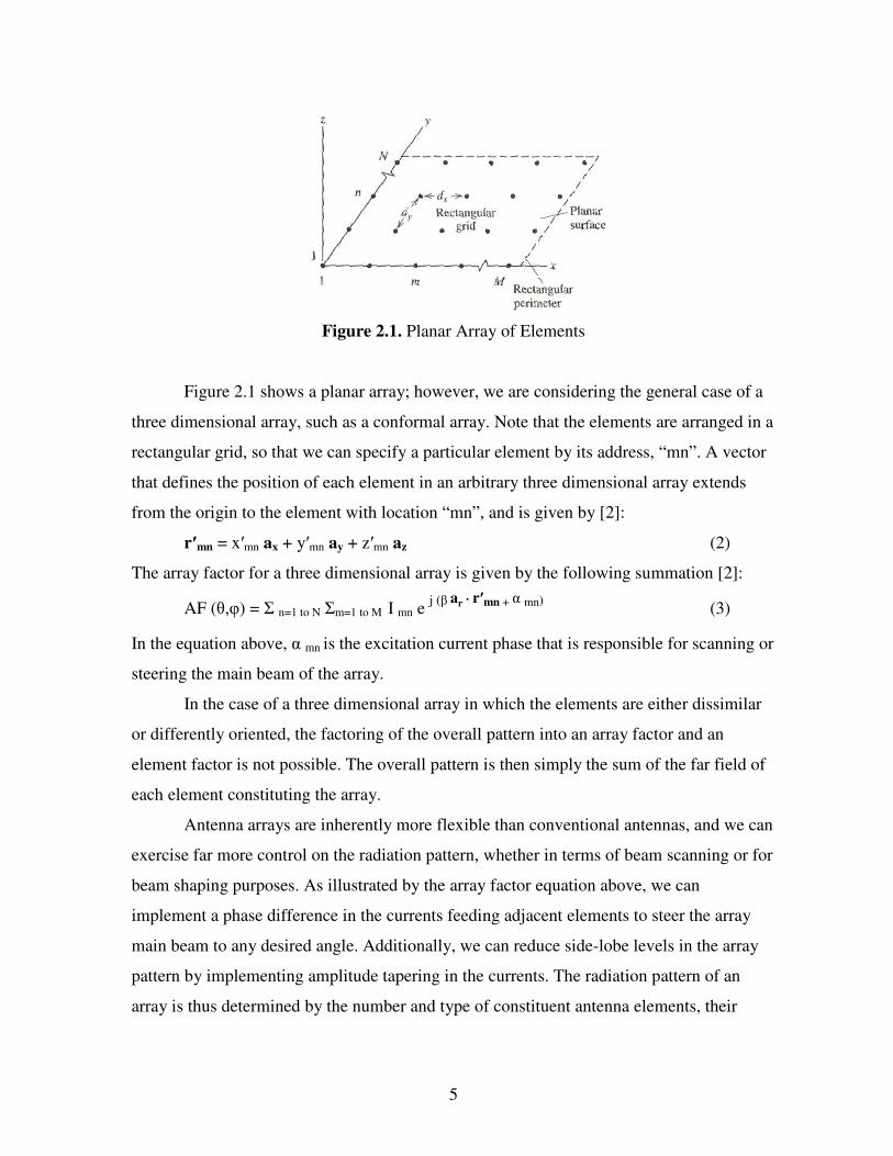
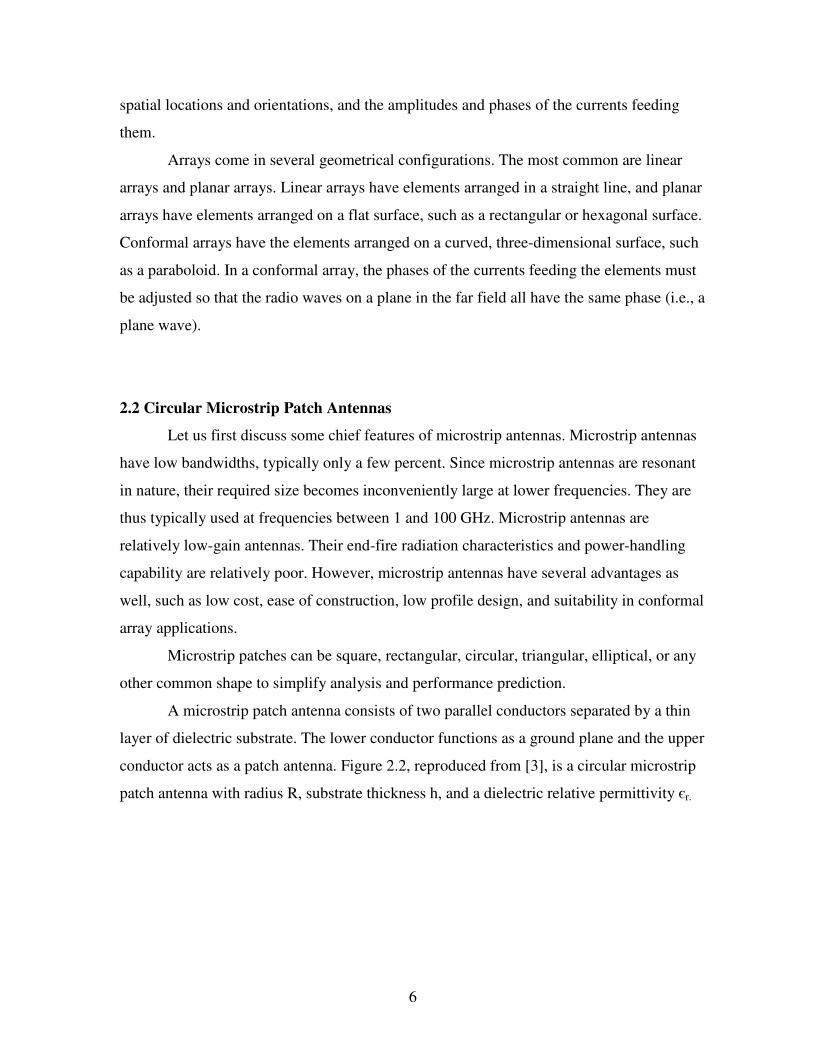
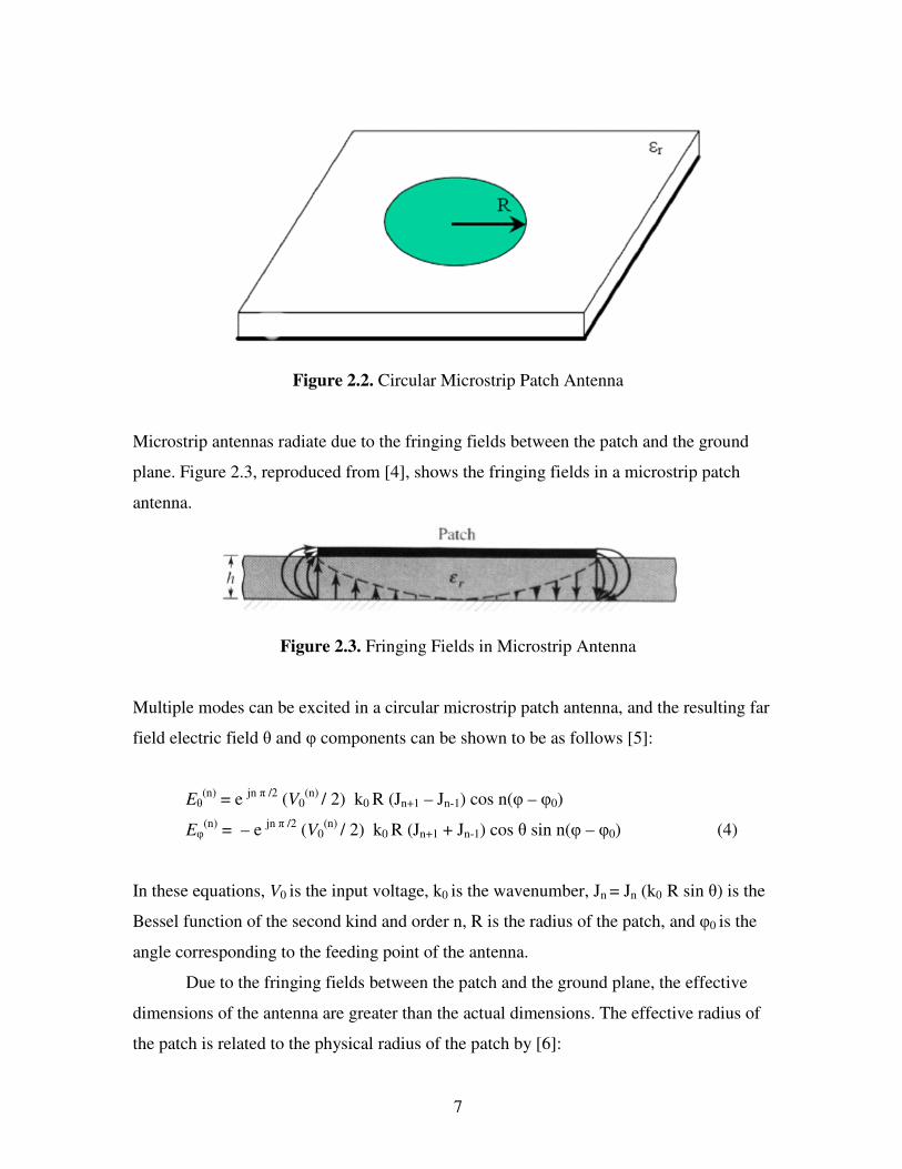
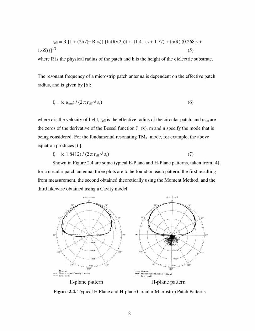
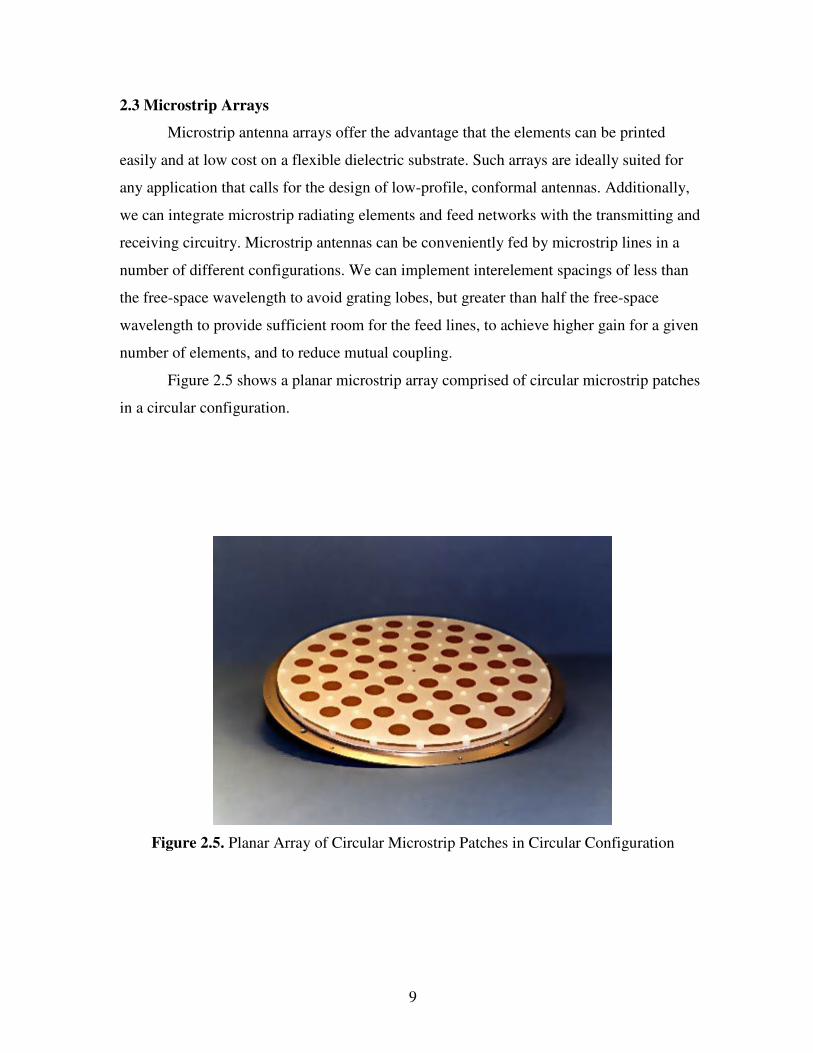
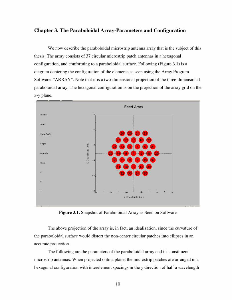
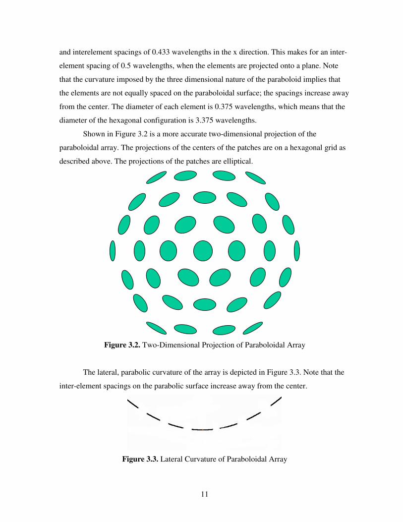
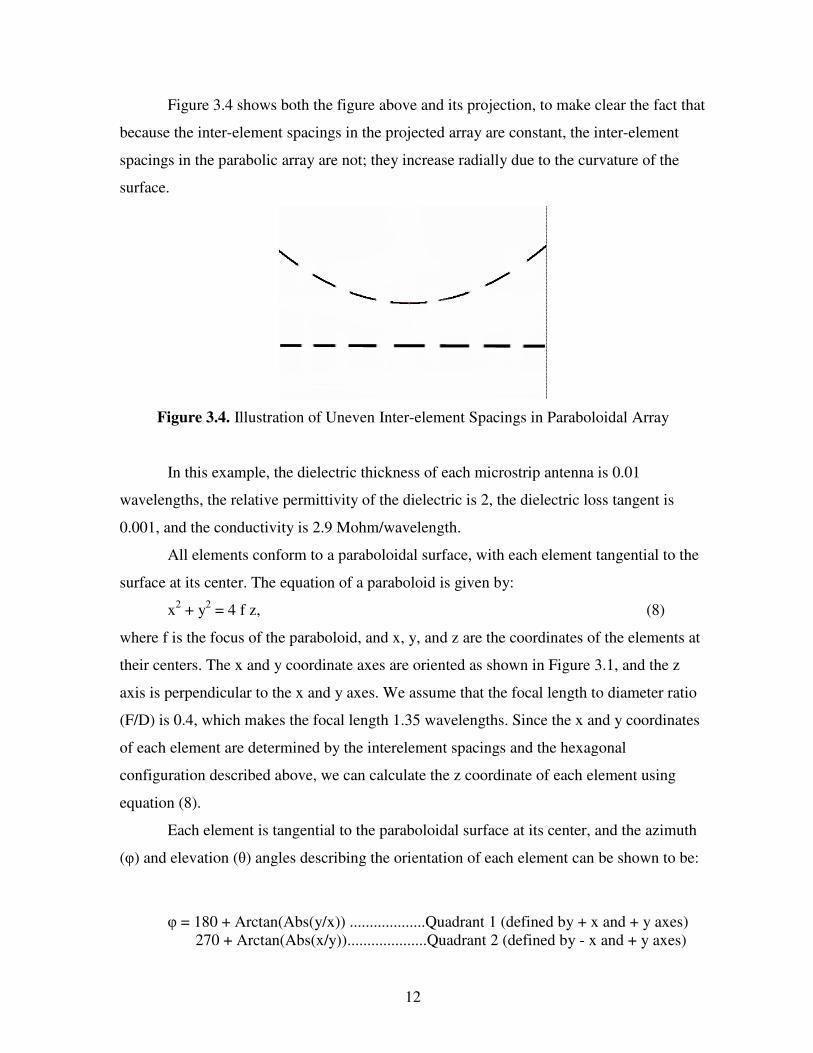
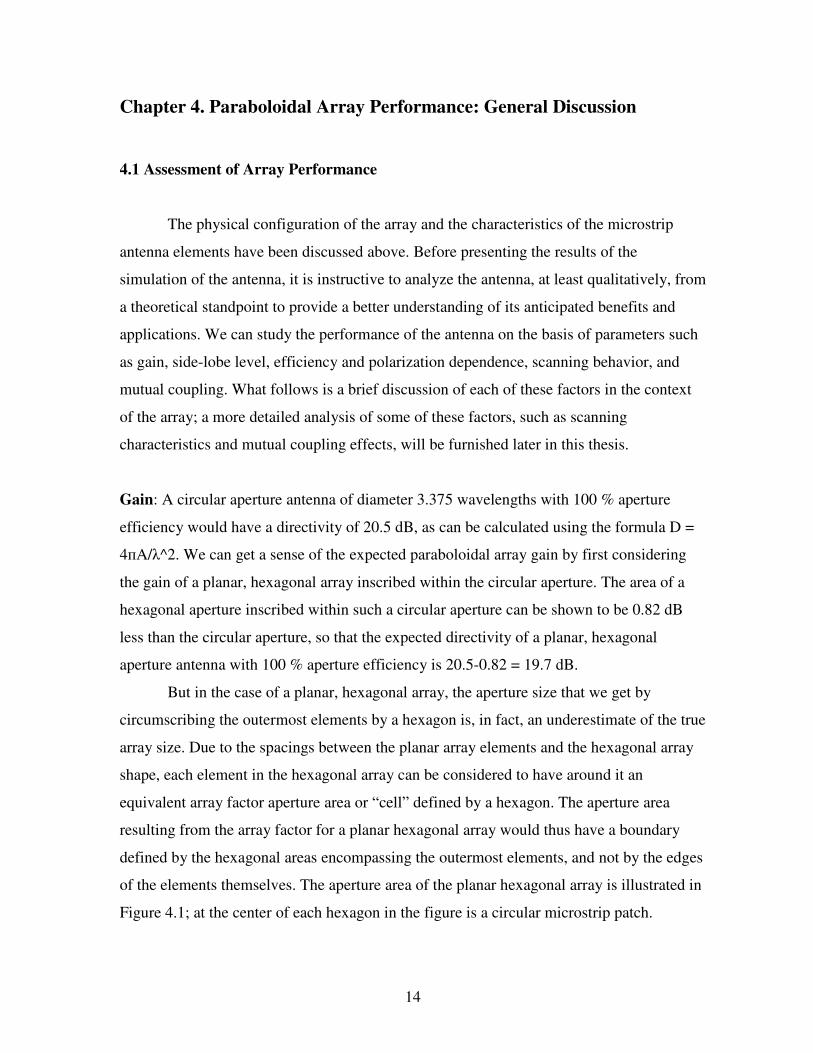
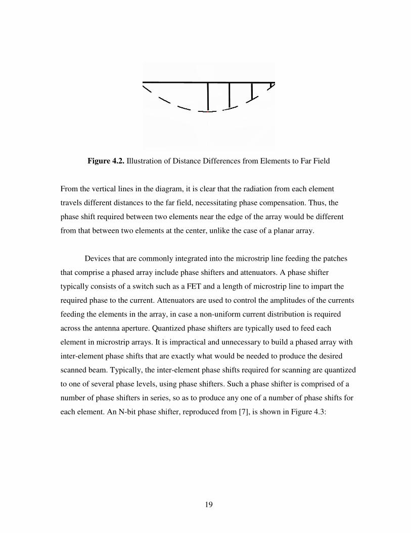
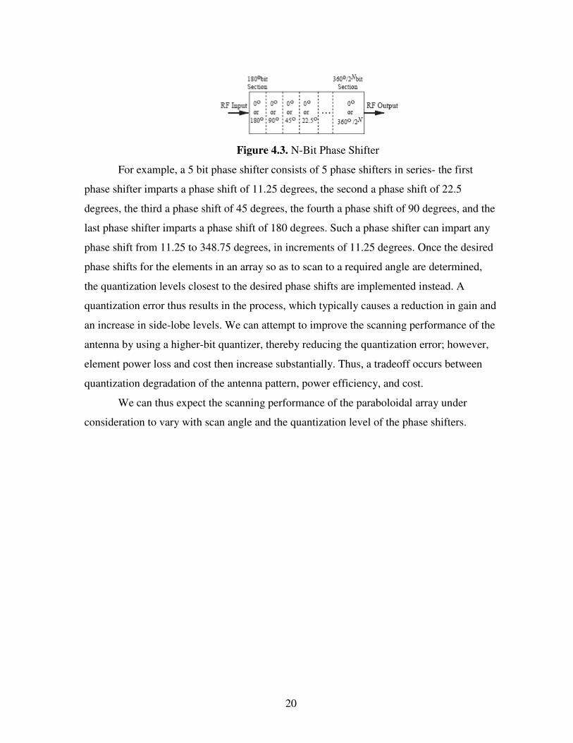
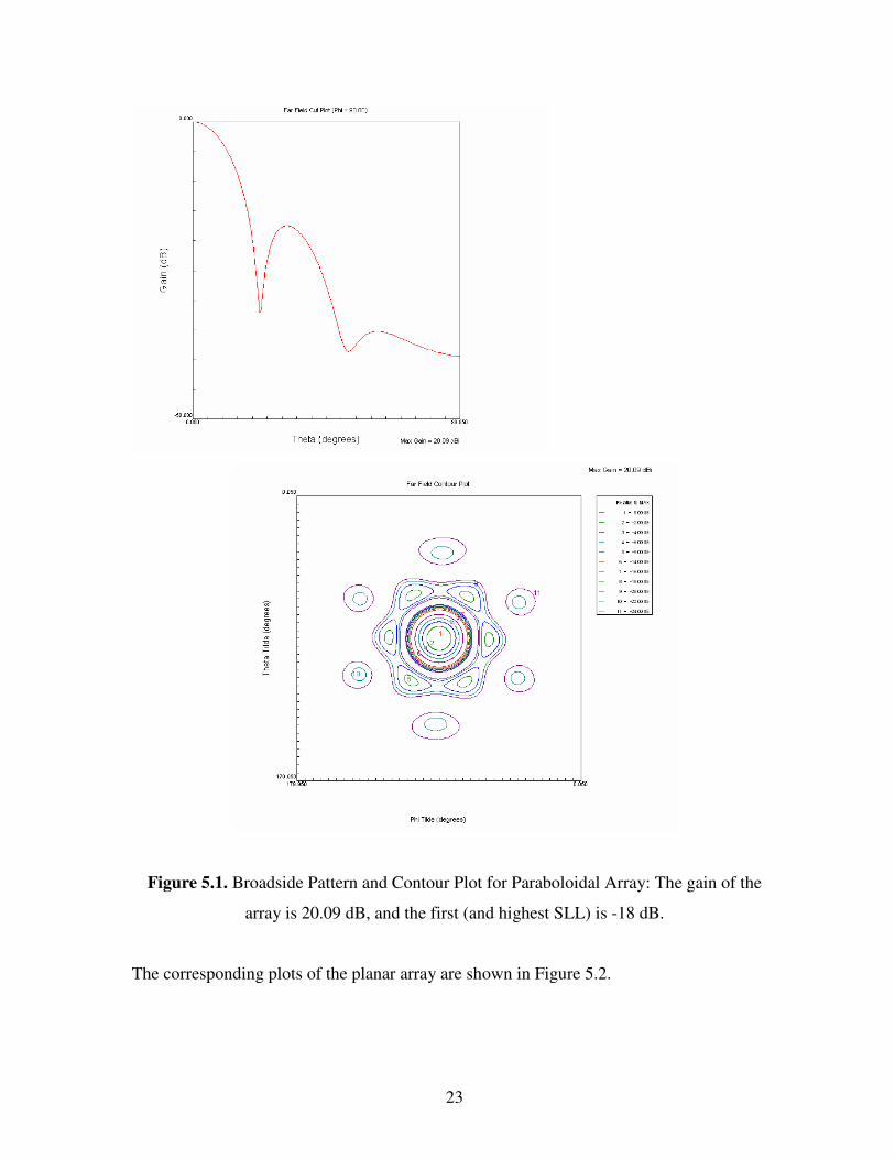
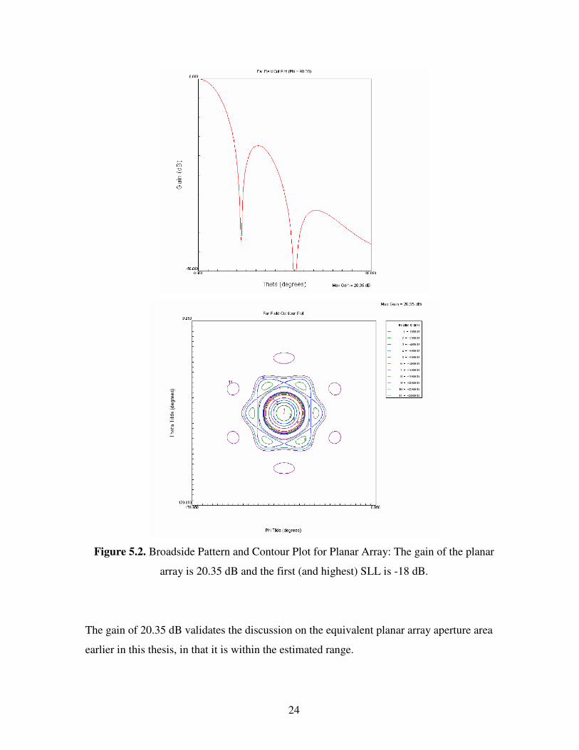
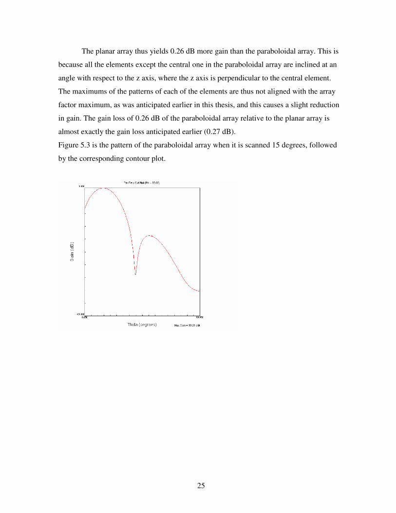
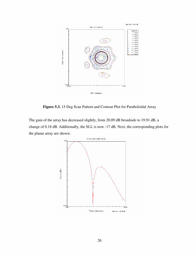
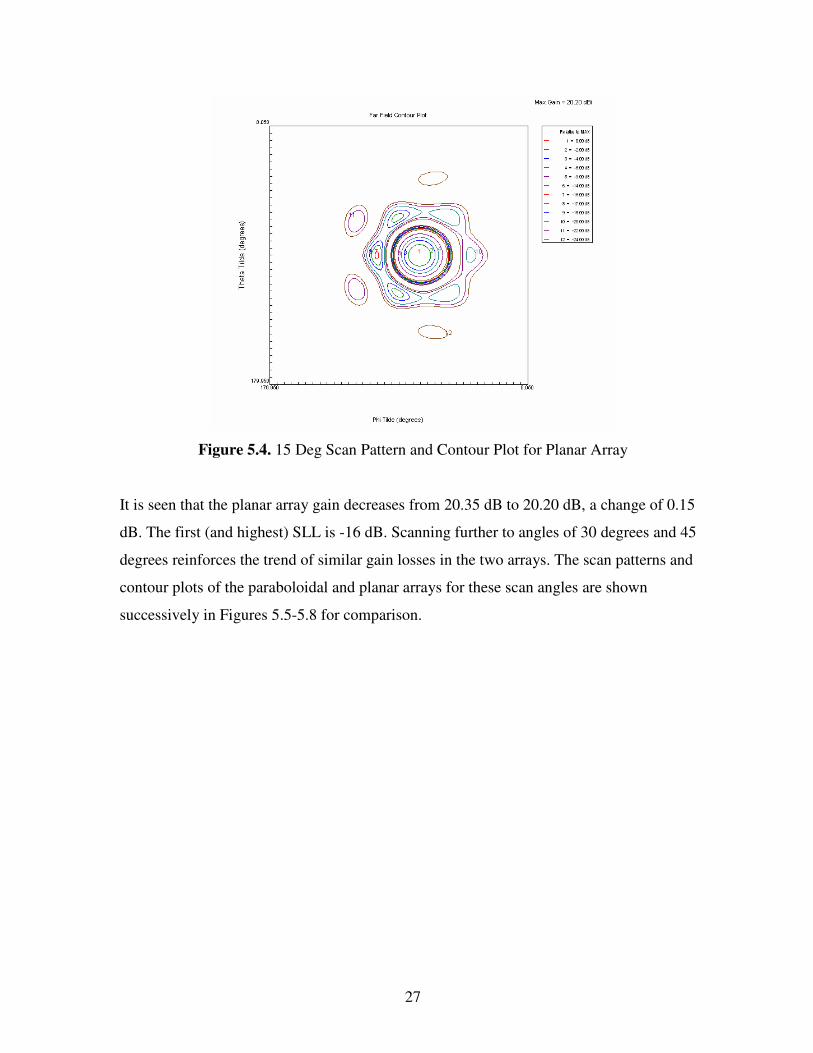
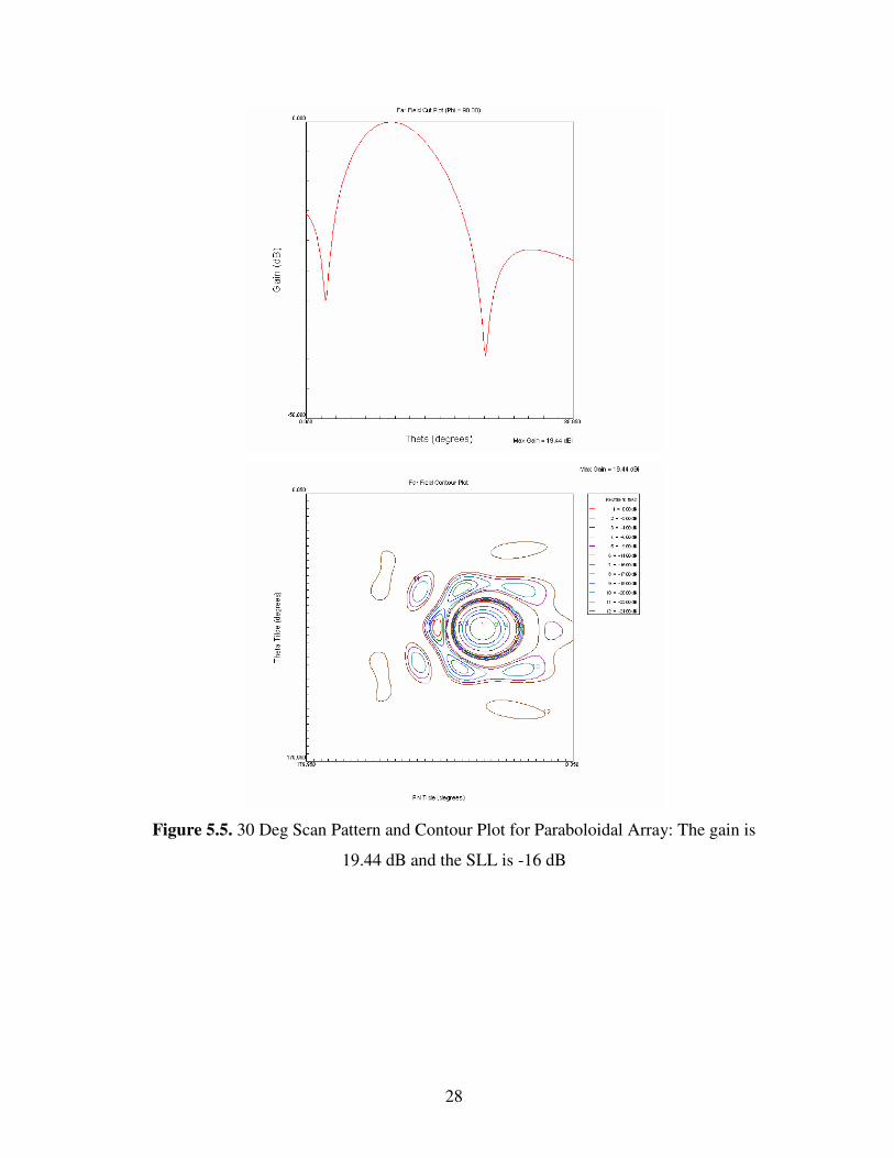
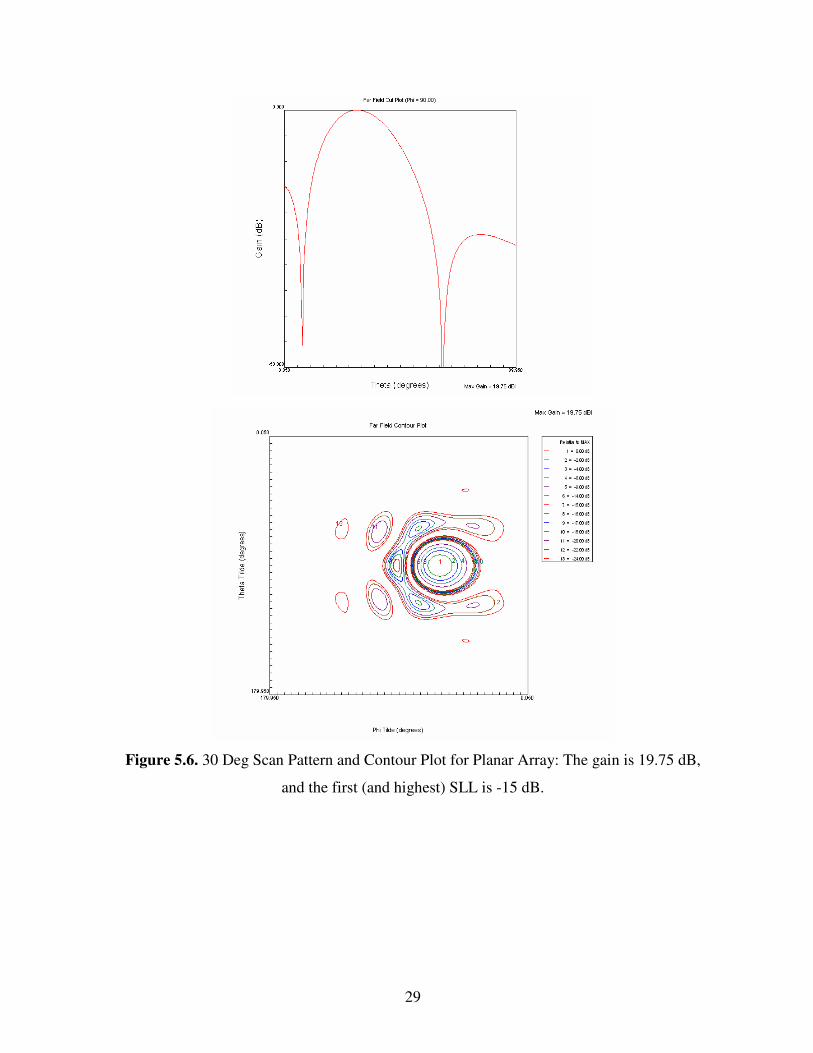
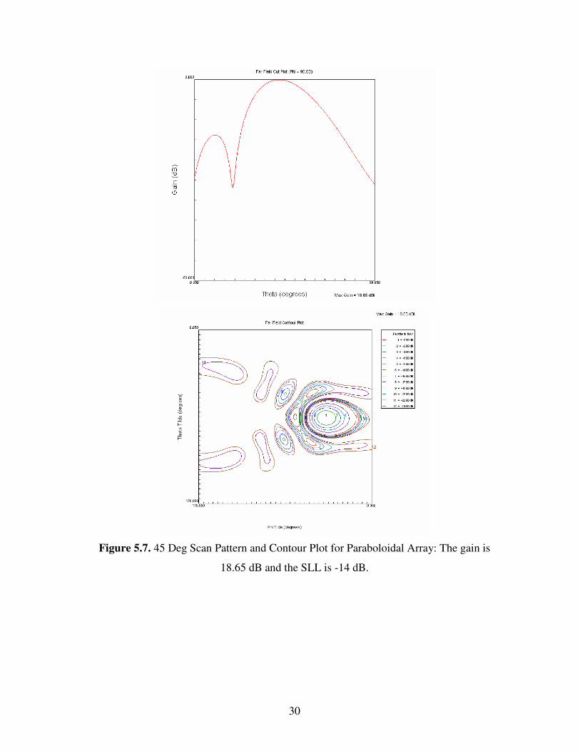
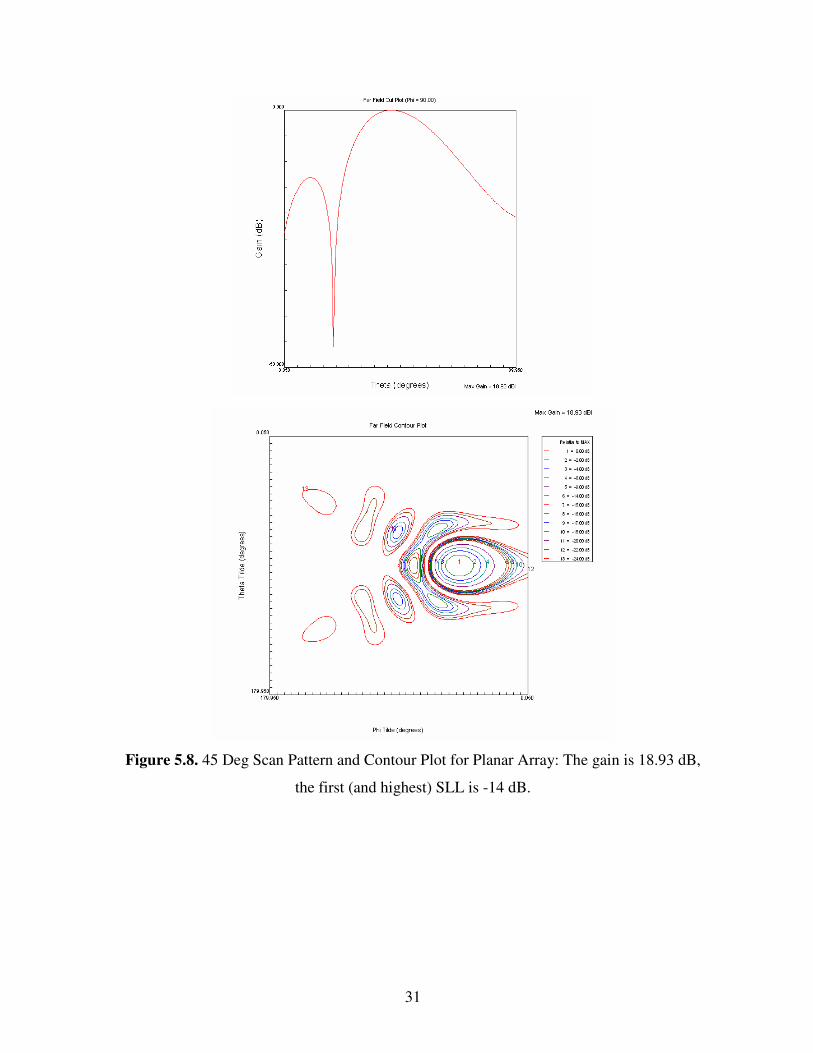
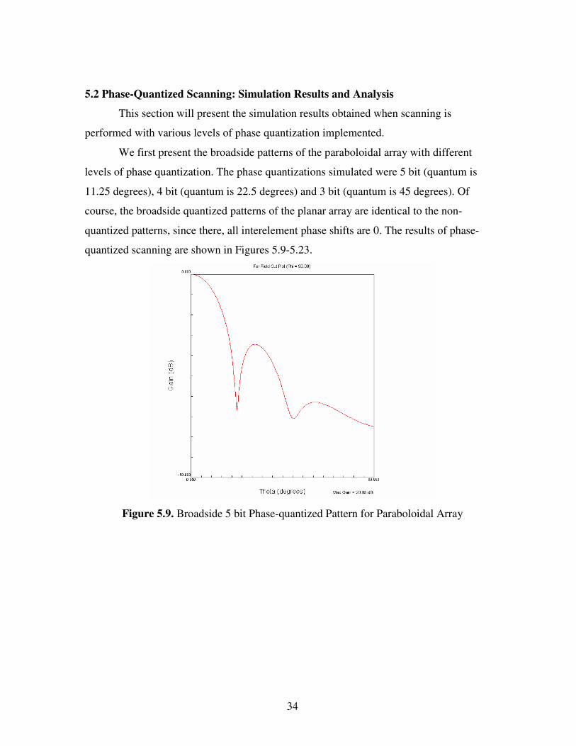
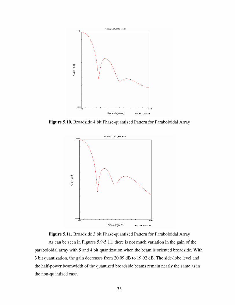
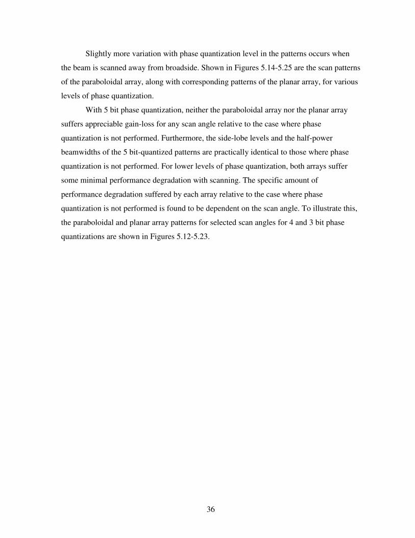
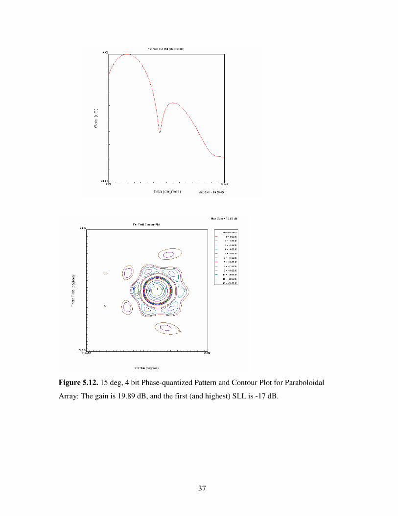
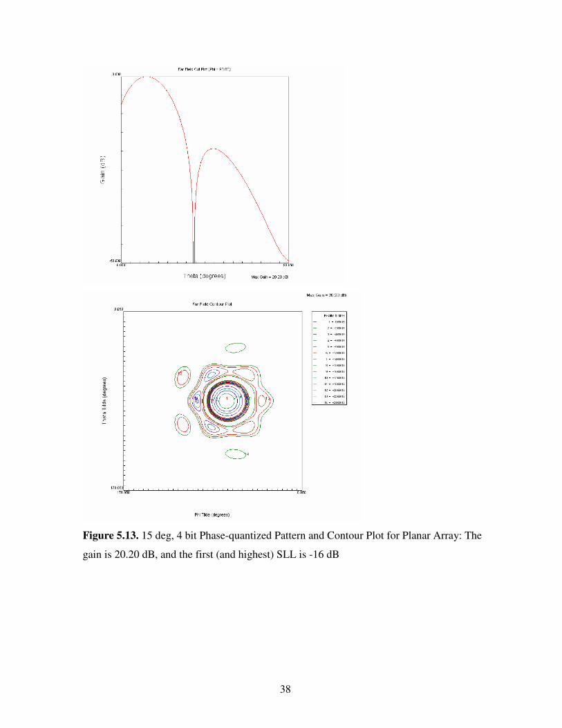
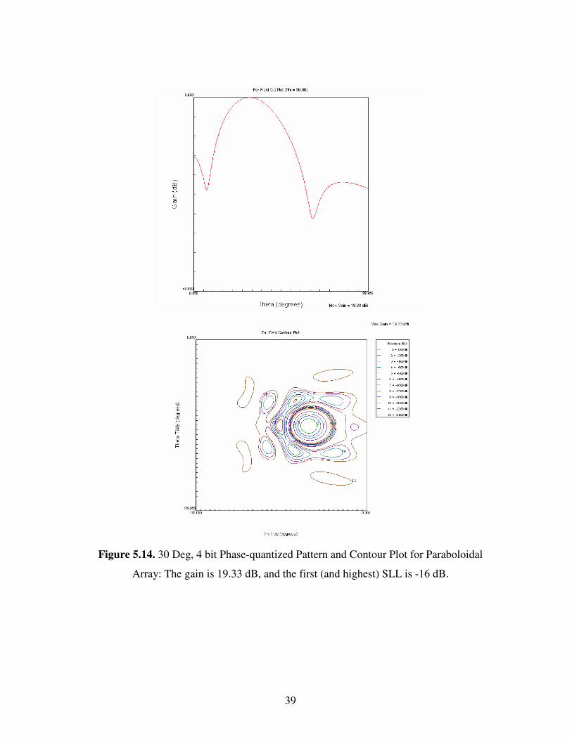
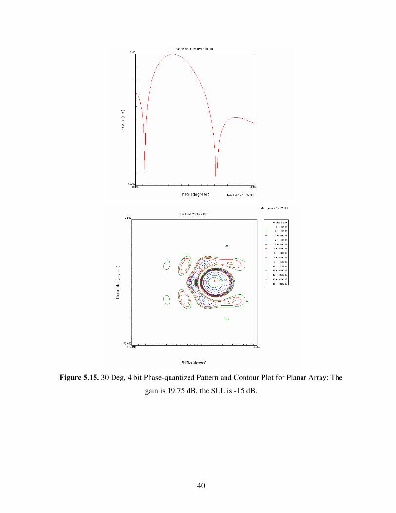
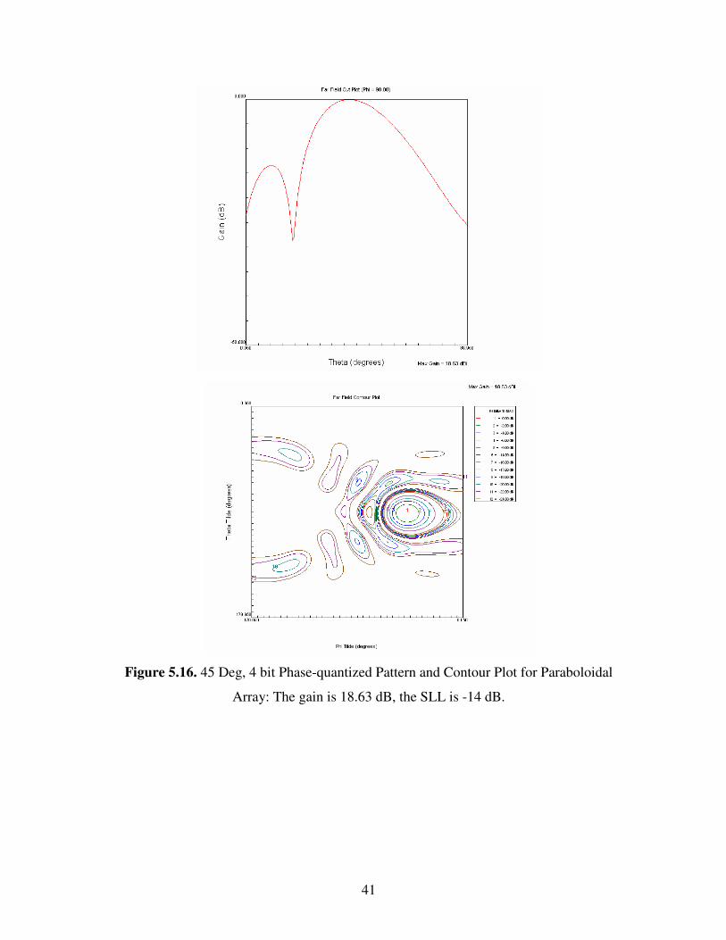
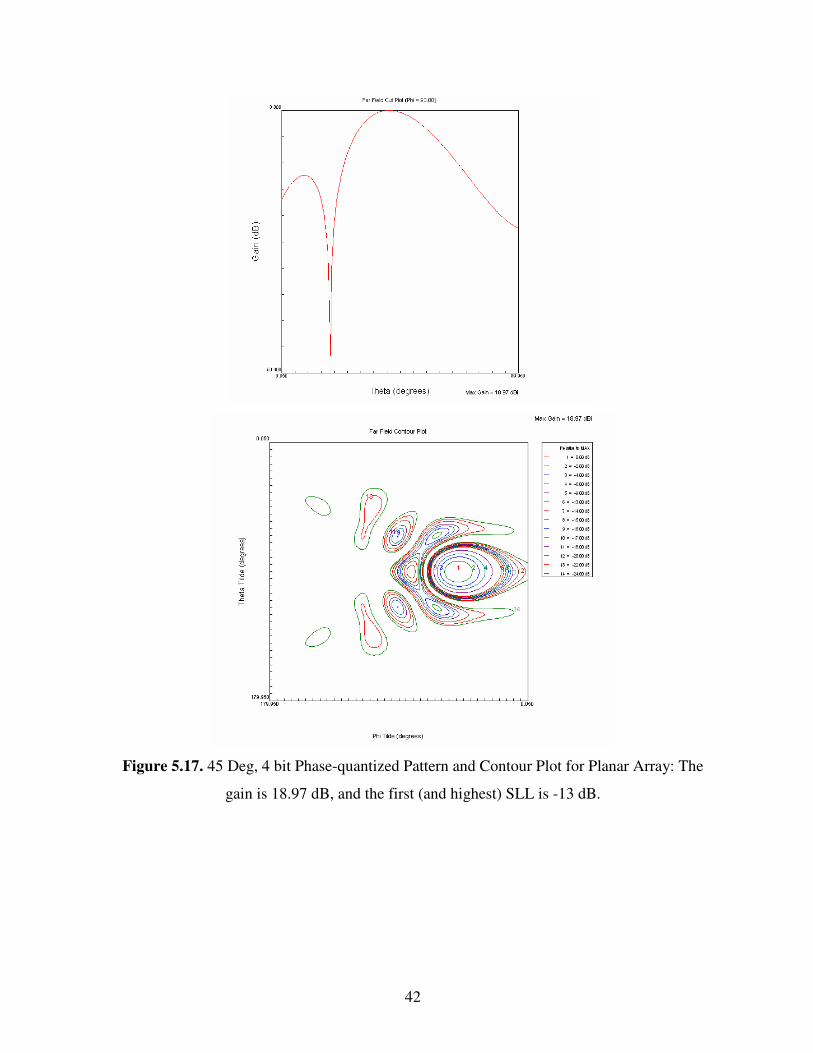
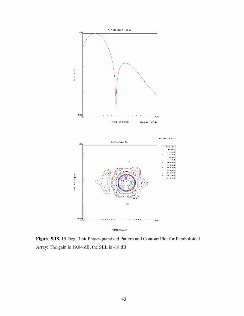
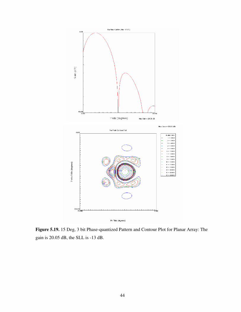
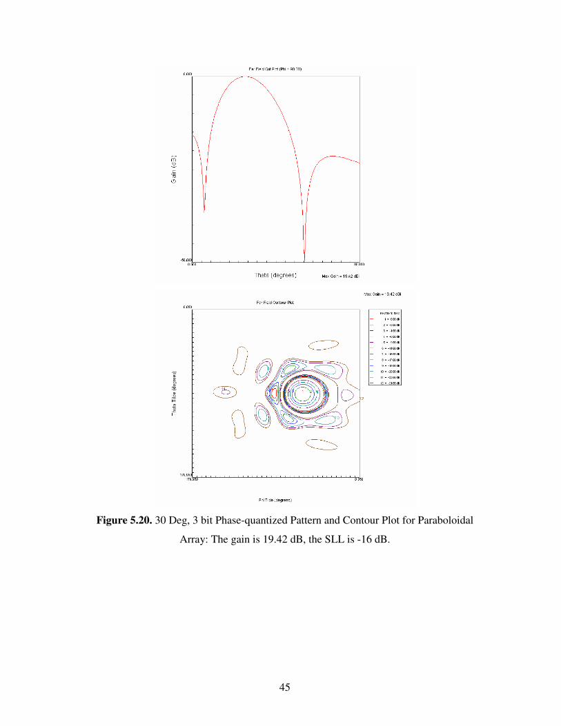
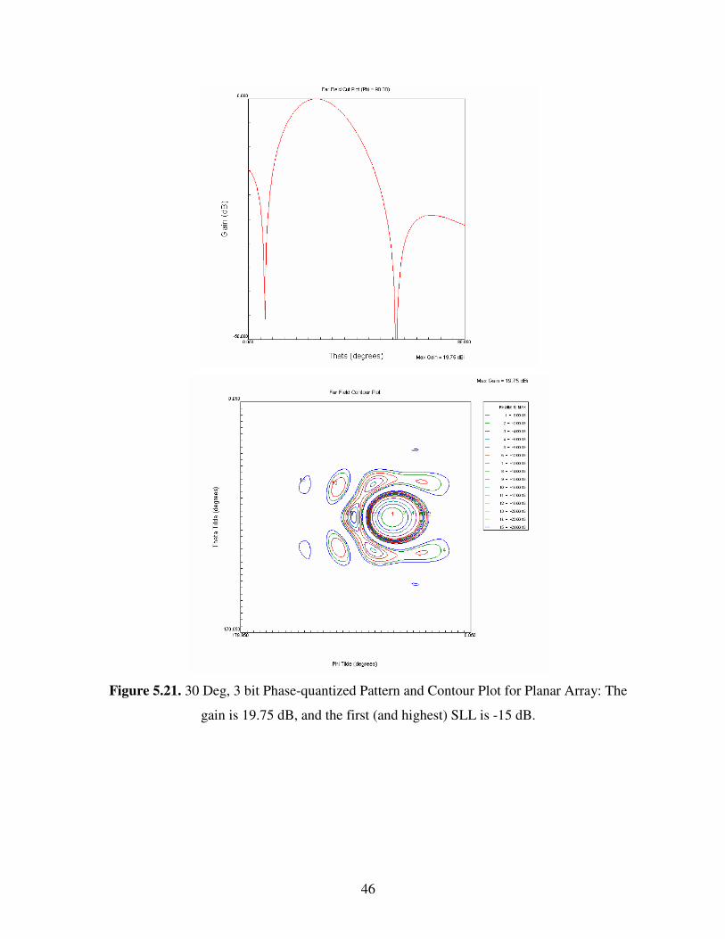
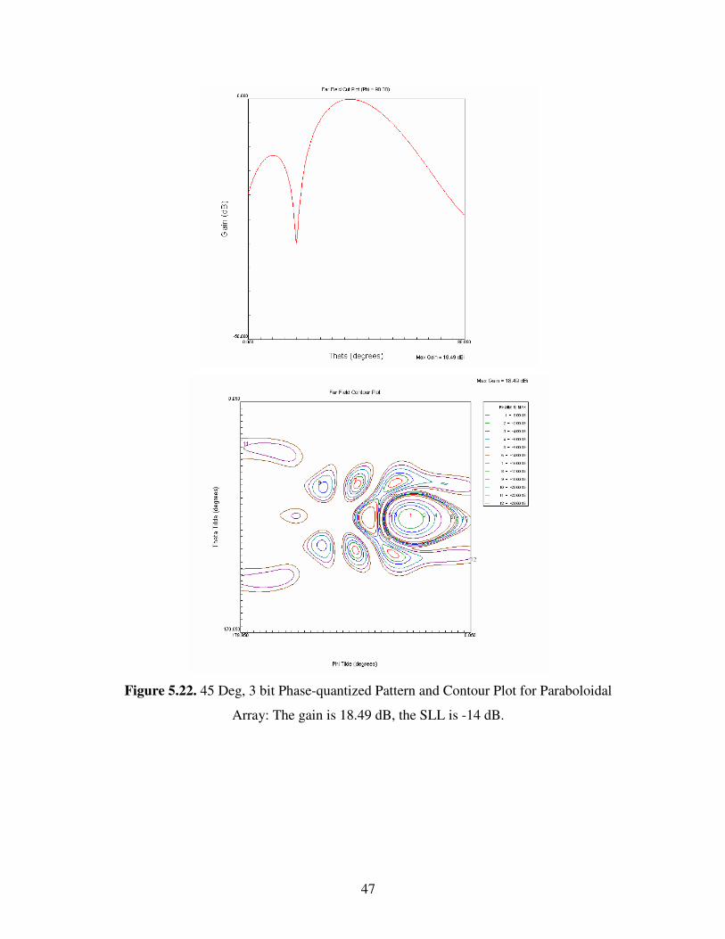
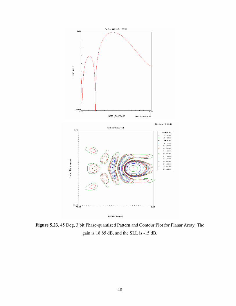
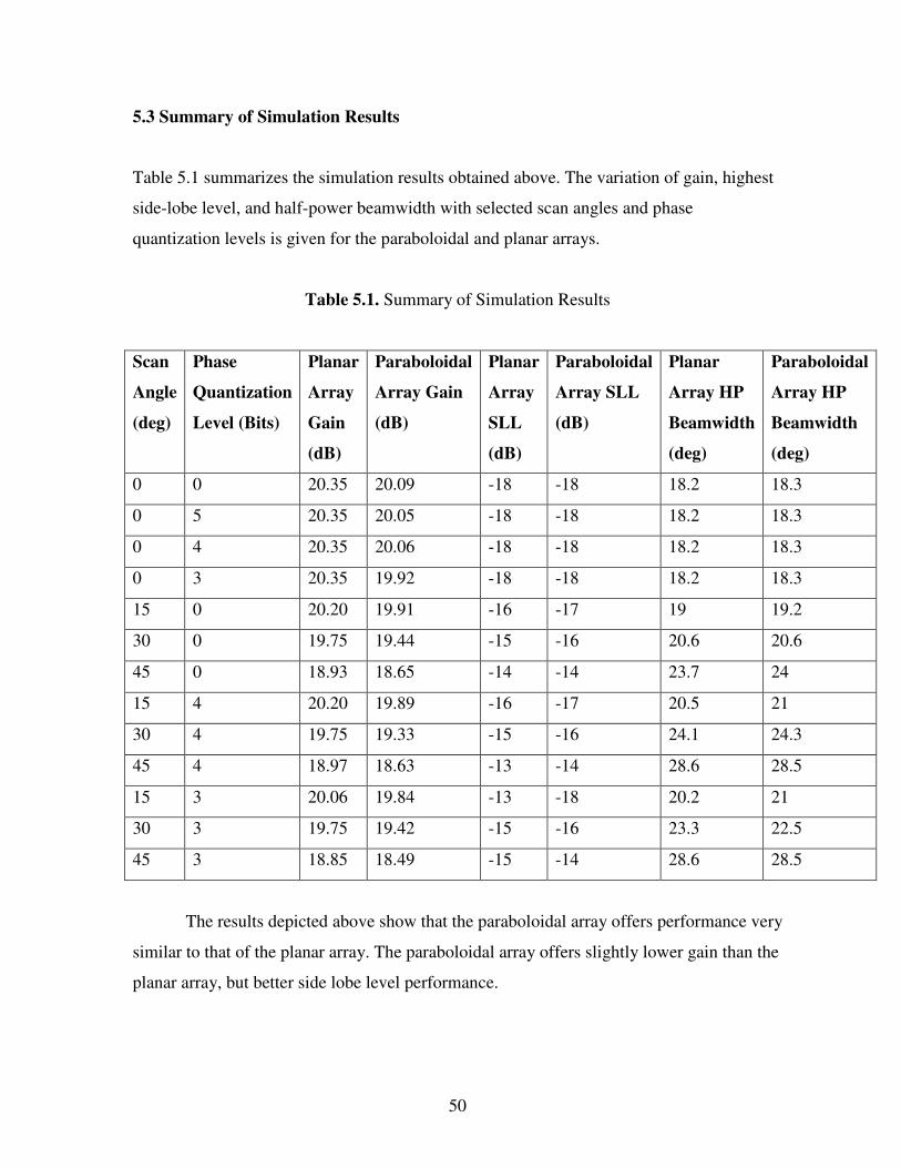
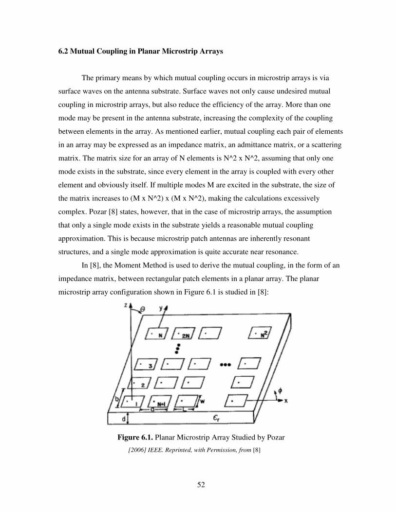
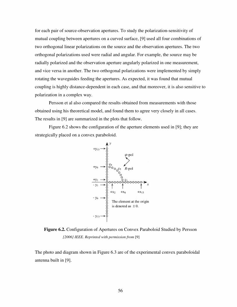
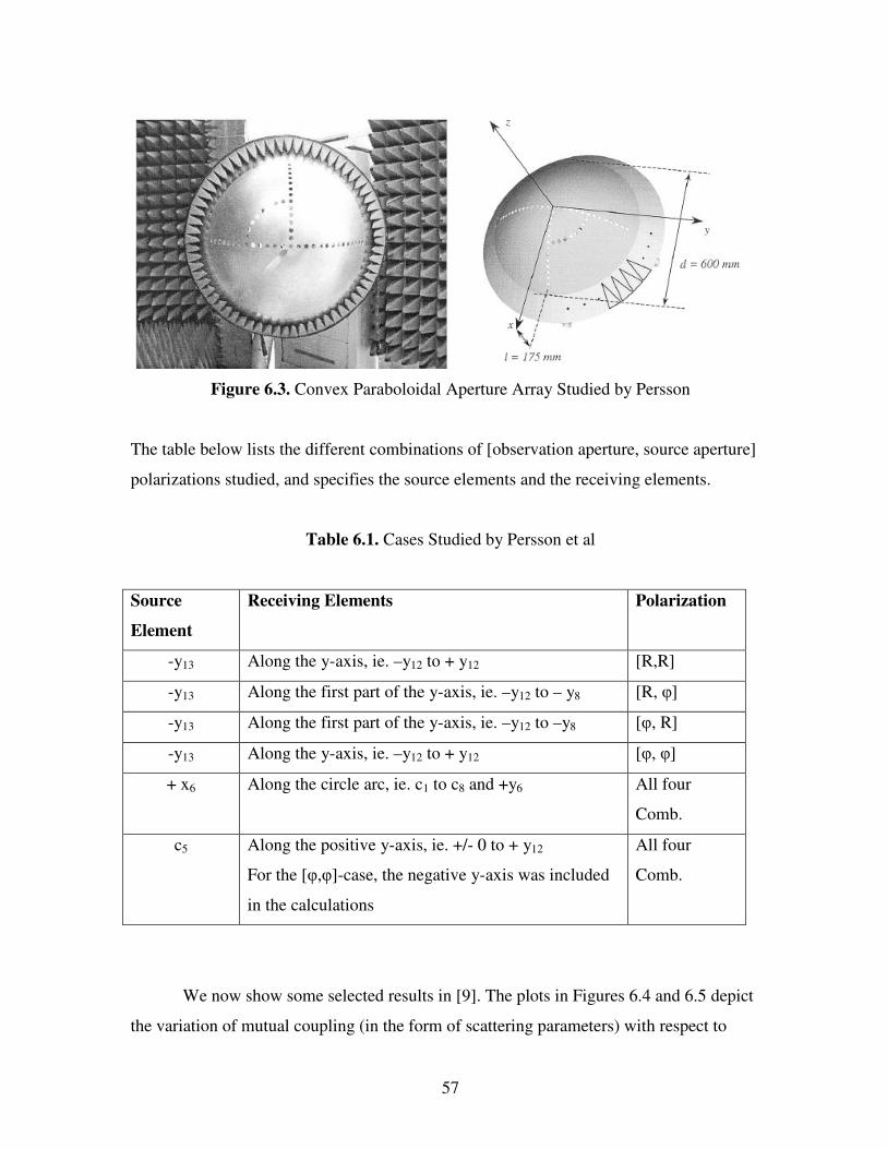
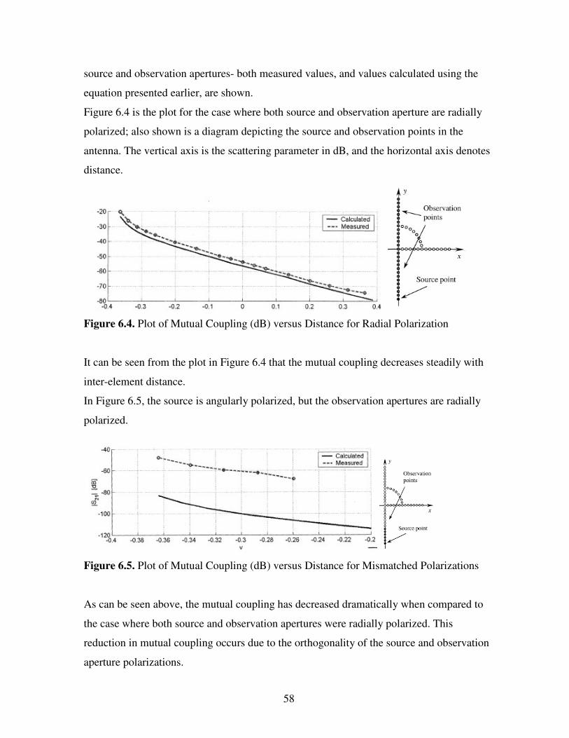
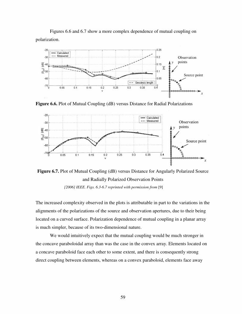
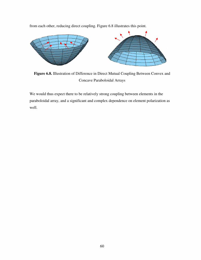
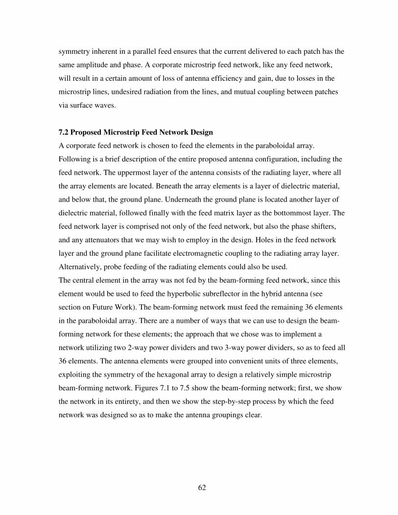
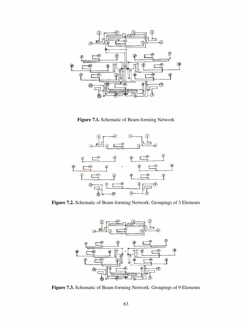
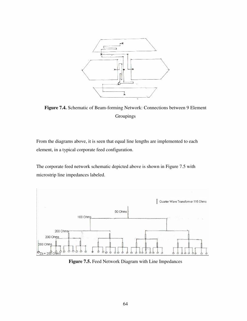