Embed Size (px)
Citation preview

NANOSYSTEMS: PHYSICS, CHEMISTRY, MATHEMATICS, 2021, 12 (3), P. 317–328
Investigation of the effect of zinc precursors onto structural, optical and electricalproperties of CBD deposited ZnS thin films
Rajeshkumar P Khatri1, Amitkumar J Patel2
1Department of Physics, Gujarat Technological University, Ahmedabad 382424, Gujarat, India2Department of Applied Science, Faculty of Physics, Government Engineering College, Godhra,
Panchmahal 389001, Gujarat, India
rajukhatri [email protected]
DOI 10.17586/2220-8054-2021-12-3-317-328
Zinc sulfide (ZnS) thin films were deposited onto microscopic silica slides through the cost-effective chemical bath deposition (CBD) method.The optimized bath parameters were: 25 ml of 0.1 M zinc precursors (ZnCl2, Zn(CH3COO)2, ZnSO4), 25 ml of 1 M thiourea and 3 ml of3.75 M triethanolamine (TEA). The effects of different zinc precursors (ZnCl2, Zn(CH3COO)2, ZnSO4) on the growth mechanism of ZnS thinfilm were investigated using thermal, structural, morphological, optical and electrical studies. The XRD pattern has shown Miller indexing peakscorresponding to the hexagonal phase of as-grown ZnS thin film with the estimated grain size of 22 – 27 nm. The change in physical properties(weight loss) of ZnS powder as a function of temperature was recorded using thermogravimetry (TGA/DTA). Scanning electron microscopy (SEM)revealed the effect of ZnCl2, Zn(CH3COO)2 and ZnSO4 precursors on growth mechanism. UV/visible optical transmission/absorption spectradisplayed the transmittance between 10 to 29 % of as-grown ZnS thin film with a band gap in the range of 4.10 – 4.25 eV. Photoluminescence (PL)analyses demonstrated broad blue emission around ∼ 459 nm was attributed to recombination of electron-hole pair from donor-acceptor trap levelsto valance band. Raman spectra of ZnS powder prepared using different zinc precursors were also reported. The values of electrical parameters(resistivity, conductivity, activation energy, Hall coefficient, carrier concentration, mobility) were investigated using the two-point probe methodand Hall-effect apparatus.
Keywords: ZnS thin films, chemical bath deposition, zinc precursors.
Received: 20 January 2021
Revised: 22 April 2021
Final revision: 26 May 2021
1. Introduction
Zinc sulfide (ZnS) is the most promising material in the field of sensors [1], solar cell [2] and bio-imaging [3]. Itis a wide band gap semiconductor that serves as host materials for various kinds of dopant for luminescence applica-tion [4]. In view of the above technological importance, several researchers have made efforts to tailor the physicalproperties of ZnS thin films using variation in thickness [5], molar concentration [6], heat treatment [7], bath temper-ature [8] and other possible means. Earlier, M. Cao, et al. [9] and T. Liu, et al. [10] investigated the effect of differentzinc salts on crystallographic, morphology and optical properties of CBD deposited ZnS thin films. In earlier reportedliteratures, there has not been enough investigation with the effect of zinc precursors on the physical properties of ZnSthin films.
ZnS thin film has been developed by various researchers using different chemical and physical deposition methodssuch as Thermal evaporation [11], Metal-organic chemical vapor deposition (MOCVD) [12], Successive ionic layeradsorption and reaction (SILAR) [13], Chemical bath deposition [14], etc. Among these deposition methods, CBD issimple, cost-effective and ideal for large scale deposition [15]. Using this CBD method, a thin film can be depositednearly at room temperature through a controlled chemical reaction.
In the present work, authors have tried to deposit CBD-ZnS thin film using triethanolamine (TEA) as a complexingagent since it is a much safer alternative compare to hydrazine hydrate [16]. Moreover, the researchers have investi-gated the effect of different zinc precursors (ZnCl2, Zn(CH3COO)2, ZnSO4) on structural, morphological, optical andelectrical properties of CBD deposited ZnS thin films.

318 Rajeshkumar P Khatri, Amitkumar J Patel
2. Experimental method
All reagents were received from Fisher Scientific and used without further processing. A high-quality silicaslide having dimensions 75 × 26 × 1 mm3 is used as substrate. The cleaning procedure and detailed process of filmdeposition are reported in our earlier literature [17]. The only difference in the present work is that we deposited threedifferent samples using three different precursors instead of zinc chloride, as reported in earlier work. The optimizedmolar concentration and volume of precursors for the growth of ZnS thin films are listed in Table 1. The pre-cleanedsilica substrate is inserted vertically into the reaction bath. The bath temperature was adjusted to 70 C and depositionwas carried for 2 hours. The simplified layout of the chemical bath deposition method is represented in Fig. 1.
TABLE 1. Molar concentration and volume of precursors for the growth of ZnS thin films by CBD method
Thin filmMolar concentration and volume of precursors
zinc precursor thiourea Triethanolamine (TEA) Ammonia
ZnS–Cl 25 ml of 0.1 M ZnCl2 25 ml of 1 M 3 ml of 3.75 M 2 ml of 13.4 M
ZnS–Ac 25 ml of 0.1 M Zn(CH3COO)2 25 ml of 1 M 3 ml of 3.75 M 2 ml of 13.4 M
ZnS–SO 25 ml of 0.1 M ZnSO4 25 ml of 1 M 3 ml of 3.75 M 2 ml of 13.4 M
FIG. 1. Simplified layout of Chemical Bath Deposition Method
After the deposition, the film is taken out from the bath and dipped into de-ionized water to remove loosely boundZnS powder that adheres to the film. ZnS thin films deposited using ZnCl2, Zn(CH3COO)2 and ZnSO4 were labeledas ZnS–Cl, ZnS–Ac and ZnS–SO, respectively for the sake of analysis.
The deposited ZnS thin films were analyzed using various instruments without annealing treatment. The alterationin physical properties as a function of temperature was obtained using thermogravimetry (METTLER TOLEDO). TheMiller indices (h k l) for diffracting planes for the given structure of the thin film was evaluated by grazing incidentX-ray diffraction (GIXRD) spectrometer (PANalytical Empyrean) using CuKα radiations (wavelength = 0.15406 nm)for 2θ values over 20 – 60. X-ray was impinging at angle 0.5 and a detector was moving in the step of 0.01
with a collection time of 7 s. The surface morphology was characterized using the field emission scanning electronmicroscope (JEOL JSM-6010LA). The stoichiometric composition of films was analyzed by energy dispersive X-ray analysis (EDX) using an EDX detector which is available as an add-on attachment with the scanning electronmicroscope (JEOL JSM-5610LV) with Inca software. In order to find the permitting light wavelengths for thin films,transmission/reflectance spectra were recorded as a function of wavelengths using UV/VIS/NIR spectrophotometer(Perkin Elmer Lambda 19). The Raman scattering measurement (vibrational phonon modes) was investigated atroom temperature using a Raman microscope (RENISHAW Invia) with 514 nm (20 mW) argon ion excitation source.Photoluminescence spectra were registered with Perkin Elmer spectro-fluoro-photometer using 280 nm excitationwavelength. A self-made two probe resistivity measurement equipment and Hall-effect apparatus were used to findthe correlation between different electrical parameters.

Investigation of the effect of zinc precursors onto structural, optical and electrical properties... 319
3. Results and discussion
3.1. Thermal analysis
In order to perform thermal analysis of the obtained samples, the as-deposited ZnS powders are collected byscratching the surface of deposited silica substrates. The analysis of the thermal behavior of scratched as-depositedZnS powders were carried out using differential thermal analysis (DTA) and thermogravimetric analysis (TGA) inan ambient environment with temperature in the range of 30 – 900 C. During measurements, the temperature wasincreased at a rate of 30 C/min. DTA and TGA curves for ZnS–Cl, ZnS–Ac, and ZnS–SO powder are shown inFig. 2.
FIG. 2. TGA and DTA curves for ZnS powders grown by CBD method using different zinc precur-sors: (a) ZnS–Cl; (b) ZnS–Ac (c) ZnS–SO
The TGA curve indicates that all the as-grown samples of ZnS lose weight from 30 to 150 C as a result ofabsorbed water vapor evaporation. The decomposition of residual organics and TEA leads to second weight lossbetween 150 – 450 C. It is also confirmed by a series of endothermic peaks between temperature ranges 150–450 Cin DTA sketches, as shown in Fig. 2. The endothermic peak at 615 C in the case of ZnS–Cl and 656 C in the case ofZnS–SO could be attributed to the evaporation of excess residual sulfur ions from the sample [18].
3.2. Structural analysis
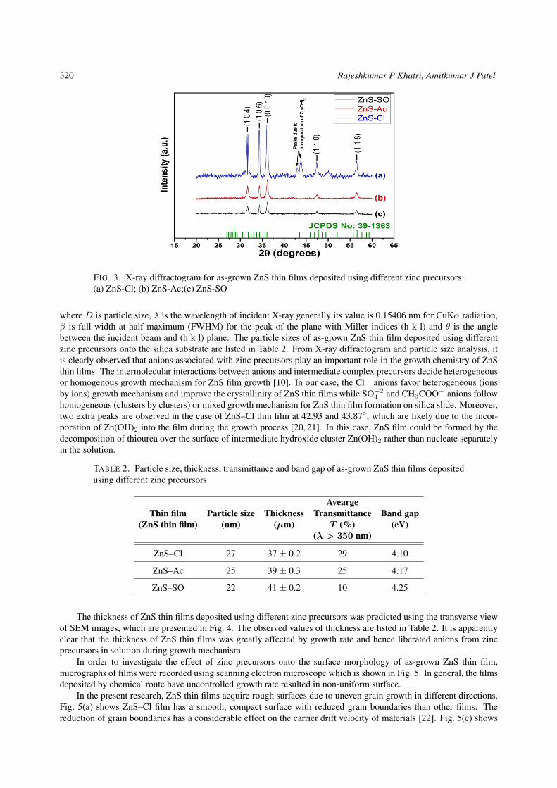
The structural information of ZnS thin film was obtained using grazing incident X-ray diffraction (GIXRD) withCuKα radiation with scan range 20 – 60. GIXRD can reduce the signal contribution from the substrate and improvethe signal from the thin film. X-ray diffractogram of as-grown ZnS thin film prepared using different zinc precursors(ZnCl2, Zn(CH3COO)2 and ZnSO4) are shown in Fig. 3.
The peaks at 2θ values 31.64, 34.53, 36.20, 47.45 and 56.48 are diffraction angles for planes with Millerindices (1 0 4), (1 0 6), (0 0 10), (1 1 0) and (1 1 8) which satisfies Bragg’s equation. The plane (0 0 10) consists morenumber of atoms resulted in the highest intensity peak. Comparing observed peaks with JCPDS card No. 39-1363assures hexagonal phase of ZnS thin film.
The particle size of ZnS thin films deposited using different zinc precursors were calculated using the Debye–Scherrer formula as [19]:
D =0.94λ
β cos θ, (1)
320 Rajeshkumar P Khatri, Amitkumar J Patel
FIG. 3. X-ray diffractogram for as-grown ZnS thin films deposited using different zinc precursors:(a) ZnS-Cl; (b) ZnS-Ac;(c) ZnS-SO
where D is particle size, λ is the wavelength of incident X-ray generally its value is 0.15406 nm for CuKα radiation,β is full width at half maximum (FWHM) for the peak of the plane with Miller indices (h k l) and θ is the anglebetween the incident beam and (h k l) plane. The particle sizes of as-grown ZnS thin film deposited using differentzinc precursors onto the silica substrate are listed in Table 2. From X-ray diffractogram and particle size analysis, itis clearly observed that anions associated with zinc precursors play an important role in the growth chemistry of ZnSthin films. The intermolecular interactions between anions and intermediate complex precursors decide heterogeneousor homogenous growth mechanism for ZnS film growth [10]. In our case, the Cl− anions favor heterogeneous (ionsby ions) growth mechanism and improve the crystallinity of ZnS thin films while SO−2
4 and CH3COO− anions followhomogeneous (clusters by clusters) or mixed growth mechanism for ZnS thin film formation on silica slide. Moreover,two extra peaks are observed in the case of ZnS–Cl thin film at 42.93 and 43.87, which are likely due to the incor-poration of Zn(OH)2 into the film during the growth process [20, 21]. In this case, ZnS film could be formed by thedecomposition of thiourea over the surface of intermediate hydroxide cluster Zn(OH)2 rather than nucleate separatelyin the solution.
TABLE 2. Particle size, thickness, transmittance and band gap of as-grown ZnS thin films depositedusing different zinc precursors
Thin film(ZnS thin film)
Particle size(nm)
Thickness(µm)
AveargeTransmittance
T (%)(λ > 350 nm)
Band gap(eV)
ZnS–Cl 27 37 ± 0.2 29 4.10
ZnS–Ac 25 39 ± 0.3 25 4.17
ZnS–SO 22 41 ± 0.2 10 4.25
The thickness of ZnS thin films deposited using different zinc precursors was predicted using the transverse viewof SEM images, which are presented in Fig. 4. The observed values of thickness are listed in Table 2. It is apparentlyclear that the thickness of ZnS thin films was greatly affected by growth rate and hence liberated anions from zincprecursors in solution during growth mechanism.
In order to investigate the effect of zinc precursors onto the surface morphology of as-grown ZnS thin film,micrographs of films were recorded using scanning electron microscope which is shown in Fig. 5. In general, the filmsdeposited by chemical route have uncontrolled growth rate resulted in non-uniform surface.
In the present research, ZnS thin films acquire rough surfaces due to uneven grain growth in different directions.Fig. 5(a) shows ZnS–Cl film has a smooth, compact surface with reduced grain boundaries than other films. Thereduction of grain boundaries has a considerable effect on the carrier drift velocity of materials [22]. Fig. 5(c) shows

Investigation of the effect of zinc precursors onto structural, optical and electrical properties... 321
FIG. 4. Transverse view of SEM images for as-grown ZnS thin films deposited using different zincprecursors: (a) ZnS-Cl; (b) ZnS-Ac; (c) ZnS-SO
FIG. 5. SEM micrograph of as-grown ZnS thin films deposited using different zinc precursors: (a)ZnS-Cl; (b) ZnS-Ac; (c) ZnS-SO
ZnS–SO films formed by significant spherical clusters with relatively less dense morphology. The reason for this isSO−2
4 anions promote homogeneous (clusters by clusters) growth mechanism and ZnS clusters from solution adhereon a silica substrate. Fig. 5(b) shows ZnS–Ac film is relatively less compact than ZnS–Cl with flower-like morphology.In this case, CH3COO− anions promote a mixed growth mechanism in the solution for deposition of ZnS thin films.
3.3. Compositional analysis
The elemental composition of ZnS films deposited onto the silica substrate using different zinc precursors wasanalyzed using EDX spectra and is shown in Fig. 6. The obtained results are listed in Table 3. Because of the lowthickness of films and high depth profile of EDX spectrometer, other elements from silica substrate such as O, Mg, Si,and Ca are also detected in the EDX spectra. As seen from Table 3, the atomic ratios of Zn/S are slightly higher than1 which indicates that the obtained ZnS films are rich in zinc and deficient in sulfur. The difference in the Zn/S ratiois ascribed to different growth mechanisms involved during film formation. The presence of excess zinc in the case ofZnS–Cl films could be due to the presence of Zn(OH)2 [9, 10], which is consistent with our XRD results.
TABLE 3. Elemental composition of as-deposited ZnS thin films from EDX spectra
Thin film Zn (at %) S (at %) Other elements (at %) Zn/S atomic ratio
ZnS–Cl 26.22 22.74 51.04 1.15
ZnS–Ac 25.38 22.58 52.04 1.12
ZnS–SO 24.71 22.45 52.84 1.10

322 Rajeshkumar P Khatri, Amitkumar J Patel
FIG. 6. EDX spectra of as-grown ZnS thin films deposited using different zinc precursors: (a) ZnS-Cl; (b) ZnS-Ac; (c) ZnS-SO
3.4. Optical analysis
The thickness and uniformity of film play a vital role in controlling optical properties like transmittance, ab-sorbance, refractive index, etc. [23]. A film with higher uniformity and the least thickness leads to the high transmis-sion with a sharp absorption edge [24]. Moreover, the energy band gap of the film can be determined from transmissionspectra [23].
In the direction to know the effect of zinc precursors on the optical behavior of as-grown ZnS thin films, trans-mittance and reflectance spectra were noted using UV/VIS/NIR spectrophotometer. Fig. 7 shows the percentage oftransmittance and absorbance of CBD-deposited as-grown ZnS thin films with zinc precursor variation. The highesttransmittance is observed in ZnS–Cl thin film and lowest in ZnS–SO thin film. It shows low absorption above 350 nmwavelength and abrupt absorption at ∼ 310 nm wavelength for all ZnS thin films.
FIG. 7. UV/visible transmittance and absorbance spectra of as-grown ZnS thin films deposited us-ing different zinc precursors: (a) ZnS-Cl; (b) ZnS-Ac; (c) ZnS-SO
Once Transmission/Reflectance data were registered with respect to wavelength, the optical energy band gapsof thin films were evaluated with the help of the formula derived from the theory of inter-band transition of the
Investigation of the effect of zinc precursors onto structural, optical and electrical properties... 323
semiconductor. The absorption coefficient (α) was determined from absorbance (A) and film thickness (t) by usingthe relation [25, 26]:
α =2.303 ·A
t. (2)
The theory of inter-band transition shows that at the optical absorption edge, the absorption coefficient (α) varieswith the photon energy hν according to [23]:
αhν = A(hν − Eg)n, (3)
whereEg is the optically forbidden energy gap,A is constant and the exponential factor n = 1/2, 1, 2, 3 depending onthe type of electronic transition in k-space [26]. For direct band gap semiconductor, the exponential factor has value0.5 and for indirect band gap semiconductor, it has a value of 2. Since ZnS is a direct band gap material, the value ofn becomes 0.5:
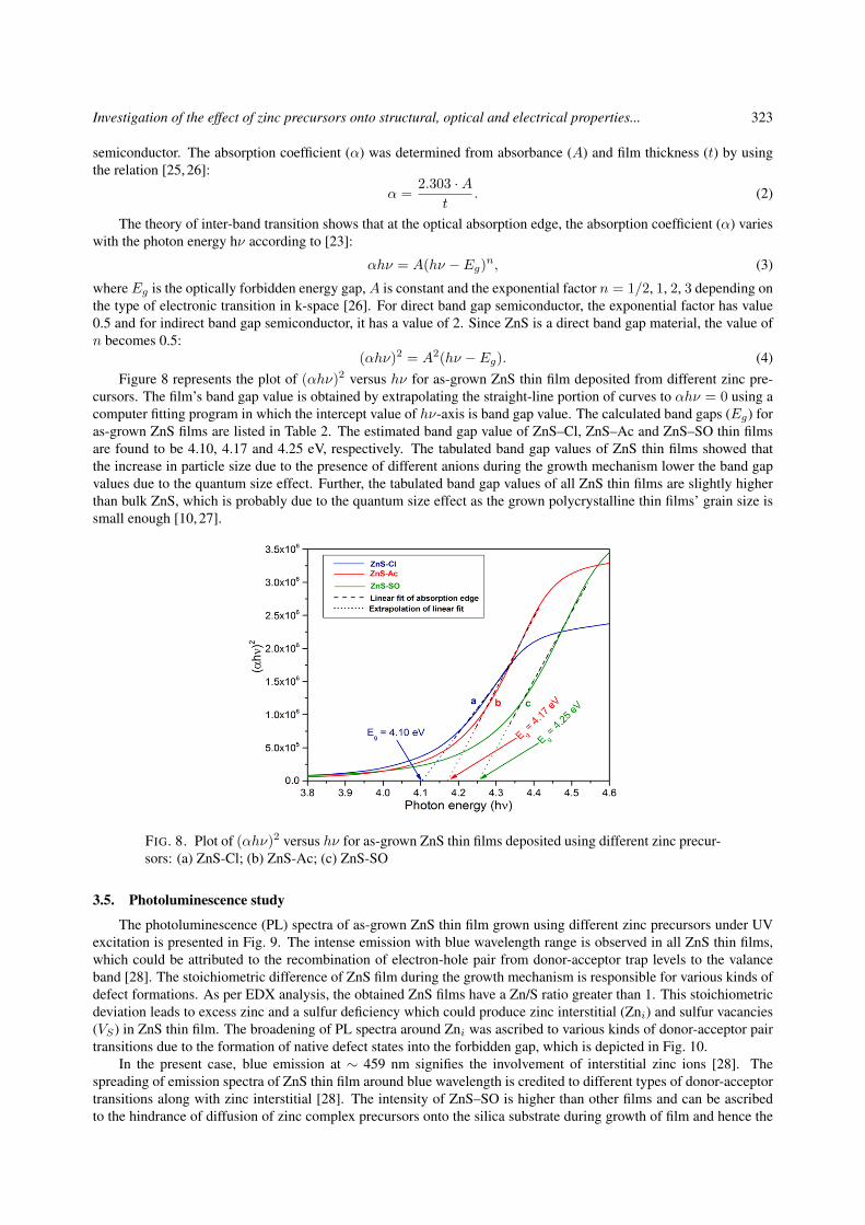
(αhν)2 = A2(hν − Eg). (4)Figure 8 represents the plot of (αhν)2 versus hν for as-grown ZnS thin film deposited from different zinc pre-
cursors. The film’s band gap value is obtained by extrapolating the straight-line portion of curves to αhν = 0 using acomputer fitting program in which the intercept value of hν-axis is band gap value. The calculated band gaps (Eg) foras-grown ZnS films are listed in Table 2. The estimated band gap value of ZnS–Cl, ZnS–Ac and ZnS–SO thin filmsare found to be 4.10, 4.17 and 4.25 eV, respectively. The tabulated band gap values of ZnS thin films showed thatthe increase in particle size due to the presence of different anions during the growth mechanism lower the band gapvalues due to the quantum size effect. Further, the tabulated band gap values of all ZnS thin films are slightly higherthan bulk ZnS, which is probably due to the quantum size effect as the grown polycrystalline thin films’ grain size issmall enough [10, 27].
FIG. 8. Plot of (αhν)2 versus hν for as-grown ZnS thin films deposited using different zinc precur-sors: (a) ZnS-Cl; (b) ZnS-Ac; (c) ZnS-SO
3.5. Photoluminescence study
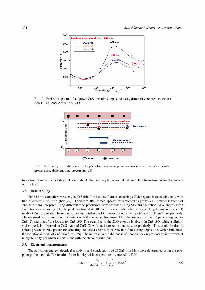
The photoluminescence (PL) spectra of as-grown ZnS thin film grown using different zinc precursors under UVexcitation is presented in Fig. 9. The intense emission with blue wavelength range is observed in all ZnS thin films,which could be attributed to the recombination of electron-hole pair from donor-acceptor trap levels to the valanceband [28]. The stoichiometric difference of ZnS film during the growth mechanism is responsible for various kinds ofdefect formations. As per EDX analysis, the obtained ZnS films have a Zn/S ratio greater than 1. This stoichiometricdeviation leads to excess zinc and a sulfur deficiency which could produce zinc interstitial (Zni) and sulfur vacancies(VS) in ZnS thin film. The broadening of PL spectra around Zni was ascribed to various kinds of donor-acceptor pairtransitions due to the formation of native defect states into the forbidden gap, which is depicted in Fig. 10.
In the present case, blue emission at ∼ 459 nm signifies the involvement of interstitial zinc ions [28]. Thespreading of emission spectra of ZnS thin film around blue wavelength is credited to different types of donor-acceptortransitions along with zinc interstitial [28]. The intensity of ZnS–SO is higher than other films and can be ascribedto the hindrance of diffusion of zinc complex precursors onto the silica substrate during growth of film and hence the
324 Rajeshkumar P Khatri, Amitkumar J Patel
FIG. 9. Emission spectra of as-grown ZnS thin films deposited using different zinc precursors: (a)ZnS-Cl; (b) ZnS-Ac; (c) ZnS-SO
FIG. 10. Energy band diagram of the photoluminescence phenomenon in as-grown ZnS powdergrown using different zinc precursors [28]
formation of native defect states. These indicate that anions play a crucial role in defect formation during the growthof thin films.
3.6. Raman study
For 514 nm excitation wavelength, ZnS thin film has low Raman scattering efficiency and is detectable only withfilm thickness 1 µm or higher [29]. Therefore, the Raman spectra of scratched as-grown ZnS powder (instead ofZnS thin films) prepared using different zinc precursors were recorded using 514 nm excitation wavelength (greenexcitation) shown in Fig. 11. The peak positioned at 348 cm−1 corresponds to the first-order longitudinal optical (LO)mode of ZnS materials. The second-order and third-order LO modes are observed at 697 and 1018 cm−1, respectively.The obtained results are found consistent with the reviewed literature [29]. The intensity of the LO peak is highest forZnS–Cl and that of the lowest for ZnS–SO. The peak due to the 2LO phonon is absent in ZnS–SO, while a slightlyvisible peak is observed in ZnS–Ac and ZnS–Cl with an increase in intensity, respectively. This could be due toanions present in zinc precursors affecting the defect chemistry of ZnS thin film during deposition, which influencesthe vibrational mode of ZnS thin films [29]. The increase in the sharpness of phonon peak represents an improvementin crystallinity [9] which is consistent with the above discussions.
3.7. Electrical measurements
The activation energy, electrical resistivity and conductivity of all ZnS thin films were determined using the two-point probe method. The relation for resistivity with temperature is denoted by [30]:
log ρ =Ea
2.303 · kB
(1
T
)+ logC, (5)

Investigation of the effect of zinc precursors onto structural, optical and electrical properties... 325
FIG. 11. Raman spectra of as-grown ZnS powders prepared by different zinc precursors: (a) ZnS-Cl; (b) ZnS-Ac; (c) ZnS-SO
where ρ is resistivity (in Ω·cm), Ea is activation energy (in eV), kB is Boltzmann constant (in eV/K), T is the temper-ature (in Kelvin) and logC is constant.
The Hall coefficient, carrier concentration and mobility of thin films were figured out using the relation givenbelow [31]:
RH =VH · tI ·B
, η =1
RH · q, (6)
where RH is Hall Coefficient (cm3/C), VH is Hall Voltage (in volt), I is probe current (in Ampere), t is the thickness(in meter), B is the magnetic field (in Gauss) and η is carrier concentration (in 1/cm3).
The data for the resistivity measurements were recorded by raising the temperature from 35 to 190 C. The plotfor log ρ Vs 1000/T for ZnS thin film deposited using different zinc precursors is depicted in Fig. 12. The plot oflog ρ versus 1000/T gives a straight line whose slope corresponds to Ea/kB . The calculated values of resistivity,conductivity and activation energy is represented in Table 4. The shallow trap levels are responsible for low activationenergy Ea1 and the deep trap levels are responsible for the high value of activation energy Ea2 in the case of ZnS–SOthin film [32].
FIG. 12. Plot of log ρ versus 1000/T for as-grown ZnS thin films deposited using different zinc precursors
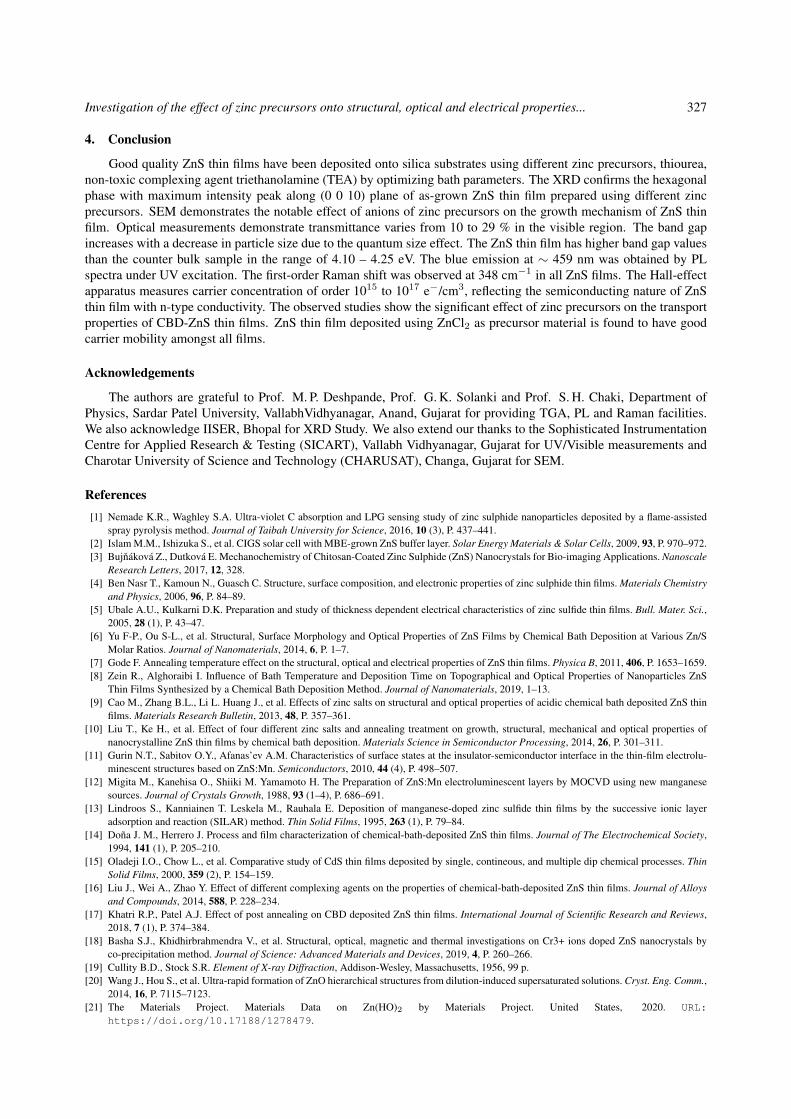
The Hall effect measurements were recorded by keeping probe current constant and varying magnetic field andmeasuring corresponding Hall voltage. The sketch for Hall voltage versus magnetic field is outlined in Fig. 13.The calculated values for the Hall coefficient, carrier concentration and mobility are listed in Table 4. The n-typeconductivity was observed in all ZnS films irrespective of zinc precursors used. The tabulated values show thatZnS–SO thin film has a high charge density and low conductivity compared to other thin films. The explanationof the observed results is that native defect states are generated during the growth of film act as scattering centers
326 Rajeshkumar P Khatri, Amitkumar J Patel
TABLE 4. Electrical parameter for as-grown ZnS thin films deposited using different zinc precur-sors: ZnS–Cl (a); ZnS–Ac (b); ZnS–SO (c)
Thin filmActivation energy
(eV) Resistivityρ (Ω·cm)
Conductivityσ (Ω−1·cm−1)
HallCoefficient
RH (cm3/C)
Carrierconcentrationη (cm−3)
Mobilityµ (cm2/Vs)
Ea1 Ea1
ZnS–Cl 0.75 — 2.08× 10⁴ 4.81× 10⁻⁵ 3.48× 10³ 1.79× 10¹⁵ 1.68× 10⁻¹
ZnS–Ac 0.81 — 1.63× 10⁴ 6.14 × 10⁻⁵ 1.71× 10² 3.65× 10¹⁶ 1.05× 10⁻²
ZnS–SO 0.59 2.55 8.52× 10⁴ 1.17× 10⁻⁵ 2.53 × 101 2.47 × 10¹⁷ 2.97× 10⁻⁴
for conduction electrons in the film.So defect chemistry and hence anions associated with zinc precursors play animportant role in the electrical transport properties of ZnS thin films. Fig. 14 represents the comparative graph forcarrier concentration, conductivity and mobility for ZnS thin films. It reveals from the graph that ZnS-Cl shows aconsiderable amount of conductivity compared to other samples even though its low carrier concentration. This is dueto the high mobility offered by it.
FIG. 13. Plot of Hall voltage VH versus magnetic field B for constant probe current of ZnS thinfilms deposited using different zinc precursors
FIG. 14. Comparative graph for carrier concentration, mobility and conductivity for as-grown ZnSthin films deposited using different zinc precursors
Investigation of the effect of zinc precursors onto structural, optical and electrical properties... 327
4. Conclusion
Good quality ZnS thin films have been deposited onto silica substrates using different zinc precursors, thiourea,non-toxic complexing agent triethanolamine (TEA) by optimizing bath parameters. The XRD confirms the hexagonalphase with maximum intensity peak along (0 0 10) plane of as-grown ZnS thin film prepared using different zincprecursors. SEM demonstrates the notable effect of anions of zinc precursors on the growth mechanism of ZnS thinfilm. Optical measurements demonstrate transmittance varies from 10 to 29 % in the visible region. The band gapincreases with a decrease in particle size due to the quantum size effect. The ZnS thin film has higher band gap valuesthan the counter bulk sample in the range of 4.10 – 4.25 eV. The blue emission at ∼ 459 nm was obtained by PLspectra under UV excitation. The first-order Raman shift was observed at 348 cm−1 in all ZnS films. The Hall-effectapparatus measures carrier concentration of order 1015 to 1017 e−/cm3, reflecting the semiconducting nature of ZnSthin film with n-type conductivity. The observed studies show the significant effect of zinc precursors on the transportproperties of CBD-ZnS thin films. ZnS thin film deposited using ZnCl2 as precursor material is found to have goodcarrier mobility amongst all films.
Acknowledgements
The authors are grateful to Prof. M. P. Deshpande, Prof. G. K. Solanki and Prof. S. H. Chaki, Department ofPhysics, Sardar Patel University, VallabhVidhyanagar, Anand, Gujarat for providing TGA, PL and Raman facilities.We also acknowledge IISER, Bhopal for XRD Study. We also extend our thanks to the Sophisticated InstrumentationCentre for Applied Research & Testing (SICART), Vallabh Vidhyanagar, Gujarat for UV/Visible measurements andCharotar University of Science and Technology (CHARUSAT), Changa, Gujarat for SEM.
References[1] Nemade K.R., Waghley S.A. Ultra-violet C absorption and LPG sensing study of zinc sulphide nanoparticles deposited by a flame-assisted
spray pyrolysis method. Journal of Taibah University for Science, 2016, 10 (3), P. 437–441.[2] Islam M.M., Ishizuka S., et al. CIGS solar cell with MBE-grown ZnS buffer layer. Solar Energy Materials & Solar Cells, 2009, 93, P. 970–972.[3] Bujnakova Z., Dutkova E. Mechanochemistry of Chitosan-Coated Zinc Sulphide (ZnS) Nanocrystals for Bio-imaging Applications. Nanoscale
Research Letters, 2017, 12, 328.[4] Ben Nasr T., Kamoun N., Guasch C. Structure, surface composition, and electronic properties of zinc sulphide thin films. Materials Chemistry
and Physics, 2006, 96, P. 84–89.[5] Ubale A.U., Kulkarni D.K. Preparation and study of thickness dependent electrical characteristics of zinc sulfide thin films. Bull. Mater. Sci.,
2005, 28 (1), P. 43–47.[6] Yu F-P., Ou S-L., et al. Structural, Surface Morphology and Optical Properties of ZnS Films by Chemical Bath Deposition at Various Zn/S
Molar Ratios. Journal of Nanomaterials, 2014, 6, P. 1–7.[7] Gode F. Annealing temperature effect on the structural, optical and electrical properties of ZnS thin films. Physica B, 2011, 406, P. 1653–1659.[8] Zein R., Alghoraibi I. Influence of Bath Temperature and Deposition Time on Topographical and Optical Properties of Nanoparticles ZnS
Thin Films Synthesized by a Chemical Bath Deposition Method. Journal of Nanomaterials, 2019, 1–13.[9] Cao M., Zhang B.L., Li L. Huang J., et al. Effects of zinc salts on structural and optical properties of acidic chemical bath deposited ZnS thin
films. Materials Research Bulletin, 2013, 48, P. 357–361.[10] Liu T., Ke H., et al. Effect of four different zinc salts and annealing treatment on growth, structural, mechanical and optical properties of
nanocrystalline ZnS thin films by chemical bath deposition. Materials Science in Semiconductor Processing, 2014, 26, P. 301–311.[11] Gurin N.T., Sabitov O.Y., Afanas’ev A.M. Characteristics of surface states at the insulator-semiconductor interface in the thin-film electrolu-
minescent structures based on ZnS:Mn. Semiconductors, 2010, 44 (4), P. 498–507.[12] Migita M., Kanehisa O., Shiiki M. Yamamoto H. The Preparation of ZnS:Mn electroluminescent layers by MOCVD using new manganese
sources. Journal of Crystals Growth, 1988, 93 (1–4), P. 686–691.[13] Lindroos S., Kanniainen T. Leskela M., Rauhala E. Deposition of manganese-doped zinc sulfide thin films by the successive ionic layer
adsorption and reaction (SILAR) method. Thin Solid Films, 1995, 263 (1), P. 79–84.[14] Dona J. M., Herrero J. Process and film characterization of chemical-bath-deposited ZnS thin films. Journal of The Electrochemical Society,
1994, 141 (1), P. 205–210.[15] Oladeji I.O., Chow L., et al. Comparative study of CdS thin films deposited by single, contineous, and multiple dip chemical processes. Thin
Solid Films, 2000, 359 (2), P. 154–159.[16] Liu J., Wei A., Zhao Y. Effect of different complexing agents on the properties of chemical-bath-deposited ZnS thin films. Journal of Alloys
and Compounds, 2014, 588, P. 228–234.[17] Khatri R.P., Patel A.J. Effect of post annealing on CBD deposited ZnS thin films. International Journal of Scientific Research and Reviews,
2018, 7 (1), P. 374–384.[18] Basha S.J., Khidhirbrahmendra V., et al. Structural, optical, magnetic and thermal investigations on Cr3+ ions doped ZnS nanocrystals by
co-precipitation method. Journal of Science: Advanced Materials and Devices, 2019, 4, P. 260–266.[19] Cullity B.D., Stock S.R. Element of X-ray Diffraction, Addison-Wesley, Massachusetts, 1956, 99 p.[20] Wang J., Hou S., et al. Ultra-rapid formation of ZnO hierarchical structures from dilution-induced supersaturated solutions. Cryst. Eng. Comm.,
2014, 16, P. 7115–7123.[21] The Materials Project. Materials Data on Zn(HO)2 by Materials Project. United States, 2020. URL:
https://doi.org/10.17188/1278479.

328 Rajeshkumar P Khatri, Amitkumar J Patel
[22] Echendu O.K., Weerasinghe A.R., et al. Characterization of n-type and p-type ZnS thin layers grown by an electrochemical method. Journalof Electronic Materials, 2013, 42 (4), P. 692–700.
[23] Moholkar A.V., Agawane G.L., et al. Influence of deposition temperature on morphological, optical, electrical and opto-electrical propertiesof highly textured nano-crystalline spray deposited CdO:Ga thin films. Applied Surface Science, 2010, 257 (1), P. 93–101.
[24] Ruffner J.A., Himel M.D., et al. Effects of low substrate temperature and ion assisted deposition on composition, optical properties, and stressof ZnS thin films. Applied Optics, 1989, 28 (24), 5209.
[25] Ahn H., Um Y. Post-annealing effects on ZnS thin films grown by using CBD method. Journal of Korean Physical Society, 2015, 67 (6),P. 1045–1050.
[26] Nadeem M.Y., Ahmed W. Optical properties of ZnS thin films. Turk. J. Phy., 2000, 24, P. 651–659.[27] Mendil R., Ben Ayadi Z., Ben Belgacem J., Djessas K. The properties of ZnS thin films prepared by rf-magnetron sputtering from nanoparticles
synthesized by solvothermal/hydrothermal route. J. Mater. Sci.: Mater. Electron., 2016, 27, P. 444–451.[28] Babu P., Reddy M., et al. Chemical bath deposition of Mn-doped ZnS thin films using greener complexing agents: Effect of Mn-doping on the
optical properties. Optik, 2017, 130, P. 608–618.[29] Fairbrother A., Izquierdo-Roca V., et al. ZnS grain size effects on near-resonant Raman scattering: optical non-destructive grain size estimation.
Cryst. Eng. Comm., 2014, 16, P. 4120–4125.[30] Vishwakarma R. Effect of substrate temperature on ZnS films prepared by thermal evaporation technique. J. Theor. Appl. Phys., 2015, 9,
P. 185–192.[31] Shukla V., Patel A. Effect of doping concentration on optical and electrical properties of intrinsic n-type ZnO (i-ZnO) and (Cu,Na and K) doped
p-type ZnO thin films grown by chemical bath deposition method. Nanosystems: physıcs, chemıstry, mathematıcs, 2020, 11 (4), P. 391–400.[32] Gode F., Gumus C. Influences of copper and manganese concentrations on the properties of polycrystalline ZnS:Cu and ZnS:Mn thin films.
Journal of Optoelectronics and Advanced Materials, 2009, 11 (4), P. 429–436.


![Available online at ScienceDirect...Aluminum Zinc Oxide (AZO) as alternative TCO reaches the most interest, because the precursors are nontoxic, cheap and earth-abundant [1,2,3]. There](https://img.pdfslide.net/doc/110x75/60bd1ad5fa2c58175963f017/available-online-at-sciencedirect-aluminum-zinc-oxide-azo-as-alternative-tco.jpg)