Embed Size (px)
Citation preview

Investigation of the impact of insulator material on the performance of dissimilarelectrode metal-insulator-metal diodesNasir Alimardani, Sean W. King, Benjamin L. French, Cheng Tan, Benjamin P. Lampert, and John F. Conley Jr.
Citation: Journal of Applied Physics 116, 024508 (2014); doi: 10.1063/1.4889798 View online: http://dx.doi.org/10.1063/1.4889798 View Table of Contents: http://scitation.aip.org/content/aip/journal/jap/116/2?ver=pdfcov Published by the AIP Publishing Articles you may be interested in Conduction processes in metal–insulator–metal diodes with Ta2O5 and Nb2O5 insulators deposited by atomiclayer deposition J. Vac. Sci. Technol. A 32, 01A122 (2014); 10.1116/1.4843555 Impact of top electrode on electrical stress reliability of metal-insulator-metal capacitor with amorphous ZrTiO 4film Appl. Phys. Lett. 96, 133501 (2010); 10.1063/1.3377914 Influence of the electrode material on Hf O 2 metal-insulator-metal capacitors J. Vac. Sci. Technol. B 27, 286 (2009); 10.1116/1.3071843 High-temperature conduction behaviors of HfO 2 / TaN -based metal-insulator-metal capacitors J. Appl. Phys. 102, 073706 (2007); 10.1063/1.2786712 Thin film solid-state reactions forming carbides as contact materials for carbon-containing semiconductors J. Appl. Phys. 101, 053714 (2007); 10.1063/1.2561173
[This article is copyrighted as indicated in the article. Reuse of AIP content is subject to the terms at: http://scitation.aip.org/termsconditions. Downloaded to ] IP:
128.193.38.25 On: Mon, 14 Jul 2014 16:34:45
Investigation of the impact of insulator material on the performanceof dissimilar electrode metal-insulator-metal diodes
Nasir Alimardani,1 Sean W. King,2 Benjamin L. French,3 Cheng Tan,1 Benjamin P. Lampert,1
and John F. Conley, Jr.1,a)
1School of Electrical Engineering and Computer Science, Oregon State University, Corvallis, Oregon 97331,USA2Logic Technology Development, Intel Corporation, Hillsboro, Oregon 97124, USA3Ocotillo Materials Laboratory, Intel Corporation, Chandler, Arizona 85248, USA
(Received 18 April 2014; accepted 2 June 2014; published online 14 July 2014)
The performance of thin film metal-insulator-metal (MIM) diodes is investigated for a variety of
large and small electron affinity insulators using ultrasmooth amorphous metal as the bottom
electrode. Nb2O5, Ta2O5, ZrO2, HfO2, Al2O3, and SiO2 amorphous insulators are deposited via
atomic layer deposition (ALD). Reflection electron energy loss spectroscopy (REELS) is utilized to
measure the band-gap energy (EG) and energy position of intrinsic sub-gap defect states for each in-
sulator. EG of as-deposited ALD insulators are found to be Nb2O5¼ 3.8 eV, Ta2O5¼ 4.4 eV,
ZrO2¼ 5.4 eV, HfO2¼ 5.6 eV, Al2O3¼ 6.4 eV, and SiO2¼ 8.8 eV with uncertainty of 60.2 eV.
Current vs. voltage asymmetry, non-linearity, turn-on voltage, and dominant conduction mechanisms
are compared. Al2O3 and SiO2 are found to operate based on Fowler-Nordheim tunneling. Al2O3
shows the highest asymmetry. ZrO2, Nb2O5, and Ta2O5 based diodes are found to be dominated by
Frenkel-Poole emission at large biases and exhibit lower asymmetry. The electrically estimated trap
energy levels for defects that dominate Frenkel-Poole conduction are found to be consistent with the
energy levels of surface oxygen vacancy defects observed in REELS measurements. For HfO2, con-
duction is found to be a mix of trap assisted tunneling and Frenkel-Poole emission. Insulator selec-
tion criteria in regards to MIM diodes applications are discussed. VC 2014 AIP Publishing LLC.
[http://dx.doi.org/10.1063/1.4889798]
I. INTRODUCTION
Thin film metal-insulator-metal (MIM) tunnel devices
have experienced a renewal in interest for ultra-high-speed
applications such as hot electron transistors,1,2 diodes for op-
tical rectenna based infrared (IR) energy harvesting,3,4 and
IR detectors,5,6 as well as for selector diodes for resistive
random access memory (RRAM),7,8 and MIM tunnel emis-
sion cathodes.9,10 Because of their simple structure and low
temperature processing, MIM building blocks are also being
considered for large area macroelectronics such as liquid
crystal display (LCD) backplanes.11,12 For many of these
applications, figures of merit include high asymmetry, strong
nonlinearity, and fast responsivity of current vs. voltage
(I-V) behavior at low voltages.
The standard approach to achieving high speed rectifica-
tion in an MIM device is based on Fowler-Nordheim tunnel-
ing (FNT) conduction in conjunction with the use of
dissimilar work function metal electrodes (where UM1 6¼UM2)
to produce an asymmetric, polarity dependent electron tunnel-
ing barrier.13 FNT conduction is exponentially dependent
upon the metal/insulator barrier height, electric field, and in-
sulator thickness. The uniformity of the electric field is criti-
cal. Attention must therefore be paid to metal/insulator
interface roughness as well as insulator quality.
Although many investigations of MIM tunnel diodes
have been reported over the years, the majority of these stud-
ies were adversely affected by two technological limitations.
The first limitation of previous studies is that they made use
of inherently rough polycrystalline metal bottom electrodes.
The as-deposited roughness of poly-crystalline metal films
can be several times larger than the tunnel barrier thickness. It
has been theoretically predicted that interfacial roughness can
influence the tunneling current across junctions14 and we
experimentally demonstrated that roughness of the bottom
metal electrode can overwhelm the influence of work function
difference (DUM) on MIM current-voltage (I-V) characteris-
tics as well as deteriorate device yield.15–17 The second limi-
tation of most previous experimental investigations of MIM
diodes is that they focused on the use of insulators produced
by oxidation or nitridation of these underlying polycrystalline
metal electrodes.5,6,10,18–20 Insulators formed in this manner
are typically of low quality which can have a severe negative
impact on device performance and repeatability.
Thus, although it appears that much work has been
reported on thin film MIM diodes, these studies have involved
primarily low quality oxides or nitrides of the polycrystalline
bottom metal electrode and have resulted in poor characteris-
tics or repeatibilty.18–20 In addition, the practice of using
native oxides and nitrides strictly limits the range of metal-
insulator combinations that can be studied. To target different
applications, it is desirable to pair up insulators having a range
of band-gaps and electron affinities with small and large work
a)Author to whom correspondence should be addressed. Electronic mail:
0021-8979/2014/116(2)/024508/11/$30.00 VC 2014 AIP Publishing LLC116, 024508-1
JOURNAL OF APPLIED PHYSICS 116, 024508 (2014)
[This article is copyrighted as indicated in the article. Reuse of AIP content is subject to the terms at: http://scitation.aip.org/termsconditions. Downloaded to ] IP:
128.193.38.25 On: Mon, 14 Jul 2014 16:34:45

function metals. For example, insulators with large electron
affinities (low barrier heights), such as Nb2O5 and Ta2O5, are
potential candidates for rectenna based IR energy harvesting
applications which must operate in a very low bias regime.4,20
On the other hand, Al2O3 and SiO2 with relatively large band-
gaps and small electron affinity values are desired candidates
for liquid crystal display backplanes and their use is already
well established in the display industry. HfO2 and ZrO2 have
intermediate band-gaps and electron affinities and HfO2 is
now used in gate dielectrics in complementary metal-oxide-
semiconductor (CMOS) transistors. HfO2 and Ta2O5 are both
promising RRAM materials.21,22 Despite the importance of
the insulator in determining MIM performance, a systematic
study of the impact on thin film diode performance of various
insulators using a fixed electrode pair has not been conducted.
We have shown previously that using atomic layer depo-
sition (ALD) of Al2O3 on atomically smooth (0.3 nm RMS
with 3 nm peak roughness) bottom metal electrodes large
area high quality MIM diodes with well controlled FNT can
be realized.16,17 ALD is based on self-saturating reactions,
allowing for high conformality, precise thickness control, and
uniformity over large surface areas. An additional benefit of
ALD is that it allows deposition of a wide range of high qual-
ity insulators independent of the bottom electrode material.23
In this work, MIM devices fabricated on ultra-smooth
ZrCuAlNi (ZCAN) amorphous metal bottom electrodes
using Nb2O5, Ta2O5, ZrO2, HfO2, Al2O3, and SiO2 amor-
phous insulators deposited via ALD are investigated. MIM
diode performance, including current vs. voltage asymmetry,
non-linearity, and dominant conduction mechanism is com-
pared as a function of temperature. Reflection electron
energy loss spectroscopy (REELS) is utilized to measure the
band-gap energy and energy position of sub-gap defect states
for each of these insulators. The REELS measured band-
gaps are used in the analysis of conduction mechanisms and
the energy position of sub-band gap defect states are com-
pared with electrical estimates of trap energy levels. Finally,
insulator selection criteria are discussed with regard to
potential applications.
II. EXPERIMENTAL
Si coupons coated with a 100 nm thick film of thermally
grown SiO2 were used as starting substrates for MIM device
fabrication. ZCAN amorphous metal was selected as the bot-
tom electrode (M1) due to its atomically smooth as-deposited
surface (RMS roughness� 0.3 nm).16,24 Using an ultra-
smooth bottom electrode ensures that conduction is not
dominated by "hot spots" due to field enhancement at surface
topography.15 ZCAN was deposited via DC magnetron sput-
tering using a Zr40Cu35Al15Ni10 metal target with no inten-
tional substrate heating. Thin insulator tunnel barriers, with
the exception of SiO2, were deposited via ALD in a Picosun
SUNALE R-150B chamber at a temperature of 250 �C using
deionized water as the oxidant. Metal precursors used were
niobium ethoxide for Nb2O5, tantalum ethoxide for Ta2O5,
tetrakis (ethylmethylamino) zirconium (TEMAZr) for ZrO2,
tetrakis (ethylmethylamino) hafnium (TEMAHf) for HfO2,
and trimethylaluminum (TMA) for Al2O3. The SiO2 films
were deposited in a Cambridge NanoTech Fiji plasma
enhanced atomic layer deposition (PEALD) tool using tris
(dimethylamino) silane ([(CH3)2N]3SiH) and an O2 remote
plasma at a substrate temperature of 250 �C. Insulator thick-
nesses of 10 nm were chosen to suppress direct tunneling so
as to more easily distinguish FNT conduction. Aluminum
dots (�0.2 mm2), thermally evaporated through a shadow
mask, were used as the top electrode (M2).
The thicknesses of insulator films deposited on Si were
measured with a J.A. Woollam WVASE32 spectroscopic el-
lipsometer using a Cauchy model. Spectroscopic ellipsome-
try was also used to measure the index of refraction, n, in the
wavelength range of 400–1200 nm in order to estimate the
optical dielectric constant (n2).
Using electron beam and X-ray diffraction (XRD), it
was determined that all ALD films were amorphous as-
deposited. Crystalline phases in insulator films may create
conduction paths for electrons and thus facilitate defect-
dominated leakage mechanisms.25 Likewise, crystallization
of bottom electrode increases electrode surface roughness
which can generate local electric field enhancements or hot
spots.26 Atomic force microscopy (AFM) shows an increase
in surface roughness and XRD shows signs of crystallization
when ZCAN is annealed at 380 �C and above. In order to
avoid the possibility of crystallization of either the ALD
insulators or the ZCAN bottom electrodes, all devices are
studied as-deposited, without annealing treatments.
A Kelvin probe electrostatic voltmeter was used to deter-
mine metal electrode work functions. The work function of
the ZCAN electrode (UZCAN) was found to be approximately
4.8 eV and the difference between the ZCAN and Al work
functions (DU¼UZCAN�UAl) was approximately 0.6 eV.
These values were confirmed by the extrapolation of Fowler-
Nordheim plots, reported in detail elsewhere.27
Dielectric constants were determined using capacitive
vs. voltage (C-V) measurements taken on an Agilent B1500
semiconductor device parameter analyzer. Room tempera-
ture I-V measurements were performed on a probe station in
a dark box using an Agilent 4156C semiconductor parameter
analyzer; the noise floor of this system is estimated to be on
the order of 100 pA. All I-V measurements at temperatures
ranging from 25 to 100 �C were conducted using a
Temptronic gold plated ThermoChuck and a probe station in
a dark box. I-V measurements below the room temperature
were performed in a LakeShore EMPX-HF cryogenic probe
station. I-V measurements were performed with the ZCAN
bottom electrode (M1) held at ground and with bias applied
to the Al top gate (M2). To mitigate the impact of displace-
ment current, all I-V curves were swept from zero bias to ei-
ther the maximum positive or negative bias. We define the
turn-on bias (VON) as the bias at which current begins to
increase exponentially with voltage. Two key figures of
merit are defined to characterize the devices. I-V asymmetry,
gasym., is defined as negative current divided by positive cur-
rent jI�/Iþj, so that gasym¼ 1 indicates symmetric operation.
Non-linearity, fNL, is defined as (dI/dV)/(I/V).
A VG 350 Auger electron spectroscopy system was used
for REELS analysis to estimate band-gaps and defect levels.
The details of the system and REELS experiments have been
024508-2 Alimardani et al. J. Appl. Phys. 116, 024508 (2014)
[This article is copyrighted as indicated in the article. Reuse of AIP content is subject to the terms at: http://scitation.aip.org/termsconditions. Downloaded to ] IP:
128.193.38.25 On: Mon, 14 Jul 2014 16:34:45

reported elsewhere.28,29 Briefly, the oxide dielectrics were
transferred ex-situ to the REELS system and spectra were col-
lected using 0.5 and 2.5 keV primary electron beam energies.
The hemispherical electron energy analyzer was operated at a
resolution of 0.2 eV with a pass energy of 8 eV. A shallow
surface exit angle of 80� relative to the surface normal was
used to improve surface sensitivity and reduce the background
intensity from inelastically scattered electrons in the low-
energy tail of the primary elastic peak. The band-gaps of the
oxide dielectrics were estimated from the raw REELS spectra
by linearly extrapolating the leading edge of the electron
energy loss spectrum to the elastic peak baseline. A 3-keV
Arþ ion sputtering beam operated at 10 lA/cm2 was addition-
ally utilized to remove surface contamination from ex-situtransfer and induce surface defects. Features detected in the
REELS spectra below the band-gap energy were treated as ei-
ther extended states arising from the amorphous structure of
the oxide dielectrics or more specific defect states.
Band diagrams were simulated using the Boise State
University Band Diagram program.30 Materials parameters
used in simulations are based on Kelvin probe and REELS
measurements as well as literature values reported for ALD
insulators deposited using the same precursors and process
temperatures.
III. RESULTS AND DISCUSSION
A. REELS investigations
Shown in Fig. 1 are REELS spectra taken from both as-
deposited and Arþ sputtered 10 nm thick ALD films of (a)
SiO2, (b) Al2O3, (c) HfO2, (d) ZrO2, (e) Ta2O5, and (f)
Nb2O5, each on 150 nm thick ZCAN metal films on Si. As
illustrated in each figure, the band-gaps were estimated via
linear extrapolation of the leading edge of the loss for each
ALD film. Defect levels were determined from the loss peaks
that appeared after Arþ sputtering.28,29
As has been previously reported for PECVD and ther-
mal SiO2,29,31 a large surface band-gap of 8.8 6 0.2 eV was
observed for the as-deposited PEALD SiO2 film and Arþ
sputter induced surface oxygen vacancy (SOV) defect cen-
ters were observed to appear in the band-gap at �5.0 and
7.2 eV. Smaller band-gaps of 5.4–6.6 eV were observed for
as-deposited Al2O3, HfO2, and ZrO2, where Arþ sputtering
was also observed to induce surface oxygen vacancy related
defect centers in the band-gap.31 For Al2O3, the surface
band-gap of 6.4 6 0.2 eV is substantially reduced relative to
the value of 7.8 eV typically quoted for sapphire and has
been previously attributed to the presence of residual hydro-
gen, organics, and a slight non-stoichiometry in the ALD de-
posited film.31 Similar to SiO2, Arþ sputtering of Al2O3
induces surface oxygen vacancy defect centers just below the
conduction band minimum centered at approximately 5.0 eV.
HfO2 and ZrO2 exhibit similar band-gaps of 5.6 6 0.2
and 5.4 6 0.2 eV, respectively. The Arþ sputter induced
defects states for HfO2 and ZrO2 were also similar and
exhibited a broader distribution deeper in the band-gap (cen-
tered at approximately 2–2.5 eV above the elastic peak and
extending up to the conduction band edge). These Arþ sput-
ter induced defect centers have been previously observed in
photoemission experiments by Morant32 for ZrO2 and are
consistent with the oxygen vacancy defect centers modeled
by Robertson33 and Foster34,35 for both ZrO2 and HfO2. In
contrast, electrical and spectroscopic ellipsometry measure-
ments have observed the presence of shallower trap and
defect states distributed at 0.3–1.2 eV below the HfO2 con-
duction band minimum.36–39 However, this is still consistent
with the REELS measurements where the distribution of Arþ
sputter induced defects (centered at 3.4 eV below the con-
duction band) extends up to the conduction band minimum.
FIG. 1. REELS spectra of as-deposited and Arþ sputtered thin films of (a) SiO2, (b) Al2O3, (c) HfO2, (d) ZrO2, (e) Ta2O5, and (f) Nb2O5. The intersection of
the gray dashed lines indicates the onset of the loss spectrum for the purpose of calculating the band-gap energy. Peaks in the post Arþ sputtered films indicate
distinct defect levels.
024508-3 Alimardani et al. J. Appl. Phys. 116, 024508 (2014)
[This article is copyrighted as indicated in the article. Reuse of AIP content is subject to the terms at: http://scitation.aip.org/termsconditions. Downloaded to ] IP:
128.193.38.25 On: Mon, 14 Jul 2014 16:34:45
In this regard, it is important to note that the Arþ sputter
induced sub-gap defect states detected in REELS are primar-
ily located within a few atomic layers of the surface and
likely exhibit a different range of valence states relative to
the distribution of related bulk traps/defects in the ALD ox-
ide dielectric. Therefore, it is plausible that the REELS
defects in the upper part of the Arþ sputter induced defect
tail are more directly related to the electrically and optically
detected trap / defect states.
Analysis of the REELS spectra from as-deposited Ta2O5
and Nb2O5 indicated substantially smaller band-gaps of
4.4 6 0.2 and 3.8 6 0.2 eV, respectively. Similar to the other
oxide dielectrics investigated, Arþ sputtering was also
observed to create defect states in the band-gap of Ta2O5 and
Nb2O5 that based on analogy are also believed to be surface
oxygen vacancies. However, the defect states for Ta2O5 and
Nb2O5 do not show a clear maximum in peak intensity. They
are instead manifested as a broad tail below the elastic peak
that merges with the turn-on in electron energy loss due to
exciton creation and promotion of valence band electrons
into the conduction band. To more clearly see the position of
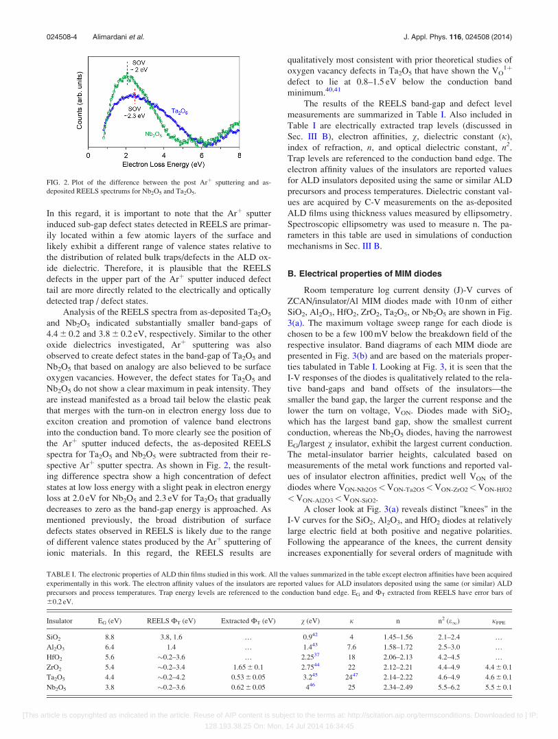
the Arþ sputter induced defects, the as-deposited REELS
spectra for Ta2O5 and Nb2O5 were subtracted from their re-
spective Arþ sputter spectra. As shown in Fig. 2, the result-
ing difference spectra show a high concentration of defect
states at low loss energy with a slight peak in electron energy
loss at 2.0 eV for Nb2O5 and 2.3 eV for Ta2O5 that gradually
decreases to zero as the band-gap energy is approached. As
mentioned previously, the broad distribution of surface
defects states observed in REELS is likely due to the range
of different valence states produced by the Arþ sputtering of
ionic materials. In this regard, the REELS results are
qualitatively most consistent with prior theoretical studies of
oxygen vacancy defects in Ta2O5 that have shown the VO1þ
defect to lie at 0.8–1.5 eV below the conduction band
minimum.40,41
The results of the REELS band-gap and defect level
measurements are summarized in Table I. Also included in
Table I are electrically extracted trap levels (discussed in
Sec. III B), electron affinities, v, dielectric constant (j),
index of refraction, n, and optical dielectric constant, n2.
Trap levels are referenced to the conduction band edge. The
electron affinity values of the insulators are reported values
for ALD insulators deposited using the same or similar ALD
precursors and process temperatures. Dielectric constant val-
ues are acquired by C-V measurements on the as-deposited
ALD films using thickness values measured by ellipsometry.
Spectroscopic ellipsometry was used to measure n. The pa-
rameters in this table are used in simulations of conduction
mechanisms in Sec. III B.
B. Electrical properties of MIM diodes
Room temperature log current density (J)-V curves of
ZCAN/insulator/Al MIM diodes made with 10 nm of either
SiO2, Al2O3, HfO2, ZrO2, Ta2O5, or Nb2O5 are shown in Fig.
3(a). The maximum voltage sweep range for each diode is
chosen to be a few 100 mV below the breakdown field of the
respective insulator. Band diagrams of each MIM diode are
presented in Fig. 3(b) and are based on the materials proper-
ties tabulated in Table I. Looking at Fig. 3, it is seen that the
I-V responses of the diodes is qualitatively related to the rela-
tive band-gaps and band offsets of the insulators—the
smaller the band gap, the larger the current response and the
lower the turn on voltage, VON. Diodes made with SiO2,
which has the largest band gap, show the smallest current
conduction, whereas the Nb2O5 diodes, having the narrowest
EG/largest v insulator, exhibit the largest current conduction.
The metal-insulator barrier heights, calculated based on
measurements of the metal work functions and reported val-
ues of insulator electron affinities, predict well VON of the
diodes where VON-Nb2O5<VON-Ta2O5<VON-ZrO2<VON-HfO2
<VON-Al2O3<VON-SiO2.
A closer look at Fig. 3(a) reveals distinct "knees" in the
I-V curves for the SiO2, Al2O3, and HfO2 diodes at relatively
large electric field at both positive and negative polarities.
Following the appearance of the knees, the current density
increases exponentially for several orders of magnitude with
FIG. 2. Plot of the difference between the post Arþ sputtering and as-
deposited REELS spectrums for Nb2O5 and Ta2O5.
TABLE I. The electronic properties of ALD thin films studied in this work. All the values summarized in the table except electron affinities have been acquired
experimentally in this work. The electron affinity values of the insulators are reported values for ALD insulators deposited using the same (or similar) ALD
precursors and process temperatures. Trap energy levels are referenced to the conduction band edge. EG and AT extracted from REELS have error bars of
60.2 eV.
Insulator EG (eV) REELS AT (eV) Extracted AT (eV) v (eV) j n n2 (e1) jFPE
SiO2 8.8 3.8, 1.6 … 0.942 4 1.45–1.56 2.1–2.4 …
Al2O3 6.4 1.4 … 1.443 7.6 1.58–1.72 2.5–3.0 …
HfO2 5.6 �0.2–3.6 … 2.2537 18 2.06–2.13 4.2–4.5 …
ZrO2 5.4 �0.2–3.4 1.65 6 0.1 2.7544 22 2.12–2.21 4.4–4.9 4.4 6 0.1
Ta2O5 4.4 �0.2–4.2 0.53 6 0.05 3.245 2447 2.14–2.22 4.6–4.9 4.6 6 0.1
Nb2O5 3.8 �0.2–3.6 0.62 6 0.05 446 25 2.34–2.49 5.5–6.2 5.5 6 0.1
024508-4 Alimardani et al. J. Appl. Phys. 116, 024508 (2014)
[This article is copyrighted as indicated in the article. Reuse of AIP content is subject to the terms at: http://scitation.aip.org/termsconditions. Downloaded to ] IP:
128.193.38.25 On: Mon, 14 Jul 2014 16:34:45

small increases in applied bias. The knees indicate a change
in the dominant conduction mechanism that, as discussed
below, is attributed to the onset of FN tunneling dominance.
The relative position of the knees corresponds roughly to the
relative barrier heights of the diodes, appearing at the lowest
voltage for the HfO2 diodes (smallest barrier) and at the larg-
est voltage for the SiO2 devices (largest barrier). The ZrO2,
Ta2O5, and Nb2O5 diodes, on the other hand, do not exhibit
knees in their I-V response. These diodes show large leakage
current at a very low bias range. The ZrO2, Ta2O5, and
Nb2O5 insulators all have large electron affinities and thus
form small energy barriers with the electrodes, which can
allow a thermally activated conduction mechanism such as
Schottky emission (SE) to be significant at room temperature.
Two key figures of merit for tunnel diodes are I-V asym-
metry (gasym) and non-linearity (fNL). It is often assumed that
MIM diodes operate based on FNT. Assuming that conduction
is dominated by FNT and neglecting non-idealities such as the
formation of metal oxide interfacial layers (ILs), or non-ideal
modifications to the effective work function due to the pres-
ence of the dielectric,48 the asymmetry polarity and maximum
asymmetry (gmax) of M1IM2 diodes should be determined pri-
marily by the built in field induced by the vacuum electrode
work function difference (DAM¼AM1�AM2). In the ideal
case, M1IM2 diodes with the same top and bottom metal elec-
trodes should exhibit qualitatively similar I-V asymmetry, in-
dependent of the tunnel insulator. The gasym and fNL data
however, plotted in Fig. 4, suggest that the assumption of
FNT dominated conduction is not valid for all insulators. The
diodes, in Fig. 4(a), show different asymmetric properties.
gmax is roughly in order of band-gap. While the Al2O3 diode
exhibits gmax of more than þ1500, the ZrO2, HfO2, and SiO2
diodes exhibit gmax two orders of magnitude lower with the
HfO2 diodes showing asymmetry of opposite polarity. Note
that while the band-gap of SiO2 is larger than Al2O3, the gmax
of the SiO2 diode is less than that of Al2O3 diode because of
two reasons. First, as it is seen in Fig. 3(a), the SiO2 diodes
show larger leakage at low voltages due to deep trap level at
3.8 eV below the conduction band minimum which provides a
path for trap assisted tunneling (TAT) at low voltages.
Second, as it is seen in Fig. 4(a), at around above 6 V FNT
begins to dominate and forward asymmetry increases but
before reaching to larger asymmetry values, insulator break-
down occurs. The Ta2O5 and Nb2O5 diodes are roughly
symmetric.
The abrupt changes in fNL with voltage (Fig. 3(b)) are
likely due either to changes in the dominant conduction
mechanism through the insulator or to charge trapping. The
onset voltage of rapidly increasing fNL is correlated roughly
with the insulator barrier heights with Ta2O5, Nb2O5, and
ZrO2 grouped together followed by HfO2, Al2O3, and finally
SiO2. Different maximum values of fNL (fNL-max) are
observed.
For diodes dominated by FNT, the bias at which fNL-max
occurs correlates with the onset of FNT and the magnitude
of fNL-max in these devices is an indication of the extent by
which FNT dominates these devices. Current due to FNT,
IFNT, may be described as
IFNT ¼ C1
1
/b
Vð Þ2 exp �C2m�12/
32
b
V
!; (1)
where C1 and C2 are universal constants independent of
materials properties, /b is the energy barrier height between
the Fermi-level of the injecting electrode and the conduction
band minimum of the insulator, m* is the effective electron
mass for tunneling electron, and V is voltage.13,49 To exam-
ine whether the dominant conduction process is related to
FNT, the room temperature MIM J-V data from Fig. 3(a)
were re-plotted as ln(I/V2) and (1/V) in Fig. 5. For each de-
vice, the bias range for fitting is chosen on the basis of the
diode current response. JFNT is exponentially dependent on
FIG. 3. (a) Plots of log (J) vs. V for M1IM2 diodes made on ZrCuAlNi bot-
tom electrodes with 10 nm of either SiO2, Al2O3, HfO2, ZrO2, Ta2O5, or
Nb2O5 and Al top electrodes. (b) Simulated band diagrams illustrating these
diodes in equilibrium.
FIG. 4. Plots of (a) log (gasym) and (b) fNL vs. voltage for M1IM2 diodes
made on ZrCuAlNi bottom electrodes with 10 nm of either SiO2, Al2O3,
HfO2, ZrO2, Ta2O5, or Nb2O5, and Al top electrodes.
024508-5 Alimardani et al. J. Appl. Phys. 116, 024508 (2014)
[This article is copyrighted as indicated in the article. Reuse of AIP content is subject to the terms at: http://scitation.aip.org/termsconditions. Downloaded to ] IP:
128.193.38.25 On: Mon, 14 Jul 2014 16:34:45

the applied voltage and requires high electric fields so that
electrons may tunnel into the conduction band of the insula-
tor. For the SiO2, Al2O3, and HfO2 devices, the voltage range
above the occurrence of the VON "knee" in the log(J)-V plots
from Fig. 3(a) were selected. As there is no knee in log(J)-V
plots of the ZrO2, Ta2O5, and Nb2O5 devices, the J-V curves
over the last four orders of magnitude increase in current
response were analyzed. A linear relationship between
ln(I/V2) and (1/V) is an indication that FNT is the dominant
conduction mechanism over the bias range. An R2 value
greater than 0.999 was taken to indicate an excellent fit. It is
seen in Fig. 5 that the SiO2, Al2O3, and HfO2 devices all ex-
hibit highly linear ln(I/V2) vs. (1/V) curves with R2> 0.999
for both positive and negative polarities. Thus, for the volt-
age range defined, FNT is tentatively assigned as the domi-
nant conduction mechanism for the SiO2, Al2O3, and HfO2
devices. Diodes made with ZrO2, Ta2O5, and Nb2O5, how-
ever, exhibit poor with R2 values ranging from 0.98 to 0.99,
indicating that FNT does not dominate conduction in these
devices.
Besides FNT and direct tunneling (which should be sup-
pressed in the 10 nm thick films), possible competing con-
duction mechanisms include SE, Frenkel-Poole emission
(FPE), and space-charge-limited (SCL) conduction. SCL is
ruled out because the current density (J) does not exhibit a
V2 dependence.50 SE conduction is limited by emission over
the energy barrier at the interface. For low energy barrier
devices under low bias, SE can be dominant. Current con-
duction due to Schottky emission, ISE, is described as
ISE ¼ A�T2 exp�q /b �
ffiffiffiffiffiffiffiffiffiffiffiffiffiffiffiffiffiffiffiffiffiffiqV=4pjre0
p� �kT
" #; (2)
where A* is the effective Richardson constant, T is tempera-
ture, q is the elementary charge, jr is the optical dielectric
constant, e0 is the permittivity of free space, and k is
Boltzmann’s constant.49 To assess the contribution of SE,
the high field J-V data from Fig. 3(a) were replotted as ln(I/
T2) vs. V1/2. A linear relationship between ln(I/T2) and V1/2
is an indication that SE is dominant. None of these plots (not
shown here) demonstrate good linear fits. Hence, SE is not
found to dominate conduction mechanism in the high field
regime. Note that we previously showed that SE dominates
both Ta2O5 and Nb2O5 in the low bias regime.51
For FPE, conduction is limited by emission from traps
in the bulk of the oxide, where
IFPE ¼ V exp�q /T �
ffiffiffiffiffiffiffiffiffiffiffiffiffiffiffiffiffiffiffiqV=pjre0
p� �kT
" #; (3)
where /T is the trap energy depth referenced to the insulator
conduction band minimum.49 To determine whether the
dominant conduction mechanism is related to FPE, the high
field J-V data from Fig. 3(a) replotted as ln (IFPE/V) vs. V1/2
in Fig. 6. It is seen that the 10 nm thick ZrO2, Ta2O5, and
Nb2O5 devices produce linear fits in the FPE plots with
R2> 0.999, suggesting that FPE is the dominate conduction
mechanism for these devices. For SiO2 and Al2O3, the linear-
ity was poor (R2< 0.98), consistent with our tentative assign-
ment of FNT dominated conduction for these devices. The
linearity of the HfO2 devices, on the other hand, was charac-
terized by R2¼ 0.997, suggesting that in addition to FNT,
thermal conduction mechanisms also play a role.
To assess the validity of the tentative FPE assignment
for Nb2O5, Ta2O5, and ZrO2, the dynamic relative dielectric
constants, jr, are extracted from the slopes of the plots in
Fig. 6. For Ta2O5, Nb2O5, and ZrO2, the extracted values of
jr are 4.6 6 0.1, 5.5 6 0.1, and 4.4 6 0.1, respectively. Note
that the values of jr are essentially the same for both polar-
ities. Although it is clear that all of these extracted dielectric
constants are much smaller than the static dielectric constant
j measured via C-V and shown in Table I, it is the optical
dielectric constant to which they should be compared.52–54
The optical dielectric constant for each material was esti-
mated from the refractive index, n, which was measured in
the wavelength range of 400–1200 nm using spectroscopic
ellipsometry. As summarized in Table I, n2 was measured to
range from 5.5 to 6.2 for Nb2O5, from 4.6 to 4.95 for Ta2O5,
and from 4.5 to 4.9 for ZrO2. The jr values extracted from
the FPE plots (5.5 6 0.1 for Nb2O5, 4.6 6 0.1 for Ta2O5, and
4.4 6 0.1 for ZrO2), are all at the low end of the range of val-
ues measured optically, supporting the assignment of FPE as
the dominant mechanism at high fields in these films.
FIG. 5. I-V curves from Fig. 3(a) fitted to FNT plots of ln (I/V2) vs. 1/V.
Green and blue curves represent negative and positive polarities, respec-
tively. Curves showing R2� 0.999 are considered to be highly linear and
exhibiting FNT as the dominant conduction mechanism.
024508-6 Alimardani et al. J. Appl. Phys. 116, 024508 (2014)
[This article is copyrighted as indicated in the article. Reuse of AIP content is subject to the terms at: http://scitation.aip.org/termsconditions. Downloaded to ] IP:
128.193.38.25 On: Mon, 14 Jul 2014 16:34:45
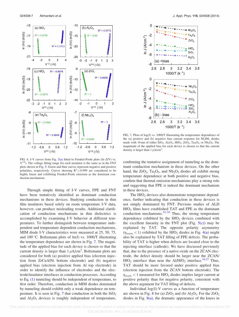
Through simple fitting of I-V curves, FPE and FNT
have been tentatively identified as dominant conduction
mechanisms in these devices. Studying conduction in thin
film insulators based solely on room temperature I-V data,
however, can produce misleading results. Additional clarifi-
cation of conduction mechanisms in thin dielectrics is
accomplished by examining I-V behavior at different tem-
peratures. To further distinguish between temperature inde-
pendent and temperature dependent conduction mechanisms,
MIM diode I-V characteristics were measured at 25, 50, 75,
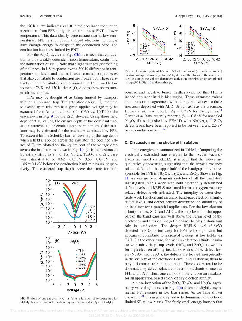
and 100 �C. Boltzmann plots of ln(J) vs. 1000/T illustrating
the temperature dependence are shown in Fig. 7. The magni-
tude of the applied bias for each device is chosen so that the
current density is larger than 1 lA/cm2. Boltzmann plots are
considered for both (a) positive applied bias (electron injec-
tion from ZrCuAlNi bottom electrode) and (b) negative
applied bias (electron injection from Al top electrode) in
order to identify the influence of electrodes and the elec-
trode/insulator interfaces in conduction processes. According
to Eq. (1) tunneling should be independent of temperature, to
first order. Therefore, conduction in MIM diodes dominated
by tunneling should exhibit only a weak dependence on tem-
perature. It is seen in Fig. 7 that conduction in both the SiO2
and Al2O3 devices is roughly independent of temperature,
confirming the tentative assignment of tunneling as the dom-
inant conduction mechanism in these devices. On the other
hand, the ZrO2, Ta2O5, and Nb2O5 diodes all exhibit strong
temperature dependence at both positive and negative bias,
confirm that thermal emission mechanisms play a strong role
and suggesting that FPE is indeed the dominant mechanism
in these devices.
The HfO2 devices also demonstrate temperature depend-
ence, further indicating that conduction in these devices is
not simply dominated by FNT. Previous studies of ALD
HfO2 films have established TAT and FPE as the dominant
conduction mechanisms.53–55 Thus, the strong temperature
dependence exhibited by the HfO2 devices combined with
the excellent linearity in the FNT plot (Fig. 5(c)) may be
explained by TAT. The opposite polarity asymmetry
(gasym.< 1) exhibited by the HfO2 diodes in Fig. 4(a) might
also be explained by TAT filling of FPE defects. The proba-
bility of TAT is higher when defects are located close to the
injecting interface (cathode). We have discussed previously
that, due to the presence of a native oxide on the ZCAN elec-
trode, the defect density should be larger near the ZCAN/
HfO2 interface than near the Al/HfO2 interface.16,27 Thus,
TAT should be more favored under positive applied bias
(electron injection from the ZCAN bottom electrode). The
gasym.< 1 measured for HfO2 diodes implies larger current at
positive polarity than for negative polarity, consistent with
the above argument for TAT filling of defects.
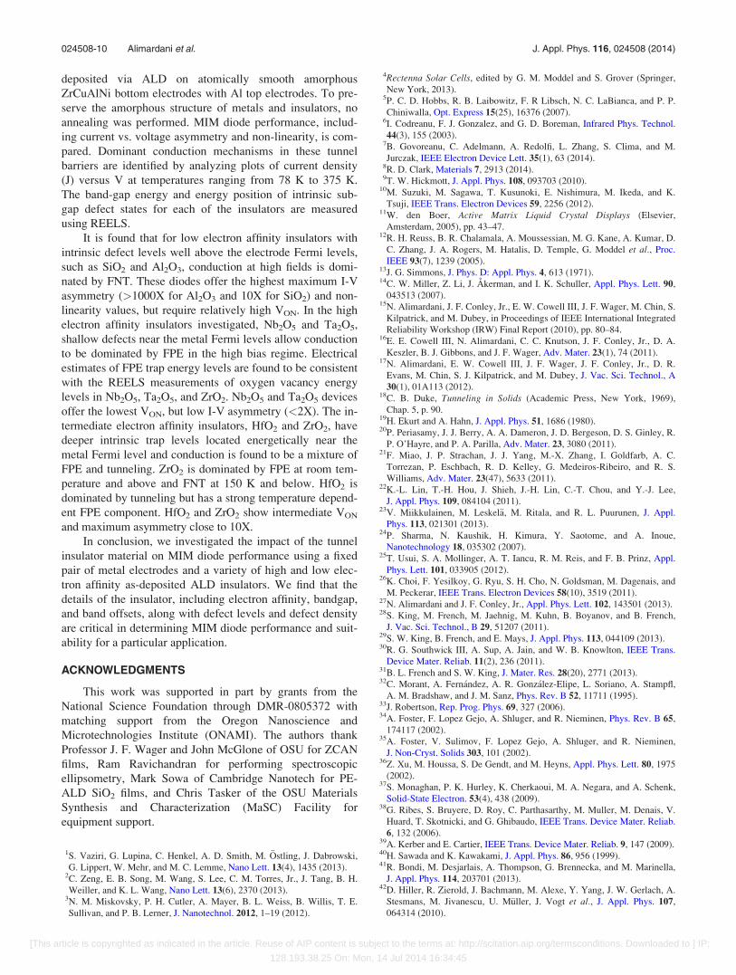
Individual log(J)-V curves as a function of temperature
are shown in Fig. 8 for (a) ZrO2 and (b) Al2O3. For the ZrO2
diodes in Fig. 8(a), the dramatic appearance of the knees in
FIG. 7. Plots of log(J) vs. 1000/T illustrating the temperature dependence of
the (a) positive and (b) negative bias current response for M1IM2 diodes
made with 10 nm of either SiO2, Al2O3, HfO2, ZrO2, Ta2O5, or Nb2O5. The
magnitude of the applied bias for each device is chosen so that the current
density is larger than 1 lA/cm2.
FIG. 6. I-V curves from Fig. 3(a) fitted to Frenkel-Poole plots (ln (I/V) vs.
V1/2). The voltage fitting range for each insulator is the same as in the FNT
plots shown in Fig. 5. Green and blue curves represent negative and positive
polarities, respectively. Curves showing R2� 0.999 are considered to be
highly linear and exhibiting Frenkel-Poole emission as the dominant con-
duction mechanism.
024508-7 Alimardani et al. J. Appl. Phys. 116, 024508 (2014)
[This article is copyrighted as indicated in the article. Reuse of AIP content is subject to the terms at: http://scitation.aip.org/termsconditions. Downloaded to ] IP:
128.193.38.25 On: Mon, 14 Jul 2014 16:34:45
the 150 K curve indicates a shift in the dominant conduction
mechanism from FPE at higher temperatures to FNT at lower
temperature. This data clearly demonstrate that at low tem-
peratures, FPE is shut down, trapped electrons no longer
have enough energy to escape to the conduction band, and
conduction becomes limited by FNT.
For the Al2O3 device in Fig. 8(b), it is seen that conduc-
tion is only weakly dependent upon temperature, confirming
the domination of FNT. Note that slight changes (sharpening
of the knees) in I-V response over a 300 K difference in tem-
perature as defect and thermal based conduction processes
that also contribute to conduction are frozen out. These rela-
tively minor contributions are eliminated at 150 K and below
so that at 78 K and 150 K, the Al2O3 diodes show sharp turn-
on characteristics.
FPE may be thought of as being limited by transport
through a dominant trap. The activation energy, Ea, required
to escape from this trap at a given applied voltage may be
extracted from Arrhenius plots of ln (I/V) vs. 1/kT like the
one shown in Fig. 9 for the ZrO2 devices. Using these field
dependent Ea values, the energy depth of the dominant trap,
/T, in reference to the conduction band minimum of the insu-
lator may be estimated for the insulators dominated by FPE.
To account for the Schottky barrier lowering of the trap depth
when a field is applied across the insulator, the obtained val-
ues of Ea are plotted vs. the square root of the voltage drop
across the insulator, as shown in Fig. 10. /T is then estimated
by extrapolating to V¼ 0. For Nb2O5, Ta2O5, and ZrO2, /T
was estimated to be 0.62 6 0.05 eV, 0.53 6 0.05 eV, and
1.65 6 0.1 eV below the conduction band minimum, respec-
tively. The extracted trap depths were the same for both
positive and negative biases, further evidence that FPE is
indeed dominant in this bias region. These extracted values
are in reasonable agreement with the reported values for these
insulators deposited with ALD. Using TaCl5 as the precursor,
Houssa et al. have reported /T ¼ 0.7 eV for Ta2O5 films.44
Garc�ıa et al. have recently reported /T ¼ 0.8 eV for annealed
Nb2O5 films deposited by PEALD with Nb(Net2)3.46 ZrO2
defect levels have been reported to be between 2 and 2.5 eV
below conduction band.32
C. Discussion on the choice of insulators
Trap energies are summarized in Table I. Comparing the
electrically extracted trap energies to the oxygen vacancy
levels measured via REELS, it is seen that the values are
qualitatively consistent, suggesting that the oxygen vacancy
related defects in the upper half of the bandgaps may be re-
sponsible for FPE in Nb2O5, Ta2O5, and ZrO2. Shown in Fig.
11 are energy band diagram sketches of all the insulators
investigated in this work with both electrically determined
defect levels and REELS measured intrinsic oxygen vacancy
related defect levels indicated. The interplay between elec-
trode work function and insulator band-gap, electron affinity,
defect levels, and defect density determine the suitability of
an insulator for a potential application. For the low electron
affinity oxides, SiO2 and Al2O3, the trap levels in the upper
part of the band gaps are well above the Fermi level of the
electrodes and thus do not get a chance to play a dominant
role in conduction. The deeper REELS level (3.8 eV)
detected in SiO2 is too deep for FPE to be significant but
appears to contribute to increased leakage at low fields via
TAT. On the other hand, for medium electron affinity insula-
tor with fairly deep trap levels (HfO2 and ZrO2), as well as
for high electron affinity insulators with shallow defect lev-
els (Nb2O5 and Ta2O5), the defects are located energetically
in the vicinity of the electrode Fermi levels allowing them to
play a dominant role in conduction. These oxides tend to be
dominated by defect related conduction mechanisms such as
FPE and TAT. Thus, one cannot simply choose an insulator
for an application based solely on say electron affinity.
A close inspection of the ZrO2, Ta2O5, and Nb2O5 asym-
metry vs. voltage curves in Fig. 4(a) reveals a slightly asym-
metric I-V response in low bias range. As we have shown
elsewhere,51 this asymmetry is due to dominance of electrode
limited SE at low biases. The fairly small energy barriers thatFIG. 8. Plots of current density (J) vs. V as a function of temperatures for
M1IM2 diodes 10 nm thick insulator layers of either (a) ZrO2 or (b) Al2O3.
FIG. 9. Arrhenius plots of I/V vs. 1/kT of a series of (a) negative and (b)
positive voltages above VON for a ZrO2 device. The slopes of the curves are
used to extract the voltage dependent activation energies which are plotted
vs. sqrt(V) in Fig. 10 to determine /T.
024508-8 Alimardani et al. J. Appl. Phys. 116, 024508 (2014)
[This article is copyrighted as indicated in the article. Reuse of AIP content is subject to the terms at: http://scitation.aip.org/termsconditions. Downloaded to ] IP:
128.193.38.25 On: Mon, 14 Jul 2014 16:34:45

Ta2O5, and Nb2O5, and even ZrO2 form with the electrodes
allows for electrons to surmount this barrier in the low bias
regime, resulting in SE leakage. At high biases, conduction
becomes dominated by emission from traps in the insulator.
As SE is strongly temperature dependent, the transition bias
between electrode limited SE and bulk limited FPE and thus
the asymmetry are also strongly temperature dependent.
In order to obtain strong asymmetric I-V characteristics,
conduction in an MIM structure should be dominated by an
electrode limited mechanism such as FNT or SE.13 (As a
bulk-limited conduction mechanism, FPE cannot provide
large asymmetry as the traps that dominate conduction behave
the same under both polarities.) If temperature insensitive
operation is desired, the strongly temperature dependent SE
mechanism should be avoided. We have demonstrated that
the choice of insulator is thus critical in determining MIM
diode performance and suitability for a given application.
Although SiO2, and Al2O3, and perhaps HfO2 may be suitable
for applications such as selector diodes for RRAM or LCD
backplanes, for IR detection or IR energy harvesting applica-
tions that require low voltage operation, insulators with low
electron affinities such as Nb2O5 and Ta2O5 appear to be
attractive. However, we have shown that due to their small
band offsets (tunnel barriers), low electron affinity insulators
will tend to be dominated by thermal emission mechanisms,
in particular, FPE, and thus exhibit low asymmetry.51
So what are the strategies then for engineering MIM
devices with low VON and high asymmetry? It has been dis-
cussed that if the insulator thickness is reduced, a transition
in dominant conduction mechanism from a bulk limited to
electrode limited should occur.4,13,49 Thus, decreasing the
thickness of the insulator layer would seem to be a viable
strategy to enhance asymmetry of M1IM2 tunnel diodes. We
have shown previously that dissimilar electrode MIM diodes
can have smaller VON as well as exhibit significant asymme-
try and non-linearity at lower biases as the insulator is
thinned.27 However, MIM diodes dominated by FNT exhibit
lower gmax and reduced fNL-max as insulator thickness is
reduced. For example, Al2O3 diodes made with 12 (�5 A)
and 16 (�10 A) ALD cycles are almost symmetric.16 The
small asymmetry values for diodes made with thinner insula-
tors are due to an increase in the contribution of direct tun-
neling to conduction.
Another strategy to improve I-V asymmetry in tunnel
diodes is the use of nanolaminate insulator stacks.4,27,56–58
Recently, we showed that a nanolaminate pair of insulators
(Al2O3/HfO2) can be used to form metal-insulator-insulator-
metal (MIIM) diodes with enhanced performance over single
layer MIM diodes and demonstrated that the observed
enhancements in low voltage asymmetry are due to "step tun-
neling," a situation in which an electron may tunnel through
only the larger band-gap insulator instead of both.27 Narrow
band-gap dielectrics, such as Ta2O5 and Nb2O5, are attractive
for MIM diodes because the small barrier heights allow for
low turn-on voltages. However, because conduction is based
on temperature sensitive emission, rather than tunneling, devices
based on single layers of these materials may not be suitable for
stable high speed rectification. For MIIM diodes based on step
tunneling, only one of the dielectrics may be required to be
dominated by tunneling. Using MIIM structures, narrow band-
gap dielectrics dominated by thermal emission may be com-
bined with wider band-gap dielectrics dominated by tunneling
to enable low turn-on voltage high asymmetry tunnel diodes.59
IV. SUMMARY/CONCLUSION
In summary, whereas past thin film diode work has
focused on oxides or nitrides of an underlying polycrystal-
line metal electrode, in this work we investigate MIM diodes
with a wide range of insulators and a single set of metal elec-
trodes. Nb2O5, Ta2O5, ZrO2, HfO2, Al2O3, and SiO2 were
FIG. 10. Plots of Ea vs. sqrtjVj in
the FPE dominated bias regime
(Vappl> 0.7 V) for (a) 10 nm ZrO2
diodes, (b) 10 nm Ta2O5, and (c) 10 nm
Nb2O5 diodes. The trap depth, /T0, is
extracted by extrapolation of the curves
to zero bias. All the curves used for
extrapolating trap depths are linear with
R2> 0.99.
FIG. 11. Equilibrium energy band diagrams with defect levels indicated.
Dotted lines in (a) SiO2 and (b) Al2O3 indicate distinct energy levels peaks
determined by REELS. The shaded region in (c) HfO2, (d) ZrO2, (e) Ta2O5,
and (f) Nb2O5 represents the extended range of oxygen vacancy related
defect levels as determined by REELS. Darker shading is meant to represent
higher densities of defects. Finally, the thick dashed lines in (d) ZrO2, (e)
Ta2O5, and (f) Nb2O5 indicate defect levels extracted from electrical
measurements.
024508-9 Alimardani et al. J. Appl. Phys. 116, 024508 (2014)
[This article is copyrighted as indicated in the article. Reuse of AIP content is subject to the terms at: http://scitation.aip.org/termsconditions. Downloaded to ] IP:
128.193.38.25 On: Mon, 14 Jul 2014 16:34:45
deposited via ALD on atomically smooth amorphous
ZrCuAlNi bottom electrodes with Al top electrodes. To pre-
serve the amorphous structure of metals and insulators, no
annealing was performed. MIM diode performance, includ-
ing current vs. voltage asymmetry and non-linearity, is com-
pared. Dominant conduction mechanisms in these tunnel
barriers are identified by analyzing plots of current density
(J) versus V at temperatures ranging from 78 K to 375 K.
The band-gap energy and energy position of intrinsic sub-
gap defect states for each of the insulators are measured
using REELS.
It is found that for low electron affinity insulators with
intrinsic defect levels well above the electrode Fermi levels,
such as SiO2 and Al2O3, conduction at high fields is domi-
nated by FNT. These diodes offer the highest maximum I-V
asymmetry (>1000X for Al2O3 and 10X for SiO2) and non-
linearity values, but require relatively high VON. In the high
electron affinity insulators investigated, Nb2O5 and Ta2O5,
shallow defects near the metal Fermi levels allow conduction
to be dominated by FPE in the high bias regime. Electrical
estimates of FPE trap energy levels are found to be consistent
with the REELS measurements of oxygen vacancy energy
levels in Nb2O5, Ta2O5, and ZrO2. Nb2O5 and Ta2O5 devices
offer the lowest VON, but low I-V asymmetry (<2X). The in-
termediate electron affinity insulators, HfO2 and ZrO2, have
deeper intrinsic trap levels located energetically near the
metal Fermi level and conduction is found to be a mixture of
FPE and tunneling. ZrO2 is dominated by FPE at room tem-
perature and above and FNT at 150 K and below. HfO2 is
dominated by tunneling but has a strong temperature depend-
ent FPE component. HfO2 and ZrO2 show intermediate VON
and maximum asymmetry close to 10X.
In conclusion, we investigated the impact of the tunnel
insulator material on MIM diode performance using a fixed
pair of metal electrodes and a variety of high and low elec-
tron affinity as-deposited ALD insulators. We find that the
details of the insulator, including electron affinity, bandgap,
and band offsets, along with defect levels and defect density
are critical in determining MIM diode performance and suit-
ability for a particular application.
ACKNOWLEDGMENTS
This work was supported in part by grants from the
National Science Foundation through DMR-0805372 with
matching support from the Oregon Nanoscience and
Microtechnologies Institute (ONAMI). The authors thank
Professor J. F. Wager and John McGlone of OSU for ZCAN
films, Ram Ravichandran for performing spectroscopic
ellipsometry, Mark Sowa of Cambridge Nanotech for PE-
ALD SiO2 films, and Chris Tasker of the OSU Materials
Synthesis and Characterization (MaSC) Facility for
equipment support.
1S. Vaziri, G. Lupina, C. Henkel, A. D. Smith, M. €Ostling, J. Dabrowski,
G. Lippert, W. Mehr, and M. C. Lemme, Nano Lett. 13(4), 1435 (2013).2C. Zeng, E. B. Song, M. Wang, S. Lee, C. M. Torres, Jr., J. Tang, B. H.
Weiller, and K. L. Wang, Nano Lett. 13(6), 2370 (2013).3N. M. Miskovsky, P. H. Cutler, A. Mayer, B. L. Weiss, B. Willis, T. E.
Sullivan, and P. B. Lerner, J. Nanotechnol. 2012, 1–19 (2012).
4Rectenna Solar Cells, edited by G. M. Moddel and S. Grover (Springer,
New York, 2013).5P. C. D. Hobbs, R. B. Laibowitz, F. R Libsch, N. C. LaBianca, and P. P.
Chiniwalla, Opt. Express 15(25), 16376 (2007).6I. Codreanu, F. J. Gonzalez, and G. D. Boreman, Infrared Phys. Technol.
44(3), 155 (2003).7B. Govoreanu, C. Adelmann, A. Redolfi, L. Zhang, S. Clima, and M.
Jurczak, IEEE Electron Device Lett. 35(1), 63 (2014).8R. D. Clark, Materials 7, 2913 (2014).9T. W. Hickmott, J. Appl. Phys. 108, 093703 (2010).
10M. Suzuki, M. Sagawa, T. Kusunoki, E. Nishimura, M. Ikeda, and K.
Tsuji, IEEE Trans. Electron Devices 59, 2256 (2012).11W. den Boer, Active Matrix Liquid Crystal Displays (Elsevier,
Amsterdam, 2005), pp. 43–47.12R. H. Reuss, B. R. Chalamala, A. Moussessian, M. G. Kane, A. Kumar, D.
C. Zhang, J. A. Rogers, M. Hatalis, D. Temple, G. Moddel et al., Proc.
IEEE 93(7), 1239 (2005).13J. G. Simmons, J. Phys. D: Appl. Phys. 4, 613 (1971).14C. W. Miller, Z. Li, J. Akerman, and I. K. Schuller, Appl. Phys. Lett. 90,
043513 (2007).15N. Alimardani, J. F. Conley, Jr., E. W. Cowell III, J. F. Wager, M. Chin, S.
Kilpatrick, and M. Dubey, in Proceedings of IEEE International Integrated
Reliability Workshop (IRW) Final Report (2010), pp. 80–84.16E. E. Cowell III, N. Alimardani, C. C. Knutson, J. F. Conley, Jr., D. A.
Keszler, B. J. Gibbons, and J. F. Wager, Adv. Mater. 23(1), 74 (2011).17N. Alimardani, E. W. Cowell III, J. F. Wager, J. F. Conley, Jr., D. R.
Evans, M. Chin, S. J. Kilpatrick, and M. Dubey, J. Vac. Sci. Technol., A
30(1), 01A113 (2012).18C. B. Duke, Tunneling in Solids (Academic Press, New York, 1969),
Chap. 5, p. 90.19H. Ekurt and A. Hahn, J. Appl. Phys. 51, 1686 (1980).20P. Periasamy, J. J. Berry, A. A. Dameron, J. D. Bergeson, D. S. Ginley, R.
P. O’Hayre, and P. A. Parilla, Adv. Mater. 23, 3080 (2011).21F. Miao, J. P. Strachan, J. J. Yang, M.-X. Zhang, I. Goldfarb, A. C.
Torrezan, P. Eschbach, R. D. Kelley, G. Medeiros-Ribeiro, and R. S.
Williams, Adv. Mater. 23(47), 5633 (2011).22K.-L. Lin, T.-H. Hou, J. Shieh, J.-H. Lin, C.-T. Chou, and Y.-J. Lee,
J. Appl. Phys. 109, 084104 (2011).23V. Miikkulainen, M. Leskel€a, M. Ritala, and R. L. Puurunen, J. Appl.
Phys. 113, 021301 (2013).24P. Sharma, N. Kaushik, H. Kimura, Y. Saotome, and A. Inoue,
Nanotechnology 18, 035302 (2007).25T. Usui, S. A. Mollinger, A. T. Iancu, R. M. Reis, and F. B. Prinz, Appl.
Phys. Lett. 101, 033905 (2012).26K. Choi, F. Yesilkoy, G. Ryu, S. H. Cho, N. Goldsman, M. Dagenais, and
M. Peckerar, IEEE Trans. Electron Devices 58(10), 3519 (2011).27N. Alimardani and J. F. Conley, Jr., Appl. Phys. Lett. 102, 143501 (2013).28S. King, M. French, M. Jaehnig, M. Kuhn, B. Boyanov, and B. French,
J. Vac. Sci. Technol., B 29, 51207 (2011).29S. W. King, B. French, and E. Mays, J. Appl. Phys. 113, 044109 (2013).30R. G. Southwick III, A. Sup, A. Jain, and W. B. Knowlton, IEEE Trans.
Device Mater. Reliab. 11(2), 236 (2011).31B. L. French and S. W. King, J. Mater. Res. 28(20), 2771 (2013).32C. Morant, A. Fern�andez, A. R. Gonz�alez-Elipe, L. Soriano, A. Stampfl,
A. M. Bradshaw, and J. M. Sanz, Phys. Rev. B 52, 11711 (1995).33J. Robertson, Rep. Prog. Phys. 69, 327 (2006).34A. Foster, F. Lopez Gejo, A. Shluger, and R. Nieminen, Phys. Rev. B 65,
174117 (2002).35A. Foster, V. Sulimov, F. Lopez Gejo, A. Shluger, and R. Nieminen,
J. Non-Cryst. Solids 303, 101 (2002).36Z. Xu, M. Houssa, S. De Gendt, and M. Heyns, Appl. Phys. Lett. 80, 1975
(2002).37S. Monaghan, P. K. Hurley, K. Cherkaoui, M. A. Negara, and A. Schenk,
Solid-State Electron. 53(4), 438 (2009).38G. Ribes, S. Bruyere, D. Roy, C. Parthasarthy, M. Muller, M. Denais, V.
Huard, T. Skotnicki, and G. Ghibaudo, IEEE Trans. Device Mater. Reliab.
6, 132 (2006).39A. Kerber and E. Cartier, IEEE Trans. Device Mater. Reliab. 9, 147 (2009).40H. Sawada and K. Kawakami, J. Appl. Phys. 86, 956 (1999).41R. Bondi, M. Desjarlais, A. Thompson, G. Brennecka, and M. Marinella,
J. Appl. Phys. 114, 203701 (2013).42D. Hiller, R. Zierold, J. Bachmann, M. Alexe, Y. Yang, J. W. Gerlach, A.
Stesmans, M. Jivanescu, U. M€uller, J. Vogt et al., J. Appl. Phys. 107,
064314 (2010).
024508-10 Alimardani et al. J. Appl. Phys. 116, 024508 (2014)
[This article is copyrighted as indicated in the article. Reuse of AIP content is subject to the terms at: http://scitation.aip.org/termsconditions. Downloaded to ] IP:
128.193.38.25 On: Mon, 14 Jul 2014 16:34:45
43S. Swaminathan, Y. Sun, P. Pianetta, and P. C. McIntyre, J. Appl. Phys.
110, 094105 (2011).44M. Houssa, M. Tuominen, M. Naili, V. Afanas’ev, A. Stesmans, S.
Haukka, and M. M. Heyns, J. Appl. Phys. 87, 8615 (2000).45J. Robertson, J. Vac. Sci. Technol., B 18, 1785 (2000).46H. Garc�ıa, H. Cast�an, E. Perez, S. Due~nas, L. Bail�on, T. Blanquart, J.
Niinist€o, M. Ritala, and M. Leskel€a, Semicond. Sci. Technol. 28, 055005
(2013).47S. W. Smith, K. McAuliffe, and J. F. Conley, Jr., Solid State Electron. 54,
1076 (2010).48Y.-C. Yeo, T.-J. King, and C. Hu, J. Appl. Phys. 92(12), 7266 (2002).49S. M. Sze and K. K. Ng, Physics of Semiconductor Devices, 3rd ed.
(Hoboken, NJ: Wiley-Interscience, 2007).50A. Rose, Phys. Rev. 97, 1538 (1955).51N. Alimardani, J. M. McGlone, J. F. Wager, and J. F. Conley, Jr., J. Vac.
Sci. Technol., A 32(1), 01A122(2014).
52M. Specht, M. Stadele, S. Jakschik, and U. Schroder, Appl. Phys. Lett. 84,
3076 (2004).53D. S. Jeong and C. S. Hwang, J. Appl. Phys. 98, 113701 (2005).54Ch. Walczyk, Ch. Wenger, R. Sohal, M. Lukosius, A. Fox, J. Dabrowski,
D. Wolansky, B. Tillack, H.-J. M€ussing, and T. Schroeder, J. Appl. Phys.
105, 114103 (2009).55S. Yu, X. Guan, and H.-S. Philip Wong, Appl. Phys. Lett. 99, 063507
(2011).56P. A. Schulz and C. E. T. Goncalves da Silva, Appl. Phys. Lett. 52(12),
960 (1988).57M. Di Ventra, G. Papa, C. Coluzza, A. Baldereschi, and P. A. Schulz,
J. Appl. Phys. 80(7), 4174 (1996).58P. Maraghechi, A. Foroughi-Abari, K. Cadien, and A. Y. Elezzabi, Appl.
Phys. Lett. 100, 113503 (2012).59N. Alimardani and J. F. Conley, Jr., “Enhancing metal-insulator-insulator-
metal (MIIM) tunnel diodes by defect enhanced direct tunneling” (submitted).
024508-11 Alimardani et al. J. Appl. Phys. 116, 024508 (2014)
[This article is copyrighted as indicated in the article. Reuse of AIP content is subject to the terms at: http://scitation.aip.org/termsconditions. Downloaded to ] IP:
128.193.38.25 On: Mon, 14 Jul 2014 16:34:45