Embed Size (px)
Citation preview

~~
OPTICAL TRANSITION GAPANALYSIS IN POLYMER FILMS
6.1
6.2
6.3
6.4
6.5
'" 6.6
6.7
6.1 Introduction
Introduction
Synthesis of powder samples
Film preparation
Film thickness measurement
FTIR Analysis
Optical absorption studies
Conclusions
Studies described in the earlier chapters are centered on powder
samples. But as far as technological interests are concerned, fabrication
of films is essential. Though there are many methods to fabricate
polymer films (described earlier in chapterl), solution casting is the
most widely used technique owing to its simplicity. In this chapter, the
optical transition gap analysis of some selected polymer films is
reported. The samples selected include,
a) PANI (HCl) and PANI (HCI)-MWNT composite films
b) PANI (emeraldine base (EB» films cast from m-cresol as well
asNMP
147

Cfuzpter-6
Though extensive investigations have been reported on the electrical
conductivity behaviour of doped PANI both in bulk and thin film forms
[1-4], detailed investigations on the optical characterization of PANI thin
films are scanty. Reports on the room temperature D.C electrical
conductivity of acid (sulphuric acid, camphor sulphonic acid, toluene
sulphonic acid etc) doped PANI in the form of pressed pellets is reported
to lie in the range 0.5-2S/cm[5-7]. D.C electrical conductivity
measurements have been carried out on PANI pellets doped with
hydrochloric acid (HCl), Camphor Sulphonic acid (CSA) and ortho
phosphoric acid (H3P04) as described earlier in chapter3. A maximum
conductivity of 2.l7S/cm has been recorded for HCI doped PANI. In HCI
doped PANI-MWNT composite pellet samples, the highest room
temperature D.C electrical conductivity of 28S/cm has been observed in
HCI doped PANI-MWNT composite with 50% MWNT
loading(chapter5). The room temperature D.C electrical conductivity
values observed in thin films of HCI doped PANI and HCI doped PANI
MWNT composite, both cast from m-cresol is about lOS/cm and 40S/cm
respectively. In this chapter, a comparative study of the optical transitions
of HCI doped PANI, HCI doped PANI-MWNT composite and the
emeraldine base (EB) form of PANI (all in thin film forms) is attempted.
The first two samples constitute the conducting state and the third sample
constitutes the insulating state of PANI.Such an investigation has been
carried out mainly because I.HCI doped PANI and HCI doped
PANI-MWNT composite samples show quite high room temperature
D.C electrical conductivity and 2. though extensive investigations have
been reported on the electrical conductivity behaviour of acid doped
148

Optil:a{transitiongap analysis inpofymerfirms
PANI samples and their various composites [2-4,6], a comparative
study on the various optical transitions in PANI films in the
conducting and insulating forms is quite scanty.
6.2 Synthesis of powder samples
PANI (HCI) and PANI (HCI)-MWNT composite samples are
synthesized according to the procedure described earlier in chapters 3
and 5 respectively. PANI (EB) is prepared by dedoping Hel doped
PANI salt with I.5M NH40H.
6.3 Film preparation
0.2 g of the polymer sample in powder form is dissolved in 2 ml
of m-cresol by stirring continuously for about 12 hours. The obtained
solution is spread uniformly on ultrasonically clean glass substrates and
allowed to dry in a hot air oven kept at 70 degrees. The same procedure
is adopted for preparing films of all the samples.
6.4 Film thickness measurement
The film thickness is measured using a DEKTAK 6M STYLUS
PROFILER.The recorded thickness of all the films falls in the range 35
urn to 45 urn.
6.5 FTIR Analysis
The FTIR analysis of PANI (HCI) and PANI (HCI)-MWNT
composite samples is carried out earlier in chapters 3 and 5
respectively.
149

Chapter-6
The FTIR spectrum of PANI (EB) is shown in figure 6.1.
50
aYe num r cm ')
Fig. 6.1 FTIR spectrum of PANI (EB)
The major peaks observed at 1584 cm" ,1488cm-1,1308cm-l,
1171cm-1and 827cm-1 are in good agreement with the already reported
peaks of PAN I (EB) confirming its formation [8-9].
6.6 Optical absorption studies
The optical absorption spectra of PANI (EB) cast from NMP,
PANI (EB) cast from m-cresol, PANI (Hel) and PANI (HCI)-MWNT
composite both cast from m-cresol are shown in figures 6.2-6.5.
150

Opticaltransitiongap anafysis inpofgme.rfilms
Wavelength(nm)
Fig. 6.2 Optical absorption spectrum of PANI (EB) film castfrom NMP
600
~I
Eotf
400
I
\I
I\I
III
I \r" \.
200 -------".,.-"
.,.--- - ~----~
1800120600O-+--~-- ----r---~----r---.,...-
o
a elen~~t:nm
Fig.6.3 Optical absorption spectrum of PAN I (EB) film castfrom m-cresol
151

Cliapter-6
560
..-..~
I 480E(J
tf
400
300 600 900 1200 1500 1800
Wavelength(nm)
Fig.6.4 Optical absorption spectrum of PAN I (HCI) film castfrom m-cresol
1600
1200
800
1200
Wavelength(nm)
Fig. 6.5 Optical absorption spectrum of PANI (HCI)-MWNT(1:0.5) composite film cast from m-cresol
152

Optica[transitiongap analusis inpofymerfifms
There are clear differences between the absorption spectra of
PANI(EB) films cast from NMP and m-cresol(figure 6.2 and figure
6.3).PANI(EB) film cast from NMP exhibits peaks at 306nm and 615
nm, quite close to the reported values[IO-II].The peak at 306 nm
corresponds to IT- IT* transition and that at 615 nm corresponds to
exciton band formed due to charge transfer exciton like electronic
transition from the highest occupied molecular orbitals(HOMO)
centered on the benzenoid rings to the lowest unoccupied molecular
orbitals(LUMO) centered on the quinonoid rings[1O,12].The Il- n'transition peak of PANI(EB) film cast from m-cresol(289 nm) is very
close to that observed for PANI(EB) film cast from NMP, while the
exciton band of EB decreases in intensity for the film cast from
m-cresol. The transition peak at 458nm which corresponds to polaron
to n' transition is more intense in the PANI(EB) film cast from
m-cresol as compared to PANI(EB) film cast from NMP.
The reason for the observed difference between the two spectra is
that PANI takes a random coil conformation in solvents such as
NMP.In solvents such as m-cresol, the acidity of the phenol group
facilitates the proton exchange between m-cresol and the imine
nitrogen atoms, showing the nature of a protonic acid doped
system[10,13].Figure 6.4 and figure 6.5 show the absorption spectrum
of PANI(HCI) and PANI(HCI)-MWNT( 1:0.5) composite films(both
cast from m-cresol) respectively.Polaron to 0* transition is observed in
both the doped films at around 480nm as a low intensity kink Both the
spectra exhibit absorption peak at around 790nm which corresponds to
153
Cfuzpter-6
Il to polaron transition[ I0,14-15].The peak corresponding to Il- n'transition has been reduced to a very weak kink in both PANI(HCl) and
PANI(HCl)-MWNT films. A free carrier tail extending to the near
infrared (NIR) region is observed in HCl doped PANI and HC] doped
PANI-MWNT composite films, which is characteristic of a highly
conducting state [lO].However a similar free carrier tail is also
observed in the EB film cast from m-cresol, possibly due to the
moderate doping effect of m-cresol [1 O].In the EB film cast from NMP,
the free carrier tail is not observed.
The photon absorption in many amorphous materials is found to
obey the Tauc relation given by, (uhu) =8 (hu-E) JJ
Here a is the absorption coefficient in eVcm-1, hu the photon
energy, B a constant and the index n is connected with the distribution
of the density of states. For direct allowed transition energy gap, n=1/2
and for indirect allowed transition energy gap, n=2. (nhu) 2 as a
function of photon energy hu gives direct allowed transition energy
gap. (uhu) li2 as a function of photon energy hu gives indirect allowed
transition energy gap [16-18].The direct allowed transition energy gaps
of PANI(EB) film cast from NMP and PANI(EB) film cast from m
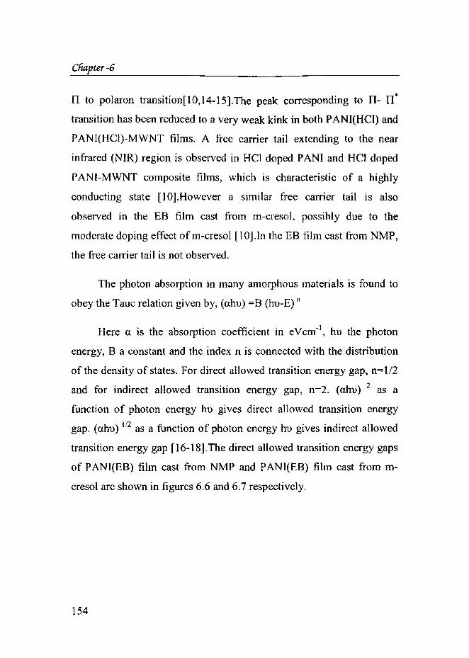
cresol are shown in figures 6.6 and 6.7 respectively.
154

Opticaltransitiongap analusis inpofgmerfilms
10000000
432o-+---.,......--,-.........,.:=--~---r----r--+--~----,
o
..-.~
lE(J
>N~ 5000000
">.c~
"-'"
Fig. 6.6 Direct allowed transition energy gap of PANI (EB) filmcast from NMP
9000000
.-.. 6000000'C"""
I
E /0/
Q)
N;;- 3000000..c~
_ ...._ i
0
0 2 4
hv(eV
Fig.6.7 Direct allowed transition energy gap of PANI (EB) filmcast from m-cresol
The direct allowed transition energy gap of PANI (EB) film cast
from NMP falls at 3.12 eV (Il- n' transition), while that corresponding
to PANI(EB) film cast from m-cresol falls at 3.0 eV and
155

Cliapter-6
2.508 eV(polaron to n' transition).The indirect allowed transition
energy gaps of PANI(EB) film cast from NMP and PANI(EB) film
cast from m-cresol are shown in figures 6.8 and 6.9.
4
3
---.....-.~
I
ECJ
2> , .>Cl)
N''-'"~
s.c~
00 2
V)
Fig. 6.8 Indirect allowed transition energy gap of PANI (EB)film cast from NMP
3
o-+--- - -..,.---rlf--7---,....----.-----,---
o
--- 40...............I
ECJ>~
~ 20>'.ct'
"-'"
2
hv(eV)
Fig. 6.9 Indirect allowed transition energy gap of PANI (EB) filmcast from m-cresol
156

Opticaltransitiongap anafgsis inpoEgmerfilms
The indirect allowed transition energy gap of PANI (EB) film
cast from NMP is at 2.38eV(n- n' transition) and that
corresponding to PANI(EB) film cast from m-cresol falls at
2.33eV(n- n' transition) and 2.05 eV(polaron to n' transition).The
obtained values closely match with those obtained for undoped
plasma polymerized PANI films[ 16].Polaron to n' transition is not
observed in PANI(EB) films cast from NMP and plasma
polymerized films of undoped PANI.The presence of polaron to n'transition in PANI(EB) film cast from m-cresol is possibly due to
the moderate doping effect of m-cresol. Obviously both the direct
allowed and indirect allowed transition energy gaps decrease for
PANI (EB) films cast from m-creso1.PANI (EB) takes up a random
coil conformation in NMP due to twist defects between aromatic
rings while such twist defects are removed in PAN I (EB) cast from
m-cresol solution. The moderate doping effect due to increased
polymer-solvent interaction in m-cresol results in more extended
conformation of polymer chains [19]. The free carrier tail in the NIR
region indicates the presence of intra band transitions within the
half-filled polaron band [10].
The direct allowed and indirect allowed transition energy gaps of
PANI (HCI) and PANI (HCI)-MWNT( I :0.5) composite films (both cast
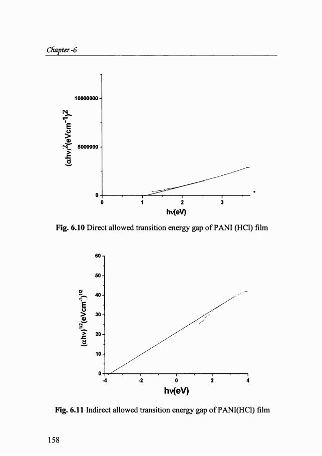
from m-cresol) are shown in figures 6.10-6.13.
157
Cliapter-6
10000000
N........t-
I
ECJ
~~ 5000000s.ct5~
32
hv(eV)
O-+---...,....---.-----.----.--~-----,...---...--
o
Fig. 6.10 Direct allowed transition energy gap of PANI (HCI) film
60
50
t!40...........
~
ECJ> 30Cl)--....s........> 20.c~--....
10
0-4 -2 o 2 4
hv(eV)
Fig. 6.11 Indirect allowed transition energy gap ofPANI(HCI) film
158

Opticaltransitiongap analysis inpofgmerfilms
900
42
hv(eV)
O~----.--...-.::;::::;;;---------------o
Fig. 6.12 Direct allowed transition energy gap of PANI(HCI)MWNT(I :0.5) composite film
60..;
50
........~~
I40 7'
E/
.-(J //> 30Cl)
"'-'"
.......~~ 20;>
t310
0-4
hv(eV)
Fig. 6.13 Indirect allowed transition energy gap of PANI (HCI)MWNT (I :0.5) composite film
159

Chapter-S
As the polaron band gets more dispersed in energy, n.n'transition becomes very weak due to the elimination of band gap
between Il band and polaron band[ 1O].In that case the transition
energy gap corresponds to that between polaron band and n' band.
The direct allowed transition energy gap of PANI(HCI) cast from
m-cresol is l.0geV while the indirect transition energy gap is
3.7eV.The direct allowed transition energy gap of PANI(HCl)
MWNT film cast from m-cresol is O.91147eV and indirect allowed
transition energy gap is -3.58eV.Negative energy gap has already
been reported in inorganic systems such as InNxSbl_x,Hgl_x_
yCdxMnyTe and HgTe-CdTe[20-23].Techniques like
XPS,HREELS,magneto phonon resistance and magneto transport
measurements have been employed to establish the presence of
negative energy gap. According to reports, in negative energy gap
materials, Valance Band Maximum (VBM) lies above Conduction
Band Minimum (CBM) [20].But we have not come across any reports
of negative energy gap in doped polymers. Since the energy band
structure of conducting polymers is different from that of
conventional inorganic semimetals, more detailed investigations are
necessary to bring out the origin of negative energy gap in doped
polymers showing semi metallic behaviour.In the present work,
negative energy gap has been observed in the indirect allowed
transitions for the HCl doped PANI and HCI doped PANI-MWNT
composite films which are in the semi metallic state(as given earlier,
the D.C electrical conductivity values of HCI doped PANI and HCI
doped PANI-MWNT composite films are lOS/cm and 40S/cm

Optial{transitiongap analusis inpofymerfilms
respectively.)[24].Both the PANI (EB) films, which are in the
insulating state, do not show any negative energy transition. The
existence of the negative energy transition is a consequence of the
semi metallic state of the polymer, which is in agreement with the
earlier observation of negative energy gap in semi metallic inorganic
systems. Moreover the negative energy transition is observed only in
the indirect allowed transition whereas it is absent in the direct
allowed transition. Thus phonons do play a significant role in the
origin of negative energy transition. The origin and nature of such a
transition in highly conducting doped polymers can be clearly
established only after detailed investigations employing more
sophisticated techniques.
6.7 Conclusions
In the indirect allowed transitions, a negative energy transition
has been observed in Hel doped PANI and Hel doped PANI-MWNT
films, both of which are in the highly conducting, semi metallic state.
Such a transition is absent in the PANI (EB) films which are in the low
conducting, insulating state. The origin of the negative energy
transition is a consequence of the semi metallic state, brought about by
phonon assisted processes. The present work extends ample scope for
future investigations in these directions, since the origin and nature of
the negative energy transition in highly conducting polymer systems
can be clearly established only after detailed investigations using more
sophisticated techniques.

Chapter-«
References
[I] K Lee, S Cho, S H Park, A J Heeger, C W Lee, S H Lee, Nature441(2006)65
[2] Y Long,Z Chen.N Wang,J Li,M Wan,PhysicaB344(2004)82
[3] E R Holland,S J Pomfret,P N Adams,A P Monkman ,J.Phys.:Condens. Matter8( 1996)2991
[4] A Mirmohseni, G G Wallace, Polymer44 (2003)3523
[5] R Murugesan,E Subramanian,Bull.Mater.Sci26(2003)529
[6] H Liu,X B Hu,J Y Wang,R I Boughten, Macromolecules35(2002)9414
[7] Y Cao,P Smith,A J Heeger,Synth.Met48( 1992)91
[8J Y Geng,J Li,Z Sun,X Jing, F Wang,Synth.Met96(1998)1
[9] J Tang,X Jing,B Wang,F Wang,Synth.Met24(l988)23 1
[IOJ D L Wise,G E Wnek,D J Trantalo,T M Cooper,J D Gresser(Eds),Electrical and optical polymer systems Fundamentals, Methods and
Applications, Marcel Dekker, INC.Newyork,1998,p359-386
[11J P Rannou, A Pron, M Nechtscheim, Synth.Met.! 0 I (1999)827
[12] H Lirn, J H Choi, J.Chern.PhysI24 (2006)014710
[13] J K Avlyanov, Y Min, A G MacDiarmid, Synth.Met. 72(1995)65
[14] S Stafstrorn, J L Bredas, A J Epstein, H S Woo, D B Tanner, W S
Huang, A G MacDiarmid,Phys.Rev.Lett.,59(1987)1464
[15] N C Baird, H Wang, Chern.Phys.Lett.202 (1993)50
[16] C Joseph Mathai, S Saravanan, M R Anantharaman, S Venkitachalam,S Jayalekshmi, J.Phys.D:Appl.Phys35 (2002)2206
[17] J Tauc, Optical properties of solids, A Ables, North-Holland,
Amsterdam, 1970, p277

Opticaltransitiongap anafgsis inpofymerfilms
[18] EA Davis, N F Mott, phil.Mag.22 (1970)903
[19] Y Xia, A G MacDiannid, A J Epstein, Macromolecules27 (1994) 7212
[20] T D Veal, I Mahboob, C F McConville, Phys.Rev.Lett92
(2004) 136801
[21] S Kuroda, T Okamoto, H J Kwon, K Takita, Semicond. Sci.
Technol. 7 (1992) 842
[22] C A Hoffman, J R Meyer, F J Bartoli, Y Lansari, J W CrookJr., J FSchetzina, Phys.Rev8 40(6)(1989)3867
[23] C Y Moon, S-H Wei, Phys.Rev.B74 (2006)045205
[24] M.Amrithesh, K.P.Chandni, S.Jayalekshmi, Febin Kurian,s.r.Varma, Optoelectron.Adv.Mater (RC), 3(2) (2009) 149
••.•••• roc;:Q ..


![Lecture on Intrinsically conducting polymers on textiles [EN] · Conducting polymers • Intrinsically conducting polymers (ICPs) are π-conjugated organic polymers able to conduct](https://img.pdfslide.net/doc/110x75/5f07a9317e708231d41e19a9/lecture-on-intrinsically-conducting-polymers-on-textiles-en-conducting-polymers.jpg)