Embed Size (px)
Citation preview

I/O Wiring andSpecifications

Get
ting
Sta
rted
I/O W
iring
and
Spe
cific
atio
ns3–2
I/O Wiring and Specifications
I/O Wiring Strategies
The DL405 system is very flexible and will work in many different wiringconfigurations. By studying this section before actual installation, you should find thebest wiring strategy for your application . This will help to lower system cost, wiringerrors, and avoid safety problems.DL405 system circuitry is divided into three main regions separated by isolationboundaries, shown in the drawing below. Electrical isolation provides safety, so thata fault in one area does not damage another. A transformer in the power supplyprovides magnetic isolation between the primary and secondary sides.Opto-couplers provide optical isolation in Input and Output circuits. This isolateslogic circuitry from the field side, where factory machinery connects. Note that thediscrete inputs are isolated from the discrete outputs, because each is isolated fromthe logic side. Isolation boundaries protect the operator interface (and the operator)from power input faults or field wiring faults. When wiring a DL405 system, it isextremely important to avoid making external connections that connect logic sidecircuits to any other.
CPU
InputModuleMain
PowerSupply
Inputs
Outputs
Power Input
OutputModule
Primary Side Secondary, or Logic side Field Side
DL405 System
Programming Device,Operator Interface, or Network
IsolationBoundary
IsolationBoundary
(backplane)
(backplane)
The next figure shows the physical layout of a DL405 system, as viewed from thefront. In addition to the basic circuits covered above, AC-powered units include anauxiliary +24VDC power supply with its own isolation boundary. Since the supplyoutput is isolated from the other three circuits, it can power input and/or outputcircuits!
Input Module
CPU
Comm.
MainPowerSupply
Auxiliary+24VDCSupply
To ProgrammingDevice, Operator
Inputs Commons CommonsOutputs
+24VDC Out
Power Input
SystemDL405
Interface, Network
Output Module
InternalBackplane
Supply forOutput Circuit
Primary Side Secondary, orLogic side
Field Side
DL405 SystemIsolationBoundaries

Getting S
tartedI/O
Wiring and
Specifications
3–3I/O Wiring and Specifications
In some cases, using the built-in auxiliary +24VDC supply can result in a costsavings for your control system. It can power combined loads up to 400 mA. Becareful not to exceed the current rating of the supply. If you are the system designerfor your application, you may be able to select and design in field devices which canuse the +24VDC auxiliary supply.In most applications it will be necessary to power the input devices from one powersource, and to power output loads from another source. Loads often requirehigh-energy AC power, while input sensors use low-energy DC. If a machineoperator is likely to come in close contact with input wiring, then safety reasons alsorequire isolation from high-energy output circuits. It is most convenient if the loadscan use the same power source as the DL405 system, and the input sensors can usethe auxiliary supply, as shown to the left in the figure below.If the loads cannot be powered from the system supply, then a separate supply mustbe used as shown to the right in the figure below.
!"#$%
&' DL405 System
(
AC Power
+ –
!"#$%
&' DL405 System
(
AC Power
+ –
LoadSupply
A worst-case scenario, from a cost and complexity view-point, is an applicationwhich requires separate power sources for the DL405 system, input devices, andoutput loads. The example wiring diagram below on the right shows how this canwork, but also that the auxiliary supply output is an unused resource.
!"#$%
&' DL405 System
(
AC Power
+ –
LoadSupply
InputSupply
Powering I/OCircuits UsingSeparate Supplies

Get
ting
Sta
rted
I/O W
iring
and
Spe
cific
atio
ns3–4
I/O Wiring and Specifications
This next section helps to provide a solid understanding of “sinking” and “sourcing”concepts. Use of these terms occurs frequently in input or output circuit discussions.It is the goal of this section to make these concepts easy to understand, furtherensuring success in installation.
Sinking = provides a path to supply ground (–)Sourcing = provides a path to supply source (+)
Sinking and sourcing terminology only applies to DC input and output circuitsbecause of the reference to (+) and (–) polarities. Input and output points that aresinking or sourcing only can conduct current in only one direction. This means it ispossible to connect the external supply and field device to the I/O point with currenttrying to flow in the wrong direction, and the circuit will not operate. However, you cansuccessfully connect the supply and field device every time by understanding“sourcing” and “sinking”.
For example, the figure to the rightillustrates a “sinking” input. To properlyconnect the external supply, we just haveto connect it so the input provides a path toground (–). Start at the DL405 systeminput terminal, follow through the inputsensing circuit, exit at the commonterminal, and connect the supply (–) to thecommon terminal. By adding the switch,between the supply (+) and the input, wehave completed the circuit. Current flowsin the direction of the arrow when theswitch is closed.
+
–
InputSensing
%(#)*
+,-
By applying the circuit principle above to the four possible combinations ofinput/output sinking/sourcing types, you have the four circuits as shown below. TheI/O module specifications at the end of this chapter list the input or output type.
+
–
InputSensing
(
Sinking Input Sinking Output
Sourcing Input Sourcing Output
%(#)*
+
–
OutputSwitch
%(#)*
+
–
InputSensing
(
%(#)*
+
–
OutputSwitch
%(#)*
Sinking / SourcingConcepts

Getting S
tartedI/O
Wiring and
Specifications
3–5I/O Wiring and Specifications
In order for an I/O circuit to operate,current must enter at one terminal and exitat another. This means at least twoterminals are associated with every I/Opoint. In the figure to the right, the Input orOutput terminal is the main path for thecurrent. One additional terminal mustprovide the return path to the powersupply.
+
–
I/OCircuit
%(#)*
(I/O Point)
. &
FieldDevice
&
If there was unlimited space and budgetfor I/O terminals, then every I/O pointcould have two dedicated terminals as thefigure above shows. However, providingthis level of flexibility is not practical oreven necessary for most applications.Most Input or Output points are in groupswhich share the return path (calledcommons). The figure to the right shows agroup (or bank) of 4 input points whichshare a common return path. In this way,the four inputs require only five terminalsinstead of eight.
+
–
InputSensing
%(#)*
#
/
"
0
NOTE: In the circuit above, the current in the common path is 4 times any channel’sinput current when all inputs are energized. This is important in output circuits whereheavier gauge wire is sometimes necessary on commons.
Most DL405 input and output modulesgroup their I/O points into banks that sharea common return path. The best indicationof I/O common grouping is on the wiringlabel, such as the one shown to the right.The miniature schematic shows two circuitbanks with eight input points in each. Thecommon terminal for each is labeled “CA”and “CB”, respectively.In the wiring label example, the positiveterminal of a DC supply connects to thecommon terminals. Some symbols youwill see on the wiring labels, and theirmeanings are:
0123
4567
ATB
12–24VDC
D4–16ND2
0123
4567
B
INPUT
CA04152637
CB40516273
10.2–26.4VDC4–12mA
L
%
' (
%
!1
I/O “Common”Terminal Concepts

Get
ting
Sta
rted
I/O W
iring
and
Spe
cific
atio
ns3–6
I/O Wiring and Specifications
In the previous section on Sourcing and Sinking concepts, we explained that DC I/Ocircuits sometimes will only allow current to flow one way. This is also true for many ofthe field devices which have solid-state (transistor) interfaces. In other words, fielddevices can also be sourcing or sinking. When connecting two devices in a seriesDC circuit, one must be wired as sourcing and the other as sinking.Several DL405 DC input modules are flexible in that they detect current flow in eitherdirection, so they can be wired as either sourcing or sinking. In the following circuit, afield device has an open-collector NPN transistor output. It sinks current from theinput point, which sources current. The power supply can be the +24 auxiliary supplyor another supply (+12 VDC or +24VDC), as long as the input specifications are met.
Field Device
+–
DL405 System DC Input
+,- + -
In the next circuit, a field device has an open-emitter PNP transistor output. Itsources current to the input point, which sinks the current back to ground. Since thefield device is sourcing current, no additional power supply is required.
Field DeviceDL405 System DC Input
+ -
!$
+,-
Sometimes an application requires connecting an output point to a solid state inputon a device. This type of connection is usually made to carry a low-level controlsignal, not to send DC power to an actuator.Several of the DL405 DC output modules are the sinking type. This means that eachDC output provides a path to ground when it is energized. In the following circuit, theoutput point sinks current to the output common when energized. It is connected to asourcing input of a field device input.
Field Device
Output
Ground
Input
Common
+V
DL405 System DC Sinking Output
+DC pwr
+
–
(sourcing)(sinking)
Power
10–30 VDC
Connecting DC I/Oto “Solid State”Field Devices
Solid StateInput Sensors
Solid StateOutput Loads

Getting S
tartedI/O
Wiring and
Specifications
3–7I/O Wiring and Specifications
In the next example a sinking DC output point is connected to the sinking input of afield device. This is different, because both the DL405 system output and field deviceinput are sinking type. Since the circuit must have one sourcing and one sinkingdevice, a sourcing capability is added to the system output by using a pull-upresistor. In the circuit below, connect Rpull-up from the output to the DC output circuitpower input.
Field Device
Output
Ground
Input
Common
DL405 System DC Output
+DC pwr
+
–
(sourcing)
(sinking)
Power
(sinking)
pull-up
Supply
R
inputR
NOTE 1: DO NOT attempt to drive a heavy load (>25 mA) with this pull-up methodNOTE 2: Using the pull-up resistor to implement a sourcing output has the effect ofinverting the output point logic. In other words, the field device input is energizedwhen the DL405 system output is OFF, from a ladder logic point-of-view. Your ladderprogram must comprehend this and generate an inverted output. Or, you maychoose to cancel the effect of the inversion elsewhere, such as in the field device.
It is important to choose the correct value of R pull-up. In order to do so, the nominalinput current to the field device (I input) when the input is energized needs to beidentified. If this value is not known, it can be calculated as shown (a typical value is15 mA). Then use I input and the voltage of the external supply to compute R pull-up.Next calculate the power Ppull-up (in watts), in order to size R pull-up properly.
2. input.3$ 1 )4
1
input
input 3 + 1-$
input.
2& 3$
"
pullup.
The easiest way to drive a sinking input field device as shown below is to use a DCsourcing output module. The Darlington NPN stage will have about 1.5 V ON-statesaturation, but this is not a problem with low-current solid-state loads.
Field Device
DL405 System DC Sourcing Output
!% '
+
–
+ -
+,-
input.

Get
ting
Sta
rted
I/O W
iring
and
Spe
cific
atio
ns3–8
I/O Wiring and Specifications
Four output modules in the DL405 I/O family feature relay outputs: D4–08TR,F4–08TRS–1, F4–08TRS–2, D4–16TR. Relays are best for the followingapplications:
Loads that require higher currents than the solid-state outputs candeliver
Cost-sensitive applications Some output channels need isolation from other outputs (such as when
some loads require different voltages than other loads)Some applications in which NOT to use relays:
Loads that require currents under 10 mA Loads which must be switched at high speed or heavy duty cycle
Relay outputs in the DL405 outputmodules are available in two contactarrangements, shown to the right. TheForm A type, or SPST (single pole, singlethrow) type is normally open and is thesimplest to use. The Form C type, orSPDT (single pole, double throw) type hasa center contact which moves and astationary contact on either side. Thisprovides a normally closed contact and anormally open contact.Some relay output module’s relays sharecommon terminals, which connect to thewiper contact in each relay of the bank.Other relay modules have relays whichare completely isolated from each other. Inall cases, the module drives the relay coilwhen the corresponding output point is on.
Relay with Form A contacts
Relay with Form C contacts
Relay contacts wear according to the amount of relay switching, amount of sparkcreated at the time of open or closure, and presence of airborne contaminants.However, there are some steps you can take to help prolong the life of relay contacts:
Switch the relay on or off only when the application requires it. If you have the option, switch the load on or off at a time when it will
draw the least current. Take measures to suppress inductive voltage spikes from inductive DC
loads such as contactors and solenoids (circuit given below).
Inductive Field Device
+ –
DL405 Relay Output
.
Relay OutputGuidelines
Prolonging RelayContact Life

Getting S
tartedI/O
Wiring and
Specifications
3–9I/O Wiring and Specifications
Adding external contact protection may extend relay life beyond the number ofcontact cycles listed in the specification tables for relay modules. High currentinductive loads such as clutches, brakes, motors, direct-acting solenoid valves, andmotor starters will benefit the most from external contact protection.The RC network must be located close to the relay module output connector. To findthe values for the RC snubber network, first determine the voltage across thecontacts when open, and the current through them when closed. If the load supply isAC, then convert the current and voltage values to peak values:
R () 3C (F) =10
I2
V
10 x I x, where x=
50
V1 +
C minimum = 0.001 F, the voltage rating of C must be V, non-polarizedR minimum = 0.5 , 1/2 W, tolerance is 5%
For example; a relay contact drives a load at 120VAC, 1/2 A. Since this example hasan AC power source, first, calculate the peak values:
Ipeak = Irms x 1.414, = 0.5 x 1.414 = 0.707 Amperes
Vpeak = Vrms x 1.414 = 120 x 1.414 = 169.7 Volts
Now, finding the values of R and C:
R () 3
C (F) =10
I2
V
10 x I x, where x=
50
V1 +
=10
0.7072
= 0.05 F, voltage rating 170 Volts
x=50
169.71 + = 1.29 R () 3
169.7
10 x 0.707 1.293 05 6 0" 6 5%
If the contact is switching a DC inductive load, add a diode across the load as near toload coil as possible. When the load is energized the diode is reverse-biased (highimpedance). When the load is turned off, energy stored in its coil is released in theform of a negative-going voltage spike. At this moment the diode is forward-biased(low impedance) and shunts the energy to ground. This protects the relay contactsfrom the high voltage arc that would occur just as the contacts are opening.For best results, follow these guidelines in using a noise suppression diode:
DO NOT use this circuit with an AC power supply. Place the diode as close to the inductive field device as possible. Use a diode with a peak inverse voltage rating (PIV) at least 100 PIV, 3A
forward current or larger. Use a fast-recovery type (such as Schottkytype). DO NOT use a small-signal diode such as 1N914, 1N941, etc.
Be sure the diode is in the circuit correctly before operation. If installedbackwards, it short-circuits the supply when the relay energizes.

Get
ting
Sta
rted
I/O W
iring
and
Spe
cific
atio
ns3–10
I/O Wiring and Specifications
I/O Module Wiring and Specifications
Before wiring the I/O modules in yoursystem to field devices, it’s very importantto make sure each I/O module is in theright slot and base in the system. Costlywiring errors may be avoided by doing thefollowing:
? Perform the power budget calculations for each base to verify the base
power supply can power all the modules in the base. Whenever possible, keep modules with high voltage and current wiring
away from sensitive analog modules.
NOTE: Please refer to the applicable Base Controller User manual for the powerbudget requirements and worksheets.
The diagram below shows the status indicator location for common I/O modules.
Display status
Blown fuse(non-replaceable)
indicator
Loose terminalblock indicator
Status indicators
(selects a groupof signals to
be displayed)
Wire tray
(Output modules only)
The DL405 family of I/O modules have acolor-coded stripe on the front bezel tohelp identify whether the module type isinput, output, or special module. The colorcode description is listed below:
0
1
2
3
4
5
6
7
A
TB
110VAV
D4–16NA
0
1
2
3
4
5
6
7
B
INPUT
CA
0
80–132VAC
80–20mA
50/60Hz
Color Bar
Module Type% 7% 7
Color Code.8
Module Placement
I/O ModuleStatus Indicators
Color Codingof I/O Modules

Getting S
tartedI/O
Wiring and
Specifications
3–11I/O Wiring and Specifications
You must first remove the front cover of the module prior to wiring. To remove thecover depress the bottom tab of the cover and tilt the cover up to loosen from themodule.All DL405 I/O module terminal blocks are removable for your convenience. Toremove the terminal block loosen the retaining screws and and lift the terminal blockaway from the module. When you return the terminal block to the module make surethe terminal block is tightly seated. Be sure to tighten the retaining screws. Youshould also verify the loose terminal block LED is off when system power is applied.
WARNING: For some modules, field device power may still be present on theterminal block even though the system is turned off. To minimize the risk of electricalshock, disconnect all field device power before you remove the connector.
Push tab andlift to remove
Retaining screwTerminal screws
Retaining screw
Loose terminal blockLED indicator
I/O modulewiring tray
Wiring a Modulewith a TerminalBlock

Get
ting
Sta
rted
I/O W
iring
and
Spe
cific
atio
ns3–12
I/O Wiring and Specifications
The 32 point and 64 point modules use a different style of connector due to theincreased number of I/O points. There are two types of connectors used with thehigher density modules. One is a D-shell connector, which requires soldering. Theother is a ribbon cable type of connector which simply crimps onto a ribbon cable.
For the 64 point modules, you must either use ribbon cable connectors, or specialsolder type connectors designed specifically for the 64 point modules. Order partnumber D4–IO3264S, which includes 2 solder-type connectors in the pack, or orderD4–IO32R, which contains 2 ribbon cable type connectors in the pack.
NOTE: For another alternative wiring solution, consider usingAutomationdirect.com’s ZIPLink Connection systems. The ZIPlink cables plugdirectly into a Automationdirect.com I/O module. The opposite end is connected to aZIPlink connector module. Please refer to our catalog for more information on theseproducts.
32 pt. Module
Ribbon connector
Ribbon cable
Terminal block
OR
D-sub type connector
64pt. Module
Wiring a Moduleusing a RibbonCable/Solder TypeConnector

Getting S
tartedI/O
Wiring and
Specifications
3–13I/O Wiring and Specifications
Both types of connectors are available from Automationdirect.com. These sameconnectors are also available from other Fujitsu Microelectronics, Inc. Use thefollowing part numbers to order these connectors.Automationdirect.com Part Numbers
D4–IO3264R — Ribbon cable connectors, 2 in a pack. Can be used oneither 32 point or 64 point modules.
D4–IO3264S — Solder type connector, 2 in a pack. Can be used oneither 32 point or 64 point modules.
Fujitsu Part NumbersFor connectors made by Fujitsu, you may contact Fijitsu at the following address:Fujitsu Microelectronics, Inc.Electronic Components Division3545 North First StreetSan Jose, CA 95134–1804 USA408–922–9000
FCN–367J040–AU/F, or –AG/F — 32 / 64 point ribbon cable connector FCN–361J040–AU, or –AG — 32 / 64 point solder type connector
(AU connectors use gold over palladium plating. AG connectors use silver plating.)
If you wish to use a terminal block with your 32 or 64 point module, here is a partial listof vendors who can provide the parts you will need to build the configuration shownearlier consisting of a ribbon cable, a ribbon cable connector and a terminal block.
Vendors
3M Electronic Products Division6801 River Place Blvd.Austin, TX 78726–9000800–225–5373
DuPont Connector SystemsBarley Mill PlazaWilmington, DE 19898–0019800–237–2374
Augat/RDI525 Randy Rd.Carol Stream, IL 60188708–682–4100
Phoenix Contacts ProductsP.O. Box 4100Harrisburg, PA 17111–0100717–944–1300
AMP IncorporatedP.O. Box 3608Harrisburg, PA 17105–3608717–564–0100
Thomas & Betts Electronics Div.200 Executive Center DriveGreenville, SC 29616803–676–2900
Cooper Industries, Belden Div.P.O. Box 1980Richmond, IN 47375317–983–5200
Weidmuller, Inc.821 Southlake Blvd.Richmond, VA 23236804–794–2877
Newark Electronics4108 North Ravenswood Ave.Chicago, Il 60640312–784–5100
(Newark Electronics is a distributorfor all of the above product manufac-turers except for Phoenix ContactsProducts)
Part Numbers forModuleConnectors
Vendors For theParts Used in theTerminal BlockConfiguration
Get
ting
Sta
rted
I/O W
iring
and
Spe
cific
atio
ns3–14
I/O Wiring and Specifications
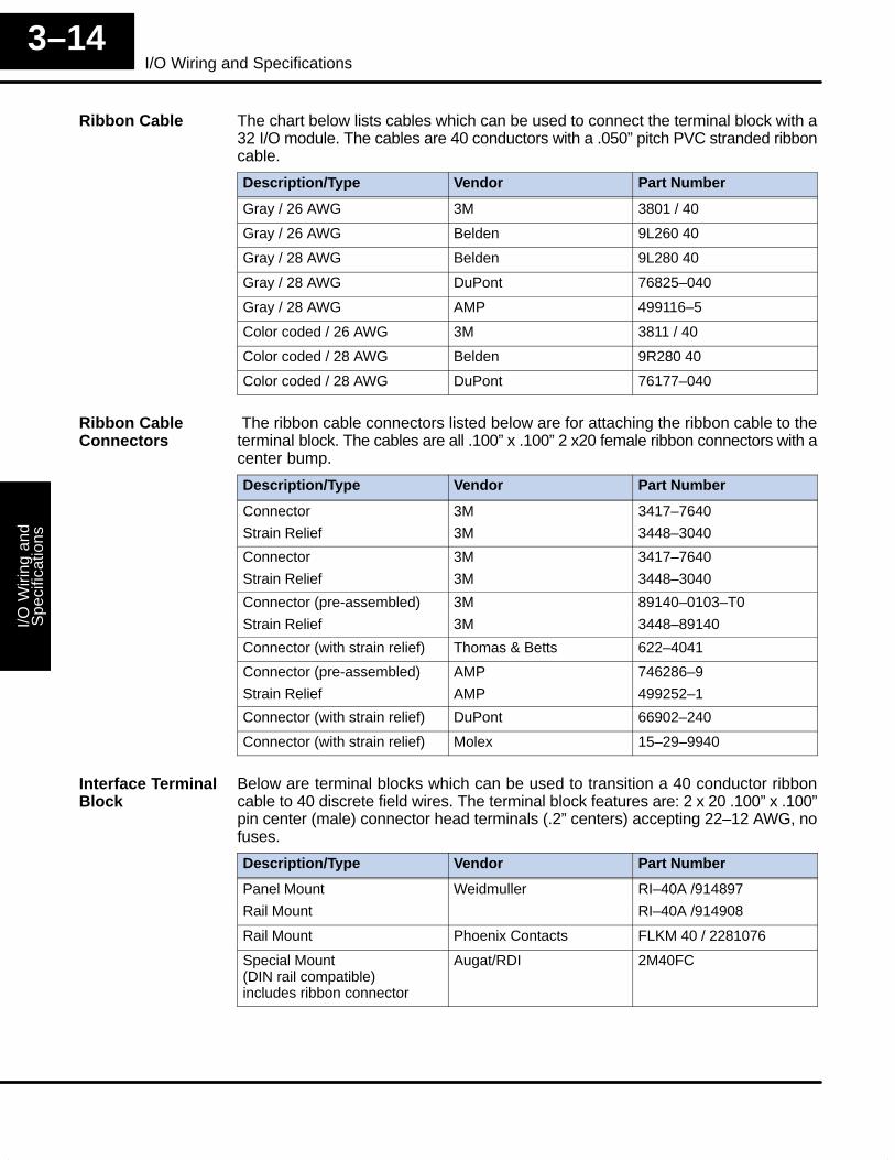
The chart below lists cables which can be used to connect the terminal block with a32 I/O module. The cables are 40 conductors with a .050” pitch PVC stranded ribboncable.
Description/Type Vendor Part Number
Gray / 26 AWG 3M 3801 / 40
Gray / 26 AWG Belden 9L260 40
Gray / 28 AWG Belden 9L280 40
Gray / 28 AWG DuPont 76825–040
Gray / 28 AWG AMP 499116–5
Color coded / 26 AWG 3M 3811 / 40
Color coded / 28 AWG Belden 9R280 40
Color coded / 28 AWG DuPont 76177–040
The ribbon cable connectors listed below are for attaching the ribbon cable to theterminal block. The cables are all .100” x .100” 2 x20 female ribbon connectors with acenter bump.
Description/Type Vendor Part Number
Connector
Strain Relief
3M
3M
3417–7640
3448–3040
Connector
Strain Relief
3M
3M
3417–7640
3448–3040
Connector (pre-assembled) 3M 89140–0103–T0( )
Strain Relief 3M 3448–89140
Connector (with strain relief) Thomas & Betts 622–4041
Connector (pre-assembled) AMP 746286–9( )
Strain Relief AMP 499252–1
Connector (with strain relief) DuPont 66902–240
Connector (with strain relief) Molex 15–29–9940
Below are terminal blocks which can be used to transition a 40 conductor ribboncable to 40 discrete field wires. The terminal block features are: 2 x 20 .100” x .100”pin center (male) connector head terminals (.2” centers) accepting 22–12 AWG, nofuses.
Description/Type Vendor Part Number
Panel Mount Weidmuller RI–40A /914897
Rail Mount RI–40A /914908
Rail Mount Phoenix Contacts FLKM 40 / 2281076
Special Mount (DIN rail compatible) includes ribbon connector
Augat/RDI 2M40FC
Ribbon Cable
Ribbon CableConnectors
Interface TerminalBlock
Getting S
tartedI/O
Wiring and
Specifications
3–15I/O Wiring and Specifications
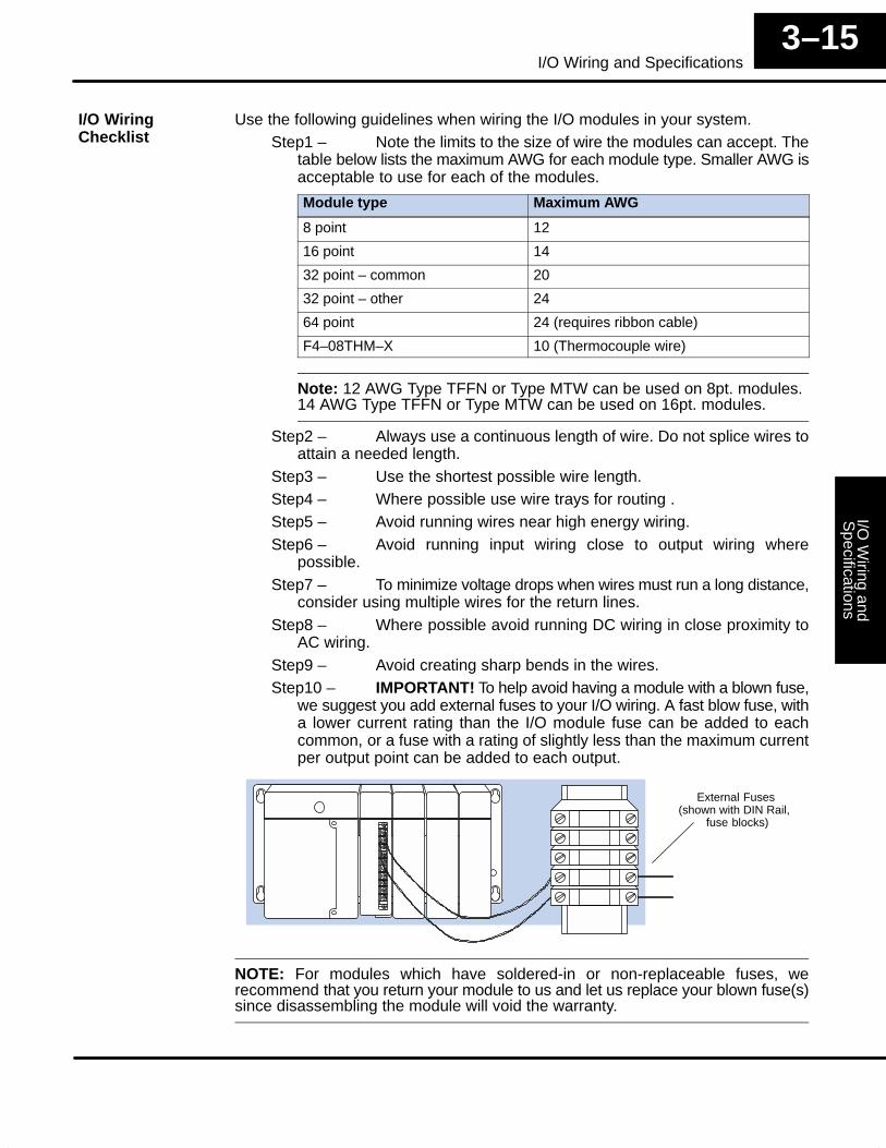
Use the following guidelines when wiring the I/O modules in your system.Step1 – Note the limits to the size of wire the modules can accept. The
table below lists the maximum AWG for each module type. Smaller AWG isacceptable to use for each of the modules.
Module type Maximum AWG
8 point 12
16 point 14
32 point – common 20
32 point – other 24
64 point 24 (requires ribbon cable)
F4–08THM–X 10 (Thermocouple wire)
Note: 12 AWG Type TFFN or Type MTW can be used on 8pt. modules.14 AWG Type TFFN or Type MTW can be used on 16pt. modules.
Step2 – Always use a continuous length of wire. Do not splice wires toattain a needed length.
Step3 – Use the shortest possible wire length.Step4 – Where possible use wire trays for routing .Step5 – Avoid running wires near high energy wiring.Step6 – Avoid running input wiring close to output wiring where
possible.Step7 – To minimize voltage drops when wires must run a long distance,
consider using multiple wires for the return lines.Step8 – Where possible avoid running DC wiring in close proximity to
AC wiring.Step9 – Avoid creating sharp bends in the wires.Step10 – IMPORTANT! To help avoid having a module with a blown fuse,
we suggest you add external fuses to your I/O wiring. A fast blow fuse, witha lower current rating than the I/O module fuse can be added to eachcommon, or a fuse with a rating of slightly less than the maximum currentper output point can be added to each output.
External Fuses(shown with DIN Rail,
fuse blocks)
NOTE: For modules which have soldered-in or non-replaceable fuses, werecommend that you return your module to us and let us replace your blown fuse(s)since disassembling the module will void the warranty.
I/O WiringChecklist

Get
ting
Sta
rted
I/O W
iring
and
Spe
cific
atio
ns3–16
I/O Wiring and Specifications
The following table lists the available DL405 input modules.
DL405Input Module Type
Number ofInput Points
DC CurrentSink Input
DC CurrentSource Input
AC Input
D4–16ND2 16
D4–16ND2F 16
D4–32ND3–1 32
D4–32ND3–2 32
D4–64ND2 64
D4–08NA 8
D4–16NA (–1) 16
D4–16NE3 16
F4–08NE3S 8
D4–08ND3S 8
The following table lists the available DL405 output modules. Specifications beginafter the input modules’ specifications.
DL405 Output Module Type
Number ofOutput Points
DC CurrentSink Output
DC CurrentSourceOutput
AC Output
D4–08TD1 8
F4–08TD1S 8
D4–16TD1 16
D4–16TD2 16
D4–32TD1 32
D4–32TD1–1 32
D4–32TD2 32
D4–64TD1 64
D4–08TA 8
D4–16TA 16
D4–08TR 8
F4–08TRS–1 8
F4–08TRS–2 8
D4–16TR 16
DL405 DiscreteInput Module Chart
DL405 DiscreteOutput ModuleChart

Getting S
tartedI/O
Wiring and
Specifications
3–17I/O Wiring and Specifications
Specification F4–08THM–n F4–08RTD
Channels 8 8
Input Ranges Type E: –270/1000C (–450/1832F)Type J: –210/760C (–350/1390F)Type K: –270/1370C (–450/2500F)Type R: 0/1768C (–32/3214F)Type S: 0/1768C (–32/3214F)Type T: –270/400C (–450/752F)Type C: 0/2320C (–32/4208F)Type B: 141/1820C (286/3594F)Type P: –99/1395C (–146/2543F)–1: 0 to 50mV–2: 0 to 100mV–3: 0 to 25mV
Pt100Ω: –200.0/850.0C (–328/ 562F)Pt1000Ω: –200.0/595.0C (–328/1103F)jPt100Ω: –38.0/450.0C (–36/842F)
Cu. 25Ω, Cu. 10Ω: –200.0/260.0C (–328/500F)
Resolution 12 bit (1 in 4096) 15 bit (1 in 32768)
Maximum Inaccuracy 1° C type J,K,E,T thermocouples3° C type R,S,B,C,P thermocouples
0.2% at 25°C (77°F)
Specification F4–08THM
Channels 8
Input Ranges Type J: –190/760C (–310/1400F)Type E: –210/1000C (–346/1832F)Type K: –150/1372C (–238/2502F)Type R: 65/1768C (149/3214F)Type S: 65/1768C (149/3214F)Type T: –230/400C (–382/752F)Type B: 529/1820C (984/3308F)Type N: –70/1300C (–94/2372F)Type C: 65/2320C (149/4208F)–1: 0 to 50mV–2: 0 to 100mV–3: 0 to 25mV
Resolution 16 bit (1 in 65535)
Maximum Inaccuracy 3° C (excluding thermocouple error)
Specification F4–04AD F4–04ADS F4–08AD
Channels 4 4 8
Input Ranges 0–20 mA, 4–20 mA,1–5V, 0–5V, 0–10V,5V, 10V
0–20 mA, 4–20 mA,1–5V, 0–5V, 0–10V,5V, 10V
0–20 mA, 4–20 mA,1–5V, 0–5V, 0–10V,5V, 10V
Resolution 12 bit (1 in 4096) 12 bit (1 in 4096) 12 bit (1 in 4096)
Input Type Single ended Isolated Single ended
Maximum Inaccuracy 0.4% at 25°C (77°F)0.55% at 0° to 60° C (32° to 140°F)
0.4% at 25°C (77°F)0.7% at 0° to 60°C (32° to 140°F)
0.3% at 25°C (77°F)0.5% at 0° to 60°C (32° to 140°F)
Special InputModule Chart
Special InputModule Chart
Analog InputModule Chart

Get
ting
Sta
rted
I/O W
iring
and
Spe
cific
atio
ns3–18
I/O Wiring and Specifications
Specification D4–02DA F4–04DA F4–04DA–1
Channels 2 4 4
Output Ranges 4–20 mA, 1–5V, 0–10V 4–20 mA, 0–5V, 0–10V,5V, 10V
4–20mA
Resolution 12 bit (1 in 4096) 12 bit (1 in 4096) 12 bit (1 in 4096)
Output Type Independent Single ended Single ended
MaximumInaccuracy
0.2% at 25°C (77°F)
0.5% at 60°C (unipo.)0.7% at 60°C (bipol.)0.8% at 60°C (curr.)
0.1 % at 25°C (77°F)0.3 % at 0 to 60°C
(32 to 140°F)
Specification F4–04DA–2 F4–08DA–1 F4-16DA-1
Channels 4 8 16
Output Ranges 0–5V, 0–10V, 5V,10V
4–20mA 4–20 mA
Resolution 12 bit (1 in 4096) 12 bit (1 in 4096) 12 bit (1 in 4096)
Output Type Single ended Single ended Single ended
Maximum Inaccuracy
0.2 % at 25°C (77°F) 0.4% at 0° to 60°C
(32° to 140°F)
0.2% at 25°C (77°F)0.4% at 0° to 60°C
(32° to 140°F)
0.2 % at 25°C (77°F)0.4 % at 0° to 60°C
(32° to 140°F)
Specification F4–04DAS–1 F4–08DA–2 F4-16DA-2
Channels 4 8 16
Output Ranges 4–20 mA 0–5v, 0–10v 0–5v, 0–10v,Combination of both
Resolution 16 bit (1 in 65536) 12 bit (1 in 4096) 12 bit (1 in 4096)
Output Type Single ended Single ended Single ended
Maximum Inaccuracy
0.07 % at 25°C(77°F) 0.18% at 0° to 60°C
(32° to 140°F)
0.2% at 25°C (77°F)0.4% at 0° to 60°C
(32° to 140°F)
0.2 % at 25°C (77°F)0.4 % at 0° to 60°C
(32° to 140°F)
Analog OutputModule Chart

Getting S
tartedI/O
Wiring and
Specifications
3–19I/O Wiring and Specifications
Glossary of Specification TermsInputs or Outputs PerModule
Indicates number of electrical input or output points per module and designatescurrent sinking, current sourcing, or either.
Commons Per Module Number of electrical commons per module. A common is a connection to an inputor output module which is shared by multiple I/O circuits. It is ususally in the returnpath to the power supply of the I/O circuit.
Input Voltage Range The operating voltage range of an input circuit, measured from an input point to itscommon terminal, when the input is ON.
Output Voltage Range The output voltage range of an output circuit, measured from an output point to itscommon terminal, when the output is OFF.
Peak Voltage Maximum voltage allowed for an input or output circuit for a short duration.
AC Frequency AC modules are designed to operate within a specific frequency range.
ON Voltage Level The minimum voltage level at which an input point will turn ON.
OFF Voltage Level The maximum voltage level at which an input point will turn OFF.
Input Impedance The electrical resistance measured between an input point and its common point.Since this resistance is non-linear, it may be listed for various input currents.
Input Current Typical operating current for an active (ON) input.
Minimum ON Current The minimum current for the input circuit to operate reliably in the ON state.
Maximum OFF Current The maximum current for the input circuit to operate reliably in the OFF state.
Minimum Load The minimum load current required for an output circuit to operate properly.
External DC Required Some output modules require external power for the output circuitry.
On Voltage Drop Sometimes called “saturation voltage”, it is the voltage measured from an outputpoint to its common terminal when the output is ON, at max. load.
Maximum LeakageCurrent
The maximum current a connected maximum load will receive when the outputpoint is OFF.
Maximum Inrush Current The maximum current used by a load for a short duration upon an OFF to ONtransition of a output point. It is greater than the normal ON state current and ischaracteristic of inductive loads in AC circuits.
Base Power Required The +5VDC power from the base required to operate the module. Be sure toobserve the base power budget calculations.
OFF to ON Response The time the module requires to process an OFF to ON state transition.
ON to OFF Response The time the module requires to process an ON to OFF state transition.
Status Indicators The LEDs that indicate the ON/OFF status of an input or output point. These LEDsare electrically located on the logic (CPU) side of the I/O interface circuit.
Terminal Type Indicates whether the module’s connector is removable or non-removable.
Weight Indicates the weight of the module.
Fuses Protective device for an output circuit, which stops current flow when currentexceeds the fuse rating current. It may be replaceable or non-replaceable, orlocated externally or internally.

Get
ting
Sta
rted
I/O W
iring
and
Spe
cific
atio
ns3–20
I/O Wiring and Specifications
D4–08ND3S DC Input D4–16ND2 DC InputInputs per module 8 (sink/source) Inputs per module 16 (current sourcing)
Commons per module 8 (isolated) Commons per module 2 (isolated)
Input voltage range 20–52.8VDC Input voltage range 10.2–26.4VDC
Peak voltage 52.8VDC Peak voltage 26.4VDC
ON voltage level >18 V ON voltage level > 9.5VDC
OFF voltage level < 7V OFF voltage level < 4.0 VDC
Input impedance 4.8 K Input impedance 3.2 K @ 12VDC2.9 K @24VDC
Input current @ 24 / 48 VDC 5 mA / 10 mA Input current @ 12 / 24VDC 3.8 mA / 8.3 mA
Minimum ON current 3.5 mA Minimum ON current 3.5 mA
Maximum OFF current 1.5 mA Maximum OFF current 1.5 mA
Base power required 5V 100 mA max Base power required 5V 150 mA max
OFF to ON response 3–10 ms OFF to ON response 1–7 ms (2.3 typical)
ON to OFF response 3–12 ms ON to OFF response 2–12 ms (4.6 typical)
Terminal type Removable Terminal type Removable
Status indicators Logic Side Status indicators Logic Side
Weight 8.8 oz. (250 g) Weight 8.8 oz. (250 g)
0123
4567
TB
24–48VDC
D4–08ND3S
INPUT
C0
0
20–52.8VDC4–12mA
C1
1
C2
2
C3
3
C4
4
C5
5
C6
6
C7
7
Derating Chart
0
2
4
6
8Points
Ambient Temperature (°C/°F)
°°
C00
C11
C22
C33
C44
C55
C66
C77
– +
– +
– +
– +
+ –
+ –
+ –
+ –
OpticalIsolator
Common
Input
+–
To LED
Current sourcing configuration shown
0123
4567
ATB
12–24VDC
D4–16ND2
0123
4567
B
INPUT
CA
0
4
1
5
2
6
3
7
CB
4
0
5
1
6
2
7
3
10.2–26.4VDC4–12mA
Derating Chart
0
4
8
12
16Points
Ambient Temperature (°C/°F)
°°
CA0
41
52
63
7CB
40
51
62
73
– +
– +12–24VDC
12–24VDC
Current Flow
Optical
Common
Isolator
– +12–24VDC
To LED
Input

Getting S
tartedI/O
Wiring and
Specifications
3–21I/O Wiring and Specifications
D4–16ND2F DC Input D4–16SIM Input SimulatorInputs per module 16 (current sourcing) Inputs per module 8 or 16, selectable
Commons per module 2 (isolated) Base power required 5V 150 mA Max
Input voltage range 10.2–26.4VDC Terminal type None
Peak voltage 26.4VDC Status indicators Logic Side
ON voltage level > 9.5VDC Weight 8.8 oz. (250 g)
OFF voltage level < 4.0VDC
Input impedance 3.2 K @ 12VDC2.9 K @ 24VDC
Input current @ 12 / 24 VDC 3.8 mA / 8.3 mA
Minimum ON current 3.5 mA
Maximum OFF current 1.5 mA
Base power required 5V 150 mA max
OFF to ON response 1 ms
ON to OFF response 1 ms
Terminal type Removable
Status indicators Logic Side
Weight 8.8 oz. (250 g)
0123
4567
ATB
12–24VDC
D4–16ND2F
0123
4567
B
INPUT
CA
0
4
1
5
2
6
3
7
CB
4
0
5
1
6
2
7
3
10.2–26.4VDC4–12mA
CA0
41
52
63
7CB
40
51
62
73
– +
– +10.2–26.4VDC
Current Flow
Derating Chart
0
4
8
12
16Points
Ambient Temperature (°C/°F)
°°
Optical
Common
Isolator
– +12–24VDC
To LED
Input
0123
4567
A8 16
INPUT SIMULATOR
D4–16SIM
0123
4567
B
A0
A1
A2
A3
A4
A5
A6
A7
B0
B1
B2
B3
B4
B5
B6
B7
OFF ON
8 or 16 input point selectionswitch is located on the backof the module
Switch position is indicatedby the LEDs above the inputswitches
10.2–26.4VDC

Get
ting
Sta
rted
I/O W
iring
and
Spe
cific
atio
ns3–22
I/O Wiring and Specifications
D4–32ND3–1, 24VDC Input D4–32ND3–2 5–12VDC InputInputs per module 32 (sink/source) Inputs per module 32 (sink/source)
Commons per module 4 (isolated) Commons per module 4 (isolated)
Input voltage range 20–28VDC Input voltage range 4.75–13.2VDC (TTL, CMOS)
Peak voltage 30VDC Peak voltage 15VDC
ON voltage level > 19V ON voltage level > 4 V (use pullup R for TTL in)
OFF voltage level < 10 V OFF voltage level < 2 V
Input impedance 4.8 K Input impedance 1.6 K
Input current 5 mA Input current 3.1 mA @ 5V, 7.5 mA @ 12V
Minimum ON current 3.5 mA Minimum ON current 1.8 mA
Maximum OFF current 1.6 mA Maximum OFF current 0.8 mA
Base power required 5V 150 mA max Base power required 5V 150 mA max
OFF to ON response 2–10 ms OFF to ON response 1–4 ms
ON to OFF response 2–10 ms ON to OFF response 1–4 ms
Terminal type Removable, 40 pin conn. Terminal type Removable, 40 pin conn.
Status indicators Logic Side Status indicators Logic Side
Weight 6.6 oz. (190 g) Weight 6.6 oz. (190 g)
0123
4567
A/CA-B C-D
24VDC
D4–32ND3–1
0123
4567
B/D
INPUT
A4A0
A5A1
A6A2A7A3
CICI
B4B0
B5B1B6B2
B7B3
CIICII
C4C0
C5C1C6C2
C7C3
CIIICIII
D4D0D5D1
D6D2
D7D3
CIVCIV
DISPLAYSELECT A - B
C - D
4.2–5.8mA20–28VDC, CLASS2
A4A0
A5A1
A6A2
A7A3
COM I
B4B0
B5B1
B6B2
B7B3
COM II
C4C0
C5C1
C6C2
C7C3
COM III
D4D0
D5D1
D6D2
D7D3
COM IV
Current Flow
+
–User
Supply
+
–User
Supply
Current Flow
+
–User
Supply
Current Flow
Current Flow
Derating Chart
048
121620242832
Points
Ambient Temperature (°C/°F)
°°
Optical
Common
Isolator
+ –24 VDC
To LED
InputCurrent sinking config. shown
Use Display Select switch to view(A0–A7, B0–B7) or (C0–C7, D0–D7)
0123
4567
A/CA-B C-D
5–12VDC
D4–32ND3–2
0123
4567
B/D
INPUT
A4A0
A5A1
A6A2A7A3
CICI
B4B0
B5B1B6B2
B7B3
CIICII
C4C0
C5C1C6C2
C7C3
CIIICIII
D4D0D5D1
D6D2
D7D3
CIVCIV
DISPLAYSELECT
4.75–13.2VDC, CLASS23.1–8.2mA
A - B
C - D
Derating Chart
048
121620242832
Points
A4A0
A5A1
A6A2
A7A3
COM I
B4B0
B5B1
B6B2
B7B3
COM II
C4C0
C5C1
C6C2
C7C3
COM III
D4D0
D5D1
D6D2
D7D3
COM IV
Current Flow
+
–User
Supply
+
–User
Supply
Current Flow
+
–User
Supply
Current Flow
Current Flow
Optical
Common
Isolator
+ –5–12 VDC
To LED
Input Current sinking config. shown
Use Display Select switch to view(A0–A7, B0–B7) or (C0–C7, D0–D7)
Ambient Temperature (°C/°F)
°°

Getting S
tartedI/O
Wiring and
Specifications
3–23I/O Wiring and Specifications
D4–64ND2, 24 VDC Input ModuleModule Location CPU base only * Base power required 5V 300 mA max
Inputs per module 64 (current sourcing) External power required(optional)
24VDC 10%,320mA max
Commons per module 8 (isolated) OFF to ON response 2.5 ms (typical)
Input voltage range 20 – 28 VDC ON to OFF response 5.0 ms (typical)
Peak voltage 30 VDC Terminal type 2, Removable 40 pin connectors
ON voltage level > 20 V40 pin connectors(sold separately)
OFF voltage level < 13 V Status indicators Logic Side
Input impedance 4.8 K Weight 7.8 oz. (220 g)
Input current 5.0 mA @ 24 VDC
Minimum ON current 3.6 mA
Maximum OFF current 2.6 mA
COM
COM
COM
COM
Current Flow
+
–
24VDC
+
–24VDC
+
–24VDC
Current Flow
Current Flow
0123
4567
A/C
24VDC
D4–64ND2
B/D
INPUT
Derating Chart
0
32
64
Points
DISPLAYSELECT
4.2–5.8mA CLASS2CN1
Optical
Common
Isolator– +24VDC
Ambient Temperature (°C/°F)
°°
To LED
A - B
C - D
Input
Since there are only 32 LEDs on the module, youcan only display the status for 32 points at onetime. In the A - B position the status of the firstgroup of 32 input points (A0–A17, B0–B17) aredisplayed (connector 1). In the C - D position thestatus of the second group of 32 input points(C0–C17, D0–D17) are displayed (connector 2).
0123
4567
0123
4567
0123
4567
20–28VDC
CN2
EXT24VDC
+–
Wiring per 32pts.with 24V on Connector
OpticalIsolator
To LED
Input
+–
–
+24VDC Ext
0V
Wiring per 32pts.using EXT 24VDC Connector
A1A0
A3A2
Current Flow
Current Flow
Current Flow
Current Flow
A5A4
A7A6
A11
A10
A13
A12A15
A14
A17
A16
B1B0
B3B2
B5B4
B7B6
B11
B10
B13
B12B15
B14
B17
B16
C1C0
C3C2
C5C4
C7C6
C11
C10
C13
C12C15
C14
C17
C16
D1D0
D3D2
D5D4
D7D6
D11
D10
D13
D12D15
D14
D17
D16
0v
0v
0v
0v
InternallyConnected
Common
Connector Pins
C1 0V
C2 0V
C3 0V
C4 0V
C5 0V
C6 0V
C7 0V
C8 0V
–
+
0V * Module location – this module placement isrestricted to the local base on DL430/DL440systems. It may also be placed in expansionbases in DL450 systems that are using the new(–1) bases.

Get
ting
Sta
rted
I/O W
iring
and
Spe
cific
atio
ns3–24
I/O Wiring and Specifications
D4–08NA 110–220VAC Input D4–16NA 110VAC InputInputs per module 8 Inputs per module 16
Commons per module 2 (isolated) Commons per module 2 (isolated)
Input voltage range 80–265VAC Input voltage range 80–132VAC
Peak voltage 265VAC Peak voltage 132VAC
AC frequency 47–63 Hz AC frequency 47–63 Hz
ON voltage level > 70V ON voltage level > 70V
OFF voltage level < 30 V OFF voltage level < 20 V
Input impedance 12 K Input impedance 8 K
Input current 8.5 mA @100VAC20 mA @ 230VAC
Input current 14.5 mA @120VAC
Minimum ON current 5 mA Minimum ON current 7 mA
Maximum OFF current 2 mA Maximum OFF current 2 mA
Base power required 5V 100 mA max Base power required 5V 150 mA max
OFF to ON response 5–30 ms OFF to ON response 5–30 ms
ON to OFF response 10–50 ms ON to OFF response 10–50 ms
Terminal type Removable Terminal type Removable
Status indicators Logic Side Status indicators Logic Side
Weight 8.4 oz. (240 g) Weight 9.5 oz. (270 g)
0123
4567
TB
110–220VAC
D4–08NA
INPUT
CA
0
1
2
3
CB
4
5
6
7
80–265VAC10–30mA50/60Hz
CA
0
1
2
3
CB
4
5
6
7
110–220 VAC
110–220 VAC
OpticalIsolator
Common
To LED
Input
110–220 VAC
0123
4567
ATB
110VAC
D4–16NA
0123
4567
B
INPUT
CA
0
4
1
5
2
6
3
7
CB
4
0
5
1
6
2
7
3
80–132VAC80–20mA50/60Hz
Derating Chart
0
4
8
12
16Points
Ambient Temperature (°C/°F)
°°
CA0
41
52
63
7CB
40
51
62
73
110 VAC
110 VAC
OpticalIsolator
Common
To LED
Input
110 VAC
Derating Chart
0
2
4
6
8Points
Ambient Temperature (°C/°F)
°°

Getting S
tartedI/O
Wiring and
Specifications
3–25I/O Wiring and Specifications
D4–16NA–1 220VAC InputInputs per module 16
Commons per module 2 (isolated)
Input voltage range 187–238VAC
Peak voltage 265VAC
AC frequency 47–63 Hz
ON voltage level > 150V
OFF voltage level < 40 V
Input impedance 22 K
Input current 10.0 mA @220VAC
Minimum ON current 7 mA
Maximum OFF current 2 mA
Base power required 5V 150 mA max
OFF to ON response 5–30 ms
ON to OFF response 10–50 ms
Terminal type Removable
Status indicators Logic Side
Weight 9.5 oz. (270 g)
0123
4567
ATB
110VAC
D4–16NA
0123
4567
B
INPUT
CA
0
4
1
5
2
6
3
7
CB
4
0
5
1
6
2
7
3
220VAC10–20 mA50/60Hz
Derating Chart
0
4
8
12
16Points
Ambient Temperature (°C/°F)
°°
CA0
41
52
63
7CB
40
51
62
73
OpticalIsolator
Common
To LED
Input
220 VAC

Get
ting
Sta
rted
I/O W
iring
and
Spe
cific
atio
ns3–26
I/O Wiring and Specifications
D4-16NE3 12–24VAC/DC Input F4-08NE3S 90–150VAC/DC InInputs per module 16 (sink/source) Inputs per module 8 (sink/source)
Commons per module 2 (isolated) Commons per module 8 (isolated)
Input voltage range 10.2–26.4VAC/VDC Input voltage range 90–150 VAC/VDC
Peak voltage 37.5VAC/VDC Peak voltage 350 peak < 1ms
AC frequency 47–63 Hz AC frequency 47–63 Hz
ON voltage level > 9.5V ON voltage level > 90 VDC / 75VAC
OFF voltage level < 3.0V OFF voltage level < 60 VDC / 45VAC
Input impedance @ 12V/24V 3.2 K / 2.9 K Input impedance 22 K
Input current @ 12V / 24V 3.8 mA / 8.3 mA Input current 5.5 mA @ 120V
Minimum ON current 4 mA Minimum ON current 4 mA
Maximum OFF current 1.5 mA Maximum OFF current 2 mA
Base power required 5V 150 mA max Base power required 5V 90 mA max
OFF to ON response 5–40 ms OFF to ON response 8 ms
ON to OFF response 10–50 ms ON to OFF response 15 ms
Terminal type Removable Terminal type Removable
Status indicators Logic Side Status indicators Logic Side
Weight 8.8 oz. (250 g) Weight 9 oz. (256 g)
Derating Chart
0
4
8
12
16Points
Ambient Temperature (°C/°F)
°°
0123
4567
ATB
12–24VAC/DC
D4–16NE3
0123
4567
B
INPUT
CA
0
4
1
5
2
6
3
7
CB
4
0
5
1
6
2
7
3
10.2–26.4V
4–18mA50/60 Hz/DC
AC/DC
CA0
41
52
63
7CB
40
51
62
73
Common
Current sourcing configuration shown
+To LED
OpticalIsolator
–
Input
TB
90–150VAC/DC
F4–08NE3S
INPUT
90–150VDC90–150VAC
0123
4567
IN0
IN0
IN2
IN2
IN4
IN4
IN6
IN6
IN1
IN1
IN3
IN3
IN5
IN5
IN7
IN7
Derating Chart
0
2
4
6
8Points
Ambient Temperature (°C/°F)
°°
IN0
IN0
IN2
IN2
IN4
IN4
IN6
IN6
IN1
IN1
IN3
IN3
IN5
IN5
IN7
IN7
+
To LED
OpticalIsolator
–
Common
Input

Getting S
tartedI/O
Wiring and
Specifications
3–27I/O Wiring and Specifications
D4–08TD1 12–24 VDC Output F4-08TD1S 24–150 VDC Isolated OutOutputs per module 8 (current sinking) Outputs per module 8 (current sinking)
Commons per module 2 internally connected Commons per module 4 (isolated)
Operating voltage 10.2–26.4VDC Operating voltage 24–150VDC
Output type NMOS FET (open drain) Output type MOS FET
Peak voltage 40VDC Peak voltage 200 VDC, <1mS
ON voltage drop 0.5VDC @ 2A, 0.2 VDC @1A ON voltage drop 1VDC @ 2A
Max current (resistive) 2A / point, 5A / common Max current 2A / point, 4A / common
Max leakage current 0.1mA @ 40VDC Max leakage current 5 A
Max inrush current 12A for 10 ms, 6A for 100 ms Max inrush current 30A /1ms, 6A / 10ms, 3A / 100ms
Minimum load 0.2mA Minimum load N/A
Base power required 5V 150mA max Base power required 5V 295 mA max
External DC required 24VDC 10%@35 mA External DC required None
OFF to ON response 1 ms OFF to ON response 25 s
ON to OFF response 1 ms ON to OFF response 25 s
Terminal type Removable Terminal type Removable
Status indicators Logic Side Status indicators Logic Side
Weight 8.4 oz. (240 g) Weight 10 oz. (282 g)
Fuses (non-replaceable) 1 (7A) per common Fuses (non-replaceable) 1 (3A) per output
0123
4567
TB FU
12–24VDC
D4–08TD1
OUTPUT
C
0
1
2
3
C
4
5
6
7
10.2–26.4VDC0.2mA–2A
L
L
24VDC
24V
C
Derating Chart
0
2
4
6
8Points
Ambient Temperature (°C/°F)
°°
Output Current1.25A/point
Output Current2A/point
(5A/common)
C
0
1
2
3
C
4
5
6
7
+ –
L
L
L
L
+ –
L
L
L
L
24VDC– +
To Commons
12–24 VDC
12–24 VDC
Common
L
12–24+–
+
–
24VDC
VDC
To LED
OpticalIsolator
+24V
Output
Internally connected
TB OPEN FUSE
24–150VDC
F4–08TD1S
OUTPUT
24–150VDC2A
0123
4567
0123
4567
SUPA
COM0
COM1
OUT2
OUT3
SUPC
COM4
COM5
OUT6
OUT7
OUT0
OUT1
SUPB
COM2
COM3
OUT4
OUT5
SUPD
COM6
COM7
Derating Chart
0
2
4
6
8Points
Ambient Temperature (°C/°F)
°°
Output Current
1.5A/pointOutput Current2.0A/point
Output Current4.0A/point
L
L
L
L
L
L
L
L
–+
–+
–+
–+
OUT0
OUT1
SUPA
COM0
COM1SUP
B
COM2
COM3
OUT4
OUT5
SUPD
COM6
COM7
OUT2
OUT3
SUPC
COM4
COM5
OUT6
OUT7
OpticalIsolator
+ –
L
To LED
3A
Supply
Common
Output

Get
ting
Sta
rted
I/O W
iring
and
Spe
cific
atio
ns3–28
I/O Wiring and Specifications
D4-16TD1 5-24 VDC Output D4-16TD2, 12–24 VDC OutputOutputs per module 16 (current sinking) Outputs per module 16 (current sourcing)
Commons per module 2 internally connected Commons per module 2 (isolated)
Operating voltage / peak 4.5–26.4VDC, 40 VDC Peak Operating voltage / peak 10.2–26.4 VDC, 40 VDC Peak
Output type NPN Open collector Output type NPN Emitter Follower
ON voltage drop 0.5V @ 0.5A, 0.2V @ 0.1A ON voltage drop 1.5 VDC @ 0.5A
Max current (resistive) 0.5A / point, 3A / common Max current (resistive) 0.5A / point, 3A / common @50° C, 2.5A /common @ 60°C
Max leakage current 0.1mA @ 40VDC Max leakage current 0.1mA @ 40 VDC
Max inrush current 2A for 10 ms, 1A for 100 ms Max inrush current 2A for 10 ms, 1A for 100 ms
Minimum load 0.2mA Minimum load 0.2mA
Base power required 5V 200mA max Base power required 5V 400mA max
External DC required 24VDC 10% @125mA External DC required None
OFF to ON response 0.5 ms OFF to ON response 1 ms
ON to OFF response 0.5 ms ON to OFF response 1 ms
Terminal type Removable Terminal type Removable
Status indicators Logic Side Status indicators Logic Side
Weight 9.5 oz. (270 g) Weight 9.8 oz. (280 g)
Fuses (non-replaceable) 1 (5A) per common Fuses (non-replaceable) 1 (5A) per common
0123
4567
ATB FU
5–24VDC
D4–16TD1
0123
4567
B
OUTPUT
CA
0
4
1
5
2
6
3
7
CB
4
0
5
1
6
2
7
3
5V–26.4VDC0.2mA–0.5A
L
L
L
L
24VDC+ –
24V
CA
04
15
26
37
CB
40
51
62
73
+ –
LL
LL
LL
LL
LL
LL
LL
LL
+ –
24VDC+ –
Internally connected
5–24 VDC
5–24 VDC
Derating Chart
0
4
8
12
16Points
Ambient Temperature (°C/°F)
°°
Output Current0.35A/point
Output Current0.5A/point
(3A/common)
Common
L
+
–
+
–24VDC
To LED
OpticalIsolator
Output
–
+
24V
5–24 VDC
0123
4567
ATB FU
12–24VDC
D4–16TD2
0123
4567
B
OUTPUT
CA
0
4
1
5
2
6
3
7
CB
4
0
5
1
6
2
7
3
10.2–26.4VDC0.5A
L
L
L
L
CA0
41
52
63
7CB
40
51
62
73
– +
LL
LL
LL
LL
LL
LL
LL
LL
– +12–24 VDC
12–24 VDC
Derating Chart
0
4
8
12
16Points
Ambient Temperature (°C/°F)
°°
Output Current0.35A/point
Output Current0.5A/point
(3A/common)
2.5A/common
0.3A/point
Common
L
12–24+
– VDCTo LED
OpticalIsolator
Output

Getting S
tartedI/O
Wiring and
Specifications
3–29I/O Wiring and Specifications
D4–32TD1, 5–24VDC Output D4–32TD1–1, 5–15VDC OutputOutputs per module 32 (current sinking) Outputs per module 32 (current sinking)
Commons per module 4 (isolated) Commons per module 4 (isolated)
Operating voltage 4.75–26.4 VDC Operating voltage 5–15 VDC
Output type NPN Open Collector Output type NPN Open Collector (w / pullup)
Peak voltage 36 VDC Peak voltage 16.5 VDC
ON voltage drop 0.6 VDC @ 0.2A ON voltage drop 0.4 VDC @ 0.1A
Max current (resistive) 0.2A / point, 1.6A / common Max current (resistive) 0.09A/pt, 0.72A/com, 2.88A/ mod.
Max leakage current 0.1mA @ 36 VDC Max leakage current 0.01mA @ 16.5 VDC
Max inrush current 1A for 10 ms, 0.5A for 100 ms Max inrush current 0.5A for 10ms, 0.2A for 100ms
Minimum load 0.1mA Minimum load 0.1mA
Base power required 5V 250mA max Base power req., 5V 250mA max
External DC required 24VDC 10%, 140mA max External DC required 5–15VDC 10%, 700mA max
OFF to ON response 0.1 ms OFF to ON response 0.1 ms
ON to OFF response 0.1 ms ON to OFF response 0.1 ms
Terminal type Removable Terminal type Removable
Status indicators Logic Side Status indicators Logic Side
Weight 6.7 oz. (190 g) Weight 6.7 oz. (190 g)
Fuses None Fuses None
0123
4567
A/CA-B C-D
5–24VDC
D4–32TD1
0123
4567
B/D
OUTPUT
A4A0
A5A1
A6A2
A7A3
VICIB4B0
B5B1
B6B2
B7B3
VIICIIC4C0
C5C1
C6C2
C7C3VIIICIII
D4D0
D5D1
D6D2
D7D3VIVCIV
DISPLAYSELECT A - B
C - D
5–26VDC,CLASS 20.2A
Derating Chart
048
121620242832
Points
Ambient Temperature (°C/°F)
°°
Output current0.1A / point
Output current0.2A / point
L
+–24 VDC
Common
Output
OpticalIsolator
To LED
V+
A4A0
A5A1
A6A2
A7A3
V ICOM I
B4B0
B5B1
B6B2
B7B3
V IICOM II
C4C0
C5C1
C6C2
C7C3
V IIICOM III
D4D0
D5D1
D6D2
D7D3
V IVCOM IV
Current Flow
+
–24VDC
LL
LL
LL
LL
LL
LL
LL
LL
LL
LL
LL
LL
LL
LL
LL
LL
24 VDC
24 VDC
24 VDC
+
–
+
–
+
–
0123
4567
A/CA-B C-D
5–15VDC
D4–32TD1–1
0123
4567
B/D
OUTPUT
A4A0
A5A1
A6A2A7A3
VICI
B4B0
B5B1B6B2
B7B3
VIICII
C4C0
C5C1C6C2
C7C3
VIIICIII
D4D0D5D1
D6D2
D7D3
VIVCIV
DISPLAYSELECT A - B
C - D
5–15VDC, CLASS 20.09A
5–15VDC
5–15VDC
5–15VDC
5–15VDC
A4A0
A5A1
A6A2
A7A3
V ICOM I
B4B0
B5B1
B6B2
B7B3
V IICOM II
C4C0
C5C1
C6C2
C7C3
V IIICOM III
D4D0
D5D1
D6D2
D7D3
V IVCOM IV
Current Flow
+
–
LL
LL
LL
LL
LL
LL
LL
LL
LL
LL
LL
LL
LL
LL
LL
LL
+
–
+
–
+
–
Derating Chart
048
121620242832
Points
Ambient Temperature (°C/°F)
°°
Output current0.015A / point
Output current0.09A / point
Outputcurrent0.06A /point
L
+
–5–15VDC
Common
OutOpticalIsolator
To LED
V+
1.5K

Get
ting
Sta
rted
I/O W
iring
and
Spe
cific
atio
ns3–30
I/O Wiring and Specifications
D4–32TD2, 12–24 VDC Output Module
Outputs per module 32 (current sourcing) External DC required 10.8–26.4VDC 1A / commonCommons per module 4 (isolated) 1A / common including load
Operating voltage 10.8–26.4 VDCincluding load
Output type PNP Open Collector OFF to ON response < 0.2 ms
Peak voltage 30 VDC ON to OFF response < 0.2 ms
ON voltage drop 0.6 VDC @ 0.2A Terminal type Removable
Max current (resistive) 0.2A / point 1 0A / common
Status indicators Logic Side1.0A / common4.0A / module Weight 6.7 oz. (190 g)
Max leakage current 0.01mA @ 26.4 VDC Fuses None
Max inrush current 500 mA for 10 ms
Minimum load 0.2mA
Base power required 5V 350mA max
0123
4567
A/CA-B C-D
12–24VDC
D4–32TD2
0123
4567
B/D
OUTPUT Derating Chart for D4–32TD2
0
4
8
12
16
20
24
28
32
Points
Output current 0.2 A /pt
(1A /common)
A4A0
A5A1
A6A2
A7A3VICI
B4B0
B5B1
B6B2
B7B3VIICII
C4C0
C5C1
C6C2C7C3
VIIICIII
D4D0
D5D1
D6D2D7D3
VIVCIV
DISPLAYSELECT A - B
C - D
11–26VDC, CLASS20.2A
A4A0
A5A1
A6A2
A7A3
V ICOM I
B4B0
B5B1
B6B2
B7B3
V IICOM II
C4C0
C5C1
C6C2
C7C3
V IIICOM III
D4D0
D5D1
D6D2
D7D3
V IVCOM IV
Current Flow
–
+
–
+
12–24VDC
L
L
L
L
L
L
L
L
L
L
L
L
L
L
L
L
–
+
–
+
L
L
L
L
L
L
L
L
L
L
L
L
L
L
L
L
12–24VDC
12–24VDC
12–24VDC
Ambient Temperature (°C/°F)
°°
L
+
–12–24VDC
Common
Output
OpticalIsolator
To LED
V+
Only 16 status points can be displayed at one time on the front of the module.In the A - B position the status of the first group of 16 output points (A0–A7, B0–B7) is displayed.In the C - D position the status of the second group of 16 output points (C0–C7, D0–D7) is displayed.

Getting S
tartedI/O
Wiring and
Specifications
3–31I/O Wiring and Specifications
D4–64TD1, TTL/CMOS/5–24 VDC Output ModuleModule Location CPU base only * Minimum load 0.1mA
Outputs per module 64 (current sinking) Base power required 5V 800mA maxCommons per module 8 (isolated)
q
Operating voltage 4.75–26.5 VDC
Output type NPN Open Collector External DC required 24VDC 10%,(800mA + 50mA percommon)7.0A total max
Peak voltage 36 VDC OFF to ON response < 0.1 ms
ON voltage drop 0.6 VDC @ 0.1A ON to OFF response < 0.2 ms
Max current (resistive) 0.1A / point 1.0A / common8 0A / d l
Terminal type 2, Removable 40-pinconnectors (sold sep.)
8.0A / module Status indicators Logic Side
Max leakage current 0.01mA @ 36 VDC Weight 7.4 oz. (210 g)
Max inrush current 1A for 1 ms700mA for 100 ms
Fuses None
0
1
2
3
4
5
6
7
A/C
5–24VDC
D4–64TD1
B/D
OUTPUT
DISPLAYSELECT
0.1A CLASS2CN1
A - B
C - D
0
1
2
3
4
5
6
7
0
1
2
3
4
5
6
7
0
1
2
3
4
5
6
7
5–26V
CN2
EXT24VDC
+–
Derating Chart
08
16243240485664
Points
Ambient Temperature (°C/°F)
°°
Output current0.1A / point
Only 32 status points can be displayed at one time on the front of themodule. In the A - B position the status of the first group of 32 outputpoints (A0–A17, B0–B17) are displayed (connector 1). In the C - Dposition the status of the second group of 32 output points (C0–C17,D0–D17) are displayed (connector 2).
COM
COM
COM
COM
Current Flow
+–24VDC
+
–5–26VDC
+–
5–26VDC
Current Flow
Current Flow
Wiring per32pts.
with 24V onConnector
OpticalIsolator
To LED
V
+–
–
+24VDC Ext
Wiring per 32pts.using EXT 24VDC
Connector
A1
A0
A3
A2
Current Flow
Current Flow
Current Flow
Current Flow
A5
A4
A7
A6
A11
A10
A13
A12
A15
A14
A17
A16
B1
B0
B3
B2
B5
B4
B7
B6
B11
B10
B13
B12
B15
B14
B17
B16
C1
C0
C3
C2
C5
C4
C7
C6
C11
C10
C13
C12
C15
C14
C17
C16
D1
D0
D3
D2
D5
D4
D7
D6
D11
D10
D13
D12
D15
D14
D17
D16
+V
+V
+V
+V
InternallyConnected
Connector Pins
C1 V1
C2 V2
C3 V3
C4 V4
C5 V5
C6 V6
C7 V7
C8 V8
L
L
L
L
L
L
L
L
L
L
L
L
L
L
L
L
L
L
L
L
L
L
L
L
L
L
L
L
L
L
L
L
LOutput
Common
L
L
L
L
L
L
L
L
L
L
L
L
L
L
L
L
L
L
L
L
L
L
L
L
L
L
L
L
L
L
L
L
+V
+V
+V
+V
InternallyConnected
OpticalIsolator
To LED+–
–
+
24VDC
LOutput
Common
24VDC Ext
COM
COM
COM
COM
Current Flow
+–5–26VDC
+
–5–26VDC
+–
5–26VDC
Current Flow
Current Flow
Wiring per 32pts.using EXT 24VDC
Connector and5–26VDC Load
Supply
L
L
L
L
L
L
L
L
L
L
L
L
L
L
L
L
L
L
L
L
L
L
L
L
L
L
L
L
L
L
L
L
+V
+V
+V
+V
InternallyConnected
OpticalIsolator
To LED+
–
–
+
5–26VDC
LOutput
Common
24VDC Ext+–
+V
+V
+
* Module location – this module placement is restricted to the localbase on DL430/DL440 systems. It may also be placed in expansionbases in DL450 systems that are using the new (–1) bases.

Get
ting
Sta
rted
I/O W
iring
and
Spe
cific
atio
ns3–32
I/O Wiring and Specifications
D4–08TA, 18–220VAC Output D4–16TA, 18–220VAC OutputOutputs per module 8 Outputs per module 16
Commons per module 2 (isolated) Commons per module 2 (isolated)
Operating voltage 15–265VAC Operating voltage 15–265VAC
Output type SSR (triac) Output type SSR (triac)
Peak voltage 265VAC Peak voltage 265VAC
AC frequency 47–63 Hz AC frequency 47–63 Hz
ON voltage drop 1.5VAC @ 2A ON voltage drop 1.5 VAC @ 0.5A
Max current 2A / point, 5A / com. @ 30°C2A / common @ 60 °C
Max current 0.5A / pt, 3A / common @ 45 °C2A / common @ 60 °C
Max leakage current 5mA @ 265VAC Max leakage current 4mA @ 265VAC
Max inrush current 30A for 10 ms, 10A for 100 ms Max inrush current 15A for 10 ms, 10A for 100 ms
Minimum load 10 mA Minimum load 10 mA
Base power required 5V 250 mA max Base power required 5V 450 mA max
OFF to ON response 1 ms OFF to ON response 1 ms
ON to OFF response 1 ms +1/2 AC cycle ON to OFF response 1 ms +1/2 AC cycle
Terminal type Removable Terminal type Removable
Status indicators Logic Side Status indicators Logic Side
Weight 11.6 oz. (330 g) Weight 12.2 oz. (350 g)
Fuses (non-replaceable) 1 (8A) per common Fuses (non-replaceable) 1 (5A) per common
0123
4567
TB FU
18–220VAC
D4–08TA
OUTPUT
CA
0
1
2
3
CB
4
5
6
7
15–265VAC10mA–2A
L
50/60Hz
L
CA
0
1
2
3
CB
4
5
6
7
L
L
L
L
L
L
L
L
18–220 VAC
18–220 VAC
Derating Chart
0
2
4
6
8
Points
Ambient Temperature (°C/°F)
°°
Output Current1A/point
Output Current2A/point
(5A/common)
OutputCurrent
0.5A/point
(2A/common)
Common
L
To LED
Optical IsolatorOutput
18–220 VAC
0123
4567
ATB FU
18–220VAC
D4–16TA
0123
4567
B
OUTPUT
CA
0
4
1
5
2
6
3
7
CB
4
0
5
1
6
2
7
3
15–265VAC10mA–0.5A
L
L
L
L
50/60Hz
CA0
41
52
63
7CB
40
51
62
73
LL
LL
LL
LL
LL
LL
LL
LL
18–220 VAC
18–220 VAC
Derating Chart
0
4
8
12
16
Points
Ambient Temperature (°C/°F)
°°
Output Current0.35A/point
Output Current0.5A/point
OutputCurrent
0.25A/point
(2A/common)
3A/common
Common
L
To LED
OpticalIsolatorOutput
18–220 VAC

Getting S
tartedI/O
Wiring and
Specifications
3–33I/O Wiring and Specifications
D4–08TR, Relay Output F4–08TRS–1, Relay OutputOutputs per module 8 relays Outputs per module 8 relays
Commons per module 2 (isolated) Commons per module 8 (isolated)
Operating voltage 5–30VDC / 5–250VAC Operating voltage:12–30VDC, 12–125VAC, 125–250VAC*
Output type Form A (SPST–NO) Output type: 4, Form C (SPDT), 4, Form A (SPST–NO)
Peak voltage 30VDC / 256VAC Peak voltage 30VDC / 250VAC @10A
AC frequency 47–63 Hz AC frequency 47–63 Hz
Max current (resistive) 2A / point, 5A / common Max current (resistive) 10A / point, 40A / module
Max leakage current 0.1mA @ 265VAC Max leakage current 0.1mA @ 265VAC
Max inrush current 2A Max inrush current 10A
Minimum load 5mA Minimum load 100mA @12 VDC
Base power required 5V 550mA max Base power required 5V 575mA max
External DC required None External DC required None
OFF to ON response 12 ms OFF to ON response 7 ms
ON to OFF response 12 ms ON to OFF response 9 ms
Terminal type Removable Terminal type Removable
Status indicators Logic Side Status indicators Logic Side
Weight 9.1 oz. (260 g) Weight 13.2 oz. (374 g)
Fuses (non-replaceable) 1 (8A) per common Fuses (non-replaceable) 1 (10A/125V) per common
0123
4567
TB FU
RELAY
D4–08TR
OUTPUT
CA
0
1
2
3
CB
4
5
6
7
L
L
5–250VAC2A 50/60Hz5–30VDC5mA–2A
Typical Relay Life (Operations)
Maximum Resistiveor Inductive Inrush
Load Current
2A resistive2A inductive0.5A resistive0.5A inductive
Operating Voltage
30VDC
100K800K
125VAC
300K80K1M
250VAC
100K
300K 300K
200K60K800K200K
CA
0
1
2
3
CB
4
5
6
7
L
L
L
L
+ –
L
L
L
L
Derating Chart
0
2
4
6
8
Points
Ambient Temperature (°C/°F)
°°
OutputCurrent
1.25A/point
Output Current2A/point
(5A/common)
Common
LRELAY
To LED
Output
TB
RELAY
F4–08TRS–1
OUTPUT
12–250VAC10A 50/60Hz
0123
4567
0C
0NC
1N0
2C
2NC
3NO
4C
5C
6C
7C
0NO
1C
1NC
2NO
3C
3NC
4NO
5NO
6NO
7NO
12–30VDC10mA–10A
TB
Typical Relay Life (Operations)
Maximum Resistiveor Inductive Inrush
Load Current
1/4 HP10.0A5.0A3.0A
Operating Voltage
30VDC
50K200K
125VAC
25K50K100K
250VAC
325K 125K 50K0.5A >50M
0C0
01
11
22
23
33
44
55
66
– +L
L
L
L– +
LL
NC
NO
C
NC
NO
C
C
C7C
NO
C
NC
NO
C
NC
NO
NO
NO7
NO
LL
– +L
L– +
L
L
+ –
+ –
+ –
+ –
Derating Chart
0
2
4
6
8Points
Ambient Temperature (°C/°F)
°°
Output Current5A/point
8A/point
10A/point
L
10ACommon
NO
NCL
Maximum DC voltagerating is 120 VDC @0.5A, 30,000 cyclestypical. Motor startersup to and includingNEMA size 3 can beused with this module.

Get
ting
Sta
rted
I/O W
iring
and
Spe
cific
atio
ns3–34
I/O Wiring and Specifications
F4–08TRS–2, Relay Output D4–16TR, Relay OutputOutputs per module 8 relays Outputs per module 16 relays
Commons per module 8 (isolated) Commons per module 2 (isolated)
Operating voltage 12–30VDC, 12–250VAC Operating voltage 5–30VDC / 5–250VAC
Output type: 4 Form C (SPDT), 4 Form A (SPST–NO) Output type Form A (SPST–NO)
Peak voltage 30VDC / 250VAC @5A Peak voltage 30VDC / 256VAC
AC frequency 47–63 Hz AC frequency 47–63 Hz
Max current (resistive) 5A / point, 40A / module Max current (resistive) 1A / point, 5A / common
Max inrush current 10A Max leakage current 0.1mA @ 265VAC
Minimum load 100mA @12 VDC Max inrush current 4A
Base power required 5 575mA max Minimum load 5mA
External DC required None Base power required 5V 1000mA max
OFF to ON response 7 ms External DC required None
ON to OFF response 9 ms OFF to ON response 10 ms
Terminal type Removable ON to OFF response 10 ms
Status indicators Logic Side Terminal type Removable
Weight 13.8 oz. (390 g) Status indicators Logic Side
Fuses, (user replaceable) 1 (10A, 250V) per common Weight 10.9 oz. (310 g)
19379–K–10A Wickman Fuses (non-replaceable) 1 (8A) per common
0123
4567
ATB FU
RELAY
D4–16TR
0123
4567
B
OUTPUT
CA
0
4
1
5
2
6
3
7
CB
4
0
5
1
6
2
7
3
5–250VAC1A 50/60Hz
L
L
L
L
5–30VDC5mA–1A
Typical Relay Life (Operations)
Maximum Resistiveor Inductive Inrush
Load Current
5.0A3.0A.05A
Operating Voltage
28VDC
325K>50M
120VAC
100K125K
240VAC
200K50K
TB
FU
RELAY
F4–08TRS–2
OUTPUT
12–250VAC5A 50/60Hz
0123
4567
0C
0NC
1NO
2C
2NC
3NO
4C
5C
6C
7C
0NO
1C
1NC
2NO
3C
3NC
4NO
5NO
6NO
7NO
12–30VDC10mA–5A
TB
0C0
01
11
22
23
33
44
55
66
– +L
L
L
L– +
LL
NC
NO
C
NC
NO
C
C
C7C
NO
C
NC
NO
C
NC
NO
NO
NO7
NO
LL
– +L
L– +
L
L
+ –
+ –
+ –
+ –
Derating Chart
0
2
4
6
8Points
Ambient Temperature (°C/°F)
°°
Output Current5A/point
(40A/module)
L
5ACommon
NO
NC
Sample Relay Output Circuit (1 of 4)L
L
5A
Common
NO
Sample Relay Output Circuit (1 of 4)
Typical Relay Life (Operations)
Maximum Resistiveor Inductive Inrush
Load Current
1A resistive1A inductive0.5A resistive0.5A inductive
Operating Voltage
30VDC
400K>2M
125VAC
500K200K800K
250VAC
>1M
>1M 300K
300K100K500K200K
CA0
41
52
63
7CB
40
51
62
73
L
L
L
L
L
L
L
L
L
L
L
L
L
L
L
L
+ –
Derating Chart
0
4
8
12
16Points
Output Current0.6A/point
Output Current1A/point
(5A/common)
Common
LRELAY
To LED
Output
Maximum DC voltagerating is 120 VDC @0.5A, 30,000 cyclestypical. Motor starters upto and including NEMAsize 3 can be used withthis module.
Ambient Temperature (°C/°F)
°°

Getting S
tartedI/O
Wiring and
Specifications
3–35I/O Wiring and Specifications
F4–04AD 4–Channel Analog Input
Number of Channels 4
Input Type Single-ended or differential
Input Ranges 0–5, 1–5, 0–10, 5, 10 VDC, 0–20, 4–20 mA.
Resolution 12 bit (0 to 4095), unipolar 13 bit (4095), bipolar
Input Impedance 20 MΩ minimum, voltage input
250 Ω, 1/2W, 0.1%, 25 ppm/ C current input
Max. Continuous Overload 50 VDC, voltage input, 45 mA, current input
Recommended External Fuse 0.032A, Series 217 fast acting, current inputs
Common Mode Voltage Range 10V maximum
Linearity 0.025% of span (1 count maximum, unipolar)
Input Stability 1/2 count
Cross Talk –80 dB, 1/2 count maximum
Full Scale Calibration Error 12 counts maximum, voltage input
16 counts maximum, at 20.000 mA current input
Offset Calibration Error 1 count maximum, voltage input
2 counts maximum, at 4.000 mA current input
Maximum Inaccuracy 0.4% maximum @ 25C (77° F)
0.55% maximum @ 0 to 60C (32 to 140° F)
Conversion Time < 6 mS per selected channel
Noise Rejection Ratio Normal mode: –3 dB @ 50 Hz, –6 dB / octave
Common mode: –70 dB, DC to 12 kHz
PLC Update Rate 4 channel per scan max.
Digital Input Points Required16 or 32-bit mode
16 or 32 (X) input points12 data bits, 4 bits optional for two’scomplement mode, 4 channel select bits,12 bits unused in 32 bit mode
Power Budget Requirement 85 mA (power from base)
External Power Supply 24 VDC, 10%, 100 mA, class 2
Operating Temperature 0 to 60C (32° to 140° F)
Storage Temperature –20 to 70C (–4° to 158° F)
Relative Humidity 5 to 95% (non-condensing)
Environmental air No corrosive gases permitted
Vibration MIL STD 810C 514.2
Shock MIL STD 810C 516.2
Insulation Resistance 10 MΩ, 500 VDC
Noise Immunity NEMA ICS3-304

Get
ting
Sta
rted
I/O W
iring
and
Spe
cific
atio
ns3–36
I/O Wiring and Specifications
F4–04AD 4–Channel Analog Input Module
+–
OV
NOTE 1: Shields should be grounded at the signal source.NOTE 2: Unused channels should be shorted for best noise immunity.NOTE 3: When a differential input is not used, 0V should be connected to C of the channel.
VC
IOV
VC
IOV
VC
IOV
VC
IOV
+
–
+
– OV
+ –
CH4Not Used
CH1Single-ended Voltage
CH3Differential Current
Transmitter
CH2Differential Voltage
User Supply 21.6 – 26.4 VDC
Transmitter
Transmitter
250 ohms
See NOTE 2
SeeNOTE 3
OV
UserSupplyReturn
OV
+–
A to DConvertor
InternalModuleWiring
(front end)
Analog S
witch
Channel select
See NOTE 1
Class 2
250 ohms
250 ohms
250 ohms
V
C
I
OV
V
C
I
OV
V
C
I
OV
V
C
I
OV
1248
163264128
TB
ANALOG
F4–04AD
INPUT
DISPLAYCH
24V
DATA
25651210242048
CH1CH2CH3CH4
0–10VDC1–5VDC
–10–+10VDC4mA–20mA
24VDC 0.1ACLASS 2
CH1
CH2
CH3
CH4
RUN NEG
F4–04AD

Getting S
tartedI/O
Wiring and
Specifications
3–37I/O Wiring and Specifications
F4–04ADS 4–Channel Isolated Analog Input
Number of Channels 4
Input Ranges 0–5V, 0–10V, 1–5V, 5V, 10V,0–20 mA, 4–20 mA
Resolution 12 bit (1 in 4096)
Conversion Method Successive approximation
Input Type Differential
Max. Common Mode Voltage 750V peak continuous transformer isolation
Noise Rejection Ratio Common mode: –100 dB at 60Hz
Active Low-Pass Filtering –3 dB at 20Hz, –12 dB per octave
Input Impedance 250 0.1%, 1/2W current input200K voltage input
Absolute Maximum Ratings 45 mA, current input100V, voltage input
Conversion Time 1 mS per selected channel
Linearity Error 1 count (0.025% of full scale) maximum
Full Scale Calibration Error 8 counts maximum (Vin = 20 mA)
Offset Calibration Error 8 counts maximum (Vin = 4 mA)
PLC Update Rate 4 channel per scan max.
Digital Input Points Required 12 binary data bits, 4 active channelindicator bits
Accuracy vs. Temperature 100 ppm / C maximum full scale (including maximumoffset)
Power Budget Requirement 270 mA @ 5 VDC (from base)
External Power Supply 24 VDC, 10%, 120 mA, class 2
Recommended Fuse 0.032 A, Series 217 fast-acting, currentinputs
Operating Temperature 0 to 60C (32 to 140°F)
Storage Temperature –20 to 70C (–4 to 158° F)
Relative Humidity 5 to 95% (non-condensing)
Environmental air No corrosive gases permitted
Vibration MIL STD 810C 514.2
Shock MIL STD 810C 516.2
Noise Immunity NEMA ICS3–304
InputSpecifications
GeneralSpecifications

Get
ting
Sta
rted
I/O W
iring
and
Spe
cific
atio
ns3–38
I/O Wiring and Specifications
F4–04ADS 4–Channel Isolated Analog Input Module
4 CHANNELS
ANALOG
F4–04ADS
INPUT
CH1+V
CH1R
CH2+V
CH2R
CH3+V
CH3R
CH4+V
CH4R
24V
CH1C
CH2C
CH3C
CH4C
0V
24VDC 0.5A
NOTE 1: Shields should be grounded at the signal source.
VC
R
VC
R
VC
R
VC
R
+–
+–
CH4
CH1Voltage
Transmitter
CH32-wire 4–20mA
Transmitter
2-wire 4–20mATransmitter
+–
250 ohms
250 ohms
250 ohms
250 ohms
Analogswitch
See NOTE 2CH2 Not Used
See NOTE 1
0–10VDC0–5VDC1–5VDC+10VDC+5VDC4–20mA
+ –
UserSupply
21.6 - 26.4 VDC
+–
NOTE 2: Unused channels should have V & C & R of the channels jumpered together.
Wiring Diagram

Getting S
tartedI/O
Wiring and
Specifications
3–39I/O Wiring and Specifications
F4–08AD 8–Channel Analog Input
Number of Channels 8, single ended (one common)
Input Ranges 0–5V, 0–10V, 1–5V, 5V, 10V,0–20 mA, 4–20 mA
Resolution 12 bit (1 in 4096)
Active Low-pass Filtering –3 dB at 20Hz, –12 dB per octave
Input Impedance 250 ohms 0.1%, 1/2W current input>20 Megohms voltage input, 1 Megohm minimum
Absolute Maximum Ratings 45 mA, current input75V, voltage input
Conversion Time 0.4ms per channel (module conversion)1 ms per selected channel minimum (CPU)
Linearity Error (End to End) 1 count (0.025% of full scale) maximum
Input Stability 1/2 count
Full Scale Calibration Error (Offset er-ror not included)
12 counts maximum , voltage input12 counts maximum, @ 20mA current input
Offset Calibration Error 2 counts maximum, unipolar voltage input
4 counts maximum, bipolar voltage input
4 counts maximum, 4 mA current input
PLC Update Rate 8 Channel per scan max.
Digital Input Points Required 16 (X) input points total12 binary data bits, 3 active channel bits,
Power Budget Requirement 75 mA (power from base)
External Power Supply 18–30 VDC, 90 mA, class 2
Recommended Fuse 0.032 A, Series 217 fast-acting, currentinputs
Accuracy vs. Temperature 50 ppm / C maximum full scale (including maximumoffset change of 2 counts)
Operating Temperature 0 to 60C (32 to 140° F)
Storage Temperature –20 to 70C (–4° F to 158° F)
Relative Humidity 5 to 95% (non-condensing)
Environmental Air No corrosive gases permitted
Vibration MIL STD 810C 514.2
Shock MIL STD 810C 516.2
Noise Immunity NEMA ICS3–304
One count in the specification table is equal to one least significant bit of the analog data (1 in 4096).
InputSpecifications
GeneralSpecifications

Get
ting
Sta
rted
I/O W
iring
and
Spe
cific
atio
ns3–40
I/O Wiring and Specifications
F4–08AD 8–Channel Analog Input Module
8 CHANNELS
ANALOG
F4–08AD
INPUT
CH1
IN
CH2
IN
CH3
IN
CH4
IN
CH5
IN
CH6
IN
CH7
IN
CH8
IN
24
V0
V
24VDC 0.1A
CH1
COM
CH2
COM
CH3
COM
CH4
COM
CH5
COM
CH6
COM
CH7
COM
CH8
COM
0–10VDC0–5VDC1–5VDC+10VDC+5VDC4–20mA
+
–
CH1
CH2
CH3
CH4
CH5
CH6
CH7
CH8
+
–
CH1
CH72-wire
4–20mATransmitter
CH2
Optional
VoltageTransmitter
VoltageTransmitter
250 ohms
OV
A to DConvertor
InternalModuleWiring
Analog S
witch
IN
IN
IN
IN
IN
IN
IN
IN
CH1
CH2
CH3
CH4
CH5
CH6
CH7
CH8
0V
0V
0V
0V
0V
0V
0V
0V
+–
+ –ExternalP/S
(24VDCtypical)
CH3
CH4
CH5
CH6
CH83-wire
4–20mATransmitter
18-30VDC
250 ohms
250 ohms
250 ohms
250 ohms
250 ohms
250 ohms
250 ohms
Jumpers forCH5, 7 & 8are installed
Channels 3–6 are not used,See NOTE 2
More than one external power supply can be used (see channel 8).
If the power supply common of an external power supply is not connected to 0V on themodule, then the output of the external transmitter must be isolated. To avoid “ground loop”errors, recommended 4–20mA transmitter types are:
2 or 3 wire: Isolation between input signal and power supply.Isolation between input signal, power supply, and 4–20mA output.4 wire:
See NOTE 1
0V
24V
NOTE 1: Shields should be grounded at the signal source.NOTE 2: Unused channels should be connected to 0V
or have current jumpers installed.
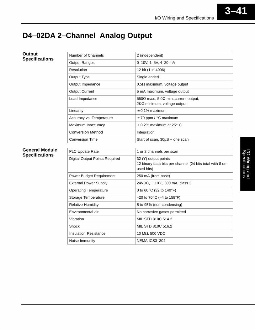
Getting S
tartedI/O
Wiring and
Specifications
3–41I/O Wiring and Specifications
D4–02DA 2–Channel Analog Output
Number of Channels 2 (independent)
Output Ranges 0–10V, 1–5V, 4–20 mA
Resolution 12 bit (1 in 4096)
Output Type Single ended
Output Impedance 0.5Ω maximum, voltage output
Output Current 5 mA maximum, voltage output
Load Impedance 550Ω max., 5.0Ω min.,current output,2KΩ minimum, voltage output
Linearity 0.1% maximum
Accuracy vs. Temperature 70 ppm / C maximum
Maximum Inaccuracy 0.2% maximum at 25 C
Conversion Method Integration
Conversion Time Start of scan, 30µS + one scan
PLC Update Rate 1 or 2 channels per scan
Digital Output Points Required 32 (Y) output points12 binary data bits per channel (24 bits total with 8 un-used bits)
Power Budget Requirement 250 mA (from base)
External Power Supply 24VDC, 10%, 300 mA, class 2
Operating Temperature 0 to 60C (32 to 140°F)
Storage Temperature –20 to 70C (–4 to 158°F)
Relative Humidity 5 to 95% (non-condensing)
Environmental air No corrosive gases permitted
Vibration MIL STD 810C 514.2
Shock MIL STD 810C 516.2
Insulation Resistance 10 M, 500 VDC
Noise Immunity NEMA ICS3–304
OutputSpecifications
General ModuleSpecifications

Get
ting
Sta
rted
I/O W
iring
and
Spe
cific
atio
ns3–42
I/O Wiring and Specifications
D4–02DA 2–Channel Analog Output Module
1248
163264
128
TB CH2
ANALOG
D4–02DA
OUTPUT
+I
–I
+V
–V
+I
–I
+V
–V
0–10VDC
DISPLAYCH
24V CH1
DATA
25651210242048
CH1
CH2
24VDC 0.3A
1–5VDC4mA–20mA
+I
–I
+V
–V
+I
–I
+V
–V
Shielded
Shielded
5 to 550 ohms
2K ohms or greater
User Load
24V
0V
See NOTE 2
Channel 1 is wired forcurrent output
Channel 2 is wired forvoltage output
NOTE 1: Shields should be connected to the 0Vterminal of the module or power supply.
NOTE 2: Unused voltage and current outputs should remain open (no connections).
OV
V+
V+
NC
CH1
CH2
D/A
D/A
See NOTE 1
+ –User
Supply
21.6 – 26.4 VDC CLASS 2D4–02DA
User Load

Getting S
tartedI/O
Wiring and
Specifications
3–43I/O Wiring and Specifications
F4–04DA 4–Channel Analog Output
Number of Channels 4
Output Ranges 0–5V, 0–10V, 5V, 10V, 4–20 mA
Resolution 12 bit (1 in 4096)
Conversion Method Successive Approximation
Output Type Single ended, 1 common
Output Impedance 0.2Ω typical, voltage output
Load Impedance 2KΩ minimum, voltage output0Ω minimum, current output
Maximum Load / Voltage 680Ω/18V, 1KΩ/24V, 1.5KΩ/36V,current output
Voltage Output Current 5 mA sink or source
Short-Circuit Current 15 mA typical, voltage output
Linearity Error 1 count (0.025%) maximum
Gain Calibration Error 8 counts maximum, voltage output–8 to +11 counts maximum, current output
Offset Calibration Error 2 counts maximum, voltage output–5 to +9 counts maximum, current output
Conversion Time 5 s maximum, settling time0.3 ms maximum, digital out to analog out
Digital Output Points Required 16 point (Y) outputs,12 bits binary data, 4 channel select bits
Power Budget Requirement 120 mA @ 5 VDC (from base)
External Power Supply 24 VDC, 100 mA, class 2 10%(add 20 mA for each current loop used)
Accuracy vs. Temperature 50 ppm / C maximum full scale25 ppm / C maximum offset
Operating Temperature 0 to 60C (32 to 140°F)
Storage Temperature –20 to 70C (–4 to 158°F)
Relative Humidity 5 to 95% (non-condensing)
Environmental air No corrosive gases permitted
Vibration MIL STD 810C 514.2
Shock MIL STD 810C 516.2
Noise Immunity NEMA ICS3-304
One count in the specification table is equal to one least significant bit of the analog data value (1 in 4096).
OutputSpecifications
General ModuleSpecifications

Get
ting
Sta
rted
I/O W
iring
and
Spe
cific
atio
ns3–44
I/O Wiring and Specifications
F4–04DA 4–Channel Analog Output Module
NOTE 1: Shields should be connected to the 0V terminal of the module or power supply.
NOTE 2: Unused voltage and current outputs should remain open (no connections).
CH1 +I
CH1
Min.2K ohms
0–1K ohms
CH1 +V
CH2 +I
CH2 +V
CH3 +I
CH3 +V
CH4 +I
CH4 +V
CH1 –I
CH1 –V
CH2 –I
CH–V
CH3 –I
CH3 –V
CH4 –I
CH4 –V
CH3
CH4
0–1K ohms
24V
0V
Voltage Output
Current
4–20mA curr. sinking
volt. sink/source4–20mA curr. sinking
volt. sink/source
volt. sink/source
volt. sink/source
D/A
Internal module circuitry
User WiringSee NOTE 1
D/A
D/A
D/A
UserSupply
21.6–26.4 VDC
TransmitterSupply
18–30 VDC
ANALOG
F4-04DA
OUTPUT
0-10VDC0-5VDC
CH1+I
CH1+V
CH2+I
CH2+V
CH3+I
CH3+V
CH4+I
CH4+V
24V0
V
4mA-20mA
24VDC 0.1A
CH1-I
CH1–V
CH2–I
CH2–V
CH3–I
CH3–V
CH4–I
CH4–V
5VD10VDC
Output
CurrentOutput
4–20mA curr. sinking
4–20mA curr. sinking
CH2
Min.2K ohms
Wiring Diagram

Getting S
tartedI/O
Wiring and
Specifications
3–45I/O Wiring and Specifications
F4–04DA–1 4–Channel Analog Current Output
Number of Channels 4, single ended (one common)
Output Range 4–20 mA
Resolution 12 bit (1 in 4095)
Output Type Outputs sink 4-20 mA from external supply
External Load Resistance 0 minimum
Maximum Loop Supply 30 VDC
Peak Output Voltage 40 VDC (clamped, transient suppressed)
Maximum Load / Power Supply 620/18V, 910/24V, 1200/30V
Linearity Error (best fit) 1 count (0.025%) maximum
Gain Calibration Error 5 counts maximum
Offset Calibration Error 3 counts maximum
Maximum Inaccuracy 0.1% @ 25C (77°F)0.3% @ 0 to 60C (32 to140°F)
Conversion Time 100 s maximum, settling time2.0 ms maximum, digital out to analog out
Digital Output Points Required 16 point (Y) outputs,12 bits binary data and 4 active channel bits
Power Budget Requirement 70 mA @ 5 VDC (from base)
External Power Supply 21.6–26.4 VDC, 75 mA, class 2(add 20 mA for each current loop used)
Accuracy vs. Temperature 57 ppm / C full scale calibration range(including maximum offset change, 2 counts)
Operating Temperature 0 to 60C (32 to 140°F)
Storage Temperature –20 to 70C (–4 to 158°F)
Relative Humidity 5 to 95% (non-condensing)
Environmental Air No corrosive gases permitted
Vibration MIL STD 810C 514.2
Shock MIL STD 810C 516.2
Noise Immunity NEMA ICS3-304
OutputSpecifications
General ModuleSpecifications

Get
ting
Sta
rted
I/O W
iring
and
Spe
cific
atio
ns3–46
I/O Wiring and Specifications
F4–04DA–1 4–Channel Analog Current Output Module
ANALOG
F4–04DA–1
OUTPUT
CH1+I
CH2+I
CH3+I
CH4+I
24V0
V
4mA–20mA
24 V @ 75 mA
CH1–I
CH2–I
CH3–I
CH4–I
NOTE 1: Shields should be connected to the 0V terminal of the module terminal block.
CH1 +ICH1
CH2 CH2 +I
CH3 +I
CH4 +I
CH1 –I
CH2 –I
CH3 –I
CH4 –I
CH3
CH4
24V
0V
18–30 VDCOptional 2ndUser Supply
Add 20mA for each4–20mA loop poweredfrom the module.
CurrentOutput
CurrentOutput
CurrentOutput
4–20mA curr. sinking
4–20mA curr. sinking
4–20mA curr. sinking
4–20mA curr. sinking
D/A
Internal module circuitry
Typical User Wiring
See NOTE 1
D/A
D/A
D/A
0–1K ohms
NOTE 2: Unused current outputs should remain open (no connections).
InternalDC/DC Converter
21.6 – 26.4 VDC75 mA
+ –User Supply
+ –
CurrentOutput
0–1K ohms
0–1K ohms
0–1K ohms
Wiring Diagram

Getting S
tartedI/O
Wiring and
Specifications
3–47I/O Wiring and Specifications
F4–04DA–2 4–Channel Analog Voltage Output
Number of Channels 4, single ended (one common)
Output Ranges 0–5, 0–10, 5 , 10 VDC
Resolution 12 bit (1 in 4095)
Load Impedance 2K minimum
Load Capacitance 0.01 uF maximum
Voltage Output Current 5.0 mA sink or source
Short-circuit Current 15 mA typical
Linearity Error (end to end)and Relative Accuracy
1 count (0.025%) maximum
Offset Calibration Error 3 counts maximum, unipolar4 counts maximum, bipolar
Full Scale Calibration Error 8 counts maximum, (offset error included)
Maximum Inaccuracy 0.2% @ 25C (77°F)0.4% @ 0 to 60 C (32 to140°F)
Conversion Time 5 s maximum, settling time2.0 ms maximum, digital out to analog out
Digital Output Points Required 16 point (Y) outputs,12 bits binary data, 4 active channel bits or 2 activechannel bits and 1 sign bit for bipolar
Power Budget Requirement 90 mA @ 5 VDC (from base)
External Power Supply 21.6–26.4 VDC, 90 mA, class 2(outputs fully loaded)
Accuracy vs. Temperature 57 ppm / C full scale calibration change(including maximum offset change, 2 counts)
Operating Temperature 0 to 60C (32 to 140°F)
Storage Temperature –20 to 70C (–4 to 158°F)
Relative Humidity 5 to 95% (non-condensing)
Environmental air No corrosive gases permitted
Vibration MIL STD 810C 514.2
Shock MIL STD 810C 516.2
Noise Immunity NEMA ICS3-304
OutputSpecifications
General ModuleSpecifications

Get
ting
Sta
rted
I/O W
iring
and
Spe
cific
atio
ns3–48
I/O Wiring and Specifications
F4–04DA–2 4–Channel Analog Voltage Output Module
ANALOG
F4–04DA–2
OUTPUT
0–10VDC0–5VDC
CH1+V
CH2+V
CH3+V
CH4+V
24V0
V
24 V @ 75 mA
CH1–V
CH2–V
CH3–V
CH4–V
NOTE 1: Shields should be connected to the 0V terminal of the module or power supply.
CH1
2K ohm min
CH2
CH1 +V
CH2 +V
CH3 +V
CH4 +V
CH1 –V
CH2 –V
CH3 –V
CH4 –V
CH3
CH4
24V
0V
21.6 – 26.4 VDC
90mA
VoltageOutput volt. sink/source
D/A
Internal module circuitryUser Wiring See NOTE 1
D/A
D/A
D/A
”10VDC”5VDC
NOTE 2: Unused voltage outputs should remain open (no connections).
InternalDC/DC
+ –
2K ohm min
2K ohm min
2K ohm min
VoltageOutput
volt. sink/source
volt. sink/source
volt. sink/source
Converter
Wiring Diagram

Getting S
tartedI/O
Wiring and
Specifications
3–49I/O Wiring and Specifications
F4–04DAS–1 4–Channel 4–20mA Isolated Analog Output
Number of Channels 4, isolated current sourcing
Output Ranges 4–20mA current
Resolution 16 bit (1 in 65536)
Output Type Outputs source 4–20 mA from external supply
Isolation Voltage 750V continuous, channel to channel, channel to logic
Load Impedance 0 – 1375
Loop Supply 12–32VDC
Output Loop Compliance Vin–2.5V
Max. Load/Power Supply 375/12V, 975/24V, 1375/32V
PLC Update Rate 1 channel per scan min.,4 per scan max.
Linearity Error (end to end)and Relative Accuracy
10 count (0.015%) maximum
Offset Calibration Error 13 counts (0.02%)
Gain Calibration Error 32 counts maximum, (offset error included)
Maximum Inaccuracy 0.07% @ 25C (77°F)0.18% @ 0 to 60 C (32 to140°F)
Conversion Time 3ms to 0.1% of full scale
Digital Output Points Required 32 point (Y) outputs,16 bits binary data, 2 channel identification bits and 1output enable
Power Budget Requirement 60 mA @ 5 VDC (from base)
External Power Supply 50 mA per channel
Accuracy vs. Temperature 50 ppm / C full scale calibration change(including maximum offset change, 2 counts)
Operating Temperature 0 to 60C (32 to 140°F)
Storage Temperature –20 to 70C (–4 to 158°F)
Relative Humidity 5 to 95% (non-condensing)
Environmental air No corrosive gases permitted
Vibration MIL STD 810C 514.2
Shock MIL STD 810C 516.2
Noise Immunity NEMA ICS3-304
OutputSpecifications
General ModuleSpecifications

Get
ting
Sta
rted
I/O W
iring
and
Spe
cific
atio
ns3–50
I/O Wiring and Specifications
F4–04DAS–1 4–Channel 4–20mA Isolated Analog OutputModule
4 CHANNELS
ANALOG
F4–04DAS–1
OUTPUT
+V1
+I1
0V2
–I2
+V3
+I3
–I4
+I4
0V4
0V1
–I1
+V2
+I2
0V3
–I3
–I
+V4
NOTE 1: Shields should be connected to the 0V.
NOTE 2: Load must be within compliance voltage.
CH1
0–1375Ω
CH2
CH3
CH4
–I4
+14
D/A
Internal module circuitry
User Wiring
D/A
D/A
D/A
+–Transmitter
Supply12–32VDC
+–Transmitter
Supply12–32VDC
0–1375 Ω
0–1375 Ω
0–1375Ω
+–Transmitter
Supply12–32VDC
+–Transmitter
Supply12–32VDC
4mA–20mA
Note 3
100Ω
100Ω
100Ω
100Ω
NOTE 3: For non–isolated outputs, connect all 0V’s together(0V1 .......0V4) and connect all +V’s together(+V1 .......+V4).
Note 2
Note 2
Note 2
Note 2
Wiring Diagram

Getting S
tartedI/O
Wiring and
Specifications
3–51I/O Wiring and Specifications
F4–08DA–1 8–Channel Analog Current Output
Number of Channels 8, single ended (one common)
Output Range 4–20 mA current
Resolution 12 bit (1 in 4095)
Output Type Outputs sink 4–20 mA from external supply
Peak Output Voltage 40 VDC (no transient voltage suppression)
External Load Resistance 0–480 at 18V, 220–740at 24V,1550–1760at 48V
Maximum Loop Supply 48 VDC (with load resistance in proper range)
Crosstalk –70 dB, 1 count maximum
Linearity Error (end-to-end) and Rela-tive Accuracy
1 count maximum
Full Scale Calibration Error(offset error included)
8 counts maximum (20mA at 25C)
Offset Calibration Error 3 counts maximum (4mA at 25C)
Maximum Inaccuracy 0.2% at 25C (77°F) 0.4% at 0 to 60C (32 to140°F)
Conversion Time 400 s maximum, for full scale change2.25 to 4.5 mS for digital output to analog out
Digital Output Points Required 16 point (Y) outputs,12 bits binary data, 3 bits channel select,1 bit output enable
Power Budget Requirement 90 mA at 5 VDC (supplied by base power supply)
External Power Supply 21.6-26.4 VDC, 100 mA, class 2(add 20 mA for each current loop used)
Accuracy vs. Temperature 57 ppm / C full scale calibration range(including maximum offset change, 2 counts)
Operating Temperature 0 to 60C (32 to 140°F)
Storage Temperature –20 to 70C (–4 to 158°F)
Relative Humidity 5 to 95% (non-condensing)
Environmental Air No corrosive gases permitted
Vibration MIIL STD 810C 514.2
Shock MIL STD 810C 516.2
Noise Immunity NEMA ICS3-304
OutputSpecifications
General ModuleSpecifications

Get
ting
Sta
rted
I/O W
iring
and
Spe
cific
atio
ns3–52
I/O Wiring and Specifications
F4–08DA–1 8–Channel Analog Current Output Module
ANALOG
F4–08DA–1
OUTPUT
CH1–I
CH5–I
+
–
4mA–20mA
24 VDC 90mA
CH2–I
CH6–I
NOTE 1: Shields should be connected to the 0V of the User
CH1
CH1
0–1K ohms
CH2
CH5
CH8
24V0V
18–48 VDCOptional
Loop Supply
Add 20mA for each4–20mA loop powered
from this supply.
Current
Output4–20mA current sinking D/A
Internal module circuitry
Typical User Wiring
See NOTE 1
0–1K ohms
0–1K ohms
NOTE 2: Unused current outputs should remain open (no connections).
InternalDC/DC
21.6 – 26.4 VDC100mA
+ –User Supply
+ –
CH3–I
CH7–I
0V
CH4–I
CH8–I
0V
D/AD/A
D/A
D/A
D/A
D/A
D/A4–20mA curr. sinking
(same)
(same)
CH3
CH7
(same)
CH2
CH6
CH4
CH8
0V
0V
Current
Output
Current
Output
Converter
Power Supply at the module terminal block.
Wiring Diagram
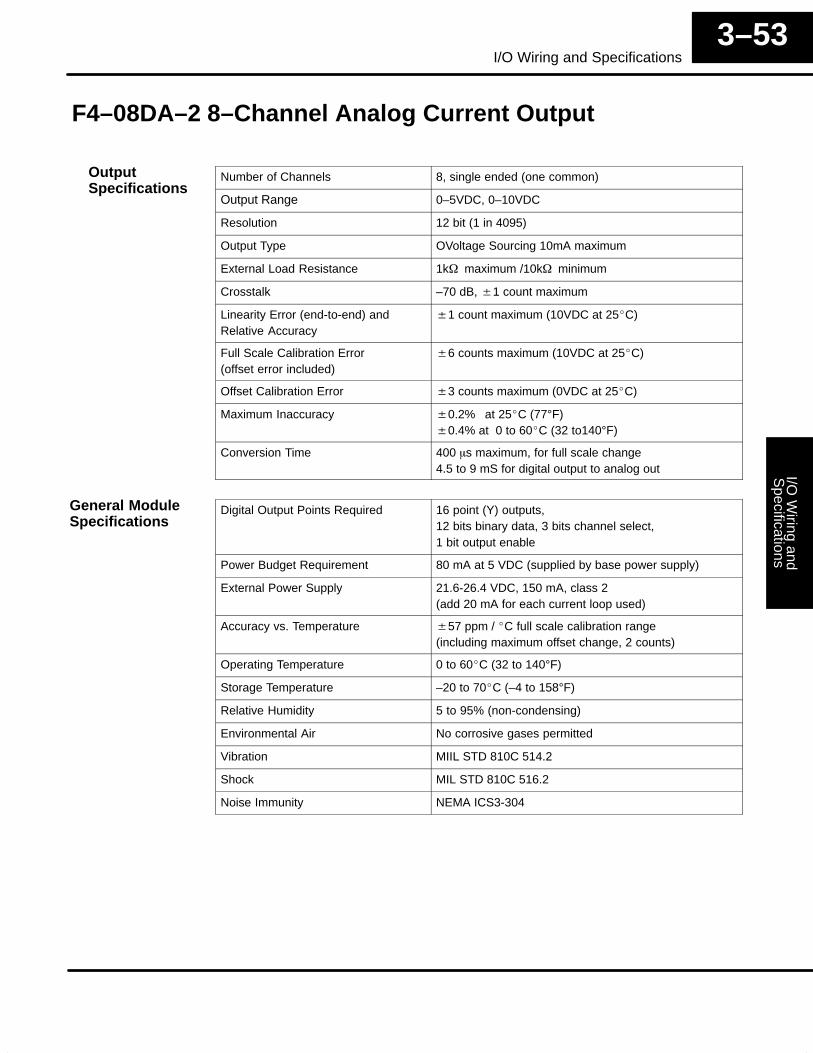
Getting S
tartedI/O
Wiring and
Specifications
3–53I/O Wiring and Specifications
F4–08DA–2 8–Channel Analog Current Output
Number of Channels 8, single ended (one common)
Output Range 0–5VDC, 0–10VDC
Resolution 12 bit (1 in 4095)
Output Type OVoltage Sourcing 10mA maximum
External Load Resistance 1k maximum /10kminimum
Crosstalk –70 dB, 1 count maximum
Linearity Error (end-to-end) andRelative Accuracy
1 count maximum (10VDC at 25C)
Full Scale Calibration Error(offset error included)
6 counts maximum (10VDC at 25C)
Offset Calibration Error 3 counts maximum (0VDC at 25C)
Maximum Inaccuracy 0.2% at 25C (77°F) 0.4% at 0 to 60C (32 to140°F)
Conversion Time 400 s maximum, for full scale change4.5 to 9 mS for digital output to analog out
Digital Output Points Required 16 point (Y) outputs,12 bits binary data, 3 bits channel select,1 bit output enable
Power Budget Requirement 80 mA at 5 VDC (supplied by base power supply)
External Power Supply 21.6-26.4 VDC, 150 mA, class 2(add 20 mA for each current loop used)
Accuracy vs. Temperature 57 ppm / C full scale calibration range(including maximum offset change, 2 counts)
Operating Temperature 0 to 60C (32 to 140°F)
Storage Temperature –20 to 70C (–4 to 158°F)
Relative Humidity 5 to 95% (non-condensing)
Environmental Air No corrosive gases permitted
Vibration MIIL STD 810C 514.2
Shock MIL STD 810C 516.2
Noise Immunity NEMA ICS3-304
OutputSpecifications
General ModuleSpecifications

Get
ting
Sta
rted
I/O W
iring
and
Spe
cific
atio
ns3–54
I/O Wiring and Specifications
F4–08DA–2 8–Channel Analog Voltage Output Module
ANALOG
F4–08DA–2
OUTPUT
CH1+V
CH5+V
+
–
0–5VDC
24 VDC 150mA
CH2+V
CH6+V
NOTE 1: Shields should be connected to the 0V terminal of the User
CH1
CH1
CH2
CH5
CH8
24V0V
Voltage
Output0–10 V Sourcing D/A
Internal module circuitry
Typical User Wiring
See NOTE 1
1k–10kΩ
InternalDC/DC
21.6 – 26.4 VDC150mA
+ –User Supply
CH3+v
CH7+V
0V
CH4+V
CH8+V
0V
D/AD/A
D/A
D/A
D/A
D/A
D/A0–10 V Sourcing
(same)
(same)
CH3
CH7
(same)
CH2
CH6
CH4
CH8
0V
0V
Voltage
Output
VoltageOutput
Converter
Power Supply at the module terminal block.
0–10VDC
1k–10kΩ
1k–10kΩ

Getting S
tartedI/O
Wiring and
Specifications
3–55I/O Wiring and Specifications
F4–16DA–1 16–Channel Analog Current Output
Number of Channels 16, single ended (one common)
Output Range 4–20 mA current
Resolution 12 bit (1 in 4095)
Output Type Outputs sink 4–20 mA from external supply
Peak Output Voltage 40 VDC (no transient voltage suppression)
External Load Resistance 0–480 @ 18V, 220–740 @ 24V,1550–1760 @ 48V
Maximum Loop Supply 48 VDC (with load resistance in proper range)
Crosstalk –70 dB, 1 count maximum
Linearity Error (end-to-end) and Rela-tive Accuracy
1 count maximum (20mA at 25C)
Full Scale Calibration Error(offset error included)
8 counts maximum (20mA at 25C)
Offset Calibration Error 3 counts maximum (4mA at 25C)
Maximum Inaccuracy 0.2% @ 25C (77°F) 0.4% @ 0 to 60C (32 to 140°F)
Conversion Time 400 s maximum, for full scale change4.5 to 9 mS for digital output to analog out
Digital Output Points Required 32 point (Y) outputs,2 sets each of 12 bits binary data, 3 bits channel select,1 bit output enable
Power Budget Requirement 90 mA @ 5 VDC (supplied by base)
External Power Supply 21.6 – 26.4 VDC, 100 mA, class 2(add 20 mA for each current loop used)
Accuracy vs. Temperature 57 ppm / C full scale calibration range(including maximum offset change, 2 counts)
Operating Temperature 0 to 60C (32 to 140°F)
Storage Temperature –20 to 70C (–4 to 158°F)
Relative Humidity 5 to 95% (non-condensing)
Environmental Air No corrosive gases permitted
Vibration MIL STD 810C 514.2
Shock MIL STD 810C 516.2
Noise Immunity NEMA ICS3-304
OutputSpecifications
General ModuleSpecifications
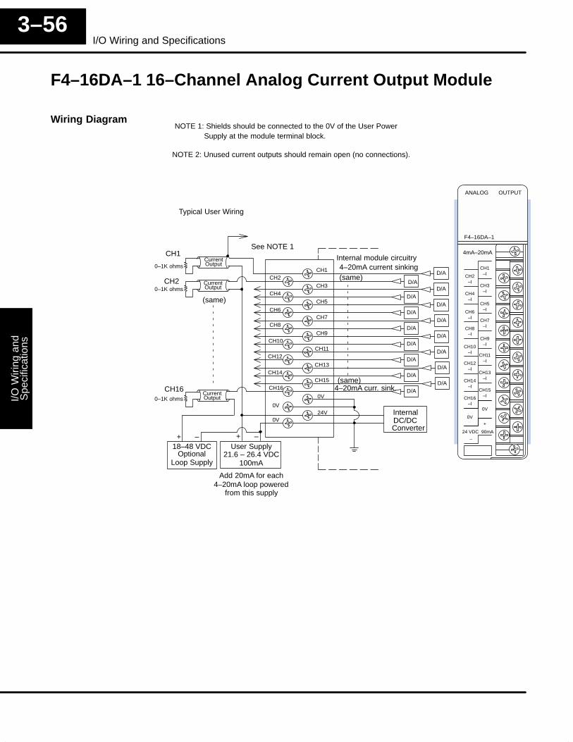
Get
ting
Sta
rted
I/O W
iring
and
Spe
cific
atio
ns3–56
I/O Wiring and Specifications
F4–16DA–1 16–Channel Analog Current Output Module
ANALOG
F4–16DA–1
OUTPUT
CH1–I
CH5–I
CH9–I
CH13–I
+
–
4mA–20mA
24 VDC 90mA
CH2–I
CH6–I
CH10–I
CH14–I
NOTE 1: Shields should be connected to the 0V of the User Power
CH1
CH1
CH2
CH5
CH9
CH13
CH16
24V0V
18–48 VDCOptional
Loop Supply
Add 20mA for each4–20mA loop powered
from this supply
CurrentOutput
4–20mA current sinkingD/A
Internal module circuitry
Typical User Wiring
See NOTE 1
0–1K ohms
NOTE 2: Unused current outputs should remain open (no connections).
InternalDC/DC
21.6 – 26.4 VDC100mA
+ –User Supply
+ –
CH3–I
CH7–I
CH11–I
CH15–I
0V
CH4–I
CH8–I
CH12–I
CH16–I
0V
D/AD/A
D/A
D/A
D/A
D/A
D/A
D/A
D/A
D/A
D/A
D/A
D/AD/A
D/A4–20mA curr. sink.
(same)
(same)
CH3
CH7
CH11
CH15
(same)
CH2
CH6
CH10
CH14
CH4
CH8
CH12
CH16
0V
0V
Supply at the module terminal block.
Converter
CurrentOutput
CurrentOutput
0–1K ohms
0–1K ohms
Wiring Diagram
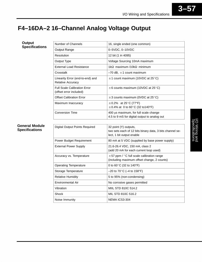
Getting S
tartedI/O
Wiring and
Specifications
3–57I/O Wiring and Specifications
F4–16DA–2 16–Channel Analog Voltage Output
Number of Channels 16, single ended (one common)
Output Range 0–5VDC, 0–10VDC
Resolution 12 bit (1 in 4095)
Output Type Voltage Sourcing 10mA maximum
External Load Resistance 1k maximum /10kminimum
Crosstalk –70 dB, 1 count maximum
Linearity Error (end-to-end) andRelative Accuracy
1 count maximum (10VDC at 25C)
Full Scale Calibration Error(offset error included)
6 counts maximum (10VDC at 25C)
Offset Calibration Error 3 counts maximum (0VDC at 25C)
Maximum Inaccuracy 0.2% at 25C (77°F) 0.4% at 0 to 60C (32 to140°F)
Conversion Time 400 s maximum, for full scale change4.5 to 9 mS for digital output to analog out
Digital Output Points Required 32 point (Y) outputs,two sets each of 12 bits binary data, 3 bits channel se-lect, 1 bit output enable
Power Budget Requirement 80 mA at 5 VDC (supplied by base power supply)
External Power Supply 21.6-26.4 VDC, 150 mA, class 2(add 20 mA for each current loop used)
Accuracy vs. Temperature 57 ppm / C full scale calibration range(including maximum offset change, 2 counts)
Operating Temperature 0 to 60C (32 to 140°F)
Storage Temperature –20 to 70C (–4 to 158°F)
Relative Humidity 5 to 95% (non-condensing)
Environmental Air No corrosive gases permitted
Vibration MIIL STD 810C 514.2
Shock MIL STD 810C 516.2
Noise Immunity NEMA ICS3-304
OutputSpecifications
General ModuleSpecifications

Get
ting
Sta
rted
I/O W
iring
and
Spe
cific
atio
ns3–58
I/O Wiring and Specifications
F4–16DA–2 16–Channel Analog Voltage Output Module
NOTE 1: Shields should be connected to the 0V terminal of the User Power
CH1
CH1
CH2
CH5
CH9
CH13
CH16
24V0V
VoltageOutput
0–10 V SourcingD/A
Internal module circuitry
Typical User Wiring
See NOTE 1
1kΩ–10kΩ
InternalDC/DC
21.6 – 26.4 VDC275mA
+ –User Supply
D/AD/A
D/A
D/A
D/A
D/A
D/A
D/A
D/A
D/A
D/A
D/A
D/AD/A
D/A0–10 V Sourcing
(same)
(same)
CH3
CH7
CH11
CH15
(same)
CH2
CH6
CH10
CH14
CH4
CH8
CH12
CH16
0V0V
Supply at the module terminal block.
Converter
VoltageOutput
VoltageOutput
1kΩ–10kΩ
1kΩ–10kΩ
ANALOG
F4–16DA–2
OUTPUT
CH1+V
CH5+V
CH9+V
CH13+V
+
–
0–5VDC
24 VDC 275mA
CH2+V
CH6+V
CH10+V
CH14+V
CH3+V
CH7+V
CH11+V
CH15+V
0V
CH4+V
CH8+V
CH12+V
CH16+V
0V
0–10VDC

Getting S
tartedI/O
Wiring and
Specifications
3–59I/O Wiring and Specifications
F4–08THM 8–Channel Thermocouple Input
Number of Channels 8, differential inputs
Input Ranges Type J: –190/760 C, –310/1400 FType E: –210/1000 C, –346/1832 FType K: –150/1372 C, –238/2502 FType R: 65/1768 C, 149/3214 FType S: 65/1768 C, 149/3214 FType T: –230/400 C, –382/752 FType B: 529/1820 C, 984/3308FType N: –70/1300 C, –94/2372FType C: –65/2320 C, –146/4208 F
Display Resolution 0.1° C or 0.1° FInput Impedance 1M
Absolute Maximum Ratings Fault-protected input, 50 VDC
Cold Junction Compensation Automatic
Conversion Time 100ms per channel, minimum
Linearity Error .05° C maximum, .01° C typical
Full Scale Calibration Error 13 counts typical, 33 counts max.
Maximum Inaccuracy* .02% @ 25° C
PLC Update Rate 8 channel per scan max.
Digital Input Points Required 16 (X) input points, including , 2 channel ID bits, 4 diagnostic bit
Power Budget Requirement 110 mA @ 5 VDC (from base)
External Power Supply 60 mA maximum, 18 to 26.4VDC
Operating Temperature 0° to 60° C (32° to 140° F)
Storage Temperature –20° to 70° C (–4° to 158° F)
Accuracy vs. Temperature 57 ppm / C maximum full scale
Relative Humidity 5 to 95% (non-condensing)
Environmental air No corrosive gases permitted
Vibration MIL STD 810C 514.2
Shock MIL STD 810C 516.2
Noise Immunity NEMA ICS3–304
InputSpecifications
GeneralSpecifications

Get
ting
Sta
rted
I/O W
iring
and
Spe
cific
atio
ns3–60
I/O Wiring and Specifications
F4–08THM 8–Channel Thermocouple Input Module
C
–1
+1
–2
+2
–3
+3
–4
+4
C
–5
+5
–6
+6
–7
+7
–8
+8
COM
24V+
CH1
CH3
CH4
CH8
Examples of groundedThermocouple wiring
Examples of differentialThermocouple wiring
AnalogSwitch
A/D
Note 1: Terminate shields at the respective signalsource.Note 2: Leave unused channels open (no connection). Internal Module Wiring
0V
CH5
+–
User Supply
24VDC+ 10% Class 2
See Note 1 8 CHANNELS
F4–08THM
COMCH1 –CH1+CH2–CH2+CH3–CH3+CH4–CH4+
CH5–CH5+CH6–CH6+CH7–CH7+CH8–CH8+COM24V0V
THERMOCOUPLE INPUT
COM
24V @40mA

Getting S
tartedI/O
Wiring and
Specifications
3–61I/O Wiring and Specifications
F4–08THM–n 8–Channel Thermocouple Input
Number of Channels 8, differential inputs
Input Ranges Type E: –270/1000 C, –450/1832 FType J: –210/760 C, –350/1390 FType K: –270/1370 C, –450/2500 FType R: 0/1768 C, 32/3214 FType S: 0/1768 C, 32/3214 FType T: –270/400 C, –450/752 FType C: 60/2320 C, 149/4208FType B: 529/1820 C, 984/3594FType P: –99/1395 C, –146/2543 F–1: 0–50 mV–2: 0–100 mV–3: 0–25 mV
Resolution 12 bit (1 in 4096)
Input Impedance 27K DC
Absolute Maximum Ratings Fault-protected input, 130 Vrms or 100 VDC
Cold Junction Compensation Automatic
Conversion Time 15ms per channel, minimum1 channel per CPU scan
Converter Type Successive approximation
Linearity Error 1 count (0.03% of full scale) maximum
Full Scale Calibration Error 0.35% of full scale
Maximum Inaccuracy* 1° C type J,K,E,T thermocouples
3° C type R,S,B,C,P thermocouples
* Maximum Inaccuracy is guaranteed for temperatures above –220°C for types E, T, J, and K, and above +100°C for types R and S.
PLC Update Rate 8 channel per scan max.
Digital Input Points Required 16 (X) input points, including 12 binary data bits, 3 chan-nel ID bits, 1 sign bit
Power Budget Requirement 120 mA @ 5 VDC (from base)
External Power Supply 24 VDC 10%, 50 mA current
Operating Temperature 0° to 60° C (32° to 140° F)
Storage Temperature –20° to 70° C (–4° to 158° F)
Accuracy vs. Temperature 57 ppm / C maximum full scale
Relative Humidity 5 to 95% (non-condensing)
Environmental air No corrosive gases permitted
Vibration MIL STD 810C 514.2
Shock MIL STD 810C 516.2
Noise Immunity NEMA ICS3–304
InputSpecifications
GeneralSpecifications

Get
ting
Sta
rted
I/O W
iring
and
Spe
cific
atio
ns3–62
I/O Wiring and Specifications
F4–08THM–n 8–Channel Thermocouple Input Module
C
–1
+1
–2
+2
–3
+3
–4
+4
C
–5
+5
–6
+6
–7
+7
–8
+8
COM
24V+
CH1
CH3
CH4
CH8
Examples of groundedThermocouple wiring
Examples of differentialThermocouple wiring
AnalogSwitch
A/D
Note 1: Terminate shields at the respective signalsource.Note 2: Leave unused channels open (no connection). Internal Module Wiring
0V
CH5
+–
User Supply
24VDC+ 10% Class 2
See Note 1
TEMPERATURE INPUT
F4–08THM
COMCH1 –CH1+CH2–CH2+CH3–CH3+CH4–CH4+
CH5–CH5+CH6–CH6+CH7–CH7+CH8–CH8+COM24V0V
THERMOCOUPLE
COM
24V @40mA

Getting S
tartedI/O
Wiring and
Specifications
3–63I/O Wiring and Specifications
F4–08RTD 8–Channel RTD Input
Number of Channels 8 differential inputs
Input Ranges Pt100 –200°C/850°C (–328°F/1562°F)
Pt 1000 –200°C/595°C (–328°F/1103°F)
jPt100 –38°C/450°C (–36°F/842°F)
10ΩCu. –200°C/260°C (–328°F/500°F)
25ΩCu. –200°C/260°C (–328°F/500°F)
Display Resolution 0.01 °C, 0.01 °F (3276.7)
Resolution 15-bit (1 in 32768)
Absolute Maximum Ratings Fault-protected input, 22 VDC
Converter Type Charge balancing, 24-bit
Sampling Rate 160 msec per channel
Temperature Drift 5ppm per °C (maximum)
Common Mode Range 0–5 VDC
Linearity Error .05° C maximum, .01° C typical
Full Scale Calibration 1° C
PLC Update Rate 8 Channels/Scan max. DL440/DL450 CPUs1 Channel/Scan max. DL430 CPU
Digital Input Points Required 32 (X) input points, 16 binary data bits, 3 channel ID bits, 8 fault bits
Power Budget Requirement 80 mA @ 5 VDC (from base)
Operating Temperature 0° to 60°C (32° to 140°F)
Storage Temperature –20° to 70°C (–4° to 158°F)
Relative Humidity 5 to 95% (non-condensing)
Environmental Air No corrosive gases permitted
Vibration MIL STD 810C 514.2
Shock MIL STD 810C 516.2
Noise Immunity NEMA ICS3–304
InputSpecifications
GeneralSpecifications

Get
ting
Sta
rted
I/O W
iring
and
Spe
cific
atio
ns3–64
I/O Wiring and Specifications
F4–08RTD 8–Channel RTD Input Module
A/D+−
Ch1 +
Ch2 +
Ch3 –
Ch4 –
Ch5 –
Ch6 –
Ch7 +
Ch8 +
Ch1 −
Ch2 −
Ch3 +
Ch4 +
Ch5 +
Ch6 +
Ch7 −
Ch8 −
CC
CC
200 µA
Current
Source
200 µA
Current
Source
Ref.
Adj.AN
ALO
G M
ULT
IPLE
XE
R
xNote 2
Note 18 CHANNELS
RTD INPUT
F4–08RTD
CH1
+
CH2
+
COM
CH3
+
CH4
+
CH5
+
CH6
+
COM
CH1
–
CH2
–
COM
CH3
–
CH4
–
CH5
–
CH6
–
COM
CH7
+CH7
–CH8
+CH8
–
F4–08RTD
RTDINPUT
Notes:1. The three wires connecting the RTD to the module must be the same type and length. Do not use the shield or drain wire for the third connection.2. If a RTD sensor has four wires, the extra plus (+) sense wire should be left unconnected as shown.