Embed Size (px)
Citation preview
14
Ion-Beam-Induced Epitaxial Recrystallization Method and Its Recent Applications
Rossano Lang1,4, Alan de Menezes1, Adenilson dos Santos2, Shay Reboh3,4, Eliermes Meneses1, Livio Amaral4 and Lisandro Cardoso1
1Instituto de Física Gleb Wataghin - UNICAMP, Campinas, SP 2CCSST, Universidade Federal do Maranhão, Imperatriz, MA
3Groupe nMat, CEMES-CNRS, Toulouse 4Instituto de Física - UFRGS, Porto Alegre, RS
1,2,4Brazil 3France
1. Introduction
The transition from amorphous Silicon to crystalline Silicon is a process of great technological importance and has raised an enormous interest also from a purely scientific perspective. Ion irradiation through an amorphous/crystalline interface may stimulate recrystallization or layer-by-layer amorphization depending on the sample temperature and ion beam parameters. In this chapter, we address some key features of this recrystallization phenomenon. The recrystallization/amorphization process will be discussed in relation to its dependence on the energy deposited during the ion beam irradiation, the sample temperature, and the presence of impurities, such as iron atoms dissolved within an amorphous silicon layer. Also it will be discussed the specific experimental condition under which a metastable phase of the FeSi2 binary compound is trapped within a region of the recrystallized Silicon, in the form of nanoparticles. Theses nanoparticles, with different orientations and morphologies, are shown to cause interesting distortions in the surrounding Si crystal lattice. This effect reflects an important application of the ion-beam induced recrystallization process, as a method that could be used to synthesize ordered nanoparticles within a Silicon matrix.
2. Epitaxial crystallization
The amorphous Silicon (a-Si) is a Si phase with well-defined thermodynamic properties and that presents Gibbs free energy of ~ 0.12 eV/at. higher than that of the crystalline phase (c-Si) (Donovan et al., 1985, 1989; Roorda et al., 1989). This implies the existence of a driving force for the transition from the amorphous to the crystalline phase to occur. In other words, there is a natural tendency for the (a-Si) → (c-Si) transformation. At room temperature, the a-Si phase is metastable and it is transformed into c-Si only when submitted to high temperatures, typically higher than 450 °C (Olson & Roth, 1988; Williams, 1983). For the case of an amorphized layer on top of a Si single-crystal substrate,
www.intechopen.com
Recrystallization
352
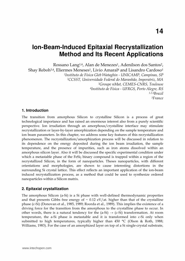
the transition occurs by a planar motion of the crystal-amorphous (c-a) interface, from the interior towards the surface, and hence decreasing the thickness of the existing amorphous layer with time, as schematically illustrated in Fig. 1. This effect is called epitaxial crystallization. For a pure thermal recrystallization process - SPEG (Solid Phase Epitaxial Growth), the growth rate is strongly dependent on the temperature and it presents an Arrhenius-like behavior with a unique activation energy of (2.68 0.05) eV over a growth rate range of more than six orders of magnitude (Olson & Roth, 1988). For instance, at 470 °C the c-a interface displacement velocity is ~ 1 Å/min while at lower temperatures, this value decreases considerably and the amorphous to crystal transition becomes kinetically inhibited. However, epitaxial recrystallization of a-Si layers can also be achieved at lower temperatures (~ 200 - 320 °C) by ion-beam irradiation. This phenomenon represents a typical example of a dynamic annealing process and it is usually referred to as Ion-Beam-Induced Epitaxial Crystallization - IBIEC (Priolo & Rimini, 1990).
It is well known that both the implantation and the irradiation processes (depending on the dose and the beam ion mass) have the amorphization of the host matrix, as one of their main effects. For the specific case of Si, when the deposited energy (energy loss of ion beam mainly by nuclear collisions) handed by the projectile exceeds the threshold value of ~ 13 eV/at. a buried amorphous Si layer is formed (Narayan et al., 1984). However, if the Si is irradiated at a temperature above ~ 150 °C, there is a competition between both phenomena: amorphization and recrystallization.
Fig. 1. Schematic illustration of two recrystallization processes in Silicon. SPEG (Solid Phase Epitaxial Growth) is a purely thermal process while, IBIEC is an ion beam induced epitaxial recrystallization process.
In fact, the temperature rise of the Si substrate is not solely responsible for this trend of the crystalline order recovery, since the recrystallization rate is greater than that obtained by a purely thermal process at the same temperature. A more complex mechanism involving a dynamic reordering stimulated by the ion beam is responsible for this effect. The recrystallization under ion-beam irradiation is the result of the prevalence of dynamic annealing over defect generation rate. Both processes depend on the substrate temperature and on the parameters of the irradiating beam, such as ion species, energy, ion dose and ion flux - also known as dose rate.
www.intechopen.com
Ion-Beam-Induced Epitaxial Recrystallization Method and Its Recent Applications
353
2.1 Crystal-amorphous interface displacement velocity
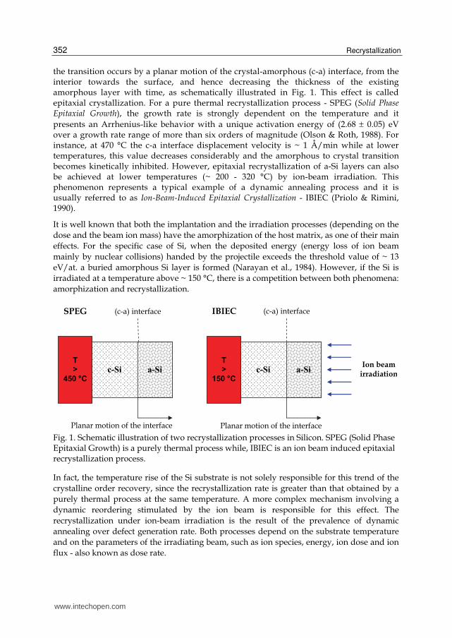
Rutherford backscattering spectrometry in combination with the ion channeling technique (RBS/C) is commonly used to directly monitor the c-a interface motion and infer the kinetics of the IBIEC process. The following RBS/C results were carried out with He+ beam at 1 MeV in a 170° scattering geometry. Figure 2 presents c-a interface position measurements of [100] oriented Si substrate previously implanted at room temperature with Fe+ ions at 100 keV energy. Channeled implantation was avoided by tilting the sample 7° normal with respect to the incident beam direction. Subsequently, the recrystallization of the Fe-implanted surface amorphous Si layer (filled circles in the figure) was induced by Si+ irradiation at high energy - 600 keV (whose projected range is well beyond the original c-a interface). In the IBIEC experiments the substrate temperature was fixed and controlled. This allows discrimination between the effects due to the heating of the sample holder and those due to ion-beam irradiation. In order to avoid beam heating effects low current density ( 1 μA/cm2) was therefore used with ion flux of ~ 6.2x10¹² ions/cm2s. The substrate temperature was maintained at 350 °C. Essentially, one observes that the increase of the Si+ irradiated dose, leads to a decrease in the distance between the c-a interface and the surface. That is, there is a recrystallization towards the surface.
Fig. 2. Determination of the thickness of an amorphous layer using the ion channeling technique. This particular case corresponds to the recrystallization of ~ 176 nm a-Si under 600 keV Si+ beam irradiation keeping the substrate at 350 °C.
In implantation processes (Dearnaley et al., 1973), the implanted dose Φ is the integral of the ion flux in time, which corresponds to the total number of ions that were focused on the sample per unit area
220
ΦΦ (ion/cm ) ; (s)A / cm
T e
e
nqIdt T
nq
, (1)
www.intechopen.com
Recrystallization
354
where: I is the beam current in ampere per unit area of the sample (A/cm2), qe is the electron charge, n = 1 for once ionized ions, n = 2 for doubly ionized species, and so on. The term I/qe is designated as the ion flux (ion/cm2s) and T(s) is the implantation time in seconds. For the IBIEC, one designates a certain irradiation dose Φ and, consequently, the ion flux for such irradiation by = dΦ/dt. When the ion flux is kept constant at a given crystallization procedure, the irradiation dose may be interpreted as a measure of the processing time described by
d Φ
d Φ Φc a c a c aX dX dXd
t d dt d . (2)
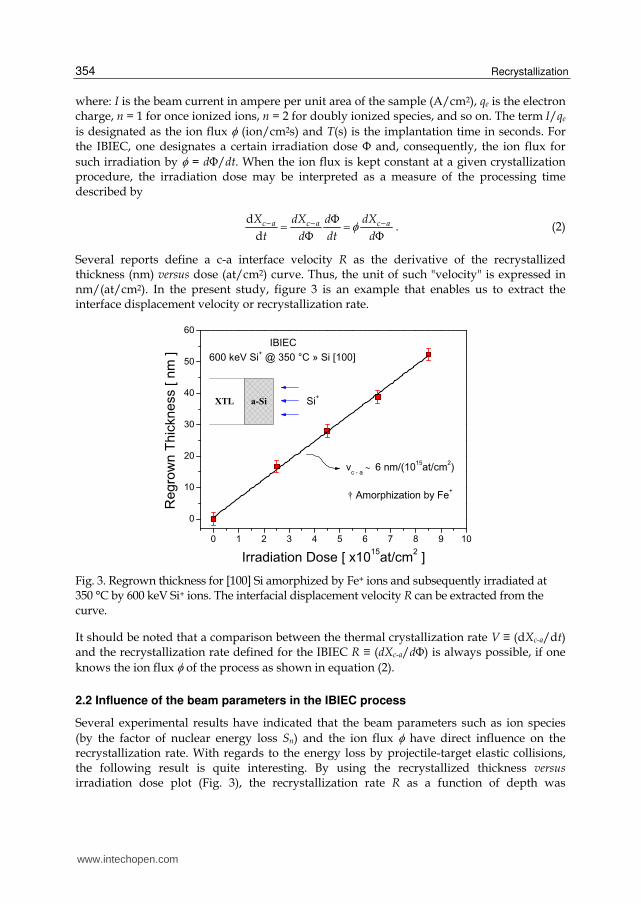
Several reports define a c-a interface velocity R as the derivative of the recrystallized thickness (nm) versus dose (at/cm2) curve. Thus, the unit of such "velocity" is expressed in nm/(at/cm2). In the present study, figure 3 is an example that enables us to extract the interface displacement velocity or recrystallization rate.
Fig. 3. Regrown thickness for [100] Si amorphized by Fe+ ions and subsequently irradiated at 350 °C by 600 keV Si+ ions. The interfacial displacement velocity R can be extracted from the curve.
It should be noted that a comparison between the thermal crystallization rate V ≡ (dXc-a/dt) and the recrystallization rate defined for the IBIEC R ≡ (dXc-a/dΦ) is always possible, if one knows the ion flux of the process as shown in equation (2).
2.2 Influence of the beam parameters in the IBIEC process
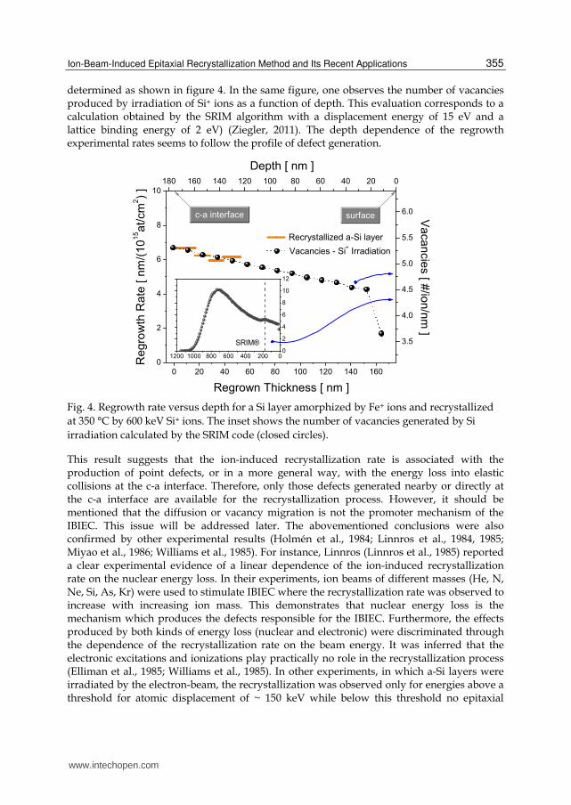
Several experimental results have indicated that the beam parameters such as ion species (by the factor of nuclear energy loss Sn) and the ion flux have direct influence on the recrystallization rate. With regards to the energy loss by projectile-target elastic collisions, the following result is quite interesting. By using the recrystallized thickness versus irradiation dose plot (Fig. 3), the recrystallization rate R as a function of depth was
www.intechopen.com
Ion-Beam-Induced Epitaxial Recrystallization Method and Its Recent Applications
355
determined as shown in figure 4. In the same figure, one observes the number of vacancies produced by irradiation of Si+ ions as a function of depth. This evaluation corresponds to a calculation obtained by the SRIM algorithm with a displacement energy of 15 eV and a lattice binding energy of 2 eV) (Ziegler, 2011). The depth dependence of the regrowth experimental rates seems to follow the profile of defect generation.
Fig. 4. Regrowth rate versus depth for a Si layer amorphized by Fe+ ions and recrystallized at 350 °C by 600 keV Si+ ions. The inset shows the number of vacancies generated by Si irradiation calculated by the SRIM code (closed circles).
This result suggests that the ion-induced recrystallization rate is associated with the production of point defects, or in a more general way, with the energy loss into elastic collisions at the c-a interface. Therefore, only those defects generated nearby or directly at the c-a interface are available for the recrystallization process. However, it should be mentioned that the diffusion or vacancy migration is not the promoter mechanism of the IBIEC. This issue will be addressed later. The abovementioned conclusions were also confirmed by other experimental results (Holmén et al., 1984; Linnros et al., 1984, 1985; Miyao et al., 1986; Williams et al., 1985). For instance, Linnros (Linnros et al., 1985) reported a clear experimental evidence of a linear dependence of the ion-induced recrystallization rate on the nuclear energy loss. In their experiments, ion beams of different masses (He, N, Ne, Si, As, Kr) were used to stimulate IBIEC where the recrystallization rate was observed to increase with increasing ion mass. This demonstrates that nuclear energy loss is the mechanism which produces the defects responsible for the IBIEC. Furthermore, the effects produced by both kinds of energy loss (nuclear and electronic) were discriminated through the dependence of the recrystallization rate on the beam energy. It was inferred that the electronic excitations and ionizations play practically no role in the recrystallization process (Elliman et al., 1985; Williams et al., 1985). In other experiments, in which a-Si layers were irradiated by the electron-beam, the recrystallization was observed only for energies above a threshold for atomic displacement of ~ 150 keV while below this threshold no epitaxial
www.intechopen.com
Recrystallization
356
regrowth was produced, even after irradiation at very high electron doses (Lulli et al., 1987; Miyao et al., 1986; Washburn et al., 1983). Therefore, the observed epitaxy is associated with elastic collisions that transfer sufficient momentum to displace target atoms from their lattice site.
As mentioned earlier in this section, there is another parameter that directly influences the process - the ion flux. In general, it is observed that the lower the flux , the higher is the effective velocity R ≡ (dXc-a/dΦ) defined by equation 2. This parameter is so important that high fluxes almost inhibit the process, especially for heavier ions (Linnros et al., 1985).
2.3 Temperature dependence
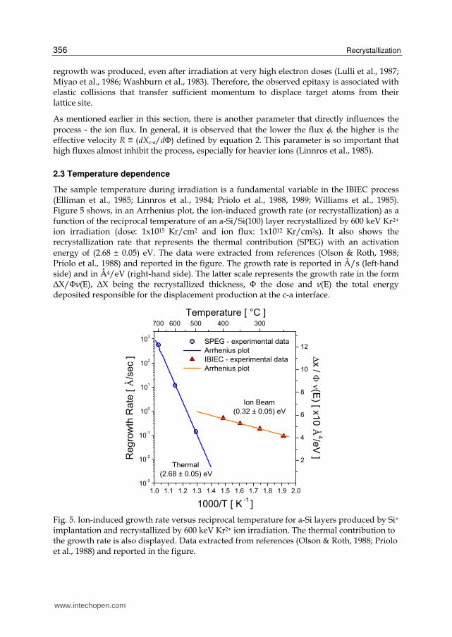
The sample temperature during irradiation is a fundamental variable in the IBIEC process (Elliman et al., 1985; Linnros et al., 1984; Priolo et al., 1988, 1989; Williams et al., 1985). Figure 5 shows, in an Arrhenius plot, the ion-induced growth rate (or recrystallization) as a function of the reciprocal temperature of an a-Si/Si(100) layer recrystallized by 600 keV Kr2+ ion irradiation (dose: 1x10¹⁵ Kr/cm2 and ion flux: 1x10¹² Kr/cm2s). It also shows the recrystallization rate that represents the thermal contribution (SPEG) with an activation energy of (2.68 0.05) eV. The data were extracted from references (Olson & Roth, 1988; Priolo et al., 1988) and reported in the figure. The growth rate is reported in Å/s (left-hand side) and in Å4/eV (right-hand side). The latter scale represents the growth rate in the form ΔX/Φν(E), ΔX being the recrystallized thickness, Φ the dose and ν(E) the total energy deposited responsible for the displacement production at the c-a interface.
Fig. 5. Ion-induced growth rate versus reciprocal temperature for a-Si layers produced by Si+ implantation and recrystallized by 600 keV Kr2+ ion irradiation. The thermal contribution to the growth rate is also displayed. Data extracted from references (Olson & Roth, 1988; Priolo et al., 1988) and reported in the figure.
www.intechopen.com
Ion-Beam-Induced Epitaxial Recrystallization Method and Its Recent Applications
357
It should be noted that recrystallization due to ion-beam irradiation occurs in a temperature range for which the thermal process is kinetically inhibited. Therefore, ion-beam irradiation strongly enhances the kinetics of recrystallization. For instance, at 250 °C the ion-induced growth rate is 0.07 Å/s while, an extrapolation of the thermal data gives a rate of only 10-10 Å/s. Furthermore, in the temperature range shown, the IBIEC presents an Arrhenius-like temperature dependence with an apparent activation energy of (0.32 0.05) eV as also demonstrated by several other experiments (Elliman et al., 1985; Linnros et al., 1984; Williams et al., 1985).
It has been proposed that the activation energy for thermal recrystallization of a-Si layers is composed of two terms: one for defect generation and other for defect migration. Ion-beam irradiation clearly removes the main activated process usually limiting conventional thermal regrowth. In fact, during ion-beam irradiation defects are not thermally generated but rather being produced by means of atomic collisions. Jackson (Jackson, 1988) proposed that the activation energy inferred from the IBIEC is not associated with any activated process and therefore considered just as an apparent activation energy. The linear dependence of the regrowth rate as a function of reciprocal temperature, in a logarithmic plot, comes instead, from a balance between different effects. In addition, Jackson (Jackson, 1988) in his intracascade model suggested the dangling bond in the amorphous phase as the promoter for IBIEC. Dangling bonds are structural defects which by moving nearby the c-a interfacial region should produce a rearrangement of the bonds leading to recrystallization. In the mid-1990s, Priolo (Priolo et al., 1990) proposed a phenomenological model of IBIEC which combines the approach of the Jackson model (Jackson, 1988) with the structural and electronic features of models proposed for conventional thermal regrowth (Williams & Elliman, 1986). This model has explained all the experimental results so far.
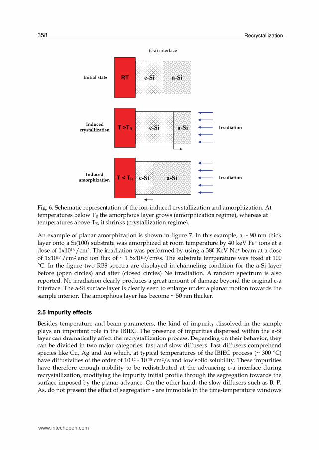
2.4 Planar amorphization
In the previous sections, it was shown how a combination of thermal energy and energy deposited by ballistic effects can produce a non-equilibrium epitaxial recrystallization. However, IBIEC is a reversible process, where the increase in the ion flux of the irradiating beam, and /or the decrease in the target temperature can cause a planar layer-by-layer amorphization instead of an epitaxial recrystallization (Elliman et al., 1987; Linnros et al., 1986, 1988). Both processes are schematically illustrated in figure 6. At a constant flux, there is a substrate temperature TR (reversal temperature) such that, when T > TR, the ion irradiation produces epitaxial regrowth whereas, when T < TR the irradiation produces a layer-by-layer amorphization. The remarkable point is that the amorphization occurs just from the pre-existing amorphous seed and not from regions below the c-a interface, despite the fact that the energy loss by elastic collisions increases with the increasing depth. In this context, the net velocity of the interface motion can be described by two terms: a crystallization and an amorphization, as
d d d
/ /Φ d d dc a c a c adX X X X
Rd t t t
. (3)
When R is positive, the crystallization regime is prevalent and when R is negative the system is in the amorphization regime.
www.intechopen.com
Recrystallization
358
Fig. 6. Schematic representation of the ion-induced crystallization and amorphization. At temperatures below TR the amorphous layer grows (amorphization regime), whereas at temperatures above TR, it shrinks (crystallization regime).
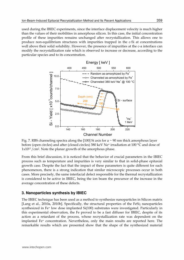
An example of planar amorphization is shown in figure 7. In this example, a ~ 90 nm thick layer onto a Si(100) substrate was amorphized at room temperature by 40 keV Fe+ ions at a dose of 1x10¹⁶ /cm2. The irradiation was performed by using a 380 KeV Ne+ beam at a dose of 1x10¹⁷ /cm2 and ion flux of ~ 1.5x10¹³/cm2s. The substrate temperature was fixed at 100 °C. In the figure two RBS spectra are displayed in channeling condition for the a-Si layer before (open circles) and after (closed circles) Ne irradiation. A random spectrum is also reported. Ne irradiation clearly produces a great amount of damage beyond the original c-a interface. The a-Si surface layer is clearly seen to enlarge under a planar motion towards the sample interior. The amorphous layer has become ~ 50 nm thicker.
2.5 Impurity effects
Besides temperature and beam parameters, the kind of impurity dissolved in the sample plays an important role in the IBIEC. The presence of impurities dispersed within the a-Si layer can dramatically affect the recrystallization process. Depending on their behavior, they can be divided in two major categories: fast and slow diffusers. Fast diffusers comprehend species like Cu, Ag and Au which, at typical temperatures of the IBIEC process (~ 300 °C) have diffusivities of the order of 10-12 - 10-15 cm2/s and low solid solubility. These impurities have therefore enough mobility to be redistributed at the advancing c-a interface during recrystallization, modifying the impurity initial profile through the segregation towards the surface imposed by the planar advance. On the other hand, the slow diffusers such as B, P, As, do not present the effect of segregation - are immobile in the time-temperature windows
www.intechopen.com
Ion-Beam-Induced Epitaxial Recrystallization Method and Its Recent Applications
359
used during the IBIEC experiments, since the interface displacement velocity is much higher than the values of their mobilities in amorphous silicon. In this case, the initial concentration profile of these impurities remains unchanged after recrystallization. This allows one to produce non-equilibrium structures with impurities trapped in the c-Si at concentrations well above their solid solubility. However, the presence of impurities at the c-a interface can modify the recrystallization rate which is observed to increase or decrease, according to the particular species and to its concentration.
Fig. 7. RBS channeling spectra along the [100] Si axis for a ~ 90 nm thick amorphous layer before (open circles) and after (closed circles) 380 keV Ne+ irradiation at 100 °C and dose of 1x10¹⁷ /cm2. Note the planar growth of the amorphous phase.
From this brief discussion, it is noticed that the behavior of crucial parameters in the IBIEC process such as temperature and impurities is very similar to that in solid-phase epitaxial growth case. Despite the fact that the impact of these parameters is quite different for each phenomenon, there is a strong indication that similar microscopic processes occur in both cases. More precisely, the same interfacial defect responsible for the thermal recrystallization is considered to be active in IBIEC, being the ion beam the precursor of the increase in the average concentration of these defects.
3. Nanoparticles synthesis by IBIEC
The IBIEC technique has been used as a method to synthesize nanoparticles in Silicon matrix [Lang et al., 2010a, 2010b]. Specifically, the structural properties of the FeSi2 nanoparticles synthesized in Fe+ low dose implanted Si(100) substrates were investigated. Particularly in this experimental observation, the Fe proved to be a fast diffuser for IBIEC, despite of its action as a retardant of the process, whose recrystallization rate was dependent on the implanted Fe+ concentration. Nevertheless, only the main results are reported here. The remarkable results which are presented show that the shape of the synthesized material
www.intechopen.com
Recrystallization
360
(observed by high resolution transmission electron microscopy - HRTEM) singularly affects the surrounding Si lattice. The lattice strain shape-dependent distribution in both directions: out-of-plane and in-plane was tailored by X-ray Bragg-Surface Diffraction technique.
3.1 Fe+ ion implantation in Si(100) and recrystallization process
A Si(100) n-type Czochralski wafer (thickness 500 μm, resistivity 10 - 20 Ω cm) was used as host matrix. Fe+ ions at 40 keV were implanted at room temperature at an ion dose of 5x1015 cm-2. Channeling effects were avoided by tilting the sample 7º normal with respect to the incident beam direction. The typical iron beam current density during implantation was about 150 nA/cm2. Subsequently, ion-beam recrystallization experiments were performed at 350 °C using a 600 keV Si+ beam (current density 1 μA/cm2) to a total dose of 6x10¹⁶ ions/cm2. The dose rate resulting from the Si beam current was 6.2x10¹² ions/cm2s. It is worth noting that Si+ ions at 600 keV energy have a projected range (average depth) of ~ 770 nm with a straggle (standard deviation) of ~ 150 nm. These values ensure that the irradiation exceeds the pre-existing amorphous layer (well beyond the original c-a interface).
The structures obtained into the as-implanted and recrystallized samples were analyzed and characterized by Rutherford Backscattering Spectrometry combined with ion channeling technique (RBS/C - with He+ beam at 1 MeV in a 170° scattering geometry) and also by transmission electron microscopy (TEM - JEOL 2010 operating at 200 kV). High-resolution rocking curves, as well as the reflection mappings of the Bragg-Surface Diffraction reflections, i.e., at the exact multiple diffraction condition, were carried out using the Huber multiaxis diffractometer of the XRD1 beam-line (Brazilian Synchrotron Radiation Facility - LNLS), with an incident beam wavelength of = 1.5495(5) Å, as defined by using a Si(111) channel-cut monochromator.
3.1.1 RBS and TEM – Results and discussion
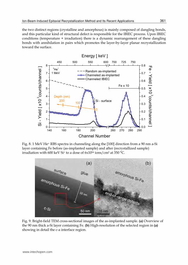
Figure 8 shows RBS/C spectra obtained at random and [100]-channeled direction from the samples before (as-implanted) and after (recrystallized) irradiation. As observed in the aligned as-implanted spectrum, the implantation has produced an amorphous layer over ~ 90 nm while no channeling in the Fe signal was observed. However, expressive reduction of dechanneling yield in the Si profile is detected after IBIEC process (aligned IBIEC spectra relative to aligned as-implanted spectra). This decrease reflects the crystalline order recovery. The entire amorphous Si layer was recrystallized (at an average rate of ~ 0.04 nm/s) with a minimum backscattering yield on the subsurface region being χmin ≈ 6.3 %. The RBS concentration-depth profile (not shown here) has indicated an implanted Fe peak concentration of ~ 2.8 at.% at 40 nm from the surface. However, the recrystallization process caused a slight narrowing of the Fe peak and a small segregation towards the surface. A significant degree of channeling (χFe ≈ 46 %) was also observed in the Fe spectrum.
Figure 9 shows bright-field TEM cross-section images (taken at [110]Si zone axis) of the as-implanted sample. One clearly observes (Fig. 9a) the amorphous Si layer of ~ 90 nm produced by 40 keV Fe+ implantation and the crystal-amorphous interface. Figure 9b shows in detail the c-a interface, where one can note a large amount of defects called "end-of-range defects" generated by the implantation process. This defective intermediate zone between
www.intechopen.com
Ion-Beam-Induced Epitaxial Recrystallization Method and Its Recent Applications
361
the two distinct regions (crystalline and amorphous) is mainly composed of dangling bonds, and this particular kind of structural defect is responsible for the IBIEC process. Upon IBIEC conditions (temperature + irradiation) there is a dynamic rearrangement of these dangling bonds with annihilation in pairs which promotes the layer-by-layer planar recrystallization toward the surface.
Fig. 8. 1 MeV He+ RBS spectra in channeling along the [100] direction from a 90 nm a-Si layer containing Fe before (as-implanted sample) and after (recrystallized sample) irradiation with 600 keV Si+ to a dose of 6x10¹⁶ ions/cm2 at 350 °C.
Fig. 9. Bright-field TEM cross-sectional images of the as-implanted sample. (a) Overview of the 90 nm thick a-Si layer containing Fe. (b) High-resolution of the selected region in (a) showing in detail the c-a interface region.
www.intechopen.com
Recrystallization
362
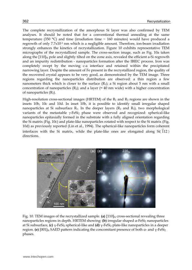
The complete recrystallization of the amorphous Si layer was also confirmed by TEM analyses. It should be noted that for a conventional thermal annealing at the same temperature (350 °C) and time (irradiation time ~ 160 minutes) would have produced a regrowth of only 7.7x10⁻³ nm which is a negligible amount. Therefore, ion-beam irradiation strongly enhances the kinetics of recrystallization. Figure 10 exhibits representative TEM micrographs of the recrystallized sample. The cross-section image, such as Fig. 10a taken along the [110]Si pole and slightly tilted on the zone axis, revealed the efficient a-Si regrowth and an impurity redistribution - nanoparticles formation after the IBIEC process. Iron was completely swept by the moving c-a interface and retained within the precipitated narrowing layer. Despite the amount of Fe present in the recrystallized region, the quality of the recovered crystal appears to be very good, as demonstrated by the TEM image. Three regions regarding the nanoparticles distribution are observed: a thin region a few nanometers thick which is closer to the surface (R1); a Si region about 5 nm with a small concentration of nanoparticles (R2); and a layer (≈ 40 nm wide) with a higher concentration of nanoparticles (R3).
High-resolution cross-sectional images (HRTEM) of the R1 and R3 regions are shown in the insets 10b, 10c and 10d. In inset 10b, it is possible to identify small irregular shaped nanoparticles at Si subsurface R1. In the deeper layers (R2 and R3), two morphological variants of the metastable -FeSi2 phase were observed and recognized: spherical-like nanoparticles epitaxially formed in the substrate with a fully aligned orientation regarding the Si matrix (Fig. 10c) and plate-like nanoparticles rotated with respect to the Si matrix (Fig. 10d) as previously reported (Lin et al., 1994). The spherical-like nanoparticles form coherent interfaces with the Si matrix, while the plate-like ones are elongated along Si 112 directions.
Fig. 10. TEM images of the recrystallized sample. (a) [110]Si cross-sectional revealing three nanoparticles regions in depth. HRTEM showing: (b) irregular shaped ┙-FeSi2 nanoparticles at Si subsurface, (c) ┛-FeSi2 spherical-like and (d) ┛-FeSi2 plate-like nanoparticles in a deeper region. (e) [001]Si SAED pattern indicating the concomitant presence of both ┙- and ┛-FeSi2 phases.
www.intechopen.com
Ion-Beam-Induced Epitaxial Recrystallization Method and Its Recent Applications
363
Selected-area electron diffraction (SAED) pattern obtained from a plan-view specimen is presented in figure 10e. In addition to strong Bragg reflections of Si, extra spots due to the nanoparticles are apparent in the diffraction pattern. The extra spots show symmetric net patterns suggesting that there is a certain orientation relationship between the nanoparticles and the substrate lattice. From the analysis of the extra spots symmetry and lattice spacing, the diffraction pattern of Figure 10e can be explained as the overlap of cubic -FeSi2 and tetragonal ┙-FeSi2 phases. The reflections are consistent with ┙1[112] , ┙2[11 2] (straight lines) and [100]┛ (dotted line) net patterns (Behar et al., 1996; Vouroutzis et al., 2008). As the SAED measurements have identified two crystalline phases, the near-surface precipitated layer should contain ┙-FeSi2 nanoparticles.
3.2 X-ray multiple diffraction
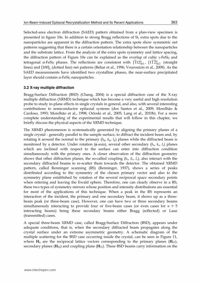
Bragg-Surface Diffraction (BSD) (Chang, 2004) is a special diffraction case of the X-ray multiple diffraction (XRMD) technique which has become a very useful and high resolution probe to study in-plane effects in single crystals in general, and also, with several interesting contributions to semiconductor epitaxial systems (dos Santos et al., 2009; Morelhão & Cardoso, 1993; Morelhão et al., 1998; Orloski et al., 2005; Lang et al., 2010b). For a more complete understanding of the experimental results that will follow in this chapter, we briefly discuss the physical aspects of the XRMD technique.
The XRMD phenomenon is systematically generated by aligning the primary planes of a single crystal - generally parallel to the sample surface, to diffract the incident beam and, by rotating it around the normal to the primary (hp, kp, lp) planes while the diffracted beam is monitored by a detector. Under rotation (-axis), several other secondary (hs, ks, ls) planes which are inclined with respect to the surface can enter into diffraction condition simultaneously with the primary ones. A closer observation of the diffraction geometry shows that other diffraction planes, the so-called coupling (hc, kc, lc), also interact with the secondary diffracted beams to re-scatter them towards the detector. The obtained XRMD pattern, called Renninger scanning (RS) (Renninger, 1937), shows a series of peaks distributed according to the symmetry of the chosen primary vector and also to the symmetry plane established by rotation of the several reciprocal space secondary points when entering and leaving the Ewald sphere. Therefore, one can clearly observe in a RS, these two types of symmetry mirrors whose position and intensity distributions are essential for most of the applications of this technique. When a peak in the RS represents an interaction of the incident, the primary and one secondary beam, it shows up as a three-beam peak (or three-beam case). However, one can have two or three secondary beams simultaneously interacting to provide four or five-beam cases (or even cases for n > 5 interacting beams) being these secondary beams either Bragg (reflected) or Laue (transmitted) cases.
A special three-beam XRMD case, called Bragg-Surface Diffraction (BSD), appears under adequate conditions, that is, when the secondary diffracted beam propagates along the crystal surface under an extreme asymmetric geometry. A schematic diagram of the multiple scattering for the BSD case occurring inside the crystal, can be seen in Figure 11, where Hij are the reciprocal lattice vectors corresponding to the primary planes (H01), secondary planes (H02) and coupling plane (H21). These BSD beams carry information on the
www.intechopen.com
Recrystallization
364
sample surface which are useful for studying surface impurity incorporation effects (Lai et al., 2005), or even on the interface (layer/substrate), if such an interface is present, as in the semiconductor epitaxial structures. The technique has provided significant information when successfully applied as a special high-resolution 3D probe for the study of epitaxial layered heterostructures. Here, the layer and substrate lattices may be separately studied just by selecting one adequate layer or substrate peak. The technique is also a method capable of measuring strain fields at the interfaces in epilayer/substrate systems with depth penetration of 2 Å resolution and with enough sensitivity to detect lattices distortions in the range of 72 Å around the epilayer/substrate interface (Sun et al., 2006).
Fig. 11. BSD scheme using its consecutive scattering model with H01 (primary), H02
(secondary) and H21 (coupling) vectors. The coupling planes re-scatter the secondary beam towards the primary direction.
Besides the standard RS, another XRMD scanning methodology can give information on the crystalline quality obtained from an analysis of the ω: mapping scans (Morelhão & Cardoso, 1996). By using this method, the rotation is performed for a range of angles each targeting an exact angular position of the multiple-beam Bragg condition. This approach results in a three dimensional plot of the primary intensity versus and in a coupled way from which, through analysis of the iso-intensity contours of such plots, one can obtain information on the lattice coherence along the beam path and hence, on the crystalline quality. It has been shown that when the FWHM (full width at half maximum) of the peak in the scan is larger in comparison to the one in the scan, there is almost no loss of coherence, i.e. confirming that the crystal is perfect or nearly perfect.
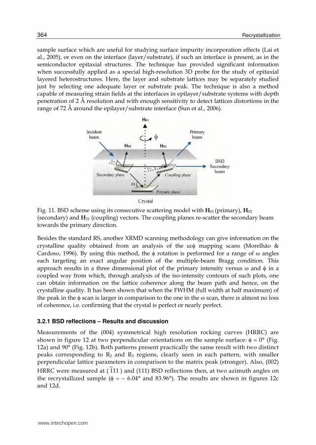
3.2.1 BSD reflections – Results and discussion
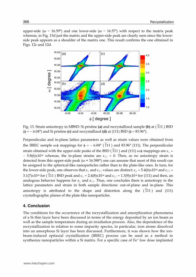
Measurements of the (004) symmetrical high resolution rocking curves (HRRC) are shown in figure 12 at two perpendicular orientations on the sample surface: 0° (Fig. 12a) and 90° (Fig. 12b). Both patterns present practically the same result with two distinct peaks corresponding to R2 and R3 regions, clearly seen in each pattern, with smaller perpendicular lattice parameters in comparison to the matrix peak (stronger). Also, (002) HRRC were measured at ( 111 ) and (111) BSD reflections then, at two azimuth angles on the recrystallized sample ( 6.04° and 83.96°). The results are shown in figures 12c and 12d.
www.intechopen.com
Ion-Beam-Induced Epitaxial Recrystallization Method and Its Recent Applications
365
Fig. 12. High resolution rocking curves of the recrystallized sample for (004) reflection at = 0º (a) and = 90º (b) and (002) reflection at two BSD peaks: 6.04º (c) and 83.96º (d). Si pristine is also added for comparison purposes.
As (002) is a forbidden reflection of the Si space group, no primary intensity can be observed out of the BSD secondary peaks. The rocking obtained at 6.04° shows three different contributions: the stronger peak due to the Si matrix; the broad peak to the right (higher angles), due to the R2 and R3 convoluted peaks; and a distinct peak to the left (lower angles), probably associated only with the R3 region. It should be noticed that the rocking at 83.96° exhibits a meaningful profile difference, that is, the peak to the left (lower angles) does not appear as discriminated as in the previous measurement ( 6.04°), it means, a noticeable confirmation of the anisotropic behavior. This anisotropy, observed between the [ 110 ] and [110] in-plane directions, could be associated with the plate-like nanoparticles (Fig. 10d) since the shape and orientation of these ordered nanoparticles should introduce different strains in both perpendicular directions.
Figure 13 shows the measured : mappings for a Si matrix (pristine) and a recrystallized sample for comparison purposes to provide a better visualization and characterization of the detected anisotropy. The exact BSD reflection is tailored in both and -directions for each of the two above mentioned BSD secondary reflections: ( 111 ) Si pristine in Fig. 13a and recrystallized sample in 13b and, for (111) Si pristine in 13c and recrystallized one in 13d. In fact, these mappings give a more complete 3D view of the BSD reflection condition which complements the 2D analysis obtained from the HRRC in Figs. 12c and 12d. Furthermore, the mappings allow for the lattice parameters and 2D-strain determination of the distorted regions (R2 and R3). The mappings obtained for the Si matrix (pristine) along the two in-plane perpendicular directions as depicted in 13a and 13c, exhibit only the BSD matrix peak at ω = 16.578° and, as expected, no difference is observed. In turn, the recrystallization process induces FeSi2 nanoparticles nucleation within the implanted matrix and then, a huge broadening as well as a striking difference is clearly observed in Figs. 13b and 13d mappings. Besides the BSD matrix peak in Fig. 13b, two other peaks are also detected: one
www.intechopen.com
Recrystallization
366
upper-side (ω ~ 16.59°) and one lower-side (ω ~ 16.57º) with respect to the matrix peak whereas, in Fig. 13d just the matrix and the upper-side peak are clearly seen since the lower-side peak appears as a shoulder of the matrix one. This result confirms the one obtained in Figs. 12c and 12d.
Fig. 13. Strain anisotropy in MBSD: Si pristine (a) and recrystallized sample (b) at ( 111 ) BSD ( 6.04°) and Si pristine (c) and recrystallized (d) at (111) BSD ( 83.96°).
Perpendicular and in-plane lattice parameters as well as strain values were obtained from the IBIEC sample : mappings for 6.04° ( 111 ) and 83.96° (111). The perpendicular strain obtained with the upper-side peaks of the BSD ( 111 ) and (111) : mappings are 5.8(6)x10-4 whereas, the in-plane strains are || 0. Then, as no anisotropy strain is detected from this upper-side peak ( = 16.588°) one can assume that most of this result can be assigned to the spherical-like nanoparticles rather than to the plate-like ones. In turn, for the lower-side peak, one observes that and || values are distinct: 5.4(6)x10-4 and || 3.1(7)x10-4 for ( 111 ) BSD peak and 2.4(8)x10-4 and || 1.3(9)x10-4 for (111) and then, an analogous behavior happens for a and a||. Thus, one concludes there is anisotropy in the lattice parameters and strain in both sample directions: out-of-plane and in-plane. This anisotropy is attributed to the shape and distortion along the ( 111 ) and (111) crystallographic planes of the plate-like nanoparticles.
4. Conclusion
The conditions for the occurrence of the recrystallization and amorphization phenomena of a Si thin layer have been discussed in terms of the energy deposited by an ion beam as well as the sample temperature during an irradiation process. Also, the dependence of the recrystallization in relation to some impurity species, in particular, iron atoms dissolved into an amorphous Si layer has been discussed. Furthermore, it was shown how the ion-beam-induced epitaxial crystallization (IBIEC) process can be used as a method to synthesize nanoparticles within a Si matrix. For a specific case of Fe+ low dose implanted
www.intechopen.com
Ion-Beam-Induced Epitaxial Recrystallization Method and Its Recent Applications
367
in Si(100) substrate, nanoparticles with different orientations and morphologies were observed after the IBIEC process. These nanoparticles have caused interesting distortions in the surrounding Si lattice. In order to structurally characterize these distortions the Bragg Surface Diffraction was used as a 3D high-resolution tool. This non-conventional X-ray diffraction technique was able to discriminate between the out-of-plane and in-plane strain effects and to provide the direct observation of an important in-plane strain anisotropy.
5. References
Behar, M.; Bernas, H.; Desimoni, J.; Lin, X. W. & Maltez, R. L. (1996). Sequential phase formation by ion-induced epitaxy in Fe-implanted Si(001). Study of their properties and thermal behavior. Journal of Applied Physics, Vol. 79, No. 2, (January 1996), pp. 752-762, ISSN 1089-7550
Chang, S. L. (2004). X-ray multiple-wave diffraction: theory and applications, Springer Series in Solid-State Sciences, Vol. 143, Springer-Verlag, ISBN 3-540-21196-9, Berlin, Germany
Dearnaley, G.; Freeman, J. H.; Nelson, R. S. & Stephen, J. (1973). Ion Implantation, Noth-Holland Publishing Company, ISBN 0-7204-1758-9, Amsterdam, The Netherlands
Donovan, E. P.; Spaepen, F.; Turnbull, D.; Poate, J. M. & Jacobson, D. C. (1985). Calorimetric studies of crystallization and relaxation of amorphous Si and Ge prepared by ion implantation. Journal of Applied Physics, Vol. 57, No. 6, (March 1985), pp. 1795-1804, ISSN 1089-7550
Donovan, E. P.; Spaepen, F.; Poate, J. M. & Jacobson, D. C. (1989). Homogeneous and interfacial heat releases in amorphous Silicon. Applied Physics Letters, Vol. 55, No. 15, (October 1989), pp. 1516-1518, ISSN 1077-3118
dos Santos, A. O.; Lang, R.; de Menezes, A. S.; Meneses, E. A.; Amaral, L.; Reboh, S. & Cardoso, L. P. (2009). Synchrotron x-ray multiple diffraction in the study of Fe+ ion implantation in Si(0 0 1). Journal of Physics D: Applied Physics, Vol. 42, No. 19, (October 2009), pp. 195401-195407, ISSN 1361-6463
Elliman, R. G.; William, J. S.; Maher, D. M. & Brown, W. L. (1985). Kinetics, microstructure and mechanisms of ion beam induced epitaxial crystallization of semiconductors. Materials Research Society Symposium Proceedings, Vol. 51, (January 1985), pp. 319-328, ISSN 0272-9172
Elliman, R. G.; Williams, J. S.; Brown, W. L.; Leiberich, A.; Maher, D. M. & Knoell, R. V. (1987). Ion-beam-induced crystallization and amorphization of silicon. Nuclear Instruments and Methods in Physics Research Section B Beam Interactions with Materials
and Atoms, Vol. 19-20, No. Part 2, (January 1987), pp. 435-442, ISSN 0168-583X Holmén, G.; Linnros, J. & Svensson, B. (1984). Influence of energy transfer in nuclear
collisions on the ion beam annealing of amorphous layers in silicon. Applied Physics
Letters, Vol. 45, No. 10, (November 1984), pp. 1116-1118, ISSN 1077-3118 Jackson, K. A. (1988). A defect model for ion-induced crystallization and amorphization.
Journal of Materials Research, Vol. 3, No. 6, (November 1988), pp. 1218-1226, ISSN 2044-5326
Lai, X.; Roberts, K. J.; Bedzyk, M. J.; Lyman, P. F.; Cardoso, L. P. & Sasaki, J. M. (2005). Structure of habit-modifying trivalent transition metal cations (Mn3+, Cr3+) in
www.intechopen.com
Recrystallization
368
nearly perfect single crystals of potassium dihydrogenphosphate as examined by X-ray standing waves, X-ray absorption spectroscopy, and molecular modeling. Chemistry of Materials, Vol. 17, No. 16, (August 2005), pp. 4053-4061, ISSN 1520-5002
Lang, R.; Amaral, L. & Meneses, E. A. (2010a). Indirect optical absorption and origin of the emission from ┚-FeSi2 nanoparticles: Bound exciton (0.809 eV) and band to acceptor impurity (0.795 eV) transitions. Journal of Applied Physics, Vol. 107, No. 10, (May 2010), pp. 103508/1-103508/7, ISSN 1089-7550
Lang, R.; de Menezes, A. S.; dos Santos, A. O.; Reboh, S.; Meneses, E. A.; Amaral, L. & Cardoso, L. P. (2010b). X-ray Bragg-Surface Diffraction: a tool to study in-plane strain anisotropy due to ion-beam-induced epitaxial crystallization in Fe+-implanted Si(001). Crystal Growth and Design, Vol. 10, No. 10, (August 2010), pp. 4363-4369, ISSN 1528-7505
Lin, X. W.; Washburn, J.; Liliental-Weber, Z. & Bernas, H. (1994). Coarsening and phase transition of FeSi2 precipitates in Si. Journal of Applied Physics, Vol. 75, No. 9, (May 1994), pp. 4686-4694, ISSN 1089-7550
Linnros, J.; Svensson, B. & Holmén, G. (1984). Ion-beam-induced epitaxial regrowth of amorphous layers in silicon on sapphire. Physical Review B, Vol. 30, No. 7, (October 1984), pp. 3629-3638, ISSN 1550-235X
Linnros, J.; Holmén, G. & Svensson, B. (1985). Proportionality between ion-beam-induced epitaxial regrowth in silicon and nuclear energy deposition. Physical Review B, Vol. 32, No. 5, (September 1985), pp. 2770-2777, ISSN 1550-235X
Linnros, J.; Elliman, R. G. & Brown, W. L. (1986). The competition between ion beam induced epitaxial crystallization and amorphization in Silicon: The role of the divacancy. Materials Research Society Symposium Proceedings, Vol. 74, (January 1986), pp. 477-480, ISSN 0272-9172
Linnros, J.; Elliman, R. G. & Brown, W. L. (1988). Divacancy control of the balance between ion-beam-induced epitaxial cyrstallization and amorphization in silicon. Journal of
Materials Research, Vol. 3, No. 6, (November 1988), pp. 1208-1211, ISSN 2044-5326. Lulli, G.; Merli, P. G. & Antisari, M. V. (1987). Solid-phase epitaxy of amorphous silicon
induced by electron irradiation at room temperature. Physical Review B, Vol. 36, No. 15, (November 1987), pp. 8038-8042, ISSN 1550-235X
Miyao, M.; Polman, A.; Sinke, W.; Saris, F. W. & van Kemp, R. (1986). Electron irradiation-activated low-temperature annealing of phosphorus-implanted silicon. Applied
Physics Letters, Vol. 48, No. 17, (April 1986), pp. 1132-1134, ISSN 1077-3118 Morelhão, S. L. & Cardoso, L. P. (1993). Analysis of interfacial misfit dislocation by X-ray
multiple diffraction. Solid State Communications, Vol. 88, No. 6, (November 1993), pp. 465-469, ISSN 0038-1098
Morelhão, S. L. & Cardoso, L. P. (1996). X-ray multiple diffraction phenomenon in the evaluation of semiconductor crystalline perfection. Journal of Applied
Crystallography, Vol. 29, No. 4, (August 1996), pp. 446-456, ISSN 1600-5767 Morelhão, S. L.; Avanci, L. H.; Hayashi, M. A.; Cardoso, L. P. & Collins, S. P. (1998).
Observation of coherent hybrid reflection with synchrotron radiation. Applied
Physics Letters, Vol. 73, No. 15, (October 1998), pp. 2194-2196, ISSN 1077-3118
www.intechopen.com
Ion-Beam-Induced Epitaxial Recrystallization Method and Its Recent Applications
369
Narayan, J.; Fathy, D.; Oen, O. S. & Holland, O. W. (1984). High-resolution imaging of ion-implantation damage and mechanism of amortization in semiconductors. Materials
Letters, Vol. 2, No. 3, (February 1984), pp. 211-218, ISSN 0167-577X Olson, G. L. & Roth, J. A. (1988). Kinetics of solid phase crystallization in amorphous silicon.
Materials Science Reports, Vol. 3, No. 1, (May 1988), pp. 1-77, ISSN: 0920-2307 Orloski, R. V.; Pudenzi, M. A. A.; Hayashi, M. A.; Swart, J. W. & Cardoso, L. P. (2005). X-ray
multiple diffraction on the shallow junction of B in Si(0 0 1). Journal of Molecular
Catalysis A: Chemical, Vol. 228, No. 1-2, (March 2005), pp. 177-182, ISSN 1381-1169 Priolo, F.; La Ferla, A. & Rimini, E. (1988). Ion-beam-assisted growth of doped Si layers.
Journal of Materials Research, Vol. 3, No. 6, (November 1988), pp. 1212-1217, ISSN 2044-5326
Priolo, F.; Spinella, C.; La Ferla, A.; Rimini, E. & Ferla, G. (1989). Ion-assisted recrystallization of amorphous silicon. Applied Surface Science, Vol. 43, No. 1-4, (December 1989), pp. 178-186, ISSN 0169-4332
Priolo, F. & Rimini, E. (1990). Ion-beam-induced epitaxial crystallization and amorphization in silicon. Materials Science Reports, Vol. 5, No. 6, (June 1990), pp. 319-379, ISSN: 0920-2307
Priolo, F.; Spinella, C. & Rimini, E. (1990). Phenomenological description of ion-beam-induced epitaxial crystallization of amorphous silicon. Physical Review B, Vol. 41, No. 8, (March 1990), pp. 5235-5242, ISSN 1550-235X
Renninger, M. (1937). Umweganregung, eine bisher unbeachtete Wechselwirkungserscheinung bei Raumgitterinterferenzen. Zeitschrift für Physik A
Hadrons and Nuclei, Vol. 106, No. 3-4, (July 1937), pp. 141-176 Roorda, S.; Doorn. S.; Sinke, W. C.; Scholte, P. M. L. O. & Van Loenen, E. (1989). Calorimetric
Evidence for Structural Relaxation in Amorphous Silicon. Physical Review Letters, Vol. 62, No. 16, (April 1989), pp. 1880-1883, ISSN 1079-7114
Sun, W. C.; Chang, H. C.; Wu, B. K.; Chen, Y. R.; Chu, C. H.; Chang, S. L.; Hong, M.; Tang, M. T. & Stetsko, Y. P. (2006). Measuring interface strains at the atomic resolution in depth using x-ray Bragg-surface diffraction. Applied Physics Letters, Vol. 89, No. 9, (August 2006), pp. 091915/1-091915/3, ISSN 1077-3118
Vouroutzis, N.; Zorba, T. T.; Dimitriadis, C. A.; Paraskevopoulos, K. M.; Dózsa, L. & Molnár, G. (2008). Growth of ┚-FeSi2 particles on silicon by reactive deposition epitaxy. Journal of Alloys and Compounds, Vol. 448, No. 1-2, (January 2008), pp. 202-205, ISSN 0925-8388
Washburn, J.; Murty, C. S.; Sadana, D.; Byrne, P.; Gronsky, R.; Cheung, N. & Kilaas, R. (1983). The crystalline to amorphous transformation in silicon. Nuclear Instruments
and Methods in Physics Research, Vol. 209-210, No. Part 1, (May 1983), pp. 345-350, ISSN 0167-5087
Williams, J. S. (1983). Solid phase recrystallisation process in Silicon, In: Surface modification and alloying by laser, ion and electron beams, Poate, J. M.; Foti, G.; Jacobson, D. C., pp. 133, Plenum Press, ISBN 0306413736, New York, United States of America
Williams, J. S.; Elliman, R. G.; Brown, W. L. & Seidel, T. E. (1985). Dominant Influence of beam-induced interface rearrangement on solid-phase epitaxial crystallization of amorphous silicon. Physical Review Letters, Vol. 55, No. 14, (September 1985), pp. 1482-1485, ISSN 1079-7114
www.intechopen.com

Recrystallization
370
Williams, J. S. & Elliman, R. G. (1986). Role of electronic processes in epitaxial recrystallization of amorphous semicontluctors. Physical Review Letters, Vol. 51, No. 12, (September 1983), pp. 1069-1072, ISSN 1079-7114
Ziegler, J. F. (2011). Stopping and range of ions in matter, SRIM-2011. Available from http://www.srim.org/
www.intechopen.com

RecrystallizationEdited by Prof. Krzysztof Sztwiertnia
ISBN 978-953-51-0122-2Hard cover, 464 pagesPublisher InTechPublished online 07, March, 2012Published in print edition March, 2012
InTech EuropeUniversity Campus STeP Ri Slavka Krautzeka 83/A 51000 Rijeka, Croatia Phone: +385 (51) 770 447 Fax: +385 (51) 686 166www.intechopen.com
InTech ChinaUnit 405, Office Block, Hotel Equatorial Shanghai No.65, Yan An Road (West), Shanghai, 200040, China
Phone: +86-21-62489820 Fax: +86-21-62489821
Recrystallization shows selected results obtained during the last few years by scientists who work onrecrystallization-related issues. These scientists offer their knowledge from the perspective of a range ofscientific disciplines, such as geology and metallurgy. The authors emphasize that the progress in thisparticular field of science is possible today thanks to the coordinated action of many research groups that workin materials science, chemistry, physics, geology, and other sciences. Thus, it is possible to perform acomprehensive analysis of the scientific problem. The analysis starts from the selection of appropriatetechniques and methods of characterization. It is then combined with the development of new tools indiagnostics, and it ends with modeling of phenomena.
How to referenceIn order to correctly reference this scholarly work, feel free to copy and paste the following:
Rossano Lang, Alan de Menezes, Adenilson dos Santos, Shay Reboh, Eliermes Meneses, Livio Amaral andLisandro Cardoso (2012). Ion-Beam-Induced Epitaxial Recrystallization Method and Its Recent Applications,Recrystallization, Prof. Krzysztof Sztwiertnia (Ed.), ISBN: 978-953-51-0122-2, InTech, Available from:http://www.intechopen.com/books/recrystallization/ion-beam-induced-epitaxial-recrystallization-method-and-its-recent-applications

© 2012 The Author(s). Licensee IntechOpen. This is an open access articledistributed under the terms of the Creative Commons Attribution 3.0License, which permits unrestricted use, distribution, and reproduction inany medium, provided the original work is properly cited.


![Surface recrystallization of single crystal nickel-based ...recrystallization behavior of SC superalloys are rarely reported [9,10]. Typically, recrystallization behavior of alloys](https://img.pdfslide.net/doc/110x75/5f2652b9bf73cd24c24d8552/surface-recrystallization-of-single-crystal-nickel-based-recrystallization-behavior.jpg)


![Epitaxial Strain-Induced Growth of CuO at Cu O/ZnO …folk.uio.no/olem/papers/gunnaes2016.pdf · Epitaxial Strain-Induced Growth of CuO at Cu ... CuO interfacial plane we have (111)[11̅0]](https://img.pdfslide.net/doc/110x75/5a9a85b57f8b9aba4a8d8aa8/epitaxial-strain-induced-growth-of-cuo-at-cu-ozno-folkuionoolempapers-strain-induced.jpg)