Embed Size (px)
Citation preview
Particle Acceleration and Detection
Ion Beams in Nanoscience and Technology
Bearbeitet vonRagnar Hellborg, Harry J Whitlow, Yanwen Zhang
1. Auflage 2009. Buch. xxiii, 457 S. HardcoverISBN 978 3 642 00622 7
Format (B x L): 15,5 x 23,5 cmGewicht: 971 g
Weitere Fachgebiete > Technik > Technik Allgemein > Nanotechnologie
Zu Inhaltsverzeichnis
schnell und portofrei erhältlich bei
Die Online-Fachbuchhandlung beck-shop.de ist spezialisiert auf Fachbücher, insbesondere Recht, Steuern und Wirtschaft.Im Sortiment finden Sie alle Medien (Bücher, Zeitschriften, CDs, eBooks, etc.) aller Verlage. Ergänzt wird das Programmdurch Services wie Neuerscheinungsdienst oder Zusammenstellungen von Büchern zu Sonderpreisen. Der Shop führt mehr
als 8 Millionen Produkte.
High Speed Electronics
Mikael Ostling and B. Gunnar Malm
1 Introduction
There is no question about the tremendous impact of the micro- and nanoelectronictechnology on the world economy and welfare. Since the introduction of the inte-grated circuit about 40 years ago, the performance has followed a steady scalingoutlined already in 1965 by Gordon Moore [1]. What is fascinating to note is that themost commonly produced human artefact today is the transistor. Each year we pro-duce more than 1018 transistors, which is more than all printed characters each yearin all books, magazines, and newspapers in the world. Most amazingly, the price pertransistor is lower than the price per printed character in common magazines. Wealso see that this furious development will continue with unbroken momentum atleast another decade. Market forecasts indicate that the gross world product in 2010will be approximately $1000 billion.
The semiconductor device technology has met many sceptical comments abouthitting the final roadblocks. Every time, new solutions have been presented, andeven more revolutionary fabrication and device design methods. Are we close tomeeting a fundamental limit as the technology approaches the 22 nm node? Are werunning out of atoms? Let’s assume a transistor with a gate length of 22 nm anda width of 100 nm; the number of dopant atoms is around ten! Is this possible tocontrol? Yes indeed, since the carrier transport occurs in a slab of inverted chargescontrolled by the gate potential [2–4].
1.1 Technology Trends for High Speed Electronics
In this section we will present technology trends for high speed electronics, withfocus on silicon technology, and discuss the predictions in the International
M. Ostling (B)School of Information and Communication Technology (ICT), KTH – Royal Instituteof Technology, Kista SE-16440, Swedene-mail: [email protected], [email protected]
R. Hellborg et al. (eds.), Ion Beams in Nanoscience and Technology, ParticleAcceleration and Detection, DOI 10.1007/978-3-642-00623-4 2,C© Springer-Verlag Berlin Heidelberg 2009
21
22 M. Ostling and B.G. Malm
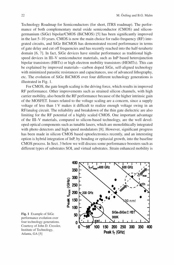
Technology Roadmap for Semiconductors (for short, ITRS roadmap). The perfor-mance of both complementary metal oxide semiconductor (CMOS) and silicon-germanium (SiGe) bipolar/CMOS (BiCMOS) [5] has been significantly improvedin the last 5–10 years. CMOS is now the main choice for radio frequency (RF) inte-grated circuits, and SiGe BiCMOS has demonstrated record performance in termsof gate delay and cut off frequencies and has recently reached into the half-terahertzdomain [6, 7]. In fact, SiGe devices have similar performance as traditional high-speed devices in III–V semiconductor materials, such as InP based heterojunctionbipolar transistors (HBTs) or high electron mobility transistors (HEMTs). This canbe explained by improved materials—carbon doped SiGe, self-aligned technologywith minimized parasitic resistances and capacitances, use of advanced lithography,etc. The evolution of SiGe BiCMOS over four different technology generations isillustrated in Fig. 1.
For CMOS, the gate length scaling is the driving force, which results in improvedRF performance. Other improvements such as strained silicon channels, with highcarrier mobility, also benefit the RF performance because of the higher intrinsic gainof the MOSFET. Issues related to the voltage scaling are a concern, since a supplyvoltage of less than 1 V makes it difficult to realize enough voltage swing in anRF/analog circuit. The reliability and breakdown of the thin gate dielectric are alsolimiting for the RF potential of a highly scaled CMOS. One important advantageof the III–V materials, compared to silicon-based technology, are the well devel-oped optical components such as tunable lasers, which are monolithically integratedwith photo detectors and high speed modulators [8]. However, significant progresshas been made in silicon CMOS based optoelectronics recently, and an interestingoption is hybrid integration of InP, by bonding or epitaxial growth, into the baselineCMOS process. In Sect. 3 below we will discuss some performance boosters such asdifferent types of substrates SOI, and virtual substrates. Strain enhanced mobility is
Fig. 1 Example of SiGeperformance evolution overfour technology generations.Courtesy of John D. Cressler,Institute of Technology,Atlanta, GA [5]
High Speed Electronics 23
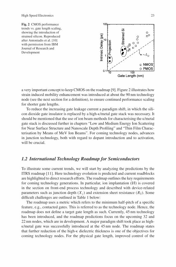
Fig. 2 CMOS performancetrends vs. gate length scaling,showing the introduction ofstrained silicon. Reproducedafter Antoniadis et al. [10]with permission from IBMJournal of Research andDevelopment
a very important concept to keep CMOS on the roadmap [9]. Figure 2 illustrates howstrain induced mobility enhancement was introduced at about the 90 nm technologynode (see the next section for a definition), to ensure continued performance scalingfor shorter gate lengths.
To reduce the increasing gate leakage current a paradigm shift, in which the sili-con dioxide gate insulator is replaced by a high-κ/metal gate stack was necessary. Itshould be mentioned that the use of ion beam methods for characterising the κ/metalgate stack is discussed further in chapters “Low and Medium Energy Ion Scatteringfor Near Surface Structure and Nanoscale Depth Profiling” and “Thin Film Charac-terisation by Means of MeV Ion Beams”. For coming technology nodes, advancesin junction technology, both with regard to dopant introduction and to activation,will be crucial.
1.2 International Technology Roadmap for Semiconductors
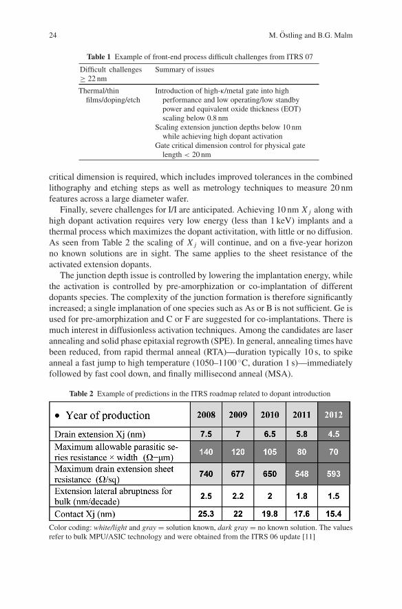
To illustrate some current trends, we will start by analyzing the predictions by theITRS roadmap [11]. Here technology evolution is predicted and current roadblocksare highlighted to direct research efforts. The roadmap outlines the key requirementsfor coming technology generations. In particular, ion implantation (I/I) is coveredin the section on front-end process technology and described with device-relatedparameters such as junction depth (X j ) and extension sheet resistance (RS). Somedifficult challenges are outlined in Table 1 below:
The roadmap uses a metric which refers to the minimum half-pitch of a specificfeature, e.g., contacted gates. This is referred to as the technology node. Hence, theroadmap does not define a target gate length as such. Currently, 45 nm technologyhas been introduced, and the roadmap predictions focus on the upcoming 32 and22 nm nodes, which are in development. A major paradigm shift took place as high-κ/metal gate was successfully introduced at the 45 nm node. The roadmap statesthat further reduction of the high-κ dielectric thickness is one of the objectives forcoming technology nodes. For the physical gate length, improved control of the
24 M. Ostling and B.G. Malm
Table 1 Example of front-end process difficult challenges from ITRS 07
Difficult challenges≥ 22 nm
Summary of issues
Thermal/thinfilms/doping/etch
Introduction of high-κ/metal gate into highperformance and low operating/low standbypower and equivalent oxide thickness (EOT)scaling below 0.8 nm
Scaling extension junction depths below 10 nmwhile achieving high dopant activation
Gate critical dimension control for physical gatelength < 20 nm
critical dimension is required, which includes improved tolerances in the combinedlithography and etching steps as well as metrology techniques to measure 20 nmfeatures across a large diameter wafer.
Finally, severe challenges for I/I are anticipated. Achieving 10 nm X j along withhigh dopant activation requires very low energy (less than 1 keV) implants and athermal process which maximizes the dopant activitation, with little or no diffusion.As seen from Table 2 the scaling of X j will continue, and on a five-year horizonno known solutions are in sight. The same applies to the sheet resistance of theactivated extension dopants.
The junction depth issue is controlled by lowering the implantation energy, whilethe activation is controlled by pre-amorphization or co-implantation of differentdopants species. The complexity of the junction formation is therefore significantlyincreased; a single implanation of one species such as As or B is not sufficient. Ge isused for pre-amorphization and C or F are suggested for co-implantations. There ismuch interest in diffusionless activation techniques. Among the candidates are laserannealing and solid phase epitaxial regrowth (SPE). In general, annealing times havebeen reduced, from rapid thermal anneal (RTA)—duration typically 10 s, to spikeanneal a fast jump to high temperature (1050–1100 ◦C, duration 1 s)—immediatelyfollowed by fast cool down, and finally millisecond anneal (MSA).
Table 2 Example of predictions in the ITRS roadmap related to dopant introduction
Color coding: white/light and gray = solution known, dark gray = no known solution. The valuesrefer to bulk MPU/ASIC technology and were obtained from the ITRS 06 update [11]
High Speed Electronics 25
2 Ion Implantation in High-Speed Device and Integrated CircuitProcess Technology
This section outlines the use of I/I in high-speed device and very large scale inte-grated (VLSI) circuit process technology with a focus on silicon CMOS devices andcircuits.
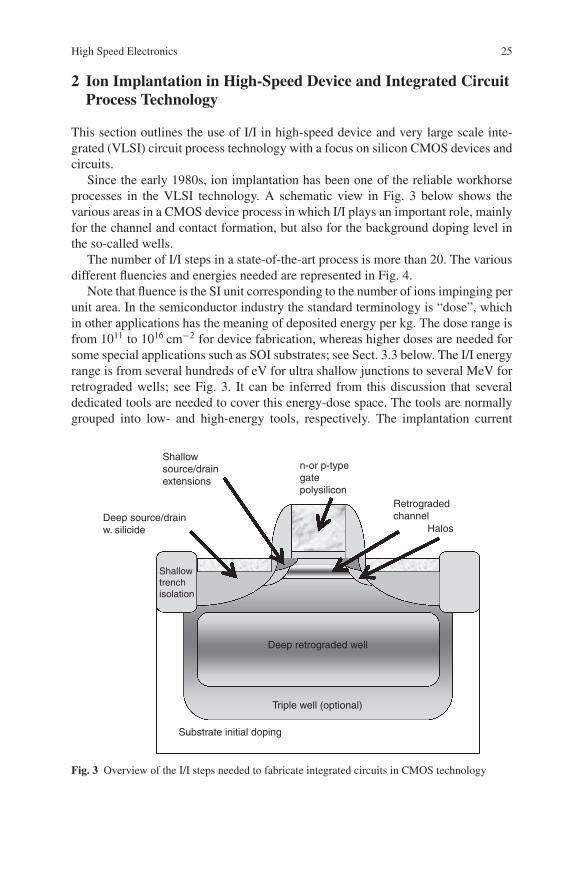
Since the early 1980s, ion implantation has been one of the reliable workhorseprocesses in the VLSI technology. A schematic view in Fig. 3 below shows thevarious areas in a CMOS device process in which I/I plays an important role, mainlyfor the channel and contact formation, but also for the background doping level inthe so-called wells.
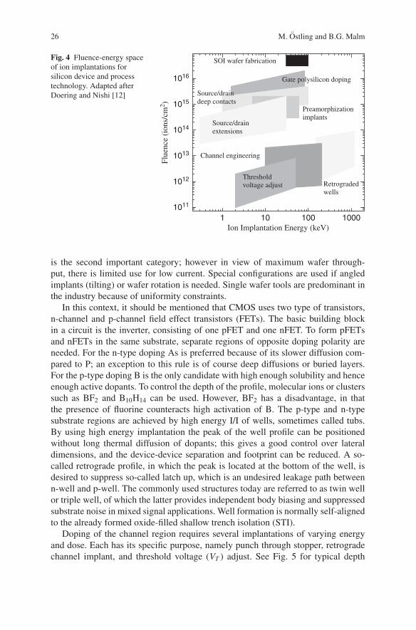
The number of I/I steps in a state-of-the-art process is more than 20. The variousdifferent fluencies and energies needed are represented in Fig. 4.
Note that fluence is the SI unit corresponding to the number of ions impinging perunit area. In the semiconductor industry the standard terminology is “dose”, whichin other applications has the meaning of deposited energy per kg. The dose range isfrom 1011 to 1016 cm−2 for device fabrication, whereas higher doses are needed forsome special applications such as SOI substrates; see Sect. 3.3 below. The I/I energyrange is from several hundreds of eV for ultra shallow junctions to several MeV forretrograded wells; see Fig. 3. It can be inferred from this discussion that severaldedicated tools are needed to cover this energy-dose space. The tools are normallygrouped into low- and high-energy tools, respectively. The implantation current
Retrogradedchannel
Shallowsource/drainextensions
Halos
Shallow trench isolation
n-or p-typegatepolysilicon
Substrate initial doping
Deep retrograded well
Triple well (optional)
Deep source/drainw. silicide
Fig. 3 Overview of the I/I steps needed to fabricate integrated circuits in CMOS technology
26 M. Ostling and B.G. Malm
Fig. 4 Fluence-energy spaceof ion implantations forsilicon device and processtechnology. Adapted afterDoering and Nishi [12]
1 10 100 10001011
1012
1013
1014
1015
1016
Preamorphizationimplants
Gate polysilicon doping
SOI wafer fabrication
Source/drain deep contacts
Thresholdvoltage adjust Retrograded
wells
Channel engineering
Source/drainextensions
Flue
nce
(ion
s/cm
2 )
Ion Implantation Energy (keV)
is the second important category; however in view of maximum wafer through-put, there is limited use for low current. Special configurations are used if angledimplants (tilting) or wafer rotation is needed. Single wafer tools are predominant inthe industry because of uniformity constraints.
In this context, it should be mentioned that CMOS uses two type of transistors,n-channel and p-channel field effect transistors (FETs). The basic building blockin a circuit is the inverter, consisting of one pFET and one nFET. To form pFETsand nFETs in the same substrate, separate regions of opposite doping polarity areneeded. For the n-type doping As is preferred because of its slower diffusion com-pared to P; an exception to this rule is of course deep diffusions or buried layers.For the p-type doping B is the only candidate with high enough solubility and henceenough active dopants. To control the depth of the profile, molecular ions or clusterssuch as BF2 and B10H14 can be used. However, BF2 has a disadvantage, in thatthe presence of fluorine counteracts high activation of B. The p-type and n-typesubstrate regions are achieved by high energy I/I of wells, sometimes called tubs.By using high energy implantation the peak of the well profile can be positionedwithout long thermal diffusion of dopants; this gives a good control over lateraldimensions, and the device-device separation and footprint can be reduced. A so-called retrograde profile, in which the peak is located at the bottom of the well, isdesired to suppress so-called latch up, which is an undesired leakage path betweenn-well and p-well. The commonly used structures today are referred to as twin wellor triple well, of which the latter provides independent body biasing and suppressedsubstrate noise in mixed signal applications. Well formation is normally self-alignedto the already formed oxide-filled shallow trench isolation (STI).
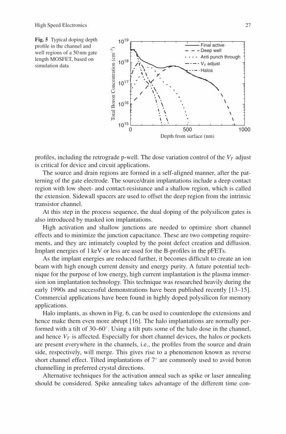
Doping of the channel region requires several implantations of varying energyand dose. Each has its specific purpose, namely punch through stopper, retrogradechannel implant, and threshold voltage (VT ) adjust. See Fig. 5 for typical depth
High Speed Electronics 27
Fig. 5 Typical doping depthprofile in the channel andwell regions of a 50 nm gatelength MOSFET, based onsimulation data
0 500 10001015
1016
1017
1018
1019
Tota
l Bor
on C
once
ntra
tion
(cm
–3)
Depth from surface (nm)
Final activeDeep wellAnti punch throughVT adjustHalos
profiles, including the retrograde p-well. The dose variation control of the VT adjustis critical for device and circuit applications.
The source and drain regions are formed in a self-aligned manner, after the pat-terning of the gate electrode. The source/drain implantations include a deep contactregion with low sheet- and contact-resistance and a shallow region, which is calledthe extension. Sidewall spacers are used to offset the deep region from the intrinsictransistor channel.
At this step in the process sequence, the dual doping of the polysilicon gates isalso introduced by masked ion implantations.
High activation and shallow junctions are needed to optimize short channeleffects and to minimize the junction capacitance. These are two competing require-ments, and they are intimately coupled by the point defect creation and diffusion.Implant energies of 1 keV or less are used for the B-profiles in the pFETs.
As the implant energies are reduced further, it becomes difficult to create an ionbeam with high enough current density and energy purity. A future potential tech-nique for the purpose of low energy, high current implantation is the plasma immer-sion ion implantation technology. This technique was researched heavily during theearly 1990s and successful demonstrations have been published recently [13–15].Commercial applications have been found in highly doped polysilicon for memoryapplications.
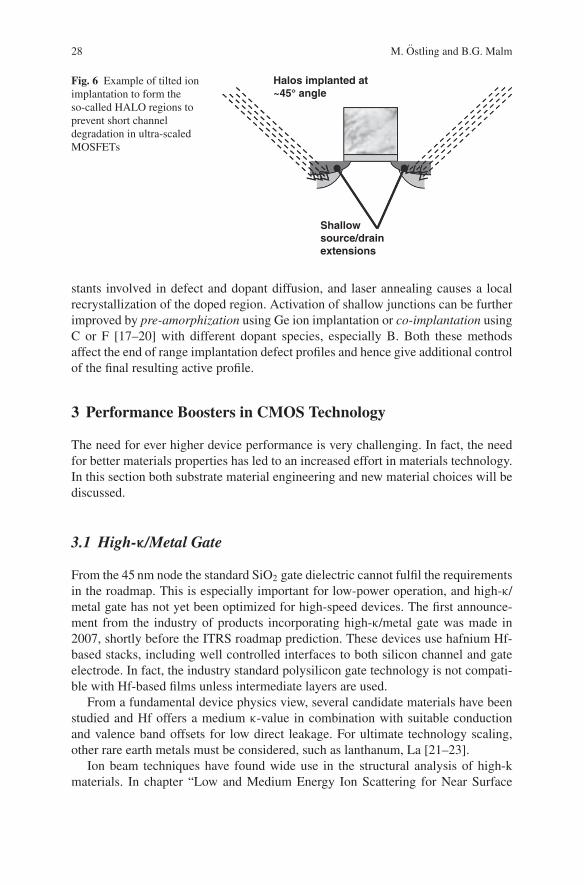
Halo implants, as shown in Fig. 6, can be used to counterdope the extensions andhence make them even more abrupt [16]. The halo implantations are normally per-formed with a tilt of 30–60◦. Using a tilt puts some of the halo dose in the channel,and hence VT is affected. Especially for short channel devices, the halos or pocketsare present everywhere in the channels, i.e., the profiles from the source and drainside, respectively, will merge. This gives rise to a phenomenon known as reverseshort channel effect. Tilted implantations of 7◦ are commonly used to avoid boronchannelling in preferred crystal directions.
Alternative techniques for the activation anneal such as spike or laser annealingshould be considered. Spike annealing takes advantage of the different time con-
28 M. Ostling and B.G. Malm
Fig. 6 Example of tilted ionimplantation to form theso-called HALO regions toprevent short channeldegradation in ultra-scaledMOSFETs
Shallowsource/drainextensions
Halos implanted at~45° angle
stants involved in defect and dopant diffusion, and laser annealing causes a localrecrystallization of the doped region. Activation of shallow junctions can be furtherimproved by pre-amorphization using Ge ion implantation or co-implantation usingC or F [17–20] with different dopant species, especially B. Both these methodsaffect the end of range implantation defect profiles and hence give additional controlof the final resulting active profile.
3 Performance Boosters in CMOS Technology
The need for ever higher device performance is very challenging. In fact, the needfor better materials properties has led to an increased effort in materials technology.In this section both substrate material engineering and new material choices will bediscussed.
3.1 High-κ/Metal Gate
From the 45 nm node the standard SiO2 gate dielectric cannot fulfil the requirementsin the roadmap. This is especially important for low-power operation, and high-κ/metal gate has not yet been optimized for high-speed devices. The first announce-ment from the industry of products incorporating high-κ/metal gate was made in2007, shortly before the ITRS roadmap prediction. These devices use hafnium Hf-based stacks, including well controlled interfaces to both silicon channel and gateelectrode. In fact, the industry standard polysilicon gate technology is not compati-ble with Hf-based films unless intermediate layers are used.
From a fundamental device physics view, several candidate materials have beenstudied and Hf offers a medium κ-value in combination with suitable conductionand valence band offsets for low direct leakage. For ultimate technology scaling,other rare earth metals must be considered, such as lanthanum, La [21–23].
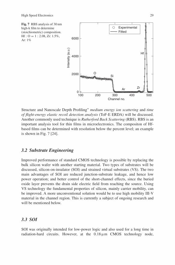
Ion beam techniques have found wide use in the structural analysis of high-kmaterials. In chapter “Low and Medium Energy Ion Scattering for Near Surface
High Speed Electronics 29
Fig. 7 RBS analysis of 30 nmhigh-k film to determine(stoichiometric) composition.Hf : O = 1 : 2.08, Zr: 1.5%,Ar: 1% 6000
4000
2000
0
Inte
nsity
(a.
u.)
500400300200100Channel no.
OSi
Zr
Hf
Ar
ExperimentalFitted
Structure and Nanoscale Depth Profiling” medium energy ion scattering and timeof flight-energy elastic recoil detection analysis (ToF-E ERDA) will be discussed.Another commonly used technique is Rutherford Back Scattering (RBS). RBS is animportant analysis tool for thin films in microelectronics. The compositon of Hf-based films can be determined with resolution below the percent level; an exampleis shown in Fig. 7 [24].
3.2 Substrate Engineering
Improved performance of standard CMOS technology is possible by replacing thebulk silicon wafer with another starting material. Two types of substrates will bediscussed, silicon-on-insulator (SOI) and strained virtual substrates (VS). The twomain advantages of SOI are reduced junction-substrate leakage, and hence lowpower operation; and better control of the short-channel effects, since the buriedoxide layer prevents the drain side electric field from reaching the source. UsingVS technology the fundamental properties of silicon, mainly carrier mobility, canbe improved. A more unconventional solution would be to use high mobility III-Vmaterial in the channel region. This is currently a subject of ongoing research andwill be mentioned below.
3.3 SOI
SOI was originally intended for low-power logic and also used for a long time inradiation-hard circuits. However, at the 0.18 μm CMOS technology node,
30 M. Ostling and B.G. Malm
SOI was introduced in microprocessors by some companies to increase theperformance/speed.
Ultrathin body SOI is one of the technologies on the roadmap beyond the current45 nm node. However, the introduction of ultrathin body SOI has been pushed backto later nodes, because of innovations in other areas.
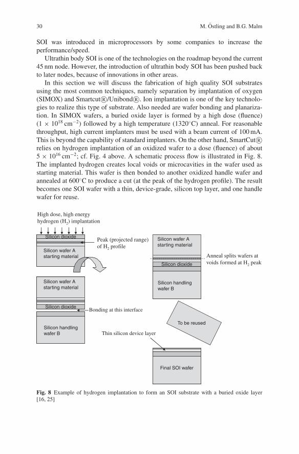
In this section we will discuss the fabrication of high quality SOI substratesusing the most common techniques, namely separation by implantation of oxygen(SIMOX) and Smartcut R©/Unibond R©. Ion implantation is one of the key technolo-gies to realize this type of substrate. Also needed are wafer bonding and planariza-tion. In SIMOX wafers, a buried oxide layer is formed by a high dose (fluence)(1 × 1018 cm−2) followed by a high temperature (1320◦C) anneal. For reasonablethroughput, high current implanters must be used with a beam current of 100 mA.This is beyond the capability of standard implanters. On the other hand, SmartCut R©relies on hydrogen implantation of an oxidized wafer to a dose (fluence) of about5 × 1016 cm−2; cf. Fig. 4 above. A schematic process flow is illustrated in Fig. 8.The implanted hydrogen creates local voids or microcavities in the wafer used asstarting material. This wafer is then bonded to another oxidized handle wafer andannealed at 600◦C to produce a cut (at the peak of the hydrogen profile). The resultbecomes one SOI wafer with a thin, device-grade, silicon top layer, and one handlewafer for reuse.
High dose, high energy hydrogen (H2) implantation
Silicon dioxide
Silicon wafer Astarting material
Peak (projected range) of H2 profile
Silicon wafer A
starting material
Silicon dioxide
Silicon wafer Astarting material
Silicon dioxide
Silicon handling
wafer B
Silicon handlingwafer B
Bonding at this interface
Silicon wafer Astarting material
Silicon dioxide
Silicon handling
wafer B
Silicon handlingwafer B
Anneal splits wafers at voids formed at H2 peak
To be reused
Final SOI waferFinal SOI wafer
Thin silicon device layer
Fig. 8 Example of hydrogen implantation to form an SOI substrate with a buried oxide layer[16, 25]
High Speed Electronics 31
3.4 Virtual Substrates
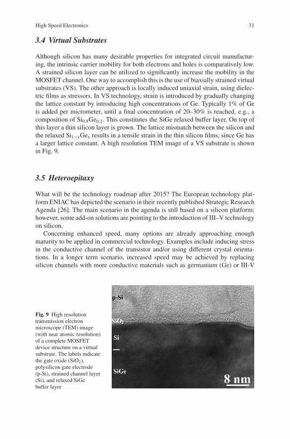
Although silicon has many desirable properties for integrated circuit manufactur-ing, the intrinsic carrier mobility for both electrons and holes is comparatively low.A strained silicon layer can be utilized to significantly increase the mobility in theMOSFET channel. One way to accomplish this is the use of biaxially strained virtualsubstrates (VS). The other approach is locally induced uniaxial strain, using dielec-tric films as stressors. In VS technology, strain is introduced by gradually changingthe lattice constant by introducing high concentrations of Ge. Typically 1% of Geis added per micrometer, until a final concentration of 20–30% is reached, e.g., acomposition of Si0.8Ge0.2. This constitutes the SiGe relaxed buffer layer. On top ofthis layer a thin silicon layer is grown. The lattice mismatch between the silicon andthe relaxed Si1−xGex results in a tensile strain in the thin silicon films, since Ge hasa larger lattice constant. A high resolution TEM image of a VS substrate is shownin Fig. 9.
3.5 Heteroepitaxy
What will be the technology roadmap after 2015? The European technology plat-form ENIAC has depicted the scenario in their recently published Strategic ResearchAgenda [26]. The main scenario in the agenda is still based on a silicon platform;however, some add-on solutions are pointing to the introduction of III–V technologyon silicon.
Concerning enhanced speed, many options are already approaching enoughmaturity to be applied in commercial technology. Examples include inducing stressin the conductive channel of the transistor and/or using different crystal orienta-tions. In a longer term scenario, increased speed may be achieved by replacingsilicon channels with more conductive materials such as germanium (Ge) or III-V
Fig. 9 High resolutiontransmission electronmicroscope (TEM) image(with near atomic resolution)of a complete MOSFETdevice structure on a virtualsubstrate. The labels indicatethe gate oxide (SiO2),polysilicon gate electrode(p-Si), strained channel layer(Si), and relaxed SiGebuffer layer
32 M. Ostling and B.G. Malm
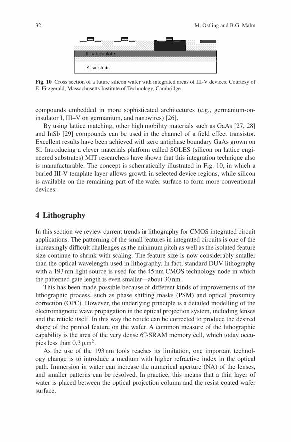
Fig. 10 Cross section of a future silicon wafer with integrated areas of III-V devices. Courtesy ofE. Fitzgerald, Massachusetts Institute of Technology, Cambridge
compounds embedded in more sophisticated architectures (e.g., germanium-on-insulator I, III–V on germanium, and nanowires) [26].
By using lattice matching, other high mobility materials such as GaAs [27, 28]and InSb [29] compounds can be used in the channel of a field effect transistor.Excellent results have been achieved with zero antiphase boundary GaAs grown onSi. Introducing a clever materials platform called SOLES (silicon on lattice engi-neered substrates) MIT researchers have shown that this integration technique alsois manufacturable. The concept is schematically illustrated in Fig. 10, in which aburied III-V template layer allows growth in selected device regions, while siliconis available on the remaining part of the wafer surface to form more conventionaldevices.
4 Lithography
In this section we review current trends in lithography for CMOS integrated circuitapplications. The patterning of the small features in integrated circuits is one of theincreasingly difficult challenges as the minimum pitch as well as the isolated featuresize continue to shrink with scaling. The feature size is now considerably smallerthan the optical wavelength used in lithography. In fact, standard DUV lithographywith a 193 nm light source is used for the 45 nm CMOS technology node in whichthe patterned gate length is even smaller—about 30 nm.
This has been made possible because of different kinds of improvements of thelithographic process, such as phase shifting masks (PSM) and optical proximitycorrection (OPC). However, the underlying principle is a detailed modelling of theelectromagnetic wave propagation in the optical projection system, including lensesand the reticle itself. In this way the reticle can be corrected to produce the desiredshape of the printed feature on the wafer. A common measure of the lithographiccapability is the area of the very dense 6T-SRAM memory cell, which today occu-pies less than 0.3 μm2.
As the use of the 193 nm tools reaches its limitation, one important technol-ogy change is to introduce a medium with higher refractive index in the opticalpath. Immersion in water can increase the numerical aperture (NA) of the lenses,and smaller patterns can be resolved. In practice, this means that a thin layer ofwater is placed between the optical projection column and the resist coated wafersurface.
High Speed Electronics 33
Much effort is also placed on light sources with shorter wavelength, so-calledextreme ultraviolet (EUV). This will be accompanied by a change in the opticswhich will be reflective (using mirrors) instead of refractive (lenses). Masks whichare transparent to these wavelengths are also needed.
The alternatives to optical lithography using reticles are based on direct-writingtechniques, in which an electron beam is widely used for nanostructures and forspecial applications, such as dense optical gratings. Focused ion beam (FIB) sys-tems have also been proposed. For an extensive treatment of FIB, refer to chap-ter “Focused Ion Beam Machining and Deposition”. Typically, ions such as Ga+
(atomic mass 31) are used. For FIB lithography, lighter ions such as protons(H+) may be used; for more details see chapter “Proton Beam Writing: A New3D Nano Lithographic Technique”. Some of the issues here are wafer throughputand line edge roughness due to electron/ion scattering. Electron beam systems arewidely used for lithographic reticle (mask) manufacturing. FIB is used for maskrepair and also for postprocessing analysis and correction of failures in integratedcircuits.
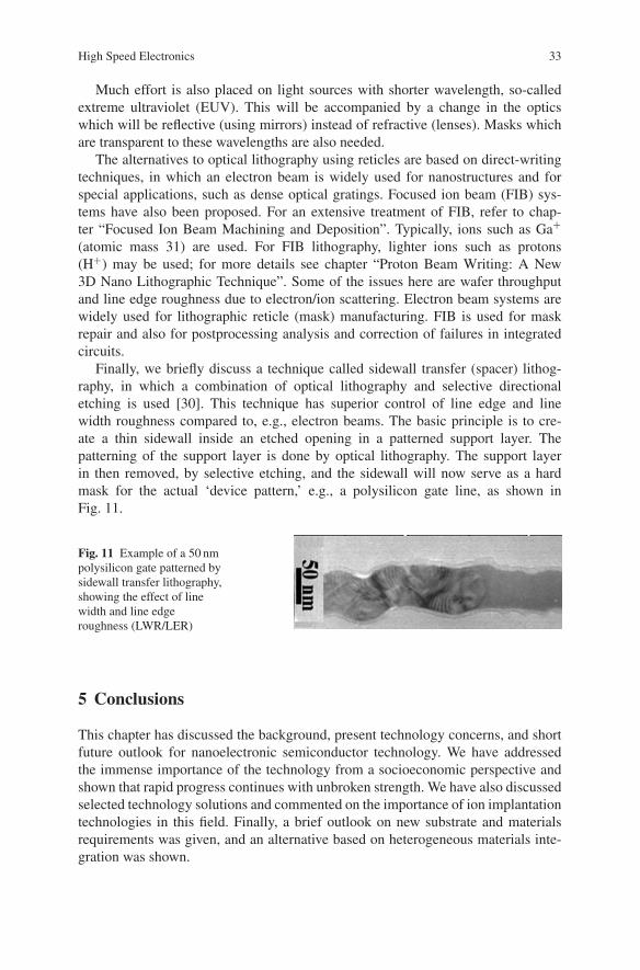
Finally, we briefly discuss a technique called sidewall transfer (spacer) lithog-raphy, in which a combination of optical lithography and selective directionaletching is used [30]. This technique has superior control of line edge and linewidth roughness compared to, e.g., electron beams. The basic principle is to cre-ate a thin sidewall inside an etched opening in a patterned support layer. Thepatterning of the support layer is done by optical lithography. The support layerin then removed, by selective etching, and the sidewall will now serve as a hardmask for the actual ‘device pattern,’ e.g., a polysilicon gate line, as shown inFig. 11.
Fig. 11 Example of a 50 nmpolysilicon gate patterned bysidewall transfer lithography,showing the effect of linewidth and line edgeroughness (LWR/LER)
5 Conclusions
This chapter has discussed the background, present technology concerns, and shortfuture outlook for nanoelectronic semiconductor technology. We have addressedthe immense importance of the technology from a socioeconomic perspective andshown that rapid progress continues with unbroken strength. We have also discussedselected technology solutions and commented on the importance of ion implantationtechnologies in this field. Finally, a brief outlook on new substrate and materialsrequirements was given, and an alternative based on heterogeneous materials inte-gration was shown.
34 M. Ostling and B.G. Malm
References
1. Moore GE, Cramming more components onto integrated circuits, Electronics, 38,114–117, (1965).
2. Takeuchi K, Tatsumi T, and Furukawa A, Channel engineering for the reduction of random-dopant-placement-induced threshold voltage fluctuation, Technical Digest of the InternationalElectron Device Meeting, 841–844, (1997).
3. Wettstein A, Penzin O, Lyumkis E, et al., Random dopant fluctuation modelling with theimpedance field method, Proceedings of International Conference on Simulation of Semicon-ductor Devices and Processes, 91–94, (2003).
4. Ohtou T, Sugii N, and Hiramoto T, Impact of parameter variations and random dopant fluctua-tions on short-channel fully depleted SOI MOSFETS with extremely thin box, IEEE ElectronDevice Letters, 28, 740–742, (2007).
5. Cressler JD and Niu G, Silicon-Germanium Heterojunction Bipolar Transistors. Norwood,MA: Artech House, 2003.
6. Chevalier P, Zerounian N, Barbalat B, et al., On the use of cryogenic measurements toinvestigate the potential of Si/SiGe:C HBTs for terahertz operation, Proceedings of Bipo-lar/BiCMOS Circuits and Technology Meeting, 26–29, (2007).
7. Krithivasan R, Yuan L, Cressler JD, et al., Half-terahertz operation of SiGe HBTs, IEEEElectron Device Letters, 27, 567–569, (2006).
8. Westergren U, Yu Y, and Thylen L, High-speed travelling-wave electro-absorption mod-ulators, Proceedings of SPIE – The International Society for Optical Engineering, 6350,635004, (2006).
9. Thompson SE, Armstrong M, Auth C, et al., A logic nanotechnology featuring strained-silicon, IEEE Electron Device Letters, 25, 191–193, (2004).
10. Antoniadis DA, Aberg I, NıChleirigh C, et al., Continuous MOSFET performance increasewith device scaling: The role of strain and channel material innovations, IBM Journal ofResearch and Development, 50, 363–376A, (2006).
11. International Technology Roadmap for Semiconductors (ITRS) 2006 update, 2006.12. Doering R and Nishi Y, Handbook of Semiconductor Manufacturing Technology, 2nd ed.
Boca Raton, FL: CRC Press, Taylor & Francis Group, 2008.13. Kilho L, Plasma immersion ion implantation as an alternative doping technology for
ULSI, Extended Abstracts of the Second International Workshop on Junction Technology,21–27, (2001).
14. Agarwal A and Kushner MJ, Characteristics of pulsed plasma doping (P2LAD) sources forultra-shallow junction formation, Proceedings of IEEE International Conference on PlasmaScience, 14, (2005).
15. Current MI, Plasma immersion implantation for modification and doping of semiconductormaterials: A historical perspective: 1886 to 2000, Extended Abstracts of the First Interna-tional Workshop on Junction Technology, 13–17, (2000).
16. Chen W-K, The VLSI Handbook, 2nd ed. Boca Raton, FL: CRC Press, Taylor & FrancisGroup, 2006.
17. Augendre E, Pawlak BJ, Kubicek S, et al., Superior N- and PMOSFET scalability using car-bon co-implantation and spike annealing, Proceedings of 36th European Solid-State DeviceResearch Conference, 355–358, (2006).
18. Yamamoto T, Kubo T, Sukegawa T, et al., Advanced junction profile engineering featuringlaser spike annealing and co-implantation for sub-30-nm strained CMOS devices, TechnicalDigest of Symposium on VLSI Technology 2, (2006).
19. Kubicek S, Hoffmann T, Augendre E, et al., Superior nMOSFET scalability using Fluorineineco-implantation and spike annealing, Proceedings of International Conference on AdvancedSemiconductor Devices and Microsystems, 101–104, (2006).
High Speed Electronics 35
20. Pawlak B, Lindsay R, Surdeanu R, et al., Optimizing p-type ultra-shallow junctions for the65 nm CMOS technology node, 14th International Conference on Ion Implantation Technol-ogy Proceedings, 21–24, (2003).
21. Robertson J, Band structures and band offsets of high K dielectrics on Si, Applied SurfaceScience, 190, 2–10, (2002).
22. Iwai H, Ohmi S, Akama S, et al., Advanced gate dielectric materials for sub-100 nm CMOS,Technical Digest of International Electron Device Meeting, 625–628, (2002).
23. Engstrom O, Raeissi B, Hall S, et al., Navigation aids in the search for future high-kdielectrics: Physical and electrical trends, Solid-State Electronics, 51, 622–626, (2007).
24. Malm BG, Sjoblom G, Martin D, et al., Unpublished Results, (2007).25. Wolf S and Tauber RN, Silicon Processing for the VLSI era Volume 1 – Process Technology,
2nd ed. Sunset Beach, CA: Lattice Press, 2000.26. Eniac strategic research agenda, http://www.eniac.eu/web/downloads/SRA2007.pdf, 2007.27. Fitzgerald EA, Dohrman CL, Chilukuri K, et al., Epitaxial growth of heterovalent GaAs/Ge
and applications in III–V monolithic integration on Si substrates, ECS Transactions, SiGe andGe: Materials, Processing, and Devices, 3, 561–568, (2006).
28. Carlin JA, Andre CL, Kwon O, et al., III–V device integration on silicon via metamorphicSiGe substrates, ECS Transactions, SiGe and Ge: Materials, Processing, and Devices, 3,729–743, (2006).
29. Datta S, Ashley T, Brask J, et al., 85 nm gate length enhancement and depletion mode InSbquantum well transistors for ultra high speed and very low power digital logic applications,Technical Digest of International Electron Devices Meeting, 763–766, (2005).
30. Hallstedt J, Hellstrom P-E, Zhang Z, et al., A robust spacer gate process for deca-nanometerhigh-frequency MOSFETs, Microelectronic Engineering, 83, 434–439, (2006).