Embed Size (px)
Citation preview
IPC-A-610DCTelecom Addendum
August 2009
A standard developed by IPC
®
Association Connecting Electronics Industries
The Principles ofStandardization
In May 1995 the IPC’s Technical Activities Executive Committee (TAEC) adopted Principles ofStandardization as a guiding principle of IPC’s standardization efforts.
Standards Should:• Show relationship to Design for Manufacturability
(DFM) and Design for the Environment (DFE)• Minimize time to market• Contain simple (simplified) language• Just include spec information• Focus on end product performance• Include a feedback system on use and
problems for future improvement
Standards Should Not:• Inhibit innovation• Increase time-to-market• Keep people out• Increase cycle time• Tell you how to make something• Contain anything that cannot
be defended with data
Notice IPC Standards and Publications are designed to serve the public interest through eliminating mis-understandings between manufacturers and purchasers, facilitating interchangeability and improve-ment of products, and assisting the purchaser in selecting and obtaining with minimum delay theproper product for his particular need. Existence of such Standards and Publications shall not inany respect preclude any member or nonmember of IPC from manufacturing or selling productsnot conforming to such Standards and Publication, nor shall the existence of such Standards andPublications preclude their voluntary use by those other than IPC members, whether the standardis to be used either domestically or internationally.
Recommended Standards and Publications are adopted by IPC without regard to whether their adop-tion may involve patents on articles, materials, or processes. By such action, IPC does not assumeany liability to any patent owner, nor do they assume any obligation whatever to parties adoptingthe Recommended Standard or Publication. Users are also wholly responsible for protecting them-selves against all claims of liabilities for patent infringement.
IPC PositionStatement onSpecificationRevision Change
It is the position of IPC’s Technical Activities Executive Committee that the use and implementationof IPC publications is voluntary and is part of a relationship entered into by customer and supplier.When an IPC publication is updated and a new revision is published, it is the opinion of the TAECthat the use of the new revision as part of an existing relationship is not automatic unless requiredby the contract. The TAEC recommends the use of the latest revision. Adopted October 6, 1998
Why is therea charge forthis document?
Your purchase of this document contributes to the ongoing development of new and updated industrystandards and publications. Standards allow manufacturers, customers, and suppliers to understandone another better. Standards allow manufacturers greater efficiencies when they can set up theirprocesses to meet industry standards, allowing them to offer their customers lower costs.
IPC spends hundreds of thousands of dollars annually to support IPC’s volunteers in the standardsand publications development process. There are many rounds of drafts sent out for review andthe committees spend hundreds of hours in review and development. IPC’s staff attends and par-ticipates in committee activities, typesets and circulates document drafts, and follows all necessaryprocedures to qualify for ANSI approval.
IPC’s membership dues have been kept low to allow as many companies as possible to participate.Therefore, the standards and publications revenue is necessary to complement dues revenue. Theprice schedule offers a 50% discount to IPC members. If your company buys IPC standards andpublications, why not take advantage of this and the many other benefits of IPC membership aswell? For more information on membership in IPC, please visit www.ipc.org or call 847/597-2872.
Thank you for your continued support.
©Copyright 2009. IPC, Bannockburn, Illinois, USA. All rights reserved under both international and Pan-American copyright conventions. Anycopying, scanning or other reproduction of these materials without the prior written consent of the copyright holder is strictly prohibited andconstitutes infringement under the Copyright Law of the United States.
IPC-A-610DC
Telecom Addendum
Developed by the Telecom IPC-A-610 Addendum Task Group (7-31bc) ofthe Product Assurance Committee (7-30) of IPC
Users of this standard are encouraged to participate in thedevelopment of future revisions.
Contact:
IPC3000 Lakeside Drive, Suite 309SBannockburn, Illinois60015-1249Tel 847 615.7100Fax 847 615.7105
®
AcknowledgmentMembers of the Telecom IPC-A-610 Addendum Task Group have worked together to develop this document. We would liketo thank them for their dedication to this effort. Any document involving a complex technology draws material from a vastnumber of sources. While the principal members of the Telecom IPC-A-610 Addendum Task Group (7-31bc) of the Prod-uct Assurance Committee (7-30) are shown below, it is not possible to include all of those who assisted in the evolution ofthis standard. To each of them, the members of the IPC extend their gratitude.
Product AssuranceCommittee
IPC-A-610 TelecomAddendum Task Group
Technical Liaisons of theIPC Board of Directors
ChairMel ParrishSTI Electronics
ChairDarrin DodsonAlcetel-Lucent
Peter BigelowIMI Inc.
Sammy YiAptina Imaging Corporation
Members of the IPC-A-610 Telecom Addendum Task Group
Tom Bennett, Adtran Inc.Trevor Bowers, Adtran Inc.Darrin Dodson, Alcatel-LucentChristopher Sattler, AQS - All
Quality & Services, Inc.Joe Bartnicki, Fujitsu Network
CommunicationsSteven Smith, Fujitsu Network
Communications
Michael Nadreau, HenkelCorporation
Bai Chun Xiang, HuaweiTechnologies Co., Ltd.
Stephen Tisdale, Intel CorporationVasu Vasudevan, Intel CorporationGirish Wable, Jabil Circuit, Inc. (HQ)Beverley Christian, Research In
Motion Limited
Jennifer Day, Sanmina-SCIOfer Cohen, Seabridge Ltd., A
Siemens CompanyMel Parrish, STI ElectronicsTodd Herman, TellabsBob Willis, The SMART Group
SPECIAL ACKNOWLEDGMENT
We would like to provide special acknowledgment to the following member for providing pictures and illustrations thatare used in this revision.
Darrin Dodson, Alcatel-Lucent
August 2009 IPC-A-610DC
ii
0.1 Scope This addendum provides requirements to be used in addition to, and in some cases, in place of, those published inIPC-A-610D to ensure that electrical and electronic assemblies meet requirements for customers requiring Telecordia GR-78-CORE compliance.
Where content criteria are not supplemented, the Class 2 requirements of IPC-A-610D apply.
0.1.1 Purpose When required by procurement documentation/drawings, this Addendum supplements or replaces specificallyidentified requirements of IPC-A-610D.
0.1.2 Precedence Customer contractual requirements take precedence over this Addendum, referenced standards and user-approved drawings. In the event of a conflict between this Addendum and the applicable documents cited herein, this Addendumtakes precedence. Where referenced criteria of this addendum differ from the published IPC-A-610D, this addendum takes pre-cedence.
0.1.3 Existing or Previously Approved Designs This Addendum shall not constitute the sole cause for the redesign of pre-viously approved designs. When drawings for existing or previously approved designs undergo revision they should be reviewedand changes made that allow for compliance with the requirements of this Addendum.
0.1.4 Use This Addendum is applicable for rigid single sided, double sided, and multilayer boards.
This Addendum shall not to be used as a standalone document.
Where criteria are not supplemented, the Class 2 requirements of IPC-A-610D apply. Criteria defined in IPC-A-601D as ‘‘processdefects’’ for class 2 shall be treated as defective, unless otherwise stated in this Addendum.
If an IPC-A-610D requirement is changed or added by this Addendum, the clause is identified and that entire IPC-A-610D clauseor subordinate clause is replaced by the criteria in this Addendum.
The clauses modified by this Addendum do not include subordinate clauses unless specifically stated (e.g., 1.4 does not include1.4.1). Clauses, Tables, Figures, etc., in IPC-A-610D that are not listed in this Addendum are to be used as-published.
In this addendum, as in the published IPC-A-610D, in case of conflict or discrepancy, the description or written crite-ria always take precedence over the illustrations.
The surface insulation resistance and the electromigration resistance of the finished PBA shall be in accordance with GR-78-CORE. This is relevant for no-clean assembly processes, which should be used preferably, as well as for fluxes which are intendedto be cleaned, and for SMC adhesives.
Solder alloy shall comply with J-STD-006 or equivalent.
0.1.5 Additional Referenced Standards Telcordia GR-78-CORE Generic Requirements for the Physical Design and Manufac-ture of Telecommunications Products and Equipment (http://telecom-info.telcordia.com).
Telecom Addendum
1A-610DC August 2009
These criteria replace all of 1.4.5 in published IPC-A-610D.
Minimum electrical clearance for products built to this document is specified as 0.13 mm [.005 in].
These criteria replace all of 4.1.3 in published IPC-A-610D.
Defect
• Less than one and one-half thread extends beyond thethreaded hardware, (e.g., nut) unless thread extensionwould interfere with other component.
• Thread extension more than 3 mm [0.12 in] plus one andone-half threads for bolts or screws up to 25 mm [0.984 in].
• Thread extension more than 6.3 mm [0.248 in] plus one andone-half threads for bolts or screws over 25 mm [0.984 in].
• Bolts or screws without locking mechanisms.
These criteria replace all of 4.1.3.1 in published IPC-A-610D.
When connections are made using threaded fasteners they must be tight to ensure the reliability of the connection. When split-ring type lock washers are used, the threaded fastener must be tight enough to compress the lock washer. Fastener torque value,if not specified, shall be specified by engineering documentation.
Acceptable
• Fasteners are tight and split-ring lock washers, when used,are fully compressed.
• Fasteners torque values are within the limits as specified bydrawing, or as specified by engineering documentation.
Defect
• Split-ring lock washer not compressed.
• Fasteners are not properly torqued within the limits specifiedby drawing, or as specified by engineering documentation.
Criteria in published IPC-A-610D 4.1.3.2 are not applicable to users of this addendum.
Telecom Addendum
1.4.5 Electrical Clearance
2 A-610DCAugust 2009
4.1.3 Hardware Installation – Threaded Fasteners
4.1.3.2 Hardware Installation – Threaded Fasteners – Wires
4.1.3.1 Hardware Installation – Threaded Fasteners – Torque

These criteria replace all of 4.3.2 in published IPC-A-610D.
Acceptable
• Damaged nonfunctional lands for single and double-sidedboards are acceptable if firmly attached to board in unliftedareas.
Defect
• Any functional annular ring which is lifted.
These criteria replace all of 4.4.1 in published IPC-A-610D.
Metal cable clamps shall not be used unless they are insulated.
Acceptable
• The wires are secured in the wire bundle.
• Cable ties are cut flush with the locking head.
Defect
• Spot tie wrap or knot is loose.
• Wire bundle is loose.
• Cable tied with an improper knot. This tie may eventuallyloosen.
• Restraining devices, clamps, plastic ties, lacing cord, etc.damages the wiring insulation or cable by compression.
• End of cut tie wrap protrudes past the face of the lockinghead.
This replaces Table 4-1 in 4.5.2 of published IPC-A-610D. All of the rest of 4.5.2 in published IPC-A-610D is applicable.
IPC-A-610DC Table 4-1 Minimum Bend Radius Requirements
Cable Type IPC-A-610DC
Bare bus or enamel insulated wire 2X
Insulated wire and flat ribbon cable 2X
Cable bundles with no coax cables 2X
Cable bundles with coax cables 5X
Coaxial cables 5X
CAT5 Ethernet cable 4X
Fiber Optic Cable - Buffered and Jacketed Single Fiber 1 inch or as specified by the manufacturer
Larger jacketed fibers 15X cable diameter or as specified by the manufacturer
Telecom Addendum
4.3.2 Connector Pins – Press Fit Pins
3A-610DC August 2009
4.4.1 Wire Bundle Securing – General
4.5.2 Routing – Bend Radius
These criteria replace all of 4.5.3 in published IPC-A-610D.
Defect
• Inside bend radii does not meet the criteria of Table 4-1.
Defect
• Spot ties or tie wraps that cause any deformation of coaxialcables.
These criteria replace all of 5.2.1 in published IPC-A-610D.
Process Indicator
• Exposed basis metal on component leads, conductors orland surfaces from nicks or scratches provided conditionsdo not exceed the requirements of 7.1.2.3 for leads and10.2.9.1 for conductors and lands.
These criteria replace all of 5.2.2 in published IPC-A-610D.
Process Indicator
• Blowholes, pinholes, voids, etc., providing the solder con-nection meets all other requirements.
Use 7.1 published criteria in IPC-A-610D with this added statement:
The presence of engineering approved spacers or insulators, used to improve manufacturability, shall not be cause for rejection.
Telecom Addendum
4.5.3 Routing – Coaxial Cable
4 A-610DCAugust 2009
5.2.1 Soldering Anomalies – Exposed Basis Metal
7.1 Component Mounting
5.2.2 Soldering Anomalies – Pin Holes/Blow Holes
These criteria replace all of 7.1.7 in published IPC-A-610D.
Target
• The component body is in flat contact with the board’s sur-face.
Acceptable
• Component in contact with board on at least one sideand/or surface.
Note: When documented on an approved assembly drawing,a component may be either side mounted or end mounted.The side or surface of the body, or at least one point of anyirregularly configured component (such as certain pocketbookcapacitors), needs to be in full contact with the printed board.
The body shall be bonded or otherwise secured to the boardto prevent damage when vibration and shock forces areapplied.
Defect
• Component not secured.
These criteria replace all of 7.1.8 in published IPC-A-610D.
These criteria apply to soldered connectors and unsoldered press fit connectors. For connector pin criteria see 4.3. For connec-tor damage criteria see 9.5.
Connector module/pin misalignment, defined in this section, is to be measured at the connector lead-in area/hole (for receptacles)or at the pin tip (for pin headers).
In cases where an assembly connector is composed of two or more identical connector modules, it shall not be permissible tomix modules manufactured by different suppliers.
Telecom Addendum
7.1.7 Component Mounting – Radial Leads – Horizontal
5A-610DC August 2009
7.1.8 Component Mounting – Connectors
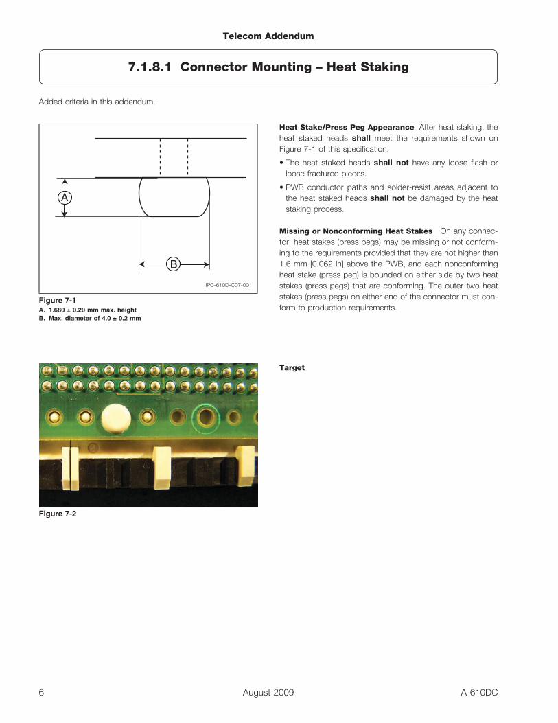
Added criteria in this addendum.
Heat Stake/Press Peg Appearance After heat staking, theheat staked heads shall meet the requirements shown onFigure 7-1 of this specification.
• The heat staked heads shall not have any loose flash orloose fractured pieces.
• PWB conductor paths and solder-resist areas adjacent tothe heat staked heads shall not be damaged by the heatstaking process.
Missing or Nonconforming Heat Stakes On any connec-tor, heat stakes (press pegs) may be missing or not conform-ing to the requirements provided that they are not higher than1.6 mm [0.062 in] above the PWB, and each nonconformingheat stake (press peg) is bounded on either side by two heatstakes (press pegs) that are conforming. The outer two heatstakes (press pegs) on either end of the connector must con-form to production requirements.
Target
IPC-610D-C07-001
Figure 7-1A. 1.680 ± 0.20 mm max. heightB. Max. diameter of 4.0 ± 0.2 mm
B
A
Figure 7-2
Telecom Addendum
7.1.8.1 Connector Mounting – Heat Staking
6 A-610DCAugust 2009
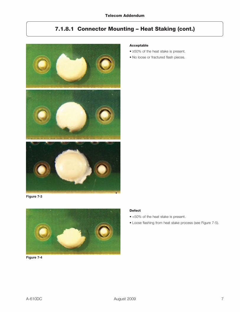
Acceptable
• ≥50% of the heat stake is present.
• No loose or fractured flash pieces.
Defect
• <50% of the heat stake is present.
• Loose flashing from heat stake process (see Figure 7-5).
Figure 7-3
Figure 7-4
Telecom Addendum
7.1.8.1 Connector Mounting – Heat Staking (cont.)
7A-610DC August 2009

Added criteria in this addendum.
Target
• Connector is mounted flush with the surface of the board.
Acceptable
• Connector-to-board spacing is equal to or less than 0.25mm [0.010 in] (not shown).
Defect
• Connector to board spacing is greater than 0.25 mm [0.010in] (not shown).
Figure 7-5
Figure 7-6
Telecom Addendum
7.1.8.1 Connector Mounting – Heat Staking (cont.)
8 A-610DCAugust 2009
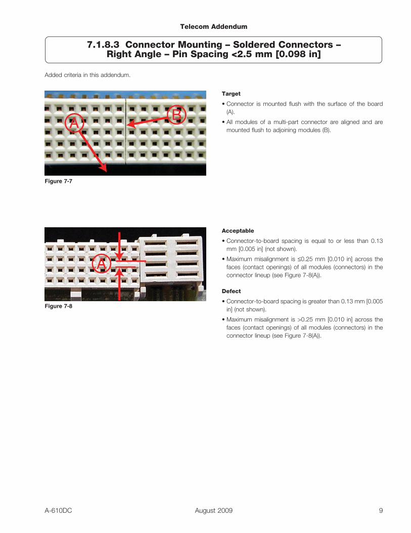
7.1.8.2 Connector Mounting – Soldered Connectors –Right Angle – Pin Spacing ≥2.5 mm [0.098 in]
Added criteria in this addendum.
Target
• Connector is mounted flush with the surface of the board(A).
• All modules of a multi-part connector are aligned and aremounted flush to adjoining modules (B).
Acceptable
• Connector-to-board spacing is equal to or less than 0.13mm [0.005 in] (not shown).
• Maximum misalignment is ≤0.25 mm [0.010 in] across thefaces (contact openings) of all modules (connectors) in theconnector lineup (see Figure 7-8(A)).
Defect
• Connector-to-board spacing is greater than 0.13 mm [0.005in] (not shown).
• Maximum misalignment is >0.25 mm [0.010 in] across thefaces (contact openings) of all modules (connectors) in theconnector lineup (see Figure 7-8(A)).
Figure 7-7
Figure 7-8
Telecom Addendum
7.1.8.3 Connector Mounting – Soldered Connectors –Right Angle – Pin Spacing <2.5 mm [0.098 in]
9A-610DC August 2009
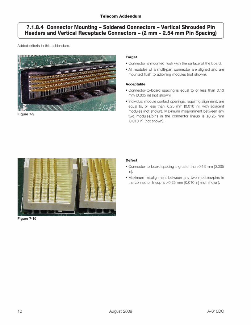
Added criteria in this addendum.
Target
• Connector is mounted flush with the surface of the board.
• All modules of a multi-part connector are aligned and aremounted flush to adjoining modules (not shown).
Acceptable
• Connector-to-board spacing is equal to or less than 0.13mm [0.005 in] (not shown).
• Individual module contact openings, requiring alignment, areequal to, or less than, 0.25 mm [0.010 in], with adjacentmodules (not shown). Maximum misalignment between anytwo modules/pins in the connector lineup is ≤0.25 mm[0.010 in] (not shown).
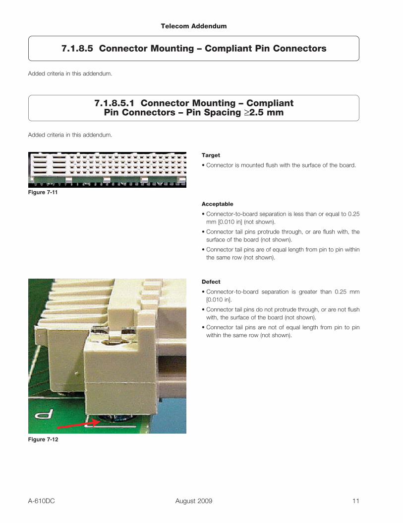
Defect
• Connector-to-board spacing is greater than 0.13 mm [0.005in].
• Maximum misalignment between any two modules/pins inthe connector lineup is >0.25 mm [0.010 in] (not shown).
Figure 7-9
Figure 7-10
Telecom Addendum
7.1.8.4 Connector Mounting – Soldered Connectors – Vertical Shrouded PinHeaders and Vertical Receptacle Connectors – (2 mm - 2.54 mm Pin Spacing)
10 A-610DCAugust 2009
Added criteria in this addendum.
Added criteria in this addendum.
Target
• Connector is mounted flush with the surface of the board.
Acceptable
• Connector-to-board separation is less than or equal to 0.25mm [0.010 in] (not shown).
• Connector tail pins protrude through, or are flush with, thesurface of the board (not shown).
• Connector tail pins are of equal length from pin to pin withinthe same row (not shown).
Defect
• Connector-to-board separation is greater than 0.25 mm[0.010 in].
• Connector tail pins do not protrude through, or are not flushwith, the surface of the board (not shown).
• Connector tail pins are not of equal length from pin to pinwithin the same row (not shown).
Figure 7-11
Figure 7-12
Telecom Addendum
7.1.8.5 Connector Mounting – Compliant Pin Connectors
11A-610DC August 2009
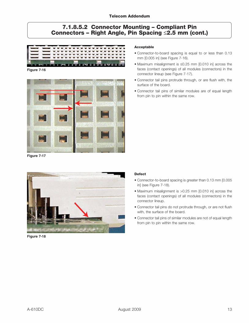
7.1.8.5.1 Connector Mounting – CompliantPin Connectors – Pin Spacing ≥2.5 mm
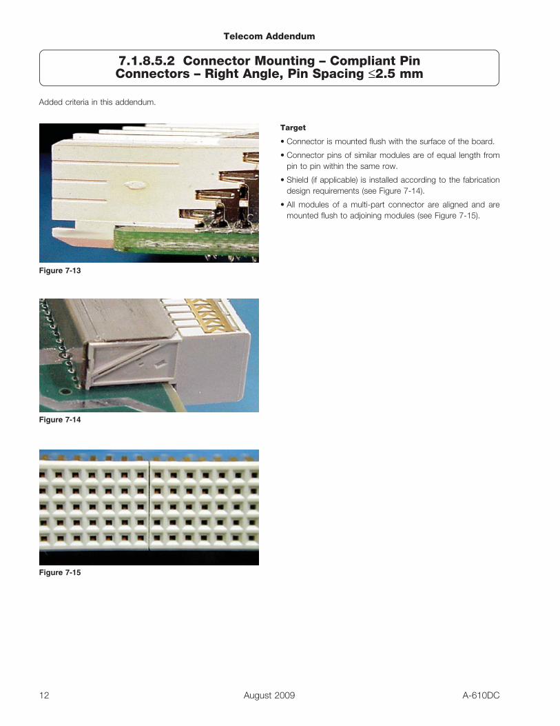
Added criteria in this addendum.
Target
• Connector is mounted flush with the surface of the board.
• Connector pins of similar modules are of equal length frompin to pin within the same row.
• Shield (if applicable) is installed according to the fabricationdesign requirements (see Figure 7-14).
• All modules of a multi-part connector are aligned and aremounted flush to adjoining modules (see Figure 7-15).
Figure 7-13
Figure 7-14
Figure 7-15
Telecom Addendum
7.1.8.5.2 Connector Mounting – Compliant PinConnectors – Right Angle, Pin Spacing ≤2.5 mm
12 A-610DCAugust 2009
Acceptable
• Connector-to-board spacing is equal to or less than 0.13mm [0.005 in] (see Figure 7-16).
• Maximum misalignment is ≤0.25 mm [0.010 in] across thefaces (contact openings) of all modules (connectors) in theconnector lineup (see Figure 7-17).
• Connector tail pins protrude through, or are flush with, thesurface of the board.
• Connector tail pins of similar modules are of equal lengthfrom pin to pin within the same row.
Defect
• Connector-to-board spacing is greater than 0.13 mm [0.005in] (see Figure 7-18).
• Maximum misalignment is >0.25 mm [0.010 in] across thefaces (contact openings) of all modules (connectors) in theconnector lineup.
• Connector tail pins do not protrude through, or are not flushwith, the surface of the board.
• Connector tail pins of similar modules are not of equal lengthfrom pin to pin within the same row.
Figure 7-16
Figure 7-17
Figure 7-18
Telecom Addendum
7.1.8.5.2 Connector Mounting – Compliant PinConnectors – Right Angle, Pin Spacing ≤2.5 mm (cont.)
13A-610DC August 2009
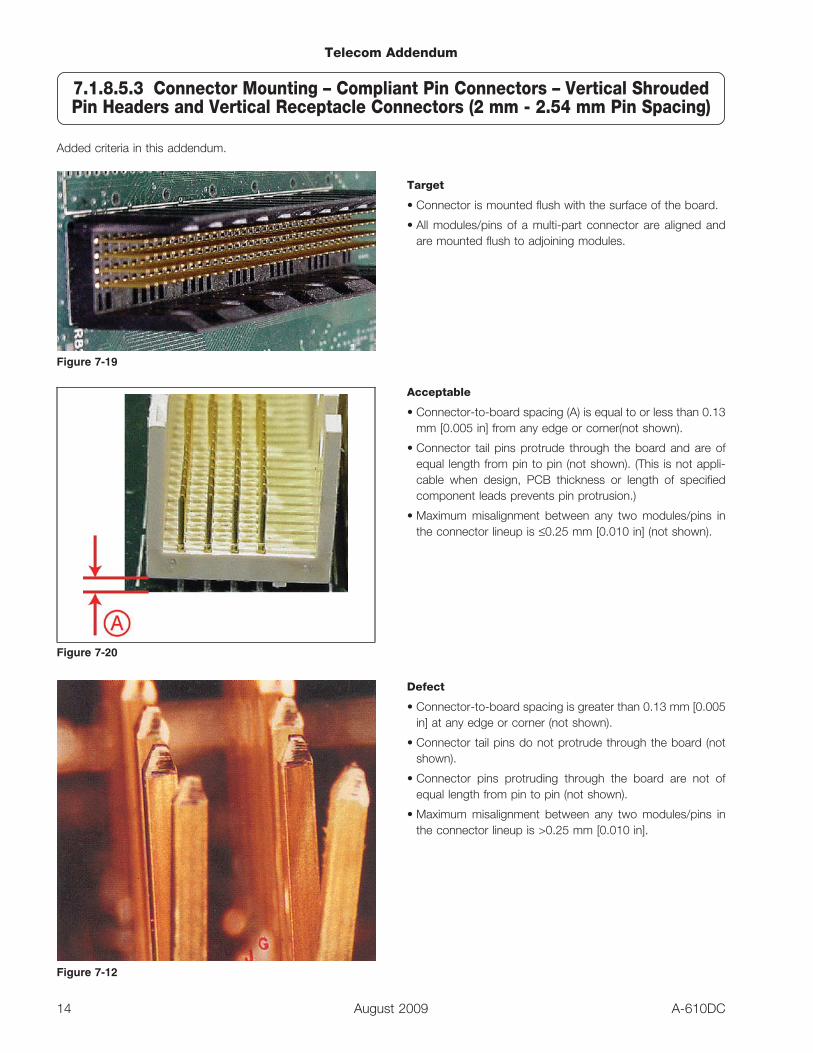
Added criteria in this addendum.
Target
• Connector is mounted flush with the surface of the board.
• All modules/pins of a multi-part connector are aligned andare mounted flush to adjoining modules.
Acceptable
• Connector-to-board spacing (A) is equal to or less than 0.13mm [0.005 in] from any edge or corner(not shown).
• Connector tail pins protrude through the board and are ofequal length from pin to pin (not shown). (This is not appli-cable when design, PCB thickness or length of specifiedcomponent leads prevents pin protrusion.)
• Maximum misalignment between any two modules/pins inthe connector lineup is ≤0.25 mm [0.010 in] (not shown).
Defect
• Connector-to-board spacing is greater than 0.13 mm [0.005in] at any edge or corner (not shown).
• Connector tail pins do not protrude through the board (notshown).
• Connector pins protruding through the board are not ofequal length from pin to pin (not shown).
• Maximum misalignment between any two modules/pins inthe connector lineup is >0.25 mm [0.010 in].
Figure 7-19
Figure 7-20
Figure 7-12
Telecom Addendum
7.1.8.5.3 Connector Mounting – Compliant Pin Connectors – Vertical ShroudedPin Headers and Vertical Receptacle Connectors (2 mm - 2.54 mm Pin Spacing)
14 A-610DCAugust 2009
Added criteria in this addendum.
There are no illustrations for these criteria.
Target
• Through-hole mounted LEDs are centered in the mountinghole.
• The tops of through-hole mounted LEDs protrude from thesurface of the panel.
Acceptable
• The tops of through-hole mounted LEDs are flush with thesurface of the panel.
• Three or more LEDs mounted in a row on a panel arealigned center to center and height.
Defect
• Front panel mounted LEDs are recessed below the surfaceof the panel.
Added criteria in this addendum.
Where a potential for shorting (violation of minimum electrical clearance) exists between conductive component bodies, at leastone of the bodies will be protected by an insulator.
These criteria replace all of 7.5.1 in published IPC-A-610D.
Defect
• Component height exceeds user-determined dimension (H).
• Components dissipating greater than 1 Watt are mountedless than 1.5 mm [0.059 in] above the board surface.
These criteria replace all of 7.5.5.1 in published IPC-A-610D.
Where large areas of copper (e.g., ground or power planes) or other heat sinks (e.g., heavy component leads) are connected toPTHs in PCBs, or where pin-in-paste processes are used on thick PCBs results in insufficient vertical solder fill and/or secondaryside land wetting, hole fill shall be sufficient to ensure that the minimum pin-wetted length within the barrel is at least .047 inchregardless of board thickness.
Telecom Addendum
7.1.10 Component Mounting – Front Panel Mounted LEDs
15A-610DC August 2009
7.1.11 Component Mounting – Conductive Cases
7.5.5.1 Supported Holes – Solder – Vertical fill (A)
7.5.1 Supported Holes – Axial Leaded – Horizontal
These criteria replace all of 7.5.5.7 in published IPC-A-610D.
Defect
• Does not meet requirements of Tables 7-6 or 7-7.
• Coating meniscus is in the plated through hole.
• Coating meniscus is embedded in the solder connection.
These criteria replace all of 8.2 in published IPC-A-610D.
SMT connections must meet the criteria of 8.2.1 through 8.2.14, as appropriate.
Where a potential for shorting (violation of minimum electrical clearance) exists between conductive component bodies, at leastone of the bodies will be protected by an insulator.
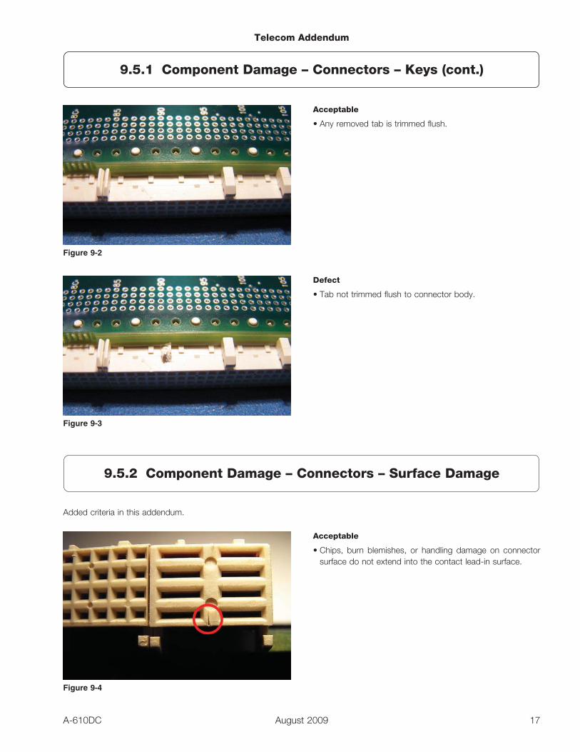
Added criteria in this addendum.
Acceptable
• Keying slots or holes are free of cracks, chips, or foreignmaterial that could interfere with the mating pin, blade, oralignment device (not shown).
Defect
• Keying slots or holes have cracks, chips, or foreign materialthat interferes with the mating pin, blade, or alignmentdevice (not shown).
Some connectors, e.g., FutureBus®, have key tabs wherekeys may be inserted. To prevent damage during handling ofthe finished circuit pack, it is permissible to remove the keytabs at the extreme ends of the connector line-up (A) after theconnectors are installed. In addition, a maximum of two (2)additional key tabs may be removed (if damaged during sub-sequent handling) provided that the following criteria are met:
• Broken tabs are trimmed flush to the connector body.
• Two (2) missing tabs are not next to each other on a givenmodule.
• Two (2) missing tabs are not the end tabs on adjacent con-nector modules (A).
• Tabs that secure required keys shall not be damaged.
Figure 9-1A. End tab key
Telecom Addendum
7.5.5.7 Supported Holes – Solder Conditions – Meniscus in Solder
16 A-610DCAugust 2009
8.2 SMT Connections
9.5.1 Component Damage – Connectors – Keys
Acceptable
• Any removed tab is trimmed flush.
Defect
• Tab not trimmed flush to connector body.
Added criteria in this addendum.
Acceptable
• Chips, burn blemishes, or handling damage on connectorsurface do not extend into the contact lead-in surface.
Figure 9-2
Figure 9-3
Figure 9-4
Telecom Addendum
9.5.1 Component Damage – Connectors – Keys (cont.)
17A-610DC August 2009
9.5.2 Component Damage – Connectors – Surface Damage
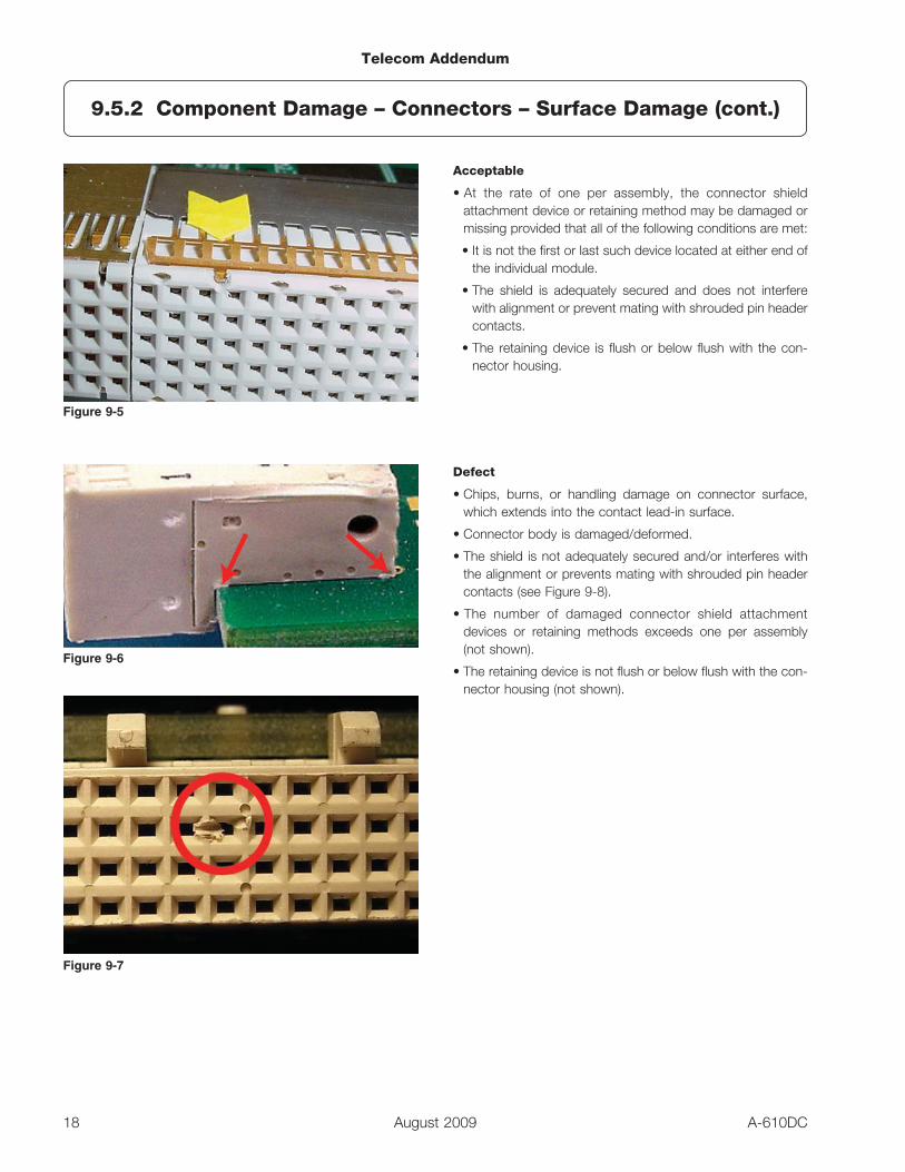
Acceptable
• At the rate of one per assembly, the connector shieldattachment device or retaining method may be damaged ormissing provided that all of the following conditions are met:
• It is not the first or last such device located at either end ofthe individual module.
• The shield is adequately secured and does not interferewith alignment or prevent mating with shrouded pin headercontacts.
• The retaining device is flush or below flush with the con-nector housing.
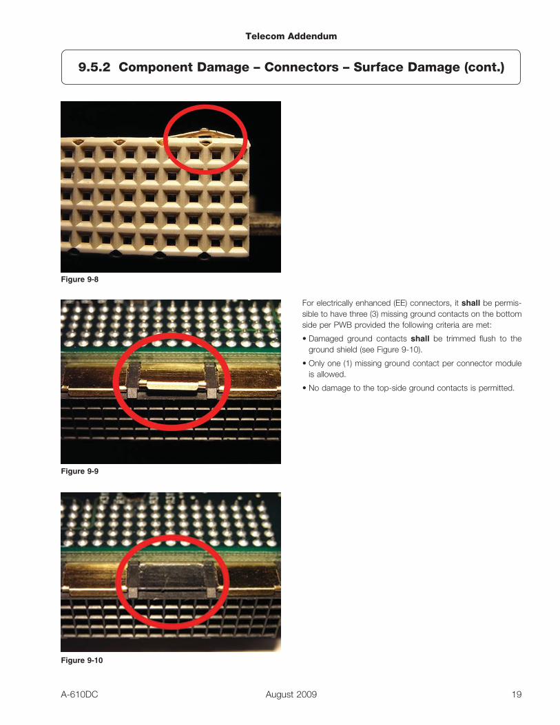
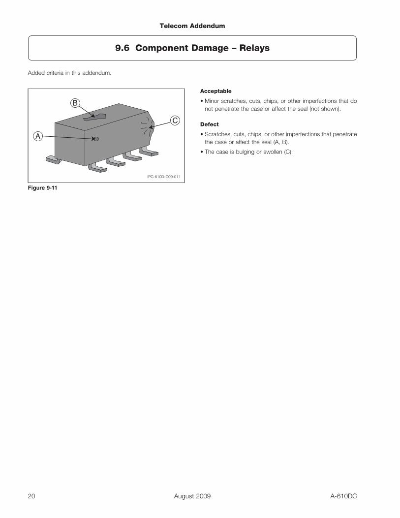
Defect
• Chips, burns, or handling damage on connector surface,which extends into the contact lead-in surface.
• Connector body is damaged/deformed.
• The shield is not adequately secured and/or interferes withthe alignment or prevents mating with shrouded pin headercontacts (see Figure 9-8).
• The number of damaged connector shield attachmentdevices or retaining methods exceeds one per assembly(not shown).
• The retaining device is not flush or below flush with the con-nector housing (not shown).
Figure 9-5
Figure 9-6
Figure 9-7
Telecom Addendum
9.5.2 Component Damage – Connectors – Surface Damage (cont.)
18 A-610DCAugust 2009
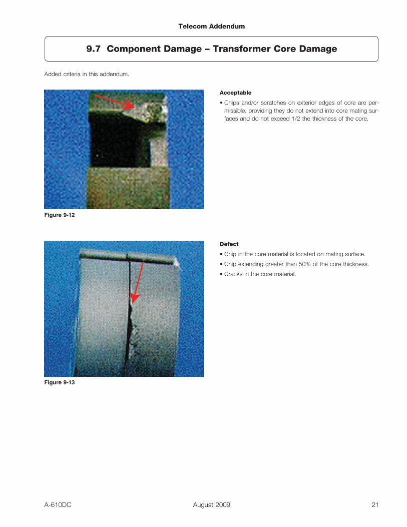
For electrically enhanced (EE) connectors, it shall be permis-sible to have three (3) missing ground contacts on the bottomside per PWB provided the following criteria are met:
• Damaged ground contacts shall be trimmed flush to theground shield (see Figure 9-10).
• Only one (1) missing ground contact per connector moduleis allowed.
• No damage to the top-side ground contacts is permitted.
Figure 9-8
Figure 9-9
Figure 9-10
Telecom Addendum
9.5.2 Component Damage – Connectors – Surface Damage (cont.)
19A-610DC August 2009
Added criteria in this addendum.
Acceptable
• Minor scratches, cuts, chips, or other imperfections that donot penetrate the case or affect the seal (not shown).
Defect
• Scratches, cuts, chips, or other imperfections that penetratethe case or affect the seal (A, B).
• The case is bulging or swollen (C).
IPC-610D-C09-011
Figure 9-11
C
B
A
Telecom Addendum
9.6 Component Damage – Relays
20 A-610DCAugust 2009
Added criteria in this addendum.
Acceptable
• Chips and/or scratches on exterior edges of core are per-missible, providing they do not extend into core mating sur-faces and do not exceed 1/2 the thickness of the core.
Defect
• Chip in the core material is located on mating surface.
• Chip extending greater than 50% of the core thickness.
• Cracks in the core material.
Figure 9-12
Figure 9-13
Telecom Addendum
9.7 Component Damage – Transformer Core Damage
21A-610DC August 2009
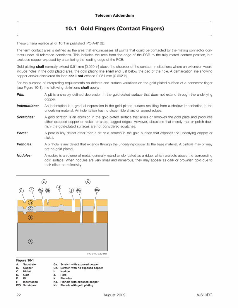
These criteria replace all of 10.1 in published IPC-A-610D.
The term contact area is defined as the area that encompasses all points that could be contacted by the mating connector con-tacts under all tolerance conditions. This includes the area from the edge of the PCB to the fully mated contact position, butexcludes copper exposed by chamfering the leading edge of the PCB.
Gold plating shall normally extend 0.51 mm [0.020 in] above the shoulder of the contact. In situations where an extension wouldinclude holes in the gold plated area, the gold plating line shall end just below the pad of the hole. A demarcation line showingcopper and/or discolored tin-lead shall not exceed 0.051 mm [0.002 in].
For the purpose of interpreting requirements on defects and surface variations on the gold-plated surface of a connector finger(see Figure 10-1), the following definitions shall apply:
Pits: A pit is a sharply defined depression in the gold-plated surface that does not extend through the underlyingcopper.
Indentations: An indentation is a gradual depression in the gold-plated surface resulting from a shallow imperfection in theunderlying material. An indentation has no discernible sharp or jagged edges.
Scratches: A gold scratch is an abrasion in the gold-plated surface that alters or removes the gold plate and produceseither exposed copper or nickel, or sharp, jagged edges. However, abrasions that merely mar or polish (bur-nish) the gold-plated surfaces are not considered scratches.
Pores: A pore is any defect other than a pit or a scratch in the gold surface that exposes the underlying copper ornickel.
Pinholes: A pinhole is any defect that extends through the underlying copper to the base material. A pinhole may or maynot be gold plated.
Nodules: A nodule is a volume of metal, generally round or elongated as a ridge, which projects above the surroundinggold surface. When nodules are very small and numerous, they may appear as dark or brownish gold due totheir effect on reflectivity.
IPC-610D-C10-001
Figure 10-1A. SubstrateB. CopperC. NickelD. GoldE. PitF. IndentationE/G. Scratches
Ga. Scratch with exposed copperGb. Scratch with no exposed copperH. NoduleJ. PoreK. PinholesKa. Pinhole with exposed copperKb. Pinhole with gold plating
A
B
C
D
E F
G
Ga GbH
J Ka Kb
K
Telecom Addendum
10.1 Gold Fingers (Contact Fingers)
22 A-610DCAugust 2009
Nickel, gold, or other contact metal plating, shall not be applied over solder on contact fingers.
Contact plating on circuits and vias in the demarcation area is not cause for rejection.
Solder spots, smears, or other contaminates, visible with 1.75X magnification are not acceptable. 4X magnification may be usedfor referee purposes.
Isolated conditions, including but not limited to indentations, nicks, scratches or pits in the contact area of gold fingers, shall notexpose base metal or under-plate.
Minor test probe indentations are acceptable provided the laminate, copper or nickel is not exposed and their maximum diameterdoes not exceed 0.25 mm [0.010 in].
No more than 5% of the finger width of an edge board contact may be removed when drilled holes are used to remove platingbars between gold fingers. Loss of adhesion of the metallization or residual burrs is not acceptable.
Repair of gold plating shall meet all requirements of this specification.
Replacement of gold fingers is not allowed.
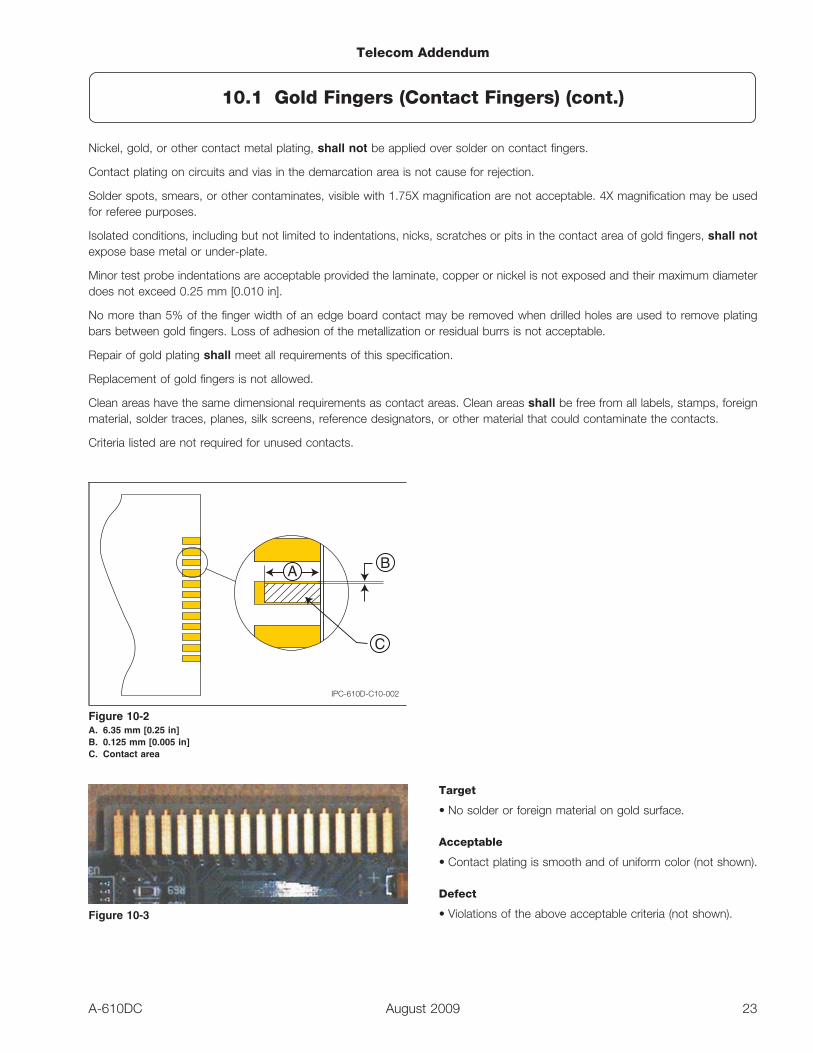
Clean areas have the same dimensional requirements as contact areas. Clean areas shall be free from all labels, stamps, foreignmaterial, solder traces, planes, silk screens, reference designators, or other material that could contaminate the contacts.
Criteria listed are not required for unused contacts.
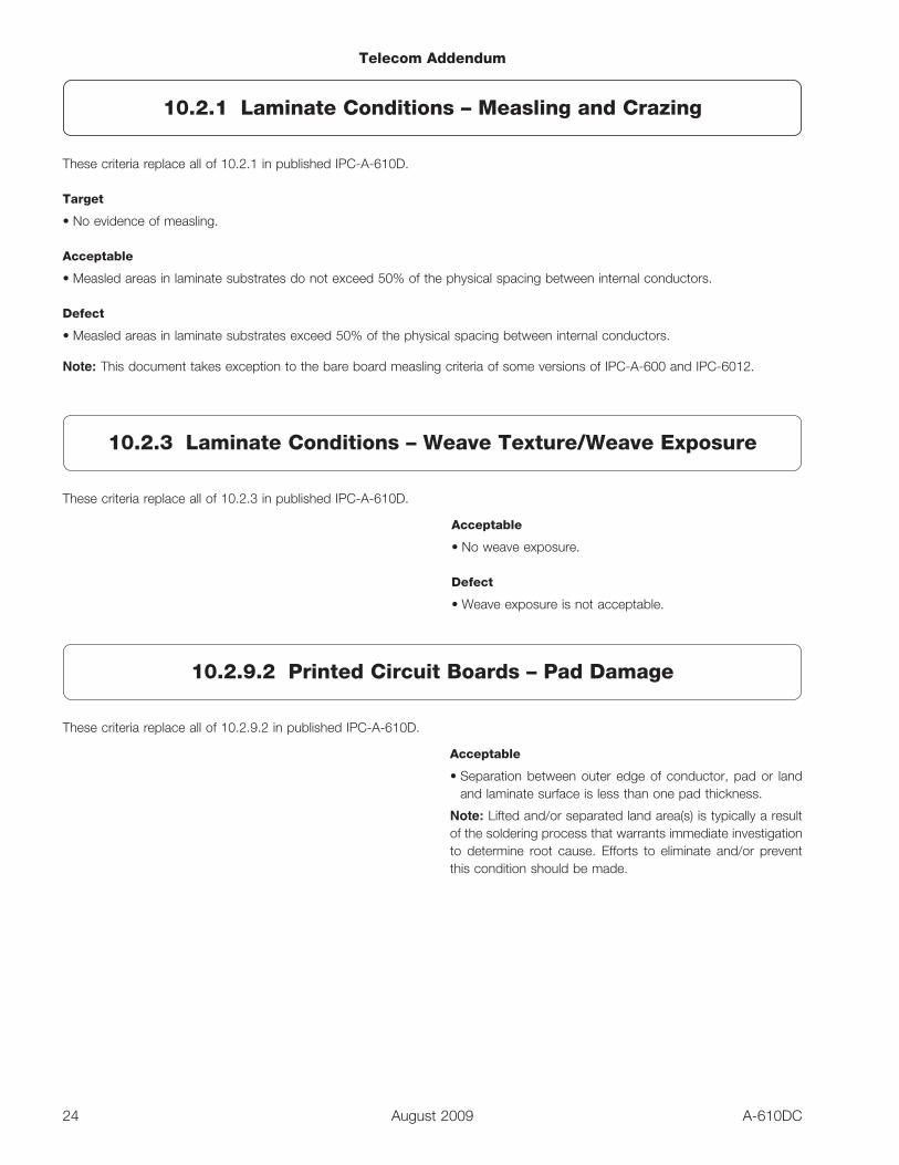
Target
• No solder or foreign material on gold surface.
Acceptable
• Contact plating is smooth and of uniform color (not shown).
Defect
• Violations of the above acceptable criteria (not shown).
IPC-610D-C10-002
Figure 10-2A. 6.35 mm [0.25 in]B. 0.125 mm [0.005 in]C. Contact area
A B
C
Figure 10-3
Telecom Addendum
10.1 Gold Fingers (Contact Fingers) (cont.)
23A-610DC August 2009
These criteria replace all of 10.2.1 in published IPC-A-610D.
Target
• No evidence of measling.
Acceptable
• Measled areas in laminate substrates do not exceed 50% of the physical spacing between internal conductors.
Defect
• Measled areas in laminate substrates exceed 50% of the physical spacing between internal conductors.
Note: This document takes exception to the bare board measling criteria of some versions of IPC-A-600 and IPC-6012.
These criteria replace all of 10.2.3 in published IPC-A-610D.
Acceptable
• No weave exposure.
Defect
• Weave exposure is not acceptable.
These criteria replace all of 10.2.9.2 in published IPC-A-610D.
Acceptable
• Separation between outer edge of conductor, pad or landand laminate surface is less than one pad thickness.
Note: Lifted and/or separated land area(s) is typically a resultof the soldering process that warrants immediate investigationto determine root cause. Efforts to eliminate and/or preventthis condition should be made.
Telecom Addendum
10.2.1 Laminate Conditions – Measling and Crazing
24 A-610DCAugust 2009
10.2.3 Laminate Conditions – Weave Texture/Weave Exposure
10.2.9.2 Printed Circuit Boards – Pad Damage
These criteria replace all of 10.3 in published IPC-A-610D.
Acceptable
• Required marking is present.
• Marking is legible at a viewing distance of 460 mm [18 in].
Defect
• Required marking is not present.
• Marking is not legible.
• Marking cannot be read at a viewing distance of 460 mm[18 in].
These criteria replace all of 10.3.3 in published IPC-A-610D.
Acceptable
• Lines of a number or letter may be broken (or the ink thinover a portion of the character) providing the breaks do notmake the markings illegible.
• The open areas within characters may be filled providing thecharacters are legible, i.e., cannot be confused with anotherletter or number.
Defect
• Marking ink is present on the land interfering with the solderrequirements of Tables 7-3, 7-6 or 7-7 or with the surfacemount soldering requirements of Section 8.
• Marking inks form a conductive path that violates minimumelectrical clearance.
Acceptable
• Marking that has been smeared or blurred but is still legible.
• Double stamped markings are acceptable provided the gen-eral intent can be determined.
• Missing or smeared marking does not exceed 10% of thecharacter and the character is still legible.
Note: Acceptance stamp impressions do not need to be leg-ible as long as the intent of the stamp can be determined andthe operation/approval is recorded electronically.
Telecom Addendum
10.3 Marking
25A-610DC August 2009
10.3.3 Marking – Stamped

These criteria replace all of 10.3.5.3 in published IPC-A-610D.
Acceptable
• Adhesion is complete, shows no sign of damage or peeling.
Defect
• Label is peeling.
• Missing labels.
• Label wrinkle affects readability.
• Labels are not positioned according to engineering docu-mentation or labels that are not consistent, square, parallel,or centered.
• Labels are not readable in the finished assembly.
• Labels or markings obscure other markings or identifica-tions.
• Labels or markings damage the underlying surface, createconductive paths, or affect the utility of the product.
• Labels are placed in areas where they are susceptible todamage.
• Wrap-around cable labels do not wrap completely aroundthe cable.
• Wrap-around labels where the clear over-wrap portion doesnot completely cover the markings.
• Cable marking bands create a safety hazard (burrs, sharpedges) or a potential for electrical shorts.
• Tie-on labels are held in place with conductive materials.
• Tie-on labels restrict access or visibility to marking informa-tion or cause problems with entanglement with otherassemblies.
• Labels replaced by putting one label on top of another.
Figure 10-5
Figure 10-6
Figure 10-4
Telecom Addendum
10.3.5.3 Marking – Labels – Adhesion and Damage
26 A-610DCAugust 2009
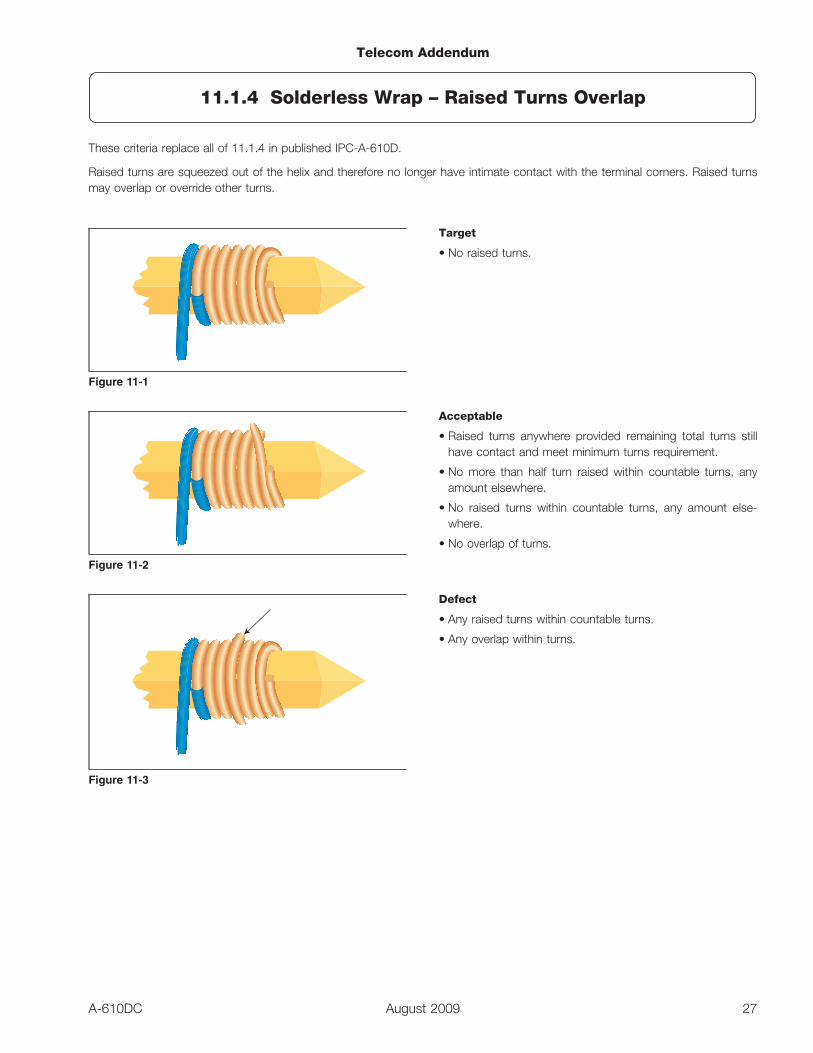
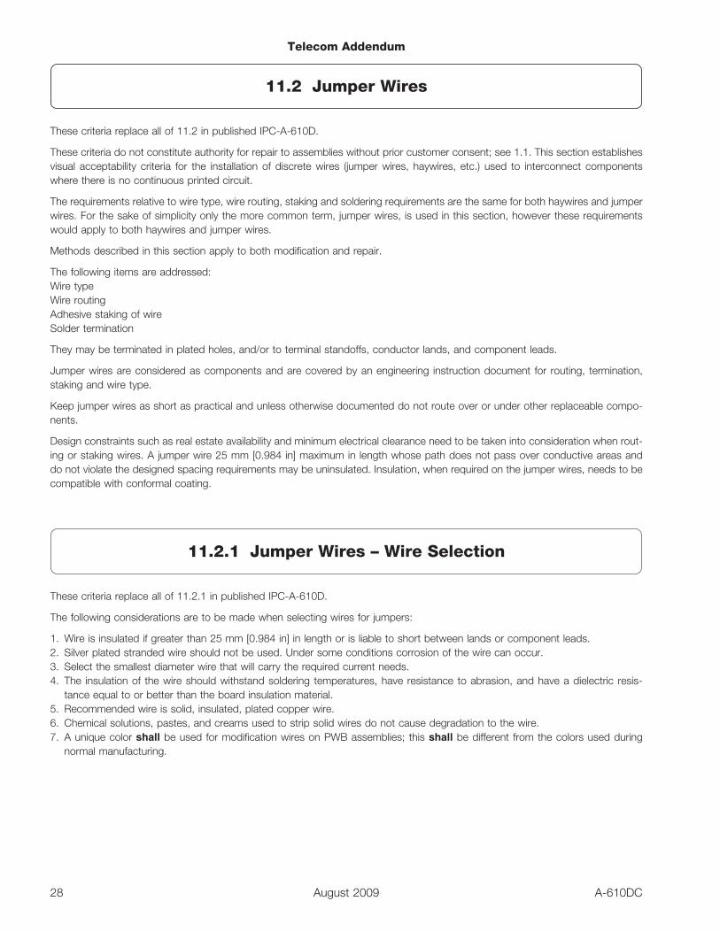
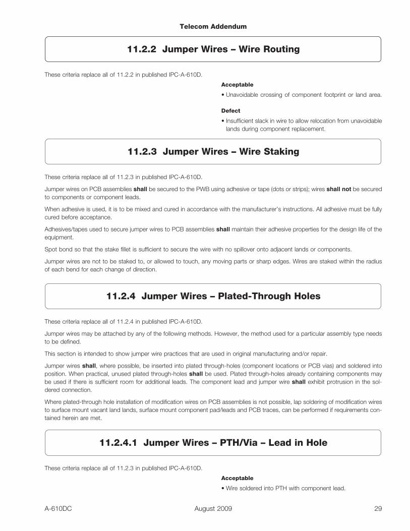
These criteria replace all of 11.1.4 in published IPC-A-610D.
Raised turns are squeezed out of the helix and therefore no longer have intimate contact with the terminal corners. Raised turnsmay overlap or override other turns.
Target
• No raised turns.
Acceptable
• Raised turns anywhere provided remaining total turns stillhave contact and meet minimum turns requirement.
• No more than half turn raised within countable turns, anyamount elsewhere.
• No raised turns within countable turns, any amount else-where.
• No overlap of turns.
Defect
• Any raised turns within countable turns.
• Any overlap within turns.
Figure 11-1
Figure 11-2
Figure 11-3
Telecom Addendum
11.1.4 Solderless Wrap – Raised Turns Overlap
27A-610DC August 2009
These criteria replace all of 11.2 in published IPC-A-610D.
These criteria do not constitute authority for repair to assemblies without prior customer consent; see 1.1. This section establishesvisual acceptability criteria for the installation of discrete wires (jumper wires, haywires, etc.) used to interconnect componentswhere there is no continuous printed circuit.
The requirements relative to wire type, wire routing, staking and soldering requirements are the same for both haywires and jumperwires. For the sake of simplicity only the more common term, jumper wires, is used in this section, however these requirementswould apply to both haywires and jumper wires.
Methods described in this section apply to both modification and repair.
The following items are addressed:Wire typeWire routingAdhesive staking of wireSolder termination
They may be terminated in plated holes, and/or to terminal standoffs, conductor lands, and component leads.
Jumper wires are considered as components and are covered by an engineering instruction document for routing, termination,staking and wire type.
Keep jumper wires as short as practical and unless otherwise documented do not route over or under other replaceable compo-nents.
Design constraints such as real estate availability and minimum electrical clearance need to be taken into consideration when rout-ing or staking wires. A jumper wire 25 mm [0.984 in] maximum in length whose path does not pass over conductive areas anddo not violate the designed spacing requirements may be uninsulated. Insulation, when required on the jumper wires, needs to becompatible with conformal coating.
These criteria replace all of 11.2.1 in published IPC-A-610D.
The following considerations are to be made when selecting wires for jumpers:
1. Wire is insulated if greater than 25 mm [0.984 in] in length or is liable to short between lands or component leads.2. Silver plated stranded wire should not be used. Under some conditions corrosion of the wire can occur.3. Select the smallest diameter wire that will carry the required current needs.4. The insulation of the wire should withstand soldering temperatures, have resistance to abrasion, and have a dielectric resis-
tance equal to or better than the board insulation material.5. Recommended wire is solid, insulated, plated copper wire.6. Chemical solutions, pastes, and creams used to strip solid wires do not cause degradation to the wire.7. A unique color shall be used for modification wires on PWB assemblies; this shall be different from the colors used during
normal manufacturing.
Telecom Addendum
11.2 Jumper Wires
28 A-610DCAugust 2009
11.2.1 Jumper Wires – Wire Selection
These criteria replace all of 11.2.2 in published IPC-A-610D.
Acceptable
• Unavoidable crossing of component footprint or land area.
Defect
• Insufficient slack in wire to allow relocation from unavoidablelands during component replacement.
These criteria replace all of 11.2.3 in published IPC-A-610D.
Jumper wires on PCB assemblies shall be secured to the PWB using adhesive or tape (dots or strips); wires shall not be securedto components or component leads.
When adhesive is used, it is to be mixed and cured in accordance with the manufacturer’s instructions. All adhesive must be fullycured before acceptance.
Adhesives/tapes used to secure jumper wires to PCB assemblies shall maintain their adhesive properties for the design life of theequipment.
Spot bond so that the stake fillet is sufficient to secure the wire with no spillover onto adjacent lands or components.
Jumper wires are not to be staked to, or allowed to touch, any moving parts or sharp edges. Wires are staked within the radiusof each bend for each change of direction.
These criteria replace all of 11.2.4 in published IPC-A-610D.
Jumper wires may be attached by any of the following methods. However, the method used for a particular assembly type needsto be defined.
This section is intended to show jumper wire practices that are used in original manufacturing and/or repair.
Jumper wires shall, where possible, be inserted into plated through-holes (component locations or PCB vias) and soldered intoposition. When practical, unused plated through-holes shall be used. Plated through-holes already containing components maybe used if there is sufficient room for additional leads. The component lead and jumper wire shall exhibit protrusion in the sol-dered connection.
Where plated-through hole installation of modification wires on PCB assemblies is not possible, lap soldering of modification wiresto surface mount vacant land lands, surface mount component pad/leads and PCB traces, can be performed if requirements con-tained herein are met.
These criteria replace all of 11.2.3 in published IPC-A-610D.
Acceptable
• Wire soldered into PTH with component lead.
Telecom Addendum
11.2.2 Jumper Wires – Wire Routing
29A-610DC August 2009
11.2.3 Jumper Wires – Wire Staking
11.2.4.1 Jumper Wires – PTH/Via – Lead in Hole
11.2.4 Jumper Wires – Plated-Through Holes
Added criteria in this addendum.
All individual cables and cable harness assemblies shall contain the part number, revision level, date code (date of manufacturer),and supplier identification (name, abbreviation, or number).
Supplier lot control numbers/date codes shall be marked on cables and harnesses.
The component manufacturer’s recommended tooling and processes shall be used in all preparation and assembly operations.
Splicing is not permitted.
Added criteria in this addendum.
Modifications:Modifications are defined as the alteration of printed circuit boards (PCBs) to incorporate approved engineering changes. ModifiedPCBs shall be clearly identified (e.g., raising revision level or variant) to avoid confusion with unmodified product. Before begin-ning any modifications, engineering shall provide documented & released process instructions.
Repairs:Conductor short repairs (cut/drilled traces, etc.) shall be limited to a maximum of six per PWB, provided a qualified polymericcoating is subsequently applied to the affected area. Repairs to outer layer conductors of PWBs for open circuits (added wires,welded conductors, etc.), shall not exceed five for a single cause (such as a single scratch through up to five adjacent conduc-tors); however, the limit is one, solitary defect per 0.064 square meters [100 square in]. For boards of less than 0.064 squaremeters [100 square in], five repairs for a single defect cause are permitted.
SUBTRACTIVE MODIFICATIONS/REPAIRS
Cut Traces:• The width of all circuit trace cuts shall exceed 0.063 mm [0.005 in].
• All loose material shall be removed from the cut area.
• Circuit trace cuts shall be sealed with an approved epoxy.
• Removed circuit traces must be a minimum of 0.063 mm [0.005 in] from lands, circuit junctions, and component leads.
Holes and Terminals:Holes may be drilled in boards to add terminals, to route added wires, or to interrupt internal circuits providing the following con-ditions are met:
• The drilled hole does not interfere with other circuits.
• There is no smeared metallization that could short ground and power planes on multi-layer boards.
• Holes to interrupt internal circuits and holes penetrating more than one conductive layer must be filled with epoxy to preventabsorption of moisture or other contaminants.
• The edge of the drilled hole shall be a minimum of 0.38 mm [0.015 in] away from any adjacent hole, pad, internal PTH (PlatedThrough-Hole) clearance diameter, etc.
• Excess, mislocated or unused holes or slots in boards may be filled with an approved epoxy.
Lifted/Cut Component Leads:• Lifted (truncated) pins shall be cut short enough to prevent shorting to the pad from which they were lifted.
• Minimum electrical clearance requirements shall be maintained.
Telecom Addendum
13 Wiring and Cabling – General Requirements
30 A-610DCAugust 2009
14 Modification and Repair
COMPONENT ADDITIONS
Leaded Components• Connections must be supported, preferably by existing terminals or PTH. Terminals may be added as the case dictates.
• Added components shall be soldered into plated through-holes (component locations or PCB vias). Added components shallbe mounted on the same side of the PCB as the original mounted component.
• Butt mounting of axial leaded components is prohibited.
• Components not reasonably secure shall have epoxy applied between the body and PCB surface.
SMT ComponentsSurface mounted components shall be added only where lands are provided. The use of additional adapter board supported SMTlands is permitted to replace damaged lands or to incorporate approved engineering changes. SMT pad size and configurationshall be as specified for the component.
CONDUCTOR REPAIR
General RequirementsThe following repair methods may be used to repair conductor breaks, scratches, or similar defects; see Section 11.2 conductorrepair.
Lifted or debonded circuit traces may be replaced with lap-soldered jumper wires. PTHs, lands, and vias shall be used whereverpossible. Wires may be lap-soldered to circuit traces if PTHs, lands, or vias are not available.
Jumper wire size, spacing, and current carrying capacity must not be reduced below allowable tolerance or electrical requirements.
Jumper wire size shall not exceed the width of the defective circuit trace.
Added criteria in this addendum.
The following classifications are to be used for inspection of finished surfaces unless workmanship requirements are specified onthe released engineering drawing.
Note: The terms Grade 1, Grade 2 and Grade 3 correspond to terms commonly used in the Telecom industry Class 1, Class 2and Class 3 where Grade 1/Class 1 are the most stringent requirements. In IPC documents the terms Class 1, 2, or 3 are usedto reflect criticality of need and ability to operate in harsh environmental conditions (thermal, vibration, etc.) where Class 3 are themost stringent requirements. In this addendum the committee chose to use the designation ‘‘Grade’’ instead of ‘‘Class’’ to reduceconfusion with the Class designations used in all IPC documents.
Grade 1 Surfaces
• Surfaces frequently viewed in the finished product by the final customer (Examples: Front covers, module covers, faceplates, fillerpanels, heat ramps, external labels, etc.).
• Grade 1 surfaces shall be free of blisters, clamp or brake marks, extrusion lines, gouges, nicks, pits, runs, scratches, extrane-ous or irregular sanding lines, spot-weld craters, voids, or other defects which detract from the general appearance.
• Appearance of a grade 1 surface is as important as form, fit, and function.
Grade 2 Surfaces
• Surfaces occasionally viewed in the finished product by the final customer (Examples: Internal labels and surrounding area, insideof accessible covers, side panels visible from the front, outside of rear covers, outdoor equipment enclosures, etc.).
• Grade 2 surfaces may have slight surface imperfections/scratches if they are not readily noticeable from a distance of 18 inches.
• Appearance of a grade 2 surface, while important, is secondary to form, fit, and function.
• Consideration should be given to how the flaw affects the general appearance.
Telecom Addendum
14 Modification and Repair (cont.)
31A-610DC August 2009
15 Finished Surfaces
Grade 3 Surfaces
• Surfaces infrequently or never viewed in the finished product by the final customer (Examples: Normally concealed surfaces, bot-tom plates, top plates, internal surfaces of assemblies, etc.).
• Grade 3 surfaces are allowed to have a limited number of minor flaws that would be considered non-conforming in Grade 1 and2 as long as form, fit, and function of the part are not affected.
• Scratches that are visible at a distance of 457 mm [18.0 in] are allowed providing the scratch does not expose the base mate-rial.
• Form, fit, and function are the primary considerations when evaluating a grade 3 surface.
Evaluation Requirements
When evaluating a flaw, consider whether the flaw adversely affects the general appearance, based on the quality requirementsfor the surface exposure classification.
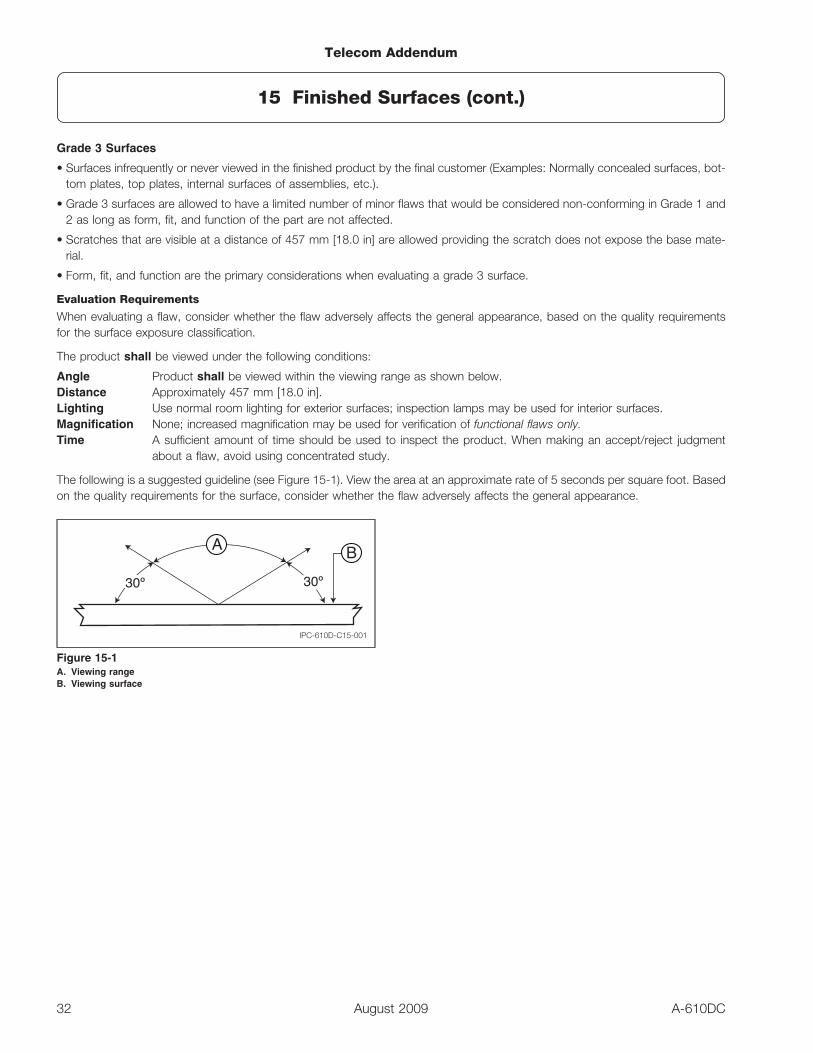
The product shall be viewed under the following conditions:
Angle Product shall be viewed within the viewing range as shown below.Distance Approximately 457 mm [18.0 in].Lighting Use normal room lighting for exterior surfaces; inspection lamps may be used for interior surfaces.Magnification None; increased magnification may be used for verification of functional flaws only.Time A sufficient amount of time should be used to inspect the product. When making an accept/reject judgment
about a flaw, avoid using concentrated study.
The following is a suggested guideline (see Figure 15-1). View the area at an approximate rate of 5 seconds per square foot. Basedon the quality requirements for the surface, consider whether the flaw adversely affects the general appearance.
A
30º 30º
B
IPC-610D-C15-001
Figure 15-1A. Viewing rangeB. Viewing surface
Telecom Addendum
15 Finished Surfaces (cont.)
32 A-610DCAugust 2009
Added criteria in this addendum.
Target
• Cosmetic and protective finishes shall be of uniformappearance and typically smooth; deliberately textured fin-ishes are permissible when directed by engineering docu-mentation.
• Finishes shall conform to environmental conditions andrestrictions as delineated in engineering documentation. Fin-ishes shall also be resistant to cleaning agents or othermanufacturing processes and shall not functionallydegrade over the expected life of the product.
• All finishes, regardless of class, shall provide the intendedcorrosion protection. Exposed base material is a defect inany finish class.
• Touch-up of finishes on all grades is allowed. Completedtouch-up areas shall meet the requirements of the appro-priate finish grade.
Acceptable
• See specific finish sections for detailed criteria on accept-able finishes.
Defect
• Flaws on mechanical assembly component parts, that mayin any way endanger the safety of persons using or comingin contact with these parts, are always considered defects.
• Flaws that affect the form, fit, or function of a part or theproduct, regardless of surface exposure classification, arealways considered defects.
• There shall be no evidence of bleed-out or corrosion due toentrapment of plating or cleaning solutions.
• See specific finish sections for detailed criteria on defect fin-ishes.
Telecom Addendum
15.1 General Finish Requirements and Acceptance Criteria
33A-610DC August 2009
Added criteria in this addendum.
Adhesion Tape Test
• Adhesion of chromated surfaces shall be determined by the following adhesion tape test. A new strip of tape shall be used foreach test.
• A two inch minimum effective length of pressure sensitive tape conforming to the requirements of Federal Specification PPP-T-42C, Type II (such as 3M Flatback Tape #250™) shall be firmly pressed onto the surface to be tested.
• All air bubbles should be rubbed out.
• Allow approximately 10 seconds for the test area to return to room temperature.
• Grasp a free end of the tape and at a rapid speed, strip it by pulling the tape back on itself at 90- 180° so that the tape is foldedback to back during the procedure.
Acceptable
• No presence of chromate coating on the removed tape.
Defect
• Any chromate coating present on the removed tape.
Adhesion Tape Test
• Ink shall have sufficient adhesion to withstand the following adhesion tape test. A new strip of tape shall be used for each test.
• Flatback™ masking tape conforming to the requirements of Federal Specification PPP-T-42C, Type II (Minnesota Mining andManufacturing Company, No. 250) and of sufficient width to cover the characters shall be used.
• Press a strip of the tape approximately 50.8 mm [2 in] long firmly across the silkscreen ink surface and substrate.
• Immediately remove a short length of one end of the applied tape and then rapidly remove the tape by manual force applied 90- 180° to the ink marking.
TargetAcceptable
• No presence of ink on the removed tape.
Defect
• Any portion of ink markings present on the removed tape.
Added criteria in this addendum.
Requirements for physical defects and finish defects are in Tables 15-1 and 15-2.
Telecom Addendum
15.2 Adhesion Requirements for Chromated Surfaces
34 A-610DCAugust 2009
15.3 Adhesion Requirements for Silkscreen Ink
15.4 General Requirements for All Surfaces
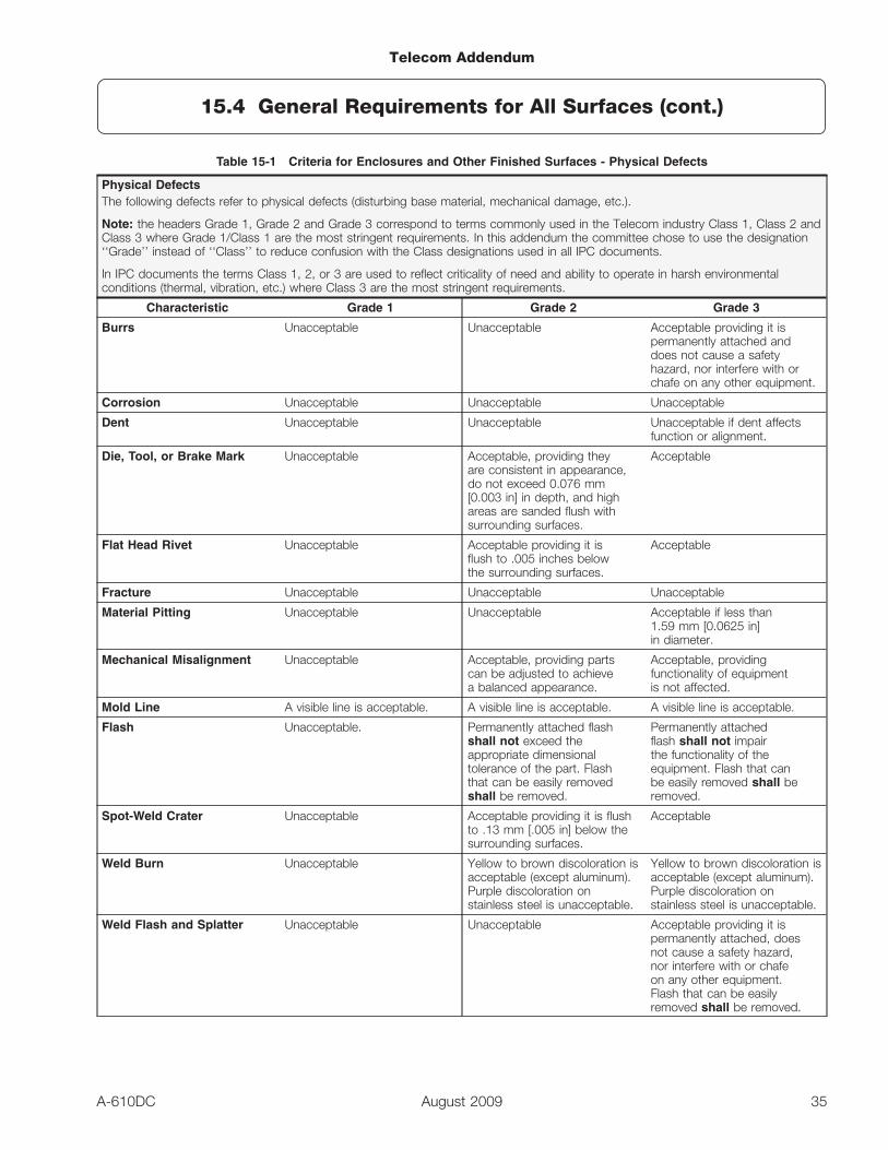
Table 15-1 Criteria for Enclosures and Other Finished Surfaces - Physical Defects
Physical DefectsThe following defects refer to physical defects (disturbing base material, mechanical damage, etc.).
Note: the headers Grade 1, Grade 2 and Grade 3 correspond to terms commonly used in the Telecom industry Class 1, Class 2 andClass 3 where Grade 1/Class 1 are the most stringent requirements. In this addendum the committee chose to use the designation‘‘Grade’’ instead of ‘‘Class’’ to reduce confusion with the Class designations used in all IPC documents.
In IPC documents the terms Class 1, 2, or 3 are used to reflect criticality of need and ability to operate in harsh environmentalconditions (thermal, vibration, etc.) where Class 3 are the most stringent requirements.
Characteristic Grade 1 Grade 2 Grade 3
Burrs Unacceptable Unacceptable Acceptable providing it ispermanently attached anddoes not cause a safetyhazard, nor interfere with orchafe on any other equipment.
Corrosion Unacceptable Unacceptable Unacceptable
Dent Unacceptable Unacceptable Unacceptable if dent affectsfunction or alignment.
Die, Tool, or Brake Mark Unacceptable Acceptable, providing theyare consistent in appearance,do not exceed 0.076 mm[0.003 in] in depth, and highareas are sanded flush withsurrounding surfaces.
Acceptable
Flat Head Rivet Unacceptable Acceptable providing it isflush to .005 inches belowthe surrounding surfaces.
Acceptable
Fracture Unacceptable Unacceptable Unacceptable
Material Pitting Unacceptable Unacceptable Acceptable if less than1.59 mm [0.0625 in]in diameter.
Mechanical Misalignment Unacceptable Acceptable, providing partscan be adjusted to achievea balanced appearance.
Acceptable, providingfunctionality of equipmentis not affected.
Mold Line A visible line is acceptable. A visible line is acceptable. A visible line is acceptable.
Flash Unacceptable. Permanently attached flashshall not exceed theappropriate dimensionaltolerance of the part. Flashthat can be easily removedshall be removed.
Permanently attachedflash shall not impairthe functionality of theequipment. Flash that canbe easily removed shall beremoved.
Spot-Weld Crater Unacceptable Acceptable providing it is flushto .13 mm [.005 in] below thesurrounding surfaces.
Acceptable
Weld Burn Unacceptable Yellow to brown discoloration isacceptable (except aluminum).Purple discoloration onstainless steel is unacceptable.
Yellow to brown discoloration isacceptable (except aluminum).Purple discoloration onstainless steel is unacceptable.
Weld Flash and Splatter Unacceptable Unacceptable Acceptable providing it ispermanently attached, doesnot cause a safety hazard,nor interfere with or chafeon any other equipment.Flash that can be easilyremoved shall be removed.
Telecom Addendum
15.4 General Requirements for All Surfaces (cont.)
35A-610DC August 2009
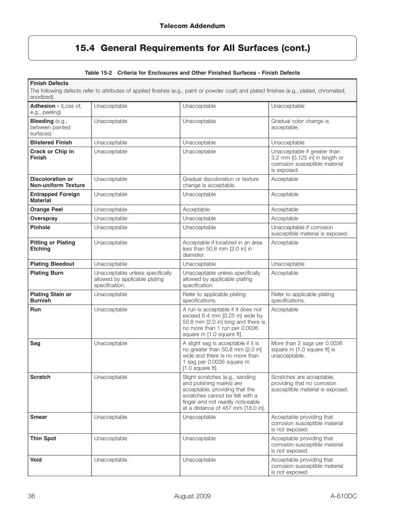
Table 15-2 Criteria for Enclosures and Other Finished Surfaces - Finish Defects
Finish DefectsThe following defects refer to attributes of applied finishes (e.g., paint or powder coat) and plated finishes (e.g., plated, chromated,anodized).
Adhesion - (Loss of,e.g., peeling)
Unacceptable Unacceptable Unacceptable
Bleeding (e.g.,between paintedsurfaces)
Unacceptable Unacceptable Gradual color change isacceptable.
Blistered Finish Unacceptable Unacceptable Unacceptable
Crack or Chip inFinish
Unacceptable Unacceptable Unacceptable if greater than3.2 mm [0.125 in] in length orcorrosion susceptible materialis exposed.
Discoloration orNon-uniform Texture
Unacceptable Gradual discoloration or texturechange is acceptable.
Acceptable
Entrapped ForeignMaterial
Unacceptable Unacceptable Acceptable
Orange Peel Unacceptable Acceptable Acceptable
Overspray Unacceptable Unacceptable Acceptable
Pinhole Unacceptable Unacceptable Unacceptable if corrosionsusceptible material is exposed.
Pitting or PlatingEtching
Unacceptable Acceptable if localized in an arealess than 50.8 mm [2.0 in] indiameter.
Acceptable
Plating Bleedout Unacceptable Unacceptable Unacceptable
Plating Burn Unacceptable unless specificallyallowed by applicable platingspecification.
Unacceptable unless specificallyallowed by applicable platingspecification.
Acceptable
Plating Stain orBurnish
Unacceptable Refer to applicable platingspecifications.
Refer to applicable platingspecifications.
Run Unacceptable A run is acceptable if it does notexceed 6.4 mm [0.25 in] wide by50.8 mm [2.0 in] long and there isno more than 1 run per 0.0036square m [1.0 square ft].
Acceptable
Sag Unacceptable A slight sag is acceptable if it isno greater than 50.8 mm [2.0 in]wide and there is no more than1 sag per 0.0036 square m[1.0 square ft].
More than 2 sags per 0.0036square m [1.0 square ft] isunacceptable.
Scratch Unacceptable Slight scratches (e.g., sandingand polishing marks) areacceptable, providing that thescratches cannot be felt with afinger and not readily noticeableat a distance of 457 mm [18.0 in].
Scratches are acceptable,providing that no corrosionsusceptible material is exposed.
Smear Unacceptable Unacceptable Acceptable providing thatcorrosion susceptible materialis not exposed.
Thin Spot Unacceptable Unacceptable Acceptable providing thatcorrosion susceptible materialis not exposed.
Void Unacceptable Unacceptable Acceptable providing thatcorrosion susceptible materialis not exposed.
Telecom Addendum
15.4 General Requirements for All Surfaces (cont.)
36 A-610DCAugust 2009
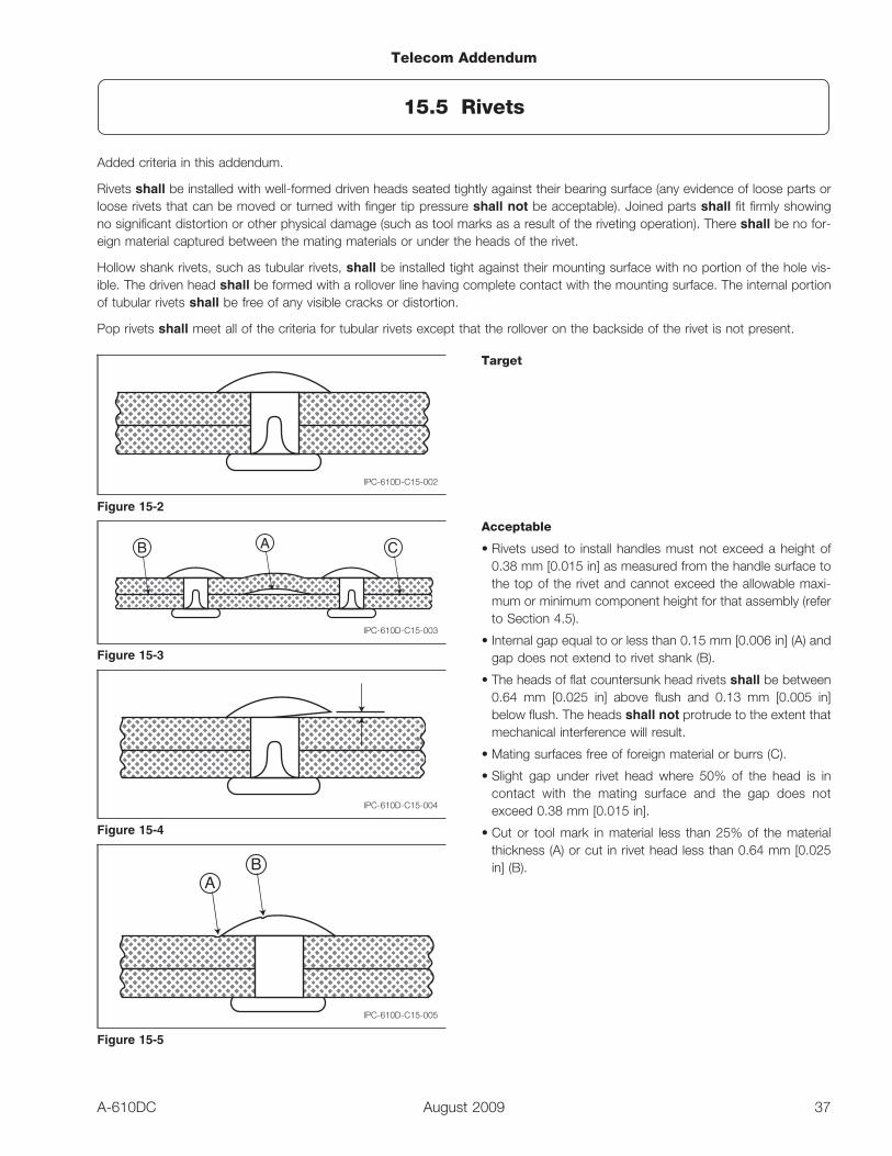
Added criteria in this addendum.
Rivets shall be installed with well-formed driven heads seated tightly against their bearing surface (any evidence of loose parts orloose rivets that can be moved or turned with finger tip pressure shall not be acceptable). Joined parts shall fit firmly showingno significant distortion or other physical damage (such as tool marks as a result of the riveting operation). There shall be no for-eign material captured between the mating materials or under the heads of the rivet.
Hollow shank rivets, such as tubular rivets, shall be installed tight against their mounting surface with no portion of the hole vis-ible. The driven head shall be formed with a rollover line having complete contact with the mounting surface. The internal portionof tubular rivets shall be free of any visible cracks or distortion.
Pop rivets shall meet all of the criteria for tubular rivets except that the rollover on the backside of the rivet is not present.
Target
Acceptable
• Rivets used to install handles must not exceed a height of0.38 mm [0.015 in] as measured from the handle surface tothe top of the rivet and cannot exceed the allowable maxi-mum or minimum component height for that assembly (referto Section 4.5).
• Internal gap equal to or less than 0.15 mm [0.006 in] (A) andgap does not extend to rivet shank (B).
• The heads of flat countersunk head rivets shall be between0.64 mm [0.025 in] above flush and 0.13 mm [0.005 in]below flush. The heads shall not protrude to the extent thatmechanical interference will result.
• Mating surfaces free of foreign material or burrs (C).
• Slight gap under rivet head where 50% of the head is incontact with the mating surface and the gap does notexceed 0.38 mm [0.015 in].
• Cut or tool mark in material less than 25% of the materialthickness (A) or cut in rivet head less than 0.64 mm [0.025in] (B).
IPC-610D-C15-002
Figure 15-2
AB C
IPC-610D-C15-003
Figure 15-3
IPC-610D-C15-004
Figure 15-4
AB
IPC-610D-C15-005
Figure 15-5
Telecom Addendum
15.5 Rivets
37A-610DC August 2009
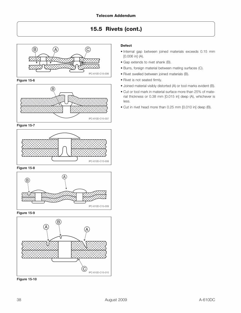
Defect
• Internal gap between joined materials exceeds 0.15 mm[0.006 in] (A).
• Gap extends to rivet shank (B).
• Burrs, foreign material between mating surfaces (C).
• Rivet swelled between joined materials (B).
• Rivet is not seated firmly.
• Joined material visibly distorted (A) or tool marks evident (B).
• Cut or tool mark in material surface more than 25% of mate-rial thickness or 0.38 mm [0.015 in] deep (A), whichever isless.
• Cut in rivet head more than 0.25 mm [0.010 in] deep (B).
AB C
IPC-610D-C15-006
Figure 15-6
B
IPC-610D-C15-007
Figure 15-7
IPC-610D-C15-008
Figure 15-8
AB
IPC-610D-C15-009
Figure 15-9
AA
C
B
IPC-610D-C15-010
Figure 15-10
Telecom Addendum
15.5 Rivets (cont.)
38 A-610DCAugust 2009
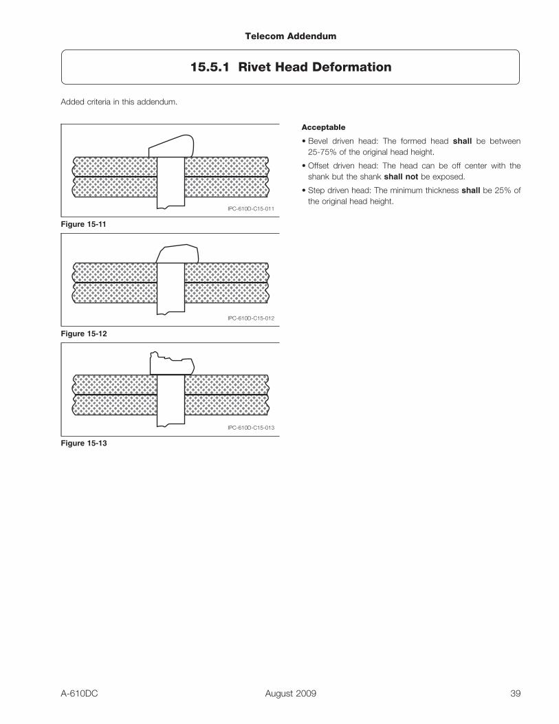
Added criteria in this addendum.
Acceptable
• Bevel driven head: The formed head shall be between25-75% of the original head height.
• Offset driven head: The head can be off center with theshank but the shank shall not be exposed.
• Step driven head: The minimum thickness shall be 25% ofthe original head height.
IPC-610D-C15-011
Figure 15-11
IPC-610D-C15-012
Figure 15-12
IPC-610D-C15-013
Figure 15-13
Telecom Addendum
15.5.1 Rivet Head Deformation
39A-610DC August 2009

Added criteria in this addendum.
Acceptable
• Rivet tight against mounting surface.
• Rollover complete.
• Edge of hole not visible.
• Gap equal to or less than 0.051 mm [0.002 in].
• Splits in the head of the rivet are acceptable providing thereare no more than 3, all spaced greater than 90° apart, andthey do not extend into the rivet shank.
• Pop rivets do not need to have a captive mandrel present aslong as the secondary head is fully formed.
Defect
• Rivet not tight against mounting surface.
• Rollover incomplete.
• Edge of hole visible.
• Gap greater than 0.051 mm [0.002 in].
• More than 3 splits in the head of the rivet or excessivebulges that may weaken the rivet.
• Secondary head on pop rivet is not fully formed and rivet isloose.
• Rivet too short and does not form proper rollover (A).
• Driven head flattened, formed with improper tool (B).
• Insufficient forming, bulged ends not curled (C).
IPC-610D-C15-014
Figure 15-14
A
C
B
IPC-610D-C15-015
Figure 15-15
A B CIPC-610D-C15-016
Figure 15-16
Telecom Addendum
15.5.2 Tubular and Pop Rivets
40 A-610DCAugust 2009
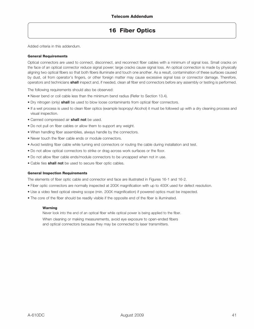
Added criteria in this addendum.
General Requirements
Optical connectors are used to connect, disconnect, and reconnect fiber cables with a minimum of signal loss. Small cracks onthe face of an optical connector reduce signal power; large cracks cause signal loss. An optical connection is made by physicallyaligning two optical fibers so that both fibers illuminate and touch one another. As a result, contamination of these surfaces causedby dust, oil from operator’s fingers, or other foreign matter may cause excessive signal loss or connector damage. Therefore,operators and technicians shall inspect and, if needed, clean all fiber end connectors before any assembly or testing is performed.
The following requirements should also be observed:
• Never bend or coil cable less than the minimum bend radius (Refer to Section 13.4).
• Dry nitrogen (only) shall be used to blow loose contaminants from optical fiber connectors.
• If a wet process is used to clean fiber optics (example Isopropyl Alcohol) it must be followed up with a dry cleaning process andvisual inspection.
• Canned compressed air shall not be used.
• Do not pull on fiber cables or allow them to support any weight.
• When handling fiber assemblies, always handle by the connectors.
• Never touch the fiber cable ends or module connectors.
• Avoid twisting fiber cable while turning end connectors or routing the cable during installation and test.
• Do not allow optical connectors to strike or drag across work surfaces or the floor.
• Do not allow fiber cable ends/module connectors to be uncapped when not in use.
• Cable ties shall not be used to secure fiber optic cables.
General Inspection Requirements
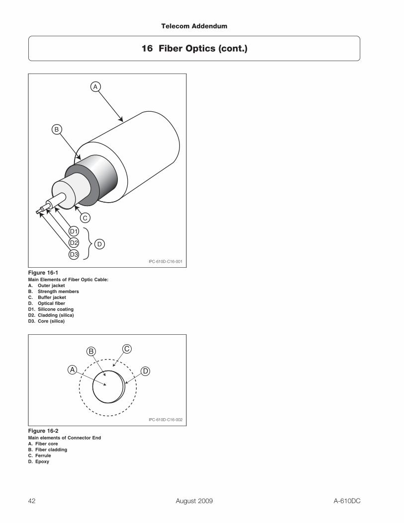
The elements of fiber optic cable and connector end face are illustrated in Figures 16-1 and 16-2.
• Fiber optic connectors are normally inspected at 200X magnification with up to 400X used for defect resolution.
• Use a video feed optical viewing scope (min. 200X magnification) if powered optics must be inspected.
• The core of the fiber should be readily visible if the opposite end of the fiber is illuminated.
WarningNever look into the end of an optical fiber while optical power is being applied to the fiber.
When cleaning or making measurements, avoid eye exposure to open-ended fibersand optical connectors because they may be connected to laser transmitters.
Telecom Addendum
16 Fiber Optics
41A-610DC August 2009
D1
C
D
B
A
D2
D3IPC-610D-C16-001
Figure 16-1Main Elements of Fiber Optic Cable:A. Outer jacketB. Strength membersC. Buffer jacketD. Optical fiberD1. Silicone coatingD2. Cladding (silica)D3. Core (silica)
A
B C
D
IPC-610D-C16-002
Figure 16-2Main elements of Connector EndA. Fiber coreB. Fiber claddingC. FerruleD. Epoxy
Telecom Addendum
16 Fiber Optics (cont.)
42 A-610DCAugust 2009
Added criteria in this addendum.
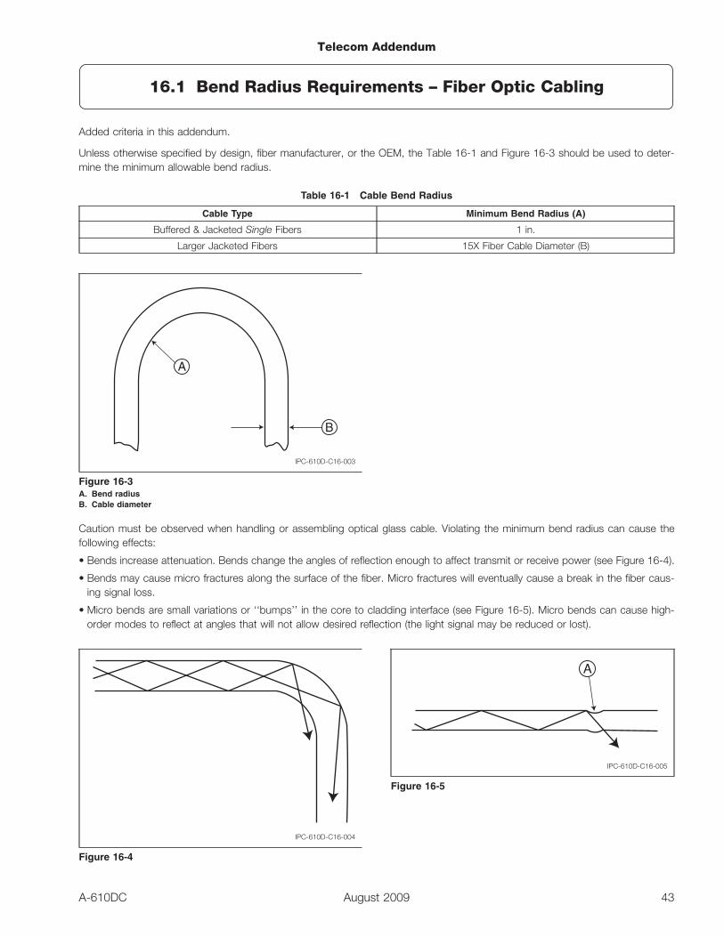
Unless otherwise specified by design, fiber manufacturer, or the OEM, the Table 16-1 and Figure 16-3 should be used to deter-mine the minimum allowable bend radius.
Table 16-1 Cable Bend Radius
Cable Type Minimum Bend Radius (A)
Buffered & Jacketed Single Fibers 1 in.
Larger Jacketed Fibers 15X Fiber Cable Diameter (B)
Caution must be observed when handling or assembling optical glass cable. Violating the minimum bend radius can cause thefollowing effects:
• Bends increase attenuation. Bends change the angles of reflection enough to affect transmit or receive power (see Figure 16-4).
• Bends may cause micro fractures along the surface of the fiber. Micro fractures will eventually cause a break in the fiber caus-ing signal loss.
• Micro bends are small variations or ‘‘bumps’’ in the core to cladding interface (see Figure 16-5). Micro bends can cause high-order modes to reflect at angles that will not allow desired reflection (the light signal may be reduced or lost).
A
B
IPC-610D-C16-003
Figure 16-3A. Bend radiusB. Cable diameter
IPC-610D-C16-004
Figure 16-4
A
IPC-610D-C16-005
Figure 16-5
Telecom Addendum
16.1 Bend Radius Requirements – Fiber Optic Cabling
43A-610DC August 2009
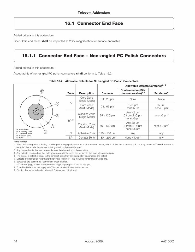
Added criteria in this addendum.
Fiber Optic end faces shall be inspected at 200x magnification for surface anomalies.
Added criteria in this addendum.
Acceptability of non-angled PC polish connectors shall conform to Table 16.2.
Table 16-2 Allowable Defects for Non-angled PC Polish Connectors
E
A
B
C
D
Zone Description Diameter
Allowable Defects/Scratches2, 3
Contamination/Pits(non-removable)4, 5 Scratches6
A
Core Zone(Single-Mode) 0 to 25 µm None None
Core Zone(Multi-Mode) 0 to 66 µm 5 <5 µm
none 5 µm5 µm
none 3 µm
B7, 9
Cladding Zone(Single-Mode) 25 - 120 µm
Any <2 µm5 from 2 -5 µm
none >5 µmnone >3 µm1
Cladding Zone(Multi-Mode) 66 - 130 µm
Any <2 µm8 from 2 -5 µm
none >5 µmnone >3 µm1
C Adhesive Zone 120 - 130 µm any any
D8 Contact Zone 130 - 250 µm None >10 µm anyTable Notes:1) When inspecting after polishing or while performing quality assurance of a new connector, a limit of five fine scratches (<3 µm) may be set in Zone B in order to
establish that a reliable process is being used by the manufacturer.2) Any contaminants that are removable must be cleaned from the end-face.3) Any defects or scratches that extend across multiple zones are subject to the most stringent criteria.4) The size of a defect is equal to the smallest circle that can completely encompass the defect.5) Defects are defined as ‘‘permanent nonlinear features.’’ This includes contamination, pits, etc.6) Scratches are defined as ‘‘permanent linear features.’’7) MT ferrules (e.g., ribbon) have allowable edge chipping from 115 to 125 µm.8) Zone D criteria does not apply to MT-ferrule or Metallic-ferrule connectors.9) Cracks, that when extended intersect Zone A, are not allowed.
A. Core ZoneB. Cladding ZoneC. Adhesive ZoneD. Contact ZoneE. Core
Telecom Addendum
16.1 Connector End Face
44 A-610DCAugust 2009
16.1.1 Connector End Face – Non-angled PC Polish Connectors
Added criteria in this addendum.
Acceptability of receptacles (with internal fiber stubs) shall conform to Table 16-3.
Table 16-3 Allowable Defects for Receptacles (with internal fiber stubs)
Zone Description Diameter
Allowable Defects/Scratches2, 3
Contamination/Pits(non-removable)
4, 5Scratches6
ACore Zone (Single-Mode) 0 to 25 µm None None
Core Zone (Multi-Mode) 0 to 66 µm 5 <5 µmnone >5 µm
5 <3 µmnone >3 µm
B7, 9
Cladding Zone (Single-Mode) 25 - 120 µmAny <5 µm
5 from 5 -10 µmnone >10 µm
none >3 µm1
Cladding Zone (Multi-Mode) 66 -130 µmAny <5 µm
8 from 5 -10 µmnone >10 µm
none >3 µm1
C Adhesive Zone 120 - 130 µm any any
D7, 8 Contact Zone 130 - 250 µmany <20 µm
3 from 20 - 50 µmNone >50 µm
any
Notes:1) When inspecting after polishing or while performing quality assurance of a new connector, a limit of five fine scratches (<3 µm) may be set in Zone B in order to
establish that a reliable process is being used by the manufacturer.2) Any contaminants that are removable must be cleaned from the end-face.3) Any defects or scratches that extend across multiple zones are subject to the most stringent criteria.4) The size of a defect is equal to the smallest circle that can completely encompass the defect.5) Defects are defined as ‘‘permanent nonlinear features.’’ This includes contamination, pits, etc.6) Scratches are defined as ‘‘permanent linear features.’’7) MT ferrules (e.g., ribbon) have allowable edge chipping from 115 to 125 µm.8) Zone D criteria does not apply to MT-ferrule or Metallic-ferrule connectors.9) Cracks, that when extended intersect Zone A, are not allowed.
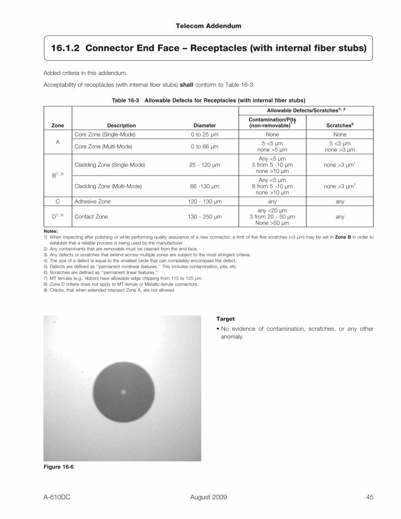
Target
• No evidence of contamination, scratches, or any otheranomaly.
Figure 16-6
Telecom Addendum
16.1.2 Connector End Face – Receptacles (with internal fiber stubs)
45A-610DC August 2009
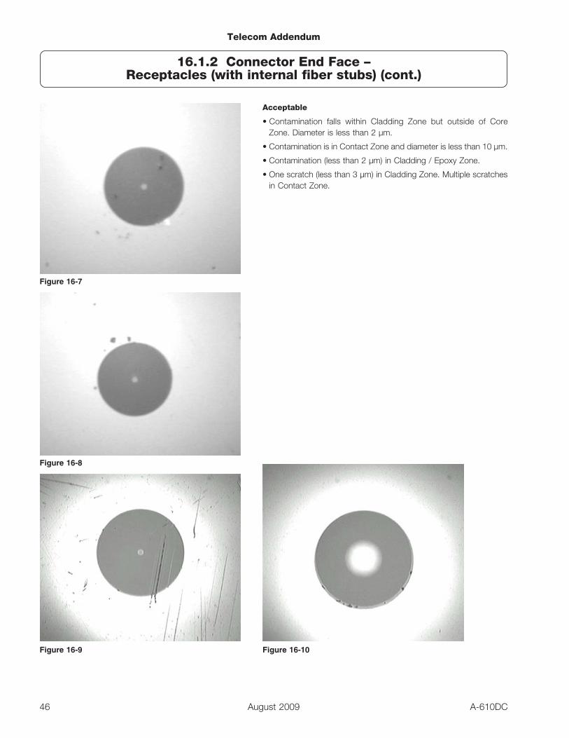
Acceptable
• Contamination falls within Cladding Zone but outside of CoreZone. Diameter is less than 2 µm.
• Contamination is in Contact Zone and diameter is less than 10 µm.
• Contamination (less than 2 µm) in Cladding / Epoxy Zone.
• One scratch (less than 3 µm) in Cladding Zone. Multiple scratchesin Contact Zone.
Figure 16-7
Figure 16-8
Figure 16-9 Figure 16-10
Telecom Addendum
16.1.2 Connector End Face –Receptacles (with internal fiber stubs) (cont.)
46 A-610DCAugust 2009
Defect
• Heavy cracks and chips.
• Core area damaged.
Defect
• Fiber surface pulverized by rotational contact with mating connector.(‘‘Crashed’’)
Defect
• Severe chipping and cracking. (‘‘Crashed’’)
Figure 16-11
Figure 16-12
Figure 16-13
Telecom Addendum
16.1.2 Connector End Face –Receptacles (with internal fiber stubs) (cont.)
47A-610DC August 2009
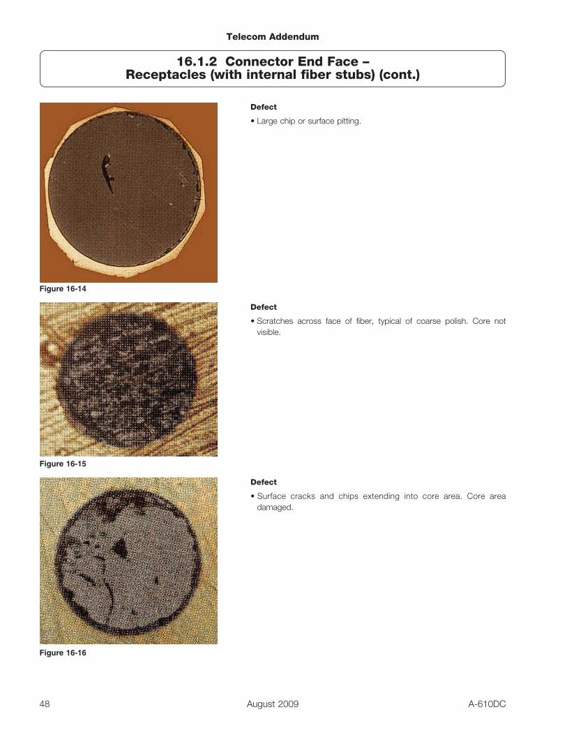
Defect
• Large chip or surface pitting.
Defect
• Scratches across face of fiber, typical of coarse polish. Core notvisible.
Defect
• Surface cracks and chips extending into core area. Core areadamaged.
Figure 16-14
Figure 16-15
Figure 16-16
Telecom Addendum
16.1.2 Connector End Face –Receptacles (with internal fiber stubs) (cont.)
48 A-610DCAugust 2009
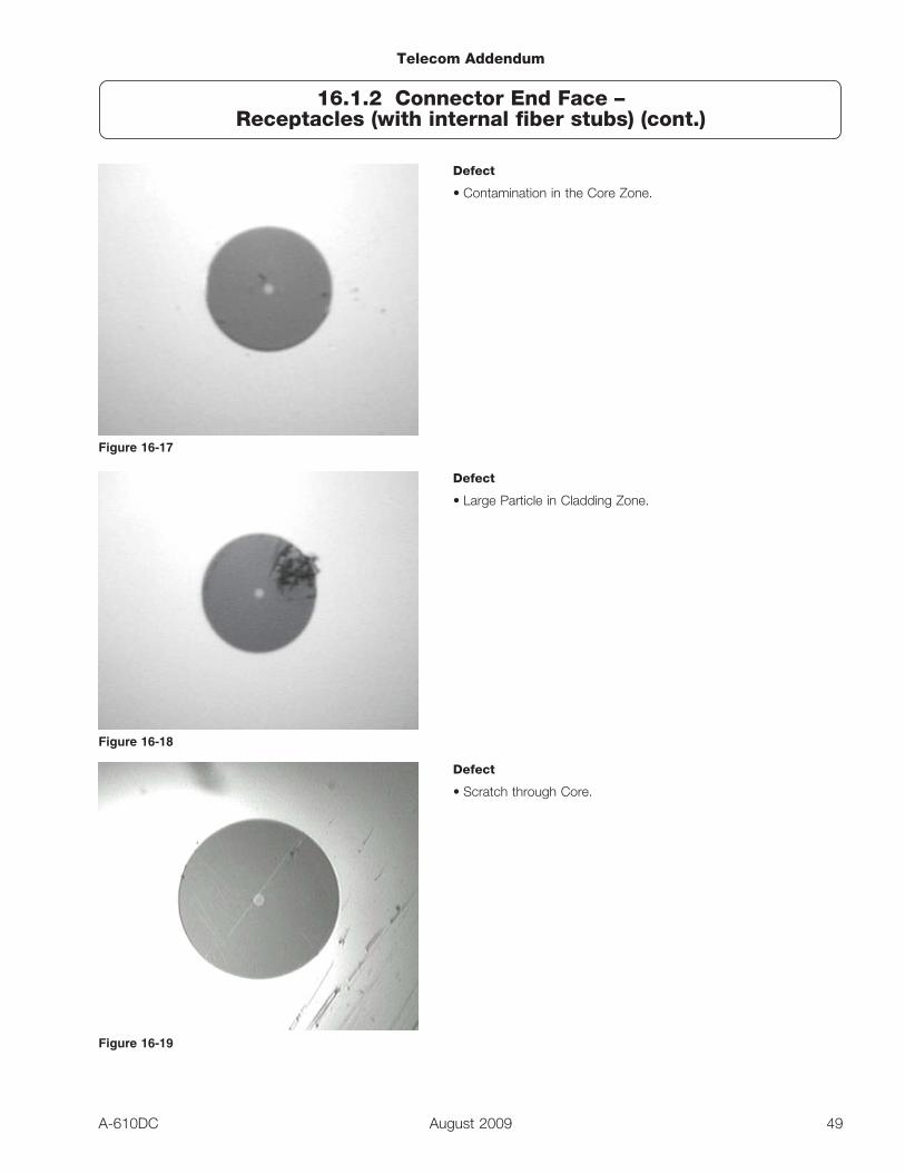
Defect
• Contamination in the Core Zone.
Defect
• Large Particle in Cladding Zone.
Defect
• Scratch through Core.
Figure 16-17
Figure 16-18
Figure 16-19
Telecom Addendum
16.1.2 Connector End Face –Receptacles (with internal fiber stubs) (cont.)
49A-610DC August 2009
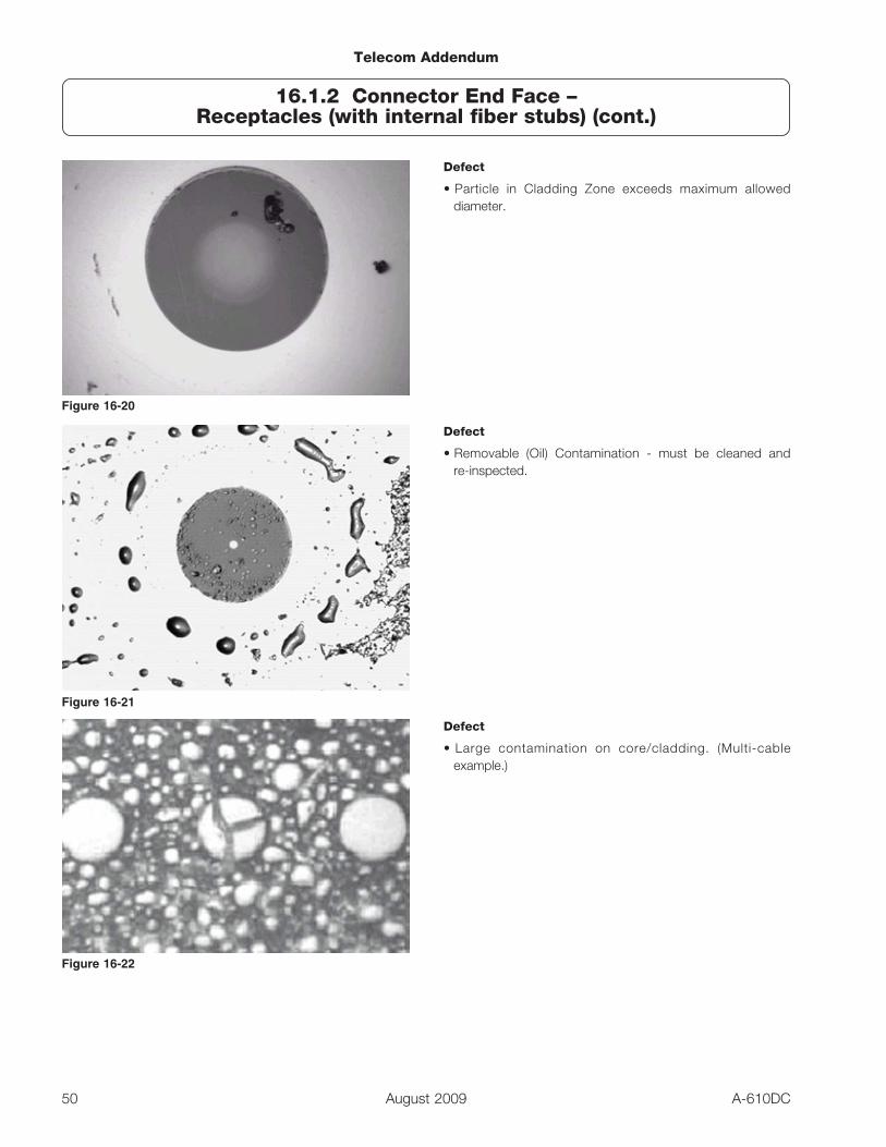
Defect
• Particle in Cladding Zone exceeds maximum alloweddiameter.
Defect
• Removable (Oil) Contamination - must be cleaned andre-inspected.
Defect
• Large contamination on core/cladding. (Multi-cableexample.)
Figure 16-20
Figure 16-21
Figure 16-22
Telecom Addendum
16.1.2 Connector End Face –Receptacles (with internal fiber stubs) (cont.)
50 A-610DCAugust 2009
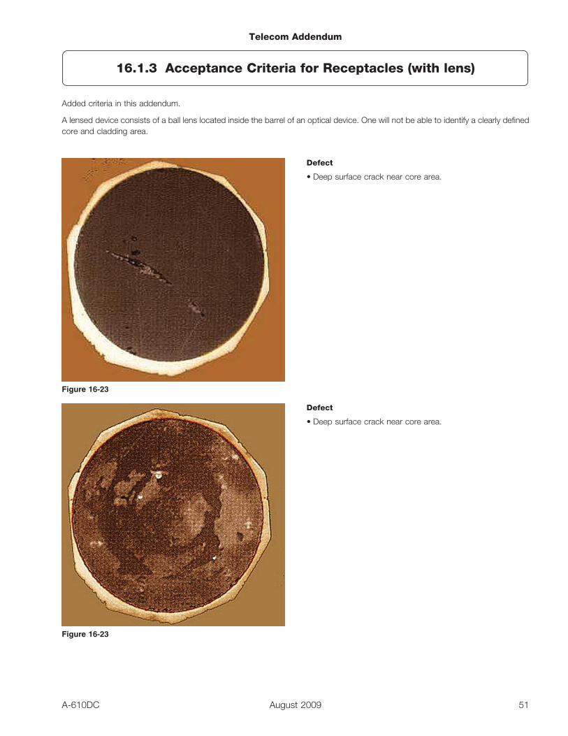
Added criteria in this addendum.
A lensed device consists of a ball lens located inside the barrel of an optical device. One will not be able to identify a clearly definedcore and cladding area.
Defect
• Deep surface crack near core area.
Defect
• Deep surface crack near core area.
Figure 16-23
Figure 16-23
Telecom Addendum
16.1.3 Acceptance Criteria for Receptacles (with lens)
51A-610DC August 2009
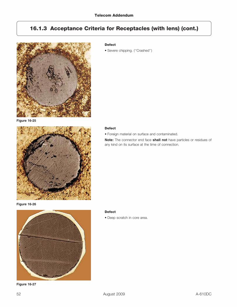
Defect
• Severe chipping. (‘‘Crashed’’)
Defect
• Foreign material on surface and contaminated.
Note: The connector end face shall not have particles or residues ofany kind on its surface at the time of connection.
Defect
• Deep scratch in core area.
Figure 16-25
Figure 16-26
Figure 16-27
Telecom Addendum
16.1.3 Acceptance Criteria for Receptacles (with lens) (cont.)
52 A-610DCAugust 2009
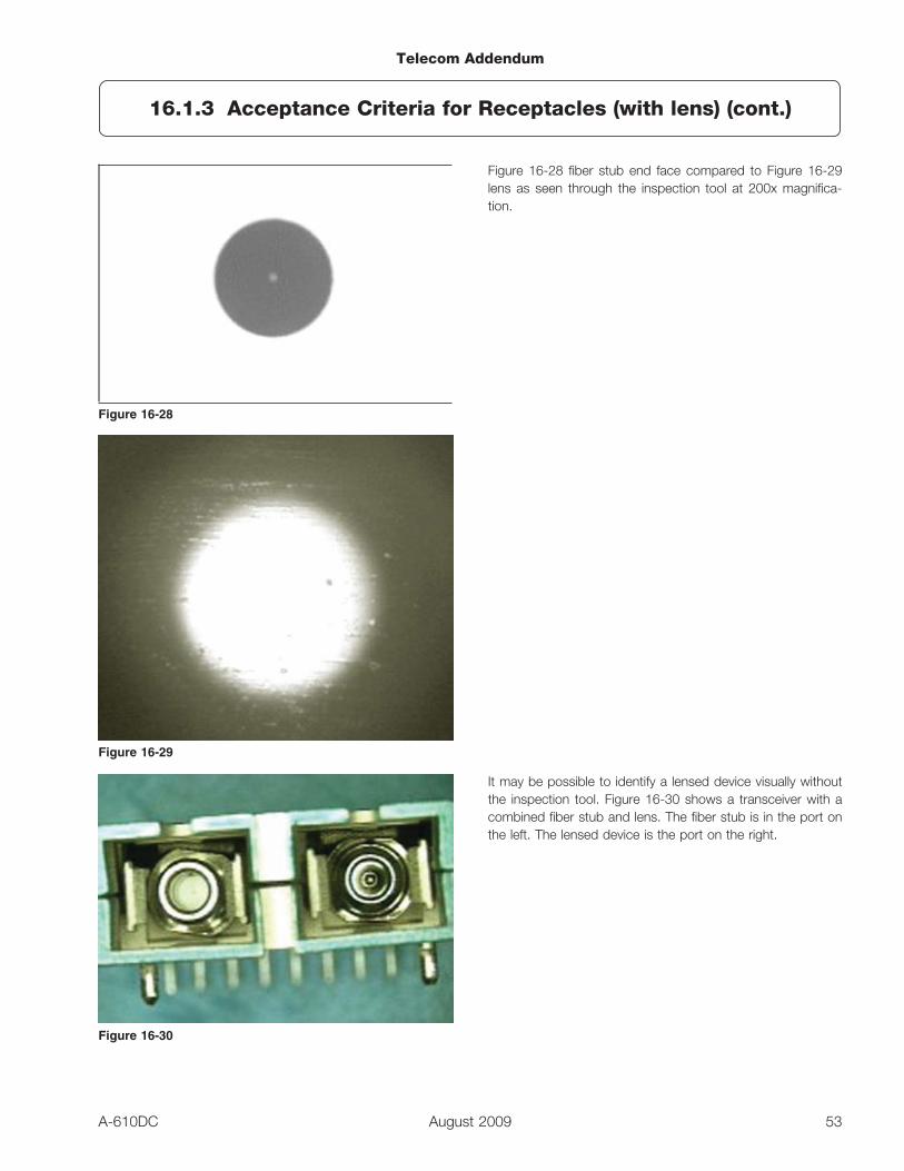
Figure 16-28 fiber stub end face compared to Figure 16-29lens as seen through the inspection tool at 200x magnifica-tion.
It may be possible to identify a lensed device visually withoutthe inspection tool. Figure 16-30 shows a transceiver with acombined fiber stub and lens. The fiber stub is in the port onthe left. The lensed device is the port on the right.
Figure 16-28
Figure 16-29
Figure 16-30
Telecom Addendum
16.1.3 Acceptance Criteria for Receptacles (with lens) (cont.)
53A-610DC August 2009
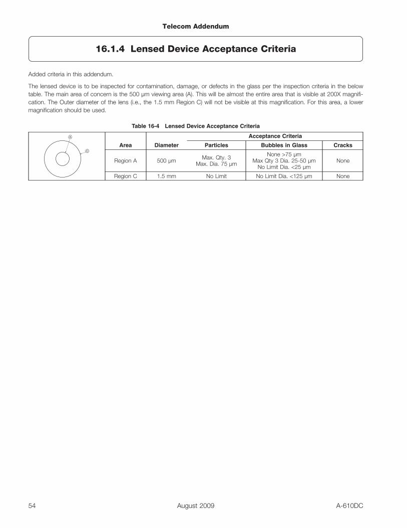
Added criteria in this addendum.
The lensed device is to be inspected for contamination, damage, or defects in the glass per the inspection criteria in the belowtable. The main area of concern is the 500 µm viewing area (A). This will be almost the entire area that is visible at 200X magnifi-cation. The Outer diameter of the lens (i.e., the 1.5 mm Region C) will not be visible at this magnification. For this area, a lowermagnification should be used.
Table 16-4 Lensed Device Acceptance Criteria
A
C
Area Diameter
Acceptance Criteria
Particles Bubbles in Glass Cracks
Region A 500 µm Max. Qty. 3Max. Dia. 75 µm
None >75 µmMax Qty 3 Dia. 25-50 µm
No Limit Dia. <25 µmNone
Region C 1.5 mm No Limit No Limit Dia. <125 µm None
Telecom Addendum
16.1.4 Lensed Device Acceptance Criteria
54 A-610DCAugust 2009
Added criteria in this addendum.
Target
• No damage to jacket.
Acceptable
• Slight discoloration/melting are acceptable if caused by inci-dental contact with soldering iron during assembly orrework.
• Damage shall not expose fiber.
Defect
• Melted jacket with visibly burned (charred) area.
• Discoloration/melting related to power/heat sources con-tained within the effected assembly.
• Any cut or burn that exposes inner layers.
• Jacket with compression marks evident.
• Possible crushed fiberglass core.
Figure 16-31
Figure 16-32
Figure 16-33
Figure 16-34
Telecom Addendum
16.1.5 Fiber Optic Cable Insulation Damage
55A-610DC August 2009
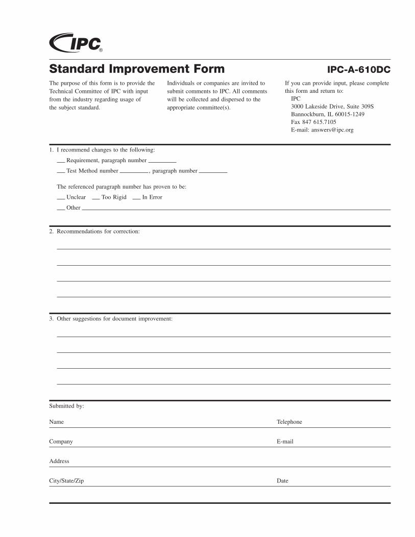
Standard Improvement Form IPC-A-610DCThe purpose of this form is to provide theTechnical Committee of IPC with inputfrom the industry regarding usage ofthe subject standard.
Individuals or companies are invited tosubmit comments to IPC. All commentswill be collected and dispersed to theappropriate committee(s).
If you can provide input, please completethis form and return to:
IPC3000 Lakeside Drive, Suite 309SBannockburn, IL 60015-1249Fax 847 615.7105E-mail: [email protected]
1. I recommend changes to the following:
Requirement, paragraph number
Test Method number , paragraph number
The referenced paragraph number has proven to be:
Unclear Too Rigid In Error
Other
2. Recommendations for correction:
3. Other suggestions for document improvement:
Submitted by:
Name Telephone
Company E-mail
Address
City/State/Zip Date
®
847-615-7100 tel 847-615-7105 fax www.ipc.org
3000 Lakeside Drive, Suite 309 SBannockburn, IL 60015
Association Connecting Electronics Industries
®