Embed Size (px)
Citation preview
www.irf.com 1
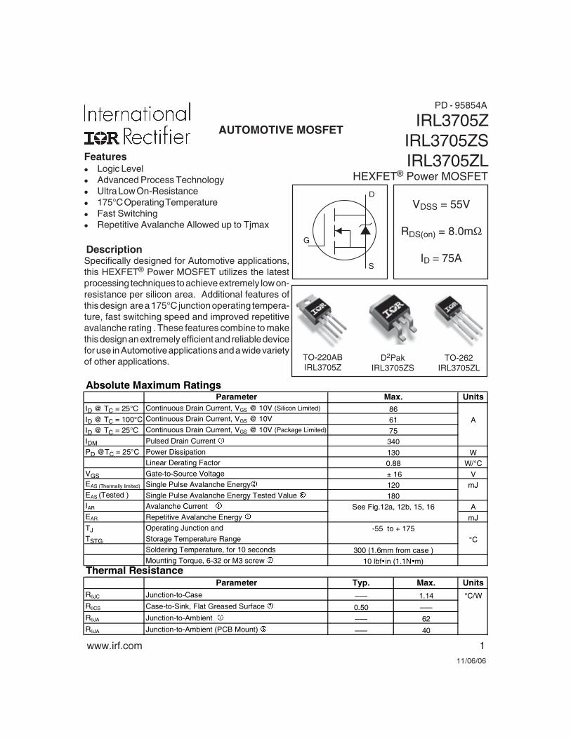
AUTOMOTIVE MOSFET
HEXFET® Power MOSFET
VDSS = 55V
RDS(on) = 8.0mΩ
ID = 75ASpecifically designed for Automotive applications,this HEXFET® Power MOSFET utilizes the latestprocessing techniques to achieve extremely low on-resistance per silicon area. Additional features ofthis design are a 175°C junction operating tempera-ture, fast switching speed and improved repetitiveavalanche rating . These features combine to makethis design an extremely efficient and reliable devicefor use in Automotive applications and a wide varietyof other applications.
S
D
GDescription
Features Logic Level Advanced Process Technology Ultra Low On-Resistance 175°C Operating Temperature Fast Switching Repetitive Avalanche Allowed up to Tjmax
IRL3705ZIRL3705ZSIRL3705ZL
D2PakIRL3705ZS
TO-220ABIRL3705Z
TO-262IRL3705ZL
Absolute Maximum RatingsParameter Units
ID @ TC = 25°C Continuous Drain Current, VGS @ 10V (Silicon Limited)
ID @ TC = 100°C Continuous Drain Current, VGS @ 10V AID @ TC = 25°C Continuous Drain Current, VGS @ 10V (Package Limited)
IDM Pulsed Drain Current
PD @TC = 25°C Power Dissipation WLinear Derating Factor W/°C
VGS Gate-to-Source Voltage VEAS (Thermally limited) Single Pulse Avalanche Energy mJEAS (Tested ) Single Pulse Avalanche Energy Tested Value IAR Avalanche Current AEAR Repetitive Avalanche Energy mJTJ Operating Junction and
TSTG Storage Temperature Range °CSoldering Temperature, for 10 seconds
Mounting Torque, 6-32 or M3 screw
Thermal ResistanceParameter Typ. Max. Units
RθJC Junction-to-Case ––– 1.14 °C/WRθCS Case-to-Sink, Flat Greased Surface 0.50 –––RθJA Junction-to-Ambient ––– 62RθJA Junction-to-Ambient (PCB Mount) ––– 40
-55 to + 175
300 (1.6mm from case )
10 lbfin (1.1Nm)
1300.88
± 16
Max.8661
34075
180
120
See Fig.12a, 12b, 15, 16
PD - 95854A
2 www.irf.com
S
D
G
S
D
G
Electrical Characteristics @ TJ = 25°C (unless otherwise specified)Parameter Min. Typ. Max. Units
V(BR)DSS Drain-to-Source Breakdown Voltage 55 ––– ––– V
∆V(BR)DSS/∆TJ Breakdown Voltage Temp. Coefficient ––– 0.055 ––– V/°C
––– 6.5 8.0
RDS(on) Static Drain-to-Source On-Resistance ––– ––– 11 mΩ
––– ––– 12
VGS(th) Gate Threshold Voltage 1.0 ––– 3.0 V
gfs Forward Transconductance 150 ––– ––– V
IDSS Drain-to-Source Leakage Current ––– ––– 20 µA
––– ––– 250
IGSS Gate-to-Source Forward Leakage ––– ––– 200 nA
Gate-to-Source Reverse Leakage ––– ––– -200
Qg Total Gate Charge ––– 40 60
Qgs Gate-to-Source Charge ––– 12 ––– nC
Qgd Gate-to-Drain ("Miller") Charge ––– 21 –––
td(on) Turn-On Delay Time ––– 17 –––
tr Rise Time ––– 240 ––– ns
td(off) Turn-Off Delay Time ––– 26 –––
tf Fall Time ––– 83 –––
LD Internal Drain Inductance ––– 4.5 ––– Between lead,
nH 6mm (0.25in.)LS Internal Source Inductance ––– 7.5 ––– from package
and center of die contactCiss Input Capacitance ––– 2880 –––
Coss Output Capacitance ––– 420 –––
Crss Reverse Transfer Capacitance ––– 220 ––– pFCoss Output Capacitance ––– 1500 –––
Coss Output Capacitance ––– 330 –––
Coss eff. Effective Output Capacitance ––– 510 –––
Source-Drain Ratings and Characteristics Parameter Min. Typ. Max. Units
IS Continuous Source Current ––– ––– 75
(Body Diode) AISM Pulsed Source Current ––– ––– 340
(Body Diode)VSD Diode Forward Voltage ––– ––– 1.3 Vtrr Reverse Recovery Time ––– 16 24 nsQrr Reverse Recovery Charge ––– 7.4 11 nCton Forward Turn-On Time Intrinsic turn-on time is negligible (turn-on is dominated by LS+LD)
VGS = 5.0V
VDD = 28V
ID = 43A
RG = 4.3 Ω
TJ = 25°C, IS = 52A, VGS = 0V
TJ = 25°C, IF = 43A, VDD = 28Vdi/dt = 100A/µs
ConditionsVGS = 0V, ID = 250µAReference to 25°C, ID = 1mA
VGS = 10V, ID = 52A
VDS = VGS, ID = 250µA
VDS = 55V, VGS = 0V
VDS = 55V, VGS = 0V, TJ = 125°C
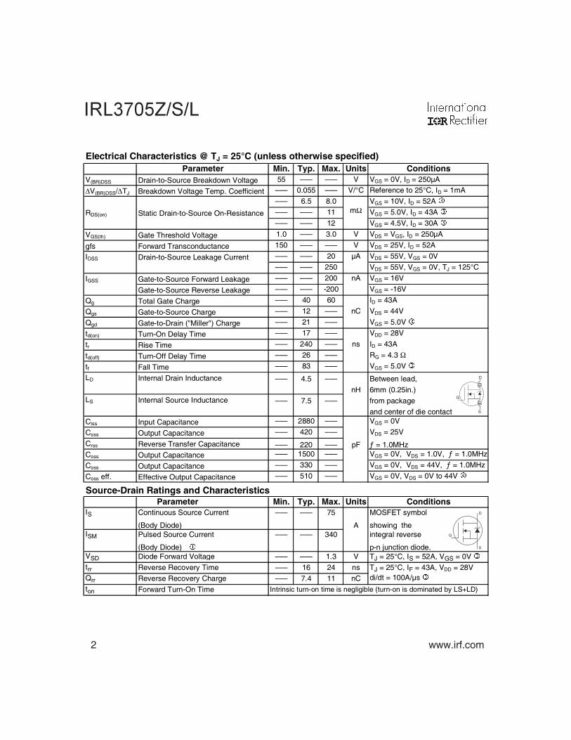
MOSFET symbol
showing theintegral reverse
p-n junction diode.
Conditions
VGS = 5.0V
VGS = 0V
VDS = 25V
ƒ = 1.0MHzVGS = 0V, VDS = 1.0V, ƒ = 1.0MHz
VGS = 0V, VDS = 44V, ƒ = 1.0MHz
VGS = 0V, VDS = 0V to 44V
VGS = 5.0V, ID = 43A
VDS = 25V, ID = 52A
ID = 43A
VDS = 44V
VGS = 16V
VGS = -16V
VGS = 4.5V, ID = 30A
www.irf.com 3
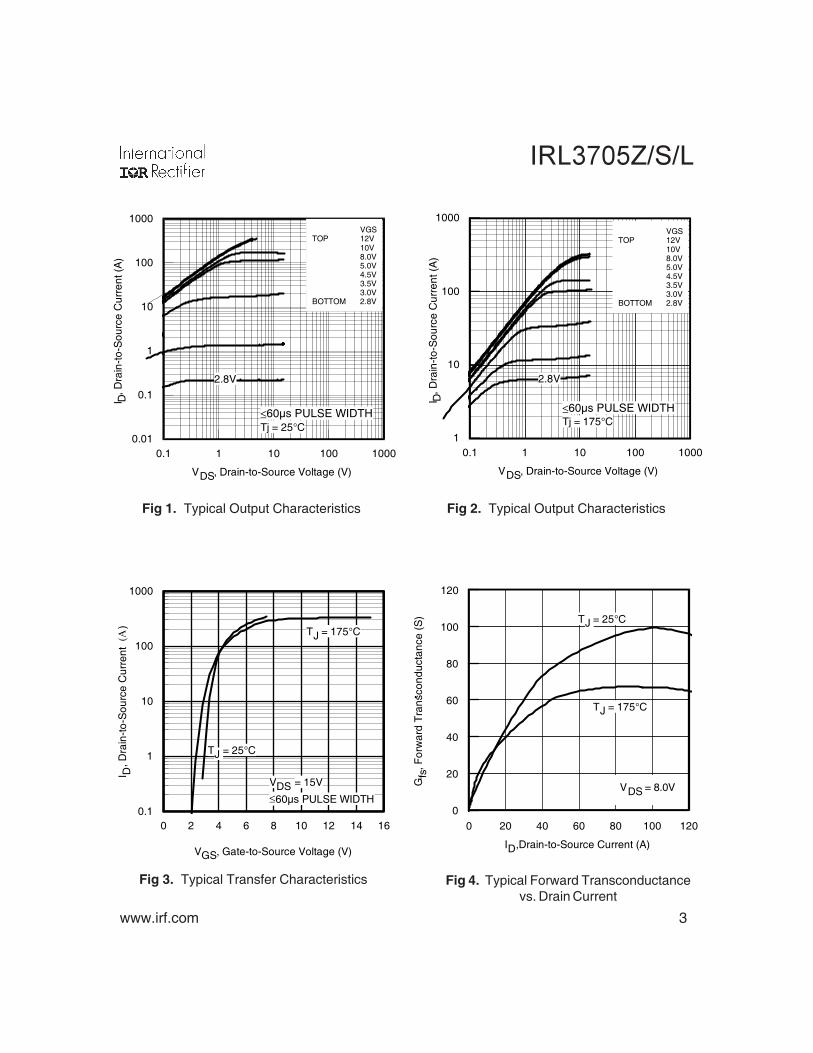
Fig 2. Typical Output CharacteristicsFig 1. Typical Output Characteristics
Fig 3. Typical Transfer Characteristics Fig 4. Typical Forward Transconductancevs. Drain Current
0.1 1 10 100 1000
VDS, Drain-to-Source Voltage (V)
0.01
0.1
1
10
100
1000
I D, D
rain
-to-
Sou
rce
Cur
rent
(A
)
VGSTOP 12V
10V8.0V5.0V4.5V3.5V3.0V
BOTTOM 2.8V
≤60µs PULSE WIDTHTj = 25°C
2.8V
0.1 1 10 100 1000
VDS, Drain-to-Source Voltage (V)
1
10
100
1000
I D, D
rain
-to-
Sou
rce
Cur
rent
(A
)
2.8V
≤60µs PULSE WIDTHTj = 175°C
VGSTOP 12V
10V8.0V5.0V4.5V3.5V3.0V
BOTTOM 2.8V
0 2 4 6 8 10 12 14 16
VGS, Gate-to-Source Voltage (V)
0.1
1
10
100
1000
I D, D
rain
-to-
Sou
rce
Cur
rent
(Α
)
TJ = 25°C
TJ = 175°C
VDS = 15V
≤60µs PULSE WIDTH
0 20 40 60 80 100 120
ID,Drain-to-Source Current (A)
0
20
40
60
80
100
120
Gfs
, For
war
d T
rans
cond
ucta
nce
(S) TJ = 25°C
TJ = 175°C
VDS = 8.0V
4 www.irf.com
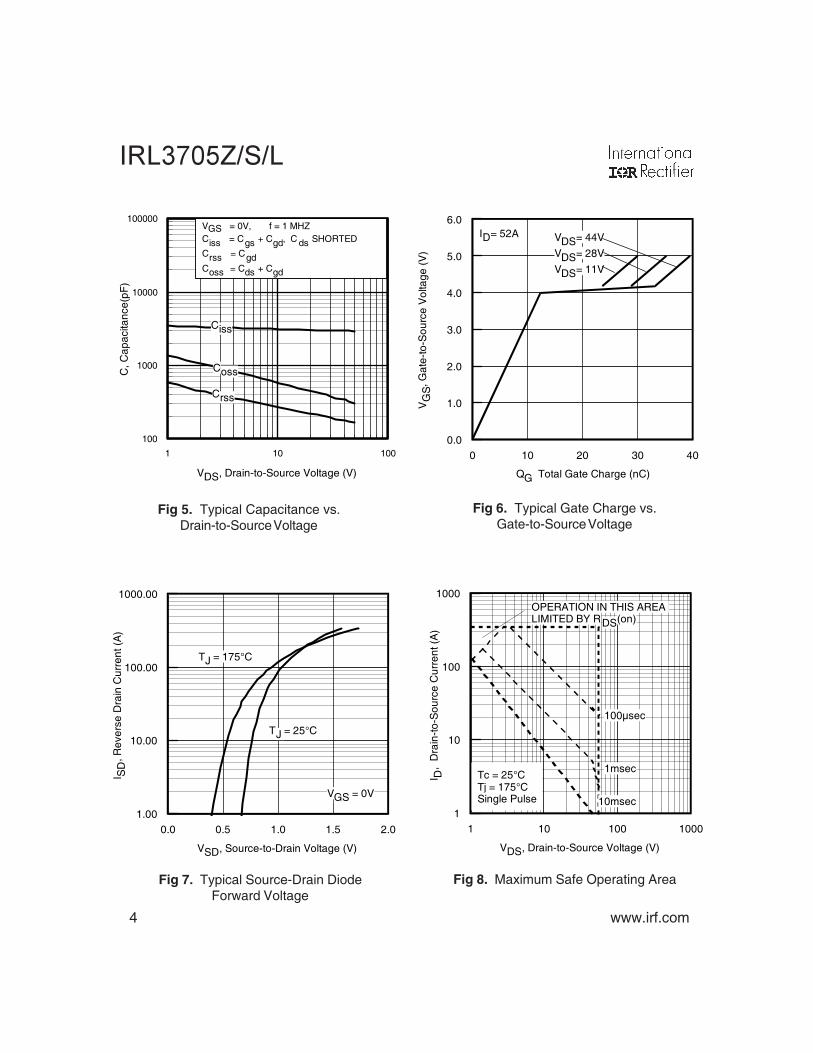
Fig 8. Maximum Safe Operating Area
Fig 6. Typical Gate Charge vs.Gate-to-Source Voltage
Fig 5. Typical Capacitance vs.Drain-to-Source Voltage
Fig 7. Typical Source-Drain DiodeForward Voltage
1 10 100
VDS, Drain-to-Source Voltage (V)
100
1000
10000
100000
C, C
apac
itanc
e(pF
)
VGS = 0V, f = 1 MHZCiss = Cgs + Cgd, C ds SHORTED
Crss = Cgd Coss = Cds + Cgd
Coss
Crss
Ciss
0 10 20 30 40
QG Total Gate Charge (nC)
0.0
1.0
2.0
3.0
4.0
5.0
6.0
VG
S, G
ate-
to-S
ourc
e V
olta
ge (
V)
VDS= 44V
VDS= 28V
VDS= 11V
ID= 52A
1 10 100 1000
VDS, Drain-to-Source Voltage (V)
1
10
100
1000
I D,
Dra
in-t
o-S
ourc
e C
urre
nt (
A)
1msec
10msec
OPERATION IN THIS AREA LIMITED BY RDS(on)
100µsec
Tc = 25°CTj = 175°CSingle Pulse
0.0 0.5 1.0 1.5 2.0
VSD, Source-to-Drain Voltage (V)
1.00
10.00
100.00
1000.00
I SD
, Rev
erse
Dra
in C
urre
nt (
A)
TJ = 25°C
TJ = 175°C
VGS = 0V
www.irf.com 5
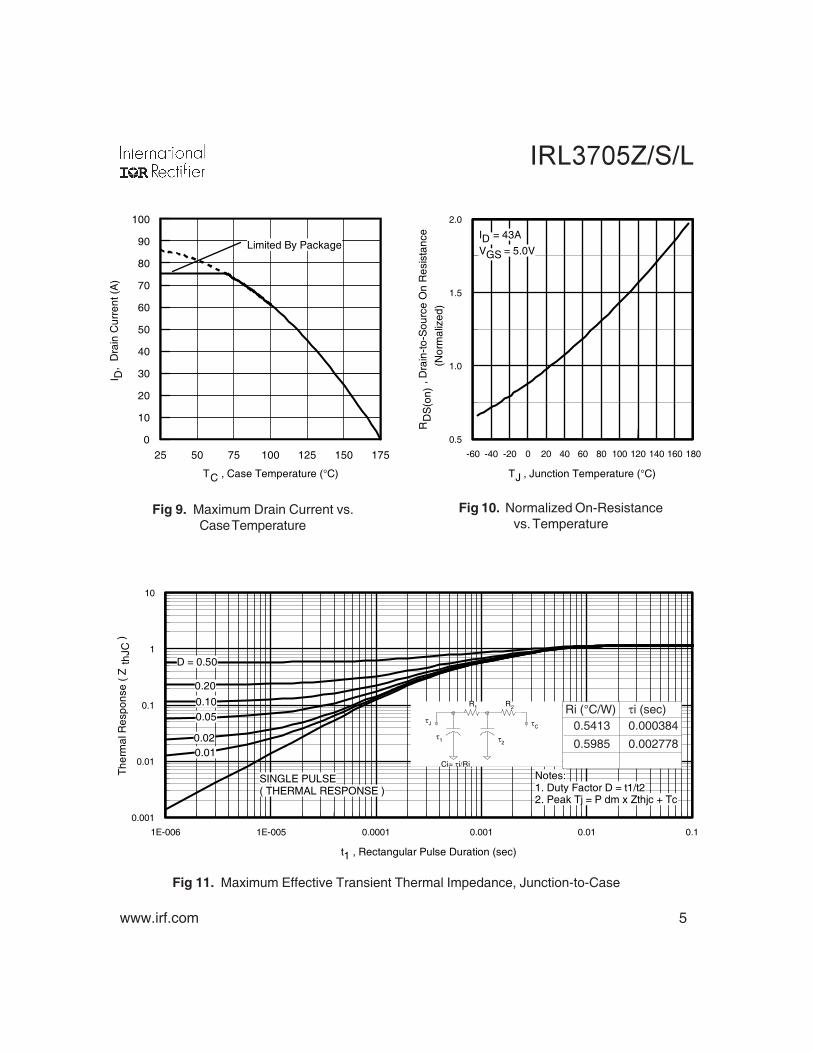
Fig 11. Maximum Effective Transient Thermal Impedance, Junction-to-Case
Fig 9. Maximum Drain Current vs.Case Temperature
Fig 10. Normalized On-Resistancevs. Temperature
-60 -40 -20 0 20 40 60 80 100 120 140 160 180
TJ , Junction Temperature (°C)
0.5
1.0
1.5
2.0
RD
S(o
n) ,
Dra
in-t
o-S
ourc
e O
n R
esis
tanc
e
(
Nor
mal
ized
)
ID = 43A
VGS = 5.0V
1E-006 1E-005 0.0001 0.001 0.01 0.1
t1 , Rectangular Pulse Duration (sec)
0.001
0.01
0.1
1
10
The
rmal
Res
pons
e (
Z th
JC )
0.20
0.10
D = 0.50
0.020.01
0.05
SINGLE PULSE( THERMAL RESPONSE )
Notes:1. Duty Factor D = t1/t22. Peak Tj = P dm x Zthjc + Tc
Ri (°C/W) τi (sec)0.5413 0.000384
0.5985 0.002778
τJ
τJ
τ1
τ1τ2
τ2
R1
R1 R2
R2
ττC
Ci i/RiCi= τi/Ri
25 50 75 100 125 150 175
TC , Case Temperature (°C)
0
10
20
30
40
50
60
70
80
90
100
I D,
Dra
in C
urre
nt (
A)
Limited By Package
6 www.irf.com
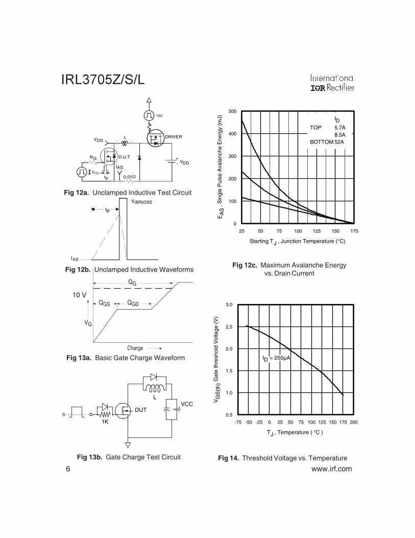
QG
QGS QGD
VG
Charge
Fig 13a. Basic Gate Charge Waveform
Fig 12c. Maximum Avalanche Energyvs. Drain CurrentFig 12b. Unclamped Inductive Waveforms
Fig 12a. Unclamped Inductive Test Circuit
tp
V(BR)DSS
IAS
Fig 14. Threshold Voltage vs. Temperature
RG
IAS
0.01Ωtp
D.U.T
LVDS
+- VDD
DRIVER
A
15V
20VVGS
1K
VCCDUT
0
L
Fig 13b. Gate Charge Test Circuit
25 50 75 100 125 150 175
Starting TJ , Junction Temperature (°C)
0
100
200
300
400
500
EA
S ,
Sin
gle
Pul
se A
vala
nche
Ene
rgy
(mJ) ID
TOP 5.7A8.5A
BOTTOM 52A
-75 -50 -25 0 25 50 75 100 125 150 175 200
TJ , Temperature ( °C )
0.5
1.0
1.5
2.0
2.5
3.0
VG
S(t
h) G
ate
thre
shol
d V
olta
ge (
V)
ID = 250µA
www.irf.com 7
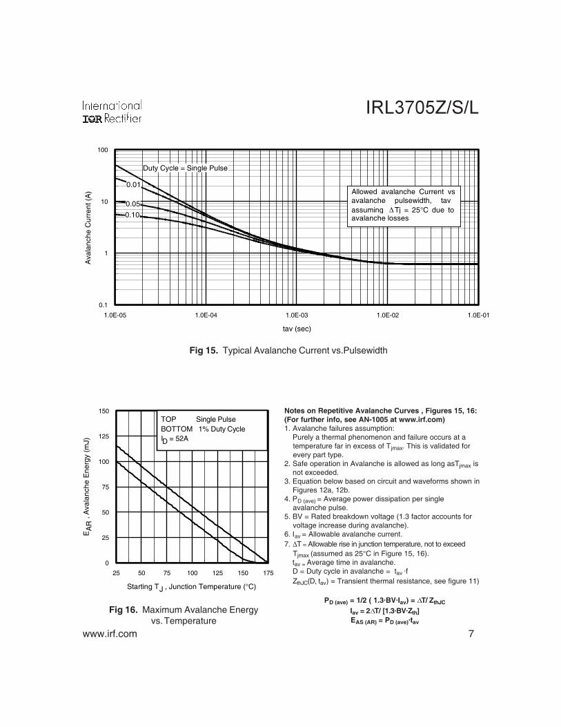
Fig 15. Typical Avalanche Current vs.Pulsewidth
Fig 16. Maximum Avalanche Energyvs. Temperature
Notes on Repetitive Avalanche Curves , Figures 15, 16:(For further info, see AN-1005 at www.irf.com)1. Avalanche failures assumption: Purely a thermal phenomenon and failure occurs at a
temperature far in excess of Tjmax. This is validated for every part type.2. Safe operation in Avalanche is allowed as long asTjmax is not exceeded.
3. Equation below based on circuit and waveforms shown in Figures 12a, 12b.
4. PD (ave) = Average power dissipation per single avalanche pulse.5. BV = Rated breakdown voltage (1.3 factor accounts for voltage increase during avalanche).6. Iav = Allowable avalanche current.7. ∆T = Allowable rise in junction temperature, not to exceed Tjmax (assumed as 25°C in Figure 15, 16). tav = Average time in avalanche. D = Duty cycle in avalanche = tav ·f ZthJC(D, tav) = Transient thermal resistance, see figure 11)
PD (ave) = 1/2 ( 1.3·BV·Iav) =T/ ZthJC
Iav = 2T/ [1.3·BV·Zth]EAS (AR) = PD (ave)·tav
1.0E-05 1.0E-04 1.0E-03 1.0E-02 1.0E-01
tav (sec)
0.1
1
10
100
Ava
lanc
he C
urre
nt (
A)
0.05
Duty Cycle = Single Pulse
0.10
Allowed avalanche Current vs avalanche pulsewidth, tav assuming ∆ Tj = 25°C due to avalanche losses
0.01
25 50 75 100 125 150 175
Starting TJ , Junction Temperature (°C)
0
25
50
75
100
125
150
EA
R ,
Ava
lanc
he E
nerg
y (m
J)
TOP Single Pulse BOTTOM 1% Duty CycleID = 52A
8 www.irf.com
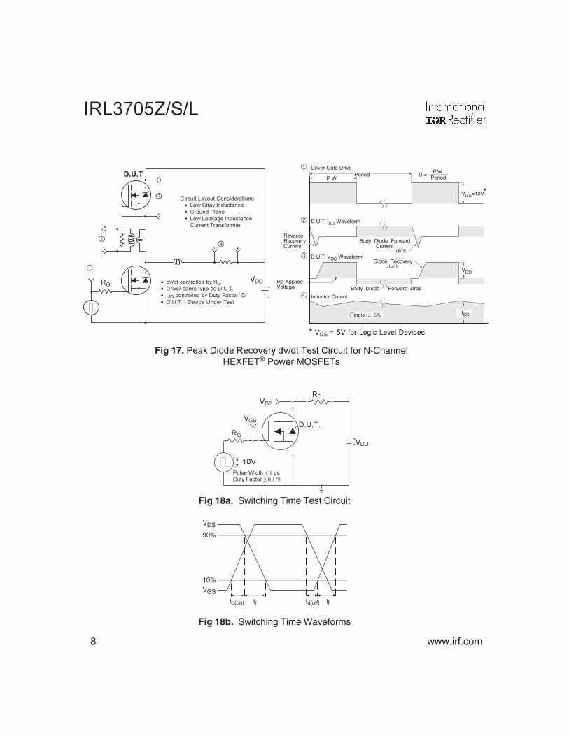
Fig 17. for N-ChannelHEXFETPower MOSFETs
• • •
P.W.Period
di/dt
Diode Recoverydv/dt
Ripple ≤ 5%
Body Diode Forward DropRe-AppliedVoltage
ReverseRecoveryCurrent
Body Diode ForwardCurrent
VGS=10V
VDD
ISD
Driver Gate Drive
D.U.T. ISD Waveform
D.U.T. VDS Waveform
Inductor Curent
D = P.W.Period
+
-
+
+
+-
-
-
•
• !"!!• #$$• !"!!%"
VDS
90%
10%VGS
td(on) tr td(off) tf
&'≤ 1 ( #≤ 0.1 %
+-
Fig 18a. Switching Time Test Circuit
Fig 18b. Switching Time Waveforms
www.irf.com 9
!""#$%&&!'()*)#$!+&# #$#$,#-% !&"!%,./!!"
" "
0
10 www.irf.com
!
www.irf.com 11
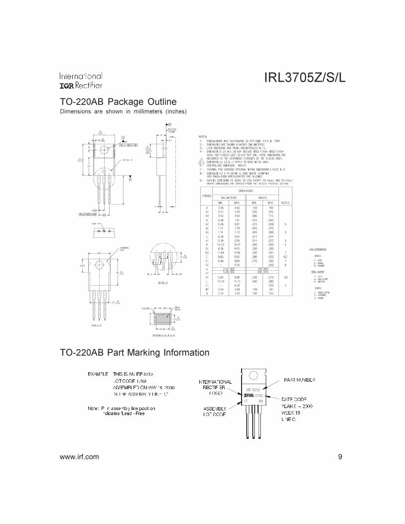
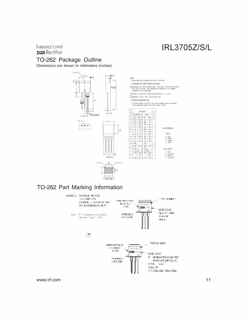
TO-262 Part Marking Information
TO-262 Package OutlineDimensions are shown in millimeters (inches)
!
"
##
12 www.irf.com
Data and specifications subject to change without notice. This product has been designed and qualified for the Automotive [Q101]market.
Qualification Standards can be found on IR’s Web site.
IR WORLD HEADQUARTERS: 233 Kansas St., El Segundo, California 90245, USA Tel: (310) 252-7105TAC Fax: (310) 252-7903
Visit us at www.irf.com for sales contact information. 11/06
TO-220AB package is not recommended for Surface Mount Application.
Repetitive rating; pulse width limited by max. junction temperature. (See fig. 11). Limited by TJmax, starting TJ = 25°C, L = 0.09mH RG = 25Ω, IAS = 52A, VGS =10V. Part not recommended for use above this value. Pulse width ≤ 1.0ms; duty cycle ≤ 2%. Coss eff. is a fixed capacitance that gives the same charging time as Coss while VDS is rising from 0 to 80% VDSS .
Limited by TJmax , see Fig.12a, 12b, 15, 16 for typical repetitive avalanche performance.This value determined from sample failure population. 100% tested to this value in production.
This is only applied to TO-220AB pakcage.
This is applied to D2Pak, when mounted on 1" square PCB (FR-
4 or G-10 Material). For recommended footprint and soldering
techniques refer to application note #AN-994. Rθ is measured at
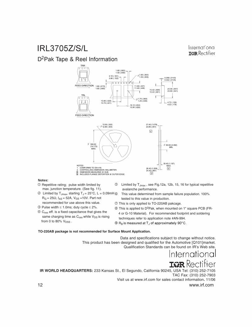
!
3
4
4
TRR
FEED DIRECTION
1.85 (.073)1.65 (.065)
1.60 (.063)1.50 (.059)
4.10 (.161)3.90 (.153)
TRL
FEED DIRECTION
10.90 (.429)10.70 (.421)
16.10 (.634)15.90 (.626)
1.75 (.069)1.25 (.049)
11.60 (.457)11.40 (.449)
15.42 (.609)15.22 (.601)
4.72 (.136)4.52 (.178)
24.30 (.957)23.90 (.941)
0.368 (.0145)0.342 (.0135)
1.60 (.063)1.50 (.059)
13.50 (.532)12.80 (.504)
330.00(14.173) MAX.
27.40 (1.079)23.90 (.941)
60.00 (2.362) MIN.
30.40 (1.197) MAX.
26.40 (1.039)24.40 (.961)
NOTES :1. COMFORMS TO EIA-418.2. CONTROLLING DIMENSION: MILLIMETER.3. DIMENSION MEASURED @ HUB.4. INCLUDES FLANGE DISTORTION @ OUTER EDGE.

Note: For the most current drawings please refer to the IR website at: http://www.irf.com/package/
![{i[t iHffi iH i .x g. ]J $t*t ilx fl j t;*{ r*:t esztendo 3 resz.pdf · g #:$ #,H Hg*h* S#*'S n: f.'-f, ;{rSr8 lH"H H ti ',#_HSd-Hs h H H ils H E8€' #8e;-ta trff tn g ''; j' : q1](https://img.pdfslide.net/doc/110x75/5be4fb0e09d3f20a668d9b38/it-ihffi-ih-i-x-g-j-tt-ilx-fl-j-t-rt-esztendo-3-reszpdf-g-h.jpg)


![elid elhlciml.250x.com/archive/marx_engels/arabic/marx_class...4 \ ]» T Z U» T » ~ g W [ ¿ T j U T h P ~ . Y l U c Y L i T T h U g . g g ` T](https://img.pdfslide.net/doc/110x75/5e490c1ed194ec050954b454/elid-elhlciml250xcomarchivemarxengelsarabicmarxclass-4-t-z-u.jpg)