Embed Size (px)
Citation preview
PCA-6740ISA STPC Elite 133 Half-size CPU cardwith CPU/32MB SDRAM/VGA/LCD/LAN/DOC/CF/PC104
User’s Manual

Copyright notice
This document is copyrighted 2002, by Advantech Co., Ltd. All rightsare reserved. The original manufacturer reserves the right to makeimprovements to the products described in this manual at any timewithout notice.
No part of this manual may be reproduced, copied, translated ortransmitted in any form or by any means without the prior writtenpermission of the original manufacturer. Information provided in thismanual is intended to be accurate and reliable. However, the originalmanufacturer assumes no responsibility for its use, nor for anyinfringements upon the rights of third parties which may result fromits use.
Acknowledgments
Award is a trademark of Award Software International, Inc.IBM, PC/AT, PS/2 and VGA are trademarks of International BusinessMachines Corporation.Intel and Pentium are trademarks of Intel Corporation.Microsoft Windows® is a registered trademark of Microsoft Corp.UMC is a trademark of United Microelectronics Corporation.
All other product names or trademarks are properties of theirrespective owners.
For more information on this and other Advantech products pleasevisit our websites at: http://www.advantech.com
http://www.advantech.com/epc
For technical support and service for please visit our support websiteat: http://www.advantech.com/support
This manual is for the PCA-6740 series half-size CPU card.
Part No. 2006674011
2nd Edition Published in Taiwan Apr., 2002
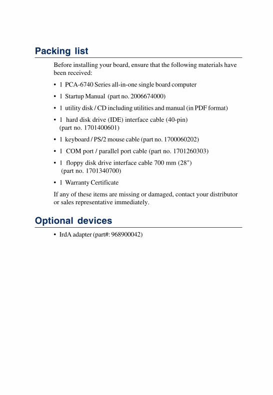
Packing listBefore installing your board, ensure that the following materials havebeen received:
• 1 PCA-6740 Series all-in-one single board computer
• 1 Startup Manual (part no. 2006674000)
• 1 utility disk / CD including utilities and manual (in PDF format)
• 1 hard disk drive (IDE) interface cable (40-pin)(part no. 1701400601)
• 1 keyboard / PS/2 mouse cable (part no. 1700060202)
• 1 COM port / parallel port cable (part no. 1701260303)
• 1 floppy disk drive interface cable 700 mm (28") (part no. 1701340700)
• 1 Warranty Certificate
If any of these items are missing or damaged, contact your distributoror sales representative immediately.
Optional devices• IrdA adapter (part#: 968900042)
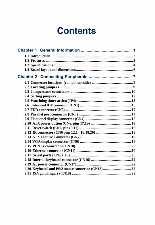
Contents
Chapter 1 General Information ............................................ 11.1 Introduction....................................................................................... 21.2 Features ............................................................................................ 31.3 Specifications .................................................................................... 41.4 Board layout and dimensions ............................................................ 6
Chapter 2 Connecting Peripherals ..................................... 72.1 Connector locations (component side) ............................................ 82.2 Locating jumpers .............................................................................. 92.3 Jumpers and connectors ................................................................ 102.4 Setting jumpers .............................................................................. 122.5 Watchdog timer action (JP4) .......................................................... 152.6 Enhanced IDE connector (CN1) ...................................................... 162.7 FDD connector (CN2) ..................................................................... 172.8 Parallel port connector (CN3) ........................................................ 172.9 Flat panel display connector (CN4) ................................................ 182.10 ATX power button (CN6, pins 17,19) ........................................... 182.11 Reset switch (CN6, pins 9,11) ....................................................... 182.12 IR connector (CN6 pins 12,14,16,18,20) ..................................... 182.13 ATX Feature Connector (CN7) .................................................... 192.14 VGA display connector (CN9) ...................................................... 192.15 PC/104 connectors (CN10) .......................................................... 202.16 Ethernet connector (CN11) .......................................................... 202.17 Serial ports (CN13~15) ................................................................ 202.18 Internal keyboard connector (CN16) ........................................... 222.19 AT power connector (CN17) ......................................................... 222.20 Keyboard and PS/2 mouse connector (CN18) .............................. 222.21 ISA gold fingers (CN19) .............................................................. 22
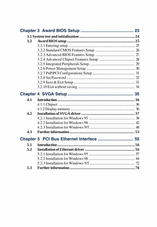
Chapter 3 Award BIOS Setup ............................................. 233.1 System test and initialization .......................................................... 243.2 Award BIOS setup ....................................................................... 25
3.2.1 Entering setup ..................................................................... 253.2.2 Standard CMOS Features Setup ......................................... 263.2.3 Advanced BIOS Features Setup ......................................... 273.2.4 Advanced Chipset Features Setup ..................................... 283.2.5 Integrated Peripherals Setup ............................................... 293.2.6 Power Management Setup .................................................. 303.2.7 PnP/PCI Configurations Setup ............................................ 313.2.8 Set Password ....................................................................... 323.2.9 Save & Exit Setup ................................................................ 333.2.10 Exit without saving ............................................................ 34
Chapter 4 SVGA Setup ........................................................ 354.1 Introduction................................................................................. 36
4.1.1 Chipset ................................................................................ 364.1.2 Display memory ................................................................... 36
4.2 Installation of SVGA driver ........................................................ 374.2.1 Installation for Windows 95 ................................................ 384.2.2 Installation for Windows 98 ................................................ 424.2.3 Installation for Windows NT ............................................... 48
4.3 Further information .................................................................... 53
Chapter 5 PCI Bus Ethernet Interface .............................. 555.1 Introduction................................................................................. 565.2 Installation of Ethernet driver .................................................... 56
5.2.1 Installation for Windows 95 ................................................ 575.2.2 Installation for Windows 98 ................................................ 645.2.3 Installation for Windows NT ............................................... 72
5.3 Further information .................................................................... 76
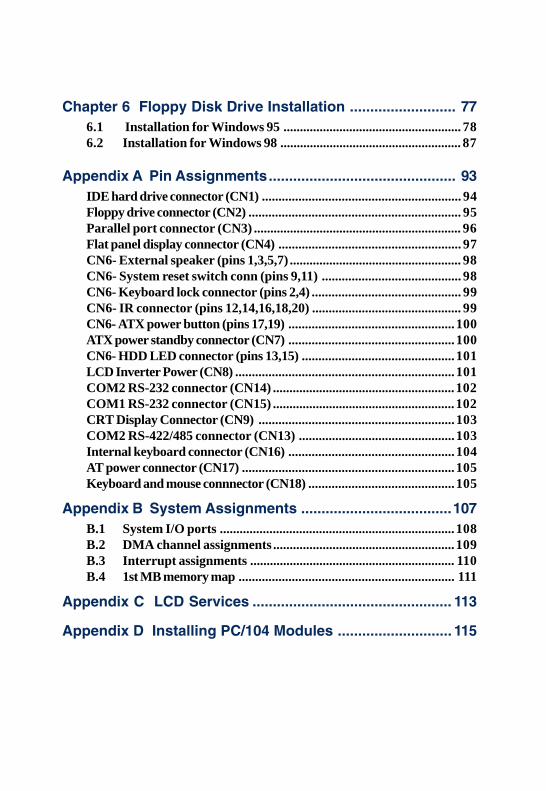
Chapter 6 Floppy Disk Drive Installation .......................... 776.1 Installation for Windows 95 ...................................................... 786.2 Installation for Windows 98 ....................................................... 87
Appendix A Pin Assignments.............................................. 93IDE hard drive connector (CN1) ............................................................ 94Floppy drive connector (CN2) ................................................................ 95Parallel port connector (CN3) ............................................................... 96Flat panel display connector (CN4) ....................................................... 97CN6- External speaker (pins 1,3,5,7) .................................................... 98CN6- System reset switch conn (pins 9,11) .......................................... 98CN6- Keyboard lock connector (pins 2,4) ............................................. 99CN6- IR connector (pins 12,14,16,18,20) ............................................. 99CN6- ATX power button (pins 17,19) ..................................................100ATX power standby connector (CN7) ..................................................100CN6- HDD LED connector (pins 13,15) ..............................................101LCD Inverter Power (CN8) ..................................................................101COM2 RS-232 connector (CN14) .......................................................102COM1 RS-232 connector (CN15) .......................................................102CRT Display Connector (CN9) ...........................................................103COM2 RS-422/485 connector (CN13) ...............................................103Internal keyboard connector (CN16) ..................................................104AT power connector (CN17) ................................................................105Keyboard and mouse connnector (CN18) ............................................105
Appendix B System Assignments .....................................107B.1 System I/O ports .......................................................................108B.2 DMA channel assignments .......................................................109B.3 Interrupt assignments .............................................................. 110B.4 1st MB memory map ................................................................. 111
Appendix C LCD Services ................................................. 113
Appendix D Installing PC/104 Modules ............................ 115
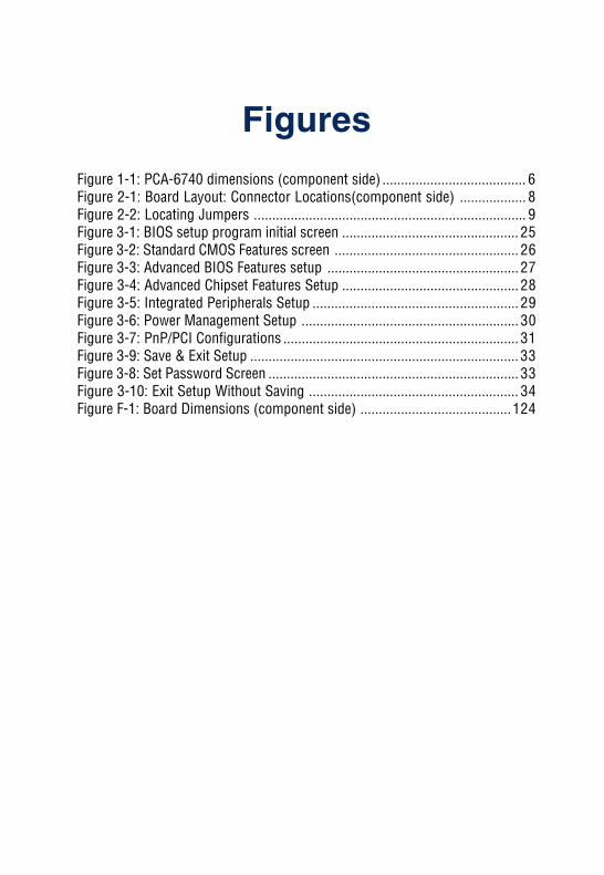
Figures
Figure 1-1: PCA-6740 dimensions (component side) ....................................... 6Figure 2-1: Board Layout: Connector Locations(component side) .................. 8Figure 2-2: Locating Jumpers .......................................................................... 9Figure 3-1: BIOS setup program initial screen ................................................ 25Figure 3-2: Standard CMOS Features screen .................................................. 26Figure 3-3: Advanced BIOS Features setup .................................................... 27Figure 3-4: Advanced Chipset Features Setup ................................................ 28Figure 3-5: Integrated Peripherals Setup ........................................................ 29Figure 3-6: Power Management Setup ........................................................... 30Figure 3-7: PnP/PCI Configurations ................................................................ 31Figure 3-9: Save & Exit Setup ......................................................................... 33Figure 3-8: Set Password Screen .................................................................... 33Figure 3-10: Exit Setup Without Saving ......................................................... 34Figure F-1: Board Dimensions (component side) .........................................124
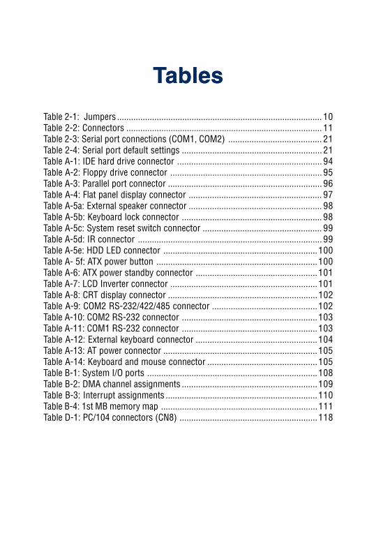
TablesTables
Table 2-1: Jumpers ........................................................................................ 10Table 2-2: Connectors .................................................................................... 11Table 2-3: Serial port connections (COM1, COM2) ........................................ 21Table 2-4: Serial port default settings ............................................................ 21Table A-1: IDE hard drive connector .............................................................. 94Table A-2: Floppy drive connector ................................................................. 95Table A-3: Parallel port connector .................................................................. 96Table A-4: Flat panel display connector ......................................................... 97Table A-5a: External speaker connector ......................................................... 98Table A-5b: Keyboard lock connector ............................................................ 98Table A-5c: System reset switch connector ................................................... 99Table A-5d: IR connector ............................................................................... 99Table A-5e: HDD LED connector ..................................................................100Table A- 5f: ATX power button .....................................................................100Table A-6: ATX power standby connector ....................................................101Table A-7: LCD Inverter connector ...............................................................101Table A-8: CRT display connector ................................................................102Table A-9: COM2 RS-232/422/485 connector .............................................102Table A-10: COM2 RS-232 connector ..........................................................103Table A-11: COM1 RS-232 connector ..........................................................103Table A-12: External keyboard connector ....................................................104Table A-13: AT power connector ..................................................................105Table A-14: Keyboard and mouse connector ...............................................105Table B-1: System I/O ports .........................................................................108Table B-2: DMA channel assignments ..........................................................109Table B-3: Interrupt assignments .................................................................110Table B-4: 1st MB memory map ...................................................................111Table D-1: PC/104 connectors (CN8) ...........................................................118
CH
AP
TE
R
General Information
This chapter gives background informa-tion on the PCA-6740.
Sections include:
• Board specifications
• Board layout and dimensions
1
2 PCA-6740 User's Manual
1.1 IntroductionThe PCA-6740 is the ultimate cost-effective solution for limited-space applications. It offers all the functions of an AT-compatibleindustrial computer on a single board. The PCA-6740 comes withan embedded high-performance STPC Elite 133 processor and32MB SDRAM on board. For maximum performance, the PCA-6740also supports one optional SODIMM socket that can accept up to64 MB memory.
On-board features include an Ethernet interface, a socket for DOC®
2000, Enhanced IDE interface, one parallel port, two serial ports(RS-232 and RS-232/422/485) with DB-9 connector as COM1, and amini-DIN PS/2 keyboard/mouse interface. An SVGA/LCD displaycontroller (LCD, and CRT displays) allows LCD screen resolutionsup to 1024 x 768 @ 64K colors and CRT resolutions up to 1280 x1024 @ 256 colors.
The PCA-6740 complies with the "Green Function" standard andsupports three types of power saving features: Normal, Doze andSleep modes.
The display type configuration is done through software. A singleFlash chip holds the system BIOS and the VGA BIOS. Thisminimizes the number of chips and eases configuration. You canchange the display BIOS simply by programming the Flash chip.
If you need any additional functions, the PCA-6740 has a PC/104connector for future upgrades.
Chapter 1 General Information 3
1.2 Features• On-board Low power STMicroelectronics STPC Elite 133
processor (fanless)
• On-board 32 MB SDRAM
• On-board VGA/LCD display controller and 18-bit LCD TFTdisplay
• 62-level watchdog timer, jumperless on-line setup supported
• Supports wake-up on LAN, ring-on by Modem
• SSD supports DiskOnChip® 2000
• Supports CMOS data backup functions
• PC/104 connector supports face-up installation
4 PCA-6740 User's Manual
1.3 Specifications
1.3.1 Standard SBC functions
• CPU: Embedded STMicroelectronics STPC Elite 133 MHzprocessor (provides fanless operation)
• BIOS: 4 Mbit Flash BIOS,-Supports Plug & Play, APM-Supports Ethernet Boot ROM-Supports boot from CD-ROM-Supports boot from LS-120 ZIP™ Drive-Optional Customer icon can be supplied
• Chipset: STPC Elite 133
• System memory: Onboard 32MB SDRAM, and one optional SDRAM SODIMM max. 64MB socket
• PCI IDE interface: One Enhanced IDE interface. Supports 2 IDEdevices PIO mode 3,4 with bus mastering up to 14 MB/sec.
• Floppy disk drive interface: Supports up to two FDDs (360 KB/1.2 MB/720 KB/1.44 MB/2.88 MB)
• Parallel port: One parallel port, supports EPP/ECP
• IR port: One 115 kbps IrDA compliant serial infrared
• Serial ports: 2 serial ports COM1: RS-232, COM2: RS-232/422/485
• Watchdog timer: 62-level timer interval, setup by software orjumperless selection, generates system reset or IRQ11.
Chapter 1 General Information 5
1.3.2 Local-bus flat panel/VGA interface
• Chipset: SMI LynxEM+ 712G
• Display memory: 2MB
• Display type: Simultaneous support for CRT and 18-bit TFT LCDdisplay (supports 3.3 V and 5 V LCD)
• Resolution: Non-interlaced CRT monitor resolution up to 1280 x1024 @ 256 colors, Panel resolutions up to 1024 x 768 @ 64Kcolors TFT panel
1.3.3 Ethernet interface
• Chipset: RTL 8139C
• Ethernet interface: PCI 10/100 Mbps Ethernet. IEEE 802.3 uprotocol compatible
• Connection: On-board RJ-45 connector
• I/O address switchless setting
• Built-in boot ROM
1.3.4 Mechanical and environmental
• Dimensions (L x W): 185 mm x 122 mm
• Power supply voltage: +5 V (4.75 ~ 5.25 V)
• Power consumption :- Maximum: 5 V @ 2 A
Typical: +5 V @ 1.62 A
• Operating temperature: 0 ~ 60° C (32 ~ 140° F)
• Weight: 0.27 kg (0.59 lbs)
1.3.5 Solid state disk
• Provides support for one DOC® 2000.
6 PCA-6740 User's Manual
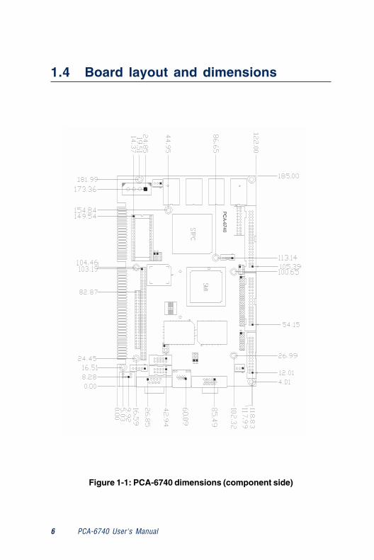
1.4 Board layout and dimensions
Figure 1-1: PCA-6740 dimensions (component side)
Chapter 2 Connecting 7
CH
AP
TE
R
2ConnectingPeripheralsThis chapter tells how to connectperipherals, switches and indicators to thePCA-6740 board. You can access most ofthe connectors from the top of the boardwhile it is installed in the chassis. If youhave a number of cards installed, or yourchassis is very tight, you may need topartially remove the card to make all theconnections.
8 PCA-6740 User's Manual
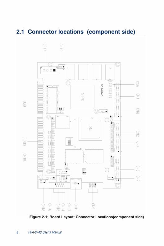
2.1 Connector locations (component side)
Figure 2-1: Board Layout: Connector Locations(component side)
Chapter 2 Connecting 9
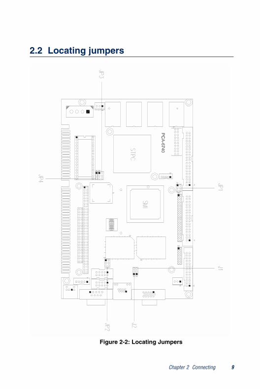
2.2 Locating jumpers
Figure 2-2: Locating Jumpers
10 PCA-6740 User's Manual
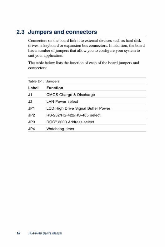
2.3 Jumpers and connectorsConnectors on the board link it to external devices such as hard diskdrives, a keyboard or expansion bus connectors. In addition, the boardhas a number of jumpers that allow you to configure your system tosuit your application.
The table below lists the function of each of the board jumpers andconnectors:
Table 2-1: Jumpers
Label Function
J1 CMOS Charge & Discharge
J2 LAN Power select
JP1 LCD High Drive Signal Buffer Power
JP2 RS-232/RS-422/RS-485 select
JP3 DOC® 2000 Address select
JP4 Watchdog timer
Chapter 2 Connecting 11
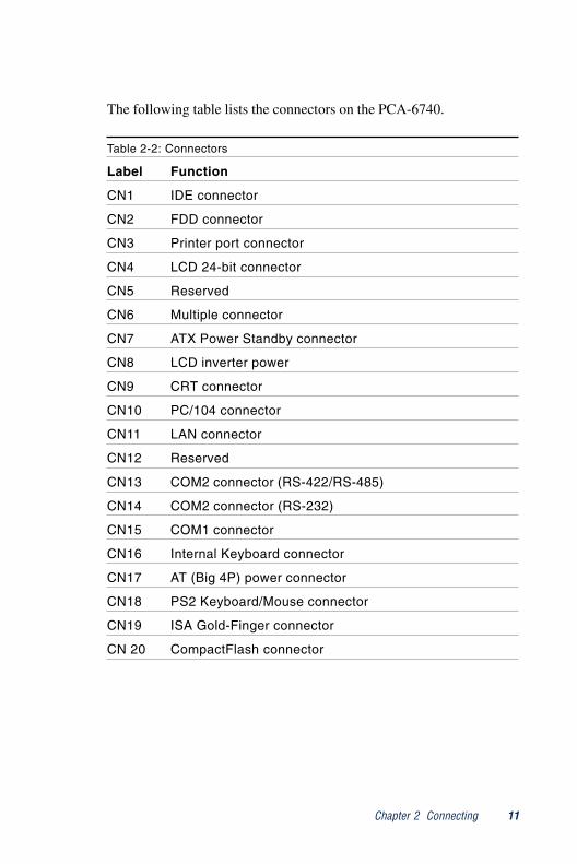
The following table lists the connectors on the PCA-6740.
Table 2-2: Connectors
Label Function
CN1 IDE connector
CN2 FDD connector
CN3 Printer port connector
CN4 LCD 24-bit connector
CN5 Reserved
CN6 Multiple connector
CN7 ATX Power Standby connector
CN8 LCD inverter power
CN9 CRT connector
CN10 PC/104 connector
CN11 LAN connector
CN12 Reserved
CN13 COM2 connector (RS-422/RS-485)
CN14 COM2 connector (RS-232)
CN15 COM1 connector
CN16 Internal Keyboard connector
CN17 AT (Big 4P) power connector
CN18 PS2 Keyboard/Mouse connector
CN19 ISA Gold-Finger connector
CN 20 CompactFlash connector
12 PCA-6740 User's Manual
2.4 Setting jumpers
2.4.1 Introduction
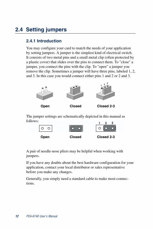
You may configure your card to match the needs of your applicationby setting jumpers. A jumper is the simplest kind of electrical switch.It consists of two metal pins and a small metal clip (often protected bya plastic cover) that slides over the pins to connect them. To "close" ajumper, you connect the pins with the clip. To "open” a jumper youremove the clip. Sometimes a jumper will have three pins, labeled 1, 2,and 3. In this case you would connect either pins 1 and 2 or 2 and 3.
A pair of needle-nose pliers may be helpful when working withjumpers.
If you have any doubts about the best hardware configuration for yourapplication, contact your local distributor or sales representativebefore you make any changes.
Generally, you simply need a standard cable to make most connec-tions.
13
2
Closed 2-3Open Closed
Closed 2-3Open Closed
1 2 3321
The jumper settings are schematically depicted in this manual asfollows:
Chapter 2 Connecting 13
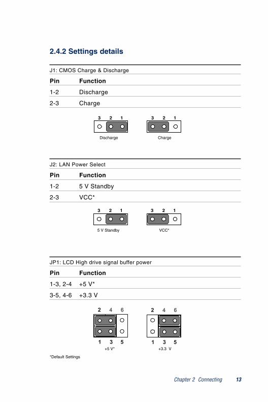
J2: LAN Power Select
Pin Function
1-2 5 V Standby
2-3 VCC*
2.4.2 Settings details
J1: CMOS Charge & Discharge
Pin Function
1-2 Discharge
2-3 Charge
JP1: LCD High drive signal buffer power
Pin Function
1-3, 2-4 +5 V*
3-5, 4-6 +3.3 V
*Default Settings
3 2 1 3 2 1
Discharge Charge
3 2 1 3 2 1
5 V Standby VCC*
+5 V* +3.3 V
14 PCA-6740 User's Manual
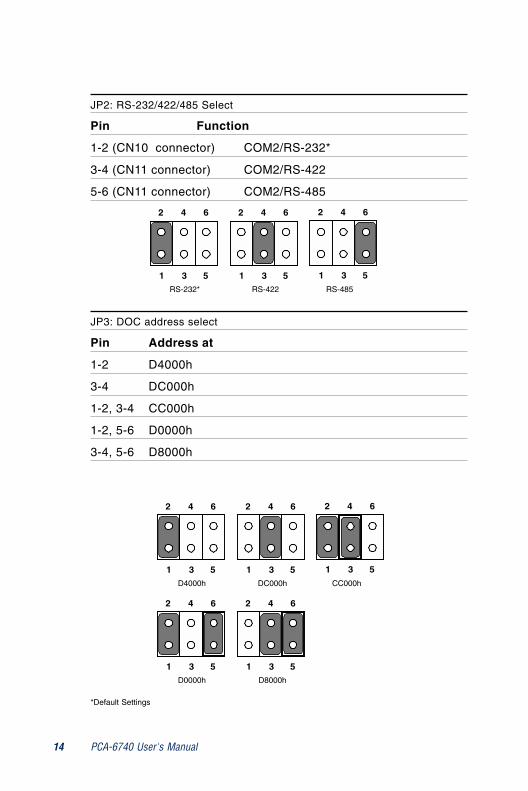
JP2: RS-232/422/485 Select
Pin Function
1-2 (CN10 connector) COM2/RS-232*
3-4 (CN11 connector) COM2/RS-422
5-6 (CN11 connector) COM2/RS-485
JP3: DOC address select
Pin Address at
1-2 D4000h
3-4 DC000h
1-2, 3-4 CC000h
1-2, 5-6 D0000h
3-4, 5-6 D8000h
2 4 6
1 3 5
2 4 6
1 3 5
2 4 6
1 3 5
RS-232* RS-422 RS-485
2 4 6
1 3 5
2 4 6
1 3 5D4000h DC000h CC000h
2 4 6
1 3 5
2 4 6
1 3 5D0000h D8000h
*Default Settings
2 4 6
1 3 5
Chapter 2 Connecting 15
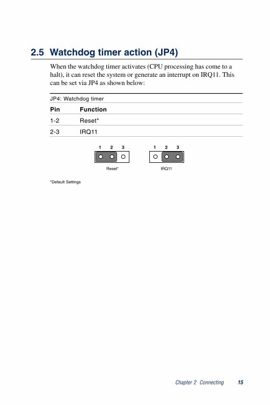
2.5 Watchdog timer action (JP4)When the watchdog timer activates (CPU processing has come to ahalt), it can reset the system or generate an interrupt on IRQ11. Thiscan be set via JP4 as shown below:
JP4: Watchdog timer
Pin Function
1-2 Reset*
2-3 IRQ11
1 2 3 1 2 3
Reset* IRQ11
*Default Settings
16 PCA-6740 User's Manual
The following sections tell how to make each connection. In mostcases, you will simply need to connect a standard cable. All of theconnector pin assignments are shown in Appendix A.
Warning! Always completely disconnect the power cord fromyour chassis whenever you are working on it. Do notmake connections while the power is on. Sensitiveelectronic components can be damaged by asudden rush of power. Only experienced electronicspersonnel should open the PC chassis.
Caution! Always ground yourself to remove any static chargebefore touching the CPU card. Modern electronicdevices are very sensitive to static electric charges.Use a grounding wrist strap at all times. Place allelectronic components on a static-dissipativesurface or in a static-shielded bag when they are notin the chassis.
2.6 Enhanced IDE connector (CN1)You can attach two IDE (Integrated Device Electronics) drives to thePCA-6740 internal controller. The PCA-6740 CPU card has an EIDEconnector, CN1.
Wire number 1 on the cable is red or blue, and the other wires are gray.Connect one end to connector CN1 on the CPU card. Make sure thatthe red (or blue) wire corresponds to pin 1 on the connector. SeeFigure 2-1, where pin 1 is indicated with a triangle and a solid square.
Unlike floppy drives, IDE hard drives can connect in either position onthe cable. If you install two drives, you will need to set one as themaster and one as the slave. You do this by setting the jumpers on thedrives. If you use just one drive, you should set it as the master. Seethe documentation that came with your drive for more information.
Connect the first hard drive to the other end of the cable. Wire 1 on thecable should also connect to pin 1 on the hard drive connector, whichshould be labeled on the drive circuit board. Check the documentationthat came with the drive for more information. If you are using asecond drive, connect it to the remaining connector on the same cable.
Chapter 2 Connecting 17
2.7 FDD connector (CN2)You can attach up to two floppy disk drives to the PCA-6740'sonboard controller. You can use any combination of 5.25" (360 KB/1.2 MB) and/or 3.5" (720 KB/1.44/2.88 MB) drives.
The card comes with a 34-pin daisy-chain drive connector cable. Onone end of the cable is a 34-pin flat-cable connector. On the other endare two sets of floppy disk drive connectors. Each set consists of a 34-pin flat-cable connector (usually used for 3.5" drives) and a printed-circuit-board connector (usually used for 5.25" drives). You can useonly one connector in each set. The set on the end (after the twist inthe cable) connects to the A: floppy. The set in the middle connects tothe B: floppy.
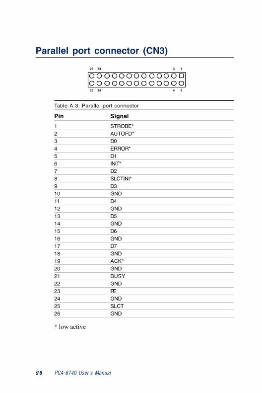
2.8 Parallel port connector (CN3)The parallel port is designated as LPT1, and is normally used toconnect the CPU card to a printer. The PCA-6740 includes an on-board parallel port, accessed through a 26-pin flat-cable connector,CN3. The card comes with an adapter cable which lets you use atraditional DB-25 connector. The cable has a 26-pin connector on oneend and a DB-25 connector on the other, mounted on a retainingbracket. The bracket installs at the end of an empty slot in yourchassis, giving you access to the connector.
To install the bracket, find an empty slot in your chassis. Unscrew theplate that covers the end of the slot. Screw in the bracket in place ofthe plate. Next, attach the flat-cable connector to CN3 on the CPUcard. Wire 1 of the cable is red or blue, and the other wires are gray.Make sure that wire 1 corresponds to pin 1 of CN3. Pin 1 is on theright side of CN3.
18 PCA-6740 User's Manual
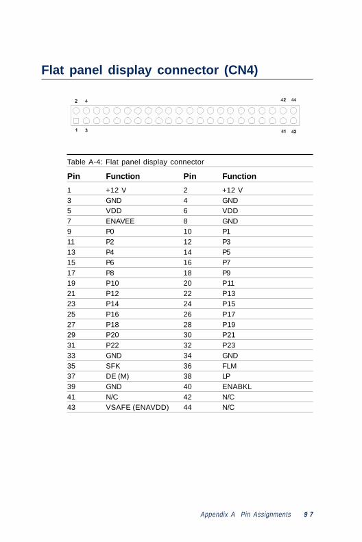
2.9 Flat panel display connector (CN4)CN4 consists of a 44-pin, dual-in-line header.
The power supply (+12 V) for CN4 is dependant on the supplyconnected to the board. Therefore make sure that CN17 is connectedto a +12 V power supply.
The PCA-6740 provides a bias control signal on CN4 which can beused to control the LCD bias voltage. It is recommended that the LCDbias voltage not be applied to the panel until the logic supply voltage(+5 V or +3.3 V) and panel video signals are stable. Under normaloperation the control signal (ENAVEE) is active high. When the PCA-6740 board's power is applied, the control signal is low until just afterthe relevant flat panel signals are present.
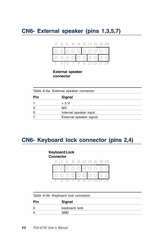
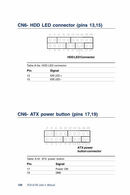
2.10 ATX power button (CN6, pins 17,19)The PCA-6740 provides an ATX power input connector. Whenconnected with the ATX power switch, the ATX power switch connec-tor (CN6) enables power On/Off from the chassis.
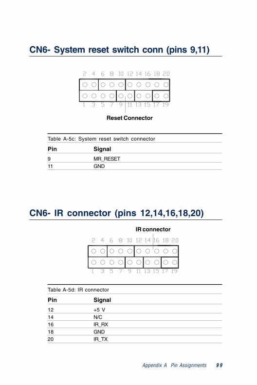
2.11 Reset switch (CN6, pins 9,11)If you install a reset switch, it should be a single pole switch rated at10 mA, 5 V. Momentarily pressing the switch will activate a reset.
For reset switch pin assignments, please see Appendix A.
2.12 IR connector (CN6 pins 12,14,16,18,20)This connector supports the optional wireless infrared transmitting andreceiving module. This module mounts on the system case. You mustconfigure the setting through BIOS setup.
Chapter 2 Connecting 19
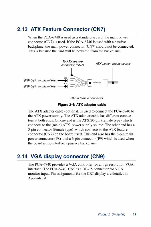
2.13 ATX Feature Connector (CN7)When the PCA-6740 is used as a standalone card, the main powerconnector (CN7) is used. If the PCA-6740 is used with a passivebackplane, the main power connector (CN7) should not be connected.This is because the card will be powered from the backplane.
Figure 2-4: ATX adaptor cable
The ATX adapter cable (optional) is used to connect the PCA-6740 tothe ATX power supply. The ATX adapter cable has different connec-tors at both ends. On one end is the ATX 20-pin (female type) whichconnects to the (male) ATX power supply source. The other end has a3-pin connector (female type) which connects to the ATX featureconnector (CN7) on the board itself. This end also has the 6-pin mainpower connector (P8) and a 6-pin connector (P9) which is used whenthe board is mounted on a passive backplane.
P9
P8
P9
P8
(P8) 6-pin in backplane
(P9) 6-pin in backplane
ATX power supply source
20-pin female connector
To ATX featureconnector (CN7)
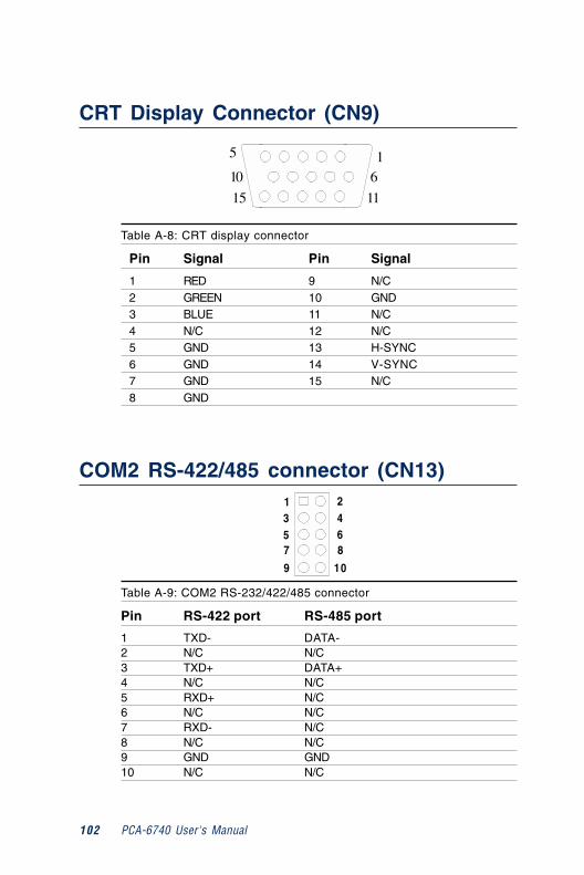
2.14 VGA display connector (CN9)The PCA-6740 provides a VGA controller for a high resolution VGAinterface. The PCA-6740 CN9 is a DB-15 connector for VGAmonitor input. Pin assignments for the CRT display are detailed inAppendix A.
20 PCA-6740 User's Manual
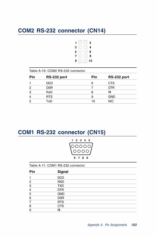
2.17 Serial ports(CN15: COM1; CN14: COM2/RS-232; CN13: COM2/RS-422/485)
The PCA-6740 offers two serial ports: COM1 in RS-232 and COM2(CN14: RS-232, CN13:RS-422/485). These ports let you connect toserial devices (a mouse, printers, etc.) or a communication network.
You can select the address for each port (for example, 3F8H [COM1],2F8H [COM2]) or disable each port. Use the BIOS Advanced Setupprogram, which is covered in Chapter 4.
The card mounting bracket holds the serial port connector for the oneport. The parallel port and serial port adapter kit (supplied with thecard) holds the connector for the other port. This lets you connect anddisconnect cables after you install the card. The DB-9 connector on thebottom of the bracket is the first RS-232 port, COM1. The DB-9connector on the adapter kit is the second serial port, COM2.
2.15 PC/104 connectors (CN10)The PCA-6740 is equipped with a 16-bit ISA signal PC/104 connectorfor future expansion. See Appendix D for details.
2.16 Ethernet connector (CN11)The PCA-6740 is equipped with a high performance 32-bit PCI-busFast Ethernet interface which is fully compliant with IEEE 802.3u10/100Base-T specifications. It is supported by all major networkoperating systems.
The medium type can be configured via the rset8139.EXE programincluded on the utility disk. (See Chapter 5 for detailed information.)
2.16.1 Network bootThe network boot feature is built into the BIOS. It can be enabled ordisabled in the chipset setup of the CMOS configuration. Refer to"BIOS Setting" in Chapter 4 for more information.
Chapter 2 Connecting 21
2.17.1 RS-232 connection (COM1:CN15)
Different devices implement the RS-232 standard in different ways. Ifyou are having problems with a serial device, be sure to check the pinassignments for the connector.
2.17.2 RS-232/422/485 connection (COM2: CN10: RS-232; CN11: RS-422/485)
COM2 is an RS-232/422/485 serial port. The specific port type isdetermined by jumper settings (JP2), as detailed in Chapter 1.
The IRQ and address range for both ports are fixed. However, if youwish to disable the port or change these parameters later, you can dothis in the system BIOS setup. The table below shows the settings forthe PCA-6740 series' board's ports:
Table 2-4: Serial port default settings
Port Address Interrupt Default
COM1 3F8, 3E8 IRQ4 3F8
COM2 2F8, 2E8 IRQ3 2F8
Table 2-3: Serial port connections (COM1, COM2)
Connector Function
COM1,3*,4* RS-232
COM2 RS-232/422/485
22 PCA-6740 User's Manual
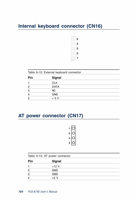
2.18 Internal keyboard connector (CN16)In addition to the PS/2 mouse/keyboard connector, an additionalexternal keyboard connector is provided.
For external keyboard pin assignments, see Appendix A.
2.19 AT power connector (CN17)If you prefer not to acquire power through the PCA-6740 backplanevia the gold H-connectors, The big 4P power connector (CN17) alsoprovides power input connectors for +5 V, and +12 V.
2.20 Keyboard and PS/2 mouse connector (CN18)The PCA-6740 board provides a keyboard connector. A 6-pin mini-DIN connector (CN18) on the card mounting bracket supports single-board computer applications. The card comes with an adapter toconvert from the 6-pin mini-DIN connector to a standard DIN connec-tor and to a PS/2 mouse connector.
2.21 ISA gold fingers (CN19)The 16-bit ISA gold fingers are used for connecting the PCA-6740Series to an ISA passive backplane.
Award BIOS SetupThis chapter describes how to set BIOSconfiguration data.
CH
AP
TE
R
3
24 PCA-6753 User's Manual
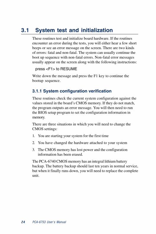
3.1 System test and initializationThese routines test and initialize board hardware. If the routinesencounter an error during the tests, you will either hear a few shortbeeps or see an error message on the screen. There are two kindsof errors: fatal and non-fatal. The system can usually continue theboot up sequence with non-fatal errors. Non-fatal error messagesusually appear on the screen along with the following instructions:
press <F1> to RESUME
Write down the message and press the F1 key to continue thebootup sequence.
3.1.1 System configuration verification
These routines check the current system configuration against thevalues stored in the board’s CMOS memory. If they do not match,the program outputs an error message. You will then need to runthe BIOS setup program to set the configuration information inmemory.
There are three situations in which you will need to change theCMOS settings:
1. You are starting your system for the first time
2. You have changed the hardware attached to your system
3. The CMOS memory has lost power and the configurationinformation has been erased.
The PCA-6740 CMOS memory has an integral lithium batterybackup. The battery backup should last ten years in normal service,but when it finally runs down, you will need to replace the completeunit.
Chapter 3 Award BIOS Setup 25
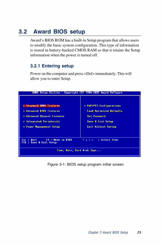
3.2 Award BIOS setupAward’s BIOS ROM has a built-in Setup program that allows usersto modify the basic system configuration. This type of informationis stored in battery-backed CMOS RAM so that it retains the Setupinformation when the power is turned off.
3.2.1 Entering setup
Power on the computer and press <Del> immediately. This willallow you to enter Setup.
Figure 3-1: BIOS setup program initial screen
26 PCA-6753 User's Manual
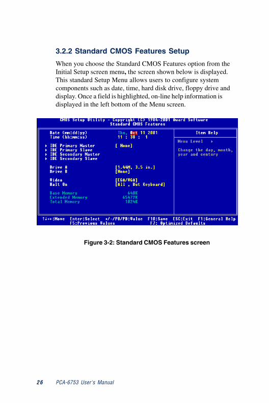
3.2.2 Standard CMOS Features Setup
When you choose the Standard CMOS Features option from theInitial Setup screen menu, the screen shown below is displayed.This standard Setup Menu allows users to configure systemcomponents such as date, time, hard disk drive, floppy drive anddisplay. Once a field is highlighted, on-line help information isdisplayed in the left bottom of the Menu screen.
Figure 3-2: Standard CMOS Features screen
Chapter 3 Award BIOS Setup 27
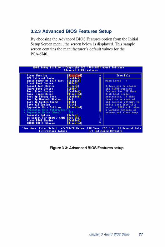
3.2.3 Advanced BIOS Features Setup
By choosing the Advanced BIOS Features option from the InitialSetup Screen menu, the screen below is displayed. This samplescreen contains the manufacturer’s default values for thePCA-6740.
Figure 3-3: Advanced BIOS Features setup
28 PCA-6753 User's Manual
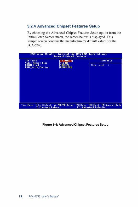
3.2.4 Advanced Chipset Features Setup
By choosing the Advanced Chipset Features Setup option from theInitial Setup Screen menu, the screen below is displayed. Thissample screen contains the manufacturer’s default values for thePCA-6740.
Figure 3-4: Advanced Chipset Features Setup
Chapter 3 Award BIOS Setup 29
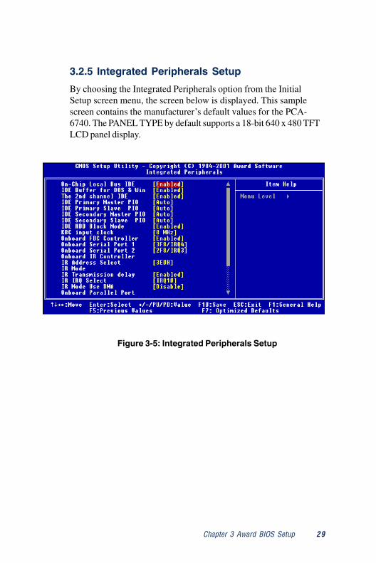
3.2.5 Integrated Peripherals Setup
By choosing the Integrated Peripherals option from the InitialSetup screen menu, the screen below is displayed. This samplescreen contains the manufacturer’s default values for the PCA-6740. The PANEL TYPE by default supports a 18-bit 640 x 480 TFTLCD panel display.
Figure 3-5: Integrated Peripherals Setup
30 PCA-6753 User's Manual
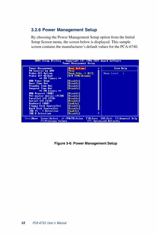
3.2.6 Power Management Setup
By choosing the Power Management Setup option from the InitialSetup Screen menu, the screen below is displayed. This samplescreen contains the manufacturer’s default values for the PCA-6740.
Figure 3-6: Power Management Setup
Chapter 3 Award BIOS Setup 31
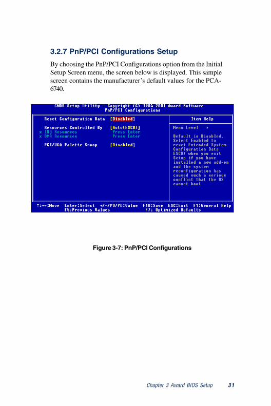
3.2.7 PnP/PCI Configurations Setup
By choosing the PnP/PCI Configurations option from the InitialSetup Screen menu, the screen below is displayed. This samplescreen contains the manufacturer’s default values for the PCA-6740.
Figure 3-7: PnP/PCI Configurations
32 PCA-6753 User's Manual
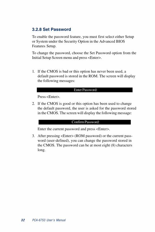
3.2.8 Set Password
To enable the password feature, you must first select either Setupor System under the Security Option in the Advanced BIOSFeatures Setup.
To change the password, choose the Set Password option from theInitial Setup Screen menu and press <Enter>.
1. If the CMOS is bad or this option has never been used, adefault password is stored in the ROM. The screen will displaythe following messages:
Enter Password:
Press <Enter>.
2. If the CMOS is good or this option has been used to changethe default password, the user is asked for the password storedin the CMOS. The screen will display the following message:
Confirm Password:
Enter the current password and press <Enter>.
3. After pressing <Enter> (ROM password) or the current pass-word (user-defined), you can change the password stored inthe CMOS. The password can be at most eight (8) characterslong.
Chapter 3 Award BIOS Setup 33
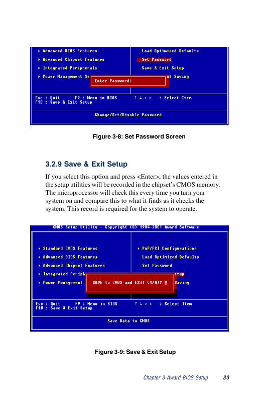
3.2.9 Save & Exit Setup
If you select this option and press <Enter>, the values entered inthe setup utilities will be recorded in the chipset’s CMOS memory.The microprocessor will check this every time you turn yoursystem on and compare this to what it finds as it checks thesystem. This record is required for the system to operate.
Figure 3-8: Set Password Screen
Figure 3-9: Save & Exit Setup
34 PCA-6753 User's Manual
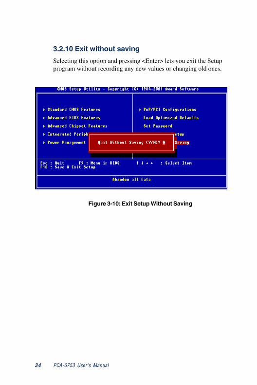
3.2.10 Exit without saving
Selecting this option and pressing <Enter> lets you exit the Setupprogram without recording any new values or changing old ones.
Figure 3-10: Exit Setup Without Saving

SVGA Setup• Introduction
• Installation of SVGA driver for Win-dows 95/98/NT4.0
CH
AP
TE
R
4
36 PCA-6740 User's Manual
4.1 IntroductionThe PCA-6740 has an on-board LCD/VGA interface. The specifica-tions and features are described as follows:
4.1.1 Chipset
The PCM-6740 uses a SMI LynxEM+ 712G chipset for its SVGAcontroller. It supports many popular 18-bit LCD displays andconventional analog CRT monitors. The VGA BIOS supports LCD.In addition, it also supports interlaced and non-interlaced analogmonitors (color and monochrome VGA) in high-resolution modeswhile maintaining complete IBM VGA compatibility. Digitalmonitors (i.e. MDA, CGA, and EGA) are NOT supported. Multiplefrequency (multisync) monitors are handled as if they were analogmonitors.
4.1.2 Display memory
With 2MB shared memory, the VGA controller can drive CRTdisplays or color panel displays with resolutions up to 1280 x 1024at 256 colors.
Chapter 4 SVGA Setup 37
4.2 Installation of SVGA driverComplete the following steps to install the SVGA driver. Follow theprocedures in the flow chart that apply to the operating system thatyou are using within your PCM-6740.
Important: The following windows illustrations are examplesonly. You must follow the flow chart instructionsand pay attention to the instructions which thenappear on your screen.
Note 1: The CD-ROM drive is designated as "D:" through-out this chapter.
Note 2: <Enter> means pressing the “Enter” key on thekeyboard.
Note 3: When you are using a CRT display, please makesure that your flat panel resolution settings (in theBIOS setup) are the same as your VGA resolutionsettings (in Windows). Otherwise your display maybehave strangely.
38 PCA-6740 User's Manual
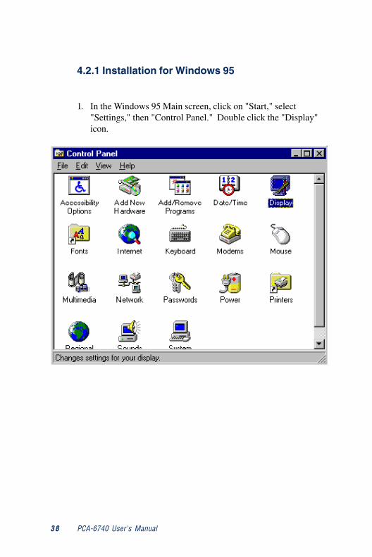
4.2.1 Installation for Windows 95
1. In the Windows 95 Main screen, click on "Start," select"Settings," then "Control Panel." Double click the "Display"icon.
Chapter 4 SVGA Setup 39
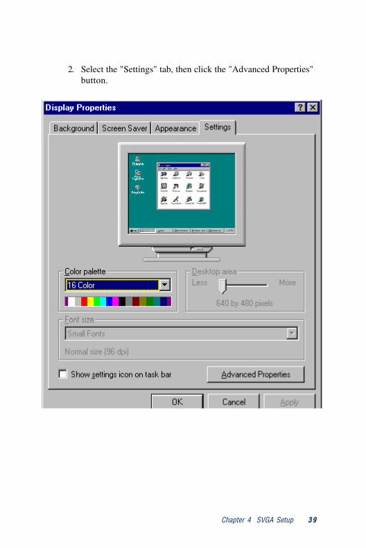
2. Select the "Settings" tab, then click the "Advanced Properties"button.
40 PCA-6740 User's Manual
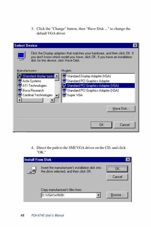
3. Click the "Change" button, then "Have Disk ..." to change thedefault VGA driver.
4. Direct the path to the SMI VGA driver on the CD, and click"OK."

Chapter 4 SVGA Setup 41
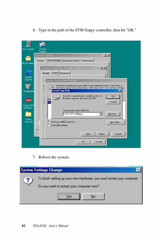
5. Select "Yes" to reboot the system.
42 PCA-6740 User's Manual
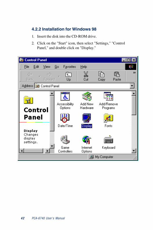
4.2.2 Installation for Windows 98
1. Insert the disk into the CD-ROM drive.
2. Click on the "Start" icon, then select "Settings," "ControlPanel," and double click on "Display."
Chapter 4 SVGA Setup 43
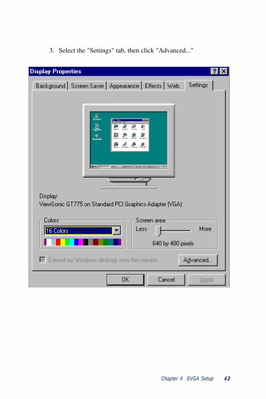
3. Select the "Settings" tab, then click "Advanced..."

44 PCA-6740 User's Manual
4. Click the "Adapter" tab, and then the "Change ..." button.

Chapter 4 SVGA Setup 45
5. Select "Display a list of all the drivers in a specific location..."then click "Next."
46 PCA-6740 User's Manual
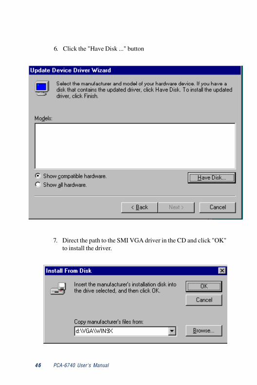
6. Click the "Have Disk ..." button
7. Direct the path to the SMI VGA driver in the CD and click "OK"to install the driver.

Chapter 4 SVGA Setup 47
8. Reboot the system.
48 PCA-6740 User's Manual
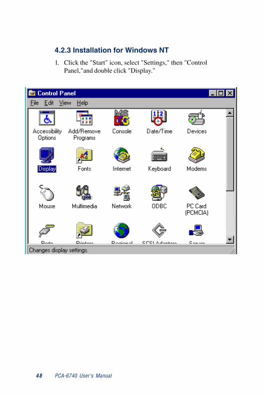
4.2.3 Installation for Windows NT
1. Click the "Start" icon, select "Settings," then "ControlPanel,"and double click "Display."
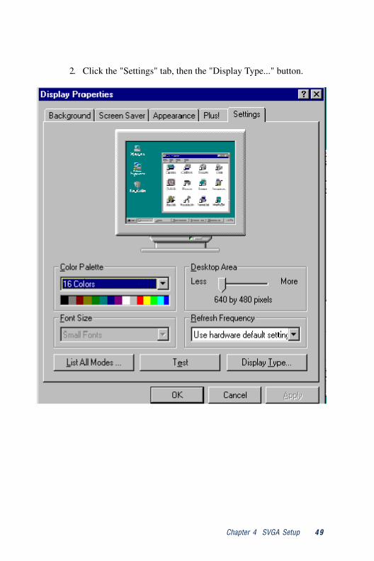
Chapter 4 SVGA Setup 49
2. Click the "Settings" tab, then the "Display Type..." button.
50 PCA-6740 User's Manual
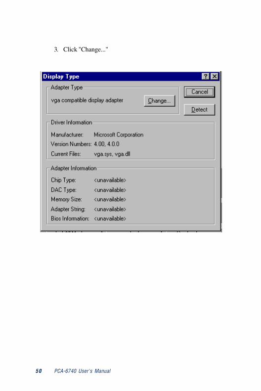
3. Click "Change..."
Chapter 4 SVGA Setup 51
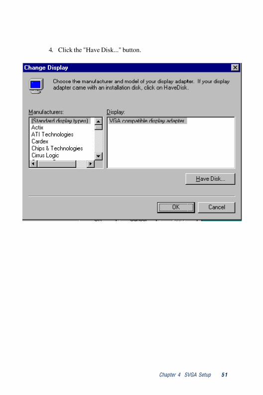
4. Click the "Have Disk..." button.
52 PCA-6740 User's Manual
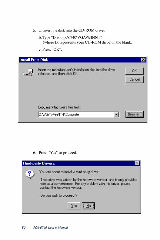
5. a. Insert the disk into the CD-ROM drive.
b. Type “D:\slotpc\6740\VGA\WINNT” (where D: represents your CD-ROM drive) in the blank.
c. Press “OK”.
6. Press "Yes" to proceed.
Chapter 4 SVGA Setup 53
4.3 Further informationFor further information about the PCI/SVGA installation in yourPCA-6740, including driver updates, troubleshooting guides andFAQ lists, visit the following web resources:
SMI web site: http://www.siliconmotion.com
Advantech web sites: http://www.advantech.comhttp://www.advantech.com.tw
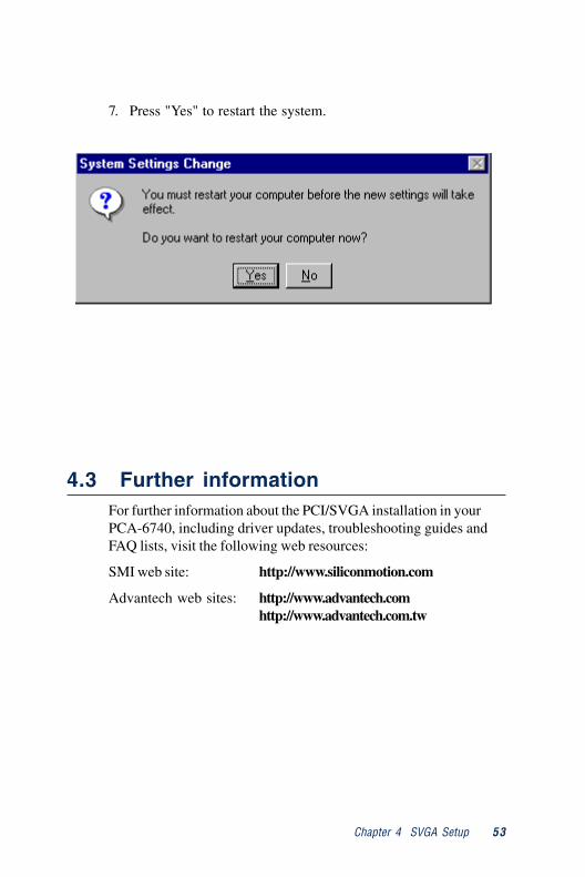
7. Press "Yes" to restart the system.

54 PCA-6740 User's Manual
PCI Bus EthernetInterfaceThis chapter provides information onEthernet configuration.
• Introduction
• Installation of Ethernet driver forWindows 95/98/NT
• Further informationC
HA
PT
ER
5
56 PCA-6740 User's Manual
5.1 IntroductionThe PCA-6740 is equipped with a high performance 32-bit Ethernetchipset which is fully compliant with IEEE 802.3 100 Mbps CSMA/CD standards. It is supported by major network operating systems.It is also both 100Base-T and 10Base-T compatible. The mediumtype can be configured via the RSET8139.exe program included onthe utility disk.
The Ethernet port provides a standard RJ-45 jack on board. Thenetwork boot feature can be utilized by incorporating the bootROM image files for the appropriate network operating system. Theboot ROM BIOS files are combined with system BIOS, which canbe enabled/disabled in the BIOS setup.
5.2 Installation of Ethernet driverBefore installing the Ethernet driver, note the procedures below.You must know which operating system you are using in yourPCA-6740, and then refer to the corresponding installation flowchart. Then just follow the steps described in the flow chart. Youwill quickly and successfully complete the installation, even if youare not familiar with instructions for MS-DOS or Windows.
Note: The Windows illustrations in this chapter areexamples only. You must pay attention to andfollow the instructions which appear on yourscreen.
Chapter 5 PCI Bus Ethernet Interface 57
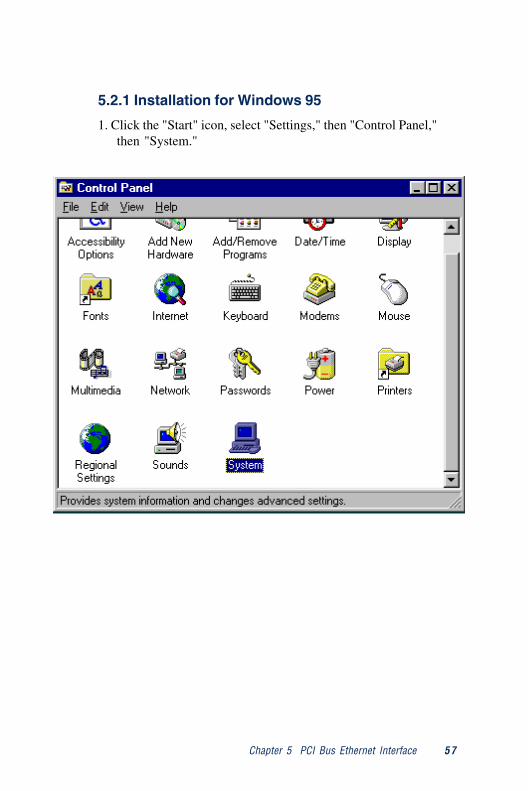
5.2.1 Installation for Windows 95
1. Click the "Start" icon, select "Settings," then "Control Panel,"then "System."
58 PCA-6740 User's Manual
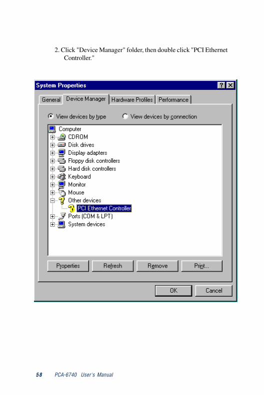
2. Click "Device Manager" folder, then double click "PCI EthernetController."
Chapter 5 PCI Bus Ethernet Interface 59
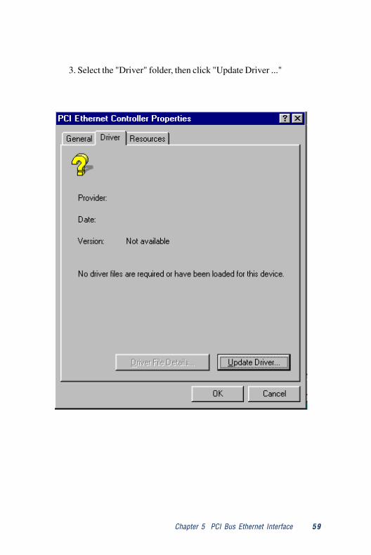
3. Select the "Driver" folder, then click "Update Driver ..."
60 PCA-6740 User's Manual
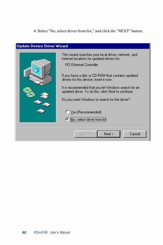
4. Select "No, select driver from list," and click the "NEXT" button.
Chapter 5 PCI Bus Ethernet Interface 61
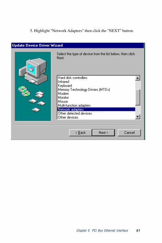
5. Highlight "Network Adapters" then click the "NEXT" button.
62 PCA-6740 User's Manual
6. Click "Have Disk ..." to update the LAN driver.
7. Direct the path to the LAN driver to install it.
Chapter 5 PCI Bus Ethernet Interface 63
8. Insert "Windows 95 CD" and click "OK."
9. Reboot the system.

64 PCA-6740 User's Manual
5.2.2 Installation for Windows 98
1. Click "Start," then "Settings," and "Control Panel." Double clickon the "System" icon.
Chapter 5 PCI Bus Ethernet Interface 65
2. Click the "Device Manager" tab, then highlight "PCI EthernetController"
66 PCA-6740 User's Manual
3. Click on "Properties," select the "Driver" tab, then "UpdateDriver..."
Chapter 5 PCI Bus Ethernet Interface 67
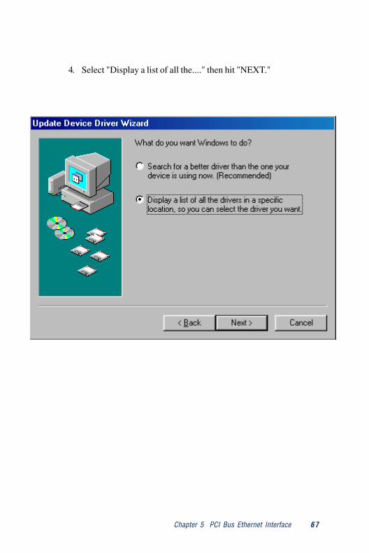
4. Select "Display a list of all the...." then hit "NEXT."
68 PCA-6740 User's Manual
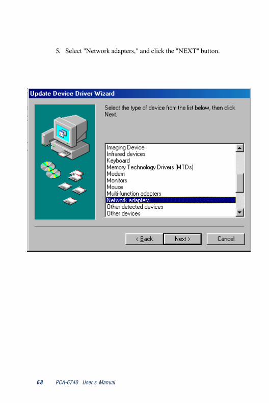
5. Select "Network adapters," and click the "NEXT" button.
Chapter 5 PCI Bus Ethernet Interface 69
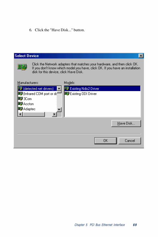
6. Click the "Have Disk..." button.
70 PCA-6740 User's Manual
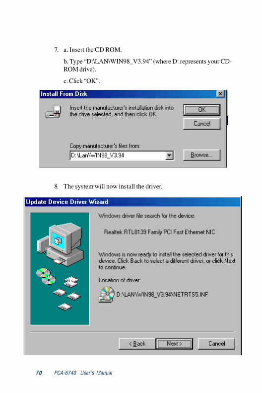
7. a. Insert the CD ROM.
b. Type “D:\LAN\WIN98_V3.94” (where D: represents your CD-ROM drive).
c. Click “OK”.
8. The system will now install the driver.
Chapter 5 PCI Bus Ethernet Interface 71
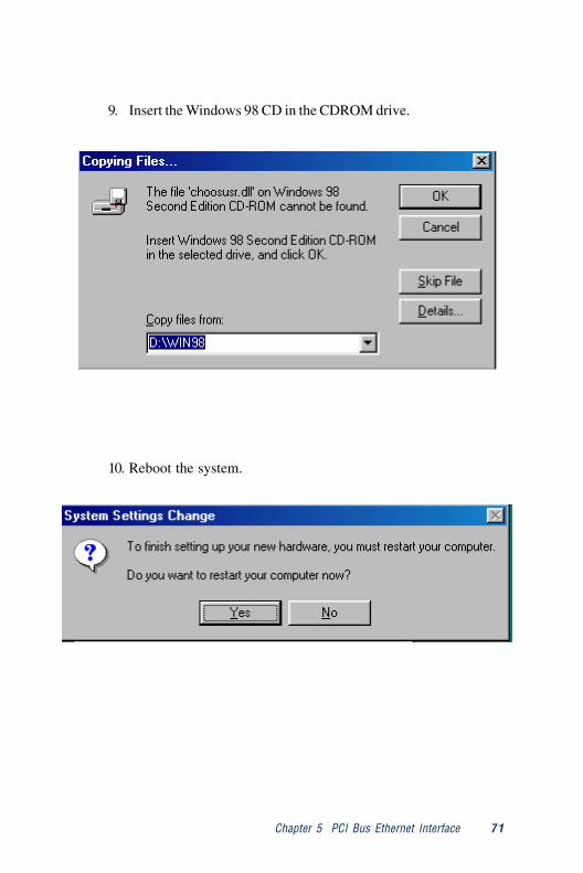
9. Insert the Windows 98 CD in the CDROM drive.
10. Reboot the system.
72 PCA-6740 User's Manual
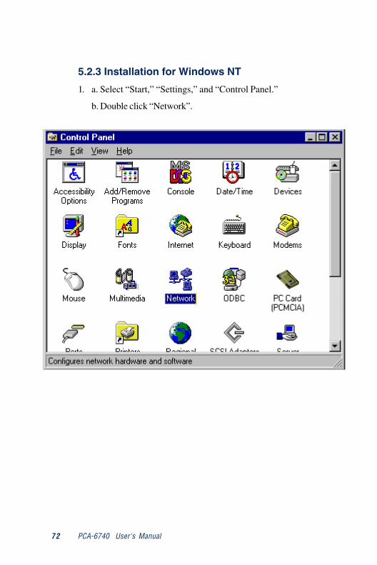
5.2.3 Installation for Windows NT
1. a. Select “Start,” “Settings,” and “Control Panel.”
b. Double click “Network”.
Chapter 5 PCI Bus Ethernet Interface 73
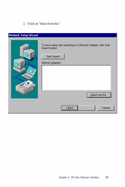
2. Click on "Select from list."
74 PCA-6740 User's Manual
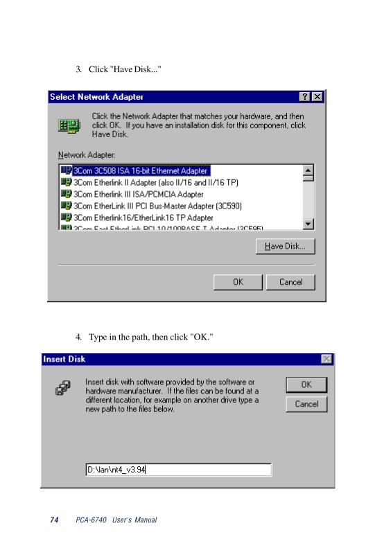
3. Click "Have Disk..."
4. Type in the path, then click "OK."
Chapter 5 PCI Bus Ethernet Interface 75
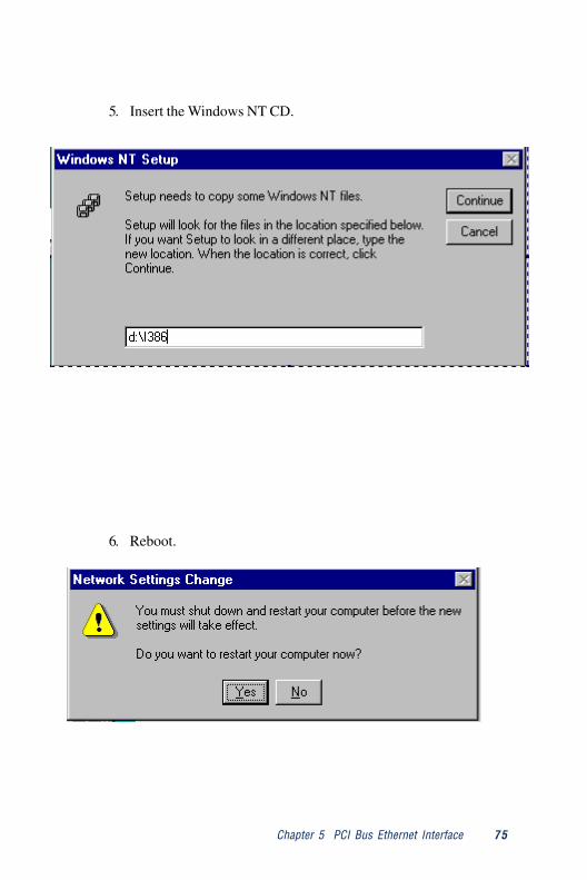
5. Insert the Windows NT CD.
6. Reboot.

76 PCA-6740 User's Manual
5.3 Further informationRealtek website: www.realtek.com
Advantech websites:www.advantech.comwww.advantech.com.tw
Floppy Disk DriveInstallationThis chapter provides information oninstallation of a standard floppy drive forWindows 95 and 98.
CH
AP
TE
R
6
78 PCA-6740 User's Manual
6.1 Installation for Windows 951. After BIOS POST, press “Shift+F5” to interrupt the system.
2. Execute the utility file, STM95fdc.bat, which is on the accompa-nying CD. This will create directory C:\STM95FDC on the Cdrive and copy files into it.
3. Reboot the system and restart Windows 95.
4. Click the “Start” button, select “Settings,” then “ControlPanel,” and double click the “System” icon.
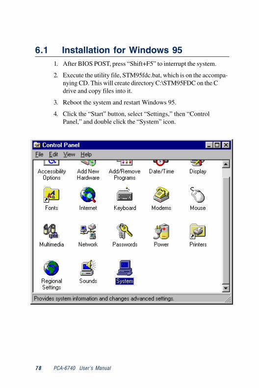
Chapter 6 Floppy Disk Drive Installation79
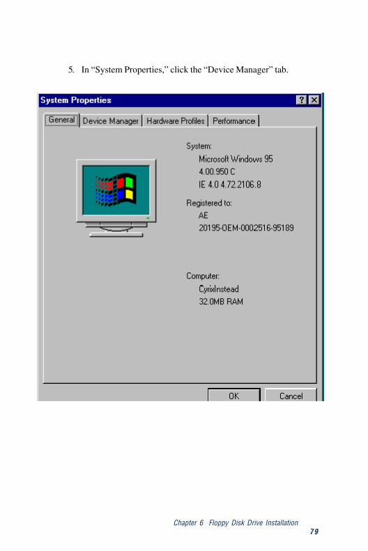
5. In “System Properties,” click the “Device Manager” tab.
80 PCA-6740 User's Manual
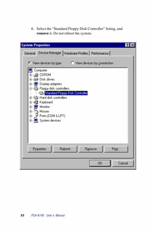
6. Select the “Standard Floppy Disk Controller” listing, andremove it. Do not reboot the system.
Chapter 6 Floppy Disk Drive Installation81
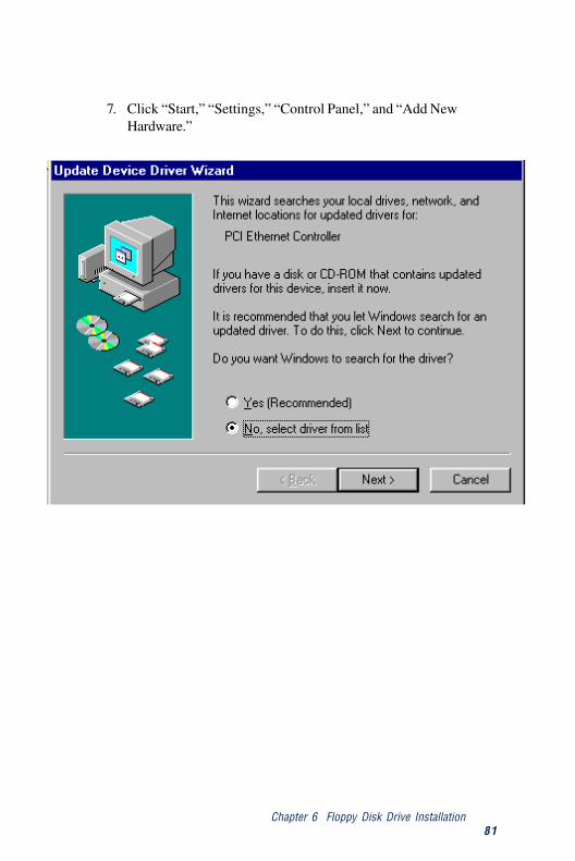
7. Click “Start,” “Settings,” “Control Panel,” and “Add NewHardware.”
82 PCA-6740 User's Manual
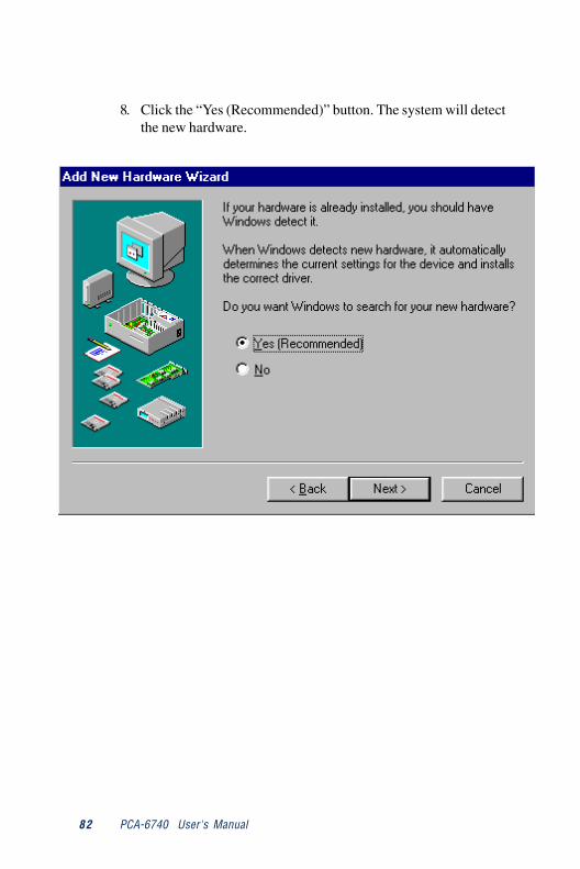
8. Click the “Yes (Recommended)” button. The system will detectthe new hardware.
Chapter 6 Floppy Disk Drive Installation83
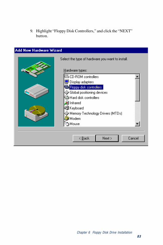
9. Highlight “Floppy Disk Controllers,” and click the “NEXT”button.
84 PCA-6740 User's Manual
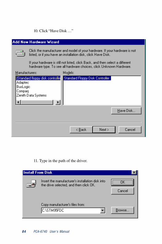
10. Click “Have Disk …”
11. Type in the path of the driver.
Chapter 6 Floppy Disk Drive Installation85
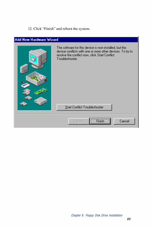
12. Click “Finish” and reboot the system.
86 PCA-6740 User's Manual
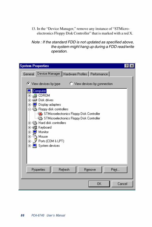
13. In the “Device Manager,” remove any instance of “STMicro-electronics Floppy Disk Controller” that is marked with a red X.
Note : If the standard FDD is not updated as specified above,the system might hang up during a FDD read/writeoperation.
Chapter 6 Floppy Disk Drive Installation87
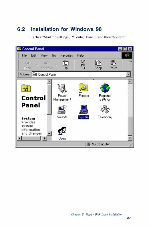
6.2 Installation for Windows 981. Click “Start,” “Settings,” “Control Panel,” and then “System”
88 PCA-6740 User's Manual
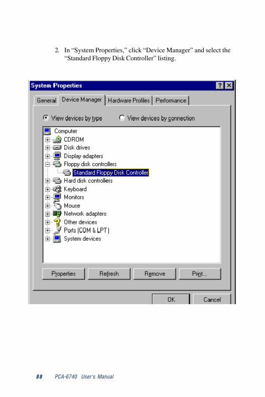
2. In “System Properties,” click “Device Manager” and select the“Standard Floppy Disk Controller” listing.
Chapter 6 Floppy Disk Drive Installation89
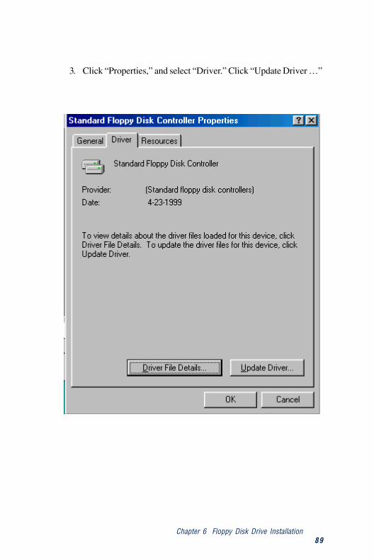
3. Click “Properties,” and select “Driver.” Click “Update Driver …”
90 PCA-6740 User's Manual
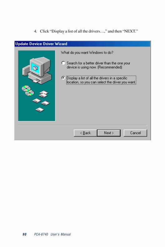
4. Click “Display a list of all the drivers…,” and then “NEXT.”
Chapter 6 Floppy Disk Drive Installation91
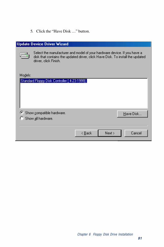
5. Click the “Have Disk …” button.
92 PCA-6740 User's Manual
6. Type in the path of the STM floppy controller, then hit "OK."
7. Reboot the system.
This appendix contains information of adetailed or specialized nature. It includes:
• IDE hard drive connector
• Floppy drive connector
• Parallel port connector
• LCD connector
• External speaker connector
• Keyboard lock connector
• System reset switch connector
• IR connector
• HDD LED connector
• ATX power button connector
• ATX power standby connector
• COM2 RS-232/422/485 serial port connector
• CRT display connector
• COM2 RS-232 connector
• COM1 RS-232 connector
• Internal keyboard connector
• AT power connector
• Keyboard and mouse connector
AP
PE
ND
IX
APin Assignments
9 4 PCA-6740 User's Manual
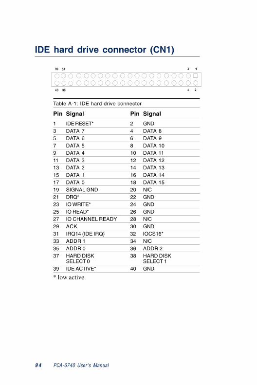
IDE hard drive connector (CN1)
Table A-1: IDE hard drive connector
Pin Signal Pin Signal
1 IDE RESET* 2 GND3 DATA 7 4 DATA 85 DATA 6 6 DATA 97 DATA 5 8 DATA 109 DATA 4 10 DATA 1111 DATA 3 12 DATA 1213 DATA 2 14 DATA 1315 DATA 1 16 DATA 1417 DATA 0 18 DATA 1519 SIGNAL GND 20 N/C21 DRQ* 22 GND23 IO WRITE* 24 GND25 IO READ* 26 GND27 IO CHANNEL READY 28 N/C29 ACK 30 GND31 IRQ14 (IDE IRQ) 32 IOCS16*33 ADDR 1 34 N/C35 ADDR 0 36 ADDR 237 HARD DISK 38 HARD DISK
SELECT 0 SELECT 139 IDE ACTIVE* 40 GND
* low active
Appendix A Pin Assignments 9 5
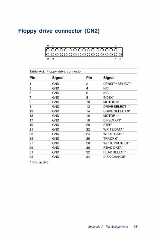
Floppy drive connector (CN2)
Table A-2: Floppy drive connector
Pin Signal Pin Signal
1 GND 2 DENSITY SELECT*3 GND 4 N/C5 GND 6 N/C7 GND 8 INDEX*9 GND 10 MOTOR 0*11 GND 12 DRIVE SELECT 1*13 GND 14 DRIVE SELECT 0*15 GND 16 MOTOR 1*17 GND 18 DIRECTION*19 GND 20 STEP*21 GND 22 WRITE DATA*23 GND 24 WRITE GATE*25 GND 26 TRACK 0*27 GND 28 WRITE PROTECT*29 GND 30 READ DATA*31 GND 32 HEAD SELECT*33 GND 34 DISK CHANGE*
* low active
434
33 3
32
31 1
2
9 6 PCA-6740 User's Manual
Parallel port connector (CN3)
Table A-3: Parallel port connector
Pin Signal
1 STROBE*2 AUTOFD*3 D04 ERROR*5 D16 INIT*7 D28 SLCTINI*9 D310 GND11 D412 GND13 D514 GND15 D616 GND17 D718 GND19 ACK*20 GND21 BUSY22 GND23 PE24 GND25 SLCT26 GND
426
25 3
24
23 1
2
* low active
Appendix A Pin Assignments 9 7
Flat panel display connector (CN4)
Table A-4: Flat panel display connector
Pin Function Pin Function
1 +12 V 2 +12 V3 GND 4 GND5 VDD 6 VDD7 ENAVEE 8 GND9 P0 10 P111 P2 12 P313 P4 14 P515 P6 16 P717 P8 18 P919 P10 20 P1121 P12 22 P1323 P14 24 P1525 P16 26 P1727 P18 28 P1929 P20 30 P2131 P22 32 P2333 GND 34 GND35 SFK 36 FLM37 DE (M) 38 LP39 GND 40 ENABKL41 N/C 42 N/C43 VSAFE (ENAVDD) 44 N/C
9 8 PCA-6740 User's Manual
CN6- External speaker (pins 1,3,5,7)
External speakerconnector
Table A-5a: External speaker connector
Pin Signal
1 + 5 V3 N/C5 Internal speaker input7 External speaker signal
CN6- Keyboard lock connector (pins 2,4)
Keyboard LockConnector
Table A-5b: Keyboard lock connector
Pin Signal
2 keyboard lock4 GND
Appendix A Pin Assignments 9 9
CN6- System reset switch conn (pins 9,11)
Reset Connector
Table A-5c: System reset switch connector
Pin Signal
9 MR_RESET11 GND
CN6- IR connector (pins 12,14,16,18,20)
Table A-5d: IR connector
Pin Signal
12 +5 V14 N/C16 IR_RX18 GND20 IR_TX
IR connector
100 PCA-6740 User's Manual
CN6- ATX power button (pins 17,19)
Table A-5f: ATX power button
Pin Signal
17 Power ON19 GND
ATX powerbutton connector
CN6- HDD LED connector (pins 13,15)
HDD LED Connector
Table A-5e: HDD LED connector
Pin Signal
13 IDE LED +15 IDE LED -

Appendix A Pin Assignments 101
LCD Inverter Power (CN8)
Table A-7: LCD Inverter connector
Pin Signal
1 12V2 GND3 Backlight On/Off Control4 Backlight Control5 5V
5
4
2
3
1
ATX power standby connector (CN7)
Table A-6: ATX power standby connector
Pin Signal
1 5 V SB2 N/C3 PS_ON
1
2
3
102 PCA-6740 User's Manual
857
6
9
324
1
10
COM2 RS-422/485 connector (CN13)
Table A-9: COM2 RS-232/422/485 connector
Pin RS-422 port RS-485 port
1 TXD- DATA-2 N/C N/C3 TXD+ DATA+4 N/C N/C5 RXD+ N/C6 N/C N/C7 RXD- N/C8 N/C N/C9 GND GND10 N/C N/C
CRT Display Connector (CN9)
Table A-8: CRT display connector
Pin Signal Pin Signal
1 RED 9 N/C2 GREEN 10 GND3 BLUE 11 N/C4 N/C 12 N/C5 GND 13 H-SYNC6 GND 14 V-SYNC7 GND 15 N/C8 GND
610
15
16
11
5
Appendix A Pin Assignments 103
COM1 RS-232 connector (CN15)
Table A-11: COM1 RS-232 connector
Pin Signal
1 DCD2 RXD3 TXD4 DTR5 GND6 DSR7 RTS8 CTS9 RI
1 5
96
32 4
7 8
857
6
9
324
1
10
COM2 RS-232 connector (CN14)
Table A-10: COM2 RS-232 connector
Pin RS-232 port Pin RS-232 port
1 DCD 6 CTS2 DSR 7 DTR3 RxD 8 RI4 RTS 9 GND5 TxD 10 N/C
104 PCA-6740 User's Manual
AT power connector (CN17)
Table A-13: AT power connector
Pin Signal
1 +12 V2 GND3 GND4 +5 V
1
2
4
3
Internal keyboard connector (CN16)
Table A-12: External keyboard connector
Pin Signal
1 CLK2 DATA3 NC4 GND5 + 5 V
5
4
2
3
1
Appendix A Pin Assignments 105
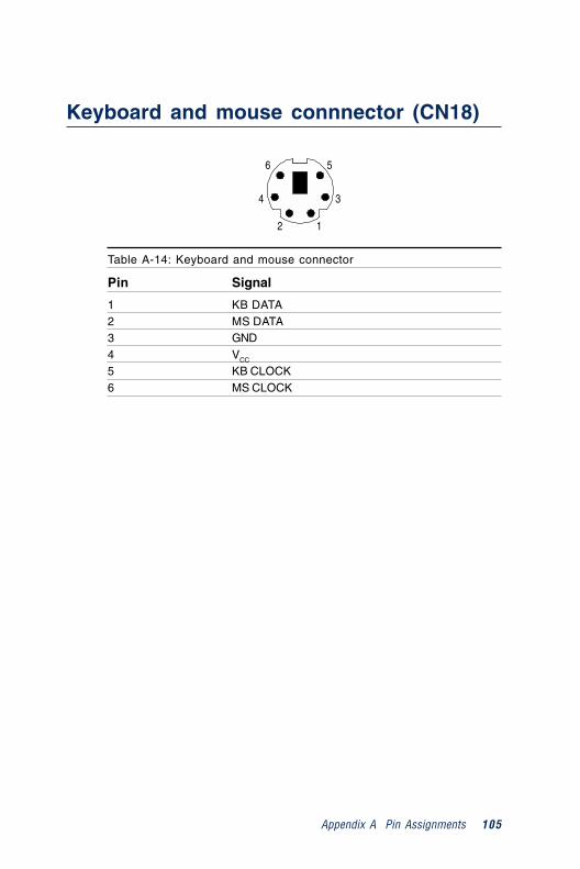
Keyboard and mouse connnector (CN18)
Table A-14: Keyboard and mouse connector
Pin Signal
1 KB DATA2 MS DATA3 GND4 VCC
5 KB CLOCK6 MS CLOCK
5
3
12
4
6

106 PCA-6740 User's Manual
SystemAssignments• System I/O ports
• DMA channel assignments
• Interrupt assignments
• 1st MB memory map
AP
PE
ND
IX
B
108 PCA-6740F User's Manual
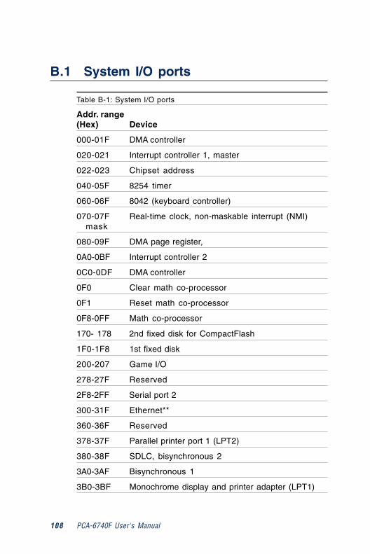
B.1 System I/O ports
Table B-1: System I/O ports
Addr. range(Hex) Device
000-01F DMA controller
020-021 Interrupt controller 1, master
022-023 Chipset address
040-05F 8254 timer
060-06F 8042 (keyboard controller)
070-07F Real-time clock, non-maskable interrupt (NMI)mask
080-09F DMA page register,
0A0-0BF Interrupt controller 2
0C0-0DF DMA controller
0F0 Clear math co-processor
0F1 Reset math co-processor
0F8-0FF Math co-processor
170- 178 2nd fixed disk for CompactFlash
1F0-1F8 1st fixed disk
200-207 Game I/O
278-27F Reserved
2F8-2FF Serial port 2
300-31F Ethernet**
360-36F Reserved
378-37F Parallel printer port 1 (LPT2)
380-38F SDLC, bisynchronous 2
3A0-3AF Bisynchronous 1
3B0-3BF Monochrome display and printer adapter (LPT1)
Appendix B System Assignments 109
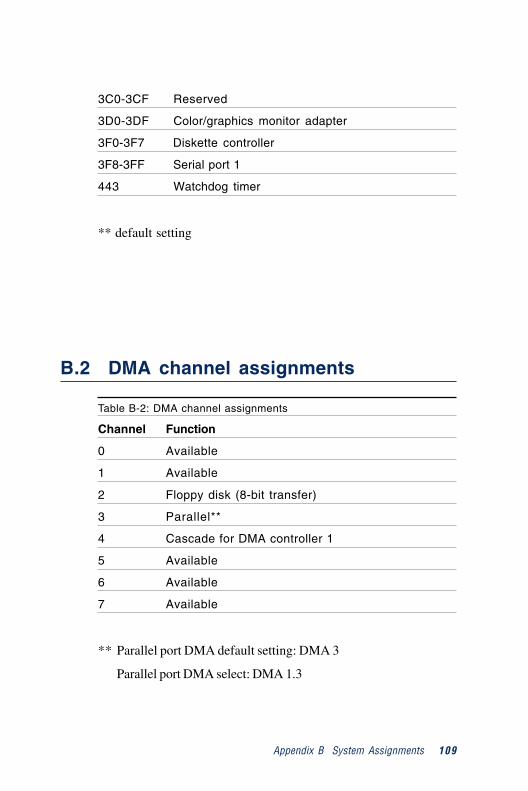
B.2 DMA channel assignments
Table B-2: DMA channel assignments
Channel Function
0 Available
1 Available
2 Floppy disk (8-bit transfer)
3 Parallel**
4 Cascade for DMA controller 1
5 Available
6 Available
7 Available
** Parallel port DMA default setting: DMA 3
Parallel port DMA select: DMA 1.3
3C0-3CF Reserved
3D0-3DF Color/graphics monitor adapter
3F0-3F7 Diskette controller
3F8-3FF Serial port 1
443 Watchdog timer
** default setting
110 PCA-6740F User's Manual
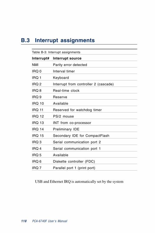
B.3 Interrupt assignments
Table B-3: Interrupt assignments
Interrupt# Interrupt source
NMI Parity error detected
IRQ 0 Interval timer
IRQ 1 Keyboard
IRQ 2 Interrupt from controller 2 (cascade)
IRQ 8 Real-time clock
IRQ 9 Reserve
IRQ 10 Available
IRQ 11 Reserved for watchdog timer
IRQ 12 PS/2 mouse
IRQ 13 INT from co-processor
IRQ 14 Preliminary IDE
IRQ 15 Secondary IDE for CompactFlash
IRQ 3 Serial communication port 2
IRQ 4 Serial communication port 1
IRQ 5 Available
IRQ 6 Diskette controller (FDC)
IRQ 7 Parallel port 1 (print port)
USB and Ethernet IRQ is automatically set by the system
Appendix B System Assignments 111
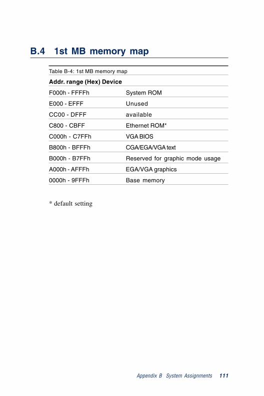
B.4 1st MB memory map
Table B-4: 1st MB memory map
Addr. range (Hex) Device
F000h - FFFFh System ROM
E000 - EFFF Unused
CC00 - DFFF available
C800 - CBFF Ethernet ROM*
C000h - C7FFh VGA BIOS
B800h - BFFFh CGA/EGA/VGA text
B000h - B7FFh Reserved for graphic mode usage
A000h - AFFFh EGA/VGA graphics
0000h - 9FFFh Base memory
* default setting

112 PCA-6740F User's Manual
AP
PE
ND
IX
CLCD ServicesThis appendix contains information of adetailed or specialized nature. It includesinformation about 18-bit TFT LCDinterfaces.

114 PCA-6740 User's Manual
C.1 LCD servicesLCD screens are very popular on Advantech's CPU cards, biscuitPCs and POS series products, such as the PCA-6135/6145/6153,and PCA-6751/PCA-6751V. "Lighting" LCDs is virtually impossiblewithout technical expertise. Advantech provides LCD lighting andintegration services to assist our customers in setting up theirsystems. Advantech's LCD lighting guide explains how to makeconnections between LCD interfaces and LCD panels, as well ashow to control contrast, brightness, V
EE source, LCD inverter and
all other factors that affect the successful installation of LCDpanels.
The following information details our LCD lighting services:
a) This policy is only valid for Advantech products that includeLCD support
b) The customer should send the following LCD components forservice:
• DC-AC inverter and cable (i.e. connector with/withoutwires) and data sheet
• LCD flat panel and cable (connector with/without wires)and complete data sheet
c) Advantech will normally charge the customer a deposit. Thedeposit will be refunded when servicing exceeds a minimumvolume
d) The customer must sign the agreement and fax it to us prior tosending the LCD package. Advantech reserves the right torefuse service if the customer cannot provide the requireddocuments and auxiliary parts
e) Advantech will supply a BIOS file and connection cable to thecustomer upon completing the service
f) A minimum of seven working days is required for completion ofservice, starting from receipt of the LCD package by Advantech
For the 18-bit TFT display support list, please contact our customerservice department for more detailed information and service files.See our web site at: http://www.advantech.com/support
Installing PC/104ModulesThis appendix gives instructions forinstalling PC/104 modules.
AP
PE
ND
IX
D
116 PCA-6740 User's Manual
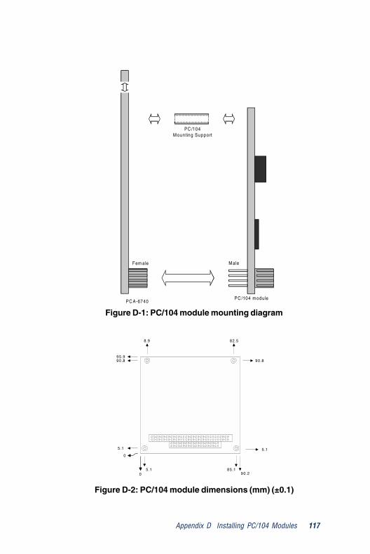
D.1 Installing PC/104 modulesThe PCA-6740F PC/104 connectors give you the flexibility to attachPC/104 modules.
Installing these modules on the PCA-6740F is quick and simple. Thefollowing steps show how to mount the PC/104 modules:
1. Remove the PCA-6740F from your system, paying particularattention to the safety instructions already mentioned above.
2. Make any jumper or link changes required to the CPU card now.Once the PC/104 module is mounted you may have difficulty inaccessing these.
3. Normal PC/104 modules have male connectors and mountdirectly onto the main card. (Refer to the diagram on thefollowing page.)
4. Mount the PC/104 module onto the CPU card by pressing themodule firmly but carefully onto the mounting connectors.
5. Secure the PC/104 module onto the CPU card using the fourmounting spacers and screws.
Appendix D Installing PC/104 Modules 117
Figure D-1: PC/104 module mounting diagram
Figure D-2: PC/104 module dimensions (mm) (±0.1)
8.9
95.990.8
5 .1
0
05.1
90.285.1
5 .1
90.8
82.5
PC A-6740
Fem ale
PC /104M ounting Support
M ale
PC /104 m odule
118 PCA-6740 User's Manual
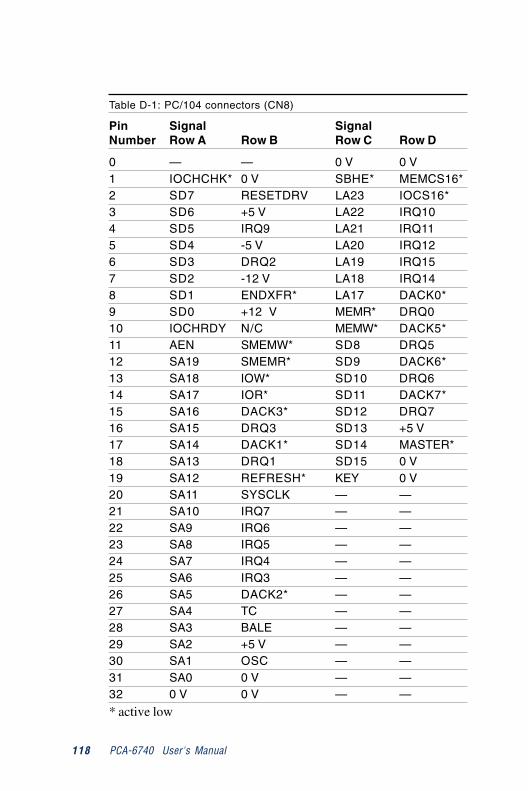
Table D-1: PC/104 connectors (CN8)
Pin Signal SignalNumber Row A Row B Row C Row D
0 — — 0 V 0 V1 IOCHCHK* 0 V SBHE* MEMCS16*2 SD7 RESETDRV LA23 IOCS16*3 SD6 +5 V LA22 IRQ104 SD5 IRQ9 LA21 IRQ115 SD4 -5 V LA20 IRQ126 SD3 DRQ2 LA19 IRQ157 SD2 -12 V LA18 IRQ148 SD1 ENDXFR* LA17 DACK0*9 SD0 +12 V MEMR* DRQ010 IOCHRDY N/C MEMW* DACK5*11 AEN SMEMW* SD8 DRQ512 SA19 SMEMR* SD9 DACK6*13 SA18 IOW* SD10 DRQ614 SA17 IOR* SD11 DACK7*15 SA16 DACK3* SD12 DRQ716 SA15 DRQ3 SD13 +5 V17 SA14 DACK1* SD14 MASTER*18 SA13 DRQ1 SD15 0 V19 SA12 REFRESH* KEY 0 V20 SA11 SYSCLK — —21 SA10 IRQ7 — —22 SA9 IRQ6 — —23 SA8 IRQ5 — —24 SA7 IRQ4 — —25 SA6 IRQ3 — —26 SA5 DACK2* — —27 SA4 TC — —28 SA3 BALE — —29 SA2 +5 V — —30 SA1 OSC — —31 SA0 0 V — —32 0 V 0 V — —
* active low

Programming theWatchdog TimerThe PCA-6740 is equipped with a watch-dog timer that resets the CPU or generatesan interrupt if processing comes to astandstill for any reason. This featureensures system reliability in industrialstandalone or unmanned environments.
EAP
PE
ND
IX

120 PCA-6740 User's Manual
E.1 Programming the watchdog timerTo program the watchdog timer, you must write a program which writesI/O port address 443 (hex). The output data is a value of time interval.The value range is from 01 (hex) to 3E (hex), and the related timeinterval is 1 sec. to 62 sec.
Data Time Interval
01 1 sec.
02 2 sec.
03 3 sec.
04 4 sec.
• •
• •
• •
3E 62 sec.
Appendix E Programming the Watchdog Timer 121
After data entry, your program must refresh the watchdog timer byrewriting the I/O port 443 (hex) while simultaneously setting it. Whenyou want to disable the watchdog timer, your program should read I/Oport 443 (hex).
The following example shows how you might program the watchdogtimer in BASIC:
10 REM Watchdog timer example program20 OUT &H443, data REM Start and restart thewatchdog30 GOSUB 1000 REM Your application task #1,40 OUT &H443, data REM Reset the timer50 GOSUB 2000 REM Your application task #2,60 OUT &H443, data REM Reset the timer70 X=INP (&H443) REM, Disable the watchdog timer80 END
1000 REM Subroutine #1, your application task• •• •• •1070 RETURN2000 REM Subroutine #2, your application task• •• •• •2090 RETURN

122 PCA-6740 User's Manual

MechanicalDrawing
AP
PE
ND
IX
F
124 PCA-6753 User's Manual
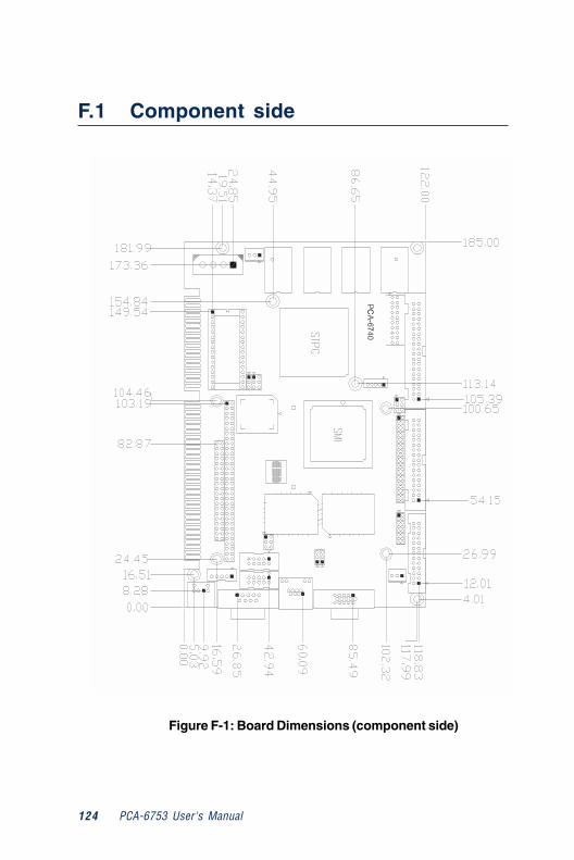
Figure F-1: Board Dimensions (component side)
F.1 Component side