Embed Size (px)
Citation preview

ISC0100
CYBERELECTRONICS
Fall 2018
The 4th lecture
Martin Jaanus NRG-308
[email protected] 56 91 31 93
Learning environment : http://isc.ttu.ee
Materials : http://isc.ttu.ee/martin

Topics
1. Diodes, transisors
2. Amplifiers, feedback
3. Operational amplifier
Devices

Semiconductors
• Low electric conductivity at room temperature
• Conductivity increases with temperature.
• Metalloids Ge, Si ,Se
• Some oxides and alloys
• Conductivity can be changed by adding doping
Silicon atoms 45,000,000
x.magnification -wikipedia

N ja P types of semiconductors
• In clean semiconductor equals number of free electrons
with number of holes. Doping greatly increases the
number of charge carriers within the crystal.
• When a doped semiconductor contains mostly free holes
it is called "p-type", and when it contains mostly free
electrons it is known as "n-type"
N type (added phosphorus) P type (added aluminium)

p-n junction
• p–n junctions are elementary "building blocks" of semiconductor electronic devices such as diodes, transistors, solar cells, LEDs, and integrated circuits
• A p–n junction is a boundary or interface between two types of semiconductor materials, p-type and n-type, inside a single crystal of semiconductor.
• The "p" (positive) side contains an excess of holes, while the "n" (negative) side contains an excess of electrons in the outer shells of the electrically neutral atoms there.
P N
P doping N doping
Free holes Free electrons

Unbiased p-n junction
• In P side is because of fewness of electrons positive charge
• In N side is because of plentyness of electrons negative
charge.
• Positive and negative charges will separate and cause
barrier voltage (in Si about 0,6...0,7 V )
Free holes Free electrons
+
++
+
++
+++
+
++
--
-- -
-- -
- --
-
--
--
P N

Reverse biased p-n junction
• Charges are pulled to edges of layers .
• Barrier layer increases.
• Electric current is missing.
Free Holes Free electrons
+
++
+
++
+
++
+
++
-
-
--
- -
-
-
-
-
-
--
- +P N
Holes
Elektrons

Forward biased p-n junction
• Barrier decreases, because charges are pulled to junction.
• From opening voltage ( ex Si 0,6...0,7 V) arises current.
Free Holes Free electrons
+
+ +
+
+
+
++
+ +
+
+
-
--
- ---
- --
-
-
-
--
+ -P N
Holes
Electrons

Nonlinear twopole
• Effect appears when materials with different properties
contacting
• Usually p- and n- type materials (silicon, germanium,
gallium arsenide) are used
• Analogue in hydraulic–
non-return valve
Anode Cathode
Electronic component - Diode

• Conductonce depends on voltage
• Main usage – to rectify AC signals
Electronic component - Diode
I is the diode current,
IS is the reverse bias saturation current
,VD is the voltage across the diode,
VT is the thermal voltage
Thermal voltage
approximately 25.85 mV at 300 K,
k is the Boltzmann constant
q is the elementary chargre
V-A characteristics

• Zener diode
• Light emitting diode , photodiode
• Tunnel diode
• Schottky diodes
Equivalent circuit of silicon diode
Electronic component - Diode
Image:wikipedia

Light emitting diode (LED)
Calculation of resistor
We use
• Kirchhoff s voltage law ,calculate VR=Vs-VL
• Ohm’s law R=VR/I
+
–Vs
Infrared - 1.1 V
Red – 2 V
Yellow – 2.2 V
Green – 2.3V
Blue - 3.3 VWhite - 3.3 V
Depends on material
„bandcap-0.4 V „ rule.
VL
The average current in normal state 10-20 mA
At 10 mA current

• It is electrically adjustable resistor(transformer of resistor)
• Hydraulic analog– valve
• With little amount of energy the large energy flow can controlled
• Threepole
• Bipolar transistor
• Field effect transistor
Electronic component - Transistor

Field effect transistor• Electric charge controls charge flow
• Voltage controlled resistor
• The most common part in microelectronics(IT)
• 50 million devices in year per person (USA 2001)
• Two channel types N or P
• Types MOSFET and J-FET
• https://www.youtube.com/watch?v=SjeK1nkiFvI
gate
source drain
Image:Blog.novaelectronica.com

Field effect transistor
http://www.electronics-tutorials.ws

Field effect transistor application
• Mosfet as an amplifier
• http://www.electronics-tutorials.ws/amplifier/mosfet-amplifier.html

• MOSFET as switch (ex. for Arduino users)
• http://www.electronics-tutorials.ws/transistor/tran_7.html
Field effect transistor application
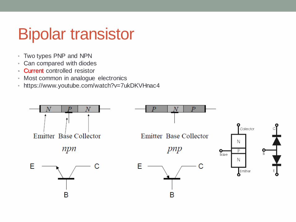
Bipolar transistor• Two types PNP and NPN
• Can compared with diodes
• Current controlled resistor
• Most common in analogue electronics
• https://www.youtube.com/watch?v=7ukDKVHnac4

Bipolar transistor application
A Bipolar NPN Transistor Configuration
rrow defines the emitter and conventional current flow,
“out” for a Bipolar NPN Transistor.)

CE
CK
CB
Bipolar transistor application• Single Stage Common Emitter Amplifier Circuit

• Transistor as a switch
Bipolar transistor application

An amplifier is an electronic device that can increase the power of a signal
using power from supply.
K
+
–Vcc
Output (V,I)Input (V,I)
• Voltage amplifier
• Current amplifier
• V-I trancducer (transfer - conductivity)
• I-V trancducer (transfer -resistance)
Transfer (amplification)
𝐾𝑉 =𝑉𝑜𝑢𝑡𝑉𝑖𝑛
, 𝐾𝑉 dB = 𝟐𝟎 ∗ log(𝐾𝑉)
𝐾𝐼 =𝐼𝑜𝑢𝑡𝐼𝑖𝑛
, 𝐾𝐼 dB = 𝟐𝟎 ∗ log(𝐾𝐼)
𝐾𝑉 usually not = 𝐾𝐼
Power amplification
𝐾𝑃 =𝑃𝑜𝑢𝑡𝑃𝑖𝑛
, 𝐾𝑃 dB = 10 ∗ log(𝐾𝑃)
Power is proportioonal with root of voltage (or current).
Amplifier

Amplifies only difference of input signal.
K
Output (V,I)
Vin1
• K is very high(until 100 000)
• Instrumental amplifiers K selecable
• The most univesal device in electronics
• If negative feedback is used (V or I),output takes state that Vin1=Vin2 .
Output Voltage𝑉𝑜𝑢𝑡=𝐾 ∗ (𝑉𝑖n1 − Vin2)
Vin2
+
-
Operational amplifier
Usually opamps have voltage inputs (input resistance is very high).
Also there are opamps with current inputs (and differential outputs). Rarely used.

By Daniel Braun - redrawn png file (from User:Omegatron),Page# 4 of datasheet,
CC BY 2.5, https://commons.wikimedia.org/w/index.php?curid=2205381

The feedback is system’s output effect to it’s input.
• Negative feedback occurs when output of a system, process, or mechanism is
fed back in a manner that tends to reduce the fluctuations in the output,
whether caused by changes in the input or by other disturbances.
(stability,taxes , adjusting euribor )
• Positive feedback is a process that occurs in a feedback loop in which the effects
of a small disturbance on a system include an increase in the magnitude
of the perturbation.(unstability, generators, explosives, economics with credit).
Feedback
By Andy Docker from England - StampedeBy Lee Jordan - Flickr, CC BY-SA 2.0,

Example: steam engine
Mechanical feedback
Rotation speed stabilizer.
Negative feedback
Images:wikipedia

𝑋𝑜𝑋𝑖
= 𝐾𝑓 =𝐾
1 + 𝐾βIf Kβ >>1 then 𝐾𝑓 =
1
β
K
Xo
Xi +-
β
Feedback circuit
Forward circuit
The base of automation!
In forward circuit can be used cheap,
unpercise components.
Feedback circuit must be percise !
(Negative )Feedback

Non inverting amplifier
K
Vout
Vin1
Output voltage𝑉𝑜𝑢𝑡=𝐾 ∗ (𝑉𝑖n1 − Vin2)
Inverted inpud is connected
To output ,using voltage divider
𝑉𝑖𝑛2 = 𝑉𝑜𝑢𝑡 ∗𝑅1
𝑅1 + 𝑅2Putting them together.
Vin2
+
- R2
R1
𝑉𝑜𝑢𝑡= 𝐾 ∗ (𝑉𝑖𝑛1 − 𝑉𝑜𝑢𝑡 ∗𝑅1
𝑅1+𝑅2) −→
𝑉𝑜𝑢𝑡= 𝑉𝑖𝑛1 ∗𝐾
1+𝐾∗𝑅1
𝑅1+𝑅2
Feedback (voltage divider) β
Operational amplifier
If Kβ >>1 then 𝐾𝑓 =1
β=
𝑅1+𝑅2
𝑅1= 1+
𝑅2
𝑅1
Vin1=Vin2

Inverting amplifier
KVout .Iout
Vin1=0
Opamp equals difference in inputVin1=0 -> Vin2=0 𝐾 ≫ ∞Input Current𝐼𝑖𝑛=𝑉𝑖n/R1Output must compensate it 𝑉𝑜𝑢𝑡=𝑅2 ∗ −𝐼𝑖𝑛Putting them together.
𝑉𝑜𝑢𝑡 = −𝑉𝑖𝑛 ∗𝑅2𝑅1
Vin2=0
+
- R2
R1
Operational amplifier
𝐾𝑓 = −𝑅2
𝑅1
Vin, Iin

Operational amplifier
Summing inverting amplifier sums several voltages
http://www.electroniccircuitsdesign.com/au
dio-circuits/4-channel-audio-mixer-circuit-
using-lm381.html
4 channel audio mixer

Operational amplifier
The circuit shown computes the difference of two voltages,
multiplied by some gain factor.


Operational amplifier
Replacing resistors in previos circuits with other elemencs
It is possible to do everything in electronics.
• Filters
• Impedance converters
• Logaritmic or exponential amplifiers
• ........
Inductance gyrator
Integrator

Operational amplifier
If positive feedback applied.
• Generators
• Comparators
• Negative impedance converter
Output is limited by supply voltage.
Comparator
In a Schmitt trigger circuit, feedback to the
non-inverting input of an amplifier pushes
the output directly away from the applied
voltage towards the maximum or minimum
voltage the amplifier can generate.