Embed Size (px)
Citation preview
FN8977Rev.0.01
Dec 1, 2017
ISL32745E6kV VDE-Reinforced Isolated 40Mbps Full-Duplex RS-485 Transceiver
DATASHEET
The ISL32745E is a galvanically isolated, high-speed differential bus transceiver, designed for full-duplex data communication on balanced transmission lines. The device uses Giant Magnetoresistance (GMR) as its isolation technology.
The part is available in a 16 Ld SOICW package with true 8mm creepage distance.
The ISL32745E delivers a minimum differential output voltage of 2.1V across a 54Ω differential load for high noise immunity and excellent data integrity.
A unique ceramic/polymer composite barrier provides 6kV reinforced isolation and 44,000 years of barrier life.
The device is compatible with 3V and 5V input supplies, allowing a simple interface to local controllers.
Current limiting and thermal shutdown features protect against output short circuits and bus contention that may cause excessive power dissipation. Receiver inputs are a full fail-safe design, ensuring a logic high R-output if A/B are open (floating) or shorted.
Applications• Industrial robotics
• Factory automation
• Security networks
• Industrial/process control networks
• Equipment covered under IEC 61010-1 Edition 3
Features• 40Mbps data rate
• 6kVRMS isolation/1000VRMS working voltage
• 12.8kV surge immunity
• 1/5 unit load allows up to 160 devices on the bus
• 3V to 5V power supplies
• 20ns propagation delay
• 5ns pulse skew
• 50kV/µs common-mode transient immunity
• 10kV ESD protection
• Low EMC footprint
• Thermal shutdown protection
• -40°C to +85°C temperature range
• Meets or exceeds ANSI RS-485 and ISO 8482:1987(E)
• 0.3” true 8mm 16 Ld SOICW package
• UL 1577 recognized
• VDE V 0884-11 (certification pending)
Related Literature• For a full list of related documents, visit our website
• ISL32745E product page
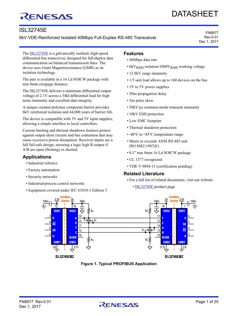
Figure 1. Typical PROFIBUS Application
ISL32745EIBZ
16
13
9,15
VDD2
B
ISODE
GND2
1
4
3
5
6
2,8
VDD1
R
DE
D
RE
GND1
Isolation Barrier 100n
5V100n
3.3V
14A
10
RB
RT
12Z
11Y
RB
ISL32745EIBZ
16
12
9,15
VDD2
Z
ISODE
GND2
1
5
6
4
3
2,8
VDD1
D
DE
R
RE
GND1
Isolation Barrier100n
5V100n
3.3V
11Y
10
RB
RT 13B
14A
RB
FN8977 Rev.0.01 Page 1 of 20Dec 1, 2017
ISL32745E 1. Overview
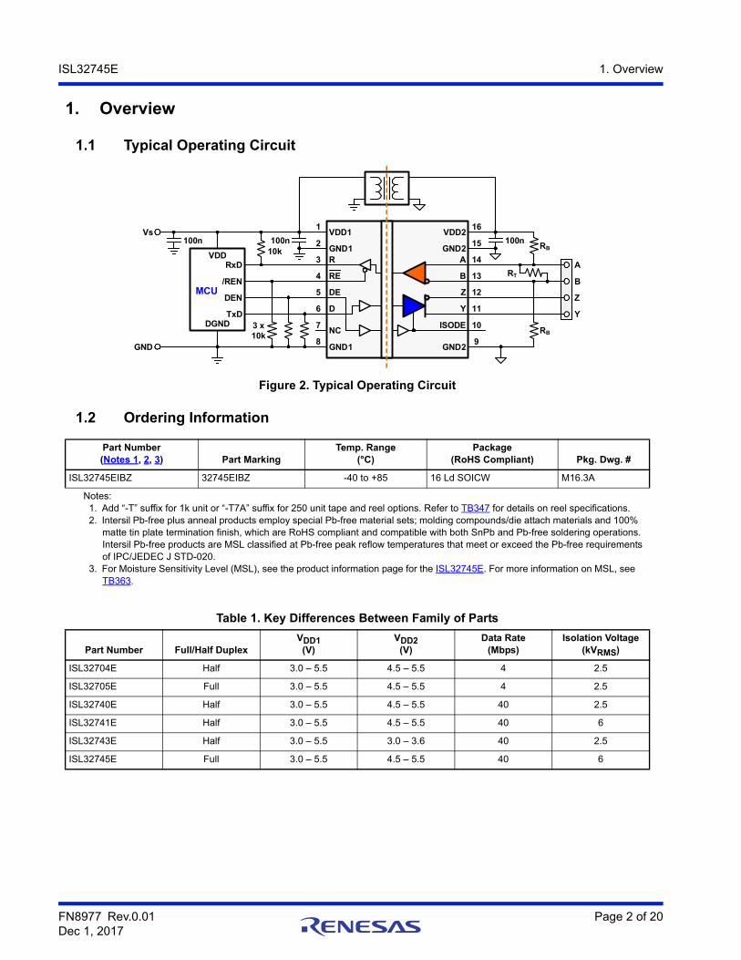
1. Overview
1.1 Typical Operating Circuit
1.2 Ordering Information
Figure 2. Typical Operating Circuit
Part Number(Notes 1, 2, 3) Part Marking
Temp. Range(°C)
Package(RoHS Compliant) Pkg. Dwg. #
ISL32745EIBZ 32745EIBZ -40 to +85 16 Ld SOICW M16.3A
Notes:1. Add “-T” suffix for 1k unit or “-T7A” suffix for 250 unit tape and reel options. Refer to TB347 for details on reel specifications.2. Intersil Pb-free plus anneal products employ special Pb-free material sets; molding compounds/die attach materials and 100%
matte tin plate termination finish, which are RoHS compliant and compatible with both SnPb and Pb-free soldering operations. Intersil Pb-free products are MSL classified at Pb-free peak reflow temperatures that meet or exceed the Pb-free requirements of IPC/JEDEC J STD-020.
3. For Moisture Sensitivity Level (MSL), see the product information page for the ISL32745E. For more information on MSL, see TB363.
Table 1. Key Differences Between Family of Parts
Part Number Full/Half DuplexVDD1
(V)VDD2
(V)Data Rate
(Mbps)Isolation Voltage
(kVRMS)
ISL32704E Half 3.0 – 5.5 4.5 – 5.5 4 2.5
ISL32705E Full 3.0 – 5.5 4.5 – 5.5 4 2.5
ISL32740E Half 3.0 – 5.5 4.5 – 5.5 40 2.5
ISL32741E Half 3.0 – 5.5 4.5 – 5.5 40 6
ISL32743E Half 3.0 – 5.5 3.0 – 3.6 40 2.5
ISL32745E Full 3.0 – 5.5 4.5 – 5.5 40 6
1
2
4
3
5
6
8
7
16
15
13
12
14
11
10
9
Y
VDD2
Z
A
B
ISODE
GND2
GND2
VDD1
R
DE
D
RE
NC
GND1
GND1100n
10k
3 x10k
100n
DGND
RxD
/REN
DEN
TxD
VDD
MCU
GND
Vs100n
RB
RT
RB
Y
Z
A
B
FN8977 Rev.0.01 Page 2 of 20Dec 1, 2017
ISL32745E 1. Overview
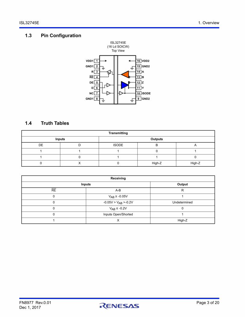
1.3 Pin Configuration
1.4 Truth Tables
ISL32745E(16 Ld SOICW)
Top View
Transmitting
Inputs Outputs
DE D ISODE B A
1 1 1 0 1
1 0 1 1 0
0 X 0 High-Z High-Z
Receiving
Inputs Output
RE A-B R
0 VAB ≥ -0.05V 1
0 -0.05V > VAB >-0.2V Undetermined
0 VAB ≤ -0.2V 0
0 Inputs Open/Shorted 1
1 X High-Z
1
2
4
3
5
6
8
7
16
15
13
12
14
11
10
9
Y
VDD2
Z
A
B
ISODE
GND2
GND2
VDD1
R
DE
D
RE
NC
GND1
GND1
FN8977 Rev.0.01 Page 3 of 20Dec 1, 2017
ISL32745E 1. Overview
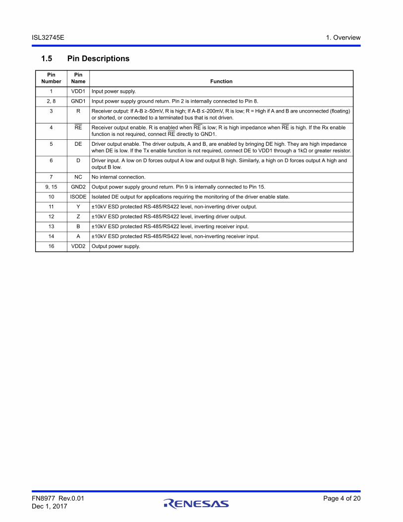
1.5 Pin Descriptions
Pin Number
Pin Name Function
1 VDD1 Input power supply.
2, 8 GND1 Input power supply ground return. Pin 2 is internally connected to Pin 8.
3 R Receiver output: If A-B ≥-50mV, R is high; If A-B ≤-200mV, R is low; R = High if A and B are unconnected (floating) or shorted, or connected to a terminated bus that is not driven.
4 RE Receiver output enable. R is enabled when RE is low; R is high impedance when RE is high. If the Rx enable function is not required, connect RE directly to GND1.
5 DE Driver output enable. The driver outputs, A and B, are enabled by bringing DE high. They are high impedance when DE is low. If the Tx enable function is not required, connect DE to VDD1 through a 1kΩ or greater resistor.
6 D Driver input. A low on D forces output A low and output B high. Similarly, a high on D forces output A high and output B low.
7 NC No internal connection.
9, 15 GND2 Output power supply ground return. Pin 9 is internally connected to Pin 15.
10 ISODE Isolated DE output for applications requiring the monitoring of the driver enable state.
11 Y ±10kV ESD protected RS-485/RS422 level, non-inverting driver output.
12 Z ±10kV ESD protected RS-485/RS422 level, inverting driver output.
13 B ±10kV ESD protected RS-485/RS422 level, inverting receiver input.
14 A ±10kV ESD protected RS-485/RS422 level, non-inverting receiver input.
16 VDD2 Output power supply.
FN8977 Rev.0.01 Page 4 of 20Dec 1, 2017
ISL32745E 2. Specifications
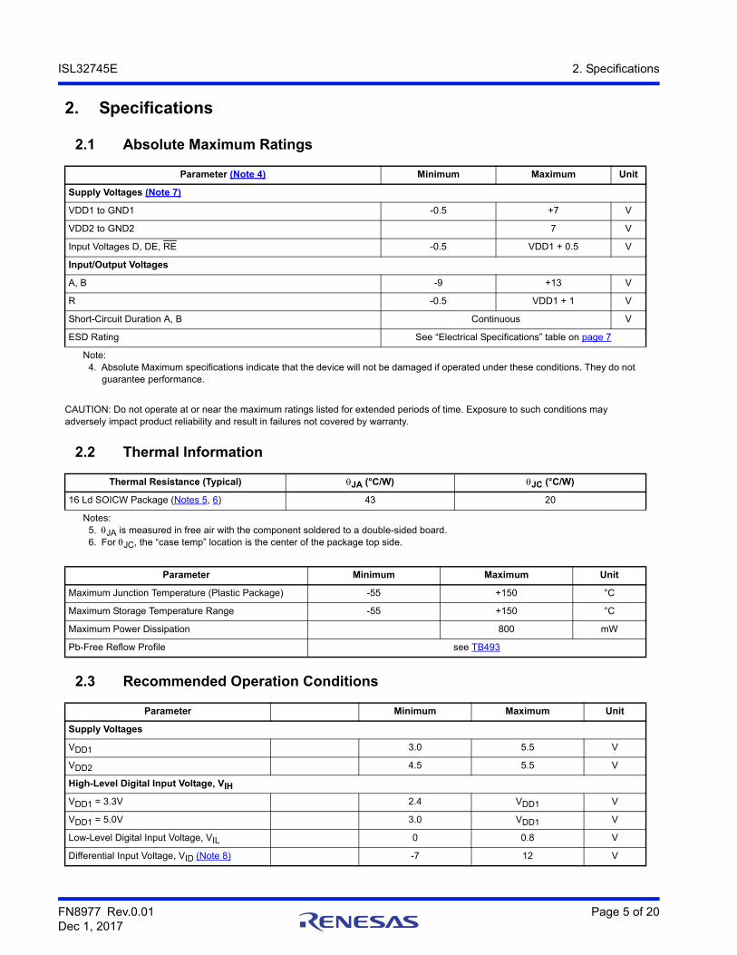
2. Specifications
2.1 Absolute Maximum Ratings
CAUTION: Do not operate at or near the maximum ratings listed for extended periods of time. Exposure to such conditions may adversely impact product reliability and result in failures not covered by warranty.
2.2 Thermal Information
2.3 Recommended Operation Conditions
Parameter (Note 4) Minimum Maximum Unit
Supply Voltages (Note 7)
VDD1 to GND1 -0.5 +7 V
VDD2 to GND2 7 V
Input Voltages D, DE, RE -0.5 VDD1 + 0.5 V
Input/Output Voltages
A, B -9 +13 V
R -0.5 VDD1 + 1 V
Short-Circuit Duration A, B Continuous V
ESD Rating See “Electrical Specifications” table on page 7
Note:4. Absolute Maximum specifications indicate that the device will not be damaged if operated under these conditions. They do not
guarantee performance.
Thermal Resistance (Typical) JA (°C/W) JC (°C/W)
16 Ld SOICW Package (Notes 5, 6) 43 20
Notes:5. JA is measured in free air with the component soldered to a double-sided board.6. For JC, the “case temp” location is the center of the package top side.
Parameter Minimum Maximum Unit
Maximum Junction Temperature (Plastic Package) -55 +150 °C
Maximum Storage Temperature Range -55 +150 °C
Maximum Power Dissipation 800 mW
Pb-Free Reflow Profile see TB493
Parameter Minimum Maximum Unit
Supply Voltages
VDD1 3.0 5.5 V
VDD2 4.5 5.5 V
High-Level Digital Input Voltage, VIH
VDD1 = 3.3V 2.4 VDD1 V
VDD1 = 5.0V 3.0 VDD1 V
Low-Level Digital Input Voltage, VIL 0 0.8 V
Differential Input Voltage, VID (Note 8) -7 12 V
FN8977 Rev.0.01 Page 5 of 20Dec 1, 2017
ISL32745E 2. Specifications
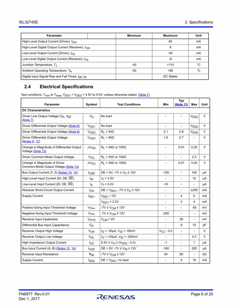
2.4 Electrical Specifications
High-Level Output Current (Driver), IOH 60 mA
High-Level Digital Output Current (Receiver), IOH 8 mA
Low-Level Output Current (Driver), IOL -60 mA
Low-Level Digital Output Current (Receiver), IOL -8 mA
Junction Temperature, TJ -40 +110 °C
Ambient Operating Temperature, TA -40 +85 °C
Digital Input Signal Rise and Fall Times, tIR, tIF DC Stable
Test conditions: Tmin to Tmax, VDD1 = VDD2 = 4.5V to 5.5V; unless otherwise stated. (Note 7)
Parameter Symbol Test Conditions MinTyp
(Note 11) Max Unit
DC Characteristics
Driver Line Output Voltage (VA, VB) (Note 7)
VO No load - - VDD2 V
Driver Differential Output Voltage (Note 8) VOD1 No load - - VDD2 V
Driver Differential Output Voltage (Note 8) VOD2 RL = 54Ω 2.1 2.8 VDD2 V
Driver Differential Output Voltage(Notes 8, 12)
VOD3 RL = 60Ω 1.9 2.7 - V
Change in Magnitude of Differential Output Voltage (Note 13)
VOD RL = 54Ω or 100Ω - 0.01 0.20 V
Driver Common-Mode Output Voltage VOC RL = 54Ω or 100Ω - - 2.5 V
Change in Magnitude of Driver Common-Mode Output Voltage (Note 13)
VOC RL = 54Ω or 100Ω - 0.01 0.20 V
Bus Output Current (Y, Z) (Notes 10, 14) IOZD DE = 0V, -7V ≤ VO ≤ 12V -100 - 100 µA
High-Level Input Current (DI, DE, RE) IIH VI = 3.5V - - 10 µA
Low-Level Input Current (DI, DE, RE) IIL VI = 0.4V -10 - - µA
Absolute Short-Circuit Output Current IOS DE = VDD1, -7V ≤ VO ≤ 12V - - ±250 mA
Supply Current IDD1 VDD1 = 5V - 4 6 mA
VDD1 = 3.3V - 3 4 mA
Positive-Going Input Threshold Voltage VTH+ -7V ≤ VCM ≤ 12V - - -50 mV
Negative-Going Input Threshold Voltage VTH- -7V ≤ VCM ≤ 12V -200 - - mV
Receiver Input Hysteresis VHYS VCM = 0V - 28 - mV
Differential Bus Input Capacitance CD - 9 12 pF
Receiver Output High Voltage VOH IO = -20µA, VID = -50mV VCC - 0.2 - - V
Receiver Output Low Voltage VOL IO = +20µA, VID = -200mV - - 0.2 V
High Impedance Output Current IOZ 0.4V ≤ VO ≤ (VDD2 - 0.5) -1 - 1 µA
Bus Input Current (A, B) (Notes 10, 14) IOZD DE = 0V, -7V ≤ VIN ≤ 12V -160 - 220 µA
Receiver Input Resistance RIN -7V ≤ VCM ≤ 12V 54 80 - kΩ
Supply Current IDD2 DE = VDD1, no load - 5 16 mA
Parameter Minimum Maximum Unit
FN8977 Rev.0.01 Page 6 of 20Dec 1, 2017
ISL32745E 2. Specifications
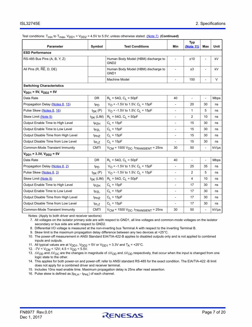
ESD Performance
RS-485 Bus Pins (A, B, Y, Z) Human Body Model (HBM) discharge to GND2
- ±10 - kV
All Pins (R, RE, D, DE) Human Body Model (HBM) discharge to GND1
- ±3 - kV
Machine Model - 150 - V
Switching Characteristics
VDD1 = 5V, VDD2 = 5V
Data Rate DR RL = 54Ω, CL = 50pF 40 - - Mbps
Propagation Delay (Notes 8, 15) tPD VO = -1.5V to 1.5V, CL = 15pF - 20 30 ns
Pulse Skew (Notes 8, 16) tSK (P) VO = -1.5V to 1.5V, CL = 15pF - 1 5 ns
Skew Limit (Note 9) tSK (LIM) RL = 54Ω, CL = 50pF - 2 10 ns
Output Enable Time to High Level tPZH CL = 15pF - 15 30 ns
Output Enable Time to Low Level tPZL CL = 15pF - 15 30 ns
Output Disable Time from High Level tPHZ CL = 15pF - 15 30 ns
Output Disable Time from Low Level tPLZ CL = 15pF - 15 30 ns
Common-Mode Transient Immunity CMTI VCM = 1500 VDC, tTRANSIENT = 25ns 30 50 - kV/µs
VDD1 = 3.3V, VDD2 = 5V
Data Rate DR RL = 54Ω, CL = 50pF 40 - - Mbps
Propagation Delay (Notes 8, 2) tPD VO = -1.5V to 1.5V, CL = 15pF - 25 35 ns
Pulse Skew (Notes 8, 3) tSK (P) VO = -1.5V to 1.5V, CL = 15pF - 2 5 ns
Skew Limit (Note 9) tSK (LIM) RL = 54Ω, CL = 50pF - 4 10 ns
Output Enable Time to High Level tPZH CL = 15pF - 17 30 ns
Output Enable Time to Low Level tPZL CL = 15pF - 17 30 ns
Output Disable Time from High Level tPHZ CL = 15pF - 17 30 ns
Output Disable Time from Low Level tPLZ CL = 15pF - 17 30 ns
Common-Mode Transient Immunity CMTI VCM = 1500 VDC, tTRANSIENT = 25ns 30 50 - kV/µs
Notes: (Apply to both driver and receiver sections)7. All voltages on the isolator primary side are with respect to GND1, all line voltages and common-mode voltages on the isolator
secondary or bus side are with respect to GND2. 8. Differential I/O voltage is measured at the non-inverting bus Terminal A with respect to the inverting Terminal B.9. Skew limit is the maximum propagation delay difference between any two devices at +25°C.
10. The power-off measurement in ANSI Standard EIA/TIA-422-B applies to disabled outputs only and is not applied to combined inputs and outputs.
11. All typical values are at VDD1, VDD2 = 5V or VDD1 = 3.3V and TA = +25°C.12. -7V < VCM < 12V; 4.5 < VDD < 5.5V.13. VOD and VOC are the changes in magnitude of VOD and VOD respectively, that occur when the input is changed from one
logic state to the other.14. This applies for both power-on and power-off; refer to ANSI standard RS-485 for the exact condition. The EIA/TIA-422 -B limit
does not apply for a combined driver and receiver terminal.15. Includes 10ns read enable time. Maximum propagation delay is 25ns after read assertion.16. Pulse skew is defined as |tPLH - tPHL| of each channel.
Test conditions: Tmin to Tmax, VDD1 = VDD2 = 4.5V to 5.5V; unless otherwise stated. (Note 7) (Continued)
Parameter Symbol Test Conditions MinTyp
(Note 11) Max Unit
FN8977 Rev.0.01 Page 7 of 20Dec 1, 2017
ISL32745E 2. Specifications
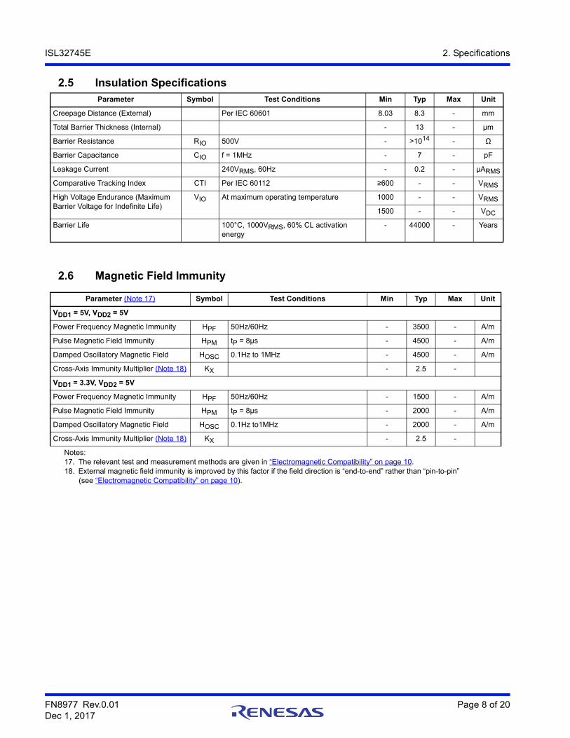
2.5 Insulation Specifications
2.6 Magnetic Field Immunity
Parameter Symbol Test Conditions Min Typ Max Unit
Creepage Distance (External) Per IEC 60601 8.03 8.3 - mm
Total Barrier Thickness (Internal) - 13 - µm
Barrier Resistance RIO 500V - >1014 - Ω
Barrier Capacitance CIO f = 1MHz - 7 - pF
Leakage Current 240VRMS, 60Hz - 0.2 - µARMS
Comparative Tracking Index CTI Per IEC 60112 ≥600 - - VRMS
High Voltage Endurance (Maximum Barrier Voltage for Indefinite Life)
VIO At maximum operating temperature 1000 - - VRMS
1500 - - VDC
Barrier Life 100°C, 1000VRMS, 60% CL activation energy
- 44000 - Years
Parameter (Note 17) Symbol Test Conditions Min Typ Max Unit
VDD1 = 5V, VDD2 = 5V
Power Frequency Magnetic Immunity HPF 50Hz/60Hz - 3500 - A/m
Pulse Magnetic Field Immunity HPM tP = 8µs - 4500 - A/m
Damped Oscillatory Magnetic Field HOSC 0.1Hz to 1MHz - 4500 - A/m
Cross-Axis Immunity Multiplier (Note 18) KX - 2.5 -
VDD1 = 3.3V, VDD2 = 5V
Power Frequency Magnetic Immunity HPF 50Hz/60Hz - 1500 - A/m
Pulse Magnetic Field Immunity HPM tP = 8µs - 2000 - A/m
Damped Oscillatory Magnetic Field HOSC 0.1Hz to1MHz - 2000 - A/m
Cross-Axis Immunity Multiplier (Note 18) KX - 2.5 -
Notes:17. The relevant test and measurement methods are given in “Electromagnetic Compatibility” on page 10.18. External magnetic field immunity is improved by this factor if the field direction is “end-to-end” rather than “pin-to-pin”
(see “Electromagnetic Compatibility” on page 10).
FN8977 Rev.0.01 Page 8 of 20Dec 1, 2017
ISL32745E 3. Safety and Approvals
3. Safety and Approvals
3.1 VDE V 0884-11 (Certification Pending)• Reinforced isolation; file number: certification pending
• Working voltage (VIORM) 1000VRMS (1415VPK); Reinforced insulation, Pollution degree 2
• Isolation voltage (VISO) 6000VRMS
• Surge immunity (VIOSM) 12.8kVPK
• Surge rating 8kV
• Transient overvoltage (VIOTM) 6000VPK
• Each part tested at 2387VPK for 1s, 5pC partial discharge limit
• Samples tested at 6000VPK for 60s, then 2122VPK for 10s with 5pC partial discharge limit
3.2 UL 1577 • Component Recognition Program File Number: E483309
• 6kV rating
• Each part tested at 7.2kVRMS (10.2kVPK) for 1s
• Each lot of samples tested at 6000VRMS (8485VPK) for 60s
Symbol Safety-Limiting Values Value Unit
TS Safety Rating Ambient Temperature +180 °C
PS Safety Rating Power (+180°C) 270 mW
IS Supply Current Safety Rating (total of supplies) 54 mA
FN8977 Rev.0.01 Page 9 of 20Dec 1, 2017
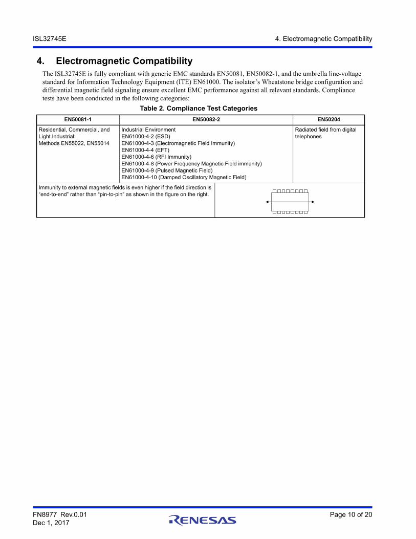
ISL32745E 4. Electromagnetic Compatibility
4. Electromagnetic CompatibilityThe ISL32745E is fully compliant with generic EMC standards EN50081, EN50082-1, and the umbrella line-voltage standard for Information Technology Equipment (ITE) EN61000. The isolator’s Wheatstone bridge configuration and differential magnetic field signaling ensure excellent EMC performance against all relevant standards. Compliance tests have been conducted in the following categories:
Table 2. Compliance Test Categories
EN50081-1 EN50082-2 EN50204
Residential, Commercial, and Light Industrial:Methods EN55022, EN55014
Industrial EnvironmentEN61000-4-2 (ESD)EN61000-4-3 (Electromagnetic Field Immunity)EN61000-4-4 (EFT)EN61000-4-6 (RFI Immunity)EN61000-4-8 (Power Frequency Magnetic Field immunity)EN61000-4-9 (Pulsed Magnetic Field)EN61000-4-10 (Damped Oscillatory Magnetic Field)
Radiated field from digital telephones
Immunity to external magnetic fields is even higher if the field direction is “end-to-end” rather than “pin-to-pin” as shown in the figure on the right.
FN8977 Rev.0.01 Page 10 of 20Dec 1, 2017
ISL32745E 5. Application Information
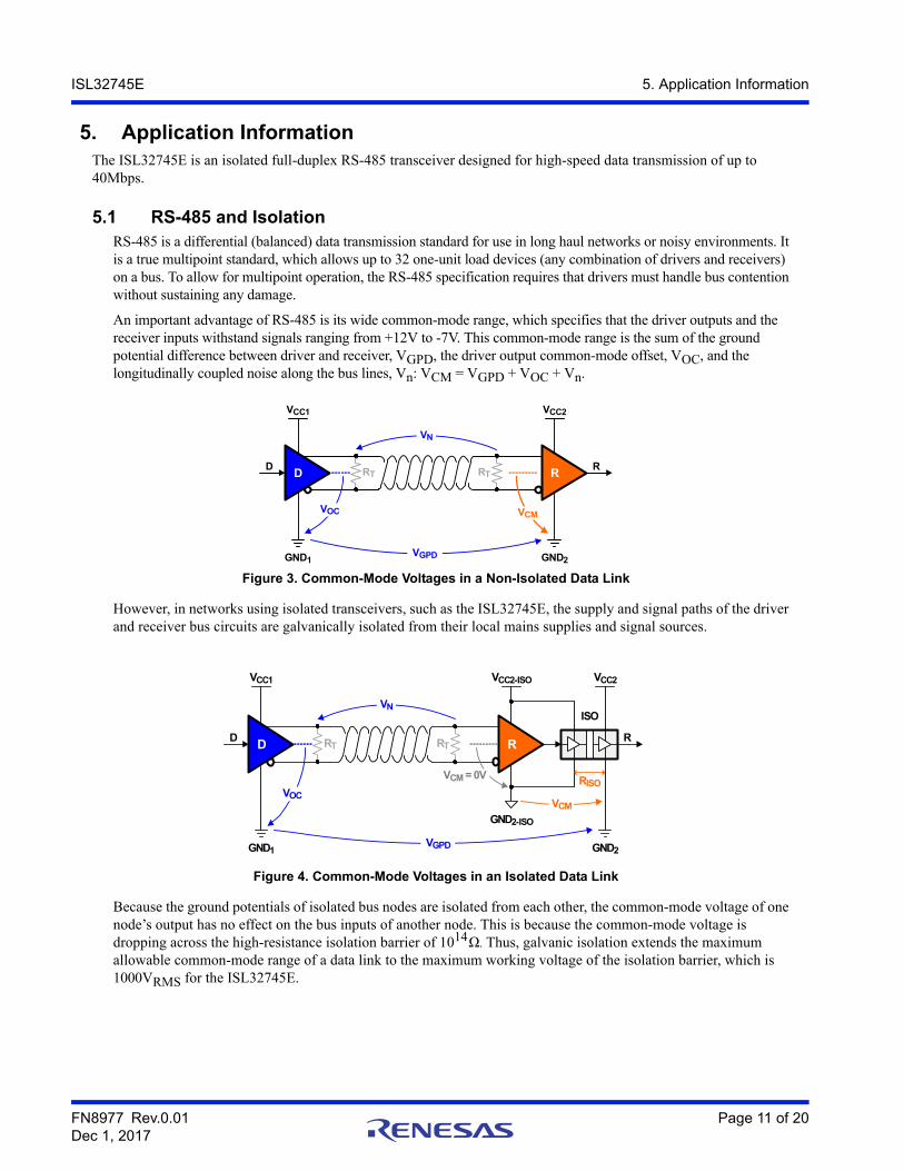
5. Application InformationThe ISL32745E is an isolated full-duplex RS-485 transceiver designed for high-speed data transmission of up to 40Mbps.
5.1 RS-485 and IsolationRS-485 is a differential (balanced) data transmission standard for use in long haul networks or noisy environments. It is a true multipoint standard, which allows up to 32 one-unit load devices (any combination of drivers and receivers) on a bus. To allow for multipoint operation, the RS-485 specification requires that drivers must handle bus contention without sustaining any damage.
An important advantage of RS-485 is its wide common-mode range, which specifies that the driver outputs and the receiver inputs withstand signals ranging from +12V to -7V. This common-mode range is the sum of the ground potential difference between driver and receiver, VGPD, the driver output common-mode offset, VOC, and the longitudinally coupled noise along the bus lines, Vn: VCM = VGPD + VOC + Vn.
However, in networks using isolated transceivers, such as the ISL32745E, the supply and signal paths of the driver and receiver bus circuits are galvanically isolated from their local mains supplies and signal sources.
Because the ground potentials of isolated bus nodes are isolated from each other, the common-mode voltage of one node’s output has no effect on the bus inputs of another node. This is because the common-mode voltage is dropping across the high-resistance isolation barrier of 1014Ω. Thus, galvanic isolation extends the maximum allowable common-mode range of a data link to the maximum working voltage of the isolation barrier, which is 1000VRMS for the ISL32745E.
Figure 3. Common-Mode Voltages in a Non-Isolated Data Link
Figure 4. Common-Mode Voltages in an Isolated Data Link
RT
VCC1
D
VGPD
R
GND2GND1
D R
VOC
RT
VCM
VN
VCC2
RT
VCC1
D
VGPD
R
GND2GND1
D
VOC
RT
VN
VCC2
ISO
VCC2-ISO
GND2-ISO
R
VCM = 0V
VCM
RISO
FN8977 Rev.0.01 Page 11 of 20Dec 1, 2017
ISL32745E 5. Application Information
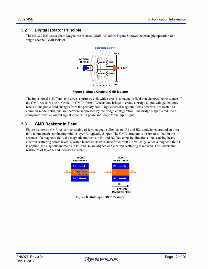
5.2 Digital Isolator PrincipleThe ISL32745E uses a Giant Magnetoresistance (GMR) isolation. Figure 5 shows the principle operation of a single channel GMR isolator.
The input signal is buffered and drives a primary coil, which creates a magnetic field that changes the resistance of the GMR resistors 1 to 4. GMR1 to GMR4 form a Wheatstone bridge to create a bridge output voltage that only reacts to magnetic field changes from the primary coil. Large external magnetic fields however, are treated as common-mode fields, and are therefore suppressed by the bridge configuration. The bridge output is fed into a comparator with an output signal identical in phase and shape to the input signal.
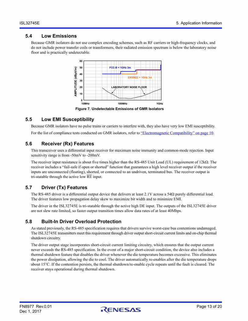
5.3 GMR Resistor in DetailFigure 6 shows a GMR resistor consisting of ferromagnetic alloy layers, B1 and B2, sandwiched around an ultra thin, nonmagnetic conducting middle layer A, typically copper. The GMR structure is designed so that, in the absence of a magnetic field, the magnetic moments in B1 and B2 face opposite directions, thus causing heavy electron scattering across layer A, which increases its resistance for current C drastically. When a magnetic field D is applied, the magnetic moments in B1 and B2 are aligned and electron scattering is reduced. This lowers the resistance of layer A and increases current C.
Figure 5. Single Channel GMR Isolator
Figure 6. Multilayer GMR Resistor
IN
VDD2
GND2
OUT
EXTERNAL B-FIELD
INTERNALB-FIELD GMR2
GMR4GMR3
GMR1
B1
A
B2
C
B1
A
B2
C C
D
APPLIED MAGNETIC FIELD
HIGH RESISTANCE
LOW RESISTANCE
C
FN8977 Rev.0.01 Page 12 of 20Dec 1, 2017
ISL32745E 5. Application Information
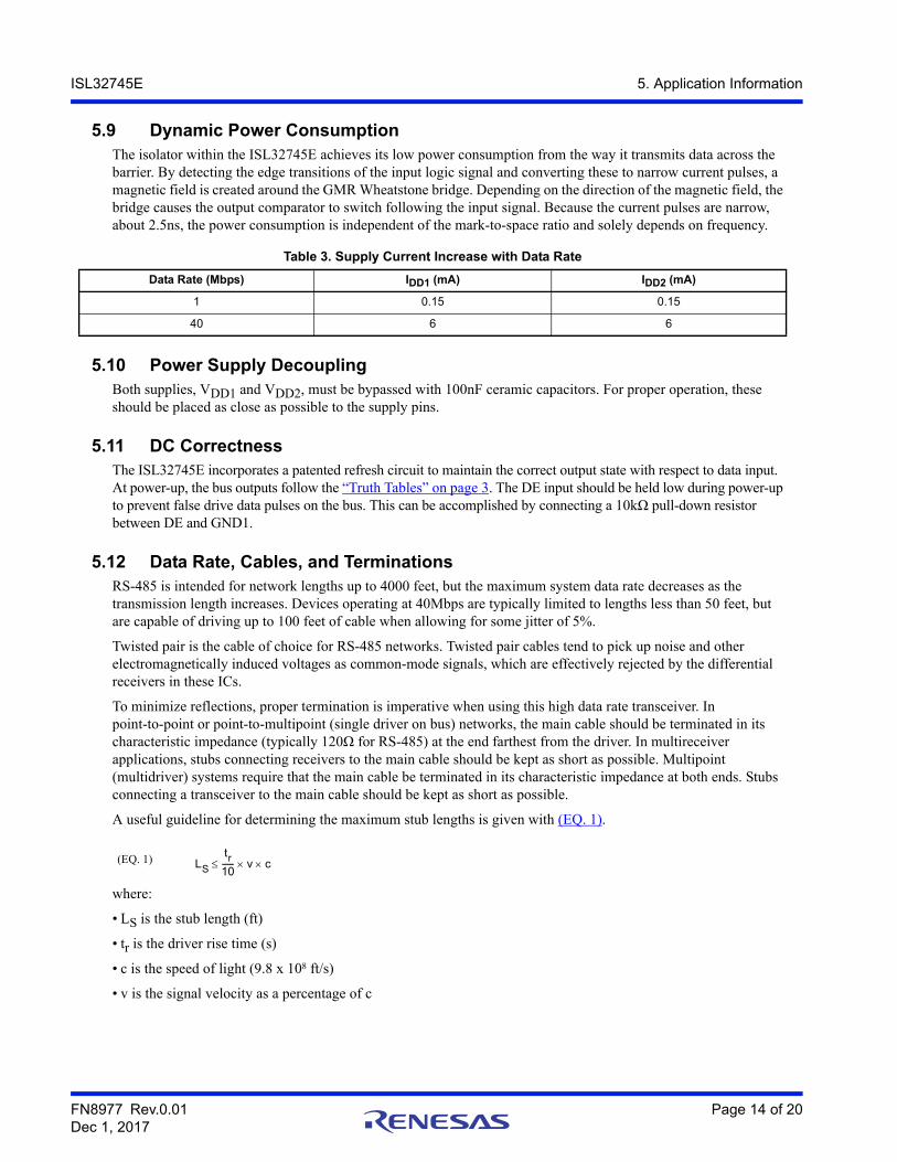
5.4 Low EmissionsBecause GMR isolators do not use complex encoding schemes, such as RF carriers or high-frequency clocks, and do not include power transfer coils or transformers, their radiated emission spectrum is below the laboratory noise floor and is practically undetectable.
5.5 Low EMI SusceptibilityBecause GMR isolators have no pulse trains or carriers to interfere with, they also have very low EMI susceptibility.
For the list of compliance tests conducted on GMR isolators, refer to “Electromagnetic Compatibility” on page 10.
5.6 Receiver (Rx) FeaturesThis transceiver uses a differential input receiver for maximum noise immunity and common-mode rejection. Input sensitivity range is from -50mV to -200mV.
The receiver input resistance is about five times higher than the RS-485 Unit Load (UL) requirement of 12kΩ. The receiver includes a “fail-safe if open or shorted” function that guarantees a high level receiver output if the receiver inputs are unconnected (floating), shorted, or connected to an undriven, terminated bus. The receiver output is tri-statable through the active low RE input.
5.7 Driver (Tx) FeaturesThe RS-485 driver is a differential output device that delivers at least 2.1V across a 54Ω purely differential load. The driver features low propagation delay skew to maximize bit width and to minimize EMI.
The driver in the ISL32745E is tri-statable through the active high DE input. The outputs of the ISL32745E driver are not slew rate limited, so faster output transition times allow data rates of at least 40Mbps.
5.8 Built-In Driver Overload ProtectionAs stated previously, the RS-485 specification requires that drivers survive worst-case bus contentions undamaged. The ISL32745E transmitters meet this requirement through driver output short-circuit current limits and on-chip thermal shutdown circuitry.
The driver output stage incorporates short-circuit current limiting circuitry, which ensures that the output current never exceeds the RS-485 specification. In the event of a major short-circuit condition, the device also includes a thermal shutdown feature that disables the driver whenever the die temperature becomes excessive. This eliminates the power dissipation, allowing the die to cool. The driver automatically re-enables after the die temperature drops about 15°C. If the contention persists, the thermal shutdown/re-enable cycle repeats until the fault is cleared. The receiver stays operational during thermal shutdown.
Figure 7. Undetectable Emissions of GMR Isolators
AM
PL
ITU
DE
(d
Bµ
V/m
) FCC-B < 1GHz 3m
EN55022 < 1GHz 3m
LABORATORY NOISE FLOOR
10MHz 100MHz 1GHz
60
50
40
30
20
10
0
FN8977 Rev.0.01 Page 13 of 20Dec 1, 2017
ISL32745E 5. Application Information
5.9 Dynamic Power ConsumptionThe isolator within the ISL32745E achieves its low power consumption from the way it transmits data across the barrier. By detecting the edge transitions of the input logic signal and converting these to narrow current pulses, a magnetic field is created around the GMR Wheatstone bridge. Depending on the direction of the magnetic field, the bridge causes the output comparator to switch following the input signal. Because the current pulses are narrow, about 2.5ns, the power consumption is independent of the mark-to-space ratio and solely depends on frequency.
5.10 Power Supply DecouplingBoth supplies, VDD1 and VDD2, must be bypassed with 100nF ceramic capacitors. For proper operation, these should be placed as close as possible to the supply pins.
5.11 DC CorrectnessThe ISL32745E incorporates a patented refresh circuit to maintain the correct output state with respect to data input. At power-up, the bus outputs follow the “Truth Tables” on page 3. The DE input should be held low during power-up to prevent false drive data pulses on the bus. This can be accomplished by connecting a 10kΩ pull-down resistor between DE and GND1.
5.12 Data Rate, Cables, and Terminations RS-485 is intended for network lengths up to 4000 feet, but the maximum system data rate decreases as the transmission length increases. Devices operating at 40Mbps are typically limited to lengths less than 50 feet, but are capable of driving up to 100 feet of cable when allowing for some jitter of 5%.
Twisted pair is the cable of choice for RS-485 networks. Twisted pair cables tend to pick up noise and other electromagnetically induced voltages as common-mode signals, which are effectively rejected by the differential receivers in these ICs.
To minimize reflections, proper termination is imperative when using this high data rate transceiver. In point-to-point or point-to-multipoint (single driver on bus) networks, the main cable should be terminated in its characteristic impedance (typically 120Ω for RS-485) at the end farthest from the driver. In multireceiver applications, stubs connecting receivers to the main cable should be kept as short as possible. Multipoint (multidriver) systems require that the main cable be terminated in its characteristic impedance at both ends. Stubs connecting a transceiver to the main cable should be kept as short as possible.
A useful guideline for determining the maximum stub lengths is given with (EQ. 1).
where:
• LS is the stub length (ft)
• tr is the driver rise time (s)
• c is the speed of light (9.8 x 108 ft/s)
• v is the signal velocity as a percentage of c
Table 3. Supply Current Increase with Data Rate
Data Rate (Mbps) IDD1 (mA) IDD2 (mA)
1 0.15 0.15
40 6 6
(EQ. 1) LS
tr10------ v c
FN8977 Rev.0.01 Page 14 of 20Dec 1, 2017
ISL32745E 5. Application Information
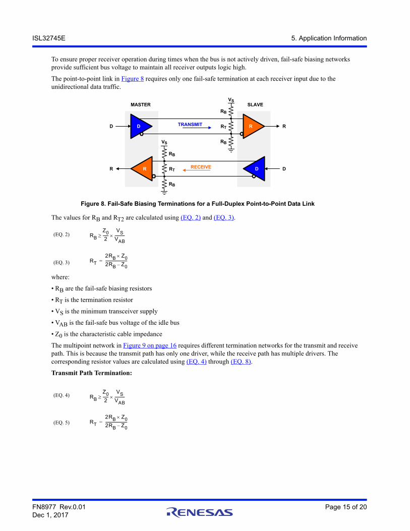
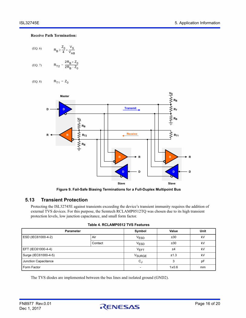
To ensure proper receiver operation during times when the bus is not actively driven, fail-safe biasing networks provide sufficient bus voltage to maintain all receiver outputs logic high.
The point-to-point link in Figure 8 requires only one fail-safe termination at each receiver input due to the unidirectional data traffic.
The values for RB and RT2 are calculated using (EQ. 2) and (EQ. 3).
where:
• RB are the fail-safe biasing resistors
• RT is the termination resistor
• VS is the minimum transceiver supply
• VAB is the fail-safe bus voltage of the idle bus
• Z0 is the characteristic cable impedance
The multipoint network in Figure 9 on page 16 requires different termination networks for the transmit and receive path. This is because the transmit path has only one driver, while the receive path has multiple drivers. The corresponding resistor values are calculated using (EQ. 4) through (EQ. 8).
Transmit Path Termination:
Figure 8. Fail-Safe Biasing Terminations for a Full-Duplex Point-to-Point Data Link
RT
RT
MASTER
TRANSMIT
RECEIVE
VS
RB
RBVS
RB
RB
DD
D
R
RR
R
D
SLAVE
(EQ. 2) RB
Z02
------VS
VAB-----------
(EQ. 3) RT
2RB Z0
2RB Z0–------------------------=
(EQ. 4) RB
Z02
------VS
VAB-----------
(EQ. 5) RT
2RB Z0
2RB Z0–------------------------=
FN8977 Rev.0.01 Page 15 of 20Dec 1, 2017
ISL32745E 5. Application Information
Receive Path Termination:
5.13 Transient Protection Protecting the ISL32745E against transients exceeding the device’s transient immunity requires the addition of external TVS devices. For this purpose, the Semtech RCLAMP0512TQ was chosen due to its high transient protection levels, low junction capacitance, and small form factor.
The TVS diodes are implemented between the bus lines and isolated ground (GND2).
Figure 9. Fail-Safe Biasing Terminations for a Full-Duplex Multipoint Bus
Table 4. RCLAMP0512 TVS Features
Parameter Symbol Value Unit
ESD (IEC61000-4-2) Air VESD ±30 kV
Contact VESD ±30 kV
EFT (IEC61000-4-4) VEFT ±4 kV
Surge (IEC61000-4-5) VSURGE ±1.3 kV
Junction Capacitance CJ 3 pF
Form Factor - 1x0.6 mm
(EQ. 6) RB
Z04
------VS
VAB-----------
(EQ. 7) RT2
2RB Z0
2RB Z0–------------------------=
(EQ. 8) RT1 Z0=
RT2
Master
VS
RB
RB
DD
RR
D
R R
D
Slave
Receive
Transmit RT
VS
RB
RB
D
R R
D
Slave
RT1
FN8977 Rev.0.01 Page 16 of 20Dec 1, 2017
ISL32745E 5. Application Information
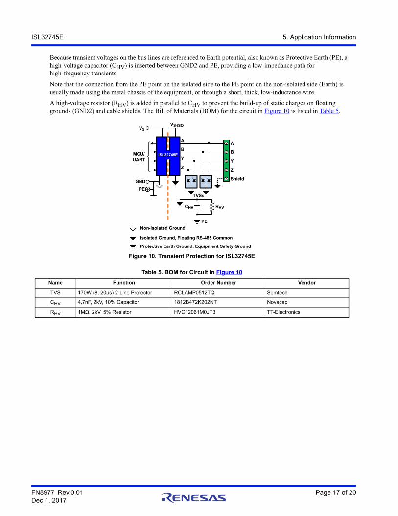
Because transient voltages on the bus lines are referenced to Earth potential, also known as Protective Earth (PE), a high-voltage capacitor (CHV) is inserted between GND2 and PE, providing a low-impedance path for high-frequency transients.
Note that the connection from the PE point on the isolated side to the PE point on the non-isolated side (Earth) is usually made using the metal chassis of the equipment, or through a short, thick, low-inductance wire.
A high-voltage resistor (RHV) is added in parallel to CHV to prevent the build-up of static charges on floating grounds (GND2) and cable shields. The Bill of Materials (BOM) for the circuit in Figure 10 is listed in Table 5.
Figure 10. Transient Protection for ISL32745E
Table 5. BOM for Circuit in Figure 10
Name Function Order Number Vendor
TVS 170W (8, 20µs) 2-Line Protector RCLAMP0512TQ Semtech
CHV 4.7nF, 2kV, 10% Capacitor 1812B472K202NT Novacap
RHV 1MΩ, 2kV, 5% Resistor HVC12061M0JT3 TT-Electronics
MCU/UART
VS-ISO
B
A
VS
GND
PE
RHVCHV
Z
Y
Shield
TVSs
ISL32745E
PE
Protective Earth Ground, Equipment Safety Ground
Isolated Ground, Floating RS-485 Common
Non-isolated Ground
Z
YB
A
FN8977 Rev.0.01 Page 17 of 20Dec 1, 2017
ISL32745E 6. Revision History
6. Revision History
Rev. Date Description
0.00 Dec 1, 2017 Initial release.
FN8977 Rev.0.01 Page 18 of 20Dec 1, 2017
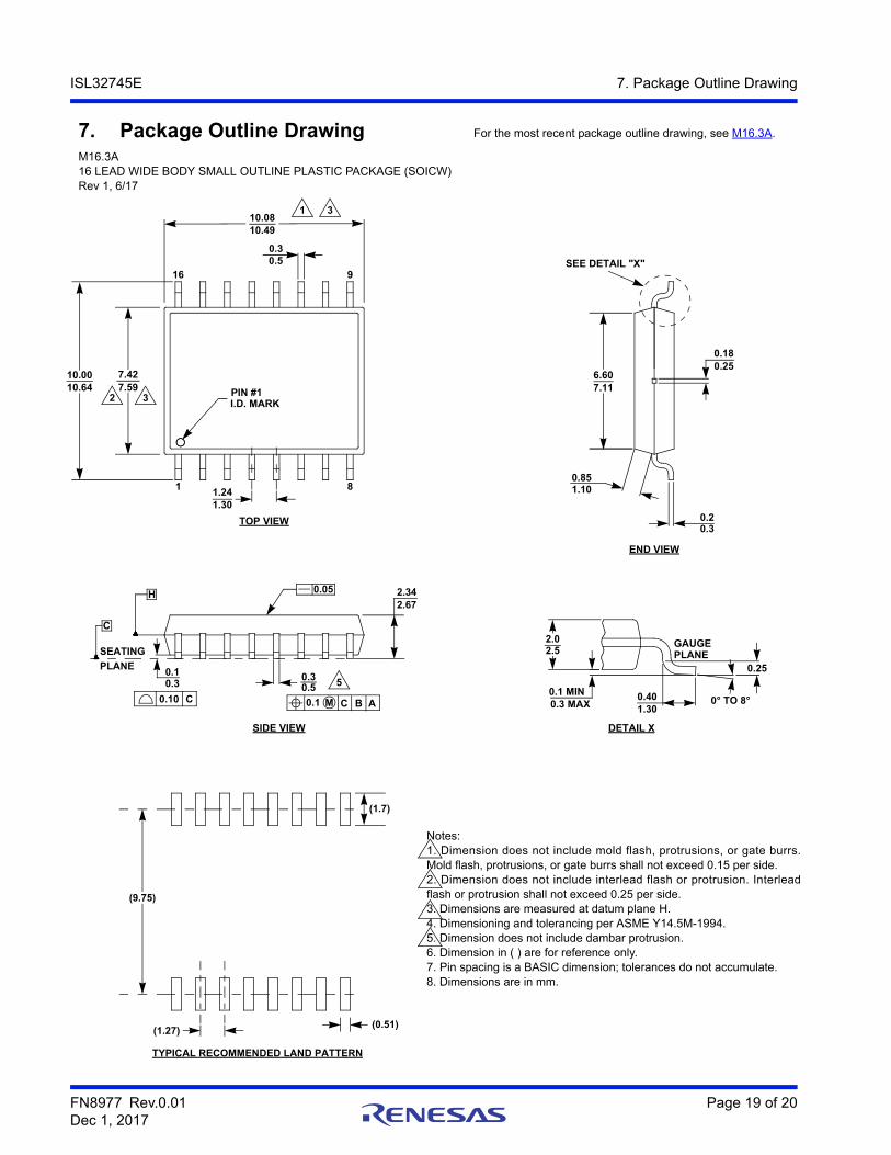
ISL32745E 7. Package Outline Drawing
.
7. Package Outline DrawingM16.3A16 LEAD WIDE BODY SMALL OUTLINE PLASTIC PACKAGE (SOICW)Rev 1, 6/17
END VIEW
16
1 8
9
PIN #1I.D. MARK
SIDE VIEW
TYPICAL RECOMMENDED LAND PATTERN
0.3 MAX0.1 MIN
DETAIL X
GAUGE
0.05
TOP VIEW
SEATING
PLANE
C
H
SEE DETAIL "X"
0.30.5
1.241.30
0.851.10
0.20.3
0.180.25
0.30.5
0.40 0° TO 8°
0.25
1.30
2.342.67
0.10.3
(0.51)(1.27)
0.10 C 0.1 C BM A
1 3
2 3
5
10.0810.49
10.0010.64
7.427.59
6.607.11
PLANE
2.02.5
(1.7)
(9.75)
Notes:1. Dimension does not include mold flash, protrusions, or gate burrsMold flash, protrusions, or gate burrs shall not exceed 0.15 per side.2. Dimension does not include interlead flash or protrusion. Interleadflash or protrusion shall not exceed 0.25 per side.3. Dimensions are measured at datum plane H.4. Dimensioning and tolerancing per ASME Y14.5M-1994.5. Dimension does not include dambar protrusion.6. Dimension in ( ) are for reference only.7. Pin spacing is a BASIC dimension; tolerances do not accumulate.8. Dimensions are in mm.
For the most recent package outline drawing, see M16.3A.
FN8977 Rev.0.01 Page 19 of 20Dec 1, 2017
http://www.renesas.comRefer to "http://www.renesas.com/" for the latest and detailed information.
Renesas Electronics America Inc.1001 Murphy Ranch Road, Milpitas, CA 95035, U.S.A.Tel: +1-408-432-8888, Fax: +1-408-434-5351Renesas Electronics Canada Limited9251 Yonge Street, Suite 8309 Richmond Hill, Ontario Canada L4C 9T3Tel: +1-905-237-2004Renesas Electronics Europe LimitedDukes Meadow, Millboard Road, Bourne End, Buckinghamshire, SL8 5FH, U.KTel: +44-1628-651-700, Fax: +44-1628-651-804Renesas Electronics Europe GmbHArcadiastrasse 10, 40472 Düsseldorf, Germany Tel: +49-211-6503-0, Fax: +49-211-6503-1327Renesas Electronics (China) Co., Ltd.Room 1709 Quantum Plaza, No.27 ZhichunLu, Haidian District, Beijing, 100191 P. R. ChinaTel: +86-10-8235-1155, Fax: +86-10-8235-7679Renesas Electronics (Shanghai) Co., Ltd.Unit 301, Tower A, Central Towers, 555 Langao Road, Putuo District, Shanghai, 200333 P. R. China Tel: +86-21-2226-0888, Fax: +86-21-2226-0999Renesas Electronics Hong Kong LimitedUnit 1601-1611, 16/F., Tower 2, Grand Century Place, 193 Prince Edward Road West, Mongkok, Kowloon, Hong KongTel: +852-2265-6688, Fax: +852 2886-9022Renesas Electronics Taiwan Co., Ltd.13F, No. 363, Fu Shing North Road, Taipei 10543, TaiwanTel: +886-2-8175-9600, Fax: +886 2-8175-9670Renesas Electronics Singapore Pte. Ltd.80 Bendemeer Road, Unit #06-02 Hyflux Innovation Centre, Singapore 339949Tel: +65-6213-0200, Fax: +65-6213-0300Renesas Electronics Malaysia Sdn.Bhd.Unit 1207, Block B, Menara Amcorp, Amcorp Trade Centre, No. 18, Jln Persiaran Barat, 46050 Petaling Jaya, Selangor Darul Ehsan, MalaysiaTel: +60-3-7955-9390, Fax: +60-3-7955-9510Renesas Electronics India Pvt. Ltd.No.777C, 100 Feet Road, HAL 2nd Stage, Indiranagar, Bangalore 560 038, IndiaTel: +91-80-67208700, Fax: +91-80-67208777Renesas Electronics Korea Co., Ltd.17F, KAMCO Yangjae Tower, 262, Gangnam-daero, Gangnam-gu, Seoul, 06265 KoreaTel: +82-2-558-3737, Fax: +82-2-558-5338
SALES OFFICES
© 2018 Renesas Electronics Corporation. All rights reserved.Colophon 7.0
(Rev.4.0-1 November 2017)
Notice
1. Descriptions of circuits, software and other related information in this document are provided only to illustrate the operation of semiconductor products and application examples. You are fully responsible for
the incorporation or any other use of the circuits, software, and information in the design of your product or system. Renesas Electronics disclaims any and all liability for any losses and damages incurred by
you or third parties arising from the use of these circuits, software, or information.
2. Renesas Electronics hereby expressly disclaims any warranties against and liability for infringement or any other claims involving patents, copyrights, or other intellectual property rights of third parties, by or
arising from the use of Renesas Electronics products or technical information described in this document, including but not limited to, the product data, drawings, charts, programs, algorithms, and application
examples.
3. No license, express, implied or otherwise, is granted hereby under any patents, copyrights or other intellectual property rights of Renesas Electronics or others.
4. You shall not alter, modify, copy, or reverse engineer any Renesas Electronics product, whether in whole or in part. Renesas Electronics disclaims any and all liability for any losses or damages incurred by
you or third parties arising from such alteration, modification, copying or reverse engineering.
5. Renesas Electronics products are classified according to the following two quality grades: “Standard” and “High Quality”. The intended applications for each Renesas Electronics product depends on the
product’s quality grade, as indicated below.
"Standard": Computers; office equipment; communications equipment; test and measurement equipment; audio and visual equipment; home electronic appliances; machine tools; personal electronic
equipment; industrial robots; etc.
"High Quality": Transportation equipment (automobiles, trains, ships, etc.); traffic control (traffic lights); large-scale communication equipment; key financial terminal systems; safety control equipment; etc.
Unless expressly designated as a high reliability product or a product for harsh environments in a Renesas Electronics data sheet or other Renesas Electronics document, Renesas Electronics products are
not intended or authorized for use in products or systems that may pose a direct threat to human life or bodily injury (artificial life support devices or systems; surgical implantations; etc.), or may cause
serious property damage (space system; undersea repeaters; nuclear power control systems; aircraft control systems; key plant systems; military equipment; etc.). Renesas Electronics disclaims any and all
liability for any damages or losses incurred by you or any third parties arising from the use of any Renesas Electronics product that is inconsistent with any Renesas Electronics data sheet, user’s manual or
other Renesas Electronics document.
6. When using Renesas Electronics products, refer to the latest product information (data sheets, user’s manuals, application notes, “General Notes for Handling and Using Semiconductor Devices” in the
reliability handbook, etc.), and ensure that usage conditions are within the ranges specified by Renesas Electronics with respect to maximum ratings, operating power supply voltage range, heat dissipation
characteristics, installation, etc. Renesas Electronics disclaims any and all liability for any malfunctions, failure or accident arising out of the use of Renesas Electronics products outside of such specified
ranges.
7. Although Renesas Electronics endeavors to improve the quality and reliability of Renesas Electronics products, semiconductor products have specific characteristics, such as the occurrence of failure at a
certain rate and malfunctions under certain use conditions. Unless designated as a high reliability product or a product for harsh environments in a Renesas Electronics data sheet or other Renesas
Electronics document, Renesas Electronics products are not subject to radiation resistance design. You are responsible for implementing safety measures to guard against the possibility of bodily injury, injury
or damage caused by fire, and/or danger to the public in the event of a failure or malfunction of Renesas Electronics products, such as safety design for hardware and software, including but not limited to
redundancy, fire control and malfunction prevention, appropriate treatment for aging degradation or any other appropriate measures. Because the evaluation of microcomputer software alone is very difficult
and impractical, you are responsible for evaluating the safety of the final products or systems manufactured by you.
8. Please contact a Renesas Electronics sales office for details as to environmental matters such as the environmental compatibility of each Renesas Electronics product. You are responsible for carefully and
sufficiently investigating applicable laws and regulations that regulate the inclusion or use of controlled substances, including without limitation, the EU RoHS Directive, and using Renesas Electronics
products in compliance with all these applicable laws and regulations. Renesas Electronics disclaims any and all liability for damages or losses occurring as a result of your noncompliance with applicable
laws and regulations.
9. Renesas Electronics products and technologies shall not be used for or incorporated into any products or systems whose manufacture, use, or sale is prohibited under any applicable domestic or foreign laws
or regulations. You shall comply with any applicable export control laws and regulations promulgated and administered by the governments of any countries asserting jurisdiction over the parties or
transactions.
10. It is the responsibility of the buyer or distributor of Renesas Electronics products, or any other party who distributes, disposes of, or otherwise sells or transfers the product to a third party, to notify such third
party in advance of the contents and conditions set forth in this document.
11. This document shall not be reprinted, reproduced or duplicated in any form, in whole or in part, without prior written consent of Renesas Electronics.
12. Please contact a Renesas Electronics sales office if you have any questions regarding the information contained in this document or Renesas Electronics products.
(Note 1) “Renesas Electronics” as used in this document means Renesas Electronics Corporation and also includes its directly or indirectly controlled subsidiaries.
(Note 2) “Renesas Electronics product(s)” means any product developed or manufactured by or for Renesas Electronics.