Embed Size (px)
Citation preview

TEST REPORT
AN1949Rev 0.00
July 31, 2014
ISL70419SEHTotal Dose Testing
IntroductionThis document reports the results of low and high dose rate total dose testing of the ISL70419SEH quad operational amplifier. The tests were conducted to provide an assessment of the total dose hardness of the part. Parts were irradiated under bias and with all pins grounded at low and high dose rate. A 168-hour biased anneal at +100°C was performed on the high dose rate samples after the completion of irradiations. A similar anneal (of half the samples) was performed on a sampling basis (half the samples, or 6 parts) on the low dose rate samples after 50 krad(Si), while the remaining post low dose rate anneal will be performed on the rest of the samples after the 100 krad(Si) downpoint. The ISL70419SEH is acceptance tested on a wafer-by-wafer basis to 300 krad(Si) at high dose rate (50 to 300 rad(Si)/s) and to 50 krad(Si) at low dose rate (0.01 rad(Si)/s).
Reference DocumentsMIL-STD-883 test method 1019
ISL70419SEH data sheet.
Part DescriptionThe ISL70419SEH is a precision quad operational amplifier featuring low noise vs power consumption characteristics, low offset voltage, low input bias current and low temperature drift, making this device the ideal choice for hardened applications requiring high DC accuracy and moderate AC performance. The ISL70419SEH is offered in a 14 Ld Hermetic package and are specified over the -55°C to +125°C temperature range. Constructed with Intersil's dielectrically isolated PR40 process, this device is immune to single-event latch-up and features improved single-event transient (SET) performance. The ISL70419SEH offers guaranteed performance over the full -55°C to +125°C military temperature range. Key pre- and post-radiation specifications follow.
• Input offset voltage. . . . ±85µV pre, ±110µV post, maximum
• Input bias current . . . ±2.5 nA pre, ±15.0nA post, maximum
• Supply current, each amplifier . . . . 625µA pre, 750µA post, maximum
• Voltage noise . . . . . . . . . . . . . . . . . . . . . . . . 8nV/Hz maximum
• Common mode rejection ratio . . . . . . . . . . 120dB minimum
• Power supply rejection ratio . . . . . . . . . . . . 120dB minimum
• Open-loop gain . . . . . . . . . .129.5dB minimum (3000 V/mV)
• Supply voltage range . . . . . . . . . . . . . . . 4.5V to 36V in beam (86.4MeV.cm2/mg Au)
• Operating temperature range . . . . . . . . . . . -55°C to +125°C
Test DescriptionIrradiation FacilitiesHigh dose rate testing was performed at 65 rad(Si)/s using a Gammacell 220 60Co irradiator located in the Palm Bay, Florida Intersil facility. Low dose rate testing was performed at 0.01rad(Si)/s using the Intersil Palm Bay N40 panoramic 60Co low dose rate irradiator.
Test Fixturing
Figure 2 shows the configuration used for biased irradiation.
FIGURE 1. ISL70419SEH BLOCK DIAGRAM
+-
+-
+
-
+-
OUTPUT 1
-INPUT 1
+INPUT 1
+VCC
+INPUT 2
-INPUT 2
OUTPUT 2 OUTPUT 3
OUTPUT 4
-INPUT 3
-INPUT 4
+INPUT 3
+INPUT 4
-VCC
FIGURE 2. IRRADIATION BIAS CONFIGURATION FOR THE ISL70419SEH
VEE (V2)VCC (V1)
OUTPUTA
VIN A
VIP A
VCC
VIP B
VIN B
OUTPUTB OUTPUTC
VIN C
VIP C
VEE
VIP B
VIN B
OUTPUTB1
2
3
4
5
6
7 8
9
10
11
12
13
14DUT
AN1949 Rev 0.00 Page 1 of 13July 31, 2014

ISL70419SEH Total Dose Testing
Characterization Equipment and ProceduresAll electrical testing was performed outside the irradiator using the production automated test equipment (ATE) with data logging at each downpoint. Downpoint electrical testing was performed at room temperature. Postirradiation anneals were performed using a small temperature chamber.
Experimental MatrixTotal dose irradiation proceeded in accordance with the guidelines of MIL-STD-883 Test Method 1019.7. The experimental matrix consisted of 12 samples irradiated at low dose rate under bias, 12 samples irradiated at low dose rate with all pins grounded, 12 samples irradiated at high dose rate under bias and 12 samples irradiated at high dose rate with all pins grounded. Three control units were used to insure repeatable data. Irradiations were followed by a biased high temperature anneal at +100°C for 168 hours; the anneal is complete for the high dose rate samples and half the low dose rate samples. The final anneal will be performed on the remaining (six) low dose rate samples following the completion of irradiation to 100 krad(Si). The test is structured in this manner to account for the fact that once annealed, the samples cannot be irradiated again as the previously incurred radiation damage is now annealed out, or at least partially annealed out. The resulting data would clearly be invalid.
Samples of the ISL70419SEH were drawn from PR40 fabrication lot X0H6D and were packaged in the hermetic 14-pin solder-sealed flatpack (CDFP4-F14, code KCK) package. Samples were processed through the standard burn-in cycle before irradiation, as required by MIL-STD-883, and were screened to the ATE limits at room temperature prior to the test.
DownpointsDownpoints to date for the low dose rate tests were zero, 10, 30 and 50 krad(Si), with a further planned downpoint at 100 krad(Si). Downpoints for the high dose rate tests were 0, 30, 50, 100, 300 and 450 krad(Si). The 450 krad(Si) level represent the 50% overtest over the part's SMD rated total dose level of 300 krad(Si), as per Method 1019. The post high dose rate anneal and the sample post low dose rate anneal are complete, while the remaining post low dose rate anneal will be performed after the 100 krad(Si) downpoint.
Test ResultsTesting at low and high dose rate of the ISL70419SEH is complete. All parts met the SMD post-radiation specifications at all downpoints. No differences in total dose response were noted between biased and grounded irradiation for any parameters. Additionally, no channel-to-channel differences were noted, either in the preirradiation data or in the total dose response of the parts. We did note dose rate sensitivity in the input bias current and input offset current results and the part is considered dose rate sensitive. The ISL70419SEH is acceptance tested on a wafer-by-wafer basis to 300 krad(Si) at high dose rate (50 to 300 rad(Si)/s) and to 50 krad(Si) at low dose rate (0.01 rad(Si)/s, providing hardness assurance at both dose rates. Table 1 summarizes the results.
TABLE 1. ISL71091SEH TOTAL DOSE TEST ATTRIBUTES DATA
PARTDOSE RATE
(Note 1) BIASSAMPLE
SIZE DOWNPOINTPASS
(Note 2) REJECTS
ISL70419SEH LDR Biased 12 Preirradiation 12
10 krad(Si) 12 0
30 krad(Si) 12 0
50 krad(Si) 12 0
Anneal 6 0
100 krad(Si) TBD TBD
Anneal TBD TBD
ISL70419SEH LDR Grounded 12 Preirradiation 12
10 krad(Si) 12 0
30 krad(Si) 12 0
50 krad(Si) 12 0
Anneal 6 0
100 krad(Si) TBD TBD
Anneal TBD TBD
AN1949 Rev 0.00 Page 2 of 13July 31, 2014

ISL70419SEH Total Dose Testing
ISL70419SEH HDR Biased 12 Preirradiation 12
30 krad(Si) 12 0
50 krad(Si) 12 0
100 krad(Si) 12 0
300 krad(Si) 12 0
450 krad(Si) 12 0
Anneal 12 0
ISL70419SEH HDR Grounded 12 Preirradiation 12
30 krad(Si) 12 0
50 krad(Si) 12 0
100 krad(Si) 12 0
300 krad(Si) 12 0
450 krad(Si) 12 0
Anneal 12 0
NOTES:
1. HDR indicates high dose rate (50 to 300 rad(Si)/s) as specified in MIL-STD-883 TM1019; the actual dose rate for these tests was 65 rad(Si)/s. LDR indicates low dose rate (0.01 rad(Si)/s), also as specified in TM1019.
2. “Pass” indicates a sample that passes all postirradiation SMD limits.
TABLE 1. ISL71091SEH TOTAL DOSE TEST ATTRIBUTES DATA (Continued)
PARTDOSE RATE
(Note 1) BIASSAMPLE
SIZE DOWNPOINTPASS
(Note 2) REJECTS
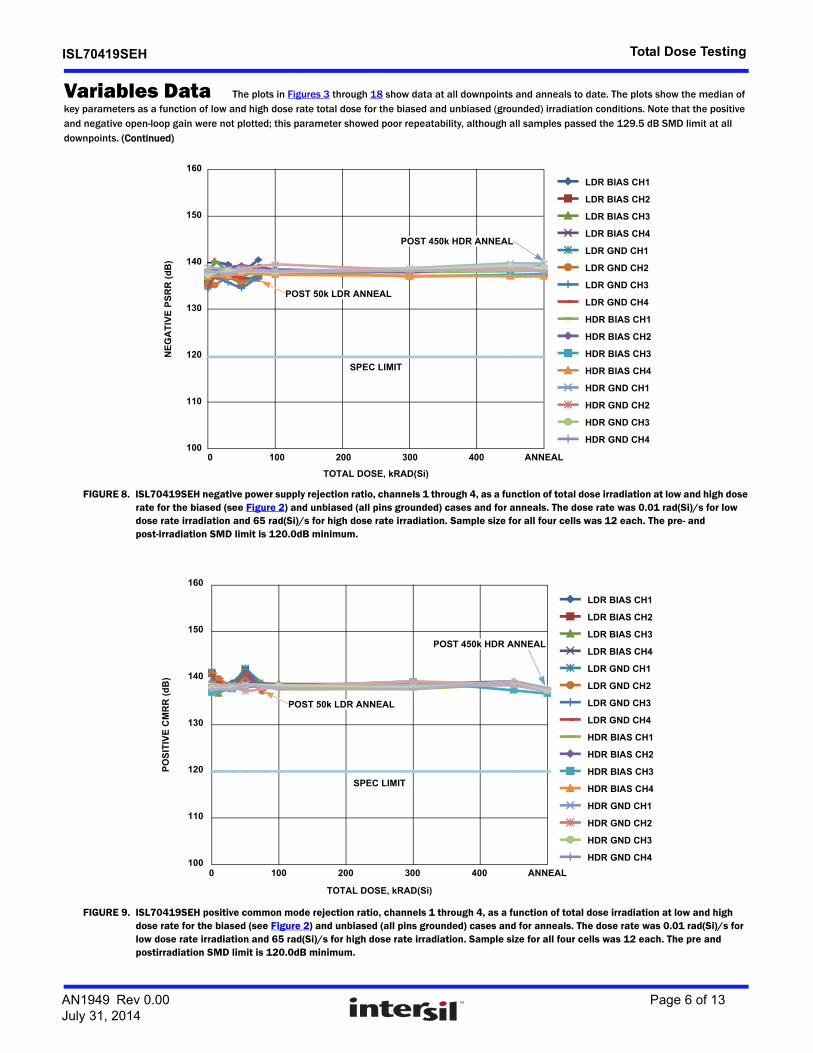
Variables Data The plots in Figures 3 through 18 show data at all downpoints and anneals to date. The plots show the median of key parameters as a function of low and high dose rate total dose for the biased and unbiased (grounded) irradiation conditions. Note that the positive and negative open-loop gain were not plotted; this parameter showed poor repeatability, although all samples passed the 129.5 dB SMD limit at all downpoints.
FIGURE 3. ISL70419SEH input offset voltage, channels 1 through 4, as a function of total dose irradiation at low and high dose rate for the biased (see Figure 2) and unbiased (all pins grounded) cases and for anneals. The dose rate was 0.01 rad(Si)/s for low dose rate irradiation and 65 rad(Si)/s for high dose rate irradiation. Sample size for all four cells was 12 each. The preirradiation SMD limits are -85µV to +85µV, while the postirradiation SMD limits are -110µV to +110µV.
-150
-100
-50
0
50
100
150
0 100 200 300 400 ANNEAL
TOTAL DOSE, krad(Si)
INP
UT
OF
FS
ET
VO
LT
AG
E (
µV
)
HDR GND CH4
HDR GND CH3
HDR GND CH2
HDR GND CH1
HDR BIAS CH4
HDR BIAS CH3
HDR BIAS CH2
HDR BIAS CH1
LDR GND CH4
LDR GND CH3
LDR GND CH2
LDR GND CH1
LDR BIAS CH4
LDR BIAS CH3
LDR BIAS CH2
LDR BIAS CH1
SPEC LIMIT
SPEC LIMIT
POST 450k HDR ANNEAL
POST 50k LDR ANNEAL
AN1949 Rev 0.00 Page 3 of 13July 31, 2014

ISL70419SEH Total Dose Testing
FIGURE 4. ISL70419SEH positive input bias current, channels 1 through 4, as a function of total dose irradiation at low and high dose rate for the biased (see Figure 2) and unbiased (all pins grounded) cases and for anneals. The dose rate was 0.01 rad(Si)/s for low dose rate irradiation and 65 rad(Si)/s for high dose rate irradiation. Sample size for all four cells was 12 each. The preirradiation SMD limits are -2.5nA to +2.5nA, while the postirradiation SMD limits are -15.0nA to +15.0nA.
FIGURE 5. ISL70419SEH negative input bias current, channels 1 through 4, as a function of total dose irradiation at low and high dose rate for the biased (see Figure 2) and unbiased (all pins grounded) cases and for anneals. The dose rate was 0.01 rad(Si)/s for low dose rate irradiation and 65 rad(Si)/s for high dose rate irradiation. Sample size for all four cells was 12 each. The preirradiation SMD limits are -2.5nA to +2.5nA, while the postirradiation SMD limits are -15.0nA to +15.0nA.
Variables Data The plots in Figures 3 through 18 show data at all downpoints and anneals to date. The plots show the median of key parameters as a function of low and high dose rate total dose for the biased and unbiased (grounded) irradiation conditions. Note that the positive and negative open-loop gain were not plotted; this parameter showed poor repeatability, although all samples passed the 129.5 dB SMD limit at all downpoints. (Continued)
-20
-15
-10
-5
0
5
10
15
20
HDR GND CH4
HDR GND CH3
HDR GND CH2
HDR GND CH1
HDR BIAS CH4
HDR BIAS CH3
HDR BIAS CH2
HDR BIAS CH1
LDR GND CH4
LDR GND CH3
LDR GND CH2
LDR GND CH1
LDR BIAS CH4
LDR BIAS CH3
LDR BIAS CH2
LDR BIAS CH1
0 100 200 300 400 ANNEAL
SPEC LIMIT
SPEC LIMIT
POST 450k HDR ANNEALPOST 50k LDR ANNEAL
TOTAL DOSE, kRAD(Si)
PO
SIT
IVE
IN
PU
T B
IAS
CU
RR
EN
T (
nA
)
-20
-15
-10
-5
0
5
10
15
20
0 100 200 300 400 ANNEAL
SPEC LIMIT
SPEC LIMIT
POST 450k HDR ANNEAL
POST 50k LDR ANNEAL
NE
GA
TIV
E I
NP
UT
BIA
S C
UR
RE
NT
(n
A)
TOTAL DOSE, kRAD(Si)
HDR GND CH4
HDR GND CH3
HDR GND CH2
HDR GND CH1
HDR BIAS CH4
HDR BIAS CH3
HDR BIAS CH2
HDR BIAS CH1
LDR GND CH4
LDR GND CH3
LDR GND CH2
LDR GND CH1
LDR BIAS CH4
LDR BIAS CH3
LDR BIAS CH2
LDR BIAS CH1
AN1949 Rev 0.00 Page 4 of 13July 31, 2014

ISL70419SEH Total Dose Testing
FIGURE 6. ISL70419SEH input offset current, channels 1 through 4, as a function of total dose irradiation at low and high dose rate for the biased (see Figure 2) and unbiased (all pins grounded) cases and for anneals. The dose rate was 0.01 rad(Si)/s for low dose rate irradiation and 65 rad(Si)/s for high dose rate irradiation. Sample size for all four cells was 12 each. The preirradiation SMD limits are -2.5nA to +2.5nA, while the postirradiation SMD limits are -10.0nA to +10.0nA.
FIGURE 7. ISL70419SEH positive power supply rejection ratio, channels 1 through 4, as a function of total dose irradiation at low and high dose rate for the biased (see Figure 2) and unbiased (all pins grounded) cases and for anneals. The dose rate was 0.01 rad(Si)/s for low dose rate irradiation and 65 rad(Si)/s for high dose rate irradiation. Sample size for all four cells was 12 each. The pre- and post-irradiation SMD limit is 120.0dB minimum.
Variables Data The plots in Figures 3 through 18 show data at all downpoints and anneals to date. The plots show the median of key parameters as a function of low and high dose rate total dose for the biased and unbiased (grounded) irradiation conditions. Note that the positive and negative open-loop gain were not plotted; this parameter showed poor repeatability, although all samples passed the 129.5 dB SMD limit at all downpoints. (Continued)
-15
-10
-5
0
5
10
15
0 100 200 300 400 ANNEAL
SPEC LIMIT
SPEC LIMIT
POST 450k HDR ANNEAL
POST 50k LDR ANNEAL
INP
UT
OF
FS
ET
CU
RR
EN
T (
nA
)
HDR GND CH4
HDR GND CH3
HDR GND CH2
HDR GND CH1
HDR BIAS CH4
HDR BIAS CH3
HDR BIAS CH2
HDR BIAS CH1
LDR GND CH4
LDR GND CH3
LDR GND CH2
LDR GND CH1
LDR BIAS CH4
LDR BIAS CH3
LDR BIAS CH2
LDR BIAS CH1
TOTAL DOSE, kRAD(Si)
100
110
120
130
140
150
160
0 100 200 300 400 ANNEAL
SPEC LIMIT
PO
SIT
IVE
PS
RR
(d
B)
TOTAL DOSE, kRAD(Si)
POST 50k LDR ANNEAL
HDR GND CH4
HDR GND CH3
HDR GND CH2
HDR GND CH1
HDR BIAS CH4
HDR BIAS CH3
HDR BIAS CH2
HDR BIAS CH1
LDR GND CH4
LDR GND CH3
LDR GND CH2
LDR GND CH1
LDR BIAS CH4
LDR BIAS CH3
LDR BIAS CH2
LDR BIAS CH1
POST 450k HDR ANNEAL
AN1949 Rev 0.00 Page 5 of 13July 31, 2014
ISL70419SEH Total Dose Testing
FIGURE 8. ISL70419SEH negative power supply rejection ratio, channels 1 through 4, as a function of total dose irradiation at low and high dose rate for the biased (see Figure 2) and unbiased (all pins grounded) cases and for anneals. The dose rate was 0.01 rad(Si)/s for low dose rate irradiation and 65 rad(Si)/s for high dose rate irradiation. Sample size for all four cells was 12 each. The pre- and post-irradiation SMD limit is 120.0dB minimum.
FIGURE 9. ISL70419SEH positive common mode rejection ratio, channels 1 through 4, as a function of total dose irradiation at low and high dose rate for the biased (see Figure 2) and unbiased (all pins grounded) cases and for anneals. The dose rate was 0.01 rad(Si)/s for low dose rate irradiation and 65 rad(Si)/s for high dose rate irradiation. Sample size for all four cells was 12 each. The pre and postirradiation SMD limit is 120.0dB minimum.
Variables Data The plots in Figures 3 through 18 show data at all downpoints and anneals to date. The plots show the median of key parameters as a function of low and high dose rate total dose for the biased and unbiased (grounded) irradiation conditions. Note that the positive and negative open-loop gain were not plotted; this parameter showed poor repeatability, although all samples passed the 129.5 dB SMD limit at all downpoints. (Continued)
100
110
120
130
140
150
160
0 100 200 300 400 ANNEAL
SPEC LIMIT
POST 450k HDR ANNEAL
NE
GA
TIV
E P
SR
R (
dB
)
TOTAL DOSE, kRAD(Si)
POST 50k LDR ANNEAL
HDR GND CH4
HDR GND CH3
HDR GND CH2
HDR GND CH1
HDR BIAS CH4
HDR BIAS CH3
HDR BIAS CH2
HDR BIAS CH1
LDR GND CH4
LDR GND CH3
LDR GND CH2
LDR GND CH1
LDR BIAS CH4
LDR BIAS CH3
LDR BIAS CH2
LDR BIAS CH1
100
110
120
130
140
150
160
0 100 200 300 400 ANNEAL
SPEC LIMIT
PO
SIT
IVE
CM
RR
(d
B)
TOTAL DOSE, kRAD(Si)
POST 50k LDR ANNEAL
POST 450k HDR ANNEAL
HDR GND CH4
HDR GND CH3
HDR GND CH2
HDR GND CH1
HDR BIAS CH4
HDR BIAS CH3
HDR BIAS CH2
HDR BIAS CH1
LDR GND CH4
LDR GND CH3
LDR GND CH2
LDR GND CH1
LDR BIAS CH4
LDR BIAS CH3
LDR BIAS CH2
LDR BIAS CH1
AN1949 Rev 0.00 Page 6 of 13July 31, 2014

ISL70419SEH Total Dose Testing
FIGURE 10. ISL70419SEH negative common mode rejection ratio, channels 1 through 4, as a function of total dose irradiation at low and high dose rate for the biased (see Figure 2) and unbiased (all pins grounded) cases and for anneals. The dose rate was 0.01 rad(Si)/s for low dose rate irradiation and 65 rad(Si)/s for high dose rate irradiation. Sample size for all four cells was 12 each. The pre and post irradiation SMD limit is 120.0dB minimum.
FIGURE 11. ISL70419SEH sourcing output short current, channels 1 through 4, as a function of total dose irradiation at low and high dose rate for the biased (see Figure 2) and unbiased (all pins grounded) cases and for anneals. The dose rate was 0.01 rad(Si)/s for low dose rate irradiation and 65 rad(Si)/s for high dose rate irradiation. Sample size for all four cells was 12 each. The pre- and postirradiation datasheet limit is 43.0mA typical.
Variables Data The plots in Figures 3 through 18 show data at all downpoints and anneals to date. The plots show the median of key parameters as a function of low and high dose rate total dose for the biased and unbiased (grounded) irradiation conditions. Note that the positive and negative open-loop gain were not plotted; this parameter showed poor repeatability, although all samples passed the 129.5 dB SMD limit at all downpoints. (Continued)
100
110
120
130
140
150
160
0 100 200 300 400 ANNEAL
SPEC LIMIT
POST 450k HDR ANNEAL
NE
GA
TIV
E C
MR
R (
dB
)
TOTAL DOSE, kRAD(Si)
HDR GND CH4
HDR GND CH3
HDR GND CH2
HDR GND CH1
HDR BIAS CH4
HDR BIAS CH3
HDR BIAS CH2
HDR BIAS CH1
LDR GND CH4
LDR GND CH3
LDR GND CH2
LDR GND CH1
LDR BIAS CH4
LDR BIAS CH3
LDR BIAS CH2
LDR BIAS CH1
POST 50k LDR ANNEAL
40.5
41.0
41.5
42.0
42.5
43.0
43.5
0 100 200 300 400 ANNEAL
POST 450k HDR ANNEAL
OU
TP
UT
CU
RR
EN
T,
SO
UR
CIN
G (
mA
)
TOTAL DOSE, kRAD(Si)
HDR GND CH4
HDR GND CH3
HDR GND CH2
HDR GND CH1
HDR BIAS CH4
HDR BIAS CH3
HDR BIAS CH2
HDR BIAS CH1
LDR GND CH4
LDR GND CH3
LDR GND CH2
LDR GND CH1
LDR BIAS CH4
LDR BIAS CH3
LDR BIAS CH2
LDR BIAS CH1
POST 50k LDR ANNEAL
AN1949 Rev 0.00 Page 7 of 13July 31, 2014

ISL70419SEH Total Dose Testing
FIGURE 12. ISL70419SEH sinking output short current, channels 1 through 4, as a function of total dose irradiation at low and high dose rate for the biased (see Figure 2) and unbiased (all pins grounded) cases and for anneals. The dose rate was 0.01 rad(Si)/s for low dose rate irradiation and 65 rad(Si)/s for high dose rate irradiation. Sample size for all four cells was 12 each. The pre- and postirradiation data sheet limit is -43.0mA typical.
FIGURE 13. ISL70419SEH positive power supply current, sum of all four channels (1 through 4), as a function of total dose irradiation at low and high dose rate for the biased (see Figure 2) and unbiased (all pins grounded) cases and for anneals. The dose rate was 0.01 rad(Si)/s for low dose rate irradiation and 65 rad(Si)/s for high dose rate irradiation. Sample size for all four cells was 12 each. The pre-irradiation SMD limit is 2.5mA maximum and the postirradiation limit is 3.0mA maximum.
Variables Data The plots in Figures 3 through 18 show data at all downpoints and anneals to date. The plots show the median of key parameters as a function of low and high dose rate total dose for the biased and unbiased (grounded) irradiation conditions. Note that the positive and negative open-loop gain were not plotted; this parameter showed poor repeatability, although all samples passed the 129.5 dB SMD limit at all downpoints. (Continued)
-46.5
-46.0
-45.5
-45.0
-44.5
-44.0
-43.5
-43.0
-42.5
0 100 200 300 400 ANNEAL
POST 450k HDR ANNEAL
OU
TP
UT
CU
RR
EN
T,
SIN
KIN
G (
mA
)
TOTAL DOSE, kRAD(Si)
POST 50k LDR ANNEAL
HDR GND CH4
HDR GND CH3
HDR GND CH2
HDR GND CH1
HDR BIAS CH4
HDR BIAS CH3
HDR BIAS CH2
HDR BIAS CH1
LDR GND CH4
LDR GND CH3
LDR GND CH2
LDR GND CH1
LDR BIAS CH4
LDR BIAS CH3
LDR BIAS CH2
LDR BIAS CH1
0
0.5
1.0
1.5
2.0
2.5
3.0
3.5
0 100 200 300 400 ANNEAL
SPEC LIMIT
POST 450k HDR ANNEAL
PO
SIT
IVE
SU
PP
LY
CU
RR
EN
T (
mA
)
TOTAL DOSE, kRAD(Si)
POST 50k LDR ANNEAL
LDR BIAS
LDR GND
HDR BIAS
HDR GND
AN1949 Rev 0.00 Page 8 of 13July 31, 2014

ISL70419SEH Total Dose Testing
FIGURE 14. ISL70419SEH negative power supply current, sum of all four channels (1 through 4), as a function of total dose irradiation at low and high dose rate for the biased (see Figure 2) and unbiased (all pins grounded) cases and for anneals. The dose rate was 0.01 rad(Si)/s for low dose rate irradiation and 65 rad(Si)/s for high dose rate irradiation. Sample size for all four cells was 12 each. The pre-irradiation limit is -2.4mA maximum and the postirradiation limit is -3.0mA maximum.
FIGURE 15. ISL70419SEH positive slew rate, channels 1 through 4, as a function of total dose irradiation at low and high dose rate for the biased (see Figure 2) and unbiased (all pins grounded) cases and for anneals. The dose rate was 0.01 rad(Si)/s for low dose rate irradiation and 65 rad(Si)/s for high dose rate irradiation. Sample size for all four cells was 12 each. The preirradiation limit is 0.30V/µs minimum and the postirradiation limit is 0.20V/µs minimum.
Variables Data The plots in Figures 3 through 18 show data at all downpoints and anneals to date. The plots show the median of key parameters as a function of low and high dose rate total dose for the biased and unbiased (grounded) irradiation conditions. Note that the positive and negative open-loop gain were not plotted; this parameter showed poor repeatability, although all samples passed the 129.5 dB SMD limit at all downpoints. (Continued)
-3.5
-3.0
-2.5
-2.0
-1.5
-1.0
-0.5
0
0 100 200 300 400 ANNEAL
SPEC LIMIT
POST 450k HDR ANNEAL
NE
GA
TIV
E S
UP
PL
Y C
UR
RE
NT
(m
A)
TOTAL DOSE, kRAD(Si)
POST 50k LDR ANNEAL
LDR BIAS
LDR GND
HDR BIAS
HDR GND
0
0.1
0.2
0.3
0.4
0.5
0.6
0 100 200 300 400 ANNEAL
HDR GND CH4
HDR GND CH3
HDR GND CH2
HDR GND CH1
HDR BIAS CH4
HDR BIAS CH3
HDR BIAS CH2
HDR BIAS CH1
LDR GND CH4
LDR GND CH3
LDR GND CH2
LDR GND CH1
LDR BIAS CH4
LDR BIAS CH3
LDR BIAS CH2
LDR BIAS CH1
SPEC LIMIT
POST 450k HDR ANNEAL
PO
SIT
IVE
SL
EW
RA
TE
(V
/µs)
TOTAL DOSE, kRAD(Si)
POST 50k LDR ANNEAL
AN1949 Rev 0.00 Page 9 of 13July 31, 2014

ISL70419SEH Total Dose Testing
FIGURE 16. ISL70419SEH negative slew rate, channels 1 through 4, as a function of total dose irradiation at low and high dose rate for the biased (see Figure 2) and unbiased (all pins grounded) cases and for anneals The dose rate was 0.01 rad(Si)/s for low dose rate irradiation and 65 rad(Si)/s for high dose rate irradiation. Sample size for all four cells was 12 each. The preirradiation limit is 0.30V/µs minimum and the postirradiation limit is 0.20V/µs minimum.
FIGURE 17. ISL70419SEH rise time, channels 1 through 4, as a function of total dose irradiation at low and high dose rate for the biased (see Figure 2) and unbiased (all pins grounded) cases and for anneals. The dose rate was 0.01 rad(Si)/s for low dose rate irradiation and 50rad(Si)/s for high dose rate irradiation. Sample size for the low dose rate cells was 6, while the sample size for the high dose rate cells was 5. The preirradiation limit is 450.0ns maximum and the postirradiation limit is 625.0ns maximum.
Variables Data The plots in Figures 3 through 18 show data at all downpoints and anneals to date. The plots show the median of key parameters as a function of low and high dose rate total dose for the biased and unbiased (grounded) irradiation conditions. Note that the positive and negative open-loop gain were not plotted; this parameter showed poor repeatability, although all samples passed the 129.5 dB SMD limit at all downpoints. (Continued)
0
0.1
0.2
0.3
0.4
0.5
0.6
0 100 200 300 400 ANNEAL
SPEC LIMIT
NE
GA
TIV
E S
LE
W R
AT
E (
V/µ
s)
TOTAL DOSE, kRAD(Si)
POST 50k LDR ANNEAL
POST 450k HDR ANNEAL
HDR GND CH4
HDR GND CH3
HDR GND CH2
HDR GND CH1
HDR BIAS CH4
HDR BIAS CH3
HDR BIAS CH2
HDR BIAS CH1
LDR GND CH4
LDR GND CH3
LDR GND CH2
LDR GND CH1
LDR BIAS CH4
LDR BIAS CH3
LDR BIAS CH2
LDR BIAS CH1
0
100
200
300
400
500
600
700
0 100 200 300 400 ANNEAL
TOTAL DOSE, krad(Si)
RIS
E T
IME
(n
s)
HDR GND CH4
HDR GND CH3
HDR GND CH2
HDR GND CH1
HDR BIAS CH4
HDR BIAS CH3
HDR BIAS CH2
HDR BIAS CH1
LDR GND CH4
LDR GND CH3
LDR GND CH2
LDR GND CH1
LDR BIAS CH4
LDR BIAS CH3
LDR BIAS CH2
LDR BIAS CH1SPEC LIMIT
POST 50k LDR ANNEAL
POST 450k HDR ANNEAL
AN1949 Rev 0.00 Page 10 of 13July 31, 2014

ISL70419SEH Total Dose Testing
Discussion and ConclusionThis document reports results of low and high dose rate testing of the ISL70419SEH quad operational amplifier. Parts were tested at low and high dose rate under biased and unbiased conditions per MIL-STD-883 Test Method 1019.7, at 0.01 rad(Si)/s and 65 rad(Si)/s respectively. The low dose rate test was run to 50 krad(Si) and will be extended to 100 krad(Si); the high dose rate test was run to 450 krad(Si). Anneals were performed after 50 krad(Si) of low dose rate irradiation on half the low dose rate samples (six) and after 450 krad(Si) of high dose rate irradiation on all the high dose rate samples. The remaining six low dose rate samples will be annealed upon completion of 100 krad(Si).
All samples met the SMD post-radiation specifications at all downpoints. No significant differences in total dose response were noted between biased and grounded irradiation for any parameters. Additionally, no channel-to-channel differences were noted, either in the preirradiation data or in the total dose response of the parts. We did note dose rate sensitivity in the input bias current and input offset current results and the part must hence be considered dose rate sensitive. The ISL70419SEH is acceptance tested on a wafer-by-wafer basis to 300 krad(Si) at high dose rate (50 to 300 rad(Si)/s) and to 50 krad(Si) at low dose rate (0.01 rad(Si)/s, providing hardness assurance at both dose rates. Table 1 summarizes the results, and we will discuss these for each parameter.
The input offset voltage (Figure 3) was extremely stable over both tests but showed a pronounced anneal response after the post high dose rate anneal, while still remaining well within the post-radiation SMD limits of -110µV to 110µV.
The positive and negative input bias currents (Figures 4 and 5) were stable over high dose rate irradiation but showed a substantial increase over low dose rate. The parameters remained within the postirradiation specification limits but the part is considered low dose rate sensitive based on the 'delta parameter' diagnostic algorithm outlined in MIL-STD-888 test method 1019. The post low dose rate anneal response was negative, i.e. back to the near-zero preirradiation values, while the post high dose rate anneal response was positive, indicating further degradation. The post-anneal values remained within the SMD post-radiation limits.
The input offset current (Figure 6) was stable over high dose rate irradiation but showed some increase over low dose rate. The parameters remained within the postirradiation specification limits but the part is considered low dose rate sensitive. The post low dose rate anneal response was very limited but the post high dose rate anneal response was positive, indicating further degradation. The post-anneal value remained within the SMD post-radiation limits.
The positive and negative open-loop gain were within the SMD postirradiation limits at all downpoints but showed considerable
FIGURE 18. ISL70419SEH fall time, channels 1 through 4, as a function of total dose irradiation at low and high dose rate for the biased (see Figure 2) and unbiased (all pins grounded) cases and for anneals. The dose rate was 0.01 rad(Si)/s for low dose rate irradiation and 50rad(Si)/s for high dose rate irradiation. Sample size for the low dose rate cells was 6, while the sample size for the high dose rate cells was 5. The preirradiation limit is 600.0ns maximum and the postirradiation limit is 700.0ns maximum.
Variables Data The plots in Figures 3 through 18 show data at all downpoints and anneals to date. The plots show the median of key parameters as a function of low and high dose rate total dose for the biased and unbiased (grounded) irradiation conditions. Note that the positive and negative open-loop gain were not plotted; this parameter showed poor repeatability, although all samples passed the 129.5 dB SMD limit at all downpoints. (Continued)
0
100
200
300
400
500
600
700
800
0 100 200 300 400 ANNEAL
TOTAL DOSE, krad(Si)
FA
LL
TIM
E (
ns)
HDR GND CH4
HDR GND CH3
HDR GND CH2
HDR GND CH1
HDR BIAS CH4
HDR BIAS CH3
HDR BIAS CH2
HDR BIAS CH1
LDR GND CH4
LDR GND CH3
LDR GND CH2
LDR GND CH1
LDR BIAS CH4
LDR BIAS CH3
LDR BIAS CH2
LDR BIAS CH1SPEC LIMIT
POST 50k LDR ANNEAL POST 450k HDR ANNEAL
AN1949 Rev 0.00 Page 11 of 13July 31, 2014

ISL70419SEH Total Dose Testing
variation, which is considered indicative of testing issues for this parameter and not of any effects of 60Co irradiation.
The positive and negative power supply rejection ratio (Figures 7 and 8) and common mode rejection ratio (Figures 9 and 10) were stable at both dose rates and remained well within the SMD limits.
The sourcing and sinking output short circuit currents (Figures 11 and 12) were stable at both dose rates. This parameter is not specified in the SMD, and we used the data sheet limits of 43.0mA and -43.0mA, respectively. There is some bimodality in this data, but the cause is not known.
The positive and negative supply currents (Figures 13 and 14) were very stable at both dose rates and remained well within the SMD limits.
The positive and negative slew rates (Figures 15 and 16) were very stable at both dose rates and remained well within the SMD limits.
The rise time and fall time (Figures 17 and 18) were very stable at both dose rates and remained well within the SMD limits.
We conclude that the ISL70419SEH showed good performance over low and high dose rate biased and unbiased 60Co irradiation and subsequent high-temperature biased anneals. We did note dose rate sensitivity in the input bias current and input offset current results, and the part is considered dose rate sensitive. No differences in total dose response were noted between biased and grounded irradiation at either dose rate for any parameters. Additionally, no channel-to-channel differences were noted, either in the preirradiation data or in the total dose response of the parts. The ISL70419SEH is acceptance tested at high and low dose rate on a wafer-by-wafer basis to 300 krad(Si) and to 50krad(Si), respectively, providing hardness assurance at both dose rates.
AppendixTABLE 2. MONITORED PARAMETERS AND THEIR POSTIRRADIATION LIMITS
FIGURE PARAMETER LIMIT, LOW LIMIT, HIGH UNITS NOTES
3 Input Offset Voltage -110 +110 µV Channels 1 Through 4
4 Positive Input Bias Current -15.0 +15.0 nA Channels 1 Through 4
5 Negative Input Bias Current -15.0 +15.0 nA Channels 1 Through 4
6 Input Offset Current -10.0 +10.0 nA Channels 1 Through 4
Positive Open Loop Gain 129.5 - dB Channels 1 Through 4
Negative Open Loop Gain 129.5 - dB Channels 1 Through 4
7 Positive Power Supply Rejection Ratio 120.0 - dB Channels 1 Through 4
8 Negative Power Supply Rejection Ratio 120.0 - dB Channels 1 Through 4
9 Positive Common Mode Rejection Ratio 120.0 - dB Channels 1 Through 4
10 Positive Common Mode Rejection Ratio 120.0 - dB Channels 1 Through 4
11 Output Short Current, Sourcing 43.0 typical mA Channels 1 Through 4
12 Output Short Circuit Current, Sinking -43.0 typical mA Channels 1 Through 4
13 Positive Supply Current - 3.0 mA Sum Of All 4 Channels
14 Negative Supply Current - -3.0 mA Sum Of All 4 Channels
15 Positive Slew Rate 0.2 V/µs Channels 1 Through 4
16 Negative Slew Rate 0.2 V/µs Channels 1 Through 4
17 Positive Rise Time - 625 ns Channels 1 Through 4
18 Negative Rise Time - 700 ns Channels 1 Through 4
AN1949 Rev 0.00 Page 12 of 13July 31, 2014

http://www.renesas.comRefer to "http://www.renesas.com/" for the latest and detailed information.
Renesas Electronics America Inc.1001 Murphy Ranch Road, Milpitas, CA 95035, U.S.A.Tel: +1-408-432-8888, Fax: +1-408-434-5351Renesas Electronics Canada Limited9251 Yonge Street, Suite 8309 Richmond Hill, Ontario Canada L4C 9T3Tel: +1-905-237-2004Renesas Electronics Europe LimitedDukes Meadow, Millboard Road, Bourne End, Buckinghamshire, SL8 5FH, U.KTel: +44-1628-651-700, Fax: +44-1628-651-804Renesas Electronics Europe GmbHArcadiastrasse 10, 40472 Düsseldorf, Germany Tel: +49-211-6503-0, Fax: +49-211-6503-1327Renesas Electronics (China) Co., Ltd.Room 1709 Quantum Plaza, No.27 ZhichunLu, Haidian District, Beijing, 100191 P. R. ChinaTel: +86-10-8235-1155, Fax: +86-10-8235-7679Renesas Electronics (Shanghai) Co., Ltd.Unit 301, Tower A, Central Towers, 555 Langao Road, Putuo District, Shanghai, 200333 P. R. China Tel: +86-21-2226-0888, Fax: +86-21-2226-0999Renesas Electronics Hong Kong LimitedUnit 1601-1611, 16/F., Tower 2, Grand Century Place, 193 Prince Edward Road West, Mongkok, Kowloon, Hong KongTel: +852-2265-6688, Fax: +852 2886-9022Renesas Electronics Taiwan Co., Ltd.13F, No. 363, Fu Shing North Road, Taipei 10543, TaiwanTel: +886-2-8175-9600, Fax: +886 2-8175-9670Renesas Electronics Singapore Pte. Ltd.80 Bendemeer Road, Unit #06-02 Hyflux Innovation Centre, Singapore 339949Tel: +65-6213-0200, Fax: +65-6213-0300Renesas Electronics Malaysia Sdn.Bhd.Unit 1207, Block B, Menara Amcorp, Amcorp Trade Centre, No. 18, Jln Persiaran Barat, 46050 Petaling Jaya, Selangor Darul Ehsan, MalaysiaTel: +60-3-7955-9390, Fax: +60-3-7955-9510Renesas Electronics India Pvt. Ltd.No.777C, 100 Feet Road, HAL 2nd Stage, Indiranagar, Bangalore 560 038, IndiaTel: +91-80-67208700, Fax: +91-80-67208777Renesas Electronics Korea Co., Ltd.17F, KAMCO Yangjae Tower, 262, Gangnam-daero, Gangnam-gu, Seoul, 06265 KoreaTel: +82-2-558-3737, Fax: +82-2-558-5338
SALES OFFICES
© 2018 Renesas Electronics Corporation. All rights reserved.Colophon 7.0
(Rev.4.0-1 November 2017)
Notice
1. Descriptions of circuits, software and other related information in this document are provided only to illustrate the operation of semiconductor products and application examples. You are fully responsible for
the incorporation or any other use of the circuits, software, and information in the design of your product or system. Renesas Electronics disclaims any and all liability for any losses and damages incurred by
you or third parties arising from the use of these circuits, software, or information.
2. Renesas Electronics hereby expressly disclaims any warranties against and liability for infringement or any other claims involving patents, copyrights, or other intellectual property rights of third parties, by or
arising from the use of Renesas Electronics products or technical information described in this document, including but not limited to, the product data, drawings, charts, programs, algorithms, and application
examples.
3. No license, express, implied or otherwise, is granted hereby under any patents, copyrights or other intellectual property rights of Renesas Electronics or others.
4. You shall not alter, modify, copy, or reverse engineer any Renesas Electronics product, whether in whole or in part. Renesas Electronics disclaims any and all liability for any losses or damages incurred by
you or third parties arising from such alteration, modification, copying or reverse engineering.
5. Renesas Electronics products are classified according to the following two quality grades: “Standard” and “High Quality”. The intended applications for each Renesas Electronics product depends on the
product’s quality grade, as indicated below.
"Standard": Computers; office equipment; communications equipment; test and measurement equipment; audio and visual equipment; home electronic appliances; machine tools; personal electronic
equipment; industrial robots; etc.
"High Quality": Transportation equipment (automobiles, trains, ships, etc.); traffic control (traffic lights); large-scale communication equipment; key financial terminal systems; safety control equipment; etc.
Unless expressly designated as a high reliability product or a product for harsh environments in a Renesas Electronics data sheet or other Renesas Electronics document, Renesas Electronics products are
not intended or authorized for use in products or systems that may pose a direct threat to human life or bodily injury (artificial life support devices or systems; surgical implantations; etc.), or may cause
serious property damage (space system; undersea repeaters; nuclear power control systems; aircraft control systems; key plant systems; military equipment; etc.). Renesas Electronics disclaims any and all
liability for any damages or losses incurred by you or any third parties arising from the use of any Renesas Electronics product that is inconsistent with any Renesas Electronics data sheet, user’s manual or
other Renesas Electronics document.
6. When using Renesas Electronics products, refer to the latest product information (data sheets, user’s manuals, application notes, “General Notes for Handling and Using Semiconductor Devices” in the
reliability handbook, etc.), and ensure that usage conditions are within the ranges specified by Renesas Electronics with respect to maximum ratings, operating power supply voltage range, heat dissipation
characteristics, installation, etc. Renesas Electronics disclaims any and all liability for any malfunctions, failure or accident arising out of the use of Renesas Electronics products outside of such specified
ranges.
7. Although Renesas Electronics endeavors to improve the quality and reliability of Renesas Electronics products, semiconductor products have specific characteristics, such as the occurrence of failure at a
certain rate and malfunctions under certain use conditions. Unless designated as a high reliability product or a product for harsh environments in a Renesas Electronics data sheet or other Renesas
Electronics document, Renesas Electronics products are not subject to radiation resistance design. You are responsible for implementing safety measures to guard against the possibility of bodily injury, injury
or damage caused by fire, and/or danger to the public in the event of a failure or malfunction of Renesas Electronics products, such as safety design for hardware and software, including but not limited to
redundancy, fire control and malfunction prevention, appropriate treatment for aging degradation or any other appropriate measures. Because the evaluation of microcomputer software alone is very difficult
and impractical, you are responsible for evaluating the safety of the final products or systems manufactured by you.
8. Please contact a Renesas Electronics sales office for details as to environmental matters such as the environmental compatibility of each Renesas Electronics product. You are responsible for carefully and
sufficiently investigating applicable laws and regulations that regulate the inclusion or use of controlled substances, including without limitation, the EU RoHS Directive, and using Renesas Electronics
products in compliance with all these applicable laws and regulations. Renesas Electronics disclaims any and all liability for damages or losses occurring as a result of your noncompliance with applicable
laws and regulations.
9. Renesas Electronics products and technologies shall not be used for or incorporated into any products or systems whose manufacture, use, or sale is prohibited under any applicable domestic or foreign laws
or regulations. You shall comply with any applicable export control laws and regulations promulgated and administered by the governments of any countries asserting jurisdiction over the parties or
transactions.
10. It is the responsibility of the buyer or distributor of Renesas Electronics products, or any other party who distributes, disposes of, or otherwise sells or transfers the product to a third party, to notify such third
party in advance of the contents and conditions set forth in this document.
11. This document shall not be reprinted, reproduced or duplicated in any form, in whole or in part, without prior written consent of Renesas Electronics.
12. Please contact a Renesas Electronics sales office if you have any questions regarding the information contained in this document or Renesas Electronics products.
(Note 1) “Renesas Electronics” as used in this document means Renesas Electronics Corporation and also includes its directly or indirectly controlled subsidiaries.
(Note 2) “Renesas Electronics product(s)” means any product developed or manufactured by or for Renesas Electronics.