Embed Size (px)
Citation preview
FN7662Rev.6.00
Apr 23, 2020
ISL705xRH, ISL705xEH, ISL706xRH, ISL706xEH, ISL735xEH, ISL736xEH
Radiation Hardened, 5.0V/3.3V µ-Processor Supervisory Circuits
DATASHEET
The devices in this family are radiation hardened 5.0V/3.3V supervisory circuits that reduce the complexity required to monitor supply voltages in microprocessor systems. These devices significantly improve accuracy and reliability relative to discrete solutions. Each IC provides four key functions.
• A reset output during power-up, power-down, and brownout conditions.
• An independent watchdog output that goes low if the watchdog input has not been toggled within 1.6s.
• A precision threshold detector for monitoring a power supply other than VDD.
• An active-low, manual-reset input.
Applications• Supervisor for µ-processors, µ-controllers, FPGAs, and DSPs
• Critical power supply monitoring
• Reliable replacement of discrete solutions
Related LiteratureFor a full list of related documents, visit our website
• ISL705AEH, ISL705BEH, ISL705CEH, ISL705ARH, ISL705BRH, ISL705CRH, ISL706AEH, ISL706BEH, ISL706CEH, ISL706ARH, ISL706BRH, ISL706CRH, ISL735AEH, ISL735BEH, ISL735CEH, ISL736AEH, ISL736BEH, ISL736CEH product pages
Features• Electrically screened to SMD 5962-11213
• QML qualified per MIL-PRF-38535 requirements
• Radiation acceptance testing - ISL705xRH, ISL706xRH
- High dose rate . . . . . . . . . . . . . . . . . . . . . . . . . . 100krad(Si)
• Radiation acceptance testing - ISL705xEH, ISL706xEH
- High dose rate . . . . . . . . . . . . . . . . . . . . . . . . . . 100krad(Si)
- Low dose rate . . . . . . . . . . . . . . . . . . . . . . . . . . . . .50krad(Si)
• Radiation acceptance testing - ISL735xEH, ISL736xEH
- Low dose rate (EH) . . . . . . . . . . . . . . . . . . . . . . . .50krad(Si)
• SEE hardness (see SEE report for details)
- SEL/SEB LETTH. . . . . . . . . . . . . . . . . . . . . 86MeV•cm2/mg
• Precision supply voltage monitor
- 4.65V threshold in the ISL7x5AxH/BxH/CxH
- 3.08V threshold in the ISL7x6AxH/BxH/CxH
• 200ms (typical) reset pulse width
- Active high, active low, and open-drain options
• Independent watchdog timer with 1.6s (typical) timeout
• Precision threshold detector
- 1.25V threshold in the ISL7x5AxH/BxH/CxH
- 0.6V threshold in the ISL7x6AxH/BxH/CxH
• Debounced TTL/CMOS compatible manual-reset input
• Reset output valid at VDD = 1.2V
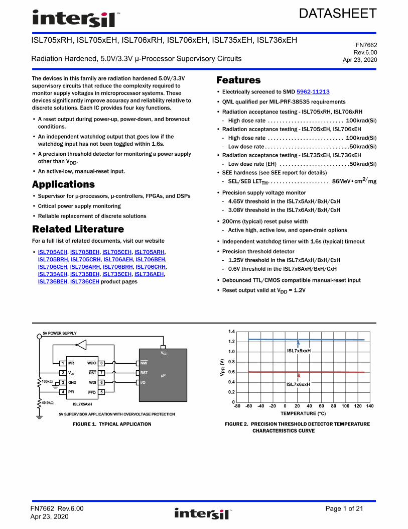
FIGURE 1. TYPICAL APPLICATION FIGURE 2. PRECISION THRESHOLD DETECTOR TEMPERATURE CHARACTERISTICS CURVE
1
2
3
4
8
7
6
5
MR
VDD
GND
PFI
WDO
RST
WDI
PFO
µP
165k
49.9k ISL7X5AxH
5V SUPERVISOR APPLICATION WITH OVERVOLTAGE PROTECTION
NMI
RST
I/O
VCC
5V POWER SUPPLY
0
0.2
0.4
0.6
0.8
1.0
1.2
1.4
-80 -60 -40 -20 0 20 40 60 80 100 120 140
TEMPERATURE (°C)
VP
FI (
V)
ISL7x5xxH
ISL7x6xxH
FN7662 Rev.6.00 Page 1 of 21Apr 23, 2020
ISL705xRH, ISL705xEH, ISL706xRH, ISL706xEH, ISL735xEH, ISL736xEH
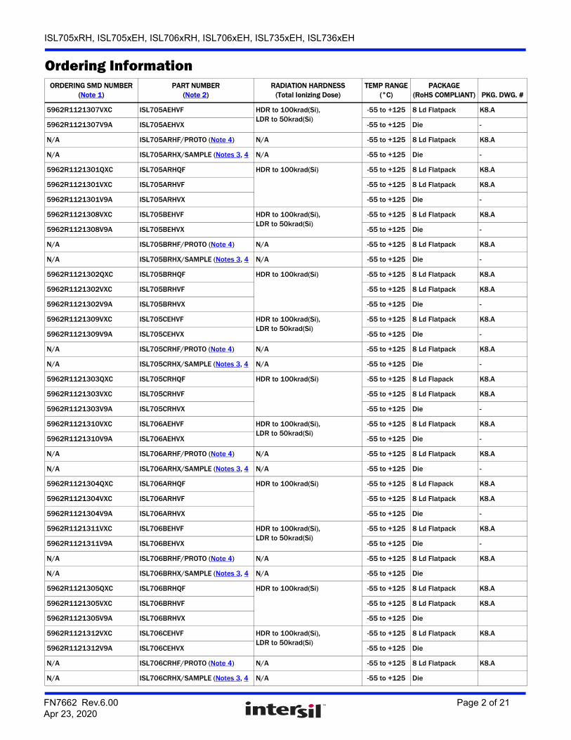
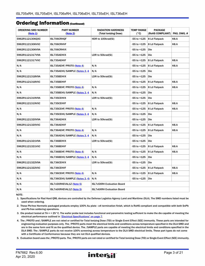
Ordering InformationORDERING SMD NUMBER
(Note 1)PART NUMBER
(Note 2)RADIATION HARDNESS
(Total Ionizing Dose)TEMP RANGE
(°C)PACKAGE
(RoHS COMPLIANT) PKG. DWG. #
5962R1121307VXC ISL705AEHVF HDR to 100krad(Si), LDR to 50krad(Si)
-55 to +125 8 Ld Flatpack K8.A
5962R1121307V9A ISL705AEHVX -55 to +125 Die -
N/A ISL705ARHF/PROTO (Note 4) N/A -55 to +125 8 Ld Flatpack K8.A
N/A ISL705ARHX/SAMPLE (Notes 3, 4 N/A -55 to +125 Die -
5962R1121301QXC ISL705ARHQF HDR to 100krad(Si) -55 to +125 8 Ld Flatpack K8.A
5962R1121301VXC ISL705ARHVF -55 to +125 8 Ld Flatpack K8.A
5962R1121301V9A ISL705ARHVX -55 to +125 Die -
5962R1121308VXC ISL705BEHVF HDR to 100krad(Si), LDR to 50krad(Si)
-55 to +125 8 Ld Flatpack K8.A
5962R1121308V9A ISL705BEHVX -55 to +125 Die -
N/A ISL705BRHF/PROTO (Note 4) N/A -55 to +125 8 Ld Flatpack K8.A
N/A ISL705BRHX/SAMPLE (Notes 3, 4 N/A -55 to +125 Die -
5962R1121302QXC ISL705BRHQF HDR to 100krad(Si) -55 to +125 8 Ld Flatpack K8.A
5962R1121302VXC ISL705BRHVF -55 to +125 8 Ld Flatpack K8.A
5962R1121302V9A ISL705BRHVX -55 to +125 Die -
5962R1121309VXC ISL705CEHVF HDR to 100krad(Si), LDR to 50krad(Si)
-55 to +125 8 Ld Flatpack K8.A
5962R1121309V9A ISL705CEHVX -55 to +125 Die -
N/A ISL705CRHF/PROTO (Note 4) N/A -55 to +125 8 Ld Flatpack K8.A
N/A ISL705CRHX/SAMPLE (Notes 3, 4 N/A -55 to +125 Die -
5962R1121303QXC ISL705CRHQF HDR to 100krad(Si) -55 to +125 8 Ld Flapack K8.A
5962R1121303VXC ISL705CRHVF -55 to +125 8 Ld Flatpack K8.A
5962R1121303V9A ISL705CRHVX -55 to +125 Die -
5962R1121310VXC ISL706AEHVF HDR to 100krad(Si), LDR to 50krad(Si)
-55 to +125 8 Ld Flatpack K8.A
5962R1121310V9A ISL706AEHVX -55 to +125 Die -
N/A ISL706ARHF/PROTO (Note 4) N/A -55 to +125 8 Ld Flatpack K8.A
N/A ISL706ARHX/SAMPLE (Notes 3, 4 N/A -55 to +125 Die -
5962R1121304QXC ISL706ARHQF HDR to 100krad(Si) -55 to +125 8 Ld Flapack K8.A
5962R1121304VXC ISL706ARHVF -55 to +125 8 Ld Flatpack K8.A
5962R1121304V9A ISL706ARHVX -55 to +125 Die -
5962R1121311VXC ISL706BEHVF HDR to 100krad(Si), LDR to 50krad(Si)
-55 to +125 8 Ld Flatpack K8.A
5962R1121311V9A ISL706BEHVX -55 to +125 Die -
N/A ISL706BRHF/PROTO (Note 4) N/A -55 to +125 8 Ld Flatpack K8.A
N/A ISL706BRHX/SAMPLE (Notes 3, 4 N/A -55 to +125 Die
5962R1121305QXC ISL706BRHQF HDR to 100krad(Si) -55 to +125 8 Ld Flatpack K8.A
5962R1121305VXC ISL706BRHVF -55 to +125 8 Ld Flatpack K8.A
5962R1121305V9A ISL706BRHVX -55 to +125 Die
5962R1121312VXC ISL706CEHVF HDR to 100krad(Si), LDR to 50krad(Si)
-55 to +125 8 Ld Flatpack K8.A
5962R1121312V9A ISL706CEHVX -55 to +125 Die
N/A ISL706CRHF/PROTO (Note 4) N/A -55 to +125 8 Ld Flatpack K8.A
N/A ISL706CRHX/SAMPLE (Notes 3, 4 N/A -55 to +125 Die
FN7662 Rev.6.00 Page 2 of 21Apr 23, 2020
ISL705xRH, ISL705xEH, ISL706xRH, ISL706xEH, ISL735xEH, ISL736xEH
5962R1121306QXC ISL706CRHQF HDR to 100krad(Si) -55 to +125 8 Ld Flatpack K8.A
5962R1121306VXC ISL706CRHVF -55 to +125 8 Ld Flatpack K8.A
5962R1121306V9A ISL706CRHVX -55 to +125 Die
5962R1121317V9A ISL735AEHVX LDR to 50krad(Si) -55 to +125 Die
5962R1121317VXC ISL735AEHVF -55 to +125 8 Ld Flatpack K8.A
N/A ISL735AEHF/PROTO (Note 4) N/A -55 to +125 8 Ld Flatpack K8.A
N/A ISL735AEHX/SAMPLE (Notes 3, 4 N/A -55 to +125 Die
5962R1121318V9A ISL735BEHVX LDR to 50krad(Si) -55 to +125 Die
5962R1121318VXC ISL735BEHVF -55 to +125 8 Ld Flatpack K8.A
N/A ISL735BEHF/PROTO (Note 4) N/A -55 to +125 8 Ld Flatpack K8.A
N/A ISL735BEHX/SAMPLE (Notes 3, 4 N/A -55 to +125 Die
5962R1121319V9A ISL735CEHVX LDR to 50krad(Si) -55 to +125 Die
5962R1121319VXC ISL735CEHVF -55 to +125 8 Ld Flatpack K8.A
N/A ISL735CEHF/PROTO (Note 4) N/A -55 to +125 8 Ld Flatpack K8.A
N/A ISL735CEHX/SAMPLE (Notes 3, 4 N/A -55 to +125 Die
5962R1121320V9A ISL736AEHVX LDR to 50krad(Si) -55 to +125 Die
5962R1121320VXC ISL736AEHVF -55 to +125 8 Ld Flatpack K8.A
N/A ISL736AEHF/PROTO (Note 4) N/A -55 to +125 8 Ld Flatpack K8.A
N/A ISL736AEHX/SAMPLE (Notes 3, 4 N/A -55 to +125 Die
5962R1121321V9A ISL736BEHVX LDR to 50krad(Si) -55 to +125 Die
5962R1121321VXC ISL736BEHVF -55 to +125 8 Ld Flatpack K8.A
N/A ISL736BEHF/PROTO (Note 4) N/A -55 to +125 8 Ld Flatpack K8.A
N/A ISL736BEHX/SAMPLE (Notes 3, 4 N/A -55 to +125 Die
5962R1121322V9A ISL736CEHVX LDR to 50krad(Si) -55 to +125 Die
5962R1121322VXC ISL736CEHVF -55 to +125 8 Ld Flatpack K8.A
N/A ISL736CEHF/PROTO (Note 4) N/A -55 to +125 8 Ld Flatpack K8.A
N/A ISL736CEHX/SAMPLE (Notes 3, 4) N/A -55 to +125 Die
N/A ISL7x5XRHEVAL1Z (Note 5) ISL7x5XRH Evaluation Board
N/A ISL7x6XRHEVAL1Z (Note 5) ISL7x6XRH Evaluation Board
NOTE:1. Specifications for Rad Hard QML devices are controlled by the Defense Logistics Agency Land and Maritime (DLA). The SMD numbers listed must be
used when ordering.
2. These Pb-free Hermetic packaged products employ 100% Au plate - e4 termination finish, which is RoHS compliant and compatible with both SnPb and Pb-free soldering operations.
3. Die product tested at TA = + 25°C. The wafer probe test includes functional and parametric testing sufficient to make the die capable of meeting the electrical performance outlined in “Electrical Specifications” on page 7.
4. The /PROTO and /SAMPLE are not rated or certified for Total Ionizing Dose (TID) or Single Event Effect (SEE) immunity. These parts are intended for engineering evaluation purposes only. The /PROTO parts meet the electrical limits and conditions across temperature specified in the DLA SMD and are in the same form and fit as the qualified device. The /SAMPLE parts are capable of meeting the electrical limits and conditions specified in the DLA SMD. The /SAMPLE parts do not receive 100% screening across temperature to the DLA SMD electrical limits. These part types do not come with a Certificate of Conformance because they are not DLA qualified devices.
5. Evaluation board uses the /PROTO parts. The /PROTO parts are not rated or certified for Total Ionizing Dose (TID) or Single Event Effect (SEE) immunity.
Ordering Information (Continued)
ORDERING SMD NUMBER(Note 1)
PART NUMBER(Note 2)
RADIATION HARDNESS(Total Ionizing Dose)
TEMP RANGE(°C)
PACKAGE(RoHS COMPLIANT) PKG. DWG. #
FN7662 Rev.6.00 Page 3 of 21Apr 23, 2020
ISL705xRH, ISL705xEH, ISL706xRH, ISL706xEH, ISL735xEH, ISL736xEH
Pin ConfigurationsISL7X5AxH, ISL7X6AxH
(8 LD FLATPACK)TOP VIEW
ISL7X5BxH, ISL7X6BxH(8 LD FLATPACK)
TOP VIEW
ISL7X5CxH, ISL7X6CxH(8 LD FLATPACK)
TOP VIEW
1
2
3
4
8
7
6
5
VDD
GND
PFI
WDO
RST
WDI
PFO
MR 1
2
3
4
8
7
6
5
VDD
GND
PFI
WDO
RST
WDI
PFO
MR 1
2
3
4
8
7
6
5
VDD
GND
PFI
WDO
RST_OD
WDI
PFO
MR
Pin DescriptionsISL7x5AxH ISL7x6AxH
ISL7x5BxH ISL7x6BxH
ISL7x5CxH ISL7x6CxH
PINNAME DESCRIPTION
1 1 1 MR Manual Reset. MR is an active-low, debounced, TTL/CMOS compatible input that can be used to trigger a reset pulse.
2 2 2 VDD Power Supply. VDD is a supply voltage input that provides power to all internal circuitry. This input is also monitored and used to trigger a reset pulse. Reset is guaranteed operable after VDD rises above 1.2V.
3 3 3 GND Ground. GND is a supply voltage return for all internal circuitry. This return establishes the reference level for voltage detection and should be connected to signal ground.
4 4 4 PFI Power Fail Input. PFI is an input to a threshold detector, which can be used to monitor another supply voltage level. The threshold of the detector (VPFI) is 1.25V in the ISL7x5AxH/BxH/CxH and 0.6V in the ISL7x6AxH/BxH/CxH.
5 5 5 PFO Power Fail Output. PFO is an active-low, push-pull output of a threshold detector that indicates the voltage at the PFI pin is less than VPFI.
6 6 6 WDI Watchdog Input. WDI is a tri-state input that monitors microprocessor activity. If the microprocessor does not toggle WDI within 1.6s and WDI is not tri-stated, WDO goes low. As long as reset is asserted or WDI is tri-stated, the watchdog timer will stay cleared and will not count. As soon as reset is released and WDI is driven high or low, the timer will start counting. Floating WDI or connecting WDI to a high impedance tri-state buffer disables the watchdog feature.
7 - - RST Reset. RST is an active-low, push-pull output that is guaranteed to be low after VDD reaches 1.2V. As VDD rises, RST stays low. When VDD rises above a 4.65V (ISL7x5AxH/BxH/CxH) or 3.08V (ISL7x6AxH/BxH/CxH) reset threshold, an internal timer releases RST after about 200ms. RST pulses low whenever VDD goes below the reset threshold. If a brownout condition occurs in the middle of a previously initiated reset pulse, the pulse will continue for at least 140ms. On power-down, after VDD falls below the reset threshold, RST goes low and is guaranteed low until VDD drops below 1.2V.
- 7 - RST Reset. RST is an active-high, push-pull output. RST is the inverse of RST.
- - 7 RST_OD Reset. RST_OD is an active-low, open-drain output that goes low when reset is asserted. This pin can be pulled up to VDD with a resistor consistent with the sink and leakage current specifications of the output. Behavior is otherwise identical to the RST pin.
8 8 8 WDO Watchdog Output. WDO is an active-low, push-pull output that goes low if the microprocessor does not toggle WDI within 1.6s and WDI is not tri-stated. WDO is usually connected to the non-maskable interrupt input of a microprocessor. When VDD drops below the reset threshold, WDO will go low whether or not the watchdog timer has timed out. Reset is simultaneously asserted, thus preventing an interrupt. Since floating WDI disables the internal timer, WDO goes low only when VDD drops below the reset threshold, thus functioning as a low line output.
FN7662 Rev.6.00 Page 4 of 21Apr 23, 2020
ISL705xRH, ISL705xEH, ISL706xRH, ISL706xEH, ISL735xEH, ISL736xEH
D
Functional Block Diagrams
FIGURE 3A. ISL7x5AxH, ISL7x6AxH FIGURE 3B. ISL7x5BxH, ISL7x6BxH FIGURE 3C. ISL7x5CxH, ISL7x6CxH
FIGURE 3. FUNCTIONAL BLOCK DIAGRAMS
+ VREF
VDD
POR
GND
WDT
VREF
PFI
WDI
PB
WDO
PF PFO
MR
RST
-
+-
VREF
VDD
POR
GND
WDT
VREF
PFI
WDI
PB
WDO
PF PFO
MR
RST
+-
+- VREF
VDD
POR
GND
WDT
VREF
PFI
WDI
PB
WDO
PF PFO
MR
RST_O
+-
+-
Timing Diagrams
FIGURE 4. RST, RST, MR TIMING DIAGRAM
VDD
MR
RST
tRST
VRST
1.2V
tRSTtRST
>tMR
RST
<tMD
WDI
FN7662 Rev.6.00 Page 5 of 21Apr 23, 2020
ISL705xRH, ISL705xEH, ISL706xRH, ISL706xEH, ISL735xEH, ISL736xEH
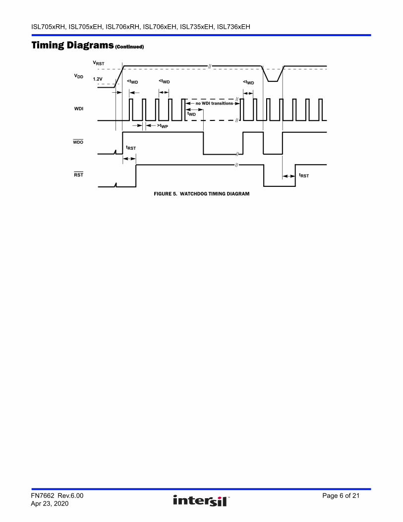
FIGURE 5. WATCHDOG TIMING DIAGRAM
Timing Diagrams (Continued)
VRST
1.2V
tWD
>tWP
<tWD<tWD <tWD
tRST
tRST
RST
WDO
WDI
VDD
no WDI transitions
FN7662 Rev.6.00 Page 6 of 21Apr 23, 2020
ISL705xRH, ISL705xEH, ISL706xRH, ISL706xEH, ISL735xEH, ISL736xEH
Absolute Maximum Ratings Thermal InformationSupply Voltage Range . . . . . . . . . . . . . . . . . . . . . . . . . . . . . . . . -0.3V to 6.5VVoltage on All Other Inputs . . . . . . . . . . . . . . . . . . . . . . . -0.3V to VDD + 0.3VESD Rating
Human Body Model (Tested per MIL-PRF-883 3015.7). . . . . . . . . .3.0kVMachine Model (Tested per JESD22-A115C) . . . . . . . . . . . . . . . . . . 300VCharged Device Model (Tested per JESD22-C110D) . . . . . . . . . . . .1.0kV
Latch-Up (Tested per JESD-78C) . . . . . . . . . . . . . . . . . . . . . . Class 2, Level A
Thermal Resistance (Typical) JA (°C/W) JC (°C/W)8 Ld Flatpack Package (Notes 6, 7). . . . . . 140 15
Maximum Junction Temperature . . . . . . . . . . . . . . . . . . . . . . . . . . . .+175°CStorage Temperature Range. . . . . . . . . . . . . . . . . . . . . . . .-65°C to +150°C
Recommended Operating ConditionsTemperature . . . . . . . . . . . . . . . . . . . . . . . . . . . . . . . . . . . . .-55°C to +125°CSupply Voltage
ISL7x5AxH/BxH/CxH . . . . . . . . . . . . . . . . . . . . . . . . . . . . . . . 4.75V to 5.5VISL7x6AxH/BxH/CxH . . . . . . . . . . . . . . . . . . . . . . . . . . . . . . . 3.15V to 3.6V
CAUTION: Do not operate at or near the maximum ratings listed for extended periods of time. Exposure to such conditions may adversely impact productreliability and result in failures not covered by warranty.
NOTES:
6. JA is measured with the component mounted on a low-effective thermal conductivity test board in free air. See Tech Brief TB379 for details.
7. For JC, the “case temp” location is the center of the package underside.
Electrical Specifications Unless otherwise specified VDD = 4.75V to 5.5V for the ISL7x5AxH/BxH/CxH, VDD = 3.15V to 3.6V for the ISL7x6AxH/BxH/CxH, TA = -55°C to +125°C. Boldface limits apply across the operating temperature range, -55°C to +125°C; over a total ionizing dose of 100krad(Si) with exposure at a high dose rate of 50 - 300krad(Si)/s; and over a total ionizing dose of 50krad(Si) with exposure at a low dose rate of <10mrad(Si)/s.
PARAMETER SYMBOL TEST CONDITIONSMIN
(Note 8)TYP
(Note 9)MAX
(Note 8) UNIT
POWER SUPPLY SECTION
Operating Supply Voltage (Note 10) VDD ISL7x5AxH/BxH/CxH 1.2 5.0 5.5 V
ISL7x6AxH/BxH/CxH 1.2 3.3 3.6 V
Operating Supply Current IDD ISL7x5AxH/BxH/CxH 530 µA
ISL7x6AxH/BxH/CxH 400 µA
RESET SECTION
Reset Threshold Voltage VRST ISL7x5AxH/BxH/CxH 4.50 4.65 4.75 V
ISL7x6AxH/BxH/CxH 3.00 3.08 3.15 V
Reset Threshold Voltage Hysteresis VHYS ISL7x5AxH/BxH/CxH 20 40 mV
ISL7x6AxH/BxH/CxH 20 30 mV
Reset Pulse Width tRST 140 200 280 ms
Reset Output Voltage VOUT ISL7x5AxH/BxH, ISOURCE = 800µA VDD - 1.5 V
ISL7x5AxH/BxH/CxH, ISINK = 3.2mA 0.4 V
ISL7x6AxH/BxH, ISOURCE = 500µA 0.8 x VDD V
ISL7x6AxH/BxH/CxH, ISINK = 1.2mA 0.3 V
ISL7xXAxH/CxH, VDD = 1.2V, ISINK = 100µA 0.3 V
ISL7xXBxH, VDD = 1.2V, ISOURCE = 4µA 0.9 V
Reset Output Leakage Current ILEAK ISL7x5CxH, VOUT = VDD 1 µA
ISL7x6CxH, VOUT = VDD 1 µA
FN7662 Rev.6.00 Page 7 of 21Apr 23, 2020
ISL705xRH, ISL705xEH, ISL706xRH, ISL706xEH, ISL735xEH, ISL736xEH
WATCHDOG SECTION
Watchdog Time-Out Period tWD 1.00 1.60 2.25 s
Watchdog Input (WDI) Pulse Width tWP ISL7x5AxH/BxH/CxH, VIL = 0.4V, VIH = 0.8 x VDD 50 ns
ISL7x6AxH/BxH/CxH, VIL = 0.4V, VIH = 0.8 x VDD 100 ns
Watchdog Input (WDI) Threshold Voltage VIL ISL7x5AxH/BxH/CxH 0.8 V
VIH ISL7x5AxH/BxH/CxH 3.5 V
VIL ISL7x6AxH/BxH/CxH 0.6 V
VIH ISL7x6AxH/BxH/CxH 0.7 x VDD V
Watchdog Input (WDI) Current IWDI ISL7x5AxH/BxH/CxH, WDI = VDD 100 µA
ISL7x5AxH/BxH/CxH, WDI = 0V -100 µA
ISL7x6AxH/BxH/CxH, WDI = VDD 5 µA
ISL7x6AxH/BxH/CxH, WDI = 0V -5 µA
Watchdog Output (WDO) Voltage VWDO ISL7x5AxH/BxH/CxH, ISOURCE = 800µA VDD - 1.5 V
ISL7x5AxH/BxH/CxH, ISINK = 1.2mA 0.4 V
ISL7x6AxH/BxH/CxH, ISOURCE = 500µA 0.8 x VDD V
ISL7x6AxH/BxH/CxH, ISINK = 500µA 0.3 V
MANUAL RESET SECTION
Manual Reset (MR) Pull-Up Current IMR ISL7x5AxH/BxH/CxH, MR = 0V -500 -100 µA
ISL7x6AxH/BxH/CxH, MR = 0V -250 -25 µA
Manual Reset (MR) Pulse Width tMR ISL7x5AxH/BxH/CxH 150 ns
ISL7x6AxH/BxH/CxH 150 ns
Manual Reset (MR) Input Threshold Voltage VIL ISL7x5AxH/BxH/CxH 0.8 V
VIH 2.0 V
VIL ISL7x6AxH/BxH/CxH 0.6 V
VIH 0.7 x VDD V
Manual Reset (MR) to Reset Out Delay tMD ISL7x5AxH/BxH/CxH 100 ns
ISL7x6AxH/BxH/CxH 100 ns
THRESHOLD DETECTOR SECTION
Power Fail Input (PFI) Input Threshold Voltage
VPFI ISL7x5AxH/BxH/CxH 1.20 1.25 1.30 V
ISL7x6AxH/BxH/CxH 0.576 0.600 0.624 V
Power Fail Input (PFI) Input Current IPFI -10 10 nA
Power Fail Output (PFO) Output Voltage VPFO ISL7x5AxH/BxH/CxH, ISOURCE = 800µA VDD - 1.5 V
ISL7x5AxH/BxH/CxH, ISINK = 3.2mA 0.4 V
ISL7x6AxH/BxH/CxH, ISOURCE = 500µA 0.8 x VDD V
ISL7x6ARH/BRH/CRH, ISINK = 1.2mA 0.3 V
PFI Rising Threshold Crossing to PFO Delay
tRPFI ISL7x5AxH/BxH/CxH 7 15 µs
ISL7x6AxH/BxH/CxH 11 20 µs
Electrical Specifications Unless otherwise specified VDD = 4.75V to 5.5V for the ISL7x5AxH/BxH/CxH, VDD = 3.15V to 3.6V for the ISL7x6AxH/BxH/CxH, TA = -55°C to +125°C. Boldface limits apply across the operating temperature range, -55°C to +125°C; over a total ionizing dose of 100krad(Si) with exposure at a high dose rate of 50 - 300krad(Si)/s; and over a total ionizing dose of 50krad(Si) with exposure at a low dose rate of <10mrad(Si)/s. (Continued)
PARAMETER SYMBOL TEST CONDITIONSMIN
(Note 8)TYP
(Note 9)MAX
(Note 8) UNIT
FN7662 Rev.6.00 Page 8 of 21Apr 23, 2020
ISL705xRH, ISL705xEH, ISL706xRH, ISL706xEH, ISL735xEH, ISL736xEH
PFI Falling Threshold Crossing to PFO Delay
tFPFI ISL7x5AxH/BxH/CxH 20 35 µs
ISL7x6AxH/BxH/CxH 25 40 µs
NOTES:
8. Compliance to datasheet limits is assured by one or more methods: production test, characterization, and/or design.
9. Typical values shown reflect TA = TJ = +25°C operation and are not guaranteed.
10. Reset is the only parameter operable within 1.2V and the minimum recommended operating supply voltage.
Electrical Specifications Unless otherwise specified VDD = 4.75V to 5.5V for the ISL7x5AxH/BxH/CxH, VDD = 3.15V to 3.6V for the ISL7x6AxH/BxH/CxH, TA = -55°C to +125°C. Boldface limits apply across the operating temperature range, -55°C to +125°C; over a total ionizing dose of 100krad(Si) with exposure at a high dose rate of 50 - 300krad(Si)/s; and over a total ionizing dose of 50krad(Si) with exposure at a low dose rate of <10mrad(Si)/s. (Continued)
PARAMETER SYMBOL TEST CONDITIONSMIN
(Note 8)TYP
(Note 9)MAX
(Note 8) UNIT
FN7662 Rev.6.00 Page 9 of 21Apr 23, 2020
ISL705xRH, ISL705xEH, ISL706xRH, ISL706xEH, ISL735xEH, ISL736xEH
Typical Performance Curves
FIGURE 6. IDD vs TEMPERATURE FIGURE 7. VRST vs TEMPERATURE
FIGURE 8. VPFI vs TEMPERATURE FIGURE 9. ISL7x5xRH RESET and RESET ASSERTION
FIGURE 10. ISL7x5xRH RESET AND RESET DEASSERTION FIGURE 11. ISL7x6xRH RESET AND RESET ASSERTION
200
250
300
350
400
450
500
550
-80 -60 -40 -20 0 20 40 60 80 100 120 140
TEMPERATURE (°C)
I DD
(µ
A)
ISL7x5xRH
ISL7x6xRH
2.0
2.5
3.0
3.5
4.0
4.5
5.0
-80 -60 -40 -20 0 20 40 60 80 100 120 140
VR
ST (
V)
TEMPERATURE (°C)
ISL7x5xRH
ISL7x6xRH
0
0.2
0.4
0.6
0.8
1.0
1.2
1.4
-80 -60 -40 -20 0 20 40 60 80 100 120 140
TEMPERATURE (°C)
VP
FI (
V)
ISL7x5xRH
ISL7x6xRH
VDD
RST
RST
VDD
RST
RST
VDD
RST
RST
FN7662 Rev.6.00 Page 10 of 21Apr 23, 2020
ISL705xRH, ISL705xEH, ISL706xRH, ISL706xEH, ISL735xEH, ISL736xEH
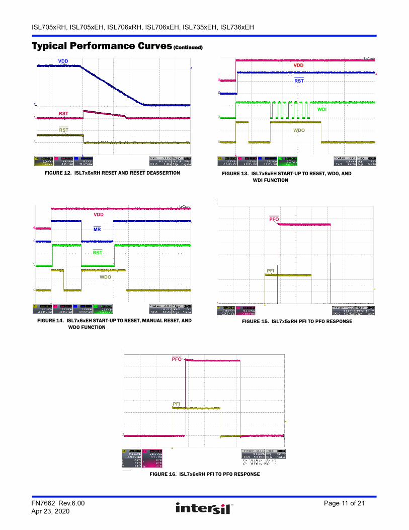
FIGURE 12. ISL7x6xRH RESET AND RESET DEASSERTION FIGURE 13. ISL7x6xEH START-UP TO RESET, WDO, AND WDI FUNCTION
FIGURE 14. ISL7x6xEH START-UP TO RESET, MANUAL RESET, AND WDO FUNCTION
FIGURE 15. ISL7x5xRH PFI TO PFO RESPONSE
FIGURE 16. ISL7x6xRH PFI TO PFO RESPONSE
Typical Performance Curves (Continued)
VDD
RST
RST
VDD
RST
WDI
WDO
VDD
WDO
MR
RST
PFO
PFI
PFI
PFO
FN7662 Rev.6.00 Page 11 of 21Apr 23, 2020
ISL705xRH, ISL705xEH, ISL706xRH, ISL706xEH, ISL735xEH, ISL736xEH
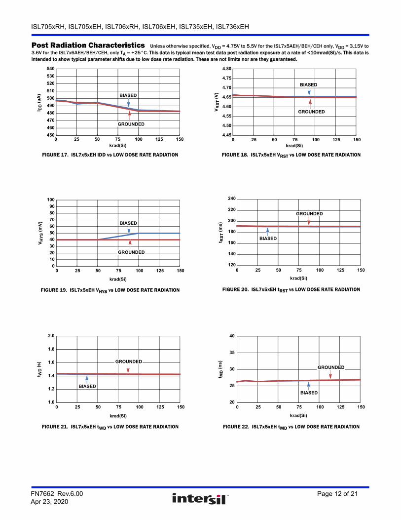
Post Radiation Characteristics Unless otherwise specified, VDD = 4.75V to 5.5V for the ISL7x5AEH/BEH/CEH only, VDD = 3.15V to 3.6V for the ISL7x6AEH/BEH/CEH, only TA = +25°C. This data is typical mean test data post radiation exposure at a rate of <10mrad(Si)/s. This data is intended to show typical parameter shifts due to low dose rate radiation. These are not limits nor are they guaranteed.
FIGURE 17. ISL7x5xEH IDD vs LOW DOSE RATE RADIATION FIGURE 18. ISL7x5xEH VRST vs LOW DOSE RATE RADIATION
FIGURE 19. ISL7x5xEH VHYS vs LOW DOSE RATE RADIATION FIGURE 20. ISL7x5xEH tRST vs LOW DOSE RATE RADIATION
FIGURE 21. ISL7x5xEH tWD vs LOW DOSE RATE RADIATION FIGURE 22. ISL7x5xEH tMD vs LOW DOSE RATE RADIATION
krad(Si)
I DD
(µ
A)
450
460
470
480
490
500
510
520
530
540
0 25 50 75 100 125 150
BIASED
GROUNDED
VR
ST (
V)
krad(Si)
4.45
4.50
4.55
4.60
4.65
4.70
4.75
4.80
0 25 50 75 100 125 150
BIASED
GROUNDED
0
10
20
30
40
50
60
70
80
90
100
0 25 50 75 100 125 150
krad(Si)
VH
YS
(m
V) BIASED
GROUNDED
120
140
160
180
200
220
240
0 25 50 75 100 125 150
t RS
T (
ms
)
krad(Si)
BIASED
GROUNDED
1.0
1.2
1.4
1.6
1.8
2.0
0 25 50 75 100 125 150
t WD
(s)
krad(Si)
BIASED
GROUNDED
20
25
30
35
40
0 25 50 75 100 125 150
t MD
(n
s)
krad(Si)
BIASED
GROUNDED
FN7662 Rev.6.00 Page 12 of 21Apr 23, 2020
ISL705xRH, ISL705xEH, ISL706xRH, ISL706xEH, ISL735xEH, ISL736xEH
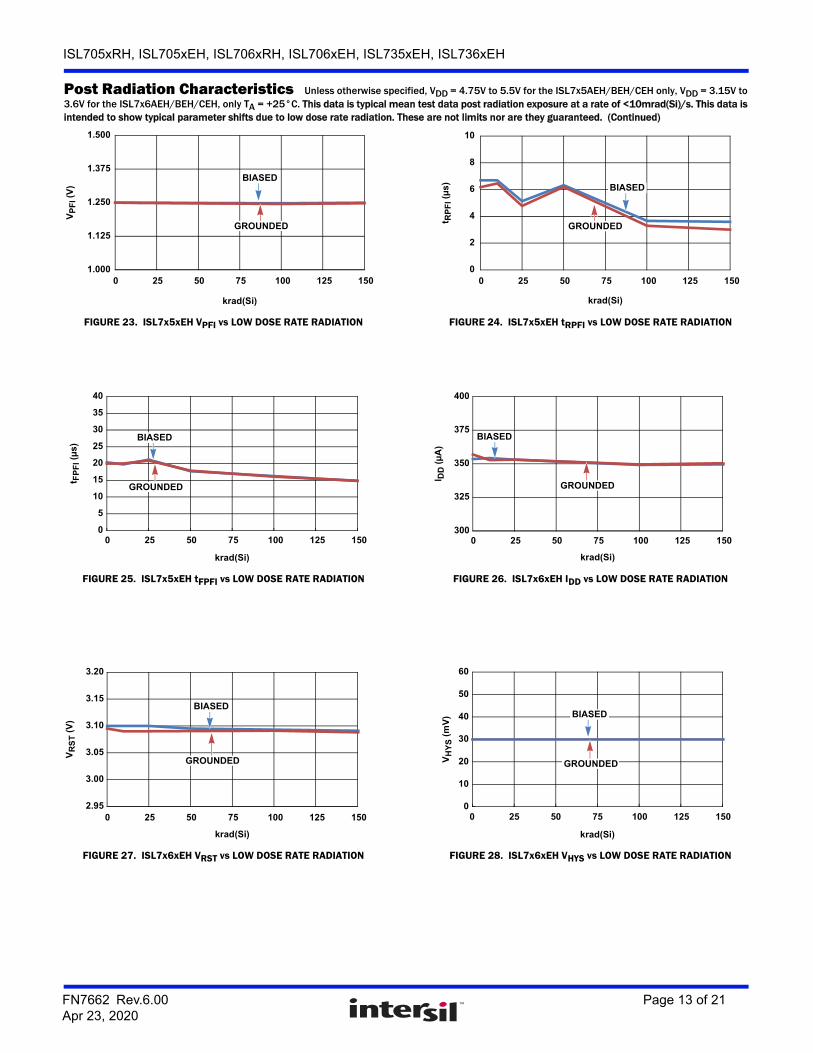
FIGURE 23. ISL7x5xEH VPFI vs LOW DOSE RATE RADIATION FIGURE 24. ISL7x5xEH tRPFI vs LOW DOSE RATE RADIATION
FIGURE 25. ISL7x5xEH tFPFI vs LOW DOSE RATE RADIATION FIGURE 26. ISL7x6xEH IDD vs LOW DOSE RATE RADIATION
FIGURE 27. ISL7x6xEH VRST vs LOW DOSE RATE RADIATION FIGURE 28. ISL7x6xEH VHYS vs LOW DOSE RATE RADIATION
Post Radiation Characteristics Unless otherwise specified, VDD = 4.75V to 5.5V for the ISL7x5AEH/BEH/CEH only, VDD = 3.15V to 3.6V for the ISL7x6AEH/BEH/CEH, only TA = +25°C. This data is typical mean test data post radiation exposure at a rate of <10mrad(Si)/s. This data is intended to show typical parameter shifts due to low dose rate radiation. These are not limits nor are they guaranteed. (Continued)
1.000
1.125
1.250
1.375
1.500
0 25 50 75 100 125 150
VP
FI (V
)
krad(Si)
BIASED
GROUNDED
0
2
4
6
8
10
0 25 50 75 100 125 150
t RP
FI (
µs
)
krad(Si)
BIASED
GROUNDED
0
5
10
15
20
25
30
35
40
0 25 50 75 100 125 150
t FP
FI (
µs
)
krad(Si)
BIASED
GROUNDED
300
325
350
375
400
0 25 50 75 100 125 150
krad(Si)
I DD
(µ
A)
BIASED
GROUNDED
2.95
3.00
3.05
3.10
3.15
3.20
0 25 50 75 100 125 150
VR
ST (
V)
krad(Si)
BIASED
GROUNDED
0
10
20
30
40
50
60
0 25 50 75 100 125 150
krad(Si)
VH
YS
(m
V) BIASED
GROUNDED
FN7662 Rev.6.00 Page 13 of 21Apr 23, 2020
ISL705xRH, ISL705xEH, ISL706xRH, ISL706xEH, ISL735xEH, ISL736xEH
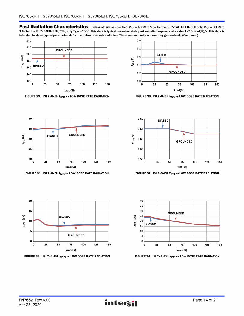
FIGURE 29. ISL7x6xEH tRST vs LOW DOSE RATE RADIATION FIGURE 30. ISL7x6xEH tWD vs LOW DOSE RATE RADIATION
FIGURE 31. ISL7x6xEH tMD vs LOW DOSE RATE RADIATION FIGURE 32. ISL7x6xEH VPFI vs LOW DOSE RATE RADIATION
FIGURE 33. ISL7x6xEH tRPFI vs LOW DOSE RATE RADIATION FIGURE 34. ISL7x6xEH tFPFI vs LOW DOSE RATE RADIATION
Post Radiation Characteristics Unless otherwise specified, VDD = 4.75V to 5.5V for the ISL7x5AEH/BEH/CEH only, VDD = 3.15V to 3.6V for the ISL7x6AEH/BEH/CEH, only TA = +25°C. This data is typical mean test data post radiation exposure at a rate of <10mrad(Si)/s. This data is intended to show typical parameter shifts due to low dose rate radiation. These are not limits nor are they guaranteed. (Continued)
120
140
160
180
200
220
240
0 25 50 75 100 125 150
t RS
T (
ms)
krad(Si)
BIASED
GROUNDED
1.0
1.2
1.4
1.6
1.8
2.0
0 25 50 75 100 125 150
t WD
(s
)
krad(Si)
BIASED
GROUNDED
20
25
30
35
40
0 25 50 75 100 125 150
t MD
(n
s)
krad(Si)
BIASED GROUNDED
0.58
0.59
0.60
0.61
0.62
0 25 50 75 100 125 150
VP
FI (
V)
krad(Si)
BIASED
GROUNDED
t RP
FI (
µs
)
krad(Si)
0
5
10
15
20
0 25 50 75 100 125 150
BIASED
GROUNDED
0
5
10
15
20
25
30
35
40
0 25 50 75 100 125 150
t FP
FI (
µs
)
krad(Si)
BIASED
GROUNDED
FN7662 Rev.6.00 Page 14 of 21Apr 23, 2020
ISL705xRH, ISL705xEH, ISL706xRH, ISL706xEH, ISL735xEH, ISL736xEH
Functional OverviewThe ISL7x5xxH and ISL7x6xxH provide the functions needed for monitoring critical voltages in high reliability applications such as microprocessor systems. Functions of the these supervisors include power-on reset control, supply voltage supervisions, power-fail detection, manual-reset assertion, and a watchdog timer. The integration of these functions along with their high threshold accuracy, low power consumption, and radiation tolerance make these devices ideal for critical supply monitoring.
The family of devices are differentiated only be the radiation assurance levels that each one is qualified to. See the Ordering Information table on page 2 for details on the radiation assurance levels each device obtains.
Reset OutputReset control has long been a critical aspect of embedded control design. Microprocessors require a reset signal during power-up to ensure that the system environment is stable before initialization.
The reset signal provides several benefits:
• It prevents the system microprocessor from starting to operate with insufficient voltage.
• It prevents the processor from operating before stabilization of the oscillator.
• It ensures that the monitored device is held out of operation until internal registers are initialized.
• It allows time for an FPGA to perform its self configuration before initialization of the circuit.
On power-up, after VDD reaches 1.2V, RST is guaranteed logic low. As VDD rises, RST stays low. When VDD rises above the reset threshold (VRST), an internal timer releases RST after 200ms (typical). RST pulses low whenever VDD degrades to below VRST (see Figure 4). If a brownout condition occurs in the middle of a previously initiated reset pulse, the pulse is lengthened 200ms (typical).
On power-down, after VDD falls below the reset threshold, RST stays low and is guaranteed to be low until VDD drops below 1.2V.
The ISL7x5BxH and ISL7x6BxH active-high RST output is simply the complement of the RST output and is guaranteed to be valid with VDD down to 1.2V. The ISL7x5CxH and ISL7x6CxH active-low open-drain reset output is functionally identical to RST.
Power Failure MonitorBesides monitoring VDD for reset control, these devices have a Power Failure Monitor feature that supervises an additional critical voltage on the Power-Fail Input (PFI) pin. For example, the PFI pin could be used to provide an early power-fail warning, overvoltage detection, or monitor a power supply other than VDD. PFO goes low whenever PFI is less than VPFI.
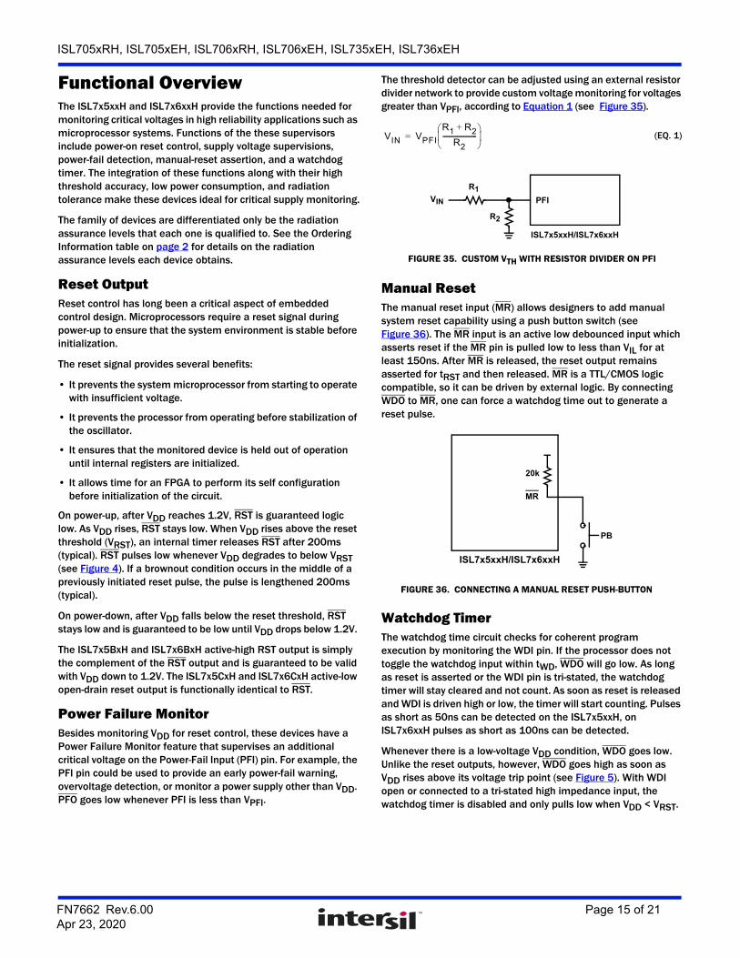
The threshold detector can be adjusted using an external resistor divider network to provide custom voltage monitoring for voltages greater than VPFI, according to Equation 1 (see Figure 35).
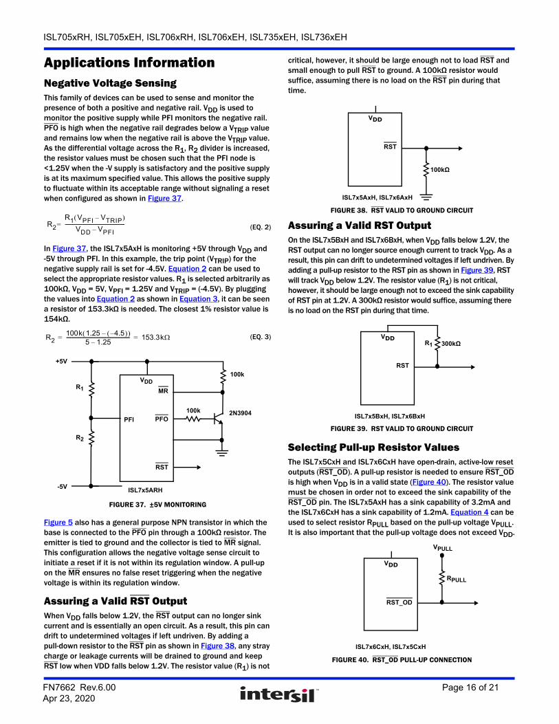
Manual ResetThe manual reset input (MR) allows designers to add manual system reset capability using a push button switch (see Figure 36). The MR input is an active low debounced input which asserts reset if the MR pin is pulled low to less than VIL for at least 150ns. After MR is released, the reset output remains asserted for tRST and then released. MR is a TTL/CMOS logic compatible, so it can be driven by external logic. By connecting WDO to MR, one can force a watchdog time out to generate a reset pulse.
Watchdog TimerThe watchdog time circuit checks for coherent program execution by monitoring the WDI pin. If the processor does not toggle the watchdog input within tWD, WDO will go low. As long as reset is asserted or the WDI pin is tri-stated, the watchdog timer will stay cleared and not count. As soon as reset is released and WDI is driven high or low, the timer will start counting. Pulses as short as 50ns can be detected on the ISL7x5xxH, on ISL7x6xxH pulses as short as 100ns can be detected.
Whenever there is a low-voltage VDD condition, WDO goes low. Unlike the reset outputs, however, WDO goes high as soon as VDD rises above its voltage trip point (see Figure 5). With WDI open or connected to a tri-stated high impedance input, the watchdog timer is disabled and only pulls low when VDD < VRST.
VIN VPFI
R1 R2+
R2---------------------
= (EQ. 1)
FIGURE 35. CUSTOM VTH WITH RESISTOR DIVIDER ON PFI
VIN
R1
R2
PFI
ISL7x5xxH/ISL7x6xxH
MR
PB
20k
FIGURE 36. CONNECTING A MANUAL RESET PUSH-BUTTON
ISL7x5xxH/ISL7x6xxH
FN7662 Rev.6.00 Page 15 of 21Apr 23, 2020
ISL705xRH, ISL705xEH, ISL706xRH, ISL706xEH, ISL735xEH, ISL736xEH
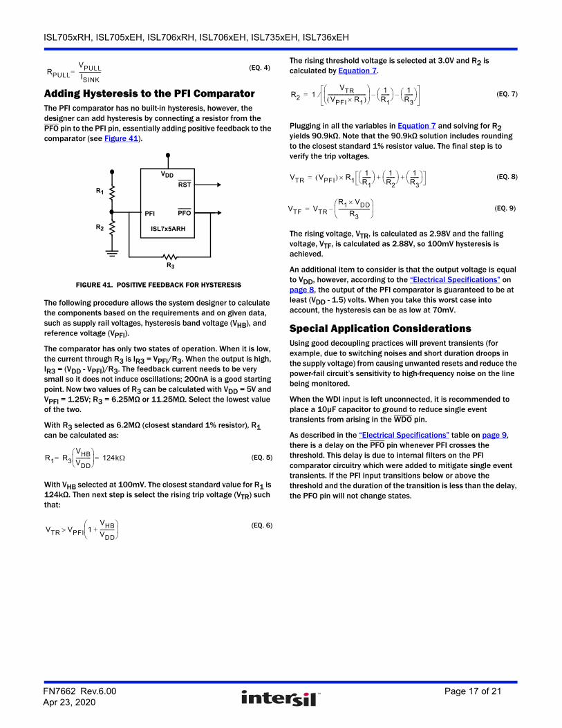
Applications InformationNegative Voltage SensingThis family of devices can be used to sense and monitor the presence of both a positive and negative rail. VDD is used to monitor the positive supply while PFI monitors the negative rail. PFO is high when the negative rail degrades below a VTRIP value and remains low when the negative rail is above the VTRIP value. As the differential voltage across the R1, R2 divider is increased, the resistor values must be chosen such that the PFI node is <1.25V when the -V supply is satisfactory and the positive supply is at its maximum specified value. This allows the positive supply to fluctuate within its acceptable range without signaling a reset when configured as shown in Figure 37.
In Figure 37, the ISL7x5AxH is monitoring +5V through VDD and -5V through PFI. In this example, the trip point (VTRIP) for the negative supply rail is set for -4.5V. Equation 2 can be used to select the appropriate resistor values. R1 is selected arbitrarily as 100kΩ, VDD = 5V, VPFI = 1.25V and VTRIP = (-4.5V). By plugging the values into Equation 2 as shown in Equation 3, it can be seen a resistor of 153.3kΩ is needed. The closest 1% resistor value is 154kΩ.
Figure 5 also has a general purpose NPN transistor in which the base is connected to the PFO pin through a 100kΩ resistor. The emitter is tied to ground and the collector is tied to MR signal. This configuration allows the negative voltage sense circuit to initiate a reset if it is not within its regulation window. A pull-up on the MR ensures no false reset triggering when the negative voltage is within its regulation window.
Assuring a Valid RST OutputWhen VDD falls below 1.2V, the RST output can no longer sink current and is essentially an open circuit. As a result, this pin can drift to undetermined voltages if left undriven. By adding a pull-down resistor to the RST pin as shown in Figure 38, any stray charge or leakage currents will be drained to ground and keep RST low when VDD falls below 1.2V. The resistor value (R1) is not
critical, however, it should be large enough not to load RST and small enough to pull RST to ground. A 100kΩ resistor would suffice, assuming there is no load on the RST pin during that time.
Assuring a Valid RST OutputOn the ISL7x5BxH and ISL7x6BxH, when VDD falls below 1.2V, the RST output can no longer source enough current to track VDD. As a result, this pin can drift to undetermined voltages if left undriven. By adding a pull-up resistor to the RST pin as shown in Figure 39, RST will track VDD below 1.2V. The resistor value (R1) is not critical, however, it should be large enough not to exceed the sink capability of RST pin at 1.2V. A 300kΩ resistor would suffice, assuming there is no load on the RST pin during that time.
Selecting Pull-up Resistor ValuesThe ISL7x5CxH and ISL7x6CxH have open-drain, active-low reset outputs (RST_OD). A pull-up resistor is needed to ensure RST_OD is high when VDD is in a valid state (Figure 40). The resistor value must be chosen in order not to exceed the sink capability of the RST_OD pin. The ISL7x5AxH has a sink capability of 3.2mA and the ISL7x6CxH has a sink capability of 1.2mA. Equation 4 can be used to select resistor RPULL based on the pull-up voltage VPULL. It is also important that the pull-up voltage does not exceed VDD.
FIGURE 37. ±5V MONITORING
R2
R1 VPFI VTRIP–
VDD VPFI–-------------------------------------------------= (EQ. 2)
R2 100k 1.25 4.5– –
5 1.25–---------------------------------------------------- 153.3k== (EQ. 3)
+5V
ISL7x5ARH-5V
100k
100k 2N3904
MR
RST
PFOPFI
R1
R2
VDD
FIGURE 38. RST VALID TO GROUND CIRCUIT
FIGURE 39. RST VALID TO GROUND CIRCUIT
FIGURE 40. RST_OD PULL-UP CONNECTION
ISL7x5AxH, ISL7x6AxH
100kΩ
RST
VDD
ISL7x5BxH, ISL7x6BxH
300kΩ
RST
VDDR1
ISL7x6CxH, ISL7x5CxH
RPULL
RST_OD
VDD
VPULL
FN7662 Rev.6.00 Page 16 of 21Apr 23, 2020
ISL705xRH, ISL705xEH, ISL706xRH, ISL706xEH, ISL735xEH, ISL736xEH
Adding Hysteresis to the PFI ComparatorThe PFI comparator has no built-in hysteresis, however, the designer can add hysteresis by connecting a resistor from the PFO pin to the PFI pin, essentially adding positive feedback to the comparator (see Figure 41).
The following procedure allows the system designer to calculate the components based on the requirements and on given data, such as supply rail voltages, hysteresis band voltage (VHB), and reference voltage (VPFI).
The comparator has only two states of operation. When it is low, the current through R3 is IR3 = VPFI/R3. When the output is high, IR3 = (VDD - VPFI)/R3. The feedback current needs to be very small so it does not induce oscillations; 200nA is a good starting point. Now two values of R3 can be calculated with VDD = 5V and VPFI = 1.25V; R3 = 6.25MΩ or 11.25MΩ. Select the lowest value of the two.
With R3 selected as 6.2MΩ (closest standard 1% resistor), R1 can be calculated as:
With VHB selected at 100mV. The closest standard value for R1 is 124kΩ. Then next step is select the rising trip voltage (VTR) such that:
The rising threshold voltage is selected at 3.0V and R2 is calculated by Equation 7.
Plugging in all the variables in Equation 7 and solving for R2 yields 90.9kΩ. Note that the 90.9kΩ solution includes rounding to the closest standard 1% resistor value. The final step is to verify the trip voltages.
The rising voltage, VTR, is calculated as 2.98V and the falling voltage, VTF, is calculated as 2.88V, so 100mV hysteresis is achieved.
An additional item to consider is that the output voltage is equal to VDD, however, according to the “Electrical Specifications” on page 8, the output of the PFI comparator is guaranteed to be at least (VDD - 1.5) volts. When you take this worst case into account, the hysteresis can be as low at 70mV.
Special Application ConsiderationsUsing good decoupling practices will prevent transients (for example, due to switching noises and short duration droops in the supply voltage) from causing unwanted resets and reduce the power-fail circuit’s sensitivity to high-frequency noise on the line being monitored.
When the WDI input is left unconnected, it is recommended to place a 10µF capacitor to ground to reduce single event transients from arising in the WDO pin.
As described in the “Electrical Specifications” table on page 9, there is a delay on the PFO pin whenever PFI crosses the threshold. This delay is due to internal filters on the PFI comparator circuitry which were added to mitigate single event transients. If the PFI input transitions below or above the threshold and the duration of the transition is less than the delay, the PFO pin will not change states.
FIGURE 41. POSITIVE FEEDBACK FOR HYSTERESIS
RPULL
VPULLISINK------------------=
(EQ. 4)
ISL7x5ARH
RST
PFOPFI
R1
R2
VDD
R3
R1 R3
VHBVDD------------
124k== (EQ. 5)
VTR VPFI 1VHBVDD------------+
(EQ. 6)
R2 1VTR
VPFI R1 ------------------------------- 1
R1------- –
1R3------- –= (EQ. 7)
VTR VPFI R1 1R1------- 1
R2------- 1
R3------- + += (EQ. 8)
VTF VTR
R1 VDD
R3-------------------------- –= (EQ. 9)
FN7662 Rev.6.00 Page 17 of 21Apr 23, 2020
ISL705xRH, ISL705xEH, ISL706xRH, ISL706xEH, ISL735xEH, ISL736xEH
Package CharacteristicsWeight of Packaged Device
0.31 Grams typical
Lid CharacteristicsFinish: GoldLid Potential: UnbiasedCase Isolation to Any Lead: 20x109 Ω (minimum)
Die CharacteristicsDie Dimensions
2030µmx2030µm (79.9 milsx79.9 mils)Thickness: 483µm ±25.4µm (19.0 mils ±1 mil)
Interface Materials
GLASSIVATIONType: Silicon Oxide and Silicon NitrideThickness: 0.3µm ±0.03µm to 1.2µm ±0.12µm
TOP METALLIZATIONType: AlCu (99.5%/0.5%)Thickness: 2.7µm ±0.4µm
BACKSIDE FINISH Silicon
PROCESS 0.6µM BiCMOS Junction Isolated
ASSEMBLY RELATED INFORMATION
Substrate Potential
Unbiased
ADDITIONAL INFORMATION
Worst Case Current Density
<2x10⁵ A/cm2
Transistor Count
1400
Layout CharacteristicsStep and Repeat
2030µmx2030µm
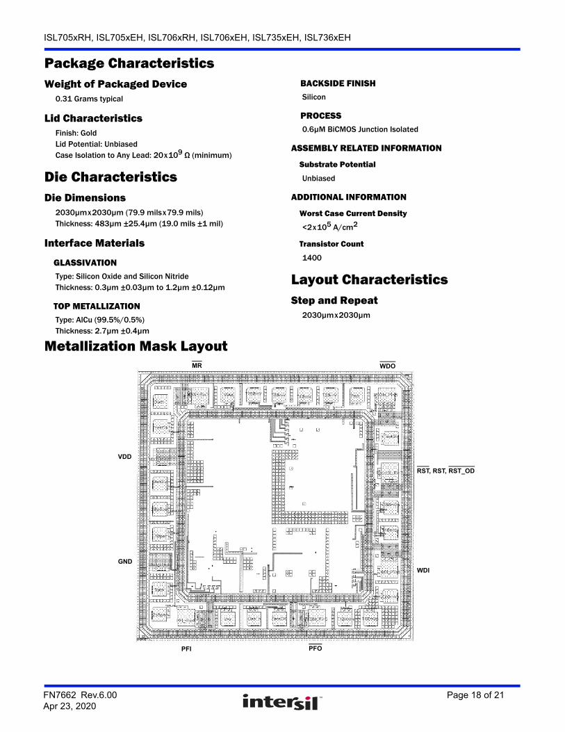
Metallization Mask LayoutWDOMR
VDD
GND
PFI PFO
WDI
RST, RST, RST_OD
FN7662 Rev.6.00 Page 18 of 21Apr 23, 2020
ISL705xRH, ISL705xEH, ISL706xRH, ISL706xEH, ISL735xEH, ISL736xEH
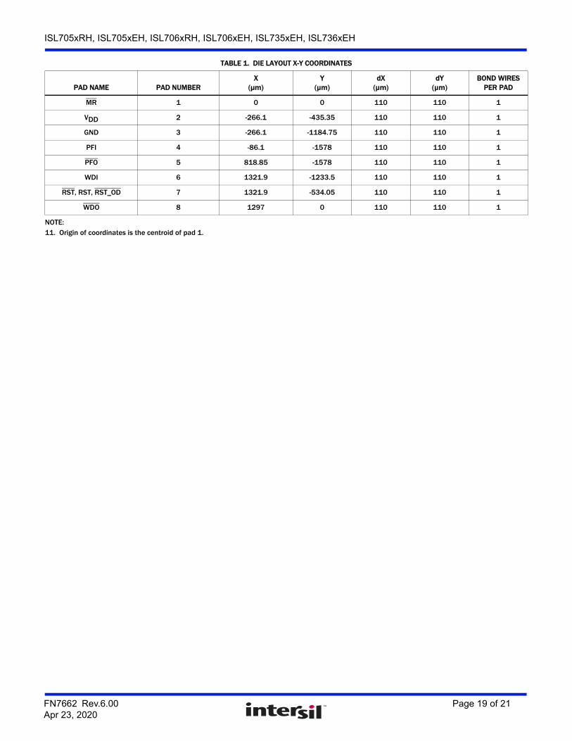
TABLE 1. DIE LAYOUT X-Y COORDINATES
PAD NAME PAD NUMBERX
(µm)Y
(µm)dX
(µm)dY
(µm)BOND WIRES
PER PAD
MR 1 0 0 110 110 1
VDD 2 -266.1 -435.35 110 110 1
GND 3 -266.1 -1184.75 110 110 1
PFI 4 -86.1 -1578 110 110 1
PFO 5 818.85 -1578 110 110 1
WDI 6 1321.9 -1233.5 110 110 1
RST, RST, RST_OD 7 1321.9 -534.05 110 110 1
WDO 8 1297 0 110 110 1
NOTE:11. Origin of coordinates is the centroid of pad 1.
FN7662 Rev.6.00 Page 19 of 21Apr 23, 2020
ISL705xRH, ISL705xEH, ISL706xRH, ISL706xEH, ISL735xEH, ISL736xEH
Revision HistoryThe revision history provided is for informational purposes only and is believed to be accurate, but not warranted. Please visit our website to make sure you have the latest revision.
DATE REVISION CHANGE
Apr 23, 2020 FN7662.6 Added ISL735xEH and ISL736xEH product information throughout datasheet.Updated Rad Hard information on page 1 and ordering information table.Updated Note 4 and added Note 3.Removed About Intersil section.Updated Disclaimer.
February 21, 2017 FN7662.5 Updated Figure 5 on page 6.
July 29, 2016 FN7662.4 Added ISL705EH and ISL706xEH product information throughout datasheet.Updated Figure 4 on page 5.Added Figures 13 and 14.Removed Post Radiation Characteristics table.Updated “Watchdog Timer” on page 15 by removing (1.0s min) reference.Updated “Interface Materials” on page 18 by removing second “Top Metallization” section.
February 10, 2015 FN7662.3 Added part number ISL706CRH to the header of pages 2 through 12, (It had been mistakenly covered up).
December 9, 2014 FN7662.2 Added SEE, ELDRS, and SPICE Model reports to Related Literature on page 1.page 2 added to Ordering Information table:“Specifications for Rad Hard QML devices are controlled by the Defense Logistics Agency Land and Maritime (DLA). The SMD numbers listed in the "Ordering Information" table on page 2 must be used when ordering.”Updated POD on page 21 to most recent revision with following changes:a) Package tkn, ChangedFrom: 0.115/0.070 (2.92/1.18)To: 0.110/0.087 (2.79/2.21)b) Bottom of lead to bottom of package, ChangedFrom: 0.045/0.026” (1.14/0.66)To: 0.036/0.026 (0.92/0.66)c) Lead length, Changed:From: 0.370/0.250 (9.40/6.35)To: 0.370/0.325 (9.40/8.26)d) Lead tkn: On the side view there was a typo on lead tkn, corrected:From: 0.09/0.04 (0.23/0.10)To: 0.009/0.004 (0.23/0.10)Modified Note 2 by adding the words ..."in addition to or instead of”...
November 1, 2011 FN7662.1 Page 13: Updated the transistor count to 1400 from 25000.Pages 7, 9: Removed erroneous overline bars in Figures 8-11.
September 15, 2011 FN7662.0 Initial release
FN7662 Rev.6.00 Page 20 of 21Apr 23, 2020
ISL705xRH, ISL705xEH, ISL706xRH, ISL706xEH, ISL735xEH, ISL736xEH
FN7662 Rev.6.00 Page 21 of 21Apr 23, 2020
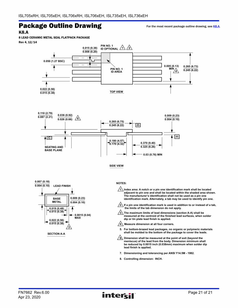
Package Outline DrawingK8.A8 LEAD CERAMIC METAL SEAL FLATPACK PACKAGE
Rev 4, 12/14
LEAD FINISH
SIDE VIEW
TOP VIEW
-D-
-C-
0.265 (6.75)
0.110 (2.79)
0.026 (0.66)
0.265 (6.73)
SEATING AND
0.180 (4.57)
0.03 (0.76) MIN
BASE PLANE
-H-
0.009 (0.23)
0.005 (0.13)PIN NO. 1ID AREA
0.050 (1.27 BSC)
0.022 (0.56)0.015 (0.38)
MIN 0.245 (6.22)
0.087 (2.21)
0.170 (4.32) 0.370 (9.40)
0.325 (8.26)
0.004 (0.10)
0.245 (6.22)
1.adjacent to pin one and shall be located within the shaded area shown. The manufacturer’s identification shall not be used as a pin one identification mark. Alternately, a tab may be used to identify pin one.
2.
3. The maximum limits of lead dimensions (section A-A) shall be measured at the centroid of the finished lead surfaces, when solder dip or tin plate lead finish is applied.
4.
5.shall be molded to the bottom of the package to cover the leads.
6.meniscus) of the lead from the body. Dimension minimum shall be reduced by 0.0015 inch (0.038mm) maximum when solder diplead finish is applied.
7.
8.
NOTES:
0.015 (0.38)0.008 (0.20)
PIN NO. 1ID OPTIONAL 1 2
4
6
3
Dimensioning and tolerancing per ANSI Y14.5M - 1982.
Controlling dimension: INCH.
Index area: A notch or a pin one identification mark shall be located
If a pin one identification mark is used in addition to or instead of a tab,
Measure dimension at all four corners.
For bottom-brazed lead packages, no organic or polymeric materials
Dimension shall be measured at the point of exit (beyond the
SECTION A-A
BASEMETAL
0.007 (0.18)
0.004 (0.10)
0.009 (0.23)
0.004 (0.10)
0.019 (0.48)0.015 (0.38)
0.0015 (0.04)MAX
0.022 (0.56)0.015 (0.38)
0.036 (0.92)
the limits of the tab dimension do not apply.
For the most recent package outline drawing, see K8.A.
Corporate HeadquartersTOYOSU FORESIA, 3-2-24 Toyosu,Koto-ku, Tokyo 135-0061, Japanwww.renesas.com
Contact InformationFor further information on a product, technology, the most up-to-date version of a document, or your nearest sales office, please visit:www.renesas.com/contact/
TrademarksRenesas and the Renesas logo are trademarks of Renesas Electronics Corporation. All trademarks and registered trademarks are the property of their respective owners.
IMPORTANT NOTICE AND DISCLAIMER
RENESAS ELECTRONICS CORPORATION AND ITS SUBSIDIARIES (“RENESAS”) PROVIDES TECHNICAL SPECIFICATIONS AND RELIABILITY DATA (INCLUDING DATASHEETS), DESIGN RESOURCES (INCLUDING REFERENCE DESIGNS), APPLICATION OR OTHER DESIGN ADVICE, WEB TOOLS, SAFETY INFORMATION, AND OTHER RESOURCES “AS IS” AND WITH ALL FAULTS, AND DISCLAIMS ALL WARRANTIES, EXPRESS OR IMPLIED, INCLUDING, WITHOUT LIMITATION, ANY IMPLIED WARRANTIES OF MERCHANTABILITY, FITNESS FOR A PARTICULAR PURPOSE, OR NON-INFRINGEMENT OF THIRD PARTY INTELLECTUAL PROPERTY RIGHTS.
These resources are intended for developers skilled in the art designing with Renesas products. You are solely responsible for (1) selecting the appropriate products for your application, (2) designing, validating, and testing your application, and (3) ensuring your application meets applicable standards, and any other safety, security, or other requirements. These resources are subject to change without notice. Renesas grants you permission to use these resources only for development of an application that uses Renesas products. Other reproduction or use of these resources is strictly prohibited. No license is granted to any other Renesas intellectual property or to any third party intellectual property. Renesas disclaims responsibility for, and you will fully indemnify Renesas and its representatives against, any claims, damages, costs, losses, or liabilities arising out of your use of these resources. Renesas' products are provided only subject to Renesas' Terms and Conditions of Sale or other applicable terms agreed to in writing. No use of any Renesas resources expands or otherwise alters any applicable warranties or warranty disclaimers for these products.
(Rev.1.0 Mar 2020)
© 2020 Renesas Electronics Corporation. All rights reserved.