Embed Size (px)
Citation preview
FN8452Rev 4.00
March 18, 2016
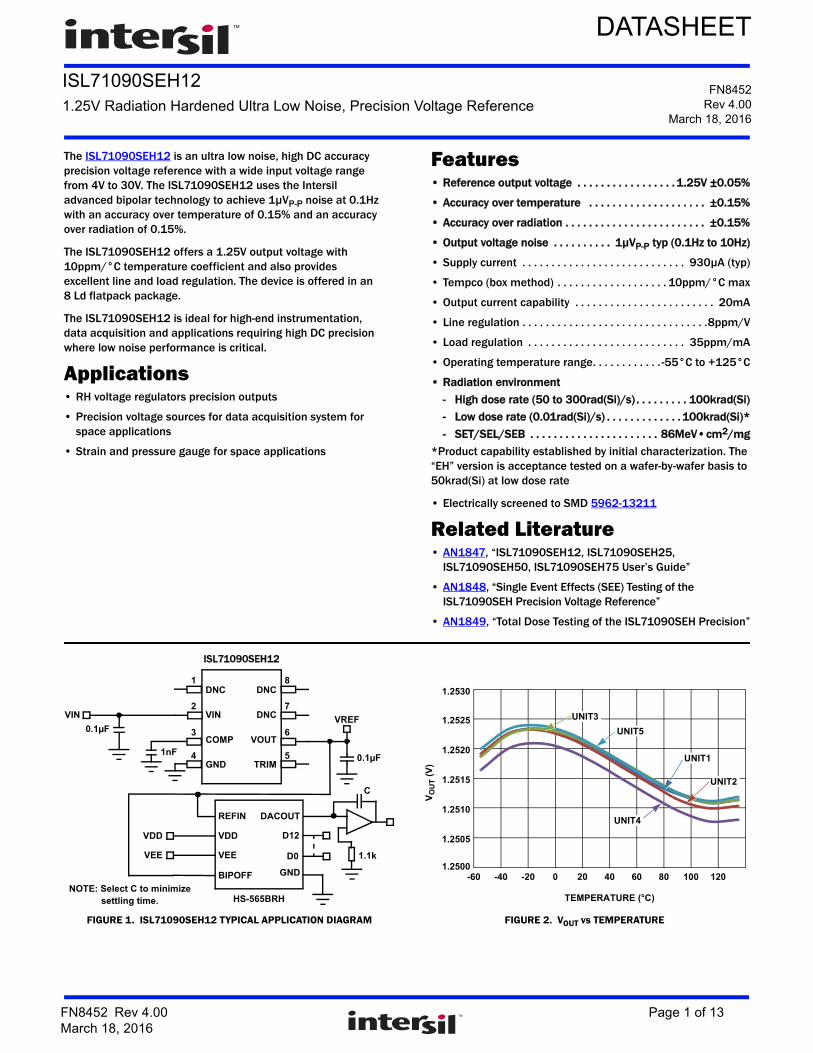
ISL71090SEH121.25V Radiation Hardened Ultra Low Noise, Precision Voltage Reference
DATASHEET
The ISL71090SEH12 is an ultra low noise, high DC accuracy precision voltage reference with a wide input voltage range from 4V to 30V. The ISL71090SEH12 uses the Intersil advanced bipolar technology to achieve 1µVP-P noise at 0.1Hz with an accuracy over temperature of 0.15% and an accuracy over radiation of 0.15%.
The ISL71090SEH12 offers a 1.25V output voltage with 10ppm/°C temperature coefficient and also provides excellent line and load regulation. The device is offered in an 8 Ld flatpack package.
The ISL71090SEH12 is ideal for high-end instrumentation, data acquisition and applications requiring high DC precision where low noise performance is critical.
Applications• RH voltage regulators precision outputs
• Precision voltage sources for data acquisition system for space applications
• Strain and pressure gauge for space applications
Features• Reference output voltage . . . . . . . . . . . . . . . . . 1.25V ±0.05%
• Accuracy over temperature . . . . . . . . . . . . . . . . . . . . ±0.15%
• Accuracy over radiation . . . . . . . . . . . . . . . . . . . . . . . . ±0.15%
• Output voltage noise . . . . . . . . . . 1µVP-P typ (0.1Hz to 10Hz)
• Supply current . . . . . . . . . . . . . . . . . . . . . . . . . . . . 930µA (typ)
• Tempco (box method) . . . . . . . . . . . . . . . . . . . 10ppm/°C max
• Output current capability . . . . . . . . . . . . . . . . . . . . . . . . 20mA
• Line regulation . . . . . . . . . . . . . . . . . . . . . . . . . . . . . . . .8ppm/V
• Load regulation . . . . . . . . . . . . . . . . . . . . . . . . . . . 35ppm/mA
• Operating temperature range. . . . . . . . . . . . -55°C to +125°C
• Radiation environment
- High dose rate (50 to 300rad(Si)/s) . . . . . . . . . 100krad(Si)
- Low dose rate (0.01rad(Si)/s) . . . . . . . . . . . . . 100krad(Si)*
- SET/SEL/SEB . . . . . . . . . . . . . . . . . . . . . . 86MeV•cm2/mg
*Product capability established by initial characterization. The “EH” version is acceptance tested on a wafer-by-wafer basis to 50krad(Si) at low dose rate
• Electrically screened to SMD 5962-13211
Related Literature• AN1847, “ISL71090SEH12, ISL71090SEH25,
ISL71090SEH50, ISL71090SEH75 User’s Guide”
• AN1848, “Single Event Effects (SEE) Testing of the ISL71090SEH Precision Voltage Reference”
• AN1849, “Total Dose Testing of the ISL71090SEH Precision”
FIGURE 1. ISL71090SEH12 TYPICAL APPLICATION DIAGRAM FIGURE 2. VOUT vs TEMPERATURE
0.1µF
VEE
VDD
REFIN
VDD
BIPOFF
VEE
DACOUT
GND
VIN VREF
0.1µF
D0
HS-565BRH
1
2
3
4
6
8
7
5
ISL71090SEH12
D12
1.1k
C
NOTE: Select C to minimizesettling time.
DNC
VIN
COMP
GND
DNC
DNC
VOUT
TRIM1nF
1.2500
1.2505
1.2510
1.2515
1.2520
1.2525
1.2530
-60 -40 -20 0 20 40 60 80 100 120
TEMPERATURE (°C)
UNIT2
UNIT3
UNIT4
UNIT5
VO
UT (
V)
UNIT1
FN8452 Rev 4.00 Page 1 of 13March 18, 2016
ISL71090SEH12
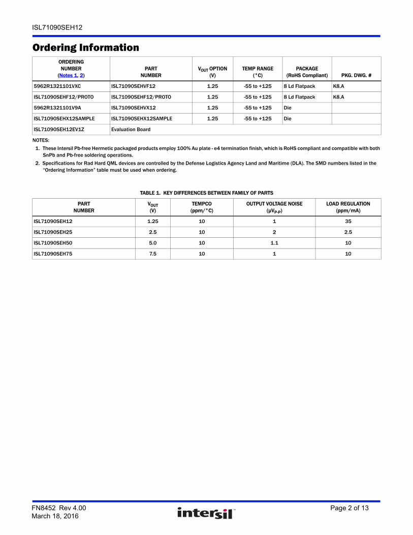
Ordering InformationORDERING NUMBER
(Notes 1, 2)PART
NUMBERVOUT OPTION
(V)TEMP RANGE
(°C)PACKAGE
(RoHS Compliant) PKG. DWG. #
5962R1321101VXC ISL71090SEHVF12 1.25 -55 to +125 8 Ld Flatpack K8.A
ISL71090SEHF12/PROTO ISL71090SEHF12/PROTO 1.25 -55 to +125 8 Ld Flatpack K8.A
5962R1321101V9A ISL71090SEHVX12 1.25 -55 to +125 Die
ISL71090SEHX12SAMPLE ISL71090SEHX12SAMPLE 1.25 -55 to +125 Die
ISL71090SEH12EV1Z Evaluation Board
NOTES:
1. These Intersil Pb-free Hermetic packaged products employ 100% Au plate - e4 termination finish, which is RoHS compliant and compatible with both SnPb and Pb-free soldering operations.
2. Specifications for Rad Hard QML devices are controlled by the Defense Logistics Agency Land and Maritime (DLA). The SMD numbers listed in the “Ordering Information” table must be used when ordering.
TABLE 1. KEY DIFFERENCES BETWEEN FAMILY OF PARTS
PARTNUMBER
VOUT (V)
TEMPCO (ppm/°C)
OUTPUT VOLTAGE NOISE (µVP-P)
LOAD REGULATION (ppm/mA)
ISL71090SEH12 1.25 10 1 35
ISL71090SEH25 2.5 10 2 2.5
ISL71090SEH50 5.0 10 1.1 10
ISL71090SEH75 7.5 10 1 10
FN8452 Rev 4.00 Page 2 of 13March 18, 2016
ISL71090SEH12
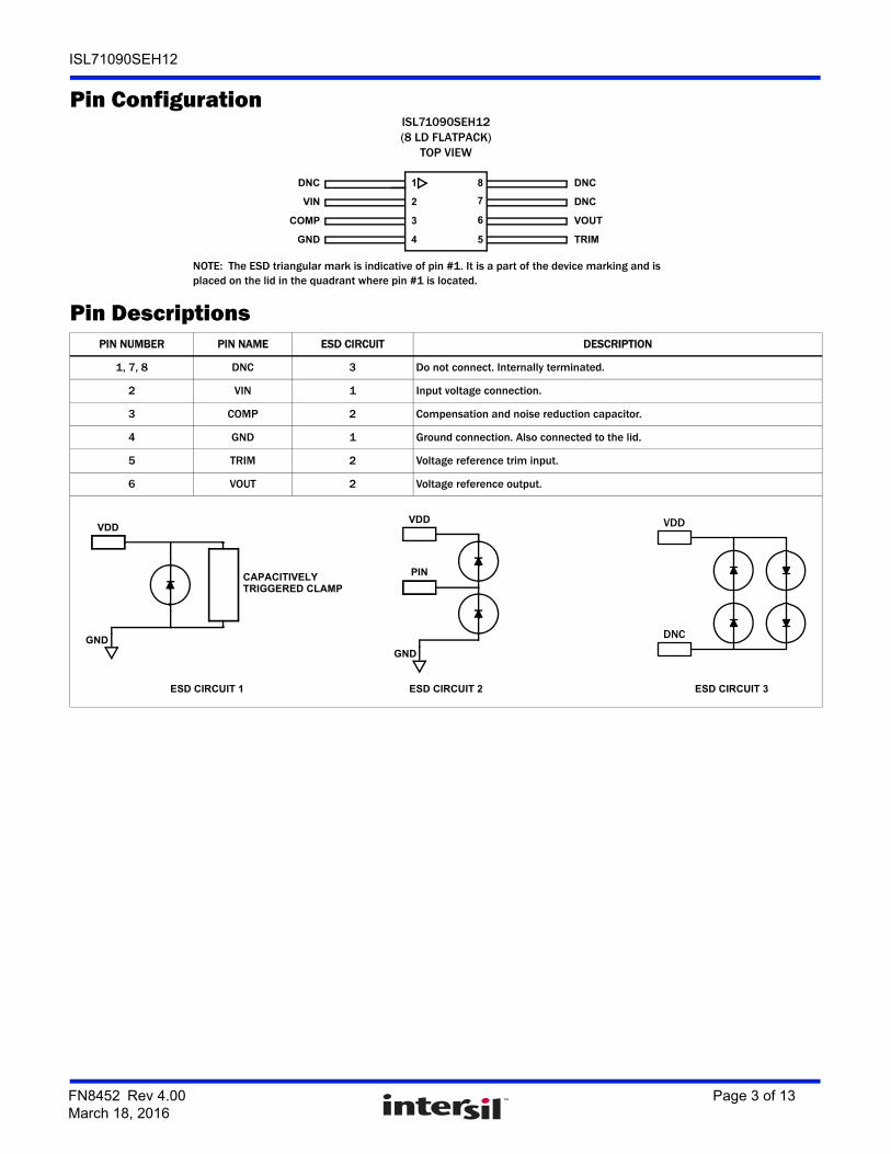
Pin ConfigurationISL71090SEH12(8 LD FLATPACK)
TOP VIEW
8
7
6
5
2
3
4
1DNC
VIN
COMP
GND
DNC
DNC
VOUT
TRIM
NOTE: The ESD triangular mark is indicative of pin #1. It is a part of the device marking and is placed on the lid in the quadrant where pin #1 is located.
Pin DescriptionsPIN NUMBER PIN NAME ESD CIRCUIT DESCRIPTION
1, 7, 8 DNC 3 Do not connect. Internally terminated.
2 VIN 1 Input voltage connection.
3 COMP 2 Compensation and noise reduction capacitor.
4 GND 1 Ground connection. Also connected to the lid.
5 TRIM 2 Voltage reference trim input.
6 VOUT 2 Voltage reference output.
VDD
CAPACITIVELYTRIGGERED CLAMP
GND
VDD
GND
PIN
ESD CIRCUIT 1 ESD CIRCUIT 2 ESD CIRCUIT 3
VDD
DNC
FN8452 Rev 4.00 Page 3 of 13March 18, 2016
ISL71090SEH12
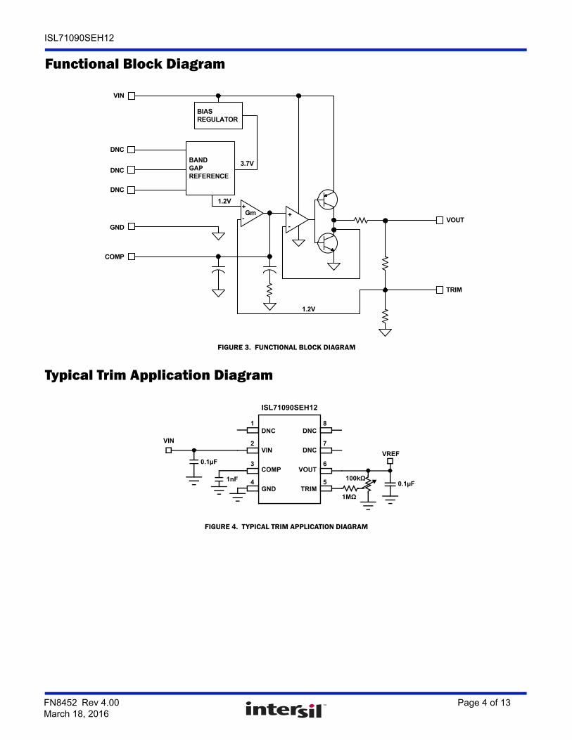
Functional Block Diagram
Typical Trim Application Diagram
COMP
GNDVOUT
TRIM
DNC
DNC
DNC
BIASREGULATOR
VIN
Gm
1.2V
1.2V
3.7V
+
-
+
-
FIGURE 3. FUNCTIONAL BLOCK DIAGRAM
1MΩ
VIN
VREF
0.1µF
1
2
3
4
6
8
7
5
ISL71090SEH12
DNC
VIN
COMP
GND
DNC
DNC
VOUT
TRIM
1nF 100kΩ
0.1µF
FIGURE 4. TYPICAL TRIM APPLICATION DIAGRAM
FN8452 Rev 4.00 Page 4 of 13March 18, 2016
ISL71090SEH12
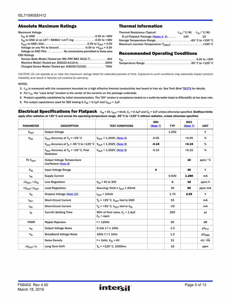
Absolute Maximum Ratings Thermal InformationMaximum Voltage
VIN to GND . . . . . . . . . . . . . . . . . . . . . . . . . . . . . . . . . . . . . . . -0.5V to +40VVIN to GND at an LET = 86MeV•cm2/mg . . . . . . . . . . . . . . -0.5V to +36VVOUT to GND (10s). . . . . . . . . . . . . . . . . . . . . . . . . . . . .-0.5V to VOUT + 0.5VVoltage on any Pin to Ground . . . . . . . . . . . . . . . . . -0.5V to +VOUT + 0.5VVoltage on DNC Pins . . . . . . . . . . . . No connections permitted to these pins
ESD RatingsHuman Body Model (Tested per MIL-PRF-883 3015.7). . . . . . . . . . . 2kVMachine Model (Tested per JESD22-A115-A) . . . . . . . . . . . . . . . . . . 200VCharged Device Model (Tested per JESD22-C101D) . . . . . . . . . . . 750V
Thermal Resistance (Typical) JA (°C/W) JC (°C/W)8 Ld Flatpack Package (Notes 3, 4) . . . . . . 140 15
Storage Temperature Range. . . . . . . . . . . . . . . . . . . . . . . .-65°C to +150°CMaximum Junction Temperature (TJMAX). . . . . . . . . . . . . . . . . . . . . .+150°C
Recommended Operating Conditions VIN . . . . . . . . . . . . . . . . . . . . . . . . . . . . . . . . . . . . . . . . . . . . . . . . 4.0V to +30VTemperature Range . . . . . . . . . . . . . . . . . . . . . . . . . . . . . -55°C to +125°C
CAUTION: Do not operate at or near the maximum ratings listed for extended periods of time. Exposure to such conditions may adversely impact productreliability and result in failures not covered by warranty.
NOTES:
3. JA is measured with the component mounted on a high effective thermal conductivity test board in free air. See Tech Brief TB379 for details.
4. For JC, the "case temp" location is the center of the ceramic on the package underside.
5. Product capability established by initial characterization. The "EH" version is acceptance tested on a wafer-by-wafer basis to 50krad(Si) at low dose rate.
6. The output capacitance used for SEE testing is CIN = 0.1µF and COUT = 1µF.
Electrical Specifications for Flatpack VIN = 5V, IOUT = 0mA, CL = 0.1µF and CC = 1nF unless otherwise specified. Boldface limits apply after radiation at +25°C and across the operating temperature range, -55°C to +125°C without radiation, unless otherwise specified.
PARAMETER DESCRIPTION TEST CONDITIONSMIN
(Note 7) TYPMAX
(Note 7) UNIT
VOUT Output Voltage 1.252 V
VOA VOUT Accuracy at TA = +25°C VOUT = 1.252V, (Note 9) -0.05 +0.05 %
VOUT Accuracy at TA = -55°C to +125°C VOUT = 1.252V, (Note 9) -0.15 +0.15 %
VOUT Accuracy at TA = +25°C, Post Radiation
VOUT = 1.252V, (Note 9) -0.15 +0.15 %
TC VOUT Output Voltage Temperature Coefficient (Note 8)
10 ppm/°C
VIN Input Voltage Range 4 30 V
IIN Supply Current 0.930 1.280 mA
VOUT /VIN Line Regulation VIN = 4V to 30V 8 18 ppm/V
VOUT/IOUT Load Regulation Sourcing: 0mA ≤ IOUT ≤ 20mA 35 55 ppm/mA
VD Dropout Voltage (Note 10) IOUT = 10mA 1.70 2.25 V
ISC+ Short-Circuit Current TA = +25°C, VOUT tied to GND 53 mA
ISC- Short-Circuit Current TA = +25°C, VOUT tied to VIN -23 mA
tR Turn-On Settling Time 90% of final value, CL = 1.0µF, CC = open
250 µs
PSRR Ripple Rejection f = 120Hz 90 dB
eN Output Voltage Noise 0.1Hz ≤ f ≤10Hz 1.0 µVP-P
VN Broadband Voltage Noise 10Hz ≤ f ≤1kHz 1.2 µVRMS
Noise Density f = 1kHz, VIN = 6V 21 nV/Hz
VOUT/t Long Term Drift TA = +125°C, 1000hrs 15 ppm
FN8452 Rev 4.00 Page 5 of 13March 18, 2016
ISL71090SEH12
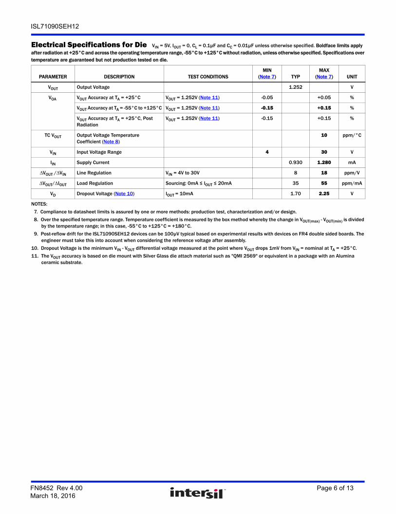
Electrical Specifications for Die VIN = 5V, IOUT = 0, CL = 0.1µF and CC = 0.01µF unless otherwise specified. Boldface limits apply after radiation at +25°C and across the operating temperature range, -55°C to +125°C without radiation, unless otherwise specified. Specifications over temperature are guaranteed but not production tested on die.
PARAMETER DESCRIPTION TEST CONDITIONSMIN
(Note 7) TYPMAX
(Note 7) UNIT
VOUT Output Voltage 1.252 V
VOA VOUT Accuracy at TA = +25°C VOUT = 1.252V (Note 11) -0.05 +0.05 %
VOUT Accuracy at TA = -55°C to +125°C VOUT = 1.252V (Note 11) -0.15 +0.15 %
VOUT Accuracy at TA = +25°C, Post Radiation
VOUT = 1.252V (Note 11) -0.15 +0.15 %
TC VOUT Output Voltage Temperature Coefficient (Note 8)
10 ppm/°C
VIN Input Voltage Range 4 30 V
IIN Supply Current 0.930 1.280 mA
VOUT /VIN Line Regulation VIN = 4V to 30V 8 18 ppm/V
VOUT/IOUT Load Regulation Sourcing: 0mA ≤ IOUT ≤ 20mA 35 55 ppm/mA
VD Dropout Voltage (Note 10) IOUT = 10mA 1.70 2.25 V
NOTES:
7. Compliance to datasheet limits is assured by one or more methods: production test, characterization and/or design.
8. Over the specified temperature range. Temperature coefficient is measured by the box method whereby the change in VOUT(max) - VOUT(min) is divided by the temperature range; in this case, -55°C to +125°C = +180°C.
9. Post-reflow drift for the ISL71090SEH12 devices can be 100µV typical based on experimental results with devices on FR4 double sided boards. The engineer must take this into account when considering the reference voltage after assembly.
10. Dropout Voltage is the minimum VIN - VOUT differential voltage measured at the point where VOUT drops 1mV from VIN = nominal at TA = +25°C.
11. The VOUT accuracy is based on die mount with Silver Glass die attach material such as "QMI 2569" or equivalent in a package with an Alumina ceramic substrate.
FN8452 Rev 4.00 Page 6 of 13March 18, 2016
ISL71090SEH12
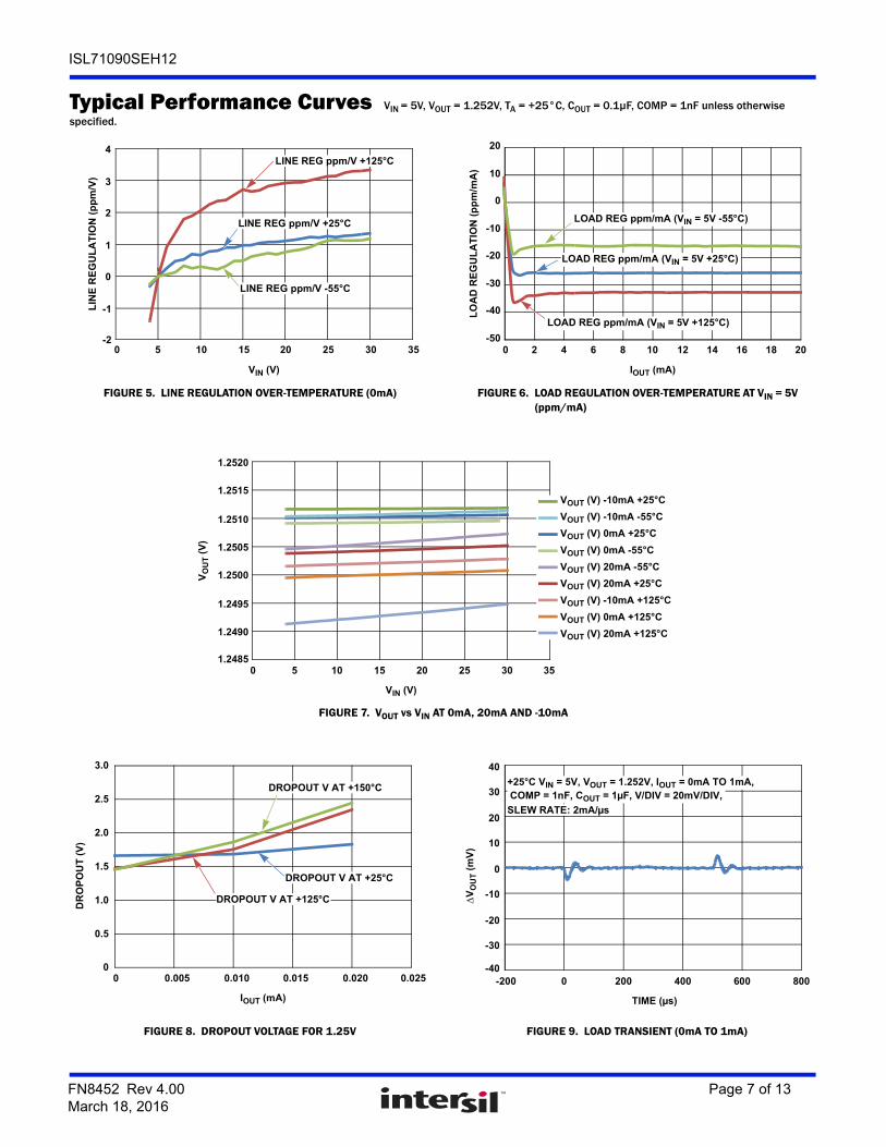
Typical Performance Curves VIN = 5V, VOUT = 1.252V, TA = +25°C, COUT = 0.1µF, COMP = 1nF unless otherwise specified.
FIGURE 5. LINE REGULATION OVER-TEMPERATURE (0mA) FIGURE 6. LOAD REGULATION OVER-TEMPERATURE AT VIN = 5V (ppm/mA)
FIGURE 7. VOUT vs VIN AT 0mA, 20mA AND -10mA
FIGURE 8. DROPOUT VOLTAGE FOR 1.25V FIGURE 9. LOAD TRANSIENT (0mA TO 1mA)
-2
-1
0
1
2
3
4
LIN
E R
EG
UL
AT
ION
(p
pm
/V)
LINE REG ppm/V +25°C
LINE REG ppm/V +125°C
LINE REG ppm/V -55°C
VIN (V)
0 5 10 15 20 25 30 35
LO
AD
RE
GU
LA
TIO
N (
pp
m/m
A)
IOUT (mA)
-50
-40
-30
-20
-10
0
10
20
0 2 4 6 8 10 12 14 16 18 20
LOAD REG ppm/mA (VIN = 5V +125°C)
LOAD REG ppm/mA (VIN = 5V +25°C)
LOAD REG ppm/mA (VIN = 5V -55°C)
0 5 10 15 20 25 30 35
VIN (V)
VO
UT (
V)
1.2485
1.2490
1.2495
1.2500
1.2505
1.2510
1.2515
1.2520
VOUT (V) 0mA +25°C
VOUT (V) 20mA +25°C
VOUT (V) -10mA +25°C
VOUT (V) 0mA +125°C
VOUT (V) 20mA +125°C
VOUT (V) -10mA +125°C
VOUT (V) 0mA -55°C
VOUT (V) 20mA -55°C
VOUT (V) -10mA -55°C
0.5
1.0
1.5
2.0
2.5
3.0
0.005 0.010 0.015 0.020 0.0250
0
DROPOUT V AT +25°C
DROPOUT V AT +125°C
DROPOUT V AT +150°C
IOUT (mA)
DR
OP
OU
T (
V)
TIME (µs)
-200-40
-30
-20
-10
0
10
20
30
40
0 200 400 600 800
V
OU
T (
mV
)
+25°C VIN = 5V, VOUT = 1.252V, IOUT = 0mA TO 1mA, COMP = 1nF, COUT = 1µF, V/DIV = 20mV/DIV,
SLEW RATE: 2mA/µs
FN8452 Rev 4.00 Page 7 of 13March 18, 2016
ISL71090SEH12
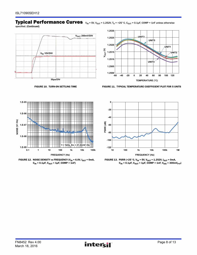
FIGURE 10. TURN-ON SETTLING TIME FIGURE 11. TYPICAL TEMPERATURE COEFFICIENT PLOT FOR 5 UNITS
FIGURE 12. NOISE DENSITY vs FREQUENCY (VIN = 6.0V, IOUT = 0mA, CIN = 0.1µF, COUT = 1µF, COMP = 1nF)
FIGURE 13. PSRR (+25°C, VIN = 5V, VOUT = 1.252V, IOUT = 0mA, CIN = 0.1µF, COUT = 1µF, COMP = 1nF, VSIG = 300mVP-P)
Typical Performance Curves VIN = 5V, VOUT = 1.252V, TA = +25°C, COUT = 0.1µF, COMP = 1nF unless otherwise specified. (Continued)
VOUT 200mV/DIV
50µs/DIV
VIN 10V/DIV
1.2500
1.2505
1.2510
1.2515
1.2520
1.2525
1.2530
-60 -40 -20 0 20 40 60 80 100 120
TEMPERATURE (°C)
UNIT2
UNIT3
UNIT4
UNIT5
VO
UT (
V)
UNIT1
1.E-09
1.E-08
1.E-07
1.E-06
1.E-05
0.1 1 10 100 1k 10k 100k
NO
ISE
(V
/√H
z)
FREQUENCY (Hz)
f = 1kHz, En = 21.02nV/√Hz-120
-100
-80
-60
-40
-20
0
10 100 1k 10k 100k 1M
PS
RR
(d
B)
FREQUENCY (Hz)
FN8452 Rev 4.00 Page 8 of 13March 18, 2016
ISL71090SEH12
Device OperationBandgap Precision ReferenceThe ISL71090SEH12 uses a bandgap architecture and special trimming circuitry to produce a temperature compensated, precision voltage reference with high input voltage capability and moderate output current drive.
Applications InformationBoard Mounting ConsiderationsFor applications requiring the highest accuracy, board mounting location should be reviewed. The device uses a ceramic flatpack package. Generally, mild stresses to the die when the Printed Circuit (PC) board is heated and cooled, can slightly change the shape. Because of these die stresses, placing the device in areas subject to slight twisting can cause degradation of reference voltage accuracy. It is normally best to place the device near the edge of a board, or on the shortest side, because the axis of bending is most limited in that location. Mounting the device in a cutout also minimizes flex. Obviously, mounting the device on flexprint or extremely thin PC material will likewise cause loss of reference accuracy.
Board Assembly ConsiderationsSome PC board assembly precautions are necessary. Normal output voltage shifts of typically 100µV can be expected with Pb-free reflow profiles or wave solder on multilayer FR4 PC boards. Precautions should be taken to avoid excessive heat or extended exposure to high reflow or wave solder temperatures.
Noise Performance and ReductionThe output noise voltage over the 0.1Hz to 10Hz bandwidth is typically 1µVP-P. The noise measurement is made with a 9.9Hz bandpass filter. Noise in the 10Hz to 1kHz bandwidth is approximately 1.6µVRMS, with 0.1µF capacitance on the output. This noise measurement is made with a bandpass filter of 990Hz. Load capacitance up to 10µF (with COMP capacitor from Table 2) can be added but will result in only marginal improvements in output noise and transient response.
Turn-On TimeNormal turn-on time is typically 250µs, the circuit designer must take this into account when looking at power-up delays or sequencing.
Temperature CoefficientThe limits stated for Temperature Coefficient (Tempco) are governed by the method of measurement. The overwhelming standard for specifying the temperature drift of a reference is to measure the reference voltage at two temperatures, which provide for the maximum voltage deviation and take the total variation, (VHIGH - VLOW), this is then divided by the temperature extremes of measurement (THIGH – TLOW). The result is divided by the nominal reference voltage (at T = +25°C) and multiplied by 106 to yield ppm/°C. This is the “Box” method for specifying temperature coefficient.
Output Voltage AdjustmentThe output voltage can be adjusted above and below the factory-calibrated value via the trim terminal. The trim terminal is the negative feedback divider point of the output op amp. The voltage at the trim pin is set at approximately 1.216V by the internal bandgap and amplifier circuitry of the voltage reference. The suggested method to adjust the output is to connect a 1MΩ external resistor directly to the trim terminal and connect the other end to the wiper of a potentiometer that has a 100kΩ resistance and whose outer terminals connect to VOUT and ground. If a 1MΩ resistor is connected to trim, the output adjust range will be ±6.3mV. The TRIM pin should not have any capacitor tied to its output, also it is important to minimize the capacitance on the trim terminal during layout to preserve output amplifier stability. It is also best to connect the series resistor directly to the trim terminal, to minimize that capacitance and also to minimize noise injection. Small trim adjustments will not disturb the factory-set temperature coefficient of the reference, but trimming near the extreme values can.
Output StageThe output stage of the device has a push-pull configuration with a high-side PNP and a low-side NPN. This helps the device to act as a source and sink. The device can source 20mA.
Use of COMP CapacitorThe reference can be compensated for the COUT capacitors used by adding a capacitor from COMP pin to GND. See Table 2 for recommended values of the COMP capacitor.
SEE TestingThe device was tested under ion beam at an LET of 86MeV•cm2/mg. The device did not latch up or burn out to a VDD of 36V and at +125°C. Single Event transients were observed and are summarized in Table 3:
DNC PinsThese pins are for trimming purpose and for factory use only. Do not connect these to the circuit in any way. It will adversely effect the performance of the reference.
TABLE 2. RECOMMENDED VALUES OF COMP CAPACITOR
COUT(µF)
CCOMP(nF)
0.1 1
1 10
10 30
TABLE 3. OBSERVATION OF SINGLE EVENT TRANSIENTS
VIN(V)
IOUT(mA)
COUT(µF)
SET(% VOUT)
4 5 1 -4.6
30 5 1 -4.4
30 5 10 -1.0
FN8452 Rev 4.00 Page 9 of 13March 18, 2016
ISL71090SEH12
Package CharacteristicsWeight of Packaged Device
0. 31 Grams (Typical)
Lid CharacteristicsFinish: GoldPotential: Connected to lead #4 (GND)Case Isolation to Any Lead: 20 x 109 Ω (min)
Die CharacteristicsDie Dimensions
1464µm x 1744µm (58 mils x 69 mils)Thickness: 483µm ± 25µm (19 mils ± 1 mil)
Interface Materials
GLASSIVATIONType: NitroxThickness: 15kÅ
Top Metallization
Type: AlCu (99.5%/0.5%)Thickness: 30kÅ
BACKSIDE FINISH Silicon
ASSEMBLY RELATED INFORMATION
SUBSTRATE POTENTIALFloating
ADDITIONAL INFORMATION
WORST CASE CURRENT DENSITY<2 x 10⁵ A/cm2
PROCESSDielectrically Isolated Advanced Bipolar Technology- PR40 SOI
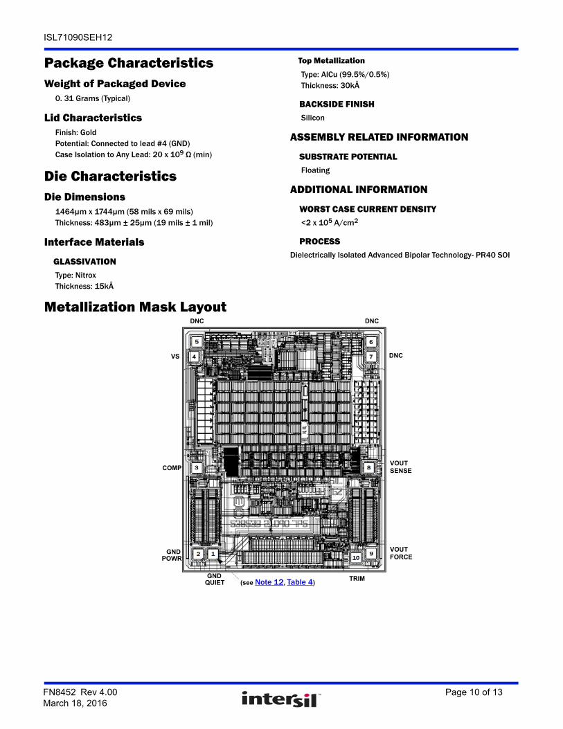
Metallization Mask Layout
GND
GNDPOWR
QUIET
COMP
VS
DNC DNC
DNC
VOUTSENSE
VOUTFORCE
TRIM(see Note 12, Table 4)
FN8452 Rev 4.00 Page 10 of 13March 18, 2016
ISL71090SEH12
TABLE 4. DIE LAYOUT X-Y COORDINATES
PAD NAME PAD NUMBERX
(µm)Y
(µm) BOND WIRES PER PAD
GND PWR 2 -104 0 1
GND QUIET 1 0 0 1
COMP 3 -108 589 1
VS 4 -125 1350 1
DNC 5 -108 1452 1
DNC 6 1089 1452 1
DNC 7 1089 1350 1
VOUT SENSE 8 1072 598 1
VOUT FORCE 9 1088 1 1
TRIM 10 985 -25 1
NOTES:
12. Origin of coordinates is the centroid of GND QUIET.
13. Bond wire size is 1.0 mil.
Revision HistoryThe revision history provided is for informational purposes only and is believed to be accurate, but not warranted. Please go to the web to make sure that you have the latest revision.
DATE REVISION CHANGE
March 18, 2016 FN8452.4 -Changed title from “Radiation Hardened Ultra Low Noise, Precision Voltage Reference” to “1.25V Radiation Hardened Ultra Low Noise, Precision Voltage Reference”-Updated Related Literature document titles to match titles on the actual documents.-Added Table 1 on page 2.On page 5:
-Changed Electrical Specification for Flatpack note from: "Boldface limits apply over the operating temperature range, -55°C to +125°C and radiation." To: "Boldface limits apply after radiation at +25°C or across the operating temperature range, -55°C to +125°C without radiation, unless otherwise specified.-For parameter VOA (row 4) in Electrical Specifications for Flatpack table changed description from: "VOUT Accuracy, Post Rad", to: "VOUT Accuracy at TA = +25°C, Post Rad" and for parameters VOA (rows 2, 3, 4) added "Note 9" to Conditions column.
On page 6:-Changed Electrical Specification for Die note from: "Boldface limits apply over the operating temperature range, -55°C to +125°C and radiation." To: "Boldface limits apply after radiation at +25°C or across the operating temperature range, -55°C to +125°C without radiation, unless otherwise specified.- Added "VOA Post Rad" parameter, and for VOA (rows 2, 3, and 4) parameters added "Note 11" to Conditions column.
August 14, 2015 FN8452.3 Updated second sentence on page 1From: The ISL71090SEH12 uses the Intersil Advanced Bipolar technology to achieve sub 1µVP-P noise at 0.1Hz with an accuracy over temperature and radiation of 0.15%.To: The ISL71090SEH12 uses the Intersil Advanced Bipolar technology to achieve sub 1µVP-P noise at 0.1Hz with an accuracy over temperature of 0.15% and an accuracy over radiation of 0.15%.Updated Features to have accuracy over-temperature and radiation on separate linesUpdated output capacitor in Figure 1 from 1µF to 0.1µF.Added “Typical Trim Application Diagram” on page 4Added in Electrical Spec Table “VOUT Accuracy at TA = +25°C, Post Radiation” on page 5Updated Table 2 on page 9 second and last rows from 1, 1, 10, 10 to 1, 10, 10, 30 and added titles to both Tables 2 and 3.Updated POD K8.A to most recent revision. Change is as follows: Modified Note 2 by adding the words ...”in addition to or instead of”...
FN8452 Rev 4.00 Page 11 of 13March 18, 2016
ISL71090SEH12
Intersil products are manufactured, assembled and tested utilizing ISO9001 quality systems as notedin the quality certifications found at www.intersil.com/en/support/qualandreliability.html
Intersil products are sold by description only. Intersil may modify the circuit design and/or specifications of products at any time without notice, provided that such modification does not, in Intersil's sole judgment, affect the form, fit or function of the product. Accordingly, the reader is cautioned to verify that datasheets are current before placing orders. Information furnished by Intersil is believed to be accurate and reliable. However, no responsibility is assumed by Intersil or its subsidiaries for its use; nor for any infringements of patents or other rights of third parties which may result from its use. No license is granted by implication or otherwise under any patent or patent rights of Intersil or its subsidiaries.
For information regarding Intersil Corporation and its products, see www.intersil.com
For additional products, see www.intersil.com/en/products.html
© Copyright Intersil Americas LLC 2013-2016. All Rights Reserved.All trademarks and registered trademarks are the property of their respective owners.
About IntersilIntersil Corporation is a leading provider of innovative power management and precision analog solutions. The company's products address some of the largest markets within the industrial and infrastructure, mobile computing and high-end consumer markets.
For the most updated datasheet, application notes, related documentation and related parts, please see the respective product information page found at www.intersil.com.
You may report errors or suggestions for improving this datasheet by visiting www.intersil.com/ask.
Reliability reports are also available from our website at www.intersil.com/support
September 13, 2013 FN8452.2 Changed the output voltage noise value from 2µVP-P to 1µVP-P throughout the datasheet.Figures 7, 11 changed VOUT value from VOUT = 1.25 to VOUT = 1.252Removed (VOUT = 1.25V) from “Noise Performance and Reduction” section.Updated Related Literature on page 1, as follow: Changed the link from AN1863 to AN1848 and AN1864 to AN1849. Changed SEH12 to SEHXX.Electrical specifications table for output voltage (VOUT) on page 5 and page 6 : Removed VIN = 5V from conditions cell.Electrical specifications table for dropout voltage on page 5 and page 6: Changed VOUT = 1.25V @ 10mA to IOUT @ 10mA. Electrical specifications table for V0A on page 5 and page 6: Updated conditions cell from VOUT = 1.25V TO VOUT=1.252V.Electrical specifications table for Flatpack on page 5 as follow: Removed VOUT = 1.25V from Input Voltage Range, Line Regulation, Dropout Voltage, Output Voltage Noise, Broadband Voltage Noise, Noise Density.Electrical specifications table for Die on page 6 as follow: Removed VOUT = 1.25V from Input Voltage Range, Line Regulation, Dropout Voltage.Figure7 on page 6: Added slew rate: 2 mA/us.Typical Performance Curves on page 7 added to header: “COUT = 0.1µF, COMP = 1nF”.Added die sale part number to Electrical spec table on page 6.Electrical Spec on page 5: Changed CC = 0.02µF to CC = 1nF and changed IOUT = 0 to IOUT = 0mA.Added the part numbers ISL71090SEHVX12 and ISL71090SEHX12SAMPLE to ordering information table on page 2. Figure 1 on page 1: Added 1nF cap on comp pin. Added a note to Pin Configuration on page 3.Removed a note from Electrical spec table on page 6.
August 8, 2013 FN8452.1 Update app note link in Related literature from AN1862 to AN1847.
June 26, 2013 FN8452.0 Initial Release.
Revision HistoryThe revision history provided is for informational purposes only and is believed to be accurate, but not warranted. Please go to the web to make sure that you have the latest revision. (Continued)
DATE REVISION CHANGE
FN8452 Rev 4.00 Page 12 of 13March 18, 2016
ISL71090SEH12
FN8452 Rev 4.00 Page 13 of 13March 18, 2016
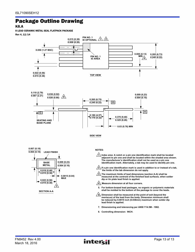
Package Outline DrawingK8.A8 LEAD CERAMIC METAL SEAL FLATPACK PACKAGE
Rev 4, 12/14
LEAD FINISH
SIDE VIEW
TOP VIEW
-D-
-C-
0.265 (6.75)
0.110 (2.79)
0.026 (0.66)
0.265 (6.73)
SEATING AND
0.180 (4.57)
0.03 (0.76) MIN
BASE PLANE
-H-
0.009 (0.23)
0.005 (0.13)PIN NO. 1ID AREA
0.050 (1.27 BSC)
0.022 (0.56)0.015 (0.38)
MIN 0.245 (6.22)
0.087 (2.21)
0.170 (4.32) 0.370 (9.40)
0.325 (8.26)
0.004 (0.10)
0.245 (6.22)
1.adjacent to pin one and shall be located within the shaded area shown. The manufacturer’s identification shall not be used as a pin one identification mark. Alternately, a tab may be used to identify pin one.
2.
3. The maximum limits of lead dimensions (section A-A) shall be measured at the centroid of the finished lead surfaces, when solder dip or tin plate lead finish is applied.
4.
5.shall be molded to the bottom of the package to cover the leads.
6.meniscus) of the lead from the body. Dimension minimum shall be reduced by 0.0015 inch (0.038mm) maximum when solder diplead finish is applied.
7.
8.
NOTES:
0.015 (0.38)0.008 (0.20)
PIN NO. 1ID OPTIONAL 1 2
4
6
3
Dimensioning and tolerancing per ANSI Y14.5M - 1982.
Controlling dimension: INCH.
Index area: A notch or a pin one identification mark shall be located
If a pin one identification mark is used in addition to or instead of a tab,
Measure dimension at all four corners.
For bottom-brazed lead packages, no organic or polymeric materials
Dimension shall be measured at the point of exit (beyond the
SECTION A-A
BASEMETAL
0.007 (0.18)
0.004 (0.10)
0.009 (0.23)
0.004 (0.10)
0.019 (0.48)0.015 (0.38)
0.0015 (0.04)MAX
0.022 (0.56)0.015 (0.38)
0.036 (0.92)
the limits of the tab dimension do not apply.