Embed Size (px)
Citation preview
FN8418Rev 5.00
Jan 28, 2022
ISL91127High Efficiency Buck-Boost Regulator with 4.5A Switches
DATASHEET
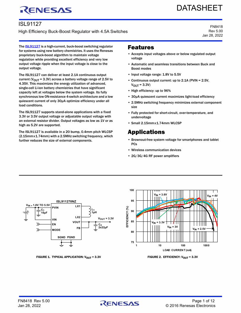
The ISL91127 is a high-current, buck-boost switching regulator for systems using new battery chemistries. It uses the Renesas proprietary buck-boost algorithm to maintain voltage regulation while providing excellent efficiency and very low output voltage ripple when the input voltage is close to the output voltage.
The ISL91127 can deliver at least 2.1A continuous output current (VOUT = 3.3V) across a battery voltage range of 2.5V to 4.35V. This maximizes the energy utilization of advanced, single-cell Li-ion battery chemistries that have significant capacity left at voltages below the system voltage. Its fully synchronous low ON-resistance 4-switch architecture and a low quiescent current of only 30µA optimize efficiency under all load conditions.
The ISL91127 supports stand-alone applications with a fixed 3.3V or 3.5V output voltage or adjustable output voltage with an external resistor divider. Output voltages as low as 1V or as high as 5.2V are supported.
The ISL91127 is available in a 20 bump, 0.4mm pitch WLCSP (2.15mmx1.74mm) with a 2.5MHz switching frequency, which further reduces the size of external components.
Features• Accepts input voltages above or below regulated output
voltage
• Automatic and seamless transitions between Buck and Boost modes
• Input voltage range: 1.8V to 5.5V
• Continuous output current: up to 2.1A (PVIN = 2.5V, VOUT = 3.3V)
• High efficiency: up to 96%
• 30µA quiescent current maximizes light-load efficiency
• 2.5MHz switching frequency minimizes external component size
• Fully protected for short-circuit, over-temperature, and undervoltage
• Small 2.15mmx1.74mm WLCSP
Applications• Brownout-free system voltage for smartphones and tablet
PCs
• Wireless communication devices
• 2G/3G/4G RF power amplifiers
FIGURE 1. TYPICAL APPLICATION: VOUT = 3.3V FIGURE 2. EFFICIENCY: VOUT = 3.3V
PVINVIN = 1.8V TO 5.5V
VOUT = 3.3V
ISL91127IINZ
VINEN
LX1
LX2
VOUT
FB
SGND PGND
C110µF
L11µH
C22x22µF
MODE
75
80
85
90
95
100
1 10 100 1000LOAD CURREN T (mA)
VIN = 3VVIN = 3.3V
VIN = 4VVIN = 3.6V
VIN = 2.5V
EFFI
CIE
NC
Y (%
)
FN8418 Rev 5.00 Page 1 of 12Jan 28, 2022 © 2016 Renesas Electronics

ISL91127
Pin ConfigurationISL91127
(20 BALL WLCSP, 0.4mm PITCH)TOP VIEW, BUMPS DOWN
Block Diagram
FIGURE 3. BLOCK DIAGRAM
OSC
ERROR AMP
PVIN
PWM CONTROL
PVIN MONITOR
LX1
VREF
REF
REV
ERSE
C
URR
ENT
VOUTA2
B2 D2LX2
GATE DRIVERS
AND ANTI-SHOOT THRU
A4VIN
THERMALSHUTDOWN
CURRENTDETECT
E2
VOUTMONITOR
B4EN
E4 FB
C2 PGND
D4SGND EN
EN
EN
EN
EN
VOUTCLAMP
C3
VOLTAGEPROG.
EN
SOFTDISCHARGE
A1B3 D3
E1B1
A3 E3
D1
C1
MODE
C4
PVIN PVIN
LX1 LX1
SGND
FB
MODE
EN
VIN
PGND PGND
LX2 LX2
VOUT VOUT
LX2
VOUT
LX1
PVIN
SGND
1
A
2 3 4
B
C
D
E
Pin DescriptionsPIN # PIN NAMES DESCRIPTION
A1, A2, A3 PVIN Power input. Range: 1.8V to 5.5V. Connect 2x10μF capacitors to PGND.
B1, B2, B3 LX1 Inductor connection, input side
C1, C2 PGND Power ground for high switching current
D1, D2, D3 LX2 Inductor connection, output side
E1, E2,E3
VOUT Buck-boost regulator output. Connect 2x22μF capacitors to PGND.
C3 MODE Logic input, HIGH for auto PFM mode. LOWfor forced PWM operation.
A4 VIN Supply input. Range: 1.8V to 5.5V.
B4 EN Logic input, drive HIGH to enable device.
C4, D4 SGND Analog ground pin
E4 FB Voltage feedback pin
FN8418 Rev 5.00 Page 2 of 12Jan 28, 2022
ISL91127
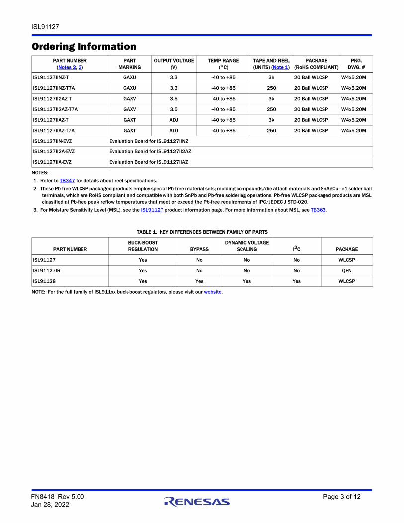
Ordering InformationPART NUMBER
(Notes 2, 3)PART
MARKINGOUTPUT VOLTAGE
(V)TEMP RANGE
(°C)TAPE AND REEL(UNITS) (Note 1)
PACKAGE(RoHS COMPLIANT)
PKG. DWG. #
ISL91127IINZ-T GAXU 3.3 -40 to +85 3k 20 Ball WLCSP W4x5.20M
ISL91127IINZ-T7A GAXU 3.3 -40 to +85 250 20 Ball WLCSP W4x5.20M
ISL91127II2AZ-T GAXV 3.5 -40 to +85 3k 20 Ball WLCSP W4x5.20M
ISL91127II2AZ-T7A GAXV 3.5 -40 to +85 250 20 Ball WLCSP W4x5.20M
ISL91127IIAZ-T GAXT ADJ -40 to +85 3k 20 Ball WLCSP W4x5.20M
ISL91127IIAZ-T7A GAXT ADJ -40 to +85 250 20 Ball WLCSP W4x5.20M
ISL91127IIN-EVZ Evaluation Board for ISL91127IINZ
ISL91127II2A-EVZ Evaluation Board for ISL91127II2AZ
ISL91127IIA-EVZ Evaluation Board for ISL91127IIAZ
NOTES:1. Refer to TB347 for details about reel specifications.2. These Pb-free WLCSP packaged products employ special Pb-free material sets; molding compounds/die attach materials and SnAgCu - e1 solder ball
terminals, which are RoHS compliant and compatible with both SnPb and Pb-free soldering operations. Pb-free WLCSP packaged products are MSL classified at Pb-free peak reflow temperatures that meet or exceed the Pb-free requirements of IPC/JEDEC J STD-020.
3. For Moisture Sensitivity Level (MSL), see the ISL91127 product information page. For more information about MSL, see TB363.
TABLE 1. KEY DIFFERENCES BETWEEN FAMILY OF PARTS
PART NUMBERBUCK-BOOSTREGULATION BYPASS
DYNAMIC VOLTAGE SCALING I2C PACKAGE
ISL91127 Yes No No No WLCSP
ISL91127IR Yes No No No QFN
ISL91128 Yes Yes Yes Yes WLCSP
NOTE: For the full family of ISL911xx buck-boost regulators, please visit our website.
FN8418 Rev 5.00 Page 3 of 12Jan 28, 2022
ISL91127
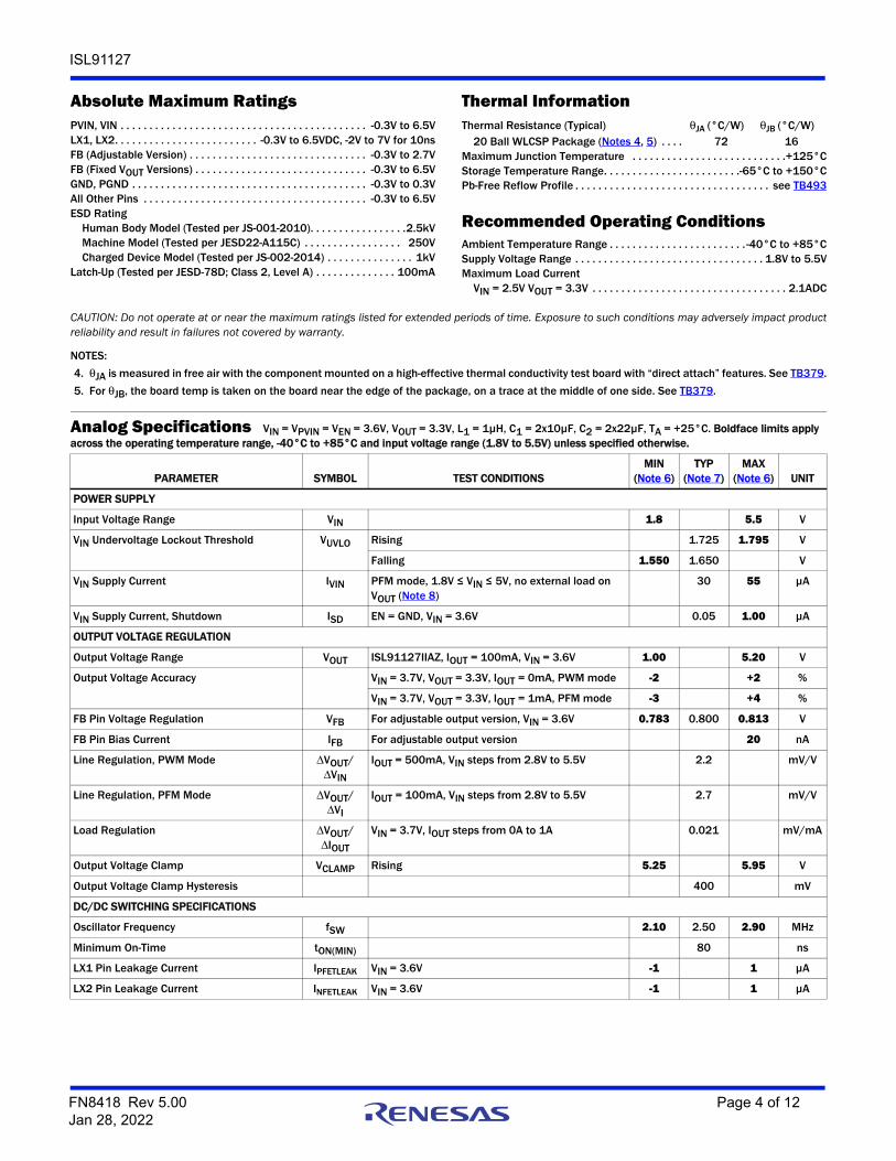
Absolute Maximum Ratings Thermal InformationPVIN, VIN . . . . . . . . . . . . . . . . . . . . . . . . . . . . . . . . . . . . . . . . . . . -0.3V to 6.5VLX1, LX2. . . . . . . . . . . . . . . . . . . . . . . . . -0.3V to 6.5VDC, -2V to 7V for 10nsFB (Adjustable Version) . . . . . . . . . . . . . . . . . . . . . . . . . . . . . . . -0.3V to 2.7VFB (Fixed VOUT Versions) . . . . . . . . . . . . . . . . . . . . . . . . . . . . . . -0.3V to 6.5VGND, PGND . . . . . . . . . . . . . . . . . . . . . . . . . . . . . . . . . . . . . . . . . -0.3V to 0.3VAll Other Pins . . . . . . . . . . . . . . . . . . . . . . . . . . . . . . . . . . . . . . . -0.3V to 6.5VESD Rating
Human Body Model (Tested per JS-001-2010). . . . . . . . . . . . . . . . .2.5kVMachine Model (Tested per JESD22-A115C) . . . . . . . . . . . . . . . . . 250VCharged Device Model (Tested per JS-002-2014) . . . . . . . . . . . . . . . 1kV
Latch-Up (Tested per JESD-78D; Class 2, Level A) . . . . . . . . . . . . . . 100mA
Thermal Resistance (Typical) θJA (°C/W) θJB (°C/W)20 Ball WLCSP Package (Notes 4, 5) . . . . 72 16
Maximum Junction Temperature . . . . . . . . . . . . . . . . . . . . . . . . . . .+125°CStorage Temperature Range. . . . . . . . . . . . . . . . . . . . . . . .-65°C to +150°CPb-Free Reflow Profile . . . . . . . . . . . . . . . . . . . . . . . . . . . . . . . . . . see TB493
Recommended Operating ConditionsAmbient Temperature Range . . . . . . . . . . . . . . . . . . . . . . . . -40°C to +85°CSupply Voltage Range . . . . . . . . . . . . . . . . . . . . . . . . . . . . . . . . . 1.8V to 5.5VMaximum Load Current
VIN = 2.5V VOUT = 3.3V . . . . . . . . . . . . . . . . . . . . . . . . . . . . . . . . . . 2.1ADC
CAUTION: Do not operate at or near the maximum ratings listed for extended periods of time. Exposure to such conditions may adversely impact productreliability and result in failures not covered by warranty.
NOTES:4. θJA is measured in free air with the component mounted on a high-effective thermal conductivity test board with “direct attach” features. See TB379.5. For θJB, the board temp is taken on the board near the edge of the package, on a trace at the middle of one side. See TB379.
Analog Specifications VIN = VPVIN = VEN = 3.6V, VOUT = 3.3V, L1 = 1µH, C1 = 2x10µF, C2 = 2x22µF, TA = +25°C. Boldface limits apply across the operating temperature range, -40°C to +85°C and input voltage range (1.8V to 5.5V) unless specified otherwise.
PARAMETER SYMBOL TEST CONDITIONSMIN
(Note 6)TYP
(Note 7)MAX
(Note 6) UNIT
POWER SUPPLY
Input Voltage Range VIN 1.8 5.5 V
VIN Undervoltage Lockout Threshold VUVLO Rising 1.725 1.795 V
Falling 1.550 1.650 V
VIN Supply Current IVIN PFM mode, 1.8V ≤ VIN ≤ 5V, no external load on VOUT (Note 8)
30 55 µA
VIN Supply Current, Shutdown ISD EN = GND, VIN = 3.6V 0.05 1.00 µA
OUTPUT VOLTAGE REGULATION
Output Voltage Range VOUT ISL91127IIAZ, IOUT = 100mA, VIN = 3.6V 1.00 5.20 V
Output Voltage Accuracy VIN = 3.7V, VOUT = 3.3V, IOUT = 0mA, PWM mode -2 +2 %
VIN = 3.7V, VOUT = 3.3V, IOUT = 1mA, PFM mode -3 +4 %
FB Pin Voltage Regulation VFB For adjustable output version, VIN = 3.6V 0.783 0.800 0.813 V
FB Pin Bias Current IFB For adjustable output version 20 nA
Line Regulation, PWM Mode ΔVOUT/ΔVIN
IOUT = 500mA, VIN steps from 2.8V to 5.5V 2.2 mV/V
Line Regulation, PFM Mode ΔVOUT/ΔVI
IOUT = 100mA, VIN steps from 2.8V to 5.5V 2.7 mV/V
Load Regulation ΔVOUT/ΔIOUT
VIN = 3.7V, IOUT steps from 0A to 1A 0.021 mV/mA
Output Voltage Clamp VCLAMP Rising 5.25 5.95 V
Output Voltage Clamp Hysteresis 400 mV
DC/DC SWITCHING SPECIFICATIONS
Oscillator Frequency fSW 2.10 2.50 2.90 MHz
Minimum On-Time tON(MIN) 80 ns
LX1 Pin Leakage Current IPFETLEAK VIN = 3.6V -1 1 µA
LX2 Pin Leakage Current INFETLEAK VIN = 3.6V -1 1 µA
FN8418 Rev 5.00 Page 4 of 12Jan 28, 2022

ISL91127
SOFT-START AND SOFT DISCHARGE
Soft-Start Time tSS Time from when EN signal asserts to when output voltage ramp starts.
1 ms
Time from when output voltage ramp starts to when output voltage reaches 95% of its nominal value with device operating in Buck mode.VIN = 4V, VOUT = 3.3V, IO = 200mA
2 ms
Time from when output voltage ramp starts to when output voltage reaches 95% of its nominal value with device operating in Boost mode.VIN = 2V, VOUT = 3.3V, IO = 200mA
2 ms
VOUT Soft Discharge ON-Resistance rDISCHG EN < VIL 120 Ω
POWER MOSFET
P-Channel MOSFET ON-Resistance rDS(ON)_P VIN = 3.6V, IO = 200mA 28 mΩ
N-Channel MOSFET ON-Resistance rDS(ON)_N VIN = 3.6V, IO = 200mA 26 mΩ
P-Channel MOSFET Peak Current Limit IPK_LMT VIN = 3.6V 3.8 4.3 5.0 A
PFM/PWM TRANSITION
Load Current Threshold, PFM to PWM VIN = 3.6V, VOUT = 3.3V 360 mA
Load Current Threshold, PWM to PFM VIN = 3.6V, VOUT = 3.3V 160 mA
Thermal Shutdown 150 °C
Thermal Shutdown Hysteresis 30 °C
LOGIC INPUTS
Input Leakage ILEAK VIN = 3.6V 0.05 1 µA
Input HIGH Voltage VIH VIN = 3.6V 1.4 V
Input LOW Voltage VIL VIN = 3.6V 0.4 V
NOTES:6. Parameters with MIN and/or MAX limits are 100% tested at +25°C, unless otherwise specified. Temperature limits established by characterization
and are not production tested.7. Typical values are for TA = +25°C and VIN = 3.6V.8. Quiescent current measurements are taken when the output is not switching.
Analog Specifications VIN = VPVIN = VEN = 3.6V, VOUT = 3.3V, L1 = 1µH, C1 = 2x10µF, C2 = 2x22µF, TA = +25°C. Boldface limits apply across the operating temperature range, -40°C to +85°C and input voltage range (1.8V to 5.5V) unless specified otherwise. (Continued)
PARAMETER SYMBOL TEST CONDITIONSMIN
(Note 6)TYP
(Note 7)MAX
(Note 6) UNIT
FN8418 Rev 5.00 Page 5 of 12Jan 28, 2022
ISL91127
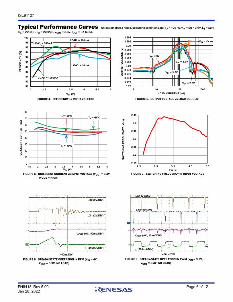
Typical Performance Curves Unless otherwise noted, operating conditions are: TA = +25°C, VIN = EN = 3.6V, L1 = 1µH, C1 = 2x10µF, C2 = 2x22µF, VOUT = 3.3V, IOUT = 0A to 3A.
FIGURE 4. EFFICIENCY vs INPUT VOLTAGE FIGURE 5. OUTPUT VOLTAGE vs LOAD CURRENT
FIGURE 6. QUIESCENT CURRENT vs INPUT VOLTAGE (VOUT = 3.3V, MODE = HIGH)
FIGURE 7. SWITCHING FREQUENCY vs INPUT VOLTAGE
FIGURE 8. STEADY-STATE OPERATION IN PFM (VIN = 4V, VOUT = 3.3V, NO LOAD)
FIGURE 9. STEADY-STATE OPERATION IN PWM (VIN = 3.3V, VOUT = 3.3V, NO LOAD)
80
82
84
86
88
90
92
94
96
98
100
2 2.5 3 3.5 4 4.5 5VIN (V)
LOAD = 10mA
LOAD = 100mALOAD = 500mA
LOAD = 1000mA
EFFI
CIE
NC
Y (%
)
3.273.2723.2743.2763.2783.28
3.2823.2843.2863.2883.29
3.2923.294
1 10 100 1000LOAD CURRENT (mA)
VIN = 3.3V
VIN = 4V
VI N = 2.5V
VIN = 3.6V
VIN = 3V
OU
TPU
T VO
LTA
GE
(V)
0
10
20
30
40
50
60
70
80
1.5 2 2.5 3 3.5 4 4.5 5 5.5 6
TA = +85oCTA = +25oC
TA = -40oC
VIN (V)
QU
IESC
ENT
CU
RR
ENT
(µA
)
2.15
2.2
2.25
2.3
2.35
2.4
2.45
1.5 2.5 3.5 4.5 5.5
SWIT
CH
ING
FR
EQU
ENC
Y (M
Hz)
VIN (V)
VOUT (AC, 50mV/DIV)
400ns/DIV
LX2 (2V/DIV)
LX1 (2V/DIV)
IL (500mA/DIV)
400ns/DIV
VOUT (AC, 10mV/DIV)
LX2 (2V/DIV)
LX1 (2V/DIV)
IL (200mA/DIV)
FN8418 Rev 5.00 Page 6 of 12Jan 28, 2022

ISL91127
FIGURE 10. SOFT-START (VIN = 3.6V, VOUT = 3.3V, NO LOAD) FIGURE 11. SOFT-START (VIN = 3.6V, VOUT = 3.3V, 1A LOAD)
FIGURE 12. STEADY-STATE OPERATION (VIN = 2.5V, VOUT = 3.3V,2A LOAD)
FIGURE 13. 0A TO 2A LOAD TRANSIENT (VIN = 3.6V, VOUT = 3.3V)
FIGURE 14. 0.5A TO 1.5A LOAD TRANSIENT (VIN = 3.6V, VOUT = 3.3V) FIGURE 15. 0A TO 1A LOAD TRANSIENT (VIN = 3.6V, VOUT = 3.3V)
Typical Performance Curves Unless otherwise noted, operating conditions are: TA = +25°C, VIN = EN = 3.6V, L1 = 1µH, C1 = 2x10µF, C2 = 2x22µF, VOUT = 3.3V, IOUT = 0A to 3A. (Continued)
400µs/DIV
VOUT (1V/DIV)
EN (2V/DIV)
IL (500mA/DIV)
400µs/DIV
VOUT (1V/DIV)
EN (2V/DIV)
IL (500mA/DIV)
VOUT (AC, 100mV/DIV)
400ns/DIV
LX2 (2V/DIV)
LX1 (2V/DIV)
IL (1A/DIV)
VOUT (AC, 100mV/DIV)
100µs/DIV
IL (1A/DIV)
VOUT (AC, 100mV/DIV)
100µs/DIV
IL (500mA/DIV)
VOUT (AC, 100mV/DIV)
100µs/DIV
IL (500mA/DIV)
FN8418 Rev 5.00 Page 7 of 12Jan 28, 2022
ISL91127
Functional DescriptionFunctional OverviewThe ISL91127 implements a complete buck-boost switching regulator with PWM controller, internal switches, references, protection circuitry, and control inputs. Refer to the “Block Diagram” on page 2
The PWM controller automatically switches between Buck and Boost modes as necessary to maintain a steady output voltage with changing input voltages and dynamic external loads.
Internal Supply and ReferencesReferring to the “Block Diagram”, the ISL91127 provides three PVIN power input pins. The PVIN pins supply input power to the DC/DC converter. An additional VIN pin provides an operating voltage source required for stable VREF generation. Separate ground pins (PGND and SGND) are provided to avoid problems caused by ground shift due to the high switching currents.
Enable InputEnable the device by asserting the EN pin HIGH. Driving EN LOW invokes a power-down mode, in which most internal device functions are disabled.
Soft DischargeWhen the device is disabled by driving EN LOW, an internal resistor between VOUT and GND is activated to slowly discharge the output capacitor. This internal resistor has a typical 120Ω resistance.
POR Sequence and Soft-StartAsserting the EN pin HIGH allows the device to power up. The following events occur during the start-up sequence: The internal voltage reference powers up and stabilizes. The device then starts operating. There is a typical 1ms delay between assertion of the EN pin and the start of the switching regulator soft-start ramp.
The soft-start feature minimizes output voltage overshoot and input inrush currents. During soft-start, the reference voltage is ramped to provide a ramping VOUT voltage. While the output voltage is lower than approximately 20% of the target output
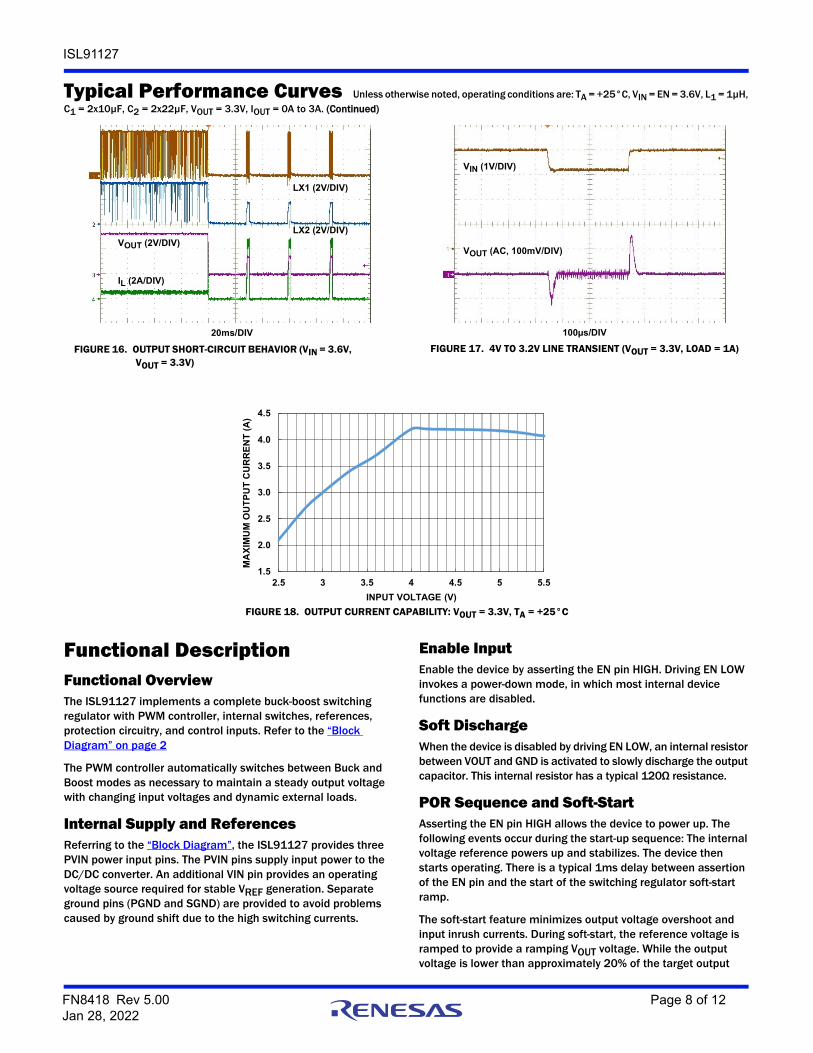
FIGURE 16. OUTPUT SHORT-CIRCUIT BEHAVIOR (VIN = 3.6V, VOUT = 3.3V)
FIGURE 17. 4V TO 3.2V LINE TRANSIENT (VOUT = 3.3V, LOAD = 1A)
FIGURE 18. OUTPUT CURRENT CAPABILITY: VOUT = 3.3V, TA = +25°C
Typical Performance Curves Unless otherwise noted, operating conditions are: TA = +25°C, VIN = EN = 3.6V, L1 = 1µH, C1 = 2x10µF, C2 = 2x22µF, VOUT = 3.3V, IOUT = 0A to 3A. (Continued)
VOUT (2V/DIV)LX2 (2V/DIV)
LX1 (2V/DIV)
IL (2A/DIV)
20ms/DIV
VOUT (AC, 100mV/DIV)
100µs/DIV
VIN (1V/DIV)
1.5
2.0
2.5
3.0
3.5
4.0
4.5
2.5 3 3.5 4 4.5 5 5.5INPUT VOLTAGE (V)
MA
XIM
UM
OU
TPU
T C
UR
REN
T (A
)
FN8418 Rev 5.00 Page 8 of 12Jan 28, 2022
ISL91127
voltage, switching frequency is reduced to a fraction of the normal switching frequency to aid in producing low duty cycles necessary to avoid input inrush current spikes. When the output voltage exceeds 20% of the target voltage, the switching frequency is increased to its nominal value.
When the target output voltage is higher than the input voltage, the device transitions from Buck mode to Boost mode during the soft-start sequence. At the time of this transition, the ramp rate of the reference voltage is decreased, such that the output voltage slew rate is decreased. This provides a slower output voltage slew rate.
The VOUT ramp time is not constant for all operating conditions. Soft-start into Boost mode takes longer than soft-start into Buck mode. The total soft-start time into Buck operating mode is typically 2ms, whereas the typical soft-start time into Boost operating mode is typically 3ms. Increasing the load current increases these typical soft-start times.
Short-Circuit ProtectionThe ISL91127 provides short-circuit protection by monitoring the feedback voltage. When feedback voltage is sensed to be lower than a certain threshold, the PWM oscillator frequency is reduced in order to protect the device from damage. The P-channel MOSFET peak current limit remains active during this state.
Thermal ShutdownA built-in thermal protection feature protects the ISL91127 if the die temperature reaches +155°C (typical). At this die temperature, the regulator is completely shut down. The die temperature continues to be monitored in this thermal shutdown mode. When the die temperature falls to +125°C (typical), the device will resume normal operation. When exiting thermal shutdown, the ISL91127 will execute its soft-start sequence.
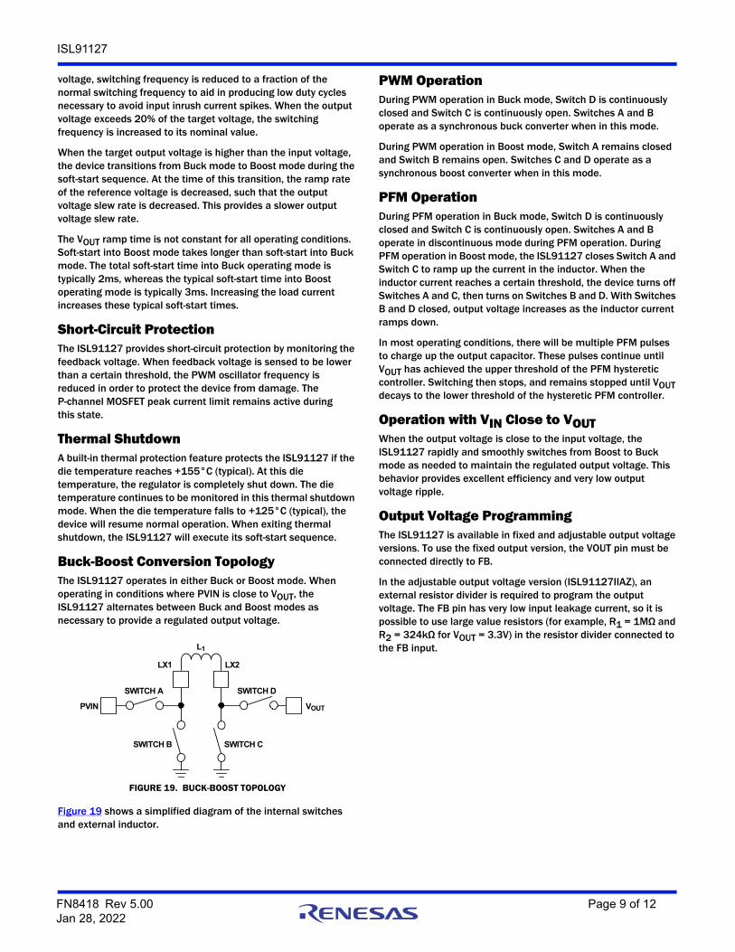
Buck-Boost Conversion TopologyThe ISL91127 operates in either Buck or Boost mode. When operating in conditions where PVIN is close to VOUT, the ISL91127 alternates between Buck and Boost modes as necessary to provide a regulated output voltage.
Figure 19 shows a simplified diagram of the internal switches and external inductor.
PWM OperationDuring PWM operation in Buck mode, Switch D is continuously closed and Switch C is continuously open. Switches A and B operate as a synchronous buck converter when in this mode.
During PWM operation in Boost mode, Switch A remains closed and Switch B remains open. Switches C and D operate as a synchronous boost converter when in this mode.
PFM OperationDuring PFM operation in Buck mode, Switch D is continuously closed and Switch C is continuously open. Switches A and B operate in discontinuous mode during PFM operation. During PFM operation in Boost mode, the ISL91127 closes Switch A and Switch C to ramp up the current in the inductor. When the inductor current reaches a certain threshold, the device turns off Switches A and C, then turns on Switches B and D. With Switches B and D closed, output voltage increases as the inductor current ramps down.
In most operating conditions, there will be multiple PFM pulses to charge up the output capacitor. These pulses continue until VOUT has achieved the upper threshold of the PFM hysteretic controller. Switching then stops, and remains stopped until VOUT decays to the lower threshold of the hysteretic PFM controller.
Operation with VIN Close to VOUTWhen the output voltage is close to the input voltage, the ISL91127 rapidly and smoothly switches from Boost to Buck mode as needed to maintain the regulated output voltage. This behavior provides excellent efficiency and very low output voltage ripple.
Output Voltage ProgrammingThe ISL91127 is available in fixed and adjustable output voltage versions. To use the fixed output version, the VOUT pin must be connected directly to FB.
In the adjustable output voltage version (ISL91127IIAZ), an external resistor divider is required to program the output voltage. The FB pin has very low input leakage current, so it is possible to use large value resistors (for example, R1 = 1MΩ and R2 = 324kΩ for VOUT = 3.3V) in the resistor divider connected to the FB input.
FIGURE 19. BUCK-BOOST TOPOLOGY
PVIN VOUT
SWITCH A SWITCH D
SWITCH B SWITCH C
LX1 LX2
L1
FN8418 Rev 5.00 Page 9 of 12Jan 28, 2022

ISL91127
Applications InformationComponent SelectionThe fixed-output version of the ISL91127 requires only three external power components to implement the buck-boost converter: an inductor, an input capacitor, and an output capacitor.
The adjustable output version of the ISL91127 requires three additional components to program the output voltage, as shown in Figure 19. Two external resistors program the output voltage and a small capacitor is added to improve stability and response..
Output Voltage Programming, Adjustable VersionWhen VREF is connected to GND, select the external resistor values to set and control the output voltage of the ISL91127IIAZ (adjustable output version).
Equation 1 can be used to derive the R1 and R2 resistor values:
When designing a PCB, include a GND guard band around the feedback resistor network to reduce noise and improve accuracy and stability. Position resistors R1 and R2 close to the FB pin.
Feed-Forward Capacitor Selection A small capacitor (C3 in Figure 19) in parallel with resistor R1 is required to provide the specified load and line regulation. The suggested value of this capacitor is 56pF for R1 = 1MΩ. An NPO type capacitor is recommended.
Inductor SelectionUse an inductor with high frequency core material (for example, ferrite core) to minimize core losses and provide good efficiency. The inductor must be able to handle the peak switching currents without saturating.
A 1µH inductor with ≥4A saturation current rating is recommended. Select an inductor with low DCR to provide good efficiency. In applications where radiated noise must be minimized, a toroidal or shielded inductor can be used (refer to Table 3).
PVIN and VOUT Capacitor Selection The input and output capacitors should be ceramic X5R type with low ESL and ESR. The recommended input capacitor value is 10µF. The recommended VOUT capacitor value is 2x22µF.
Recommended PCB LayoutCorrect PCB layout is critical for proper operation of the ISL91127. Place the input and output capacitors as close to the IC as possible. The ground connections of the input and output capacitors should be kept as short as possible and should be on the component layer to avoid problems that are caused by high switching currents flowing through PCB vias.
FIGURE 20. ADJUSTABLE OUTPUT APPLICATION
PVINVIN = 1.8V TO 5.5V
VOUT = 1V TO
ISL91127IIAZ
VIN
EN
LX1
LX2
VOUT
FB
SGN
D
PGN
D
C110µF
L11µH
C22x22µF
MODER1
R2
C3
VOUT 0.8V 1R1R2-------+
•= (EQ. 1)
TABLE 2. CAPACITOR VENDOR INFORMATION
MANUFACTURER PN DESCRIPTION
Murata GRM188R61A226ME15D 22µF, 0603, 10V, X5R
TDK C1608X5R1A226M080AC 22µF, 0603, 10V, X5R
TABLE 3. INDUCTOR VENDOR INFORMATION
MANUFACTURERMANUFACTURERPART NUMBER DESCRIPTION
DIMENSION(mm) WEBSITE
Toko 1277AS-H-1R0M 1µH, 20%, DCR = 34mΩ (typical), ISAT = 4.6A (typical) 3.2x2.5x1.2 www.toko.com
FDSD0312-H-1R0M 1µH, 20%, DCR = 43mΩ (typical), ISAT = 4.5A (typical) 3.2x3.0x1.2
Coilcraft XFL4020-102ME 1µH, 20%, DCR = 11mΩ (typical), ISAT = 5.1A (typical) 4.0x4.0x2.1 www.coilcraft.com
FN8418 Rev 5.00 Page 10 of 12Jan 28, 2022
ISL91127
Revision History The revision history provided is for informational purposes only and is believed to be accurate, however, not warranted. Please visit to web to make sure you have the latest revision.
DATE REVISION CHANGE
Jan 28, 2022 FN8418.5 Updated Figure 3: Removed the resistive connection between EN and SGND.Removed Related Literature.
May 24, 2018 FN8418.4 Removed About Intersil section.Updated Disclaimer and moved to page 13.
Jan 5, 2017 FN8418.3 Updated Related Literature section on page 1.Updated Table 1 on page 3.- changed “VSEL” column to “Dynamic Voltage Scaling” and made ISL91128 parameter “Yes”.- removed “and DVS” from I2C column.
Aug 9, 2016 FN8418.2 Removed burst current features bullet on page 1.Updated Table 1 on page 3.Removed “VIN = 3.0V VOUT = 3.3V, tON = 600µs, t = 4.6ms...3A” from the “Recommended Operating Conditions” on page 4.
Jul 15, 2016 FN8418.1 Updated 2 feature bullets to clarify statement.Updated Table 1 on page 3.Updated test conditions for VIN supply current page 4 from “PFM mode, no external load on VOUT” to “PFM mode, 1.8V ≤ VIN ≤ 5V, no external load on”.Updated “P-Channel MOSFET ON-Resistance” typical from 35 to 28 and “N-Channel MOSFET ON-Resistance” typical from 24 to 26 typical.Added Figure 18, “OUTPUT CURRENT CAPABILITY” to typical Performance Curves” on page 8.
Apr 5, 2016 FN8418.0 Initial Release
FN8418 Rev 5.00 Page 11 of 12Jan 28, 2022
ISL91127
FN8418 Rev 5.00 Page 12 of 12Jan 28, 2022
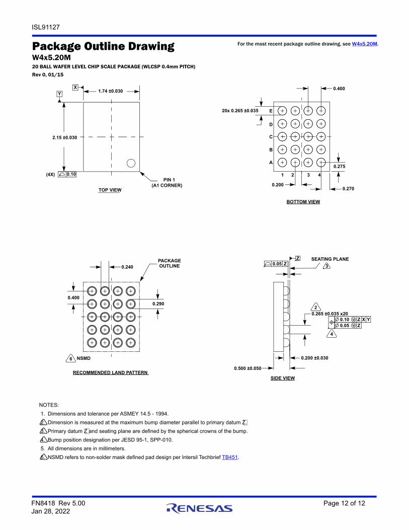
Package Outline DrawingW4x5.20M20 BALL WAFER LEVEL CHIP SCALE PACKAGE (WLCSP 0.4mm PITCH)
Rev 0, 01/15
BOTTOM VIEW
20x 0.265 ±0.035
1 2 3 4
RECOMMENDED LAND PATTERN
PIN 1 (A1 CORNER)
1.74 ±0.030
2.15 ±0.030
XY
0.10(4X)
TOP VIEW
0.275
0.2700.200
0.400
A
B
C
D
E
0.240
0.400
PACKAGEOUTLINE
0.290
6 NSMD
SIDE VIEW
0.200 ±0.030
0.500 ±0.050
0.10 Z X Y0.05 Z
0.265 ±0.035 x202
4
SEATING PLANEZ0.05 Z 3
NOTES:1. Dimensions and tolerance per ASMEY 14.5 - 1994.2. Dimension is measured at the maximum bump diameter parallel to primary datum Z.3. Primary datum Z and seating plane are defined by the spherical crowns of the bump.4. Bump position designation per JESD 95-1, SPP-010.5. All dimensions are in millimeters.6. NSMD refers to non-solder mask defined pad design per Intersil Techbrief TB451.
For the most recent package outline drawing, see W4x5.20M.
Corporate HeadquartersTOYOSU FORESIA, 3-2-24 Toyosu,Koto-ku, Tokyo 135-0061, Japanwww.renesas.com
Contact InformationFor further information on a product, technology, the most up-to-date version of a document, or your nearest sales office, please visit:www.renesas.com/contact/
TrademarksRenesas and the Renesas logo are trademarks of Renesas Electronics Corporation. All trademarks and registered trademarks are the property of their respective owners.
IMPORTANT NOTICE AND DISCLAIMER
RENESAS ELECTRONICS CORPORATION AND ITS SUBSIDIARIES (“RENESAS”) PROVIDES TECHNICAL SPECIFICATIONS AND RELIABILITY DATA (INCLUDING DATASHEETS), DESIGN RESOURCES (INCLUDING REFERENCE DESIGNS), APPLICATION OR OTHER DESIGN ADVICE, WEB TOOLS, SAFETY INFORMATION, AND OTHER RESOURCES “AS IS” AND WITH ALL FAULTS, AND DISCLAIMS ALL WARRANTIES, EXPRESS OR IMPLIED, INCLUDING, WITHOUT LIMITATION, ANY IMPLIED WARRANTIES OF MERCHANTABILITY, FITNESS FOR A PARTICULAR PURPOSE, OR NON-INFRINGEMENT OF THIRD PARTY INTELLECTUAL PROPERTY RIGHTS.
These resources are intended for developers skilled in the art designing with Renesas products. You are solely responsible for (1) selecting the appropriate products for your application, (2) designing, validating, and testing your application, and (3) ensuring your application meets applicable standards, and any other safety, security, or other requirements. These resources are subject to change without notice. Renesas grants you permission to use these resources only for development of an application that uses Renesas products. Other reproduction or use of these resources is strictly prohibited. No license is granted to any other Renesas intellectual property or to any third party intellectual property. Renesas disclaims responsibility for, and you will fully indemnify Renesas and its representatives against, any claims, damages, costs, losses, or liabilities arising out of your use of these resources. Renesas' products are provided only subject to Renesas' Terms and Conditions of Sale or other applicable terms agreed to in writing. No use of any Renesas resources expands or otherwise alters any applicable warranties or warranty disclaimers for these products.
(Rev.1.0 Mar 2020)