Embed Size (px)
Citation preview

FN7938Rev 1.00
April 23, 2015
ISL94212Multi-Cell Li-Ion Battery Manager
DATASHEET
The ISL94212 Li-ion battery manager IC supervises up to 12 series connected cells. The part provides accurate monitoring, cell balancing and extensive system diagnostics functions. Three cell balancing modes are provided: Manual Balancing mode, Timed Balancing mode and Auto Balance mode. The Auto Balance mode terminates balancing functions when a charge transfer value has been met.
The ISL94212 communicates to a host microcontroller via an SPI interface and to other ISL94212 devices using a robust, proprietary, two-wire Daisy Chain system.
The ISL94212 is offered in a 64 Ld TQFP package and is specified for an operational temperature range of -40°C to +85°C.
Applications• Light electric vehicle (LEV); E-Moto; E-Bike
• Battery backup systems; Energy Storage Systems (ESS)
• Solar Farms
• Portable and semi-portable equipment
Features• Up to 12-cell voltage monitors, support Li-Ion CoO2, Li-ion
Mn2O4, and Li-ion FePO4 chemistries
• Cell voltage measurement accuracy ±10mV
• 13-bit cell voltage measurement
• Pack voltage measurement accuracy ±180mV
• 14-bit pack voltage and temperature measurements
• Cell voltage scan rate of 19.5µs per cell (234µs to scan 12 cells)
• Internal temperature monitoring
• Up to four external temperature inputs
• Robust daisy chain communications system
• Integrated system diagnostics for all key internal functions
• Hardwired and communications based fault notification
• Integrated watchdog shuts down device if communication is lost
• 7µA shutdown current: Enable = VSS
• 2Mbps SPI
ISL94212
DHi2
DLo2
SCLK
DOUTDIN
CSHOST
DATA READY
FAULT
TO OTHER DEVICES (OPTIONAL)
EN
MONITOR BOARD (Master or Standalone)
MICRO
ISL94212
DHi1
DLo1
MONITOR BOARD (Daisy Chain - Optional)
DHi2
DLo2
VG1 VG1
VG1 VG1 VG2
VG2 VG2
FIGURE 1. TYPICAL APPLICATION
FN7938 Rev 1.00 Page 1 of 96April 23, 2015

ISL94212
Table of ContentsOrdering Information . . . . . . . . . . . . . . . . . . . . . . . . . . . . . . . . 4
Pin Configuration. . . . . . . . . . . . . . . . . . . . . . . . . . . . . . . . . . . . 4
Absolute Maximum Ratings . . . . . . . . . . . . . . . . . . . . . . . . . . . 7
Thermal Information . . . . . . . . . . . . . . . . . . . . . . . . . . . . . . . . . 7
Recommended Operating Conditions . . . . . . . . . . . . . . . . . . 7
Electrical Specifications . . . . . . . . . . . . . . . . . . . . . . . . . . . . . 7
Timing Diagrams . . . . . . . . . . . . . . . . . . . . . . . . . . . . . . . . . . .14
Typical Performance Curves . . . . . . . . . . . . . . . . . . . . . . . . .15
Device Description and Operation . . . . . . . . . . . . . . . . . . . .21
Power Modes . . . . . . . . . . . . . . . . . . . . . . . . . . . . . . . . . . . . . .21
Measurement Modes. . . . . . . . . . . . . . . . . . . . . . . . . . . . . . . .21
Measurement Mode Commands . . . . . . . . . . . . . . . . . . . . . .21
Scan Once . . . . . . . . . . . . . . . . . . . . . . . . . . . . . . . . . . . . . . . . .22
Scan Voltages. . . . . . . . . . . . . . . . . . . . . . . . . . . . . . . . . . . . . . . 22
Scan Temperatures . . . . . . . . . . . . . . . . . . . . . . . . . . . . . . . . . . 22
Scan Mixed . . . . . . . . . . . . . . . . . . . . . . . . . . . . . . . . . . . . . . . . . 22
Scan Wires . . . . . . . . . . . . . . . . . . . . . . . . . . . . . . . . . . . . . . . . . 22
Scan All . . . . . . . . . . . . . . . . . . . . . . . . . . . . . . . . . . . . . . . . . . . . 22
Scan Continuous . . . . . . . . . . . . . . . . . . . . . . . . . . . . . . . . . . .23
Measure. . . . . . . . . . . . . . . . . . . . . . . . . . . . . . . . . . . . . . . . . . .23
Cell Voltage Measurement Accuracy . . . . . . . . . . . . . . . . . .24
Temperature Monitoring . . . . . . . . . . . . . . . . . . . . . . . . . . . . .24
Cell Balancing Functions . . . . . . . . . . . . . . . . . . . . . . . . . . . .25
Balance Setup Register . . . . . . . . . . . . . . . . . . . . . . . . . . . . . . 25
Balance Status Register . . . . . . . . . . . . . . . . . . . . . . . . . . . . . . 26
Manual Balance Mode . . . . . . . . . . . . . . . . . . . . . . . . . . . . . . . 26
Timed Balance Mode. . . . . . . . . . . . . . . . . . . . . . . . . . . . . . . . . 27
Auto Balance Mode . . . . . . . . . . . . . . . . . . . . . . . . . . . . . . . . . . 27
Balance FET Drivers. . . . . . . . . . . . . . . . . . . . . . . . . . . . . . . . . . 29
Device Setup Register . . . . . . . . . . . . . . . . . . . . . . . . . . . . . . . . 30
Cell Balance Enabled Register . . . . . . . . . . . . . . . . . . . . . . . . . 30
System Configuration . . . . . . . . . . . . . . . . . . . . . . . . . . . . . . .31
SPI Interface. . . . . . . . . . . . . . . . . . . . . . . . . . . . . . . . . . . . . . .31
Full Duplex Operation . . . . . . . . . . . . . . . . . . . . . . . . . . . . . . . . 31
Half Duplex Operation . . . . . . . . . . . . . . . . . . . . . . . . . . . . . . . . 32
Non-daisy Chain Systems . . . . . . . . . . . . . . . . . . . . . . . . . . . .33
Normal Communications . . . . . . . . . . . . . . . . . . . . . . . . . . . . . 33
Alarm Signals . . . . . . . . . . . . . . . . . . . . . . . . . . . . . . . . . . . . . . . 33
Communication Faults . . . . . . . . . . . . . . . . . . . . . . . . . . . . . . . 33
Fault Response in Sleep Mode. . . . . . . . . . . . . . . . . . . . . . . . . 34
Example Communications . . . . . . . . . . . . . . . . . . . . . . . . . . . . 34
Daisy Chain Systems. . . . . . . . . . . . . . . . . . . . . . . . . . . . . . . .34
Daisy Chain Ports. . . . . . . . . . . . . . . . . . . . . . . . . . . . . . . . . . . . 34
Communications Protocol . . . . . . . . . . . . . . . . . . . . . . . . . . . . 35
Communication Sequences . . . . . . . . . . . . . . . . . . . . . . . . . . . 36
CRC Calculation . . . . . . . . . . . . . . . . . . . . . . . . . . . . . . . . . . . . 36
Daisy Chain Addressing . . . . . . . . . . . . . . . . . . . . . . . . . . . . . . 38
Daisy Chain Commands . . . . . . . . . . . . . . . . . . . . . . . . . . . . . 40
Identify . . . . . . . . . . . . . . . . . . . . . . . . . . . . . . . . . . . . . . . . . . . . 40
ACK (Acknowledge) . . . . . . . . . . . . . . . . . . . . . . . . . . . . . . . . . 42
NAK (Not Acknowledge). . . . . . . . . . . . . . . . . . . . . . . . . . . . . . 42
Reset . . . . . . . . . . . . . . . . . . . . . . . . . . . . . . . . . . . . . . . . . . . . . 42
Address All. . . . . . . . . . . . . . . . . . . . . . . . . . . . . . . . . . . . . . . . . 42
Alarm Signals . . . . . . . . . . . . . . . . . . . . . . . . . . . . . . . . . . . . . 43
Watchdog Function. . . . . . . . . . . . . . . . . . . . . . . . . . . . . . . . . 43
Communications Faults . . . . . . . . . . . . . . . . . . . . . . . . . . . . . 44
Communication Failure . . . . . . . . . . . . . . . . . . . . . . . . . . . . . . 44
Scan Counter . . . . . . . . . . . . . . . . . . . . . . . . . . . . . . . . . . . . . . . 45
Daisy Chain Communications Conflicts . . . . . . . . . . . . . . . . 45
Memory Checksum . . . . . . . . . . . . . . . . . . . . . . . . . . . . . . . . . 45
Settling Time Following Diagnostic Activity . . . . . . . . . . . . 45
Open Wire Test . . . . . . . . . . . . . . . . . . . . . . . . . . . . . . . . . . . . . 45
Cell Balancing . . . . . . . . . . . . . . . . . . . . . . . . . . . . . . . . . . . . . . 45
Fault Signal Filtering . . . . . . . . . . . . . . . . . . . . . . . . . . . . . . . 46
Fault Diagnostics . . . . . . . . . . . . . . . . . . . . . . . . . . . . . . . . . . 46
Sleep Mode . . . . . . . . . . . . . . . . . . . . . . . . . . . . . . . . . . . . . . . 50
Wakeup . . . . . . . . . . . . . . . . . . . . . . . . . . . . . . . . . . . . . . . . . . . 50
Fault Response in Sleep Mode . . . . . . . . . . . . . . . . . . . . . . . . 50
Communication and Measurement Diagrams . . . . . . . . . . 50
Measurement Timing Diagrams . . . . . . . . . . . . . . . . . . . . . . . 51
Command Timing Diagram . . . . . . . . . . . . . . . . . . . . . . . . . . . 52
Response Timing Diagrams . . . . . . . . . . . . . . . . . . . . . . . . . . 53
Communication and Measurement Timing Tables . . . . . . 56
Measurement Timing Tables. . . . . . . . . . . . . . . . . . . . . . . . . . 56
Command Timing Tables. . . . . . . . . . . . . . . . . . . . . . . . . . . . . 57
Response Timing Tables . . . . . . . . . . . . . . . . . . . . . . . . . . . . . 58
System Registers . . . . . . . . . . . . . . . . . . . . . . . . . . . . . . . . . . 62
Register Descriptions . . . . . . . . . . . . . . . . . . . . . . . . . . . . . . 62
Cell Voltage Data . . . . . . . . . . . . . . . . . . . . . . . . . . . . . . . . . . . 62
Temperature Data, Secondary Voltage ReferenceData, Scan Count . . . . . . . . . . . . . . . . . . . . . . . . . . . . . . . . . 62
Fault Registers . . . . . . . . . . . . . . . . . . . . . . . . . . . . . . . . . . . . . 63
Setup Registers. . . . . . . . . . . . . . . . . . . . . . . . . . . . . . . . . . . . . 66
Cell Balance Registers . . . . . . . . . . . . . . . . . . . . . . . . . . . . . . . 69
Reference Coefficient Registers . . . . . . . . . . . . . . . . . . . . . . . 69
Cells In Balance Register . . . . . . . . . . . . . . . . . . . . . . . . . . . . . 70
Device Commands . . . . . . . . . . . . . . . . . . . . . . . . . . . . . . . . . . 70
Nonvolatile Memory (EEPROM) Checksum . . . . . . . . . . . . . . 71
Applications Circuits Information . . . . . . . . . . . . . . . . . . . . 72
Typical Applications Circuits . . . . . . . . . . . . . . . . . . . . . . . . . . 72
Typical Application Circuits. . . . . . . . . . . . . . . . . . . . . . . . . . 73
Notes on Board Layout . . . . . . . . . . . . . . . . . . . . . . . . . . . . . 77
FN7938 Rev 1.00 Page 2 of 96April 23, 2015

ISL94212
Component Selection . . . . . . . . . . . . . . . . . . . . . . . . . . . . . . . . 78
Operating the ISL94212 with Reduced Cell Counts . . . . . . . 78
Typical Application Circuits . . . . . . . . . . . . . . . . . . . . . . . . . .79
Power Supplies . . . . . . . . . . . . . . . . . . . . . . . . . . . . . . . . . . . . . 82
Voltage Reference Bypass Capacitor . . . . . . . . . . . . . . . . . . . 82
Cell Balancing Circuits. . . . . . . . . . . . . . . . . . . . . . . . . . . . . . . . 82
Cell Voltage Measurements During Balancing. . . . . . . . . . . . 83
Balancing with Scan Continuous Mode Enabled . . . . . . . . . . 83
Daisy Chain Communications System . . . . . . . . . . . . . . . . . . 83
External Inputs . . . . . . . . . . . . . . . . . . . . . . . . . . . . . . . . . . . . . . 85
Board Level Calibration. . . . . . . . . . . . . . . . . . . . . . . . . . . . . . . 86
Worked Examples . . . . . . . . . . . . . . . . . . . . . . . . . . . . . . . . . .86
Voltage Reference Check Calculation. . . . . . . . . . . . . . . . . . . 86
Cell Balancing – Manual Mode . . . . . . . . . . . . . . . . . . . . . . . . 87
Cell Balancing – Timed Mode . . . . . . . . . . . . . . . . . . . . . . . . . 87
Cell Balancing – Auto Mode . . . . . . . . . . . . . . . . . . . . . . . . . . . 88
Register Map . . . . . . . . . . . . . . . . . . . . . . . . . . . . . . . . . . . . . .90
Revision History. . . . . . . . . . . . . . . . . . . . . . . . . . . . . . . . . . . .95
Package Outline Drawing . . . . . . . . . . . . . . . . . . . . . . . . . . . .96
FN7938 Rev 1.00 Page 3 of 96April 23, 2015
ISL94212
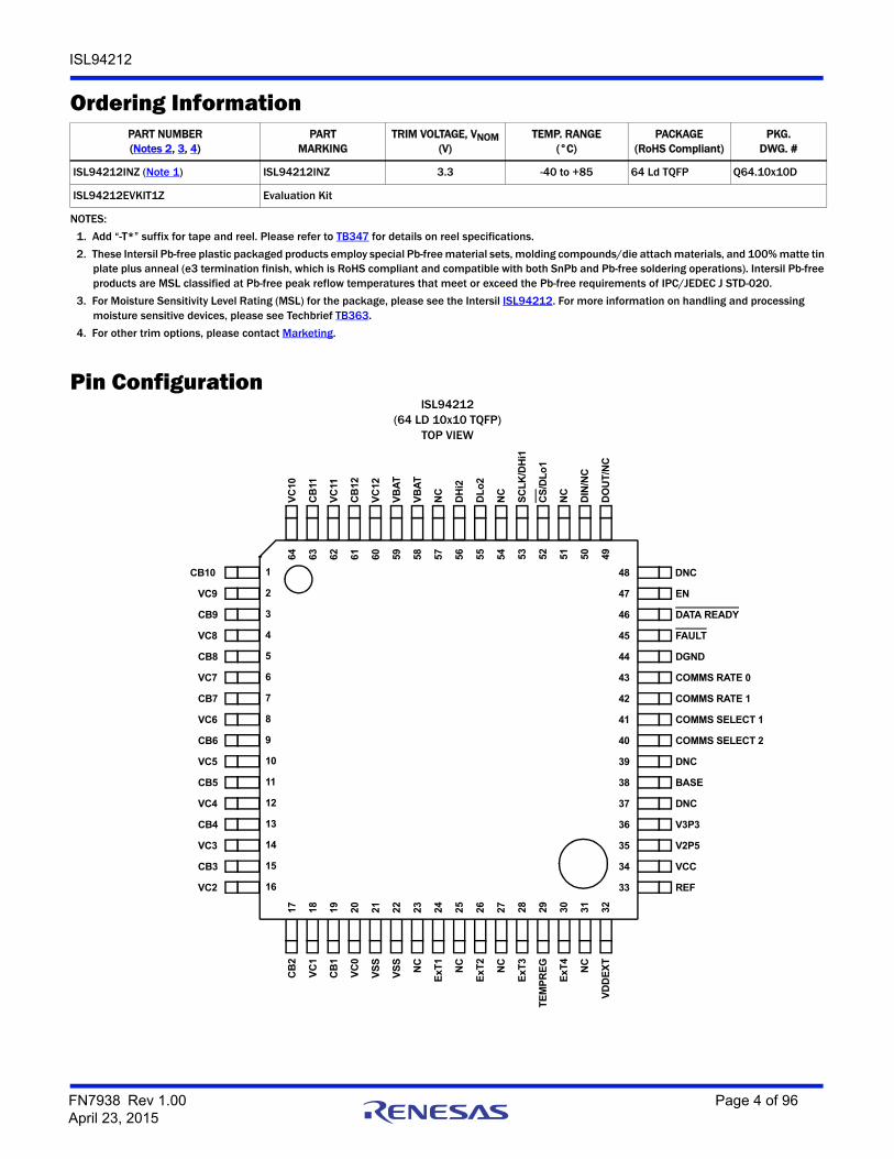
Pin ConfigurationISL94212
(64 LD 10x10 TQFP)TOP VIEW
Ordering Information PART NUMBER(Notes 2, 3, 4)
PARTMARKING
TRIM VOLTAGE, VNOM (V)
TEMP. RANGE(°C)
PACKAGE(RoHS Compliant)
PKG. DWG. #
ISL94212INZ (Note 1) ISL94212INZ 3.3 -40 to +85 64 Ld TQFP Q64.10x10D
ISL94212EVKIT1Z Evaluation Kit
NOTES:
1. Add “-T*” suffix for tape and reel. Please refer to TB347 for details on reel specifications.
2. These Intersil Pb-free plastic packaged products employ special Pb-free material sets, molding compounds/die attach materials, and 100% matte tin plate plus anneal (e3 termination finish, which is RoHS compliant and compatible with both SnPb and Pb-free soldering operations). Intersil Pb-free products are MSL classified at Pb-free peak reflow temperatures that meet or exceed the Pb-free requirements of IPC/JEDEC J STD-020.
3. For Moisture Sensitivity Level Rating (MSL) for the package, please see the Intersil ISL94212. For more information on handling and processing moisture sensitive devices, please see Techbrief TB363.
4. For other trim options, please contact Marketing.
DATA READY
FAULT
DGND
COMMS SELECT 1
COMMS SELECT 2
DNC
BASE
DNC
V3P3
CB10
VC9
CB9
VC8
CB8
VC7
CB7
VC6
CB
2
VC
1
CB
1
VC
0
VS
S
VS
S
NC
ExT
2
CB
12
VC
12
VB
AT
VB
AT
NC
DH
i2
DL
o2
NC
ExT
1
NC
NC
CB6
VC5
CB5
VC
10
CB
11
VC
11
EN
VC4
CB4
VC3
CB3
VC2
ExT
3
NC
TE
MP
RE
G
ExT
4
VD
DE
XT
SC
LK
/DH
i1
CS
/DL
o1
NC
DIN
/NC
DO
UT
/NC
V2P5
VCC
COMMS RATE 0
COMMS RATE 1
REF
DNC48
47
46
45
44
43
42
41
40
39
38
1
2
3
4
5
6
7
8
9
10
11
17 18 19 20 21 22 23 24 25 26 27
64 63 62 61 60 59 58 57 56 55 54
12
13
14
15
16
28 29 30 31 32
53 52 51 50 49
37
36
35
34
33
FN7938 Rev 1.00 Page 4 of 96April 23, 2015

ISL94212
Pin DescriptionsSYMBOL PIN NUMBER DESCRIPTION
VC0, VC1, VC2, VC3, VC4, VC5, VC6, VC7, VC8, VC9,
VC10, VC11, VC12
20, 18, 16, 14, 12, 10, 8,
6, 4, 2, 64, 62, 60
Battery cell voltage inputs. VCn connects to the positive terminal of CELLn and the negative terminal of CELLn+1. (VC12 connects only to the positive terminal of CELL12 and VC0 only connects with the negative terminal of CELL1.)
CB1, CB2, CB3, CB4, CB5, CB6, CB7, CB8, CB9, CB10,
CB11, CB12
19, 17, 15, 13, 11, 9, 7,
5, 3, 1, 63, 61
Cell Balancing FET control outputs. Each output controls an external FET which provides a current path around the cell for balancing.
VBAT 58, 59 Main IC Supply pins. Connect to the most positive terminal in the battery string.
VSS 21, 22 Ground. These pins connect to the most negative terminal in the battery string.
ExT1, ExT2, ExT3, ExT4 24, 26, 28, 30
External temperature monitor or general purpose inputs. The temperature inputs are intended for use with external resistor networks using NTC type thermistor sense elements but may also be used as general purpose analog inputs at the user’s discretion. 0V to 2.5V input range.
TEMPREG 29 Temperature monitor voltage regulator output. This is a switched 2.5V output, which supplies a reference voltage to external NTC thermistor circuits to provide ratiometric ADC inputs for temperature measurement.
VDDEXT 32 External V3P3 supply input/output. Connected to the V3P3 pin via a switch, this pin may be used to power external circuits from the V3P3 supply. The switch is open when the ISL94212 is placed in Sleep mode.
REF 33 2.5V voltage reference decoupling pin. Connect a 2.0µF to 2.5µF X7R capacitor to VSS. Do not connect any additional external load to this pin.
VCC 34 Analog supply voltage input. Connect to V3P3 via a 33Ω resistor. Connect a 1µF capacitor to ground.
V2P5 35 Internal 2.5V digital supply decoupling pin. Connect a 1µF capacitor to DGND.
V3P3 36 3.3V digital supply voltage input. Connect the emitter of the external NPN regulator transistor to this pin. Connect a 1µF capacitor to DGND.
Base 38 Regulator control pin. Connect the external NPN transistor’s base. Do not let this pin float,
DNC 37, 39, 48 Do not connect. Leave pins floating.
Comms Select 1 41 Communications port 1 mode select pin. Connect via a 1kΩ resistor to V3P3 for Daisy Chain communications on port 1 or to DGND for SPI operation on port 1.
Comms Select 2 40 Communications port 2 mode select pin. Connect via a 1kΩ resistor to V3P3 to enable port 2 or to DGND to disable this port.
Comms Rate 0, Comms Rate 1
43, 42 Daisy Chain communications data rate setting. Connect via a 1kΩ resistor to DGND (‘0’) or to V3P3 (‘1’) to select between various communication data rates.
DGND 44 Digital Ground.
Fault 45 Logic fault output. Asserted low if a fault condition exists.
Data Ready 46 SPI data ready. Asserted low when the device is ready to transmit data to the host microcontroller.
EN 47 Enable input. Tie to V3P3 to enable the part. Tie to DGND to disable (all IC functions are turned off).
DOUT/NC 49 Serial Data Output (SPI) orNC (Daisy Chain). 0V to 3.3V push-pull output.
DIN/NC 50 Serial Data Input (SPI) orNC (Daisy Chain). 0V to 3.3V input.
CS/DLo1 52 Chip-Select, active low 3.3V input (SPI) orDaisy Chain port 1 Lo connection.
SCLK/DHi1 53 Serial-Clock Input (SPI) orDaisy Chain port 1 Hi connection.
DHi2 56 Daisy Chain port 2 Hi connection.
DLo2 55 Daisy Chain port 2 Lo connection.
NC 23, 25, 27, 31, 51, 54,
57
No internal connection.
FN7938 Rev 1.00 Page 5 of 96April 23, 2015
ISL94212
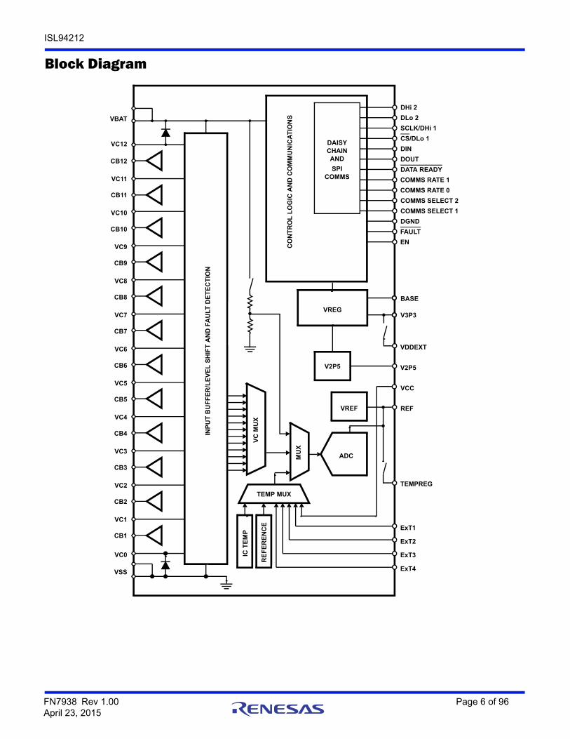
Block Diagram
VC12
INP
UT
BU
FF
ER
/LE
VE
L S
HIF
T A
ND
FA
ULT
DE
TE
CT
ION
DHi 2
VC
MU
X
ADC
TEMP MUX
IC T
EM
P
MU
X
SCLK/DHi 1
CS/DLo 1
DIN
DOUT
DLo 2
COMMS SELECT 2
CO
NT
RO
L L
OG
IC A
ND
CO
MM
UN
ICA
TIO
NS
DAISY
AND
SPICOMMS
TEMPREG
DATA READY
V3P3
CB12
VC11
ExT1
ExT2
ExT3
ExT4
DGND
COMMS SELECT 1
VBAT
VSS
CB11
VC10
CB10
VC9
CB9
VC8
CB8
VC7
CB7
VC6
CB6
VC5
CB5
VC4
CB4
VC3
CB3
VC2
CB2
VC1
CB1
VC0
VREG
REFVREF
EN
COMMS RATE 1
COMMS RATE 0
BASE
FAULT
VCC
VDDEXT
V2P5 V2P5
RE
FE
RE
NC
E
CHAIN
FN7938 Rev 1.00 Page 6 of 96April 23, 2015

ISL94212
Absolute Maximum Ratings Thermal InformationUnless otherwise specified. With respect to VSS.
DIN, SCLK, CS, DOUT, Data Ready, Comms Select n, ExTn, TEMPREG, REF, V3P3, VCC, Fault, Comms Rate n, Base, EN, VDDEXT. . . . . . . . . . . . . . . . . . . . . . .-0.2V to 4.1VV2P5. . . . . . . . . . . . . . . . . . . . . . . . . . . . . . . . . . . . . . . . . . . . . . . -0.2V to 2.9VVBAT . . . . . . . . . . . . . . . . . . . . . . . . . . . . . . . . . . . . . . . . . . . . . . . . -0.5V to 63VDhi1, DLo1, DHi2, DLo2 . . . . . . . . . . . . . . . . . . . . . . . -0.5V to (VBAT + 0.5V)VC0 . . . . . . . . . . . . . . . . . . . . . . . . . . . . . . . . . . . . . . . . . . . . . . . -0.5V to + 9.0VVC1 . . . . . . . . . . . . . . . . . . . . . . . . . . . . . . . . . . . . . . . . . . . . . . . -0.5V to + 18VVC2 . . . . . . . . . . . . . . . . . . . . . . . . . . . . . . . . . . . . . . . . . . . . . . . -0.5V to + 18VVC3 . . . . . . . . . . . . . . . . . . . . . . . . . . . . . . . . . . . . . . . . . . . . . . . -0.5V to + 27VVC4 . . . . . . . . . . . . . . . . . . . . . . . . . . . . . . . . . . . . . . . . . . . . . . . -0.5V to + 27VVC5 . . . . . . . . . . . . . . . . . . . . . . . . . . . . . . . . . . . . . . . . . . . . . . . -0.5V to + 36VVC6 . . . . . . . . . . . . . . . . . . . . . . . . . . . . . . . . . . . . . . . . . . . . . . . -0.5V to + 36VVC7 . . . . . . . . . . . . . . . . . . . . . . . . . . . . . . . . . . . . . . . . . . . . . . . -0.5V to + 45VVC8 . . . . . . . . . . . . . . . . . . . . . . . . . . . . . . . . . . . . . . . . . . . . . . . -0.5V to + 45VVC9 . . . . . . . . . . . . . . . . . . . . . . . . . . . . . . . . . . . . . . . . . . . . . . . -0.5V to + 54VVC10. . . . . . . . . . . . . . . . . . . . . . . . . . . . . . . . . . . . . . . . . . . . . . -0.5V to + 63VVC11. . . . . . . . . . . . . . . . . . . . . . . . . . . . . . . . . . . . . . . . . . . . . . -0.5V to + 63VVC12. . . . . . . . . . . . . . . . . . . . . . . . . . . . . . . . . . . . . . . . . . . . . . -0.5V to + 63VVCn (for n = 0 to 12). . . . . . . . . . . . . . . . . . . . . . . . . . . . . . -0.5 to VBAT + 0.5V CBn (for n = 1 to 12) . . . . . . . . . . . . . . . . . . . . . . . . . . . . . -0.5 to VBAT + 0.5V CBn (for n = 1 to 9) . . . . . . . . . . . . . . . . . . . . . . . V(VCn-1) - 0.5V to V(VCn-1) + 9VCBn (for n = 10 to 12). . . . . . . . . . . . . . . . . . . . . . . . .V(VCn) - 9V to V(VCn) + 0.5VCurrent into VCn, VBAT, VSS (Latch up Test) . . . . . . . . . . . . . . . . . . ±100mAESD Rating
Human Body Model (Tested per JESD22-A114F) . . . . . . . . . . . . . . . . 2kVMachine Model (Tested per JESD22A115-A) . . . . . . . . . . . . . . . . . . 200VCharge Device Model (Tested per JESD22-C101D) . . . . . . . . . . . . . 750V
Latch-up (Tested per JESD-78B; Class 2, Level A) . . . . . . . . . . . . . . 100mA
NOTE: DOUT, Data Ready, and Fault are digital outputs and should not be driven from external sources. V2P5, REF, TEMPREG and BASE are analog outputs and should not be driven from external sources.
Thermal Resistance (Typical) θJA (C/W) θJC (C/W)64 Ld TQFP Package (Notes 5, 6) . . . . . . . 42 9
Max Continuous Package Power Dissipation . . . . . . . . . . . . . . . . . .400mWStorage Temperature . . . . . . . . . . . . . . . . . . . . . . . . . . . . . .-55°C to +125°CMax Operating Junction Temperature . . . . . . . . . . . . . . . . . . . . . . . .+125°CPb-Free Reflow Profile . . . . . . . . . . . . . . . . . . . . . . . . . . . . . . . . . . see TB493
Recommended Operating ConditionsTA, Ambient Temperature Range . . . . . . . . . . . . . . . . . . . . . -40°C to +85°CVBAT . . . . . . . . . . . . . . . . . . . . . . . . . . . . . . . . . . . . . . . . . . . . . . . . . . 6V to 60VVBAT (Daisy Chain Operation) . . . . . . . . . . . . . . . . . . . . . . . . . . . . 10V to 60VVCn (for n = 1 to 12) . . . . . . . . . . . . . . . . . . . . . . . . . . . .V(VCn-1) to V(VCn-1) + 5VVC0 . . . . . . . . . . . . . . . . . . . . . . . . . . . . . . . . . . . . . . . . . . . . . . . . .-0.1V to 0.1VCBn (for n = 1 to 9) . . . . . . . . . . . . . . . . . . . . . . . . . . . . .V(VCn-1) to V(VCn-1) + 9VCBn (for n = 10 to 12). . . . . . . . . . . . . . . . . . . . . . . . . . . . . . . V(VCn) - 9V to V(VCn)DIN, SCLK, CS, DOUT, Data Ready, Comms Select 1,
Comms Select 2, TEMPREG, REF, V3P3, VCC, Fault, Comms Rate 0, Comms Rate 1, EN, VDDEXT. . . . . . . . . . . . . . . . . . . . . . . . . . . . . . . . . . . . . . . . . .0V to 3.6V
ExT1,ExT2,ExT3,Ext4 . . . . . . . . . . . . . . . . . . . . . . . . . . . . . . . . . . . .0V to 2.5V
CAUTION: Do not operate at or near the maximum ratings listed for extended periods of time. Exposure to such conditions may adversely impact productreliability and result in failures not covered by warranty.
NOTES:
5. JA is measured with the component mounted on a high effective thermal conductivity test board in free air. See Tech Brief TB379 for details.
6. For JC, the “case temp” location is taken at the package top center.
Electrical Specifications VBAT = 6 to 60V, TA = -40°C to +85°C, unless otherwise specified. Boldface limits apply across the operating temperature range, -40°C to +85°C.
PARAMETER SYMBOL TEST CONDITIONSMIN
(Note 7) TYPMAX
(Note 7) UNITS
Power-up Condition Threshold VPOR VBAT voltage (rising) 4.8 5.1 5.6 V
Power-up Condition Hysteresis VPORhys 400 mV
Initial Power-up Delay tPOR Time after VPOR conditionVREF from 0V to 0.95 x VREF(nom) (EN tied to V3P3) Device can now communicate
27.125 ms
Enable Pin Power-up Delay tPUD Delay after EN = 1 to VREF from 0V to 0.95 x VREF(nom)(VBAT = 39.6V) - Device can now communicate
27.125 ms
FN7938 Rev 1.00 Page 7 of 96April 23, 2015

ISL94212
VBAT Supply Current IVBAT Non-daisy chain configuration. Device enabled. No communications, ADC, measurement, balancing or open wire detection activity.
6V 10 35 75 µA
39.6V 10 64 220 µA
60V 10 90 230 µA
IVBATMASTER Daisy chain configuration – master device. Enabled. No communications, ADC, measurement, balancing or open wire detection activity.
6V 400 530 660 µA
39.6V 500 680 900 µA
60V 550 750 1000 µA
Peak current when daisy chain transmitting 18 mA
IVBATMID Daisy chain configuration – mid stack device. Enabled. No communications, ADC, measurement, balancing or open wire detection activity.
6V 700 1020 1300 µA
39.6V 900 1250 1600 µA
60V 1000 1400 1700 µA
Peak current when daisy chain transmitting 18 mA
IVBATTOP Daisy chain configuration – top device. Enabled. No communications, ADC, measurement, balancing or open wire detection activity.
6V 400 530 660 µA
39.6V 500 680 900 µA
60V 550 750 1000 µA
Peak current when daisy chain transmitting 18 mA
IVBATSLEEP1 Sleep mode (EN = 1, daisy chain configuration).
10 19 36 µA
IVBATSLEEP2 Sleep mode (EN = 1, standalone, non-daisy chain)
5 9 18 µA
IVBATSHDN Shutdown. device “off” (EN = 0)(daisy chain and non-daisy chain configurations)
5 7 18 µA
VBAT Supply Current Tracking. Sleep Mode.
IVBATΔSLEEP EN = 1, daisy chain sleep mode configuration.VBAT current difference between any two devices operating at the same temperature and supply voltage.
0 10.5 µA
VBAT Incremental Supply Current, Balancing
IVBATBAL All balancing circuits on. Incremental current: Add to non-balancing VBAT current.VBAT = 39.6V
200 300 400 µA
V3P3 Regulator Voltage (Normal) V3P3N EN = 1, load current range 0 to 5 mA.VBAT = 39.6V
3.2 3.35 3.5 V
V3P3 Regulator Voltage (Sleep) V3P3S EN = 1, load current range. No load. (SLEEP).VBAT = 39.6V
2.4 2.7 3.05 V
V3P3 Regulator Control Current IBase Current sourced from base output.VBAT = 6V
1 1.5 mA
V3P3 Supply Current IV3P3 Device enabled No measurement activity, normal mode
0.8 1 1.3 mA
VREF Reference Voltage VREF EN = 1, no load, normal mode 2.5 V
Electrical Specifications VBAT = 6 to 60V, TA = -40°C to +85°C, unless otherwise specified. Boldface limits apply across the operating temperature range, -40°C to +85°C. (Continued)
PARAMETER SYMBOL TEST CONDITIONSMIN
(Note 7) TYPMAX
(Note 7) UNITS
FN7938 Rev 1.00 Page 8 of 96April 23, 2015
ISL94212
VDDEXT Switch Resistance RVDDEXT Switch ON-resistance, VBAT = 39.6V 5 12 22 Ω
VCC Supply Current IVCC Device enabled (EN = 1). Standalone or daisy configuration. No ADC or daisy chain communications active.
2.0 3.25 5.0 mA
IVCCACTIVE1 Device enabled (EN = 1). Standalone or daisy configuration. Average current during 16ms scan continuous operation. VBAT = 39.6V
6.0 mA
IVCCSLEEP Device enabled (EN = 1). Sleep mode. VBAT = 39.6V 2.4 µA
IVCCSHDN Device disabled (EN = 0). Shutdown mode. 0 1.2 9.0 µA
MEASUREMENT SPECIFICATIONS
Cell Voltage Input Measurement Range
VCELL VC(N) - VC(N-1). For design reference. 0 5 V
Cell Monitor Voltage Resolution VCELLRES [VC(N)-VC(N-1)] LSB step size (13-bit signed number), 5V full scale value
0.61 mV
ISL94212 Cell Monitor Voltage Error (Absolute)
VCELLA Absolute cell measurement error(Cell measurement error compared with applied voltage with 1k series resistor.)Temperature = 0°C to +50°C, VCELL = 2.6V to 4.0V -10 10 mV
Temperature = +50°C to +85°C, VCELL = 2.0V to 4.3V -25 25 mV
Temperature = -40°C to 0°C, VCELL = 2.0V to 4.3V -35 35 mV
ISL94212 Cell Monitor Voltage Error (Relative)
VCELLB Relative cell measurement error(Max absolute cell measurement error Min absolute cell measurement error)Temperature = 0°C to +50°C 0 7.5 mV
Temperature = -40°C to 0°C 0 7.5 mV
Temperature = +50°C to +85°C 0 20 mV
Cell Input Current.
Note: Cell accuracy figures assume a fixed 1kΩ resistor is placed in series with each VCn pin (n = 0 to 12)
IVCELL VC0 input -2.0 -1 -0.5 µA
VC1, VC2, VC3 inputs -3.0 -2 -0.9 µA
VC4 input -0.8 0 0.9 µA
VC5, VC6, VC7, VC8, VC9, VC10, VC11 inputs 0.5 2 3.2 µA
VC12 input 0.4 1 2.0 µA
VBAT Monitor Voltage Resolution VBATRES ADC resolution referred to input (VBAT) level. 14b unsigned number. Full scale value = 79.67V.
4.863 mV
VBAT Monitor Voltage Error VBAT Temperature = 0°C to +50°C, Measured at VBAT = 31.2V to 43.2V
-180 180 mV
Temperature = 0°C to +50°C, Measured at VBAT = 24V to 48V
-230 230 mV
Temperature = 0°C to +50°C, Measured at VBAT = 6V to 59.4V
-390 390 mV
Temperature = -40°C to +85°C, Measured at VBAT = 31.2V to 39.6V
-320 320 mV
Temperature = -40°C to +85°C,Measured at VBAT = 6V to 48V
-440 440 mV
Temperature = -40°C to +85°C,Measured at VBAT = 6V to 59.4V
-650 650 mV
Electrical Specifications VBAT = 6 to 60V, TA = -40°C to +85°C, unless otherwise specified. Boldface limits apply across the operating temperature range, -40°C to +85°C. (Continued)
PARAMETER SYMBOL TEST CONDITIONSMIN
(Note 7) TYPMAX
(Note 7) UNITS
FN7938 Rev 1.00 Page 9 of 96April 23, 2015
ISL94212
External Temperature Monitoring Regulator
VTEMP Voltage on TEMPREG output. (0 to 2mA load) 2.475 2.5 2.525 V
External Temperature Output Impedance
RTEMP Output impedance at TEMPREG pin. 0 0.1 0.2 Ω
External Temperature Input Range VEXT ExTn input voltage range. For design reference. 0 2344 mV
External Temperature Input Pull-up REXTTEMP Pull-up resistor to VTEMPREG applied to each input during measurement
10 MΩ
External Temperature Input Offset VEXTOFF VBAT = 39.6V -12 12 mV
External Temperature Input INL VEXTINL -0.65 0.65 mV
External Temperature Input Gain Error
VEXTG -8 18.5 mV
Internal Temperature Monitor Error VINTMON ±10 °C
Internal Temperature Monitor Resolution
TINTRES Output resolution (LSB/°C). 14b number. 31.9 LSB/°C
Internal Temperature Monitor Output
TINT25 Output count at +25°C 9180 Decimal
OVER-TEMPERATURE PROTECTION SPECIFICATIONS
Internal Temperature Limit Threshold
TINTSD Balance stops and auto scan stops.Temperature rising or falling.
150 °C
External Temperature Limit Threshold
TXT Corresponding to 0V (min) and VTEMPREG (max)External temperature input voltages higher than 15/16 VTEMPREG are registered as open input faults.
0 16383 Decimal
FAULT DETECTION SYSTEM SPECIFICATIONS
Undervoltage Threshold VUV Programmable. Corresponding to 0V (min) and 5V (max)
0 8191 Decimal
Overvoltage Threshold VOV Programmable. Corresponding to 0V (min) and 5V (max)
0 8191 Decimal
V3P3 Power-good Window V3PH 3.3V Power-good window high threshold. VBAT = 39.6V
3.7 3.90 4.05 V
V3PL 3.3V Power-good window low threshold. VBAT = 39.6V
2.5 2.65 2.8 V
V2P5 Power-good Window V2PH 2.5V Power-good window high threshold. VBAT = 39.6V
2.55 2.7 2.9 V
V2PL 2.5V Power-good window low threshold. VBAT = 39.6V
1.90 2.0 2.15 V
VCC Power-good Window VVCCH VCC Power-good window high threshold. VBAT = 39.6V
3.6 3.75 4.0 V
VVCCL VCC Power-good window low threshold. VBAT = 39.6V
2.55 2.7 2.85 V
VREF Power-good Window VRPH VREF Power-good window high threshold. VBAT = 39.6V
2.525 2.7 2.9 V
VRPL VREF Power-good window low threshold. VBAT = 39.6V
2.0 2.30 2.50 V
Electrical Specifications VBAT = 6 to 60V, TA = -40°C to +85°C, unless otherwise specified. Boldface limits apply across the operating temperature range, -40°C to +85°C. (Continued)
PARAMETER SYMBOL TEST CONDITIONSMIN
(Note 7) TYPMAX
(Note 7) UNITS
FN7938 Rev 1.00 Page 10 of 96April 23, 2015
ISL94212
VREF Reference Accuracy Error VRACC VREF value calculated using stored coefficients. VBAT = 39.6V, VREF typical = 2.5V(See “Voltage Reference Check Calculation” on page 86.)Temperature = 0°C to +50°C -15 15 mV
Temperature = -40°C to 0°C -40 40 mV
Temperature = +50°C to +85°C -22 22 mV
Voltage Reference Check Timeout tVREF Time to check voltage reference value from power-on, enable or wake up
20 ms
Oscillator Check Timeout tOSC Time to check main oscillator frequency from power-on, enable or wake up
20 ms
Oscillator Check Filter Time tOSCF Minimum duration of fault required for detection 100 ms
CELL OPEN WIRE DETECTION
(See sections “Scan Wires” on page 22, “ISCN, PIN37, PIN39” on page 30, and “Open Wire Test” on page 45.)
Open Wire Current IOW ISCN bit = 0; VBAT = 39.6V 0.125 0.15 0.175 mA
ISCN bit = 1; VBAT = 39.6V 0.85 1.0 1.15 mA
Open Wire Detection Time tOW Open wire current source “on” time 4.6 ms
Open VC0 Detection Threshold VVC0 CELL1 negative terminal (with respect to VSS)VBAT = 39.6V
1.2 1.5 1.8 V
Open VC1 Detection Threshold VVC1 CELL1 positive terminal (with respect to VSS)VBAT = 39.6V
0.6 0.7 0.8 V
Primary Detection Threshold, VC2 to VC12
VVC2_12P V(VC(n - 1)) - V(VCn), n = 2 to 12VBAT = 39.6V
-2 -1.5 0 V
Secondary Detection Threshold, VC2 to VC12
VVC2_12S Via ADC. VC2 to VC12 onlyVBAT = 39.6V
-100 -30 50 mV
Open VBAT Fault Detection Threshold
VVBO VC12 - VBAT 200 mV
Open VSS Fault Detection Threshold
VVSSO VSS - VC0 250 mV
MEASUREMENT FUNCTION TIMING (Note 8)
Cell Sample Time Start Time to sample the first cell (CELL12) following CS going High. Scan voltages command
65 71.5 µs
Cell Sample Time Duration Time to scan all 12 cells (sample of CELL12 to sample of CELL1) scan voltages command.
233 257 µs
Scan Voltages Processing Time Time from start of scan to registers loaded to DATA READY going low
770 847 µs
Scan Temperatures Processing Time
Time from start of scan to registers loaded to DATA READY going low
2690 2959 µs
Scan Mixed Processing Time Time from start of scan to registers loaded to DATA READY going low
830 913 µs
Scan Wires Processing Time Time from start of scan to registers loaded to DATA READY going low
59.4 65.3 ms
Scan All Processing Time Time from start of scan to registers loaded to DATA READY going low
63.2 69.5 ms
Electrical Specifications VBAT = 6 to 60V, TA = -40°C to +85°C, unless otherwise specified. Boldface limits apply across the operating temperature range, -40°C to +85°C. (Continued)
PARAMETER SYMBOL TEST CONDITIONSMIN
(Note 7) TYPMAX
(Note 7) UNITS
FN7938 Rev 1.00 Page 11 of 96April 23, 2015
ISL94212
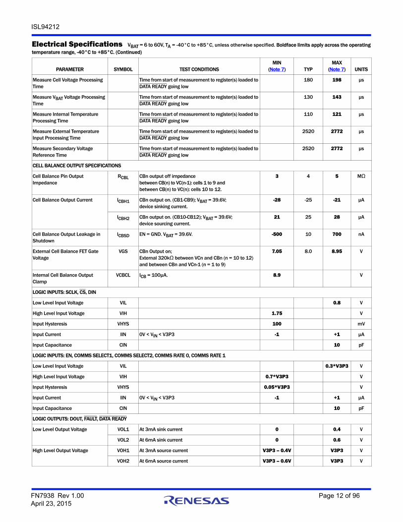
Measure Cell Voltage Processing Time
Time from start of measurement to register(s) loaded to DATA READY going low
180 198 µs
Measure VBAT Voltage Processing Time
Time from start of measurement to register(s) loaded to DATA READY going low
130 143 µs
Measure Internal Temperature Processing Time
Time from start of measurement to register(s) loaded to DATA READY going low
110 121 µs
Measure External Temperature Input Processing Time
Time from start of measurement to register(s) loaded to DATA READY going low
2520 2772 µs
Measure Secondary Voltage Reference Time
Time from start of measurement to register(s) loaded to DATA READY going low
2520 2772 µs
CELL BALANCE OUTPUT SPECIFICATIONS
Cell Balance Pin Output Impedance
RCBL CBn output off impedance between CB(n) to VC(n-1): cells 1 to 9 and between CB(n) to VC(n): cells 10 to 12.
3 4 5 MΩ
Cell Balance Output Current ICBH1 CBn output on. (CB1-CB9); VBAT = 39.6V; device sinking current.
-28 -25 -21 μA
ICBH2 CBn output on. (CB10-CB12); VBAT = 39.6V; device sourcing current.
21 25 28 μA
Cell Balance Output Leakage in Shutdown
ICBSD EN = GND. VBAT = 39.6V. -500 10 700 nA
External Cell Balance FET Gate Voltage
VGS CBn Output on;External 320kΩ between VCn and CBn (n = 10 to 12) and between CBn and VCn-1 (n = 1 to 9)
7.05 8.0 8.95 V
Internal Cell Balance Output Clamp
VCBCL ICB = 100µA. 8.9 V
LOGIC INPUTS: SCLK, CS, DIN
Low Level Input Voltage VIL 0.8 V
High Level Input Voltage VIH 1.75 V
Input Hysteresis VHYS 100 mV
Input Current IIN 0V < VIN < V3P3 -1 +1 µA
Input Capacitance CIN 10 pF
LOGIC INPUTS: EN, COMMS SELECT1, COMMS SELECT2, COMMS RATE 0, COMMS RATE 1
Low Level Input Voltage VIL 0.3*V3P3 V
High Level Input Voltage VIH 0.7*V3P3 V
Input Hysteresis VHYS 0.05*V3P3 V
Input Current IIN 0V < VIN < V3P3 -1 +1 µA
Input Capacitance CIN 10 pF
LOGIC OUTPUTS: DOUT, FAULT, DATA READY
Low Level Output Voltage VOL1 At 3mA sink current 0 0.4 V
VOL2 At 6mA sink current 0 0.6 V
High Level Output Voltage VOH1 At 3mA source current V3P3 – 0.4V V3P3 V
VOH2 At 6mA source current V3P3 – 0.6V V3P3 V
Electrical Specifications VBAT = 6 to 60V, TA = -40°C to +85°C, unless otherwise specified. Boldface limits apply across the operating temperature range, -40°C to +85°C. (Continued)
PARAMETER SYMBOL TEST CONDITIONSMIN
(Note 7) TYPMAX
(Note 7) UNITS
FN7938 Rev 1.00 Page 12 of 96April 23, 2015
ISL94212
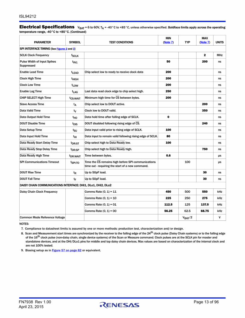
SPI INTERFACE TIMING (See Figures 2 and 3)
SCLK Clock Frequency fSCLK 2 MHz
Pulse Width of Input Spikes Suppressed
tIN1 50 200 ns
Enable Lead Time tLEAD Chip select low to ready to receive clock data 200 ns
Clock High Time tHIGH 200 ns
Clock Low Time tLOW 200 ns
Enable Lag Time tLAG Last data read clock edge to chip select high. 250 ns
CHIP SELECT High Time tCS:WAIT Minimum high time for CS between bytes. 200 ns
Slave Access Time tA Chip select low to DOUT active. 200 ns
Data Valid Time tV Clock low to DOUT valid. 350 ns
Data Output Hold Time tHO Data hold time after falling edge of SCLK. 0 ns
DOUT Disable Time tDIS DOUT disabled following rising edge of CS. 240 ns
Data Setup Time tSU Data input valid prior to rising edge of SCLK. 100 ns
Data Input Hold Time tHI Data input to remain valid following rising edge of SCLK. 80 ns
Data Ready Start Delay Time tDR:ST Chip select high to Data Ready low. 100 ns
Data Ready Stop Delay Time tDR:SP Chip select high to Data Ready high. 750 ns
Data Ready High Time tDR:WAIT Time between bytes. 0.6 µs
SPI Communications Timeout tSPI:TO Time the CS remains high before SPI communications time out - requiring the start of a new command.
100 µs
DOUT Rise Time tR Up to 50pF load. 30 ns
DOUT Fall Time tF Up to 50pF load. 30 ns
DAISY CHAIN COMMUNICATIONS INTERFACE: DHi1, DLo1, DHi2, DLo2
Daisy Chain Clock Frequency Comms Rate (0, 1) = 11 450 500 550 kHz
Comms Rate (0, 1) = 10 225 250 275 kHz
Comms Rate (0, 1) = 01 112.5 125 137.5 kHz
Comms Rate (0, 1) = 00 56.25 62.5 68.75 kHz
Common Mode Reference Voltage VBAT/2 V
NOTES:
7. Compliance to datasheet limits is assured by one or more methods: production test, characterization and/or design.
8. Scan and Measurement start times are synchronized by the receiver to the falling edge of the 24th clock pulse (Daisy Chain systems) or to the falling edge of the 16th clock pulse (non-daisy chain, single device systems) of the Scan or Measure command. Clock pulses are at the SCLK pin for master and standalone devices, and at the DHi/DLo1 pins for middle and top daisy chain devices. Max values are based on characterization of the internal clock and are not 100% tested.
9. Biasing setup as in Figure 57 on page 82 or equivalent.
Electrical Specifications VBAT = 6 to 60V, TA = -40°C to +85°C, unless otherwise specified. Boldface limits apply across the operating temperature range, -40°C to +85°C. (Continued)
PARAMETER SYMBOL TEST CONDITIONSMIN
(Note 7) TYPMAX
(Note 7) UNITS
FN7938 Rev 1.00 Page 13 of 96April 23, 2015
ISL94212
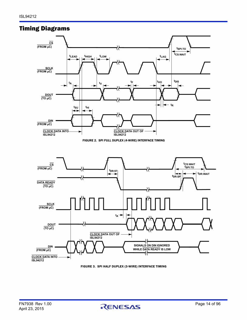
Timing Diagrams
FIGURE 2. SPI FULL DUPLEX (4-WIRE) INTERFACE TIMING
FIGURE 3. SPI HALF DUPLEX (3-WIRE) INTERFACE TIMING
CS
SCLK
DOUT
DIN
tLEAD tHIGH tLOW tLAG
tSPI:TO
tVtAtF tHO tDIS
tRtHItSU
(FROM µC)
(FROM µC)
(FROM µC)
(TO µC)
CLOCK DATA INTOISL94212
CLOCK DATA OUT OFISL94212
tCS:WAIT
CS
SCLK
DOUT
DIN
tDR:WAITtDR:SP
DATA READY
tA
tDR:ST
SIGNALS ON DIN IGNORED
WHILE DATA READY IS LOW
(FROM µC)
(TO µC)
(FROM µC)
(FROM µC)
(TO µC)
CLOCK DATA INTOISL94212
CLOCK DATA OUT OFISL94212
tSPI:TO
tCS:WAIT
FN7938 Rev 1.00 Page 14 of 96April 23, 2015

ISL94212
Typical Performance Curves
FIGURE 4. CELL VOLTAGE READING ERROR FROM 0°C TO +50°C FIGURE 5. CELL VOLTAGE READING ERROR FROM -40°C TO +85°C
FIGURE 6. PACK VOLTAGE READING ERROR FROM 0°C TO +50°C FIGURE 7. PACK VOLTAGE READING ERROR FROM -40°C TO +85°C
FIGURE 8. IC TEMPERATURE ERROR vs PACK VOLTAGE FIGURE 9. VOLTAGE REFERENCE CHECK FUNCTION vs PACK VOLTAGE (AT +25°C)
-40
-30
-20
-10
0
10
20
30
40
0 0.5 1.0 1.5 2.0 2.5 3.0 3.5 4.0 4.5 5.0
RE
AD
ING
ER
RO
R (
mV
)
CELL VOLTAGE (V)
-40
-30
-20
-10
0
10
20
30
40
0 0.5 1.0 1.5 2.0 2.5 3.0 3.5 4.0 4.5 5.0
RE
AD
ING
ER
RO
R (
mV
)
CELL VOLTAGE (V)
RE
AD
ING
ER
RO
R (
mV
)
-500
-400
-300
-200
-100
0
100
200
300
400
500
0 10 20 30 40 50 60PACK VOLTAGE (V)
RE
AD
ING
ER
RO
R (
mV
)
0 10 20 30 40 50 60PACK VOLTAGE (V)
-800
-600
-400
-200
0
200
400
600
800
-5
-4
-3
-2
-1
0
1
2
3
4
0 10 20 30 40 50 60
PACK VOLTAGE (V)
-40°C
-20°C
+25°C
+60°C
+105°C +85°C
NO
RM
AL
IZE
D V
AR
IAT
ION
S (
%)
-0.5
-0.4
-0.3
-0.2
-0.1
0.0
0.1
0.2
0.3
0.4
0.5
6 15 24 33 42 51 60
BG
VR
EF
AC
CU
RA
CY
(m
V)
VBAT (V)
FN7938 Rev 1.00 Page 15 of 96April 23, 2015
ISL94212
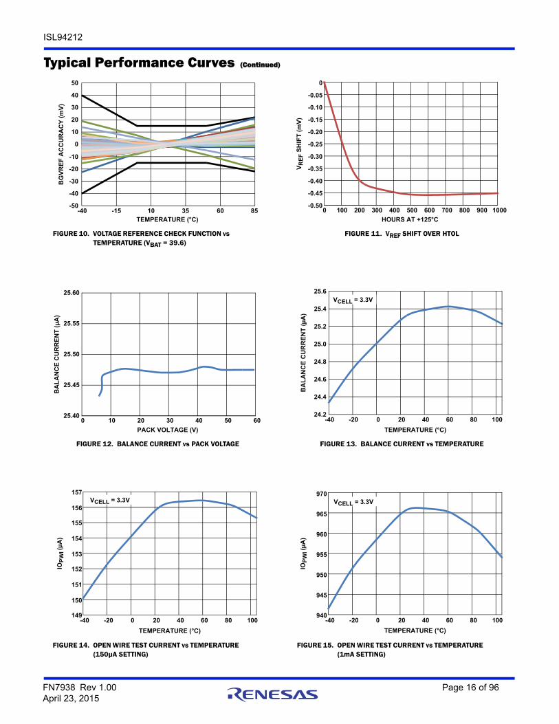
FIGURE 10. VOLTAGE REFERENCE CHECK FUNCTION vs TEMPERATURE (VBAT = 39.6)
FIGURE 11. VREF SHIFT OVER HTOL
FIGURE 12. BALANCE CURRENT vs PACK VOLTAGE FIGURE 13. BALANCE CURRENT vs TEMPERATURE
FIGURE 14. OPEN WIRE TEST CURRENT vs TEMPERATURE (150µA SETTING)
FIGURE 15. OPEN WIRE TEST CURRENT vs TEMPERATURE (1mA SETTING)
Typical Performance Curves (Continued)
-50
-40
-30
-20
-10
0
10
20
30
40
50
-40 -15 10 35 60 85
BG
VR
EF
AC
CU
RA
CY
(m
V)
TEMPERATURE (°C)
-0.50
-0.45
-0.40
-0.35
-0.30
-0.25
-0.20
-0.15
-0.10
-0.05
0
0 100 200 300 400 500 600 700 800 900 1000
HOURS AT +125°C
VR
EF S
HIF
T (
mV
)
25.40
25.45
25.50
25.55
25.60
0 10 20 30 40 50 60
PACK VOLTAGE (V)
BA
LA
NC
E C
UR
RE
NT
(µ
A)
24.2
24.4
24.6
24.8
25.0
25.2
25.4
25.6
-40 -20 0 20 40 60 80 100
TEMPERATURE (°C)
BA
LA
NC
E C
UR
RE
NT
(µ
A)
VCELL = 3.3V
149
150
151
152
153
154
155
156
157
-40 -20 0 20 40 60 80 100
TEMPERATURE (°C)
IOP
WI (
µA
)
VCELL = 3.3V
940
945
950
955
960
965
970
-40 -20 0 20 40 60 80 100
TEMPERATURE (°C)
IOP
WI (
µA
)
VCELL = 3.3V
FN7938 Rev 1.00 Page 16 of 96April 23, 2015
ISL94212
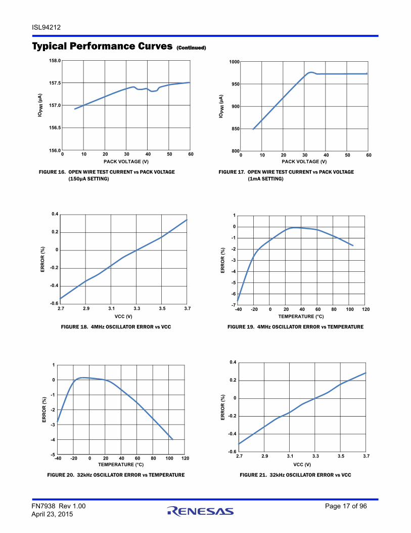
FIGURE 16. OPEN WIRE TEST CURRENT vs PACK VOLTAGE (150µA SETTING)
FIGURE 17. OPEN WIRE TEST CURRENT vs PACK VOLTAGE (1mA SETTING)
FIGURE 18. 4MHz OSCILLATOR ERROR vs VCC FIGURE 19. 4MHz OSCILLATOR ERROR vs TEMPERATURE
FIGURE 20. 32kHz OSCILLATOR ERROR vs TEMPERATURE FIGURE 21. 32kHz OSCILLATOR ERROR vs VCC
Typical Performance Curves (Continued)
156.0
156.5
157.0
157.5
158.0
0 10 20 30 40 50 60
PACK VOLTAGE (V)
IOP
WI (µ
A)
800
850
900
950
1000
0 10 20 30 40 50 60
PACK VOLTAGE (V)
IOP
WI (µ
A)
-0.6
-0.4
-0.2
0
0.2
0.4
2.7 2.9 3.1 3.3 3.5 3.7
VCC (V)
ER
RO
R (
%)
-7
-6
-5
-4
-3
-2
-1
0
1
-40 -20 0 20 40 60 80 100 120
TEMPERATURE (°C)
ER
RO
R (
%)
-5
-4
-3
-2
-1
0
1
-40 -20 0 20 40 60 80 100 120 TEMPERATURE (°C)
ER
RO
R (
%)
-0.6
-0.4
-0.2
0
0.2
0.4
2.7 2.9 3.1 3.3 3.5 3.7
VCC (V)
ER
RO
R (
%)
FN7938 Rev 1.00 Page 17 of 96April 23, 2015
ISL94212
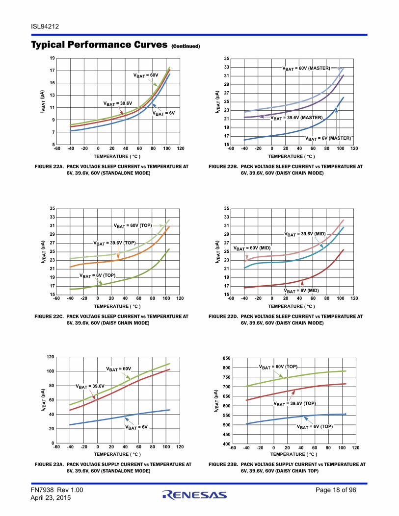
FIGURE 22A. PACK VOLTAGE SLEEP CURRENT vs TEMPERATURE AT 6V, 39.6V, 60V (STANDALONE MODE)
FIGURE 22B. PACK VOLTAGE SLEEP CURRENT vs TEMPERATURE AT 6V, 39.6V, 60V (DAISY CHAIN MODE)
FIGURE 22C. PACK VOLTAGE SLEEP CURRENT vs TEMPERATURE AT 6V, 39.6V, 60V (DAISY CHAIN MODE)
FIGURE 22D. PACK VOLTAGE SLEEP CURRENT vs TEMPERATURE AT 6V, 39.6V, 60V (DAISY CHAIN MODE)
FIGURE 23A. PACK VOLTAGE SUPPLY CURRENT vs TEMPERATURE AT 6V, 39.6V, 60V (STANDALONE MODE)
FIGURE 23B. PACK VOLTAGE SUPPLY CURRENT vs TEMPERATURE AT 6V, 39.6V, 60V (DAISY CHAIN TOP)
Typical Performance Curves (Continued)
5
7
9
11
13
15
17
19
-60 -40 -20 0 20 40 60 80 100 120
TEMPERATURE ( °C )
I VB
AT
(µ
A)
VBAT = 6V
VBAT = 39.6V
VBAT = 60V
15
17
19
21
23
25
27
29
31
33
35
-60 -40 -20 0 20 40 60 80 100 120
TEMPERATURE ( °C )
I VB
AT (
µA
)
VBAT = 6V (MASTER)
VBAT = 39.6V (MASTER)
VBAT = 60V (MASTER)
15
17
19
21
23
25
27
29
31
33
35
-60 -40 -20 0 20 40 60 80 100 120
TEMPERATURE ( °C )
I VB
AT (
µA
)
VBAT = 6V (TOP)
VBAT = 39.6V (TOP)
VBAT = 60V (TOP)
15
17
19
21
23
25
27
29
31
33
35
-60 -40 -20 0 20 40 60 80 100 120
TEMPERATURE ( °C )
I VB
AT (
µA
)
VBAT = 6V (MID)
VBAT = 39.6V (MID)
VBAT = 60V (MID)
0
20
40
60
80
100
120
-60 -40 -20 0 20 40 60 80 100 120
TEMPERATURE ( °C )
I VB
AT (
µA
)
VBAT = 6V
VBAT = 39.6V
VBAT = 60V
400
450
500
550
600
650
700
750
800
850
-60 -40 -20 0 20 40 60 80 100 120
TEMPERATURE ( °C )
I VB
AT (
µA
)
VBAT = 6V (TOP)
VBAT = 39.6V (TOP)
VBAT = 60V (TOP)
FN7938 Rev 1.00 Page 18 of 96April 23, 2015
ISL94212
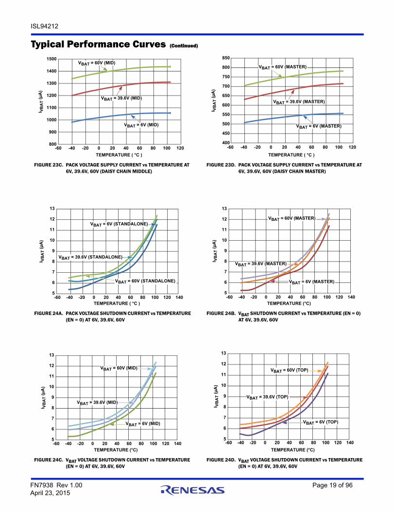
FIGURE 23C. PACK VOLTAGE SUPPLY CURRENT vs TEMPERATURE AT 6V, 39.6V, 60V (DAISY CHAIN MIDDLE)
FIGURE 23D. PACK VOLTAGE SUPPLY CURRENT vs TEMPERATURE AT 6V, 39.6V, 60V (DAISY CHAIN MASTER)
FIGURE 24A. PACK VOLTAGE SHUTDOWN CURRENT vs TEMPERATURE (EN = 0) AT 6V, 39.6V, 60V
FIGURE 24B. VBAT SHUTDOWN CURRENT vs TEMPERATURE (EN = 0) AT 6V, 39.6V, 60V
FIGURE 24C. VBAT VOLTAGE SHUTDOWN CURRENT vs TEMPERATURE (EN = 0) AT 6V, 39.6V, 60V
FIGURE 24D. VBAT VOLTAGE SHUTDOWN CURRENT vs TEMPERATURE (EN = 0) AT 6V, 39.6V, 60V
Typical Performance Curves (Continued)
800
900
1000
1100
1200
1300
1400
1500
-60 -40 -20 0 20 40 60 80 100 120
TEMPERATURE ( °C )
I VB
AT (
µA
)
VBAT = 6V (MID)
VBAT = 39.6V (MID)
VBAT = 60V (MID)
400
450
500
550
600
650
700
750
800
850
-60 -40 -20 0 20 40 60 80 100 120
TEMPERATURE ( °C )
I VB
AT (
µA
)
VBAT = 6V (MASTER)
VBAT = 39.6V (MASTER)
VBAT = 60V (MASTER)
5
6
7
8
9
10
11
12
13
-60 -40 -20 0 20 40 60 80 100 120 140 TEMPERATURE ( °C )
I VB
AT (
µA
)
VBAT = 6V (STANDALONE)
VBAT = 39.6V (STANDALONE)
VBAT = 60V (STANDALONE)
5
6
7
8
9
10
11
12
13
-60 -40 -20 0 20 40 60 80 100 120 140
TEMPERATURE (°C)
I VB
AT (
µA
)VBAT = 60V (MASTER)
VBAT = 6V (MASTER)
VBAT = 39.6V (MASTER)
5
6
7
8
9
10
11
12
13
-60 -40 -20 0 20 40 60 80 100 120 140
TEMPERATURE (°C)
I VB
AT (
µA
)
VBAT = 60V (MID)
VBAT = 6V (MID)
VBAT = 39.6V (MID)
5
6
7
8
9
10
11
12
13
-60 -40 -20 0 20 40 60 80 100 120 140
TEMPERATURE (°C)
I VB
AT (
µA
)
VBAT = 60V (TOP)
VBAT = 39.6V (TOP)
VBAT = 6V (TOP)
FN7938 Rev 1.00 Page 19 of 96April 23, 2015
ISL94212
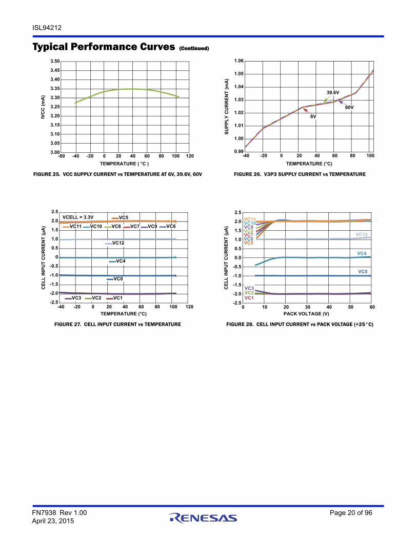
FIGURE 25. VCC SUPPLY CURRENT vs TEMPERATURE AT 6V, 39.6V, 60V FIGURE 26. V3P3 SUPPLY CURRENT vs TEMPERATURE
FIGURE 27. CELL INPUT CURRENT vs TEMPERATURE FIGURE 28. CELL INPUT CURRENT vs PACK VOLTAGE (+25°C)
Typical Performance Curves (Continued)
3.00
3.05
3.10
3.15
3.20
3.25
3.30
3.35
3.40
3.45
3.50
-60 -40 -20 0 20 40 60 80 100 120
TEMPERATURE ( °C )
IVC
C (
mA
)
0.99
1.00
1.01
1.02
1.03
1.04
1.05
1.06
-40 -20 0 20 40 60 80 100
TEMPERATURE (°C)
SU
PP
LY
CU
RR
EN
T (
mA
)
6V
39.6V
60V
-2.5
-2.0
-1.5
-1.0
-0.5
0
0.5
1.0
1.5
2.0
2.5
-40 -20 0 20 40 60 80 100 120
TEMPERATURE (°C)
CE
LL
IN
PU
T C
UR
RE
NT
(µ
A) VC7VC8 VC9VC10VC11 VC6
VC5
VC1VC2VC3
VC12
VC4
VC0
VCELL = 3.3V
-2.5
-2.0
-1.5
-1.0
-0.5
0.0
0.5
1.0
1.5
2.0
2.5
0 10 20 30 40 50 60
PACK VOLTAGE (V)
VC12
VC11VC10VC9VC8VC7VC6VC5
VC4
VC0
CE
LL
IN
PU
T C
UR
RE
NT
(µ
A)
VC3VC2VC1
FN7938 Rev 1.00 Page 20 of 96April 23, 2015

ISL94212
Device Description and OperationThe ISL94212 is a Li-ion battery manager IC that supervises up to 12 series connected cells. Up to 14 ISL94212 devices can be connected in series to support systems with up to 168 cells. The ISL94212 provides accurate monitoring, cell balance control, and diagnostic functions. The ISL94212 includes a voltage reference, 14 bit A/D converter and registers for control and data. An external microcontroller communicates to the ISL94212 through an SPI interface. Series connected ISL94212 devices communicate to each other via a proprietary daisy chain communications interface.
The ISL94212 devices handle daisy chain communications differently depending on their position within the daisy chain. The ISL94212 at one end of the daisy chain acts as a master device for communication purposes. The master device, also called the bottom device, occupies the first position in the daisy chain and communicates to a host microcontroller using an SPI interface. A single daisy chain port then connects the master device to the next device in the daisy chain.
The device at the other end of the daisy chain from the master is the top device. The top device has a single daisy chain port connection to the device below. Devices other than the master and top devices are middle devices. Middle devices have two daisy chain port connections. The up port connects to the device above while the down port connects to the device below. The master ISL94212 device is device number 1. The top device is device number n, where n equals the total number of ISL94212 devices in the daisy chain. The middle devices are numbered 2 to (n-1) with device number 2 being connected to the master device. If n = 2, then there is a master device and a top device, with no middle device.
When multiple ISL94212 devices are connected to a series of cells, their power supply domains are normally non-overlapping. The lower (VSS) supply of each ISL94212 nominally connects to the same potential as the upper (VBAT) supply of the ISL94212 device below.
The ISL94212 provides two multiple parameter measurement “scanning” modes in addition to single parameter direct measurement capability. These scanning modes provide pseudo simultaneous measurement of all cell voltages in the stack. In daisy chain applications all measurement data is sent with the corresponding device stack address (the position within the daisy chain), parameter identifier, and data address. In stand alone applications (non-daisy chain) data is sent without additional address information. This maximizes the throughput for full duplex SPI operation. Daisy chain communication throughput is maximized by allowing streamed data (accessed by a “read all data” address).
The addressed device, the top device and the bottom device act as masters for the purposes of communications timing. All other devices are repeaters, passing data up or down the chain.
The only filtering applied to the ADC measurements is that resulting from external protection circuits and the limited bandwidth of the measurement path. No additional filtering is performed within the part. This arrangement is typically needed
to maintain timing integrity between the cell voltage and pack current measurements. The ISL94212 does not measure current. The system performs this separately using other measurement systems. However, the ISL94212 does apply filtering to the fault detection systems.
Power ModesThe ISL94212 has three main power modes: Normal mode, Sleep mode and Shutdown mode (“off”).
Sleep mode is entered in response to a Sleep command or after a watchdog timeout. Only the communications input circuits, low speed oscillator and internal registers are active in Sleep mode, allowing the part to perform timed scan and balancing activity and to wake up in response to communications.
Drive the enable pin low to place the part in Shutdown mode. When entering Shutdown mode, the internal bias for most of the IC is powered down except digital core, sleep mode regulators, and digital input buffers. When exiting, the device powers up and does not reload the factory programmed configuration data from EEPROM.
The Normal mode consists of an Active state and a Standby state. In the Standby state, all systems are powered and the device is ready and waiting to perform an operation in response to commands from the host microcontroller. In the Active state, the device performs an operation, such as ADC conversion, open wire detection, etc.
Measurement ModesThe ISL94212 provides three types of measurement modes.
• Scan Once
• Scan Continuous
• Measure
In Scan Once mode the part performs the requested scan a single time. In Scan Continuous mode the ISL94212 performs repeated scans at intervals controlled by registers settings. Measure mode allows a single parameter to be measured.
The ISL94212 ignores a Scan or Measure command, when the device is already in a scan mode or measure mode. But, the command passes through to other devices in the daisy chain. All other communications functions respond normally while the device is scanning or measuring.
Measurement Mode CommandsMeasurement modes are activated by commands from an external microcontroller. The ISL94212 uses a memory mapped command structure. Commands are sent to the device using a memory read operation from a specific address. The addresses for the measurement mode commands1 are shown in Table 1.
There are other commands that perform other actions, but these are discussed in other sections.
1. In this document, the terminology for a hex value (e.g., h0000) is modified by a leading value (e.g., 16’) which defines the number of bits. For the measurement mode command address, a value of 6’h02 refers to a binary value of ‘00 0010’.
FN7938 Rev 1.00 Page 21 of 96April 23, 2015

ISL94212
Scan OnceFive different scan functions are available in single scan (Scan Once mode.) Each Scan function is activated by a command from the host microcontroller. The scan functions are:
1. Scan Voltages
2. Scan Temperatures
3. Scan Mixed
4. Scan Wires
5. Scan All
The Scan Once functions are synchronous: all addressed stack devices begin scanning immediately following command receipt. There is a scan start latency between subsequent stack devices of one daisy chain clock cycle (e.g., for a stack of 10 devices with a daisy chain operating at 500kHz, the scan start latency between the bottom and top stack devices is approximately 20µs).
Scan VoltagesThe Scan Voltages command causes the addressed part (or all parts if the common address is used) to scan through the cell voltage inputs followed by the Pack Voltage. IC temperature is also recorded for use with the internal calibration routines. Cell voltages connected to each device are scanned in order from cell-12 (top) to cell-1 (bottom). Cell overvoltage and undervoltage compares are performed on each cell voltage sample. The VBAT and VSS connections are also checked at the end of the scan.
Cell voltage and pack voltage data, along with any fault conditions are stored in local memory ready for reading by the system host microcontroller. If there is a fault condition, the device sets the FAULT pin and returns a fault signal (sent down the stack) on completion of a scan. Devices revert to the standby state on completion of the scan activity.
Scan TemperaturesThe Scan Temperatures command causes the addressed part (or all parts if the common address is used) to scan through the internal and 4 external temperature signals followed by multiplexer loopback and reference measurements. The loopback and reference measurements are part of the internal diagnostics function. Over-temperature compares are performed
on each temperature measurement depending on the condition of the appropriate bit in the Fault Setup register.
Temperature data, along with any fault conditions, are stored in local memory ready for reading by the system host microcontroller. If there is a fault condition, the device sets the FAULT pin and returns a fault signal (sent down the stack) on completion of a scan. Devices revert to the standby state on completion of the scan activity.
Scan MixedThe Scan Mixed command causes the addressed part (or all parts if the common address is used) to scan through the cell voltage inputs (followed by the pack voltage) with a single external input (ExT1) interposed. IC temperature is also recorded for use with the internal calibration routines. Cell voltages connected to each device are scanned in order from cell-12 (top) to cell-1 (bottom). The external input ExT1 is scanned in the middle of the cell voltages such that half the cells are sampled before ExT1 and half after ExT1. This mode allows ExT1 to be used for an external voltage measurement, such as a current sensing and performs it along with the cell voltage measurements, reducing the latency between measurements. Cell overvoltage and cell undervoltage compares are performed on each cell voltage sample. The VBAT and VSS conditions are also checked at the end of the scan.
The Scan Mixed command is intended for use in standalone systems, or by the Master device in stacked applications, and would typically measure a single system parameter, such as battery current. Other stack devices also measure their ExT1 input but these would normally be ignored by the host.
Cell voltage, pack voltage and ExT1 data, along with any fault conditions are stored in local memory ready for reading by the system host microcontroller. Access the data from the ExT1 measurement by a direct Read ET1 Voltage command or by the All Temperatures read command. If there is a fault condition, the device sets the FAULT pin and returns a fault signal (sent down the stack) on completion of a scan. Devices revert to the standby state on completion of the scan activity.
Scan WiresThe Scan Wires command causes the addressed part (or all parts if the common address is used) to measure all the VCn pin voltages while applying load currents to each input pin in turn. This is part of the fault detection system.
If there is a fault condition, the device sets the FAULT pin and returns a fault signal (sent down the stack) on completion of a scan. No cell voltage data is sent as a result of the Scan Wires command. Devices revert to the standby state on completion of this activity.
Scan AllThe Scan All command incorporates the Scan Voltages, Scan Wires and Scan Temperatures commands and causes the addressed part (or all parts if the common address is used) to execute each of these three scan functions once, in sequence (see Figure 29 on page 25 for example on timing).
TABLE 1. MEASUREMENT MODE COMMAND ADDRESSES
REGISTER ADDRESS COMMAND SUFFIX COMMAND
SCAN ONCE
6’h01 6’h00 Scan Voltages
6’h02 6’h00 Scan Temperatures
6’h03 6’h00 Scan Mixed
6’h04 6’h00 Scan Wires
6’h05 6’h00 Scan All
SCAN CONTINUOUS
6’h06 6’h00 Scan Continuous
MEASURE
6’h08 6 bit addr of element to measure Measure
FN7938 Rev 1.00 Page 22 of 96April 23, 2015

ISL94212
Scan ContinuousScan Continuous mode is used primarily for fault monitoring and incorporates the scan voltages, scan temperatures and scan wires commands.
The Scan Continuous command causes the addressed part to set the SCAN bit in the Device Setup register and performs a succession of scans at a predetermined scan rate. Each device operates asynchronously on its own clock. This is similar to the Scan All command except that the scans are repeated at intervals determined by the SCN0-3 bits in the Fault Setup register. The Scan Inhibit command is used to stop scanning (i.e., receipt of this command by the target device resets the SCAN bit and stops the scan continuous function).
The ISL94212 provides an option that pauses cell balancing activity while measuring cell voltages in Scan Continuous mode. This is controlled by the BDDS bit in the Device Setup register. If BDDS is set, then cell balancing is inhibited during cell voltage measurement and for 10ms before the cell voltages are scanned. Balancing is reenabled at the end of the scan to allow balancing to continue. This function only applies during the scan continuous and the auto balance functions and allows the implementation of a circuit arrangement that can be used to diagnose the condition of external balancing components. It is up to the host microcontroller to manually stop balancing functions (if required) when operating a scan once or measure command.
The Scan Continuous scan interval is set using the SCN3:0 bits (lower nibble of the Fault Setup register.) The temperature and wire scans occur at slower rates and depend on the value of the scan interval selected. The scan system is synchronized such that the wire and temperature scans always follow a voltage scan. The three scan sequences, depending on the scans required at a particular instance, are as follows:
• Scan Voltages
• Scan Voltages, Scan Wires
• Scan Voltages, Scan Wires, Scan Temperatures.
The temperature and wire scans occur at 1/5 the voltage scan rate for voltage scan intervals above 128ms. Below this value the temperature scan interval is fixed at 512ms. The behavior of the wire scan interval is determined by the WSCN bit in the Fault Setup register. A bit value of ‘1’ causes the wire scan to be performed at the same rate as the temperature scan. A bit value of ‘0’ causes the wire scan rate to track the voltage scan rate for voltage scan intervals above 512ms while at and below this value the wire scan is performed at a fixed 512ms rate. Table 2 shows the various scan rate combinations available.
Data is not automatically returned while devices are in Scan Continuous mode except in the case where a fault condition is detected. The results of voltage and temperature scans are stored in local volatile memory and may be accessed at any time by the system host microcontroller. Devices may be operated in Scan Continuous mode while in Normal mode or in Sleep mode. Devices revert to the Sleep mode or remain in Normal mode, as applicable on completion of each scan.
The response to a detected fault condition is to send the fault signal, either immediately in the case of standalone devices or daisy chain devices in Normal mode, or following transmission of the wakeup signal if the device is being used in a daisy chain configuration and is in Sleep mode.
To operate the “Scan Continuous” function in Sleep mode the host microcontroller simply configures the ISL94212, starts the Scan Continuous mode and then sends the Sleep command. The ISL94212 then wakes itself up each time a scan is required. Note that for the fastest scan settings (scan interval codes 0000, 0001 and 0010) the main measurement functions do not power down between scans, since the ISL94212 remains in Normal mode.
MeasureThis command allows a single cell voltage, internal temperature, any of the four external temperature inputs or the secondary voltage reference measurements to be made. The command incorporates a 6-bit suffix that contains the address of the required measurement element. See Table 3 on page 24. The device matching the target address responds by conducting the single measurement and loading the result to local memory. The host microcontroller then reads from the target device to obtain the measurement result. All devices revert to the standby state on completion of this activity.
TABLE 2. SCAN CONTINUOUS TIMING MODES
SCANINTERVALSCN3:0
SCANINTERVAL
(ms)
TEMPSCAN(ms)
WIRESCAN
WSCN = 0(ms)
WIRESCAN
WSCN = 1(ms)
0000 16 512 512 512
0001 32 512 512 512
0010 64 512 512 512
0011 128 512 512 512
0100 256 1024 512 1024
0101 512 2048 512 2048
0110 1024 4096 1024 4096
0111 2048 8192 2048 8192
1000 4096 16384 4096 16384
1001 8192 32768 8192 32768
1010 16384 65536 16384 65536
1011 32768 131072 32768 131072
1100 65536 262144 65536 262144
FN7938 Rev 1.00 Page 23 of 96April 23, 2015

ISL94212
Cell Voltage Measurement AccuracyThe cell voltage monitoring system comprises two basic elements; a level shift to eliminate the cell common mode voltage and an analog-to-digital conversion of the cell voltage.
Each ISL94212 is calibrated at a specific cell input voltage value, VNOM. Cell voltage measurement error data is given in “MEASUREMENT SPECIFICATIONS” on page 9 for various voltage and temperature ranges with voltage ranges defined with respect to VNOM. Plots showing the typical error distribution over the full input range are included in the “Typical Performance Curves” section beginning on page 15.
Temperature MonitoringOne internal and four external temperature inputs are provided together with a switched bias voltage output (TEMPREG, pin 29). The voltage at the TEMPREG output is nominally equal to the ADC reference voltage such that the external voltage measurements are ratiometric to the ADC reference (see Figure 61 on page 85).
The temperature inputs are intended for use with external resistor networks using NTC type thermistor sense elements but may also be used as general purpose analog inputs. Each temperature input is applied to the ADC via a multiplexer. The ISL94212 converts the voltage at each input and loads the 14-bit result to the appropriate register.
The TEMPREG output is turned “on” in response to a Scan temperatures or Measure temperature command. A dwell time of 2.5ms is provided to allow external circuits to settle, after which the ADC measures each external input in turn. The TEMPREG output turns “off” after measurements are completed.
Figure 29 on page 25 shows an example temperature scan with the ISL94212 operating in scan continuous mode with a scan interval of 512ms. The preceding voltage and wire scans are shown for comparison.
The external temperature inputs are designed such that an open connection results in the input being pulled up to the full scale input level. This function is provided by a switched 10MΩ pull-up from each input to VCC. This feature is part of the fault detection system and is used to detect open pins.
The internal IC temperature, along with the auxiliary reference voltage and multiplexer loopback signals, are sampled in sequence with the external signals using the scan temperatures command.
The converted value from each temperature input is also compared to the external over-temperature limit and open connection threshold values on condition of the [TST4:1] bits in the Fault Setup register (see “Fault Setup:” on page 64.) If a TSTn bit is set to “1”, then the temperature value is compared to the external temperature threshold and a fault occurs if the measured value is lower than the threshold value. If a TSTn bit is set to “0”, then the temperature measurement is not compared to the threshold value and no fault occurs. The [TST4:1] bits are “0” by default.
TABLE 3. MEASURE COMMAND TARGET ELEMENT ADDRESSES
MEASURECOMMAND
MEASURE ELEMENTADDRESS (SUFFIX) DESCRIPTION
6’h08 6’h00 VBAT Voltage
6’h01 Cell 1 Voltage
6’h02 Cell 2 Voltage
6’h03 Cell 3 Voltage
6’h04 Cell 4 Voltage
6’h05 Cell 5 Voltage
6’h06 Cell 6 Voltage
6’h07 Cell 7 Voltage
6’h08 Cell 8 Voltage
6’h09 Cell 9 Voltage
6’h0A Cell 10 Voltage
6’h0B Cell 11 Voltage
6’h0C Cell 12 Voltage
6’h10 Internal temperature reading
6’h11 External temperature input 1 reading
6’h12 External temperature input 2 reading
6’h13 External temperature input 3 reading
6’h14 External temperature input 4 reading
6’h15 Reference voltage (raw ADC) value. Use to calculate corrected reference value using reference coefficient data. See page 2 data, address 6’h38 – 6’h3A.
FN7938 Rev 1.00 Page 24 of 96April 23, 2015

ISL94212
Cell Balancing FunctionsCell balancing is an important function in a battery pack consisting of a stack of multiple Li-ion cells. As the cells charge and discharge, differences in each cell’s ability to take on and give up charge, typically leads to cells with different states of charge. The problem with a stack of cells having different states of charge is that Li-ion cells have a maximum voltage, above which it should not be charged and a minimum voltage, below which it should not be discharged. The extreme case, where one cell in the stack is at the maximum voltage and one cell is at the minimum voltage, results in a nonfunctional battery stack, since the battery stack cannot be charged or discharged.
Cell balancing is performed using external MOSFETs and external current setting resistors (see Figure 30 on page 30). Each MOSFET is controlled independently by the CB1 to CB12 pins of the ISL94212. The CB1 to CB12 outputs are controlled either directly, or indirectly by an external microcontroller through bits in various control registers.
The balancing functions within the ISL94212 are controlled by multiple registers:
• Balance Setup register (All balance modes, see Table 4)
• Balance Status register (All balance modes, see Table 7 on page 26)
• Device Setup register (auto balance mode only, see Table 13 on page 30)
• Watchdog/Balance Time register (timed and auto balance modes, see Table 9 on page 27)
• Balance Values registers (auto balance only, see example in Table 11 on page 28)
Additional registers are provided for the balance timeout (Timed mode and Auto Balance mode) and balance value (Auto Balance mode only).
Balance Setup Register
The Balance Setup register (see Table 7) contents break down into 4 sub groups.
• Balance wait time: BWT[2:0] bits (also referred to as balance dwell time)
• Balance status pointer: BSP[3:0] bits
• Balance enable: BEN bit
• Balance mode: BMD[1:0] bits
BALANCE WAIT TIMEThe balance wait time control bits, BWT[2:0], set the interval between balancing operations in Auto Balance mode, as shown in Table 5.
Hi-ZHi-ZHi-Z
512ms
2.5V
2.5ms
VOLTAGE SCAN
WIRE SCAN
TEMPERATURE SCAN
2.69ms
TEMPREG PIN
ADC SAMPLING
765µs
59.4ms
FIGURE 29. SCAN TIMING EXAMPLE DURING SCAN CONTINUOUS MODE AND SCAN ALL MODE
TABLE 4. BALANCE SETUP REGISTER (ADDRESS 6’h13)
7 6 5 4 3 2 19
08
BSP2 BSP1 BSP0 BWT2 BWT1 BWT0 BMD1 BMD0
BEN BSP3
TABLE 5. BALANCE WAIT TIME CONTROL BITS
BWT[2:0] SECONDS
000 0
001 1
010 2
011 4
100 8
101 16
110 32
111 64
FN7938 Rev 1.00 Page 25 of 96April 23, 2015

ISL94212
BALANCE STATUS POINTERSee “Balance Status Register”.
BALANCE ENABLEWhen all of the other balance control bits are properly set, setting the balance Enable bit to “1” starts the balance operation. The BEN bit can be set by writing directly to the Balance Setup register or by sending a Balance Enable command.
BALANCE MODEThree methods of cell balance control are provided (see Table 6).
In Manual mode, the host microcontroller directly controls the state of each MOSFET output. In Timed mode, the host microcontroller programs a balance duration value and selects which cells are to be balanced, then starts the balance operation. The ISL94212 turns all the FETs off when the balance duration has been reached. In Auto Balance mode, the host microcontroller programs the ISL94212 to control the balance MOSFETs to remove a programmed “charge delta” value from each cell. The ISL94212 does this by controlling the amount of charge removed from each cell over a number of cycles, rather than trying to balance all cells to a specific voltage.
Balance Status Register
The Balance Status register contents control which external balance FET is turned on during a balance event. Each bit in the Balance Status register controls one external balancing FET, such that Bit 0 [BAL1] controls the cell 1 FET and Bit 11 [BAL12] controls the FET for cell 12 (see Table 7.) Bits are set to enable the balancing for that cell and cleared to disable balancing.
The Balance Status register is a “multiple instance” register. There are 13 locations within this register. The Balance Status Pointer BSP[3:0] points to one of these 13 locations in the register (see Table 7). Only one location in the Balance Status register may be accessed at a time.
The Balance Status register instance at pointer location 0 (BSP[3:0] = 0000) is used for Manual Balance mode and Timed Balance mode. The Balance Status register instances at pointer locations 1 to 12 (BSP[3:0] = 4’h1 to 4’hC) are used for Auto Balance mode. The arrangement is illustrated in Table 7.
In Auto Balance mode, the ISL94212 increments the Balance Status pointer on each auto balance cycle to step through Balance Status register locations 1 to 12. This allows the programming of up to twelve different balance profiles for each Auto Balance operation. On each Auto Balance cycle, the Balance Status pointer increments by one. When the operation encounters a zero value at a pointer location, the Auto Balance operation returns to the pattern at location 1 and resumes balancing with that pattern.
More information about the Auto Balance mode is provided in “Auto Balance Mode” on page 27. Example balancing setup information is provided in “Auto Balance Mode Cell Balancing Example” on page 88.
Manual Balance ModeSelect Manual Balance mode by setting the balance mode bits BMD[1:0] to 2’b01.
To manually control the cells to be balanced, set the balance status pointer to zero: BSP[3:0] = 4’b0000. Then, program the cells to be balanced by setting bits in the Balance Status register (e.g., to balance cell 5, set the BAL5 bit to 1).
Enable balancing, either by setting the BEN bit in the balance setup register or by sending a balance enable command.
Disable balancing either by resetting the BEN bit or by sending a balance inhibit command.
The balance enable and balance inhibit commands may be used with the “Address All” device address to control all devices in a stack simultaneously.
Balancing is not possible in Manual Balance mode while the ISL94212 is in Sleep mode. If the watchdog timer is off and the Sleep command is received while the device is balancing, then balancing stops immediately and the device goes into the Sleep mode.
If the watchdog timer is active during balancing and the device receives the Sleep command, then balancing also stops immediately and the device goes into the Sleep mode, but the WDTM bit is set when the watchdog timer expires. (see Table 8).
TABLE 6. BALANCE MODE CONTROL BITS
BMD[1:0] BALANCE MODE
00 Off
01 Manual
10 Timed
11 Auto
TABLE 7. BALANCE STATUS REGISTER AND BALANCE STATUS POINTER
BSP[3:0]
BALANCE STATUS REGISTER (ADDRESS 6’h14)
BAL12
BAL11
BAL10
BAL9
BAL8
BAL7
BAL 6
BAL5
BAL4
BAL3
BAL2
BAL1
0000 Reserved for Manual and Timed Balance modes
0001 Auto balance status register 1
0010 Auto balance status register 2
0011 Auto balance status register 3
0100 Auto balance status register 4
0101 Auto balance status register 5
0110 Auto balance status register 6
0111 Auto balance status register 7
1000 Auto balance status register 8
1001 Auto balance status register 9
1010 Auto balance status register 10
1011 Auto balance status register 11
1100 Auto balance status register 12
FN7938 Rev 1.00 Page 26 of 96April 23, 2015
ISL94212
The watchdog timer function protects the battery from excess discharge due to balancing, in the event that communications is lost while the part is in Manual Balance mode. All balancing ceases and the device goes into the Sleep mode if the watchdog timeout value is exceeded.
Timed Balance ModeSelect Timed Balance mode by setting the balance mode bits BMD[1:0] to 2’b10.
To set up a timed balance operation, set the balance status pointer to zero: BSP[3:0] = 4’b0000. Then program the cells to be balanced by setting bits in the Balance Status register (e.g., to balance cells 7 and 10, set BAL7 and BAL10 bits to 1).
Set the balance on time. The balance on time is programmable in 20 second intervals from 20 seconds to 42.5 minutes using BTM[6:0] bits. These bits are in locations [13:7] of the Watchdog/Balance Time register. See Tables 9 and 10 for details.
Enable balancing, either by setting the BEN bit in the balance setup register or by sending a balance enable command. The selected balance FETs (corresponding to the bits set in balance status register location 4’b0000) turn on when BEN is asserted and turn off when the balance timeout period is met.
Resetting BEN, either directly or by using the balance inhibit command stops the balancing functions and resets the timer values. When BEN is reasserted, or when a new balance enable command is received, balancing resumes, using the full time specified by the BTM[6:0] bits.
When the balance timeout period is met, the End Of Balance (EOB) bit in the Device Setup register is set and BEN is reset.
Balancing is not possible in the Timed Balance mode while the ISL94212 is in Sleep mode. If the watchdog timer is off and the Sleep command is received while the device is balancing, then balancing stops immediately and the device goes into Sleep mode.
If the watchdog timer is active during balance and the device receives the Sleep command, then balancing also stops immediately and the device enters Sleep mode, but the WDTM bit is set when the watchdog timer expires (see Table 8).
The watchdog can be disabled at any time by writing the watchdog password (6’h3A) to the watchdog password bits [WP5:0] in the Device Setup register (see Table 13 on page 30), and then writing 6’h00 to the watchdog timeout bits [WDG5:0] in the Watchdog/Balance time register (see Table 9).
Auto Balance ModeAuto Balance mode provides the capability to perform balancing autonomously and in an intelligent manner. Thermal issues are accommodated by the provision of the multiple instance Balance Status register and a balance wait time. Cells are balanced with periodic measurements being performed at the balance cycle on time interval (see Table 10). These measurements are used to calculate the reduction in State of Charge (SOC) with each balancing cycle and to terminate balancing of a particular cell when the total SOC change target has been reached.
Select Auto Balance mode by setting the balance mode bits BMD[1:0] to 2’b11.
In Auto Balance mode, the ISL94212 cycles through each balance status register instance and turns on the balancing outputs corresponding to the bits set in each balance status register instance.
AUTO BALANCE SEQUENCEThe Auto Balance sequence is programmed using the “multiple instance” Balance Status register and the balance status pointer bits.
The first cycle of the auto balance operation begins with the balance status pointer at location 1, specifying the first Balance Status register instance. For the next auto balance cycle, the balance status pointer increments to location 2. For each subsequent cycle, the pointer increments to the next Balance Status register instance, until a zero value instance is encountered. At this point the sequence repeats from the
TABLE 8. MANUAL AND TIMED BALANCE MODE WATCHDOG TIMER, BALANCE, SLEEP OPERATION
WATCHDOG TIMER ACTIONS
Off Receiving a Sleep command immediately stops balancing and the device enters the Sleep mode.
On If the device has not received a Sleep command before the watchdog timer expires, then when the watchdog timer does expire, balance stops, the WDTM bit is set and the device enters the Sleep mode.
Receiving a Sleep command immediately stops balancing and the device enters the Sleep mode. Then, when the watchdog timer expires, the WDTM bit is set.
TABLE 9. WATCHDOG/BALANCE TIME REGISTER (ADDRESS 6’h15)
7 6 513
412
311
210
19
08
BTM0 WDG6 WDG5 WDG4 WDG3 WDG2 WDG1 WDG0
BTM6 BTM5 BTM4 BTM3 BTM2 BTM1
TABLE 10. BALANCE CYCLE ON TIME SETTINGS
BTM[6:0] MINUTES
0000000 Disabled
0000001 0.33
0000010 0.67
0000011 1.00
- -
1111101 41.67
1111110 42.00
1111111 42.33
FN7938 Rev 1.00 Page 27 of 96April 23, 2015
ISL94212
balance status register instance at the balance status pointer location 1 until all the cells have met their SOC adjustment value.
For example, to balance odd numbered cells during the first cycle and even numbered cells on the second cycle:(see example in “Cell Balancing – Auto Mode” on page 88.)
• First set the balance status pointer to 1: BSP[3:0] = 0001.
• Specify the even bits by setting Balance Status register bits 0, 2, 4, 6, 8 and 10 to “1”.Balance Status register = 14’h0555
• Set the balance status pointer to 2:BSP[3:0] = 0010.
• Specify the odd bits by setting Balance Status register bits 1, 3, 5, 7, 9 and 11 to “1”.Balance Status register = 14’h0AAA
• Set the balance status pointer to 3: BSP[3:0] = 0011.
• Specify sequence termination by resetting all the bits in the Balance Status register to zero. The next cycle will go back to balance status pointer = 1.Balance Status register = 14’h0000.
• Leave the balance status pointer to 3: BSP[3:0] = 0011.
AUTO BALANCE TIMINGSet the desired interval between balancing cycles using the balance wait time bits BWT[2:0] (locations [4:2] of the Balance Setup register), see Table 4 on page 25 and Table 5 on page 25.
Set the balance cycle on time using the BTM[6:0] bits (locations [13:7] of the Watchdog/Balance Time register), see Tables 9 and 10 on page 27.
Set or clear the BDDS bit, Bit 7 in the Device Setup register, as required. If BDDS is set, then cell balancing is turned off 10ms before the cell voltage scan at the end of each balance cycle. If BDDS is cleared, then balance functions remain “on” during Auto Balance mode cell scan measurements. BDDS must be set in Auto Balance mode when using the standard battery connection configuration shown in Figure 50 on page 73.
AUTO BALANCE (DELTA SOC) VALUEThe next step in setting up an Auto Balance operation is to program the balance value for each cell. The balance value (delta SOC) is the difference between the present charge in a cell and the desired charge for that cell.
The method for calculating the state of charge for a cell is left to the system designer. Typically, determining the state of charge is dependent on the chosen cell type and manufacturer, is dependent on cell voltage, charge and discharge rates, temperature, age of the cell, number of cycles, and other factors. Tables for determining SOC are often available from the battery cell manufacturer.
The balance value itself is a function of the current SOC, required SOC, balancing leg impedance, and sample interval. This value is calculated by the host microcontroller for each cell. The balancing leg impedance is made up of the external balance FET
and balancing resistor. The sample interval is equal to the balance cycle on time period (e.g., each cell voltage is sampled at the end of the balance on time).
The balancing value B for each cell is calculated using the formula shown in Equation 1. (See also “Balance Value Calculation Example” on page 88):
Where:
B = the balance register valueCurrentSOC = the present SOC of the cell (Coulombs)TargetSOC = the required SOC value (Coulombs)Z = the balancing leg impedance (ohms)dt = the sampling time interval
(Balance cycle on time in seconds)8191/5 = a voltage to Hex conversion value
The balancing leg impedance is normally the sum of the balance FET rDS(ON) and the balance resistor.
The balancing value (B) can also be defined as in the set of equations following. Auto balance is guided by Equations 2 and 3:
Where:
dt = Balance cycle on timet = Total balance time
Looking at Equations 2 and 3, the impedance drops out of the equation, leaving only voltage and time elements. Thus, “B” becomes a collection of voltages that integrate during the balance cycle on time, and accumulate over the total balance time period, to equal the programmed delta capacity.
Twelve 28-bit registers are provided for the balance value for each cell. The balance values are programmed for all cells as needed using Balance Value registers 6’h20 to 6’h37 (see Table 11 for the contents of the CELL1 Balance Values Register).
At the end of each balance cycle on time interval the ISL94212 measures the voltage on each of the cells that were balanced during that interval. The measured values are then subtracted from the balance values for those cells. This process continues until the balance value for each cell is zero, at which time the auto balancing process is complete.
TABLE 11. BALANCE VALUES REGISTER CELL1 (ADDRESS 6’h20, 6’h21)
ADDR7
156
145
134
123
112
1019
08
6’20 B0107 B0106 B0105 B0104 B0103 B0102 B0101 B0100
B0113 B0112 B0111 B0110 B0109 B0108
6’21 B0121 B0120 B0119 B0118 B0117 B0116 B0115 B0114
B0127 B0126 B0125 B0124 B0123 B0122
(EQ. 1)B8191
5------------- CurrentSOC T etSOCarg– Z
dt-----=
SOC I t VZ---- t= = (EQ. 2)
B SOCZdt----- V
Z---- t Z
dt----- V
dt----- t= = = (EQ. 3)
FN7938 Rev 1.00 Page 28 of 96April 23, 2015
ISL94212
AUTO BALANCE OPERATIONOnce all of the cell balance FET controls, the balance values and the timers are set up, balance is enabled either by setting the BEN bit in the Balance Setup register or by sending a balance enable command.
Once enabled, the ISL94212 cycles through each instance of the Balance Status register for the duration given by the balance timeout. Between each balance status register instance, the device does a scan all operation and inserts a delay equal to the balance wait time. The process continues with the balance status pointer wrapping back to 1 until all the balance value registers equal zero. If one cell balance value register reaches zero before the others, balancing for that cell stops, but the others continue.
Resetting BEN, either directly or by using the Balance Inhibit command, stops the balancing functions but maintains the current Balance Value register contents. Auto balancing continues from the balance status register location 1 when BEN is reasserted.
When auto balancing is complete, the End of balance (EOB) bit in the Device Setup register is set and BEN bit is reset.
Balancing is not possible using the Auto Balance Mode while the ISL94212 is in Sleep mode. If the sleep command is received while the device is balancing (and the watchdog timer is off) then balancing continues until it is finished and device enters Sleep mode. If the watchdog timer is active during the Auto Balance mode and the device receives the sleep command, then balancing immediately stops and device enters Sleep mode. The WDTM bit is set when the watchdog timer expires (see Table 12).
The watchdog can be disabled at any time by writing the watchdog password (6’h3A) to the watchdog password bits [WP5:0] in the Device Setup register (see Table 13 on page 30) and then writing 6’h00 to the watchdog timeout bits [WDG5:0] in the Watchdog/Balance Time register (see Table 9 on page 27).
Balance FET DriversExternal balancing FETs are controlled by current sources or current sinks attached to the cell balancing (CB) pins. The gate voltage on each FET is then controlled by a locally placed gate-to-source resistor. Voltage clamps are included at each CB output to limit the maximum gate drive voltage. Series gate resistors are used to protect both the external FET and internal IC circuits from external voltage transient effects. An internal gate-to-source connected resistor is used to provide a redundant gate discharge path.
A mix of N-channel and P-channel devices are used for the external FETs in order to remove the need for a charge pump. Cell 12, Cell 11 and Cell 10 balance positions use P-channel devices. The remaining positions use N-channel devices. The basic balance FET drive arrangement is shown in Figure 30.
Additional circuit guidelines are provided in the “Typical Applications Circuits” on page 72.
Reduced cell counts for fewer than 12 cells are accommodated by removing connections to the cells in the middle of the stack first. The top and bottom cell locations are always occupied. See “Operating the ISL94212 with Reduced Cell Counts” on page 78 for suggested cell configurations when using fewer than 12 cells.
TABLE 12. AUTO BALANCE MODE WATCHDOG TIMER, BALANCE, SLEEP OPERATION
WATCHDOG TIMER ACTIONS
Off Receiving a Sleep command puts the device into Sleep mode when the auto balance operation is finished.
On If the device has not received a Sleep command, then when the watchdog timer expires, balance stops, the WDTM bit is set and the device enters Sleep mode.
When the device receives a Sleep command, balance stops immediately. When the watchdog timer expires, the WDTM bit is set and the device enters Sleep mode.
FN7938 Rev 1.00 Page 29 of 96April 23, 2015
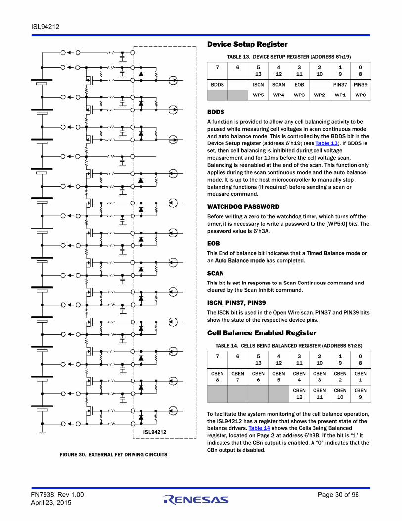
ISL94212
Device Setup Register
BDDSA function is provided to allow any cell balancing activity to be paused while measuring cell voltages in scan continuous mode and auto balance mode. This is controlled by the BDDS bit in the Device Setup register (address 6’h19) (see Table 13). If BDDS is set, then cell balancing is inhibited during cell voltage measurement and for 10ms before the cell voltage scan. Balancing is reenabled at the end of the scan. This function only applies during the scan continuous mode and the auto balance mode. It is up to the host microcontroller to manually stop balancing functions (if required) before sending a scan or measure command.
WATCHDOG PASSWORDBefore writing a zero to the watchdog timer, which turns off the timer, it is necessary to write a password to the [WP5:0] bits. The password value is 6’h3A.
EOBThis End of balance bit indicates that a Timed Balance mode or an Auto Balance mode has completed.
SCANThis bit is set in response to a Scan Continuous command and cleared by the Scan Inhibit command.
ISCN, PIN37, PIN39The ISCN bit is used in the Open Wire scan. PIN37 and PIN39 bits show the state of the respective device pins.
Cell Balance Enabled Register
To facilitate the system monitoring of the cell balance operation, the ISL94212 has a register that shows the present state of the balance drivers. Table 14 shows the Cells Being Balanced register, located on Page 2 at address 6’h3B. If the bit is “1” it indicates that the CBn output is enabled. A “0” indicates that the CBn output is disabled.
FIGURE 30. EXTERNAL FET DRIVING CIRCUITS
ISL78600ISL94212
TABLE 13. DEVICE SETUP REGISTER (ADDRESS 6’h19)
7 6 513
412
311
210
19
08
BDDS ISCN SCAN EOB PIN37 PIN39
WP5 WP4 WP3 WP2 WP1 WP0
TABLE 14. CELLS BEING BALANCED REGISTER (ADDRESS 6’h3B)
7 6 513
412
311
210
19
08
CBEN8
CBEN7
CBEN6
CBEN5
CBEN4
CBEN3
CBEN2
CBEN1
CBEN12
CBEN11
CBEN10
CBEN9
FN7938 Rev 1.00 Page 30 of 96April 23, 2015

ISL94212
System ConfigurationThe ISL94212 provides two communications systems. An SPI synchronous port is provided for communication between a microcontroller and the ISL94212. For standalone (non-daisy chain) systems, the SPI port is the only port needed. In systems where there is more than one ISL94212, daisy chain (asynchronous) ports provide communication between the SPI port on the Master and other ISL94212 devices.
The communications setup is controlled by the COMMS SELECT 1 and COMMS SELECT 2 pins on each device. These pins specify whether the ISL94212 is a standalone device, the daisy chain master, the daisy chain top, or a middle position in the daisy chain. See Figures 31 and 32 and Table 15. This configuration also specifies the use of SPI or daisy chain on the communication ports.
. All communications are conducted through the SPI port in single 8-bit byte increments. The MSB is transmitted first and the LSB is transmitted last.
Commands in non-daisy chain systems are composed of a read/write bit, page address (3 bits), data address (6 bits) and data (6 bits). Commands in daisy chain systems are composed of a device address (4 bits), a read/write bit, page address (3 bits), data address (6 bits), data (6 bits), and CRC (4 bits).
Commands and data are memory mapped to 14-bit data locations. The memory map is arranged in pages. Pages 1 and 2 are used for volatile data. Page 3 contains the action and communications administration commands. Page 4 accesses non-volatile memory. Page 5 is used for factory test.
SPI InterfaceThe ISL94212 operates as a SPI slave capable of bus speeds up to 2Mbps. Four lines make up the SPI interface: SCLK, DIN, DOUT and CS. The SPI interface operates in either full duplex or half duplex mode depending on the daisy chain status of the part.
The DOUT line is normally tri-stated (high impedance) to allow use in a multidrop bus. DOUT is only active when CS is low.
Full Duplex OperationIn non-daisy chain applications, the SPI bus operates as a standard, full duplex, SPI port. Read and write commands are sent to the ISL94212 in 8-bit blocks. CS is taken high between each block. Data flow is controlled by interpreting the first bit of each transaction and counting the requisite number of bytes. It is the host microcontroller’s responsibility to ensure that commands are correctly formulated as an incorrect formulation, (e.g., read bit instead of write bit), would cause the port to lose synchronization. There is a timeout period associated with the CS inactive (high) condition, which resets all the communications counters. This effectively resets the SPI port to a known starting condition. If CS stays high for more than 100µs then the SPI state machine resets.
The ISL94212 responds to read commands by loading the requested data to its output buffer. The output buffer contents are then loaded to the shift register when CS goes low and are shifted out on the DOUT line on the falling edges of SCLK. This sequence continues until all the requested data has been sent. All single register read commands and responses are 2-bytes long. All bytes are handled in pairs during device reads. Device writes are 3-bytes long.
TABLE 15. COMMUNICATIONS MODE CONTROL
COMMSSELECT 1
COMMSSELECT 2
PORT 1COMM
PORT 2COMM
COMMUNICATIONSCONFIGURATION
0 0 SPI(Full Duplex)
Disabled Standalone
0 1 SPI(Half Duplex)
Enabled Daisy Chain, Master device setting
1 0 Daisy Chain Disabled Daisy Chain, Top device setting
1 1 Daisy Chain Enabled Daisy ChainMiddle device setting
SPICOMMS SELECT2
COMMS SELECT1
VSS
FIGURE 31. NON-DAISY CHAIN COMMUNICATIONS CONNECTIONS AND SELECT
ISL94212
SPICOMMS SELECT2
COMMS SELECT1
V3P3
COMMS SELECT2
COMMS SELECT1
V3P3
COMMS SELECT2
COMMS SELECT1
V3P3
VSS
VSS
VSS
Daisy Up
Daisy Down
Daisy Up
FIGURE 32. DAISY CHAIN COMMUNICATIONS CONNECTIONS AND SELECTION
Daisy Down
ISL94212
ISL94212
ISL94212
FN7938 Rev 1.00 Page 31 of 96April 23, 2015
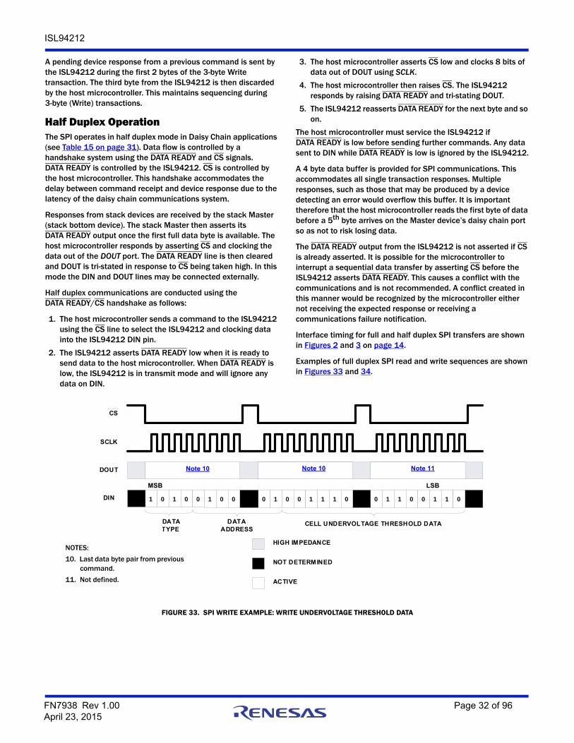
ISL94212
A pending device response from a previous command is sent by the ISL94212 during the first 2 bytes of the 3-byte Write transaction. The third byte from the ISL94212 is then discarded by the host microcontroller. This maintains sequencing during 3-byte (Write) transactions.
Half Duplex OperationThe SPI operates in half duplex mode in Daisy Chain applications (see Table 15 on page 31). Data flow is controlled by a handshake system using the DATA READY and CS signals. DATA READY is controlled by the ISL94212. CS is controlled by the host microcontroller. This handshake accommodates the delay between command receipt and device response due to the latency of the daisy chain communications system.
Responses from stack devices are received by the stack Master (stack bottom device). The stack Master then asserts its DATA READY output once the first full data byte is available. The host microcontroller responds by asserting CS and clocking the data out of the DOUT port. The DATA READY line is then cleared and DOUT is tri-stated in response to CS being taken high. In this mode the DIN and DOUT lines may be connected externally.
Half duplex communications are conducted using the DATA READY/CS handshake as follows:
1. The host microcontroller sends a command to the ISL94212 using the CS line to select the ISL94212 and clocking data into the ISL94212 DIN pin.
2. The ISL94212 asserts DATA READY low when it is ready to send data to the host microcontroller. When DATA READY is low, the ISL94212 is in transmit mode and will ignore any data on DIN.
3. The host microcontroller asserts CS low and clocks 8 bits of data out of DOUT using SCLK.
4. The host microcontroller then raises CS. The ISL94212 responds by raising DATA READY and tri-stating DOUT.
5. The ISL94212 reasserts DATA READY for the next byte and so on.
The host microcontroller must service the ISL94212 if DATA READY is low before sending further commands. Any data sent to DIN while DATA READY is low is ignored by the ISL94212.
A 4 byte data buffer is provided for SPI communications. This accommodates all single transaction responses. Multiple responses, such as those that may be produced by a device detecting an error would overflow this buffer. It is important therefore that the host microcontroller reads the first byte of data before a 5th byte arrives on the Master device’s daisy chain port so as not to risk losing data.
The DATA READY output from the ISL94212 is not asserted if CS is already asserted. It is possible for the microcontroller to interrupt a sequential data transfer by asserting CS before the ISL94212 asserts DATA READY. This causes a conflict with the communications and is not recommended. A conflict created in this manner would be recognized by the microcontroller either not receiving the expected response or receiving a communications failure notification.
Interface timing for full and half duplex SPI transfers are shown in Figures 2 and 3 on page 14.
Examples of full duplex SPI read and write sequences are shown in Figures 33 and 34.
FIGURE 33. SPI WRITE EXAMPLE: WRITE UNDERVOLTAGE THRESHOLD DATA
1 0 1 0 0 1 0 0
DATATYPE
DATA ADDRESS
CELL UNDERVOLTAGE THRESHOLD DATA
0 1 0 0 1 1 1 0 0 1 1 0 0 1 1 0
Note 1 Note 1 Note 2DOUT
DIN
CS
SCLK
HIGH IMPEDANCE
NOT DETERMINED
ACTIVE
NOTES:
10. Last data byte pair from previous command.
11. Not defined.
MSB LSB
Note 10 Note 10 Note 11
FN7938 Rev 1.00 Page 32 of 96April 23, 2015
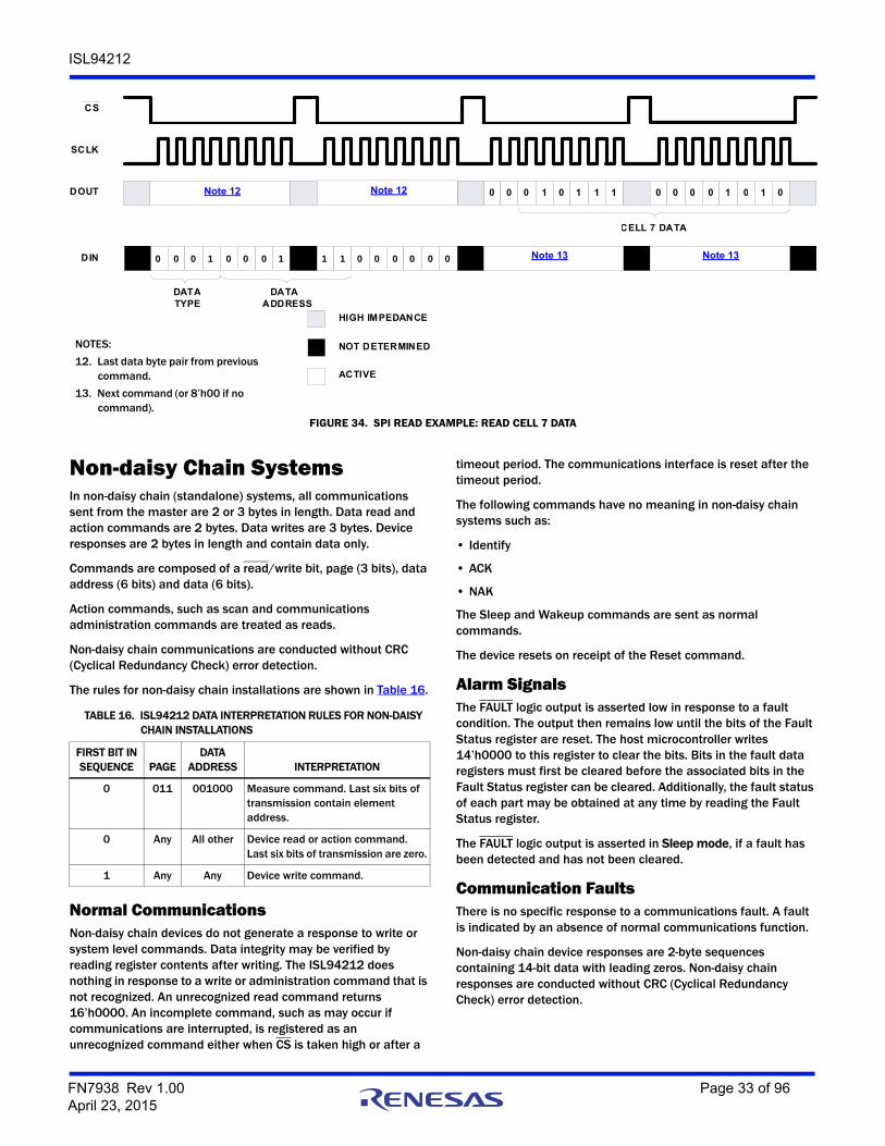
ISL94212
Non-daisy Chain SystemsIn non-daisy chain (standalone) systems, all communications sent from the master are 2 or 3 bytes in length. Data read and action commands are 2 bytes. Data writes are 3 bytes. Device responses are 2 bytes in length and contain data only.
Commands are composed of a read/write bit, page (3 bits), data address (6 bits) and data (6 bits).
Action commands, such as scan and communications administration commands are treated as reads.
Non-daisy chain communications are conducted without CRC (Cyclical Redundancy Check) error detection.
The rules for non-daisy chain installations are shown in Table 16.
Normal CommunicationsNon-daisy chain devices do not generate a response to write or system level commands. Data integrity may be verified by reading register contents after writing. The ISL94212 does nothing in response to a write or administration command that is not recognized. An unrecognized read command returns 16’h0000. An incomplete command, such as may occur if communications are interrupted, is registered as an unrecognized command either when CS is taken high or after a
timeout period. The communications interface is reset after the timeout period.
The following commands have no meaning in non-daisy chain systems such as:
• Identify
• ACK
• NAK
The Sleep and Wakeup commands are sent as normal commands.
The device resets on receipt of the Reset command.
Alarm SignalsThe FAULT logic output is asserted low in response to a fault condition. The output then remains low until the bits of the Fault Status register are reset. The host microcontroller writes 14’h0000 to this register to clear the bits. Bits in the fault data registers must first be cleared before the associated bits in the Fault Status register can be cleared. Additionally, the fault status of each part may be obtained at any time by reading the Fault Status register.
The FAULT logic output is asserted in Sleep mode, if a fault has been detected and has not been cleared.
Communication FaultsThere is no specific response to a communications fault. A fault is indicated by an absence of normal communications function.
Non-daisy chain device responses are 2-byte sequences containing 14-bit data with leading zeros. Non-daisy chain responses are conducted without CRC (Cyclical Redundancy Check) error detection.
FIGURE 34. SPI READ EXAMPLE: READ CELL 7 DATA
HIGH IMPEDANCE
NOT DETERMINED
0 0 0 1 0 0 0 1
DATA TYPE
DATA ADDRESS
CELL 7 DATA
0 0 0 1 0 1 1 1Note 1DOUT
DIN
CS
SCLK
Note 3
ACTIVE
0 0 0 0 1 0 1 0Note 1
1 1 0 0 0 0 0 0 Note 3Note 13 Note 13
NOTES:
12. Last data byte pair from previous command.
13. Next command (or 8’h00 if no command).
Note 12 Note 12
TABLE 16. ISL94212 DATA INTERPRETATION RULES FOR NON-DAISY CHAIN INSTALLATIONS
FIRST BIT INSEQUENCE PAGE
DATAADDRESS INTERPRETATION
0 011 001000 Measure command. Last six bits of transmission contain element address.
0 Any All other Device read or action command. Last six bits of transmission are zero.
1 Any Any Device write command.
FN7938 Rev 1.00 Page 33 of 96April 23, 2015
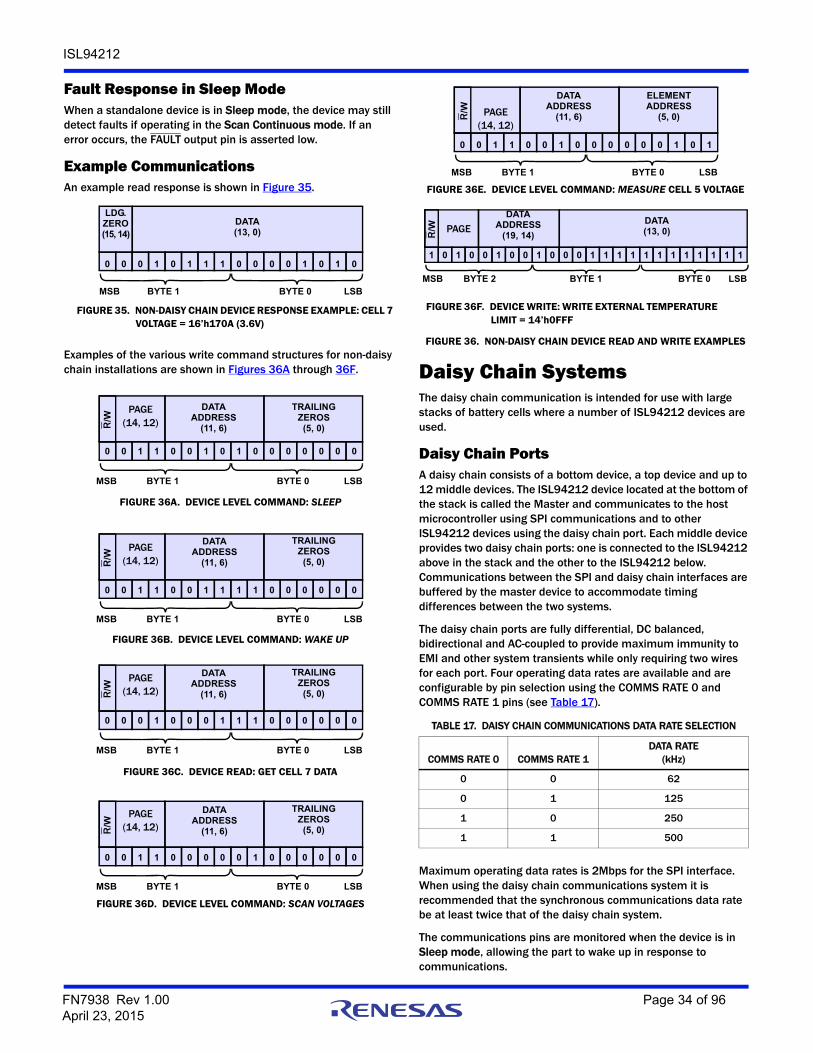
ISL94212
Fault Response in Sleep ModeWhen a standalone device is in Sleep mode, the device may still detect faults if operating in the Scan Continuous mode. If an error occurs, the FAULT output pin is asserted low.
Example CommunicationsAn example read response is shown in Figure 35.
Examples of the various write command structures for non-daisy chain installations are shown in Figures 36A through 36F. Daisy Chain Systems
The daisy chain communication is intended for use with large stacks of battery cells where a number of ISL94212 devices are used.
Daisy Chain PortsA daisy chain consists of a bottom device, a top device and up to 12 middle devices. The ISL94212 device located at the bottom of the stack is called the Master and communicates to the host microcontroller using SPI communications and to other ISL94212 devices using the daisy chain port. Each middle device provides two daisy chain ports: one is connected to the ISL94212 above in the stack and the other to the ISL94212 below. Communications between the SPI and daisy chain interfaces are buffered by the master device to accommodate timing differences between the two systems.
The daisy chain ports are fully differential, DC balanced, bidirectional and AC-coupled to provide maximum immunity to EMI and other system transients while only requiring two wires for each port. Four operating data rates are available and are configurable by pin selection using the COMMS RATE 0 and COMMS RATE 1 pins (see Table 17).
Maximum operating data rates is 2Mbps for the SPI interface. When using the daisy chain communications system it is recommended that the synchronous communications data rate be at least twice that of the daisy chain system.
The communications pins are monitored when the device is in Sleep mode, allowing the part to wake up in response to communications.
FIGURE 36A. DEVICE LEVEL COMMAND: SLEEP
FIGURE 36B. DEVICE LEVEL COMMAND: WAKE UP
FIGURE 36C. DEVICE READ: GET CELL 7 DATA
FIGURE 36D. DEVICE LEVEL COMMAND: SCAN VOLTAGES
FIGURE 35. NON-DAISY CHAIN DEVICE RESPONSE EXAMPLE: CELL 7 VOLTAGE = 16’h170A (3.6V)
0 0 0 1 0 1 1 1 0 0 0 0 1 0 1 0
LDG. ZERO(15, 14)
DATA (13, 0)
BYTE 1 BYTE 0MSB LSB
1 1 0 0 1 0 1 0 0 0 0 0 0 0
PAGE(14, 12)
DATA ADDRESS
(11, 6)
TRAILINGZEROS (5, 0)
BYTE 1 BYTE 0MSB LSB
0 0
R/W
0 0 1 1 0 0 1 1 1 1 0 0 0 0 0 0
DATA ADDRESS
(11, 6)
TRAILINGZEROS (5, 0)
BYTE 1 BYTE 0MSB LSB
PAGE(14, 12)R
/W
0 1 0 0 0 1 1 1 0 0 0 0 0 0
PAGE(14, 12)
DATA ADDRESS
(11, 6)
TRAILINGZEROS (5, 0)
BYTE 1 BYTE 0MSB LSB
0 0
R/W
0 0 1 1 0 0 0 0 0 1 0 0 0 0 0 0
DATA ADDRESS
(11, 6)
TRAILINGZEROS (5, 0)
BYTE 1 BYTE 0MSB LSB
PAGE(14, 12)R
/W
FIGURE 36E. DEVICE LEVEL COMMAND: MEASURE CELL 5 VOLTAGE
FIGURE 36F. DEVICE WRITE: WRITE EXTERNAL TEMPERATURE LIMIT = 14’h0FFF
FIGURE 36. NON-DAISY CHAIN DEVICE READ AND WRITE EXAMPLES
TABLE 17. DAISY CHAIN COMMUNICATIONS DATA RATE SELECTION
COMMS RATE 0 COMMS RATE 1DATA RATE
(kHz)
0 0 62
0 1 125
1 0 250
1 1 500
0 0 1 1 0 0 1 0 0 0 0 0 0 1 0 1
DATA ADDRESS
(11, 6)
ELEMENTADDRESS
(5, 0)
BYTE 1 BYTE 0MSB LSB
PAGE(14, 12)
R/W
1 0 1 0 0 1 0 0 1 0 0 0 1 1 1 1
DATA ADDRESS
(19, 14)
DATA (13, 0)
BYTE 2 BYTE 1MSB
1 1 1 1 1 1 1 1
BYTE 0 LSB
PAGE
R/W
FN7938 Rev 1.00 Page 34 of 96April 23, 2015
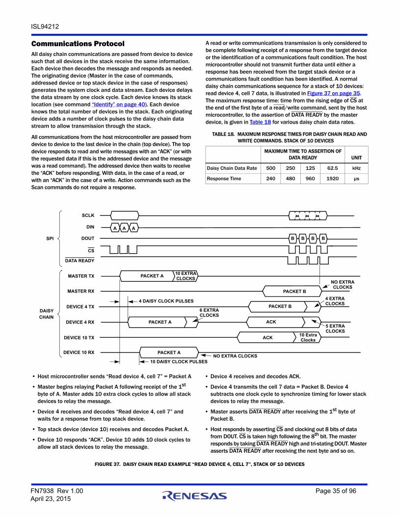
ISL94212
Communications ProtocolAll daisy chain communications are passed from device to device such that all devices in the stack receive the same information. Each device then decodes the message and responds as needed. The originating device (Master in the case of commands, addressed device or top stack device in the case of responses) generates the system clock and data stream. Each device delays the data stream by one clock cycle. Each device knows its stack location (see command “Identify” on page 40). Each device knows the total number of devices in the stack. Each originating device adds a number of clock pulses to the daisy chain data stream to allow transmission through the stack.
All communications from the host microcontroller are passed from device to device to the last device in the chain (top device). The top device responds to read and write messages with an “ACK” (or with the requested data if this is the addressed device and the message was a read command). The addressed device then waits to receive the “ACK” before responding. With data, in the case of a read, or with an “ACK” in the case of a write. Action commands such as the Scan commands do not require a response.
A read or write communications transmission is only considered to be complete following receipt of a response from the target device or the identification of a communications fault condition. The host microcontroller should not transmit further data until either a response has been received from the target stack device or a communications fault condition has been identified. A normal daisy chain communications sequence for a stack of 10 devices: read device 4, cell 7 data, is illustrated in Figure 37 on page 35. The maximum response time: time from the rising edge of CS at the end of the first byte of a read/write command, sent by the host microcontroller, to the assertion of DATA READY by the master device, is given in Table 18 for various daisy chain data rates.
TABLE 18. MAXIMUM RESPONSE TIMES FOR DAISY CHAIN READ AND WRITE COMMANDS. STACK OF 10 DEVICES
MAXIMUM TIME TO ASSERTION OFDATA READY UNIT
Daisy Chain Data Rate 500 250 125 62.5 kHz
Response Time 240 480 960 1920 µs
FIGURE 37. DAISY CHAIN READ EXAMPLE “READ DEVICE 4, CELL 7”, STACK OF 10 DEVICES
• Host microcontroller sends “Read device 4, cell 7” = Packet A
• Master begins relaying Packet A following receipt of the 1st byte of A. Master adds 10 extra clock cycles to allow all stack devices to relay the message.
• Device 4 receives and decodes “Read device 4, cell 7” and waits for a response from top stack device.
• Top stack device (device 10) receives and decodes Packet A.
• Device 10 responds “ACK”. Device 10 adds 10 clock cycles to allow all stack devices to relay the message.
• Device 4 receives and decodes ACK.
• Device 4 transmits the cell 7 data = Packet B. Device 4 subtracts one clock cycle to synchronize timing for lower stack devices to relay the message.
• Master asserts DATA READY after receiving the 1st byte of Packet B.
• Host responds by asserting CS and clocking out 8 bits of data from DOUT. CS is taken high following the 8th bit. The master responds by taking DATA READY high and tri-stating DOUT. Master asserts DATA READY after receiving the next byte and so on.
A A A
B B BB
PACKET A
SCLK
DIN
DOUT
CS
DATA READY
MASTER TX
MASTER RX
DEVICE 4 TX
DEVICE 4 RX
DEVICE 10 TX
DEVICE 10 RX
DAISY
CHAIN
SPI
PACKET A
4 DAISY CLOCK PULSES
PACKET A
10 EXTRACLOCKS
6 EXTRACLOCKS
NO EXTRA CLOCKS10 DAISY CLOCK PULSES
ACK10 ExtraClocks
ACK5 EXTRACLOCKS
PACKET B
4 EXTRACLOCKS
PACKET B
NO EXTRACLOCKS
FN7938 Rev 1.00 Page 35 of 96April 23, 2015
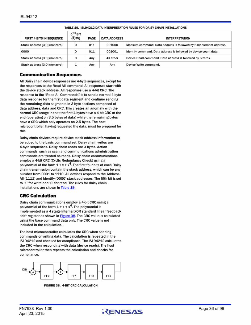
ISL94212
Communication SequencesAll Daisy chain device responses are 4-byte sequences, except for the responses to the Read All command. All responses start with the device stack address. All responses use a 4-bit CRC. The response to the “Read All Commands” is to send a normal 4-byte data response for the first data segment and continue sending the remaining data segments in 3-byte sections composed of data address, data and CRC. This creates an anomaly with the normal CRC usage in that the first 4 bytes have a 4-bit CRC at the end (operating on 3.5 bytes of data) while the remaining bytes have a CRC which only operates on 2.5 bytes. The host microcontroller, having requested the data, must be prepared for this.
Daisy chain devices require device stack address information to be added to the basic command set. Daisy chain writes are 4-byte sequences. Daisy chain reads are 3 bytes. Action commands, such as scan and communications administration commands are treated as reads. Daisy chain communications employ a 4-bit CRC (Cyclic Redundancy Check) using a polynomial of the form 1 + x + x4. The first four bits of each Daisy chain transmission contain the stack address, which can be any number from 0001 to 1110. All devices respond to the Address All (1111) and Identify (0000) stack addresses. The fifth bit is set to ‘1’ for write and ‘0’ for read. The rules for daisy chain installations are shown in Table 19.
CRC CalculationDaisy chain communications employ a 4-bit CRC using a polynomial of the form 1 + x + x4. The polynomial is implemented as a 4 stage internal XOR standard linear feedback shift register as shown in Figure 38. The CRC value is calculated using the base command data only. The CRC value is not included in the calculation.
The host microcontroller calculates the CRC when sending commands or writing data. The calculation is repeated in the ISL94212 and checked for compliance. The ISL94212 calculates the CRC when responding with data (device reads). The host microcontroller then repeats the calculation and checks for compliance.
TABLE 19. ISL94212 DATA INTERPRETATION RULES FOR DAISY CHAIN INSTALLATIONS
FIRST 4 BITS IN SEQUENCE5TH BIT (R/W) PAGE DATA ADDRESS INTERPRETATION
Stack address [3:0] (nonzero) 0 011 001000 Measure command. Data address is followed by 6-bit element address.
0000 0 011 001001 Identify command. Data address is followed by device count data.
Stack address [3:0] (nonzero) 0 Any All other Device Read command. Data address is followed by 6 zeros.
Stack address [3:0] (nonzero) 1 Any Any Device Write command.
+FF0 FF1 FF2 FF3
+DIN
FIGURE 38. 4-BIT CRC CALCULATION
FN7938 Rev 1.00 Page 36 of 96April 23, 2015

ISL94212
Attribute VB_Name = "isl94212evb_crc4_lib"' File - isl94212evb_crc4_lib.bas' Copyright (c) 2010 Intersil' -----------------------------------------------------------------------------Option Explicit'***********************************************************' CRC4 Routines'***********************************************************Public Function CheckCRC4(myArray() As Byte) As Boolean
'returns True if CRC4 checksum (low nibble of last byte in myarray) 'is good. Array can be any length Dim crc4 As Byte
Dim lastnibble As Byte lastnibble = myArray(UBound(myArray)) And &HF
crc4 = CalculateCRC4(myArray) If lastnibble = crc4 Then
CheckCRC4 = True Else
CheckCRC4 = False End If
End Function
Public Sub AddCRC4(myArray() As Byte) 'adds CRC4 checksum (low nibble in last byte in array) 'array can be any length Dim crc4 As Byte
crc4 = CalculateCRC4(myArray)
myArray(UBound(myArray)) = (myArray(UBound(myArray)) And &HF0) Or crc4
End Sub
Public Function CalculateCRC4(ByRef myArray() As Byte) As Byte 'calculates/returns the CRC4 checksum of array contents excluding 'last low nibble. Array can be any length
Dim size As Integer Dim i As Integer Dim j As Integer Dim k As Integer Dim bit0 As Boolean, bit1 As Boolean, bit2 As Boolean, bit3 As
Boolean Dim ff0 As Boolean, ff1 As Boolean, ff2 As Boolean, ff3 As Boolean Dim carry As Boolean Dim arraycopy() As Byte Dim result As Byte
'copy data so we do not clobber source array
ReDim arraycopy(LBound(myArray) To UBound(myArray)) As Byte For i = LBound(myArray) To UBound(myArray)
arraycopy(i) = myArray(i) Next
'initialize bits
bit0 = False bit1 = False bit2 = False bit3 = False 'simple implementation of CRC4 (using polynomial 1 + X + X^4)
For i = LBound(arraycopy) To UBound(arraycopy) 'last nibble is ignored for CRC4 calculations
If i = UBound(arraycopy) Then k = 4
Else k = 8
End If For j = 1 To k
'shift left one bit carry = (arraycopy(i) And &H80) > 0 arraycopy(i) = (arraycopy(i) And &H7F) * 2 'see ISL94212 datasheet, Fig 11: 4-bit CRC calculation
ff0 = carry Xor bit3 ff1 = bit0 Xor bit3 ff2 = bit1 ff3 = bit2 bit0 = ff0 bit1 = ff1
bit2 = ff2 bit3 = ff3
Next jNext i
'combine bits to obtain CRC4 result
result = 0 If bit0 Then
result = result + 1 End If If bit1 Then
result = result + 2 End If If bit2 Then
result = result + 4 End If If bit3 Then
result = result + 8 End If CalculateCRC4 = result
End Function
FIGURE 39. CRC CALCULATION ROUTINE (VISUAL BASIC) EXAMPLE
FN7938 Rev 1.00 Page 37 of 96April 23, 2015
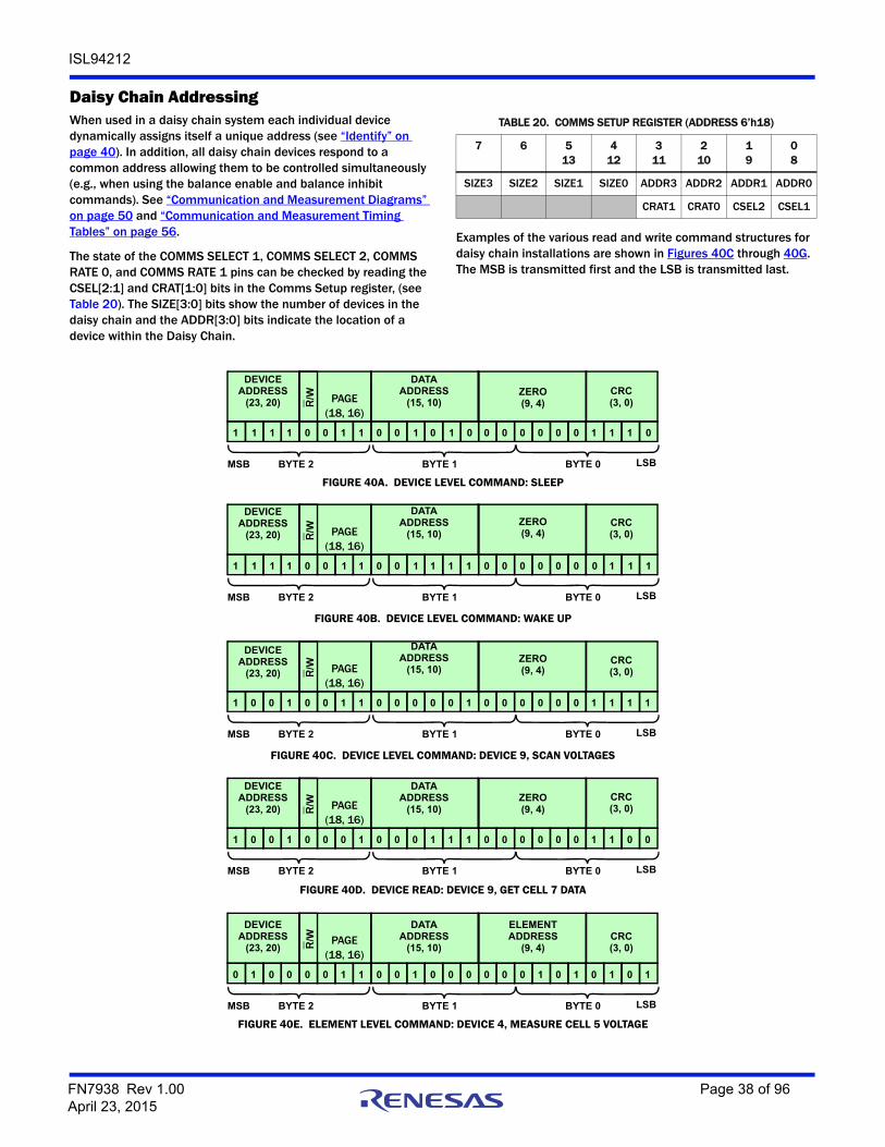
ISL94212
Daisy Chain AddressingWhen used in a daisy chain system each individual device dynamically assigns itself a unique address (see “Identify” on page 40). In addition, all daisy chain devices respond to a common address allowing them to be controlled simultaneously (e.g., when using the balance enable and balance inhibit commands). See “Communication and Measurement Diagrams” on page 50 and “Communication and Measurement Timing Tables” on page 56.
The state of the COMMS SELECT 1, COMMS SELECT 2, COMMS RATE 0, and COMMS RATE 1 pins can be checked by reading the CSEL[2:1] and CRAT[1:0] bits in the Comms Setup register, (see Table 20). The SIZE[3:0] bits show the number of devices in the daisy chain and the ADDR[3:0] bits indicate the location of a device within the Daisy Chain.
Examples of the various read and write command structures for daisy chain installations are shown in Figures 40C through 40G. The MSB is transmitted first and the LSB is transmitted last.
TABLE 20. COMMS SETUP REGISTER (ADDRESS 6’h18)
7 6 513
412
311
210
19
08
SIZE3 SIZE2 SIZE1 SIZE0 ADDR3 ADDR2 ADDR1 ADDR0
CRAT1 CRAT0 CSEL2 CSEL1
FIGURE 40A. DEVICE LEVEL COMMAND: SLEEP
FIGURE 40B. DEVICE LEVEL COMMAND: WAKE UP
FIGURE 40C. DEVICE LEVEL COMMAND: DEVICE 9, SCAN VOLTAGES
FIGURE 40D. DEVICE READ: DEVICE 9, GET CELL 7 DATA
FIGURE 40E. ELEMENT LEVEL COMMAND: DEVICE 4, MEASURE CELL 5 VOLTAGE
0 0 1 1 0 0 1 0 1 0 0 0 0 0 0 0
DATA ADDRESS
(15, 10)ZERO (9, 4)
BYTE 2 BYTE 1MSB LSB
1 1 1 1
DEVICE ADDRESS
(23, 20)
1 1 1 0
CRC (3, 0)
BYTE 0
PAGE(18, 16)
R/W
0 0 1 1 0 0 1 1 1 1 0 0 0 0 0 0
DATA ADDRESS
(15, 10)ZERO (9, 4)
BYTE 2 BYTE 1MSB LSB
1 1 1 1
DEVICE ADDRESS
(23, 20)
0 1 1 1
CRC (3, 0)
BYTE 0
PAGE(18, 16)
R/W
0 0 1 1 0 0 0 0 0 1 0 0 0 0 0 0
DATA ADDRESS
(15, 10)ZERO (9, 4)
BYTE 2 BYTE 1MSB LSB
1 0 0 1
DEVICE ADDRESS
(23, 20)
1 1 1 1
CRC (3, 0)
BYTE 0
PAGE(18, 16)
R/W
0 0 0 1 0 0 0 1 1 1 0 0 0 0 0 0
DATA ADDRESS
(15, 10)ZERO (9, 4)
BYTE 2 BYTE 1MSB LSB
1 0 0 1
DEVICE ADDRESS
(23, 20)
1 1 0 0
CRC (3, 0)
BYTE 0
PAGE(18, 16)
R/W
0 0 1 1 0 0 1 0 0 0 0 0 0 1 0 1
DATA ADDRESS
(15, 10)
ELEMENTADDRESS
(9, 4)
BYTE 2 BYTE 1MSB LSB
0 1 0 0
DEVICE ADDRESS
(23, 20)
0 1 0 1
CRC (3, 0)
BYTE 0
PAGE(18, 16)
R/W
FN7938 Rev 1.00 Page 38 of 96April 23, 2015

ISL94212
Response examples are shown in Figures 41A through 41D.
FIGURE 40F. IDENTIFY COMMAND
FIGURE 40G. DEVICE WRITE: DEVICE 7, WRITE EXTERNAL TEMPERATURE LIMIT = 14’h0FFFFIGURE 40. DAISY CHAIN DEVICE READ AND WRITE EXAMPLES
0 0 1 1 0 0 1 0 0 1 0 0 0 0 0 0
DATA ADDRESS
(15, 10)
DEVICECOUNT
(9, 4)
BYTE 2 BYTE 1MSB LSB
0 0 0 0
DEVICE ADDRESS
(23, 20)
0 1 0 0
CRC (3, 0)
BYTE 0
PAGE(18, 16)
R/W
1 0 1 0 0 1 0 0 1 0 0 0 1 1 1 1
DATA ADDRESS
(23, 18)DATA(17, 4)
BYTE 3 BYTE 2MSB LSB
0 1 1 1
DEVICE ADDRESS
(31, 28)
1 0 0 0
CRC (3, 0)
BYTE 1
1 1 1 1 1 1 1 1
BYTE 0
PAGE(26, 24)
R/W
FIGURE 41A. DEVICE DATA RESPONSE: DEVICE 9, CELL 7 VOLTAGE = 14’h170A (3.6V)
FIGURE 41B. DEVICE COMMUNICATIONS ADMINISTRATION RESPONSE: DEVICE 10, ACK
FIGURE 41C. DEVICE COMMUNICATIONS ADMINISTRATION RESPONSE: IDENTIFY, DEVICE 4, MID STACK DEVICE
0 0 0 1 0 0 0 1 1 1 0 1 0 1 1 1
DATA ADDRESS
(23, 18)DATA(17, 4)
BYTE 3 BYTE 2MSB LSB
1 0 0 1
DEVICE ADDRESS
(31, 28)
0 1 0 0
CRC (3, 0)
BYTE 1
0 0 0 0 1 0 1 0
BYTE 0
PAGE(26, 24)
R/W
0 0 1 1 0 0 1 1 0 0 0 0 0 0 0 0
DATA ADDRESS
(23, 18)ZEROS(17, 4)
BYTE 3 BYTE 2MSB LSB
1 0 1 0
DEVICE ADDRESS
(31, 28)
0 1 0 0
CRC (3, 0)
BYTE 1
0 0 0 0 0 0 0 0
BYTE 0
PAGE(26, 24)
R/W
0 0 1 1 0 0 1 0 0 1 0 0 0 0 0 0
DATA ADDRESS
(23, 18)
DEVICE TYPE/ADDRESS
(17, 4)
BYTE 3 BYTE 2MSB LSB
0 0 0 0
DEVICE ADDRESS
(31, 28)
0 1 1 0
CRC (3, 0)
BYTE 1
0 0 1 1 0 1 0 0
BYTE 0
PAGE(26, 24)R
/W
FN7938 Rev 1.00 Page 39 of 96April 23, 2015
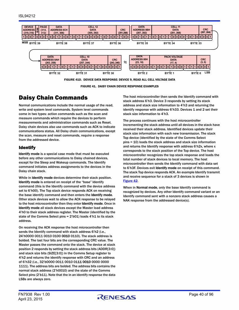
ISL94212
Daisy Chain CommandsNormal communications include the normal usage of the read, write and system level commands. System level commands come in two types: action commands such as the scan and measure commands which require the devices to perform measurements and administration commands such as Reset. Daisy chain devices also use commands such as ACK to indicate communications status. All Daisy chain communications, except the scan, measure and reset commands, require a response from the addressed device.
IdentifyIdentify mode is a special case mode that must be executed before any other communications to Daisy chained devices, except for the Sleep and Wakeup commands. The Identify command initiates address assignments to the devices in the Daisy chain stack.
While in Identify mode devices determine their stack position. Identify mode is entered on receipt of the “base” Identify command (this is the Identify command with the device address set to 6’h00). The Top stack device responds ACK on receiving the base identify command and then enters the Identify mode. Other stack devices wait to allow the ACK response to be relayed to the host microcontroller then they enter Identify mode. Once in Identify mode all stack devices except the Master load address 4’h0 to their stack address register. The Master (identified by the state of the Comms Select pins = 2’b01) loads 4’h1 to its stack address.
On receiving the ACK response the host microcontroller then sends the Identify command with stack address 6’h2 (i.e., 24’h0000 0011 0010 0100 0010 0110). The stack address is bolded. The last four bits are the corresponding CRC value. The Master passes the command onto the stack. The device at stack position 2 responds by setting the stack address bits (ADDR[3:0]) and stack size bits (SIZE[3:0]) in the Comms Setup register to 4’h2 and returns the identify response with CRC and an address of 6’h32 (i.e., 32’b0000 0011 0010 0111 0010 0000 0000 1111). The address bits are bolded. The address bits contains the normal stack address (2’h0010) and the state of the Comms Select pins (2’b11). Note that the in an identify response the data LSBs are always zero.
The host microcontroller then sends the Identify command with stack address 6’h3. Device 3 responds by setting its stack address and stack size information to 4’h3 and returning the identify response with address 6’h33. Devices 1 and 2 set their stack size information to 4’h3.
The process continues with the host microcontroller incrementing the stack address until all devices in the stack have received their stack address. Identified devices update their stack size information with each new transmission. The stack Top device (identified by the state of the Comms Select pins = 10) loads the stack address and stack size information and returns the Identify response with address 6’h2x, where x corresponds to the stack position of the Top device. The host microcontroller recognizes the top stack response and loads the total number of stack devices to local memory. The host microcontroller then sends the Identify command with data set to 6’h3F. Devices exit Identify mode on receipt of this command. The stack Top device responds ACK. An example Identify transmit and receive sequence for a stack of 3 devices is shown in Figure 42.
When in Normal mode, only the base Identify command is recognized by devices. Any other Identify command variant or an Identify command sent with a nonzero stack address causes a NAK response from the addressed device(s).
FIGURE 41D. DEVICE DATA RESPONSE: DEVICE 9, READ ALL CELL VOLTAGE DATA
FIGURE 41. DAISY CHAIN DEVICE RESPONSE EXAMPLES
0 0 0 1 0 0 1 1 0 0 1 0 1 1 1 0
DATA ADDRESS 0CH
(311, 306)
CELL 12DATA
(305, 292)
BYTE 39 BYTE 38MSB
1 0 0 1
DEVICE ADDRESS (319,316)
1 1 0 0
CRC (291,288)
BYTE 37
0 0 0 1 0 1 0 0
BYTE 36
0 0 1 0 1 1 0 1 0 1 1 1
DATA ADDRESS 0BH
(287, 282)
CELL 11DATA
(281, 268)
BYTE 35
0 0 0 1
CRC
(287, 264)
BYTE 34
0 0 0 0 1 0 1 0
BYTE 33
0 0 0 1 1 1 0 1 1 1 1 0
DATA ADDRESS 0AH
(263, 258)
CELL 10DATA
(257, 244)
BYTE 32
0 0 0 1
CRC (243, 240)
BYTE 31
0 0 0 1 0 1 0 0
BYTE 30
0 0 0 0 0 0 0 1 0 0 1 0
DATA ADDRESS 00H
(23, 18)
PACK VOLTAGEDATA(17, 4)
BYTE 2
0 0 0 1
CRC (3, 0)
BYTE 1
1 0 0 0 1 1 1 1
BYTE 0 LSB
PAGE(314, 312)R
/W
FN7938 Rev 1.00 Page 40 of 96April 23, 2015
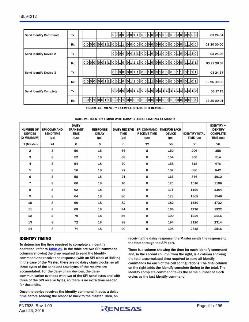
ISL94212
.
IDENTIFY TIMINGTo determine the time required to complete an identify operation, refer to Table 21. In the table are two SPI command columns showing the time required to send the Identify command and receive the response (with an SPI clock of 1MHz.) In the case of the Master, there are no daisy chain clocks, so all three bytes of the send and four bytes of the receive are accumulated. For the daisy chain devices, the daisy communication overlaps with two of the SPI send bytes and with three of the SPI receive bytes, so there is no extra time needed for these bits.
Once the device receives the Identify command, it adds a delay time before sending the response back to the master. Then, on
receiving the daisy response, the Master sends the response to the Host through the SPI port.
There is a column showing the time for each Identify command and, in the second column from the right, is a column showing the total accumulated time required to send all Identify commands for each of the cell configurations. The final column on the right adds the Identify complete timing to the total. The Identify complete command takes the same number of clock cycles as the last Identify command.
FIGURE 42. IDENTIFY EXAMPLE. STACK OF 3 DEVICES
Send Identify Command Tx 03 24 04
Rx 03 30 00 0C
Send Identify Device 2 Tx 03 24 26
Rx 03 27 20 0F
Send Identify Device 3 Tx 03 24 37
Rx 03 26 30 05
Send Identify Complete Tx 03 27 FE
Rx 33 30 00 01
0 0 0 0 0 0 1 1 0 0 1 0 0 1 0 0 0 0 0 0 0 1 0 0
0 0 1 1 0 0 0 0 0 0 0 0 0 0 0 0 0 0 0 0 1 1 0 00 0 0 0 0 0 1 1
0 0 0 0 0 0 1 1 0 0 1 0 0 1 0 0 0 0 1 0 0 1 1 0
0 0 1 0 0 1 1 1 0 0 1 0 0 0 0 0 0 0 0 0 1 1 1 10 0 0 0 0 0 1 1
0 0 0 0 0 0 1 1 0 0 1 0 0 1 0 0 0 0 1 1 0 1 1 1
0 0 1 0 0 1 1 0 0 0 1 1 0 0 0 0 0 0 0 0 0 1 0 10 0 0 0 0 0 1 1
0 0 0 0 0 0 1 1 0 0 1 0 0 1 1 1 1 1 1 1 1 1 1 0
0 0 1 1 0 0 0 0 0 0 0 0 0 0 0 0 0 0 0 0 0 0 0 10 0 1 1 0 0 1 1
TABLE 21. IDENTIFY TIMING WITH DAISY CHAIN OPERATING AT 500kHz
NUMBER OF DEVICES
(2 MINIMUM)
SPI COMMAND SEND TIME
(μs)
DAISY TRANSMIT
TIME (μs)
RESPONSE DELAY
(µs)
DAISY RECEIVE TIME(µs)
SPI COMMAND RECEIVE TIME
(µs)
TIME FOR EACH DEVICE
(µs)IDENTIFY TOTAL
TIME (µs)
IDENTIFY + IDENTIFY
COMPLETE TIME (µs)
1 (Master) 24 0 0 0 32 56 56 56
2 8 50 18 66 8 150 206 356
3 8 52 18 68 8 154 360 514
4 8 54 18 70 8 158 518 676
5 8 56 18 72 8 162 680 842
6 8 58 18 74 8 166 846 1012
7 8 60 18 76 8 170 1016 1186
8 8 62 18 78 8 174 1190 1364
9 8 64 18 80 8 178 1368 1546
10 8 66 18 82 8 182 1550 1732
11 8 68 18 84 8 186 1736 1922
12 8 70 18 86 8 190 1926 2116
13 8 72 18 88 8 194 2120 2314
14 8 74 18 90 8 198 2318 2516
FN7938 Rev 1.00 Page 41 of 96April 23, 2015
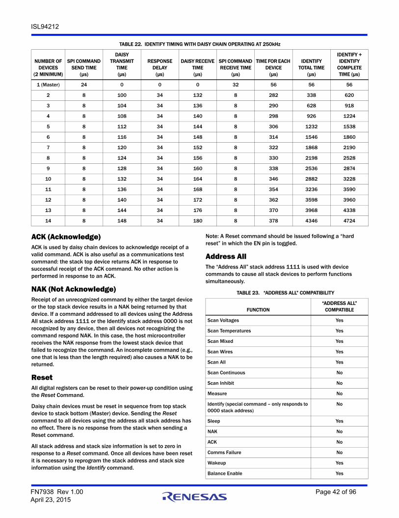
ISL94212
ACK (Acknowledge)ACK is used by daisy chain devices to acknowledge receipt of a valid command. ACK is also useful as a communications test command: the stack top device returns ACK in response to successful receipt of the ACK command. No other action is performed in response to an ACK.
NAK (Not Acknowledge)Receipt of an unrecognized command by either the target device or the top stack device results in a NAK being returned by that device. If a command addressed to all devices using the Address All stack address 1111 or the Identify stack address 0000 is not recognized by any device, then all devices not recognizing the command respond NAK. In this case, the host microcontroller receives the NAK response from the lowest stack device that failed to recognize the command. An incomplete command (e.g., one that is less than the length required) also causes a NAK to be returned.
ResetAll digital registers can be reset to their power-up condition using the Reset Command.
Daisy chain devices must be reset in sequence from top stack device to stack bottom (Master) device. Sending the Reset command to all devices using the address all stack address has no effect. There is no response from the stack when sending a Reset command.
All stack address and stack size information is set to zero in response to a Reset command. Once all devices have been reset it is necessary to reprogram the stack address and stack size information using the Identify command.
Note: A Reset command should be issued following a “hard reset” in which the EN pin is toggled.
Address AllThe “Address All” stack address 1111 is used with device commands to cause all stack devices to perform functions simultaneously.
TABLE 22. IDENTIFY TIMING WITH DAISY CHAIN OPERATING AT 250kHz
NUMBER OF DEVICES
(2 MINIMUM)
SPI COMMAND SEND TIME
(µs)
DAISY TRANSMIT
TIME (μs)
RESPONSE DELAY
(μs)
DAISY RECEIVE TIME(µs)
SPI COMMAND RECEIVE TIME
(µs)
TIME FOR EACH DEVICE
(µs)
IDENTIFY TOTAL TIME
(µs)
IDENTIFY + IDENTIFY
COMPLETE TIME (µs)
1 (Master) 24 0 0 0 32 56 56 56
2 8 100 34 132 8 282 338 620
3 8 104 34 136 8 290 628 918
4 8 108 34 140 8 298 926 1224
5 8 112 34 144 8 306 1232 1538
6 8 116 34 148 8 314 1546 1860
7 8 120 34 152 8 322 1868 2190
8 8 124 34 156 8 330 2198 2528
9 8 128 34 160 8 338 2536 2874
10 8 132 34 164 8 346 2882 3228
11 8 136 34 168 8 354 3236 3590
12 8 140 34 172 8 362 3598 3960
13 8 144 34 176 8 370 3968 4338
14 8 148 34 180 8 378 4346 4724
TABLE 23. “ADDRESS ALL” COMPATIBILITY
FUNCTION“ADDRESS ALL”
COMPATIBLE
Scan Voltages Yes
Scan Temperatures Yes
Scan Mixed Yes
Scan Wires Yes
Scan All Yes
Scan Continuous No
Scan Inhibit No
Measure No
Identify (special command – only responds to 0000 stack address)
No
Sleep Yes
NAK No
ACK No
Comms Failure No
Wakeup Yes
Balance Enable Yes
FN7938 Rev 1.00 Page 42 of 96April 23, 2015

ISL94212
Alarm SignalsBits are set in the following fault data registers:
• Overvoltage register (address 6’h00),
• Undervoltage register (address 6’h01),
• Open Wires register (address 6’h02),
• Over-temperature register (address 6’h06)
Bits are also set in the Fault Status register (address 6’h04) in response to a fault being detected. Additionally, the bits from each of the fault data registers are OR’d and reflected to bits in the Fault Status register (one bit per data register).
A fault is registered when any of the bits in the Fault Status register is asserted. Two fault response methods are provided to indicate the existence of a fault: a fault response is sent via the daisy chain communications interface and the FAULT logic output is asserted low immediately on detection of the fault. The FAULT output remains low until the bits of all fault data registers and the Fault Status register are reset (host microcontroller writes 14’h0000 to these registers to clear the bits).
The Daisy chain fault response is immediate, as long as there is no communication activity on the device ports and comprises the normal fault status register read response. The fault response is only sent for the first fault occurrence. Subsequent faults do not activate the fault response until after the fault status register has been cleared.
If a fault occurs while the device ports are active, then the device waits until communication activity ceases before sending the fault response. The host microcontroller has the option to wait for this response before sending the next message. Alternately, the host microcontroller may send the next message immediately (after allowing the daisy chain ports to clear – see “Sequential Daisy Chain communications” on page 55). Any conflicts resulting from additional transmissions from the stack are recognized by the lack of response from the stack.
Table 24 provides the maximum time from DATA READY going low for the last byte of the normal response to DATA READY going low for the first byte of the fault response in the case where a fault response is held up by active communications.
Further, read communications to the device, return the fault response followed by the requested data. Write communications return only the fault response. Action commands return nothing. The host microcontroller resets the register bits corresponding to the fault by writing 14’h0000 to the Fault Status register, having first cleared the bits in the fault data register(s) if these are set. The device then responds ACK as with a normal write response since the fault status bits are now cleared. This also prevents further fault responses unless the fault reappears, in which case the fault response is repeated.
Watchdog Function
A watchdog function is provided as part of the daisy chain communications fault detection system. The watchdog has no effect in non-daisy chain systems. The watchdog timeout is settable in two ranges using the lower 7 bits of the Watchdog/Balance time register (see Table 25). The low range (7’b0000001 to 7’b0111111) provides timeout settings in 1s increments from 1s to 63s. The high range (7’b1000000 to 7’b1111111) provide timeout settings in 2 minute intervals from 2 minutes to 128 minutes (see Table 26 for details)..
A zero setting (7’b0000000) disables the watchdog function. A watchdog password function is provided to guard against accidental disabling of the watchdog function. The upper 6 bits of the Device Setup register must be set to 6’h3A (111010) to allow the watchdog to be set to zero. The watchdog is disabled by first writing the password to the Device Setup register (see Table 13 on page 30) and then writing zero to the lower bits of the Watchdog/Balance time register. The password function does not prevent changing the watchdog timeout setting to a different nonzero value.
Balance Inhibit Yes
Reset No
Calculate Register Checksum No
Check Register Checksum No
TABLE 24. MAXIMUM TIME BETWEEN DATA READY SIGNALS – DELAYED FAULT RESPONSE
SIGNALSMAXIMUM TIME BETWEEN DATA READY ASSERTIONS UNIT
Daisy Chain Data Rate 500 250 125 62.5 kHz
Fault Response 68 136 272 544 µs
TABLE 23. “ADDRESS ALL” COMPATIBILITY (Continued)
FUNCTION“ADDRESS ALL”
COMPATIBLE
TABLE 25. WATCHDOG/BALANCE TIME REGISTER (ADDRESS 6’h15)
7 6 513
412
311
210
19
08
BTM0 WDG6 WDG5 WDG4 WDG3 WDG2 WDG1 WDG0
BTM6 BTM5 BTM4 BTM3 BTM2 BTM1
TABLE 26. WATCHDOG TIMEOUT SETTINGS
WDG[6:0] TIMEOUT
0000000 Disabled
0000001 1s
0000010 2s
- -
0111110 62s
0111111 63s
1000000 2 min
1000001 4 min
- -
1111110 126 min
1111111 128 min
FN7938 Rev 1.00 Page 43 of 96April 23, 2015
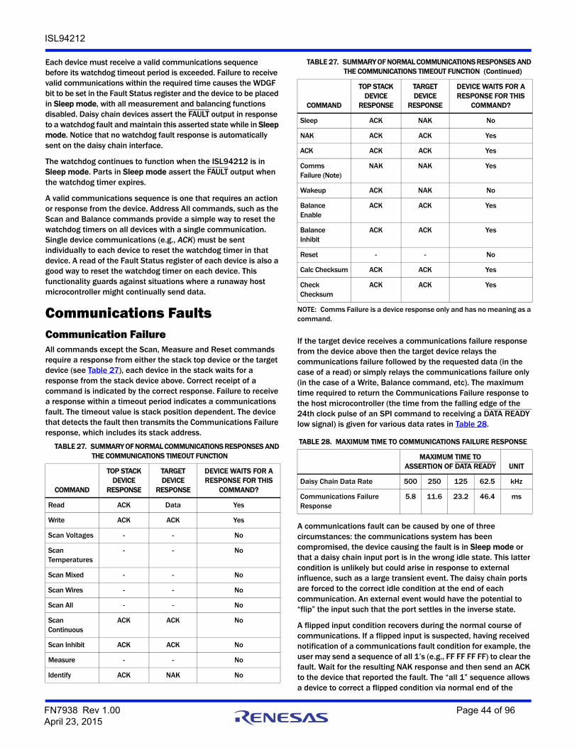
ISL94212
Each device must receive a valid communications sequence before its watchdog timeout period is exceeded. Failure to receive valid communications within the required time causes the WDGF bit to be set in the Fault Status register and the device to be placed in Sleep mode, with all measurement and balancing functions disabled. Daisy chain devices assert the FAULT output in response to a watchdog fault and maintain this asserted state while in Sleep mode. Notice that no watchdog fault response is automatically sent on the daisy chain interface.
The watchdog continues to function when the ISL94212 is in Sleep mode. Parts in Sleep mode assert the FAULT output when the watchdog timer expires.
A valid communications sequence is one that requires an action or response from the device. Address All commands, such as the Scan and Balance commands provide a simple way to reset the watchdog timers on all devices with a single communication. Single device communications (e.g., ACK) must be sent individually to each device to reset the watchdog timer in that device. A read of the Fault Status register of each device is also a good way to reset the watchdog timer on each device. This functionality guards against situations where a runaway host microcontroller might continually send data.
Communications FaultsCommunication FailureAll commands except the Scan, Measure and Reset commands require a response from either the stack top device or the target device (see Table 27), each device in the stack waits for a response from the stack device above. Correct receipt of a command is indicated by the correct response. Failure to receive a response within a timeout period indicates a communications fault. The timeout value is stack position dependent. The device that detects the fault then transmits the Communications Failure response, which includes its stack address.
If the target device receives a communications failure response from the device above then the target device relays the communications failure followed by the requested data (in the case of a read) or simply relays the communications failure only (in the case of a Write, Balance command, etc). The maximum time required to return the Communications Failure response to the host microcontroller (the time from the falling edge of the 24th clock pulse of an SPI command to receiving a DATA READY low signal) is given for various data rates in Table 28.
A communications fault can be caused by one of three circumstances: the communications system has been compromised, the device causing the fault is in Sleep mode or that a daisy chain input port is in the wrong idle state. This latter condition is unlikely but could arise in response to external influence, such as a large transient event. The daisy chain ports are forced to the correct idle condition at the end of each communication. An external event would have the potential to “flip” the input such that the port settles in the inverse state.
A flipped input condition recovers during the normal course of communications. If a flipped input is suspected, having received notification of a communications fault condition for example, the user may send a sequence of all 1’s (e.g., FF FF FF FF) to clear the fault. Wait for the resulting NAK response and then send an ACK to the device that reported the fault. The “all 1” sequence allows a device to correct a flipped condition via normal end of the
TABLE 27. SUMMARY OF NORMAL COMMUNICATIONS RESPONSES AND THE COMMUNICATIONS TIMEOUT FUNCTION
COMMAND
TOP STACKDEVICE
RESPONSE
TARGETDEVICE
RESPONSE
DEVICE WAITS FOR A RESPONSE FOR THIS
COMMAND?
Read ACK Data Yes
Write ACK ACK Yes
Scan Voltages - - No
ScanTemperatures
- - No
Scan Mixed - - No
Scan Wires - - No
Scan All - - No
ScanContinuous
ACK ACK No
Scan Inhibit ACK ACK No
Measure - - No
Identify ACK NAK No
Sleep ACK NAK No
NAK ACK ACK Yes
ACK ACK ACK Yes
CommsFailure (Note)
NAK NAK Yes
Wakeup ACK NAK No
BalanceEnable
ACK ACK Yes
BalanceInhibit
ACK ACK Yes
Reset - - No
Calc Checksum ACK ACK Yes
Check Checksum
ACK ACK Yes
NOTE: Comms Failure is a device response only and has no meaning as a command.
TABLE 28. MAXIMUM TIME TO COMMUNICATIONS FAILURE RESPONSE
MAXIMUM TIME TO ASSERTION OF DATA READY UNIT
Daisy Chain Data Rate 500 250 125 62.5 kHz
Communications Failure Response
5.8 11.6 23.2 46.4 ms
TABLE 27. SUMMARY OF NORMAL COMMUNICATIONS RESPONSES AND THE COMMUNICATIONS TIMEOUT FUNCTION (Continued)
COMMAND
TOP STACKDEVICE
RESPONSE
TARGETDEVICE
RESPONSE
DEVICE WAITS FOR A RESPONSE FOR THIS
COMMAND?
FN7938 Rev 1.00 Page 44 of 96April 23, 2015
ISL94212
communication process. The command FB FF FF FF also works and contains the correct CRC value (should this be a consideration in the way the control software is set up).
If the process mentioned previously results in a Communications Failure response, the next step is for the host microcontroller to send a Sleep command, wait for all stack devices to go to sleep, then send a Wakeup command. If successful then the host microcontroller receives an ACK once all devices are awake. In the case where a single stack device was asleep, the devices above the sleeping device would not have received the Sleep command and would respond to the Wakeup sequence with a NAK due to incomplete communications. The host microcontroller would then send a command (e.g., ACK) to check that all devices are awake. This process can be repeated as often as needed to wakeup sleeping devices.
In the event that the Wakeup command does not generate a response, this is a likely indication that the communications have been compromised. The host microcontroller may send a Sleep command to all units. If the communications watchdog is enabled then all parts go automatically into Sleep mode when the watchdog period expires so long as there are no valid communications activity. Table 27 provides a summary of the normal responses and an indication if the device waits for a response from the various communications commands.
Scan CounterA scan counter is provided to allow confirmation of receipt of the Scan and Measure commands. This is a 4-bit counter located in the Scan Count register (page 1, address 6’h16). The counter increments each time a Scan or Measure command is received. This allows the host microcontroller to compare the counter value before and after the Scan or Measure command was sent to verify receipt. The counter wraps to zero when overflowed.
The scan counter increments whenever the ISL94212 receives a Scan or Measure command. The ISL94212 does not perform a requested scan or measure function if there is already a scan or measure function in progress, but it still increments the scan counter.
Daisy Chain Communications Conflicts Conflicts in the daisy chain system can occur if both a stack device and the host microcontroller are transmitting at the same time, or if more than one stack device transmits at the same time. Conflicts caused by a stack device transmitting at the same time as the host microcontroller are recognized by the absence of the required response (e.g., an ACK response to a write command), or by the scan counter not being incremented in the case of Scan and Measure commands.
Conflicts which arise from more than one device transmitting simultaneously can occur if two devices detect faults at the same time. This can occur when the stack is operating normally (e.g., if two devices register an undervoltage fault in response to a scan voltages command sent to all devices). It is recommended that the host microcontroller checks the Fault Status register contents of all devices whenever a Fault response is received from one device.
Memory ChecksumThere are two checksum operations, one for the EEPROM and one for the Page 2 registers.
Two registers are provided to verify the contents of EEPROM memory. One (Page 4, address 6’h3F) contains the correct checksum value, which is calculated during factory testing at Intersil. The other (Page 5, address 6’h00) contains the checksum value calculated each time the nonvolatile memory is loaded to shadow registers, either after a power cycle or after a device reset. An inequality between these two numbers indicates corruption of the shadow register contents (and possible corruption of EEPROM data). The external microcontroller needs to compare the two registers, since it is not automatic. Resetting the device (using the Reset command) reloads the shadow registers. A persistent difference between these two register values indicates EEPROM corruption.
All Page 2 registers (device configuration registers) are subject to a checksum calculation. A Calculate Register Checksum command calculates the Page 2 checksum and saves the value internally (it is not accessible). The Calculate Register Checksum command may be run any time, but should be sent whenever a Page 2 register is changed.
A Check Register Checksum command recalculates the Page 2 checksum and compares it to the internal value. The occurrence of a Page 2 checksum error sets the PAR bit in the Fault Status register and causes a Fault response accordingly. The normal response to a PAR error is for the host microcontroller to rewrite the Page 2 register contents. A PAR fault also causes the device to cease any scanning or cell balancing activity.
See items 42 through 49 in Table 30 on page 47.
Settling Time Following Diagnostic ActivityThe majority of diagnostic functions within the ISL94212 do not affect other system activity and there is no requirement to wait before conducting further measurements. The exceptions to this are the open wire test and cell balancing functions.
Open Wire TestThe open wire test loads each VCn pin in turn with 150µA or 1mA current. This disturbs the cell voltage measurement while the test is being applied e.g., a 1mA test current applied with an input path resistance of 1kΩ reduces the pin voltage by 1V. The time required for the cell voltage to settle following the open wire test is dependent on the time constant of components used in the cell input circuit. The standard input circuit (Figure 50 on page 73) with the components given in Table 48 on page 77 provide settling to within 0.1mV in approximately 2.8ms. This time should be added at the end of each open wire scan to allow the cell voltages to settle.
Cell BalancingThe standard applications circuit (Figure 50 on page 73) configures the balancing circuits so that the cell input measurement reads close to zero volts when balancing is activated. There are time constants associated with the turn-on
FN7938 Rev 1.00 Page 45 of 96April 23, 2015

ISL94212
and turn-off characteristics of the cell balancing system that must be allowed for when conducting cell voltage measurements.
The turn-on time of the balancing circuit is primarily a function of the 25µA drive current of the cell balancing output and the gate charge characteristic of the MOSFET and needs to be determined for a particular setup. Turn-on settling times to within 2mV of final “on” value are typically less than 5ms.
The turn-off time is a function of the MOSFET gate charge and the VGS connected resistor and capacitor values (for example R27 and C27 in Figure 50 on page 73) and is generally longer than the turn-on time. As with the turn-on case, the turn-off time needs to be determined for the particular components used. Turn-off settling times in the range 10ms to 15ms are typical for settling to within 0.1mV of final value.
Fault Signal FilteringFiltering is provided for the cell overvoltage, cell undervoltage, VBAT open and VSS open tests. These fault signals use a totalizing method in which an unbroken sequence of positive results is required to validate a fault condition. The sequence
length (number of sequential positive samples) is set by the [TOT2:0] bits in the Fault Setup register. See Table 29.
Separate filter functions are provided for each cell input and for the VBAT and VSS open faults. The filter is reset whenever a test results in a negative result (no fault). All filters are reset when the Fault Status register [TOT2:0] bits are changed. When a fault is detected, the [TOT2:0] bits should be rewritten.
The cell overvoltage, cell undervoltage, VBAT open and VSS open faults are sampled at the same time at the end of a Scan Voltages command. The cell undervoltage and cell overvoltage signals are also checked following a Measure cell voltage command.
Fault DiagnosticsThe ISL94212 incorporates extensive fault diagnostics functions, which include cell overvoltage and undervoltage as well as open cell input detection. The current status of all faults is accessible using the ISL94212 registers. Table 30 shows a summary of commands and responses for the various fault diagnostics functions.
TABLE 29. FAULT TOTALIZING TIME (ms) AS A FUNCTION OF SCAN INTERVAL AND NUMBER OF TOTALIZED SAMPLES
SCANINTERVAL
CODE
SCANINTERVAL
(ms)
TOTALIZE – FAULT SETUP REGISTER
1000
2001
4010
8011
16100
32101
64110
128111
0000 16 16 32 64 128 256 512 1024 2048
0001 32 32 64 128 256 512 1024 2048 4096
0010 64 64 128 256 512 1024 2048 4096 8192
0011 128 128 256 512 1024 2048 4096 8192 16384
0100 256 256 512 1024 2048 4096 8192 16384 32768
0101 512 512 1024 2048 4096 8192 16384 32768 65536
0110 1024 1024 2048 4096 8192 16384 32768 65536 131072
0111 2048 2048 4096 8192 16384 32768 65536 131072 262144
1000 4096 4096 8192 16384 32768 65536 131072 262144 524288
1001 8192 8192 16384 32768 65536 131072 262144 524288 1048576
1010 16384 16384 32768 65536 131072 262144 524288 1048576 2097152
1011 32768 32768 65536 131072 262144 524288 1048576 2097152 4194304
1100 65536 65536 131072 262144 524288 1048576 2097152 4194304 8388608
FN7938 Rev 1.00 Page 46 of 96April 23, 2015
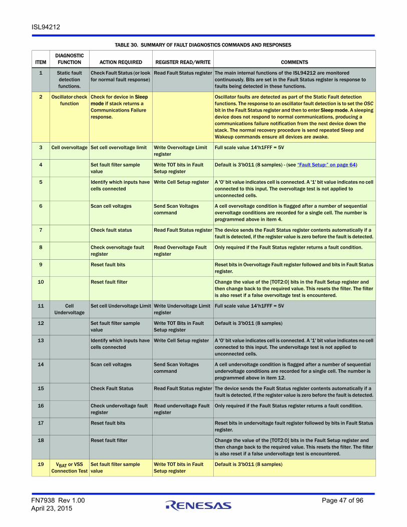
ISL94212
TABLE 30. SUMMARY OF FAULT DIAGNOSTICS COMMANDS AND RESPONSES
ITEMDIAGNOSTIC FUNCTION ACTION REQUIRED REGISTER READ/WRITE COMMENTS
1 Static fault detection functions.
Check Fault Status (or look for normal fault response)
Read Fault Status register The main internal functions of the ISL94212 are monitored continuously. Bits are set in the Fault Status register is response to faults being detected in these functions.
2 Oscillator check function
Check for device in Sleep mode if stack returns a Communications Failure response.
Oscillator faults are detected as part of the Static Fault detection functions. The response to an oscillator fault detection is to set the OSC bit in the Fault Status register and then to enter Sleep mode. A sleeping device does not respond to normal communications, producing a communications failure notification from the next device down the stack. The normal recovery procedure is send repeated Sleep and Wakeup commands ensure all devices are awake.
3 Cell overvoltage Set cell overvoltage limit Write Overvoltage Limit register
Full scale value 14'h1FFF = 5V
4 Set fault filter sample value
Write TOT bits in Fault Setup register
Default is 3'b011 (8 samples) - (see “Fault Setup:” on page 64)
5 Identify which inputs have cells connected
Write Cell Setup register A '0' bit value indicates cell is connected. A '1' bit value indicates no cell connected to this input. The overvoltage test is not applied to unconnected cells.
6 Scan cell voltages Send Scan Voltages command
A cell overvoltage condition is flagged after a number of sequential overvoltage conditions are recorded for a single cell. The number is programmed above in item 4.
7 Check fault status Read Fault Status register The device sends the Fault Status register contents automatically if a fault is detected, if the register value is zero before the fault is detected.
8 Check overvoltage fault register
Read Overvoltage Fault register
Only required if the Fault Status register returns a fault condition.
9 Reset fault bits Reset bits in Overvoltage Fault register followed and bits in Fault Status register.
10 Reset fault filter Change the value of the [TOT2:0] bits in the Fault Setup register and then change back to the required value. This resets the filter. The filter is also reset if a false overvoltage test is encountered.
11 Cell Undervoltage
Set cell Undervoltage Limit Write Undervoltage Limit register
Full scale value 14'h1FFF = 5V
12 Set fault filter sample value
Write TOT Bits in Fault Setup register
Default is 3'b011 (8 samples)
13 Identify which inputs have cells connected
Write Cell Setup register A '0' bit value indicates cell is connected. A '1' bit value indicates no cell connected to this input. The undervoltage test is not applied to unconnected cells.
14 Scan cell voltages Send Scan Voltages command
A cell undervoltage condition is flagged after a number of sequential undervoltage conditions are recorded for a single cell. The number is programmed above in item 12.
15 Check Fault Status Read Fault Status register The device sends the Fault Status register contents automatically if a fault is detected, if the register value is zero before the fault is detected.
16 Check undervoltage fault register
Read undervoltage Fault register
Only required if the Fault Status register returns a fault condition.
17 Reset fault bits Reset bits in undervoltage fault register followed by bits in Fault Status register.
18 Reset fault filter Change the value of the [TOT2:0] bits in the Fault Setup register and then change back to the required value. This resets the filter. The filter is also reset if a false undervoltage test is encountered.
19 VBAT or VSS Connection Test
Set fault filter sample value
Write TOT bits in Fault Setup register
Default is 3'b011 (8 samples)
FN7938 Rev 1.00 Page 47 of 96April 23, 2015
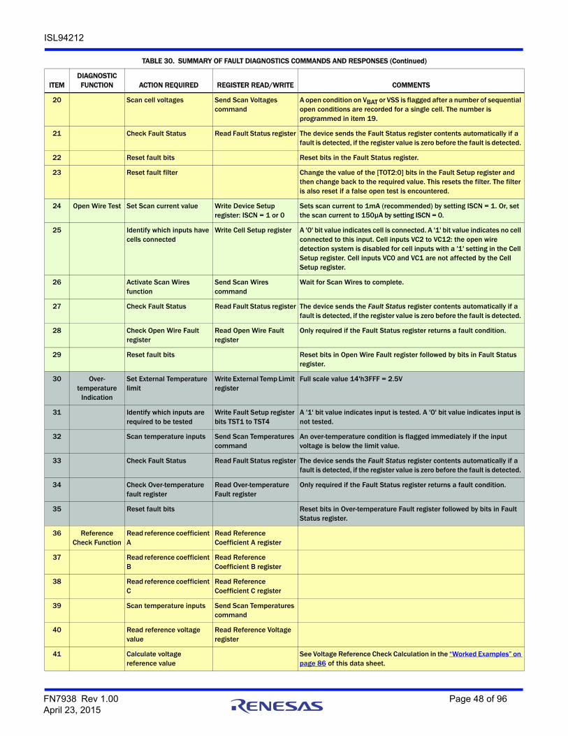
ISL94212
20 Scan cell voltages Send Scan Voltages command
A open condition on VBAT or VSS is flagged after a number of sequential open conditions are recorded for a single cell. The number is programmed in item 19.
21 Check Fault Status Read Fault Status register The device sends the Fault Status register contents automatically if a fault is detected, if the register value is zero before the fault is detected.
22 Reset fault bits Reset bits in the Fault Status register.
23 Reset fault filter Change the value of the [TOT2:0] bits in the Fault Setup register and then change back to the required value. This resets the filter. The filter is also reset if a false open test is encountered.
24 Open Wire Test Set Scan current value Write Device Setup register: ISCN = 1 or 0
Sets scan current to 1mA (recommended) by setting ISCN = 1. Or, set the scan current to 150µA by setting ISCN = 0.
25 Identify which inputs have cells connected
Write Cell Setup register A '0' bit value indicates cell is connected. A '1' bit value indicates no cell connected to this input. Cell inputs VC2 to VC12: the open wire detection system is disabled for cell inputs with a '1' setting in the Cell Setup register. Cell inputs VC0 and VC1 are not affected by the Cell Setup register.
26 Activate Scan Wires function
Send Scan Wires command
Wait for Scan Wires to complete.
27 Check Fault Status Read Fault Status register The device sends the Fault Status register contents automatically if a fault is detected, if the register value is zero before the fault is detected.
28 Check Open Wire Fault register
Read Open Wire Fault register
Only required if the Fault Status register returns a fault condition.
29 Reset fault bits Reset bits in Open Wire Fault register followed by bits in Fault Status register.
30 Over-temperature
Indication
Set External Temperature limit
Write External Temp Limit register
Full scale value 14'h3FFF = 2.5V
31 Identify which inputs are required to be tested
Write Fault Setup register bits TST1 to TST4
A '1' bit value indicates input is tested. A '0' bit value indicates input is not tested.
32 Scan temperature inputs Send Scan Temperatures command
An over-temperature condition is flagged immediately if the input voltage is below the limit value.
33 Check Fault Status Read Fault Status register The device sends the Fault Status register contents automatically if a fault is detected, if the register value is zero before the fault is detected.
34 Check Over-temperature fault register
Read Over-temperature Fault register
Only required if the Fault Status register returns a fault condition.
35 Reset fault bits Reset bits in Over-temperature Fault register followed by bits in Fault Status register.
36 Reference Check Function
Read reference coefficient A
Read Reference Coefficient A register
37 Read reference coefficient B
Read Reference Coefficient B register
38 Read reference coefficient C
Read Reference Coefficient C register
39 Scan temperature inputs Send Scan Temperatures command
40 Read reference voltage value
Read Reference Voltage register
41 Calculate voltage reference value
See Voltage Reference Check Calculation in the “Worked Examples” on page 86 of this data sheet.
TABLE 30. SUMMARY OF FAULT DIAGNOSTICS COMMANDS AND RESPONSES (Continued)
ITEMDIAGNOSTIC FUNCTION ACTION REQUIRED REGISTER READ/WRITE COMMENTS
FN7938 Rev 1.00 Page 48 of 96April 23, 2015
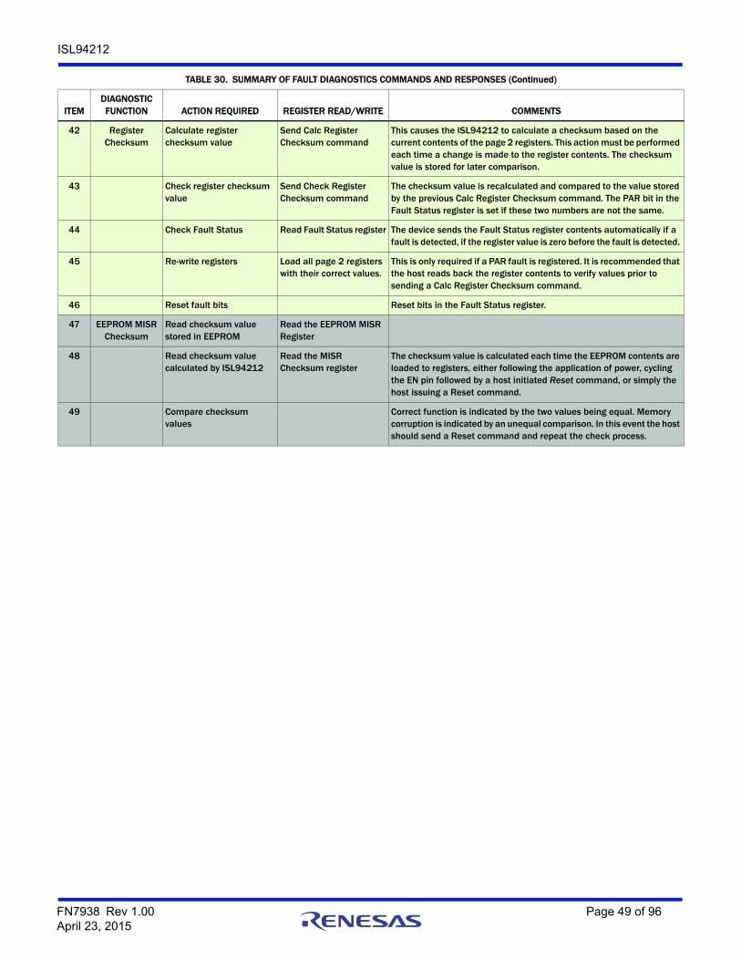
ISL94212
42 Register Checksum
Calculate register checksum value
Send Calc Register Checksum command
This causes the ISL94212 to calculate a checksum based on the current contents of the page 2 registers. This action must be performed each time a change is made to the register contents. The checksum value is stored for later comparison.
43 Check register checksum value
Send Check Register Checksum command
The checksum value is recalculated and compared to the value stored by the previous Calc Register Checksum command. The PAR bit in the Fault Status register is set if these two numbers are not the same.
44 Check Fault Status Read Fault Status register The device sends the Fault Status register contents automatically if a fault is detected, if the register value is zero before the fault is detected.
45 Re-write registers Load all page 2 registers with their correct values.
This is only required if a PAR fault is registered. It is recommended that the host reads back the register contents to verify values prior to sending a Calc Register Checksum command.
46 Reset fault bits Reset bits in the Fault Status register.
47 EEPROM MISR Checksum
Read checksum value stored in EEPROM
Read the EEPROM MISR Register
48 Read checksum value calculated by ISL94212
Read the MISR Checksum register
The checksum value is calculated each time the EEPROM contents are loaded to registers, either following the application of power, cycling the EN pin followed by a host initiated Reset command, or simply the host issuing a Reset command.
49 Compare checksum values
Correct function is indicated by the two values being equal. Memory corruption is indicated by an unequal comparison. In this event the host should send a Reset command and repeat the check process.
TABLE 30. SUMMARY OF FAULT DIAGNOSTICS COMMANDS AND RESPONSES (Continued)
ITEMDIAGNOSTIC FUNCTION ACTION REQUIRED REGISTER READ/WRITE COMMENTS
FN7938 Rev 1.00 Page 49 of 96April 23, 2015

ISL94212
Sleep ModeDevices enter Sleep mode in response to a Sleep command, a watchdog time out or in response to an oscillator fault. Devices wakeup in response to a Wakeup command or to a Scan Continuous cycle if the device was set to Sleep mode with Scan Continuous mode active.
Using a Sleep command or Wakeup command does not require that the devices in a stack are identified first. They do not need to know their position in the stack.
In a daisy chain system, the Sleep command must be written using the Address All stack address: 1111. The command is not recognized if sent with an individual device address and causes the addressed device to respond NAK. The top stack device responds ACK on receiving a valid Sleep command.
Having received a valid Sleep command, devices wait before entering the Sleep mode. This is to allow time for the top stack device to respond ACK, or for all devices that don’t recognize the command to respond NAK, and for the host microcontroller to respond with another command. Receipt of any valid communications on port 1 of the ISL94212 before the wait period expires cancels the Sleep command. Receipt of another Sleep command restarts the wait timers. Table 31 provides the maximum wait time for various daisy chain data rates. The communications fault checking timeout is not applied to the Sleep command. A problem with the communications is indicated by a lack of response to the host microcontroller. The host microcontroller may choose to do nothing if no response is received in which case devices that received the Sleep command go to sleep when the wait time expires. Devices that do not receive the message go to sleep when their watchdog timer expires (as long as this is enabled).
WakeupThe host microcontroller wakes up a stack of sleeping devices by sending the Wakeup command to the Master stack device. The Wakeup command must be written using the Address All stack address: 1111. The command is not recognized if sent with an individual device address and causes the Master device to respond NAK.
The Master exits Sleep mode on receipt of a valid Wakeup command and proceeds to transmit the Wakeup signal to the next device in the stack. The Wakeup signal is a few cycles of a 4kHz clock. Each device in the chain wakes up on receipt of the Wakeup signal and proceeds to send the signal onto the next device. Any communications received on port 1 by a device which is transmitting the Wakeup signal on port 2 are ignored. The Top stack device, after waking up, waits for some time before
sending an ACK response to the Master. This wait time is necessary to allow for the Wakeup signal being originated by a stack device other than the Master. See “Fault Response in Sleep Mode” in the following section for more information. The Master device passes the ACK on to the host microcontroller to complete the Wakeup sequence. The total time required to wakeup a complete stack of devices is dependent on the number of devices in the stack. Table 32 gives the maximum time from Wakeup command transmission to receipt of ACK response (DATA READY asserted low) for stacks of 8 devices and 14 devices at various daisy chain data rates (interpolate linearly for different number of devices).
There is no additional checking for communications faults while devices are waking up. A communications fault is indicated by the host microcontroller not receiving an ACK response within the expected time.
Fault Response in Sleep ModeDevices may detect faults if operating in Scan Continuous mode while also in Sleep mode.
Daisy chain devices registering a fault in Sleep mode proceed to wakeup the other devices in the stack (e.g., Middle devices send the Wakeup signal on both ports). Any communications received by a device on one port while it is transmitting the Wakeup signal on its other port are ignored. After receiving the Wakeup signal, the top stack device waits before sending an ACK response on port 1. This is to allow other stack devices to wakeup. The total wait time is dependent on the number of devices in the stack. The time from a device detecting a fault to receipt of the ACK response is also dependent on the stack position of the device. See Table 32 for maximum response times for stacks of 8 and 14 devices.
The normal host microcontroller response to receiving an ACK while the stack is in Sleep mode is to read the Fault Status register contents of each device in the stack to determine which device (or devices) has a fault.
Communication and Measurement DiagramsCollecting voltage and temperature data from daisy chained ISL94212 devices consists of three separate types of operations: A Command to initiate measurement, the Measurement itself, and a Command and Response to retrieve data.
Commands are the same for all types of operations, but the timing is dependent on the number of devices in the stack, the daisy chain clock rate, and the SPI clock rate.
TABLE 31. MAXIMUM WAIT TIME FOR DEVICES ENTERING SLEEP MODE
MAXIMUM WAIT TIME FROM TRANSMISSION OF SLEEP
COMMAND UNIT
Daisy Chain Data Rate 500 250 125 62.5 kHz
Time to Enter Sleep mode 500 1000 2000 4000 µs
NOTE: Devices exit Sleep mode on receipt of a valid Wakeup command.
TABLE 32. MAXIMUM WAKEUP TIMES FOR STACKS OF 8 DEVICES AND 14 DEVICES (WAKEUP COMMAND TO ACK RESPONSE)
MAXIMUM WAKEUP TIMES UNIT
Daisy Chain Data Rate 500 250 125 62.5 kHz
Stack of 8 Devices 63 63 63 63 ms
Stack of 14 Devices 100 100 100 100 ms
FN7938 Rev 1.00 Page 50 of 96April 23, 2015
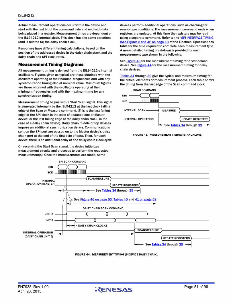
ISL94212
Actual measurement operations occur within the device and start with the last bit of the command byte and end with data being placed in a register. Measurement times are dependent on the ISL94212 internal clock. This clock has the same variations (and is related to) the daisy chain clock.
Responses have different timing calculations, based on the position of the addressed device in the daisy chain stack and the daisy chain and SPI clock rates.
Measurement Timing DiagramsAll measurement timing is derived from the ISL94212’s internal oscillators. Figures given as typical are those obtained with the oscillators operating at their nominal frequencies and with any synchronization timing also at nominal value. Maximum figures are those obtained with the oscillators operating at their minimum frequencies and with the maximum time for any synchronization timing.
Measurement timing begins with a Start Scan signal. This signal is generated internally by the ISL94212 at the last clock falling edge of the Scan or Measure command. (This is the last falling edge of the SPI clock in the case of a standalone or Master device, or the last falling edge of the daisy chain clock, in the case of a daisy chain device). Daisy chain middle or top devices impose an additional synchronization delays. Communications sent on the SPI port are passed on to the Master device’s daisy chain port at the end of the first byte of data. Then, for each device, there is an additional delay of one daisy chain clock cycle.
On receiving the Start Scan signal, the device initializes measurement circuits and proceeds to perform the requested measurement(s). Once the measurements are made, some
devices perform additional operations, such as checking for overvoltage conditions. The measurement command ends when registers are updated. At this time the registers may be read using a separate command. Refer to the “SPI INTERFACE TIMING (See Figures 2 and 3)” on page 13 of the Electrical Specifications table for the time required to complete each measurement type. A more detailed timing breakdown is provided for each measurement type shown in the following.
See Figure 43 for the measurement timing for a standalone device. See Figure 44 for the measurement timing for daisy chain devices.
Tables 34 through 39 give the typical and maximum timing for the critical elements of measurement process. Each table shows the timing from the last edge of the Scan command clock.
SCAN COMMAND
MEASURE
UPDATE REGISTERS
DIN
SCK
INTERNAL SCAN
INTERNAL OPERATION
FIGURE 43. MEASUREMENT TIMING (STANDALONE)
See Tables 34 through 39
FIGURE 44. MEASUREMENT TIMING (6 DEVICE DAISY CHAIN).
SPI SCAN COMMAND
DIN
SCK
INTERNAL OPERATION
DAISY CHAIN SCAN COMMAND
SCAN/MEASURE
UPDATE REGISTERS
INTERNAL
(DAISY CHAIN UNIT 6)
UNIT 2
UNIT 6
4 DAISY CHAIN CLOCKS
See Figure 46 on page 53, Tables 40 and 41 on page 58
OPERATION (MASTER)
See Tables 34 through 39
SCAN/MEASURE
UPDATE REGISTERS
See Tables 34 through 39
FN7938 Rev 1.00 Page 51 of 96April 23, 2015
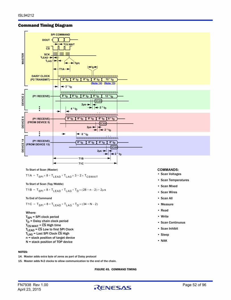
ISL94212
Command Timing Diagram
NOTES:
14. Master adds extra byte of zeros as part of Daisy protocol
15. Master adds N-2 clocks to allow communication to the end of the chain.
FIGURE 45. COMMAND TIMING
4 * tD
(P1 RECEIVE)
(P1 RECEIVE)
(P1 RECEIVE)
DE
VIC
E 6
DE
VIC
E 2
DE
VIC
E 1
4M
AS
TE
R
(FROM DEVICE 13)
To Start of Scan (Master)
To Start of Scan (Top/Middle)
To End of Command
Where:TSPI = SPI clock periodTD = Daisy chain clock periodTCS:WAIT = CS High timeTLEAD = CS Low to first SPI ClockTLAG = Last SPI Clock CS Highn = stack position of target deviceN = stack position of TOP device
T1A TSPI 8 TLEAD TLAG+ + 3 2 TCSWAIT+=
T1B TSPI 8 TLEAD TLAG TD 28 n 2–+ + + + 2s+=
T1C TSPI 8 TLEAD TLAG+ + TD 34 N 2–+ +=
DAISY CLOCK12 * tD(P2 TRANSMIT) 8* tD
12 * tD
tD
8* tD 8* tD 8* tD
8* tD 8* tD 8* tD
8* tD 8* tD
8 * tD
8* tD 8* tD 8* tD
8 * tD
2 * tD
8* tD
2µs
2µs
2µs
(FROM DEVICE 5)
2 * tD
8* tD
SCAN
2 * tD
SCAN
8* tD
8* tD
T1B
COMMANDS:• Scan Voltages
• Scan Temperatures
• Scan Mixed
• Scan Wires
• Scan All
• Measure
• Read
• Write
• Scan Continuous
• Scan Inhibit
• Sleep
• NAK
SPI COMMAND
DOUT
SCK
CS
tLEADtLAG
tCS:WAIT
tSPI
T1C
2 * tD
SCAN
(Note 14) (Note 15)
T1A
FN7938 Rev 1.00 Page 52 of 96April 23, 2015

ISL94212
Response Timing Diagrams Responses are different for Master, Middle, and Top devices. The response timings are shown in Figures 46, 47, and 48.
FIGURE 46. RESPONSE TIMING (MASTER DEVICE)
DE
VIC
E 6
DE
VIC
E 2
DE
VIC
E 1
4M
AS
TE
R
8* tD 8* tD 8* tD 4*tD
(P2 RECEIVE)
tCS
DATA READY
DIN
SCK
2µs
4 * tD
8* tD
8* tD 8* tD 8* tD 8* tD
8* tD 8* tD 8* tD 8* tD
12 * tD 8* tD 8* tD 8* tD 8* tD
Where:
TSPI = SPI clock periodTD = Daisy Chain clock periodTCS = Host delay from DATA READY Low to the CS LowTDRSP = CS High to DATA READYHighTDRWAIT = DATA READY High timeTLEAD = CS Low to first SPI ClockTLAG = Last SPI Clock CS HighN = Stack position of TOP deviceD = Number of data bytes D = 4 for one register read (or ACK/NAK response) D = 40 for read all voltages D = 22 for read all temperatures D = 22 for read all faults D = 43 for read all setup
T2 8 TSPI TDRSP TDRWAIT TCS TLEAD TLAG+ + + + + D TDRSP TD+ 42 N 2 8+–+ – 4s+=
T2
(P1 TRANSMIT)
8 * tD
(P1 TRANSMIT)
(P1 TRANSMIT)
2µs8* tD
DAISY CHAIN ACK RESPONSE
tDR:SP
tDR:WAIT
CS
tLEAD
tLAG
2*tD
2µs8 * tD
FN7938 Rev 1.00 Page 53 of 96April 23, 2015

ISL94212
NOTES:
16. Top Device adds (N - n - 1) Daisy clocks to allow communications to the targeted Middle Stack device.
17. Middle Stack Device adds (n - 2) Daisy clocks to allow communications to the Master device.
FIGURE 47. RESPONSE TIMING (MIDDLE STACK DEVICE)
Response Timing Diagrams Responses are different for Master, Middle, and Top devices. The response timings are shown in Figures 46, 47, and 48. (Continued)
tCS
DAISY CHAIN ACK RESPONSE
DE
VIC
E 6
DE
VIC
E 2
DE
VIC
E 1
4M
AS
TE
R
(P2 RECEIVE)
(P1 TRANSMIT)
(P1 TRANSMIT)
(P1 TRANSMIT)
DATA READY
DIN
SCK
(FROM DEVICE 7)
Where:
TD = Daisy Chain clock periodTSPI = SPI Clock PeriodN = Stack position of TOP devicen = Stack position of MIDDLE stack deviceTCS = Delay imposed by host from DATA READY to the first SPI clock cycleD = Number of bytes in the Middle stack device response e.g. read all cell data = 40 bytes, Register or ACK response = 4 bytes.
T3 TD 50 N n– 1–+ 4s+=
T4 TSPI 8 TCS TLEAD TLAG TDRSP TD D 8 n 2–+ + + + + + 2s+=
2µs DAISY CHAIN READ DATA RESPONSE
T3 T4
2µs
7*tD (= N - n - 1)
N
n
8* tD 8* tD 8* tD 8* tD 7* tD
8* tD 8* tD 8* tD 8* tD
8* tD
8* tD 8* tD 8* tD 4*tD
8* tD 8* tD 8* tD 8* tD
2µs
8* tD
(P2 RECEIVE)8* tD 8* tD 8* tD 8* tD
RESPONSECOMMAND
4* tD
CS
tDR:SP
tLEADtLAG
2*tD
2µs
8 * tD Note 17
Note 16
FN7938 Rev 1.00 Page 54 of 96April 23, 2015
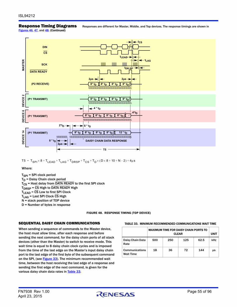
ISL94212
SEQUENTIAL DAISY CHAIN COMMUNICATIONSWhen sending a sequence of commands to the Master device, the host must allow time, after each response and before sending the next command, for the daisy chain ports of all stack devices (other than the Master) to switch to receive mode. This wait time is equal to 8 daisy chain clock cycles and is imposed from the time of the last edge on the Master’s input daisy chain port to the last edge of the first byte of the subsequent command on the SPI, (see Figure 33). The minimum recommended wait time, between the host receiving the last edge of a response and sending the first edge of the next command, is given for the various daisy chain data rates in Table 33.
FIGURE 48. RESPONSE TIMING (TOP DEVICE)
Response Timing Diagrams Responses are different for Master, Middle, and Top devices. The response timings are shown in Figures 46, 47, and 48. (Continued)
DE
VIC
E 6
DE
VIC
E 2
DE
VIC
E 1
4M
AS
TE
R
8* tD 8* tD 8* tD 4*tD
(P2 RECEIVE)
tCS
DATA READY
DIN
SCK
2µs 2µs
4 * tD
8* tD
8* tD 8* tD 8* tD 8* tD
8* tD 8* tD 8* tD 8* tD
12 * tD 8* tD 8* tD 8* tD 8* tD
Where:
TSPI = SPI clock periodTD = Daisy Chain clock periodTCS = Host delay from DATA READY to the first SPI clockTDRSP = CS High to DATA READY HighTLEAD = CS Low to first SPI ClockTLAG = Last SPI Clock CS HighN = stack position of TOP deviceD = Number of bytes in response
T5 TSPI 8 TLEAD TLAG TDRSP+ + + TCS TD D 8 10 N 2–+ + + 4s+ +=
T5
(P1 TRANSMIT)
8 * tD
(P1 TRANSMIT)
(P1 TRANSMIT)
DAISY CHAIN DATA RESPONSE
CS
tDR:SP
tLEADtLAG
2*tD
2µs8 * tD
TABLE 33. MINIMUM RECOMMENDED COMMUNICATIONS WAIT TIME
MAXIMUM TIME FOR DAISY CHAIN PORTS TO CLEAR UNIT
Daisy Chain Data Rate
500 250 125 62.5 kHz
Communications Wait Time
18 36 72 144 µs
FN7938 Rev 1.00 Page 55 of 96April 23, 2015

ISL94212
Communication and Measurement Timing TablesMeasurement Timing Tables
SCAN VOLTAGESThe Scan Voltages command initiates a sequence of measurements starting with a scan of each cell input from cell 12 to cell 1, followed by a measurement of pack voltage. Additional measurements are then performed for the internal temperature and to check the connection integrity test of the VSS and VBAT inputs. The process completes with the application of calibration parameters and the loading of registers. Table 34 shows the times after the start of scan that the cell voltage inputs are sampled. The voltages are held until the ADC completes its conversion.
SCAN TEMPERATURESThe Scan Temperatures command turns on the TEMPREG output and, after a 2.5ms settling interval, samples the ExT1 to ExT4 inputs. TEMPREG turns off on completion of the ExT4 measurement. The Reference Voltage, IC Temperature and Multiplexer loopback function are also measured. The sequence is completed with respective registers being loaded.
FIGURE 49. MINIMUM WAIT BETWEEN COMMANDS (DAISY CHAIN RESPONSE - TOP DEVICE)
DIN
SCK
UNIT 2
UNIT n
DATA READY
SPI RESPONSESPI
COMMANDNEXT SPI
COMMAND
Minimum Wait time between commands. See Table 33
TABLE 34. SCAN VOLTAGES FUNCTION TIMING - DAISY CHAIN MASTER OR STANDALONE DEVICE
EVENT TYP (µs) MAX (µs)
Sample cell 12 17 19
Sample cell 11 38 42
Sample cell 10 59 65
Sample cell 9 81 89
Sample cell 8 102 112
Sample cell 7 123 135
Sample cell 6 144 159
Sample cell 5 166 182
Sample cell 4 187 206
Sample cell 3 208 229
Sample cell 2 229 252
Sample cell 1 251 276
Complete cell voltage capture (ADC complete).Sample VBAT
304 334
Complete VBAT voltage capture 318 349
Measure internal temperature 423 465
Complete VSS test 550 605
Complete VBAT test 726 799
Load registers 766 842
TABLE 35. SCAN TEMPERATURES FUNCTION TIMING– DAISY CHAIN MASTER OR STANDALONE DEVICE
EVENT
ELAPSED TIME (µs)
TYP MAX
Turn on TEMPREG 2 2
Sample ExT1 2518 2770
~
Sample ExT4 2564 2820
Sample Reference 2584 2842
Measure Internal Temperature 2689 2958
Load registers 2689 2958
FN7938 Rev 1.00 Page 56 of 96April 23, 2015

ISL94212
SCAN MIXEDThe Scan Mixed command performs all the functions of the Scan Voltages command but interposes a measurement of the ExT1 input between the cell 7 and cell 6 measurements.
SCAN WIRESThe Scan Wires command initiates a sequence in which each input is loaded in turn with a test current for a duration of 4.5ms (default). At the end of this time the input voltage is checked and the test current is turned off. The result of each test is recorded and the Open Wire Fault and Fault Status registers are updated (data latched) at the conclusion of the tests.
SCAN ALLThe Scan All command combines the Scan Voltages, Scan Wires and Scan Temperatures commands into a single scan function.
MEASURE COMMANDSingle parameter measurements of the cell voltages, Pack Voltage, ExT1 to ExT4 inputs, IC temperature and Reference voltage are performed using the Measure command.
Command Timing TablesThe command timing tables (see Tables 40 and 41) include the time from the start of the command to the start of an internal operation and the time required for the communication to complete (since the internal operation begins before the end of the daisy chain command.)
In the case of a command that starts a scan or measurement, the host needs to wait until the command completes, by reaching the last device, plus a communications wait time (see Table 33) before sending another command. For a Read command, the response begins in the top device immediately following the end of the command.
In calculating overall timing, use the time for each target device command. This time is repeated for each device in the daisy chain, except when an “Address All” option is used. In an address all operation, use the command timing for the top device in the stack to determine when the command ends, but use the time to start of scan for each device to determine when that device begins its internal voltage sampling. For example, in a stack of six devices, it takes 86.9µs for the command to complete, but internal operations start at 7.8µs for the Master, 66.7µs for device 2, 68.9µs for device 3, etc.
TABLE 36. SCAN MIXED FUNCTION TIMING – DAISY CHAIN MASTER OR STANDALONE DEVICE
EVENT TYP (µs) MAX (µs)
Sample cell 12 17 19
Sample cell 11 38 42
Sample cell 10 59 65
Sample cell 9 80 88
Sample cell 8 101 111
Sample cell 7 122 134
Complete cell voltage capture 12-7Sample Ext1
176 194
Complete Ext1 capture 192 211
Sample cell 6 207 228
Sample cell 5 228 251
Sample cell 4 249 274
Sample cell 3 270 297
Sample cell 2 291 321
Sample cell 1 312 344
Complete cell voltage capture 6-1Sample VBAT
367 404
Complete VBAT voltage capture 381 419
Load registers 829 911
TABLE 37. SCAN WIRES FUNCTION TIMING – DAISY CHAIN MASTER OR STANDALONE DEVICE
EVENT
ELAPSED TIME (ms)
TYP MAX
Turn on VC0 current 0.03 0.05
Test VC0 4.5 5.0
Turn on VC1 current 4.6 5.1
Test VC1 9.1 10.0
~
Turn on VC12 current 54.9 60.3
Test VC12 59.4 65.3
Load registers 59.4 65.3
TABLE 38. SCAN ALL FUNCTION TIMING – DAISY CHAIN MASTER OR STANDALONE DEVICE
EVENT
ELAPSED TIME (ms)
TYP MAX
Start Scan Voltages 0 0
Start Scan Wires 0.8 0.9
Start Scan Temperatures 60.1 66.2
Complete Sequence 62.8 69.1
TABLE 39. VARIOUS MEASURE FUNCTION TIMINGS – DAISY CHAIN MASTER OR STANDALONE DEVICE
EVENT
ELAPSED TIME (µs)
TYP MAX
Measure Cell Voltage 178 196
Measure Pack Voltage 122 134
Measure ExT Input 2517 2768
Measure IC Temperature 106 116
Measure Reference Voltage 106 116
FN7938 Rev 1.00 Page 57 of 96April 23, 2015
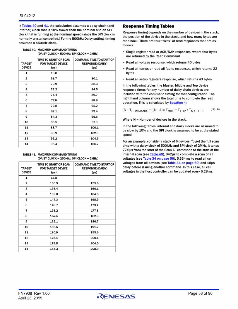
ISL94212
In Tables 40 and 41, the calculation assumes a daisy chain (and internal) clock that is 10% slower than the nominal and an SPI clock that is running at the nominal speed (since the SPI clock is normally crystal controlled.) For the 500kHz Daisy setting, timing assumes a 450kHz clock.
Response Timing TablesResponse timing depends on the number of devices in the stack, the position of the device in the stack, and how many bytes are read back. There are four “sizes” of read responses that are as follows:
• Single register read or ACK/NAK responses, where four bytes are returned by the Read Command
• Read all voltage response, which returns 40 bytes
• Read all temps or read all faults responses, which returns 22 bytes
• Read all setup registers response, which returns 43 bytes
In the following tables, the Master, Middle and Top device response times for any number of daisy chain devices are included with the command timing for that configuration. The right hand column shows the total time to complete the read operation. This is calculated by Equation 4:
Where N = Number of devices in the stack.
In the following tables, internal and daisy clocks are assumed to be slow by 10% and the SPI clock is assumed to be at the stated speed.
For an example, consider a stack of 6 devices. To get the full scan time with a daisy clock of 500kHz and SPI clock of 2MHz, it takes 77.6µs from the start of the Scan All command to the start of the internal scan (see Table 40), 842µs to complete a scan of all voltages (see Table 34 on page 56), 5.334ms to read all cell voltages from all devices (see Table 44 on page 60) and 18µs delay before issuing another command. In this case, all cell voltages in the host controller can be updated every 6.28ms.
TABLE 40. MAXIMUM COMMAND TIMING (DAISY CLOCK = 500kHz, SPI CLOCK = 2MHz)
TARGET DEVICE
TIME TO START OF SCAN FOR TARGET DEVICE
(µs)
COMMAND TIME TO START OF RESPONSE (DAISY)
(µs)
1 13.8
2 68.7 80.1
3 70.9 82.3
4 73.2 84.5
5 75.4 86.7
6 77.6 88.9
7 79.8 91.2
8 82.1 93.4
9 84.3 95.6
10 86.5 97.8
11 88.7 100.1
12 90.9 102.3
13 93.2 104.5
14 95.4 106.7
TABLE 41. MAXIMUM COMMAND TIMING (DAISY CLOCK = 250kHz, SPI CLOCK = 2MHz)
TARGET DEVICE
TIME TO START OF SCAN FOR TARGET DEVICE
(µs)
COMMAND TIME TO START OF RESPONSE (DAISY)
(µs)
1 13.8
2 130.9 155.6
3 135.4 160.1
4 139.8 164.5
5 144.3 168.9
6 148.7 173.4
7 153.2 177.8
8 157.6 182.3
9 162.1 186.7
10 166.5 191.2
11 170.9 195.6
12 175.4 200.1
13 179.8 204.5
14 184.3 208.9
N TCOMMAND N 2– TMID TTOP TMASTER+ + + (EQ. 4)
FN7938 Rev 1.00 Page 58 of 96April 23, 2015
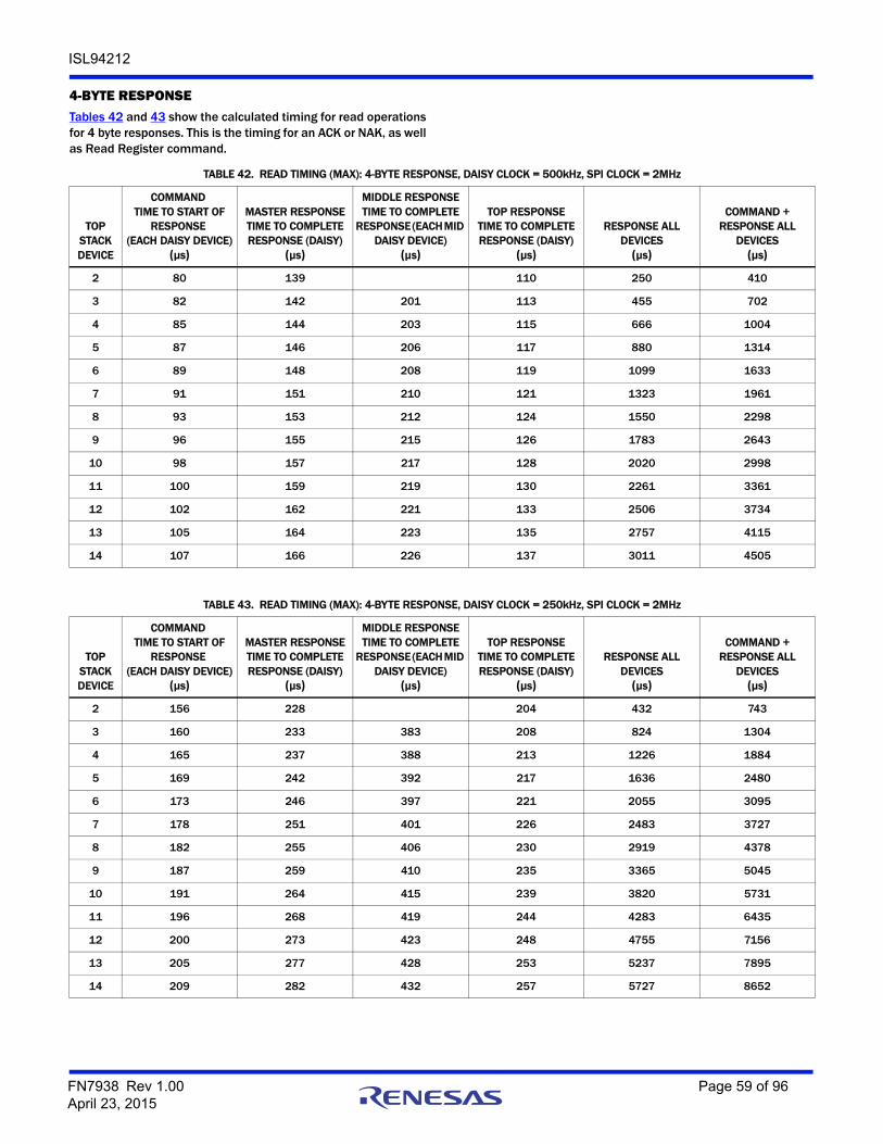
ISL94212
4-BYTE RESPONSETables 42 and 43 show the calculated timing for read operations for 4 byte responses. This is the timing for an ACK or NAK, as well as Read Register command.
TABLE 42. READ TIMING (MAX): 4-BYTE RESPONSE, DAISY CLOCK = 500kHz, SPI CLOCK = 2MHz
TOP STACK DEVICE
COMMAND TIME TO START OF
RESPONSE (EACH DAISY DEVICE)
(µs)
MASTER RESPONSETIME TO COMPLETE RESPONSE (DAISY)
(µs)
MIDDLE RESPONSETIME TO COMPLETE
RESPONSE (EACH MID DAISY DEVICE)
(µs)
TOP RESPONSETIME TO COMPLETE RESPONSE (DAISY)
(µs)
RESPONSE ALL DEVICES(µs)
COMMAND + RESPONSE ALL
DEVICES(µs)
2 80 139 110 250 410
3 82 142 201 113 455 702
4 85 144 203 115 666 1004
5 87 146 206 117 880 1314
6 89 148 208 119 1099 1633
7 91 151 210 121 1323 1961
8 93 153 212 124 1550 2298
9 96 155 215 126 1783 2643
10 98 157 217 128 2020 2998
11 100 159 219 130 2261 3361
12 102 162 221 133 2506 3734
13 105 164 223 135 2757 4115
14 107 166 226 137 3011 4505
TABLE 43. READ TIMING (MAX): 4-BYTE RESPONSE, DAISY CLOCK = 250kHz, SPI CLOCK = 2MHz
TOP STACK DEVICE
COMMAND TIME TO START OF
RESPONSE (EACH DAISY DEVICE)
(µs)
MASTER RESPONSETIME TO COMPLETE RESPONSE (DAISY)
(µs)
MIDDLE RESPONSETIME TO COMPLETE
RESPONSE (EACH MID DAISY DEVICE)
(µs)
TOP RESPONSETIME TO COMPLETE RESPONSE (DAISY)
(µs)
RESPONSE ALL DEVICES(µs)
COMMAND + RESPONSE ALL
DEVICES(µs)
2 156 228 204 432 743
3 160 233 383 208 824 1304
4 165 237 388 213 1226 1884
5 169 242 392 217 1636 2480
6 173 246 397 221 2055 3095
7 178 251 401 226 2483 3727
8 182 255 406 230 2919 4378
9 187 259 410 235 3365 5045
10 191 264 415 239 3820 5731
11 196 268 419 244 4283 6435
12 200 273 423 248 4755 7156
13 205 277 428 253 5237 7895
14 209 282 432 257 5727 8652
FN7938 Rev 1.00 Page 59 of 96April 23, 2015

ISL94212
40-BYTE RESPONSETables 44 and 45 show the calculated timing for read operations for 40-byte responses. Specifically, this is the timing for a Read All Voltages command.
TABLE 44. READ TIMING (MAX): 40-BYTE RESPONSE, DAISY CLOCK = 500kHz, SPI CLOCK = 2MHz
TOP STACK DEVICE
COMMAND TIME TO START OF
RESPONSE (EACH DAISY DEVICE)
(µs)
MASTER RESPONSETIME TO COMPLETE RESPONSE (DAISY)
(µs)
MIDDLE RESPONSETIME TO COMPLETE
RESPONSE (EACH MID DAISY DEVICE)
(µs)
TOP RESPONSETIME TO COMPLETE RESPONSE (DAISY)
(µs)
RESPONSE ALL DEVICES(µs)
COMMAND + RESPONSE ALL
DEVICES(µs)
2 80 643 750 1394 1554
3 82 646 841 753 2239 2486
4 85 648 843 755 3090 3428
5 87 650 846 757 3944 4378
6 89 652 848 759 4803 5337
7 91 655 850 761 5667 6305
8 93 657 852 764 6534 7282
9 96 659 855 766 7407 8267
10 98 661 857 768 8284 9262
11 100 663 859 770 9165 10265
12 102 666 861 773 10050 11278
13 105 668 863 775 10941 12299
14 107 670 866 777 11835 13329
TABLE 45. READ TIMING (MAX): 40-BYTE RESPONSE, DAISY CLOCK = 250kHz, SPI CLOCK = 2MHz
TOP STACK DEVICE
COMMAND TIME TO START OF
RESPONSE (EACH DAISY DEVICE)
(µs)
MASTER RESPONSETIME TO COMPLETE RESPONSE (DAISY)
(µs)
MIDDLE RESPONSETIME TO COMPLETE
RESPONSE (EACH MID DAISY DEVICE)
(µs)
TOP RESPONSETIME TO COMPLETE RESPONSE (DAISY)
(µs)
RESPONSE ALL DEVICES(µs)
COMMAND + RESPONSE ALL
DEVICES(µs)
2 156 732 1484 2216 2527
3 160 737 1663 1488 3888 4368
4 165 741 1668 1493 5570 6228
5 169 746 1672 1497 7260 8104
6 173 750 1677 1501 8959 9999
7 178 755 1681 1506 10667 11911
8 182 759 1686 1510 12383 13842
9 187 763 1690 1515 14109 15789
10 191 768 1695 1519 15844 17755
11 196 772 1699 1524 17587 19739
12 200 777 1703 1528 19339 21740
13 205 781 1708 1533 21101 23759
14 209 786 1712 1537 22871 25796
FN7938 Rev 1.00 Page 60 of 96April 23, 2015
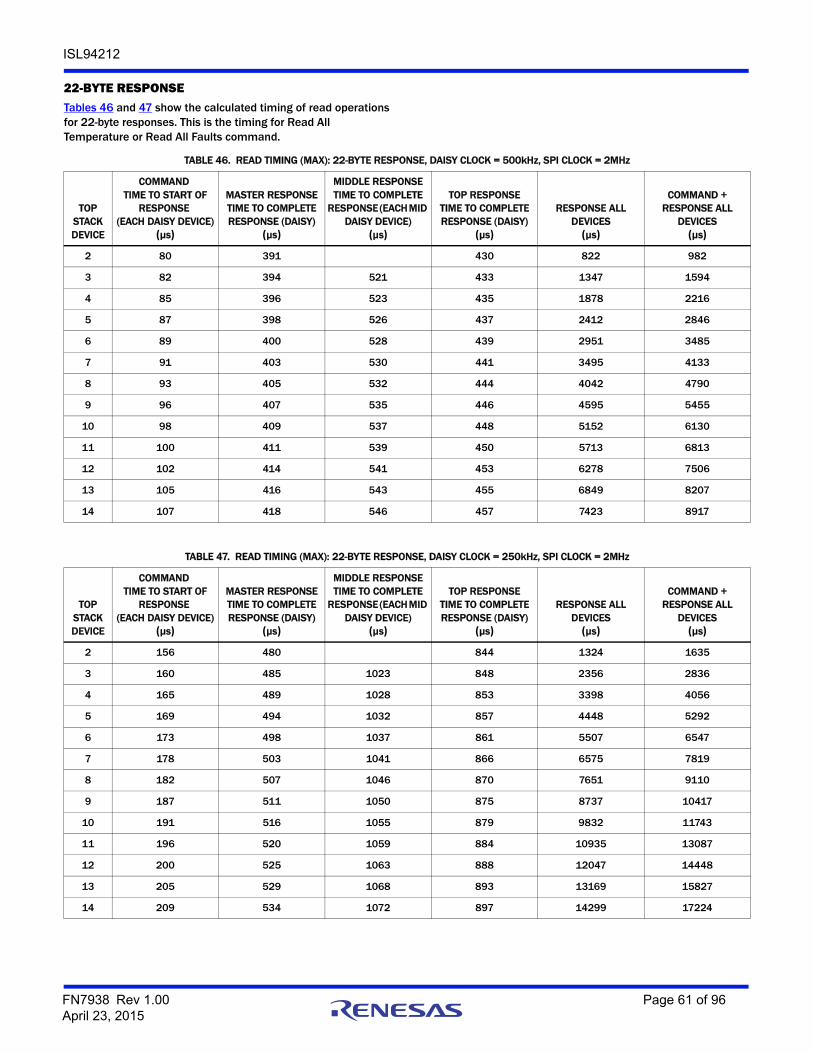
ISL94212
22-BYTE RESPONSETables 46 and 47 show the calculated timing of read operations for 22-byte responses. This is the timing for Read All Temperature or Read All Faults command.
TABLE 46. READ TIMING (MAX): 22-BYTE RESPONSE, DAISY CLOCK = 500kHz, SPI CLOCK = 2MHz
TOP STACK DEVICE
COMMAND TIME TO START OF
RESPONSE (EACH DAISY DEVICE)
(µs)
MASTER RESPONSETIME TO COMPLETE RESPONSE (DAISY)
(µs)
MIDDLE RESPONSETIME TO COMPLETE
RESPONSE (EACH MID DAISY DEVICE)
(µs)
TOP RESPONSETIME TO COMPLETE RESPONSE (DAISY)
(µs)
RESPONSE ALL DEVICES(µs)
COMMAND + RESPONSE ALL
DEVICES(µs)
2 80 391 430 822 982
3 82 394 521 433 1347 1594
4 85 396 523 435 1878 2216
5 87 398 526 437 2412 2846
6 89 400 528 439 2951 3485
7 91 403 530 441 3495 4133
8 93 405 532 444 4042 4790
9 96 407 535 446 4595 5455
10 98 409 537 448 5152 6130
11 100 411 539 450 5713 6813
12 102 414 541 453 6278 7506
13 105 416 543 455 6849 8207
14 107 418 546 457 7423 8917
TABLE 47. READ TIMING (MAX): 22-BYTE RESPONSE, DAISY CLOCK = 250kHz, SPI CLOCK = 2MHz
TOP STACK DEVICE
COMMAND TIME TO START OF
RESPONSE (EACH DAISY DEVICE)
(µs)
MASTER RESPONSETIME TO COMPLETE RESPONSE (DAISY)
(µs)
MIDDLE RESPONSETIME TO COMPLETE
RESPONSE (EACH MID DAISY DEVICE)
(µs)
TOP RESPONSETIME TO COMPLETE RESPONSE (DAISY)
(µs)
RESPONSE ALL DEVICES(µs)
COMMAND + RESPONSE ALL
DEVICES(µs)
2 156 480 844 1324 1635
3 160 485 1023 848 2356 2836
4 165 489 1028 853 3398 4056
5 169 494 1032 857 4448 5292
6 173 498 1037 861 5507 6547
7 178 503 1041 866 6575 7819
8 182 507 1046 870 7651 9110
9 187 511 1050 875 8737 10417
10 191 516 1055 879 9832 11743
11 196 520 1059 884 10935 13087
12 200 525 1063 888 12047 14448
13 205 529 1068 893 13169 15827
14 209 534 1072 897 14299 17224
FN7938 Rev 1.00 Page 61 of 96April 23, 2015
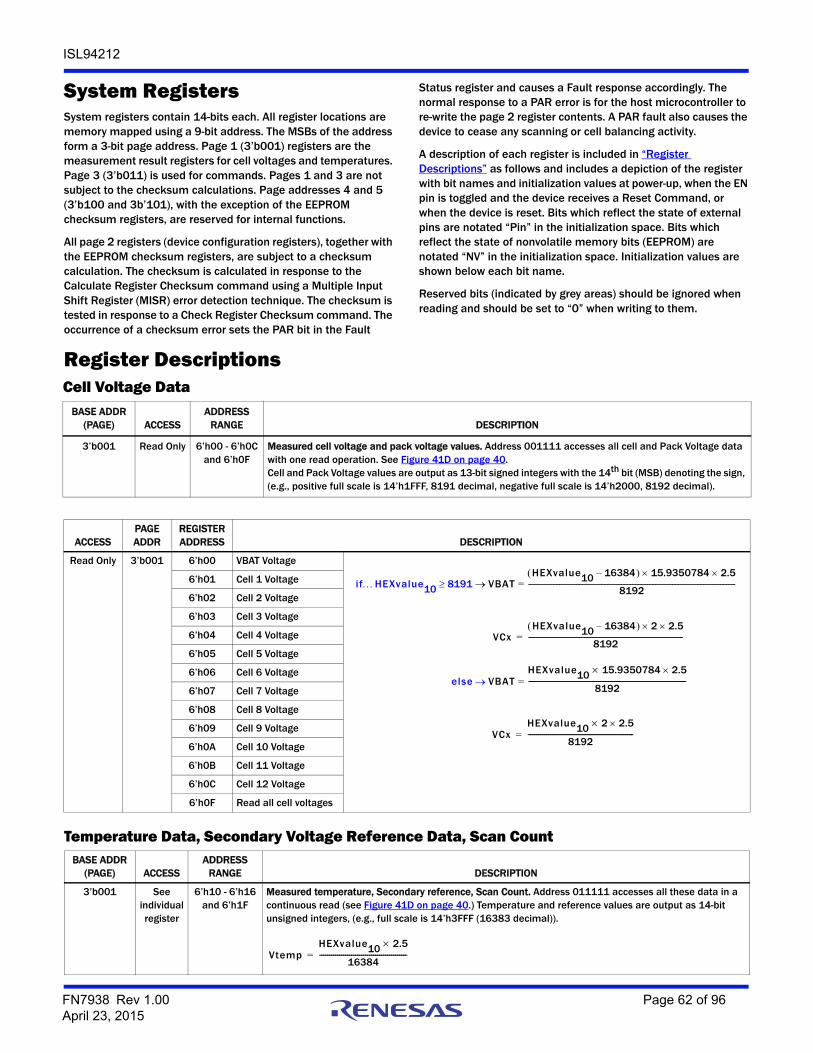
ISL94212
System RegistersSystem registers contain 14-bits each. All register locations are memory mapped using a 9-bit address. The MSBs of the address form a 3-bit page address. Page 1 (3’b001) registers are the measurement result registers for cell voltages and temperatures. Page 3 (3’b011) is used for commands. Pages 1 and 3 are not subject to the checksum calculations. Page addresses 4 and 5 (3’b100 and 3b’101), with the exception of the EEPROM checksum registers, are reserved for internal functions.
All page 2 registers (device configuration registers), together with the EEPROM checksum registers, are subject to a checksum calculation. The checksum is calculated in response to the Calculate Register Checksum command using a Multiple Input Shift Register (MISR) error detection technique. The checksum is tested in response to a Check Register Checksum command. The occurrence of a checksum error sets the PAR bit in the Fault
Status register and causes a Fault response accordingly. The normal response to a PAR error is for the host microcontroller to re-write the page 2 register contents. A PAR fault also causes the device to cease any scanning or cell balancing activity.
A description of each register is included in “Register Descriptions” as follows and includes a depiction of the register with bit names and initialization values at power-up, when the EN pin is toggled and the device receives a Reset Command, or when the device is reset. Bits which reflect the state of external pins are notated “Pin” in the initialization space. Bits which reflect the state of nonvolatile memory bits (EEPROM) are notated “NV” in the initialization space. Initialization values are shown below each bit name.
Reserved bits (indicated by grey areas) should be ignored when reading and should be set to “0” when writing to them.
Register DescriptionsCell Voltage Data
BASE ADDR (PAGE) ACCESS
ADDRESS RANGE DESCRIPTION
3’b001 Read Only 6’h00 - 6’h0Cand 6’h0F
Measured cell voltage and pack voltage values. Address 001111 accesses all cell and Pack Voltage data with one read operation. See Figure 41D on page 40.Cell and Pack Voltage values are output as 13-bit signed integers with the 14th bit (MSB) denoting the sign, (e.g., positive full scale is 14’h1FFF, 8191 decimal, negative full scale is 14’h2000, 8192 decimal).
ACCESSPAGE ADDR
REGISTER ADDRESS DESCRIPTION
Read Only 3’b001 6’h00 VBAT Voltage
6’h01 Cell 1 Voltage
6’h02 Cell 2 Voltage
6’h03 Cell 3 Voltage
6’h04 Cell 4 Voltage
6’h05 Cell 5 Voltage
6’h06 Cell 6 Voltage
6’h07 Cell 7 Voltage
6’h08 Cell 8 Voltage
6’h09 Cell 9 Voltage
6’h0A Cell 10 Voltage
6’h0B Cell 11 Voltage
6’h0C Cell 12 Voltage
6’h0F Read all cell voltages
ifHEXvalue10 8191 VBATHEXvalue10 16384– 15.9350784 2.5
8192--------------------------------------------------------------------------------------------------------------------------------------=
VCxHEXvalue10 16384– 2 2.5
8192----------------------------------------------------------------------------------------------------=
else VBATHEXvalue10 15.9350784 2.5
8192-------------------------------------------------------------------------------=
VCxHEXvalue10 2 2.5
8192-----------------------------------------------------=
Temperature Data, Secondary Voltage Reference Data, Scan CountBASE ADDR
(PAGE) ACCESSADDRESS
RANGE DESCRIPTION
3’b001 See individual register
6’h10 - 6’h16and 6’h1F
Measured temperature, Secondary reference, Scan Count. Address 011111 accesses all these data in a continuous read (see Figure 41D on page 40.) Temperature and reference values are output as 14-bit unsigned integers, (e.g., full scale is 14’h3FFF (16383 decimal)).
VtempHEXvalue10 2.5
16384--------------------------------------------=
FN7938 Rev 1.00 Page 62 of 96April 23, 2015
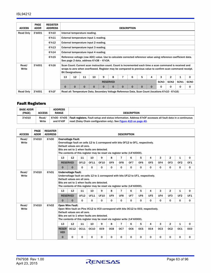
ISL94212
ACCESSPAGE ADDR
REGISTER ADDRESS DESCRIPTION
Read Only 3’b001 6’h10 Internal temperature reading.
6’h11 External temperature input 1 reading.
6’h12 External temperature input 2 reading.
6’h13 External temperature input 3 reading.
6’h14 External temperature input 4 reading.
6’h15 Reference voltage (raw ADC) value. Use to calculate corrected reference value using reference coefficient data. See page 2 data, address 6’h38 – 6’h3A.
Read/Write
3’h001 6’h16 Scan Count: Current scan instruction count. Count is incremented each time a scan command is received and wraps to zero when overflowed. Register may be compared to previous value to confirm scan command receipt.Bit Designations:
13 12 11 10 9 8 7 6 5 4 3 2 1 0
RESERVED SCN3 SCN2 SCN1 SCN0
0 0 0 0 0 0 0 0 0 0 0 0 0 0
Read Only 3’h001 6’h1F Read all: Temperature Data, Secondary Voltage Reference Data, Scan Count (locations 6’h10 - 6’h16)
Fault RegistersBASE ADDR
(PAGE) ACCESSADDRESS
RANGE DESCRIPTION
3’h010 Read/Write
6’h00 - 6’h05and 6’h0F
Fault registers. Fault setup and status information. Address 6’h0F accesses all fault data in a continuous read (Daisy Chain configuration only). See Figure 41D on page 40.
ACCESSPAGE ADDR
REGISTER ADDRESS DESCRIPTION
Read/Write
3’h010 6’h00 Overvoltage Fault: Overvoltage fault on cells 12 to 1 correspond with bits OF12 to OF1, respectively. Default values are all zero. Bits are set to 1 when faults are detected. The contents of this register may be reset via register write (14’h0000).
13 12 11 10 9 8 7 6 5 4 3 2 1 0
RESERVED OF12 OF11 OF10 OF9 OF8 OF7 OF6 OF5 OF4 OF3 OF2 OF1
0 0 0 0 0 0 0 0 0 0 0 0 0 0
Read/Write
3’h010 6’h01 Undervoltage Fault: Undervoltage fault on cells 12 to 1 correspond with bits UF12 to UF1, respectively. Default values are all zero. Bits are set to 1 when faults are detected. The contents of this register may be reset via register write (14’h0000).
13 12 11 10 9 8 7 6 5 4 3 2 1 0
RESERVED UF12 UF11 UF10 UF9 UF8 UF7 UF6 UF5 UF4 UF3 UF2 UF1
0 0 0 0 0 0 0 0 0 0 0 0 0 0
Read/Write
3’h010 6’h02 Open Wire Fault: Open Wire fault on Pins VC12 to VC0 correspond with bits OC12 to OC0, respectively. Default values are all zero. Bits are set to 1 when faults are detected. The contents of this register may be reset via register write (14’h0000).
13 12 11 10 9 8 7 6 5 4 3 2 1 0
RESERVED
OC12 OC11 OC10 OC9 OC8 OC7 OC6 OC5 OC4 OC3 OC2 OC1 OC0
0 0 0 0 0 0 0 0 0 0 0 0 0 0
FN7938 Rev 1.00 Page 63 of 96April 23, 2015
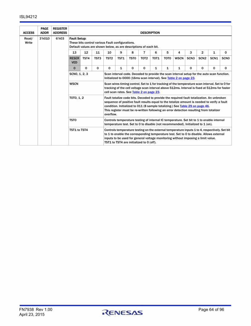
ISL94212
Read/Write
3’h010 6’h03 Fault Setup: These bits control various Fault configurations. Default values are shown below, as are descriptions of each bit.
13 12 11 10 9 8 7 6 5 4 3 2 1 0
RESERVED
TST4 TST3 TST2 TST1 TST0 TOT2 TOT1 TOT0 WSCN SCN3 SCN2 SCN1 SCN0
0 0 0 0 1 0 0 1 1 1 0 0 0 0
SCN0, 1, 2, 3 Scan interval code. Decoded to provide the scan interval setup for the auto scan function. Initialized to 0000 (16ms scan interval). See Table 2 on page 23.
WSCN Scan wires timing control. Set to 1 for tracking of the temperature scan interval. Set to 0 for tracking of the cell voltage scan interval above 512ms. Interval is fixed at 512ms for faster cell scan rates. See Table 2 on page 23.
TOT0, 1, 2 Fault totalize code bits. Decoded to provide the required fault totalization. An unbroken sequence of positive fault results equal to the totalize amount is needed to verify a fault condition. Initialized to 011 (8 sample totalizing.) See Table 29 on page 46.This register must be re-written following an error detection resulting from totalizer overflow.
TST0 Controls temperature testing of internal IC temperature. Set bit to 1 to enable internal temperature test. Set to 0 to disable (not recommended). Initialized to 1 (on).
TST1 to TST4 Controls temperature testing on the external temperature inputs 1 to 4, respectively. Set bit to 1 to enable the corresponding temperature test. Set to 0 to disable. Allows external inputs to be used for general voltage monitoring without imposing a limit value. TST1 to TST4 are initialized to 0 (off).
ACCESSPAGE ADDR
REGISTER ADDRESS DESCRIPTION
FN7938 Rev 1.00 Page 64 of 96April 23, 2015

ISL94212
Read/Write
3’h010 6’h04 Fault Status: The FAULT logic output is an OR function of the bits in this register: the output will be asserted low if any bits in the Fault Status register are set.
13 12 11 10 9 8 7 6 5 4 3 2 1 0
MUX REG REF PAR OVSS OVBAT OW UV OV OT WDGF OSC RESERVED
0 0 0 0 0 0 0 0 0 0 0 0 0 0
OSC Oscillator fault bit. Bit is set in response to a fault on either the 4MHz or 32kHz oscillators. Note that communications functions may be disrupted by a fault in the 4MHz oscillator.
WDGF Watchdog timeout fault. Bit is set in response to a watchdog timeout.
OT Over-temperature fault. ‘OR’ of over-temperature fault bits: TFLT0 to TFLT4. This bit is latched. The bits in the Over-temperature Fault register must first be reset before this bit can be reset. Reset by writing 14’h0000 to this register.
OV Overvoltage fault. ‘OR’ of Overvoltage fault bits: OF1 to OF12. This bit is latched. The bits in the Overvoltage Fault register must first be reset before this bit can be reset. Reset by writing 14’h0000 to this register.
UV Undervoltage fault. ‘OR’ of Undervoltage fault bits: UF1 to UF12. This bit is latched. The bits in the Undervoltage Fault register must first be reset before this bit can be reset. Reset by writing 14’h0000 to this register.
OW Open Wire fault. ‘OR’ of open wire fault bits: OC0 to OC12. This bit is latched. The bits in the Open Wire Fault register must first be reset before this bit can be reset. Reset by writing 14’h0000 to this register.
OVBAT Open wire fault on VBAT connection. Bit set to 1 when a fault is detected. May be reset via register write (14’h0000).
OVSS Open wire fault on VSS connection. Bit set to 1 when a fault is detected. May be reset via register write (14’h0000).
PAR Register checksum (Parity) error. This bit is set in response to a register checksum error. The checksum is calculated and stored in response to a Calc Register Checksum command and acts on the contents of all page 2 registers. The Check Register Checksum command is used to repeat the calculation and compare the results to the stored value. The PAR bit is then set if the two results are not equal. This bit is not set in response to a nonvolatile EEPROM memory checksum error. See table on page 71.
REF Voltage reference fault. This bit is set if the voltage reference value is outside its “power-good” range.
REG Voltage regulator fault. This bit is set if a voltage regulator value (V3P3, VCC or V2P5) is outside its “power-good” range.
MUX Temperature multiplexer error. This bit is set if the VCC loopback check returns a fault. The VCC loopback check is performed at the end of each temperature scan.
Read/Write
3’h010 6’h05 Cell Setup: Default values are shown below, as are descriptions of each bit.
13 12 11 10 9 8 7 6 5 4 3 2 1 0
FFSN FFSP C12 C11 C10 C9 C8 C7 C6 C5 C4 C3 C2 C1
0 0 0 0 0 0 0 0 0 0 0 0 0 0
C1 to C12 Enable/disable cell overvoltage, undervoltage and open wire detection on cell 1 to 12, respectively. Set to 1 to disable OV/UV and open wire tests.
FFSP Force ADC input to Full Scale Positive. All cell scan readings forced to 14'h1FFF. All temperature scan readings forced to 14'h3FFF.
FFSN Force ADC input to Full Scale Negative. All cell scan readings forced to 14'h2000. All temperature scan readings forced to 14'h0000.
NOTE: The ADC input functions normally if both FFSN and FFSP are set to '1' but this setting is not supported.
ACCESSPAGE ADDR
REGISTER ADDRESS DESCRIPTION
FN7938 Rev 1.00 Page 65 of 96April 23, 2015
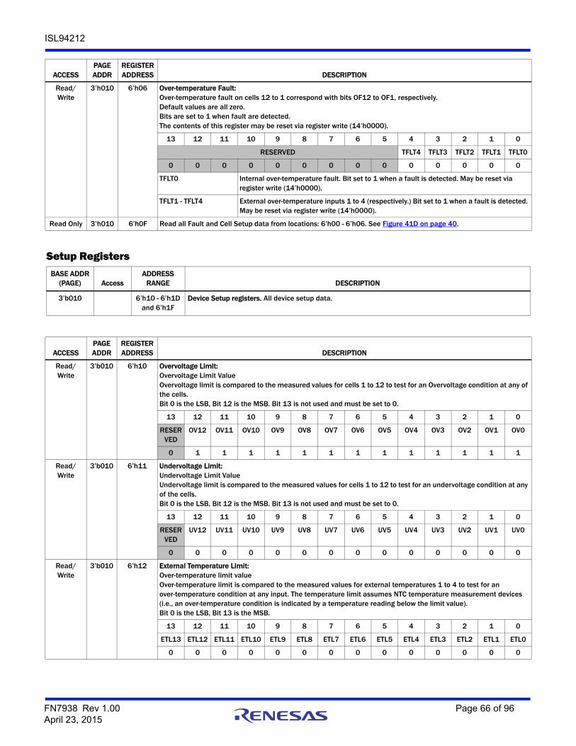
ISL94212
Read/Write
3’h010 6’h06 Over-temperature Fault: Over-temperature fault on cells 12 to 1 correspond with bits OF12 to OF1, respectively. Default values are all zero. Bits are set to 1 when fault are detected. The contents of this register may be reset via register write (14’h0000).
13 12 11 10 9 8 7 6 5 4 3 2 1 0
RESERVED TFLT4 TFLT3 TFLT2 TFLT1 TFLT0
0 0 0 0 0 0 0 0 0 0 0 0 0 0
TFLT0 Internal over-temperature fault. Bit set to 1 when a fault is detected. May be reset via register write (14’h0000).
TFLT1 - TFLT4 External over-temperature inputs 1 to 4 (respectively.) Bit set to 1 when a fault is detected. May be reset via register write (14’h0000).
Read Only 3’h010 6’h0F Read all Fault and Cell Setup data from locations: 6’h00 - 6’h06. See Figure 41D on page 40.
ACCESSPAGE ADDR
REGISTER ADDRESS DESCRIPTION
Setup RegistersBASE ADDR
(PAGE) AccessADDRESS
RANGE DESCRIPTION
3’b010 6’h10 - 6’h1Dand 6’h1F
Device Setup registers. All device setup data.
ACCESSPAGE ADDR
REGISTER ADDRESS DESCRIPTION
Read/Write
3’b010 6’h10 Overvoltage Limit: Overvoltage Limit Value Overvoltage limit is compared to the measured values for cells 1 to 12 to test for an Overvoltage condition at any of the cells.Bit 0 is the LSB, Bit 12 is the MSB. Bit 13 is not used and must be set to 0.
13 12 11 10 9 8 7 6 5 4 3 2 1 0
RESERVED
OV12 OV11 OV10 OV9 OV8 OV7 OV6 OV5 OV4 OV3 OV2 OV1 OV0
0 1 1 1 1 1 1 1 1 1 1 1 1 1
Read/Write
3’b010 6’h11 Undervoltage Limit: Undervoltage Limit Value Undervoltage limit is compared to the measured values for cells 1 to 12 to test for an undervoltage condition at any of the cells.Bit 0 is the LSB, Bit 12 is the MSB. Bit 13 is not used and must be set to 0.
13 12 11 10 9 8 7 6 5 4 3 2 1 0
RESERVED
UV12 UV11 UV10 UV9 UV8 UV7 UV6 UV5 UV4 UV3 UV2 UV1 UV0
0 0 0 0 0 0 0 0 0 0 0 0 0 0
Read/Write
3’b010 6’h12 External Temperature Limit: Over-temperature limit value Over-temperature limit is compared to the measured values for external temperatures 1 to 4 to test for an over-temperature condition at any input. The temperature limit assumes NTC temperature measurement devices (i.e., an over-temperature condition is indicated by a temperature reading below the limit value).Bit 0 is the LSB, Bit 13 is the MSB.
13 12 11 10 9 8 7 6 5 4 3 2 1 0
ETL13 ETL12 ETL11 ETL10 ETL9 ETL8 ETL7 ETL6 ETL5 ETL4 ETL3 ETL2 ETL1 ETL0
0 0 0 0 0 0 0 0 0 0 0 0 0 0
FN7938 Rev 1.00 Page 66 of 96April 23, 2015
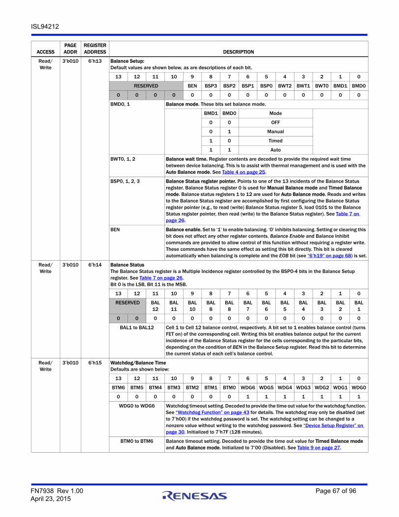
ISL94212
Read/Write
3’b010 6’h13 Balance Setup: Default values are shown below, as are descriptions of each bit.
13 12 11 10 9 8 7 6 5 4 3 2 1 0
RESERVED BEN BSP3 BSP2 BSP1 BSP0 BWT2 BWT1 BWT0 BMD1 BMD0
0 0 0 0 0 0 0 0 0 0 0 0 0 0
BMD0, 1 Balance mode. These bits set balance mode.
BMD1 BMD0 Mode
0 0 OFF
0 1 Manual
1 0 Timed
1 1 Auto
BWT0, 1, 2 Balance wait time. Register contents are decoded to provide the required wait time between device balancing. This is to assist with thermal management and is used with the Auto Balance mode. See Table 4 on page 25.
BSP0, 1, 2, 3 Balance Status register pointer. Points to one of the 13 incidents of the Balance Status register. Balance Status register 0 is used for Manual Balance mode and Timed Balance mode. Balance status registers 1 to 12 are used for Auto Balance mode. Reads and writes to the Balance Status register are accomplished by first configuring the Balance Status register pointer (e.g., to read (write) Balance Status register 5, load 0101 to the Balance Status register pointer, then read (write) to the Balance Status register). See Table 7 on page 26.
BEN Balance enable. Set to ‘1’ to enable balancing. ‘0’ inhibits balancing. Setting or clearing this bit does not affect any other register contents. Balance Enable and Balance Inhibit commands are provided to allow control of this function without requiring a register write. These commands have the same effect as setting this bit directly. This bit is cleared automatically when balancing is complete and the EOB bit (see “6’h19” on page 68) is set.
Read/Write
3’b010 6’h14 Balance StatusThe Balance Status register is a Multiple Incidence register controlled by the BSP0-4 bits in the Balance Setup register. See Table 7 on page 26.Bit 0 is the LSB, Bit 11 is the MSB.
13 12 11 10 9 8 7 6 5 4 3 2 1 0
RESERVED BAL12
BAL11
BAL10
BAL8
BAL8
BAL7
BAL6
BAL5
BAL4
BAL3
BAL2
BAL1
0 0 0 0 0 0 0 0 0 0 0 0 0 0
BAL1 to BAL12 Cell 1 to Cell 12 balance control, respectively. A bit set to 1 enables balance control (turns FET on) of the corresponding cell. Writing this bit enables balance output for the current incidence of the Balance Status register for the cells corresponding to the particular bits, depending on the condition of BEN in the Balance Setup register. Read this bit to determine the current status of each cell’s balance control.
Read/Write
3’b010 6’h15 Watchdog/Balance TimeDefaults are shown below:
13 12 11 10 9 8 7 6 5 4 3 2 1 0
BTM6 BTM5 BTM4 BTM3 BTM2 BTM1 BTM0 WDG6 WDG5 WDG4 WDG3 WDG2 WDG1 WDG0
0 0 0 0 0 0 0 1 1 1 1 1 1 1
WDG0 to WDG6 Watchdog timeout setting. Decoded to provide the time out value for the watchdog function. See “Watchdog Function” on page 43 for details. The watchdog may only be disabled (set to 7’h00) if the watchdog password is set. The watchdog setting can be changed to a nonzero value without writing to the watchdog password. See “Device Setup Register” on page 30. Initialized to 7’h7F (128 minutes).
BTM0 to BTM6 Balance timeout setting. Decoded to provide the time out value for Timed Balance mode and Auto Balance mode. Initialized to 7’00 (Disabled). See Table 9 on page 27.
ACCESSPAGE ADDR
REGISTER ADDRESS DESCRIPTION
FN7938 Rev 1.00 Page 67 of 96April 23, 2015
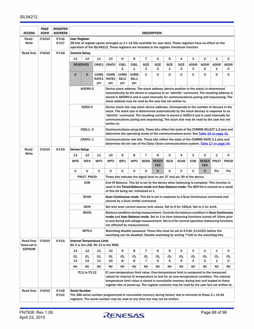
ISL94212
Read/Write
3’b010 6’h166’h17
User Register28 bits of register space arranged as 2 x 14 bits available for user data. These registers have no effect on the operation of the ISL94212. These registers are included in the register checksum function.
Read Only 3’b010 6’h18 Comms Setup
13 12 11 10 9 8 7 6 5 4 3 2 1 0
RESERVED CRAT1 CRAT0 CSEL2
CSEL1
SIZE3
SIZE2
SIZE1
SIZE0
ADDR3
ADDR2
ADDR1
ADDR0
0 0 COMS RATE1
pin
COMS RATE0
pin
COMS SEL2 pin
COMS SEL1 pin
0 0 0 0 0 0 0 0
ADDR0-3 Device stack address. The stack address (device position in the stack) is determined automatically by the device in response to an “Identify” command. The resulting address is stored in ADDR0-3 and is used internally for communications paring and sequencing. The stack address may be read by the user but not written to.
SIZE0-3 Device stack size (top stack device address). Corresponds to the number of devices in the stack. The stack size is determined automatically by the stack devices in response to an “Identify” command. The resulting number is stored in SIZE0-3 and is used internally for communications paring and sequencing. The stack size may be read by the user but not written to.
CSEL1, 2 Communications setup bits. These bits reflect the state of the COMMS SELECT 1,2 pins and determine the operating mode of the communications ports. See Table 15 on page 31.
CRAT0, 1 Communications rate bits. These bits reflect the state of the COMMS RATE 0,1 pins and determine the bit rate of the Daisy Chain communications system. Table 17 on page 34.
Read/Write
3’b010 6’h19 Device Setup
13 12 11 10 9 8 7 6 5 4 3 2 1 0
WP5 WP4 WP3 WP2 WP1 WP0 BDDS RESERVED
ISCN SCAN EOB RESERVED
PIN37 PIN39
0 0 0 0 0 0 0 0 0 0 0 0 Pin Pin
PIN37, PIN39 These bits indicate the signal level on pin 37 and pin 39 of the device.
EOB End Of Balance. This bit is set by the device when balancing is complete. This function is used in the Timed Balance mode and Auto Balance mode. The BEN bit is cleared as a result of this bit being set. Initialized to 1.
SCAN Scan Continuous mode. This bit is set in response to a Scan Continuous command and cleared by a Scan Inhibit command.
ISCN Set wire scan current source/sink values. Set to 0 for 150µA. Set to 1 for 1mA.
BDDS Balance condition during measurement. Controls the balance condition in Scan Continuous mode and Auto Balance mode. Set to 1 to have balancing functions turned off 10ms prior to and during cell voltage measurement. Set to 0 for normal operation (balancing functions not affected by measurement).
WP5:0 Watchdog disable password. These bits must be set to 6’h3A (111010) before the watchdog can be disabled. Disable watchdog by writing 7’h00 to the watchdog bits.
Read OnlyValue set in
EEPROM
3’b010 6’h1A Internal Temperature LimitBit 0 is the LSB, Bit 13 is the MSB.
13 12 11 10 9 8 7 6 5 4 3 2 1 0
ITL13
ITL12
ITL11
ITL10
ITL8
ITL8
ITL7
ITL6
ITL5
ITL4
ITL3
ITL2
ITL1
ITL0
NV NV NV NV NV NV NV NV NV NV NV NV NV NV
ITL1 to ITL12 IC over-temperature limit value. Over-temperature limit is compared to the measured values for internal IC temperature to test for an over-temperature condition. The internal temperature limit value is stored in nonvolatile memory during test and loaded to these register bits at power-up. The register contents may be read by the user but not written to.
Read Only 3’b010 6’h1B6’h1C
Serial NumberThe 28b serial number programmed in nonvolatile memory during factory test is mirrored to these 2 x 14 bit registers. The serial number may be read at any time but may not be written.
ACCESSPAGE ADDR
REGISTER ADDRESS DESCRIPTION
FN7938 Rev 1.00 Page 68 of 96April 23, 2015
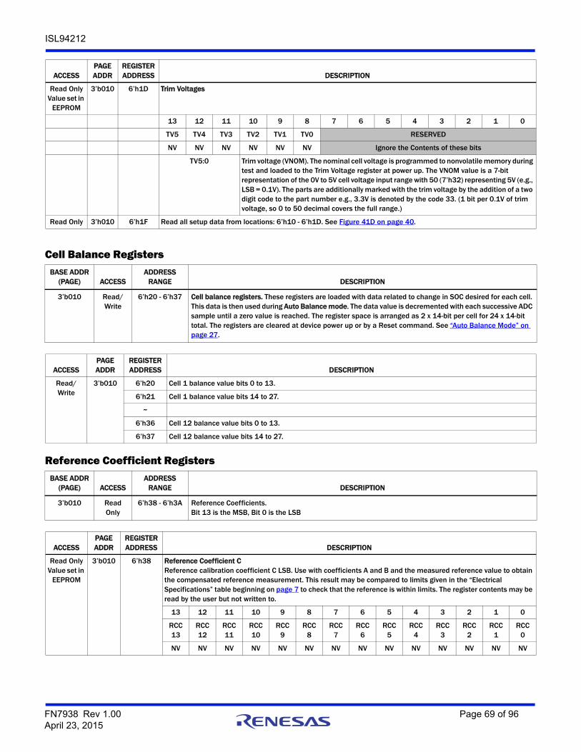
ISL94212
Read OnlyValue set in
EEPROM
3’b010 6’h1D Trim Voltages
13 12 11 10 9 8 7 6 5 4 3 2 1 0
TV5 TV4 TV3 TV2 TV1 TV0 RESERVED
NV NV NV NV NV NV Ignore the Contents of these bits
TV5:0 Trim voltage (VNOM). The nominal cell voltage is programmed to nonvolatile memory during test and loaded to the Trim Voltage register at power up. The VNOM value is a 7-bit representation of the 0V to 5V cell voltage input range with 50 (7’h32) representing 5V (e.g., LSB = 0.1V). The parts are additionally marked with the trim voltage by the addition of a two digit code to the part number e.g., 3.3V is denoted by the code 33. (1 bit per 0.1V of trim voltage, so 0 to 50 decimal covers the full range.)
Read Only 3’h010 6’h1F Read all setup data from locations: 6’h10 - 6’h1D. See Figure 41D on page 40.
ACCESSPAGE ADDR
REGISTER ADDRESS DESCRIPTION
Cell Balance RegistersBASE ADDR
(PAGE) ACCESSADDRESS
RANGE DESCRIPTION
3’b010 Read/Write
6’h20 - 6’h37 Cell balance registers. These registers are loaded with data related to change in SOC desired for each cell. This data is then used during Auto Balance mode. The data value is decremented with each successive ADC sample until a zero value is reached. The register space is arranged as 2 x 14-bit per cell for 24 x 14-bit total. The registers are cleared at device power up or by a Reset command. See “Auto Balance Mode” on page 27.
ACCESSPAGEADDR
REGISTER ADDRESS DESCRIPTION
Read/Write
3’b010 6’h20 Cell 1 balance value bits 0 to 13.
6’h21 Cell 1 balance value bits 14 to 27.
~
6’h36 Cell 12 balance value bits 0 to 13.
6’h37 Cell 12 balance value bits 14 to 27.
Reference Coefficient RegistersBASE ADDR
(PAGE) ACCESSADDRESS
RANGE DESCRIPTION
3’b010 Read Only
6’h38 - 6’h3A Reference Coefficients.Bit 13 is the MSB, Bit 0 is the LSB
ACCESSPAGE ADDR
REGISTER ADDRESS DESCRIPTION
Read OnlyValue set in
EEPROM
3’b010 6’h38 Reference Coefficient CReference calibration coefficient C LSB. Use with coefficients A and B and the measured reference value to obtain the compensated reference measurement. This result may be compared to limits given in the “Electrical Specifications” table beginning on page 7 to check that the reference is within limits. The register contents may be read by the user but not written to.
13 12 11 10 9 8 7 6 5 4 3 2 1 0
RCC13
RCC12
RCC11
RCC10
RCC9
RCC8
RCC7
RCC6
RCC5
RCC4
RCC3
RCC2
RCC1
RCC0
NV NV NV NV NV NV NV NV NV NV NV NV NV NV
FN7938 Rev 1.00 Page 69 of 96April 23, 2015

ISL94212
Read Only 3’b010 6’h39 Reference Coefficient BReference calibration coefficient B LSB. Use with coefficients A and C and the measured reference value to obtain the compensated reference measurement. This result may be compared to limits given in the “Electrical Specifications” table beginning on page 7 to check that the reference is within limits. The register contents may be read by the user but not written to.
13 12 11 10 9 8 7 6 5 4 3 2 1 0
RCB13
RCB12
RCB11
RCB10
RCB9
RCB8
RCB7
RCB6
RCB5
RCB4
RCB3
RCB2
RCB1
RCB0
NV NV NV NV NV NV NV NV NV NV NV NV NV NV
Read Only 3’b010 6’h3A Reference Coefficient AReference calibration coefficient A LSB. Use with coefficients B and C and the measured reference value to obtain the compensated reference measurement. This result may be compared to limits given in the “Electrical Specifications” table beginning on page 7 to check that the reference is within limits. The register contents may be read by the user but not written to.
13 12 11 10 9 8 7 6 5 4 3 2 1 0
RCA8
RCA7
RCA6
RCA5
RCA4
RCA3
RCA2
RCA1
RCA0
RESERVED
NV NV NV NV NV NV NV NV NV Ignore the content of these bits
ACCESSPAGE ADDR
REGISTER ADDRESS DESCRIPTION
Cells In Balance RegisterBASE ADDR
(PAGE) ACCESSADDRESS
RANGE DESCRIPTION
3’b010 Read Only
6’h3B Cells In balance (valid for non-daisy chain configuration only).
ACCESSPAGE ADDR
REGISTER ADDRESS DESCRIPTION
Read Only 3’b010 6’h3B Cells Balance EnabledThis register reports the current condition of the cell balance outputs.Bit 0 is the LSB, Bit 11 is the MSB.
13 12 11 10 9 8 7 6 5 4 3 2 1 0
RESERVED CBEN12
CBEN11
CBEN10
CBEN8
CBEN8
CBEN7
CBEN6
CBEN5
CBEN4
CBEN3
CBEN2
CBEN1
0 0 0 0 0 0 0 0 0 0 0 0 0 0
BALI1 to BALI12 Indicates the current balancing status of cell 1 to cell 12 (respectively). “1” indicates balancing is enabled for this cell. “0” indicates that balancing is turned off.
Device CommandsBASE ADDR
(PAGE) ACCESSADDRESS
RANGE DESCRIPTION
3’b011 Read Only
6’h01 - 6’h14 Device commands. Actions and communications administration. Not physical registers but memory mapped device commands. Commands from host and device responses are all configured as reads (BASE ADDR MSB = 0). Write operations breaks the communication rules and produce NAK from the target device.
FN7938 Rev 1.00 Page 70 of 96April 23, 2015
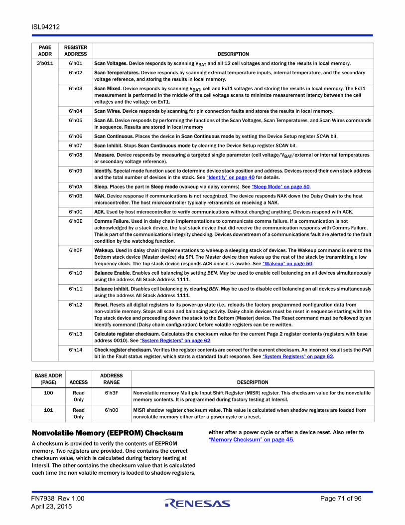
ISL94212
Nonvolatile Memory (EEPROM) ChecksumA checksum is provided to verify the contents of EEPROM memory. Two registers are provided. One contains the correct checksum value, which is calculated during factory testing at Intersil. The other contains the checksum value that is calculated each time the non volatile memory is loaded to shadow registers,
either after a power cycle or after a device reset. Also refer to “Memory Checksum” on page 45.
PAGEADDR
REGISTER ADDRESS DESCRIPTION
3’b011 6’h01 Scan Voltages. Device responds by scanning VBAT and all 12 cell voltages and storing the results in local memory.
6’h02 Scan Temperatures. Device responds by scanning external temperature inputs, internal temperature, and the secondary voltage reference, and storing the results in local memory.
6’h03 Scan Mixed. Device responds by scanning VBAT, cell and ExT1 voltages and storing the results in local memory. The ExT1 measurement is performed in the middle of the cell voltage scans to minimize measurement latency between the cell voltages and the voltage on ExT1.
6’h04 Scan Wires. Device responds by scanning for pin connection faults and stores the results in local memory.
6’h05 Scan All. Device responds by performing the functions of the Scan Voltages, Scan Temperatures, and Scan Wires commands in sequence. Results are stored in local memory
6’h06 Scan Continuous. Places the device in Scan Continuous mode by setting the Device Setup register SCAN bit.
6’h07 Scan Inhibit. Stops Scan Continuous mode by clearing the Device Setup register SCAN bit.
6’h08 Measure. Device responds by measuring a targeted single parameter (cell voltage/VBAT/external or internal temperatures or secondary voltage reference).
6’h09 Identify. Special mode function used to determine device stack position and address. Devices record their own stack address and the total number of devices in the stack. See “Identify” on page 40 for details.
6’h0A Sleep. Places the part in Sleep mode (wakeup via daisy comms). See “Sleep Mode” on page 50.
6’h0B NAK. Device response if communications is not recognized. The device responds NAK down the Daisy Chain to the host microcontroller. The host microcontroller typically retransmits on receiving a NAK.
6’h0C ACK. Used by host microcontroller to verify communications without changing anything. Devices respond with ACK.
6’h0E Comms Failure. Used in daisy chain implementations to communicate comms failure. If a communication is not acknowledged by a stack device, the last stack device that did receive the communication responds with Comms Failure. This is part of the communications integrity checking. Devices downstream of a communications fault are alerted to the fault condition by the watchdog function.
6’h0F Wakeup. Used in daisy chain implementations to wakeup a sleeping stack of devices. The Wakeup command is sent to the Bottom stack device (Master device) via SPI. The Master device then wakes up the rest of the stack by transmitting a low frequency clock. The Top stack device responds ACK once it is awake. See “Wakeup” on page 50.
6’h10 Balance Enable. Enables cell balancing by setting BEN. May be used to enable cell balancing on all devices simultaneously using the address All Stack Address 1111.
6’h11 Balance Inhibit. Disables cell balancing by clearing BEN. May be used to disable cell balancing on all devices simultaneously using the address All Stack Address 1111.
6’h12 Reset. Resets all digital registers to its power-up state (i.e., reloads the factory programmed configuration data from non-volatile memory. Stops all scan and balancing activity. Daisy chain devices must be reset in sequence starting with the Top stack device and proceeding down the stack to the Bottom (Master) device. The Reset command must be followed by an Identify command (Daisy chain configuration) before volatile registers can be re-written.
6’h13 Calculate register checksum. Calculates the checksum value for the current Page 2 register contents (registers with base address 0010). See “System Registers” on page 62.
6’h14 Check register checksum. Verifies the register contents are correct for the current checksum. An incorrect result sets the PAR bit in the Fault status register, which starts a standard fault response. See “System Registers” on page 62.
BASE ADDR (PAGE) ACCESS
ADDRESS RANGE DESCRIPTION
100 Read Only
6’h3F Nonvolatile memory Multiple Input Shift Register (MISR) register. This checksum value for the nonvolatile memory contents. It is programmed during factory testing at Intersil.
101 Read Only
6’h00 MISR shadow register checksum value. This value is calculated when shadow registers are loaded from nonvolatile memory either after a power cycle or a reset.
FN7938 Rev 1.00 Page 71 of 96April 23, 2015

ISL94212
Applications Circuits InformationTypical Applications Circuits Typical applications circuits are shown in Figures 50 to 53. Table 48 on page 77 contains recommended component values. All external (off-board) inputs to the ISL94212 are protected against battery voltage transients by RC filters, they also provide a current limit function during hot plug events. The ISL94212 is calibrated for use with 1kΩ series protection resistors at the cell inputs. VBAT uses a lower value resistor to accommodate the VBAT supply current of the ISL94212. A value of 27Ω is used for this component. As much as possible, the time constant produced by the filtering applied to VBAT should be matched to that applied to the cell 12 monitoring input. Component values given in Table 48 produce the required matching characteristics.
Figure 50 on page 73 shows the standard arrangement for connecting the ISL94212 to a stack of 12 cells. The cell input filter is designed to maximize EMI suppression. These components should be placed close to the connector with a well controlled ground to minimize noise for the measurement inputs. The balance circuits shown in Figure 50 provide normal cell monitoring when the balance circuit is turned off, and a near zero cell voltage reading when the balance circuit is turned on. This is part of the diagnostic function of the ISL94212.
Figure 51 on page 74 shows connections for the daisy chain system, setup pins, power supply and external voltage inputs for daisy chain devices other than the Master (stack bottom) device. The remaining circuits are discussed in more detail later in this datasheet.
Figure 52 on page 75 shows the daisy chain system, setup pins, microcontroller interface, power supply and external voltage inputs for the daisy chain master device. Figure 52 is also applicable to standalone (non-daisy chain) devices although in this case the daisy chain components connected to DHi2 and DLo2 would be omitted.
Figure 53 on page 76 shows an alternate arrangement for the battery connections in which the cell input circuits are connected directly to the battery terminal and not via the balance resistor. In this condition the balance diagnostic function capability is removed.
FN7938 Rev 1.00 Page 72 of 96April 23, 2015
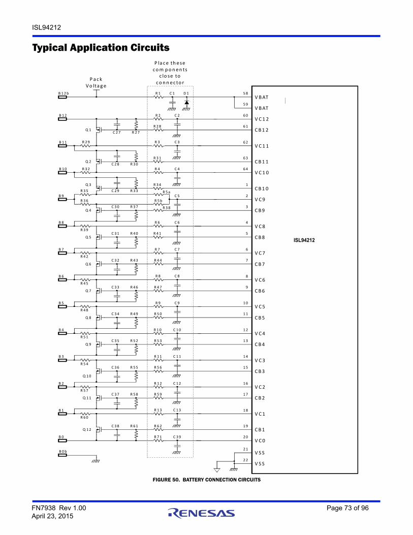
ISL94212
Typical Application Circuits
FIGURE 50. BATTERY CONNECTION CIRCUITS
R 29
Q 1C 27 R 27
R 2
R 28
C 2 60
61
V C1 2
CB1 2
B 12
R 32
Q 2C 28 R 30
R 3
R 31
C 3 62
63
V C1 1
CB1 1
B 11
R 35
Q 3
C 29 R 33
R 4
R 34
C 4 64
1
V C1 0
CB1 0
B 10
R 36
Q 4C 30 R 37
R 5a
R 38
C 5 2
3
V C9
CB9
B 9
R 39
Q 5C 31 R 40
R 6
R 41
C 6 4
5
V C8
CB8
B 8
R 42
Q 6C 32 R 43
R 7
R 44
C 7 6
7
V C7
CB7
B 7
R 45
Q 7C 33 R 46
R 8
R 47
C 8 8
9
V C6
CB6
B 6
R 48
Q 8C 34 R 49
R 9
R 50
C 9 10
11
V C5
CB5
B 5
R 51
Q 9C 35 R 52
R 10
R 53
C 10 12
13
V C4
CB4
B 4
R 54
Q 10
C 36 R 55
R 11
R 56
C 11 14
15
V C3
CB3
B 3
R 57
Q 11C 37 R 58
R 12
R 59
C 12 16
17
V C2
CB2
B 2
R 60
Q 12C 38 R 61
R 13
R 62
C 13 18
19
V C1
CB1
B 1
B 0 20V C0
D 1R 1 C 1 58
59
V BAT
V BAT
B 12b
21V S S
22V S S
B 0b
P la ce th ese com pon en ts
c lo se to co nn ec to r
IS L 9 4 2 1 2
R5b
C 39R 71
P a ck Vo lta g e
ISL94212
FN7938 Rev 1.00 Page 73 of 96April 23, 2015
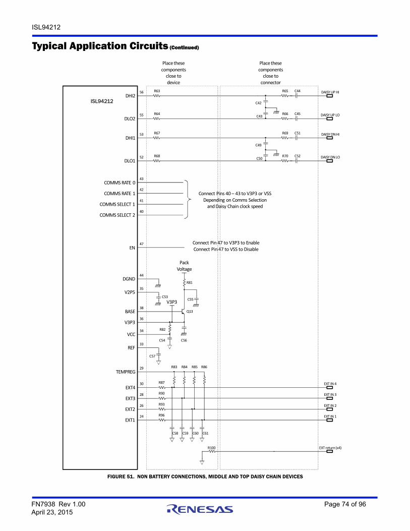
ISL94212
FIGURE 51. NON BATTERY CONNECTIONS, MIDDLE AND TOP DAISY CHAIN DEVICES
Typical Application Circuits (Continued)
C44
C45
R65
R66C43
C42
R63
R64
C51
C52
R69
R70C50
C49
R67
R68
DHI2
DLO2
56
55
53
52
DHI1
DLO1
COMMS RATE 0
COMMS RATE 1
COMMS SELECT 1
COMMS SELECT 2
43
42
41
40
DGND44
Connect Pin 47 to V3P3 to EnableConnect Pin 47 to VSS to Disable
V2P535
BASE38
V3P336
VCC34
REF33
EXT4
EXT3
EXT2
EXT1
C58 C59 C60 C61
30
28
26
24
DAISY UP HI
DAISY UP LO
DAISY DN HI
DAISY DN LO
EXT IN 4
EXT IN 3
EXT IN 2
EXT IN 1
R83 R84 R85 R86
TEMPREG29
Place these components close to connector
Place these components close to device
V3P3
R81
C53
C56
C55
C54
C57
R82
Q13
R87
R90
R93
R96
ISL94212
EN47
Pack Voltage
Connect Pins 40 – 43 to V3P3 or VSSDepending on Comms Selection and Daisy Chain clock speed
R100 EXT return (x4)
ISL94212
FN7938 Rev 1.00 Page 74 of 96April 23, 2015

ISL94212
FIGURE 52. NON BATTERY CONNECTIONS, MASTER DAISY CHAIN DEVICE
Typical Application Circuits (Continued)
DHI2
COMMS RATE 0
COMMS RATE 1
COMMS SELECT 1
COMMS SELECT 2
43
42
41
40
DGND44
Pack Voltage
V2P535
BASE38
V3P336
VCC34
REF33
EXT4
EXT3
EXT2
EXT1
C58 C59 C60 C61
30
28
26
24
EXT IN 4
EXT IN 3
EXT IN 2
EXT IN 1
R83 R84 R85 R86
TEMPREG29
Place these components close to connector
Place these components close to device
V3P3
R81
C53
C56
C55
C54
C57
R82
Q13
R87
R90
R93
R96
ISL94212
SCLK53
MicrocontrollerInterface
CS52
DIN50
DOUT49
DATA READY46
FAULT45
EN47
C44
C45
R65
R66C43
C42
R63
R64
DLO2
56
55
DAISY UP HI
DAISY UP LO
Connect Pins 40 –43 to V3P3 or VSSDepending on Comms Selection and Daisy Chain clock speed
Connect Pin 47 to V3P3 to EnableConnect Pin 47 to VSS to Disable
R100 EXT return (x4)
ISL94212
FN7938 Rev 1.00 Page 75 of 96April 23, 2015

ISL94212
FIGURE 53. BATTERY CONNECTION CIRCUITS ALTERNATIVE CONFIGURATION
Typical Application Circuits (Continued)
R29
Q1
C27 R27 R2
R28
C2 60
61
VC12
CB12
B12
R32
Q2
C28 R30 R3
R31
C3 62
63
VC11
CB11
B11
R35
Q3
C29 R33 R4
R34
C4 64
1
VC10
CB10
B10
R36
Q4C30 R37
R5
R38
C5 2
3
VC9
CB9
B9
R39
Q5C31 R40
R6
R41
C6 4
5
VC8
CB8
B8
R42
Q6C32 R43
R7
R44
C7 6
7
VC7
CB7
B7
R45
Q7C33 R46
R8
R47
C8 8
9
VC6
CB6
B6
R48
Q8C34 R49
R9
R50
C9 10
11
VC5
CB5
B5
R51
Q9C35 R52
R10
R53
C10 12
13
VC4
CB4
B4
R54
Q10C36 R55
R11
R56
C11 14
15
VC3
CB3
B3
R57
Q11C37 R58
R12
R59
C12 16
17
VC2
CB2
B2
R60
Q12C38 R61
R13
R62
C13 18
19
VC1
CB1
B1
B0 20VC0
D1R1 C1 58
59
VBAT
VBAT
B12b
21VSS
22VSS
B0b
Place these components close to connectorPack
Voltage
ISL94212
R71 C39
ISL94212
ISL94212
FN7938 Rev 1.00 Page 76 of 96April 23, 2015
ISL94212
Notes on Board Layout
Referring to Figure 50 on page 73 (battery connection circuits), the basic input filter structure comprises resistors R2 to R13, R71 and capacitors C2 to C13, C39. These components provide protection against transients and EMI for the cell inputs. They carry the loop currents produced by EMI and should be placed as close to the connector as possible. The ground terminals of the capacitors must be connected directly to a solid ground plane. Do not use vias to connect these capacitors to the input signal path or to ground. Any vias should be placed in line to the signal inputs so that the inductance of these forms a low pass filter with the grounded capacitors.
Referring to Figure 51 on page 74, the daisy chain components are shown to the top right of the drawing. These are split into two sections. Components to the right of this section should be placed close to the board connector with the ground terminals of capacitors connected directly to a solid ground plane. This is the same ground plane that serves the cell inputs. Components to the left of this section should be placed as closely to the device as possible.
The battery connector and daisy chain connectors should be placed closely to each other on the same edge of the board to minimize any loop current area.
Two grounds are identified on the circuit diagram. These are nominally referred to as noisy and quiet grounds. The noisy ground, denoted by an “earth” symbol carries the EMI loop currents and digital ground currents while the quiet ground is used to define the decoupling voltage for voltage reference and the analog power supply rail. The quiet and noisy grounds should be joined at the VSS pin. Keep the quiet ground area as small as possible.
The circuits shown to the bottom right of Figure 51 on page 74 provide signal conditioning and EMI protection for the external temperature inputs. These inputs are designed to operate with external NTC thermistors. See “External Inputs” on page 85 for more information about component selection.
TABLE 48. RECOMMENDED COMPONENT VALUES FOR FIGURES (Figures 50 to 53)
RESISTORS
VALUE COMPONENTS
0 R101
27 R1
33 R82
1k R2, R3, R4, R5, R6, R7, R8, R9, R10, R11, R12, R13, R71
100 R29, R32, R35, R36, R39, R42, R45, R48, R51, R54, R57, R60, R63, R64, R67, R68, R81
2k R5a, R5b
470 R65, R66, R69, R70
10k R28, R31, R34, R38, R41, R44, R47, R50, R53, R56, R59, R62, R83, R84, R85, R86, R87, R90, R93, R96, R100a, R100b, R100c, R100d
330k R27, R30, R33, R37, R40, R43, R46, R49, R52, R55, R58, R61
CAPACITORS
VALUE VOLTAGE COMPONENTS
200p 100 C42, C43, C49, C50
220p 500 C44, C45, C51, C52
10n 50 C27, C28, C29, C30, C31, C32, C33, C34, C35, C36, C37, C38, C58, C59, C60, C61
22n 100 C2, C3, C4, C5, C6, C7, C8, C9, C10, C11, C12, C13, C39
220n 100 C1
1µ 10 C53, C54, C56
1µ 100 C55
2.2µ 10 C57
ZENER DIODES
VALUE EXAMPLE COMPONENTS
60V 1N5371BRLG D1
FN7938 Rev 1.00 Page 77 of 96April 23, 2015
ISL94212
Component Selection Certain failures associated with external components can lead to unsafe conditions in electronic modules. A good example of this is a component that is connected between high energy signal sources failing short. Such a condition can easily lead to the component overheating and damaging the board and other components in its proximity.
One area to consider with the external circuits on the ISL94212 is the capacitors connected to the cell monitoring inputs. These capacitors are normally protected by the series protection resistors but could present a safety hazard in the event of a dual point fault where both the capacitor and associated series resistor fail short. Also, a short in one of these capacitors would dissipate the charge in the battery cell if left uncorrected for an extended period of time. It is recommended that capacitors C1 to C13 be selected to be “fail safe” or “open mode” types. An alternative strategy would be to replace each of these capacitors with two devices in series, each with double the value of the single capacitor.
A dual point failure in the balancing resistor (R29, R32, R35, etc.) of Figure 50 on page 73 and associated balancing MOSFET (Q1 to Q12) could also give rise to a shorted cell condition. It is recommended that the balancing resistor be replaced by two resistors in series.
Operating the ISL94212 with Reduced Cell CountsWhen using the ISL94212 with fewer than 12 cells it is important to ensure that each used cell has a normal input circuit connection to the top and bottom monitoring inputs for that cell. The simplest way to use the ISL94212 with any number of cells is to always use the full input circuit arrangement for all inputs, and short together the unused inputs at the battery terminal. In this way each cell input sees a normal source impedance independent of whether or not it is monitoring a cell.
The cell balancing components associated with unconnected cell inputs are not required and can be removed. Unused cell balance outputs should be tied to the adjacent cell voltage monitoring pin.
The input circuit component count can be reduced in cases where fewer than 10 cells are being monitored. It is important that cell inputs that are being used are not connected to other (unused) cell inputs as this would affect measurement accuracy. Figure 54 on page 79, Figure 55 on page 80, and Figure 56 on page 81 show examples of systems with 10 cells, 8 cells, and 6 cells, respectively.
The component notations and values used in Figures 55 and 56 are the same as those used in Figures 50 to 53.
In Figure 56 the resistor associated with the input filter on VC9 is noted as R5, rather than R5a. This value change is needed to maintain the correct input network impedance in the absence of the cell 9 balance circuits.
FN7938 Rev 1.00 Page 78 of 96April 23, 2015
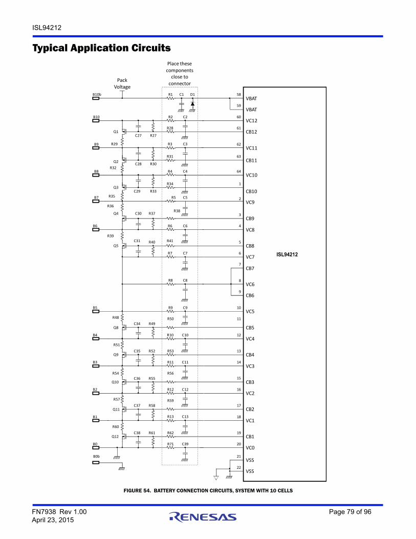
ISL94212
Typical Application Circuits
FIGURE 54. BATTERY CONNECTION CIRCUITS, SYSTEM WITH 10 CELLS
R29
Q1C27 R27
R2
R28
C2 60
61
VC12
CB12
B10
R32
Q2C28 R30
R3
R31
C3 62
63
VC11
CB11
B9
R35
Q3C29 R33
R4
R34
C4 64
1
VC10
CB10
B8
R36
Q4 C30 R37R38
C5 2
3
VC9
CB9
B7
R39
Q5C31 R40
R6
R41
C6 4
5
VC8
CB8
B6
R7 C7 6
7
VC7
CB7
R8 C8 8
9
VC6
CB6
R48
Q8C34 R49
R9
R50
C9 10
11
VC5
CB5
B5
R51
Q9C35 R52
R10
R53
C10 12
13
VC4
CB4
B4
R54
Q10C36 R55
R11
R56
C11 14
15
VC3
CB3
B3
R57
Q11C37 R58
R12
R59
C12 16
17
VC2
CB2
B2
R60
Q12C38 R61
R13
R62
C13 18
19
VC1
CB1
B1
B0 20VC0
D1R1 C1 58
59
VBAT
VBAT
B10b
21VSS
22VSS
B0b
Place these components close to connector
ISL94212
R5
R71 C39
Pack Voltage
ISL94212
FN7938 Rev 1.00 Page 79 of 96April 23, 2015
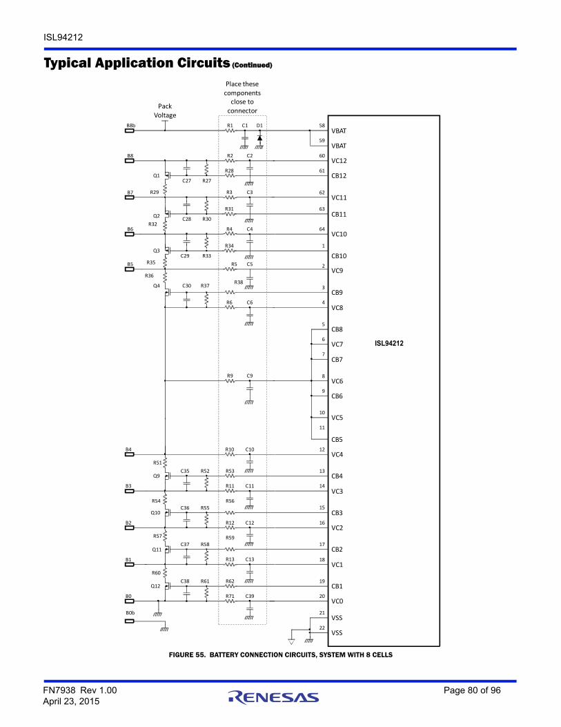
ISL94212
FIGURE 55. BATTERY CONNECTION CIRCUITS, SYSTEM WITH 8 CELLS
Typical Application Circuits (Continued)
R29
Q1C27 R27
R2
R28
C2 60
61
VC12
CB12
B8
R32
Q2C28 R30
R3
R31
C3 62
63
VC11
CB11
B7
R35
Q3C29 R33
R4
R34
C4 64
1
VC10
CB10
B6
R36
Q4 C30 R37R38
C5 2
3
VC9
CB9
B5
R6 C6 4
5
VC8
CB8
6
7
VC7
CB7
R9 C9 8
9
VC6
CB6
10
11
VC5
CB5
R51
Q9C35 R52
R10
R53
C10 12
13
VC4
CB4
B4
R54
Q10C36 R55
R11
R56
C11 14
15
VC3
CB3
B3
R57
Q11C37 R58
R12
R59
C12 16
17
VC2
CB2
B2
R60
Q12C38 R61
R13
R62
C13 18
19
VC1
CB1
B1
B0 20VC0
D1R1 C1 58
59
VBAT
VBAT
B8b
21VSS
22VSS
B0b
Place these components close to connector
ISL94212
R5
R71 C39
Pack Voltage
ISL94212
FN7938 Rev 1.00 Page 80 of 96April 23, 2015
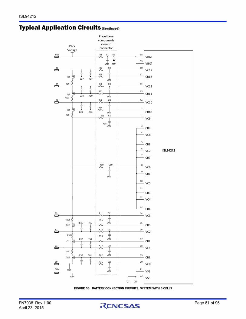
ISL94212
FIGURE 56. BATTERY CONNECTION CIRCUITS, SYSTEM WITH 6 CELLS
Typical Application Circuits (Continued)
R29
Q1C27 R27
R2
R28
C2 60
61
VC12
CB12
B6
R32
Q2C28 R30
R3
R31
C3 62
63
VC11
CB11
B5
R35
Q3C29 R33
R4
R34
C4 64
1
VC10
CB10
B4
R38
C5 2
3
VC9
CB9
4
5
VC8
CB8
6
7
VC7
CB7
R10 C10 8
9
VC6
CB6
10
11
VC5
CB5
12
13
VC4
CB4
R54
Q10C36 R55
R11
R56
C11 14
15
VC3
CB3
B3
R57
Q11C37 R58
R12
R59
C12 16
17
VC2
CB2
B2
R60
Q12C38 R61
R13
R62
C13 18
19
VC1
CB1
B1
B0 20VC0
D1R1 C1 58
59
VBAT
VBAT
B6b
21VSS
22VSS
B0b
Place these components close to connector
ISL94212
R5
R71 C39
Pack Voltage
ISL94212
FN7938 Rev 1.00 Page 81 of 96April 23, 2015
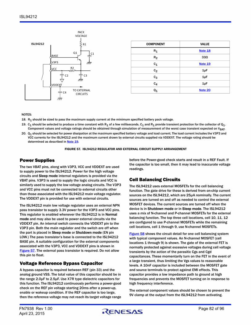
ISL94212
Power SuppliesThe two VBAT pins, along with V3P3, VCC and VDDEXT are used to supply power to the ISL94212. Power for the high voltage circuits and Sleep mode internal regulators is provided via the VBAT pins. V3P3 is used to supply the logic circuits and VCC is similarly used to supply the low voltage analog circuits. The V3P3 and VCC pins must not be connected to external circuits other than those associated with the ISL94212 main voltage regulator. The VDDEXT pin is provided for use with external circuits.
The ISL94212 main low voltage regulator uses an external NPN pass transistor to supply 3.3V power for the V3P3 and VCC pins. This regulator is enabled whenever the ISL94212 is in Normal mode and may also be used to power external circuits via the VDDEXT pin. An internal switch connects the VDDEXT pin to the V3P3 pin. Both the main regulator and the switch are off when the part is placed in Sleep mode or Shutdown mode (EN pin LOW.) The pass transistor’s base is connected to the ISL94212 BASE pin. A suitable configuration for the external components associated with the V3P3, VCC and VDDEXT pins is shown in Figure 57. The external pass transistor is required. Do not allow this pin to float.
Voltage Reference Bypass CapacitorA bypass capacitor is required between REF (pin 33) and the analog ground VSS. The total value of this capacitor should be in the range 2.0µF to 2.5µF. Use X7R type dielectric capacitors for this function. The ISL94212 continuously performs a power-good check on the REF pin voltage starting 20ms after a power-up, enable or wakeup condition. If the REF capacitor is too large, then the reference voltage may not reach its target voltage range
before the Power-good check starts and result in a REF Fault. If the capacitor is too small, then it may lead to inaccurate voltage readings.
Cell Balancing CircuitsThe ISL94212 uses external MOSFETs for the cell balancing function. The gate drive for these is derived from on-chip current sources on the ISL94212, which are 25µA nominally. The current sources are turned on and off as needed to control the external MOSFET devices. The current sources are turned off when the device is in Shutdown mode or in Sleep mode. The ISL94212 uses a mix of N-channel and P-channel MOSFETs for the external balancing function. The top three cell locations, cell 10, 11, 12 are configured to use P-channel MOSFETs while the remaining cell locations, cell 1 through 9, use N-channel MOSFETs.
Figure 58 shows the circuit detail for one cell balancing system with typical component values. An N-channel MOSFET (cell locations 1 through 9) is shown. The gate of the external FET is normally protected against excessive voltages during cell voltage transients by the action of the parasitic Cgs and Cgd capacitances. These momentarily turn on the FET in the event of a large transient, thus limiting the Vgs values to reasonable levels. A 10nF capacitor is included between the MOSFET gate and source terminals to protect against EMI effects. This capacitor provides a low impedance path to ground at high frequencies and prevents the MOSFET turning on in response to high frequency interference.
The external component values should be chosen to prevent the 9V clamp at the output from the ISL94212 from activating.
FIGURE 57. ISL94212 REGULATOR AND EXTERNAL CIRCUIT SUPPLY ARRANGEMENT
TO EXTERNAL CIRCUITS
R1
VDDEXT
C3
ISL78600ISL78610
VCC
V3P3
BASE
C2
C4
C1
R2
Q1
PACKVOLTAGE
D1
ISL94212 COMPONENT VALUE
R1 Note 18
R2 33Ω
C1 Note 19
C2 1μF
C3 1μF
C4 1μF
Q1 Note 20
NOTES:
18. R1 should be sized to pass the maximum supply current at the minimum specified battery pack voltage.
19. C1 should be selected to produce a time constant with R1 of a few milliseconds. C1 and R1 provide transient protection for the collector of Q1. Component values and voltage ratings should be obtained through simulation of measurement of the worst case transient expected on VBAT.
20. Q1 should be selected for power dissipation at the maximum specified battery voltage and load current. The load current includes the V3P3 and VCC currents for the ISL94212 and the maximum current drawn by external circuits supplied via VDDEXT. The voltage rating should be determined as described in Note 19.
FN7938 Rev 1.00 Page 82 of 96April 23, 2015
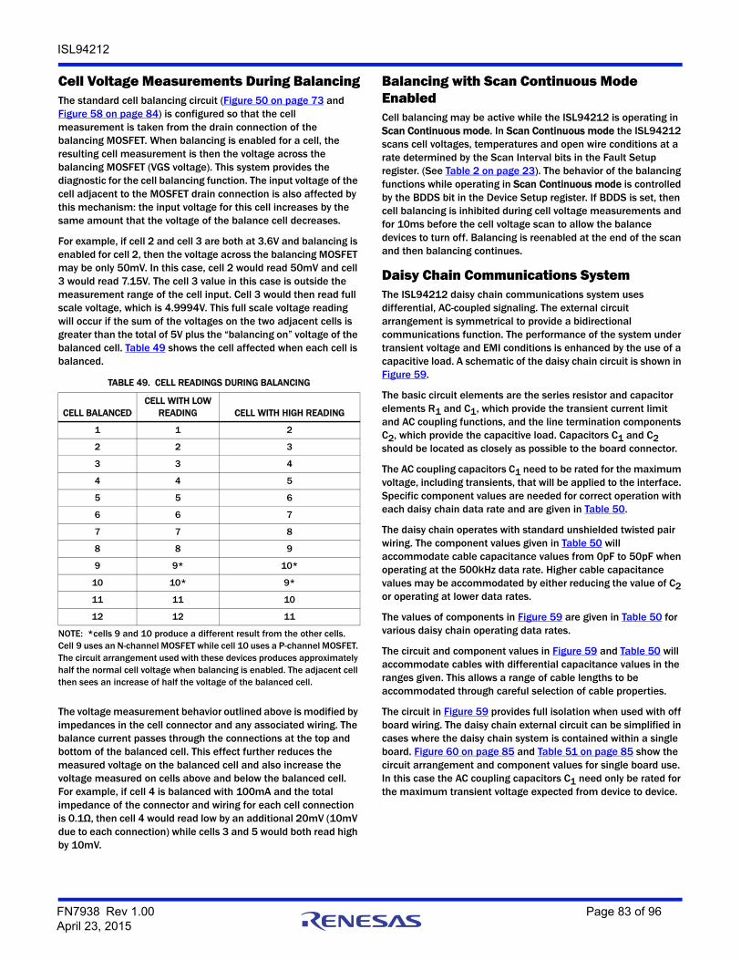
ISL94212
Cell Voltage Measurements During BalancingThe standard cell balancing circuit (Figure 50 on page 73 and Figure 58 on page 84) is configured so that the cell measurement is taken from the drain connection of the balancing MOSFET. When balancing is enabled for a cell, the resulting cell measurement is then the voltage across the balancing MOSFET (VGS voltage). This system provides the diagnostic for the cell balancing function. The input voltage of the cell adjacent to the MOSFET drain connection is also affected by this mechanism: the input voltage for this cell increases by the same amount that the voltage of the balance cell decreases.
For example, if cell 2 and cell 3 are both at 3.6V and balancing is enabled for cell 2, then the voltage across the balancing MOSFET may be only 50mV. In this case, cell 2 would read 50mV and cell 3 would read 7.15V. The cell 3 value in this case is outside the measurement range of the cell input. Cell 3 would then read full scale voltage, which is 4.9994V. This full scale voltage reading will occur if the sum of the voltages on the two adjacent cells is greater than the total of 5V plus the “balancing on” voltage of the balanced cell. Table 49 shows the cell affected when each cell is balanced.
The voltage measurement behavior outlined above is modified by impedances in the cell connector and any associated wiring. The balance current passes through the connections at the top and bottom of the balanced cell. This effect further reduces the measured voltage on the balanced cell and also increase the voltage measured on cells above and below the balanced cell. For example, if cell 4 is balanced with 100mA and the total impedance of the connector and wiring for each cell connection is 0.1Ω, then cell 4 would read low by an additional 20mV (10mV due to each connection) while cells 3 and 5 would both read high by 10mV.
Balancing with Scan Continuous Mode EnabledCell balancing may be active while the ISL94212 is operating in Scan Continuous mode. In Scan Continuous mode the ISL94212 scans cell voltages, temperatures and open wire conditions at a rate determined by the Scan Interval bits in the Fault Setup register. (See Table 2 on page 23). The behavior of the balancing functions while operating in Scan Continuous mode is controlled by the BDDS bit in the Device Setup register. If BDDS is set, then cell balancing is inhibited during cell voltage measurements and for 10ms before the cell voltage scan to allow the balance devices to turn off. Balancing is reenabled at the end of the scan and then balancing continues.
Daisy Chain Communications SystemThe ISL94212 daisy chain communications system uses differential, AC-coupled signaling. The external circuit arrangement is symmetrical to provide a bidirectional communications function. The performance of the system under transient voltage and EMI conditions is enhanced by the use of a capacitive load. A schematic of the daisy chain circuit is shown in Figure 59.
The basic circuit elements are the series resistor and capacitor elements R1 and C1, which provide the transient current limit and AC coupling functions, and the line termination components C2, which provide the capacitive load. Capacitors C1 and C2 should be located as closely as possible to the board connector.
The AC coupling capacitors C1 need to be rated for the maximum voltage, including transients, that will be applied to the interface. Specific component values are needed for correct operation with each daisy chain data rate and are given in Table 50.
The daisy chain operates with standard unshielded twisted pair wiring. The component values given in Table 50 will accommodate cable capacitance values from 0pF to 50pF when operating at the 500kHz data rate. Higher cable capacitance values may be accommodated by either reducing the value of C2 or operating at lower data rates.
The values of components in Figure 59 are given in Table 50 for various daisy chain operating data rates.
The circuit and component values in Figure 59 and Table 50 will accommodate cables with differential capacitance values in the ranges given. This allows a range of cable lengths to be accommodated through careful selection of cable properties.
The circuit in Figure 59 provides full isolation when used with off board wiring. The daisy chain external circuit can be simplified in cases where the daisy chain system is contained within a single board. Figure 60 on page 85 and Table 51 on page 85 show the circuit arrangement and component values for single board use. In this case the AC coupling capacitors C1 need only be rated for the maximum transient voltage expected from device to device.
TABLE 49. CELL READINGS DURING BALANCING
CELL BALANCEDCELL WITH LOW
READING CELL WITH HIGH READING
1 1 2
2 2 3
3 3 4
4 4 5
5 5 6
6 6 7
7 7 8
8 8 9
9 9* 10*
10 10* 9*
11 11 10
12 12 11
NOTE: *cells 9 and 10 produce a different result from the other cells. Cell 9 uses an N-channel MOSFET while cell 10 uses a P-channel MOSFET. The circuit arrangement used with these devices produces approximately half the normal cell voltage when balancing is enabled. The adjacent cell then sees an increase of half the voltage of the balanced cell.
FN7938 Rev 1.00 Page 83 of 96April 23, 2015
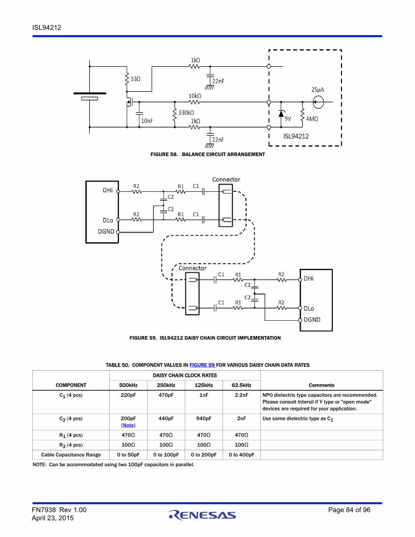
ISL94212
FIGURE 58. BALANCE CIRCUIT ARRANGEMENT
ISL94212
FIGURE 59. ISL94212 DAISY CHAIN CIRCUIT IMPLEMENTATION
TABLE 50. COMPONENT VALUES IN FIGURE 59 FOR VARIOUS DAISY CHAIN DATA RATES
COMPONENT
DAISY CHAIN CLOCK RATES
Comments500kHz 250kHz 125kHz 62.5kHz
C1 (4 pcs) 220pF 470pF 1nF 2.2nF NPO dielectric type capacitors are recommended. Please consult Intersil if Y type or "open mode" devices are required for your application.
C2 (4 pcs) 200pF(Note)
440pF 940pF 2nF Use same dielectric type as C1
R1 (4 pcs) 470Ω 470Ω 470Ω 470Ω
R2 (4 pcs) 100Ω 100Ω 100Ω 100Ω
Cable Capacitance Range 0 to 50pF 0 to 100pF 0 to 200pF 0 to 400pF
NOTE: Can be accommodated using two 100pF capacitors in parallel.
FN7938 Rev 1.00 Page 84 of 96April 23, 2015

ISL94212
.
External InputsThe ISL94212 provides 4 external inputs for use either as general purpose analog inputs or for NTC type thermistors. Each of the external inputs has an internal pull-up resistor, which is connected by a switch to the VCC pin whenever the TEMPREG output is active. This arrangement results in an open input being pulled up to the VCC voltage.
Inputs above 15/16 of full scale are registered as open inputs and cause the relevant bit in the Over-temperature Fault register, along with the OT bit in the Fault Status register to be set, on condition of the respective temperature test enable bit in the Fault Setup register. The user must then read the register value associated with the faulty input to determine if the fault was due to an open input (value above 15/16 full scale) or an over-temperature condition (value below the external temp limit setting).
The arrangement of the external inputs is shown in Figure 61 using the ExT4 input as an example. It is important that the components are connected in the sequence shown in Figure 61, e.g., C1 must be connected such the trace from this capacitor’s positive terminal connects to R2 before connecting to R1. This guarantees the correct operation of the various fault detection functions.
The function of each of the components in Figure 61 is listed in Table 52 together with the diagnostic result of an open or short fault in each component
FIGURE 60. ISL94212 DAISY CHAIN – BOARD LEVEL IMPLEMENTATION CIRCUIT
TABLE 51. DAISY CHAIN COMPONENT VALUES FOR BOARD LEVEL IMPLEMENTATION
COMPONENT TOLERANCE
DAISY CHAIN DATA RATE
500kHz 250kHz 125kHz 62.5kHz
C1 (2 pcs) 5% 100pF 220pF 470pF 1nF
C2 (4 pcs) 5% 220pF 470pF 1nF 2.2nF
R1 (4 pcs) 1kΩ 1kΩ 1kΩ 1kΩ
FIGURE 61. CONNECTION OF NTC THERMISTOR TO INPUT EXT4
ISL94212
FN7938 Rev 1.00 Page 85 of 96April 23, 2015

ISL94212
Board Level CalibrationFor best accuracy, the ISL94212 may be recalibrated after soldering to a board using a simple resistor trim. The adjustment method involves obtaining the average cell reading error for the cell inputs at a single temperature and cell voltage value and applying a select-on-test resistor to zero the average cell reading error.
The adjustment system uses a resistor placed either between VDDEXT and VREF or VREF and VSS as shown in Figure 62. The value of resistor R1 or R2 is then selected based on the average error measured on all cells at 3.3V per cell and room temperature e.g., with 3.3V on each cell input scan the voltage values using the ISL94212 and record the average reading error (ISL94212 reading – cell voltage value). Table 53 shows the value of R1 and R2 required for various measured errors.
To use Table 53, find the measured error value closest to the result obtained with measurements using the ISL94212 and select the corresponding resistor value. Alternatively, if finer adjustment resolution is required then this may be obtained by interpolation using Table 53. Worked Examples
The following worked examples are provided to assist with the setup and calculations associated with various functions.
Voltage Reference Check Calculation
TABLE 52. COMPONENT FUNCTIONS AND DIAGNOSTIC RESULTS FOR CIRCUIT OF FIGURE 61
COMPONENT FUNCTION DIAGNOSTIC RESULT
R1 Protection from wiring shorts to external HV connections.
Open: Open wire detectionShort: No diagnostic result
R2 Measurement high-side resistor Open: Low input level (over-temperature indication)Short: High input level (open wire indication).
Thermistor Open: High input level (open wire indication).Short: Low input level (over-temperature indication)
C1 Noise Filter. Connects to measurement ground VSS.
Open: no diagnostic result.Short: Low input level (over-temperature indication)
FIGURE 62. CELL READING ACCURACY ADJUSTMENT SYSTEM
TABLE 53. COMPONENT VALUES FOR ACCURACY CALIBRATION ADJUSTMENT OF FIGURE 62
MEASURED ERROR AT VC = 3.3V (mV)
V78600 - VCELL (mV)R1
(kΩ)R2
(kΩ)
4 205 DNP
3 274 DNP
2 412 DNP
1 825 DNP
0 DNP DNP
-1 DNP 2550
-2 DNP 1270
-3 DNP 866
-4 DNP 649
DNP = Do Not populate
TABLE 54. EXAMPLE REGISTER DATA
R/W PAGE ADDRESS PARAMETERVALUE(HEX) DECIMAL
0 001 010000 IC Temperature 14’h2425 9253
0 001 010101 Reference Voltage 14’h20A7 8359
0 010 111000 Coefficient C 14’h00A4 164
0 010 111001 Coefficient B 14’h3FCD -51
0 010 111010 Coefficient A 9’h006 6
FN7938 Rev 1.00 Page 86 of 96April 23, 2015
ISL94212
Coefficients A, B and C are two’s compliment numbers. B and C have a range +8191 to -8192. A has a range +255 to -256.
Coefficient B above is a negative number (Hex value > 1FFF). The value for B is 14’h3FCD - 14h3FFF- 1 or (1633310 -1638310 - 1) = -51.
Coefficient A occupies the upper 9 bits of register 6’b111010 (6'h3A). One way to extract the coefficient data from this register is to divide the complete register value by 32 and rounding the result down to the nearest integer. With 9'h006 in the upper 9 bits, and assuming the lower 5 bits are 0, the complete register value will be 14'h0C0 = 192 decimal. Divide this by 32 to obtain 6.
Coefficients A, B and C are used with the IC temperature reading to calibrate the Reference Voltage reading. The calibration is applied by subtracting an adjustment of the form (see Equation 5) from the Reference Voltage reading.
An example calculation using the data from Table 54 is given in Equation 6.
Where 9180 is the Internal Temperature Monitor reading at +25°C (see the “Electrical Specifications” table, TINT25 on page 10).
Cell Balancing – Manual ModeRefer to “Manual Balance Mode” on page 26.
EXAMPLE: ACTIVATE BALANCING ON CELLS 1, 5, 7 AND 11Step 1. Write Balance Setup register: Set Manual Balance mode, Balance Status pointer, and turn off balance.
BMD = 01 (Manual Balance mode)BWT = XXXBSP = 0000 (Balance status pointer location 0)BEN = 0 (Balancing disabled)
Note: Green text indicates a register change.
Step 2. Write Balance Status register: Set bits 0, 4, 6 and 10
BAL12:1 = 0100 0101 0001
Step 3. Enable balancing using Balance Enable command
Or enable balancing by setting BEN directly in the Balance Setup register:
BEN = 1
The balance FETs attached to cells 1, 5, 7 and 11 turn on.
Turn balancing off by resetting BEN or by sending the Balance Inhibit command (Page 3, address 6’h11).
Cell Balancing – Timed ModeRefer to “Timed Balance Mode” on page 27.
EXAMPLE: ACTIVATE BALANCING ON CELLS 2 AND 8 FOR 1 MINUTE.Step 1. Write Balance Setup register: Set Timed Balance mode, Balance Status pointer, and turn off balance.
BMD = 10 (Timed Balance mode)BWT = XXXBSP = 0000 (Balance status pointer location 0)BEN = 0 (BALANCING disabled)
Step 2. Write Balance Status register: Set bits 1 and 7
BAL12:1 = 0000 1000 0010BALANCE SETUP REGISTER
R/W PAGE ADDRESS DATA
1 010 010011 XX XX00 000X XX01
X = don’t care
(EQ. 5)AdjustmentA
256 8192----------------------------- dT
2 B8192-------------+ dT C+=
(EQ. 6)dT9253 9180–
2-------------------------------- 36.5= =
(EQ. 7)Adjustment
6256 8192----------------------------- 36.5 2 51
8192------------- 36.5 164 163.8=+–=
(EQ. 8)Corrected VREF 8359 163.8 8195.2=–=
(EQ. 9)VREF value8195.216384------------------ 5 2.5010==
BALANCE STATUS REGISTER
R/W PAGE ADDRESS DATA
1 010 010100 XX 0100 0101 0001
BALANCE ENABLE COMMAND
R/W PAGE ADDRESS DATA
0 011 010000 00 0000
BALANCE SETUP REGISTER
R/W PAGE ADDRESS DATA
1 010 010011 XX XX1X XXXX XXXX
BALANCE SETUP REGISTER
R/W PAGE ADDRESS DATA
1 010 010011 XX XX00 000X XX10
X = don’t care
BALANCE STATUS REGISTER
R/W PAGE ADDRESS DATA
1 010 010100 XX 0000 1000 0010
FN7938 Rev 1.00 Page 87 of 96April 23, 2015
ISL94212
Step 3. Write balance timeout setting to the Watchdog/Balance Time register (page 2, address 6’h15, bits [13:7])
BTM6:1 = 0000011 (1 minute)
Step 4. Enable balancing using Balance Enable command
Or enable balancing by setting BEN directly in the Balance Setup register:
BEN = 1
The balance FETs attached to cells 2 and 8 turn on. The FETs turn off after 1 minute. Balancing may be stopped by resetting BEN or by sending the Balance Inhibit command.
Cell Balancing – Auto ModeRefer to “Auto Balance Mode” on page 27.
BALANCE VALUE CALCULATION EXAMPLEThis example is based on a cell State of Charge (SOC) of 9360 coulombs, a target SOC of 8890 coulombs, a balancing leg impedance of 31Ω (30Ω resistor plus 1Ω FET on resistance) and a sampling time interval of 5 minutes (300 seconds).
The Balance Value is calculated using Equation 10.
The value 8191/5 is the scaling factor of the cell voltage measurement.
The value of 28’h00136CA is loaded to the required Cell Balance Register and the value 7’b0001111 (5 minutes) is loaded to the Balance Time bits in the Watchdog/Balance time register.
In this example, the total coulomb difference to be balanced is: 470 coulomb (9360 - 8890). At 3.3V/31Ω*300s = 31.9 coulomb per cycle, it takes about 15 cycles for the balancing to terminate.
AUTO BALANCE MODE CELL BALANCING EXAMPLEThe following describes a simple setup to demonstrate the Auto Balance mode cell balancing function of the ISL94212. Note that this balancing setup is not related to the balance value calculation in Equation 10.
Auto balance cells using the following criteria:
• Balance time = 20s
• Balance wait time (dead time between balancing cycles) = 8s
• Balancing disabled during cell measurements.
• Balance Values: See Table 55
• Balance Status Register: Set up balance:Cells 1, 4, 7 and 10 on 1st cycle. Cells 3, 6, 9 and 12 on 2nd cycle. Cells 2, 5, 8 and 11 on 3rd cycle(See Table 56)
WATCHDOG/BALANCE TIME REGISTER
R/W PAGE ADDRESS DATA
1 010 010101 00 0001 1XXX XXXX
X = don’t care – the lower bits are the watchdog timeout value and should be set to a time longer than the balance time. A value of 111 1111 is suggested.
BALANCE ENABLE COMMAND
R/W PAGE ADDRESS DATA
0 011 010000 00 0000
BALANCE SETUP REGISTER
R/W PAGE ADDRESS DATA
1 010 010011 XX XX1X XXXX XXXX
B8191
5------------- 9360 8890– 31
300---------- 79562= 28 h00136CA== (EQ. 10)
TABLE 55. CELL BALANCE VALUES (HEX) FOR EACH CELL
CELL 1
CELL 2
CELL 3
CELL 4
CELL 5
CELL 6
CELL 7
CELL 8
CELL 9
CELL 10
CELL 11
CELL 12
28’h406A
28’h3E4D
28’h0
28’h292F
28’h3E00
28’h0
28’h2903
28’h3D06
28’h0
28’h151E
28’h502
28’h6D6
TABLE 56. BALANCE STATUS SETUP
BPS[3:0]
CELL
1 2 3 4 5 6 7 8 9 10 11 12
0000 Reserved for Manual Balance mode and Timed Balance mode
0001 1 0 0 1 0 0 1 0 0 1 0 0
0010 0 0 1 0 0 1 0 0 1 0 0 1
0011 0 1 0 0 1 0 0 1 0 0 1 0
FN7938 Rev 1.00 Page 88 of 96April 23, 2015

ISL94212
Step 1. Write Balance Value registers
Step 2. Write BDDS bit in Device Setup register (turn balancing functions off during measurement)
BDDS = 1
Step 3. Write balance timeout setting to the Watchdog/Balance Time register: Balance timeout code = 0000001 (20 seconds)
BTM6:0 = 000 0001
Step 4. Set up Balance Status register (from Table 56 on page 88)
Step 4A. Write Balance Setup register: Set Auto Balance mode, set 8 second Balance wait time, and set balance off:
BMD = 11 (Auto Balance mode)BWT = 100 (8 seconds)BEN = 0 (Balancing disabled)
Step 4B. Write Balance Setup register: Set Balance Status Pointer = 1
BSP = 0001 (Balance status pointer = 1)
Step 4C. Write Balance Status register: Set bits 1, 4, 7 and 10
BAL12:1 = 0010 0100 1001
Step 4D. Write Balance Setup register: Set Balance Status Pointer = 2
BSP = 0010 (Balance status pointer = 2)
BALANCE VALUE REGISTERS
R/W PAGE ADDRESS DATA (HEX) CELL
1 010 100000 14’h006A 1
1 010 100001 14’h0001
1 010 100010 14’h3E4D 2
1 010 100011 14’h0000
1 010 100100 14’h0000 3
1 010 100101 14’h0000
1 010 100110 14’h292F 4
1 010 100111 14’h0000
1 010 101000 14’h3E00 5
1 010 101001 14’h0000
1 010 101010 14’h0000 6
1 010 101011 14’h0000
1 010 101100 14’h2903 7
1 010 101101 14’h0000
1 010 101110 14’h3D06 8
1 010 101111 14’h0000
1 010 110000 14’h0000 9
1 010 110001 14’h0000
1 010 110010 14’h151E 10
1 010 110011 14’h0000
1 010 110100 14’h0502 11
1 010 110101 14’h0000
1 010 110110 14’h06D6 12
1 010 110111 14’h0000
BALANCE VALUE REGISTERS (CELL1) - VALUE 28’h406A
6’20 B0107 B0106 B0105 B0104 B0103 B0102 B0101 B0100
0 1 1 0 1 0 1 0
B0113 B0112 B1011 B0110 B0109 B0108
0 0 0 0 0 0
6’21 B0121 B0120 B0119 B0118 B0117 B0116 B0115 B0114
0 0 0 0 0 0 0 1
B0127 B0126 B0125 B0124 B0123 B0122
0 0 0 0 0 0
DEVICE SETUP REGISTER
R/W PAGE ADDRESS DATA
1 010 011001 XX XXXX 1XXX XXXX
X = don’t care
BALANCE TIMEOUT REGISTER
R/W PAGE ADDRESS DATA
1 010 010101 00 0000 1XXX XXXX
X = don’t care – the lower bits are the watchdog timeout value and should be set to a time longer than the balance time. A value 111 1111 is suggested.
BALANCE SETUP REGISTER
R/W PAGE ADDRESS DATA
1 010 010011 XX XX0X XXX1 0011
X = don’t care
BALANCE SETUP REGISTER
R/W PAGE ADDRESS DATA
1 010 010011 XX XXX0 001X XXXX
X = don’t care
BALANCE STATUS REGISTER
R/W PAGE ADDRESS DATA
1 010 010100 XX 0010 0100 1001
BALANCE SETUP REGISTER
R/W PAGE ADDRESS DATA
1 010 010011 XX XXX0 010X XXXX
X = don’t care
FN7938 Rev 1.00 Page 89 of 96April 23, 2015
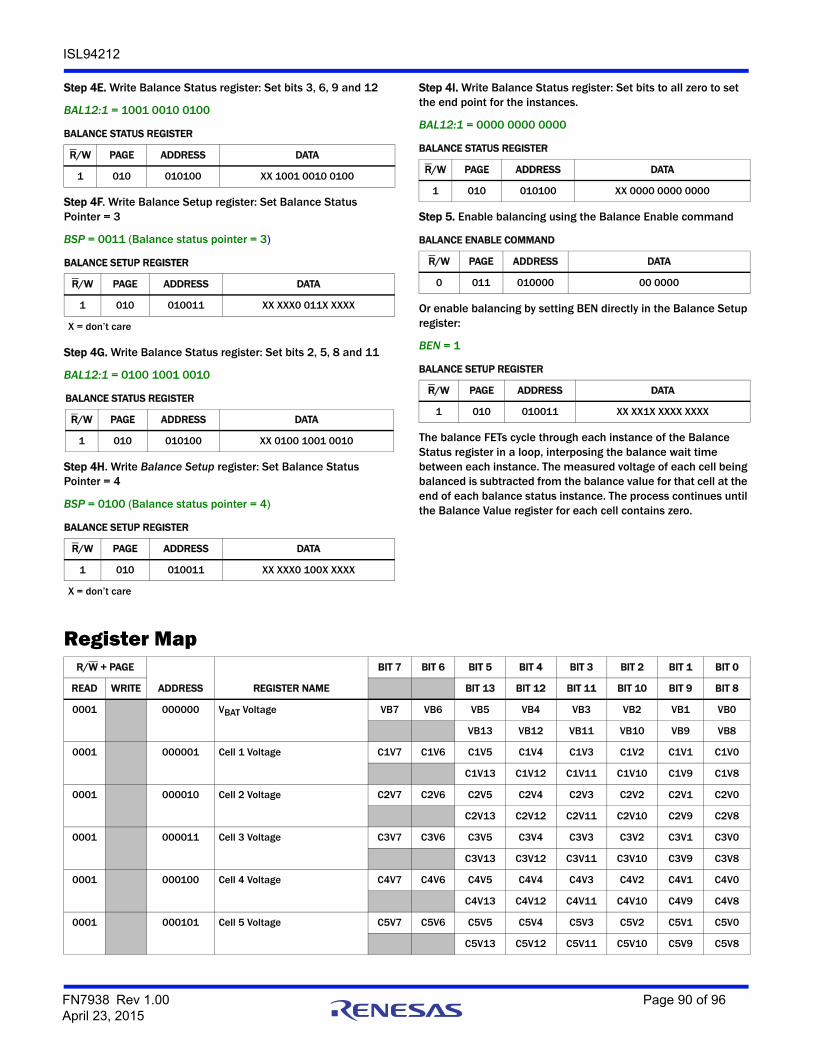
ISL94212
Step 4E. Write Balance Status register: Set bits 3, 6, 9 and 12
BAL12:1 = 1001 0010 0100
Step 4F. Write Balance Setup register: Set Balance Status Pointer = 3
BSP = 0011 (Balance status pointer = 3)
Step 4G. Write Balance Status register: Set bits 2, 5, 8 and 11
BAL12:1 = 0100 1001 0010
Step 4H. Write Balance Setup register: Set Balance Status Pointer = 4
BSP = 0100 (Balance status pointer = 4)
Step 4I. Write Balance Status register: Set bits to all zero to set the end point for the instances.
BAL12:1 = 0000 0000 0000
Step 5. Enable balancing using the Balance Enable command
Or enable balancing by setting BEN directly in the Balance Setup register:
BEN = 1
The balance FETs cycle through each instance of the Balance Status register in a loop, interposing the balance wait time between each instance. The measured voltage of each cell being balanced is subtracted from the balance value for that cell at the end of each balance status instance. The process continues until the Balance Value register for each cell contains zero.
BALANCE STATUS REGISTER
R/W PAGE ADDRESS DATA
1 010 010100 XX 1001 0010 0100
BALANCE SETUP REGISTER
R/W PAGE ADDRESS DATA
1 010 010011 XX XXX0 011X XXXX
X = don’t care
BALANCE STATUS REGISTER
R/W PAGE ADDRESS DATA
1 010 010100 XX 0100 1001 0010
BALANCE SETUP REGISTER
R/W PAGE ADDRESS DATA
1 010 010011 XX XXX0 100X XXXX
X = don’t care
BALANCE STATUS REGISTER
R/W PAGE ADDRESS DATA
1 010 010100 XX 0000 0000 0000
BALANCE ENABLE COMMAND
R/W PAGE ADDRESS DATA
0 011 010000 00 0000
BALANCE SETUP REGISTER
R/W PAGE ADDRESS DATA
1 010 010011 XX XX1X XXXX XXXX
Register MapR/W + PAGE
ADDRESS REGISTER NAME
BIT 7 BIT 6 BIT 5 BIT 4 BIT 3 BIT 2 BIT 1 BIT 0
READ WRITE BIT 13 BIT 12 BIT 11 BIT 10 BIT 9 BIT 8
0001 000000 VBAT Voltage VB7 VB6 VB5 VB4 VB3 VB2 VB1 VB0
VB13 VB12 VB11 VB10 VB9 VB8
0001 000001 Cell 1 Voltage C1V7 C1V6 C1V5 C1V4 C1V3 C1V2 C1V1 C1V0
C1V13 C1V12 C1V11 C1V10 C1V9 C1V8
0001 000010 Cell 2 Voltage C2V7 C2V6 C2V5 C2V4 C2V3 C2V2 C2V1 C2V0
C2V13 C2V12 C2V11 C2V10 C2V9 C2V8
0001 000011 Cell 3 Voltage C3V7 C3V6 C3V5 C3V4 C3V3 C3V2 C3V1 C3V0
C3V13 C3V12 C3V11 C3V10 C3V9 C3V8
0001 000100 Cell 4 Voltage C4V7 C4V6 C4V5 C4V4 C4V3 C4V2 C4V1 C4V0
C4V13 C4V12 C4V11 C4V10 C4V9 C4V8
0001 000101 Cell 5 Voltage C5V7 C5V6 C5V5 C5V4 C5V3 C5V2 C5V1 C5V0
C5V13 C5V12 C5V11 C5V10 C5V9 C5V8
FN7938 Rev 1.00 Page 90 of 96April 23, 2015
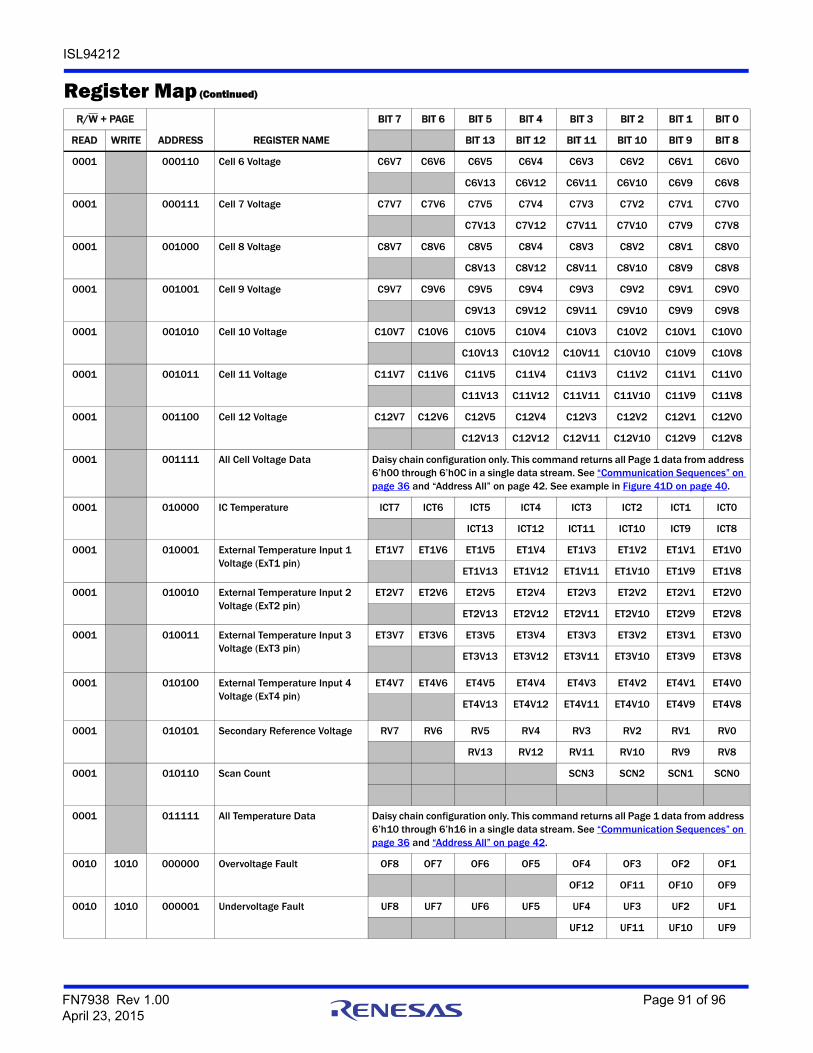
ISL94212
0001 000110 Cell 6 Voltage C6V7 C6V6 C6V5 C6V4 C6V3 C6V2 C6V1 C6V0
C6V13 C6V12 C6V11 C6V10 C6V9 C6V8
0001 000111 Cell 7 Voltage C7V7 C7V6 C7V5 C7V4 C7V3 C7V2 C7V1 C7V0
C7V13 C7V12 C7V11 C7V10 C7V9 C7V8
0001 001000 Cell 8 Voltage C8V7 C8V6 C8V5 C8V4 C8V3 C8V2 C8V1 C8V0
C8V13 C8V12 C8V11 C8V10 C8V9 C8V8
0001 001001 Cell 9 Voltage C9V7 C9V6 C9V5 C9V4 C9V3 C9V2 C9V1 C9V0
C9V13 C9V12 C9V11 C9V10 C9V9 C9V8
0001 001010 Cell 10 Voltage C10V7 C10V6 C10V5 C10V4 C10V3 C10V2 C10V1 C10V0
C10V13 C10V12 C10V11 C10V10 C10V9 C10V8
0001 001011 Cell 11 Voltage C11V7 C11V6 C11V5 C11V4 C11V3 C11V2 C11V1 C11V0
C11V13 C11V12 C11V11 C11V10 C11V9 C11V8
0001 001100 Cell 12 Voltage C12V7 C12V6 C12V5 C12V4 C12V3 C12V2 C12V1 C12V0
C12V13 C12V12 C12V11 C12V10 C12V9 C12V8
0001 001111 All Cell Voltage Data Daisy chain configuration only. This command returns all Page 1 data from address 6’h00 through 6’h0C in a single data stream. See “Communication Sequences” on page 36 and “Address All” on page 42. See example in Figure 41D on page 40.
0001 010000 IC Temperature ICT7 ICT6 ICT5 ICT4 ICT3 ICT2 ICT1 ICT0
ICT13 ICT12 ICT11 ICT10 ICT9 ICT8
0001 010001 External Temperature Input 1 Voltage (ExT1 pin)
ET1V7 ET1V6 ET1V5 ET1V4 ET1V3 ET1V2 ET1V1 ET1V0
ET1V13 ET1V12 ET1V11 ET1V10 ET1V9 ET1V8
0001 010010 External Temperature Input 2 Voltage (ExT2 pin)
ET2V7 ET2V6 ET2V5 ET2V4 ET2V3 ET2V2 ET2V1 ET2V0
ET2V13 ET2V12 ET2V11 ET2V10 ET2V9 ET2V8
0001 010011 External Temperature Input 3 Voltage (ExT3 pin)
ET3V7 ET3V6 ET3V5 ET3V4 ET3V3 ET3V2 ET3V1 ET3V0
ET3V13 ET3V12 ET3V11 ET3V10 ET3V9 ET3V8
0001 010100 External Temperature Input 4 Voltage (ExT4 pin)
ET4V7 ET4V6 ET4V5 ET4V4 ET4V3 ET4V2 ET4V1 ET4V0
ET4V13 ET4V12 ET4V11 ET4V10 ET4V9 ET4V8
0001 010101 Secondary Reference Voltage RV7 RV6 RV5 RV4 RV3 RV2 RV1 RV0
RV13 RV12 RV11 RV10 RV9 RV8
0001 010110 Scan Count SCN3 SCN2 SCN1 SCN0
0001 011111 All Temperature Data Daisy chain configuration only. This command returns all Page 1 data from address 6’h10 through 6’h16 in a single data stream. See “Communication Sequences” on page 36 and “Address All” on page 42.
0010 1010 000000 Overvoltage Fault OF8 OF7 OF6 OF5 OF4 OF3 OF2 OF1
OF12 OF11 OF10 OF9
0010 1010 000001 Undervoltage Fault UF8 UF7 UF6 UF5 UF4 UF3 UF2 UF1
UF12 UF11 UF10 UF9
Register Map (Continued)
R/W + PAGE
ADDRESS REGISTER NAME
BIT 7 BIT 6 BIT 5 BIT 4 BIT 3 BIT 2 BIT 1 BIT 0
READ WRITE BIT 13 BIT 12 BIT 11 BIT 10 BIT 9 BIT 8
FN7938 Rev 1.00 Page 91 of 96April 23, 2015
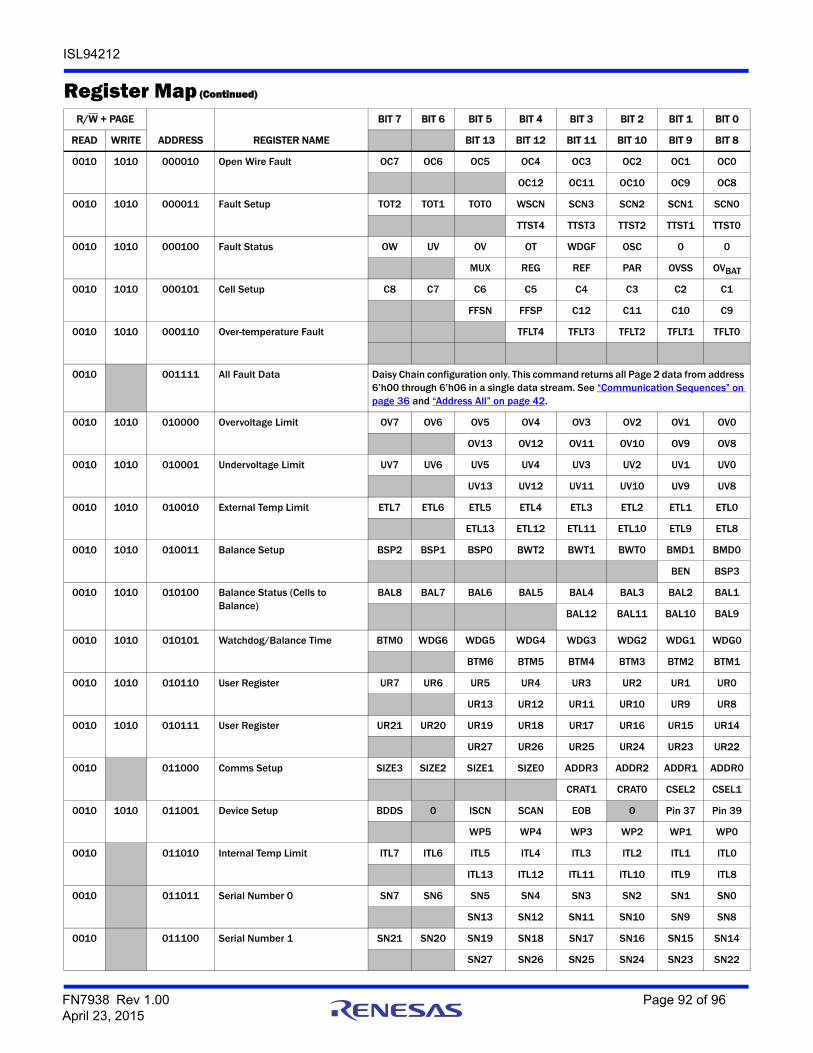
ISL94212
0010 1010 000010 Open Wire Fault OC7 OC6 OC5 OC4 OC3 OC2 OC1 OC0
OC12 OC11 OC10 OC9 OC8
0010 1010 000011 Fault Setup TOT2 TOT1 TOT0 WSCN SCN3 SCN2 SCN1 SCN0
TTST4 TTST3 TTST2 TTST1 TTST0
0010 1010 000100 Fault Status OW UV OV OT WDGF OSC 0 0
MUX REG REF PAR OVSS OVBAT
0010 1010 000101 Cell Setup C8 C7 C6 C5 C4 C3 C2 C1
FFSN FFSP C12 C11 C10 C9
0010 1010 000110 Over-temperature Fault TFLT4 TFLT3 TFLT2 TFLT1 TFLT0
0010 001111 All Fault Data Daisy Chain configuration only. This command returns all Page 2 data from address 6’h00 through 6’h06 in a single data stream. See “Communication Sequences” on page 36 and “Address All” on page 42.
0010 1010 010000 Overvoltage Limit OV7 OV6 OV5 OV4 OV3 OV2 OV1 OV0
OV13 OV12 OV11 OV10 OV9 OV8
0010 1010 010001 Undervoltage Limit UV7 UV6 UV5 UV4 UV3 UV2 UV1 UV0
UV13 UV12 UV11 UV10 UV9 UV8
0010 1010 010010 External Temp Limit ETL7 ETL6 ETL5 ETL4 ETL3 ETL2 ETL1 ETL0
ETL13 ETL12 ETL11 ETL10 ETL9 ETL8
0010 1010 010011 Balance Setup BSP2 BSP1 BSP0 BWT2 BWT1 BWT0 BMD1 BMD0
BEN BSP3
0010 1010 010100 Balance Status (Cells to Balance)
BAL8 BAL7 BAL6 BAL5 BAL4 BAL3 BAL2 BAL1
BAL12 BAL11 BAL10 BAL9
0010 1010 010101 Watchdog/Balance Time BTM0 WDG6 WDG5 WDG4 WDG3 WDG2 WDG1 WDG0
BTM6 BTM5 BTM4 BTM3 BTM2 BTM1
0010 1010 010110 User Register UR7 UR6 UR5 UR4 UR3 UR2 UR1 UR0
UR13 UR12 UR11 UR10 UR9 UR8
0010 1010 010111 User Register UR21 UR20 UR19 UR18 UR17 UR16 UR15 UR14
UR27 UR26 UR25 UR24 UR23 UR22
0010 011000 Comms Setup SIZE3 SIZE2 SIZE1 SIZE0 ADDR3 ADDR2 ADDR1 ADDR0
CRAT1 CRAT0 CSEL2 CSEL1
0010 1010 011001 Device Setup BDDS 0 ISCN SCAN EOB 0 Pin 37 Pin 39
WP5 WP4 WP3 WP2 WP1 WP0
0010 011010 Internal Temp Limit ITL7 ITL6 ITL5 ITL4 ITL3 ITL2 ITL1 ITL0
ITL13 ITL12 ITL11 ITL10 ITL9 ITL8
0010 011011 Serial Number 0 SN7 SN6 SN5 SN4 SN3 SN2 SN1 SN0
SN13 SN12 SN11 SN10 SN9 SN8
0010 011100 Serial Number 1 SN21 SN20 SN19 SN18 SN17 SN16 SN15 SN14
SN27 SN26 SN25 SN24 SN23 SN22
Register Map (Continued)
R/W + PAGE
ADDRESS REGISTER NAME
BIT 7 BIT 6 BIT 5 BIT 4 BIT 3 BIT 2 BIT 1 BIT 0
READ WRITE BIT 13 BIT 12 BIT 11 BIT 10 BIT 9 BIT 8
FN7938 Rev 1.00 Page 92 of 96April 23, 2015
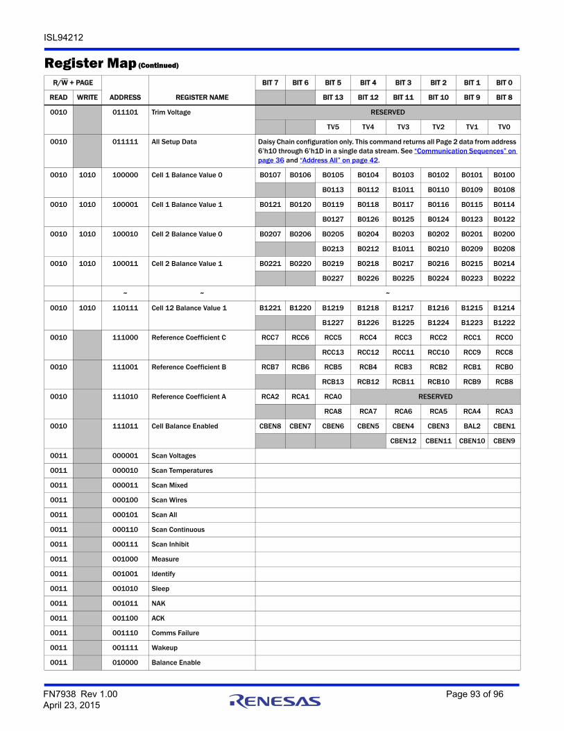
ISL94212
0010 011101 Trim Voltage RESERVED
TV5 TV4 TV3 TV2 TV1 TV0
0010 011111 All Setup Data Daisy Chain configuration only. This command returns all Page 2 data from address 6’h10 through 6’h1D in a single data stream. See “Communication Sequences” on page 36 and “Address All” on page 42.
0010 1010 100000 Cell 1 Balance Value 0 B0107 B0106 B0105 B0104 B0103 B0102 B0101 B0100
B0113 B0112 B1011 B0110 B0109 B0108
0010 1010 100001 Cell 1 Balance Value 1 B0121 B0120 B0119 B0118 B0117 B0116 B0115 B0114
B0127 B0126 B0125 B0124 B0123 B0122
0010 1010 100010 Cell 2 Balance Value 0 B0207 B0206 B0205 B0204 B0203 B0202 B0201 B0200
B0213 B0212 B1011 B0210 B0209 B0208
0010 1010 100011 Cell 2 Balance Value 1 B0221 B0220 B0219 B0218 B0217 B0216 B0215 B0214
B0227 B0226 B0225 B0224 B0223 B0222
~ ~ ~
0010 1010 110111 Cell 12 Balance Value 1 B1221 B1220 B1219 B1218 B1217 B1216 B1215 B1214
B1227 B1226 B1225 B1224 B1223 B1222
0010 111000 Reference Coefficient C RCC7 RCC6 RCC5 RCC4 RCC3 RCC2 RCC1 RCC0
RCC13 RCC12 RCC11 RCC10 RCC9 RCC8
0010 111001 Reference Coefficient B RCB7 RCB6 RCB5 RCB4 RCB3 RCB2 RCB1 RCB0
RCB13 RCB12 RCB11 RCB10 RCB9 RCB8
0010 111010 Reference Coefficient A RCA2 RCA1 RCA0 RESERVED
RCA8 RCA7 RCA6 RCA5 RCA4 RCA3
0010 111011 Cell Balance Enabled CBEN8 CBEN7 CBEN6 CBEN5 CBEN4 CBEN3 BAL2 CBEN1
CBEN12 CBEN11 CBEN10 CBEN9
0011 000001 Scan Voltages
0011 000010 Scan Temperatures
0011 000011 Scan Mixed
0011 000100 Scan Wires
0011 000101 Scan All
0011 000110 Scan Continuous
0011 000111 Scan Inhibit
0011 001000 Measure
0011 001001 Identify
0011 001010 Sleep
0011 001011 NAK
0011 001100 ACK
0011 001110 Comms Failure
0011 001111 Wakeup
0011 010000 Balance Enable
Register Map (Continued)
R/W + PAGE
ADDRESS REGISTER NAME
BIT 7 BIT 6 BIT 5 BIT 4 BIT 3 BIT 2 BIT 1 BIT 0
READ WRITE BIT 13 BIT 12 BIT 11 BIT 10 BIT 9 BIT 8
FN7938 Rev 1.00 Page 93 of 96April 23, 2015
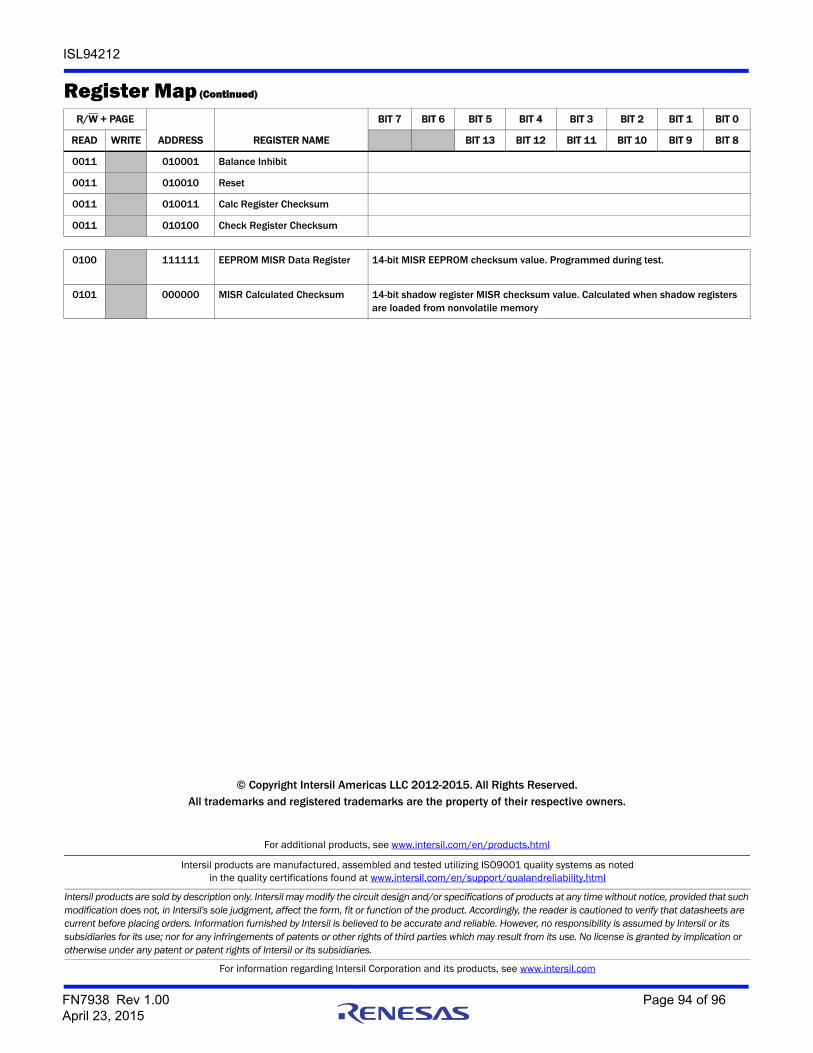
ISL94212
Intersil products are manufactured, assembled and tested utilizing ISO9001 quality systems as notedin the quality certifications found at www.intersil.com/en/support/qualandreliability.html
Intersil products are sold by description only. Intersil may modify the circuit design and/or specifications of products at any time without notice, provided that such modification does not, in Intersil's sole judgment, affect the form, fit or function of the product. Accordingly, the reader is cautioned to verify that datasheets are current before placing orders. Information furnished by Intersil is believed to be accurate and reliable. However, no responsibility is assumed by Intersil or its subsidiaries for its use; nor for any infringements of patents or other rights of third parties which may result from its use. No license is granted by implication or otherwise under any patent or patent rights of Intersil or its subsidiaries.
For information regarding Intersil Corporation and its products, see www.intersil.com
For additional products, see www.intersil.com/en/products.html
© Copyright Intersil Americas LLC 2012-2015. All Rights Reserved.All trademarks and registered trademarks are the property of their respective owners.
0011 010001 Balance Inhibit
0011 010010 Reset
0011 010011 Calc Register Checksum
0011 010100 Check Register Checksum
0100 111111 EEPROM MISR Data Register 14-bit MISR EEPROM checksum value. Programmed during test.
0101 000000 MISR Calculated Checksum 14-bit shadow register MISR checksum value. Calculated when shadow registers are loaded from nonvolatile memory
Register Map (Continued)
R/W + PAGE
ADDRESS REGISTER NAME
BIT 7 BIT 6 BIT 5 BIT 4 BIT 3 BIT 2 BIT 1 BIT 0
READ WRITE BIT 13 BIT 12 BIT 11 BIT 10 BIT 9 BIT 8
FN7938 Rev 1.00 Page 94 of 96April 23, 2015
ISL94212
About Intersil
Intersil Corporation is a leading provider of innovative power management and precision analog solutions. The company's products address some of the largest markets within the industrial and infrastructure, mobile computing and high-end consumer markets.
For the most updated datasheet, application notes, related documentation and related parts, please see the respective product information page found at www.intersil.com.
You may report errors or suggestions for improving this datasheet by visiting www.intersil.com/ask.
Reliability reports are also available from our website at www.intersil.com/support
Revision HistoryThe revision history provided is for informational purposes only and is believed to be accurate, but not warranted. Please go to web to make sure you have the latest Rev.
DATE REVISION CHANGE
April 23, 2015 FN7938.1 Changed ground references in Figure 1 on page 1.Abs Max “Absolute Maximum Ratings” on page 7 changed the text in the ESD Ratings from Capacitive Discharge to Charge Device Model“Recommended Operating Conditions” on page 7 moved ExT1, ExT2, ExT3, ExT4, which had voltage range 0V to 3.6V to separate line with voltage range 0V to 2.5V. Added to “BASE” in “Pin Descriptions” on page 5, “Do not let this pin float.” Table 3 on page 24, Changed “Cell 0 Voltage” to “VBAT Voltage”.Section , “CRC Calculation,” on page 36: Added example software CRC calculation code (Figure 39 on page 37.)Section , “Reset,” on page 42 - Added note: “A Reset command should be issued following a “hard reset” in which the EN pin is toggled.”Changed “Fault Signal Filtering” on page 46 to add the comment in 2nd paragraph, “When a fault is detected, the [TOT2:0] bits should be rewritten.”Table 30 on page 47, changed in comments for “Read checksum value calculated by ISL94212” from: ...“cycling the EN pin or the host issuing a Reset command.” to: ...“cycling the EN pin followed by a host initiated Reset command,or simply the host issuing a Reset command.”Changed Section, “System Registers,” on page 62. Changed in 4th paragraph 1st sentence “when the EN pin is low” to “when the EN pin is toggled and the device receives a Reset Command”.Section, “Register Descriptions,” on page 62: Changed “Cell 0 Voltage” to “VBAT Voltage” and added voltage calculation equations.System Register description “TOT0, 1, 2” on page 64 added the comment, “This register must be re-written following an error detection resulting from totalizer overflow.”Added to last sentence 2nd paragraph in Section, “Power Supplies,” on page 82, “The external pass transistor is required. Do not allow this pin to float.”Changed all pin name references to all caps.Updated Definitions for Shutdown Mode in “Power Modes” on page 21 and “Reset” on page 42.Table 50 on page 84, Updated recommendation for C1Replaced “Measurement and Communication Timing” Section (pages 51 to 58 of previous document) with new sections “Communication and Measurement Diagrams” on page 50 and “Communication and Measurement Timing Tables” on page 56 with new figures and tables to offer more clarity and flexibility in communication and measurement timing calculations.
December 14, 2012 FN7938.0 Initial Release.
FN7938 Rev 1.00 Page 95 of 96April 23, 2015
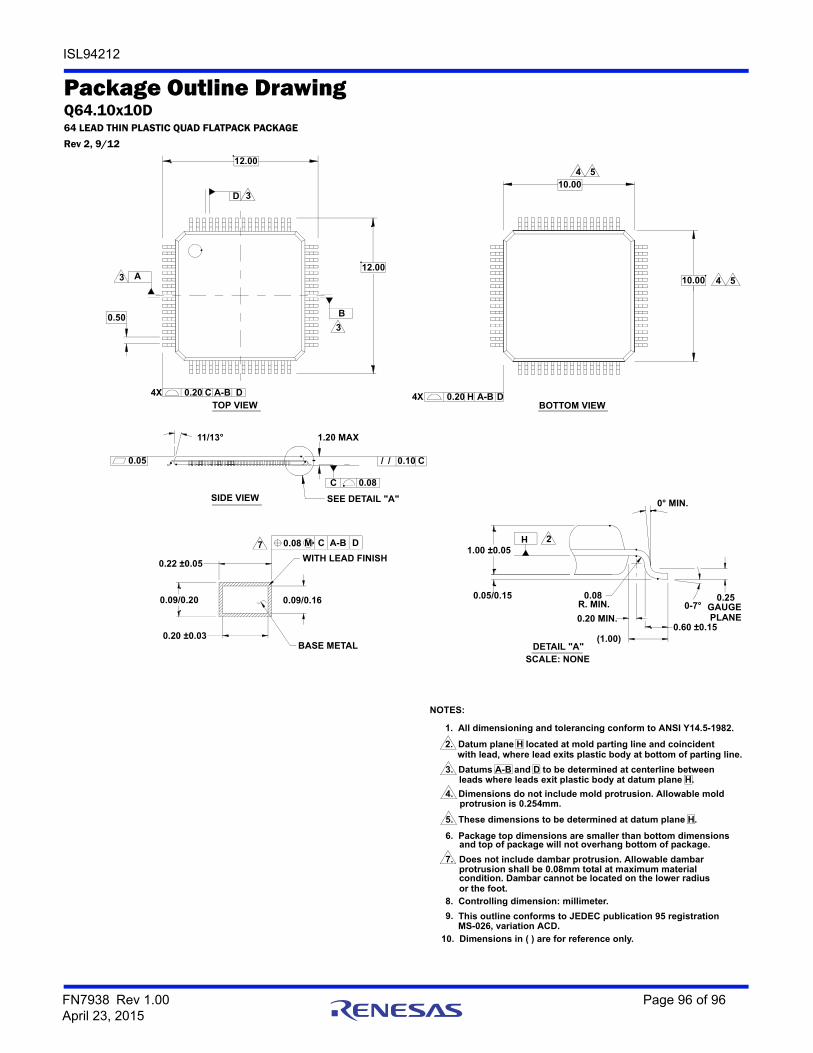
ISL94212
FN7938 Rev 1.00 Page 96 of 96April 23, 2015
Package Outline DrawingQ64.10x10D64 LEAD THIN PLASTIC QUAD FLATPACK PACKAGE
Rev 2, 9/12
BOTTOM VIEW
DETAIL "A"
SIDE VIEW
TOP VIEW
NOTES:
MS-026, variation ACD.
8. Controlling dimension: millimeter.
This outline conforms to JEDEC publication 95 registration
condition. Dambar cannot be located on the lower radius protrusion shall be 0.08mm total at maximum material Does not include dambar protrusion. Allowable dambar
6. Package top dimensions are smaller than bottom dimensions and top of package will not overhang bottom of package.
1. All dimensioning and tolerancing conform to ANSI Y14.5-1982.
2. Datum plane H located at mold parting line and coincident with lead, where lead exits plastic body at bottom of parting line.
3. Datums A-B and D to be determined at centerline between leads where leads exit plastic body at datum plane H.
4. Dimensions do not include mold protrusion. Allowable mold protrusion is 0.254mm.
9.
7.
5. These dimensions to be determined at datum plane H.
10. Dimensions in ( ) are for reference only.
or the foot.
0.20 MIN.
(1.00)
0.09/0.20
0.20 ±0.03BASE METAL
0.09/0.16
7
0.22 ±0.05
0.05
11/13°
WITH LEAD FINISH
0.08 CM A-B D
0.05/0.15R. MIN.
0.08
SEE DETAIL "A"
C 0.08
1.20 MAX
// 0.10 C
1.00 ±0.05
H
GAUGE
0.60 ±0.15
0-7°0.25
0° MIN.
4X
0.50
C A-B D0.20
3 A
0.204X
3
A-BH D
5
B
4
D 3
12.00
10.004 5
12.00
10.00
2
SCALE: NONE
PLANE