Embed Size (px)
Citation preview

Isolated 6SW 3Phase 2A Gate Drive Module
GDS-2A6S1
Applications
Features
• 6 Switch Isolated
IGBT/MOSFET Gate
Drive
• AC & Brushless DC
Motor Drives
• 3 Phase PFC Rectifiers
• R&D Inverters
• Very Low Propagation Delay of
75ns Maximum.
• Low Distortion at Extremely
High Frequency Operation.
• PWM, High/Low Side and Dual
Inputs Versions
• Input & Output Indication
LEDs for Visual Feedback.
• Input & Output Test points for
easy testing.
• Built-in 5V Regulator for
Powering up External Control
Circuitry.
• Best Cost to Performance
Ratio in the Market.
• Suitable for 1200V IGBTs and
Power MOSFETs.
• 2A Peak Gate Drive Current.
• 3000 VRMS Input to Output
Isolation.
• Output UVLO Protection.
• Output Clamping Protection.
• Configurable Dead-Time.
• 20KV/us Minimum Common
Mode Rejection (CMR).
Description
The GDS-2A6S1 is high performance fully isolated IGBT/MOSFET gate
drive module for 3 Phase 6 Switch configuration. It is specially designed
for fastest power electronics prototyping in research and educational
environments. The drive use’s Silicon Lab’s Si823x high performance gate
driver IC, and feature’s dead time generation logic, overlap protection,
input and output indication LEDs, test points and built in 5V regulator
which could be used to power up external control circuitry.
But the most notable feature of this module is its extremely low
propagation delay of less than 75ns. This is particularly important for very
high switching frequency applications such as ZVS and ZCS topologies,
it’s also ideal for cascaded and parallel topologies to minimize differences
between switches. Overall, this module will achieve fastest gate drive
operation and lowest output signal distortion.
This product can be ordered with different input and output connectors,
making it suitable as a plugin module, PCB mounted module or free
hanging module.
Compliance
• ROHS
Page 2
GDS-2A6S1
DATASHEET
Version Release Date Changes
1.0 17/08/2015 First Version Released
Revision History Table
WARNING AND DISCLAIMER !
ATTENTION PLEASE! THE INFORMATION HEREIN IS GIVEN TO DESCRIBE CERTAIN COMPONENTS AND SHALL NOT BE CONSIDERED AS A GUARANTEE
OF CHARACTERISTICS. TERMS OF DELIVERY AND RIGHTS TO TECHNICAL CHANGE RESERVED. WE HEREBY DISCLAIM ANY AND ALL WARRANTIES,
INCLUDING BUT NOT LIMITED TO WARRANTIES OF NON-INFRINGEMENT, REGARDING CIRCUITS, DESCRIPTIONS AND CHARTS STATED HEREIN.
CUSTOMER IS SOLELY RESPONSIBLE OF PROPER AND LEGAL USE OF ALL PRODUCTS OFFERED BY TARAZ TECHNOLOGIES.
SAFETY NOTICE !
ATTENTION PLEASE! THIS DEVICE IS ESD SENSITIVE AND NEEDS TO BE HANDLED WITH CARE. HIGH VOLTAGE CONDITION MAY OCCUR DURING
OPERATION OF THE DEVICE, AND HENCE USER IS SOLELY RESPONSIBLE OF EQUIPMENT AND PERSONNEL SAFETY. TARAZ TECHNOLOGIES SHALL
NOT BE HOLD LIABLE FOR ANY DAMAGE TO PERSONNEL AND/OR PROPERTIES AS A RESULT OF USING THIS DEVICE. USER MUST TAKE ADEQUATE
STEPS TO ENSURE ELECTRICAL AND MECHANICAL SAFETLY OF THE DEVICE IN USE.
Page 3
GDS-2A6S1
DATASHEET
Features ...................................................................................................................................................................................................................... 1
Description ................................................................................................................................................................................................................ 1
Compliance ............................................................................................................................................................................................................... 1
Applications .............................................................................................................................................................................................................. 1
Revision History Table .......................................................................................................................................................................................... 2
WARNING AND DISCLAIMER ! ........................................................................................................................................................................... 2
SAFETY NOTICE ! ..................................................................................................................................................................................................... 2
Table of Contents ................................................................................................................................................................................................... 3
Ratings & Characteristics .................................................................................................................................................................................... 4
Ratings & Characteristics (Continued) .......................................................................................................................................................... 5
Block Diagram .......................................................................................................................................................................................................... 6
Pin Description ........................................................................................................................................................................................................ 7
Application Information ...................................................................................................................................................................................... 8
Typical Application Circuit ............................................................................................................................................................................... 8
Operation Requirements .................................................................................................................................................................................. 8
Power Supply & Configuration (J2, J3& J4) ................................................................................................................................................. 8
PWM, High/Low and Dual Driver Versions ................................................................................................................................................. 8
Application Information (Continued) ........................................................................................................................................................... 9
Input & Output Indication LEDs, Test Points .............................................................................................................................................. 9
Mounting and Safety .......................................................................................................................................................................................... 9
Mechanical Drawing ........................................................................................................................................................................................... 10
Ordering Information ......................................................................................................................................................................................... 11
Table of Contents
Page 4
GDS-2A6S1
DATASHEET
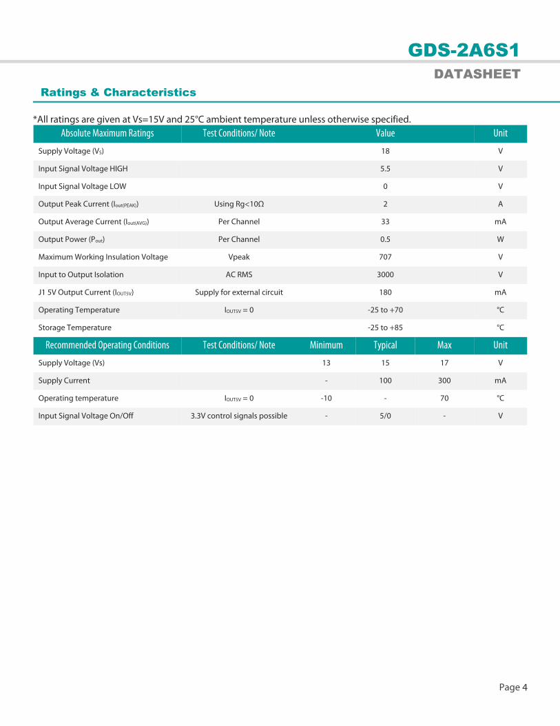
*All ratings are given at Vs=15V and 25°C ambient temperature unless otherwise specified.
Absolute Maximum Ratings Test Conditions/ Note Value Unit
Supply Voltage (VS) 18 V
Input Signal Voltage HIGH 5.5 V
Input Signal Voltage LOW 0 V
Output Peak Current (Iout(PEAK)) Using Rg<10Ω 2 A
Output Average Current (Iout(AVG)) Per Channel 33 mA
Output Power (Pout) Per Channel 0.5 W
Maximum Working Insulation Voltage Vpeak 707 V
Input to Output Isolation AC RMS 3000 V
J1 5V Output Current (IOUT5V) Supply for external circuit 180 mA
Operating Temperature IOUT5V = 0 -25 to +70 °C
Storage Temperature -25 to +85 °C
Recommended Operating Conditions Test Conditions/ Note Minimum Typical Max Unit
Supply Voltage (Vs) 13 15 17 V
Supply Current - 100 300 mA
Operating temperature IOUT5V = 0 -10 - 70 °C
Input Signal Voltage On/Off 3.3V control signals possible - 5/0 - V
Ratings & Characteristics
Page 5
GDS-2A6S1
DATASHEET
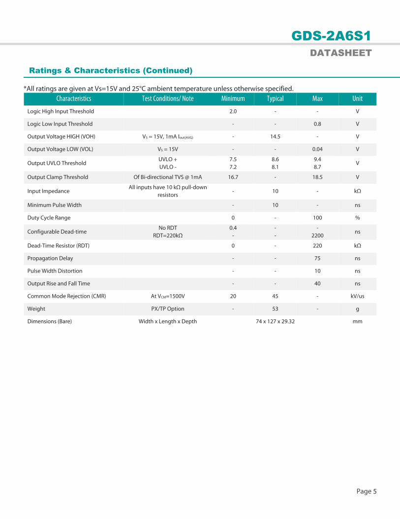
*All ratings are given at Vs=15V and 25°C ambient temperature unless otherwise specified.
Characteristics Test Conditions/ Note Minimum Typical Max Unit
Logic High Input Threshold 2.0 - - V
Logic Low Input Threshold - - 0.8 V
Output Voltage HIGH (VOH) VS = 15V, 1mA Iout(AVG) - 14.5 - V
Output Voltage LOW (VOL) VS = 15V - - 0.04 V
Output UVLO Threshold UVLO +
UVLO -
7.5
7.2
8.6
8.1
9.4
8.7 V
Output Clamp Threshold Of Bi-directional TVS @ 1mA 16.7 - 18.5 V
Input Impedance All inputs have 10 kΩ pull-down
resistors - 10 - kΩ
Minimum Pulse Width - 10 - ns
Duty Cycle Range 0 - 100 %
Configurable Dead-time No RDT
RDT=220kΩ
0.4
-
-
-
-
2200 ns
Dead-Time Resistor (RDT) 0 - 220 kΩ
Propagation Delay - - 75 ns
Pulse Width Distortion - - 10 ns
Output Rise and Fall Time - - 40 ns
Common Mode Rejection (CMR) At VCM=1500V 20 45 - kV/us
Weight PX/TP Option - 53 - g
Dimensions (Bare) Width x Length x Depth 74 x 127 x 29.32 mm
Ratings & Characteristics (Continued)
Page 6
GDS-2A6S1
DATASHEET
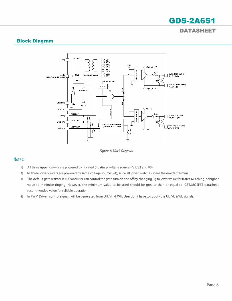
Figure 1: Block Diagram
Notes:
1) All three upper drivers are powered by isolated (floating) voltage sources (V1, V2 and V3).
2) All three lower drivers are powered by same voltage source (V4), since all lower switches share the emitter terminal.
3) The default gate resistor is 10Ω and user can control the gate turn on and off by changing Rg to lower value for faster switching, or higher
value to minimize ringing. However, the minimum value to be used should be greater than or equal to IGBT/MOSFET datasheet
recommended value for reliable operation.
4) In PWM Driver, control signals will be generated from UH, VH & WH. User don’t have to supply the UL, VL & WL signals.
Block Diagram
Page 7
GDS-2A6S1
DATASHEET
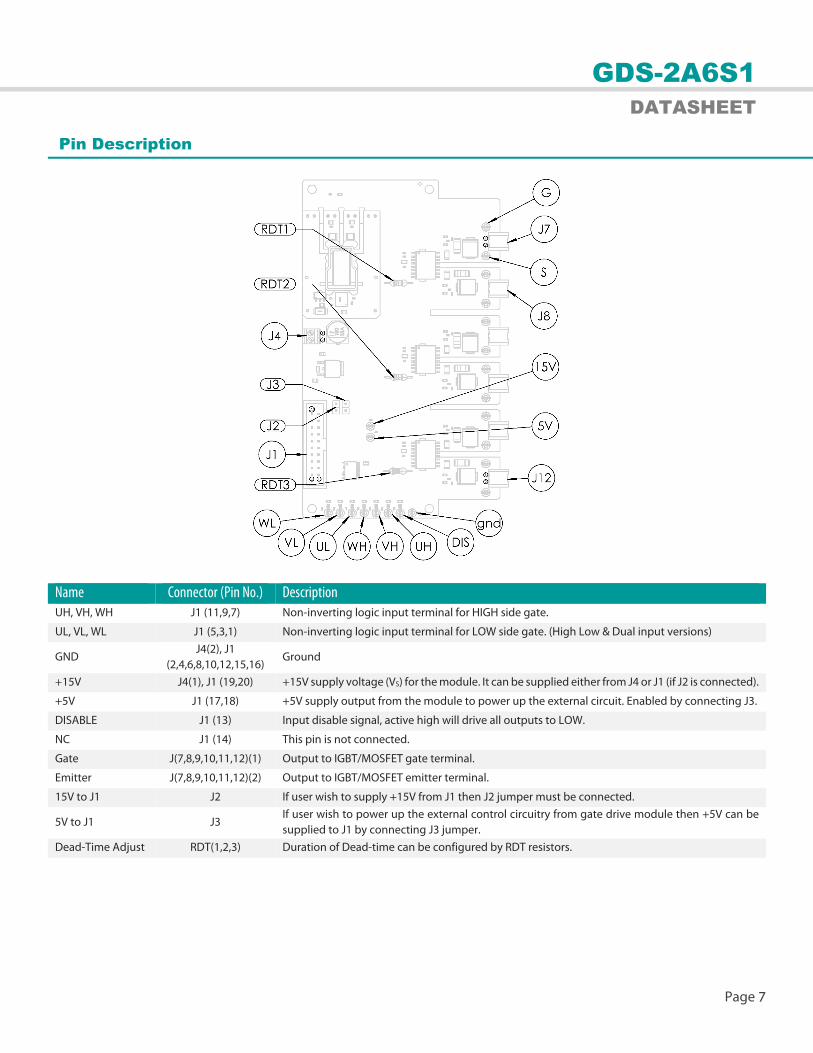
Name Connector (Pin No.) Description
UH, VH, WH J1 (11,9,7) Non-inverting logic input terminal for HIGH side gate.
UL, VL, WL J1 (5,3,1) Non-inverting logic input terminal for LOW side gate. (High Low & Dual input versions)
GND J4(2), J1
(2,4,6,8,10,12,15,16) Ground
+15V J4(1), J1 (19,20) +15V supply voltage (VS) for the module. It can be supplied either from J4 or J1 (if J2 is connected).
+5V J1 (17,18) +5V supply output from the module to power up the external circuit. Enabled by connecting J3.
DISABLE J1 (13) Input disable signal, active high will drive all outputs to LOW.
NC J1 (14) This pin is not connected.
Gate J(7,8,9,10,11,12)(1) Output to IGBT/MOSFET gate terminal.
Emitter J(7,8,9,10,11,12)(2) Output to IGBT/MOSFET emitter terminal.
15V to J1 J2 If user wish to supply +15V from J1 then J2 jumper must be connected.
5V to J1 J3 If user wish to power up the external control circuitry from gate drive module then +5V can be
supplied to J1 by connecting J3 jumper.
Dead-Time Adjust RDT(1,2,3) Duration of Dead-time can be configured by RDT resistors.
Pin Description
Page 8
GDS-2A6S1
DATASHEET
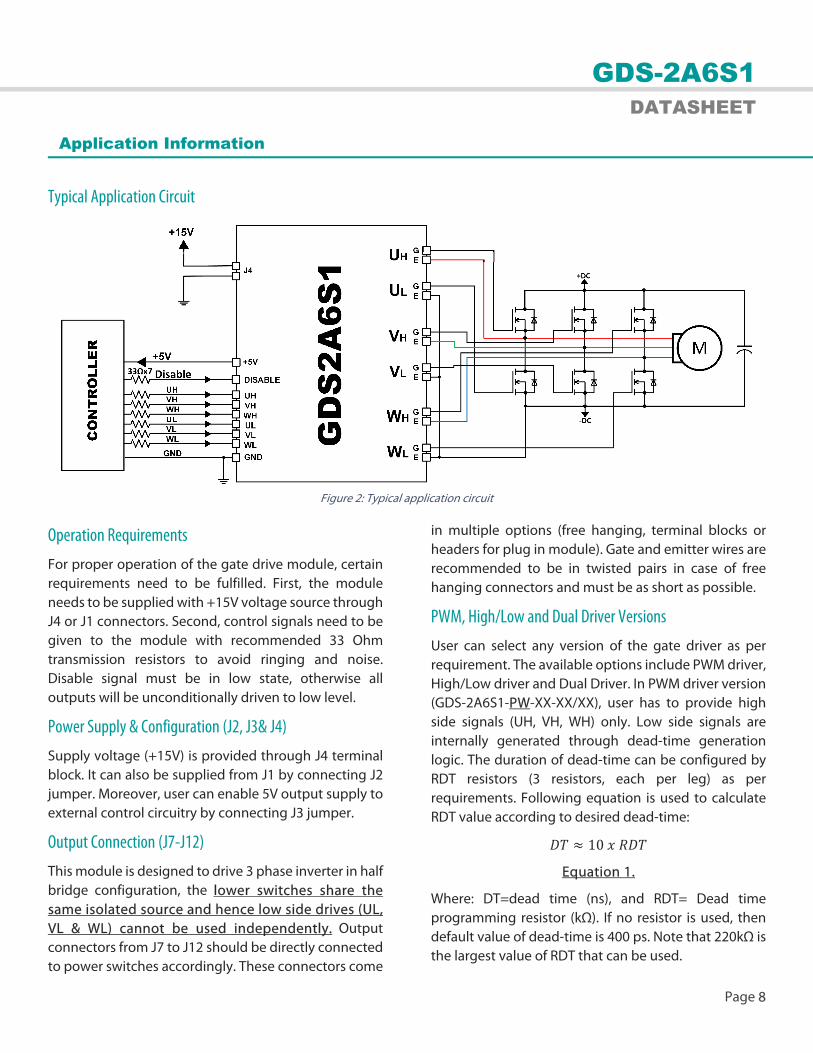
Typical Application Circuit
Operation Requirements
For proper operation of the gate drive module, certain
requirements need to be fulfilled. First, the module
needs to be supplied with +15V voltage source through
J4 or J1 connectors. Second, control signals need to be
given to the module with recommended 33 Ohm
transmission resistors to avoid ringing and noise.
Disable signal must be in low state, otherwise all
outputs will be unconditionally driven to low level.
Power Supply & Configuration (J2, J3& J4)
Supply voltage (+15V) is provided through J4 terminal
block. It can also be supplied from J1 by connecting J2
jumper. Moreover, user can enable 5V output supply to
external control circuitry by connecting J3 jumper.
Output Connection (J7-J12)
This module is designed to drive 3 phase inverter in half
bridge configuration, the lower switches share the
same isolated source and hence low side drives (UL,
VL & WL) cannot be used independently. Output
connectors from J7 to J12 should be directly connected
to power switches accordingly. These connectors come
in multiple options (free hanging, terminal blocks or
headers for plug in module). Gate and emitter wires are
recommended to be in twisted pairs in case of free
hanging connectors and must be as short as possible.
PWM, High/Low and Dual Driver Versions
User can select any version of the gate driver as per
requirement. The available options include PWM driver,
High/Low driver and Dual Driver. In PWM driver version
(GDS-2A6S1-PW-XX-XX/XX), user has to provide high
side signals (UH, VH, WH) only. Low side signals are
internally generated through dead-time generation
logic. The duration of dead-time can be configured by
RDT resistors (3 resistors, each per leg) as per
requirements. Following equation is used to calculate
RDT value according to desired dead-time:
≈ 10
Equation 1.
Where: DT=dead time (ns), and RDT= Dead time
programming resistor (kΩ). If no resistor is used, then
default value of dead-time is 400 ps. Note that 220kΩ is
the largest value of RDT that can be used.
Application Information
Figure 2: Typical application circuit

Page 9
GDS-2A6S1
DATASHEET
In High/Low Driver version (GDS-2A6S1-HL-XX-XX/XX),
both switches of the leg are controlled through their
respective signals. This module comes with built-in
overlap protection to prevent same phase outputs (e.g.,
UH & UL) from being high at the same time. The dead-
time is user adjusted using RDT configuration resistors
using Equation 1.
In Dual Driver version (GDS-2A6S1-DL-XX-XX/XX), all
channels are independently controlled through
respective signals, this is required for some topologies
where shoot-through is needed such as Z-Source
Inverter. Following table illustrate discussed versions.
PWM Version Inputs Outputs
UH UL Disable UOH UOL
L X L L H
H X L H L
X X H L L
High/Low Version Inputs Outputs
UH UL Disable UOH UOL
L L L L L
L H L L H
H L L H L
H H L L L
X X H L L
Dual Version Inputs Outputs
UH UL Disable UOH UOL
L L L L L
L H L L H
H L L H L
H H L H H
X X H L L
Input & Output Indication LEDs, Test Points
LEDs are provided on input and output signals for
instant user feedback. Input side LEDs are yellow
colored. While output LEDs are independent for ON
(Orange) state and OFF (Yellow) state so user can have
feedback of high frequency PWM signals as well.
Separate LEDs also indicate DISABLE (Orange) and
Power state (Green).
The module can also be supplied with input and output
test points for easy debugging. This is very helpful
feature for educational and research use. Test points are
available on all inputs, Disable, Power (+15V, +5V, GND)
and Gate, Emitter of all outputs.
Mounting and Safety
Since output side may carry dangerous high voltage, it
is not safe to touch the circuit in operation. User must
consider proper clearance of heat sink, metal enclosure,
stray metallic objects near output side, and cover
module and inverter with proper insulated casing. Care
must be taken with mounting since mounting holes are
close to outputs.
For more information, get our Application Note on how to design Three Phase Inverter to be used with our gate drive modules.
Visit: www.taraztechnologies.com
Application Information (Continued)
Page 10
GDS-2A6S1
DATASHEET
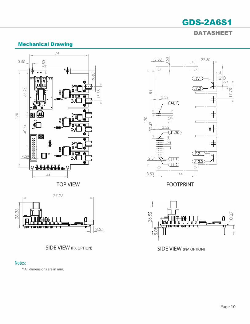
Notes: * All dimensions are in mm.
Mechanical Drawing
TOP VIEW
SIDE VIEW (PX OPTION)
FOOTPRINT
SIDE VIEW (PM OPTION)
GDS-2A6S1
DATASHEET
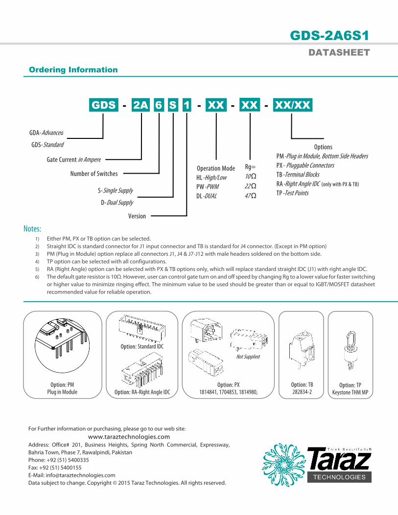
Notes: 1) Either PM, PX or TB option can be selected.
2) Straight IDC is standard connector for J1 input connector and TB is standard for J4 connector. (Except in PM option)
3) PM (Plug in Module) option replace all connectors J1, J4 & J7-J12 with male headers soldered on the bottom side.
4) TP option can be selected with all configurations.
5) RA (Right Angle) option can be selected with PX & TB options only, which will replace standard straight IDC (J1) with right angle IDC.
6) The default gate resistor is 10Ω. However, user can control gate turn on and off speed by changing Rg to a lower value for faster switching
or higher value to minimize ringing effect. The minimum value to be used should be greater than or equal to IGBT/MOSFET datasheet
recommended value for reliable operation.
For Further information or purchasing, please go to our web site:
www.taraztechnologies.com
Address: Office# 201, Business Heights, Spring North Commercial, Expressway,
Bahria Town, Phase 7, Rawalpindi, Pakistan
Phone: +92 (51) 5400335
Fax: +92 (51) 5400155
E-Mail: [email protected]
Data subject to change. Copyright © 2015 Taraz Technologies. All rights reserved.
Ordering Information
GDS - 2A 6 S 1 - XX - XX - XX/XX
GDA-Advanced
GDS-Standard
Gate Current in Ampere
Number of Switches
S-Single Supply
D-Dual Supply
Version
Operation Mode
HL-High/Low
PW-PWM
DL-DUAL
Rg=
10 Ω
22 Ω
47 Ω
Options
PM-Plug in Module, Bottom Side Headers
PX- Pluggable Connectors
TB-Terminal Blocks
RA-Right Angle IDC (only with PX & TB)
TP-Test Points
Option: TP Keystone THM MP
Option: TB 282834-2
Option: PX 1814841, 1704853, 1814980,
Option: Standard IDC
Option: RA-Right Angle IDC Option: PM
Plug in Module
Not Supplied