Embed Size (px)
Citation preview
ISSN No: 2348-4845International Journal & Magazine of Engineering,
Technology, Management and ResearchA Peer Reviewed Open Access International Journal
Volume No: 2 (2015), Issue No: 9 (September) September 2015 www.ijmetmr.com Page 217
Abstract:
In the field of Electronic Warfare (EW), interception of RADAR signals and disruption of RADAR performance are of primary importance. With the present day modern RADARs complex waveform modulations are being in-corporated to carry out Target detection and monitoring. Simulating these types of RADAR modulation wave-forms will help in proper interception of the RADARs for identification and evaluation of EW equipment. Based on Direct Digital Modulation method called DDS tech-nique, different types of RADAR waveforms and scan patterns are generated. This paper involves in the genera-tion of Intra Pulse Modulation i.e., Pulse compression in terms of both Frequency Modulation(Chirp) and Phase Modulation(Barker Code),Staggered PRI, Frequency Agility type of waveforms. It also generates replica of different types of antenna scan patterns for searching RA-DAR. This is will be realized in a Virtex-4 FPGA based board with DAC and associated logic circuits connected externally. Based on the resources available in Virtex 4 FPGA, MicroBlaze processor is configured by using Em-bedded Development Kit Tool.
Keywords:
Direct Digital Synthesis, MicroBlaze processor, Embed-ded Development Kit tool, Virtex-4 FPGA.
I.INTRODUCTION:
Rapid development of RADAR technology increases gradually the requirement for target detection which in turn relies much on signal waveforms. Therefore, various kinds of complicated waveforms have been generated. They have different influence on radars so that it is neces-sary to select them according to applications. On the other hand, radar countermeasure activities, appearing with ra-dar application, always devotes to interception, capture,
K.TejashwiniPG Scholar,
Department of ECE, Sree Nidhi Institute of Science & Technology,
Hyderabad, India.
G.V.Maha LakshmiProfessor,
Sree Nidhi Institute of Science & Technology, Hyderabad, India.
selection and recognition of desired radar signals in order to employ effective countermeasure. Generally, knowl-edge about signal waveforms is important both for radar and its counter measure. Techniques for generating arbi-trarily complicated waveforms have been updated from analog to digital ones. The aim of this project is to im-plement DDS technique on a Field Programmable Gate Array (FPGA).FPGA behaves according to a logic func-tion written in VERILOG/VHDL. The DDS technique programmed can be downloaded onto the FPGA as many times as wanted, there is no limit with different function-alities each time. At present, digital circuits and intelligent techniques are well developed, and direct digital synthe-sis (DDS) is widely applied [1-4]. Combined with other high speed digital control circuit, DDS is able to produce wideband complicated signals[4-8].
Pulse compression [9-11] allows radar to achieve the av-erage transmitted power of a relatively long pulse, while obtaining the range resolution of short pulse. In radar where there are limitations on the peak power, pulse com-pression is the only means to obtain the resolution and ac-curacy associated with a sharp pulse but at the same time acquiring the detection capability of a long pulse. Analog techniques to generate radar test signals are used. In this setup, multiple function generators with basic functional-ity are used to drive the Pulse, AM, FM, and Sweep in-puts of an analog signal generator. Using this setup a va-riety of radar test signals can be generated, ranging from pulsed CW to shaped pulses using AM to complex chirps using FM and Sweep. This is adequate for some applica-tions, however the pulse shaping capability is limited and managing the timing relationships associated with puls-ing modulated signals can be complicated. Because of the system complexity, there is also a high cost associated with calibrating and maintaining a system like this. The advantages of FPGAs are the possibility to reprogram the logic in case of errors in the design, faster prototyping that will lead to shorter design time and a lower cost per unit for small series.
FPGA Based RADAR Waveform Generator and Scan Pattern Simulator
Most FPGA vendors provide a long list of ready-to-use functional blocks, so called Intellectual Property (IP) blocks. The latest FPGAs can also be bought with one or more embedded processors, in form of hard proces-sor cores or as licenses for soft processor cores. This will speed up the design phase and of course also decrease the crucial time to market even more.In Section 2, DDS technology discussed briefly. Section 3 presents the Im-plementation Design. Section 4 proposes the adaptive spectrum sensing scheme. In Section 5, we analyzes the scheme from the viewpoint of detection performance and mean detection time simulation results and their detailed analysis and finally conclusions are drawn in Section 6.
II.DDS Technology:
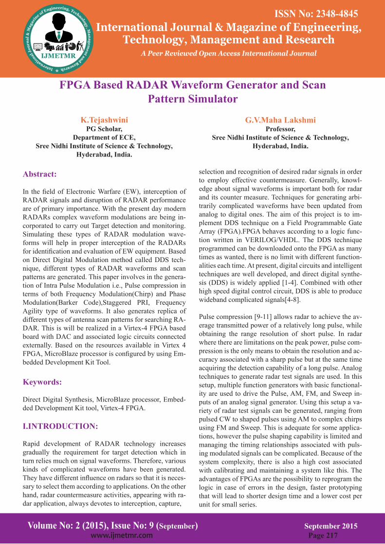
The basic function of a Direct Digital Synthesizer is straightforward as seen in fig 1. A lookup table holds a digital representation of the desired waveform over one period, with each row of the table containing a sample of the waveform’s amplitude. A system controller steps through this lookup table at a specific rate, feeding its value of the current row to the input of a DAC. When the controller reaches the end of the lookup table it cycles back to the first row and repeats the process. This process results in the desired analog signal appearing on the out-put of the DAC. Since no time consuming calculations are needed during signal generation this is a notably fast tech-nique. The output frequency can be changed by altering the values in the lookup table or reading from a separate lookup table.
Fig 1 Direct Digital Synthesizer
ISSN No: 2348-4845International Journal & Magazine of Engineering,
Technology, Management and ResearchA Peer Reviewed Open Access International Journal
Volume No: 2 (2015), Issue No: 9 (September) September 2015 www.ijmetmr.com Page 218
The Logic CORE™ IP DDS (Direct Digital Synthesizer) Compiler core sources sinusoidal waveforms for use in many applications. A DDS consists of a Phase Generator and a SIN/COS Lookup Table. These parts are available individually or combined via this core. Direct digital syn-thesis (DDS) is a method of producing an analog wave-form, usually a sine wave by generating a time-varying signal in digital form and then performing a digital-to- an-alog conversion. Because operations within a DDS device are primarily digital, it can offer fast switching between output frequencies, fine frequency resolution, and opera-tion over a broad spectrum of frequencies. With advances in design and process technology, today’s DDS devices are very compact and draw little power. When configured as a Sin/Cos LUT, the Phase Genera-tor is not implemented, and the phase is input via the PHASE_IN port, and transformed into the sine and co-sine outputs using a look-up table. Efficient memory us-age is achieved using half wave and quarter wave storage schemes. The presence of both outputs and their negation are configurable when the core is customized. Precision can be increased using optional Taylor Series Correction.Another possible choice is to use an FPGA with a soft core. With this method, the FPGA is configured to operate as a reduced instruction set (RISC) processor. Software can then be written for this processor in assembly or even the C programming language. We would then write a pro-gram to implement a DDS system and load it onto the FPGA/RISC processor.
III.IMPLEMENTATION DESIGN:
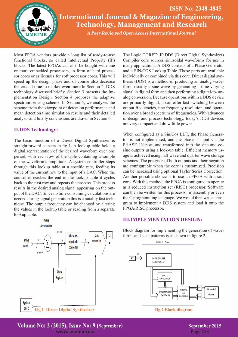
Block diagram for implementing the generation of wave-forms and scan patterns is as shown in figure 2.
Fig 2 Block diagram

ISSN No: 2348-4845International Journal & Magazine of Engineering,
Technology, Management and ResearchA Peer Reviewed Open Access International Journal
Volume No: 2 (2015), Issue No: 9 (September) September 2015 www.ijmetmr.com Page 219
This project will be realized in a Virtex-4 FPGA based board with DAC and associated logic circuits connected externally. Based on the resources available in Virtex-4 FPGA, MicroBlaze processor is configured by using Embedded Development Kit Tool. The software for generation of RF carrier will be implemented using Di-rect Digital Synthesis (DDS) and the complex RADAR waveforms and scan patterns [12] replica for pyramidal horn antenna are generated using VHDL/VERILOG and implemented in Virtex-4 FPGA. Waveform parameters like phase, frequency, PRI/PRF, Pulse Width are loaded in latches implemented in FPGA. Required data to gener-ate waveforms and scan patterns are entered in PC. These parameters are sent to MicroBlaze processor through GUI. If there is any pulse modulation required it is done and sent to DDS block. Antenna Scan Modulation Block consists of a Look Up Table, holding the E-plane and H-plane values of pyramidal horn antenna radiation pattern based on function of polar angles .For this pyramidal horn antenna is designed virtually and based in this dimensions radiation pattern is obtained by using respective equations in [13]. If we want particular scan pattern to be generated then that specific scan pattern VHDL/VERILOG code written is implemented in FPGA i.e., digital data obtained from DDS is multiplied with Antenna Scan Modulation Look Up Table samples to DAC. This generates particular scan pattern replica on CRO without physical existence of antenna here. If we want only waveform to be generated then this Antenna Scan Modulation block is deactivated i.e., Digital data obtained from DDS is sent to DAC by-passing Antenna Scan Modulation block.
Advantage of the above mentioned waveform generator in general, is the stability. Unlike the analogue circuits with discrete components with variable tolerances, these digital waveform synthesizers produce stable frequencies. Required waveform with sufficient bandwidth at desired Intermediate Frequencies (IF) could be generated using these platforms. This could be followed by an up conver-sion to the final RF band, amplification and transmission. The DDS signal generation technique is theoretically based on Nyquist Sampling Theorem. It could be seen as the inverse process of the signal sampling[14]. The sam-pling data of the required signals are calculated and stored in a Look-Up-Table (LUT), in which data are reachable by the phase codes. Sampling data are read out of the LUT and converted to analog signals through Digital-to-Analog Converter (DAC). Finally, required radar wave-form and scan pattern replica for pyramidal horn antenna is obtained after the DAC operation.
The directly digital modulation method samples the fre-quency modulation or phase modulation function of sig-nals, and saves the samples into frequency/phase ROM of DDS control circuit. Under the trigger of clock signal, the samples in the ROM are read into frequency/phase control registers. The DDS circuit outputs signals with modulation desired according to data in the registers, un-der the control of system clock. Most of popular digital waveform generating system employs “microprocessor and DDS” structure, in which the microprocessor accom-plishes jobs such as system data communication while the DDS takes charge of signal generation.
A Graphical User Interface (GUI): User interface is a way by which a user communicates with a computer through a particular software applica-tion. It is the physical means of communication between a person and a software program or operating system [15].In order to generate required waveforms and scan patterns using DDS we need to load the parameters like Pulse Width (PW), Frequency, Pulse Repetition Interval values through PC. We need to design GUI which acts like an interface between PC and MicroBlaze soft core proces-sor. GUI has to send that data to the MicroBlaze Proces-sor through serial port from the PC. We used Microsoft Visual Studio Ultimate 2010 version and C# language for programming.
B. MicroBlaze softcore Processor:
The purpose of this processor is to receive the data sent from PC using GUI through serial port RS-232 cable. We have to program the microcontroller such that it has to receive the data send by the pc through RS232 cable and then it has to send that hexadecimal data to the FPGA through serial peripheral Interface (SPI). Received data is stored in the Internal Slave Registers of MicroBlaze Processor [16]. Based on our input commands in GUI, the functionality (VHDL/VERILOG coding) of particular waveform or scan pattern is implemented in the FPGA by collecting required data from the MicroBlaze Processor Internal Slave Registers.
C. Embedded Development Kit Tool:
By using EDK tool [17], we configure and program the MicroBlaze softcore Processor according to our require-ments.

ISSN No: 2348-4845International Journal & Magazine of Engineering,
Technology, Management and ResearchA Peer Reviewed Open Access International Journal
Volume No: 2 (2015), Issue No: 9 (September) September 2015 www.ijmetmr.com Page 220
This tool is an integrated development environment for designing embedded processing systems. This pre-config-ured kit includes Xilinx Platform Studio (XPS) and the Software Development Kit (SDK), as well as all the docu-mentation and IP that you require for designing Xilinx Platform FPGAs with embedded PowerPC® hard pro-cessor cores and/or MicroBlaze™ soft processor cores. MicroBlaze is the industry-leader in FPGA-based soft processors, with advanced architecture options like AXI or PLB interface, Memory Management Unit (MMU), in-struction and data-side cache, configurable pipeline depth, Floating-Point unit (FPU), and much more. These options can be configured according to our project requirement by using XPS. By using SDK we can program the configured MicroBlaze Processor. So, we can read the data from GUI and save them in the Internal Slave Registers.
D. XtremeDSP Development Kit-IV:
The XtremeDSP Development Kit-IV [18] shown in fig 3 serves as an ideal development platform for the Virtex-4 FPGA technology and provides an entry into the scalable DIME-II systems available from Nallatech. Its dual chan-nel high performance ADCs and DACs, as well as the user programmable Virtex-4 device are ideal to implement high performance signal processing applications such as Soft-ware Defined Radio, 3G Wireless, Networking, HDTV or Video Imaging. Based on the command (i.e., particular waveform or scan pattern) mentioned in the GUI ,the cor-responding VERILOG coding of particular waveform /scan pattern will be implemented in the Virtex-4 FPGA by DDS technique. Respective waveform or scan pattern samples are stored in the form of Look Up Table in the Virtex-4 FPGA memory. By varying the phase input of DDS IP core, corresponding sample data output will be given in digital format.
Fig 3 XtremeDSP Development Kit-IV
The digital data obtained after implementing the desired functionality in FPGA is converted to analog data using 14-bit DAC. The BenADDA DIME-II module used in the XtremeDSP Development Kit-IV has two analog output channels, with each channel having independent data and control signals from the FPGA. Two sets of 14-bit wide data busses are fed to the two DACs (AD9772A devices), each of which has an isolated supply and ground plane.The generated waveform or scan pattern is observed in CRO.
IV.RESULTS:
By using DDS technique we are generating different types of RADAR waveforms and scan pattern for pyra-midal horn antenna here. Experimental Set up is done as shown in below fig 4.
Fig 4 Experimental Set up
In order to generate these, we need GUI which acts like interface between PC and Micro-blaze processor. Data like PRI, PW and Frequency are sent in to processor through GUI using RS-232 cable. Obtained results are observed and analyzed in Oscilloscope or Spectrum Ana-lyzer. GUI developed for this project is shown in below figure. Through this different waveform parameters are given in to Microprocessor.GUI developed for this proj-ect is as shown in below fig 5.
ISSN No: 2348-4845International Journal & Magazine of Engineering,
Technology, Management and ResearchA Peer Reviewed Open Access International Journal
Volume No: 2 (2015), Issue No: 9 (September) September 2015 www.ijmetmr.com Page 221
Fig 5 Graphical User Interface Different type of RADAR waveforms generated are listed below
A. Simple RADAR Pulse waveform: To generate this waveform,required parameters like Pulse Width as 5us,Pulse Repetition Interval as 100us and de-sired frequency as 1MHz will be entered in to PC.Obtained output is observed in CRO is as shown in below fig 6 and fig 7.System Clock frequency is 105MHz.According to Sampling theroem a maximum of 52.5 MHz signal will be generated by using this Experimental Setup.
(a)Simple RADAR pulse waveform
(b) Zoomed version of Pulse width in Simple RADAR
pulse Fig 6 Simple RADAR pulse waveform and its zoomed
version
Case 1: Frequency Agility Pulse waveform:
For this waveform Pulse Width taken as 5us,Pulse Rep-etition Interval as 100us.Obtained output is observed in CRO is as shown in below fig 7.
Fig 7 Frequency agility pulse waveform
Frequency variation of sine takes place based on input phase variation. For 1 sine cycle, phase will be increment-ed by 1 step and for 2 sine cycles phase should be incre-mented by 2 steps and so on. Thus the frequency variation takes place in this manner.
Case 2:Staggered Pulse Waveform:
In the Staggered PRI Radar pulse waveform as shown in fig 8, different pulse intervals are taken between ON times and are repeated in some sequence. Here we considered array of PRIs as 100, 200, 300, 400, 500 us respectively. In this waveform ON time or pulse width is given by 5us. This ON time contains sine cycles.
Fig 8 Staggered PRI waveform

ISSN No: 2348-4845International Journal & Magazine of Engineering,
Technology, Management and ResearchA Peer Reviewed Open Access International Journal
Volume No: 2 (2015), Issue No: 9 (September) September 2015 www.ijmetmr.com Page 220
This tool is an integrated development environment for designing embedded processing systems. This pre-config-ured kit includes Xilinx Platform Studio (XPS) and the Software Development Kit (SDK), as well as all the docu-mentation and IP that you require for designing Xilinx Platform FPGAs with embedded PowerPC® hard pro-cessor cores and/or MicroBlaze™ soft processor cores. MicroBlaze is the industry-leader in FPGA-based soft processors, with advanced architecture options like AXI or PLB interface, Memory Management Unit (MMU), in-struction and data-side cache, configurable pipeline depth, Floating-Point unit (FPU), and much more. These options can be configured according to our project requirement by using XPS. By using SDK we can program the configured MicroBlaze Processor. So, we can read the data from GUI and save them in the Internal Slave Registers.
D. XtremeDSP Development Kit-IV:
The XtremeDSP Development Kit-IV [18] shown in fig 3 serves as an ideal development platform for the Virtex-4 FPGA technology and provides an entry into the scalable DIME-II systems available from Nallatech. Its dual chan-nel high performance ADCs and DACs, as well as the user programmable Virtex-4 device are ideal to implement high performance signal processing applications such as Soft-ware Defined Radio, 3G Wireless, Networking, HDTV or Video Imaging. Based on the command (i.e., particular waveform or scan pattern) mentioned in the GUI ,the cor-responding VERILOG coding of particular waveform /scan pattern will be implemented in the Virtex-4 FPGA by DDS technique. Respective waveform or scan pattern samples are stored in the form of Look Up Table in the Virtex-4 FPGA memory. By varying the phase input of DDS IP core, corresponding sample data output will be given in digital format.
Fig 3 XtremeDSP Development Kit-IV
The digital data obtained after implementing the desired functionality in FPGA is converted to analog data using 14-bit DAC. The BenADDA DIME-II module used in the XtremeDSP Development Kit-IV has two analog output channels, with each channel having independent data and control signals from the FPGA. Two sets of 14-bit wide data busses are fed to the two DACs (AD9772A devices), each of which has an isolated supply and ground plane.The generated waveform or scan pattern is observed in CRO.
IV.RESULTS:
By using DDS technique we are generating different types of RADAR waveforms and scan pattern for pyra-midal horn antenna here. Experimental Set up is done as shown in below fig 4.
Fig 4 Experimental Set up
In order to generate these, we need GUI which acts like interface between PC and Micro-blaze processor. Data like PRI, PW and Frequency are sent in to processor through GUI using RS-232 cable. Obtained results are observed and analyzed in Oscilloscope or Spectrum Ana-lyzer. GUI developed for this project is shown in below figure. Through this different waveform parameters are given in to Microprocessor.GUI developed for this proj-ect is as shown in below fig 5.
ISSN No: 2348-4845International Journal & Magazine of Engineering,
Technology, Management and ResearchA Peer Reviewed Open Access International Journal
Volume No: 2 (2015), Issue No: 9 (September) September 2015 www.ijmetmr.com Page 221
Fig 5 Graphical User Interface Different type of RADAR waveforms generated are listed below
A. Simple RADAR Pulse waveform: To generate this waveform,required parameters like Pulse Width as 5us,Pulse Repetition Interval as 100us and de-sired frequency as 1MHz will be entered in to PC.Obtained output is observed in CRO is as shown in below fig 6 and fig 7.System Clock frequency is 105MHz.According to Sampling theroem a maximum of 52.5 MHz signal will be generated by using this Experimental Setup.
(a)Simple RADAR pulse waveform
(b) Zoomed version of Pulse width in Simple RADAR
pulse Fig 6 Simple RADAR pulse waveform and its zoomed
version
Case 1: Frequency Agility Pulse waveform:
For this waveform Pulse Width taken as 5us,Pulse Rep-etition Interval as 100us.Obtained output is observed in CRO is as shown in below fig 7.
Fig 7 Frequency agility pulse waveform
Frequency variation of sine takes place based on input phase variation. For 1 sine cycle, phase will be increment-ed by 1 step and for 2 sine cycles phase should be incre-mented by 2 steps and so on. Thus the frequency variation takes place in this manner.
Case 2:Staggered Pulse Waveform:
In the Staggered PRI Radar pulse waveform as shown in fig 8, different pulse intervals are taken between ON times and are repeated in some sequence. Here we considered array of PRIs as 100, 200, 300, 400, 500 us respectively. In this waveform ON time or pulse width is given by 5us. This ON time contains sine cycles.
Fig 8 Staggered PRI waveform
ISSN No: 2348-4845International Journal & Magazine of Engineering,
Technology, Management and ResearchA Peer Reviewed Open Access International Journal
Volume No: 2 (2015), Issue No: 9 (September) September 2015 www.ijmetmr.com Page 222
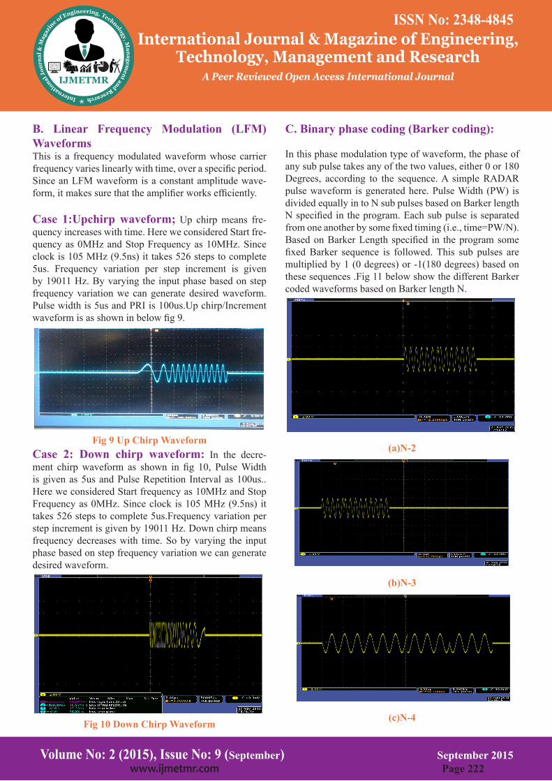
B. Linear Frequency Modulation (LFM) WaveformsThis is a frequency modulated waveform whose carrier frequency varies linearly with time, over a specific period. Since an LFM waveform is a constant amplitude wave-form, it makes sure that the amplifier works efficiently.
Case 1:Upchirp waveform; Up chirp means fre-quency increases with time. Here we considered Start fre-quency as 0MHz and Stop Frequency as 10MHz. Since clock is 105 MHz (9.5ns) it takes 526 steps to complete 5us. Frequency variation per step increment is given by 19011 Hz. By varying the input phase based on step frequency variation we can generate desired waveform. Pulse width is 5us and PRI is 100us.Up chirp/Increment waveform is as shown in below fig 9.
Fig 9 Up Chirp WaveformCase 2: Down chirp waveform: In the decre-ment chirp waveform as shown in fig 10, Pulse Width is given as 5us and Pulse Repetition Interval as 100us.. Here we considered Start frequency as 10MHz and Stop Frequency as 0MHz. Since clock is 105 MHz (9.5ns) it takes 526 steps to complete 5us.Frequency variation per step increment is given by 19011 Hz. Down chirp means frequency decreases with time. So by varying the input phase based on step frequency variation we can generate desired waveform.
Fig 10 Down Chirp Waveform
C. Binary phase coding (Barker coding):
In this phase modulation type of waveform, the phase of any sub pulse takes any of the two values, either 0 or 180 Degrees, according to the sequence. A simple RADAR pulse waveform is generated here. Pulse Width (PW) is divided equally in to N sub pulses based on Barker length N specified in the program. Each sub pulse is separated from one another by some fixed timing (i.e., time=PW/N). Based on Barker Length specified in the program some fixed Barker sequence is followed. This sub pulses are multiplied by 1 (0 degrees) or -1(180 degrees) based on these sequences .Fig 11 below show the different Barker coded waveforms based on Barker length N.
(a)N-2
(b)N-3
(c)N-4
ISSN No: 2348-4845International Journal & Magazine of Engineering,
Technology, Management and ResearchA Peer Reviewed Open Access International Journal
Volume No: 2 (2015), Issue No: 9 (September) September 2015 www.ijmetmr.com Page 223
(d)N=5
(e)N=7
(f)N=11
(g)N=13
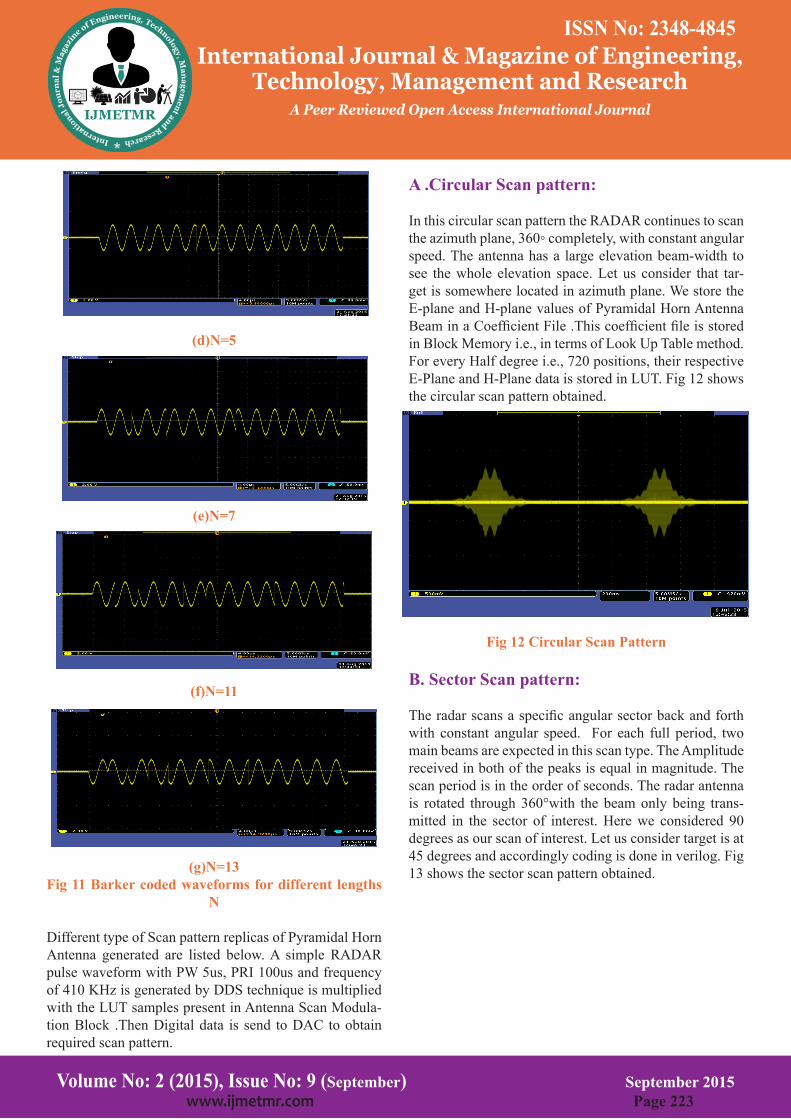
Fig 11 Barker coded waveforms for different lengths N
Different type of Scan pattern replicas of Pyramidal Horn Antenna generated are listed below. A simple RADAR pulse waveform with PW 5us, PRI 100us and frequency of 410 KHz is generated by DDS technique is multiplied with the LUT samples present in Antenna Scan Modula-tion Block .Then Digital data is send to DAC to obtain required scan pattern.
A .Circular Scan pattern:
In this circular scan pattern the RADAR continues to scan the azimuth plane, 360◦ completely, with constant angular speed. The antenna has a large elevation beam-width to see the whole elevation space. Let us consider that tar-get is somewhere located in azimuth plane. We store the E-plane and H-plane values of Pyramidal Horn Antenna Beam in a Coefficient File .This coefficient file is stored in Block Memory i.e., in terms of Look Up Table method. For every Half degree i.e., 720 positions, their respective E-Plane and H-Plane data is stored in LUT. Fig 12 shows the circular scan pattern obtained.
Fig 12 Circular Scan Pattern
B. Sector Scan pattern:
The radar scans a specific angular sector back and forth with constant angular speed. For each full period, two main beams are expected in this scan type. The Amplitude received in both of the peaks is equal in magnitude. The scan period is in the order of seconds. The radar antenna is rotated through 360°with the beam only being trans-mitted in the sector of interest. Here we considered 90 degrees as our scan of interest. Let us consider target is at 45 degrees and accordingly coding is done in verilog. Fig 13 shows the sector scan pattern obtained.
ISSN No: 2348-4845International Journal & Magazine of Engineering,
Technology, Management and ResearchA Peer Reviewed Open Access International Journal
Volume No: 2 (2015), Issue No: 9 (September) September 2015 www.ijmetmr.com Page 222
B. Linear Frequency Modulation (LFM) WaveformsThis is a frequency modulated waveform whose carrier frequency varies linearly with time, over a specific period. Since an LFM waveform is a constant amplitude wave-form, it makes sure that the amplifier works efficiently.
Case 1:Upchirp waveform; Up chirp means fre-quency increases with time. Here we considered Start fre-quency as 0MHz and Stop Frequency as 10MHz. Since clock is 105 MHz (9.5ns) it takes 526 steps to complete 5us. Frequency variation per step increment is given by 19011 Hz. By varying the input phase based on step frequency variation we can generate desired waveform. Pulse width is 5us and PRI is 100us.Up chirp/Increment waveform is as shown in below fig 9.
Fig 9 Up Chirp WaveformCase 2: Down chirp waveform: In the decre-ment chirp waveform as shown in fig 10, Pulse Width is given as 5us and Pulse Repetition Interval as 100us.. Here we considered Start frequency as 10MHz and Stop Frequency as 0MHz. Since clock is 105 MHz (9.5ns) it takes 526 steps to complete 5us.Frequency variation per step increment is given by 19011 Hz. Down chirp means frequency decreases with time. So by varying the input phase based on step frequency variation we can generate desired waveform.
Fig 10 Down Chirp Waveform
C. Binary phase coding (Barker coding):
In this phase modulation type of waveform, the phase of any sub pulse takes any of the two values, either 0 or 180 Degrees, according to the sequence. A simple RADAR pulse waveform is generated here. Pulse Width (PW) is divided equally in to N sub pulses based on Barker length N specified in the program. Each sub pulse is separated from one another by some fixed timing (i.e., time=PW/N). Based on Barker Length specified in the program some fixed Barker sequence is followed. This sub pulses are multiplied by 1 (0 degrees) or -1(180 degrees) based on these sequences .Fig 11 below show the different Barker coded waveforms based on Barker length N.
(a)N-2
(b)N-3
(c)N-4
ISSN No: 2348-4845International Journal & Magazine of Engineering,
Technology, Management and ResearchA Peer Reviewed Open Access International Journal
Volume No: 2 (2015), Issue No: 9 (September) September 2015 www.ijmetmr.com Page 223
(d)N=5
(e)N=7
(f)N=11
(g)N=13
Fig 11 Barker coded waveforms for different lengths N
Different type of Scan pattern replicas of Pyramidal Horn Antenna generated are listed below. A simple RADAR pulse waveform with PW 5us, PRI 100us and frequency of 410 KHz is generated by DDS technique is multiplied with the LUT samples present in Antenna Scan Modula-tion Block .Then Digital data is send to DAC to obtain required scan pattern.
A .Circular Scan pattern:
In this circular scan pattern the RADAR continues to scan the azimuth plane, 360◦ completely, with constant angular speed. The antenna has a large elevation beam-width to see the whole elevation space. Let us consider that tar-get is somewhere located in azimuth plane. We store the E-plane and H-plane values of Pyramidal Horn Antenna Beam in a Coefficient File .This coefficient file is stored in Block Memory i.e., in terms of Look Up Table method. For every Half degree i.e., 720 positions, their respective E-Plane and H-Plane data is stored in LUT. Fig 12 shows the circular scan pattern obtained.
Fig 12 Circular Scan Pattern
B. Sector Scan pattern:
The radar scans a specific angular sector back and forth with constant angular speed. For each full period, two main beams are expected in this scan type. The Amplitude received in both of the peaks is equal in magnitude. The scan period is in the order of seconds. The radar antenna is rotated through 360°with the beam only being trans-mitted in the sector of interest. Here we considered 90 degrees as our scan of interest. Let us consider target is at 45 degrees and accordingly coding is done in verilog. Fig 13 shows the sector scan pattern obtained.
ISSN No: 2348-4845International Journal & Magazine of Engineering,
Technology, Management and ResearchA Peer Reviewed Open Access International Journal
Volume No: 2 (2015), Issue No: 9 (September) September 2015 www.ijmetmr.com Page 224
Fig 13 Sector scan pattern
C. Raster Scan pattern:
The two scan types described above search in only azi-muth, but raster scan searches both in azimuth and eleva-tion. The radar scans a specific angular sector in azimuth and then increases its elevation after finishing the sector. It can have several bars in the elevation. The full period is constant. In each full period, for each bar of the ras-ter scan, a main beam is intercepted. Here we considered sector azimuth angle as 90 degrees and sector elevation angle as 90 degrees. Fig 14 shows the raster scan pattern obtained.
Fig 14 Raster scan pattern
D. Conical Scan Pattern:
This scan type is very important because it is easier to steer the antenna properly to point at a target. It signals that the radar is trying to lock-on to the platform.
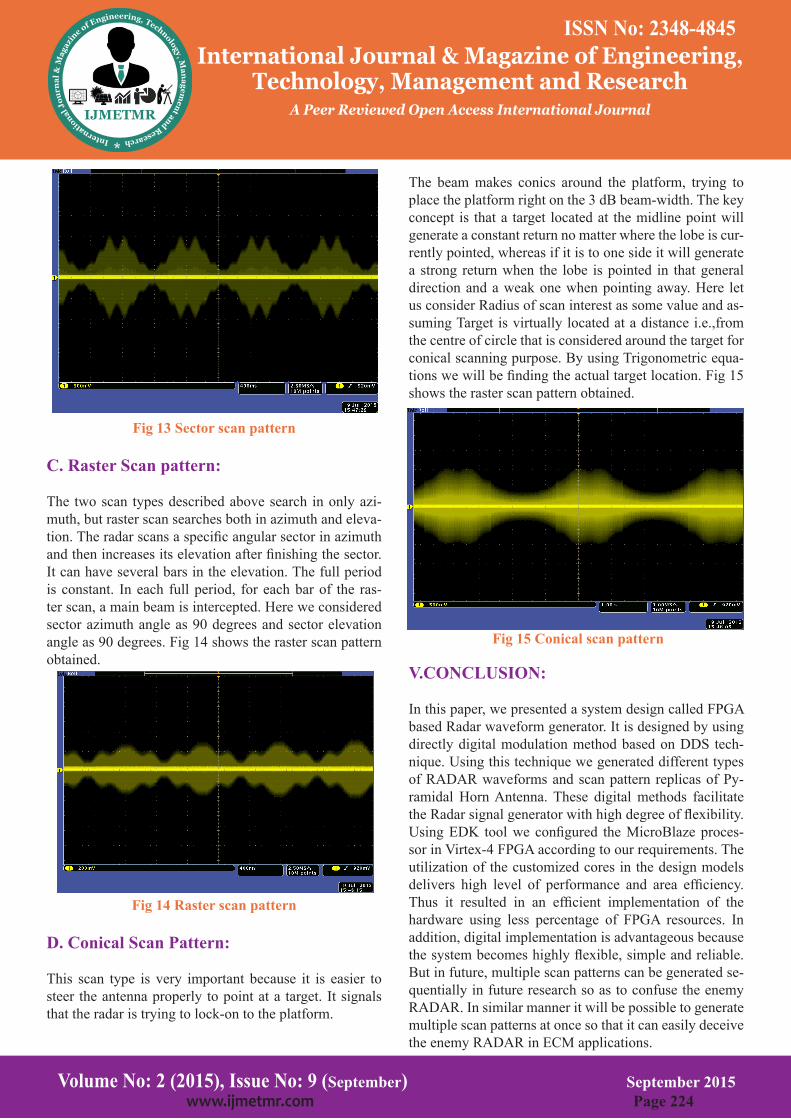
The beam makes conics around the platform, trying to place the platform right on the 3 dB beam-width. The key concept is that a target located at the midline point will generate a constant return no matter where the lobe is cur-rently pointed, whereas if it is to one side it will generate a strong return when the lobe is pointed in that general direction and a weak one when pointing away. Here let us consider Radius of scan interest as some value and as-suming Target is virtually located at a distance i.e.,from the centre of circle that is considered around the target for conical scanning purpose. By using Trigonometric equa-tions we will be finding the actual target location. Fig 15 shows the raster scan pattern obtained.
Fig 15 Conical scan pattern
V.CONCLUSION:
In this paper, we presented a system design called FPGA based Radar waveform generator. It is designed by using directly digital modulation method based on DDS tech-nique. Using this technique we generated different types of RADAR waveforms and scan pattern replicas of Py-ramidal Horn Antenna. These digital methods facilitate the Radar signal generator with high degree of flexibility. Using EDK tool we configured the MicroBlaze proces-sor in Virtex-4 FPGA according to our requirements. The utilization of the customized cores in the design models delivers high level of performance and area efficiency. Thus it resulted in an efficient implementation of the hardware using less percentage of FPGA resources. In addition, digital implementation is advantageous because the system becomes highly flexible, simple and reliable.But in future, multiple scan patterns can be generated se-quentially in future research so as to confuse the enemy RADAR. In similar manner it will be possible to generate multiple scan patterns at once so that it can easily deceive the enemy RADAR in ECM applications.

ISSN No: 2348-4845International Journal & Magazine of Engineering,
Technology, Management and ResearchA Peer Reviewed Open Access International Journal
Volume No: 2 (2015), Issue No: 9 (September) September 2015 www.ijmetmr.com Page 225
REFERENCES:
[1]Sanjay M Trivedi, B. S. Raman, Pinal Engineer and Dr. Mihir Shah, “Field Programmable Gate Array Based Control Signal Generator For Pulsed Radar”, International Journal of Embedded Systems and Applications (IJESA) Vol.2, No.3, September 2012, pp 37-46.
[2]C.Thippeswamy, J.Chinna Babu, K.Padmapriya, “Em-ulator for FPGA based RADAR signal processing”, Inter-national Journal of Engineering and Advanced Technol-ogy (IJEAT) Vol.2, No.1, October 2012, pp 275-278.
[3]A .Nagajyothi, K. Raja Rajeswari, “Graphical User Interface based Signal Generator for Radar/Sonar Pulse Compression Codes”, International Journal of Computer Applications Vol.82, No.16, November 2013, pp 15-19.
[4]Zheng Shenghua; Xu Dazhuan; Jin Xueming; Zhang Shishan; Zhang Hongrong, “An arbitrary waveform gen-erator for SAR test-bench application,” IEEE proceed-ings of Asia-Pacific Microwave Conference, Dec. 2005, pp 4-7.
[5]Wenfeng Dong; Quan Liu; Shirui Peng; Haihong Li, “Design and realization of arbitrary radar waveform gen-erator based on DDS and SOPC technology,” IEEE pro-ceedings of 9th International Conference on Electronic Measurement & Instruments, Aug. 2009, pp 16-19.
[6]Taniza.R, Jadia.K, Raju.G.S.N, Chandramohan, M., “High density FPGA based waveform generation for radars,” in Radar Conference, IEEE May 2010, pp 310-314.
[7]C. Z. Gu, S. Qiao, J. T. Huangfu and L. X. Ran, “DDS Based Radar Signal Generator for Microwave Remote Sensing”, Progress In Electromagnetics Research Sym-posium proceedings, March 24-28, 2008, pp 90-93 .
[8]B.Suresh, M.V.Srikanth, “Radar Waveform Genera-tor based on DDS”, International Journal of Advanced Research in Computer and Communication Engineering Vol. 2, No.9, September 2013,pp 3501-3506.
[9]Shinriki.M, Takase.H, Susaki.H “Pulse compression for a simple pulse,” in IEEE Transactions on Aerospace and Electronic Systems, vol.44, no.4, Oct. 2008, pp 1623-1629.
[10]Merrill I. Skolnik, “Introduction to RADAR sys-tems” Tata McGraw-Hill Education, 01-May-2001, pp 313-370.
[11]Orduyilmaz.A,Kara.G,Serin.M,Yildirim.A, Gurbuz.A.C, Efe.M, “Real-time pulse compression radar wave-form generation and digital matched filtering,” in Radar Conference (RadarCon), IEEE, 10-15 May 2015, pp 0426-0431.
[12]Yong-Hee Kim,Kyu-Ha Song,Jin-Woo Han, Hy-oung-Nam Kim “Radar scan pattern analysis for reduc-tion of false identification in electronic warfare support systems,” in Radar, Sonar & Navigation, IET , vol.8, no.7, Aug. 2014, pp 719-728.
[13]Constantine A. Balanis, “Antenna Theory: Analysis and Design”, Wiley-Interscience, 2005, pp 651-721.
[14]Jigang Liu; Jian Liu, “Spectrum characteristic analy-sis of DDS-based RF digital modulation,” in TENCON 2001. Proceedings of IEEE Region 10th International Conference on Electrical and Electronic Technology, vol.2, 2001, pp 588-591.
[15]BajwaI.S, Chaudhary.M.A, “A Language Engineering System for Graphical User Interface Design (LESGUID): A Rule based Approach,” in Information and Communi-cation Technologies, vol.2, 2006, pp.3582-3586.
[16]MicroBlaze softcore processor User Guide.
[17]Embedded Development Kit tool User Guide.
[18]XtremeDSP Development Kit-IV User Guide..