Embed Size (px)
Citation preview
1
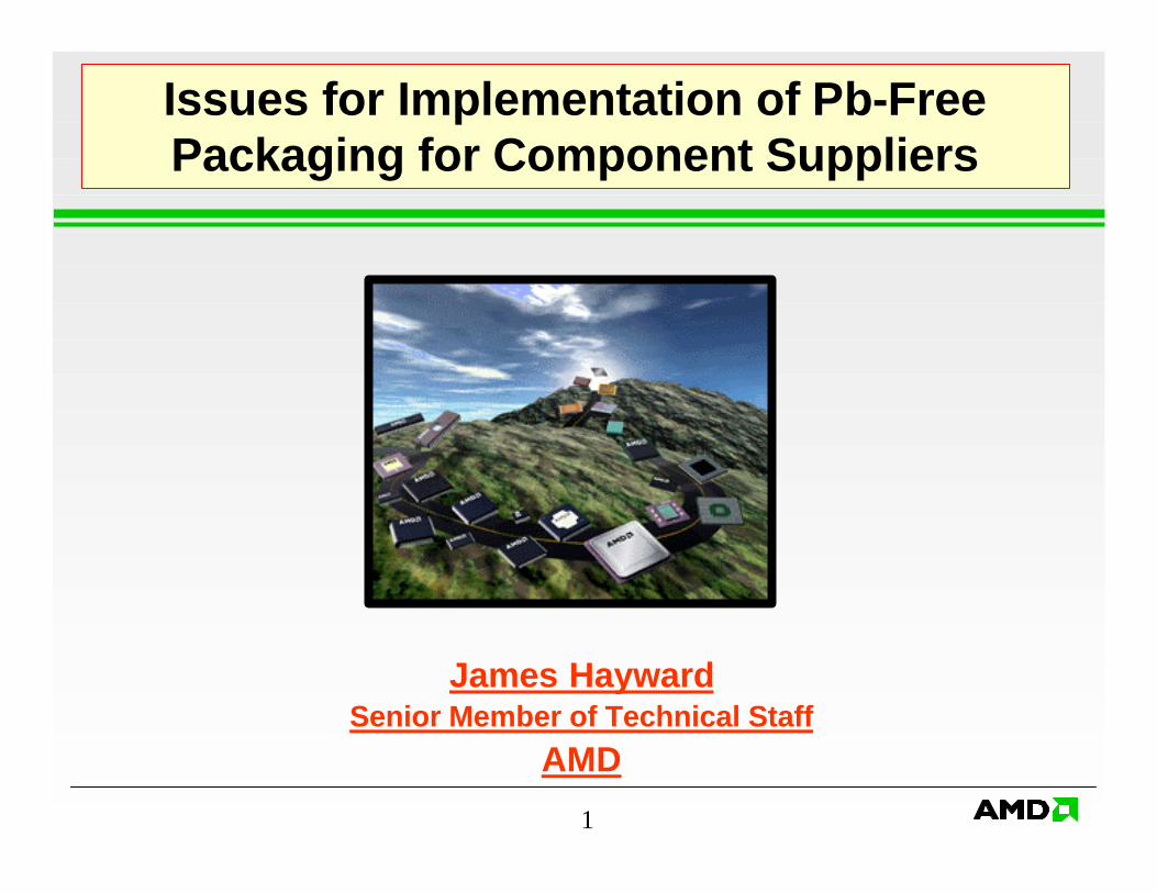
Issues for Implementation of Pb-Free Packaging for Component Suppliers
James HaywardSenior Member of Technical Staff
AMD
James Hayward2
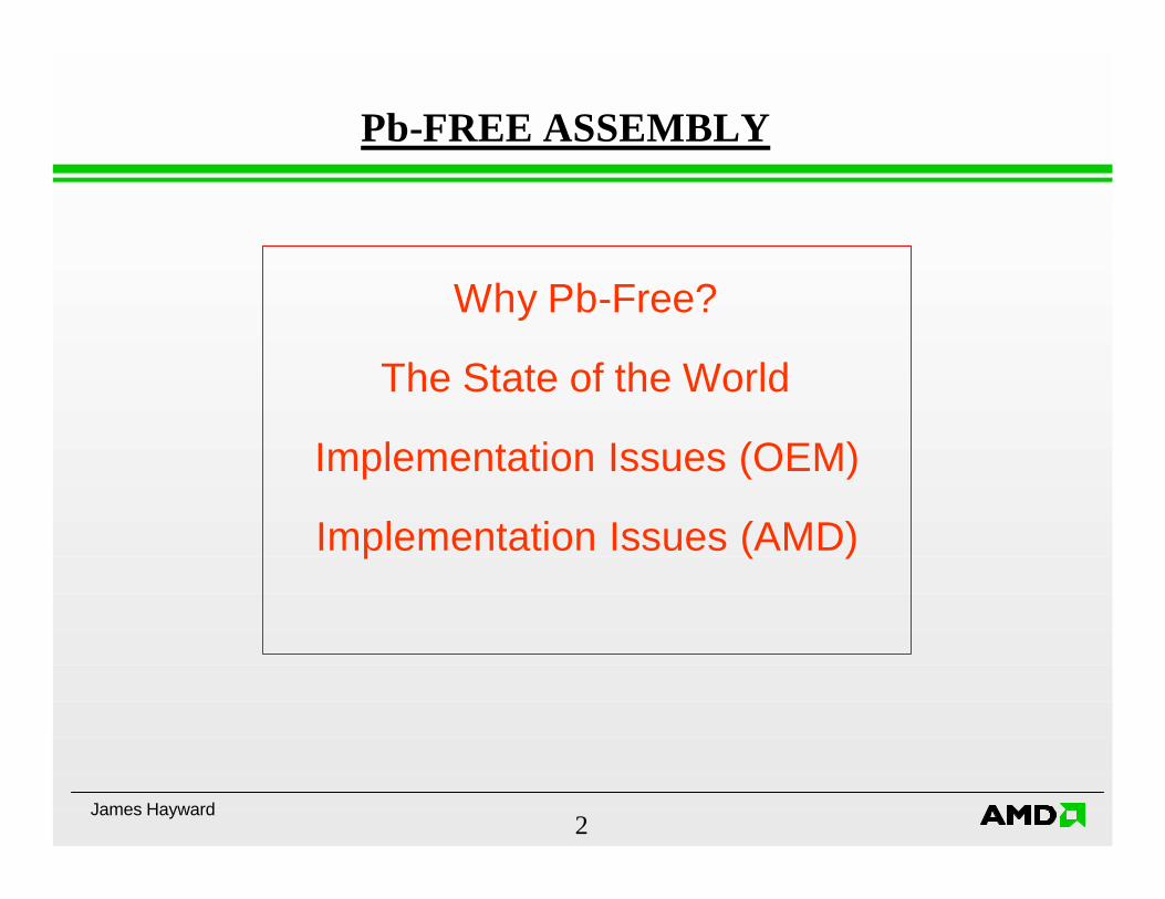
Why Pb-Free?
The State of the World
Implementation Issues (OEM)
Implementation Issues (AMD)
Pb-FREE ASSEMBLY

James Hayward3
l Elimination of lead (Pb) in electronic productsn Lead is already banned in most non-electronic applications
n Concern about accumulation of electronic scrap in landfills
n Electronic waste is claimed to be a growing proportion of landfill solid waste
n Potential leaching of lead into ground water sources (not yet demonstrated to occur in actuality)
n Landfills are being banned in many countries entirely
THE ISSUE
James Hayward4
l Because our customers are interestedn Potential legislative pressure on customers to force the elimination of
lead explicitly (primarily from Europe)
n Marketing pressures on customers to force the elimination of lead (primarily from Japan)
l There is no technical reason why we would do this.n Incompatible with standard eutectic Sn/Pb solder processes
n Parallel manufacturing processes only justified by customer demand
WHY ARE COMPONENT SUPPLIERS INTERESTED

James Hayward5
The State of the World

James Hayward6
l NO existing legislation banning lead explicitly from electronicsANYWHERE
n 1991 US ban exempted electronic equipment
n 1998 proposal in Denmark exempted electronic equipment (proposaldisallowed by EU)
n 1998 Japanese law on Recycling of Household Appliances did not include material bans
n Proposed EU legislation has not yet been passed by European Parliament (despite popular misconception)
LEGISLATIVE ACTIVITY

James Hayward7
l PROPOSED European Union (EU) Directive on Waste in Electrical and Electronic Equipment (WEEE)
n 1st draft (May 1998) incorporating takeback & recycling requirements
n 2nd draft (Oct 1998) added material bans (including lead) with 2004 deadline.
n 3rd draft (July 1999) added exemptions to material bans
n Objections submitted to Directorate General XI by AEA, EIA, PCIF, ORGALIME & others
n Action blocked by “interservice consultation”
n 4th draft (May 2000) pushes material bans to 2008 (submitted to European Parliament in October)
LEGISLATIVE ACTIVITY

James Hayward8
l “GREEN” manufacturing for electronic product salesn “Pb-free” products introduced by Panasonic, Toshiba, Nortel & others
n Focus of “green” products is consumer electronics (audio, video, portable computers, phones)
n Other Japanese companies have announced plans for “lead-free” products
n Products to date use primarily leadframe packages (few BGAs)
n Use Pb-free assembly processes, but not necessarily Pb-free components
n Small volumes: manufacturability, reliability, and yield data not available
n Matsushita announced a program to produce Pb-free ICs (leadframe only)
n Many subsequent announcements of plans
MARKET ACTIVITY

James Hayward9
MARKET ACTIVITY
Panasonic MJ-30 Mini-disk Player
Nortel Meridian Phone Board

James Hayward10
l If Driven by Legislation or Regulation:n Ban will be universal for legislative area for all products (e.g., if EU
passes a Pb ban, then all products produced or sold in Europe must be Pb-free unless exempted)
n “Pb-free” will be a defined condition
l If Driven by Market Forces:n Rationale is marketability; not a technical issuen Ban is product-type and market-area specific; NOT universaln “Pb-free” is a marketing term; not otherwise defined
IMPLICATIONS OF Pb-BAN FORCES

James Hayward11
INDUSTRY RESPONSE TO PROPOSED Pb BANS
OEM SUPPLIER
REQUIREMENTS
l OEMs developing processes independently of each other
l Requirements not discussed with suppliers
l Little concern to date about availability of components (consortial activity beginning in late 1999)
l “Suppliers have always managed before, so why won’t they this time”
l It is an engineering problem. There is no single, correct answer.
James Hayward12
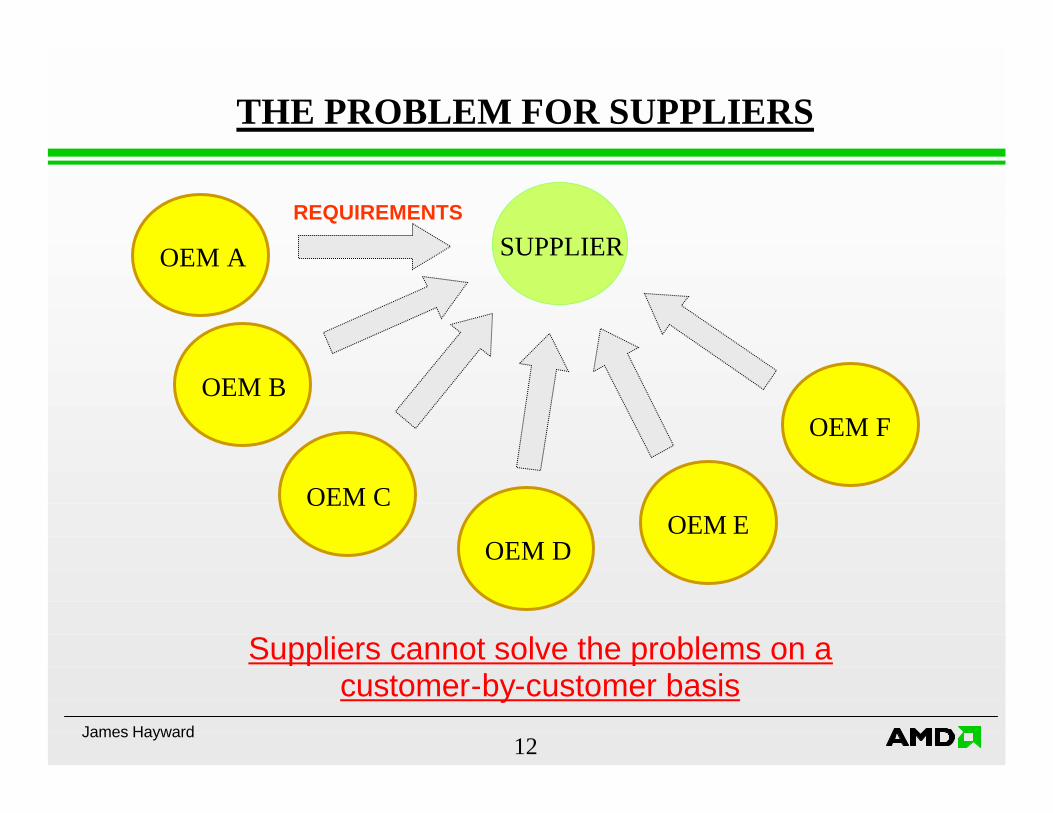
THE PROBLEM FOR SUPPLIERS
OEM A SUPPLIERREQUIREMENTS
OEM B
OEM C
OEM DOEM E
OEM F
Suppliers cannot solve the problems on a customer-by-customer basis
James Hayward13
Implementation Issues (OEMs)

James Hayward14
l What replacements?n Solder paste alloy choice
– Sn/Ag, SnCu, Sn/Bi, many othersn Processing capability
– Solder pastes (availability)– Flux (compatible with higher temperature solder
process)– Screenability – Plating (board finishes)
n Processing temperatures– Furnace profiles– Furnace UPH– Adaptation to existing inline assembly equipment
n Availability of components
Pb BAN ISSUES (OEM)

James Hayward15
Pb-FREE SOLDER REQUIREMENTS
NCMS SOLDER SELECTION CRITERIA
Property Definition Limits
LiquidusTemperature
Temperature at which solder alloy is completelymolten.
< 225°C
Pasty Range Temperature difference between solidus andliquidus temperatures. Represents the temperaturerange where the alloy is part solid and part liquid.
< 30°C
Wettability A wetting balance test assesses the force resultingwhen a copper wire is wetted by molten solder. Alarge force indicates a good wetting, as does a shorttime to attain a wetting force of zero, and a shorttime to attain the two-thirds of the maximumwetting force.
Fmax > 300 µNt0 < 0.6 st2/3 < 1 s
Area of Coverage Assesses the coverage of the solder on Cu after atypical DIP test.
> 85%
Drossing Assesses the amount of oxide formed in air on thesurface of molten solder after a fixed time atsoldering temperature.
Qualitative scale
ThermomechanicalFatigue (TMF-1)
Cycles-to-failure for a given percent failed basedon a specific solder joint/board configuration, ascompared to the eutectic Sn/Pb.
> 75%
Coeff. of ThermalExpansion (CTE)
Differences in thermal expansion behavior betweenalloys might create differences in thermal stresses.
< 29 ppm/°C
Creep Stress required at room temperature to cause failurein 10,000 minutes.
> 500 psi
Elongation Total percent elongation of material under uniaxialtension at room temperature.
> 10%
James Hayward16
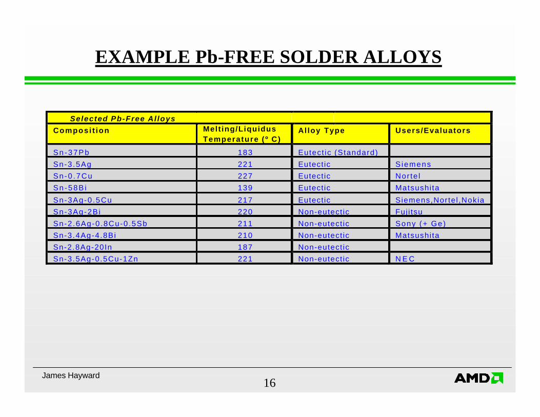
EXAMPLE Pb-FREE SOLDER ALLOYS
Selected Pb-Free Al loys
Composi t ion Melt ing/LiquidusTemperature ( º C)
Al loy Type Users/Evaluators
Sn-37Pb 183 Eutect ic (Standard)
Sn-3.5Ag 221 Eutect ic S iemens
Sn-0 .7Cu 227 Eutect ic Nor te l
Sn -58B i 139 Eutect ic Matsushi ta
Sn-3Ag-0 .5Cu 217 Eutect ic Siemens,Norte l ,Nokia
Sn-3Ag-2Bi 220 Non-eutect ic Fuj i tsu
Sn-2.6Ag-0.8Cu-0.5Sb 211 Non-eutect ic Sony (+ Ge)
Sn-3.4Ag-4.8Bi 210 Non-eutect ic Matsushi ta
Sn-2.8Ag-20In 187 Non-eutect ic
Sn-3.5Ag-0.5Cu-1Zn 221 Non-eutect ic N E C
James Hayward17
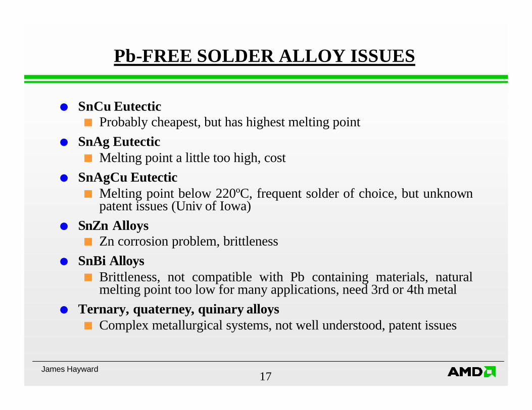
Pb-FREE SOLDER ALLOY ISSUES
l SnCu Eutecticn Probably cheapest, but has highest melting point
l SnAg Eutecticn Melting point a little too high, cost
l SnAgCu Eutecticn Melting point below 220ºC, frequent solder of choice, but unknown
patent issues (Univ of Iowa)l SnZn Alloys
n Zn corrosion problem, brittlenessl SnBi Alloys
n Brittleness, not compatible with Pb containing materials, natural melting point too low for many applications, need 3rd or 4th metal
l Ternary, quaterney, quinary alloysn Complex metallurgical systems, not well understood, patent issues
James Hayward18
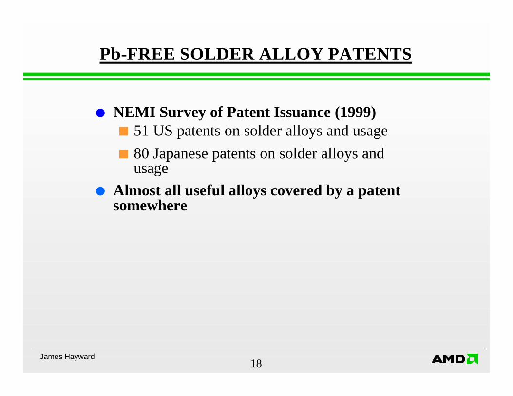
Pb-FREE SOLDER ALLOY PATENTS
l NEMI Survey of Patent Issuance (1999)n 51 US patents on solder alloys and usagen 80 Japanese patents on solder alloys and
usagel Almost all useful alloys covered by a patent
somewhere
James Hayward19
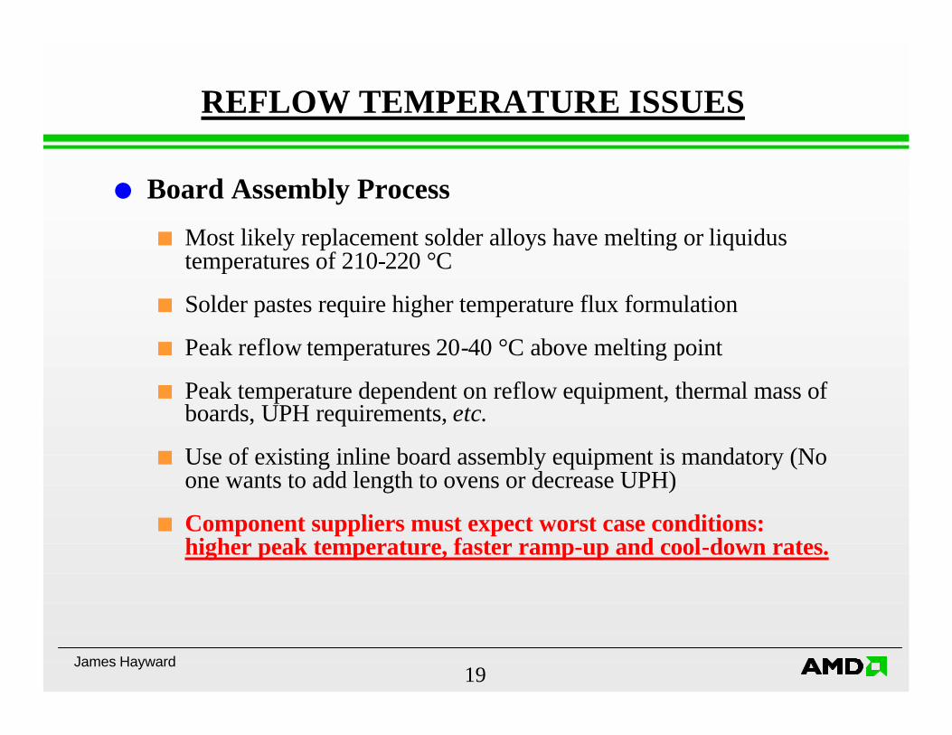
l Board Assembly Process
n Most likely replacement solder alloys have melting or liquidustemperatures of 210-220 °C
n Solder pastes require higher temperature flux formulation
n Peak reflow temperatures 20-40 °C above melting point
n Peak temperature dependent on reflow equipment, thermal mass of boards, UPH requirements, etc.
n Use of existing inline board assembly equipment is mandatory (Noone wants to add length to ovens or decrease UPH)
n Component suppliers must expect worst case conditions: higher peak temperature, faster ramp-up and cool-down rates.
REFLOW TEMPERATURE ISSUES

James Hayward20
Implementation Issues
(Suppliers)
James Hayward21
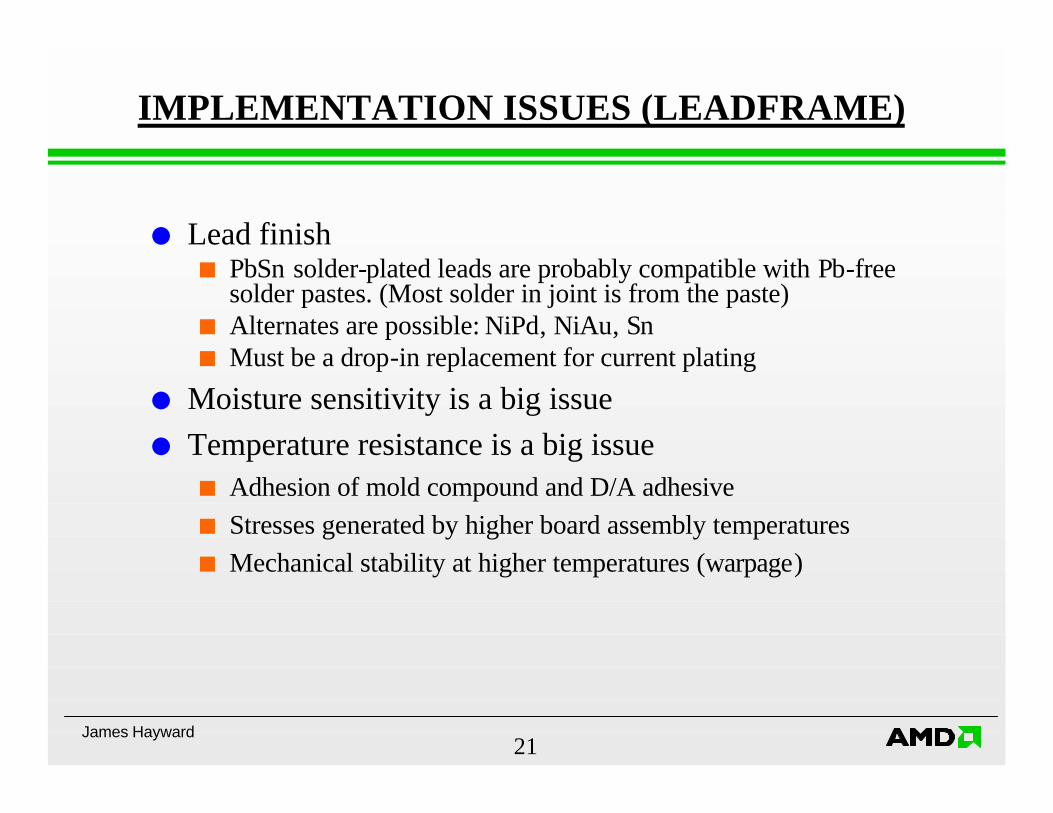
IMPLEMENTATION ISSUES (LEADFRAME)
l Lead finishn PbSn solder-plated leads are probably compatible with Pb-free
solder pastes. (Most solder in joint is from the paste)n Alternates are possible: NiPd, NiAu, Snn Must be a drop-in replacement for current plating
l Moisture sensitivity is a big issuel Temperature resistance is a big issue
n Adhesion of mold compound and D/A adhesiven Stresses generated by higher board assembly temperaturesn Mechanical stability at higher temperatures (warpage)
James Hayward22
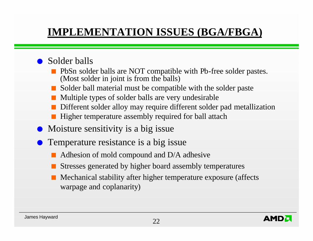
IMPLEMENTATION ISSUES (BGA/FBGA)
l Solder ballsn PbSn solder balls are NOT compatible with Pb-free solder pastes.
(Most solder in joint is from the balls)n Solder ball material must be compatible with the solder pasten Multiple types of solder balls are very undesirablen Different solder alloy may require different solder pad metallizationn Higher temperature assembly required for ball attach
l Moisture sensitivity is a big issuel Temperature resistance is a big issue
n Adhesion of mold compound and D/A adhesiven Stresses generated by higher board assembly temperaturesn Mechanical stability after higher temperature exposure (affects
warpage and coplanarity)

James Hayward23
IMPLEMENTATION ISSUES (FLIPCHIP)
l Solder bumpsn No known alternative to high-Pb/Sn alloy for C4n Eutectic PbSn bumps not an option if higher temperature alloy is used
for board assemblyn Limited choices of alternatives for flipchip bumps to maintain assembly
temperature differential (flipchip connections should have higher melting point than package solder balls)
l Exemptionn IBM objected to proposed WEEE ban for C4n Without legislation flipchip internal to a package may not be an issue.
l Temperature resistance is an issuen Adhesion and stability of underfilln Stresses generated by higher board assembly temperaturesn Mechanical stability at higher temperatures (warpage)n Effect on build-up substrates unknown
James Hayward24
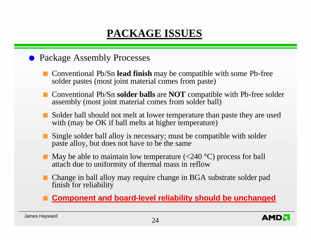
l Package Assembly Processes
n Conventional Pb/Sn lead finish may be compatible with some Pb-free solder pastes (most joint material comes from paste)
n Conventional Pb/Sn solder balls are NOT compatible with Pb-free solder assembly (most joint material comes from solder ball)
n Solder ball should not melt at lower temperature than paste they are used with (may be OK if ball melts at higher temperature)
n Single solder ball alloy is necessary; must be compatible with solder paste alloy, but does not have to be the same
n May be able to maintain low temperature (<240 °C) process for ball attach due to uniformity of thermal mass in reflow
n Change in ball alloy may require change in BGA substrate solder pad finish for reliability
n Component and board-level reliability should be unchanged
PACKAGE ISSUES

James Hayward25
l Package Materials
n Mold compounds for conventional packages (PLCC, PQFP, SO, TSOP) have Tg < 165 °C typically (may be as low as 120-130 °C).
n Die attach materials have Tg of 80-100 °C typically.
n Underfill materials have Tg of 140-160 °C typically.
n Current preconditioning temperatures based on package thermal mass
– PLCC, PQFP: 220 °C peak
– TSOP, FBGA: 235 °C peak
n Questions:– Do materials degrade at 260 °C?– Does adhesion degrade at 260 °C?– Additional plastic deformation at 260 °C?
PACKAGE ISSUES

James Hayward26
l Solder Ball Material
n Pb-free solder alloys are not yet very well characterized
n Typical mechanical properties of favored alloys compared to Sn-37Pb:– Higher Young’s modulus– Higher yield strength– Lower elongation– Creep may not occur
n Morphology and aging characteristics not well understood.
n Intermetallic phase formation not well understoodn What impact will this have on board-level reliability?
– Without good understanding of material behavior cannot do modelling with confidence
PACKAGE ISSUES
James Hayward27
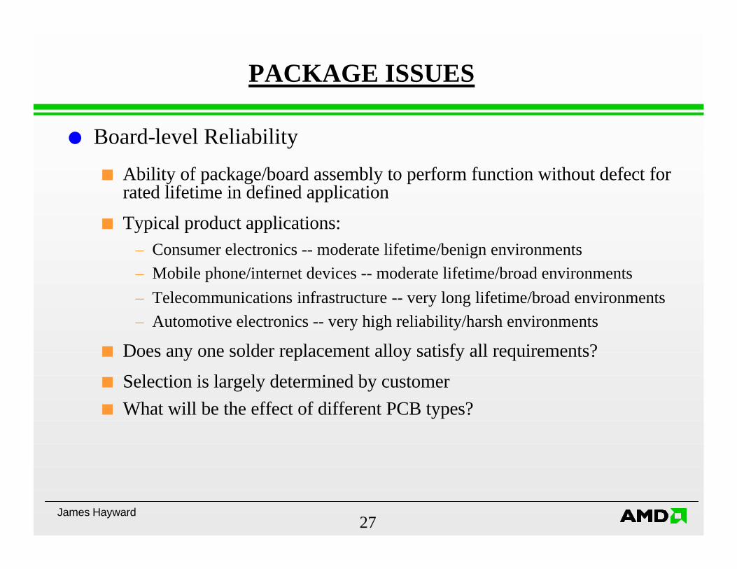
l Board-level Reliability
n Ability of package/board assembly to perform function without defect for rated lifetime in defined application
n Typical product applications:– Consumer electronics -- moderate lifetime/benign environments– Mobile phone/internet devices -- moderate lifetime/broad environments– Telecommunications infrastructure -- very long lifetime/broad environments– Automotive electronics -- very high reliability/harsh environments
n Does any one solder replacement alloy satisfy all requirements?
n Selection is largely determined by customern What will be the effect of different PCB types?
PACKAGE ISSUES

James Hayward28
Phase Map Contour Map
Courtesy of Prof. Paul Ho and Mikel Miller (Univ. of Texas/Austin)
}Microvia layers
PACKAGE ISSUES
l High-Density or Micro-via Board Technology
n Studies of Sn-37Pb systems indicate that stress concentration is in the micro-via layers
n What will be the effect of “stiffer” solder ball materials?
James Hayward29
CONCLUSION
THERE ARE MORE QUESTIONS
THAN THERE ARE ANSWERS