Embed Size (px)
Citation preview
FOR ALL PROJECTS INITIATED AFTER FEBRUARY 1, 2011 1st ISSUE
ITEM 1210
Intelligent Transportation System (ITS) Controller Cabinet Assembly
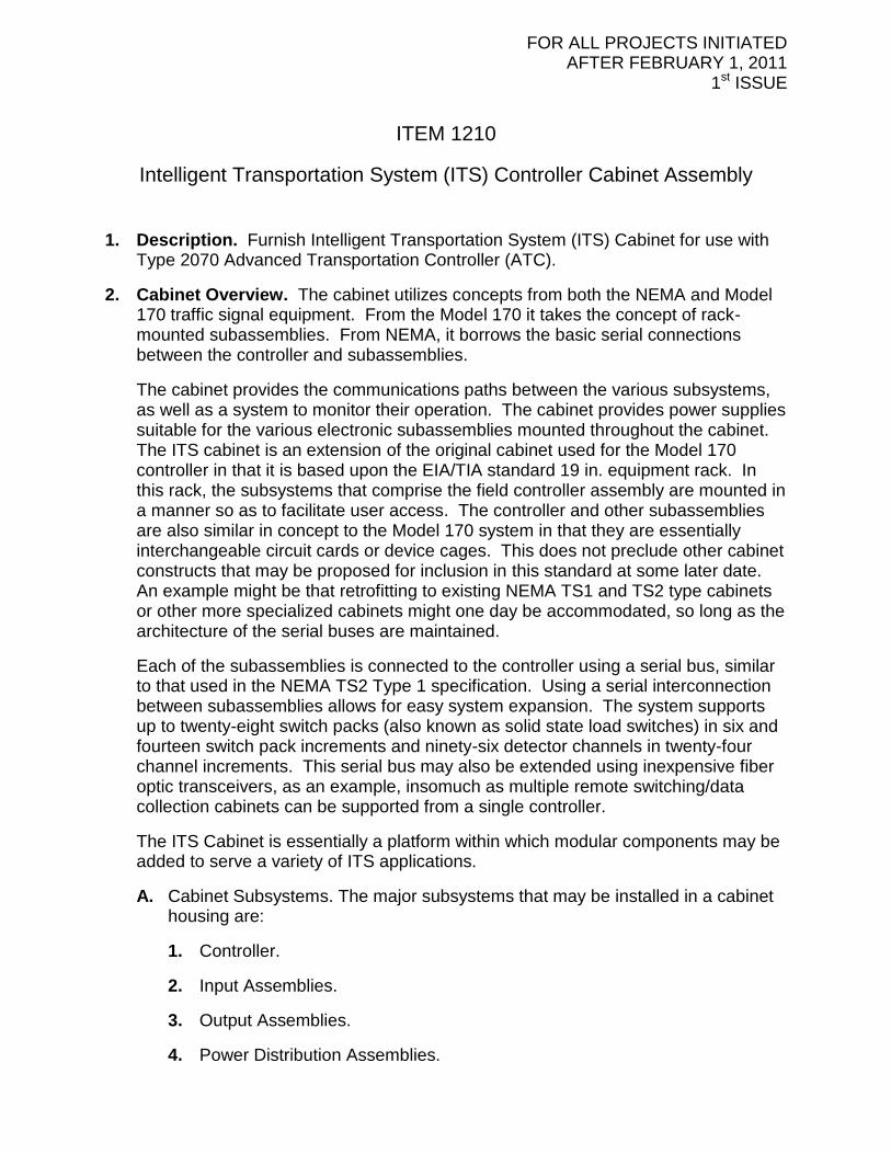
1. Description. Furnish Intelligent Transportation System (ITS) Cabinet for use with Type 2070 Advanced Transportation Controller (ATC).
2. Cabinet Overview. The cabinet utilizes concepts from both the NEMA and Model 170 traffic signal equipment. From the Model 170 it takes the concept of rack-mounted subassemblies. From NEMA, it borrows the basic serial connections between the controller and subassemblies.
The cabinet provides the communications paths between the various subsystems, as well as a system to monitor their operation. The cabinet provides power supplies suitable for the various electronic subassemblies mounted throughout the cabinet. The ITS cabinet is an extension of the original cabinet used for the Model 170 controller in that it is based upon the EIA/TIA standard 19 in. equipment rack. In this rack, the subsystems that comprise the field controller assembly are mounted in a manner so as to facilitate user access. The controller and other subassemblies are also similar in concept to the Model 170 system in that they are essentially interchangeable circuit cards or device cages. This does not preclude other cabinet constructs that may be proposed for inclusion in this standard at some later date. An example might be that retrofitting to existing NEMA TS1 and TS2 type cabinets or other more specialized cabinets might one day be accommodated, so long as the architecture of the serial buses are maintained.
Each of the subassemblies is connected to the controller using a serial bus, similar to that used in the NEMA TS2 Type 1 specification. Using a serial interconnection between subassemblies allows for easy system expansion. The system supports up to twenty-eight switch packs (also known as solid state load switches) in six and fourteen switch pack increments and ninety-six detector channels in twenty-four channel increments. This serial bus may also be extended using inexpensive fiber optic transceivers, as an example, insomuch as multiple remote switching/data collection cabinets can be supported from a single controller.
The ITS Cabinet is essentially a platform within which modular components may be added to serve a variety of ITS applications.
A. Cabinet Subsystems. The major subsystems that may be installed in a cabinet housing are:
1. Controller.
2. Input Assemblies.
3. Output Assemblies.
4. Power Distribution Assemblies.
Item 1210 FOR ALL PROJECTS INITIATED Page -2- AFTER FEBRUARY 1, 2011 1ST ISSUE
2-197
5. Fiber Optic Splice Tray (Optional, not specified herein).
6. Service Panel Assembly.
7. DC Power/Communications Assembly & Extension.
8. RAW/CLEAN AC Power Assembly & Extension.
9. Cabinet Monitoring System.
The cabinet is constructed in a modular manner with power distribution and serial connectors conveniently located throughout the cabinet to facilitate a wide variety of configurations and future expansion. Each of these subassemblies is discussed below. A separate standard describes the controller.
a. Input Assembly. The input assembly provides services for the typical inductive loop detectors currently in use, as well as other more advanced systems that might provide the controller with serial data instead of the typical contact closure. Each assembly accommodates one Serial Interface Unit (SIU) to communicate with the controller. The rack has space for twelve two-channel detector units or six four-channel detector units. The system can address (i.e. the Serial Bus addressing structure supports) up to four of these assemblies.
The detectors in the assembly can communicate to the controller in the form of either a contact closure or use of serial data strings. The back plane of this assembly includes a serial bus to transmit data to and from detectors. This serial data is then transmitted to the controller by Serial Bus 1, which is described below. This allows for the use of “smart” detectors that can pass additional information such as vehicle classification, Automatic Vehicle Identification/Location information, speed information directly to the controller unit. Each slot provides general purpose power and input/output signals and a serial interface.
The input “slots” can also accommodate the standard collection of Model 170 or NEMA TS2 type cards, including preemption devices, and isolation modules, using the contact closure interface.
b. Output Assembly 6 and 14 Pack. The output assembly handles the switching of 120 VAC power to the signal heads. There are two versions of this assembly, one to accommodate six switch packs and one for fourteen switch packs. It also has an SIU and an Auxiliary Monitor Unit (AMU). The AMU is described in more detail in a following section. The output assembly includes provisions for managing cabinet flash with Flash Transfer Relays and flash configuration jumpers.
To support the AMU function of current monitoring, the output assembly includes current monitoring transformers for each switch pack. These current monitor transformers enable the detection of a “no-load” condition on a signal without having to wait for the signal to cycle.

Item 1210 FOR ALL PROJECTS INITIATED Page -3- AFTER FEBRUARY 1, 2011 1ST ISSUE
3-197
The system can address (i.e. the Serial Bus addressing structure supports) ten combinations of six switch and fourteen switch assemblies. For a maximum configuration the system can address two fourteen switch pack modules for a total of twenty-eight switch packs or physical channels, plus four virtual channels for a total of thirty-two logical channels.
The field wires can also be connected to the back of this unit using plug-in type connectors. The field wires are terminated in these connectors, which are then be plugged into the back of the Assembly. This facilitates the change out of the assembly or the whole controller and housing assembly.
c. Power Distribution Assembly (PDA 5 IP or EP). The PDA provides protected power distribution to the various devices and subassemblies within the cabinet. This assembly also houses Emergency Flasher Units, control relays, signal power contactor, and the Cabinet Monitor Unit (CMU).
The PDA IP houses two low voltage DC power supplies. One provides power to 24 VDC devices, the other to 12 VDC devices. Each of these power supplies is packaged as a slide-out subassembly. The PDA EP provides protected power distribution to the various devices and subassemblies within the cabinet. This assembly also houses Emergency Flasher Units, control relays, signal power contactor, and the Cabinet Monitor Unit (CMU).
The PDA EP requires an external rack mounted low voltage DC power supply for power to 24 VDC devices such as detectors and switchpacks. Dual Rack Cabinets may require an additional 12 VDC Supply if more than 3 Input Assemblies are required. Each of these power supplies is packaged as a rack mount assembly.
PDA 5 EP with Rack Mount Power Supplies
PDA 5 IP with internal Power Supplies
Figure 1
PDA 5 IP and EP
Item 1210 FOR ALL PROJECTS INITIATED Page -4- AFTER FEBRUARY 1, 2011 1ST ISSUE
4-197
Modular Buses. The modular buses are assemblies that are mounted on the rack rails in the back of the cabinet and provide a pluggable interconnection of the Assembly units to the controller unit and power. These assemblies control and protect the wiring between these key subsystems, provides additional shielding from electromagnetic interference. Their biggest benefit is to simplify cabinet assembly.
The cabinet may have any combination of these bus units depending upon the particular application. For example, a cabinet designed as a communications hub may only have a Modular Power Assembly unit. A small pole mounted cabinet (proposed but not included in this standard) may not have any of them and those installed in Cabinet Housing 2 would not use the extensions.
(1) Raw/Clean AC Power Assemblies. The Raw/Clean AC Power Assembly attaches to the right rear rack rail. This assembly is internally wired to provide 120 VAC “clean power” to the controller, output assemblies and auxiliary devices needed within the Cabinet, as well as Signal and flasher power from the PDA is distributed by P1 and S1 to S4 to the Output Assemblies. The Raw/Clean Bus Assemblies are available in two configurations, a four socket and a two socket version. With the advent of the 14 Pack Output Assembly the two socket version provides adequate power distribution for most applications and with the additional clean power sockets it will eliminate the need for the extension. Extension Bus Assemblies are provided for additional clean power service when needed and room permits. A AC Clean Modular Assembly is used to power the left hand rack in Housing 3. This assembly is primarily meant for those cabinets without output assemblies or for use in the dual rack system.
(2) DC Power /Communications Assembly and Extension. This modular bus assembly provides 12 VDC and 24 VDC power to cabinet .assemblies. It also houses the wiring for the serial buses 1 and 2 communications between the SIUs, CMUs, AMUs and the ATC Controller Unit. The Extension provides additional DC Power when needed.
d. Cabinet Monitoring System. The cabinet monitoring system provides a fail-safe mechanism for the entire collection of subassemblies. The system for the ATC is a departure from its predecessors in that it has been split into sub components, the Cabinet Monitor Unit (CMU) and the Auxiliary Monitor Unit (AMU). The adjacent diagram illustrates the architecture.
The real power of this architecture is that it allows the user a much greater degree of flexibility in cabinet configurations than previously possible. This diagram shows the control system for a single intersection. The use of serial communications to the CMU is a very
Item 1210 FOR ALL PROJECTS INITIATED Page -5- AFTER FEBRUARY 1, 2011 1ST ISSUE
5-197
powerful concept. Serial communications to multiple CMUs allow for the response to a conflict at a single intersection and not impact other intersections/ramps/etc. operated by the same controller. Therefore, one intersection could go to flash independently of the others, provided that each cabinet (or each independent output assembly) has a PDA within which a CMU is installed.
(1) Cabinet Monitor Unit (CMU). The CMU is housed in the PDA. There should only be one of these installed in each cabinet, or each grouping of output assemblies. It is the main processor unit of the cabinet monitoring system. It monitors main cabinet functions, such as the condition of cabinet power, door status, and status of the flasher. It communicates with the AMUs located in the output assemblies and compares requested actions (from the controller) with the actual cabinet operation (switch pack outputs) to detect errors, conflicts, and other anomalies. It can then direct the cabinet to a flashing or fail-safe condition.
The exception here is the Cabinet Housing 3, which could contain two separate groupings of input, output and power distribution assemblies for two separate intersections all controlled by a single controller.
The configuration and operational characteristics of the CMU is determined by software. This programming may be customized to user needs and desires. There is also a specific reporting format, in order to address the minimum mandatory functionality of this unit. The minimum functionality is at least that provided by the NEMA TS2 Malfunction Monitoring Unit.
To allow full programmability of the CMU, without a massive number of physical jumpers, the Model 210 and NEMA diode based conflict programming board is replaced by a serial memory key. This serial memory key contains all information to configure the monitoring system as well as other cabinet configuration information.
The CMU might carry an address so that multiple CMUs could be used to provide multiple intersection control assemblies controlled by a single controller. The CMU addressing is accomplished through address jumper programming on the rear of the PDA. A maximum of four CMUs are allowed.
(2) Auxiliary Monitor Unit (AMU). The AMU is housed in each output assembly. This unit does the basic monitoring of the output of the switch packs and reports their status to the CMU. It is essentially a device that monitors the output voltage and current of each circuit of each switch pack. This module communicates to the CMU via Serial Bus 3. Having this unit as a separate module from the CMU allows greater modularity of the cabinet. The cabinet can contain
Item 1210 FOR ALL PROJECTS INITIATED Page -6- AFTER FEBRUARY 1, 2011 1ST ISSUE
6-197
any grouping of between one and four output assemblies. However, the grouping of output assemblies and associated CMU connected via a single Serial Bus 3 would remain as an associated grouping and not be split to different cabinets.
(3) Serial Memory Key. This key is essentially a non-volatile computer memory device. There are two of these devices in the system, one in the controller and one in the CMU. It contains all the specific information to define unit operations and malfunctions. In general, the key in the CMU replaces the Model 210 and NEMA Conflict Monitor Programming Card, plus any information previously programmed into those units. The CMU serial memory key does not contain the controller operating and application software. Start-up processes within the cabinet allow the CMU, and the controller, to verify a compatible configuration before starting normal operation.
e. Cabinet Communications Systems. The controller communicates with the various cabinet subassemblies via a serial bus arrangement. There are three separate serial buses employed. These buses are similar to those used in the NEMA TS2 specification and communicate using a Synchronous Data Link Control (SDLC) protocol. The Cabinet Block Diagram illustrates how this system is configured. The electrical characteristics of this communications circuit are defined by EIA/TIA 485 specifications.
(1) Serial Interface Unit (SIU). The SIU functions as the cabinet communications and control unit. The SIU communicates with the ATC Controller Unit through Serial Bus 1 and Serial Bus 2 via the Modular Bus Assembly. In the case where the input and/or output assembly is mounted remotely, communications would be over a data grade interconnect cable. This cable might be a fiber optic cable because of its high noise immunity and reliability.
A SIU is needed for each input assembly and each output assembly connected to the ATC Controller Unit.
(2) Serial Bus 1. This bus communicates real time information required to operate the system. It handles the highest priority, time sensitive data exchange between the SIUs in the input and output assemblies, controller unit and the CMU. An example would be the commands to the switch packs to change signal color or data from detection inputs. Serial Bus 1 is designed for a communications rate of 614,400 bits per second.
(3) Serial Bus 2. This bus communicates less time critical information between the SIUs in the input and output assemblies, and the controller unit. An example would be servicing requests for general program information as might be requested from a central computer
Item 1210 FOR ALL PROJECTS INITIATED Page -7- AFTER FEBRUARY 1, 2011 1ST ISSUE
7-197
system. Serial Bus 2 is designed for an allowable communications rate of 614,400 bits per second.
(4) Serial Bus 3. This bus is dedicated to communications between the AMUs and the CMU. It is used to allow the CMU to monitor the various voltages, operating conditions, and currents in the output assemblies to determine actual switch pack conditions. Serial Bus 3 has an operating communications rate of 153,600 bits per second.
B. Standard Cabinet Assemblies. There are three different cabinet assemblies, which consist of a specific collection of the subassemblies described above. Each of these assemblies is installed in a cabinet that is designed for a particular group of applications and is sized to hold the equipment required. The cabinets have doors both on the front and the back. The equipment is mounted on a standard EIA 19 in. rack that is fitted inside each cabinet.
Each cabinet includes at least the following common features:
Enclosure Gasketing
Doors Police Panel
Latches/Locks Ventilation and Air Filtration
Hinges and Door Catches Assembly Supports and Mounting
1. Cabinet Housing 1. This Cabinet Housing is very similar to the Type 332 series of cabinet used for the Model 170 Controller system. It is a single rack cabinet with sufficient capacity to operate a full eight-phase traffic signal. Dimensions are width 24.25 in., depth 30.25 in., and height 66.78 in.
2. Cabinet Housing 2. This shorter version of Cabinet Housing 1 is very similar to the Type 336S series of cabinet used for the Model 170 Controller system and is meant for applications that require less space for inputs and outputs. This cabinet might be found at small two through eight-phase traffic signals, ramp meters, data stations and similar less space demanding applications. Dimensions are width 24.25 in., depth 20.25 in., and height 46.25 in.
3. Cabinet Housing 3. This is a large two rack, four door cabinet with bottom details and a bolt pattern similar in size to the NEMA P cabinet. It is meant for installations requiring a lot of equipment. An example application may be a traffic signal controller with a communications hub or a ramp meter, or perhaps additional input/output assemblies. Dimensions are width 44.50 in., depth 26.00 in., height 66.38 in.
3. General ITS Cabinet Requirements.
A. General. All furnished equipment must be new and unused. Vacuum or gaseous tubes and electro-mechanical devices (unless specifically called out) will not be used.
Item 1210 FOR ALL PROJECTS INITIATED Page -8- AFTER FEBRUARY 1, 2011 1ST ISSUE
8-197
1. References. Reference is made to the following documents:
ATC 2070 v01.05, Advanced Transportation Controller (ATC) Standard for the Type 2070 Controller, dated March 29, 2001
2. Interchangeability. Assemblies and their associated devices must be electrically and mechanically interchangeable at both the assembly and device levels:
ASSEMBLIES ASSOCIATED DEVICES
Input Assembly - Model 222, 232 & 224 Sensor Unit
- Model 242 and 252 Isolator Unit - Type 218 Serial Interface Unit (SIU)
Output Assembly - Model 200 Switch Pack Unit
- Model 205 Transfer Relay Unit - Model 214 Auxiliary Monitor Unit - Type 218 SIU Unit
PDA ITS - Model 204 Flasher Units
- Model 212 Cabinet Monitor Unit - Model 216-12 & 216-24 Power Supply Units
B. Documentation.
1. Manuals. Two copies of Manual Documentation must be supplied for each item purchased up to 200 manuals per order. The manual must be bound in durable covers made of either 65-pound stock paper or clear plastic. The manual must be printed on paper measuring 8-1/2 in. by 11 in., with the exception that schematics, layouts, parts lists and plan details may be on sheets measuring 11 in. by 17 in., with each sheet neatly folded to a size of 8-1/2 in. by 11 in. A minimum of Times New Roman or Arial 10 point font must be used for all manual text, excluding drawings and schematics. Drawing text may use a smaller font size.
a. Cabinet Wiring Diagrams. Two copies of Cabinet Wiring Diagrams must be included in each cabinet. Cabinet Wiring Diagrams must be on non-fading, minimum 22 in. x 34 in., sheets.
b. Manual Contents. Each manual must utilize the following outline, to the extent possible:
(1) Table of Contents
(2) Glossary
(3) Manufacturer Contact Information
(a) Address
Item 1210 FOR ALL PROJECTS INITIATED Page -9- AFTER FEBRUARY 1, 2011 1ST ISSUE
9-197
(b) Telephone Number
(c) Fax Number
(d) General Email Address
(4) General Description
(5) General Characteristics
(6) Installation
(7) Adjustments
(8) Theory of Operation
(a) Systems Description (include block diagram).
(b) Detailed Description of Circuit Operation.
(9) Maintenance
(a) Preventive Maintenance.
(b) Trouble Analysis.
(c) Trouble Shooting Sequence Chart.
(d) Wave Forms.
(e) Voltage Measurements.
(f) Alignment Procedures.
(10) Parts List (include circuit and board designation, part type and class, power rating, component manufacturer, mechanical part manufacturer, data specification sheets for special design components and original manufacturer's part number).
(11) Electrical Interconnection Details & Drawings.
(12) Schematic and Logic Diagram
(13) Assembly Drawings and a pictorial diagram showing physical locations and identification of each component or part.
(14) The date, serial numbers, model numbers and revision numbers of equipment covered by the manuals must be printed on the front cover of the manuals.
c. Manual Pouches. Manuals for the cabinet must be furnished in a weatherproof plastic pouch placed in the cabinet.
Item 1210 FOR ALL PROJECTS INITIATED Page -10- AFTER FEBRUARY 1, 2011 1ST ISSUE
10-197
d. Draft Manual. A preliminary draft of the manual must be submitted, when required, to the AGENCY for approval prior to final printing.
C. Packaging. Each item delivered must be individually packed in its own shipping container. When loose Styrofoam is used for packing the item, the item must be sealed in a plastic bag to prevent direct contact with the Styrofoam.
D. Delivery. Each item delivered for testing must be complete, including manuals, and ready for testing.
E. Metals. All sharp edges and corners must be rounded and free of any burrs.
1. Aluminum. Aluminum sheets must be Type 3003-H14 or Type 5052-H32 ASTM B209 aluminum alloy. Rod, Bar and Extruded must be Type 6061-T6, or equal.
2. Stainless Steel. Stainless Steel sheets must be annealed or one-quarter-hard complying with the ASTM A666 for Type 304, Grades A or B, stainless steel sheet.
3. Cold Rolled Steel. Cold Rolled Steel sheet, rod, bar and extruded must be Type 1018/1020.
a. Plating. All cold roll steel must be plated. All plating must be either cadmium plating meeting the requirements of Federal Specification QQ-P-416C, Type 2 Class l or zinc plating meeting the requirements of ASTM B633-85 Type II SC4.
F. Mechanical Hardware. All bolts, nuts, washers, screws, hinges and hinge pins must be stainless steel unless otherwise specified.
G. Electrical Isolation. Within the circuit of any device, module, or Printed Circuit Board (PCB), electrical isolation must be provided between DC logic ground, equipment ground and the AC- conductor. They must be electrically isolated from each other by 500 Megohms, minimum, when tested at the input terminals with 500 VDC.
H. Daughter Boards. Keyboards and LCD/LED Displays are considered daughter boards. Daughter boards must be mechanically secured with a minimum of four spacers/metal screws. Connectors must be either Flat Cable or PCB Headers. Components are allowed to be mounted under the daughter board.
4. Components.
A. General. All components must be second sourced and be of such design, fabrication, nomenclature or other identification as to be purchased from a wholesale distributor or from the component manufacturer, except as follows:
1. When a component is of such special design that it precludes the purchase of identical components from any wholesale distributor or component manufacturer, one spare duplicate component must be furnished with each 20, or fraction thereof, components used.
Item 1210 FOR ALL PROJECTS INITIATED Page -11- AFTER FEBRUARY 1, 2011 1ST ISSUE
11-197
2. The electronic circuit design must be such that all components of the same generic type, regardless of manufacturer, function equally in accordance with the specifications.
B. Electronic Components.
1. No device to be socket mounted unless specifically called out.
2. No component to be operated above 80% of its maximum rated voltage, current or power ratings. Digital components must not be operated above 3% over their nominal voltage, current or power ratings.
3. Components must have been kept in the original packaging and stored in a proper environment, according to the manufacturers instructions. The design life of all components, operating for twenty-four hours a day and operating in their circuit application, must be ten years or longer.
4. Components must be arranged so they are easily accessible, replaceable and identifiable for testing and maintenance. Where damage by shock or vibration exists, the component must be supported mechanically by a clamp, fastener, retainer, or hold-down bracket.
5. The Manufacturer must submit detailed engineering technical data on all components at the request of the AGENCY. The Manufacturer must certify that the component application meets the requirements of this standard.
C. Capacitors. The DC and AC voltage ratings, as well as the dissipation factor, of a capacitor must exceed the worst-case design parameters of the circuitry by 150%. Capacitor encasements must be resistant to cracking, peeling and discoloration. All capacitors must be insulated and be marked with their capacitance values and working voltages. Electrolytic capacitors must not be used for capacitance values of less than 1.0 microfarad and be marked with polarity.
D. Potentiometers. Potentiometers with ratings from 1 to 2 watts must meet Military Type RV4 requirements. Under 1 Watt potentiometers must be used only for trimmer type function. The potentiometer power rating must be at least 100% greater than the maximum power requirements of the circuit.
E. Resistors. Fixed carbon film, deposited carbon, or composition-insulated resistors must conform to the performance requirements of Military Specifications MIL-R-11F or MIL-R-22684. All resistors must be insulated and be marked with their resistance values. Resistance values must be indicated by the EIA color codes, or stamped value. The value of the resistors must not vary by more than 5% between -37 degrees C and 74 degrees C.
1. Special ventilation or heat sinking must be provided for all 2- watt or greater resistors. They must be insulated from the PCB.
F. Semiconductor Devices.
Item 1210 FOR ALL PROJECTS INITIATED Page -12- AFTER FEBRUARY 1, 2011 1ST ISSUE
12-197
1. All transistors, integrated circuits, and diodes must be a standard type listed by EIA and clearly identifiable.
2. All metal oxide semiconductor components located in a sub-assembly must contain circuitry to protect their inputs and outputs against damage due to high static voltages or electrical fields.
3. Device pin "1" locations must be properly marked on the PCB adjacent to the pin.
G. Transformers and Inductors. All power transformers and inductors must have the manufacturer's name or logo and part number clearly and legibly printed on the case or lamination. All transformers and inductors must have their windings insulated, be protected to exclude moisture, and their leads color coded with an approved EIA color code or identified in a manner to facilitate proper installation.
H. Triacs. Each triac with a designed circuit load of greater than 0.5 Amperes at 120 VAC must be mounted to a heat sink with thermal conductive compound or material, in addition to being mechanically secured.
I. Circuit Breakers. Circuit breakers must be listed by UL or ETL. The trip and frame sizes must be plainly marked (marked on the breaker by the manufacturer), and the ampere rating must be visible from the front of the breaker. Contacts must be silver alloy and enclosed in an arc quenching chamber. Overload tripping must not be influenced by an ambient air temperature range of from -18 degrees C to 50 degrees C. The minimum Interrupting Capacity must be 5,000 Amperes, RMS when the breaker is secondary to a UL approved fuse or primary circuit breaker and both breakers in concert provide the rated capacity. For circuit breakers 80 Amperes and above, the minimum interrupting capacity must be 10,000 Amperes, RMS. Circuit breakers must be the trip-free type with medium trip delay characteristic (Carlingswitch Time Delay Curve #24 or equal).
1. Load Circuit Breaker Auxiliary Internal Switches. The Load Circuit Breakers located on the PDA that are used to control Output Assembly Model 200 Switch Packs must have auxiliary switches. The auxiliary switches must “open” when the load breaker has tripped and the system will transfer the power from the Main Contactor to the Flash or Blank condition.
J. Fuses. All Fuses that are resident in a bayonet style fuse holder must have the fuse size rating labeled on the holder or on the panel adjacent to the holder. Fuses must be easily accessible and removable without use of tools.
K. Switches.
1. Dip. Dual-inline-package, quick snap switches must be rated for a minimum of 30,000 operations per position at 50 milliamperes, 30 VDC. The switch contact resistance must be 100 milliohms maximum at 2 milliamperes, 30 VDC. The contacts must be gold over brass.
Item 1210 FOR ALL PROJECTS INITIATED Page -13- AFTER FEBRUARY 1, 2011 1ST ISSUE
13-197
2. Logic. The switch contacts must be rated for a minimum of 1 Ampere resistive load at 120 VAC and be silver over brass (or equal). The switch must be rated for a minimum of 40,000 operations.
3. Control. The switch contacts must be rated for a minimum of 5 Amperes resistive load at 120 VAC or 28 VDC and be silver over brass (or equal). The switch must be rated for a minimum of 40,000 operations.
4. Power. Ratings must be the same as CONTROL, except the contact rating must be a minimum of ten Amperes at 125 VAC.
L. Terminal Blocks. The terminal blocks must be barrier type, rated at 20 Amperes and 600 VAC RMS minimum. The terminal screws must be 0.3125 in. minimum length nickel plated brass binder head type with screw inserts of the same material. Screw size is called out under the associated file, panel or assembly.
M. Screw Lug and Cam Driven Connectors. Provided the connectors mate, screw lug cam driven devices or crimp pin connectors must be allowable if the interface is part of a harness. For field termination, screw lug and cam driven assemblies are interchangeable for field wiring termination, provided they both accommodate 22-gauge wire on the inputs and 22-gauge wire on the outputs.
N. Wiring, Cabling and Harnesses.
1. Harnesses must be neat, firm and properly bundled with external protection. They must be tie-wrapped and routed to minimize crosstalk and electrical interference. Each harness must be of adequate length to allow any conductor to be connected properly to its associated connector or termination point. Conductors within an encased harness have no color requirements. Printed circuit motherboards are to be used where possible to eliminate or reduce cabinet wiring.
2. Wiring containing AC must be bundled separately or shielded separately from all DC logic voltage control circuits.
3. Wiring must be routed to prevent conductors from being in contact with metal edges. Wiring must be arranged so that any removable assembly may be removed without disturbing conductors not associated with that assembly.
4. All conductors, except those that can be readily traced, must be labeled. Labels attached to each end of the conductor must identify the destination of the other end of the conductor.
5. All conductors must conform to MIL-W-16878E/1 or better and have a minimum of 19 strands of copper. The insulation must be polyvinyl chloride with a minimum thickness of 10 mils or greater. Where insulation thickness is 15 mils or less, the conductor must conform to MIL-W-16878/17.
6. Conductor color identification must be as follows:
Item 1210 FOR ALL PROJECTS INITIATED Page -14- AFTER FEBRUARY 1, 2011 1ST ISSUE
14-197
AC- circuits - white Equip. Ground - solid green or continuous green color with 1 or
more yellow stripes. DC logic ground - continuous white with a red stripe. AC+ circuits - continuous black or black with colored stripe DC logic ungrounded or signal - any color not specified
O. Indicators and Character Displays. All indicators and character displays must be readily visible at a radius of up to 1.2 m (4 feet) within the cone of visibility when the indicator is subjected to 97,000 lux (9,000 foot-candles) of white light with the light source at 45 degrees (+/-2 degrees) to the front panel.
1. Indicators. All indicators and character displays must have a minimum 90 degrees cone of visibility with its axis perpendicular to the panel on which the indicator is mounted. All indicators must be self-luminous. All indicators must have a rated life of 100,000 hours minimum. Each LED indicator must be white or clear when off. Indicators supplied on equipment requiring handles must be mounted such that a horizontal clearance is provided.
2. Character Displays. Liquid Crystal Displays (LCD) must be readable at temperatures of -20 degrees C to +70 degrees C.
P. Connectors. Connectors must be keyed to prevent improper insertion of the wrong connector where equipment damage or operator injury may result. The mating connectors must be designated as the connector number and male/female relationship, such as C1P (plug or PCB edge connector) and C1S (socket).
1. Type T. Type T connector must be a single row, 10 position, feed through terminal block. The terminal block must be a barrier type with 6-32, 0.25 in. or longer, nickel plated brass binder head screws. Each terminal must be permanently identified as to its function.
2. Plastic Circular and Type M. Pin and socket contacts for connectors must be beryllium copper construction subplated with 1.27 microns nickel and plated with 0.76 microns gold. Pin diameter must be 0.0618 in. All pin and socket connectors must use the AMP #601105-1 or #91002-1 contact insertion tool and the AMP #305183 contact extraction tool.
3. Card Edge and Two-Piece PCB.
a. Edge connectors must have bifurcated gold-plated contacts. The PCB receptacle connector must meet or exceed the following:
Operating Voltage: 600 VAC (RMS) Current Rating: 5.0 Amperes Insulation Material: Diallyl Phthalate or Thermoplastic Insulation Resistance: 5,000 Megohms Contact Material: Copper alloy plated with 0.00005 in. of nickel and 0.00010 in. of gold
Item 1210 FOR ALL PROJECTS INITIATED Page -15- AFTER FEBRUARY 1, 2011 1ST ISSUE
15-197
Contact Resistance: 0.006 Ohm maximum
b. The two-piece PCB connector must meet or exceed DIN 41612.
(1) The PCB 22/44 Connector must have 22 independent contacts per side; dual sided with 0.156 in. contact centers.
4. Wire Terminal. Each wire terminal must be solderless with PVC insulation and a heavy duty short-locking spade type connector. All terminal connectors must be crimped using a Controlled-Cycle type crimping tool.
5. Flat Cable. Each flat cable connector must be designed for use with 26 AWG cable; have dual cantilevered phosphor bronze contacts plated with 0.00015 of gold over 0.00005 in. of nickel; and have a current rating of 1 Ampere minimum and an insulation resistance of 5 Megohms minimum.
6. PCB Header Post. Each PCB header post must be 0.025 in. square by 0.3425 in. high from the plane of the PCB to the end of the pin; be mounted on 0.10 in. centers; and be tempered hard brass plated with 0.00015 in. of gold over 0.00005 in. of nickel.
7. PCB Header Socket. Each PCB header socket block must be nylon or diallyl phthalate. Each PCB header socket contact must be removable, but crimp-connected to its conductor. The Manufacturer must list the part number of the extraction tool recommended by its manufacturer. Each PCB header socket contact must be brass or phosphor bronze plated with 0.00010 in. of gold over 0.00005 in. of nickel.
Q. Surge Protection Device. The surge suppression device must comply with ANSI/IEEE C62.41 (100 Kilohertz Ring Wave, the 1.2/50 microseconds – 8/20 Combination Wave and the EFT Burst) at voltages and currents specified at “Location Category B2” and at “Test Severity” level III (i.e. up to 4.0 Kilovolts, open-circuit).
5. Mechanical Requirements.
A. Assemblies. All assemblies must be modular, easily replaceable and incorporate plug-in capability for their associated devices or PCBs. Assemblies must be provided with two guides for each plug-in PCB or associated device (except relays). The guides must extend to within 0.75 in. from the face of either the socket or connector and front edge of the assembly. If Nylon guides are used, the guides must be securely attached to the file or assembly chassis.
B. Locking Devices. All screw type fasteners must utilize locking devices or locking compounds except for finger screws, which must be captive.
C. PCB Design and Connectors. No components, traces, brackets or obstructions must be within 0.125 in. of the board edge (guide edges). The manufacturer's name or logo, model number, serial number, and circuit issue or revision number must appear and be readily visible on all PCBs.
Item 1210 FOR ALL PROJECTS INITIATED Page -16- AFTER FEBRUARY 1, 2011 1ST ISSUE
16-197
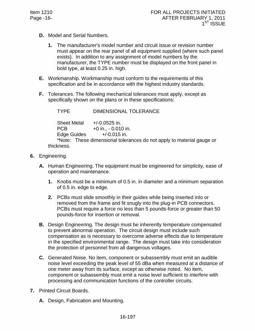
D. Model and Serial Numbers.
1. The manufacturer's model number and circuit issue or revision number must appear on the rear panel of all equipment supplied (where such panel exists). In addition to any assignment of model numbers by the manufacturer, the TYPE number must be displayed on the front panel in bold type, at least 0.25 in. high.
E. Workmanship. Workmanship must conform to the requirements of this specification and be in accordance with the highest industry standards.
F. Tolerances. The following mechanical tolerances must apply, except as specifically shown on the plans or in these specifications:
TYPE DIMENSIONAL TOLERANCE
Sheet Metal +/-0.0525 in. PCB +0 in., - 0.010 in.
Edge Guides +/-0.015 in. *Note: These dimensional tolerances do not apply to material gauge or
thickness.
6. Engineering.
A. Human Engineering. The equipment must be engineered for simplicity, ease of operation and maintenance.
1. Knobs must be a minimum of 0.5 in. in diameter and a minimum separation of 0.5 in. edge to edge.
2. PCBs must slide smoothly in their guides while being inserted into or removed from the frame and fit snugly into the plug-in PCB connectors. PCBs must require a force no less than 5 pounds-force or greater than 50 pounds-force for insertion or removal.
B. Design Engineering. The design must be inherently temperature compensated to prevent abnormal operation. The circuit design must include such compensation as is necessary to overcome adverse effects due to temperature in the specified environmental range. The design must take into consideration the protection of personnel from all dangerous voltages.
C. Generated Noise. No item, component or subassembly must emit an audible noise level exceeding the peak level of 55 dBa when measured at a distance of one meter away from its surface, except as otherwise noted. No item, component or subassembly must emit a noise level sufficient to interfere with processing and communication functions of the controller circuits.
7. Printed Circuit Boards.
A. Design, Fabrication and Mounting.
Item 1210 FOR ALL PROJECTS INITIATED Page -17- AFTER FEBRUARY 1, 2011 1ST ISSUE
17-197
1. All contacts on PCBs must be plated with a minimum thickness of 0.00003 in. gold over a minimum thickness of 0.000075 in. nickel.
2. PCB design must be such that when a component is removed and replaced, no damage is done to the board, other components, conductive traces or tracks.
3. Fabrication of PCBs must be in compliance with Military Specification MIL-P-13949, except as follows:
a. NEMA FR-4 glass cloth base epoxy resin copper clad laminates 0.0625 in. minimum thickness must be used. Inter-component wiring must be by laminated copper clad track having a minimum weight of 0.2 ounces per square foot with adequate cross section for current to be carried. All copper tracks must be plated or soldered to provide complete coverage of all exposed copper tracks. Jumper wires to external PCB components must be from plated-through padded holes and as short as possible.
b. All PCBs must conform to Section 3.3 of Military Specification MIL-P-13949G Grade of Pits and Dents, and be of Grade B quality (3.5.1.3) or better. The class of permissible bow or twist must be Class C (Table V) or better. The class of permissible warp or twist must be Class A (Table II) or better.
c. Sections 4.2 through 6.6 of Military Specification MIL-P-13949G (inclusive) must be omitted except as referenced in previous sections of this specification.
d. The mounting of parts and assemblies on the PCB must conform to Military Specification MIL-STD-275E, except as follows:
(1) Semiconductor devices that dissipate more than 250 milliwatts or cause a temperature rise of 10 degrees C, or more, be mounted with spacers, transipads or heat sinks to prevent contact with the PCB.
(2) When completed, all residual flux must be removed from the PCB.
(3) The resistance between any two isolated, independent conductor paths must be at least 100 Megohms when a 500 VDC potential is applied.
(4) All PCBs must be coated with a moisture resistant coating.
(5) Where less than 0.25 in. lateral separation is provided between the PCB (or the components of a PCB) and any metal surface, a 0.0625 in. (+/-0.0005 in.) Thick Mylar (polyester) plastic cover must be provided on the metal to protect the PCB.
Item 1210 FOR ALL PROJECTS INITIATED Page -18- AFTER FEBRUARY 1, 2011 1ST ISSUE
18-197
e. Each PCB connector edge must be chamfered at 30 degrees from board side planes. The key slots must also be chamfered so that the connector keys are not extracted upon removal of board or jammed upon insertion. The key slots must be 0.045 in. (+/-0.005 in.) for 0.1 in. spacing and 0.055 in. (+/-0.005 in.) for 0.156 in. spacing.
B. Soldering.
1. Hand soldering must comply with Military Specification MIL-STD-2000.
2. Automatic flow soldering must be a constant speed conveyor system with the conveyor speed set at optimum to minimize solder peaks or points. The temperature must be controlled to within +/-8 degrees C of the optimum temperature. The soldering process must result in the complete coverage of all copper runs, joints and terminals with solder except that which is covered by an electroplating process. Wherever clinching is not used, a method of holding the components in the proper position for the flow process will be provided.
3. If exposure to the temperature bath is of such a time-temperature duration as to come within 80% of any component's maximum specified time-temperature exposure, that component must be hand soldered to the PCB after the flow process has been completed.
C. Definitions. Definitions for the purpose of this section on PCBs must be taken from MIL-P-55110D Section 3.3 and any current addendum.
D. Jumpers. Jumpers are not allowed unless called out in the specifications or approved by the AGENCY.
8. Quality Control.
A. Components. All components must be lot sampled to assure a consistent high conformance standard to the design specification of the equipment.
B. Subassembly, Unit or Module. Complete electrical and environmental compliance testing must be performed on each module, unit, printed circuit or subassembly. Housing, chassis, and connection terminals must be inspected for mechanical sturdiness, and harnessing to sockets must be electrically tested for proper wiring sequence. The equipment must be visually and physically inspected to assure proper placement, mounting, and compatibility of subassemblies.
C. Pre-delivery Repair.
1. Any defects or deficiencies found by the inspection system involving mechanical structure or wiring must be returned through the manufacturing process or special repair process for correction.
Item 1210 FOR ALL PROJECTS INITIATED Page -19- AFTER FEBRUARY 1, 2011 1ST ISSUE
19-197
2. PCB flow soldering is allowed a second time if copper runs and joints are not satisfactorily coated on the first run. Under no circumstances will a PCB be flow soldered more than twice.
3. Hand soldering is allowed for printed circuit repair.
9. Electrical, Environmental and Testing Requirements. The framework of this section, along with the specific test requirements contained herein, is excerpted with modifications from NEMA TS2-2003 - Section 2 by permission of NEMA. Excerpt © 2002 AASHTO / ITE / NEMA.
A. General. This section establishes the limits of the environmental and operational conditions in which the Cabinet Assembly will perform. This section defines the minimum test procedures that may be used to demonstrate conformance of a device type with the provisions of the standard. These test procedures do not verify equipment performance under every possible combination of environmental requirements covered by this standard. Nothing in this testing profile must be construed as to relieve the requirement that the equipment provided must fully comply with these standards/specifications under all environmental conditions stated herein.
The Department may wish to extend the testing profile or introduce additional tests to verify compliance. (Authorized Engineering Information).
B. Inspection. A visual and physical inspection must include mechanical, dimensional and assembly conformance to all parts of this standard.
C. Testing Requirements.
1. A complete quality control / final test report must be supplied with each item. Quality control procedures must be submitted to the Department prior to production. The test report must indicate the name of the tester and be signed by a responsible manager.
2. The quality control procedure and test report format must be supplied to the Department for approval upon request. The quality control procedure must include the following, in the order shown:
a. Design Acceptance testing of all supplied components.
b. Physical and functional testing of all modules and items.
c. Environmental testing reports for all equipment.
d. Physical and functional testing of all items.
3. Separate certifications must be provided for Design and Production. Design Acceptance testing must be performed with a fully loaded and functional Cabinet Assembly. Production testing must be performed as part of the Department’s procurement delivery procedures and that testing should be performed at the Major Unit level. (Authorized Engineering Information).
Item 1210 FOR ALL PROJECTS INITIATED Page -20- AFTER FEBRUARY 1, 2011 1ST ISSUE
20-197
4. Certain portions of the test procedures contained in this standard my cause damage to the unit (e.g. protection devices may be aged) and are not recommended for routine Production testing. (Authorized Engineering Information)
D. Definitions of Major Units of the Cabinet Assembly. For the purpose of this section, "Major units of the Cabinet Assembly” must include the Controller Unit, Application Software for implementing the desired functionality, Cabinet Monitor Unit (CMU), Auxiliary Monitor Unit (AMU), Serial Interface Units (SIUs), Power Distribution Unit (PDA), Switch Packs, Flasher(s), and Detector(s).
E. Environmental and Operating Requirements. The requirements (voltage, temperature, etc.) of this section must apply in any combination.
1. Voltage and Frequency.
a. Operating Voltage. The nominal voltage must be 120 VAC, unless otherwise noted.
b. Operating Frequency. The operating frequency range must be 60 hertz (+/-3.0 hertz), unless otherwise noted.
2. Transients, Power Service. The Test Unit must maintain all defined functions when the independent test pulse levels specified below occur on the alternating-current power service.
3. Nondestructive Transient Immunity Requirements.
a. The Test Unit (with protection in place and operational) must be capable of withstanding a high energy transient having the following characteristics repeatedly applied to the alternating current input terminals (AC power applied) without failure of the test specimen:
(1) Amplitude: 2000 Volts (+/-5 percent), both positive and negative polarity.
(2) Energy Source: Capacitor, oil filled, 15 microfarads (+/-10 percent), internal surge impedance less than 1 ohm.
(3) Repetition: Applied to the Test Unit once every 2 seconds for a maximum of three applications for each polarity.
(4) After the foregoing, the Test Unit must perform all defined functions upon the application of nominal alternating current power.
This test is considered to be a minimum test requirement for the Test Unit complying with ANSI/IEEE C62.41 (100 Kilohertz Ring Wave, the 1.2/50 microseconds – 8/20 Combination Wave and the EFT Burst) at voltages and currents specified at “Location Category B2” and at “Test Severity” level III (i.e. up to 4.0 Kilovolts, open-circuit). Regional conditions may warrant additional testing as
Item 1210 FOR ALL PROJECTS INITIATED Page -21- AFTER FEBRUARY 1, 2011 1ST ISSUE
21-197
described in ANSI/IEEE C62.41. (Authorized Engineering Information)
4. Transients, Input-Output Terminals.
a. The Test Unit (without protection in place or operational) must maintain all defined functions, when the test pulse occurs on selected input-output terminals.
(1) Amplitude: 300 Volts, both positive and negative polarity.
(2) Pulse Source: 1000 ohms nominal impedance.
(3) Repetition: 1 pulse per second, for a minimum of 5 pulses per selected terminal.
(4) Pulse rise time: 1 microsecond.
(5) Pulse width: 10 microseconds.
This test is considered to be a minimum test requirement for the Test Unit complying with ANSI/IEEE C62.41. Regional conditions may warrant additional testing as described in ANSI/IEEE C62.41. (Authorized Engineering Information)
5. Temperature and Humidity. The Test Unit must maintain all programmed functions when the temperature and humidity ambients are within the specified limits defined herein.
a. Ambient Temperature.
(1) The operating ambient temperature range must be from -37 degrees C to +74 degrees C. The storage temperature range must be from -45 degrees C to +85 degrees C.
(2) The rate of change in ambient temperature must not exceed 18 degrees C per hour, during which the relative humidity must not exceed 95 percent.
b. Humidity.
(1) The relative humidity must not exceed 95 percent non-condensing over the temperature range of -37 degrees C to +74 degrees C.
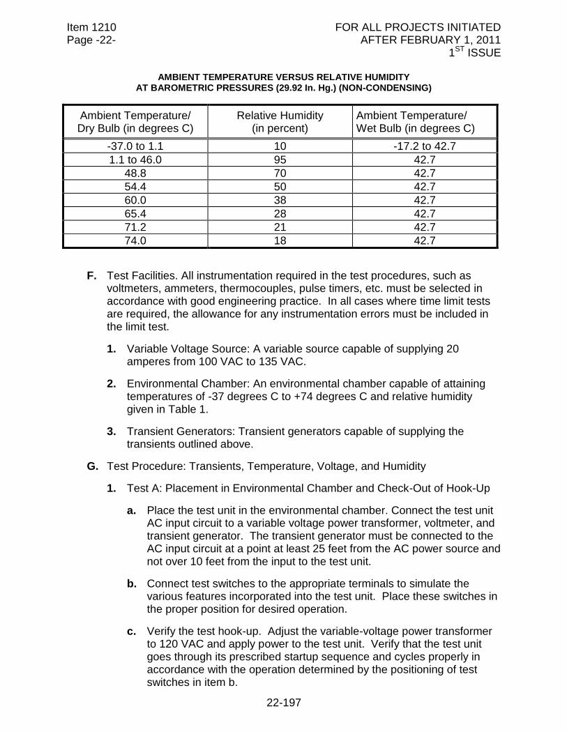
(2) Above +46 degrees C, constant absolute humidity must be maintained. This will result in the relative humidity shown in Exhibit 3-1 for dynamic testing.
Table 1
Item 1210 FOR ALL PROJECTS INITIATED Page -22- AFTER FEBRUARY 1, 2011 1ST ISSUE
22-197
AMBIENT TEMPERATURE VERSUS RELATIVE HUMIDITY AT BAROMETRIC PRESSURES (29.92 In. Hg.) (NON-CONDENSING)
Ambient Temperature/ Dry Bulb (in degrees C)
Relative Humidity (in percent)
Ambient Temperature/ Wet Bulb (in degrees C)
-37.0 to 1.1 10 -17.2 to 42.7
1.1 to 46.0 95 42.7
48.8 70 42.7
54.4 50 42.7
60.0 38 42.7
65.4 28 42.7
71.2 21 42.7
74.0 18 42.7
F. Test Facilities. All instrumentation required in the test procedures, such as voltmeters, ammeters, thermocouples, pulse timers, etc. must be selected in accordance with good engineering practice. In all cases where time limit tests are required, the allowance for any instrumentation errors must be included in the limit test.
1. Variable Voltage Source: A variable source capable of supplying 20 amperes from 100 VAC to 135 VAC.
2. Environmental Chamber: An environmental chamber capable of attaining temperatures of -37 degrees C to +74 degrees C and relative humidity given in Table 1.
3. Transient Generators: Transient generators capable of supplying the transients outlined above.
G. Test Procedure: Transients, Temperature, Voltage, and Humidity
1. Test A: Placement in Environmental Chamber and Check-Out of Hook-Up
a. Place the test unit in the environmental chamber. Connect the test unit AC input circuit to a variable voltage power transformer, voltmeter, and transient generator. The transient generator must be connected to the AC input circuit at a point at least 25 feet from the AC power source and not over 10 feet from the input to the test unit.
b. Connect test switches to the appropriate terminals to simulate the various features incorporated into the test unit. Place these switches in the proper position for desired operation.
c. Verify the test hook-up. Adjust the variable-voltage power transformer to 120 VAC and apply power to the test unit. Verify that the test unit goes through its prescribed startup sequence and cycles properly in accordance with the operation determined by the positioning of test switches in item b.
Item 1210 FOR ALL PROJECTS INITIATED Page -23- AFTER FEBRUARY 1, 2011 1ST ISSUE
23-197
Upon the satisfactory completion and verification of the test hook-up, proceed with Test B.
2. Test B: Nondestructive Transient Immunity:
a. Turn off the AC power input to the test unit from the variable-voltage power source.
b. Apply the following high-energy transient to the AC voltage input terminals of the test unit (no other power connected to terminals):
(1) Amplitude: 1000 V, both positive and negative polarity.
(2) Peak Power Discharge: Capacitor, oil-filled, 15 microfarads.
(3) Maximum Repetition Rate: Applied to the Cabinet Assembly once every 2 seconds for a maximum of three applications for each polarity.
c. Upon completion of the foregoing, apply 120 VAC to the test unit and verify that the test unit goes through its prescribed startup sequence and cycles properly in accordance with the programmed functions. The first operation of the over-current protective device during this test is not considered a failure of the test unit.
Item 1210 FOR ALL PROJECTS INITIATED Page -24- AFTER FEBRUARY 1, 2011 1ST ISSUE
24-197
Figure 2 Test Profile
NOTE—Test C through G follow the profile indicated in Figure 2 to demonstrate the ability of the test unit to function reliably under stated conditions of temperature, voltage, and humidity.
NOTES:
The rate of change in temperature must not exceed 18 degrees C per hour
Humidity controls must be set in conformance with the humidity given in Table 1 during the temperature change between Test D and Test E.
If a change in both voltage and temperature are required for the next test, the voltage must be selected prior to the temperature change.
3. Test C—Low-Temperature Low-Voltage Tests
a. Definition of Test Conditions
(1) Environmental Chamber Door: Closed.
40
30
10
20
0
10
70
60
50
40
30
20
80
DCA+B F GE
(AMBIENT)120 V
AC
120 V
AC
100 V
AC
135 V
AC
135 V
AC
100 V
AC
TE
MP
ER
AT
UR
E,
in D
EG
RE
ES
CE
LS
IUS
SEE NOTES
1 AND 3
SEE NOTES
1 AND 2
SEE NOTES
1 AND 3
X
XX
XX
X
Item 1210 FOR ALL PROJECTS INITIATED Page -25- AFTER FEBRUARY 1, 2011 1ST ISSUE
25-197
(2) Temperature: -37 degrees C.
(3) Low Voltage: 100 VAC.
(4) Humidity Control: Off.
b. Test Procedure: While at room temperature, adjust the input voltage to 100 VAC and verify that the test unit is still operable.
(1) With the test unit cycling through normal operations, lower the test chamber to -37 degrees C at a rate not exceeding 18 degrees C per hour. Allow the test unit to cycle for a minimum of 5 hours at -37 degrees C with the humidity controls in the off position. Then operate the test switches as necessary to determine that all functions are operable.
(2) Remove power from the test unit for a minimum period of 5 hours. Upon restoration of power, the test unit must go through its prescribed startup sequence and then resume cycling.
(3) With the test unit at -37 degrees C and the input voltage at 100 VAC, evaluate the following items against the respective standards:
(a) Power Interruption Tests
On satisfactory completion of this test, proceed with Test D.
4. Test D—Low-Temperature High-Voltage Tests
a. Definition of Test Conditions
(1) Environmental Chamber Door: closed.
(2) Low Temperature: -37 degrees C.
(3) High Voltage: 135 VAC.
(4) Humidity Controls: Off.
b. Test Procedure: While at -37 degrees C and with humidity controls off, adjust the input voltage to 135 VAC and allow the test unit to cycle for 1 hour. Then operate the test switches as necessary to determine that all functions are operable.
c. With the test unit at -37 degrees C and the input voltage at 135 VAC (humidity controls off), evaluate the following items against the respective standards:
(a) Power Interruption Tests
On satisfactory completion of this test, proceed to Test E.
5. Test E—High-Temperature High-Voltage Tests
Item 1210 FOR ALL PROJECTS INITIATED Page -26- AFTER FEBRUARY 1, 2011 1ST ISSUE
26-197
a. Definition of Test Conditions
(1) Environmental Chamber Door: Closed.
(2) High Temperature: +74 degrees C.
(3) High Voltage: 135 VAC.
(4) Humidity Controls: In accordance with the humidity given in Table 1.
b. Test Procedure—With the test unit cycling, raise the test chamber to +74 degrees C at a rate not to exceed 18 degrees C per hour. Verify the input voltage is 135 VAC.
c. Set the humidity controls to not exceed 95 percent relative humidity over the temperature range of +1.1 degrees C to +46 degrees C. When the temperature reaches +46 degrees C, readjust the humidity control to maintain constant absolute humidity; +42.7 degrees C wet bulb that results in the relative humidity shown in Table 1. Verify that the test unit continues to cycle satisfactory during the period of temperature increase and at established levels of relative humidity.
(1) Allow the test unit to cycle for a minimum of 15 hours at +74 degrees C and 18 percent relative humidity. Then operate the test switches as necessary to determine that all functions are operable.
(2) With the test unit at +74 degrees C and 18 percent relative humidity and the input voltage at 135 VAC, evaluate the following items against the respective standards:
(a) Power Interruption Tests
On satisfactory completion of this test, proceed to Test F.
6. Test F—High-Temperature Low-Voltage Tests
a. Definition of Test Conditions
(1) Environmental Chamber Door: Closed.
(2) High Temperature: +74 degrees C.
(3) Low Voltage: 100 VAC.
(4) Humidity Controls: 18 percent relative humidity and +42.7 degrees C wet bulb.
b. Test Procedure: Adjust the input voltage to 100 VAC and proceed to operate the test switches to determine that all functions are operable. With the test unit at +74 degrees C and 18 percent relative humidity, +42.7 degrees C wet bulb, and the input voltage at 100 VAC, evaluate the following items against the respective standards:
Item 1210 FOR ALL PROJECTS INITIATED Page -27- AFTER FEBRUARY 1, 2011 1ST ISSUE
27-197
(a) Power Interruption Tests
On satisfactory completion of this test, proceed to Test G.
7. Test G—Test Termination
a. Program the test unit to cycle.
b. Adjust the input voltage to 120 VAC.
c. Set the controls on the environmental chamber to return to room temperature, +20 degrees C (+/-5 degrees C), with the humidity controls in the off position. The rate of temperature change must not exceed 18 degrees C per hour.
d. Verify the test unit continues to cycle through normal operations properly.
e. Allow the test unit to stabilize at room temperature for 1 hour. Proceed to operate the test switches to determine that all functions are operable.
8. Test H—Appraisal of Equipment under Test
a. A failure is defined as any occurrence that results in other than normal operation of the equipment. (See item 2 for details.) If a failure occurs, the test unit must be repaired or components replaced, and the test during which failure occurred must be restarted from its beginning.
b. The test unit is considered to have failed if any of the following occur:
(1) If the test unit skips normal program intervals/steps or portions thereof when in normal operation, places false inputs, presents false outputs, exhibits disruption of normal sequence of operations, or produces changes in parameters beyond specified tolerances, or
(2) If the test unit fails to satisfy the requirements of Tests A to G, inclusive.
c. An analysis of the failure must be performed and corrective action taken before the test unit is retested in accordance with this standard. The analysis must outline what action was taken to preclude additional failures during the tests.
d. When the number of failures exceeds two, it must be considered that the test unit fails to meet these standards. The test unit may be completely retested after analysis of the failure and necessary repairs have been made in accordance with item c.
e. Upon completion of the tests, visually inspect the test unit. If material changes are observed which will adversely affect the life of the test unit, the cause and conditions must be corrected before making further tests.
Item 1210 FOR ALL PROJECTS INITIATED Page -28- AFTER FEBRUARY 1, 2011 1ST ISSUE
28-197
H. Power Interruption Test Procedures. Conduct the following power interruption tests at low input voltage (100 VAC) and high input voltage (135 VAC) at -37 degrees C, and +74 degrees C.
1. Short Power Interruption. While the Test Unit is cycling through normal operations, remove the input voltage for a period not to exceed 475 milliseconds. Upon restoration of the input voltage, check to insure that the Test Unit continues normal operation as though no power interruption has occurred. Repeat this test three times.
2. Voltage Variation. All circuits of the Test Unit must be subjected to slowly varying line voltage during which the Test Unit must be subjected to line voltage that is slowly lowered from a nominal 120 VAC line voltage to 0 VAC at a rate of not greater than 2 Volts per second. The line voltage must then be slowly raised to 100 VAC at which point the Test Unit must resume normal operation without operator intervention. Perform this test at both -37 degrees C and +74 degrees C, at a nominal 120 VAC line voltage. Repeat this test three times.
3. Rapid Power Interruption. Subject the Test Unit to rapid power interruption testing of the form that the power is off for 350 milliseconds and on for 650 milliseconds for a period of 2 minutes. Perform power interruption through electromechanical contacts of an appropriate size for the load. During this testing, the controller must function normally and continue normal sequencing (operation) at the conclusion of the test. This test must be performed at both -37 degrees C and +74 degrees C, at a nominal 120 VAC line voltage. Repeat this test three times.
10. Auxiliary Cabinet Units.
A. General Requirements.
1. Models 200 and 204 General.
a. The unit chassis must be made of metal suitable to meet rigid support and environmental requirements. Where electrical isolation is the only requirement, plastic insulation material may be used in lieu of metal.
b. The unit control circuitry and switches must be readily accessible by the use of a screwdriver or wrench. Only one type of screw head end (Slotted or Phillips) to be used.
c. The unit must be constructed so that no live voltage is exposed. A handle must be attached to the front panel for insertion or removal from the unit mating connector.
d. The unit must be so constructed that its lower surface must be no more than 2.06 in. below the centerline of the connector and no part extend more than 0.9 in. to the left or 1.1 in. to the right of the connector centerline.
Item 1210 FOR ALL PROJECTS INITIATED Page -29- AFTER FEBRUARY 1, 2011 1ST ISSUE
29-197
e. Continuous edge guides must be provided on the unit.
f. Each switch must be capable of switching any current from 0.050 Amperes to 10.0 Amperes (AC) load with power factor of 0.85 or higher.
g. Unit indicators must be vertically centered on the front panel with indicators positioned no more than 1 in. from said center.
2. Model Plug Connectors. Model plug connectors must be:
a. Model 200 BEAU P 5412 - LAB or approved equal.
b. Model 204 BEAU P 5406 - LAB or approved equal.
B. Model 200 Switch Pack Unit.
1. General.
a. The Model 200 Switch Pack Unit must be a modular plug-in device containing three solid-state switches. Each switch must open or close a connection between applied power and external load.
b. A Ground True Controller Unit Input (0 VDC to 6 VDC) must cause the switch to conduct (ON) and a Ground False (16 VDC or more) must cause it to not conduct (OFF), State transition must occur between 6 VDC and 16 VDC. The input must not sink more than 20 milliamperes or be subjected to more than 30 VDC. The input must have reverse polarity protection.
c. With all switches ON, the unit must not draw more than 60 milliamperes at +16 VDC or more from the +24 VDC cabinet power supply.
d. Each switch must have an OFF state dv/dt rating of 100 Volts per microsecond or better. Each switch must provide isolation between inputs and outputs of at least 2000 Vdc and at least 100 megaohms resistive.
e. The unit front panel must have an indicator on the input to each switch. The indicator must be labeled or color-coded “Red”-top switch, “Yellow”-middle switch, and “Green”-bottom switch. The middle switch indicator must be vertically centered on the unit front panel with the other indicators positioned 1 in. above and below.
f. The resistance between the AC+ input terminal and the AC+ output terminal of each switch must be a minimum of 15K Ohms when the switch is in open (OFF) state. When the switch is in the OFF state, the output current through the load must not exceed 10 milliamperes peak.
C. Model 204 Flasher Unit and Model 205 Flash Transfer Relay Unit.
1. Model 204 Flasher Unit.

Item 1210 FOR ALL PROJECTS INITIATED Page -30- AFTER FEBRUARY 1, 2011 1ST ISSUE
30-197
a. The FLASHER UNIT must be a modular plug-in device containing a flasher control circuit and two solid-state switches. The unit’s function is to alternatively open and close connections between applied power and external load.
b. The unit must generate its own internal DC power from the AC Line.
c. The unit must commence flashing operation when AC power is applied providing 50 to 60 flashes per minute per switch with a 50 % duty cycle.
d. Each switch must have an OFF state dv/dt rating of 200 V/microsecond or better. The resistance between the AC+ input terminal and the AC+ output terminal of each switch must be a minimum of 15K Ohms when the switch is in open (OFF) state. When the switch is in OFF state the output current must not exceed 10 milliamperes peak.
e. An indicator showing each switch output state must be provided. The two indicators must be centered with 1 in. minimum spacing.
f. Each circuit must be designed to operate in an open-circuit condition without load for 10 years minimum.
g. A surge arrestor must be provided between AC (pin 11) and Flasher Output (pins 7 & 8). The arrestor must meet the following requirements:
Recurrent Peak Voltage 212 Volts Maximum Energy Rating 50 Joules Average Power Dissipation 0.85 Watts Peak I for pulses less than 6 microseconds 2000 Amperes Standby I less than 1 Ma
2. Model 205 Flash Transfer Relay Unit. Each switch must be designed for a minimum of 100,000 (reference is a 10-year lifespan) operations while switching a tungsten load of 1000 Watts at 70 degrees C. Switch isolation between DC input and AC output circuit must be at least 10,000 Megohms at 2000 VDC.
a. The Flash Transfer Relay Unit must be of electromechanical type, designed for continuous duty.
b. Each unit must be enclosed in a removable, clear plastic cover. The manufacturer’s name, electrical rating, and part number must be placed on the cover. They must be durable, permanent and readily visible.
c. Each unit must be provided with DPDT contacts. The contact points must be of fine silver, silver alloy or a superior alternate material. Contact points and arms must be capable of switching 20 Amperes or 1 Kilowatt Tungsten Load at 120 VAC per contact at least 100,000 operations without contact welding or excessive burning, pitting or cavitation. The points and arms must be able to withstand 10 Gs, 10 –55 Hertz without contact chatter.
Item 1210 FOR ALL PROJECTS INITIATED Page -31- AFTER FEBRUARY 1, 2011 1ST ISSUE
31-197
d. The relay coil must have a power consumption of 10 Volt - Ampere maximum.
e. Each relay must withstand a potential of 1500 VAC at 60 Hertz between insulated parts and between current carrying or non-carrying parts. Each relay must have a one cycle surge rating of 175 Amperes RMS and pickup and drop out within 20 milliseconds.
D. Model 212 ITS Cabinet Monitor Unit (CMU).
1. General. The CMU is the principle part of the ITS Cabinet Monitoring System. It is resident in the Power Distribution Assembly. The role of the CMU is to query various cabinet conditions and, if the application requires action, the CMU will transfer control from the ATC Controller Unit to a safe control mode, examples include Signalized Intersection, Ramp Metering or other applications. Some applications may not require any action, only data gathering and report back to the ATC Controller Unit.
The CMU is composed of a microprocessor, memory devices including non-volatile memory, communications circuitry to interface with Serial Buses #1 and #3, front panel indicators, front panel communication connector and a serial memory key device. The Operating Program must be resident in the Non-volatile memory. The serial memory key Memory must possess the conditions and function selections of the Unit.
2. Traffic Control Application. The Model 212 is intended for traffic control applications.
3. Failed State Action (FSA). Only Unit Reset must reset the CMU from a LATCHED FAILED STATE ACTION (LFSA). Only a Unit Reset or a CMU Power Fail must reset a LATCHED RESETTABLE FAILED STATE ACTION (LFSA-R).
A NONLATCHED FAILED STATE ACTION (NFSA) must be reset if the fault conditions causing the NFSA have been removed. An NFSA must last for the programmed Minimum Flash time at a minimum.
Only one LFSA, LFSA-R or NFSA fault state must be set at any time.
4. Unit Reset. The CMU must be reset from a FSA as a result of the front panel reset button or the EXTERNAL TEST RESET input. This reset command must be a one-time event, such that a continuous reset command does not prevent the CMU from operating. The EXTERNAL TEST RESET input must be isolated from the AC+ Raw circuitry.
The EXTERNAL TEST RESET input must be True when the voltage is less than 8 VDC. The EXTERNAL TEST RESET input must be False when the voltage is greater than 16 VDC. A minimum True pulse width on the EXTERNAL TEST RESET input of 100 milliseconds is required for a Unit Reset.
Item 1210 FOR ALL PROJECTS INITIATED Page -32- AFTER FEBRUARY 1, 2011 1ST ISSUE
32-197
5. Exit From Failed State Action. Prior to the CMU transferring the Output Relay contacts from the Fault state to the No Fault state, a transition period of 500 milliseconds must occur. During the transition period the Output Relay contacts must be in the Fault state and the CMU must set the Start-Up Flash Call bit in the Type 189 Frame to 1. At all other times the Start-Up Flash Call bit of the Type 189 Frame must be set to 0.
6. Monitor Functions.
a. Cabinet Power Supply. The CMU must sense the Cabinet +24 VDC and +12 VDC power supply sources to +/-5% accuracy. The CMU must also sense the Cabinet +24 VDC state in each Output Assembly as reported by each AMU. Voltages equal to or greater than +22 VDC and +11 VDC respectively must NOT cause a LFSA. Voltages at or less than +18 VDC and +9 VDC for 500 milliseconds or longer must cause a LFSA. If the sensed voltage is less than +22 VDC or +11 VDC for 200 milliseconds or less, the CMU must NOT cause a LFSA. All other timing or voltage conditions may or may not cause LFSA. A +24 VDC failure or +12 VDC failure during the programmed Minimum Flash time or during a CMU Power Failure must not cause a LFSA. The CMU must report the value of the +24 VDC and +12 VDC power supply sources in the Type 189 response frame.
There must be programming in the serial memory key to disable +12 VDC power supply monitoring.
b. Conflicting Channels. For purpose of conflict determination, an active signal on either of the Green/Walk or Yellow inputs associated with any of the thirty-two channels must be considered as that channel being active. The serial memory key must contain the permissive channel pair programming. When any conflicting channels are detected as concurrently active for less than 200 milliseconds the CMU must not cause a LFSA. When any conflicting channels are detected as concurrently active for 500 milliseconds or more, the CMU must cause a LFSA. When any conflicting channels are detected as concurrently active for more than 200 milliseconds but less than 500 milliseconds, the CMU may or may not cause a LFSA. The time interval between the beginning of the concurrently conflicting channels and the transfer to the LFSA must not exceed 500 milliseconds.
c. Serial Bus Error. The CMU communicates with both Serial Bus (SB) #1 and #3. In SB #1 the CMU is a Secondary, polled by the ATC Controller Unit Primary. On SB #1, the CMU must respond to the Serial Bus #1 Address defined by the ADDRESS 0 and ADDRESS 1 pins. In SB #3 the CMU is the Primary, polling each AMU Secondary.
(1) Serial Bus #1 Error. The CMU must cause a FSA when a Type 61 or Type 67 Frame has not been received from the ATC Controller Unit for greater than 1000 milliseconds. The first and second failures in a 24-hour period must be a NFSA. The third failure in a
Item 1210 FOR ALL PROJECTS INITIATED Page -33- AFTER FEBRUARY 1, 2011 1ST ISSUE
33-197
24-hour period must be a LFSA-R. If a CMU Power Fail resets the LFSA-R, the SB #1 timeout count must be reset to 2 such that the next SB #1 timeout results in a LFSA-R.
A SB #1 timeout failure during the programmed Minimum Flash time or during a CMU Power Failure must not cause a FSA. The SB #1 Timeout function must be disabled if the SB #1 DISABLE input is at a True (Low) state.
The SB #1 DISABLE input must be True when the voltage is less than 8 VDC. The SB #1 DISABLE input must be False when the voltage is greater than 16 VDC. The SB #1 DISABLE input must be isolated from the AC+ Raw circuitry.
(2) Serial Bus #3 Error. The CMU must cause a FSA when a Type 129 or Type 130 Frame has not been received from each AMU for greater than 300 milliseconds. The first and second failures in a 24-hour period must be a NFSA. The third failure in a 24-hour period must be a LFSA-R. If a CMU Power Fail resets the LFSA-R, the SB #3 timeout count must be reset to 2 such that the next SB #3 timeout results in a LFSA-R. A SB #3 timeout failure during the programmed Minimum Flash time or during a CMU Power Failure must not cause a FSA.
d. Type 62 – Send to Local Flash Command Message. If the “N” bit is set in a Type 62 – Send to Local Flash Command message, the CMU must react by causing a NFSA. The NFSA must remain until the receipt of a Type 62 – Send to Local Flash Command message with the “N” bit cleared or until the CMU is reset by a Unit Reset or CMU Power Fail. The NFSA must last for the programmed Minimum Flash time at a minimum. If the “L” bit is set in a Type 62 – Send to Local Flash Command message, the CMU must react by causing a LFSA.
e. Diagnostics.
(1) Diagnostics Error. The CMU must be provided with a resident series of self-check diagnostic capabilities. The CMU must contain provisions to verify all memory elements on power-up. When a fault is detected, the LFSA-R must be set and the DIAGNOSTIC indicator illuminated.
(2) RAM Diagnostic. This test must verify that all RAM elements are operating correctly at power-up or following a Unit Reset. Patterns must be written to RAM. Each write must be followed by a read to verify that it contains the written pattern.
(3) Nonvolatile Diagnostic. This test must verify that the nonvolatile ROM(s) contain the proper program. The routine must perform a check on each ROM and make a comparison with a preprogrammed check value. This test must be performed at
Item 1210 FOR ALL PROJECTS INITIATED Page -34- AFTER FEBRUARY 1, 2011 1ST ISSUE
34-197
power-up and at a minimum rate of 1024 bits per second during operation.
(4) Serial Memory Key Memory Diagnostic. This test must verify whether the non-volatile serial memory key contains valid data and that the data has not changed since the last write. The routine must perform a check on each nonvolatile memory element at power-up and whenever read and make a comparison with a preprogrammed check value. The serial memory key not present must cause a LFSA if the DOOR SWITCH FRONT input is sensed as not active (door closed).
(5) Internal MPU Monitor. The CMU must monitor the operation of its microprocessor with an independent circuit. At a minimum, the monitoring circuit must receive logic state transitions at least once every 50 milliseconds from the microprocessor. When the logic state transition is not received for 500 milliseconds the monitor circuit must force a LFSA-R and illuminate the DIAGNOSTIC indicator.
f. Multiple Input. The CMU must be capable of monitoring for the presence of an active signal on two or more inputs of a channel. When the presence of an active signal on two or more inputs of a channel is detected for less than 200 milliseconds, the CMU must not cause a LFSA. When the presence of an active signal on two or more inputs to a channel is detected for 450 milliseconds or more, the CMU must cause a LFSA. When the presence of an active signal on two or more inputs to a channel is detected for more than 200 milliseconds but less than 450 milliseconds, the CMU may or may not cause a LFSA. Multiple Input monitoring must be disabled when the MAIN CONTACTOR COIL STATUS input is not active. There must be programming in the serial memory key to disable Multiple Indication monitoring on a color combination basis (G+Y, Y+R, G+R).
g. Lack of Signal Inputs. The unit must detect the absence of any required signal voltage OR signal current (CSU) on the inputs of a channel. For voltage purposes a required signal on the Green or Yellow or Red inputs associated with a channel must be considered as that channel being active. When an absence of an active channel is detected for less than 700 milliseconds, the CMU must not cause a LFSA. When an absence of an active channel is detected for 1000 milliseconds or more, the CMU must cause a LFSA. When an absence of an active channel is detected for more than 700 milliseconds but less than 1000 milliseconds, the CMU may or may not cause a LFSA. Lack of Signal Input monitoring must be disabled for all channels when the MAIN CONTACTOR COIL STATUS input is not active. There must be programming in the serial memory key to disable Lack of Signal Input monitoring on a per channel basis.
Item 1210 FOR ALL PROJECTS INITIATED Page -35- AFTER FEBRUARY 1, 2011 1ST ISSUE
35-197
Lack of Signal Input monitoring must also be disabled for any channel which has the DARK CHANNEL MAP bit set to "1" in the serial memory key programming for the DARK CHANNEL MAP addressed by the DARK CHANNEL MAP SELECT bits in a Type 61 message. The CSU monitor function is hardwired to twenty-eight physical channels, thus Virtual Channels do not have CSU monitoring capability. The CSU monitor function must be disabled for any physical channel that has an input remapped to a Virtual Channel.
h. Yellow Clearance. The CMU must verify that the Yellow Change interval is at least 2.7 seconds (+/-0.1 seconds). When the minimum Yellow Change interval is not satisfied, the CMU must cause a LFSA. The CMU must report a Skipped Yellow Clearance when the Yellow Change interval is less than 100 milliseconds. The CMU must report a Short Yellow Clearance when the Yellow Change interval is less than 2.7 seconds (+/-0.1 seconds) and greater than 100 milliseconds.
Minimum Yellow Change interval monitoring must be disabled when the MAIN CONTACTOR COIL STATUS input is not active. There must be programming in the serial memory key to disable Minimum Yellow Change interval monitoring on a per channel basis.
i. Yellow Plus Red Clearance. The CMU must verify that the Yellow Change plus Red Clearance interval between the end of an active GREEN signal and the beginning of the next conflicting GREEN signal is at least 2.7 (+/-0.1 seconds). When the minimum Yellow Change plus Red Clearance interval is not satisfied, the CMU must cause a LFSA. Minimum Yellow Change plus Red Clearance monitoring must be disabled when the MAIN CONTACTOR COIL STATUS input is not active. There must be programming in the serial memory key to disable Minimum Yellow Change plus Red Clearance interval monitoring on a per channel basis.
j. Local Flash Status. The CMU must monitor the LF STATUS input. When this signal is sensed as not active for greater than 500 milliseconds, the CMU must cause a NFSA. When this signal is sensed as not active for less than 200 milliseconds, the CMU must not cause a NFSA.
(1) Local Flash Status Recovery. Recovery from Local Flash Status NFSA must occur when this signal is sensed as active for greater than 500 milliseconds. When this signal is sensed as active for less than 200 milliseconds, the CMU must not cause recovery from Local Flash Status NFSA.
k. Circuit Breaker Trip Status. The CMU must monitor the CB TRIP STATUS input. When this signal is sensed as not active for greater than 500 milliseconds, the CMU must cause a LFSA. When this signal is sensed as not active for less than 200 milliseconds, the CMU must not cause a LFSA.
Item 1210 FOR ALL PROJECTS INITIATED Page -36- AFTER FEBRUARY 1, 2011 1ST ISSUE
36-197
l. Flasher Unit Output Failed. The CMU must monitor the FLASHER 1-1, FLASHER 1-2, FLASHER 2-1, and FLASHER 2-2 voltage states reported by each AMU. These inputs must be considered active when the input voltage exceeds 89 Volts RMS. These inputs must not be considered active when the input voltage is less than 70 Volts RMS. Signals between 89 Volts RMS and 70 Volts RMS may or may not be considered active. When a transition from the inactive state to the active state or a transition from the active state to the inactive state is absent for greater than 2500 milliseconds, the CMU must set a status bit in the Type 189 frame. This alarm condition must not cause a FSA. It should cause the appropriate response in the ATC Controller Unit. This status is non-latching, such that once a status bit has been set, the sensing of five valid transitions of the input must clear the status bit.
m. CMU Power Failure. The CMU must monitor the AC+ Raw input and the NRESET and POWERDOWN cabinet control inputs to determine a CMU Power Failure response. The POWERDOWN signal in the low state indicates loss of AC+ Raw in the Controller Unit. A CMU Power Failure must be recognized when both the POWERDOWN and NRESET signals are active low for greater than 100 milliseconds or the AC+ Raw voltage is less than 82 Volts RMS (+/-2 Volts RMS).
n. AC+ Raw Level Sense. The CMU must monitor the AC+ Raw input and AC+ Raw inputs reported by each AMU. When any AC+ Raw voltage is less than 82 Volts RMS (+/-2 Volts RMS) for greater than 650 milliseconds (+/-100 milliseconds) the CMU must cause a NFSA. Once NFSA has been set, the POWERDOWN and NRESET signals must not be monitored until all AC+ Raw voltages have exceeded 87 Volts RMS (+/-2 Volts RMS).
o. Power Interrupt. The CMU must disable monitoring of the +12VDC and +24VDC power supply inputs when either the POWERDOWN or NRESET input is low. When the POWERDOWN and NRESET signals are both low the CMU must cause a NFSA.
p. Power Recovery. When the POWERDOWN input is high and the NRESET signal goes from low to high the CMU must begin timing the programmed Minimum Flash Interval. During the Minimum Flash Interval the CMU must be in NFSA.
q. Power Up. Following initial application of AC+ Raw voltage the CMU must maintain a NFSA until the POWERDOWN input is high and the NRESET signal goes from low to high. The CMU must then begin timing the programmed Minimum Flash Interval. During the Minimum Flash Interval the CMU must be in NFSA.
r. Minimum Flash Interval. The CMU must be in NFSA during the Minimum Flash Interval. The Minimum Flash Interval must be programmed in the serial memory key between the limits of 6 seconds
Item 1210 FOR ALL PROJECTS INITIATED Page -37- AFTER FEBRUARY 1, 2011 1ST ISSUE
37-197
to 16 seconds with an incremental adjustment of 1 second. The CMU must not set a FSA during the Minimum Flash Interval.
7. Field Output Check.
a. Field Check Mode. The CMU must compare the active states of the field signals with the states reported by the ATC Controller Unit in the Type 61 frame. When a mismatch is detected for less than 700 milliseconds the CMU must not cause a LFSA. When a mismatch is detected for 1000 milliseconds or more, the CMU must cause a LFSA. When a mismatch is detected for more than 700 milliseconds but less than 1000 milliseconds, the CMU may or may not cause a LFSA. Field Output Check monitoring must be disabled when the MAIN CONTACTOR COIL STATUS input is not active. There must be a programming in the serial memory key to disable Field Output Check monitoring on a field input basis.
b. Field Check Status. The CMU must compare the active states of the field signals with the states reported by the ATC Controller Unit in the Type 61 frame. When a mismatch is detected while a Conflict, Lack of Signal, or Multiple fault is timing, Field Check Status must be reported with the fault to indicate the faulty channel(s) and color(s). Field Output Check monitoring must be disabled when the MAIN CONTACTOR COIL STATUS input is not active. There must be a programming in the serial memory key to disable Field Output Check monitoring on a field input basis.
8. CMU Temperature. The CMU must measure the temperature at the CMU and report this value in the Type 182 frame. Temperature accuracy must be +/-6 degrees C over the operating temperature range of the CMU.
9. Input Signals.
a. Field Signal Inputs. A Green or Yellow signal input must be sensed active when it exceeds 25 Volts RMS and must not be sensed active when it is less than 15 Volts RMS. A Green or Yellow signal between 15 Volts RMS and 25 Volts RMS may or may not be sensed active. There must be a programming in the serial memory key to disable the Yellow input for each physical channel. A Red signal input must be sensed active when it exceeds 70 Volts RMS and must not be sensed active when it is less than 50 Volts RMS. A Red signal between 50 Volts RMS and 70 Volts RMS may or may not be sensed active.
b. Switch Pack Current. A channel must be sensed active when the load current exceeds 105% of the Channel Current Sense Threshold programmed for that channel in the serial memory key. A channel must not be sensed active when the load current is less than 95% of the Channel Current Sense Threshold programmed for that channel in the serial memory key. A load current value between 95% and 105% of the Channel Current Sense Threshold may or may not be sensed active.
Item 1210 FOR ALL PROJECTS INITIATED Page -38- AFTER FEBRUARY 1, 2011 1ST ISSUE
38-197
c. PDA Control Signal Inputs.
(1) Local Flash Status. This input must be internally connected to the CMU Output Relay COM pin. This input must be considered active when the input voltage exceeds 89 Volts RMS. This input must not be considered active when the input voltage is less than 70 Volts RMS. Signals between 89 Volts RMS and 70 Volts RMS may or may not be considered active. Operation of the cabinet in AUTO mode must place AC+ on this input. Operation of the cabinet in FLASH mode must be open circuit on this input. The CMU must report the state of this input in the Type 189 frame.
(2) Main Contactor Coil Status. The MAIN CONTACTOR COIL STATUS input must be connected to the AC+ Raw side of the main contactor signal bus relay coil. An active signal on this input indicates the Signal Bus should be powering the Switch Packs. This input must be considered active when the input voltage exceeds 89 Volts RMS. This input must not be considered active when the input voltage is less than 70 Volts RMS. Signals between 89 Volts RMS and 70 Volts RMS may or may not be considered active. The CMU must report the state of this input in the Type 189 frame.
(3) Main Contactor Secondary Status. The MAIN CONTACTOR SECONDARY STATUS input must be connected to the output side of the main contactor signal bus relay. This input must be considered active when the input voltage exceeds 89 Volts RMS. This input must not be considered active when the input voltage is less than 70 Volts RMS. Signals between 89 Volts RMS and 70 Volts RMS may or may not be considered active. The CMU must report the state of this input in the Type 189 frame.
(4) FTR Coil Drive Status. The FTR COIL DRIVE STATUS input must be connected to the FTR COIL DRIVE signal in the AC SIGNAL POWER BUS. This input must be considered active when the input voltage exceeds 89 Volts RMS. This input must not be considered active when the input voltage is less than 70 Volts RMS. Signals between 89 Volts RMS and 70 Volts RMS may or may not be considered active. The CMU must report the state of this input in the Type 189 frame.
(5) Circuit Breaker (CB) Trip Status. The CB TRIP STATUS input must be connected to the Auxiliary Switch output of the circuit breaker unit. This input must be considered active when the input voltage exceeds 89 Volts RMS. This input must not be considered active when the input voltage is less than 70 Volts RMS. Signals between 89 Volts RMS and 70 Volts RMS may or may not be considered active. The CMU must report the state of this input in the Type 189 frame.
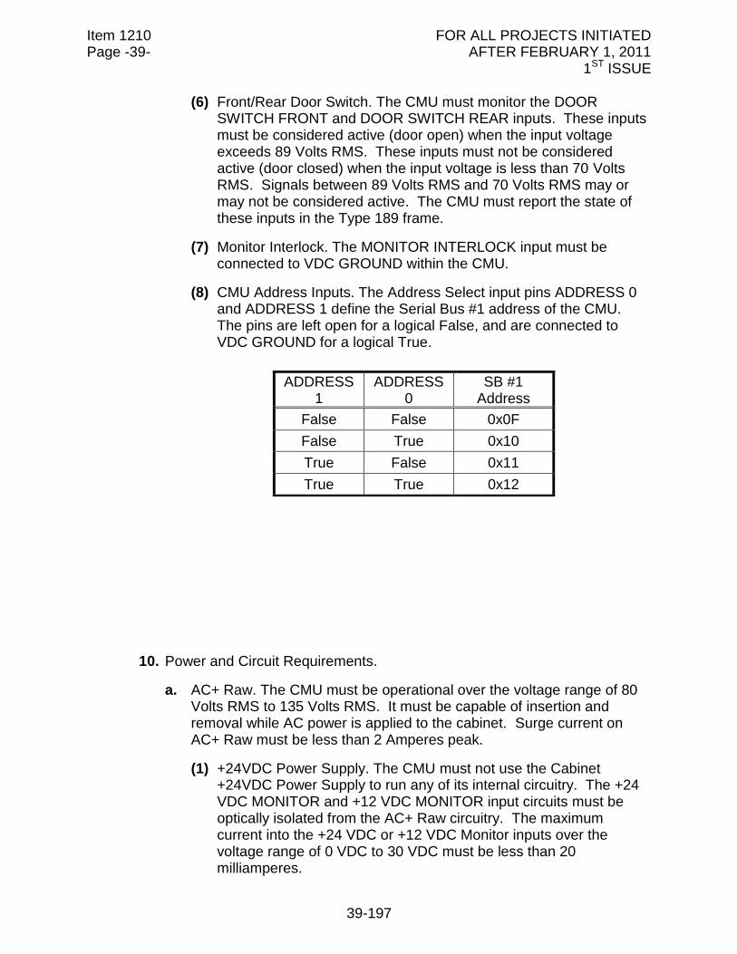
Item 1210 FOR ALL PROJECTS INITIATED Page -39- AFTER FEBRUARY 1, 2011 1ST ISSUE
39-197
(6) Front/Rear Door Switch. The CMU must monitor the DOOR SWITCH FRONT and DOOR SWITCH REAR inputs. These inputs must be considered active (door open) when the input voltage exceeds 89 Volts RMS. These inputs must not be considered active (door closed) when the input voltage is less than 70 Volts RMS. Signals between 89 Volts RMS and 70 Volts RMS may or may not be considered active. The CMU must report the state of these inputs in the Type 189 frame.
(7) Monitor Interlock. The MONITOR INTERLOCK input must be connected to VDC GROUND within the CMU.
(8) CMU Address Inputs. The Address Select input pins ADDRESS 0 and ADDRESS 1 define the Serial Bus #1 address of the CMU. The pins are left open for a logical False, and are connected to VDC GROUND for a logical True.
10. Power and Circuit Requirements.
a. AC+ Raw. The CMU must be operational over the voltage range of 80 Volts RMS to 135 Volts RMS. It must be capable of insertion and removal while AC power is applied to the cabinet. Surge current on AC+ Raw must be less than 2 Amperes peak.
(1) +24VDC Power Supply. The CMU must not use the Cabinet +24VDC Power Supply to run any of its internal circuitry. The +24 VDC MONITOR and +12 VDC MONITOR input circuits must be optically isolated from the AC+ Raw circuitry. The maximum current into the +24 VDC or +12 VDC Monitor inputs over the voltage range of 0 VDC to 30 VDC must be less than 20 milliamperes.
ADDRESS 1
ADDRESS 0
SB #1 Address
False False 0x0F
False True 0x10
True False 0x11
True True 0x12
Item 1210 FOR ALL PROJECTS INITIATED Page -40- AFTER FEBRUARY 1, 2011 1ST ISSUE
40-197
(2) Failed State Output Circuit. The Output relay of the CMU must have one set of isolated Form C contacts. These relay contacts must be rated for a minimum of 3 Amperes at 120 Volts RMS and 100,000 operations. Contact opening/closing time must be 30 milliseconds or less. The relay coil must be energized in the No Fault state and de-energized in the FSA state.
11. Front Panel Devices.
a. Indicators. All indicators must be clear LEDs. Clear LEDs must not depend on a reflector or diffusion as part of its design. Clear LEDs must only show the die and not appear to be ON when exposed to ambient light. The following indicators must be provided (Top to Bottom).
b. Power. A green POWER indicator must illuminate to indicate AC+ Raw voltage is proper. It must flash at a 2 Hertz rate when the NRESET or POWERDOWN input is True. It must remain off when the voltage is less than 80 Volts RMS (+/-2 Volts RMS).
c. 24 VDC Fail. A red 24VDC FAIL indicator must illuminate when the CMU is in FSA as a result of a 24VDC cabinet power supply fault.
d. 12 VDC Fail. A red 12VDC FAIL indicator must illuminate when the CMU is in FSA as a result of a 12VDC cabinet power supply fault. The 12VDC FAIL indicator must flash at a 2 Hertz rate when the 12 VDC monitor function is disabled.
e. Conflict. A red CONFLICT indicator must illuminate when the CMU is in FSA as a result of a Conflicting Channels fault.
f. Lack of Signal. A red LACK OF SIGNAL indicator must illuminate when the CMU is in FSA as a result of a Lack of Signal Inputs fault.
g. Multiple. A red MULTIPLE indicator must illuminate when the CMU is in FSA as a result of a Multiple Inputs fault.
h. ATC/Local Flash. A red ATC/LOCAL FLASH indicator must illuminate when the CMU is in FSA as a result of a Type 62 – Send to Local Flash Command from the ATC Controller Unit, the LOCAL FLASH STATUS input sensed inactive, or CB TRIP STATUS active.
i. Clearance. A red CLEARANCE indicator must illuminate when the CMU is in FSA as a result of a Yellow Clearance or Yellow Plus Red Clearance fault.
j. Field Check. A red FIELD CHECK indicator must illuminate when the CMU is in FSA as a result of a Field Output Check fault. The indicator must flash at a 2 Hertz rate when the CMU is in FSA with Field Check Status as a result of Conflict, Lack of Signal, or Multiple fault.
Item 1210 FOR ALL PROJECTS INITIATED Page -41- AFTER FEBRUARY 1, 2011 1ST ISSUE
41-197
k. SB #1 Error. A red SB #1 ERROR indicator must illuminate when the CMU is in FSA as a result of a Serial Bus #1 fault.
l. SB #3 Error. A red SB #3 ERROR indicator must illuminate when the CMU is in FSA as a result of a Serial Bus #3 fault.
m. Diagnostic. A red DIAGNOSTIC indicator must illuminate when the CMU is in FSA as a result of a Diagnostic fault. The DIAGNOSTIC indicator must flash at a 4 Hertz rate if the serial memory key is not present and a FSA state does not exist.
n. SB #1 Rx. A yellow indicator must illuminate for 40 milliseconds (+/-5 milliseconds) each time the CMU correctly receives a frame on Serial Bus #1.
o. SB #3 Rx. A yellow indicator must illuminate for 40 milliseconds (+/-5 milliseconds) each time the CMU correctly receives a frame on Serial Bus #3.
12. Serial Bus #3 Terminations. The Serial Bus #3 RxD+ input must be terminated on the CMU to the Serial Bus #3 EIA-485 supply voltage through a 560 Ohm resistor. The Serial Bus #3 RxD- input must be terminated on the CMU to AC Raw- through a 560 Ohm resistor. A 120 Ohm resistor must be connected on the CMU between RxD+ and RxD-. The CMU Serial Bus #3 TxD drivers must remain in the mark state with drivers enabled when the CMU is not transmitting a command frame. Note: A 120 Ohm resistor must be connected between TxD+ and TxD- on the Serial Bus #3 cable assembly in the last Output Assembly installed in the Serial Bus #3 daisy chain.
13. Terminal Port. An EIA-232-E Data Terminal Equipment (DTE) interface and connector must be provided for interconnecting to a personal computer. Where differences occur between the EIA-232 standard and this document, this document must govern.
a. Physical. The connector must be mounted on the front panel and must be a 9-position subminiature D-type connector with metal shell. The connector must utilize female contacts with 15 millionths of an inch gold plating in the mating areas.
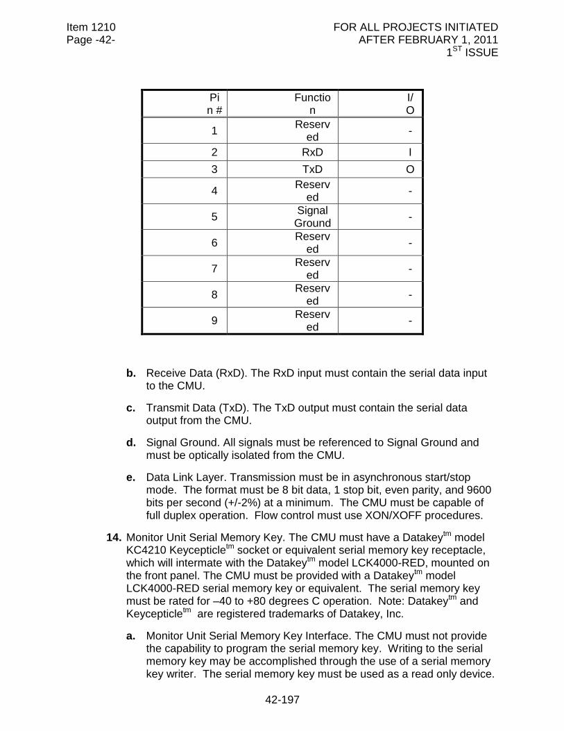
Item 1210 FOR ALL PROJECTS INITIATED Page -42- AFTER FEBRUARY 1, 2011 1ST ISSUE
42-197
b. Receive Data (RxD). The RxD input must contain the serial data input to the CMU.
c. Transmit Data (TxD). The TxD output must contain the serial data output from the CMU.
d. Signal Ground. All signals must be referenced to Signal Ground and must be optically isolated from the CMU.
e. Data Link Layer. Transmission must be in asynchronous start/stop mode. The format must be 8 bit data, 1 stop bit, even parity, and 9600 bits per second (+/-2%) at a minimum. The CMU must be capable of full duplex operation. Flow control must use XON/XOFF procedures.
14. Monitor Unit Serial Memory Key. The CMU must have a Datakeytm model KC4210 Keycepticletm socket or equivalent serial memory key receptacle, which will intermate with the Datakeytm model LCK4000-RED, mounted on the front panel. The CMU must be provided with a Datakeytm model LCK4000-RED serial memory key or equivalent. The serial memory key must be rated for –40 to +80 degrees C operation. Note: Datakeytm and Keycepticletm are registered trademarks of Datakey, Inc.
a. Monitor Unit Serial Memory Key Interface. The CMU must not provide the capability to program the serial memory key. Writing to the serial memory key may be accomplished through the use of a serial memory key writer. The serial memory key must be used as a read only device.
Pin #
Function
I/O
1 Reserv
ed -
2 RxD I
3 TxD O
4 Reserv
ed -
5 Signal
Ground -
6 Reserv
ed -
7 Reserv
ed -
8 Reserv
ed -
9 Reserv
ed -
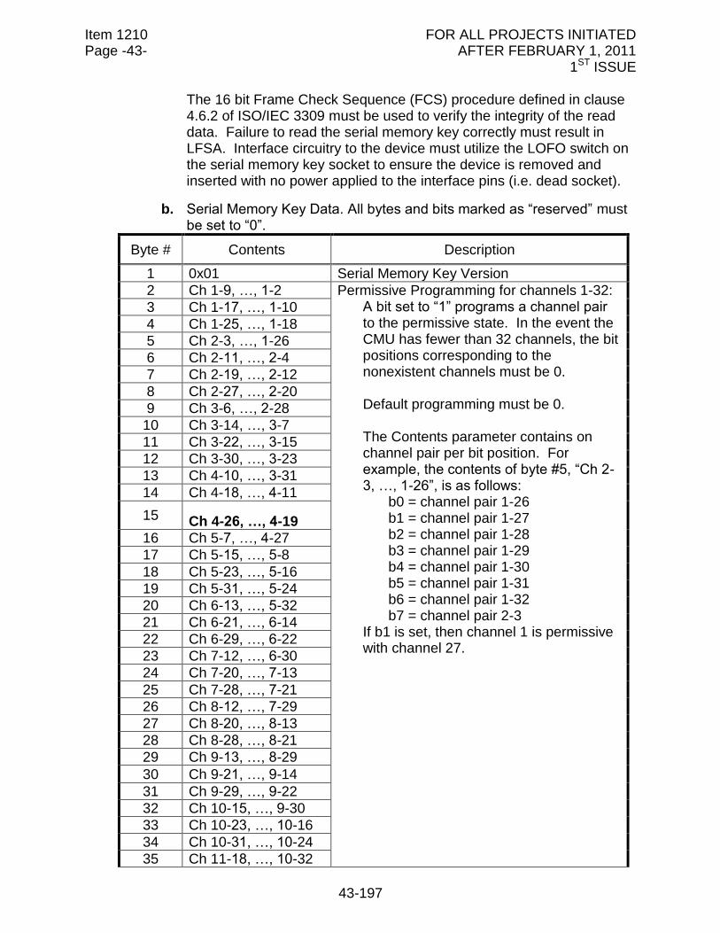
Item 1210 FOR ALL PROJECTS INITIATED Page -43- AFTER FEBRUARY 1, 2011 1ST ISSUE
43-197
The 16 bit Frame Check Sequence (FCS) procedure defined in clause 4.6.2 of ISO/IEC 3309 must be used to verify the integrity of the read data. Failure to read the serial memory key correctly must result in LFSA. Interface circuitry to the device must utilize the LOFO switch on the serial memory key socket to ensure the device is removed and inserted with no power applied to the interface pins (i.e. dead socket).
b. Serial Memory Key Data. All bytes and bits marked as “reserved” must be set to “0”.
Byte # Contents Description
1 0x01 Serial Memory Key Version
2 Ch 1-9, …, 1-2 Permissive Programming for channels 1-32: A bit set to “1” programs a channel pair to the permissive state. In the event the CMU has fewer than 32 channels, the bit positions corresponding to the nonexistent channels must be 0. Default programming must be 0. The Contents parameter contains on channel pair per bit position. For example, the contents of byte #5, “Ch 2-3, …, 1-26”, is as follows:
b0 = channel pair 1-26 b1 = channel pair 1-27 b2 = channel pair 1-28 b3 = channel pair 1-29 b4 = channel pair 1-30 b5 = channel pair 1-31 b6 = channel pair 1-32 b7 = channel pair 2-3
If b1 is set, then channel 1 is permissive with channel 27.
3 Ch 1-17, …, 1-10
4 Ch 1-25, …, 1-18
5 Ch 2-3, …, 1-26
6 Ch 2-11, …, 2-4
7 Ch 2-19, …, 2-12
8 Ch 2-27, …, 2-20
9 Ch 3-6, …, 2-28
10 Ch 3-14, …, 3-7
11 Ch 3-22, …, 3-15
12 Ch 3-30, …, 3-23
13 Ch 4-10, …, 3-31
14 Ch 4-18, …, 4-11
15 Ch 4-26, …, 4-19
16 Ch 5-7, …, 4-27
17 Ch 5-15, …, 5-8
18 Ch 5-23, …, 5-16
19 Ch 5-31, …, 5-24
20 Ch 6-13, …, 5-32
21 Ch 6-21, …, 6-14
22 Ch 6-29, …, 6-22
23 Ch 7-12, …, 6-30
24 Ch 7-20, …, 7-13
25 Ch 7-28, …, 7-21
26 Ch 8-12, …, 7-29
27 Ch 8-20, …, 8-13
28 Ch 8-28, …, 8-21
29 Ch 9-13, …, 8-29
30 Ch 9-21, …, 9-14
31 Ch 9-29, …, 9-22
32 Ch 10-15, …, 9-30
33 Ch 10-23, …, 10-16
34 Ch 10-31, …, 10-24
35 Ch 11-18, …, 10-32
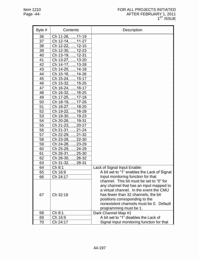
Item 1210 FOR ALL PROJECTS INITIATED Page -44- AFTER FEBRUARY 1, 2011 1ST ISSUE
44-197
Byte # Contents Description
36 Ch 11-26, …, 11-19
37 Ch 12-14, …, 11-27
38 Ch 12-22, …, 12-15
39 Ch 12-30, …, 12-23
40 Ch 13-19, …, 12-31
41 Ch 13-27, …, 13-20
42 Ch 14-17, …, 13-28
43 Ch 14-25, …, 14-18
44 Ch 15-16, …, 14-26
45 Ch 15-24, …, 15-17
46 Ch 15-32, …, 15-25
47 Ch 16-24, …, 16-17
48 Ch 16-32, …, 16-25
49 Ch 17-25, …, 17-18
50 Ch 18-19, …, 17-26
51 Ch 18-27, …, 18-20
52 Ch 19-22, …, 18-28
53 Ch 19-30, …, 19-23
54 Ch 20-26, …, 19-31
55 Ch 21-23, …, 20-27
56 Ch 21-31, …, 21-24
57 Ch 22-29, …, 21-32
58 Ch 23-28, …, 22-30
59 Ch 24-28, …, 23-29
60 Ch 25-29, …, 24-29
61 Ch 26-31, …, 25-30
62 Ch 28-30, …, 26-32
63 Ch 31-32, …, 28-31
64 Ch 8:1 Lack of Signal Input Enable: A bit set to “1” enables the Lack of Signal Input monitoring function for that channel. This bit must be set to “0” for any channel that has an input mapped to a virtual channel. In the event the CMU has fewer than 32 channels, the bit positions corresponding to the nonexistent channels must be 0. Default programming must be 1.
65 Ch 16:9
66 Ch 24:17
67 Ch 32:18
68 Ch 8:1 Dark Channel Map #1 A bit set to “1” disables the Lack of Signal Input monitoring function for that
69 Ch 16:9
70 Ch 24:17
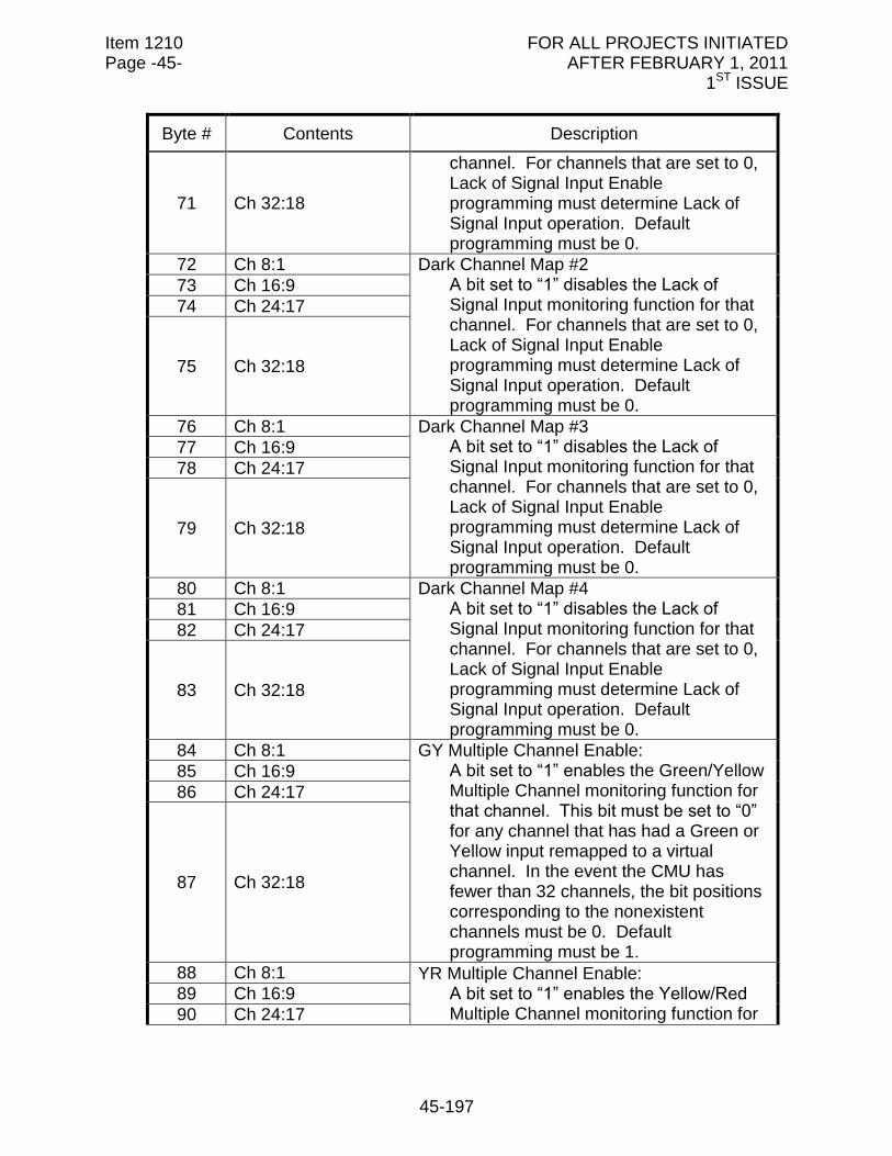
Item 1210 FOR ALL PROJECTS INITIATED Page -45- AFTER FEBRUARY 1, 2011 1ST ISSUE
45-197
Byte # Contents Description
71 Ch 32:18
channel. For channels that are set to 0, Lack of Signal Input Enable programming must determine Lack of Signal Input operation. Default programming must be 0.
72 Ch 8:1 Dark Channel Map #2 A bit set to “1” disables the Lack of Signal Input monitoring function for that channel. For channels that are set to 0, Lack of Signal Input Enable programming must determine Lack of Signal Input operation. Default programming must be 0.
73 Ch 16:9
74 Ch 24:17
75 Ch 32:18
76 Ch 8:1 Dark Channel Map #3 A bit set to “1” disables the Lack of Signal Input monitoring function for that channel. For channels that are set to 0, Lack of Signal Input Enable programming must determine Lack of Signal Input operation. Default programming must be 0.
77 Ch 16:9
78 Ch 24:17
79 Ch 32:18
80 Ch 8:1 Dark Channel Map #4 A bit set to “1” disables the Lack of Signal Input monitoring function for that channel. For channels that are set to 0, Lack of Signal Input Enable programming must determine Lack of Signal Input operation. Default programming must be 0.
81 Ch 16:9
82 Ch 24:17
83 Ch 32:18
84 Ch 8:1 GY Multiple Channel Enable: A bit set to “1” enables the Green/Yellow Multiple Channel monitoring function for that channel. This bit must be set to “0” for any channel that has had a Green or Yellow input remapped to a virtual channel. In the event the CMU has fewer than 32 channels, the bit positions corresponding to the nonexistent channels must be 0. Default programming must be 1.
85 Ch 16:9
86 Ch 24:17
87 Ch 32:18
88 Ch 8:1 YR Multiple Channel Enable: A bit set to “1” enables the Yellow/Red Multiple Channel monitoring function for
89 Ch 16:9
90 Ch 24:17
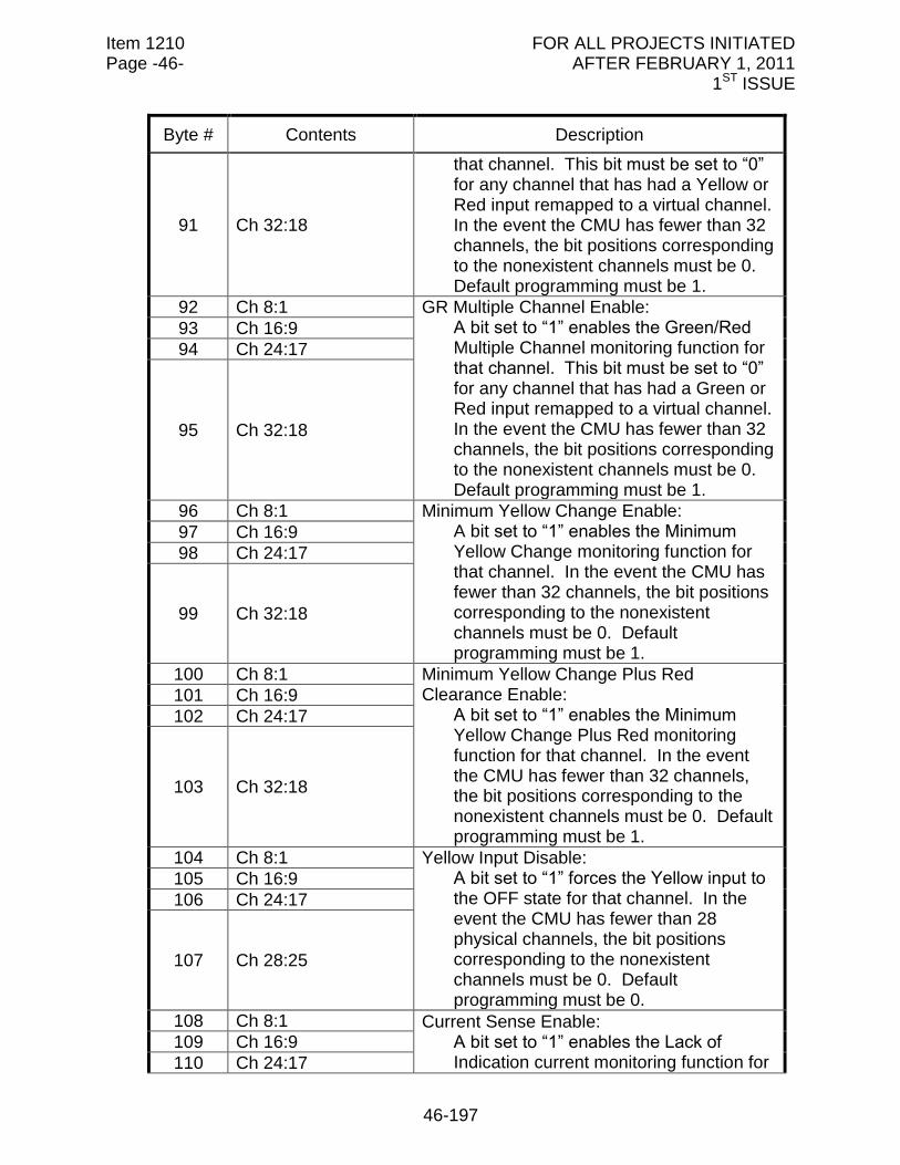
Item 1210 FOR ALL PROJECTS INITIATED Page -46- AFTER FEBRUARY 1, 2011 1ST ISSUE
46-197
Byte # Contents Description
91 Ch 32:18
that channel. This bit must be set to “0” for any channel that has had a Yellow or Red input remapped to a virtual channel. In the event the CMU has fewer than 32 channels, the bit positions corresponding to the nonexistent channels must be 0. Default programming must be 1.
92 Ch 8:1 GR Multiple Channel Enable: A bit set to “1” enables the Green/Red Multiple Channel monitoring function for that channel. This bit must be set to “0” for any channel that has had a Green or Red input remapped to a virtual channel. In the event the CMU has fewer than 32 channels, the bit positions corresponding to the nonexistent channels must be 0. Default programming must be 1.
93 Ch 16:9
94 Ch 24:17
95 Ch 32:18
96 Ch 8:1 Minimum Yellow Change Enable: A bit set to “1” enables the Minimum Yellow Change monitoring function for that channel. In the event the CMU has fewer than 32 channels, the bit positions corresponding to the nonexistent channels must be 0. Default programming must be 1.
97 Ch 16:9
98 Ch 24:17
99 Ch 32:18
100 Ch 8:1 Minimum Yellow Change Plus Red Clearance Enable:
A bit set to “1” enables the Minimum Yellow Change Plus Red monitoring function for that channel. In the event the CMU has fewer than 32 channels, the bit positions corresponding to the nonexistent channels must be 0. Default programming must be 1.
101 Ch 16:9
102 Ch 24:17
103 Ch 32:18
104 Ch 8:1 Yellow Input Disable: A bit set to “1” forces the Yellow input to the OFF state for that channel. In the event the CMU has fewer than 28 physical channels, the bit positions corresponding to the nonexistent channels must be 0. Default programming must be 0.
105 Ch 16:9
106 Ch 24:17
107 Ch 28:25
108 Ch 8:1 Current Sense Enable: A bit set to “1” enables the Lack of Indication current monitoring function for
109 Ch 16:9
110 Ch 24:17
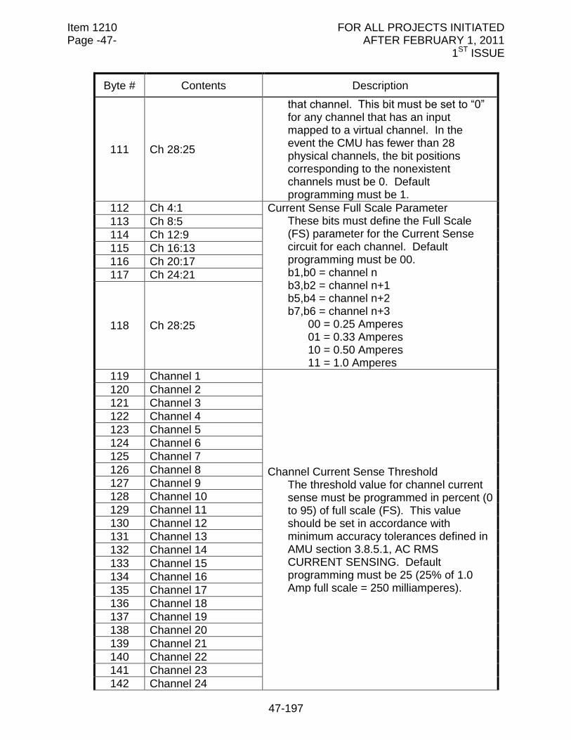
Item 1210 FOR ALL PROJECTS INITIATED Page -47- AFTER FEBRUARY 1, 2011 1ST ISSUE
47-197
Byte # Contents Description
111 Ch 28:25
that channel. This bit must be set to “0” for any channel that has an input mapped to a virtual channel. In the event the CMU has fewer than 28 physical channels, the bit positions corresponding to the nonexistent channels must be 0. Default programming must be 1.
112 Ch 4:1 Current Sense Full Scale Parameter These bits must define the Full Scale (FS) parameter for the Current Sense circuit for each channel. Default programming must be 00. b1,b0 = channel n b3,b2 = channel n+1 b5,b4 = channel n+2 b7,b6 = channel n+3
00 = 0.25 Amperes 01 = 0.33 Amperes 10 = 0.50 Amperes 11 = 1.0 Amperes
113 Ch 8:5
114 Ch 12:9
115 Ch 16:13
116 Ch 20:17
117 Ch 24:21
118 Ch 28:25
119 Channel 1
Channel Current Sense Threshold The threshold value for channel current sense must be programmed in percent (0 to 95) of full scale (FS). This value should be set in accordance with minimum accuracy tolerances defined in AMU section 3.8.5.1, AC RMS CURRENT SENSING. Default programming must be 25 (25% of 1.0 Amp full scale = 250 milliamperes).
120 Channel 2
121 Channel 3
122 Channel 4
123 Channel 5
124 Channel 6
125 Channel 7
126 Channel 8
127 Channel 9
128 Channel 10
129 Channel 11
130 Channel 12
131 Channel 13
132 Channel 14
133 Channel 15
134 Channel 16
135 Channel 17
136 Channel 18
137 Channel 19
138 Channel 20
139 Channel 21
140 Channel 22
141 Channel 23
142 Channel 24
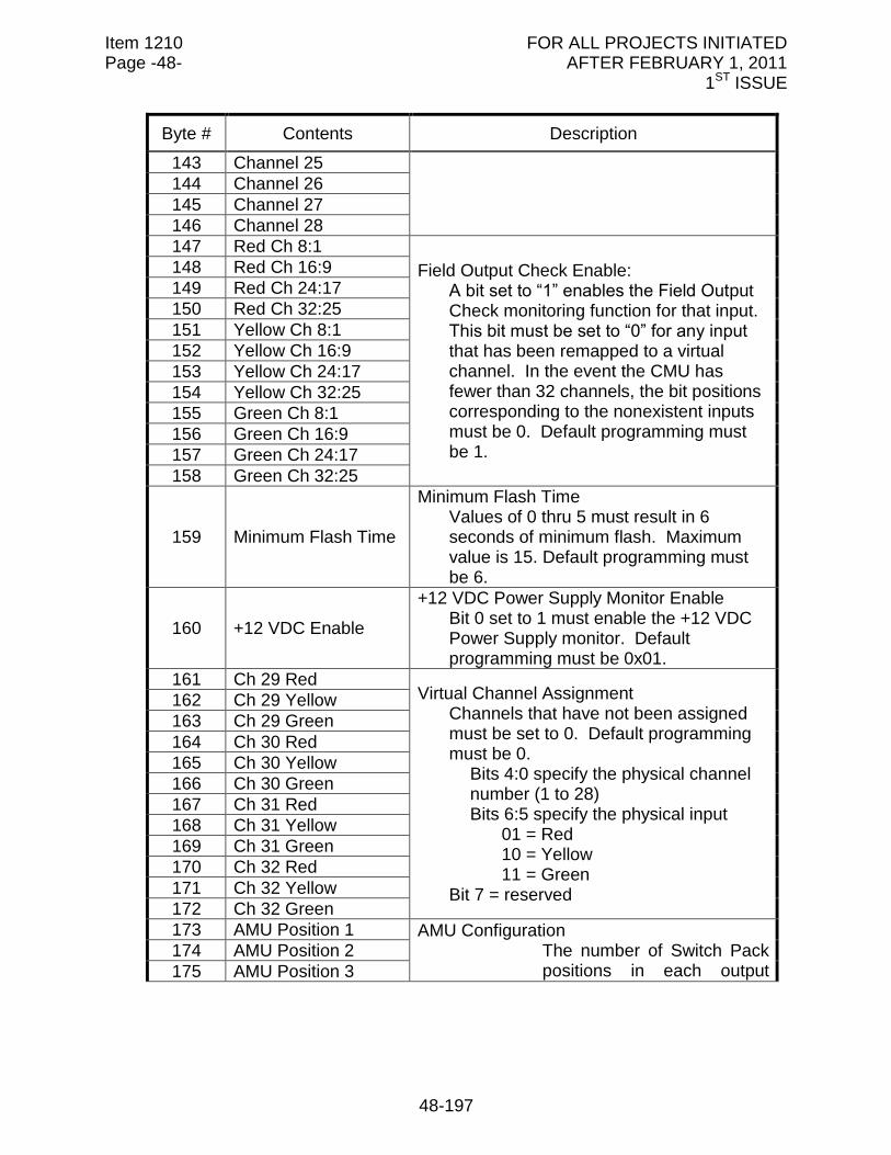
Item 1210 FOR ALL PROJECTS INITIATED Page -48- AFTER FEBRUARY 1, 2011 1ST ISSUE
48-197
Byte # Contents Description
143 Channel 25
144 Channel 26
145 Channel 27
146 Channel 28
147 Red Ch 8:1
Field Output Check Enable: A bit set to “1” enables the Field Output Check monitoring function for that input. This bit must be set to “0” for any input that has been remapped to a virtual channel. In the event the CMU has fewer than 32 channels, the bit positions corresponding to the nonexistent inputs must be 0. Default programming must be 1.
148 Red Ch 16:9
149 Red Ch 24:17
150 Red Ch 32:25
151 Yellow Ch 8:1
152 Yellow Ch 16:9
153 Yellow Ch 24:17
154 Yellow Ch 32:25
155 Green Ch 8:1
156 Green Ch 16:9
157 Green Ch 24:17
158 Green Ch 32:25
159 Minimum Flash Time
Minimum Flash Time Values of 0 thru 5 must result in 6 seconds of minimum flash. Maximum value is 15. Default programming must be 6.
160 +12 VDC Enable
+12 VDC Power Supply Monitor Enable Bit 0 set to 1 must enable the +12 VDC Power Supply monitor. Default programming must be 0x01.
161 Ch 29 Red Virtual Channel Assignment
Channels that have not been assigned must be set to 0. Default programming must be 0.
Bits 4:0 specify the physical channel number (1 to 28) Bits 6:5 specify the physical input
01 = Red 10 = Yellow 11 = Green
Bit 7 = reserved
162 Ch 29 Yellow
163 Ch 29 Green
164 Ch 30 Red
165 Ch 30 Yellow
166 Ch 30 Green
167 Ch 31 Red
168 Ch 31 Yellow
169 Ch 31 Green
170 Ch 32 Red
171 Ch 32 Yellow
172 Ch 32 Green
173 AMU Position 1 AMU Configuration The number of Switch Pack positions in each output
174 AMU Position 2
175 AMU Position 3
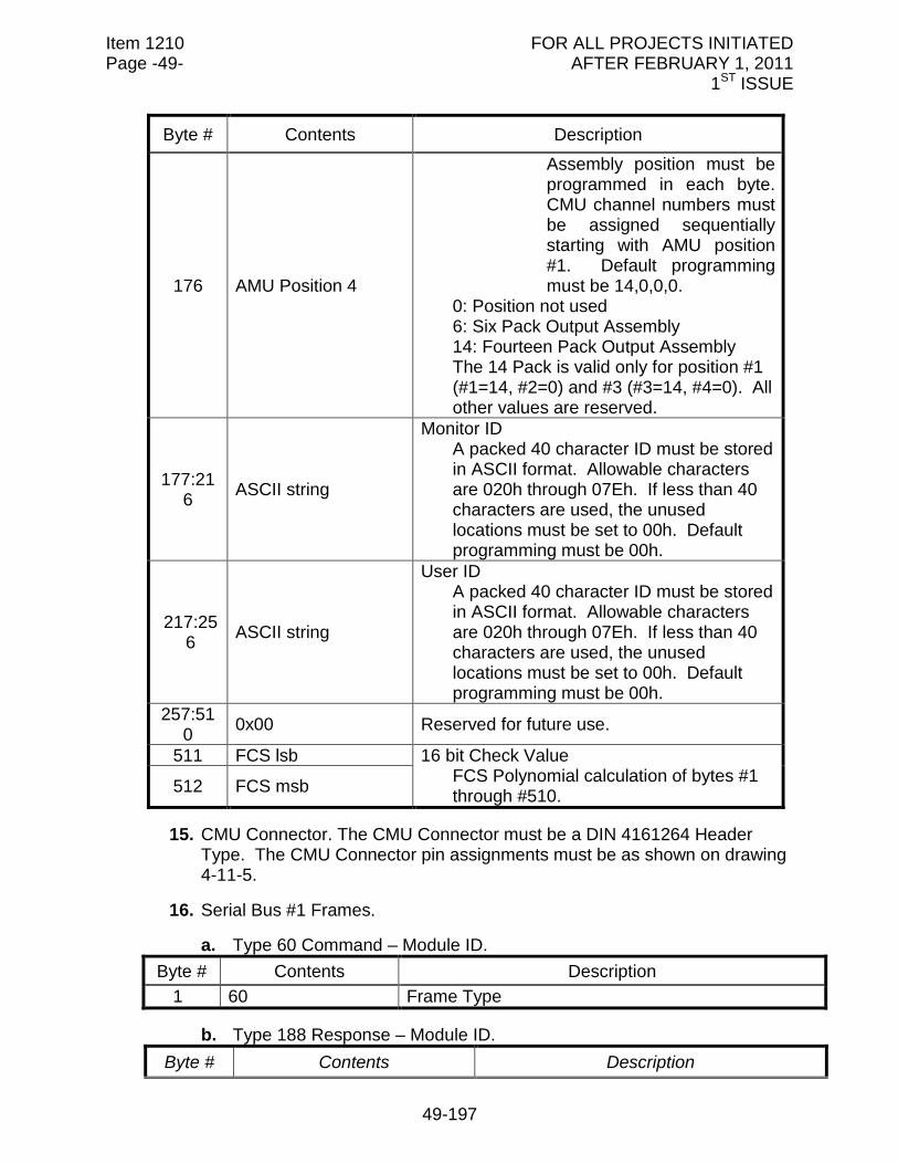
Item 1210 FOR ALL PROJECTS INITIATED Page -49- AFTER FEBRUARY 1, 2011 1ST ISSUE
49-197
Byte # Contents Description
176 AMU Position 4
Assembly position must be programmed in each byte. CMU channel numbers must be assigned sequentially starting with AMU position #1. Default programming must be 14,0,0,0.
0: Position not used 6: Six Pack Output Assembly 14: Fourteen Pack Output Assembly The 14 Pack is valid only for position #1 (#1=14, #2=0) and #3 (#3=14, #4=0). All other values are reserved.
177:216
ASCII string
Monitor ID A packed 40 character ID must be stored in ASCII format. Allowable characters are 020h through 07Eh. If less than 40 characters are used, the unused locations must be set to 00h. Default programming must be 00h.
217:256
ASCII string
User ID A packed 40 character ID must be stored in ASCII format. Allowable characters are 020h through 07Eh. If less than 40 characters are used, the unused locations must be set to 00h. Default programming must be 00h.
257:510
0x00 Reserved for future use.
511 FCS lsb 16 bit Check Value FCS Polynomial calculation of bytes #1 through #510.
512 FCS msb
15. CMU Connector. The CMU Connector must be a DIN 4161264 Header Type. The CMU Connector pin assignments must be as shown on drawing 4-11-5.
16. Serial Bus #1 Frames.
a. Type 60 Command – Module ID.
Byte # Contents Description
1 60 Frame Type
b. Type 188 Response – Module ID.
Byte # Contents Description
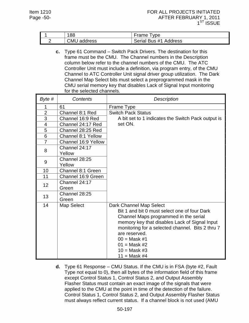
Item 1210 FOR ALL PROJECTS INITIATED Page -50- AFTER FEBRUARY 1, 2011 1ST ISSUE
50-197
1 188 Frame Type
2 CMU address Serial Bus #1 Address
c. Type 61 Command – Switch Pack Drivers. The destination for this frame must be the CMU. The Channel numbers in the Description column below refer to the channel numbers of the CMU. The ATC Controller Unit must include a definition, via program entry, of the CMU Channel to ATC Controller Unit signal driver group utilization. The Dark Channel Map Select bits must select a preprogrammed mask in the CMU serial memory key that disables Lack of Signal Input monitoring for the selected channels.
Byte # Contents Description
1 61 Frame Type
2 Channel 8:1 Red Switch Pack Status A bit set to 1 indicates the Switch Pack output is set ON.
3 Channel 16:9 Red
4 Channel 24:17 Red
5 Channel 28:25 Red
6 Channel 8:1 Yellow
7 Channel 16:9 Yellow
8 Channel 24:17 Yellow
9 Channel 28:25 Yellow
10 Channel 8:1 Green
11 Channel 16:9 Green
12 Channel 24:17 Green
13 Channel 28:25 Green
14 Map Select Dark Channel Map Select Bit 1 and bit 0 must select one of four Dark Channel Maps programmed in the serial memory key that disables Lack of Signal Input monitoring for a selected channel. Bits 2 thru 7 are reserved. 00 = Mask #1 01 = Mask #2 10 = Mask #3 11 = Mask #4
d. Type 61 Response – CMU Status. If the CMU is in FSA (byte #2, Fault Type not equal to 0), then all bytes of the information field of this frame except Control Status 1, Control Status 2, and Output Assembly Flasher Status must contain an exact image of the signals that were applied to the CMU at the point in time of the detection of the failure. Control Status 1, Control Status 2, and Output Assembly Flasher Status must always reflect current status. If a channel block is not used (AMU

Item 1210 FOR ALL PROJECTS INITIATED Page -51- AFTER FEBRUARY 1, 2011 1ST ISSUE
51-197
not present) the Channel Fault Status bits, Channel Input Status bits, and Channel Input Voltage values bits for that block must be set to 0.
Byte # Contents Description
1 189 Frame Type
2 Fault Type
Enumerated fault code 00 = No Fault 01 = CMU/AMU +24 VDC 02 = CMU +12 VDC 03 = Conflict 04 = Serial Bus #1 05 = Serial Bus #3 06 = ATC LFSA Flash (Type 62) 07 = ATC NFSA Flash (Type 62) 08 = Diagnostic 09 = Multiple 10 = Lack of Signal Input 11 = Short Yellow Clearance 12 = Skipped Yellow Clearance 13 = Yellow + Red Clearance 14 = Field Output Check 15 = Serial Memory Key absent 16 = Serial Memory Key FCS error 17 = Serial Memory Key Data error 18 = Local Flash 19 = CB Trip 20 = CMU/AMU AC+ Raw Fail 21 = NRESET Active 22:127 = Reserved 128:255 = Spare
3 Channel Fault Status 8:1 Channel Fault Status Channel Fault Status bits must be set to 1 for channels that were detected in fault for fault types 03, 09, 10, 11, 12, 13, and 14.
4 Channel Fault Status 16:9
5 Channel Fault Status 24:17
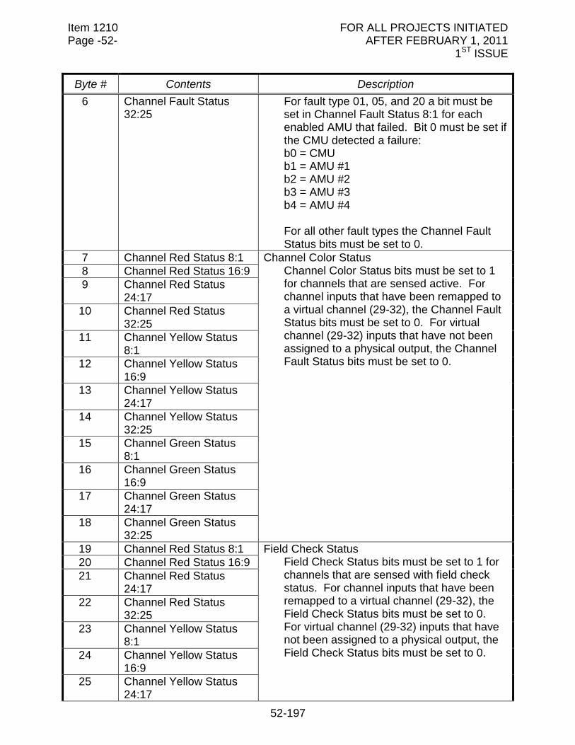
Item 1210 FOR ALL PROJECTS INITIATED Page -52- AFTER FEBRUARY 1, 2011 1ST ISSUE
52-197
Byte # Contents Description
6 Channel Fault Status 32:25
For fault type 01, 05, and 20 a bit must be set in Channel Fault Status 8:1 for each enabled AMU that failed. Bit 0 must be set if the CMU detected a failure: b0 = CMU b1 = AMU #1 b2 = AMU #2 b3 = AMU #3 b4 = AMU #4 For all other fault types the Channel Fault Status bits must be set to 0.
7 Channel Red Status 8:1 Channel Color Status Channel Color Status bits must be set to 1 for channels that are sensed active. For channel inputs that have been remapped to a virtual channel (29-32), the Channel Fault Status bits must be set to 0. For virtual channel (29-32) inputs that have not been assigned to a physical output, the Channel Fault Status bits must be set to 0.
8 Channel Red Status 16:9
9 Channel Red Status 24:17
10 Channel Red Status 32:25
11 Channel Yellow Status 8:1
12 Channel Yellow Status 16:9
13 Channel Yellow Status 24:17
14 Channel Yellow Status 32:25
15 Channel Green Status 8:1
16 Channel Green Status 16:9
17 Channel Green Status 24:17
18 Channel Green Status 32:25
19 Channel Red Status 8:1 Field Check Status Field Check Status bits must be set to 1 for channels that are sensed with field check status. For channel inputs that have been remapped to a virtual channel (29-32), the Field Check Status bits must be set to 0. For virtual channel (29-32) inputs that have not been assigned to a physical output, the Field Check Status bits must be set to 0.
20 Channel Red Status 16:9
21 Channel Red Status 24:17
22 Channel Red Status 32:25
23 Channel Yellow Status 8:1
24 Channel Yellow Status 16:9
25 Channel Yellow Status 24:17
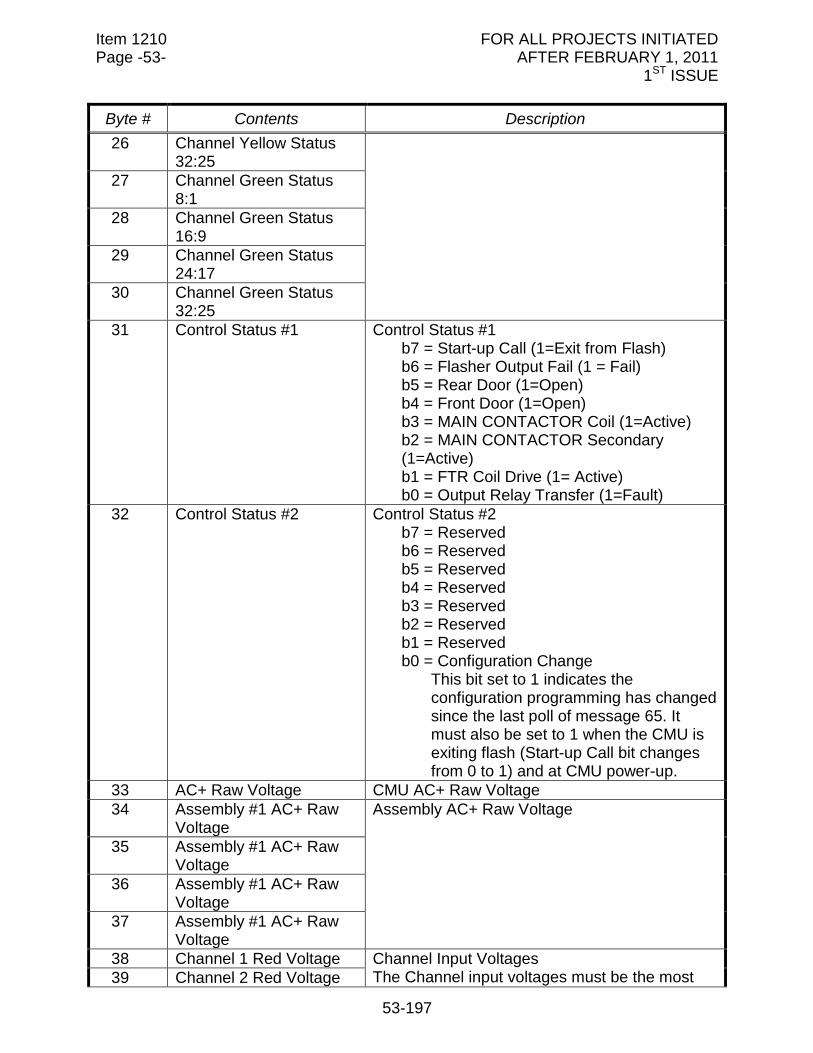
Item 1210 FOR ALL PROJECTS INITIATED Page -53- AFTER FEBRUARY 1, 2011 1ST ISSUE
53-197
Byte # Contents Description
26 Channel Yellow Status 32:25
27 Channel Green Status 8:1
28 Channel Green Status 16:9
29 Channel Green Status 24:17
30 Channel Green Status 32:25
31 Control Status #1 Control Status #1 b7 = Start-up Call (1=Exit from Flash) b6 = Flasher Output Fail (1 = Fail) b5 = Rear Door (1=Open) b4 = Front Door (1=Open) b3 = MAIN CONTACTOR Coil (1=Active) b2 = MAIN CONTACTOR Secondary (1=Active) b1 = FTR Coil Drive (1= Active) b0 = Output Relay Transfer (1=Fault)
32 Control Status #2
Control Status #2 b7 = Reserved b6 = Reserved b5 = Reserved b4 = Reserved b3 = Reserved b2 = Reserved b1 = Reserved b0 = Configuration Change
This bit set to 1 indicates the configuration programming has changed since the last poll of message 65. It must also be set to 1 when the CMU is exiting flash (Start-up Call bit changes from 0 to 1) and at CMU power-up.
33 AC+ Raw Voltage CMU AC+ Raw Voltage
34 Assembly #1 AC+ Raw Voltage
Assembly AC+ Raw Voltage
35 Assembly #1 AC+ Raw Voltage
36 Assembly #1 AC+ Raw Voltage
37 Assembly #1 AC+ Raw Voltage
38 Channel 1 Red Voltage Channel Input Voltages The Channel input voltages must be the most 39 Channel 2 Red Voltage
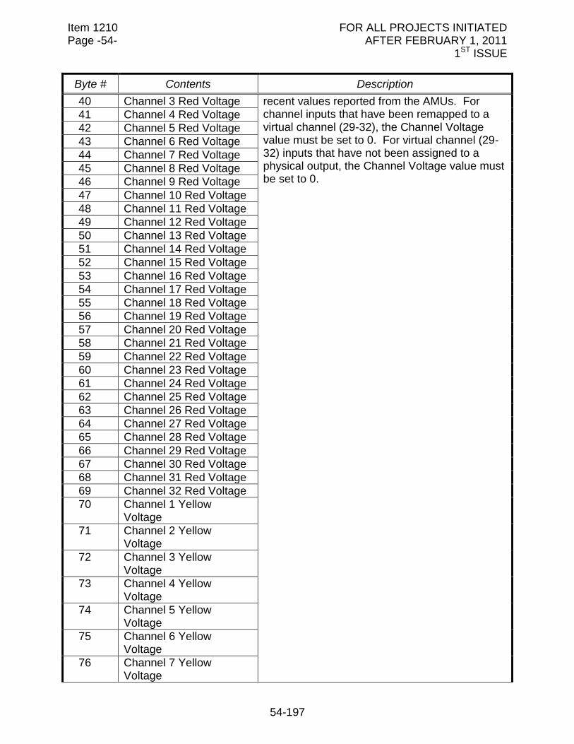
Item 1210 FOR ALL PROJECTS INITIATED Page -54- AFTER FEBRUARY 1, 2011 1ST ISSUE
54-197
Byte # Contents Description
40 Channel 3 Red Voltage recent values reported from the AMUs. For channel inputs that have been remapped to a virtual channel (29-32), the Channel Voltage value must be set to 0. For virtual channel (29-32) inputs that have not been assigned to a physical output, the Channel Voltage value must be set to 0.
41 Channel 4 Red Voltage
42 Channel 5 Red Voltage
43 Channel 6 Red Voltage
44 Channel 7 Red Voltage
45 Channel 8 Red Voltage
46 Channel 9 Red Voltage
47 Channel 10 Red Voltage
48 Channel 11 Red Voltage
49 Channel 12 Red Voltage
50 Channel 13 Red Voltage
51 Channel 14 Red Voltage
52 Channel 15 Red Voltage
53 Channel 16 Red Voltage
54 Channel 17 Red Voltage
55 Channel 18 Red Voltage
56 Channel 19 Red Voltage
57 Channel 20 Red Voltage
58 Channel 21 Red Voltage
59 Channel 22 Red Voltage
60 Channel 23 Red Voltage
61 Channel 24 Red Voltage
62 Channel 25 Red Voltage
63 Channel 26 Red Voltage
64 Channel 27 Red Voltage
65 Channel 28 Red Voltage
66 Channel 29 Red Voltage
67 Channel 30 Red Voltage
68 Channel 31 Red Voltage
69 Channel 32 Red Voltage
70 Channel 1 Yellow Voltage
71 Channel 2 Yellow Voltage
72 Channel 3 Yellow Voltage
73 Channel 4 Yellow Voltage
74 Channel 5 Yellow Voltage
75 Channel 6 Yellow Voltage
76 Channel 7 Yellow Voltage
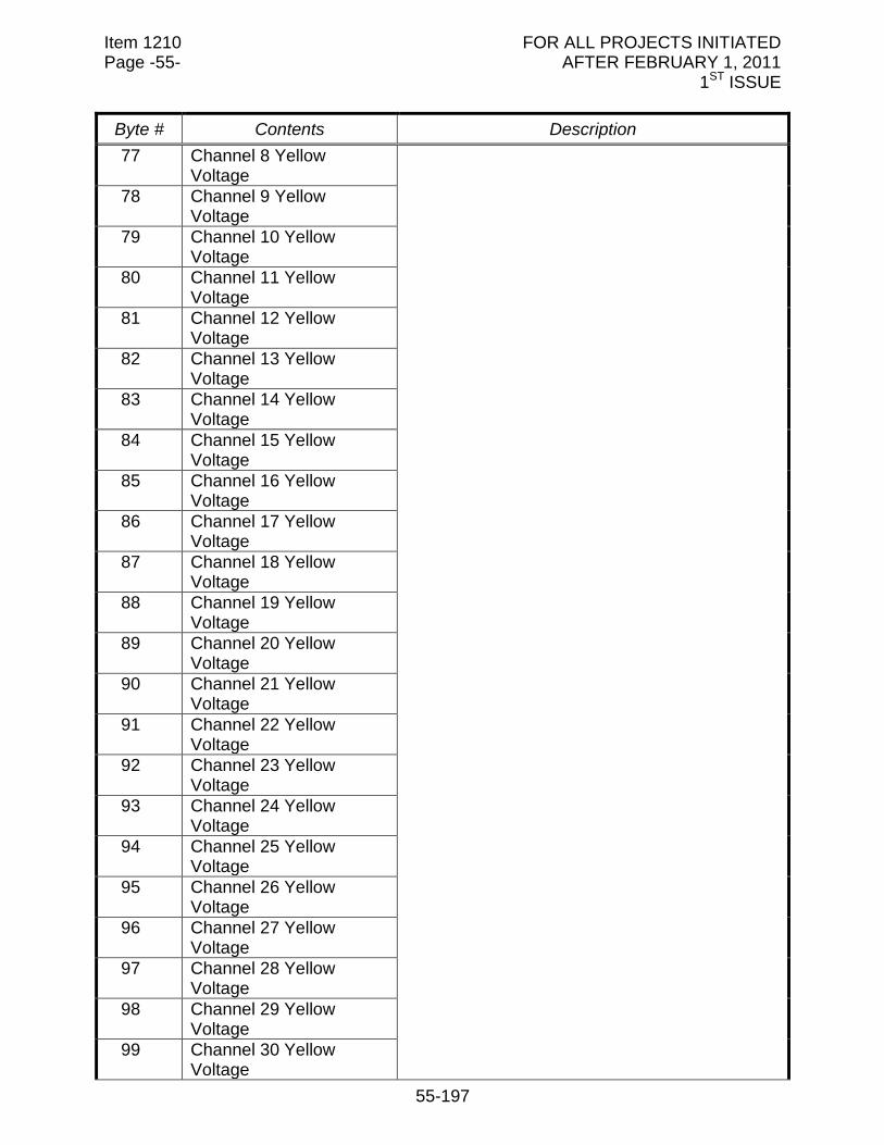
Item 1210 FOR ALL PROJECTS INITIATED Page -55- AFTER FEBRUARY 1, 2011 1ST ISSUE
55-197
Byte # Contents Description
77 Channel 8 Yellow Voltage
78 Channel 9 Yellow Voltage
79 Channel 10 Yellow Voltage
80 Channel 11 Yellow Voltage
81 Channel 12 Yellow Voltage
82 Channel 13 Yellow Voltage
83 Channel 14 Yellow Voltage
84 Channel 15 Yellow Voltage
85 Channel 16 Yellow Voltage
86 Channel 17 Yellow Voltage
87 Channel 18 Yellow Voltage
88 Channel 19 Yellow Voltage
89 Channel 20 Yellow Voltage
90 Channel 21 Yellow Voltage
91 Channel 22 Yellow Voltage
92 Channel 23 Yellow Voltage
93 Channel 24 Yellow Voltage
94 Channel 25 Yellow Voltage
95 Channel 26 Yellow Voltage
96 Channel 27 Yellow Voltage
97 Channel 28 Yellow Voltage
98 Channel 29 Yellow Voltage
99 Channel 30 Yellow Voltage
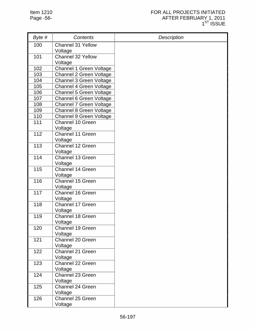
Item 1210 FOR ALL PROJECTS INITIATED Page -56- AFTER FEBRUARY 1, 2011 1ST ISSUE
56-197
Byte # Contents Description
100 Channel 31 Yellow Voltage
101 Channel 32 Yellow Voltage
102 Channel 1 Green Voltage
103 Channel 2 Green Voltage
104 Channel 3 Green Voltage
105 Channel 4 Green Voltage
106 Channel 5 Green Voltage
107 Channel 6 Green Voltage
108 Channel 7 Green Voltage
109 Channel 8 Green Voltage
110 Channel 9 Green Voltage
111 Channel 10 Green Voltage
112 Channel 11 Green Voltage
113 Channel 12 Green Voltage
114 Channel 13 Green Voltage
115 Channel 14 Green Voltage
116 Channel 15 Green Voltage
117 Channel 16 Green Voltage
118 Channel 17 Green Voltage
119 Channel 18 Green Voltage
120 Channel 19 Green Voltage
121 Channel 20 Green Voltage
122 Channel 21 Green Voltage
123 Channel 22 Green Voltage
124 Channel 23 Green Voltage
125 Channel 24 Green Voltage
126 Channel 25 Green Voltage

Item 1210 FOR ALL PROJECTS INITIATED Page -57- AFTER FEBRUARY 1, 2011 1ST ISSUE
57-197
Byte # Contents Description
127 Channel 26 Green Voltage
128 Channel 27 Green Voltage
129 Channel 28 Green Voltage
130 Channel 29 Green Voltage
131 Channel 30 Green Voltage
132 Channel 31 Green Voltage
133 Channel 32 Green Voltage
134 Channel 1 Scaled Channel Load Current The value reported must be the measured current in Amperes times 256 divided by the Full Scale (FS) parameter. For 1 primary turn, FS=10 (range is 0 to 10 Arms) For 2 primary turns, FS=5 (range is 0 to 5 Arms) For 3 primary turns, FS= 3.3 (range is 0 to 3.3 Arms) For 4 primary turns, FS=2.5 (range is 0 to 2.5 Arms)
135 Channel 2
136 Channel 3
137 Channel 4
138 Channel 5
139 Channel 6
140 Channel 7
141 Channel 8
142 Channel 9
143 Channel 10
144 Channel 11
145 Channel 12
146 Channel 13
147 Channel 14
148 Channel 15
149 Channel 16
150 Channel 17
151 Channel 18
152 Channel 19
153 Channel 20
154 Channel 21
155 Channel 22
156 Channel 23
157 Channel 24
158 Channel 25
159 Channel 26
160 Channel 27
161 Channel 28
162 Binary Seconds CMU Time and Date
163 Binary Minutes
164 Binary Hours (0:23)
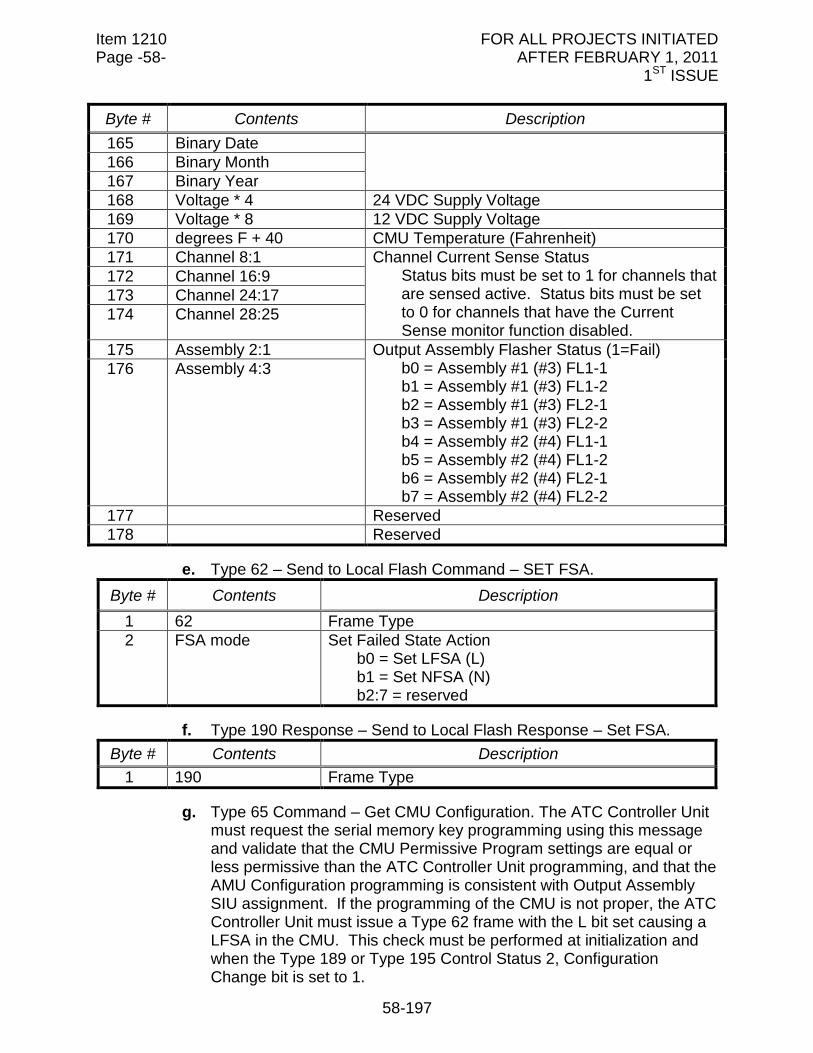
Item 1210 FOR ALL PROJECTS INITIATED Page -58- AFTER FEBRUARY 1, 2011 1ST ISSUE
58-197
Byte # Contents Description
165 Binary Date
166 Binary Month
167 Binary Year
168 Voltage * 4 24 VDC Supply Voltage
169 Voltage * 8 12 VDC Supply Voltage
170 degrees F + 40 CMU Temperature (Fahrenheit)
171 Channel 8:1 Channel Current Sense Status Status bits must be set to 1 for channels that are sensed active. Status bits must be set to 0 for channels that have the Current Sense monitor function disabled.
172 Channel 16:9
173 Channel 24:17
174 Channel 28:25
175 Assembly 2:1 Output Assembly Flasher Status (1=Fail) b0 = Assembly #1 (#3) FL1-1 b1 = Assembly #1 (#3) FL1-2 b2 = Assembly #1 (#3) FL2-1 b3 = Assembly #1 (#3) FL2-2 b4 = Assembly #2 (#4) FL1-1 b5 = Assembly #2 (#4) FL1-2 b6 = Assembly #2 (#4) FL2-1 b7 = Assembly #2 (#4) FL2-2
176 Assembly 4:3
177 Reserved
178 Reserved
e. Type 62 – Send to Local Flash Command – SET FSA.
Byte # Contents Description
1 62 Frame Type
2 FSA mode Set Failed State Action b0 = Set LFSA (L) b1 = Set NFSA (N) b2:7 = reserved
f. Type 190 Response – Send to Local Flash Response – Set FSA.
Byte # Contents Description
1 190 Frame Type
g. Type 65 Command – Get CMU Configuration. The ATC Controller Unit must request the serial memory key programming using this message and validate that the CMU Permissive Program settings are equal or less permissive than the ATC Controller Unit programming, and that the AMU Configuration programming is consistent with Output Assembly SIU assignment. If the programming of the CMU is not proper, the ATC Controller Unit must issue a Type 62 frame with the L bit set causing a LFSA in the CMU. This check must be performed at initialization and when the Type 189 or Type 195 Control Status 2, Configuration Change bit is set to 1.
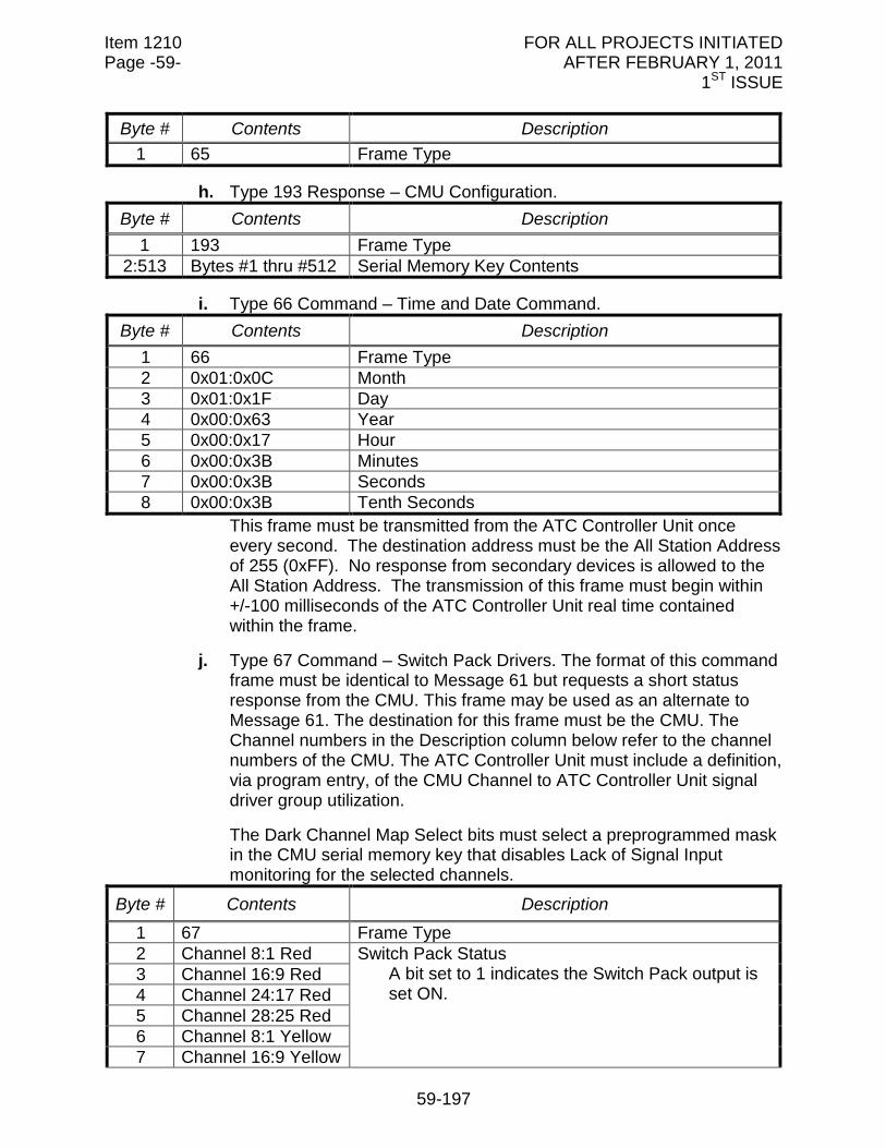
Item 1210 FOR ALL PROJECTS INITIATED Page -59- AFTER FEBRUARY 1, 2011 1ST ISSUE
59-197
Byte # Contents Description
1 65 Frame Type
h. Type 193 Response – CMU Configuration.
Byte # Contents Description
1 193 Frame Type
2:513 Bytes #1 thru #512 Serial Memory Key Contents
i. Type 66 Command – Time and Date Command.
Byte # Contents Description
1 66 Frame Type
2 0x01:0x0C Month
3 0x01:0x1F Day
4 0x00:0x63 Year
5 0x00:0x17 Hour
6 0x00:0x3B Minutes
7 0x00:0x3B Seconds
8 0x00:0x3B Tenth Seconds
This frame must be transmitted from the ATC Controller Unit once every second. The destination address must be the All Station Address of 255 (0xFF). No response from secondary devices is allowed to the All Station Address. The transmission of this frame must begin within +/-100 milliseconds of the ATC Controller Unit real time contained within the frame.
j. Type 67 Command – Switch Pack Drivers. The format of this command frame must be identical to Message 61 but requests a short status response from the CMU. This frame may be used as an alternate to Message 61. The destination for this frame must be the CMU. The Channel numbers in the Description column below refer to the channel numbers of the CMU. The ATC Controller Unit must include a definition, via program entry, of the CMU Channel to ATC Controller Unit signal driver group utilization.
The Dark Channel Map Select bits must select a preprogrammed mask in the CMU serial memory key that disables Lack of Signal Input monitoring for the selected channels.
Byte # Contents Description
1 67 Frame Type
2 Channel 8:1 Red Switch Pack Status A bit set to 1 indicates the Switch Pack output is set ON.
3 Channel 16:9 Red
4 Channel 24:17 Red
5 Channel 28:25 Red
6 Channel 8:1 Yellow
7 Channel 16:9 Yellow
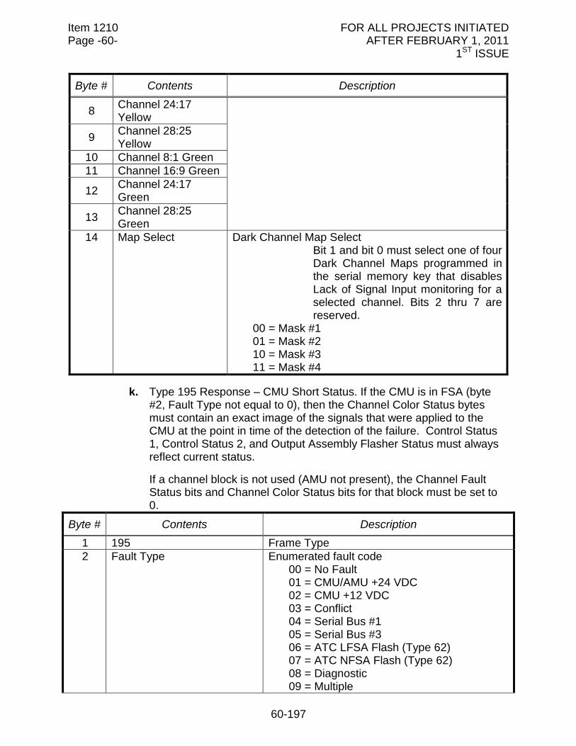
Item 1210 FOR ALL PROJECTS INITIATED Page -60- AFTER FEBRUARY 1, 2011 1ST ISSUE
60-197
Byte # Contents Description
8 Channel 24:17 Yellow
9 Channel 28:25 Yellow
10 Channel 8:1 Green
11 Channel 16:9 Green
12 Channel 24:17 Green
13 Channel 28:25 Green
14 Map Select Dark Channel Map Select Bit 1 and bit 0 must select one of four Dark Channel Maps programmed in the serial memory key that disables Lack of Signal Input monitoring for a selected channel. Bits 2 thru 7 are reserved.
00 = Mask #1 01 = Mask #2 10 = Mask #3 11 = Mask #4
k. Type 195 Response – CMU Short Status. If the CMU is in FSA (byte #2, Fault Type not equal to 0), then the Channel Color Status bytes must contain an exact image of the signals that were applied to the CMU at the point in time of the detection of the failure. Control Status 1, Control Status 2, and Output Assembly Flasher Status must always reflect current status.
If a channel block is not used (AMU not present), the Channel Fault Status bits and Channel Color Status bits for that block must be set to 0.
Byte # Contents Description
1 195 Frame Type
2 Fault Type
Enumerated fault code 00 = No Fault 01 = CMU/AMU +24 VDC 02 = CMU +12 VDC 03 = Conflict 04 = Serial Bus #1 05 = Serial Bus #3 06 = ATC LFSA Flash (Type 62) 07 = ATC NFSA Flash (Type 62) 08 = Diagnostic 09 = Multiple
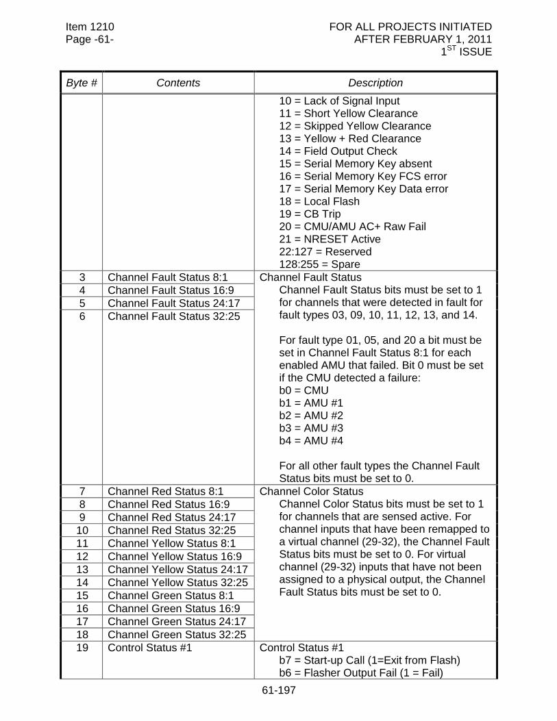
Item 1210 FOR ALL PROJECTS INITIATED Page -61- AFTER FEBRUARY 1, 2011 1ST ISSUE
61-197
Byte # Contents Description
10 = Lack of Signal Input 11 = Short Yellow Clearance 12 = Skipped Yellow Clearance 13 = Yellow + Red Clearance 14 = Field Output Check 15 = Serial Memory Key absent 16 = Serial Memory Key FCS error 17 = Serial Memory Key Data error 18 = Local Flash 19 = CB Trip 20 = CMU/AMU AC+ Raw Fail 21 = NRESET Active 22:127 = Reserved 128:255 = Spare
3 Channel Fault Status 8:1 Channel Fault Status Channel Fault Status bits must be set to 1 for channels that were detected in fault for fault types 03, 09, 10, 11, 12, 13, and 14. For fault type 01, 05, and 20 a bit must be set in Channel Fault Status 8:1 for each enabled AMU that failed. Bit 0 must be set if the CMU detected a failure: b0 = CMU b1 = AMU #1 b2 = AMU #2 b3 = AMU #3 b4 = AMU #4 For all other fault types the Channel Fault Status bits must be set to 0.
4 Channel Fault Status 16:9
5 Channel Fault Status 24:17
6 Channel Fault Status 32:25
7 Channel Red Status 8:1 Channel Color Status Channel Color Status bits must be set to 1 for channels that are sensed active. For channel inputs that have been remapped to a virtual channel (29-32), the Channel Fault Status bits must be set to 0. For virtual channel (29-32) inputs that have not been assigned to a physical output, the Channel Fault Status bits must be set to 0.
8 Channel Red Status 16:9
9 Channel Red Status 24:17
10 Channel Red Status 32:25
11 Channel Yellow Status 8:1
12 Channel Yellow Status 16:9
13 Channel Yellow Status 24:17
14 Channel Yellow Status 32:25
15 Channel Green Status 8:1
16 Channel Green Status 16:9
17 Channel Green Status 24:17
18 Channel Green Status 32:25
19 Control Status #1 Control Status #1 b7 = Start-up Call (1=Exit from Flash) b6 = Flasher Output Fail (1 = Fail)
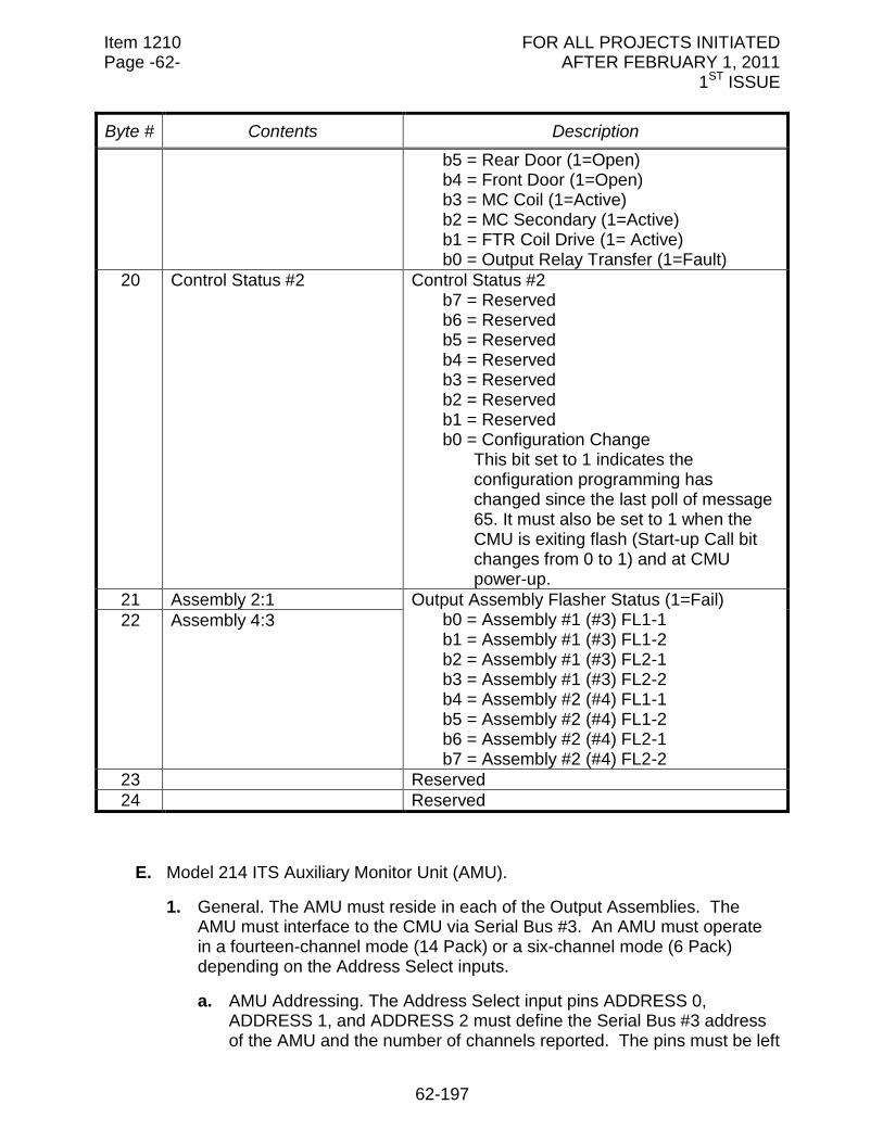
Item 1210 FOR ALL PROJECTS INITIATED Page -62- AFTER FEBRUARY 1, 2011 1ST ISSUE
62-197
Byte # Contents Description
b5 = Rear Door (1=Open) b4 = Front Door (1=Open) b3 = MC Coil (1=Active) b2 = MC Secondary (1=Active) b1 = FTR Coil Drive (1= Active) b0 = Output Relay Transfer (1=Fault)
20 Control Status #2
Control Status #2 b7 = Reserved b6 = Reserved b5 = Reserved b4 = Reserved b3 = Reserved b2 = Reserved b1 = Reserved b0 = Configuration Change
This bit set to 1 indicates the configuration programming has changed since the last poll of message 65. It must also be set to 1 when the CMU is exiting flash (Start-up Call bit changes from 0 to 1) and at CMU power-up.
21 Assembly 2:1 Output Assembly Flasher Status (1=Fail) b0 = Assembly #1 (#3) FL1-1 b1 = Assembly #1 (#3) FL1-2 b2 = Assembly #1 (#3) FL2-1 b3 = Assembly #1 (#3) FL2-2 b4 = Assembly #2 (#4) FL1-1 b5 = Assembly #2 (#4) FL1-2 b6 = Assembly #2 (#4) FL2-1 b7 = Assembly #2 (#4) FL2-2
22 Assembly 4:3
23 Reserved
24 Reserved
E. Model 214 ITS Auxiliary Monitor Unit (AMU).
1. General. The AMU must reside in each of the Output Assemblies. The AMU must interface to the CMU via Serial Bus #3. An AMU must operate in a fourteen-channel mode (14 Pack) or a six-channel mode (6 Pack) depending on the Address Select inputs.
a. AMU Addressing. The Address Select input pins ADDRESS 0, ADDRESS 1, and ADDRESS 2 must define the Serial Bus #3 address of the AMU and the number of channels reported. The pins must be left
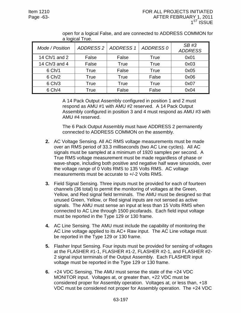
Item 1210 FOR ALL PROJECTS INITIATED Page -63- AFTER FEBRUARY 1, 2011 1ST ISSUE
63-197
open for a logical False, and are connected to ADDRESS COMMON for a logical True.
Mode / Position ADDRESS 2 ADDRESS 1 ADDRESS 0 SB #3
ADDRESS
14 Ch/1 and 2 False False True 0x01
14 Ch/3 and 4 False True True 0x03
6 Ch/1 True False True 0x05
6 Ch/2 True True False 0x06
6 Ch/3 True True True 0x07
6 Ch/4 True False False 0x04
A 14 Pack Output Assembly configured in position 1 and 2 must respond as AMU #1 with AMU #2 reserved. A 14 Pack Output Assembly configured in position 3 and 4 must respond as AMU #3 with AMU #4 reserved.
The 6 Pack Output Assembly must have ADDRESS 2 permanently connected to ADDRESS COMMON on the assembly.
2. AC Voltage Sensing. All AC RMS voltage measurements must be made over an RMS period of 33.3 milliseconds (two AC Line cycles). All AC signals must be sampled at a minimum of 1920 samples per second. A True RMS voltage measurement must be made regardless of phase or wave-shape, including both positive and negative half wave sinusoids, over the voltage range of 0 Volts RMS to 135 Volts RMS. AC voltage measurements must be accurate to +/-2 Volts RMS.
3. Field Signal Sensing. Three inputs must be provided for each of fourteen channels (36 total) to permit the monitoring of voltages at the Green, Yellow, and Red signal field terminals. The AMU must be designed so that unused Green, Yellow, or Red signal inputs are not sensed as active signals. The AMU must sense an input at less than 15 Volts RMS when connected to AC Line through 1500 picofarads. Each field input voltage must be reported in the Type 129 or 130 frame.
4. AC Line Sensing. The AMU must include the capability of monitoring the AC Line voltage applied to its AC+ Raw input. The AC Line voltage must be reported in the Type 129 or 130 frame.
5. Flasher Input Sensing. Four inputs must be provided for sensing of voltages at the FLASHER #1-1, FLASHER #1-2, FLASHER #2-1, and FLASHER #2-2 signal input terminals of the Output Assembly. Each FLASHER input voltage must be reported in the Type 129 or 130 frame.
6. +24 VDC Sensing. The AMU must sense the state of the +24 VDC MONITOR input. Voltages at, or greater than, +22 VDC must be considered proper for Assembly operation. Voltages at, or less than, +18 VDC must be considered not proper for Assembly operation. The +24 VDC
Item 1210 FOR ALL PROJECTS INITIATED Page -64- AFTER FEBRUARY 1, 2011 1ST ISSUE
64-197
MONITOR state must be reported in the Type 129 or 130 frames. The +24 VDC MONITOR voltage section must be electrically isolated from the AC- Raw referenced circuitry.
7. Current Sensing.
a. AC RMS Current Sensing. All AC RMS current measurements must be made over a period of two AC Line cycles (33.3 milliseconds). A True RMS current measurement must be made regardless of phase or wave-shape, including both positive and negative half wave sinusoids. AC current measurements must be accurate to +/-35%.
b. Switch Pack Current Sensing. The AMU must sense the total output current of each Switch Pack. Each Switch Pack output current must be reported in the Type 129 or 130 frames.
The input impedance of the COIL+ input with respect to the COIL-input must be 1000 Ohms. Full-scale current is set by the number of primary turns through the transformer and must be a maximum of four turns. Unless specified otherwise, one turn must be provided.
c. Current Transformer Parameters. The Switch Pack current sensing transformers must meet the following requirements: Linearity 25% from 10 milliamperes to 1Ampere (single
primary turn) Accuracy +/-25% (Rin = 1000 Ohms) Primary Current 10 Amperes maximum Minimum hole size 0.25 in. diameter Insulation Resistance 100 Megohms at 500 VDC The transformer must output a voltage of 1.0 Volts RMS (+/-5%) across 1K Ohms when driven by 1.0 Arms sinusoidal current through one primary turn. Sufficient secondary turns must be provided to compensate for differences in core material and losses to produce the 1.0 Volts RMS output.
8. Diagnostic Error. The AMU must be provided with a resident series of self-check diagnostic capabilities. At a minimum, the AMU must contain provisions to verify all memory elements on power-up and Reset. When an error is detected, the AMU must illuminate the DIAGNOSTIC indicator and disable the Serial Bus #3 port.
a. RAM Diagnostic. This test must verify that all RAM elements are operating correctly at power-up. Patterns must be written to RAM. Each Write must be followed by a Read to verify that it contains the written pattern.
b. Nonvolatile Memory Diagnostic. This test must verify that the nonvolatile ROM(s) contain the proper program. The routine must
Item 1210 FOR ALL PROJECTS INITIATED Page -65- AFTER FEBRUARY 1, 2011 1ST ISSUE
65-197
perform a check on each ROM and make a comparison with a preprogrammed check value. This test must be performed at power-up and at a minimum rate of 1024 bits per second during operation.
c. Internal MPU Monitor. The AMU must monitor the operation of its microprocessor. At a minimum, the monitoring circuit must be triggered at least every 100 milliseconds. The microprocessor must be reset and the DIAGNOSTIC indicator illuminated if the monitoring circuit has not been triggered for a maximum of 1000 milliseconds.
9. Power Requirements. The AMU must generate its own power supply voltage from the AC+ Raw input using no more than 5 Watts. It must be capable of insertion and removal while AC power is applied to the cabinet. Surge current on AC+ Raw input must be less than 2 Amperes peak.
a. Operating Voltage Range. The AMU must be operational over the voltage range of 80 Volts RMS to 135 Volts RMS. The AMU must be fully functional within 500 milliseconds following AC+ Raw voltage exceeding 80 Volts RMS or Reset.
b. Power Supply Holdup. During the loss of AC+ Raw voltage for 700 milliseconds or less the AMU must continue to operate.
10. AMU User Interface. All indicators must be clear LEDS. Clear LEDs must not depend on a reflector or diffusion as part of its design. Clear LEDs must only show the die and not appear to be ON when exposed to ambient light. The following indicators must be provided (Top to Bottom).
a. AC Power Indicator. A green POWER indicator must be provided. The indicator must be illuminated when the AC+ Raw input is 80 Volts RMS (+/-2 Volts RMS) or greater. This indicator must be labeled POWER.
b. Serial Bus #3 Indicator. A yellow Serial Bus #3 indicator must be provided. The indicator must pulse ON for 40 milliseconds each time the AMU correctly receives a frame with its address on the Bus #3 input. This indicator must be labeled SB #3 RX.
c. Diagnostic Indicator. A red DIAGNOSTIC indicator must be provided. The indicator must be ON when an internal diagnostic error is detected. This indicator must be labeled DIAGNOSTIC.
d. Reset Button. A recessed RESET switch must be provided which applies a direct reset to the microprocessor device on the AMU. All voltage and current data must be initialized to 0 following Reset. The access hole must be 0.25 in. in diameter.
e. AMU Connector. The AMU connector must be a DIN 4161296 Header Type. Pins A31 (Equipment Ground), B32 (AC-Raw), and C32 (AC-Raw) must pre-mate before all other pins. The AMU pin assignments must be as shown on drawing 4-11-6.
Item 1210 FOR ALL PROJECTS INITIATED Page -66- AFTER FEBRUARY 1, 2011 1ST ISSUE
66-197
11. Bus #3 Profile.
a. Electrical. TxD+, TxD- and RxD+, RxD- must consist of two interface links conforming to the requirements of the Electronic Industries Association EIA-485, Standard for Electrical Characteristics of Generators and Receivers for use in Balanced Digital Multipoint Systems, dated April 1983. Where differences occur between the EIA-485 standard and this document, this document must govern.
All voltage potentials on the Bus #3 TxD+, TxD-, RxD+, and RxD- interface links must be referenced to AC- Raw.
b. Data Link Layer. The data link layer protocol is based on a subset of HDLC as defined by ISO/IEC 3309. Each frame must consist of the following fields:
(1) Flag byte = 0x7E
(2) Address byte = 0x01 through 0x07
(3) Control byte = 0x13 (U Format)
(4) Information field = defined below in section, Frame Types
(5) Frame Check Sequence = 16 bit FCS procedure defined in clause 4.6.2 of ISO/IEC 3309.
(6) Flag byte = 0x7E
Transmission must be in start/stop mode with basic transparency defined by clause 4.5.2.2 of ISO/IEC 3309 applied. The format must be 8 bit data, 1 stop bit, no parity, and 153,600 bits per second (+/-2%). Only asynchronous half duplex operation must be permitted.
c. Procedures. Frames transmitted by the CMU must be referred to as command frames and frames transmitted by the AMU must be referred to as response frames. Command frames must be transmitted only to those AMUs that are present, as determined by the programming entries made in the CMU. Response frames must only be transmitted as a result of correctly receiving a command frame. The first eight bits in each information field must contain the frame Type number. There must be a maximum of 64 different command frame types and 64 different response frame types. Additionally, there must be 64 different command frame types reserved for special application use and 64 different response frame types reserved for special application use, as outlined below. FRAME TYPES FUNCTION
1-63 Command frame defined by this standard 0, 64-127 Command frame reserved 128-191 Response frame defined by this standard
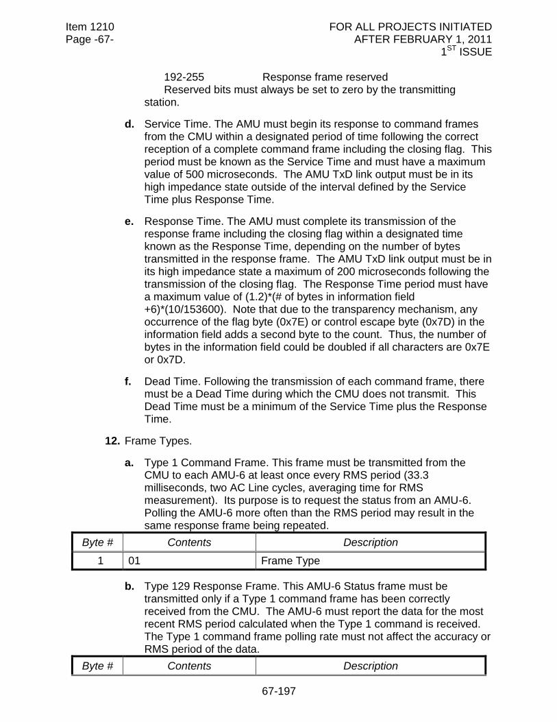
Item 1210 FOR ALL PROJECTS INITIATED Page -67- AFTER FEBRUARY 1, 2011 1ST ISSUE
67-197
192-255 Response frame reserved Reserved bits must always be set to zero by the transmitting
station.
d. Service Time. The AMU must begin its response to command frames from the CMU within a designated period of time following the correct reception of a complete command frame including the closing flag. This period must be known as the Service Time and must have a maximum value of 500 microseconds. The AMU TxD link output must be in its high impedance state outside of the interval defined by the Service Time plus Response Time.
e. Response Time. The AMU must complete its transmission of the response frame including the closing flag within a designated time known as the Response Time, depending on the number of bytes transmitted in the response frame. The AMU TxD link output must be in its high impedance state a maximum of 200 microseconds following the transmission of the closing flag. The Response Time period must have a maximum value of (1.2)*(# of bytes in information field +6)*(10/153600). Note that due to the transparency mechanism, any occurrence of the flag byte (0x7E) or control escape byte (0x7D) in the information field adds a second byte to the count. Thus, the number of bytes in the information field could be doubled if all characters are 0x7E or 0x7D.
f. Dead Time. Following the transmission of each command frame, there must be a Dead Time during which the CMU does not transmit. This Dead Time must be a minimum of the Service Time plus the Response Time.
12. Frame Types.
a. Type 1 Command Frame. This frame must be transmitted from the CMU to each AMU-6 at least once every RMS period (33.3 milliseconds, two AC Line cycles, averaging time for RMS measurement). Its purpose is to request the status from an AMU-6. Polling the AMU-6 more often than the RMS period may result in the same response frame being repeated.
Byte # Contents Description
1 01 Frame Type
b. Type 129 Response Frame. This AMU-6 Status frame must be transmitted only if a Type 1 command frame has been correctly received from the CMU. The AMU-6 must report the data for the most recent RMS period calculated when the Type 1 command is received. The Type 1 command frame polling rate must not affect the accuracy or RMS period of the data.
Byte # Contents Description
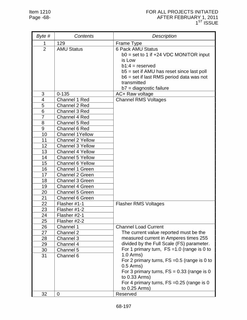
Item 1210 FOR ALL PROJECTS INITIATED Page -68- AFTER FEBRUARY 1, 2011 1ST ISSUE
68-197
Byte # Contents Description
1 129 Frame Type
2 AMU Status 6 Pack AMU Status b0 = set to 1 if +24 VDC MONITOR input is Low b1:4 = reserved b5 = set if AMU has reset since last poll b6 = set if last RMS period data was not transmitted b7 = diagnostic failure
3 0-135 AC+ Raw voltage
4 Channel 1 Red Channel RMS Voltages
5 Channel 2 Red
6 Channel 3 Red
7 Channel 4 Red
8 Channel 5 Red
9 Channel 6 Red
10 Channel 1Yellow
11 Channel 2 Yellow
12 Channel 3 Yellow
13 Channel 4 Yellow
14 Channel 5 Yellow
15 Channel 6 Yellow
16 Channel 1 Green
17 Channel 2 Green
18 Channel 3 Green
19 Channel 4 Green
20 Channel 5 Green
21 Channel 6 Green
22 Flasher #1-1 Flasher RMS Voltages
23 Flasher #1-2
24 Flasher #2-1
25 Flasher #2-2
26 Channel 1 Channel Load Current The current value reported must be the measured current in Amperes times 255 divided by the Full Scale (FS) parameter. For 1 primary turn, FS =1.0 (range is 0 to 1.0 Arms) For 2 primary turns, FS =0.5 (range is 0 to 0.5 Arms) For 3 primary turns, FS = 0.33 (range is 0 to 0.33 Arms) For 4 primary turns, FS =0.25 (range is 0 to 0.25 Arms)
27 Channel 2
28 Channel 3
29 Channel 4
30 Channel 5
31 Channel 6
32 0 Reserved
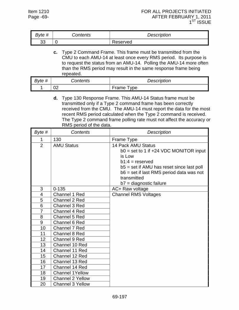
Item 1210 FOR ALL PROJECTS INITIATED Page -69- AFTER FEBRUARY 1, 2011 1ST ISSUE
69-197
Byte # Contents Description
33 0 Reserved
c. Type 2 Command Frame. This frame must be transmitted from the CMU to each AMU-14 at least once every RMS period. Its purpose is to request the status from an AMU-14. Polling the AMU-14 more often than the RMS period may result in the same response frame being repeated.
Byte # Contents Description
1 02 Frame Type
d. Type 130 Response Frame. This AMU-14 Status frame must be transmitted only if a Type 2 command frame has been correctly received from the CMU. The AMU-14 must report the data for the most recent RMS period calculated when the Type 2 command is received. The Type 2 command frame polling rate must not affect the accuracy or RMS period of the data.
Byte # Contents Description
1 130 Frame Type
2 AMU Status 14 Pack AMU Status b0 = set to 1 if +24 VDC MONITOR input is Low b1:4 = reserved b5 = set if AMU has reset since last poll b6 = set if last RMS period data was not transmitted b7 = diagnostic failure
3 0-135 AC+ Raw voltage
4 Channel 1 Red Channel RMS Voltages
5 Channel 2 Red
6 Channel 3 Red
7 Channel 4 Red
8 Channel 5 Red
9 Channel 6 Red
10 Channel 7 Red
11 Channel 8 Red
12 Channel 9 Red
13 Channel 10 Red
14 Channel 11 Red
15 Channel 12 Red
16 Channel 13 Red
17 Channel 14 Red
18 Channel 1Yellow
19 Channel 2 Yellow
20 Channel 3 Yellow
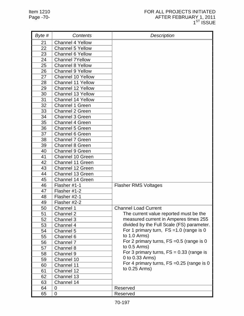
Item 1210 FOR ALL PROJECTS INITIATED Page -70- AFTER FEBRUARY 1, 2011 1ST ISSUE
70-197
Byte # Contents Description
21 Channel 4 Yellow
22 Channel 5 Yellow
23 Channel 6 Yellow
24 Channel 7Yellow
25 Channel 8 Yellow
26 Channel 9 Yellow
27 Channel 10 Yellow
28 Channel 11 Yellow
29 Channel 12 Yellow
30 Channel 13 Yellow
31 Channel 14 Yellow
32 Channel 1 Green
33 Channel 2 Green
34 Channel 3 Green
35 Channel 4 Green
36 Channel 5 Green
37 Channel 6 Green
38 Channel 7 Green
39 Channel 8 Green
40 Channel 9 Green
41 Channel 10 Green
42 Channel 11 Green
43 Channel 12 Green
44 Channel 13 Green
45 Channel 14 Green
46 Flasher #1-1 Flasher RMS Voltages
47 Flasher #1-2
48 Flasher #2-1
49 Flasher #2-2
50 Channel 1 Channel Load Current The current value reported must be the measured current in Amperes times 255 divided by the Full Scale (FS) parameter. For 1 primary turn, FS =1.0 (range is 0 to 1.0 Arms) For 2 primary turns, FS =0.5 (range is 0 to 0.5 Arms) For 3 primary turns, FS = 0.33 (range is 0 to 0.33 Arms) For 4 primary turns, FS =0.25 (range is 0 to 0.25 Arms)
51 Channel 2
52 Channel 3
53 Channel 4
54 Channel 5
55 Channel 6
56 Channel 7
57 Channel 8
58 Channel 9
59 Channel 10
60 Channel 11
61 Channel 12
62 Channel 13
63 Channel 14
64 0 Reserved
65 0 Reserved
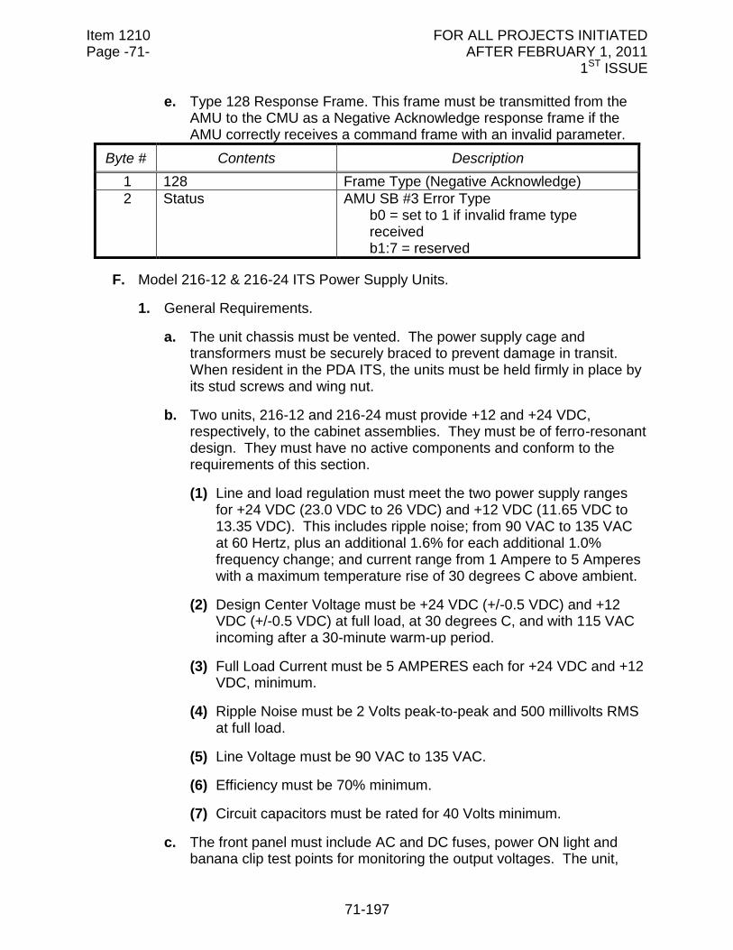
Item 1210 FOR ALL PROJECTS INITIATED Page -71- AFTER FEBRUARY 1, 2011 1ST ISSUE
71-197
e. Type 128 Response Frame. This frame must be transmitted from the AMU to the CMU as a Negative Acknowledge response frame if the AMU correctly receives a command frame with an invalid parameter.
Byte # Contents Description
1 128 Frame Type (Negative Acknowledge)
2 Status AMU SB #3 Error Type b0 = set to 1 if invalid frame type received b1:7 = reserved
F. Model 216-12 & 216-24 ITS Power Supply Units.
1. General Requirements.
a. The unit chassis must be vented. The power supply cage and transformers must be securely braced to prevent damage in transit. When resident in the PDA ITS, the units must be held firmly in place by its stud screws and wing nut.
b. Two units, 216-12 and 216-24 must provide +12 and +24 VDC, respectively, to the cabinet assemblies. They must be of ferro-resonant design. They must have no active components and conform to the requirements of this section.
(1) Line and load regulation must meet the two power supply ranges for +24 VDC (23.0 VDC to 26 VDC) and +12 VDC (11.65 VDC to 13.35 VDC). This includes ripple noise; from 90 VAC to 135 VAC at 60 Hertz, plus an additional 1.6% for each additional 1.0% frequency change; and current range from 1 Ampere to 5 Amperes with a maximum temperature rise of 30 degrees C above ambient.
(2) Design Center Voltage must be +24 VDC (+/-0.5 VDC) and +12 VDC (+/-0.5 VDC) at full load, at 30 degrees C, and with 115 VAC incoming after a 30-minute warm-up period.
(3) Full Load Current must be 5 AMPERES each for +24 VDC and +12 VDC, minimum.
(4) Ripple Noise must be 2 Volts peak-to-peak and 500 millivolts RMS at full load.
(5) Line Voltage must be 90 VAC to 135 VAC.
(6) Efficiency must be 70% minimum.
(7) Circuit capacitors must be rated for 40 Volts minimum.
c. The front panel must include AC and DC fuses, power ON light and banana clip test points for monitoring the output voltages. The unit,
Item 1210 FOR ALL PROJECTS INITIATED Page -72- AFTER FEBRUARY 1, 2011 1ST ISSUE
72-197
including terminals, must be protected with a 1K Ohm, 0.5 watt, resister to prevent accidental contact with energized parts.
G. Type 218 – Serial Interface Unit (SIU).
1. General. The SIU must be capable of processing fifty-four Input/Output pins and four Optical Input pins. When installed in an ITS Input Assembly, it processes twenty-four detector outputs (pins F and W), twenty-four detector status outputs, and provides six detector rest signals (per two slots). In advanced detectors, the status outputs may be converted to per channel resets. When installed in an ITS 14 Pack Output Assembly, the SIU controls fourteen Switch Pack Units (forty-two Outputs) and four Optical Inputs through the CDC socket.
2. Power Requirements. The SIU requires a nominal supply voltage of 24 VDC (+/-2 VDC). A voltage of 16 VDC or less must be considered loss of power and a voltage of 18 VDC or greater must be considered adequate for operation. The SIU must not require more than 300 milliamperes over the voltage range of 16 VDC to 30 VDC and the power surge must be limited to a maximum of 1.25 Amperes from initial application of DC power. The SIU must not be damaged by insertion to, or removal from, powered input or output assemblies. The SIU operates normally for 700 milliseconds after power loss.
3. Microprocessor. The SIU Controller Unit must include a microprocessor/controller unit together with all required clocking and support circuitry.
4. Memory. Operational software necessary to meet housekeeping and functional requirements must be provided resident in socketed firmware or internal Flash memory.
5. Control Signals. The SIU uses NRESET lines for SIU shut down/turn on operations matching the ATC Controller Unit CPU. The SIU must be fully initialized and providing specified operation upon NRESET Line going HIGH (Power Up). In the ATC Controller, the NRESET operation must cause the SIU program restart. No prior message operation data retention is required. The Request Module Status Response may report this restart as either a Power On or Watchdog. ATC Controller Unit LINESYNC is used as a system time reference. The microprocessor/controller unit is reset by any of the following:
Pushbutton Reset
NRESET Signal
+5 VDC out of regulation
Microprocessor/controller unit watchdog
6. Time Reference. The SIU includes a 1 Kilohertz Time Reference to provide system response time stamps. The 1 Kilohertz Time Reference must maintain a frequency accuracy of +/-0.01% (+/-0.1 counts per second).
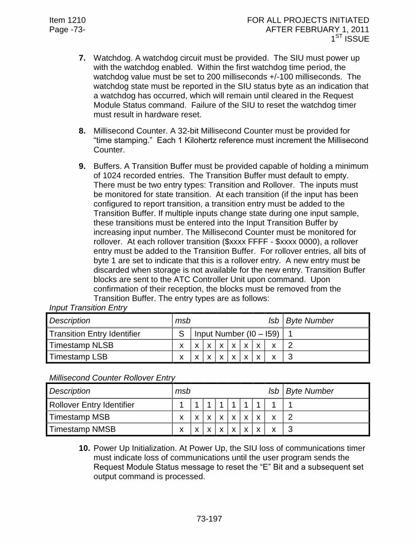
Item 1210 FOR ALL PROJECTS INITIATED Page -73- AFTER FEBRUARY 1, 2011 1ST ISSUE
73-197
7. Watchdog. A watchdog circuit must be provided. The SIU must power up with the watchdog enabled. Within the first watchdog time period, the watchdog value must be set to 200 milliseconds +/-100 milliseconds. The watchdog state must be reported in the SIU status byte as an indication that a watchdog has occurred, which will remain until cleared in the Request Module Status command. Failure of the SIU to reset the watchdog timer must result in hardware reset.
8. Millisecond Counter. A 32-bit Millisecond Counter must be provided for “time stamping.” Each 1 Kilohertz reference must increment the Millisecond Counter.
9. Buffers. A Transition Buffer must be provided capable of holding a minimum of 1024 recorded entries. The Transition Buffer must default to empty. There must be two entry types: Transition and Rollover. The inputs must be monitored for state transition. At each transition (if the input has been configured to report transition, a transition entry must be added to the Transition Buffer. If multiple inputs change state during one input sample, these transitions must be entered into the Input Transition Buffer by increasing input number. The Millisecond Counter must be monitored for rollover. At each rollover transition ($xxxx FFFF - $xxxx 0000), a rollover entry must be added to the Transition Buffer. For rollover entries, all bits of byte 1 are set to indicate that this is a rollover entry. A new entry must be discarded when storage is not available for the new entry. Transition Buffer blocks are sent to the ATC Controller Unit upon command. Upon confirmation of their reception, the blocks must be removed from the Transition Buffer. The entry types are as follows:
Input Transition Entry
Description msb lsb Byte Number
Transition Entry Identifier S Input Number (I0 – I59) 1
Timestamp NLSB x x x x x x x x 2
Timestamp LSB x x x x x x x x 3
Millisecond Counter Rollover Entry
Description msb lsb Byte Number
Rollover Entry Identifier 1 1 1 1 1 1 1 1 1
Timestamp MSB x x x x x x x x 2
Timestamp NMSB x x x x x x x x 3
10. Power Up Initialization. At Power Up, the SIU loss of communications timer must indicate loss of communications until the user program sends the Request Module Status message to reset the “E” Bit and a subsequent set output command is processed.
Item 1210 FOR ALL PROJECTS INITIATED Page -74- AFTER FEBRUARY 1, 2011 1ST ISSUE
74-197
11. Interrupts. All interrupts must be capable of asynchronous operation with respect to all processing and all other interrupts. The SIU includes three interrupt sources as follows:
a. MILLISECOND Interrupt. MILLISECOND Interrupt must be activated by the Time Reference. A timestamp rollover flag set by Millisecond Counter (MC) rollover must be cleared only on command.
b. LINESYNC Interrupt. The LINESYNC signal must be generated by the controller power supply. LINESYNC Interrupt must be generated by both the 0-1 and 1-0 transitions of the LINESYNC signal. The LINESYNC interrupt must monitor the Millisecond Counter interrupt and set the Millisecond Counter error flag if there has not been an interrupt
from the 1 Kilohertz source for 0.5 seconds (60 consecutive LINESYNC interrupts). The LINESYNC interrupt must synchronize the 1 KHz time reference with the 0-1 transition of the LINESYNC signal once a second. A LINESYNC error flag must be set if the LINESYNC
interrupt has not successfully executed for 0.5 seconds or longer (500 consecutive millisecond interrupts).
c. Line Frequency Reference. The Line Frequency Reference input pin must receive a square wave signal from the cabinet power supply for the purposes of synchronizing SIU outputs with the AC line. Line Frequency Reference Interrupt must be generated by both the 0-1 and 1-0 transitions of the Line Frequency Reference signal. The Line Frequency Reference interrupt must monitor the Millisecond Counter interrupt and set the Millisecond Counter error flag if there has not been
an interrupt from the 1 Kilohertz source for 0.5 seconds (60 consecutive Line Frequency Reference interrupts). The Line Frequency Reference interrupt must synchronize the Time Reference with the 0-1 transition of the Line Frequency Reference signal once a second. A Line Frequency Reference error flag must be set if the Line Frequency Reference interrupt has not successfully executed for 0.5
seconds or longer (500 consecutive millisecond interrupts). The electrical characteristics of the Line Frequency input are as follows:
(1) A voltage between 0 and 8 volts must be considered the LOW state, and must occur when the AC line is in the positive half cycle.
(2) A voltage between 16 and 26 volts must be considered the High state, and must occur when the AC line is in the negative half-cycle.
(3) The Line Frequency Reference input must exhibit a nominal impedance of 10K (+/-10%) to the +24 VDC input and must not have more than 1000 picofarads of load capacitance.
(4) The rise and fall time of the signal connected to this input must not exceed 50 microseconds.
Item 1210 FOR ALL PROJECTS INITIATED Page -75- AFTER FEBRUARY 1, 2011 1ST ISSUE
75-197
The SIU/BIU input must be used by the SIU to determine the AC timing source. If the SIU/BIU input is grounded, LINESYNC must be used as the interrupt source. If the SIU/BIU input is pulled up, Line Frequency Reference must be used as the interrupt source.
d. Communication Service Routine. A low-level communication service routine must be provided to handle reception, transmission, and EIA-485 communication faults. The communication server must automatically:
For Transmission: Generate the opening and closing flags Generate the CRC value Generate the abort sequence (minimum of 8 consecutive ‘1’ bits) when commanded by the Microprocessor Unit Provide zero bit insertion
For Reception: Detect the opening and closing flags
Provide address comparison, generating an interrupt for messages addressed to the SIU, and ignoring messages not addressed to the SIU Strip out inserted zeros Calculate the CRC value, compare it to the received value, and generate an interrupt on an error Generate an interrupt if an abort sequence is received
12. Communication Processing. The task must be to process the command messages received from the ATC Controller Unit, prepare, and start response transmission. The response message transmission must begin within 4 milliseconds of the receipt of the received message. The SIU must complete the execution of each command within 70 milliseconds of the end of each response message transmission.
13. Input Processing. This task must process the raw input data scanned in by the 1 milliseconds interrupt routine, perform all filtering, and maintain the transition queue entries.
14. Inputs and Outputs. The SIU must have four Optically Coupled Inputs, fifty-four Parallel Input/Outputs and four Serial Ports.
a. Optically-Coupled Inputs.
(1) Opto Common. The Opto Common input must be the common reference pin for four Opto Inputs.
(2) Opto Inputs. The Opto Inputs are intended to provide optical isolation for Pedestrian Detection, internal cabinet functions, Remote Interconnect or other auxiliary inputs. The Opto Inputs are intended to connect through external 27K Ohm, 1-Watt resistors for
Item 1210 FOR ALL PROJECTS INITIATED Page -76- AFTER FEBRUARY 1, 2011 1ST ISSUE
76-197
120 VAC operations, and are intended for direct connection to 12 VAC for Pedestrian Detector applications. These inputs may also be used for low-true DC applications when the Opto Common pin is connected to -24 VDC. These inputs may function in the place of 242/252 isolator modules.
(a) The Opto Inputs must provide electrical isolation of 10 Megohms minimum resistance and 1000 VAC RMS minimum breakdown to all connector pins except the Opto Common pin, at a maximum breakdown leakage current of 1 milliamperes RMS.
(b) These inputs must exhibit nominal impedance to the Opto Common pin of 5000 Ohms, +10% to the Opto Common input.
(c) The Opto Inputs must not recognize 3 Volts RMS (AC sinusoid or DC) or less relative to the Opto Common input.
(d) The Opto Inputs must recognize 8 Volts RMS (AC sinusoid or DC) or more relative to the Opto Common input.
(e) Any steady state voltage applied between an Opto Input and the Opto Common must not exceed 35 VAC RMS.
(f) Opto Inputs must not be acknowledged when active for 25 milliseconds or less, and must be acknowledged when active for 50 milliseconds or more.
The first Output Assembly assignments must be dedicated as follows:
PIN 1st OUTPUT ASSEMBLY APPLICABLE HOUSING TYPE Opto Input 1 Manual Control Enable All Opto Input 2 Interval Advance All Opto Input 3 Stop Time All Opto Input 4 Manual Flash All
Opto Input Common AC- All
b. Parallel Inputs and Outputs. SIU must control fifty-four input/output lines using ground-true logic.
(1) Input Section. Each input must be read logic "1" (ON) when the input voltage at its field connector input is less than 8 VDC, and must be read logic "0" (OFF) when the input voltage exceeds 16 VDC. Each input must have an internal pull-up to +24 VDC of 11K Ohms maximum, and must not deliver greater than 10 milliamperes to a short circuit to ground.
Item 1210 FOR ALL PROJECTS INITIATED Page -77- AFTER FEBRUARY 1, 2011 1ST ISSUE
77-197
(2) Output Section. Each output written as a logic "1" (ON) must have a voltage at its field connector output of less than 4.0 VDC. Each output written as logic "0" (OFF) must provide an open circuit (1 Megohm or more) at its field connector output. Each output must consist of an open-collector capable of driving 40 VDC minimum and sinking 100 milliamperes minimum. Each output circuit must be capable of switching from logic "1" to logic "0" within 100 microseconds when connected to a load of 100K Ohms minimum. Each output circuit must be protected from transients of 10 microseconds (+/-2 microseconds) duration, +/-300 VDC from a 1K Ohm source, with a maximum rate of 1 pulse per second. Each output must latch the data written and remain stable until either new data is written or the active-low reset signal. Upon an active-low reset signal, each output must latch a logic "0" and retain that state until a new writing. The state of all output circuits at the time of Power Up or in Power Down state must be OFF. It must be possible to simultaneously assert all outputs within 100 microseconds of each other. An output circuit state not changed during a new writing must not glitch when other output circuits are updated.
(3) Input/Output Function. Each parallel Input/Output function contains all of the functions listed below of both the Input Function and Output Function.
(4) Input Section Function. Input scanning must begin at I0 (bit 0) and proceed to the highest numbered input, ascending from LSB to MSB. Each complete input scan must finish within 100 microseconds. Once sampled, the logic state of an input must be held until the next input scan. Each input must be sampled 1,000 times per second. The time interval between samples must be 1 milliseconds (+/-100 microseconds). The Millisecond Counter must be sampled within 10 microseconds of the completion of the input scan.
(5) Input Data Filtering. If configured, the inputs must be filtered by the SIU to remove signal bounce. The filtered input signals must then be monitored for changes as noted. The filtering parameters for each input must consist of Ignore Input Flag and the ON and OFF filter samples. If the Ignore Input flag is set, no input transition entries must be placed into the Input Transition buffer. The ON and OFF filter samples must determine the number of consecutive samples an input must be ON and OFF, respectively, before a change of state is recognized. If the change of state is shorter than the specified value, the change of state must be ignored. The ON and OFF filter values must be in the range of 0 to 255. A filter value of 0, for either or both values, must result in no filtering for this input. The default values for input signals after reset must be as follows:
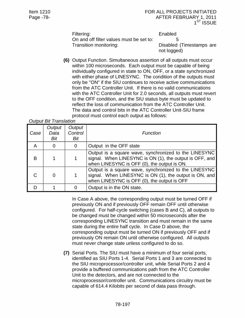
Item 1210 FOR ALL PROJECTS INITIATED Page -78- AFTER FEBRUARY 1, 2011 1ST ISSUE
78-197
Filtering: Enabled On and off filter values must be set to: 5 Transition monitoring: Disabled (Timestamps are
not logged)
(6) Output Function. Simultaneous assertion of all outputs must occur within 100 microseconds. Each output must be capable of being individually configured in state to ON, OFF, or a state synchronized with either phase of LINESYNC. The condition of the outputs must only be "ON" if the SIU continues to receive active communications from the ATC Controller Unit. If there is no valid communications with the ATC Controller Unit for 2.0 seconds, all outputs must revert to the OFF condition, and the SIU status byte must be updated to reflect the loss of communication from the ATC Controller Unit. The data and control bits in the ATC Controller Unit-SIU frame protocol must control each output as follows:
Output Bit Translation
Case
Output Data Bit
Output Control
Bit
Function
A 0 0 Output in the OFF state
B 1 1 Output is a square wave, synchronized to the LINESYNC signal. When LINESYNC is ON (1), the output is OFF, and when LINESYNC is OFF (0), the output is ON.
C 0 1 Output is a square wave, synchronized to the LINESYNC signal. When LINESYNC is ON (1), the output is ON, and when LINESYNC is OFF (0), the output is OFF
D 1 0 Output is in the ON state.
In Case A above, the corresponding output must be turned OFF if previously ON and if previously OFF remain OFF until otherwise configured. For half-cycle switching (cases B and C), all outputs to be changed must be changed within 50 microseconds after the corresponding LINESYNC transition and must remain in the same state during the entire half cycle. In Case D above, the corresponding output must be turned ON if previously OFF and if previously ON remain ON until otherwise configured. All outputs must never change state unless configured to do so.
(7) Serial Ports. The SIU must have a minimum of four serial ports, identified as SIU Ports 1-4. Serial Ports 1 and 3 are connected to the SIU microprocessor/controller unit, while Serial Ports 2 and 4 provide a buffered communications path from the ATC Controller Unit to the detectors, and are not connected to the microprocessor/controller unit. Communications circuitry must be capable of 614.4 Kilobits per second of data pass through.
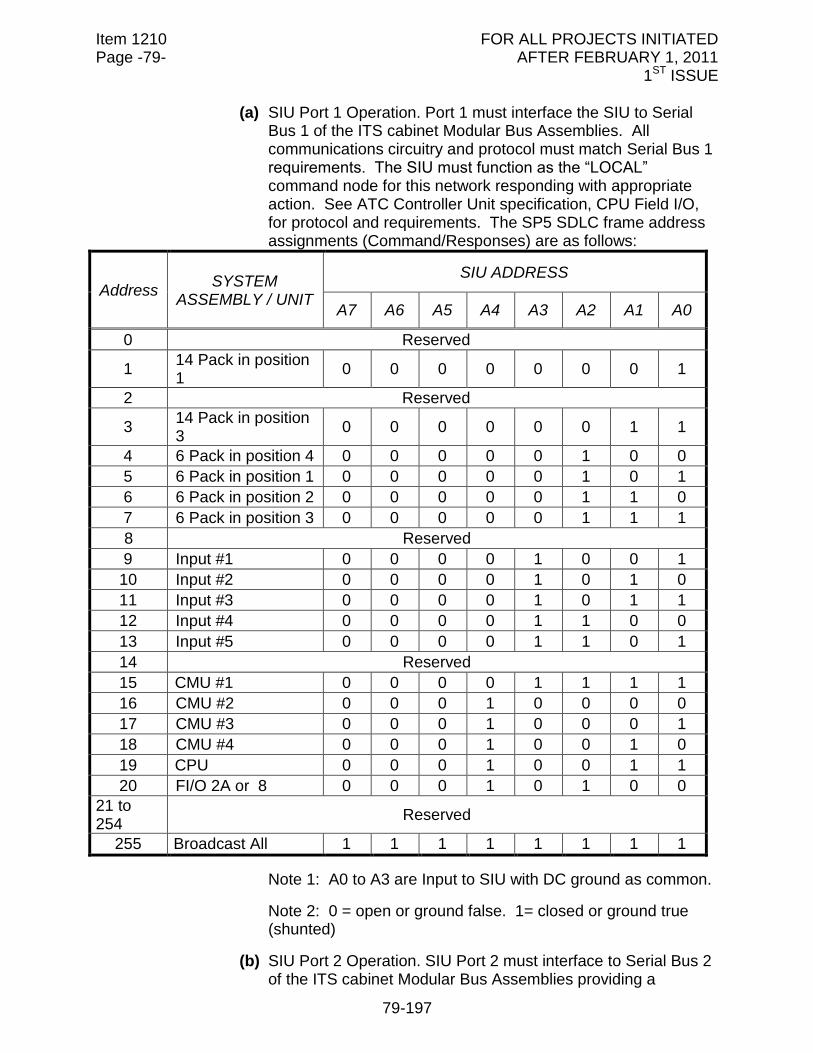
Item 1210 FOR ALL PROJECTS INITIATED Page -79- AFTER FEBRUARY 1, 2011 1ST ISSUE
79-197
(a) SIU Port 1 Operation. Port 1 must interface the SIU to Serial Bus 1 of the ITS cabinet Modular Bus Assemblies. All communications circuitry and protocol must match Serial Bus 1 requirements. The SIU must function as the “LOCAL” command node for this network responding with appropriate action. See ATC Controller Unit specification, CPU Field I/O, for protocol and requirements. The SP5 SDLC frame address assignments (Command/Responses) are as follows:
Address SYSTEM
ASSEMBLY / UNIT
SIU ADDRESS
A7 A6 A5 A4 A3 A2 A1 A0
0 Reserved
1 14 Pack in position 1
0 0 0 0 0 0 0 1
2 Reserved
3 14 Pack in position 3
0 0 0 0 0 0 1 1
4 6 Pack in position 4 0 0 0 0 0 1 0 0
5 6 Pack in position 1 0 0 0 0 0 1 0 1
6 6 Pack in position 2 0 0 0 0 0 1 1 0
7 6 Pack in position 3 0 0 0 0 0 1 1 1
8 Reserved
9 Input #1 0 0 0 0 1 0 0 1
10 Input #2 0 0 0 0 1 0 1 0
11 Input #3 0 0 0 0 1 0 1 1
12 Input #4 0 0 0 0 1 1 0 0
13 Input #5 0 0 0 0 1 1 0 1
14 Reserved
15 CMU #1 0 0 0 0 1 1 1 1
16 CMU #2 0 0 0 1 0 0 0 0
17 CMU #3 0 0 0 1 0 0 0 1
18 CMU #4 0 0 0 1 0 0 1 0
19 CPU 0 0 0 1 0 0 1 1
20 FI/O 2A or 8 0 0 0 1 0 1 0 0
21 to 254
Reserved
255 Broadcast All 1 1 1 1 1 1 1 1
Note 1: A0 to A3 are Input to SIU with DC ground as common.
Note 2: 0 = open or ground false. 1= closed or ground true (shunted)
(b) SIU Port 2 Operation. SIU Port 2 must interface to Serial Bus 2 of the ITS cabinet Modular Bus Assemblies providing a
Item 1210 FOR ALL PROJECTS INITIATED Page -80- AFTER FEBRUARY 1, 2011 1ST ISSUE
80-197
communications path to the ATC Controller Unit for block data retrieval. No connection exists between SIU Port 1 and SIU Port 2. Similarly, no connection exists between SIU Port 2 and the microprocessor/controller unit. All data transfers between SIU Ports 1 and 2 must be accomplished by the ATC Controller Unit. For example, data sent back may include monitor diagnostic status and communication status; input diagnostics status (detector sensor or isolator); and processed channel inputs data such as rate counts, occupancies, average speeds, speed classification and incident/presence.
Synchronous Operation. If the ATC Controller Unit is communicating via Logical Port SP3S, SIU Port 2 must communicate in SDLC format and protocol, and the hardware requirements must match Serial Bus 2 (synchronous TX/RX using TxC from the ATC Controller Unit CPU for common clocking).
Asynchronous Operation. If the ATC Controller Unit is communicating via Logical Port SP3, SIU Port 2 must communicate in an asynchronous START BIT/STOP BIT format and protocol.
SIU Port 3 Operation. The SIU Port 3 must be provided for communication to a personal computer via a front panel 9-position subminiature D-type connector and EIA-232 logic. Its purpose is to upload diagnostic information, and to download the SIU program. The SIU Port 3 protocol must be defined by the vendor, and operate with vendor-supplied software. The pin assignments of SIU Port 3 must match that of ATC Controller Unit C60 port.
SIU Port 4 Operation. SIU Port 4 consists of Detector Rack signal INBUS TxD, INBUS RxD, INBUS TxC, and INBUS RxC, and must conform to the electrical standards of EIA-485, single-ended. In this scheme, the RxD- and RxC- inputs of the EIA-485 receivers are connected to 2.5 Volts, while the TxD- and TxC- outputs of the EIA-485 drivers are not used. SIU Port 4 receivers must withstand +/-25 Volts, suitable for reception of EIA-232 bipolar signals. All four INBUS signals must be terminated at each receiver with impedance of 6,800 Ohms (+/-5%), connected from signal to +5V Ground on the SIU. The detector vendor must define the SIU Port 4 messages. The detector vendor must define the SIU Port 4 protocol. The SIU provides one inversion to ensure a controller MARK equates to a detector MARK. The SIU must provide an LED indicator for TxD and RxD, such that is illuminated during a MARK (START Bit, for example) and extinguished during a SPACE (STOP Bit, for example). SIU Port 4 provides the
Item 1210 FOR ALL PROJECTS INITIATED Page -81- AFTER FEBRUARY 1, 2011 1ST ISSUE
81-197
buffering to SIU Port 2, allowing the ATC Controller Unit to communicate directly to the detectors, as follows:
Synchronous Operation. If the ATC Controller Unit is communicating to detectors via Logical Port SP3S, the SIU Port 4 buffers must convert SIU Port 2 TxD+ and TxD- to EIA-485 which must then be transmitted to the detectors via INBUS TxD. Likewise, the SIU Port 4 buffers must convert SIU Port 2 TxC+ and TxC- to EIA-485, which must then be transmitted to the detectors via INBUS TxC.
If the ATC Controller Unit is communicating to detectors via Logical Port SP3S, the SIU Port 4 buffers must convert INBUS RxD from EIA-485, which must then be transmitted to the ATC Controller Unit via SIU Port 2 RxD+ and RxD-. Likewise, the SIU Port 4 buffers must convert INBUS RxC from EIA-485, which must then be transmitted to the ATC Controller Unit via SIU Port 2 RxC+ and RxC-.
Asynchronous Operation. If the ATC Controller Unit is communicating to detectors via Logical Port SP3, the SIU Port 4 buffers must convert SIU Port 2 TxD+ and TxD- to EIA-485 which must be transmitted to the detectors via INBUS TxD.
If the ATC Controller Unit is communicating to detectors via Logical Port SP3, the SIU Port 4 buffers must convert INBUS RxD is from EIA-485, which must be transmitted to the ATC Controller Unit via SIU Port 2 RxD+ and RxD-.
Asynchronous operation must not use Port 2 TxC+, TxC-, RxC+, RxC-, nor Port 4 INBUS TxC, or INBUS RxC.
Assembly Address Output. The SIU must sense the rack address block and generate a square wave on the ASSEMBLY ADDRESS signal as follows:
ASSEMBLY ADDRESS ASSEMBLY ADDRESS FREQUENCY (Hertz)(+/-
15%)
1 60 2 30 3 15 4 7.5 5 3.75
INBUS RTS Input. The INBUS RTS line must be pulled to +24 Volts via a 10K Ohm resistor on the SIU. In systems using legacy detectors that do not use INBUS RTS, this line must not be used (no connection). Detectors equipped with INBUS RTS
Item 1210 FOR ALL PROJECTS INITIATED Page -82- AFTER FEBRUARY 1, 2011 1ST ISSUE
82-197
must drive this line low when transmitting data from that detector to the SIU via INBUS. When not transmitting data, this line must not be driven low and is pulled to +24V via the 10K Ohm resistor.
Serial Bus 2 Control. The controller transmits a message on Serial Bus 2 which must be received by each detector via the SIU INBUS TxD and INBUS TxC. If the detector is asynchronous, INBUS TxC must be ignored. Each detector must compare the address field of the message with its own slot address and assembly address. If the address matches, that detector must respond with data on INBUS RxD and INBUS RxC. If the detector is asynchronous, INBUS RxC must not be used. The SIU of the responding detector must enable its EIA-485 line drivers to transmit the response from INBUS to SB2. This driver must be enabled by any of the three following conditions:
Activity on INBUS RxD Activity on INBUS RxC INBUS RTS at low (true)
This driver must be disabled by either of the following two conditions:
Lack of activity on both INBUS RxD and RxC for 1.5 milliseconds Inbus RTS transitions from low (true) to high (false)
15. Data Communications Protocol. All communication with the ATC Controller Unit must be SDLC-compatible command-response protocol, support 0-bit stuffing, and operate at a data rate of 614.4 Kilobits per second. The ATC Controller Unit must always initiate the communication and should the command frame be incomplete or in error, no SIU response must be transmitted.
a. Frame Type. The frame type must be determined by the value of the first byte of the message. The command frames type values $70 - $7F and associated response frame type values $F0 - $FF are allocated to the Manufacturer diagnostics. All other frame types not called out are reserved. The command-response Frame Type values and message times must be as follows:
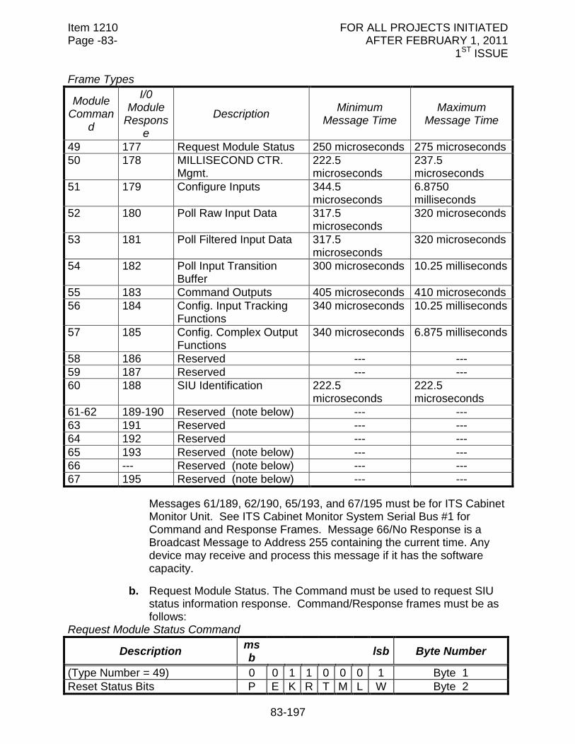
Item 1210 FOR ALL PROJECTS INITIATED Page -83- AFTER FEBRUARY 1, 2011 1ST ISSUE
83-197
Frame Types
Module Comman
d
I/0 Module
Response
Description Minimum
Message Time Maximum
Message Time
49 177 Request Module Status 250 microseconds 275 microseconds
50 178 MILLISECOND CTR. Mgmt.
222.5 microseconds
237.5 microseconds
51 179 Configure Inputs 344.5 microseconds
6.8750 milliseconds
52 180 Poll Raw Input Data 317.5 microseconds
320 microseconds
53 181 Poll Filtered Input Data 317.5 microseconds
320 microseconds
54 182 Poll Input Transition Buffer
300 microseconds 10.25 milliseconds
55 183 Command Outputs 405 microseconds 410 microseconds
56 184 Config. Input Tracking Functions
340 microseconds 10.25 milliseconds
57 185 Config. Complex Output Functions
340 microseconds 6.875 milliseconds
58 186 Reserved --- ---
59 187 Reserved --- ---
60 188 SIU Identification 222.5 microseconds
222.5 microseconds
61-62 189-190 Reserved (note below) --- ---
63 191 Reserved --- ---
64 192 Reserved --- ---
65 193 Reserved (note below) --- ---
66 --- Reserved (note below) --- ---
67 195 Reserved (note below) --- ---
Messages 61/189, 62/190, 65/193, and 67/195 must be for ITS Cabinet Monitor Unit. See ITS Cabinet Monitor System Serial Bus #1 for Command and Response Frames. Message 66/No Response is a Broadcast Message to Address 255 containing the current time. Any device may receive and process this message if it has the software capacity.
b. Request Module Status. The Command must be used to request SIU status information response. Command/Response frames must be as follows:
Request Module Status Command
Description msb
lsb Byte Number
(Type Number = 49) 0 0 1 1 0 0 0 1 Byte 1
Reset Status Bits P E K R T M L W Byte 2
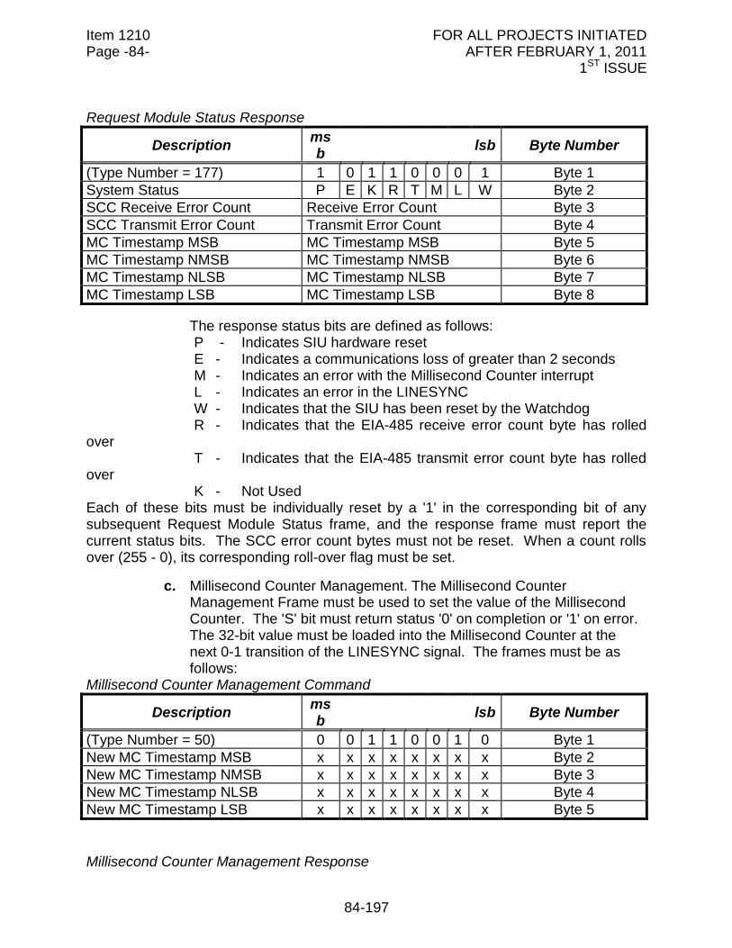
Item 1210 FOR ALL PROJECTS INITIATED Page -84- AFTER FEBRUARY 1, 2011 1ST ISSUE
84-197
Request Module Status Response
Description msb
lsb Byte Number
(Type Number = 177) 1 0 1 1 0 0 0 1 Byte 1
System Status P E K R T M L W Byte 2
SCC Receive Error Count Receive Error Count Byte 3
SCC Transmit Error Count Transmit Error Count Byte 4
MC Timestamp MSB MC Timestamp MSB Byte 5
MC Timestamp NMSB MC Timestamp NMSB Byte 6
MC Timestamp NLSB MC Timestamp NLSB Byte 7
MC Timestamp LSB MC Timestamp LSB Byte 8
The response status bits are defined as follows: P - Indicates SIU hardware reset E - Indicates a communications loss of greater than 2 seconds M - Indicates an error with the Millisecond Counter interrupt L - Indicates an error in the LINESYNC W - Indicates that the SIU has been reset by the Watchdog R - Indicates that the EIA-485 receive error count byte has rolled over T - Indicates that the EIA-485 transmit error count byte has rolled over K - Not Used Each of these bits must be individually reset by a '1' in the corresponding bit of any subsequent Request Module Status frame, and the response frame must report the current status bits. The SCC error count bytes must not be reset. When a count rolls over (255 - 0), its corresponding roll-over flag must be set.
c. Millisecond Counter Management. The Millisecond Counter Management Frame must be used to set the value of the Millisecond Counter. The 'S' bit must return status '0' on completion or '1' on error. The 32-bit value must be loaded into the Millisecond Counter at the next 0-1 transition of the LINESYNC signal. The frames must be as follows:
Millisecond Counter Management Command
Description msb
lsb Byte Number
(Type Number = 50) 0 0 1 1 0 0 1 0 Byte 1
New MC Timestamp MSB x x x x x x x x Byte 2
New MC Timestamp NMSB x x x x x x x x Byte 3
New MC Timestamp NLSB x x x x x x x x Byte 4
New MC Timestamp LSB x x x x x x x x Byte 5
Millisecond Counter Management Response
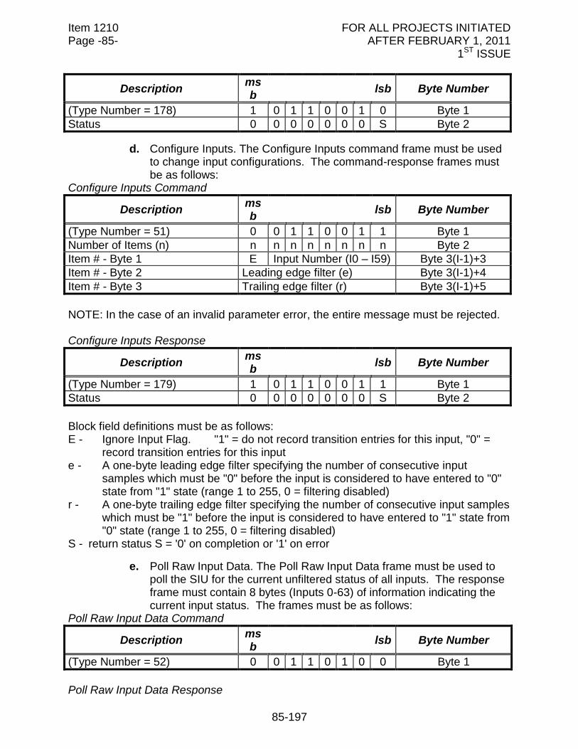
Item 1210 FOR ALL PROJECTS INITIATED Page -85- AFTER FEBRUARY 1, 2011 1ST ISSUE
85-197
Description msb
lsb Byte Number
(Type Number = 178) 1 0 1 1 0 0 1 0 Byte 1
Status 0 0 0 0 0 0 0 S Byte 2
d. Configure Inputs. The Configure Inputs command frame must be used to change input configurations. The command-response frames must be as follows:
Configure Inputs Command
Description msb
lsb Byte Number
(Type Number = 51) 0 0 1 1 0 0 1 1 Byte 1
Number of Items (n) n n n n n n n n Byte 2
Item # - Byte 1 E Input Number (I0 – I59) Byte 3(I-1)+3
Item # - Byte 2 Leading edge filter (e) Byte 3(I-1)+4
Item # - Byte 3 Trailing edge filter (r) Byte 3(I-1)+5
NOTE: In the case of an invalid parameter error, the entire message must be rejected. Configure Inputs Response
Description msb
lsb Byte Number
(Type Number = 179) 1 0 1 1 0 0 1 1 Byte 1
Status 0 0 0 0 0 0 0 S Byte 2
Block field definitions must be as follows: E - Ignore Input Flag. "1" = do not record transition entries for this input, "0" =
record transition entries for this input e - A one-byte leading edge filter specifying the number of consecutive input
samples which must be "0" before the input is considered to have entered to "0" state from "1" state (range 1 to 255, 0 = filtering disabled)
r - A one-byte trailing edge filter specifying the number of consecutive input samples which must be "1" before the input is considered to have entered to "1" state from "0" state (range 1 to 255, 0 = filtering disabled)
S - return status S = '0' on completion or '1' on error
e. Poll Raw Input Data. The Poll Raw Input Data frame must be used to poll the SIU for the current unfiltered status of all inputs. The response frame must contain 8 bytes (Inputs 0-63) of information indicating the current input status. The frames must be as follows:
Poll Raw Input Data Command
Description msb
lsb Byte Number
(Type Number = 52) 0 0 1 1 0 1 0 0 Byte 1
Poll Raw Input Data Response
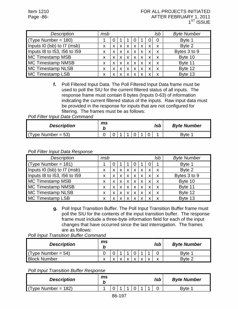
Item 1210 FOR ALL PROJECTS INITIATED Page -86- AFTER FEBRUARY 1, 2011 1ST ISSUE
86-197
Description msb lsb Byte Number
(Type Number = 180) 1 0 1 1 0 1 0 0 Byte 1
Inputs I0 (lsb) to I7 (msb) x x x x x x x x Byte 2
Inputs I8 to I53, I56 to I59 x x x x x x x x Bytes 3 to 9
MC Timestamp MSB x x x x x x x x Byte 10
MC Timestamp NMSB x x x x x x x x Byte 11
MC Timestamp NLSB x x x x x x x x Byte 12
MC Timestamp LSB x x x x x x x x Byte 13
f. Poll Filtered Input Data. The Poll Filtered Input Data frame must be used to poll the SIU for the current filtered status of all inputs. The response frame must contain 8 bytes (Inputs 0-63) of information indicating the current filtered status of the inputs. Raw input data must be provided in the response for inputs that are not configured for filtering. The frames must be as follows:
Poll Filter Input Data Command
Description msb
lsb Byte Number
(Type Number = 53) 0 0 1 1 0 1 0 1 Byte 1
Poll Filter Input Data Response
Description msb lsb Byte Number
(Type Number = 181) 1 0 1 1 0 1 0 1 Byte 1
Inputs I0 (lsb) to I7 (msb) x x x x x x x x Byte 2
Inputs I8 to I53, I56 to I59 x x x x x x x x Bytes 3 to 9
MC Timestamp MSB x x x x x x x x Byte 10
MC Timestamp NMSB x x x x x x x x Byte 11
MC Timestamp NLSB x x x x x x x x Byte 12
MC Timestamp LSB x x x x x x x x Byte 13
g. Poll Input Transition Buffer. The Poll Input Transition Buffer frame must poll the SIU for the contents of the input transition buffer. The response frame must include a three-byte information field for each of the input changes that have occurred since the last interrogation. The frames are as follows:
Poll Input Transition Buffer Command
Description msb
lsb Byte Number
(Type Number = 54) 0 0 1 1 0 1 1 0 Byte 1
Block Number x x x x x x x x Byte 2
Poll Input Transition Buffer Response
Description msb
lsb Byte Number
(Type Number = 182) 1 0 1 1 0 1 1 0 Byte 1
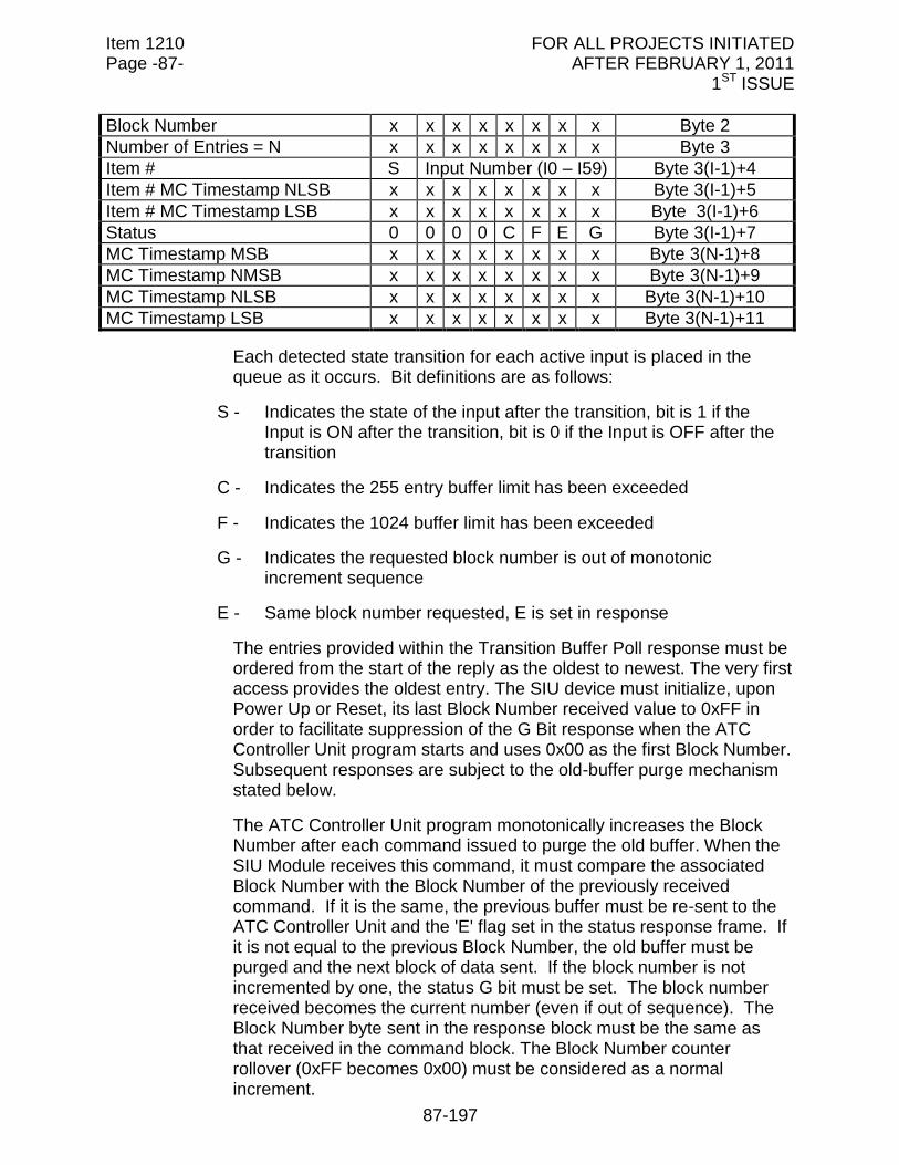
Item 1210 FOR ALL PROJECTS INITIATED Page -87- AFTER FEBRUARY 1, 2011 1ST ISSUE
87-197
Block Number x x x x x x x x Byte 2
Number of Entries = N x x x x x x x x Byte 3
Item # S Input Number (I0 – I59) Byte 3(I-1)+4
Item # MC Timestamp NLSB x x x x x x x x Byte 3(I-1)+5
Item # MC Timestamp LSB x x x x x x x x Byte 3(I-1)+6
Status 0 0 0 0 C F E G Byte 3(I-1)+7
MC Timestamp MSB x x x x x x x x Byte 3(N-1)+8
MC Timestamp NMSB x x x x x x x x Byte 3(N-1)+9
MC Timestamp NLSB x x x x x x x x Byte 3(N-1)+10
MC Timestamp LSB x x x x x x x x Byte 3(N-1)+11
Each detected state transition for each active input is placed in the queue as it occurs. Bit definitions are as follows:
S - Indicates the state of the input after the transition, bit is 1 if the Input is ON after the transition, bit is 0 if the Input is OFF after the transition
C - Indicates the 255 entry buffer limit has been exceeded
F - Indicates the 1024 buffer limit has been exceeded
G - Indicates the requested block number is out of monotonic increment sequence
E - Same block number requested, E is set in response
The entries provided within the Transition Buffer Poll response must be ordered from the start of the reply as the oldest to newest. The very first access provides the oldest entry. The SIU device must initialize, upon Power Up or Reset, its last Block Number received value to 0xFF in order to facilitate suppression of the G Bit response when the ATC Controller Unit program starts and uses 0x00 as the first Block Number. Subsequent responses are subject to the old-buffer purge mechanism stated below.
The ATC Controller Unit program monotonically increases the Block Number after each command issued to purge the old buffer. When the SIU Module receives this command, it must compare the associated Block Number with the Block Number of the previously received command. If it is the same, the previous buffer must be re-sent to the ATC Controller Unit and the 'E' flag set in the status response frame. If it is not equal to the previous Block Number, the old buffer must be purged and the next block of data sent. If the block number is not incremented by one, the status G bit must be set. The block number received becomes the current number (even if out of sequence). The Block Number byte sent in the response block must be the same as that received in the command block. The Block Number counter rollover (0xFF becomes 0x00) must be considered as a normal increment.
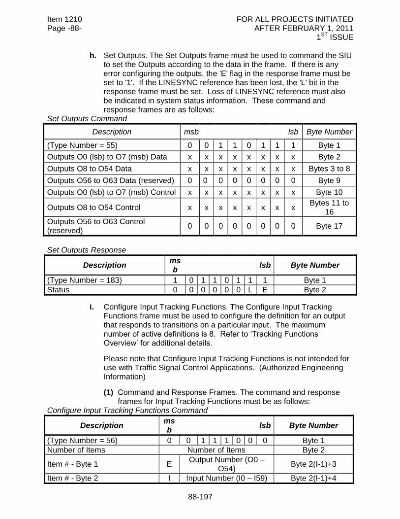
Item 1210 FOR ALL PROJECTS INITIATED Page -88- AFTER FEBRUARY 1, 2011 1ST ISSUE
88-197
h. Set Outputs. The Set Outputs frame must be used to command the SIU to set the Outputs according to the data in the frame. If there is any error configuring the outputs, the 'E' flag in the response frame must be set to '1'. If the LINESYNC reference has been lost, the 'L' bit in the response frame must be set. Loss of LINESYNC reference must also be indicated in system status information. These command and response frames are as follows:
Set Outputs Command
Description msb lsb Byte Number
(Type Number = 55) 0 0 1 1 0 1 1 1 Byte 1
Outputs O0 (lsb) to O7 (msb) Data x x x x x x x x Byte 2
Outputs O8 to O54 Data x x x x x x x x Bytes 3 to 8
Outputs O56 to O63 Data (reserved) 0 0 0 0 0 0 0 0 Byte 9
Outputs O0 (lsb) to O7 (msb) Control x x x x x x x x Byte 10
Outputs O8 to O54 Control x x x x x x x x Bytes 11 to
16
Outputs O56 to O63 Control (reserved)
0 0 0 0 0 0 0 0 Byte 17
Set Outputs Response
Description msb
lsb Byte Number
(Type Number = 183) 1 0 1 1 0 1 1 1 Byte 1
Status 0 0 0 0 0 0 L E Byte 2
i. Configure Input Tracking Functions. The Configure Input Tracking Functions frame must be used to configure the definition for an output that responds to transitions on a particular input. The maximum number of active definitions is 8. Refer to ‘Tracking Functions Overview’ for additional details.
Please note that Configure Input Tracking Functions is not intended for use with Traffic Signal Control Applications. (Authorized Engineering Information)
(1) Command and Response Frames. The command and response frames for Input Tracking Functions must be as follows:
Configure Input Tracking Functions Command
Description msb
lsb Byte Number
(Type Number = 56) 0 0 1 1 1 0 0 0 Byte 1
Number of Items Number of Items Byte 2
Item # - Byte 1 E Output Number (O0 –
O54) Byte 2(I-1)+3
Item # - Byte 2 I Input Number (I0 – I59) Byte 2(I-1)+4
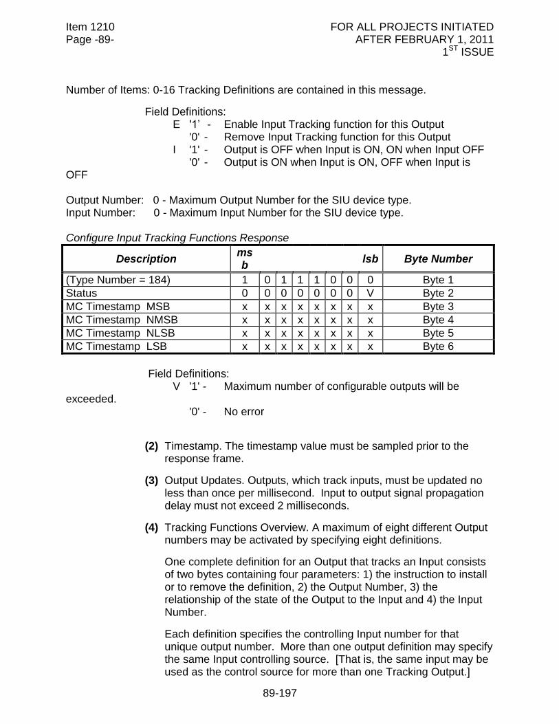
Item 1210 FOR ALL PROJECTS INITIATED Page -89- AFTER FEBRUARY 1, 2011 1ST ISSUE
89-197
Number of Items: 0-16 Tracking Definitions are contained in this message.
Field Definitions: E '1’ - Enable Input Tracking function for this Output '0' - Remove Input Tracking function for this Output I '1' - Output is OFF when Input is ON, ON when Input OFF '0' - Output is ON when Input is ON, OFF when Input is OFF Output Number: 0 - Maximum Output Number for the SIU device type. Input Number: 0 - Maximum Input Number for the SIU device type. Configure Input Tracking Functions Response
Description msb
lsb Byte Number
(Type Number = 184) 1 0 1 1 1 0 0 0 Byte 1
Status 0 0 0 0 0 0 0 V Byte 2
MC Timestamp MSB x x x x x x x x Byte 3
MC Timestamp NMSB x x x x x x x x Byte 4
MC Timestamp NLSB x x x x x x x x Byte 5
MC Timestamp LSB x x x x x x x x Byte 6
Field Definitions: V '1' - Maximum number of configurable outputs will be exceeded. '0' - No error
(2) Timestamp. The timestamp value must be sampled prior to the response frame.
(3) Output Updates. Outputs, which track inputs, must be updated no less than once per millisecond. Input to output signal propagation delay must not exceed 2 milliseconds.
(4) Tracking Functions Overview. A maximum of eight different Output numbers may be activated by specifying eight definitions.
One complete definition for an Output that tracks an Input consists of two bytes containing four parameters: 1) the instruction to install or to remove the definition, 2) the Output Number, 3) the relationship of the state of the Output to the Input and 4) the Input Number.
Each definition specifies the controlling Input number for that unique output number. More than one output definition may specify the same Input controlling source. [That is, the same input may be used as the control source for more than one Tracking Output.]
Item 1210 FOR ALL PROJECTS INITIATED Page -90- AFTER FEBRUARY 1, 2011 1ST ISSUE
90-197
A complete definition is called an Item in the Command Message frame. The ‘Number of Items’ byte specifies the quantity of complete definitions contained in the Command Frame. If the value is 0, all existing active Input Tracking definitions must be removed.
The transmission of a definition may:
(a) install a new active Tracking definition.
(b) remove an existing active Tracking definition. When an Input Tracking definition is removed, the output is set according to the most recently received Set Outputs Command.
(c) convert an active output definition from Complex or Square Wave definition to Tracking. Conversion removes the existing definition and assigns the Tracking definition without a transition through the ‘output is set according to the most recently received Set Outputs Command’ state. The most recent state of the output remains until the new function changes it.
(d) redefine an existing Tracking definition.
If a command frame to be processed by the SIU would result in having more than the maximum number (8) of definitions activated, the entire command frame must be rejected. The response V bit must be set to 1.
The V bit response is based on counting the current active quantity plus the projected Enable definitions after accounting for Remove definitions and invalid Output numbers.
The V bit response evaluation takes the currently active definition quantity, adds the projected Enable definitions, subtracts the Remove definitions, ignores invalid Input and Output numbers and compares the result to the Maximum Number of active Tracking definitions allowed. If the quantity of Active definitions would become greater than the Maximum Number of active Tracking definitions, or if there are more Remove definitions than existing active definitions, the V Bit must be set in the response.
While processing an Enable request, an Out of Range Input number must preclude processing for that definition.
The Out of Range Output and Input numbers must not affect the active definition count. No error response is returned.
The rest of the message must be processed.
The “Number of Items” field is valid from 0 to 16 because the longest message may contain 8 Enable and 8 Remove definitions.
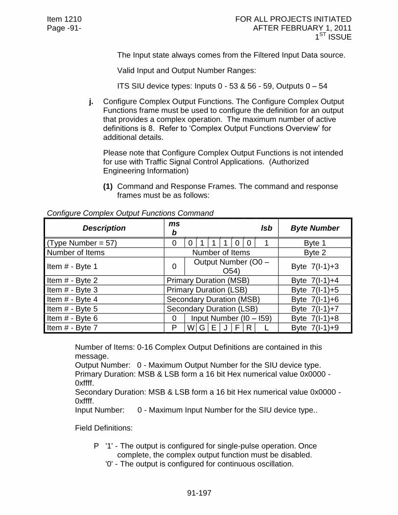
Item 1210 FOR ALL PROJECTS INITIATED Page -91- AFTER FEBRUARY 1, 2011 1ST ISSUE
91-197
The Input state always comes from the Filtered Input Data source.
Valid Input and Output Number Ranges:
ITS SIU device types: Inputs 0 - 53 & 56 - 59, Outputs 0 – 54
j. Configure Complex Output Functions. The Configure Complex Output Functions frame must be used to configure the definition for an output that provides a complex operation. The maximum number of active definitions is 8. Refer to ‘Complex Output Functions Overview’ for additional details.
Please note that Configure Complex Output Functions is not intended for use with Traffic Signal Control Applications. (Authorized Engineering Information)
(1) Command and Response Frames. The command and response frames must be as follows:
Configure Complex Output Functions Command
Description msb
lsb Byte Number
(Type Number = 57) 0 0 1 1 1 0 0 1 Byte 1
Number of Items Number of Items Byte 2
Item # - Byte 1 0 Output Number (O0 –
O54) Byte 7(I-1)+3
Item # - Byte 2 Primary Duration (MSB) Byte 7(I-1)+4
Item # - Byte 3 Primary Duration (LSB) Byte 7(I-1)+5
Item # - Byte 4 Secondary Duration (MSB) Byte 7(I-1)+6
Item # - Byte 5 Secondary Duration (LSB) Byte 7(I-1)+7
Item # - Byte 6 0 Input Number (I0 – I59) Byte 7(I-1)+8
Item # - Byte 7 P W G E J F R L Byte 7(I-1)+9
Number of Items: 0-16 Complex Output Definitions are contained in this message. Output Number: 0 - Maximum Output Number for the SIU device type. Primary Duration: MSB & LSB form a 16 bit Hex numerical value 0x0000 - 0xffff. Secondary Duration: MSB & LSB form a 16 bit Hex numerical value 0x0000 - 0xffff. Input Number: 0 - Maximum Input Number for the SIU device type.. Field Definitions:
P '1' - The output is configured for single-pulse operation. Once complete, the complex output function must be disabled.
'0' - The output is configured for continuous oscillation.
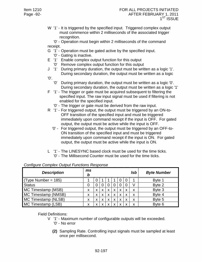
Item 1210 FOR ALL PROJECTS INITIATED Page -92- AFTER FEBRUARY 1, 2011 1ST ISSUE
92-197
W '1' - It is triggered by the specified input. Triggered complex output must commence within 2 milliseconds of the associated trigger recognition.
'0' - Operation must begin within 2 milliseconds of the command receipt.
G '1' - Operation must be gated active by the specified input. '0' - Gating is inactive. E '1' Enable complex output function for this output '0' Remove complex output function for this output J '1' During primary duration, the output must be written as a logic '1'. During secondary duration, the output must be written as a logic
'0'. '0' During primary duration, the output must be written as a logic '0'.
During secondary duration, the output must be written as a logic '1' F '1' - The trigger or gate must be acquired subsequent to filtering the
specified input. The raw input signal must be used if filtering is not enabled for the specified input.
'0' - The trigger or gate must be derived from the raw input. R '1' - For triggered output, the output must be triggered by an ON-to-
OFF transition of the specified input and must be triggered immediately upon command receipt if the input is OFF. For gated output, the output must be active while the input is OFF.
'0' - For triggered output, the output must be triggered by an OFF-to-ON transition of the specified input and must be triggered immediately upon command receipt if the input is ON. For gated output, the output must be active while the input is ON.
L '1' - The LINESYNC based clock must be used for the time ticks.
'0' - The Millisecond Counter must be used for the time ticks.
Configure Complex Output Functions Response
Description msb
lsb Byte Number
(Type Number = 185) 1 0 1 1 1 0 0 1 Byte 1
Status 0 0 0 0 0 0 0 V Byte 2
MC Timestamp (MSB) x x x x x x x x Byte 3
MC Timestamp (NMSB) x x x x x x x x Byte 4
MC Timestamp (NLSB) x x x x x x x x Byte 5
MC Timestamp (LSB) x x x x x x x x Byte 6
Field Definitions: V '1' - Maximum number of configurable outputs will be exceeded.
'0' - No error
(2) Sampling Rate. Controlling input signals must be sampled at least once per millisecond.
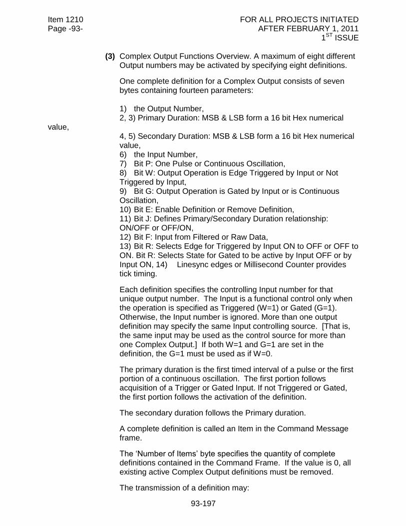
Item 1210 FOR ALL PROJECTS INITIATED Page -93- AFTER FEBRUARY 1, 2011 1ST ISSUE
93-197
(3) Complex Output Functions Overview. A maximum of eight different Output numbers may be activated by specifying eight definitions.
One complete definition for a Complex Output consists of seven bytes containing fourteen parameters:
1) the Output Number, 2, 3) Primary Duration: MSB & LSB form a 16 bit Hex numerical value,
4, 5) Secondary Duration: MSB & LSB form a 16 bit Hex numerical value,
6) the Input Number, 7) Bit P: One Pulse or Continuous Oscillation, 8) Bit W: Output Operation is Edge Triggered by Input or Not
Triggered by Input, 9) Bit G: Output Operation is Gated by Input or is Continuous
Oscillation, 10) Bit E: Enable Definition or Remove Definition, 11) Bit J: Defines Primary/Secondary Duration relationship:
ON/OFF or OFF/ON, 12) Bit F: Input from Filtered or Raw Data, 13) Bit R: Selects Edge for Triggered by Input ON to OFF or OFF to
ON. Bit R: Selects State for Gated to be active by Input OFF or by Input ON, 14) Linesync edges or Millisecond Counter provides tick timing.
Each definition specifies the controlling Input number for that unique output number. The Input is a functional control only when the operation is specified as Triggered (W=1) or Gated (G=1). Otherwise, the Input number is ignored. More than one output definition may specify the same Input controlling source. [That is, the same input may be used as the control source for more than one Complex Output.] If both W=1 and G=1 are set in the definition, the G=1 must be used as if W=0.
The primary duration is the first timed interval of a pulse or the first portion of a continuous oscillation. The first portion follows acquisition of a Trigger or Gated Input. If not Triggered or Gated, the first portion follows the activation of the definition.
The secondary duration follows the Primary duration.
A complete definition is called an Item in the Command Message frame.
The ‘Number of Items’ byte specifies the quantity of complete definitions contained in the Command Frame. If the value is 0, all existing active Complex Output definitions must be removed.
The transmission of a definition may:
Item 1210 FOR ALL PROJECTS INITIATED Page -94- AFTER FEBRUARY 1, 2011 1ST ISSUE
94-197
(a) install a new active Complex Output definition.
(b) remove an existing active Complex Output definition. When a Complex Output definition is removed, the output is set according to the most recently received Set Outputs Command.
(c) convert an active output definition from Tracking or Square Wave definition to Complex Output. Conversion removes the existing definition and assigns the Complex Output definition without a transition through the ‘output is set according to the most recently received Set Outputs Command’ state. The most recent state of the output remains until the new function changes it.
(d) redefine an existing Complex Output definition.
If a command frame to be processed by the SIU would result in having more than the maximum number (8) definitions activated, the entire command frame must be rejected. The response V bit must be set to 1.
The V bit response evaluation takes the currently active definition quantity, adds the projected Enable definitions, subtracts the Remove definitions, ignores invalid Input and Output numbers and compares the result to the maximum number of active Complex definitions allowed. If the quantity of active definitions would become greater than the maximum number of active Complex Output definitions, or if there are more Remove definitions than existing active Complex Output definitions, the V Bit must be set in the response.
While processing an Enable request that requires Triggered or Gated operation, an Out of Range Input number must preclude processing for that definition.
The Out of Range Output and Input numbers must not affect the active definition count. No error response is returned.
The rest of the message must be processed.
The “Number of Items” field is valid from 0 to 16 because the longest message may contain 8 Enable and 8 Remove definitions.
The Input state comes from the Filtered or Raw Input Data source as specified by the Bit F value.
Valid Input and Output Number Ranges: ITS SIU device types: Inputs 0 - 53 & 56 - 59, Outputs 0 – 54
The LINESYNC based clock must used both the rising and falling edges providing a nominal 8.33 millisecond time tick.
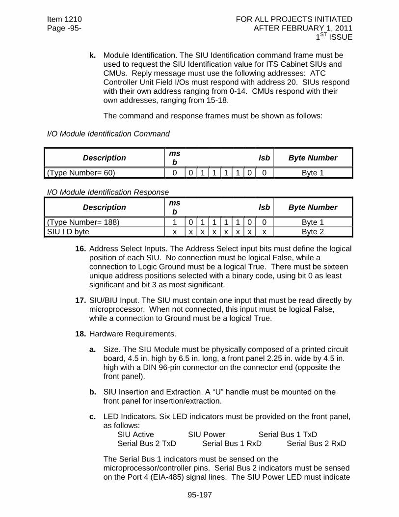
Item 1210 FOR ALL PROJECTS INITIATED Page -95- AFTER FEBRUARY 1, 2011 1ST ISSUE
95-197
k. Module Identification. The SIU Identification command frame must be used to request the SIU Identification value for ITS Cabinet SIUs and CMUs. Reply message must use the following addresses: ATC Controller Unit Field I/Os must respond with address 20. SIUs respond with their own address ranging from 0-14. CMUs respond with their own addresses, ranging from 15-18.
The command and response frames must be shown as follows: I/O Module Identification Command
Description msb
lsb Byte Number
(Type Number= 60) 0 0 1 1 1 1 0 0 Byte 1
I/O Module Identification Response
Description msb
lsb Byte Number
(Type Number= 188) 1 0 1 1 1 1 0 0 Byte 1
SIU I D byte x x x x x x x x Byte 2
16. Address Select Inputs. The Address Select input bits must define the logical position of each SIU. No connection must be logical False, while a connection to Logic Ground must be a logical True. There must be sixteen unique address positions selected with a binary code, using bit 0 as least significant and bit 3 as most significant.
17. SIU/BIU Input. The SIU must contain one input that must be read directly by microprocessor. When not connected, this input must be logical False, while a connection to Ground must be a logical True.
18. Hardware Requirements.
a. Size. The SIU Module must be physically composed of a printed circuit board, 4.5 in. high by 6.5 in. long, a front panel 2.25 in. wide by 4.5 in. high with a DIN 96-pin connector on the connector end (opposite the front panel).
b. SIU Insertion and Extraction. A “U” handle must be mounted on the front panel for insertion/extraction.
c. LED Indicators. Six LED indicators must be provided on the front panel, as follows:
SIU Active SIU Power Serial Bus 1 TxD Serial Bus 2 TxD Serial Bus 1 RxD Serial Bus 2 RxD
The Serial Bus 1 indicators must be sensed on the microprocessor/controller pins. Serial Bus 2 indicators must be sensed on the Port 4 (EIA-485) signal lines. The SIU Power LED must indicate
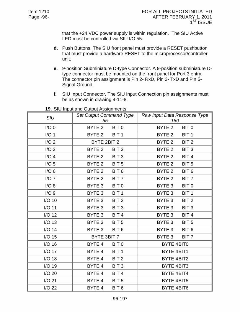
Item 1210 FOR ALL PROJECTS INITIATED Page -96- AFTER FEBRUARY 1, 2011 1ST ISSUE
96-197
that the +24 VDC power supply is within regulation. The SIU Active LED must be controlled via SIU I/O 55.
d. Push Buttons. The SIU front panel must provide a RESET pushbutton that must provide a hardware RESET to the microprocessor/controller unit.
e. 9-position Subminiature D-type Connector. A 9-position subminiature D-type connector must be mounted on the front panel for Port 3 entry. The connector pin assignment is Pin 2- RxD, Pin 3- TxD and Pin 5- Signal Ground.
f. SIU Input Connector. The SIU Input Connection pin assignments must be as shown in drawing 4-11-8.
19. SIU Input and Output Assignments.
SIU Set Output Command Type
55 Raw Input Data Response Type
180
I/O 0 BYTE 2 BIT 0 BYTE 2 BIT 0
I/O 1 BYTE 2 BIT 1 BYTE 2 BIT 1
I/O 2 BYTE 2 BIT 2 BYTE 2 BIT 2
I/O 3 BYTE 2 BIT 3 BYTE 2 BIT 3
I/O 4 BYTE 2 BIT 3 BYTE 2 BIT 4
I/O 5 BYTE 2 BIT 5 BYTE 2 BIT 5
I/O 6 BYTE 2 BIT 6 BYTE 2 BIT 6
I/O 7 BYTE 2 BIT 7 BYTE 2 BIT 7
I/O 8 BYTE 3 BIT 0 BYTE 3 BIT 0
I/O 9 BYTE 3 BIT 1 BYTE 3 BIT 1
I/O 10 BYTE 3 BIT 2 BYTE 3 BIT 2
I/O 11 BYTE 3 BIT 3 BYTE 3 BIT 3
I/O 12 BYTE 3 BIT 4 BYTE 3 BIT 4
I/O 13 BYTE 3 BIT 5 BYTE 3 BIT 5
I/O 14 BYTE 3 BIT 6 BYTE 3 BIT 6
I/O 15 BYTE 3 BIT 7 BYTE 3 BIT 7
I/O 16 BYTE 4 BIT 0 BYTE 4 BIT0
I/O 17 BYTE 4 BIT 1 BYTE 4 BIT1
I/O 18 BYTE 4 BIT 2 BYTE 4 BIT2
I/O 19 BYTE 4 BIT 3 BYTE 4 BIT3
I/O 20 BYTE 4 BIT 4 BYTE 4 BIT4
I/O 21 BYTE 4 BIT 5 BYTE 4 BIT5
I/O 22 BYTE 4 BIT 6 BYTE 4 BIT6
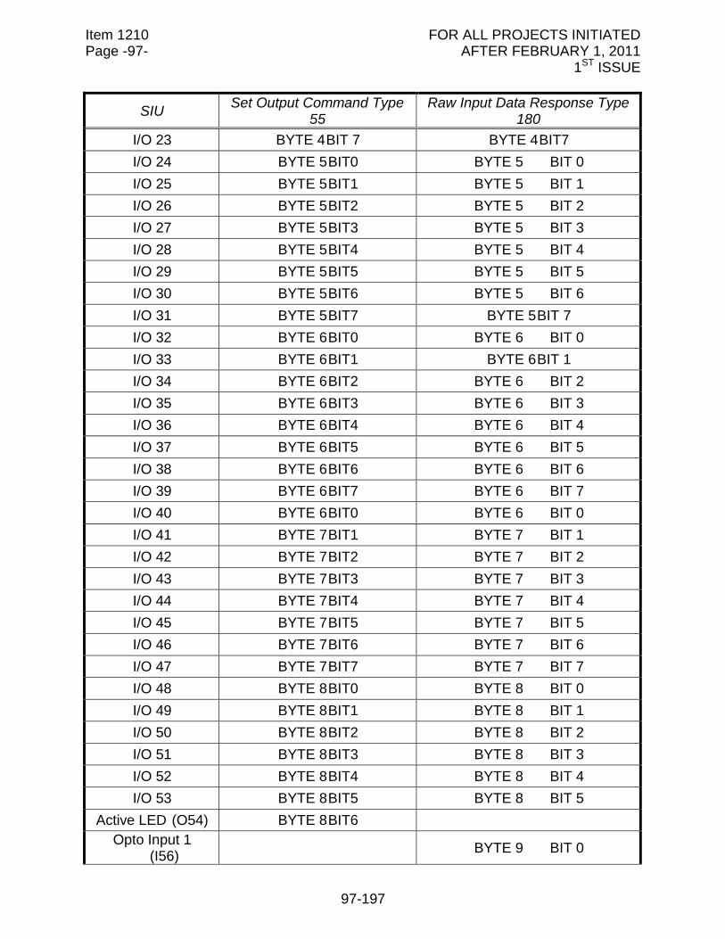
Item 1210 FOR ALL PROJECTS INITIATED Page -97- AFTER FEBRUARY 1, 2011 1ST ISSUE
97-197
SIU Set Output Command Type
55 Raw Input Data Response Type
180
I/O 23 BYTE 4 BIT 7 BYTE 4 BIT7
I/O 24 BYTE 5 BIT0 BYTE 5 BIT 0
I/O 25 BYTE 5 BIT1 BYTE 5 BIT 1
I/O 26 BYTE 5 BIT2 BYTE 5 BIT 2
I/O 27 BYTE 5 BIT3 BYTE 5 BIT 3
I/O 28 BYTE 5 BIT4 BYTE 5 BIT 4
I/O 29 BYTE 5 BIT5 BYTE 5 BIT 5
I/O 30 BYTE 5 BIT6 BYTE 5 BIT 6
I/O 31 BYTE 5 BIT7 BYTE 5 BIT 7
I/O 32 BYTE 6 BIT0 BYTE 6 BIT 0
I/O 33 BYTE 6 BIT1 BYTE 6 BIT 1
I/O 34 BYTE 6 BIT2 BYTE 6 BIT 2
I/O 35 BYTE 6 BIT3 BYTE 6 BIT 3
I/O 36 BYTE 6 BIT4 BYTE 6 BIT 4
I/O 37 BYTE 6 BIT5 BYTE 6 BIT 5
I/O 38 BYTE 6 BIT6 BYTE 6 BIT 6
I/O 39 BYTE 6 BIT7 BYTE 6 BIT 7
I/O 40 BYTE 6 BIT0 BYTE 6 BIT 0
I/O 41 BYTE 7 BIT1 BYTE 7 BIT 1
I/O 42 BYTE 7 BIT2 BYTE 7 BIT 2
I/O 43 BYTE 7 BIT3 BYTE 7 BIT 3
I/O 44 BYTE 7 BIT4 BYTE 7 BIT 4
I/O 45 BYTE 7 BIT5 BYTE 7 BIT 5
I/O 46 BYTE 7 BIT6 BYTE 7 BIT 6
I/O 47 BYTE 7 BIT7 BYTE 7 BIT 7
I/O 48 BYTE 8 BIT0 BYTE 8 BIT 0
I/O 49 BYTE 8 BIT1 BYTE 8 BIT 1
I/O 50 BYTE 8 BIT2 BYTE 8 BIT 2
I/O 51 BYTE 8 BIT3 BYTE 8 BIT 3
I/O 52 BYTE 8 BIT4 BYTE 8 BIT 4
I/O 53 BYTE 8 BIT5 BYTE 8 BIT 5
Active LED (O54) BYTE 8 BIT6
Opto Input 1 (I56)
BYTE 9 BIT 0
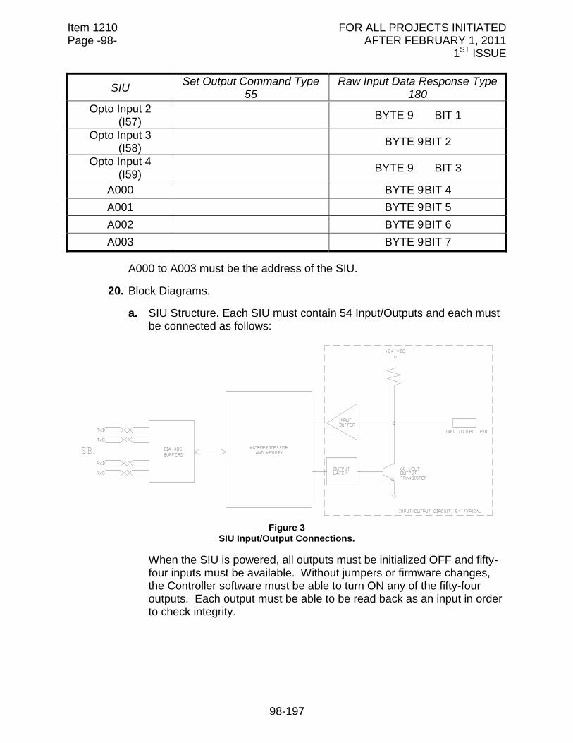
Item 1210 FOR ALL PROJECTS INITIATED Page -98- AFTER FEBRUARY 1, 2011 1ST ISSUE
98-197
SIU Set Output Command Type
55 Raw Input Data Response Type
180
Opto Input 2 (I57)
BYTE 9 BIT 1
Opto Input 3 (I58)
BYTE 9 BIT 2
Opto Input 4 (I59)
BYTE 9 BIT 3
A000 BYTE 9 BIT 4
A001 BYTE 9 BIT 5
A002 BYTE 9 BIT 6
A003 BYTE 9 BIT 7
A000 to A003 must be the address of the SIU.
20. Block Diagrams.
a. SIU Structure. Each SIU must contain 54 Input/Outputs and each must be connected as follows:
Figure 3
SIU Input/Output Connections.
When the SIU is powered, all outputs must be initialized OFF and fifty-four inputs must be available. Without jumpers or firmware changes, the Controller software must be able to turn ON any of the fifty-four outputs. Each output must be able to be read back as an input in order to check integrity.
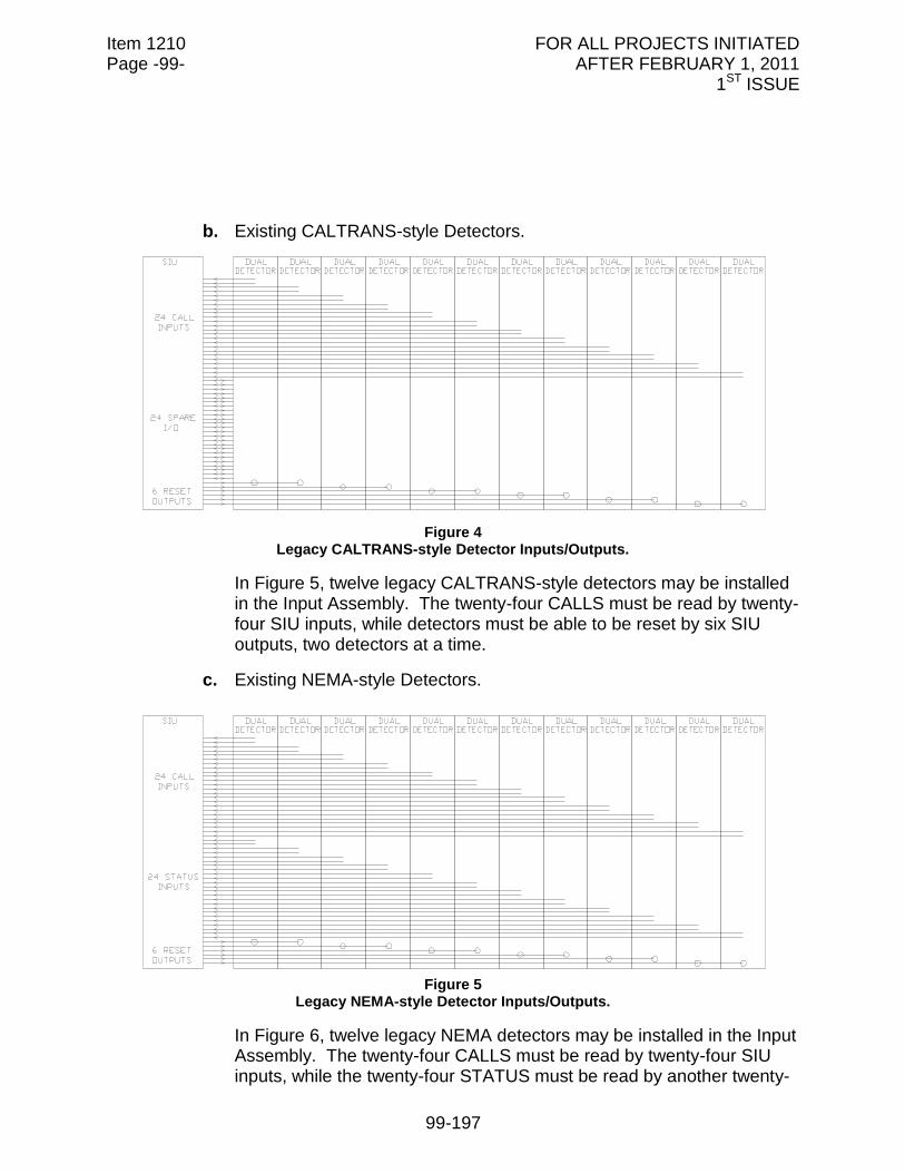
Item 1210 FOR ALL PROJECTS INITIATED Page -99- AFTER FEBRUARY 1, 2011 1ST ISSUE
99-197
b. Existing CALTRANS-style Detectors.
Figure 4
Legacy CALTRANS-style Detector Inputs/Outputs.
In Figure 5, twelve legacy CALTRANS-style detectors may be installed in the Input Assembly. The twenty-four CALLS must be read by twenty-four SIU inputs, while detectors must be able to be reset by six SIU outputs, two detectors at a time.
c. Existing NEMA-style Detectors.
Figure 5
Legacy NEMA-style Detector Inputs/Outputs.
In Figure 6, twelve legacy NEMA detectors may be installed in the Input Assembly. The twenty-four CALLS must be read by twenty-four SIU inputs, while the twenty-four STATUS must be read by another twenty-
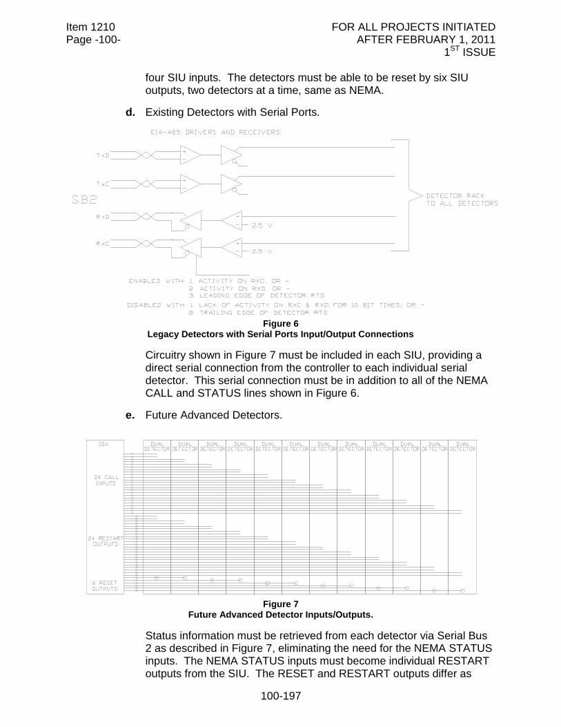
Item 1210 FOR ALL PROJECTS INITIATED Page -100- AFTER FEBRUARY 1, 2011 1ST ISSUE
100-197
four SIU inputs. The detectors must be able to be reset by six SIU outputs, two detectors at a time, same as NEMA.
d. Existing Detectors with Serial Ports.
Figure 6
Legacy Detectors with Serial Ports Input/Output Connections
Circuitry shown in Figure 7 must be included in each SIU, providing a direct serial connection from the controller to each individual serial detector. This serial connection must be in addition to all of the NEMA CALL and STATUS lines shown in Figure 6.
e. Future Advanced Detectors.
Figure 7
Future Advanced Detector Inputs/Outputs.
Status information must be retrieved from each detector via Serial Bus 2 as described in Figure 7, eliminating the need for the NEMA STATUS inputs. The NEMA STATUS inputs must become individual RESTART outputs from the SIU. The RESET and RESTART outputs differ as
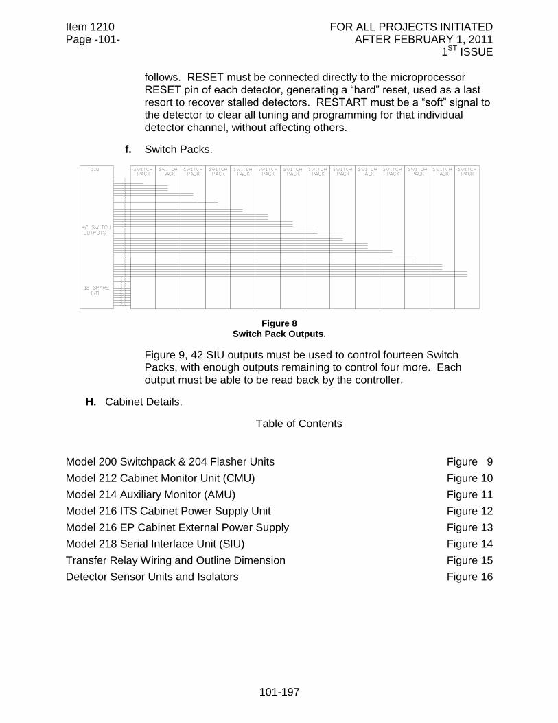
Item 1210 FOR ALL PROJECTS INITIATED Page -101- AFTER FEBRUARY 1, 2011 1ST ISSUE
101-197
follows. RESET must be connected directly to the microprocessor RESET pin of each detector, generating a “hard” reset, used as a last resort to recover stalled detectors. RESTART must be a “soft” signal to the detector to clear all tuning and programming for that individual detector channel, without affecting others.
f. Switch Packs.
Figure 8
Switch Pack Outputs.
Figure 9, 42 SIU outputs must be used to control fourteen Switch Packs, with enough outputs remaining to control four more. Each output must be able to be read back by the controller.
H. Cabinet Details.
Table of Contents
Model 200 Switchpack & 204 Flasher Units Figure 9
Model 212 Cabinet Monitor Unit (CMU) Figure 10
Model 214 Auxiliary Monitor (AMU) Figure 11
Model 216 ITS Cabinet Power Supply Unit Figure 12
Model 216 EP Cabinet External Power Supply Figure 13
Model 218 Serial Interface Unit (SIU) Figure 14
Transfer Relay Wiring and Outline Dimension Figure 15
Detector Sensor Units and Isolators Figure 16
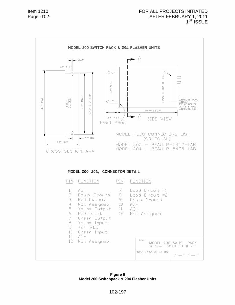
Item 1210 FOR ALL PROJECTS INITIATED Page -102- AFTER FEBRUARY 1, 2011 1ST ISSUE
102-197
Figure 9
Model 200 Switchpack & 204 Flasher Units
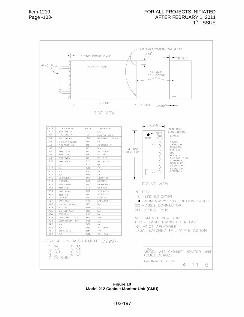
Item 1210 FOR ALL PROJECTS INITIATED Page -103- AFTER FEBRUARY 1, 2011 1ST ISSUE
103-197
Figure 10
Model 212 Cabinet Monitor Unit (CMU)
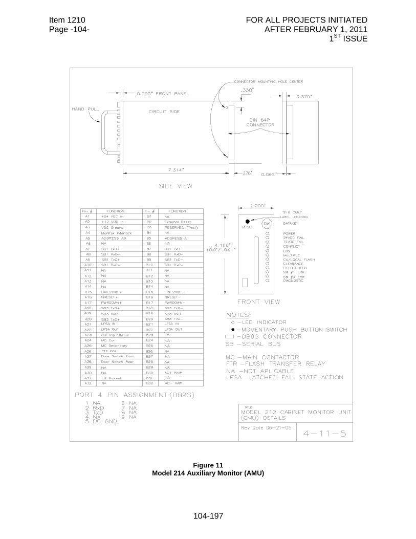
Item 1210 FOR ALL PROJECTS INITIATED Page -104- AFTER FEBRUARY 1, 2011 1ST ISSUE
104-197
Figure 11
Model 214 Auxiliary Monitor (AMU)
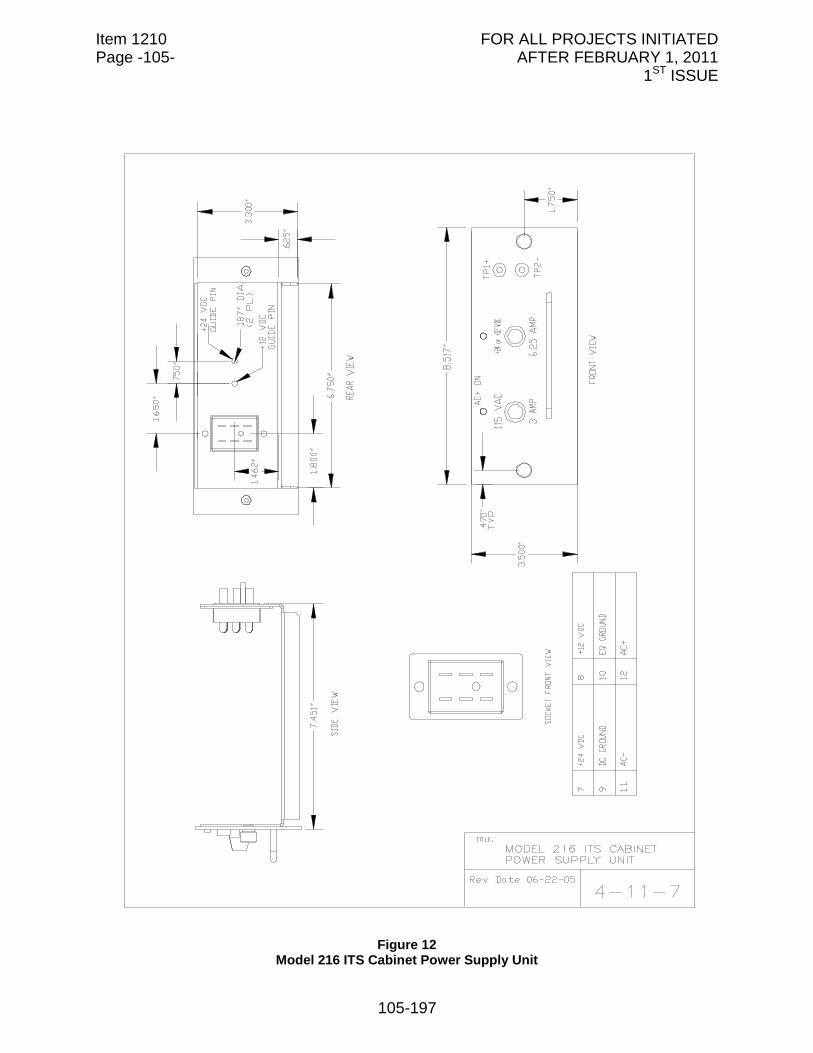
Item 1210 FOR ALL PROJECTS INITIATED Page -105- AFTER FEBRUARY 1, 2011 1ST ISSUE
105-197
Figure 12
Model 216 ITS Cabinet Power Supply Unit
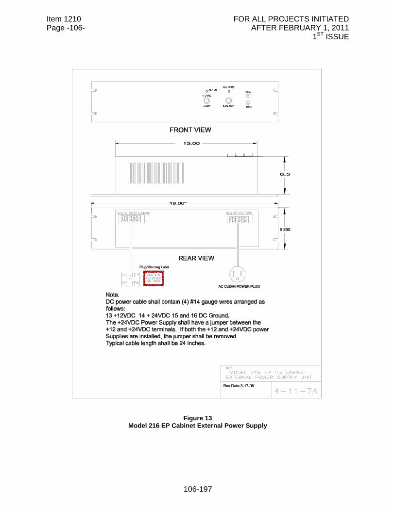
Item 1210 FOR ALL PROJECTS INITIATED Page -106- AFTER FEBRUARY 1, 2011 1ST ISSUE
106-197
Figure 13
Model 216 EP Cabinet External Power Supply
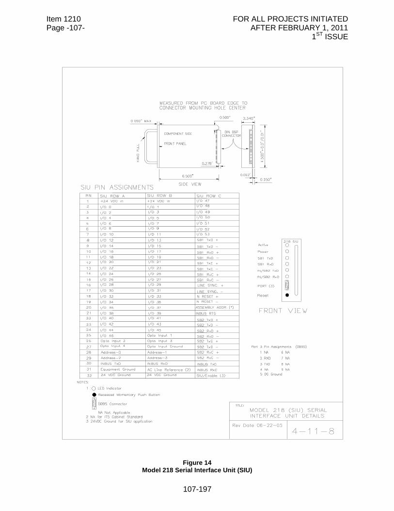
Item 1210 FOR ALL PROJECTS INITIATED Page -107- AFTER FEBRUARY 1, 2011 1ST ISSUE
107-197
Figure 14
Model 218 Serial Interface Unit (SIU)
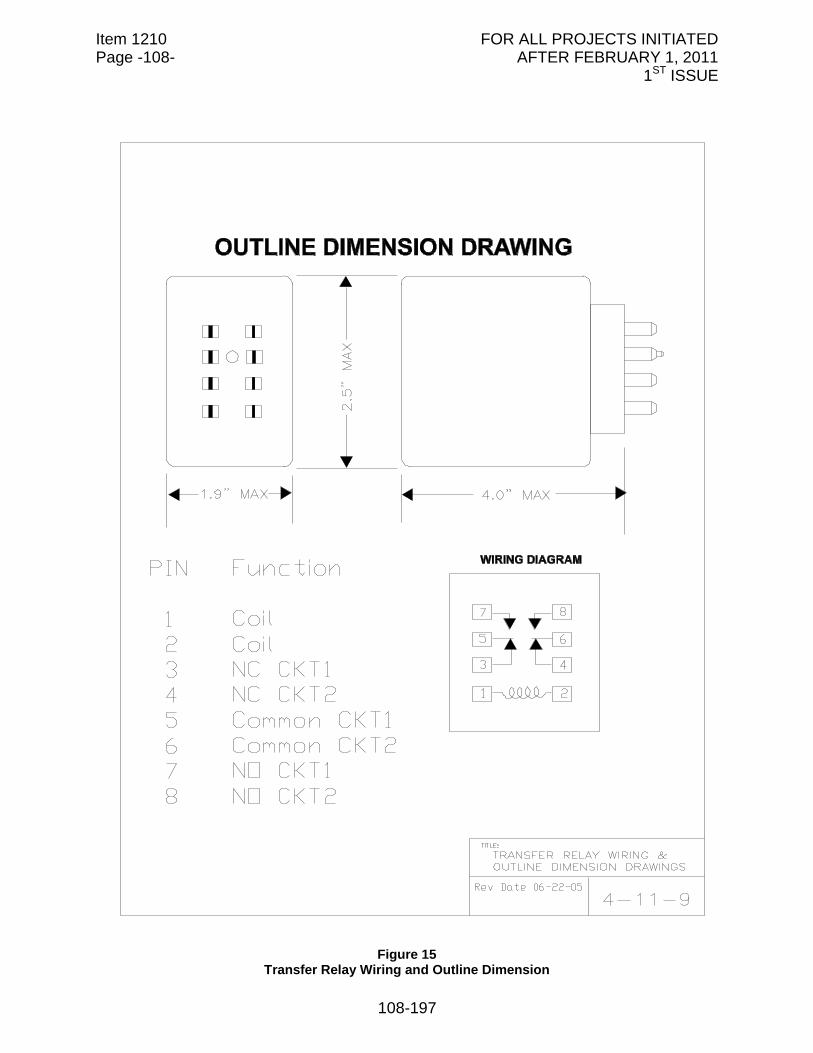
Item 1210 FOR ALL PROJECTS INITIATED Page -108- AFTER FEBRUARY 1, 2011 1ST ISSUE
108-197
Figure 15
Transfer Relay Wiring and Outline Dimension
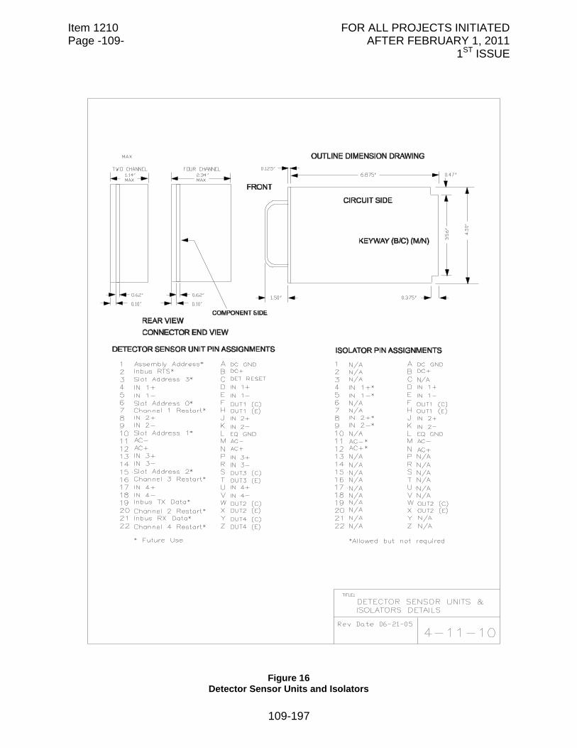
Item 1210 FOR ALL PROJECTS INITIATED Page -109- AFTER FEBRUARY 1, 2011 1ST ISSUE
109-197
Figure 16
Detector Sensor Units and Isolators
Item 1210 FOR ALL PROJECTS INITIATED Page -110- AFTER FEBRUARY 1, 2011 1ST ISSUE
110-197
11. Detector Sensor Units, Elements and Isolators.
A. General Requirements.
1. The sensor and isolator channels must be operationally independent from each other.
2. Each sensor unit or AC isolator channel must draw no more than 100 milliamperes from the +24 VDC cabinet power supply and must be insensitive to 700 millivolts RMS ripple on the incoming +24 VDC line.
3. The sensor unit or isolator front panel must be provided with a hand pull to facilitate insertion and removal from the Input Assembly.
4. All control switches, gain dials and channel indicators must be mounted on the front panel. Each sensor unit or isolator channel must have an indicator to provide visual indication of detector or incoming signal.
5. Each sensor unit or isolator channel output must be an opto-isolated NPN Open Collector capable of sinking 50 milliamperes at 30 VDC. The output must be compatible with the controller unit inputs.
6. A valid channel input must cause a channel Ground True Output to the controller unit of a minimum 100 milliseconds in duration. An onboard physical switching mechanism must be provided to disable this feature when the mechanism is in an OPEN position. Said switching mechanism must eliminate the minimum timing requirement.
7. The output transistor must switch from OFF to ON state or ON to OFF state in 20 microseconds or less.
8. Onboard protection must be provided to enable the sensor unit or isolator to comply with ANSI/IEEE C62.41 (100 Kilohertz Ring Wave and the EFT Burst) at voltages and currents specified at “Location Category A1” (i.e. up to 2.0 Kilovolts, 0.07 Kiloampheres for the 100 Kilohertz Ring Wave) and at “Test Severity” level I (i.e. up to 1.0 Kilovolts, open-circuit) for the EFT Burst.
9. Detector Sensor Units and Isolators must have a front panel mounted test switch for each channel to simulate valid input. The test switch must be a single-pole double-throw, three position CONTROL test switch: The position assignment must be UP = Constant ON; MIDDLE = Normal Operation; and DOWN = Momentary ON.
B. Model 222 & 224 Loop Detector Sensor Unit.
1. General Requirements.
a. The sensor unit channel must produce an output signal when a vehicle passes over or remains over loop wires embedded in the roadway. The method of detection must be based upon a design that renders the output signal when a metallic mass (vehicle) enters the detection zone
Item 1210 FOR ALL PROJECTS INITIATED Page -111- AFTER FEBRUARY 1, 2011 1ST ISSUE
111-197
causing a change of 0.02% minimum decrease in inductance of the circuit measured at the input terminals of the sensor unit.
b. An open loop must cause the sensor unit channel to output a signal indicating a non-detect situation.
c. Each sensor unit channel must be capable of detecting all types of licensed motor vehicles when connected to the loop configuration/lead-in requirements.
d. The sensor unit must comply with all performance requirements when connected to an inductance (loop plus lead-in) from 50 to 700 micro Henries with a Q-parameter as low as 5 at the sensor unit operating frequency.
e. Loop inputs to each channel must be transformer isolated.
f. Each individual channel must have a minimum of 4 switch selectable operating frequencies.
g. The sensor unit channel tuning circuits must be automatic and must be so designed that drift caused by environmental changes or changes in applied power must not cause an actuation.
h. A switch or switch position must be provided on the front panel to disable each channel output.
2. Mode Selection Requirements. Each sensor unit channel must have PULSE and PRESENCE selectable modes.
a. Pulse Mode.
(1) In the PULSE MODE, each new vehicle presence within the detection zone must initiate a sensor unit channel output pulse of 125 milliseconds (+/-25 milliseconds) in duration.
(2) Should a vehicle remain in a portion of the detection zone for a period in excess of 2 seconds, the sensor unit channel must automatically “tune out” the presence of said vehicle. The sensor unit channel must then be capable of detecting another vehicle entering the same detection zone. The recovery time to full sensitivity between the first vehicle pulse and channel capability to detect another vehicle must be 3 seconds maximum.
b. Presence Mode.
(1) In the PRESENCE MODE, the sensor unit channel must recover to normal sensitivity within 1 second after termination of vehicle presence in the detection zone regardless of the duration of the presence.
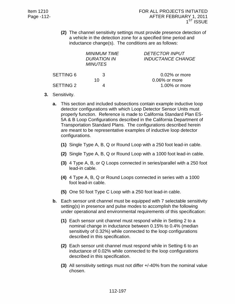
Item 1210 FOR ALL PROJECTS INITIATED Page -112- AFTER FEBRUARY 1, 2011 1ST ISSUE
112-197
(2) The channel sensitivity settings must provide presence detection of a vehicle in the detection zone for a specified time period and inductance change(s). The conditions are as follows:
MINIMUM TIME DETECTOR INPUT DURATION IN INDUCTANCE CHANGE MINUTES
SETTING 6 3 0.02% or more
10 0.06% or more SETTING 2 4 1.00% or more
3. Sensitivity.
a. This section and included subsections contain example inductive loop detector configurations with which Loop Detector Sensor Units must properly function. Reference is made to California Standard Plan ES-5A & B Loop Configurations described in the California Department of Transportation Standard Plans. The configurations described herein are meant to be representative examples of inductive loop detector configurations.
(1) Single Type A, B, Q or Round Loop with a 250 foot lead-in cable.
(2) Single Type A, B, Q or Round Loop with a 1000 foot lead-in cable.
(3) 4 Type A, B, or Q Loops connected in series/parallel with a 250 foot lead-in cable.
(4) 4 Type A, B, Q or Round Loops connected in series with a 1000 foot lead-in cable.
(5) One 50 foot Type C Loop with a 250 foot lead-in cable.
b. Each sensor unit channel must be equipped with 7 selectable sensitivity setting(s) in presence and pulse modes to accomplish the following under operational and environmental requirements of this specification:
(1) Each sensor unit channel must respond while in Setting 2 to a nominal change in inductance between 0.15% to 0.4% (median sensitivity of 0.32%) while connected to the loop configurations described in this specification.
(2) Each sensor unit channel must respond while in Setting 6 to an inductance of 0.02% while connected to the loop configurations described in this specification.
(3) All sensitivity settings must not differ +/-40% from the nominal value chosen.
Item 1210 FOR ALL PROJECTS INITIATED Page -113- AFTER FEBRUARY 1, 2011 1ST ISSUE
113-197
(4) Each sensor unit channel must not detect vehicles, moving or stopped, at distances of 3 feet or more from any loop perimeter, in all configurations listed in this specification.
4. Response Time. Response time of the sensor unit channel for Sensitivity Setting 2 must be less than 5 +/-1 millisecond at an approximate loop frequency of 40 Kilohertz. That is, for any decreased inductive change that exceeds its sensitivity threshold, the channel must output a ground true logic level within 5 millisecond (+/-1 millisecond). When such change is removed, the output must become an open circuit within 5 millisecond (+/-1 millisecond).
5. Beginning of Normal Operation. The sensor unit channels must begin normal operation within 2 seconds after the application of power or after a reset signal of 30 microseconds.
6. Tracking Rate. The sensor unit must be capable of compensating or tracking for an environmental change up to 0.001% change in inductance per second.
7. Tracking Range.
a. The sensor unit must be capable of normal operation as the input inductance is changed from +/-5.0% from the quiescent tuning point regardless of internal circuit drift.
b. The sensor unit must be capable of normal operation as the input resistance is changed from +/-0.5% from the quiescent tuning point regardless of internal circuit drift.
8. Temperature Change. The operation of the sensor unit must not be affected by changes in the inductance and/or capacitance of the loop caused by environmental changes, with the rate of temperature change not exceeding 1 degree C per 3 minutes. The opening or closing of the controller cabinet door with a temperature differential of up to 18 degrees C between the inside and outside air must not affect the proper operation of the sensor unit.
C. Magnetic Detector Requirements.
1. The Model 232 Two-Channel Magnetic Detector Sensor Unit must provide 2 channels of detection. When resident in an energized cabinet Input Assembly, and each channel connected to its associated Model 231 Magnetic Detector Sensing Element(s), the channel must produce a continuous output signal to the controller unit when a voltage is induced in the sensing element by a vehicle passing over the sensing element.
2. Each channel must detect vehicles passing within 6 feet of the Model 231 Sensing Element with 1000 feet of lead-in cable, at all speeds between 3 and 80 miles per hour.
Item 1210 FOR ALL PROJECTS INITIATED Page -114- AFTER FEBRUARY 1, 2011 1ST ISSUE
114-197
3. A single control knob for adjusting the sensitivity of each channel must be mounted on the front panel and must be readily adjustable without the use of tools.
4. A momentary switch or switch position must be provided to place a call on each channel, on an individual basis.
D. Model 242 Two-Channel DC Isolator.
1. General Requirements.
a. The Model 242 Two-Channel DC Isolator must contain 2 isolation channels which provide isolation between electrical contacts external to the module and the controller unit input. The method of isolation must be based upon a design which must provide reliable operation.
b. The isolator must have an internal power supply supplying 20 VDC (+/-4 VDC) to the field input side of the isolation channels. The isolator must not draw more than 2.5 Watts of AC power. No current must be drawn from the cabinet power supply.
c. A channel contact closure input of 5 milliseconds or less must not cause an output (ground true) to the controller. An input of 25 milliseconds or greater must cause an output to the controller. An input of duration between 5 and 25 milliseconds may or may not cause an output to the controller. The channel circuitry must be able to react to a new input closure within 25 milliseconds of an input opening.
d. Each isolation channel field input must be turned ON (TRUE) when a contact closure causes an input voltage of less than 8 VDC, and must be turned OFF (FALSE) when the contact opening causes the input voltage to exceed 12 VDC. Each input must deliver no less than 15 milliamperes, nor more than 40 milliamperes, to an electrical contact closure or short from the power supply.
E. Model 252 Two-Channel AC Isolator.
1. General Requirements.
a. The Model 252 Two-Channel AC Isolator must contain 2 isolation channels which provide isolation between external 120 VAC input circuits and the controller unit input circuits. The method of isolation must be based upon a design that provides reliable operation.
b. A channel input voltage “Von” of 80 VAC (+/-5 VAC) applied for a minimum duration of 120 milliseconds (+/-10 milliseconds) must cause an output (Ground True) to the controller unit.
c. A channel input voltage “Voff” (Von minus 10 VAC) applied for a minimum duration of 120 milliseconds (+/-10 milliseconds) must cause an output (Ground False) to the controller unit.
Item 1210 FOR ALL PROJECTS INITIATED Page -115- AFTER FEBRUARY 1, 2011 1ST ISSUE
115-197
d. A two-post jumper must be provided to select inverted output states for Von and Voff. When in CLOSED position (Grounded), Von must cause a Ground False output. An indicator must be provided on the front panel labeled ‘RR” which must indicate a Voff input, Ground True output.
e. The input impedance of each channel must be between 6,000 - 15,000 Ohms at 60 Hertz.
f. The minimum isolation must be 1000 Megohms between the input and output terminals at 500 AC applied voltage.
12. Cabinet System Requirements.
A. General.
1. The Intelligent Transportation System (ITS) Serial Interconnected Cabinet Family is a group of cabinets designed to fulfill a variety of applications. This chapter describes the functional and physical requirements of said cabinets.
2. There are common parts to all cabinets, such as Modular Bus and Power Assemblies, ATC Controller Unit, Power Distribution Assembly (PDA ITS), and Input and Output Assemblies. The Housing and the Cage(s) must depend on the housing configuration.
3. The ATC Controller Unit is serially connected to the Cabinet via two serial synchronous ports located at the Field I/O C12 Connector or the CPU-1B C13 Connector (Serial Bus 1 only). These two communication links use EIA-485 Drivers/Receivers and Synchronous Data Link Control (SDLC) Protocol to interface with Serial Bus #1 and #2.
B. Cabinet Model Number and Consistency.
1. The ITS Cabinets must consist of a package of items needed to carry out a specific Application. Cabinet Versions provided here are EXAMPLES of possible cabinet configurations. A Product Implementation Conformance Statement is provided as an Annex to this standard:
Cabinet Traffic Signal Application - Series 340 340 - 4 Door Cabinet with “P” Base Ground Mount 342 - 2 Door Cabinet with “170” Base Ground Mount 346 - 2 Door Cabinet with ”170” Base, Adaptor Mount
Cabinet Traffic Management Application - Series 350 354 - 2 Door Cabinet with “170” Base Ground Mount 356 - 2 Door Cabinet with “170” Base Adaptor Mount
Table 2
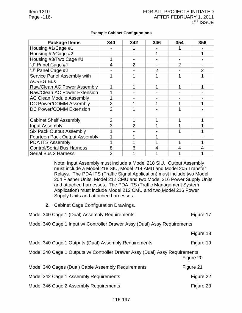
Item 1210 FOR ALL PROJECTS INITIATED Page -116- AFTER FEBRUARY 1, 2011 1ST ISSUE
116-197
Example Cabinet Configurations
Package Items 340 342 346 354 356 Housing #1/Cage #1 - 1 - 1 - Housing #2/Cage #2 - - 1 - 1 Housing #3/Two Cage #1 1 - - - - “J” Panel Cage #1 4 2 - 2 -
“J” Panel Cage #2 - - 2 - 2 Service Panel Assembly with AC-/EG Bus
1 1 1 1 1
Raw/Clean AC Power Assembly 1 1 1 1 1 Raw/Clean AC Power Extension 1 - - - - AC Clean Module Assembly 1 - - - -
DC Power/COMM Assembly 2 1 1 1 1 DC Power/COMM Extension
2 1 - 1 -
Cabinet Shelf Assembly 2 1 1 1 1 Input Assembly 3 2 1 1 1 Six Pack Output Assembly 1 - - 1 1 Fourteen Pack Output Assembly 1 1 1 - - PDA ITS Assembly 1 1 1 1 1 Control/Serial Bus Harness 8 6 4 4 4 Serial Bus 3 Harness 3 1 1 1 1
Note: Input Assembly must include a Model 218 SIU. Output Assembly must include a Model 218 SIU, Model 214 AMU and Model 205 Transfer Relays. The PDA ITS (Traffic Signal Application) must include two Model 204 Flasher Units, Model 212 CMU and two Model 216 Power Supply Units and attached harnesses. The PDA ITS (Traffic Management System Application) must include Model 212 CMU and two Model 216 Power Supply Units and attached harnesses.
2. Cabinet Cage Configuration Drawings.
Model 340 Cage 1 (Dual) Assembly Requirements Figure 17
Model 340 Cage 1 Input w/ Controller Drawer Assy (Dual) Assy Requirements
Figure 18
Model 340 Cage 1 Outputs (Dual) Assembly Requirements Figure 19
Model 340 Cage 1 Outputs w/ Controller Drawer Assy (Dual) Assy Requirements Figure 20
Model 340 Cages (Dual) Cable Assembly Requirements Figure 21
Model 342 Cage 1 Assembly Requirements Figure 22
Model 346 Cage 2 Assembly Requirements Figure 23
Item 1210 FOR ALL PROJECTS INITIATED Page -117- AFTER FEBRUARY 1, 2011 1ST ISSUE
117-197
Model 354 Cage 1 Assembly Requirements Figure 24
Model 356 Cage 2 Assembly Requirements Figure 25
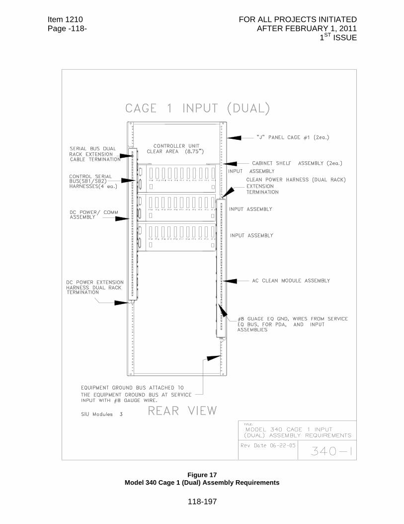
Item 1210 FOR ALL PROJECTS INITIATED Page -118- AFTER FEBRUARY 1, 2011 1ST ISSUE
118-197
Figure 17
Model 340 Cage 1 (Dual) Assembly Requirements
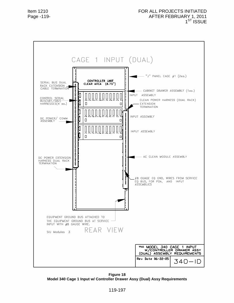
Item 1210 FOR ALL PROJECTS INITIATED Page -119- AFTER FEBRUARY 1, 2011 1ST ISSUE
119-197
Figure 18
Model 340 Cage 1 Input w/ Controller Drawer Assy (Dual) Assy Requirements
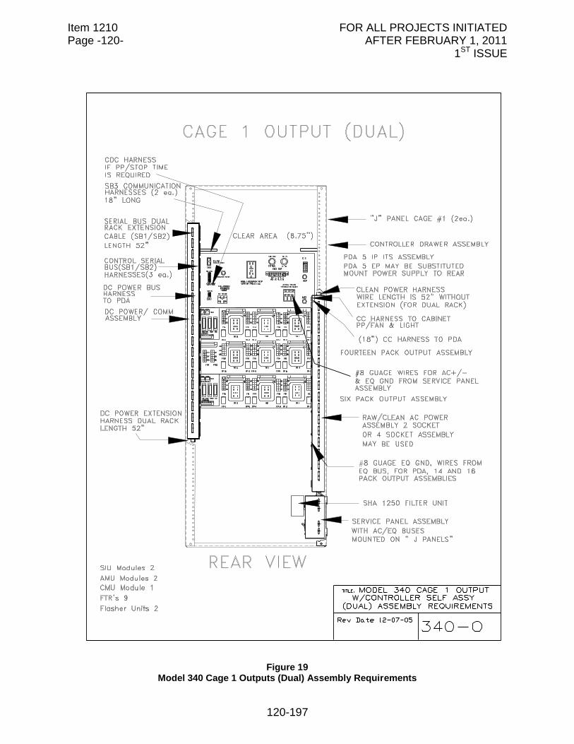
Item 1210 FOR ALL PROJECTS INITIATED Page -120- AFTER FEBRUARY 1, 2011 1ST ISSUE
120-197
Figure 19
Model 340 Cage 1 Outputs (Dual) Assembly Requirements
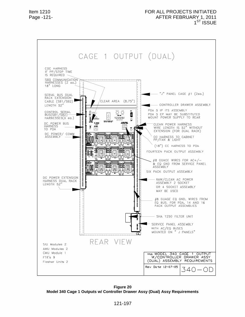
Item 1210 FOR ALL PROJECTS INITIATED Page -121- AFTER FEBRUARY 1, 2011 1ST ISSUE
121-197
Figure 20
Model 340 Cage 1 Outputs w/ Controller Drawer Assy (Dual) Assy Requirements
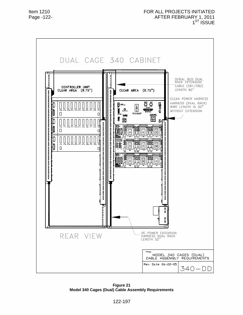
Item 1210 FOR ALL PROJECTS INITIATED Page -122- AFTER FEBRUARY 1, 2011 1ST ISSUE
122-197
Figure 21
Model 340 Cages (Dual) Cable Assembly Requirements
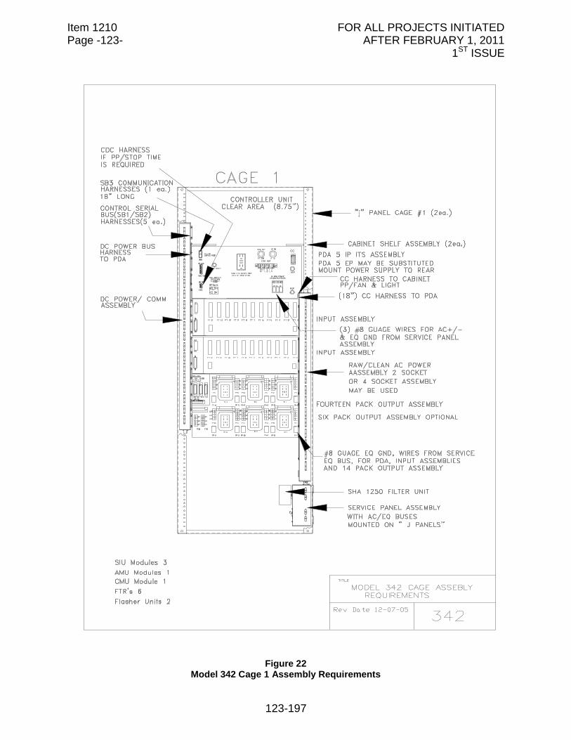
Item 1210 FOR ALL PROJECTS INITIATED Page -123- AFTER FEBRUARY 1, 2011 1ST ISSUE
123-197
Figure 22
Model 342 Cage 1 Assembly Requirements
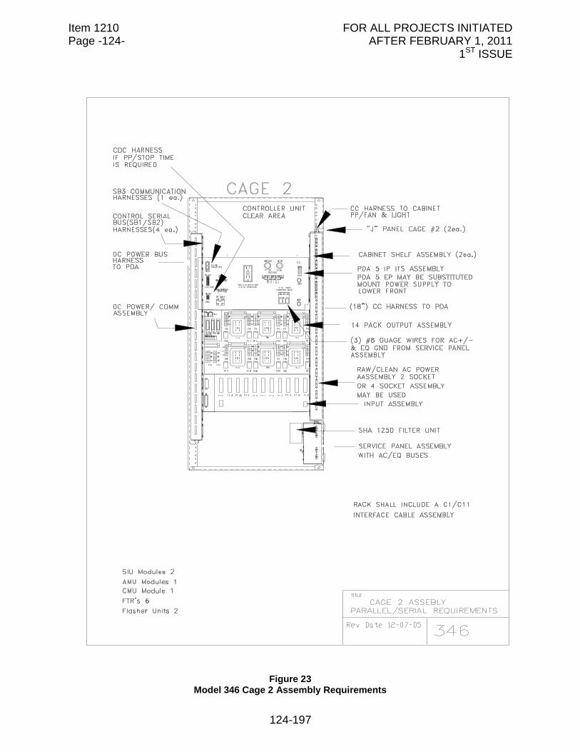
Item 1210 FOR ALL PROJECTS INITIATED Page -124- AFTER FEBRUARY 1, 2011 1ST ISSUE
124-197
Figure 23
Model 346 Cage 2 Assembly Requirements
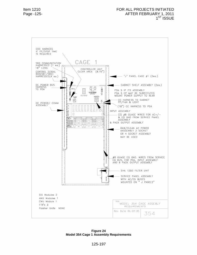
Item 1210 FOR ALL PROJECTS INITIATED Page -125- AFTER FEBRUARY 1, 2011 1ST ISSUE
125-197
Figure 24
Model 354 Cage 1 Assembly Requirements
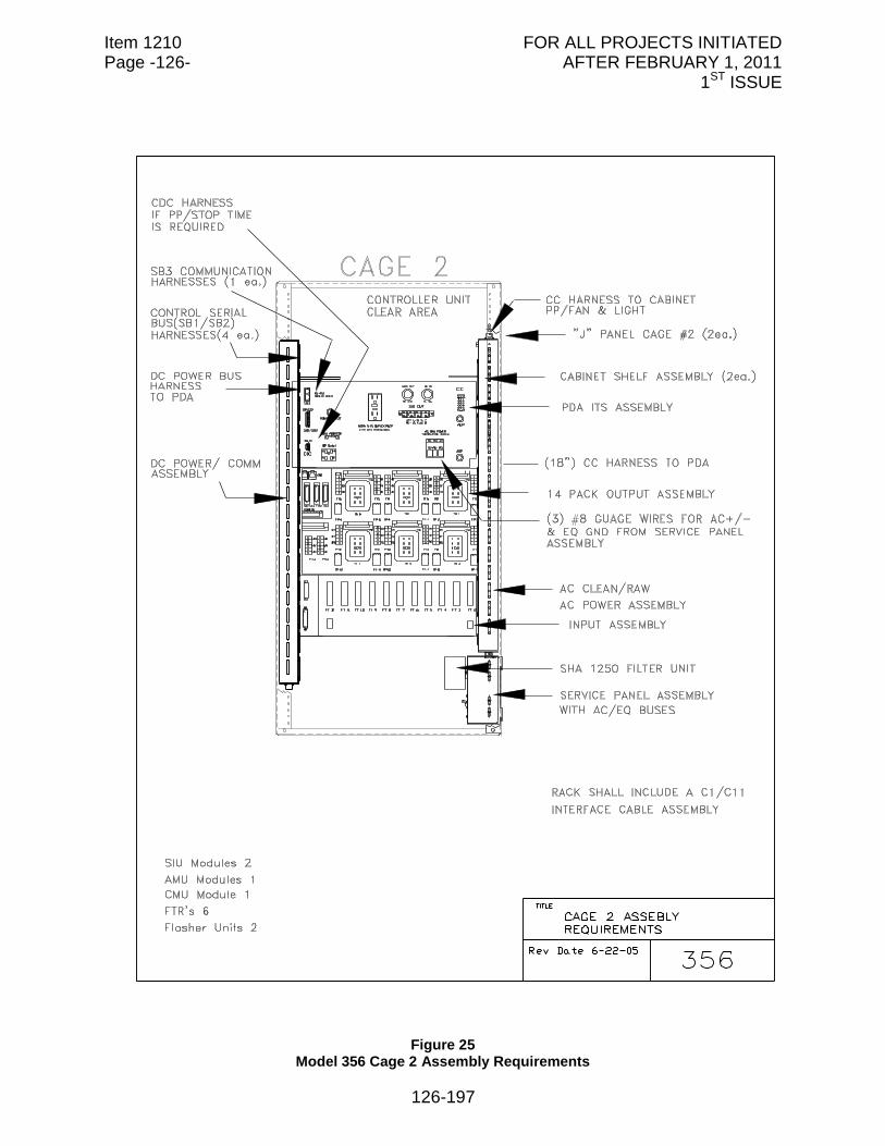
Item 1210 FOR ALL PROJECTS INITIATED Page -126- AFTER FEBRUARY 1, 2011 1ST ISSUE
126-197
Figure 25
Model 356 Cage 2 Assembly Requirements
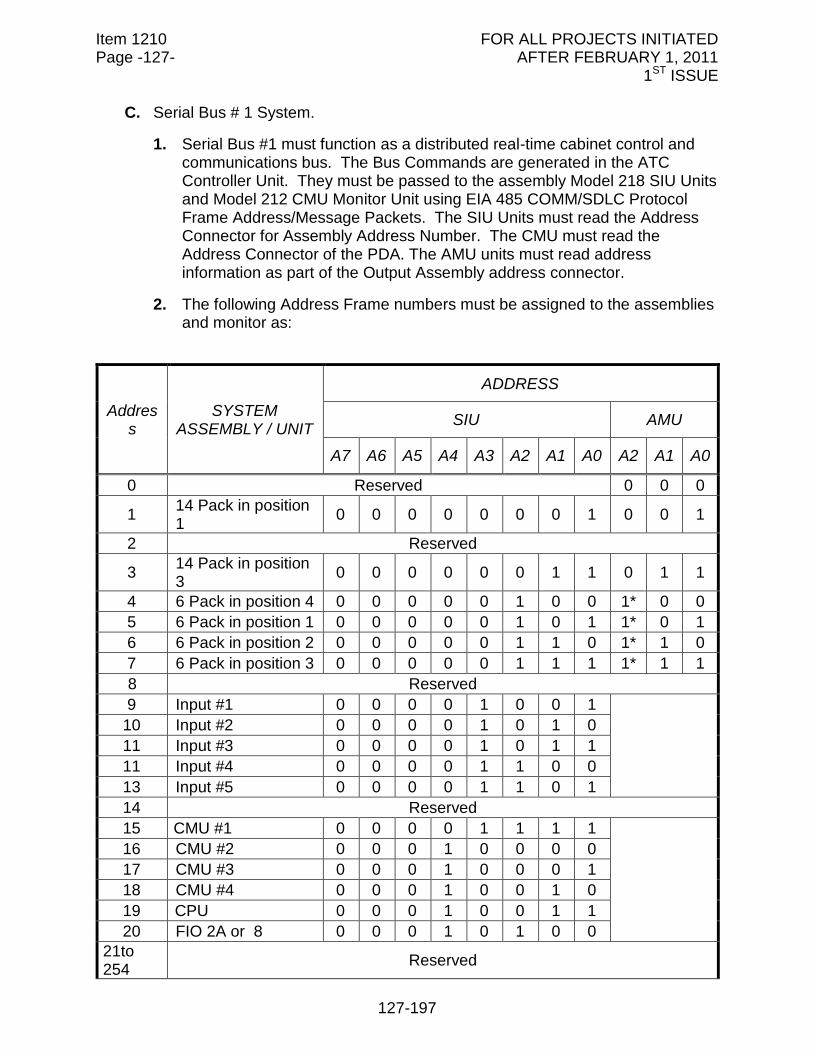
Item 1210 FOR ALL PROJECTS INITIATED Page -127- AFTER FEBRUARY 1, 2011 1ST ISSUE
127-197
C. Serial Bus # 1 System.
1. Serial Bus #1 must function as a distributed real-time cabinet control and communications bus. The Bus Commands are generated in the ATC Controller Unit. They must be passed to the assembly Model 218 SIU Units and Model 212 CMU Monitor Unit using EIA 485 COMM/SDLC Protocol Frame Address/Message Packets. The SIU Units must read the Address Connector for Assembly Address Number. The CMU must read the Address Connector of the PDA. The AMU units must read address information as part of the Output Assembly address connector.
2. The following Address Frame numbers must be assigned to the assemblies and monitor as:
Address
SYSTEM ASSEMBLY / UNIT
ADDRESS
SIU AMU
A7 A6 A5 A4 A3 A2 A1 A0 A2 A1 A0
0 Reserved 0 0 0
1 14 Pack in position 1
0 0 0 0 0 0 0 1 0 0 1
2 Reserved
3 14 Pack in position 3
0 0 0 0 0 0 1 1 0 1 1
4 6 Pack in position 4 0 0 0 0 0 1 0 0 1* 0 0
5 6 Pack in position 1 0 0 0 0 0 1 0 1 1* 0 1
6 6 Pack in position 2 0 0 0 0 0 1 1 0 1* 1 0
7 6 Pack in position 3 0 0 0 0 0 1 1 1 1* 1 1
8 Reserved
9 Input #1 0 0 0 0 1 0 0 1
10 Input #2 0 0 0 0 1 0 1 0
11 Input #3 0 0 0 0 1 0 1 1
11 Input #4 0 0 0 0 1 1 0 0
13 Input #5 0 0 0 0 1 1 0 1
14 Reserved
15 CMU #1 0 0 0 0 1 1 1 1
16 CMU #2 0 0 0 1 0 0 0 0
17 CMU #3 0 0 0 1 0 0 0 1
18 CMU #4 0 0 0 1 0 0 1 0
19 CPU 0 0 0 1 0 0 1 1
20 FIO 2A or 8 0 0 0 1 0 1 0 0
21to 254
Reserved
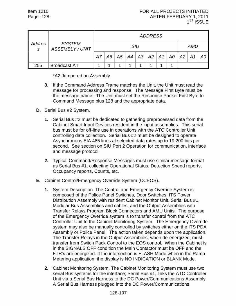
Item 1210 FOR ALL PROJECTS INITIATED Page -128- AFTER FEBRUARY 1, 2011 1ST ISSUE
128-197
Address
SYSTEM ASSEMBLY / UNIT
ADDRESS
SIU AMU
A7 A6 A5 A4 A3 A2 A1 A0 A2 A1 A0
255 Broadcast All 1 1 1 1 1 1 1 1
*A2 Jumpered on Assembly
3. If the Command Address Frame matches the Unit, the Unit must read the message for processing and response. The Message First Byte must be the message name. The Unit must set the Response Packet First Byte to Command Message plus 128 and the appropriate data.
D. Serial Bus #2 System.
1. Serial Bus #2 must be dedicated to gathering preprocessed data from the Cabinet Smart Input Devices resident in the input assemblies. This serial bus must be for off-line use in operations with the ATC Controller Unit controlling data collection. Serial Bus #2 must be designed to operate Asynchronous EIA 485 lines at selected data rates up to 19,200 bits per second. See section on SIU Port 2 Operation for communication, interface and message protocol.
2. Typical Command/Response Messages must use similar message format as Serial Bus #1, collecting Operational Status, Detection Speed reports, Occupancy reports, Counts, etc.
E. Cabinet Control/Emergency Override System (CCEOS).
1. System Description. The Control and Emergency Override System is composed of the Police Panel Switches, Door Switches, ITS Power Distribution Assembly with resident Cabinet Monitor Unit, Serial Bus #1, Modular Bus Assemblies and cables, and the Output Assemblies with Transfer Relays Program Block Connectors and AMU Units. The purpose of the Emergency Override system is to transfer control from the ATC Controller Unit to the Cabinet Monitoring System. The Emergency Override system may also be manually controlled by switches either on the ITS PDA Assembly or Police Panel. The action taken depends upon the application. The Transfer Relays in the Output Assemblies, when de-energized, must transfer from Switch Pack Control to the EOS control. When the Cabinet is in the SIGNALS OFF condition the Main Contactor must be OFF and the FTR’s are energized. If the intersection is FLASH Mode when in the Ramp Metering application, the display is NO INDICATION or BLANK Mode.
2. Cabinet Monitoring System. The Cabinet Monitoring System must use two serial Bus systems for the interface; Serial Bus #1, links the ATC Controller Unit via a Serial Bus Harness to the DC Power/Communications Assembly. A Serial Bus Harness plugged into the DC Power/Communications
Item 1210 FOR ALL PROJECTS INITIATED Page -129- AFTER FEBRUARY 1, 2011 1ST ISSUE
129-197
Assembly must connect to the 212 Cabinet Monitor Unit with application serial memory key resident in the PDA ITS.
Serial Bus #3 Harnesses must provide the interconnection between the Output Assembly’s 214 Auxiliary Monitor Units and the CMU. The Bus Harnesses must be daisy chained between the Output Assemblies and the PDA ITS. See sections CMU and AMU sections for operations, functions, protocol, Message frames and bit rate.
F. Housings.
1. Housing Package. The housings must include, but not be limited to, the following:
a. Enclosure & Doors
b. Gasketing
c. Lifting Eyes & External Bolt Heads
d. Door Latches & Locks
e. Ventilation
f. Cage Supports & Mounting
g. Door Hinges & Catches
h. Police Panel
i. Aluminum Surfaces
2. Housing Construction. The housing must be rainproof. It must have front and rear doors, each equipped with a lock and handle. The enclosure top must be crowned to prevent standing water. The aluminum surface must be either coated with a Mill Finish or Anti-Graffiti Paint.
a. Material Thickness. The enclosure, doors, lifting eyes, gasket channels, police panel door, spacer supports and all supports welded to the enclosure and doors must be fabricated of 0.125 in. minimum thickness aluminum sheet. The filter shell, filter trough, fan support and police panel enclosure must be fabricated of 0.080 in. minimum thickness aluminum sheet. The spacer supports must have the option to use 0.059 in. minimum stainless steel sheet.
b. Welds. All exterior seams for enclosure and doors must be continuously welded and must be smooth. All edges must be filled to a radius of 0.03125 in. minimum. Exterior cabinet welds must be done by gas Tungsten arc TIG process only. ER5356 aluminum alloy bare welding electrodes conforming to AWS A5.10 requirements must be used for welding on aluminum. Procedures, welders and welding operators must conform to the requirements and practices in AWS B3.0 and C5.6
Item 1210 FOR ALL PROJECTS INITIATED Page -130- AFTER FEBRUARY 1, 2011 1ST ISSUE
130-197
for aluminum. Internal cabinet welds must be done by gas metal arc MIG or gas Tungsten arc TIG Process.
c. Aluminum Surface Protection. ALUMINUM SURFACE PROTECTION must be either MILL FINISH or ANTI-GRAFFITI Paint.
(1) Anti – Graffiti Paint. The aluminum surface must be cleaned, etched and rinsed. The cleaning and etching procedure must be to immerse in inhabited alkaline cleaner at 71 degrees C for five minutes (Oakite 61A, Diversey 909 or equivalent in mix of the 6 to 8 ounces per gallon to distilled water). Rinse in cold water. Etch in a sodium solution at 66 degrees C for 5 minutes 90.5 ounce sodium fluoride plus 5 ounces of sodium hydroxide mix per gallon to distilled water. Rinse in cold water. Desmut in a 50% by volume nitric acid solution at 20 degrees C for 2 minutes. Rinse in cold water. Dry surfaces by preheating in an oven for 15 minutes at 400 degrees F. Remove and coat the surfaces using TCI Wheel Silver # 9811- 0110 with a minimum film build of not more than 2 mils total thickness. Place back into preheated oven for 10 minutes minimum at 360 degrees F to gel the base coat. Remove and coat the surfaces using TCI Anti-graffiti Clear # 9810-0231. Place back into oven and fully cure at 380 degrees F for 40 minutes.
d. Enclosure Door Frames and Door Seals. The enclosure door frames must be double flanged out on all four sides and must have strikers to hold tension on, and form a firm seal between, the door gasketing and the frame. The dimension between the door edge and the enclosure external surface when the door is closed and locked must be 0.156 in. (+/-0.08 in.).
3. Gasketing. Gasketing must be provided on all door openings and must be dust-tight. Gaskets must be 0.25 in. minimum thickness closed cell neoprene or silicone (BOYD R- 108480 or equal) and must be permanently bonded to the metal. A gasket top and side channels must be provided to support the top gasket on the door to prevent gasket gravitational fatigue.
4. Cage Mounting Supports. Cage mounting supports must be provided on either side, level with the bottom edge of the door opening, for horizontal support and bolt attachment; side cage supports provided for the bracket cage supports; and bracket cage support attachments.
5. Lifting Eyes and Exterior Bolt Heads. The housing must be provided with 2 lifting eyes for placing the cabinet on its foundation. Each eye opening must have a minimum diameter of 0.75 in.. Each eye must be able to support the weight load of 1000 lbs. All bolt heads must be tamperproof type.
6. Door Latches and Locks. The latching handles must have provision for padlocking in the closed position. Each handle must be 0.75 in. minimum diameter stainless steel with a minimum of 0.50 in. shank. The padlocking
Item 1210 FOR ALL PROJECTS INITIATED Page -131- AFTER FEBRUARY 1, 2011 1ST ISSUE
131-197
attachment must be placed at 4 in. from the handle shank center. An additional 4 in. minimum gripping length must be provided.
a. Latch/Lock Mechanism. The latching mechanism must be a three-point draw roller type. The pushrods must be turned edgewise at the outward supports and have a cross section of 0.25 in. thick by 0.75 in. wide minimum. Rollers must have a minimum diameter of 0.875 in. with nylon wheels and steel ball bearings. When the door is closed and latched, the door must be locked. The lock and lock support must be rigidly mounted on the door. The lock must be mounted in the upper quadrant, above the handle when in it’s full open position. In the locked position, the bolt throw must extend a minimum of 0.25 in. (+/-0.03125 in.) into the latch cam area. A seal must be provided to prevent dust or water entry through the lock opening.
b. Lock and Keys. The locks must be Corbin 2 type. One key must be supplied with each lock. The keys must be removable in the locked position only. The locks must have rectangular, spacing loaded bolts. The bolt must have a 0.281 in. throw and must be 0.75 in. wide by 0.375 in. thick. Tolerance is 0.035 in.. A swing away cover must be placed over the key entrance to protect the lock mechanism.
c. Cam. The center latch cam must be fabricated of a minimum thickness of 0.188 in. aluminum, or 11 gauge steel. The bolt surface must horizontally cover the cam thickness. The cam must be structured to only allow the door to open when the handle is moved toward the center of the door.
7. Housing Ventilation. Housing Ventilation must including intake, exhaust, filtration, and continuous running fan assembly, or a thermostat controlled fan.
a. Intake & Filter. The louvered vent depth must be a maximum of 0.25 in.. A removable and reusable air filter must be housed behind the door vents. The filter filtration area must cover the vent opening area. A filter shell must be provided that fits over the filter providing mechanical support for the filter. This shell must be louvered to direct the incoming air downward. The shell sides and top must be bent over a minimum of 0.25 in. to house the filter. The filter resident in its shell must be held firmly in place with a bottom trough and spring loaded upper clamp. No incoming air must bypass the filter. The bottom filter trough must be formed into a waterproof sump with drain holes to the outside housing. The filter must be 16 in. wide by 12 in. high by 0.875 in. thick. The filter must be an ECO-AIR Product E35S or equal. The intake (including filter with shell) and exhaust areas must pass a minimum of 60 cubic feet of air per minute for Housing #1; 120 cubic feet of air per minute for Housing #3; and 26 cubic feet of air per minute for Housing #2.
b. Fan. Each electric fan must be equipped with ball or roller bearings and must have a minimum capacity of 100 cubic feet of free air delivery per

Item 1210 FOR ALL PROJECTS INITIATED Page -132- AFTER FEBRUARY 1, 2011 1ST ISSUE
132-197
minute. The fan must be mounted within the housing and protected with a finger guard.
8. Hinges. Stainless Steel hinges (Two-bolts per leaf) must be provided to bolt the enclosure to the doors. Housing #1 & Housing #3 must have four hinges per door and Housing #2 must have three hinges per door. Each hinge must be 3-1/2 in. minimum length and have a fixed pin. The pin ends must be welded to hinge and ground smooth. The pins and bolts must be covered by the door edge and not accessible when the door is closed. A ground strap between the door and the main cabinet housing must be required when 120 VAC components are mounted on the door.
9. Door Catches. Front and rear doors must be provided with catches to hold the door open at both 90 and 165 (+/-10 degrees). The catch minimum diameter must be 0.375 in. aluminum rods. The catches must be capable of holding the door open at 90 degrees in a 60 mph wind acting at an angle perpendicular to the plane of the door.
10. Police Panel. A police panel assembly must be provided to allow the limited control access. The panel door must be equipped with a lock and master police key. The front and back of the panel must be enclosed with a rigid metal covering so that no parts having live voltage are exposed. The panel assembly must have a drain to prevent water from collecting within the assembly. The drain must be channeled to the outside. The series 35X Cabinets must have one switch provided and labeled "SIGNALS ON - OFF ". The series 34X Cabinets must have one switch labeled "SIGNALS ON - OFF" and the other "FLASH/AUTO". The MANUAL CONTROL ENABLE ON-OFF switch and a receptacle for the INTERVAL ADVANCE cord must be provided. A 12 VAC transformer must be provided in advance of the INTERVAL ADVANCE receptacle. An INTERVAL ADVANCE cord, six feet in length, must be provided.
G. Rack Cage. A Standard Rack Cage must be installed inside the housing for mounting of the ATC Controller Unit and cabinet assemblies. The EIA rack portion of the cage must consist of four continuous, adjustable equipment mounting angles. The mounting angle nominal thickness must be 11 gauge plated steel. The mounting angles must be tapped with 10-32 threads with EIA universal spacing. The mounting angle must comply with standard EIA-310-B and must be supported at the top and bottom by either welded or bolted support angles to form a cage. The mounting angles must provide holes to mount the “J” panels.
1. Clearance Between Rails. Clearance between rails for mounting assemblies must be 17.75 in..
2. Cage Connection. The cage must be bolted to the cabinet at 4 points via the housing cage supports and 4 points via associated spacer brackets (top and bottom).
Item 1210 FOR ALL PROJECTS INITIATED Page -133- AFTER FEBRUARY 1, 2011 1ST ISSUE
133-197
3. Cage Location. The cage(s) must be centered within the cabinet door opening(s).
H. Cabinet Assemblies.
1. General.
a. Cabinet Assemblies. The cabinet assemblies must be completely removable from or installable in the cabinet cage without removing any other equipment and using only a Standard Slotted or Phillips Screwdriver.
b. Visible and Accessible Devices. All fuses, circuit breakers, switches (except Police Panel Switches and Fan Fuse) and indicators must be readily visible and accessible when the cabinet front door is open.
c. Labels and Marker Strips. All equipment in the cabinet must be clearly and permanently labeled. The marker strips must be made of material that can be easily and legibly written on using a pencil or ballpoint pen. Marker strips must be located immediately below the item they are to identify and must be clearly visible with the items installed.
d. Resistor/Capacitor Suppression. Suppression must be provided at all relay sockets (across relay coil), except for the Transfer Relays (TR) in the output assemblies where one suppression device may be common for all.
e. PDA, Output and Input Assemblies. PDA, Output and Input Assemblies Depth must include terminal sockets, plug-in units and strain relief bar (Field Wire Support Bracket). The Width must be 17.5 in. maximum including side screws. The maximum Depth, including connectors, must not exceed 14.0 in. The assembly housing top and bottom must be slotted for vertical ventilation. Assembly Thickness - Side ends must be fabricated of 0.080 in. minimum thickness aluminum sheet. All other surfaces must be fabricated of 0.0625 in. minimum thickness aluminum sheet. The aluminum metal surface must be treated with clear chromate.
f. Connector Sockets. Flasher and Switch Pack Unit sockets must be mounted with their front face 7.50 in. from the assembly front panel.
g. Nylon Guides. Guides (top and bottom) must be provided for assembly Plug-in units (Power Supply Units guide on bottom only). The guides must begin 0.50 in. from the assembly front panel face.
2. “J” Panel Assemblies. The “J” Panels must be mirror images of each other when mounted in the cabinet cage. They must be bolted to the cage with the matching shelf unit bolted to the panel. Two ten position minimum AC- Raw & Equipment Ground Copper Bus Bars must be provided on the lower right position of the J Panel when viewed from the rear door for interconnect
Item 1210 FOR ALL PROJECTS INITIATED Page -134- AFTER FEBRUARY 1, 2011 1ST ISSUE
134-197
to the Service Panel and provide the termination of AC- Raw and Equipment Ground wiring within the Cage and Cabinet.
a. Input Termination Panel Assembly. An optional Input Termination Panel must be provided that uses ten twelve-position terminal blocks and 4 copper bus bars. Eight of the twelve position terminal blocks and the four copper bus bars must be used for termination of field inputs. Two of the twelve position terminal blocks must be used for termination of the CDC interface. Input transient protection devices may be used for input termination. Terminal blocks one through four provide termination for Input Assembly #1 and terminal blocks five through eight provide termination for Input Assembly #2. A ground lug must be provided on the panel assembly to terminate an 8 AWG green wire that is attached to the Equipment Ground copper bus bar on the “J” panel assembly. The Input Termination Panel must be mounted on the left side of the Rack Assembly, when viewing from the rear.
3. Cabinet Shelf Assemblies. A Shelf Assembly must be provided unless otherwise called out in the contract special provisions. One alternative is a shelf/drawer assembly.
4. Service Panel Assembly.
a. General Requirements. A Service Panel Assembly must be provided. The assembly must function as the entry point for AC Power to the cabinet including main and secondary circuit breakers, cabinet transient and voltage surge protection, clean power filtering, Raw and Clean AC Power Source.
b. Location. The assembly must be located on the lower right J Panel when viewed from the back door.
c. Service Terminal Block. The terminals of the Block must be labeled AC+, AC- and EG and must be covered with a clear insulating material to prevent inadvertent contact. The Terminating Lugs must be large enough to accommodate # 2 conductors.
d. AC+ Raw, AC- Raw and Equipment Ground Bus Termination. This assembly must provide two 8 in. #8 gauge wire extensions for AC- Raw and Equipment Ground, for attachment to the AC- and Ground busses mounted on the “J” panel.
e. The DC Ground and Equipment Ground Bus must be electrically isolated by 500 Megohms when tested at 250 VDC.
f. The AC- copper terminal bus must not be grounded to the cabinet or connected to logic ground. Nylon screws with a minimum diameter of 0.25 in. or nylon spacers must be used for securing the bus to the J Panel.
Item 1210 FOR ALL PROJECTS INITIATED Page -135- AFTER FEBRUARY 1, 2011 1ST ISSUE
135-197
5. Raw/Clean AC Power Assembly. This Assembly must be provided in each cabinet. It must provide Six Clean AC Power Receptacles for assemblies and cabinet units; Raw AC Power to the Output Assemblies; and both logic and power to the Fan and Light system, door opening circuitry and logic interface (all via CCIN and CCOUT Connectors).
a. Raw/Clean AC Power Extension. The Extension must provide a minimum of five additional NEMA 5-15 receptacles with harness plug connector for plugging into the main assembly. The extension may be an option in Housing #1, and must be required in Cage 2 of the Housing #3.
6. DC Power/Communications Assembly. This assembly must function as the DC Power bus, providing Six VDC BEAU S5404-SB Receptacles and communications interface between the ATC Controller Unit and other assemblies. This assembly must interface with ATC Controller Unit Logic Lines (Power Down, NRESET and LINESYNC) and Seven System Serial Bus signals via DB-25S Connectors.
a. DC Power/Communications Extension. The Extension must provide additional Serial Bus Connectors and DC Receptacles. The extension may be an option.
b. Terminator Unit. A Serial Bus #1 and #2 Terminator Unit must be provided and plugged into the DC POWER / COMMUNICATIONS ASSEMBLY DB 25S End Connector. The Terminator Unit must provide a 150 ohm termination resistor between the RxD+ and RxD-, the TxD+ and TxD-, the RxC+ and RxC-, and the TxC+ and TxC- pairs for both Serial Bus #1 and Serial Bus #2.
The Terminator Unit must also provide 1K ohm DC bias resistors from +5VDC ISO to the RxD+, the RxC+, the TxD+, and the TxC+ of both Serial Bus #1 and Serial Bus #2. The Terminator Unit must provide 1K ohm DC bias resistors from ISO GND to the RxD-, the RxC-, the TxD-, and the TxC- of both Serial Bus #1 and Serial Bus #2.
7. Power Distribution Assembly ITS.
a. The Power Distribution Assembly ITS is an EIA-310B rack mounted assembly that provides for the protection and distribution of AC power and DC power. Additionally:
(1) Logic control circuits, including a Main Contactor for control of the load circuits;
(2) Fault sensing field Circuit Breakers, eight for Traffic applications and four for Traffic Management systems.
(3) Production and distribution of DC power, using +12VDC and 24VDC pluggable power supplies.
Item 1210 FOR ALL PROJECTS INITIATED Page -136- AFTER FEBRUARY 1, 2011 1ST ISSUE
136-197
(4) A resident Cabinet Monitor Unit (CMU).
(5) Maintenance service, consisting of a circuit breaker in line with GFI equipment power receptacles.
(6) Two Model 204 Flasher Units, protected by a ganged two pole 20 A Circuit Breaker when operating in a Traffic Signal application.
(7) A 25 Pin D Socket must be provided for communication with the ATC Controller Unit. This Socket must be mated with an 18in. Communications Cable. This Cable must be attached to the Assembly by slotted 4:40 screws. See Serial Bus Harnesses Detail 6-5-39.
(8) A four position Address Socket and plug must be provided to provide addressing to the CMU.
b. A CDC Connector must be provided on the rear panel of the Output Assembly for isolated signal outputs from the police panel. The CDC Socket is a 9 Pin “D” connector that contains the Manual Control Enable, Stop Time, Interval Advance, and Manual Flash switch signals. The Manual Control Enable and Manual Flash switch signals must be a 120 VAC signal in series with a 27K Ohm resistor. The Interval Advance and Stop Time switch signals must be 12 VAC signals from a transformer located in the PDA. The secondary output of the 12 VAC transformer must be tied to AC- RAW. CDC pin 5 Common must be referenced to AC- RAW. CDC pins 8 must provide an interface for the external reset signal and 9 must provide an interface for DC Ground.
c. The PDA must be provided with eight field load circuit breakers and two Model 204 Flasher Units with ganged circuit beaker protection. The Load Circuit Breakers located on the PDA that are used to control the Output Assembly Model 200 Switch Pack Units must have auxiliary switches. The auxiliary switches must “open” when the load breaker has tripped and the system will transfer the power from the Main Contactor to the Flash or Blank condition.
d. The Amperage Rating of breakers must be shown on the face of the breaker or handle. Breaker function must be labeled below the breakers on the front panel. Ganged Circuit Breakers must be assembled by the circuit breaker manufacturer and certified that their circuit breakers must gang trip.
e. The maintenance equipment circuit must include a 15-Ampere Circuit Breaker in line with GFCI receptacles on both the front and back of the assembly. The back receptacle must be the first with GFCI Protection device as defined in the National Electrical Code. Circuit interruption must occur on 6 milliamperes of ground fault-current and must not occur less than 4 milliamperes of ground-fault current. The front receptacle must be attached to the load side of the GFCI device.
Item 1210 FOR ALL PROJECTS INITIATED Page -137- AFTER FEBRUARY 1, 2011 1ST ISSUE
137-197
f. The AUTO/FLASH Switch when placed in FLASH position must de-energize the Main Contactor and the Transfer Relays (TR) Coils. When the switch is placed in the AUTO position must energize the Main Contactor and the TR Coils. The switch must be a SPST Control Switch.
g. The DC Power must be brought to the back panel using a BEAU S5404-SB Receptacle. An 18 in. DC Power (DCP) Harness, with sheath, consisting of 4 #18 cables, with a BEAU P5404-LAB Connector on each end, must be provided with the Assembly. The harness must be plugged in to an adjacent plug on the DC/COMM Assembly. See detail 6-5-40 of this specification.
h. Three 36 in. minimum length #8 gauge wires, one black for AC+, one white for AC- and one green or green/yellow for Equipment Ground, must be attached to the rear of the assembly at the AC Raw Power Terminating Block. The cables must be routed between the Service Panel Assembly AC+ terminal, the AC-Bus and the Equipment Ground Bus.
The PDA Assembly must have a resident 18 in. ACP Harness with sheath and strain relief. The other end must contain a BEAU P5412-CCE connector. This harness must be plugged into the P1 connector on the Raw/Clean AC Power Assembly. The ACP harness must provide Flasher input and AC power to the Switch Packs.
An 18 in. long CC Harness must be provided with sheath and strain relief. When plugged into the Raw/Clean AC Power Assembly (CC IN) this harness must provide AC Raw voltage and control logic between the ITS PDA Assembly and the Police Panel control switches.
An 18 in. long ACCP power cord with strain relief and a NEMA 5-15 plug must provide AC Clean power to the PDA ITS Assembly when plugged into the Raw/Clean Power Assembly.
i. A capacitive load of 1 microFarad at 400 VAC must be provided across each Flasher Unit Output.
8. Input Assembly.
a. The Input Assembly must be an EIA-310B rack mounted assembly providing twelve slots of 22/44 pin PCB sockets. A Model 218 Serial Interface Unit (SIU) must be provided in its location mated to a DIN 96-Pin Connector. The SIU must provide interface and control between the ATC Controller Unit and the input units via System Serial Bus #1 and #2. See Section Model 218 SIU for System Operation and Interface. A 25 Pin D Socket must be provided for communication with the ATC Controller Unit. This Socket must be mated with an 18 in. Communications Cable. This Cable must be attached to the Assembly by slotted 4:40 screws. See Serial Bus Harnesses Detail.
Item 1210 FOR ALL PROJECTS INITIATED Page -138- AFTER FEBRUARY 1, 2011 1ST ISSUE
138-197
b. The input assembly must be wired to accept Model 222 and 224 ILD Sensor Units, Model 232 Magnetic Sensor Unit, Model 242 and 252 Isolator Units and Slot mounted NEMA Detectors. Each slot connector is a PCB 22/44 Pin Socket type wired for 2 and 4 channel devices. The F and W Unit Output pins must provide the 24 Inputs to the SIU Channel 1 (Serial Bus #1). In addition, NEMA Status inputs must be provided on pins 7 and 20. INBUS must be provided on pin 19 and 21 with four slots address lines matching NEMA pin outs.
c. The SIU Unit must provide 6 detector RESET Outputs, one for every two slots and should the NEMA Status not be required, a RESTART Output from the SIU to the sensor units as a soft reset per channel via pins 7-20. See Input Assembly Wiring Diagram 6-5-37.
d. The INBUS must interface with the SIU Channel 2 to provide communications between “Smart Input Units” and Serial Bus #2. The SIU functions as a hardware driver interface only between the ATC Controller Unit and Input Units installed in the Input Assembly. See Type 218 SIU section 4.
e. A 25 Pin DB Connector must be provided on the left assembly side (rear panel) to interface the assembly (SIU) to the DC/COMM Assembly Serial Bus #1 and #2. A 32 Pin DB (Socket) must be provided for the Test Function. For Test Connector wiring, see Input Wiring Diagrams 6-5-37.
f. Four special function Inputs must be provided via 9-position subminiature D-type connector to the SIU. These are electrically isolated and may handle 12V DC/AC inputs and are referenced to a separate isolated ground. Note: In the ITS Cabinet interface wiring 120 VAC inputs must be routed to the Isolated SIU inputs through a 27K Ohm, 1 watt, resistor located in the PDA ITS Assembly.
g. The assembly height must be 5.25 in. (3 U).
h. An 18 in. harness cable, with strain relief and sheath and terminated with a BEAU S5404-SB connector, must be supplied for interconnect of +24/+12VDC power.
i. Pins D, E, J, K, and L on each PCB Connector slot must be routed to their associated field terminal, i.e. FT1-12 Additionally, an Equipment Ground Lug must be provided on the back panel for termination of a #8 AWG conductor.
j. Each Input Assembly must contain a 4-bit address code plug and socket. The Input Assembly address must be provided by a plug with jumpers installed to produce a binary code 1, 2, 4, and 8. The address receptacle must be installed on the back panel of the Input Assembly, Ground True Logic must be used with Ground True equaling Logic “1”. See instructions on Input Assembly Connectors detail 6-5-38.
Item 1210 FOR ALL PROJECTS INITIATED Page -139- AFTER FEBRUARY 1, 2011 1ST ISSUE
139-197
k. Securing PDB Connectors. All connectors mounted on the PCB must be mechanically secured to the chassis or frame of the unit or assembly.
9. Output Assembly.
a. The Output Assembly must be an EIA-310B rack mounted assembly delivered in six Switch Pack or fourteen Switch Pack configurations. This assembly may provide eighteen load circuits or forty-two load circuits. Either configuration is designed to interface with a plug in Model 200 Switch Pack Unit. The SIU must be provided resident in its connector to provide interface and control. In addition, a Model 214 AMU Unit must be provided in its connector to sense voltage and current for the CMU. A 25 Pin D Socket must be provided for communication with the ATC Controller Unit. This Socket must be mated with an 18 in. Communications Cable. This Cable must be attached to the Assembly by slotted 4:40 screws. See Serial Bus Harnesses Detail 6-5-39.
b. The Model 205 relay units and Program Blocks must be provided to select control and color state of the Emergency Override State (red, yellow, or no indication output). The programming connectors must be Molex Type 1375 or equal. The relay units and program blocks must be mounted on the rear of the Output Assembly. Program Block Pins must be crimped and soldered. The Model 205 transfer relays must be accessible on the rear of the Output Assembly without the use of tools.
c. An Address Plug and Socket must be provided on Output Assembly for defining the Serial Bus #1 and #3 addressing. See 6/14 Pack Output Assembly Connectors Detail.
d. Transformers must be provided on the incoming AC source for each Switch Pack to measure the load current. See AMU Current Sensing.
e. Field Termination must be provided on the rear panel of the assembly consisting of six-position sockets and plugs.
f. Transient suppression must be provided at the field terminals, for the protection of the Switch Packs, on rear panel of the assembly consisting of three nine-position sockets and plugs for a 6 Pack Output Assembly. A 14 Pack Output Assembly requires seven nine-position sockets and plugs. Each socket must provide protection for two Switch Packs. Protection devices must be terminated to Equipment Ground.
g. A Serial Bus #1 DB25 female connector must be provided on the upper left rear panel of the Output Assembly for serial interconnection to the DC Power/Communication Assembly. This Socket must be mated with an 18 in. Communications Cable. This Cable must be attached to the Assembly by slotted 4:40 screws. See Serial Bus Harnesses Detail.
Item 1210 FOR ALL PROJECTS INITIATED Page -140- AFTER FEBRUARY 1, 2011 1ST ISSUE
140-197
h. A CDC Connector must be provided on the rear panel of the Output Assembly for signal interconnection to the unit. The CDC Socket is a 9 Pin “D” connector. These inputs are electrically isolated and may handle 120 VAC signals when wired to the PDA ITS Assembly and 12 VAC inputs that are referenced to a separate isolated ground. This Cable must be attached to the Assembly by slotted 4:40 screws.
i. Two RJ-11S Connectors must be provided on the rear panel of the Output Assembly for signal interconnection of Serial Bus #3.
j. An Equipment Ground Lug must be provided on the rear panel for termination of a #8 green wire.
k. The 6-Pack Output Assembly height must be 5.25 in. (3 U) and the 14-Pack Output Assembly must be 10-1/2 in.
10. Cabinet Harnesses. Cabinet Harnesses are supplied with each cabinet configuration. See Serial Bus and DCP Harness Details.
11. External Communications Termination Assembly. This assembly requirements have not yet been defined, In the near future there will be need for Copper/Fiber external interface.
I. Cabinet Details.
Cabinet Housings # 1 and # 2 Figure 26
Cabinet Housing # 3 – Detail 1 Figure 27
Cabinet Housing # 3 – Detail 2 Figure 28
Cabinet Cages # 1 and # 2 Figure 29
Cabinet Cage to Housing # 1 and # 2 Supports Figure 30
Cabinet Cage to Housing # 3 Supports Figure 31
Cabinet Housing # 2/Adapters and Shipping Pallet Figure 32
“J” Panels – Cage 1 Figure 33
“J” Panels – Cage 2 Figure 34
Controller Shelf/Drawer Support Assembly Figure 35
Service Panel Assembly Cage 1 and 2 Figure 36
Service Panel Assembly Schematic Figure 37
Input Termination Panel Housing #1 Figure 38
AC Clean Module Assembly and Harness Figure 39
Raw/Clean AC Power Assembly and Extension 4 Socket Figure 40
Raw/Clean AC Power Assembly and Extension 2 Socket Figure 41
Raw/Clean AC Power Assembly Wiring Diagram 4 Socket Figure 42
Raw/Clean AC Power Assembly Wiring Diagram 2 Socket Figure 43
Item 1210 FOR ALL PROJECTS INITIATED Page -141- AFTER FEBRUARY 1, 2011 1ST ISSUE
141-197
DC Power/Communications Assembly and Extension Figure 44
DC Power/Communications Assembly Wiring Diagram Figure 45
PDA 5 IP ITS – Front View Figure 46
PDA 5 EP ITS – Front View Figure 47
PDA 5 IP/EP ITS – Rear View Figure 48
PDA 5 IP ITS/Cabinet – Wiring Diagram Figure 49
PDA 5 EP ITS/Cabinet – Wiring Diagram Figure 50
PDA 5 IP/EP ITS – Connectors Figure 51
6/14 Pack Output Assembly – Front View Figure 52
6/14 Pack Output Assembly – Rear Views Figure 53
6/14 Pack Output Assembly – Wiring Diagram Figure 54
6 Pack O/A – CB/Flasher Diagram and Assignment Note Figure 55
14 Pack O/A – CB/Flasher Diagram Figure 56
6/14 Pack Output Assembly Connectors Figure 57
AMU to Output Assembly Interconnect Figure 58
Serial Bus #1 and #2 Terminator Unit Figure 59
Bus Assembly and Shelve Attachment Detail Figure 60
CDC Harness/Manual Advance Push Button Cable Figure 61
RESERVED Figure 62
RESERVED Figure 63
Input Assembly – Front View Figure 64
Input Assembly – Rear View Figure 65
Input Assembly – Wiring Diagram Figure 66
Input Assembly – Connectors Figure 67
Serial Bus Harness Figure 68
DC Power/Police Panel Harnesses Figure 69
Field Wire Support Bracket/Transient Protector Assembly Figure 70
Fiber Optic Termination Panel Figure 71
Police Panel and CC Schematic (CMU Bypass) Figure 72
Police Panel and CC Schematic General Figure 73
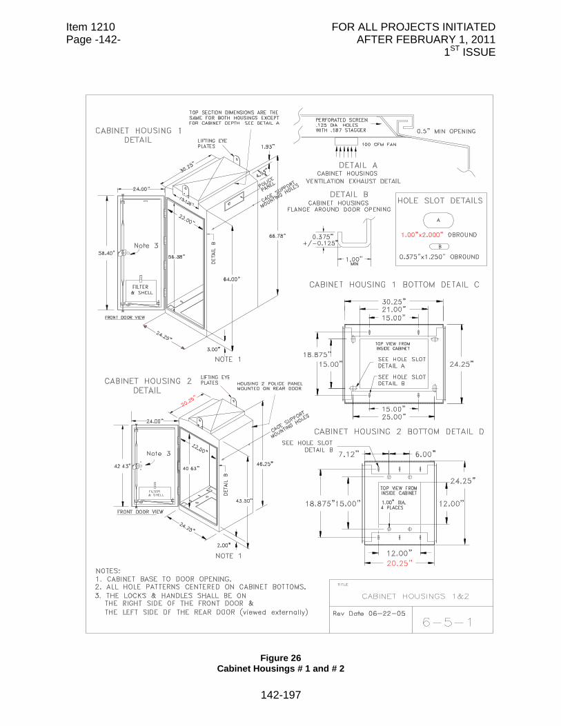
Item 1210 FOR ALL PROJECTS INITIATED Page -142- AFTER FEBRUARY 1, 2011 1ST ISSUE
142-197
Figure 26
Cabinet Housings # 1 and # 2
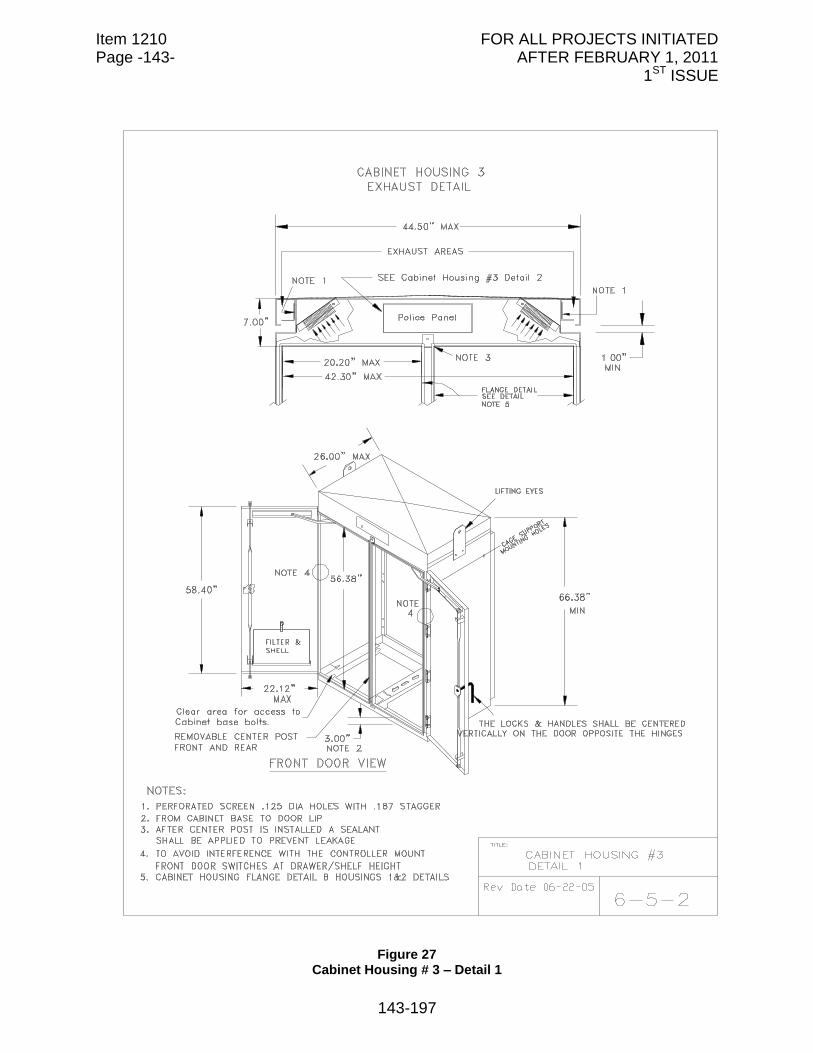
Item 1210 FOR ALL PROJECTS INITIATED Page -143- AFTER FEBRUARY 1, 2011 1ST ISSUE
143-197
Figure 27
Cabinet Housing # 3 – Detail 1
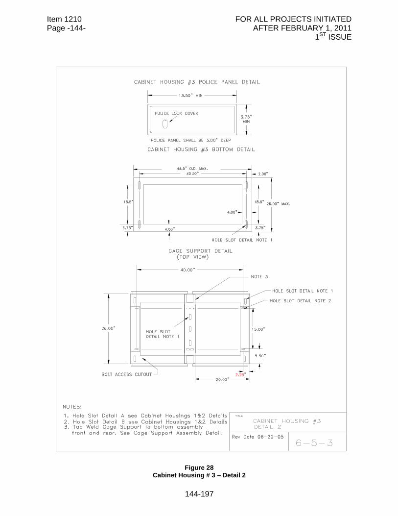
Item 1210 FOR ALL PROJECTS INITIATED Page -144- AFTER FEBRUARY 1, 2011 1ST ISSUE
144-197
Figure 28
Cabinet Housing # 3 – Detail 2
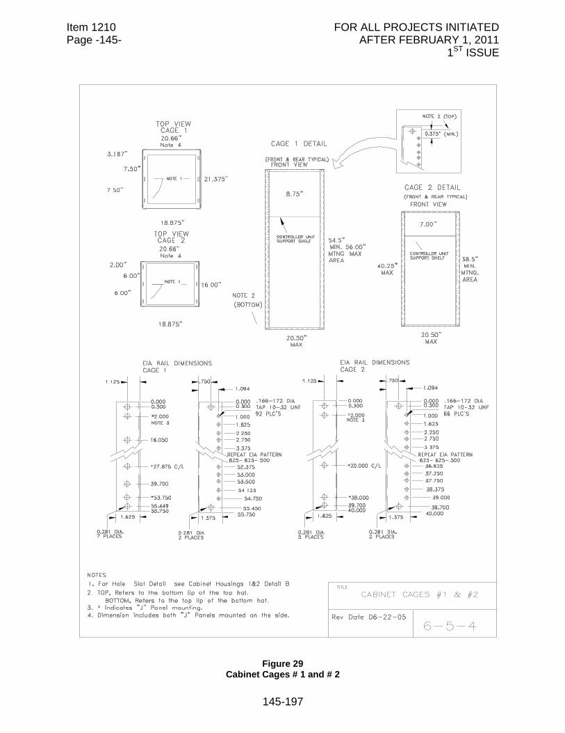
Item 1210 FOR ALL PROJECTS INITIATED Page -145- AFTER FEBRUARY 1, 2011 1ST ISSUE
145-197
Figure 29
Cabinet Cages # 1 and # 2
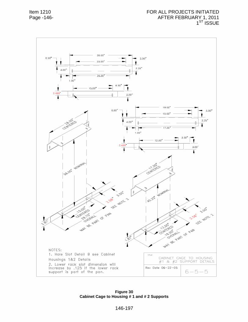
Item 1210 FOR ALL PROJECTS INITIATED Page -146- AFTER FEBRUARY 1, 2011 1ST ISSUE
146-197
Figure 30
Cabinet Cage to Housing # 1 and # 2 Supports
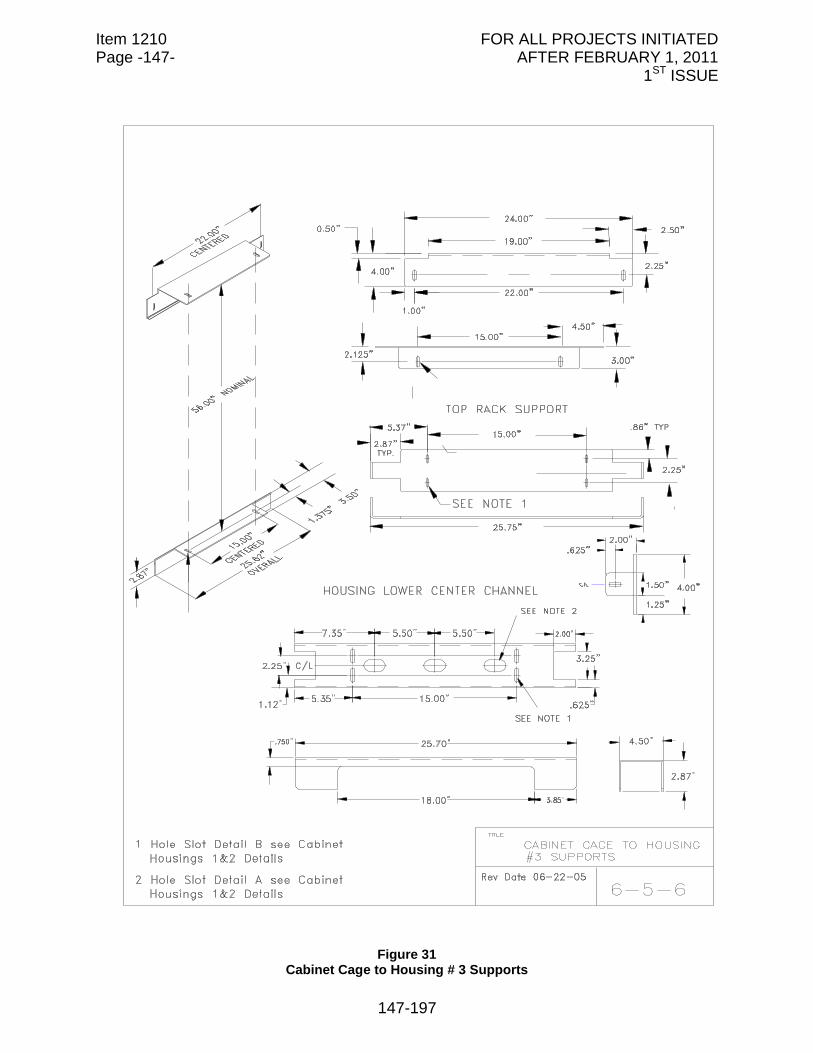
Item 1210 FOR ALL PROJECTS INITIATED Page -147- AFTER FEBRUARY 1, 2011 1ST ISSUE
147-197
Figure 31
Cabinet Cage to Housing # 3 Supports
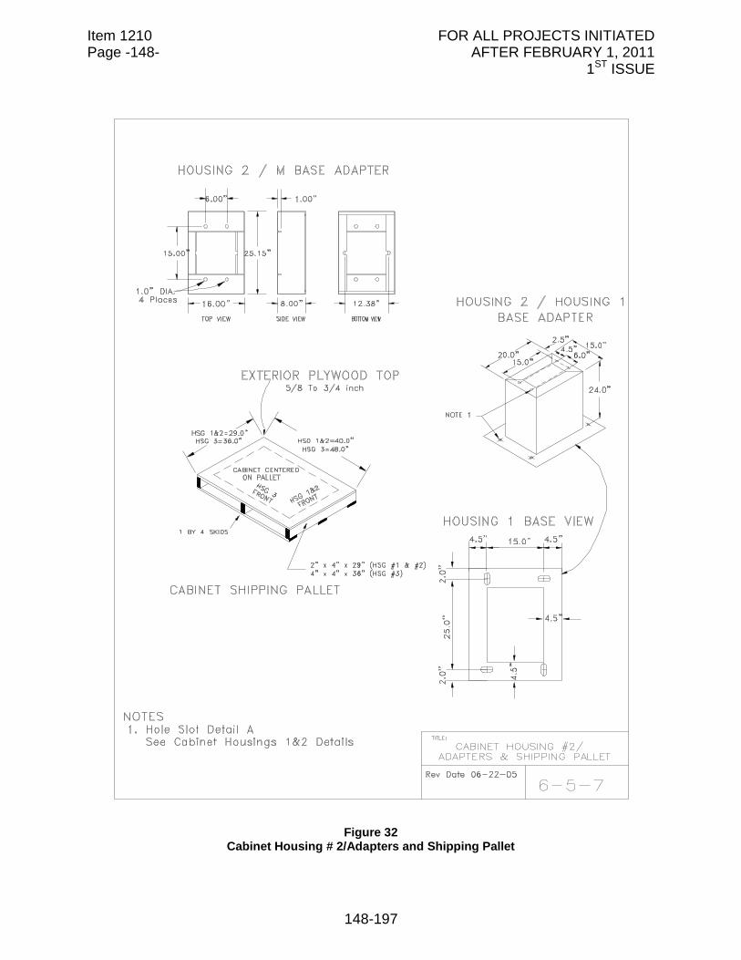
Item 1210 FOR ALL PROJECTS INITIATED Page -148- AFTER FEBRUARY 1, 2011 1ST ISSUE
148-197
Figure 32
Cabinet Housing # 2/Adapters and Shipping Pallet
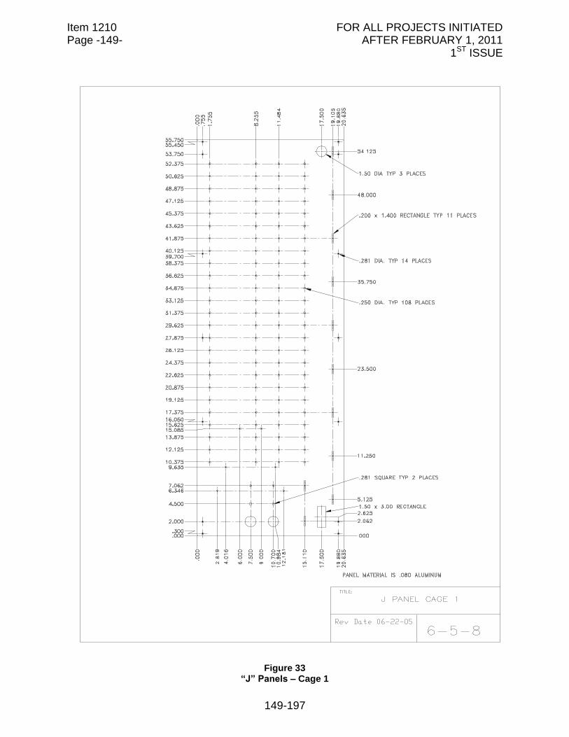
Item 1210 FOR ALL PROJECTS INITIATED Page -149- AFTER FEBRUARY 1, 2011 1ST ISSUE
149-197
Figure 33
“J” Panels – Cage 1
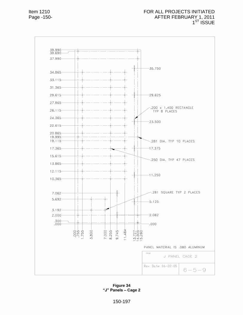
Item 1210 FOR ALL PROJECTS INITIATED Page -150- AFTER FEBRUARY 1, 2011 1ST ISSUE
150-197
Figure 34
“J” Panels – Cage 2
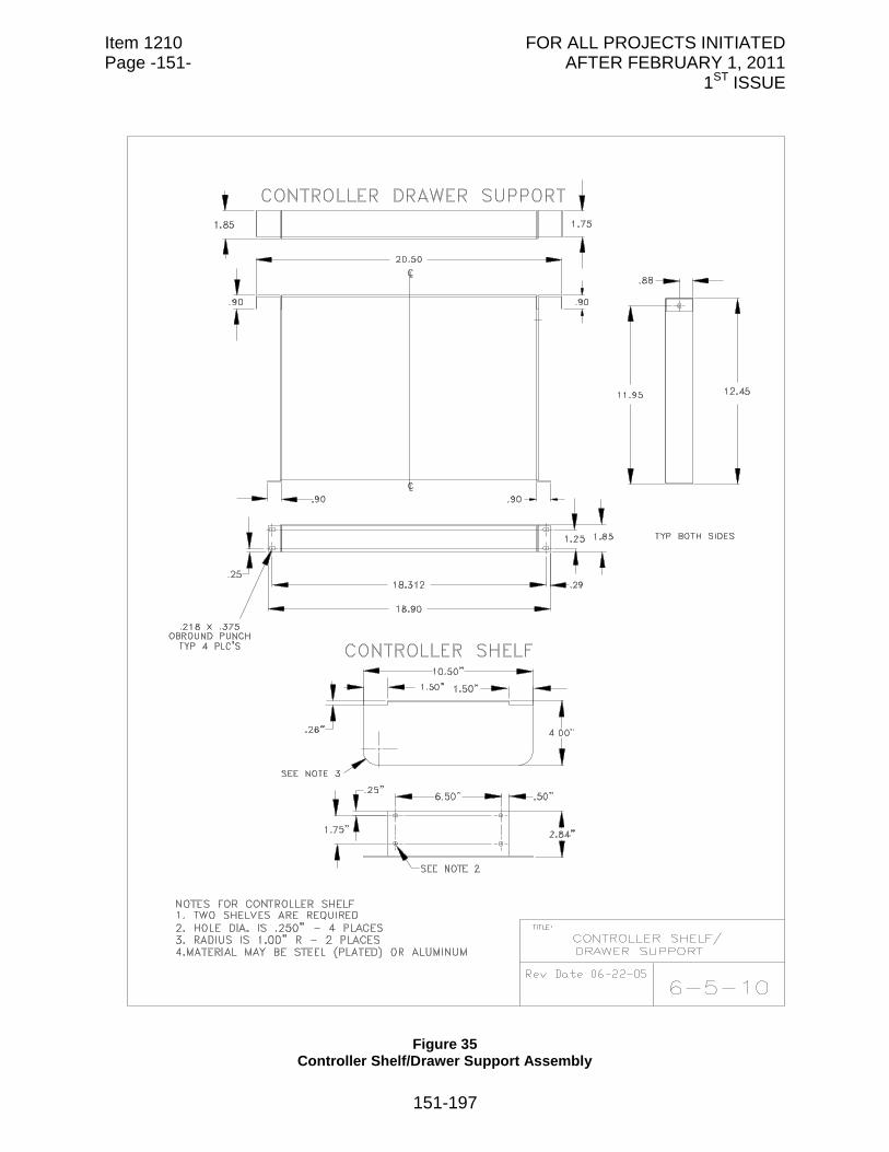
Item 1210 FOR ALL PROJECTS INITIATED Page -151- AFTER FEBRUARY 1, 2011 1ST ISSUE
151-197
Figure 35
Controller Shelf/Drawer Support Assembly
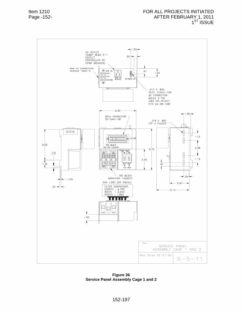
Item 1210 FOR ALL PROJECTS INITIATED Page -152- AFTER FEBRUARY 1, 2011 1ST ISSUE
152-197
Figure 36
Service Panel Assembly Cage 1 and 2
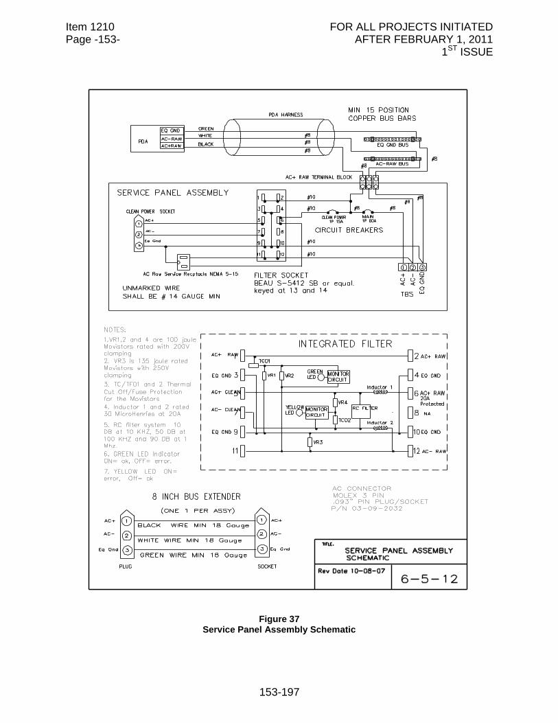
Item 1210 FOR ALL PROJECTS INITIATED Page -153- AFTER FEBRUARY 1, 2011 1ST ISSUE
153-197
Figure 37
Service Panel Assembly Schematic
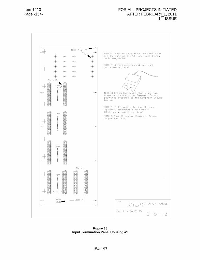
Item 1210 FOR ALL PROJECTS INITIATED Page -154- AFTER FEBRUARY 1, 2011 1ST ISSUE
154-197
Figure 38
Input Termination Panel Housing #1
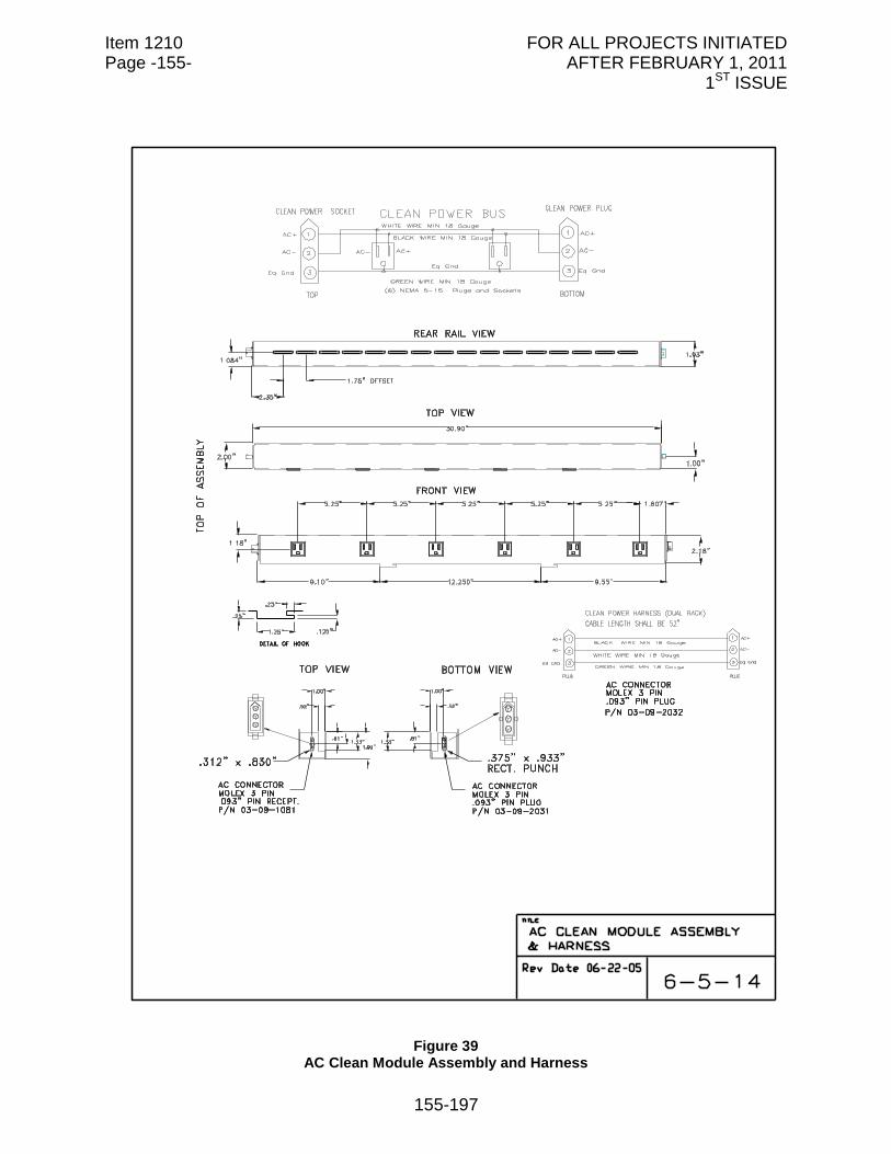
Item 1210 FOR ALL PROJECTS INITIATED Page -155- AFTER FEBRUARY 1, 2011 1ST ISSUE
155-197
Figure 39
AC Clean Module Assembly and Harness
Item 1210 FOR ALL PROJECTS INITIATED Page -156- AFTER FEBRUARY 1, 2011 1ST ISSUE
156-197
Figure 40
Raw/Clean AC Power Assembly and Extension 4 Socket
Item 1210 FOR ALL PROJECTS INITIATED Page -157- AFTER FEBRUARY 1, 2011 1ST ISSUE
157-197
Figure 41
Raw/Clean AC Power Assembly and Extension 2 Socket
Item 1210 FOR ALL PROJECTS INITIATED Page -158- AFTER FEBRUARY 1, 2011 1ST ISSUE
158-197
Figure 42
Raw/Clean AC Power Assembly Wiring Diagram 4 Socket
Item 1210 FOR ALL PROJECTS INITIATED Page -159- AFTER FEBRUARY 1, 2011 1ST ISSUE
159-197
Figure 43
Raw/Clean AC Power Assembly Wiring Diagram 2 Socket
Item 1210 FOR ALL PROJECTS INITIATED Page -160- AFTER FEBRUARY 1, 2011 1ST ISSUE
160-197
Figure 44
DC Power/Communications Assembly and Extension
Item 1210 FOR ALL PROJECTS INITIATED Page -161- AFTER FEBRUARY 1, 2011 1ST ISSUE
161-197
Figure 45
DC Power/Communications Assembly Wiring Diagram
Item 1210 FOR ALL PROJECTS INITIATED Page -162- AFTER FEBRUARY 1, 2011 1ST ISSUE
162-197
Figure 46
PDA 5 IP ITS – Front View
Item 1210 FOR ALL PROJECTS INITIATED Page -163- AFTER FEBRUARY 1, 2011 1ST ISSUE
163-197
Figure 47
PDA 5 EP ITS – Front View
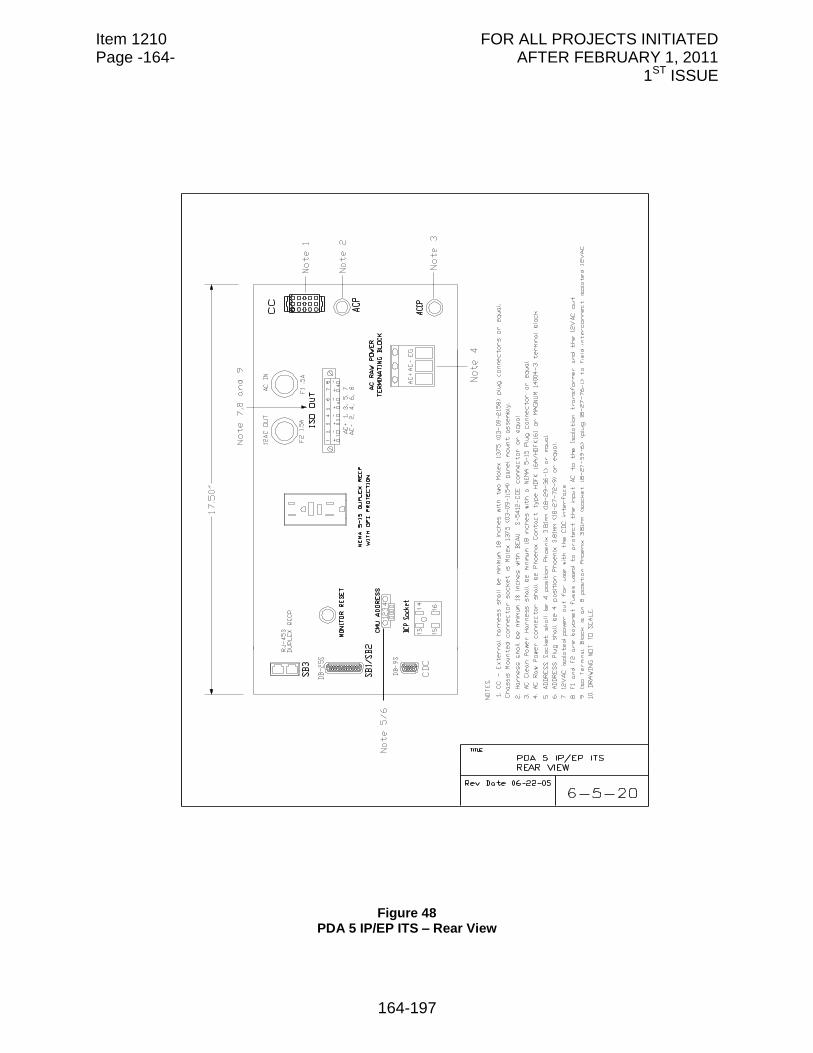
Item 1210 FOR ALL PROJECTS INITIATED Page -164- AFTER FEBRUARY 1, 2011 1ST ISSUE
164-197
Figure 48
PDA 5 IP/EP ITS – Rear View
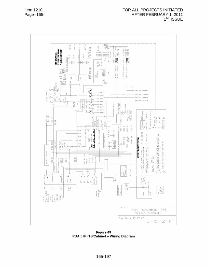
Item 1210 FOR ALL PROJECTS INITIATED Page -165- AFTER FEBRUARY 1, 2011 1ST ISSUE
165-197
Figure 49
PDA 5 IP ITS/Cabinet – Wiring Diagram
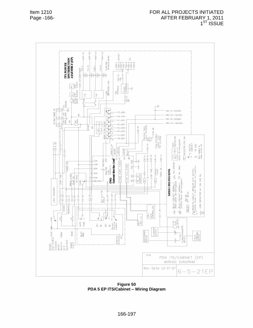
Item 1210 FOR ALL PROJECTS INITIATED Page -166- AFTER FEBRUARY 1, 2011 1ST ISSUE
166-197
Figure 50
PDA 5 EP ITS/Cabinet – Wiring Diagram
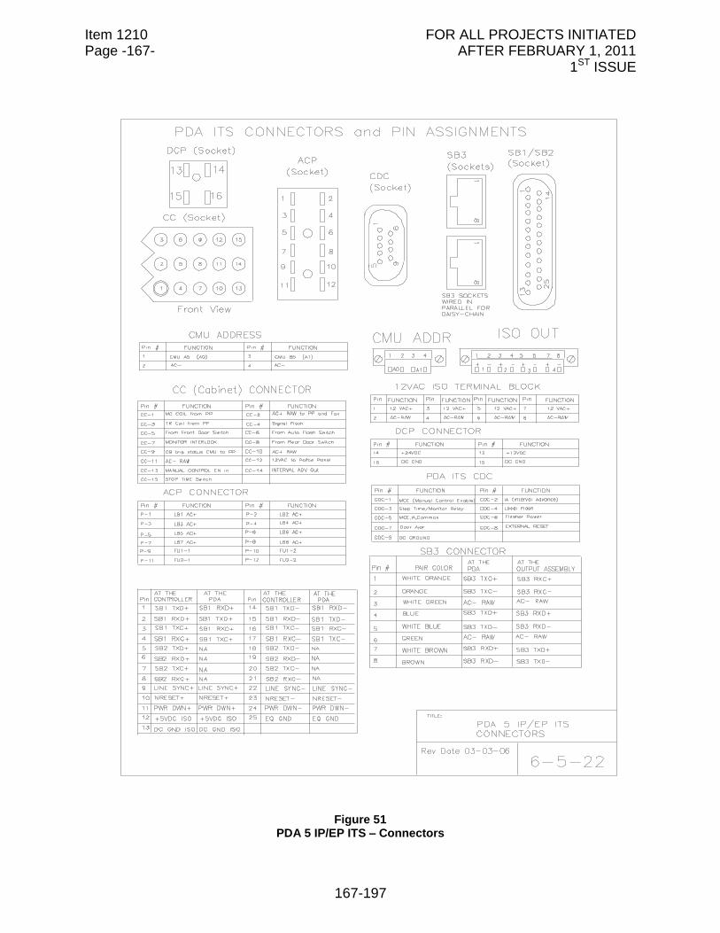
Item 1210 FOR ALL PROJECTS INITIATED Page -167- AFTER FEBRUARY 1, 2011 1ST ISSUE
167-197
Figure 51
PDA 5 IP/EP ITS – Connectors
Item 1210 FOR ALL PROJECTS INITIATED Page -168- AFTER FEBRUARY 1, 2011 1ST ISSUE
168-197
Figure 52
6/14 Pack Output Assembly – Front View
Item 1210 FOR ALL PROJECTS INITIATED Page -169- AFTER FEBRUARY 1, 2011 1ST ISSUE
169-197
Figure 53
6/14 Pack Output Assembly – Rear Views
Item 1210 FOR ALL PROJECTS INITIATED Page -170- AFTER FEBRUARY 1, 2011 1ST ISSUE
170-197
Figure 54
6/14 Pack Output Assembly – Wiring Diagram
Item 1210 FOR ALL PROJECTS INITIATED Page -171- AFTER FEBRUARY 1, 2011 1ST ISSUE
171-197
Figure 55
6 Pack O/A – CB/Flasher Diagram and Assignment Note
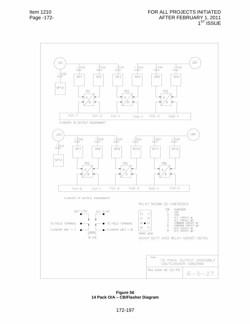
Item 1210 FOR ALL PROJECTS INITIATED Page -172- AFTER FEBRUARY 1, 2011 1ST ISSUE
172-197
Figure 56
14 Pack O/A – CB/Flasher Diagram
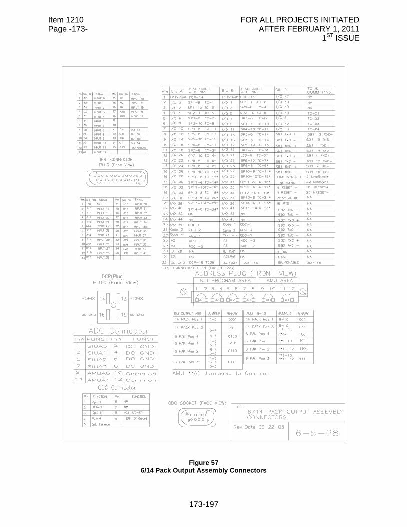
Item 1210 FOR ALL PROJECTS INITIATED Page -173- AFTER FEBRUARY 1, 2011 1ST ISSUE
173-197
Figure 57
6/14 Pack Output Assembly Connectors
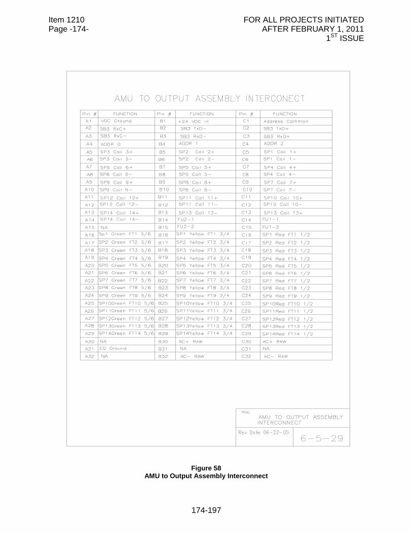
Item 1210 FOR ALL PROJECTS INITIATED Page -174- AFTER FEBRUARY 1, 2011 1ST ISSUE
174-197
Figure 58
AMU to Output Assembly Interconnect
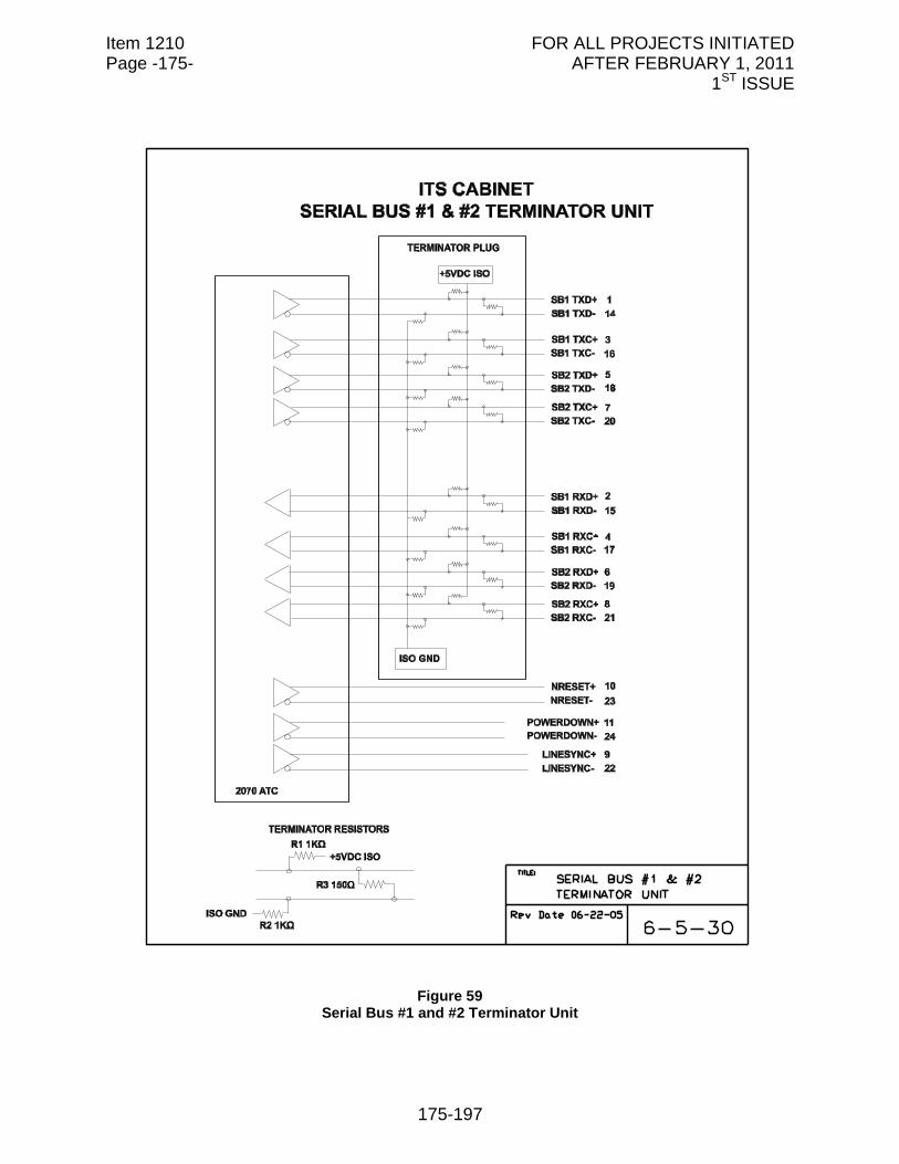
Item 1210 FOR ALL PROJECTS INITIATED Page -175- AFTER FEBRUARY 1, 2011 1ST ISSUE
175-197
Figure 59
Serial Bus #1 and #2 Terminator Unit
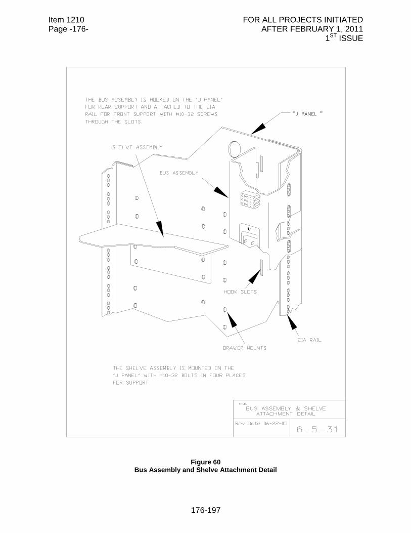
Item 1210 FOR ALL PROJECTS INITIATED Page -176- AFTER FEBRUARY 1, 2011 1ST ISSUE
176-197
Figure 60
Bus Assembly and Shelve Attachment Detail
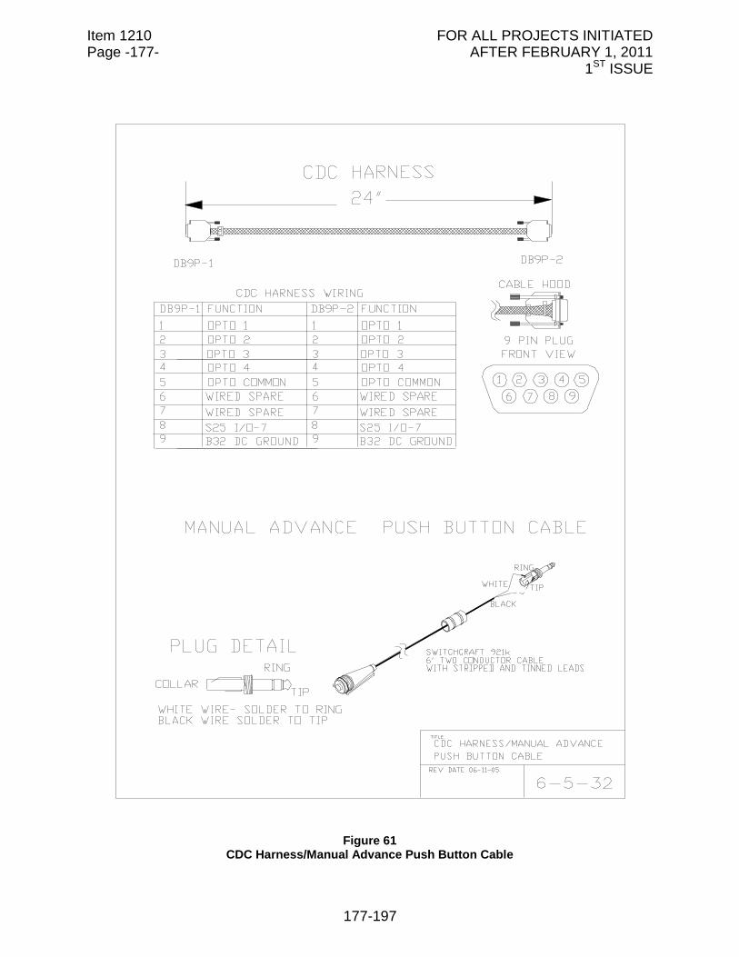
Item 1210 FOR ALL PROJECTS INITIATED Page -177- AFTER FEBRUARY 1, 2011 1ST ISSUE
177-197
Figure 61
CDC Harness/Manual Advance Push Button Cable

Item 1210 FOR ALL PROJECTS INITIATED Page -178- AFTER FEBRUARY 1, 2011 1ST ISSUE
178-197
This page intentionally left blank.
Figure 62 RESERVED

Item 1210 FOR ALL PROJECTS INITIATED Page -179- AFTER FEBRUARY 1, 2011 1ST ISSUE
179-197
This page intentionally left blank.
Figure 63 RESERVED
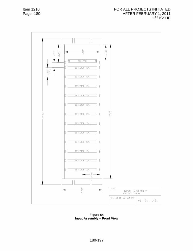
Item 1210 FOR ALL PROJECTS INITIATED Page -180- AFTER FEBRUARY 1, 2011 1ST ISSUE
180-197
Figure 64
Input Assembly – Front View
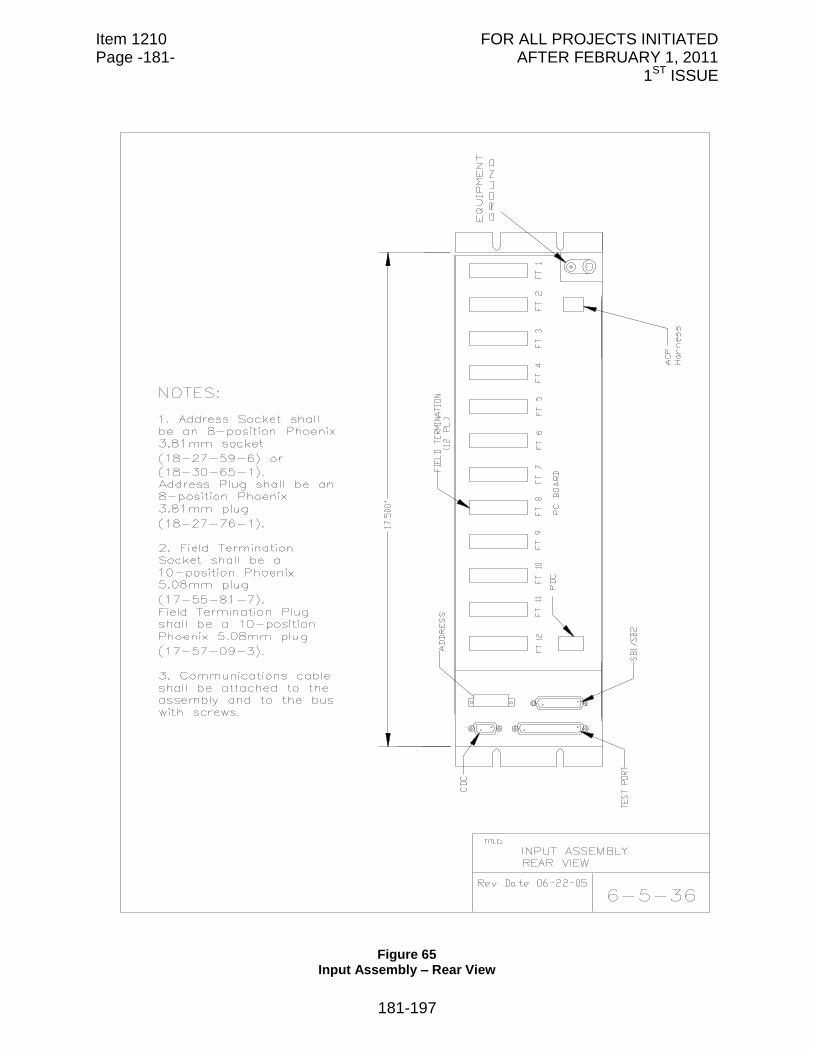
Item 1210 FOR ALL PROJECTS INITIATED Page -181- AFTER FEBRUARY 1, 2011 1ST ISSUE
181-197
Figure 65
Input Assembly – Rear View
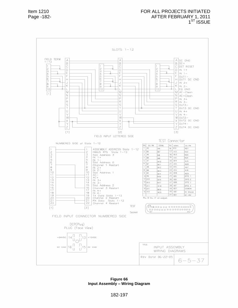
Item 1210 FOR ALL PROJECTS INITIATED Page -182- AFTER FEBRUARY 1, 2011 1ST ISSUE
182-197
Figure 66
Input Assembly – Wiring Diagram
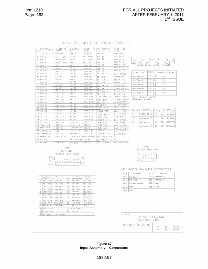
Item 1210 FOR ALL PROJECTS INITIATED Page -183- AFTER FEBRUARY 1, 2011 1ST ISSUE
183-197
Figure 67
Input Assembly – Connectors
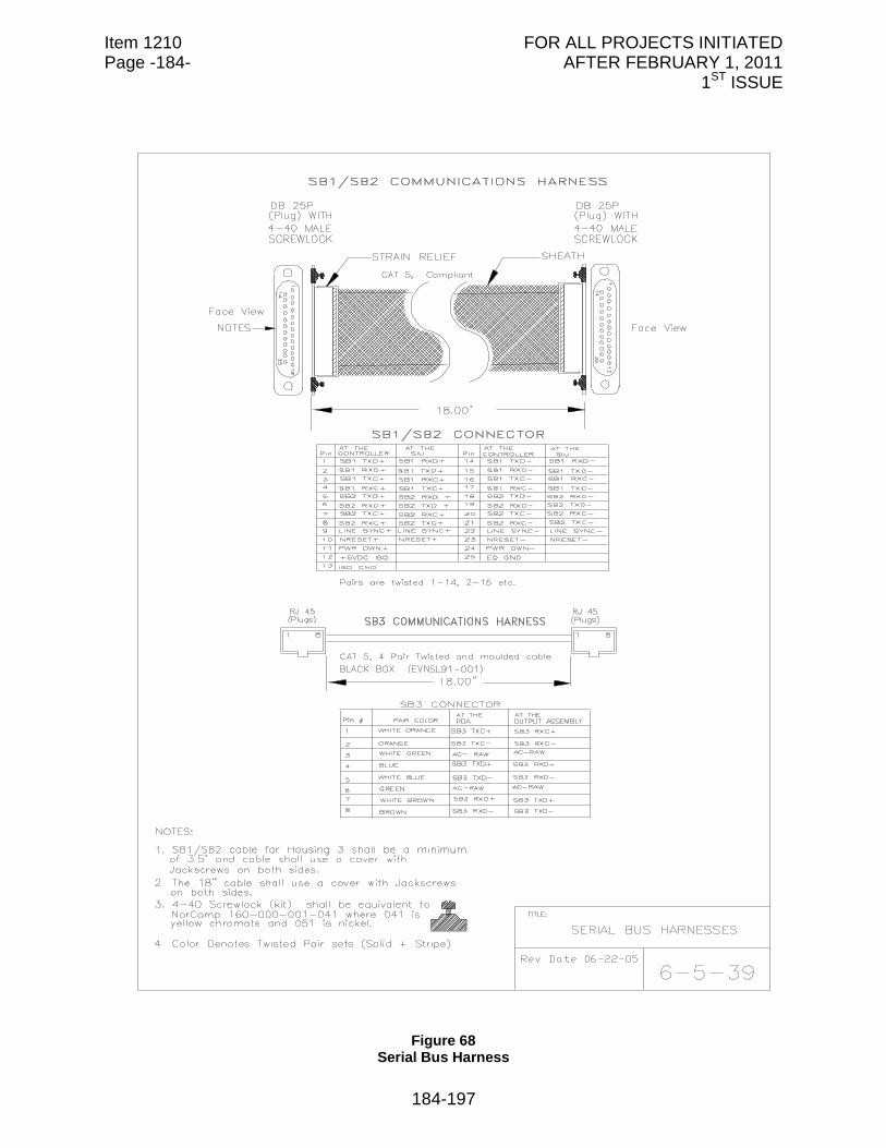
Item 1210 FOR ALL PROJECTS INITIATED Page -184- AFTER FEBRUARY 1, 2011 1ST ISSUE
184-197
Figure 68
Serial Bus Harness
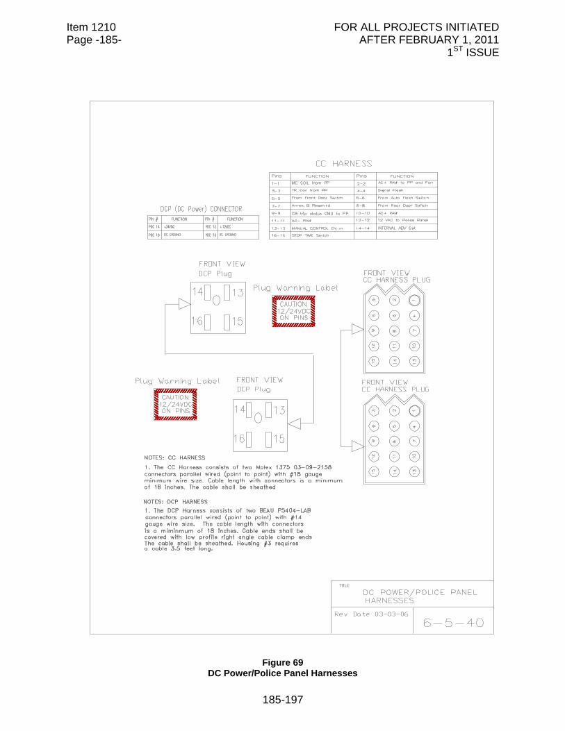
Item 1210 FOR ALL PROJECTS INITIATED Page -185- AFTER FEBRUARY 1, 2011 1ST ISSUE
185-197
Figure 69
DC Power/Police Panel Harnesses
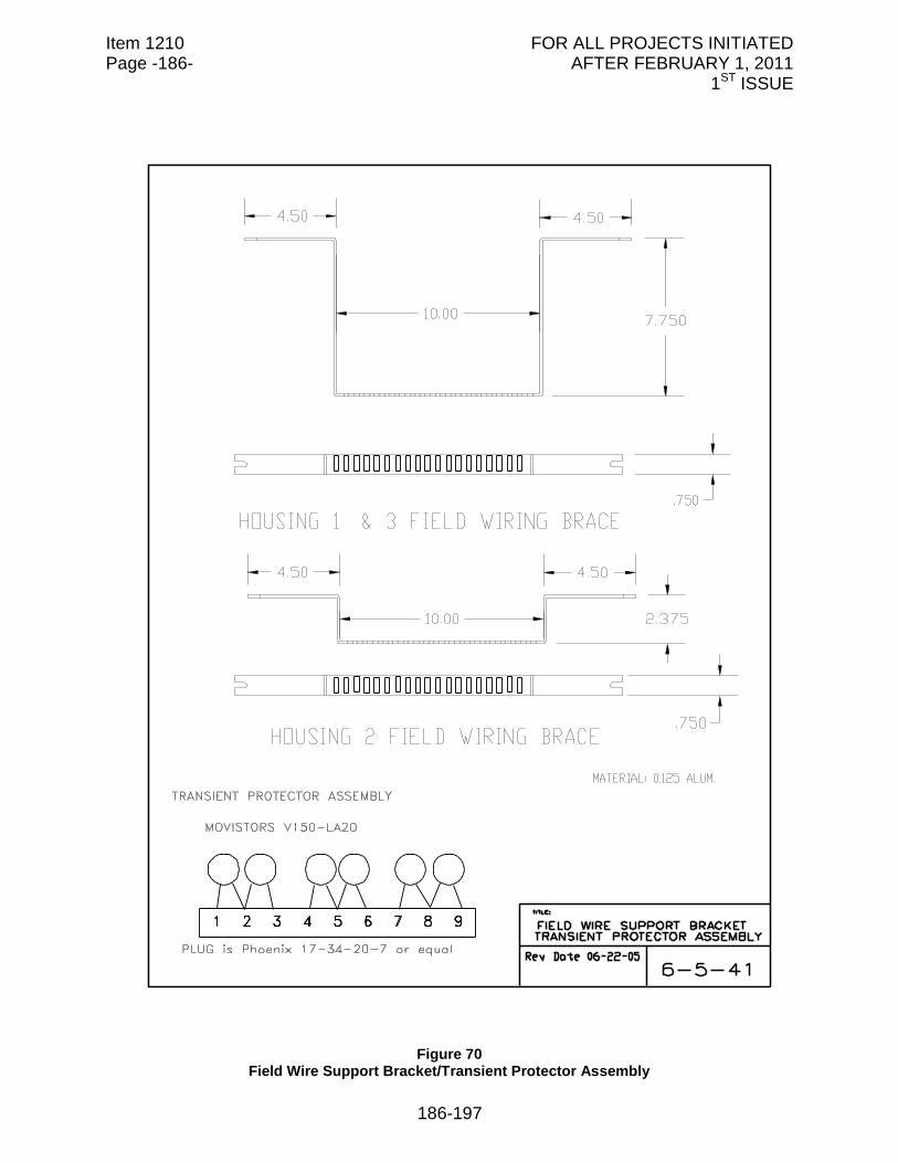
Item 1210 FOR ALL PROJECTS INITIATED Page -186- AFTER FEBRUARY 1, 2011 1ST ISSUE
186-197
Figure 70
Field Wire Support Bracket/Transient Protector Assembly
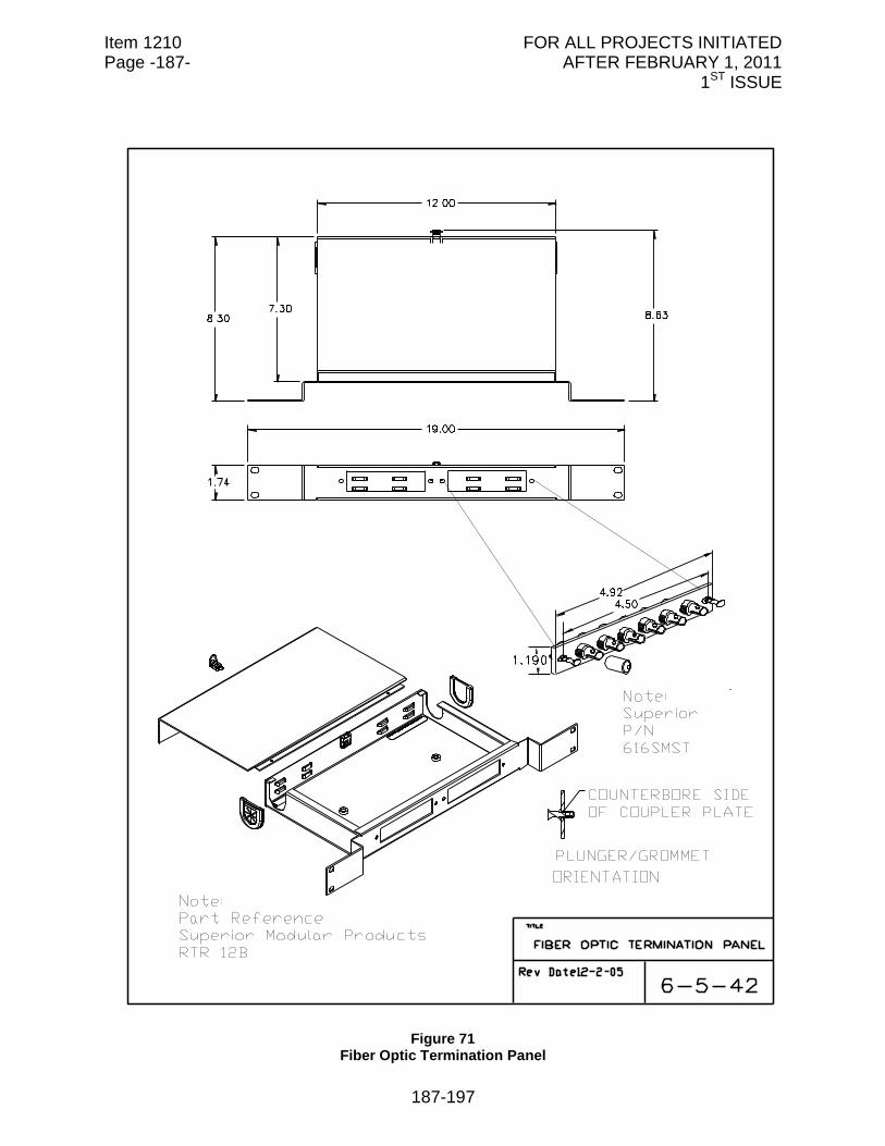
Item 1210 FOR ALL PROJECTS INITIATED Page -187- AFTER FEBRUARY 1, 2011 1ST ISSUE
187-197
Figure 71
Fiber Optic Termination Panel
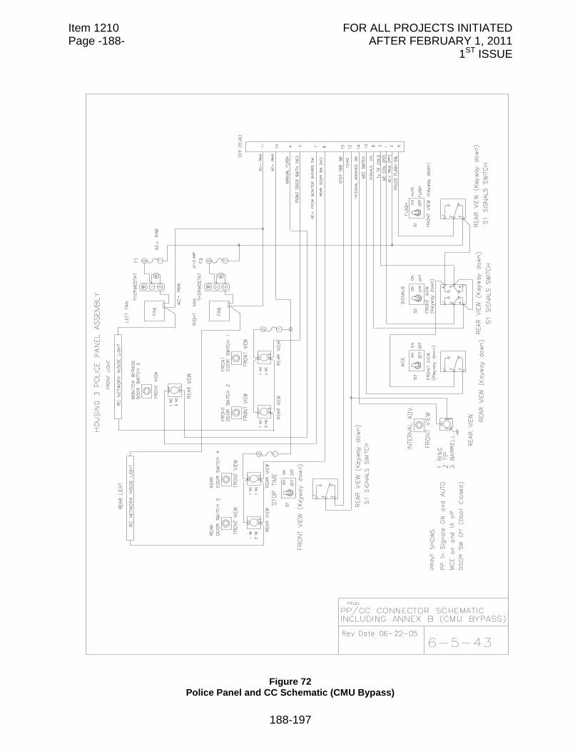
Item 1210 FOR ALL PROJECTS INITIATED Page -188- AFTER FEBRUARY 1, 2011 1ST ISSUE
188-197
Figure 72
Police Panel and CC Schematic (CMU Bypass)
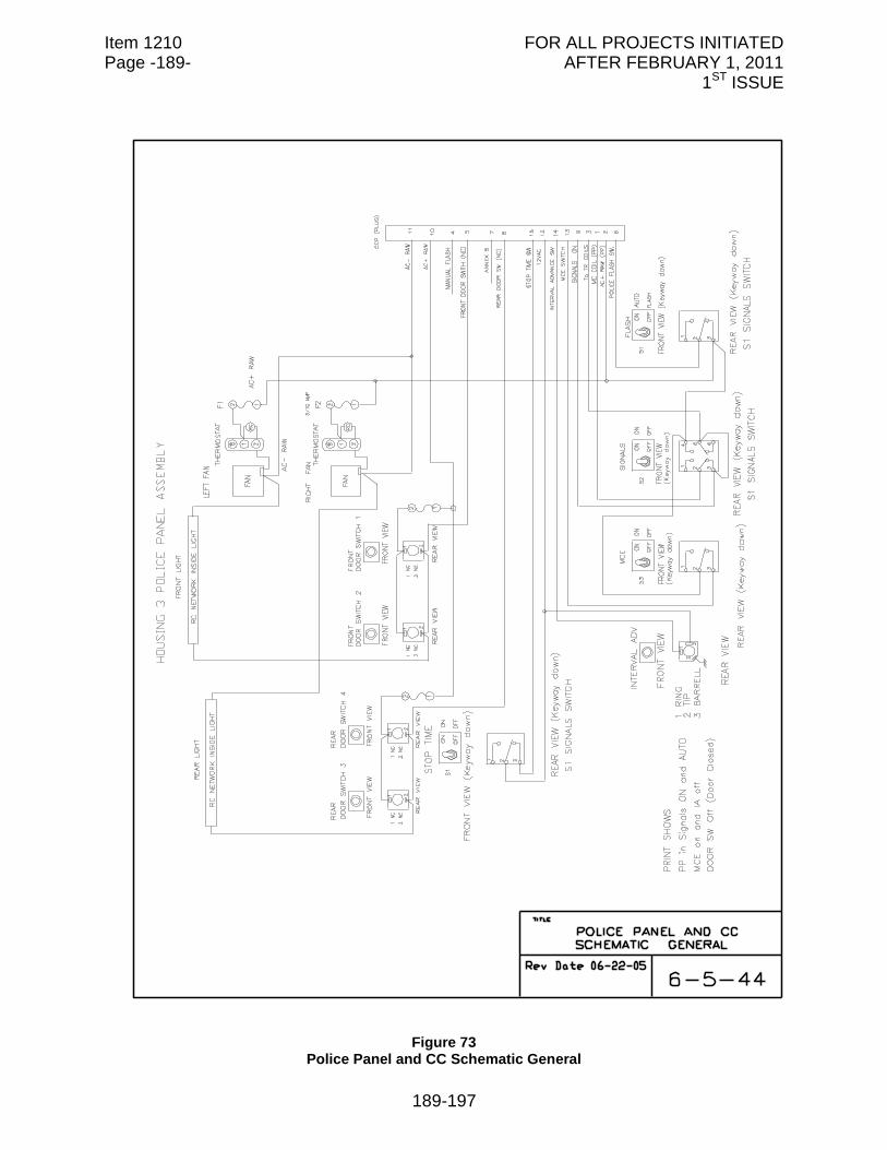
Item 1210 FOR ALL PROJECTS INITIATED Page -189- AFTER FEBRUARY 1, 2011 1ST ISSUE
189-197
Figure 73
Police Panel and CC Schematic General
Item 1210 FOR ALL PROJECTS INITIATED Page -190- AFTER FEBRUARY 1, 2011 1ST ISSUE
190-197
13. Glossary.
A. Terms and Abbreviations. Wherever the following terms or abbreviations are used, the intent and meaning is interpreted as follows:
A Ampere
AC Alternating Current
AC+ 120 Volts AC, 60 hertz ungrounded power source
AC- 120 Volts AC, 60 hertz grounded return to the power source
AGENCY The AGENCY director, acting either directly or through properly authorized agents, such agents acting within the scope of the particular duties delegated to them.
ANSI American National Standard Institute
ASCII American Standard Code for Information Interchange
Assembly A complete machine, structure or unit of a machine that was manufactured by fitting together parts and/or modules
ASTM American Society for Testing and Materials
AWG American Wire Gage
C Celsius
C Language The ANSI C Programming Language
Cabinet An outdoor enclosure generally housing the controller unit and associated equipment
Certificate of Compliance A certificate signed by the manufacturer of the material or the manufacturer of assembled materials stating that the materials involved comply in all respects with the requirements of the specifications
Item 1210 FOR ALL PROJECTS INITIATED Page -191- AFTER FEBRUARY 1, 2011 1ST ISSUE
191-197
Channel An information path from a discrete input to a discrete output.
Component Any electrical or electronic device
Contractor The person or persons, Manufacturer, firm, partnership, corporation, vendor or combination thereof, who have entered into a contract with the AGENCY, as party of the second part or legal representative
Controller Unit That portion of the controller assembly devoted to the operational control of the logic decisions programmed into the assembly
CPU Central Processing Unit
CTS Clear To Send
DAT Program The AGENCY’s Diagnostic and Acceptance Test Program
dB Decibel
dBa Decibels above reference noise, adjusted
DC Direct Current
DCD Data Carrier Detect (Receive Line Signal Detector)
DIN Deutsche Industrie Norm
DRAM Dynamic random access memory. Random access means that the processor can access any part of the memory or data storage space directly rather than having to proceed sequentially from some starting place. DRAM is dynamic in that it needs to have its storage cells refreshed or given a new electronic charge every few milliseconds.
EG Equipment Ground
EIA Electronic Industries Association
EMI Electro Magnetic Interference
Item 1210 FOR ALL PROJECTS INITIATED Page -192- AFTER FEBRUARY 1, 2011 1ST ISSUE
192-197
EPROM Ultraviolet Erasable, Programmable, Read Only Memory Device
EEPROM Electrically Erasable, Programmable, Read Only Memory Device
Equal Connectors: comply with physical dimensions, contact material, plating and method of connection. Devices: comply to function, pin out, electrical and operating parameter requirements, access times and interface parameters of the specified device
ETL Electrical Testing Laboratories, Inc.
Firmware A computer program or software stored permanently in PROM, EPROM, ROM or semi-permanently in EEPROM
FLASH A +5 VDC powered IC Memory Device with nonvolatile, electrically erasable, programmable, 100K read/write minimum cycles and fast access time features
FPA Front Panel Assembly
HEX Hexadecimal
Hz Hertz
IC Integrated Circuit
I.D. Identification
IEEE Institute of Electrical and Electronics Engineers
ISO Isolated
Jumper A means of connecting/disconnecting two or more conductive by soldering/desoldering a conductive wire or by PCB post jumper
KB Kilobytes
Item 1210 FOR ALL PROJECTS INITIATED Page -193- AFTER FEBRUARY 1, 2011 1ST ISSUE
193-197
Keyed Means by which like connectors can be physically altered to prevent improper insertion.
Laboratory The established laboratory of the AGENCY or other laboratories authorized by the AGENCY to test materials involved in the contract
LCD Liquid Crystal Display
LED Light Emitting Diode
LOGIC Negative Logic Convention (Ground True) State
LSB Least Significant Byte
lsb Least Significant Bit
MB megabyte
MSB Most Significant Byte
msb Most Significant Bit
m Milli
MCU/MPU/ IMP Micro Controller Unit, Microprocessor Unit, or Integrated Multiprotocol Processor
MIL Military Specifications
MODEM Modulation/Demodulation Unit
Module A functional unit that plugs into an assembly
Motherboard A printed circuit connector interface board with no active or passive components
MOS Metal-Oxide Semiconductor
MOV Metal-Oxide Varistor
MS Military Standards
Item 1210 FOR ALL PROJECTS INITIATED Page -194- AFTER FEBRUARY 1, 2011 1ST ISSUE
194-197
N Newton: SI unit of force
N.C. Normally closed contact
N.O. Normally open contact
NA Presently Not Assigned. Cannot be used by the Manufacturer for other purposes
NEMA National Electrical Manufacturer's Association
NETA National Electrical Testing Association, Inc.
n nano
NLSB Next Least Significant Byte
nlsb Next Least Significant Bit
NMSB Next Most Significant Byte
nmsb Next Most Significant Bit
PCB Printed Circuit Board
PDA Power Distribution Assembly
PLA/PAL Programmable Array Logic Device
Power Failure A Power Failure is said to have occurred when the incoming line voltage falls below 92 +/- 2 VAC for 50 milliseconds. See Power Conditions.
Power Restoration Power is said to be restored when the incoming line voltage equals or exceeds 97 +/- 2 VAC for 50 milliseconds. See Power Conditions.
Power Conditions 16.7 ms (one 60 Hertz cycle) reaction period is allowed to be included in the 50 milliseconds timing or added to (67 milliseconds duration). The hysteresis between power failure and
Item 1210 FOR ALL PROJECTS INITIATED Page -195- AFTER FEBRUARY 1, 2011 1ST ISSUE
195-197
power restoration voltage settings must be a min. of 5 VAC with a threshold drift of no more than 0.2 VAC.
ppm Parts per million
PWM Pulse Width Modulation
RAM Random Access Memory
RF Radio Frequency
RMS Root-Mean-Square
ROM Read Only Memory Device
RTS Request to Send
R/W Controller Unit Read/Write Control Line
RxD Received Data
SCI Serial Communications Interface
SDLC Synchronous Data Link Control
S Logic State
s second
Second Sourced Produced by more than one Manufacturer
SRAM Static Random Access Memory Device
SW Switch
TB Terminal Block
TOD Time Of Day Clock
Triac Silicon-Controlled Rectifier which controls power bilaterally in an AC switching circuit

Item 1210 FOR ALL PROJECTS INITIATED Page -196- AFTER FEBRUARY 1, 2011 1ST ISSUE
196-197
TTL Transistor-Transistor Logic
Thumb Screw Device (TSD ) A retractable screw fastener with projecting stainless steel screw, spring and natural aluminum knob finish. (TSD No.2 must be flat black.)
TSD No.1 - 8-32 SOUTHCO #47-62-301-20 or equal. TSD No.2 - 8-32 SOUTHCO #47-62-301-60 or equal. TSD No.3 - M3 SOUTHCO #47-82-101-10 or equal.
TxD Transmitted Data
u Micro
UL Underwriter's Laboratories, Inc.
VAC Voltage Alternating Current (root mean square)
VDC Voltage Direct Current
VME Versa Module Eurocard, VMEbus Standard IEEE P1014/D1.2
x Number Value
XX Manufacturer's Option
WDT Watchdog Timer: A monitoring circuit, external to the device watched, which senses an Output Line from the device and reacts
14. Legacy Device Implementation. A prototyping effort was conducted along with the development of this ITS Cabinet Standard. During the early stages of the prototyping effort, there were no SIU, AMU, and CMU devices available. As a result, a C1 and C11 interconnect list was developed to establish a method for using legacy 2070 controller applications. The list was developed with the Caltrans Model 332 and Model 336 Housing 2 Cabinets in mind. ITS Cabinet Housing #3 (with two internal racks) was the target prototype model being deployed in Harris County Texas, Housing 1 and Housing 2 ITS Cabinets have been deployed in small numbers.
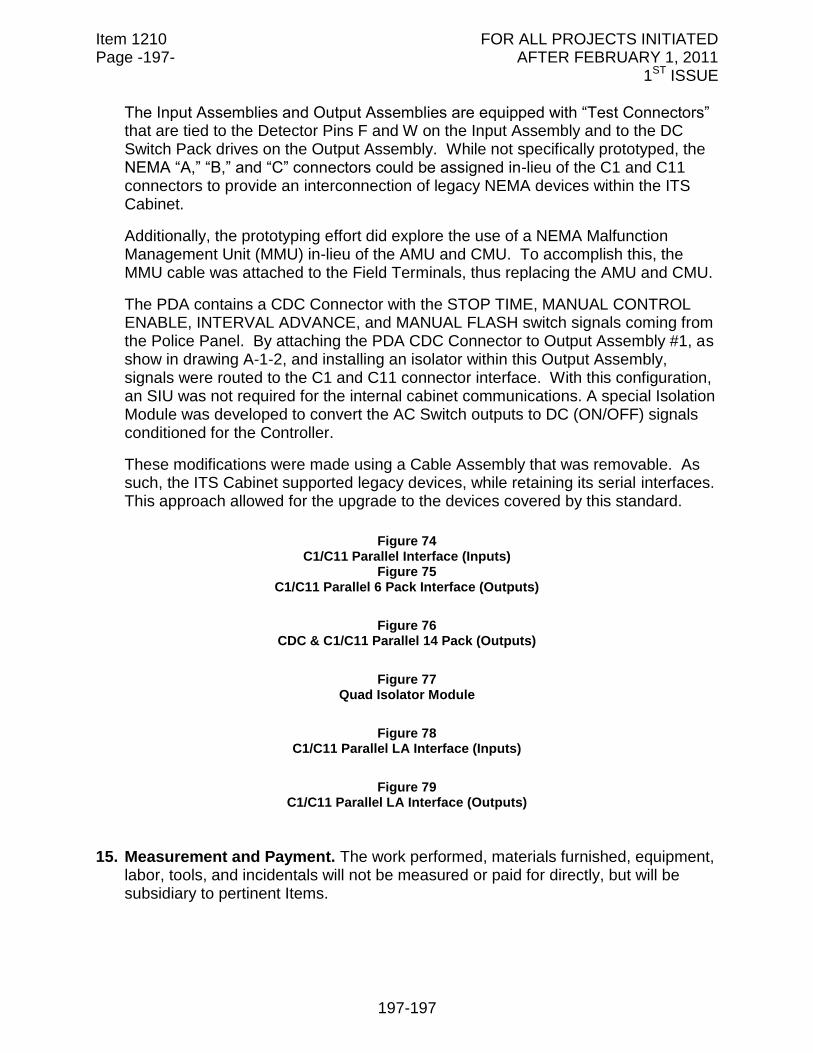
Item 1210 FOR ALL PROJECTS INITIATED Page -197- AFTER FEBRUARY 1, 2011 1ST ISSUE
197-197
The Input Assemblies and Output Assemblies are equipped with “Test Connectors” that are tied to the Detector Pins F and W on the Input Assembly and to the DC Switch Pack drives on the Output Assembly. While not specifically prototyped, the NEMA “A,” “B,” and “C” connectors could be assigned in-lieu of the C1 and C11 connectors to provide an interconnection of legacy NEMA devices within the ITS Cabinet.
Additionally, the prototyping effort did explore the use of a NEMA Malfunction Management Unit (MMU) in-lieu of the AMU and CMU. To accomplish this, the MMU cable was attached to the Field Terminals, thus replacing the AMU and CMU.
The PDA contains a CDC Connector with the STOP TIME, MANUAL CONTROL ENABLE, INTERVAL ADVANCE, and MANUAL FLASH switch signals coming from the Police Panel. By attaching the PDA CDC Connector to Output Assembly #1, as show in drawing A-1-2, and installing an isolator within this Output Assembly, signals were routed to the C1 and C11 connector interface. With this configuration, an SIU was not required for the internal cabinet communications. A special Isolation Module was developed to convert the AC Switch outputs to DC (ON/OFF) signals conditioned for the Controller.
These modifications were made using a Cable Assembly that was removable. As such, the ITS Cabinet supported legacy devices, while retaining its serial interfaces. This approach allowed for the upgrade to the devices covered by this standard.
Figure 74
C1/C11 Parallel Interface (Inputs) Figure 75
C1/C11 Parallel 6 Pack Interface (Outputs)
Figure 76
CDC & C1/C11 Parallel 14 Pack (Outputs)
Figure 77
Quad Isolator Module
Figure 78
C1/C11 Parallel LA Interface (Inputs)
Figure 79
C1/C11 Parallel LA Interface (Outputs)
15. Measurement and Payment. The work performed, materials furnished, equipment, labor, tools, and incidentals will not be measured or paid for directly, but will be subsidiary to pertinent Items.