Embed Size (px)
Citation preview
- 1 -
IWILL DX400-SN (Version 1.2A) High-End Workstation Motherboard User's Manual
FB11360030000
- 2 -
Contents
Motherboard Description 1. Overview… … … … … … … … … … … … … … … … … … … … … … … … … … … ..… … … … 4
Feature Summary Manufacturing Options
2. Motherboard Layout… … … … … … … … … … … … … … … … … … … … … … … … … ...6 Supported Processors Installing the Processors Installing the Retention Mechanism
3. System Memory… … … … … … … … … … ..… … … … … … … … … … … … … … … … ...12 MEC on motherboard MEC8 Usage ECC Memory Memory Installation
4. Intel 860 Chipset… … … … … … … … … … … … … … … … … … … … … … … … … … … .17 AGP & AGP Pro50 USB IDE RTC, CMOS SRAM and Battery
5. I/O Controller… … … … … … … … … … … … … … … … … … … … … … … … … … … … ..21 Serial Port Infrared Support Parallel Port Diskette Driver Controller Keyboard and Mouse Interface
6. Audio Subsystem… … … … … … … … … … … … … … … … … … … … … … … … … … ..23 Audio Codec Audio Connectors CD-ROM audio mixer connector ATAPI-style telephony connector
7. Hardware Management Features… … … … … … … … … … … … … … … … … … … ..25 Hardware Monitor Subsystem Chassis Intrusion Detection Connectors Fan control and Monitoring
8. Power Management Features… … … … … … … … … … … … … … … … … … … … … 27 Software Support of ACPI Hardware Support Power Connectors
- 3 -
Fan Connectors AOL2 Technology Wake on Lan Technology Wake on Ring Technology Wake on USB
9. LAN subsystem… … … … … … … … … … … … … … … … … … … … … … … … … … … ..30 Intel 82550 Lan Controller Alert On LAN Component LAN subsystem software RJ-45 LAN connector LEDs
10. Jumper Setting & Connector… … … … … … … … … .… … … … … … … … … … … … .32 Back Panel Connector FAN Connectors Peripheral Connector Front Panel Connectors Jumper Setting Thermal Sensor Connector Specification
11. BIOS Setup… … … … … … … … … … … … … .… … … … … … … … … … … … … .… … … .42 BIOS Introduction
Main Menu Standard CMOS Features Advanced Boot Features Advanced Chipset Features Integrated Peripherals Power Management Setup PnP/PCI Configurations Security Features CPU Smart Setting PC Health Status
12. Fast!UTIL (On-Board SCSI BIOS Utility)… … … … … … … … … … … .… … … … … .58 Configuration Settings Scan SCSI Bus SCSI Disk Utility Select Host Adapter Exit Fast!UTIL
13. Appendix… … … … … .… … … … … … … … … … … … … … … … … … … … … … … … … ..62 Beep Codes BIOS Protection/Auto Recovery Feature AWARD BIOS POST CONTROL FLOW
- 4 -
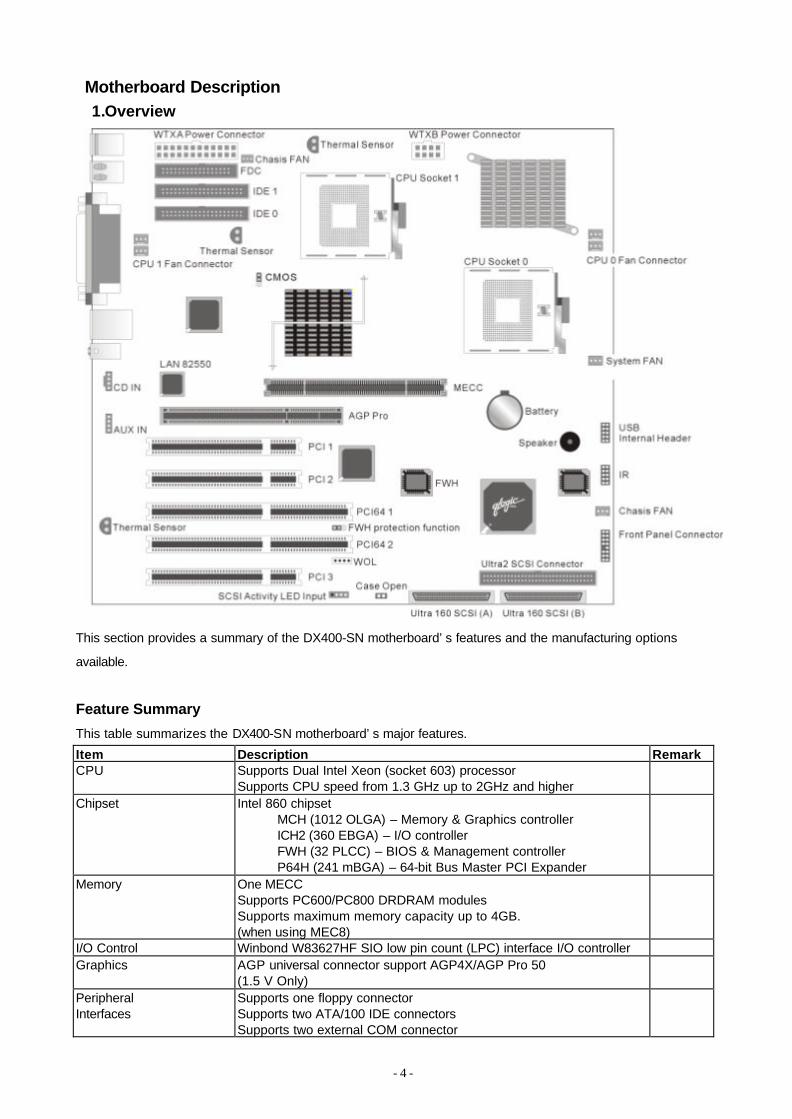
Motherboard Description 1.Overview
This section provides a summary of the DX400-SN motherboard’s features and the manufacturing options
available.
Feature Summary
This table summarizes the DX400-SN motherboard’s major features.
Item Description Remark CPU Supports Dual Intel Xeon (socket 603) processor
Supports CPU speed from 1.3 GHz up to 2GHz and higher
Chipset Intel 860 chipset MCH (1012 OLGA) – Memory & Graphics controller ICH2 (360 EBGA) – I/O controller FWH (32 PLCC) – BIOS & Management controller P64H (241 mBGA) – 64-bit Bus Master PCI Expander
Memory One MECC Supports PC600/PC800 DRDRAM modules Supports maximum memory capacity up to 4GB. (when using MEC8)
I/O Control Winbond W83627HF SIO low pin count (LPC) interface I/O controller Graphics AGP universal connector support AGP4X/AGP Pro 50
(1.5 V Only)
Peripheral Interfaces
Supports one floppy connector Supports two ATA/100 IDE connectors Supports two external COM connector
- 5 -
Supports one external Parallel connector Supports four external USB 1.1 connectors Supports two internal USB 1.1 connectors Supports one external PS/2 keyboard connector Supports one external PS/2 mouse connector Supports one Front-Panel connector
PCI Supports three 32-bit/33MHz Bus Master PCI slot Supports two 64-bit/66MHz Bus Master PCI slots
H/W Monitoring Supports Voltage sense to detect out of range values Supports three Fan Speed Monitoring and Control Supports three Temperature Monitoring Supports Chassis Intrusion detection.
Management Resume by LAN/Ext. Modem/PS2 keyboard/PS2 mouse/RTC Supports Intel LDCM/LDSM (optional) Supports ACPI Supports APM Supports SMBUS Supports DMI Supports PnP Supports BIOS Flash Control to provide H/W & S/W BIOS protection Supports AC-Loss Recovery
Software Focus on the Windows NT 4.0/Windows 2000/Redhat Linux Corelogic Patch utility for Windows 2000(T.B.D.) SCSI Driver Set for Windows NT 4.0/Windows 2000/Redhat Linux H/W Monitoring utility for Windows NT 4.0/Windows 2000(T.B.D.)
Power Supply Limitation Supports WTX power connectors only Misc. On-board Buzzer
8-layer PCB design ATX form-factor with 305mm x330mm board size
Specifications - Optional Components
The following on-board components are optional at the time of purchase:
Please contact with IWILL to determine which options are available to you.
Options Audio Audio Codec’97 (AD1881A) compatible using an AD1881
audio codec LAN Support for LAN on motherboard
* Intel 82550 Local Area Network (LAN) Controller * Alert on LAN 2 device * RJ45 LAN connector
Qlogic Ultra 160 SCSI Controller
Support three SCSI Interface Onboard * Two 68pin SCSI connector * One 50pin SCSI connector
- 6 -
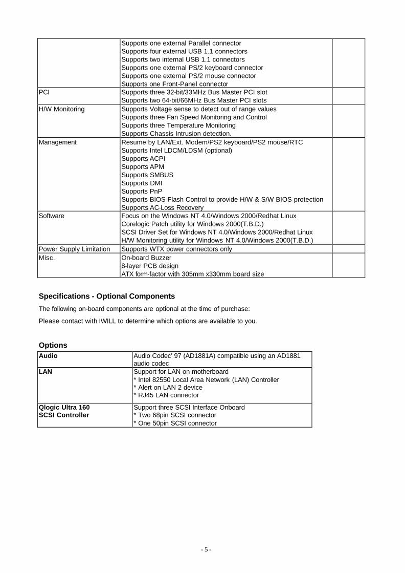
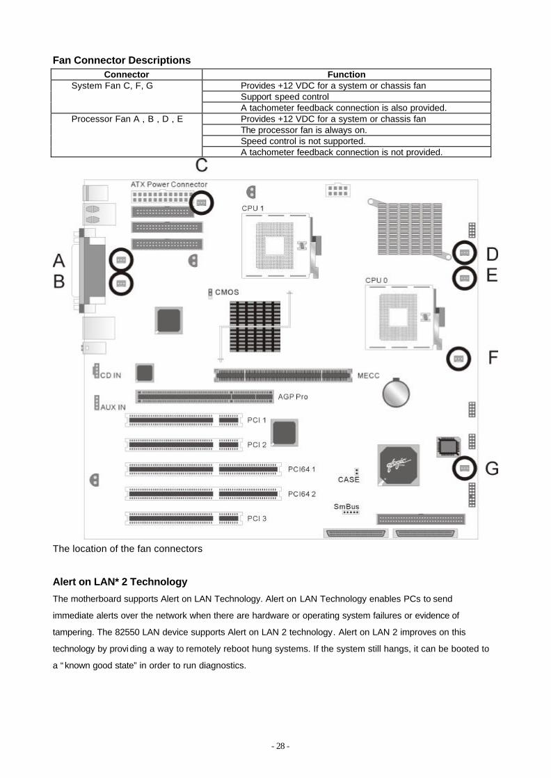
2 Motherboard Layout The picture shows the location of the major components on the motherboard.
A CPU 1 Fan Connector Q Internal Speaker B Primary IDE Connector R Qlogic 12160 SCSI Controller C Secondary IDE Connector S SCSI controller ROM D Diskette Drive Connector T Front 90x90mm System Fan Connector E WTX Power Connector A U Front Panel Connector F Rear 120x120mm Case Fan Connector V Ultra2 SCSI Connector G 82801BA I/O Controller Hub (ICH2) W Ultra-160 SCSI Connector B H Intel 82860 Memory Controller Hub (MCH) X Ultra-160 SCSI Connector A I CPU 1 Socket Y Rear Chassis Intrusion Detection J Memory Expansion Card Connector (MECC) Z 82802AB Firmware Hub (FWH) K WTX Power Connector B AA Intel 82806AA PCI 64 Hub (P64H) L DC-to-DC Converter AB PCI64 Slots M CPU 0 Fan Connector AC PCI Slots N CPU 0 Socket AD Aux_In Connector O Front 80x80mm System Fan Connector AE CD-ROM Connector P Battery AF Rear Panel Connectors
AG USB Internal Header AH IR Connector AI LAN 82550 Chipset AJ Temperature Sensor AK SCSI Activity LED Input
- 7 -
Supported Processors
This section describes the processors supported by the DX400-SN motherboard and how to install them.
The DX400-SN Motherboard only supports Intel Pentium Xeon processors with a Front
Side bus speed of 400 MHz . If two processors are installed, both processors must run the
same core frequency speed. Installing processors of different core frequencies speed may
damage the motherboard and processors.
The processor is packaged in a Organic Land Grid Array (OLGA). The Pentium Xeon Processors implement
integrated L2caches. The Pentium Xeon processor increases Performance for server and workstation
applications by adding either 512KB or 1MB of integrated L3 cache, which is also 8-way set associative.
The System Bus uses Source-Synchronous Transfer (SST) of address and data to improve performance and
enables data transfers at a frequency of 400MHz.This allows the processors to have 3.2GB/sec data transfer
rate .The control signals and bus phases are based on 100MHz system clock. This enhanced bus protocol
and internal architecture increases performance beyond previous levels.
The Processor Information ROM is a 128 byte read –only device that incorporates Intel processor specific
data .The OEM EEPROM, also known as the Scratchpad EEPROM, is a 128-byte read/write EEPROM in
which an OEM may program system specific data. The Thermal Sensor monitors the temperature of the
processor die.
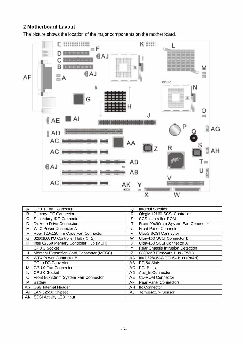
Installing the Processors and Retention Mechanism
Single processor:
Install the processor in the socket marked ‘CPU0’
For Dual processors
the following values must be identical for both processors:
· Host bus speed
· Processor core frequency
· Cache size
· Cache type (either discrete or advanced transfer)
· Operating voltages
Installing the retention on the motherboard.
- 8 -
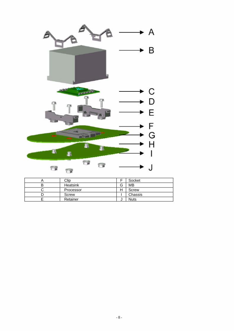
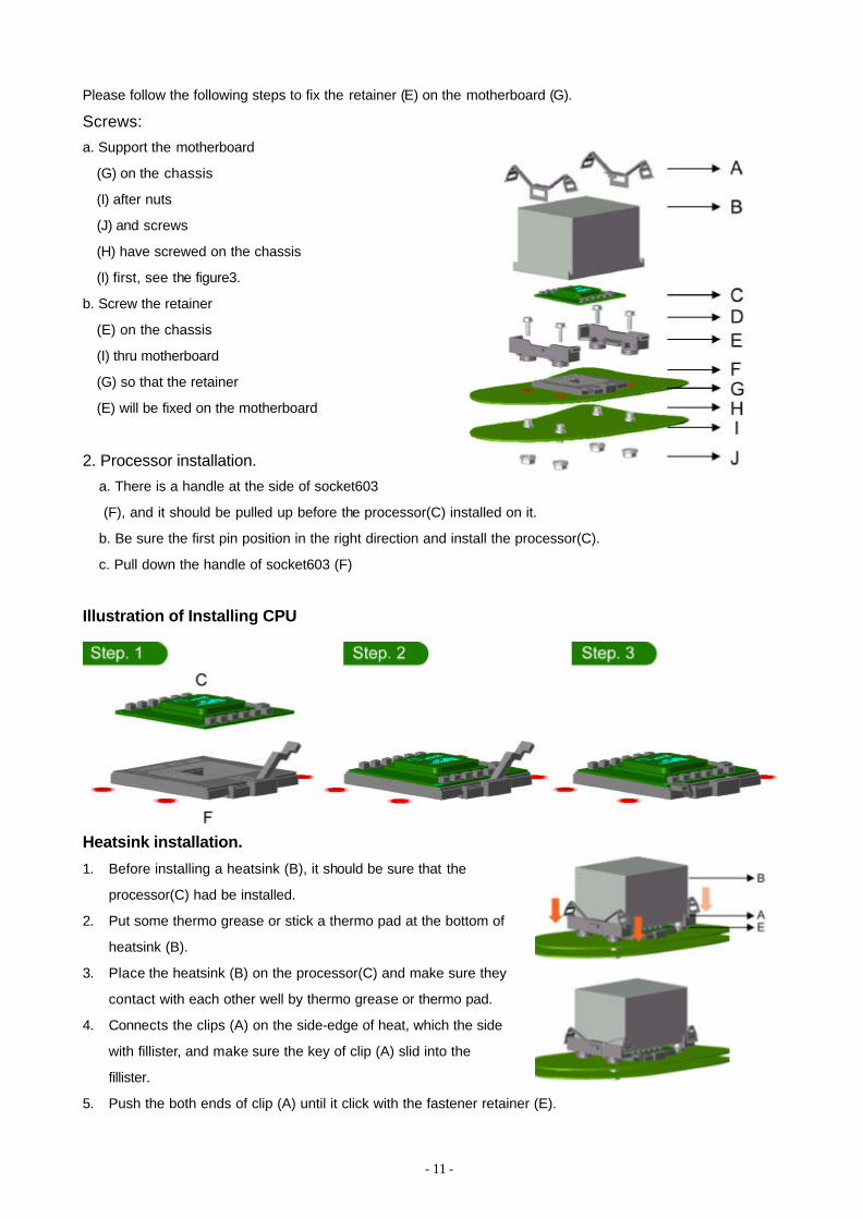
A Clip F Socket B Heatsink G MB C Processor H Screw D Screw I Chassis E Retainer J Nuts
- 9 -
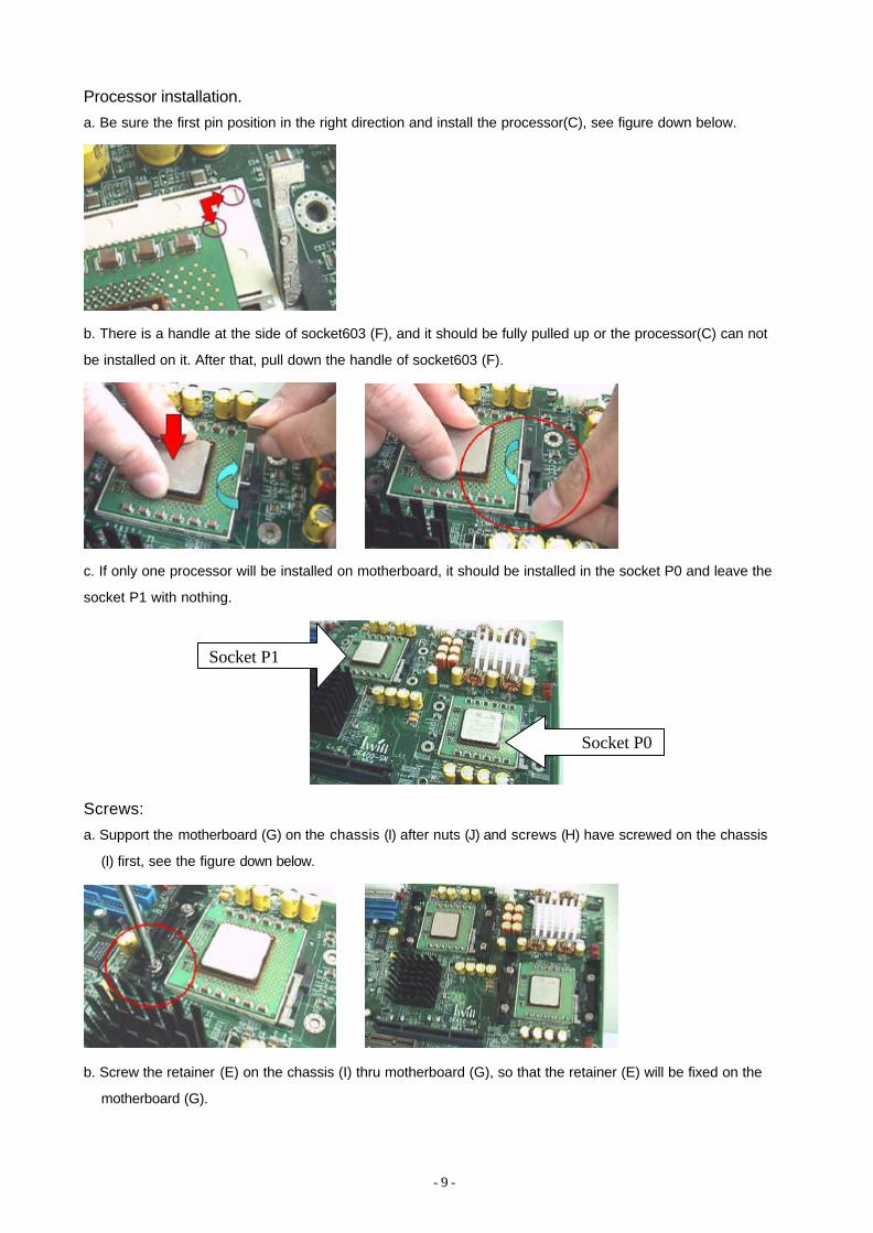
Processor installation.
a. Be sure the first pin position in the right direction and install the processor(C), see figure down below.
b. There is a handle at the side of socket603 (F), and it should be fully pulled up or the processor(C) can not
be installed on it. After that, pull down the handle of socket603 (F).
c. If only one processor will be installed on motherboard, it should be installed in the socket P0 and leave the
socket P1 with nothing.
Screws:
a. Support the motherboard (G) on the chassis (I) after nuts (J) and screws (H) have screwed on the chassis
(I) first, see the figure down below.
b. Screw the retainer (E) on the chassis (I) thru motherboard (G), so that the retainer (E) will be fixed on the
motherboard (G).
Socket P1
Socket P0
- 10 -
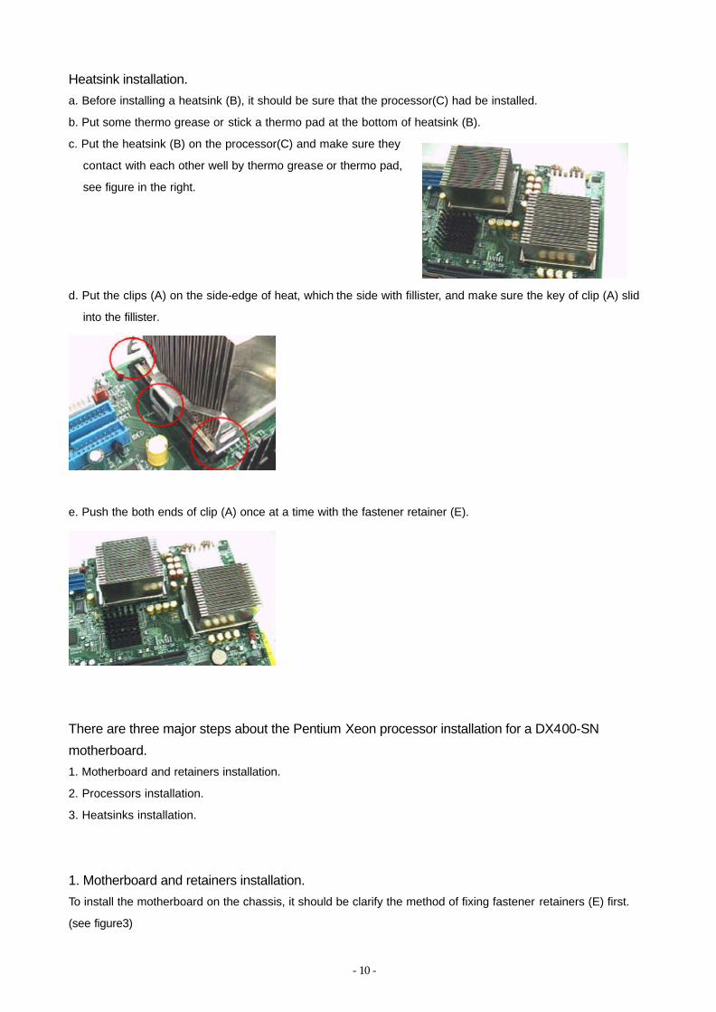
Heatsink installation.
a. Before installing a heatsink (B), it should be sure that the processor(C) had be installed.
b. Put some thermo grease or stick a thermo pad at the bottom of heatsink (B).
c. Put the heatsink (B) on the processor(C) and make sure they
contact with each other well by thermo grease or thermo pad,
see figure in the right.
d. Put the clips (A) on the side-edge of heat, which the side with fillister, and make sure the key of clip (A) slid
into the fillister.
e. Push the both ends of clip (A) once at a time with the fastener retainer (E).
There are three major steps about the Pentium Xeon processor installation for a DX400-SN
motherboard.
1. Motherboard and retainers installation.
2. Processors installation.
3. Heatsinks installation.
1. Motherboard and retainers installation.
To install the motherboard on the chassis, it should be clarify the method of fixing fastener retainers (E) first.
(see figure3)
- 11 -
Please follow the following steps to fix the retainer (E) on the motherboard (G).
Screws:
a. Support the motherboard
(G) on the chassis
(I) after nuts
(J) and screws
(H) have screwed on the chassis
(I) first, see the figure3.
b. Screw the retainer
(E) on the chassis
(I) thru motherboard
(G) so that the retainer
(E) will be fixed on the motherboard
2. Processor installation.
a. There is a handle at the side of socket603
(F), and it should be pulled up before the processor(C) installed on it.
b. Be sure the first pin position in the right direction and install the processor(C).
c. Pull down the handle of socket603 (F)
Illustration of Installing CPU
Heatsink installation.
1. Before installing a heatsink (B), it should be sure that the
processor(C) had be installed.
2. Put some thermo grease or stick a thermo pad at the bottom of
heatsink (B).
3. Place the heatsink (B) on the processor(C) and make sure they
contact with each other well by thermo grease or thermo pad.
4. Connects the clips (A) on the side-edge of heat, which the side
with fillister, and make sure the key of clip (A) slid into the
fillister.
5. Push the both ends of clip (A) until it click with the fastener retainer (E).

- 12 -
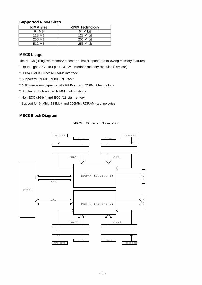
3.System Memory The Intel 82860 Memory Controller Hub (MCH) integrates dual Rambus* channels, providing a
processor to memory bandwidth up to 3.2 GB/sec.
MEC on motherboard
A Memory Expansion Card may be used to increase memory size configurations, which are required for
most server and workstation designs. The Intel 860 chipsets provide memory repeater hubs that allow for
this memory expandability. IWILL MEC card allows for memory support of up to 4GB.
ECC Memory
ECC memory detects multiple-bit errors and corrects single-bit errors. When ECC memory is installed, the
BIOS support both ECC and non-ECC modes. ECC mode is enabled in the Configuration Manager program.
The BIOS automatically detects if ECC memory is installed.
The Configuration Manager program provides an option for enabling and disabling ECC mode.
Whenever ECC mode is selected in Configuration Manager, a small performance difference may occur.
Memory Installation
The MEC8 contains TWO memory channels, in which a total of eight RIMMs banks. When using only four
RIMMs, you must install a Continuity Rambus Inline Memory Module (CRIMM) in those slots that do not
contain RIMMs.
You must first populate J8 and J4 and J7 and J3.
Below illustration show the correct method for installing RIMMs.
Here are the steps of memory installation.
a. Install the Rambus module on the slot of MEC8, see figure down below.
Notice where the key pin is, or it may not be installed.
- 13 -
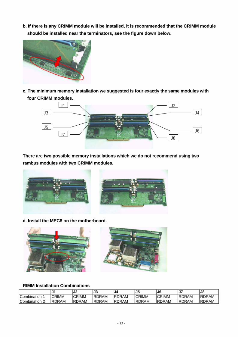
b. If there is any CRIMM module will be installed, it is recommended that the CRIMM module
should be installed near the terminators, see the figure down below.
c. The minimum memory installation we suggested is four exactly the same modules with
four CRIMM modules.
There are two possible memory installations which we do not recommend using two
rambus modules with two CRIMM modules.
d. Install the MEC8 on the motherboard.
RIMM Installation Combinations J1 J2 J3 J4 J5 J6 J7 J8 Combination 1 CRIMM CRIMM RDRAM RDRAM CRIMM CRIMM RDRAM RDRAM Combination 2 RDRAM RDRAM RDRAM RDRAM RDRAM RDRAM RDRAM RDRAM
J1 J3
J5 J7
J2 J4
J6 J8
- 14 -
Supported RIMM Sizes RIMM Size RIMM Technology
64 MB 64 M bit 128 MB 128 M bit 256 MB 256 M bit 512 MB 256 M bit
MEC8 Usage
The MEC8 (using two memory repeater hubs) supports the following memory features:
* Up to eight 2.5V, 184-pin RDRAM* interface memory modules (RIMMs*)
* 300/400MHz Direct RDRAM* interface
* Support for PC600 PC800 RDRAM*
* 4GB maximum capacity with RIMMs using 256Mbit technology
* Single- or double-sided RIMM configurations
* Non-ECC (16-bit) and ECC (18-bit) memory
* Support for 64Mbit ,128Mbit and 256Mbit RDRAM* technologies.
MEC8 Block Diagram
MRH-R (Device 1)
MRH-R (Device 2)
VTERM
VTERM
VTERM VTERM
VTERM VTERMCHA2 DGCG
MEC8 Block Diagram
MECC
EXA
EXB
CHA2 CHB2
CHB2 DGCG
CHA1 DGCG CHB1 DGCG
CHA1 CHB1
- 15 -
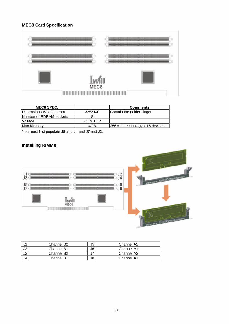
MEC8 Card Specification
MEC8 SPEC. Comments
Dimensions W x D in mm 325X140 Contain the golden finger Number of RDRAM sockets 8 Voltage 2.5 & 1.8V Max Memory 4GB 256Mbit technology x 16 devices
You must first populate J8 and J4.and J7 and J3.
Installing RIMMs
J1 Channel B2 J5 Channel A2 J2 Channel B1 J6 Channel A1 J3 Channel B2 J7 Channel A2 J4 Channel B1 J8 Channel A1

- 16 -
RIMM Installation Combinations J1 J2 J 3 J 4 J 5 J6 J 7 J 8
Combination 1 CRIMM CRIMM RDRAM RDRAM CRIMM CRIMM RDRAM RDRAM Combination 2 RDRAM RDRAM RDRAM RDRAM RDRAM RDRAM RDRAM RDRAM
CRIMMs must be installed in unpopulated RIMM connectors for the motherboard to boot. RIMMs
must be installed as described in above table or the motherboard will not boot. The memory
must be the same size, density, type, and speed.
Using the encoded part numbers on the RIMMs is the best way to determine if the parts are
the same.
- 17 -
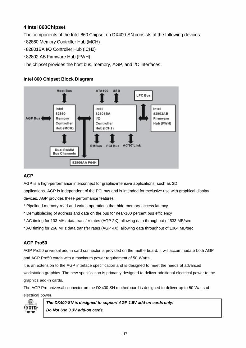
4 Intel 860Chipset The components of the Intel 860 Chipset on DX400-SN consists of the following devices:
· 82860 Memory Controller Hub (MCH)
· 82801BA I/O Controller Hub (ICH2)
· 82802 AB Firmware Hub (FWH).
The chipset provides the host bus, memory, AGP, and I/O interfaces.
Intel 860 Chipset Block Diagram
AGP
AGP is a high-performance interconnect for graphic-intensive applications, such as 3D
applications. AGP is independent of the PCI bus and is intended for exclusive use with graphical display
devices. AGP provides these performance features:
* Pipelined-memory read and writes operations that hide memory access latency
* Demultiplexing of address and data on the bus for near-100 percent bus efficiency
* AC timing for 133 MHz data transfer rates (AGP 2X), allowing data throughput of 533 MB/sec
* AC timing for 266 MHz data transfer rates (AGP 4X), allowing data throughput of 1064 MB/sec
AGP Pro50
AGP Pro50 universal add-in card connector is provided on the motherboard. It will accommodate both AGP
and AGP Pro50 cards with a maximum power requirement of 50 Watts.
It is an extension to the AGP interface specification and is designed to meet the needs of advanced
workstation graphics. The new specification is primarily designed to deliver additional electrical power to the
graphics add-in cards.
The AGP Pro universal connector on the DX400-SN motherboard is designed to deliver up to 50 Watts of
electrical power.
The DX400-SN is designed to support AGP 1.5V add-on cards only!
Do Not Use 3.3V add-on cards.
- 18 -
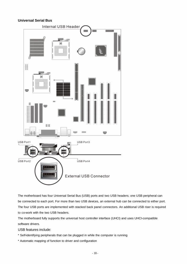
Universal Serial Bus
The motherboard has four Universal Serial Bus (USB) ports and two USB headers; one USB peripheral can
be connected to each port. For more than two USB devices, an external hub can be connected to either port.
The four USB ports are implemented with stacked back panel connectors. An additional USB riser is required
to co-work with the two USB headers.
The motherboard fully supports the universal host controller interface (UHCI) and uses UHCI-compatible
software drivers.
USB features include:
* Self-identifying peripherals that can be plugged in while the computer is running
* Automatic mapping of function to driver and configuration

- 19 -
* Support for isochroous and asynchronous transfer types over the same set of wires
* Support for up to 127 physical devices
* Guaranteed bandwidth and low latencies appropriate for telephony, audio and other applications
* Error-handling and fault-recovery mechanisms built into the protocol
The USB controller provides enhanced support for the Universal Host Controller Interface (UHCI). This includes support that allows
legacy software to use a USB-based keyboard and mouse. The ICH2 is USB Revision 1.1 compliant. The ICH2 contains two USB Host
Controllers. Each Host Controller includes a root hub with two separate USB ports each, for a total of 4 USB ports.
IDE Support
The motherboard has two independent bus-mastering IDE interfaces. These interfaces support:
* ATAPI devices (such as CD-ROM drives)
*ATA devices using the single-word DMA 0, 1, and 2 and multiword DMA 1 and 2, PIO 0-4

- 20 -
The BIOS supports logical block addressing (LBA) and extended cylinder head sector (ECHS)
translation modes. The drive reports the transfer rate and translation mode to the BIOS.
The motherboard supports laser servo (LS-120) diskette technology through its IDE interfaces.
The LS-120 drive can be configured as a boot drive.
The motherboard allows connection of an LS-120 compatible drive and a standard 3.5-inch diskette drive..
The ICH2 supports the IDE controller with two sets of interface signals (Primary and Secondary). It supports
the Ultra ATA/33, Ultra ATA/66 and Ultra ATA/100 protocols. Ultra ATA66 and Ultra ATA/100 are similar to the
Ultra ATA/33 scheme and are intended to be device driver compatible. The Ultra ATA/66 logic clocks at 66
MHz and can move 16bit of data every two clocks, and the Ultra ATA/100 logic clocks at 100MHz can move
16-bit of data every two clock (for a maximum of 100 MB/s)
Real-Time Clock, CMOS SRAM, and Battery
The real-time clock is compatible with DS1287 and MC146818 components. This device provides a
time-of-day clock and a multi-century calendar with alarm features and century rollover. The real-time clock
supports 256 bytes of battery-backed CMOS RAM in two banks that are reserved for BIOS use.
The time, date, and CMOS values can be specified in the Bios Setup. The CMOS values can be returned to
their defaults by using the Bios Setup. An external coin-cell battery powers the real-time clock and CMOS
memory. When the computer is not plugged into a wall socket, the battery has an estimated life of three
years. When the computer is plugged in, the standby current from the power supply extends the life of the
battery.
The clock is accurate to +/-13 minutes/year at 25ºC with 3 VSB applied.
- 21 -
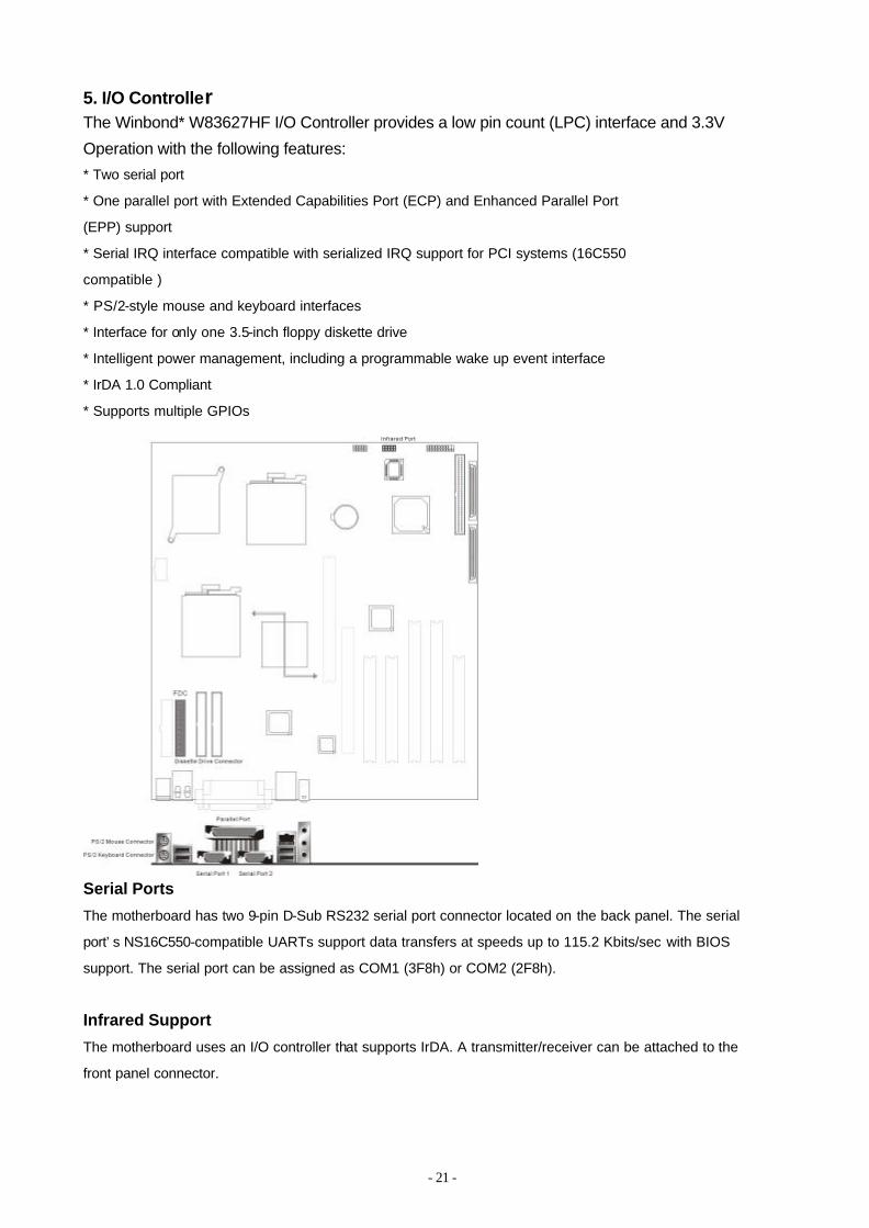
5. I/O Controller The Winbond* W83627HF I/O Controller provides a low pin count (LPC) interface and 3.3V
Operation with the following features:
* Two serial port
* One parallel port with Extended Capabilities Port (ECP) and Enhanced Parallel Port
(EPP) support
* Serial IRQ interface compatible with serialized IRQ support for PCI systems (16C550
compatible )
* PS/2-style mouse and keyboard interfaces
* Interface for only one 3.5-inch floppy diskette drive
* Intelligent power management, including a programmable wake up event interface
* IrDA 1.0 Compliant
* Supports multiple GPIOs
Serial Ports
The motherboard has two 9-pin D-Sub RS232 serial port connector located on the back panel. The serial
port’s NS16C550-compatible UARTs support data transfers at speeds up to 115.2 Kbits/sec with BIOS
support. The serial port can be assigned as COM1 (3F8h) or COM2 (2F8h).
Infrared Support
The motherboard uses an I/O controller that supports IrDA. A transmitter/receiver can be attached to the
front panel connector.

- 22 -
Parallel Port
The connector for the multi-mode, bi-directional parallel port is a 25-pin D-sub connector located on the back
panel. In the BIOS Configuration Manager program, the parallel port can be configured for the following:
* Output only (PC AT*-compatible mode)
* Bi-directional (PS/2 compatible)
* Extended Parallel Port (EPP)
* Enhanced Capabilities Port (ECP)
Diskette Drive Controller
The diskette drive controller is software compatible with the DP8473 and N82077 diskette drive controllers
and supports both PC-AT* and PS/2* modes. In the Configuration Manager program, the diskette drive
interface can be configured to support one 3.5-inch diskette drives for the following capacities and sizes:
* 1.44 MB, 3.5-inch
Keyboard and Mouse Interface
PS/2 keyboard and mouse connectors are located on the back panel. The +5V lines to these
connectors are protected with a Poly Switch * circuit that, like a self-healing fuse, reestablishes the
connection after an over-current condition is removed.
The keyboard controller provides the keyboard and mouse control functions. A power on/reset
password can be specified in the Configuration Manager.
The keyboard controller also supports the hot-key sequence <Ctrl><Alt><Del> for a software reset.
This key sequence resets the computer’s software by jumping to the beginning of the BIOS code and running
the Power-on Self Test (POST).
- 23 -
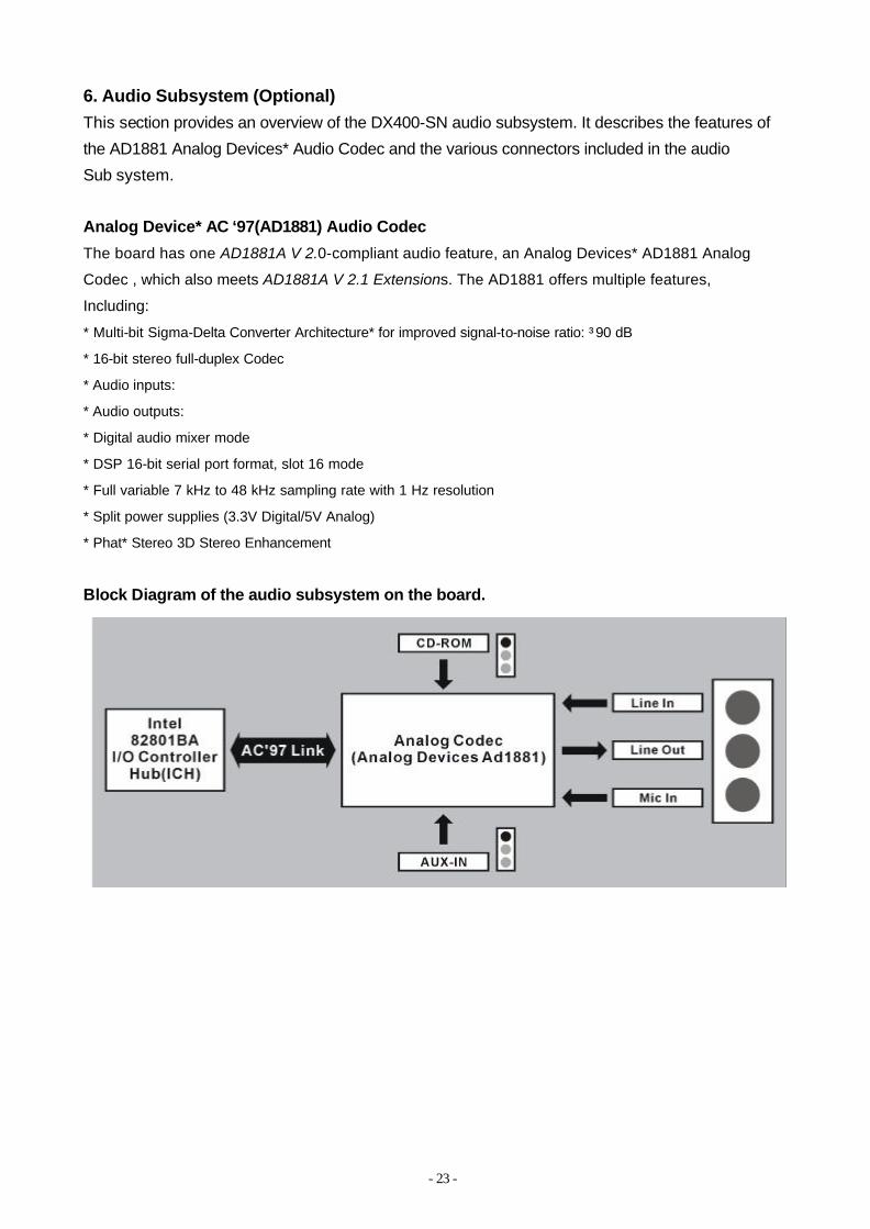
6. Audio Subsystem (Optional) This section provides an overview of the DX400-SN audio subsystem. It describes the features of
the AD1881 Analog Devices* Audio Codec and the various connectors included in the audio
Sub system.
Analog Device* AC ‘97(AD1881) Audio Codec
The board has one AD1881A V 2.0-compliant audio feature, an Analog Devices* AD1881 Analog
Codec , which also meets AD1881A V 2.1 Extensions. The AD1881 offers multiple features,
Including:
* Multi-bit Sigma-Delta Converter Architecture* for improved signal-to-noise ratio: ³90 dB
* 16-bit stereo full-duplex Codec
* Audio inputs:
* Audio outputs:
* Digital audio mixer mode
* DSP 16-bit serial port format, slot 16 mode
* Full variable 7 kHz to 48 kHz sampling rate with 1 Hz resolution
* Split power supplies (3.3V Digital/5V Analog)
* Phat* Stereo 3D Stereo Enhancement
Block Diagram of the audio subsystem on the board.
- 24 -
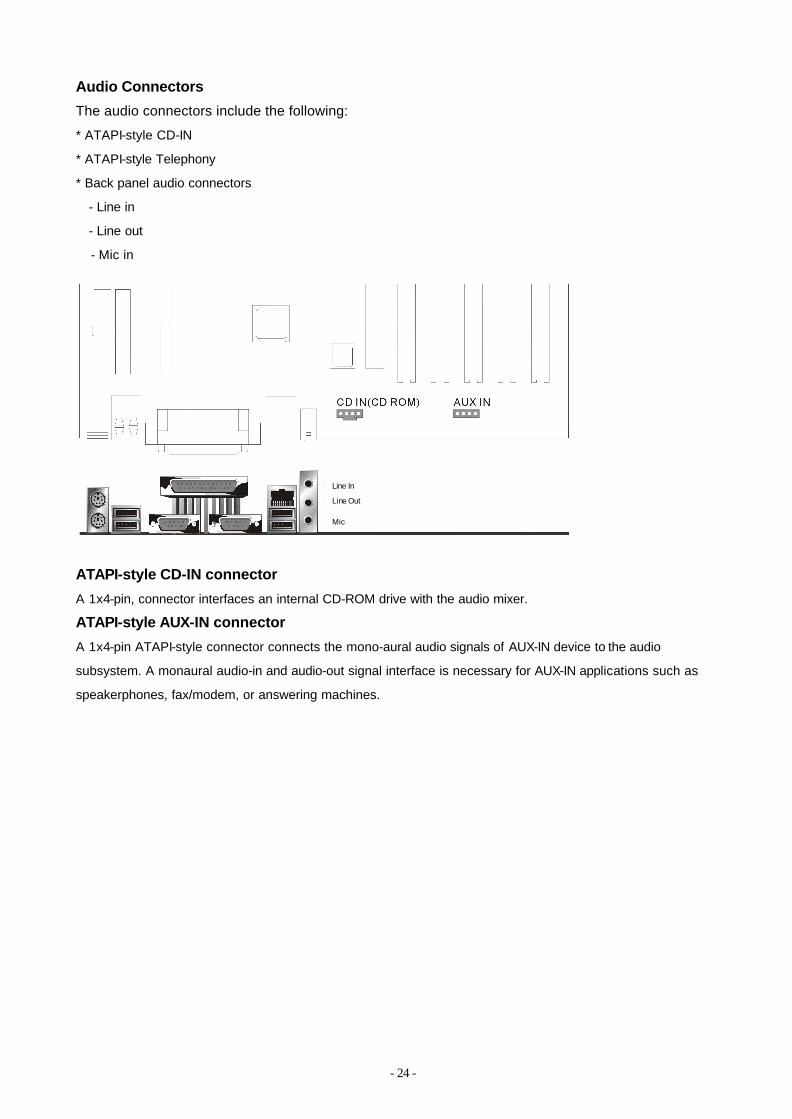
Audio Connectors
The audio connectors include the following:
* ATAPI-style CD-IN
* ATAPI-style Telephony
* Back panel audio connectors
- Line in
- Line out
- Mic in
ATAPI-style CD-IN connector
A 1x4-pin, connector interfaces an internal CD-ROM drive with the audio mixer.
ATAPI-style AUX-IN connector
A 1x4-pin ATAPI-style connector connects the mono-aural audio signals of AUX-IN device to the audio
subsystem. A monaural audio-in and audio-out signal interface is necessary for AUX-IN applications such as
speakerphones, fax/modem, or answering machines.
Line In
Line Out
Mic

- 25 -
7. Hardware Management Features The hardware management features enable the board to be compatible with the Wired for
Management ( WfM ) specification. The board has several hardware management features,
Including the following:
* Hardware monitor subsystem
* Chassis intrusion detection connectors
* Fan control and monitoring Hardware Monitor Subsystem
The hardware monitor subsystem provides low-cost instrumentation capabilities. The features of
the hardware monitor subsystem include:
* Management Level 5 functionality
* Microprocessor System Hardware Monitor ( Winbond W83627HF)
- Integrated temperature and voltage monitoring to detect levels above or below
acceptable values (1.8V, 3.3 V, 5 V, 12 V). When programmed ratings for
temperatures or voltages are exceeded, an interrupt is activated.
- Access through the SMBus
* Internal ambient temperature sensing through an on-board thermistor
* Remote reset capabilities from a remote peer or server through Intel LANDesk (or
later) Client Manager 6.0 (LDCM) and service layers
*chassis intrusion connector.
Chassis Intrusion Detection Connectors
The hardware monitor subsystem supports a chassis security feature that detects if the chassis cover is
removed. When the chassis cover is removed, a signal is sent to the hardware monitor component. The
chassis intrusion circuit is powered by either the chassis’ power supply (when the computer is connected to
AC power) or the battery (when the computer is not connected to AC power).
The security feature uses mechanical switches on the chassis that are attached to the chassis
intrusion detect connectors. The switch contacts are open for normal computer operation. As a
result , a normally open switch should be used for chassis intrusion. When the chassis cover is
removed, the switch contacts close, and the circuit to ground is completed.
Fan Control and Monitoring
The motherboard includes eight fan power connectors: four connectors for fans on the processor heat sinks,
and four connectors for speed-controlled system fans. All eight connectors are 3-pin headers. Only system
fan support fan tachometer monitoring. The processor heat sink fans are not speed controlled.
The system fans use the motherboard fan speed control, which consists of three states: off, normal speed,
and high speed. In normal operation, the system fans operate at normal speed until the thermal sensor
junction temperature reaches the high-speed fan threshold temperature. The system fans operate at high
speed when the temperature threshold is exceeded.

- 26 -
This threshold temperature can be set in the Configuration Manager.
The user can set the threshold to 40°C for continuous operation of the system fans in high-speed
mode in the S0 and S1 sleep states.
Controlling System Fan Speed
1. Set the Auto Fan Startup Temperature as minimum degree.
2. Adjust the Range as the working range of fans.
3. The fans will be changed to automatic speed between the minimum and maximum temperature as we set.
The left picture is captured from ADM1031 evaluation software during testing.
A. “Temperature vs. Time” shows the temperature detected from a thermo sensor.
B. “RPM vs. Time” represents the Fans speed from the fan
controlled by “ADM1031” software.
Therefore, the initial condition assumed to be as follow:
The Auto Fan Startup Temp = 40°C (startup temperature)
The Auto Fan Startup Range = 20°C (T range)
The maximum rotating speed of fan is 2500 RPM.
How does it work?
Point A: The “green A “indicates the fan start to rotate at startup temperature.
Point B: The “green B” indicates a maximum temperature 60*C which come from Startup Temp plus T range. It means T
max 60*C = 40*C + 20*C.
Between Point A and Point B:
When the sensor detects a temperature between “green A “and “green B”, the fan will be adjusted in rotating speed. It
means that “ Fan Min Speed< fan speed < Fan Max Speed ” when “ 40*C < temperature < 60*C”.
There is a filter function set in default to make the fan acting not that sensitive to the temperature. Filter mode is for two
reason, one is longer the fan’s life, the other is lower the noise. As you can see, at the “green B”, the fan speed did not
reach its maximum when the temperature exceeded the T max. In another word, filter mode makes the fan more
insensitive to the temperature.
Region E: The “red E” indicates the fan speed will keep rotating in maximum speed when temperature is beyond T max.
Between Point C and Point D: From “green C” down to 40*C, it is the same function that the fan speed will be adjusted
depending on the temperature degree. Normally, once the fan had been activated, it will not stop until the temperature
down to 35*C.
35*C = Startup Temp 40*C – 5*C
The value 35*C is only for this initial condition.
For example, in another case, the fan will stop rotating at 23*C when the Startup Temp is set to 28*C.
The green D indicates the fan stop rotating when the temperature down to 35*C.
- 27 -
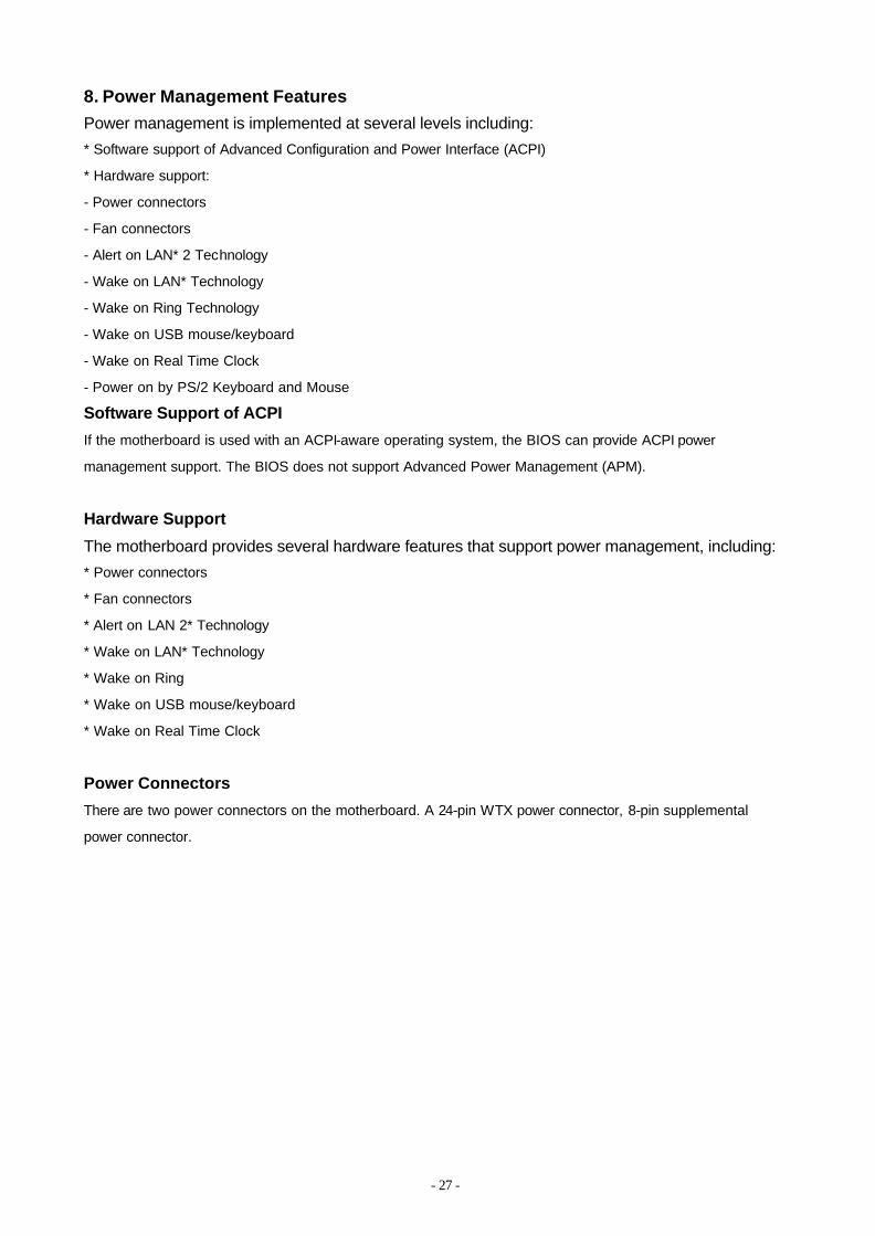
8. Power Management Features Power management is implemented at several levels including:
* Software support of Advanced Configuration and Power Interface (ACPI)
* Hardware support:
- Power connectors
- Fan connectors
- Alert on LAN* 2 Technology
- Wake on LAN* Technology
- Wake on Ring Technology
- Wake on USB mouse/keyboard
- Wake on Real Time Clock
- Power on by PS/2 Keyboard and Mouse
Software Support of ACPI
If the motherboard is used with an ACPI-aware operating system, the BIOS can provide ACPI power
management support. The BIOS does not support Advanced Power Management (APM).
Hardware Support
The motherboard provides several hardware features that support power management, including:
* Power connectors
* Fan connectors
* Alert on LAN 2* Technology
* Wake on LAN* Technology
* Wake on Ring
* Wake on USB mouse/keyboard
* Wake on Real Time Clock
Power Connectors
There are two power connectors on the motherboard. A 24-pin WTX power connector, 8-pin supplemental
power connector.
- 28 -
Fan Connector Descriptions Connector Function
Provides +12 VDC for a system or chassis fan Support speed control
System Fan C, F, G
A tachometer feedback connection is also provided. Provides +12 VDC for a system or chassis fan The processor fan is always on. Speed control is not supported.
Processor Fan A , B , D , E
A tachometer feedback connection is not provided.
The location of the fan connectors
Alert on LAN* 2 Technology
The motherboard supports Alert on LAN Technology. Alert on LAN Technology enables PCs to send
immediate alerts over the network when there are hardware or operating system failures or evidence of
tampering. The 82550 LAN device supports Alert on LAN 2 technology. Alert on LAN 2 improves on this
technology by provi ding a way to remotely reboot hung systems. If the system still hangs, it can be booted to
a “known good state” in order to run diagnostics.
- 29 -
Wake on LAN Technology
Wake on LAN Technology enables remote wakeup of the computer through a network. The LAN subsystem
monitors network traffic at the Media Independent Interface. Upon detecting a Magic Packet * frame, the LAN
subsystem asserts a wakeup signal that powers up the computer. The motherboard supports Wake on LAN
through the PCI bus PME# signal and the Intel 82550 LAN controller. This signal can wake up the computer
only when the power cord is still plugged into the socket and the computer is in a supported sleep state.
Wake on LAN can be enabled or disabled through the BIOS Configuration Manager program. A Wake on
LAN connector is not required.
Wake on LAN* Technology requires power from the +5V standby line. If the Wake on LAN
technology feature is used, ensure that the power supply provides adequate +5V standby
current (1.0A). Failure to do so can damage the power supply.
For Wake on LAN technology, the 5V standby line for the power supply must be capable of
providing adequate +5V standby current (1.0A). Failure to provide adequate standby current
when implementing Wake on LAN Technology can damage the power supply.
Wake on Ring Technology
Wake on Ring allows the computer to be awakened from the supported ACPI sleep states. It requires two
calls to access the computer: the first call wakeup the computer, the second call enables access. Wake on
Ring enables the computer to detect incoming calls differently for external as opposed to internal modems.
Wake on Ring enables telephony devices to access the computer when it is in a
power-managed state. The method used depends on the type of telephony device (external
or internal) and the power management mode being used.
Wake on USB
Wake on USB allows the computer to be awakened from supported ACPI sleep states. When the system
receives input from a USB mouse or keyboard, it wakes from the supported ACPI sleep state that it is in.
Wake on USB allows the motherboard to be awakened by inputs from a USB mouse or USB
keyboard. The motherboard can also be awakened from Real Time Clock alerts
- 30 -
9 LAN Subsystem (optional) The Intel 82550 10/100 Mbps Fast Ethernet, Wired for Management (WfM) support, LAN subsystem
provides both 10Base-T and 100Base-TX connectivity. Features include
* Full Duplex support at both10Base-T and 100Base-TX capability using a single RJ-45 connector
* 32-bit, 33MHz direct bus mastering on the PCI bus
* IEEE 802.3u Auto-Negotiation support
Intel 82550 LAN Controller (optional)
The Intel 82550 10/100 Mbps Faster Ethernet LAN controller’s features include:
* CSMA/CD Protocol Engine
* 32-bit PCI bus interface
* DMA engine for movement of commands, status, and network data across the PCI bus
* Integrated physical layer interface, including:
- Complete support for the 10Base-T and 100Base-TX network interfaces; when in 10Mbit/sec mode, the interface drives
the cable directly
- 802.3u Auto-Negotiation for automatically establishing the best operating mode when connected to other 10Base-T or
100Base-TX devices, whether half- or full-duplex capable
* Integrated power management features, including:
-System Management Bus support
-Support for ACPI technology
-Support for Wake on LAN and Alert on LAN 2 technology
* High Performance Networking Functions features, including:
- Improved dynamic transmit chaining with multiple priorities transmit queues
Fast back-to-back transmission support with minimum inter frame spacing
Alert On LAN Component (optional)
The Alert on LAN component is a companion device to the Intel 82550 LAN controller. Together, these
devices provide a management interface between a remote management console (or management server)
and a client system monitoring instrumentation. When an alert input is asserted, the Alert on LAN component
transmits Ethernet packets to the 82550 through an 8-bit dedicated data path. Examples of events that can
trigger alert messages to a management server include:
* Chassis intrusion
* System BIOS hang (transmits POST error code)
* LAN leash (transmits an alert that the LAN cable was disconnected)
* Temperature or voltage out of specification
LAN Subsystem Software
The Intel 82550 10/100 Mbps Fast Ethernet WfM PCI LAN software and drivers are available from Intel’s
World Wide Web site

- 31 -
RJ-45 LAN Connector (Optional) LEDs
Two LEDs are built into the RJ-45 LAN connector. The table describes the LED states when the board is
powered up and the LAN subsystem is operating.
LAN Connector LED States LED Color LED State Condition
Green Off 10 M bit/sec The speed is selected On 100 M bit/sec The speed is selected Yellow Off LAN link is not established
On (steady state) LAN link is not established On (brighter and pulsing) Traffic On the LAN
- 32 -
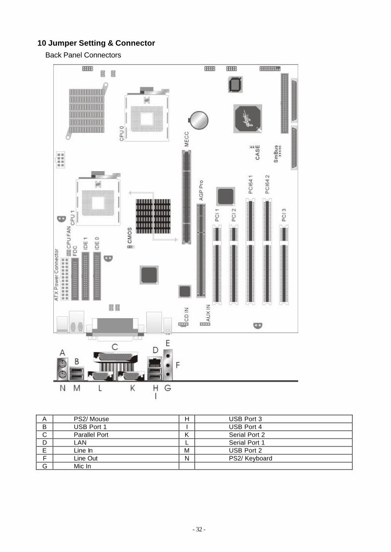
10 Jumper Setting & Connector Back Panel Connectors
A PS2/ Mouse H USB Port 3 B USB Port 1 I USB Port 4 C Parallel Port K Serial Port 2 D LAN L Serial Port 1 E Line In M USB Port 2 F Line Out N PS2/ Keyboard G Mic In
- 33 -
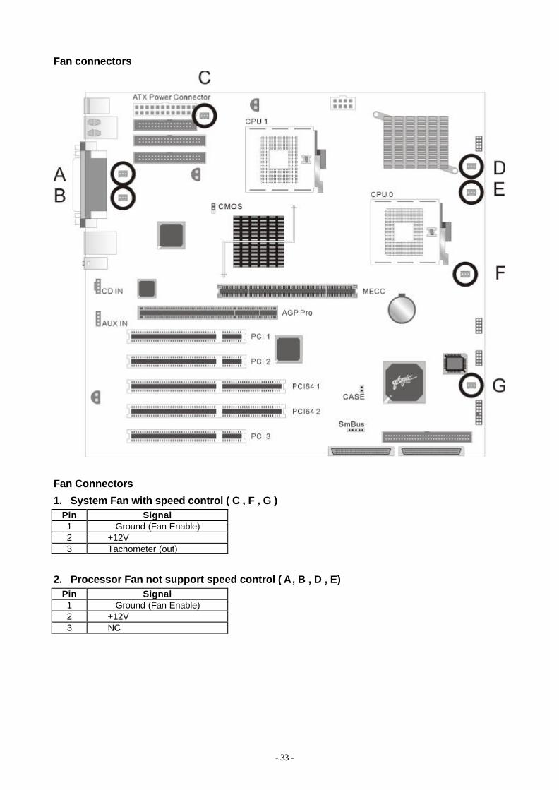
Fan connectors
Fan Connectors
1. System Fan with speed control ( C , F , G ) Pin Signal 1 Ground (Fan Enable) 2 +12V 3 Tachometer (out)
2. Processor Fan not support speed control ( A , B , D , E) Pin Signal 1 Ground (Fan Enable) 2 +12V 3 NC
- 34 -
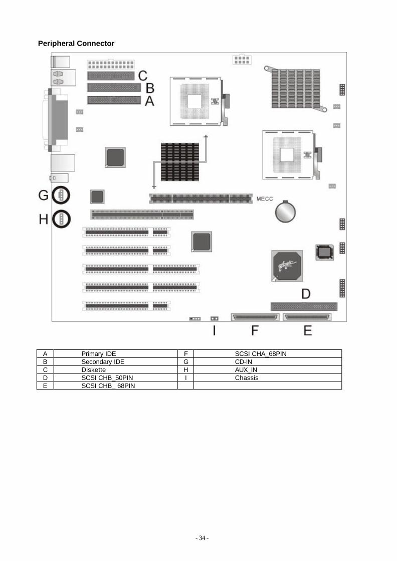
Peripheral Connector
A Primary IDE F SCSI CHA_68PIN B Secondary IDE G CD-IN C Diskette H AUX_IN D SCSI CHB_50PIN I Chassis E SCSI CHB_ 68PIN
- 35 -
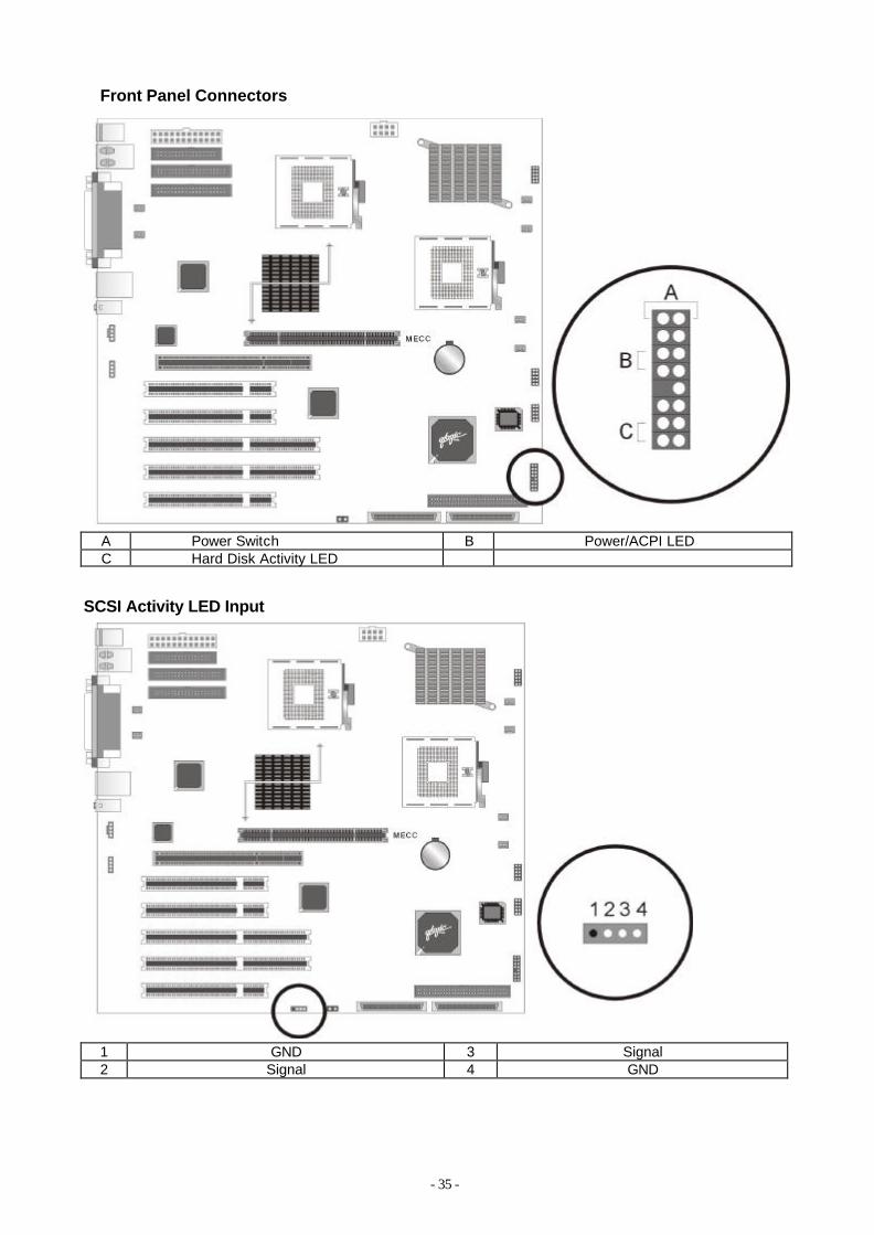
Front Panel Connectors
A Power Switch B Power/ACPI LED C Hard Disk Activity LED
SCSI Activity LED Input
1 GND 3 Signal 2 Signal 4 GND
- 36 -
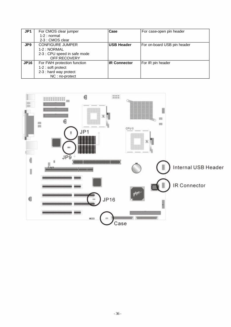
JP1 For CMOS clear jumper
1-2 : normal 2-3 : CMOS clear
Case For case-open pin header
JP9 CONFIGURE JUMPER 1-2 : NORMAL 2-3 : CPU speed in safe mode
OFF:RECOVERY
USB Header For on-board USB pin header
JP16 For FWH protection function 1-2 : soft protect 2-3 : hard way protect
NC : no-protect
IR Connector For IR pin header
- 37 -
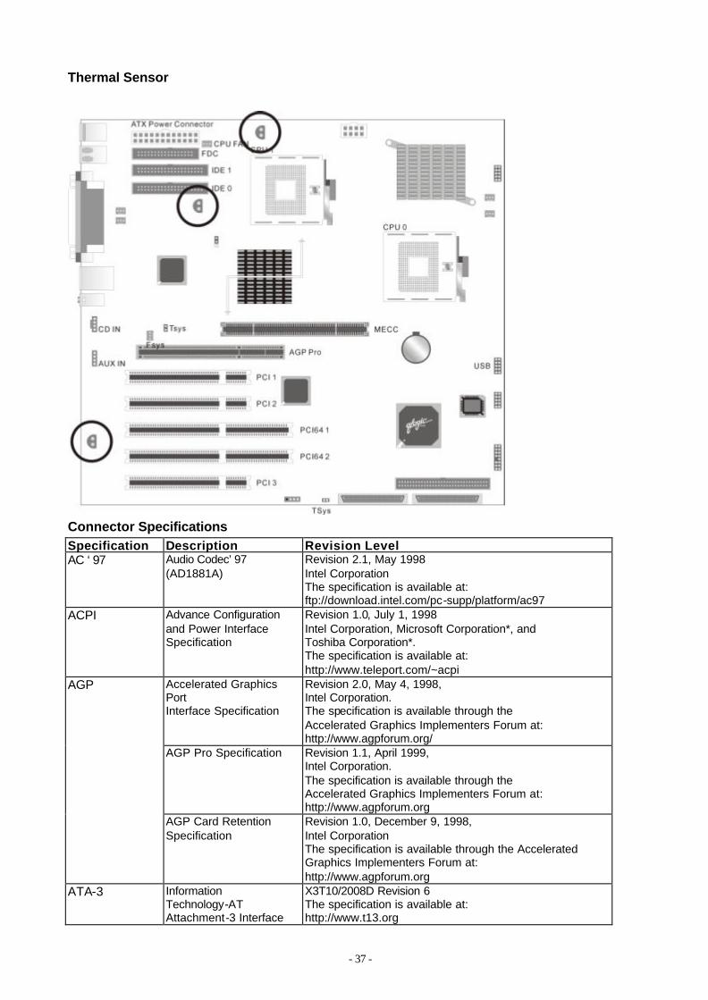
Thermal Sensor
Connector Specifications Specification Description Revision Level AC ‘97 Audio Codec’97
(AD1881A) Revision 2.1, May 1998 Intel Corporation The specification is available at: ftp://download.intel.com/pc-supp/platform/ac97
ACPI Advance Configuration and Power Interface Specification
Revision 1.0, July 1, 1998 Intel Corporation, Microsoft Corporation*, and Toshiba Corporation*. The specification is available at: http://www.teleport.com/~acpi
Accelerated Graphics Port Interface Specification
Revision 2.0, May 4, 1998, Intel Corporation. The specification is available through the Accelerated Graphics Implementers Forum at: http://www.agpforum.org/
AGP Pro Specification Revision 1.1, April 1999, Intel Corporation. The specification is available through the Accelerated Graphics Implementers Forum at: http://www.agpforum.org
AGP
AGP Card Retention Specification
Revision 1.0, December 9, 1998, Intel Corporation The specification is available through the Accelerated Graphics Implementers Forum at: http://www.agpforum.org
ATA-3 Information Technology-AT Attachment-3 Interface
X3T10/2008D Revision 6 The specification is available at: http://www.t13.org
- 38 -
ATAPI ATA Packet Interface for CD-ROMS
X3T10/2008D Revision 6 The specification is available at: http://www.t13.org
ATX ATX Specification Revision 2.01, February 1997 Intel Corporation The specification is available at: http://developer.intel.com/design/motherbd/atx.htm
EPP Enhanced Parallel Port IEEE 1284.1 standard, Mode [1 or 2], v1.7 IEEE The specification is available at: http://standards.ieee.org/
El Torito Bootable CD-ROM format specification
Version 1.0, January 25, 1995 Phoenix Technologies Ltd., and IBM Corporation The specification is available on the Phoenix Website at: http://www.ptltd.com/products/specs.htm
LPC Low Pin Count Interface Specification
Revision 1.0, September 29, 1997 Intel Corporation This specification is available at: http://www.intel.com/design/chipsets/industry/lpc.htm
MTBF Bellcore Reliability Prediction Procedure
BTR-NWT-000332, Issue 4, September 1991.
Multiprocessor System
Multiprocessor specification
Version 1.4, May 1997 Intel Corporation This specification is available at: http://developer.intel.com/design/intarch/manuals
PCI Local Bus Specification
Revision 2.2, December 18, 1998, PCI Special Interest Group This specification is available at: http://www.pcisig.com/
PCI
PCI Bus Power Management Interface Specification
Revision 1.1, December 18, 1998, PCI Special Interest Group. The specification is available at: http://www.pcisig.com/
Power Supply Intel 300W Power Supply Design Guide
Revision 1.0, June 1998 Intel Corporation. The specification is available at: http://www.intel.com/
PS/2* PS/2 Port Specification September 1991 IBM Corporation*
PXE Boot ROM Preboot Execution Environment Specification
Version 2.0 Intel Corporation The specification is available at: http://developer.intel.com/ial/wfm/wfmspecs.htm
RIMM Rambus Serial Presence Detect (SPD) Specification
Revision 1.0, March 1999 Rambus Corp.* The specification is available at: http://www.rimm.com http://www.rambus.com
SMBIOS System Management BIOS
Version 2.3, 12 August 1998, Award Software International Inc.*, Dell Computer Corporation*, Hewlett-Packard Company*, Intel Corporation, International Business Machines Corporation*, Phoenix Technologies Limited*, American Megatrends Inc.*, and SystemSoft Corporation* The specification is available at: http://developer.intel.com/ial/wfm/design/smbios
UHCI Universal Host Controller Interface
Design Guide Revision 1.1, March 1996, Intel Corporation The guide is available at: http://www.usb.org/developers
USB Universal Serial Bus Specification
Revision 1.1, September 23, 1998, Compaq Computer Corporation*, Digital Equipment
- 39 -
Corporation*, IBM Corporation*, Intel Corporation, Microsoft Corporation*, NEC*, and Northern Telecom* The specification is available at: http://www.usb.org/developers
WfM Wired for Management Baseline
Version 2.0, December 18, 1998, Intel Corporation The specification is available at: http://developer.intel.com/ial/WfM/wfmspecs.htm
WTX Workstation Chassis Specification
Version 1.1, February 1999 Intel Corporation The specification is available at: http://www.wtx.org
PS/2 Keyboard/Mouse Connectors Pin Signal Name 1 Data 2 Not connected 3 Ground 4 Fused +5 V 5 Clock 6 Not connected
Serial Port Connector Pin Signal Name Pin Signal Name 1 DCD 6 DSR# 6 DSR# 2 Serial In# 7 RTS# 7 RTS# 3 Serial Out# 8 CTS# 8 CTS# 4 DTR# 9 RI# 9 RI# 5 Ground
Parallel Port Connector Pin Signal Name Pin Signal Name 1 Strobe# 2 Auto Feed# 3 Data bit 0 4 Fault# 5 Data bit 1 6 INIT# 7 Data bit 2 8 SLCT IN# 9 Data bit 3 10 Ground 11 Data bit 4 12 Ground 13 Data bit 5 14 Ground 15 Data bit 6 16 Ground 17 Data bit 7 18 Ground 19 ACK# 20 Ground 21 Busy 22 Ground 23 Error 24 Ground 25 Select
Line In Connector Pin Signal Name
Sleeve Ground Tip Audio Left In
Ring Audio Right In
- 40 -
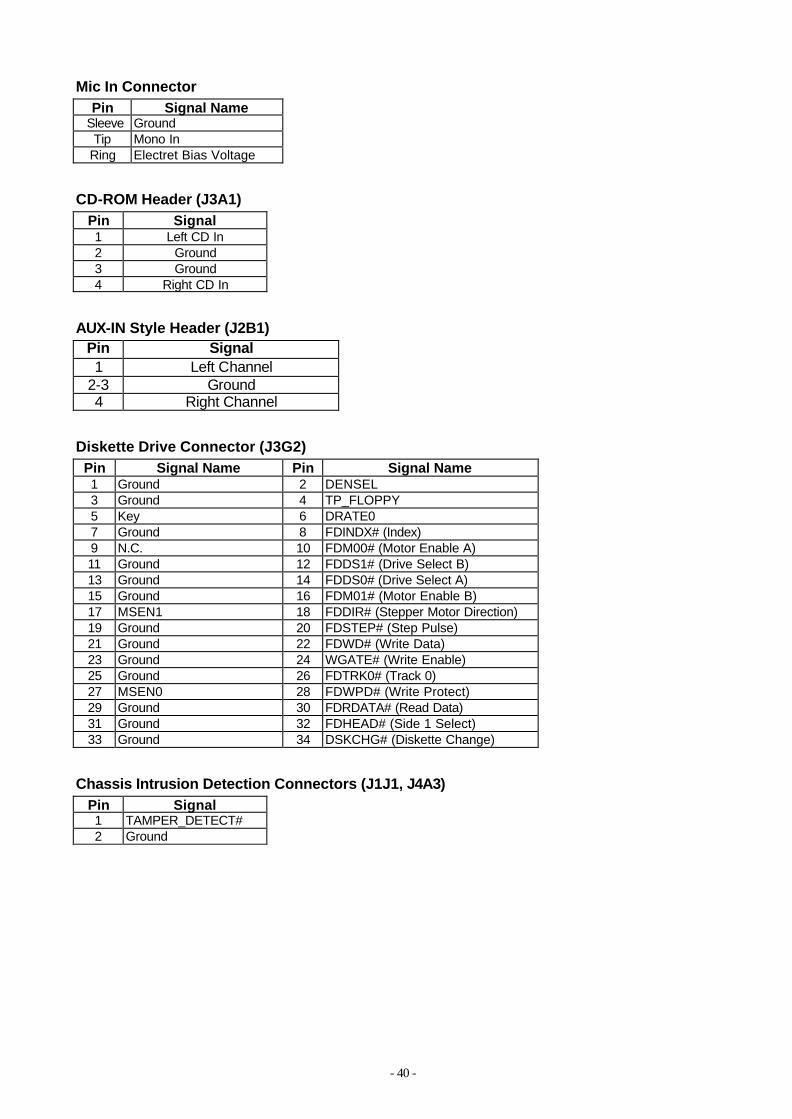
Mic In Connector Pin Signal Name
Sleeve Ground Tip Mono In
Ring Electret Bias Voltage
CD-ROM Header (J3A1) Pin Signal 1 Left CD In 2 Ground 3 Ground 4 Right CD In
AUX-IN Style Header (J2B1) Pin Signal 1 Left Channel
2-3 Ground 4 Right Channel
Diskette Drive Connector (J3G2) Pin Signal Name Pin Signal Name 1 Ground 2 DENSEL 3 Ground 4 TP_FLOPPY 5 Key 6 DRATE0 7 Ground 8 FDINDX# (Index) 9 N.C. 10 FDM00# (Motor Enable A) 11 Ground 12 FDDS1# (Drive Select B) 13 Ground 14 FDDS0# (Drive Select A) 15 Ground 16 FDM01# (Motor Enable B) 17 MSEN1 18 FDDIR# (Stepper Motor Direction) 19 Ground 20 FDSTEP# (Step Pulse) 21 Ground 22 FDWD# (Write Data) 23 Ground 24 WGATE# (Write Enable) 25 Ground 26 FDTRK0# (Track 0) 27 MSEN0 28 FDWPD# (Write Protect) 29 Ground 30 FDRDATA# (Read Data) 31 Ground 32 FDHEAD# (Side 1 Select) 33 Ground 34 DSKCHG# (Diskette Change)
Chassis Intrusion Detection Connectors (J1J1, J4A3) Pin Signal 1 TAMPER_DETECT# 2 Ground

- 41 -
Front Panel Connector (J1H1) Pin Signal Name Pin Signal Name 1 PWR_ BTN 9 5VSB 2 NC 10 NC 3 5VSB 11 VCC 4 SUS_LED 12 NC 5 KEY 13 GND 6 NC 14 Keylock 7 VCC 15 GND 8 HD_LED 16 NC

- 42 -
11. BIOS Setup BIOS Introduction
Using BIOS setup program Up Move to the previous field Down Move to the next field Left Move to the field on the left hand side Right Move to the field on the right hand side <Esc> Quit from setup program without saving changes, or Exit from current menu page
and return to main menu page <PgUp> or <+> Select the previous value for a field <PaDn> or <-> Select the next value for a field <F1> General Help <F2> Item Help <F5> Previous Values <F6> Fail-Safe Defaults <F7> Optimized Defaults <F10. Save the current value and exit setup program
If the system is no longer able to boot after changing the settings, the only way to recover it is to clear the
data stored in RTC CMOS. To reset the RTC CMOS data, take the JP1 jumper cap off pins 1-2, place onto
pins 2-3, and then place back onto pins 1-2 again.(Please refer to page 36) This will return the RTC to the
default setting. Then, get into the BIOS setup program, choose Load Fail-Safe Defaults ; Load Optimized
Defaults, and select the original manufacturer default settings in your CMOS.
Main Menu The main menu allows you to select from several setup pages. Use the arrow keys to select among
these pages and press <Enter> key to enter the sub-menu. A brief description of each highlighted
selection appears at the bottom of the screen.
- 43 -
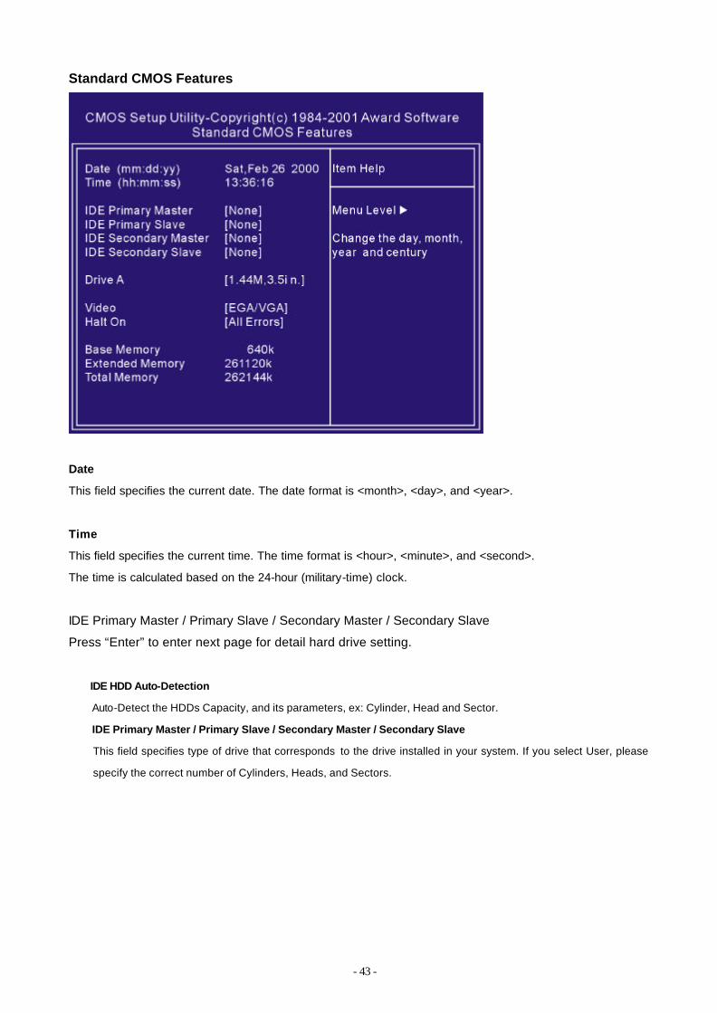
Standard CMOS Features
Date
This field specifies the current date. The date format is <month>, <day>, and <year>.
Time
This field specifies the current time. The time format is <hour>, <minute>, and <second>.
The time is calculated based on the 24-hour (military-time) clock.
IDE Primary Master / Primary Slave / Secondary Master / Secondary Slave
Press “Enter” to enter next page for detail hard drive setting.
IDE HDD Auto-Detection
Auto-Detect the HDDs Capacity, and its parameters, ex: Cylinder, Head and Sector.
IDE Primary Master / Primary Slave / Secondary Master / Secondary Slave
This field specifies type of drive that corresponds to the drive installed in your system. If you select User, please
specify the correct number of Cylinders, Heads, and Sectors.
- 44 -
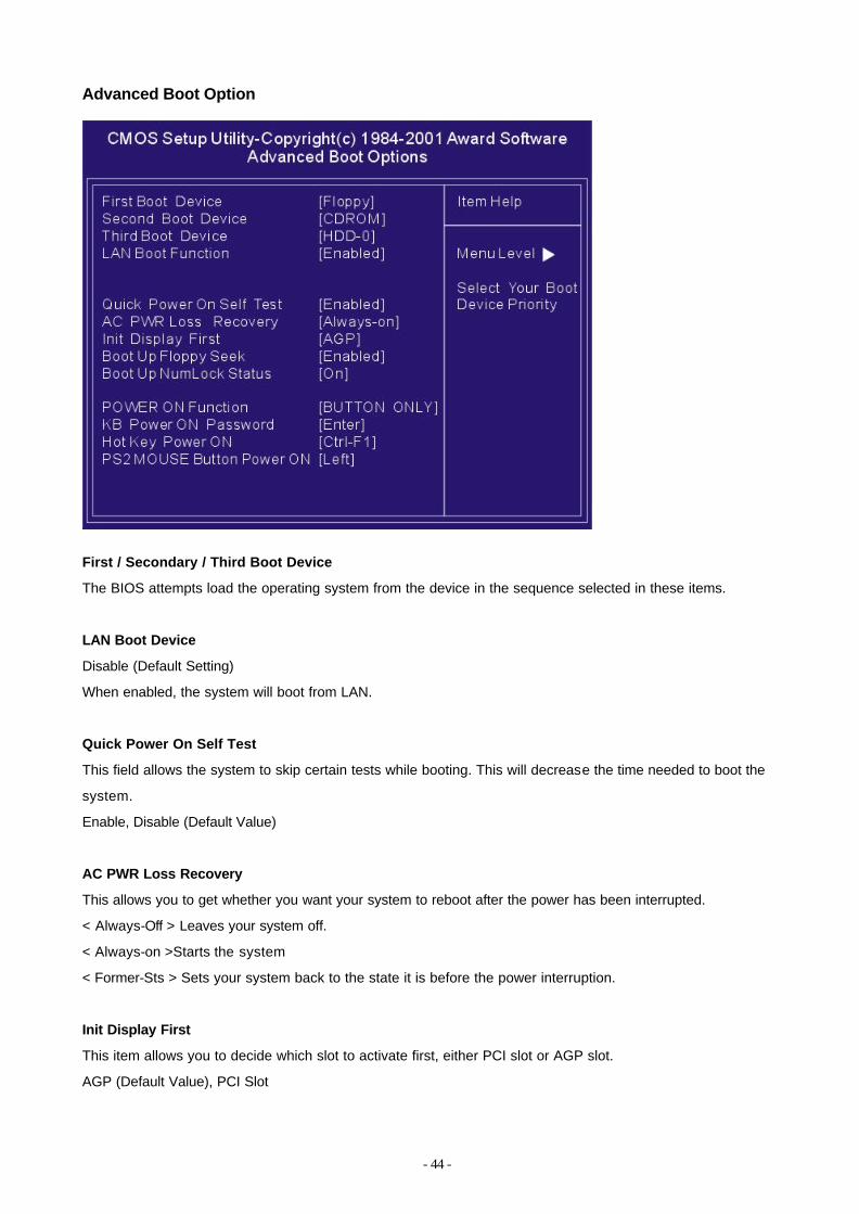
Advanced Boot Option
First / Secondary / Third Boot Device
The BIOS attempts load the operating system from the device in the sequence selected in these items.
LAN Boot Device
Disable (Default Setting)
When enabled, the system will boot from LAN.
Quick Power On Self Test
This field allows the system to skip certain tests while booting. This will decrease the time needed to boot the
system.
Enable, Disable (Default Value)
AC PWR Loss Recovery
This allows you to get whether you want your system to reboot after the power has been interrupted.
< Always-Off > Leaves your system off.
< Always-on >Starts the system
< Former-Sts > Sets your system back to the state it is before the power interruption.
Init Display First
This item allows you to decide which slot to activate first, either PCI slot or AGP slot.
AGP (Default Value), PCI Slot

- 45 -
Boot Up Floppy Seek
Seeks disk drives during boot up. Disabling speeds boot up.
Boot Up Num Lock Status
This field determines the configuration of the numeric keypad after system boot up. If open the keypad uses
numbers keys. If close the keypad uses arrow keys.
Power-on Function
This field configures the Power-on mode of the system.
The Power-on button will not function in this mode.
Password: You can assign a password string thru KB Power-On password field.
Hot KEY: You can assign a hot key through the Hot Key Power-On field. Pressing this hot key will power- on your
system.
Mouse/Password: Double-Clicking the mouse button or typing the KB power-on password will automatically power-on
your system
Mouse/Hot KEY: Double-Clicking the mouse button or typing the KB hot-key will power on your system
Any Key: Power On System by pressing any key on Keyboard.
Button only(Default Value): Simply power-on your system by pressing the Power-On button on the front panel of your
PC case
Keyboard 98: Enables Keyboard 98 function. The function is good only for users of Keyboard 98.
Keyboard Power-on Password
If you wish to use this function, bring the cursor to the field written Enter, then press <Enter>. The computer
will display the message, Enter Password Type your password and press <Enter>. After the message
Confirm Password is displayed, re-type your password. The KB Power-on function will be in effect after you
save and exit setup.
To disable a password, bring the cursor to the Enter field again, then press <Enter>. The computer will
display the message, Enter Password Press <Enter>. A message will confirm that the password is disabled.
Hot Key Power-on
This field specifies key selection for the Keyboard-Power-on hot key.
- 46 -
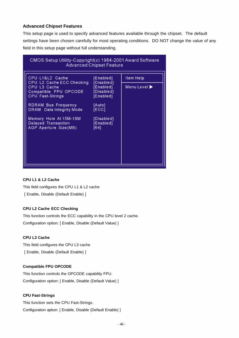
Advanced Chipset Features
This setup page is used to specify advanced features available through the chipset. The default
settings have been chosen carefully for most operating conditions. DO NOT change the value of any
field in this setup page without full understanding.
CPU L1 & L2 Cache
This field configures the CPU L1 & L2 cache
[ Enable, Disable (Default Enable) ]
CPU L2 Cache ECC Checking
This function controls the ECC capability in the CPU level 2 cache.
Configuration option: [ Enable, Disable (Default Value) ]
CPU L3 Cache
This field configures the CPU L3 cache
[ Enable, Disable (Default Enable) ]
Compatible FPU OPCODE
This function controls the OPCODE capability FPU.
Configuration option: [ Enable, Disable (Default Value) ]
CPU Fast-Strings
This function sets the CPU Fast-Strings.
Configuration option: [ Enable, Disable (Default Enable) ]

- 47 -
RDRAM Bus Frequency
This function sets frequency of RDRAM memory.
[Default is Auto ]
DRAM Data Integrity Mode
[Default is ECC ]
Memory Hole At 15M-16M
This function allows you to reserve an address space for others device that require it.
[Default is Disabled ]
Delayed Transaction
When enabled, the south bridge ICH2 will supports the Delayed Transaction mechanism when it is the target
of a PCI transaction.
[ Enable (Default Value), Disabled ]
AGP Aperture Size (MB)
This field configures the main memory size for AGP graphics data used.
64MB (Default Value)
Integrated Peripherals
- 48 -
IDE Primary Master / Slave UDMA
IDE Secondary Master / Slave UDMA
If you select Auto, the IDE controller uses Ultra DMA 33/66/100 Mode to access Ultra DMA-capable IDE
devices. Depend on the resent of negotiation with your HDD. The maximum transfer rate of Ultra DMA 100
Mode is 100 MB/sec.
[Auto , Disabled(Default Auto)]
Onboard SCSI Controller
On board SCSI controller for enabling / disabling onboard SCSI controller.
[ Enable , Disabled (Default Enable) ]
Onboard LAN Controller
This field enables or disables the onboard LAN controller.
[Enable, Disabled (Default Enable)]
Onboard FDC Controller
This field enables or disables the onboard floppy controller.
[Enable, Disabled (Default Enable)]
AC97 Audio
Auto ”allows the motherboard’s BIOS to detect whether you are using any AC97audio device. If a audio
device is detected, the onboard audio controller will be enabled. If no audio device is detected, the onboard
audio controller will be disabled. If you want to use different controller cards to connect audio connector, set
these fields to disabled
[ Disabled , Auto ( Default Value ) ]
USB Controller
Select Enabled if your system contains USB peripherals.
[ Enable, Disabled (Default Enable) ]
USB Legacy Support
Select Enabled if your system contains USB peripherals in Legacy mode.
[ Enable , Disabled (Default Value) ]
Onboard Serial Port 1 / 2
These fields configure the onboard serial ports. There are several port addresses and IRQ channels to
select from.
- 49 -
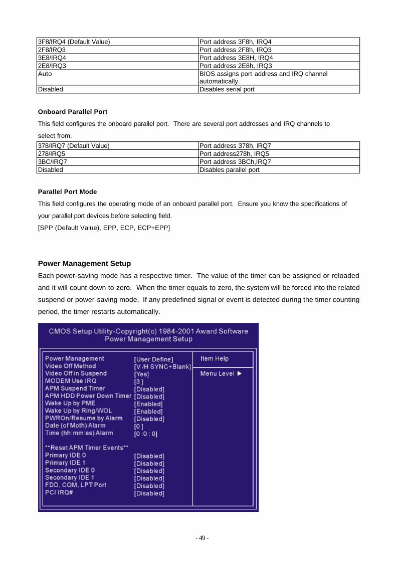
3F8/IRQ4 (Default Value) Port address 3F8h, IRQ4 2F8/IRQ3 Port address 2F8h, IRQ3 3E8/IRQ4 Port address 3E8H, IRQ4 2E8/IRQ3 Port address 2E8h, IRQ3 Auto BIOS assigns port address and IRQ channel
automatically. Disabled Disables serial port
Onboard Parallel Port
This field configures the onboard parallel port. There are several port addresses and IRQ channels to
select from.
378/IRQ7 (Default Value) Port address 378h, IRQ7 278/IRQ5 Port address278h, IRQ5 3BC/IRQ7 Port address 3BCh,IRQ7 Disabled Disables parallel port
Parallel Port Mode
This field configures the operating mode of an onboard parallel port. Ensure you know the specifications of
your parallel port devi ces before selecting field.
[SPP (Default Value), EPP, ECP, ECP+EPP]
Power Management Setup
Each power-saving mode has a respective timer. The value of the timer can be assigned or reloaded
and it will count down to zero. When the timer equals to zero, the system will be forced into the related
suspend or power-saving mode. If any predefined signal or event is detected during the timer counting
period, the timer restarts automatically.

- 50 -
Power Management
This feature allows the user to select the default parameters for the power-saving mode.
Min saving When idle for one hour, the system enter suspend mode
Max Saving
When idle for fifteen minutes, the system enters suspend mode.
User Define (Default Value)
User can specify the time the system enter suspend mode.
Video off Method
V/H SYNC +Blank (Default Value ) Turn off the vertical and horizontal synchronization ports and write blanks to the video buffer.
Blank Screen Writes blanks to the video buffer only. DPMS Initial display power management signaling with
DPMS.
Video Off In Suspend
This determines the manner in which the monitor is blanked.
[NO, Yes (Default Value)]
MODEM Use IRQ
This determines the IRQ in which the MODEM can use.
[ 3(Default Value),4,5,7,9,11,NA]
APM Suspend Timer
This field specifies the time the system enters power-saving mode. It is available only when the Power
Management field is set to User Define.
[1Min, 2Min, 4Min, 8Min, 12Min, 20Min, 30Min, 40Min, 1Hour,Disablet (Default Value)]
APM HDD Power Down Timer
This field specifies the time the system enters HDD power down. It is available only when the Power
Management field is set to User Define.
[1Min, 2 Min, 3Min, 4Min, 5 Min, 6 Min, 7 Min , 8Min, 9 Min , 10 Min, 11 Min, 12 Min, 13Min,14 Min, 15 Min,
Disable (Default Value) ]
Wake up by PME
Wake up by PME, PME (Power Management Enable) signal
[Enabled, Disabled (Default Enabled)]
Wake up by RING/WOL
When WOL (Wake On LAN) function is enabled, the PC can power-on or ” Wake up” ? through
LAN (Local Area Network ). When Wake up by RING function is enabled, the PC can power-on through the
LAN adapter connected should be connected to the WOL header on the motherboard.
- 51 -
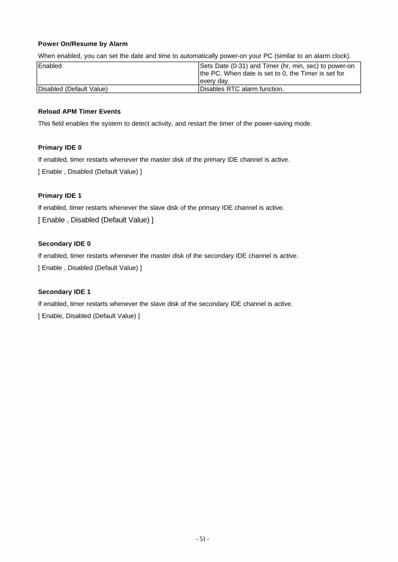
Power On/Resume by Alarm
When enabled, you can set the date and time to automatically power-on your PC (similar to an alarm clock).
Enabled Sets Date (0-31) and Timer (hr, min, sec) to power-on the PC. When date is set to 0, the Timer is set for every day.
Disabled (Default Value) Disables RTC alarm function.
Reload APM Timer Events
This field enables the system to detect activity, and restart the timer of the power-saving mode.
Primary IDE 0
If enabled, timer restarts whenever the master disk of the primary IDE channel is active.
[ Enable , Disabled (Default Value) ]
Primary IDE 1
If enabled, timer restarts whenever the slave disk of the primary IDE channel is active.
[ Enable , Disabled (Default Value) ]
Secondary IDE 0
If enabled, timer restarts whenever the master disk of the secondary IDE channel is active.
[ Enable , Disabled (Default Value) ]
Secondary IDE 1
If enabled, timer restarts whenever the slave disk of the secondary IDE channel is active.
[ Enable, Disabled (Default Value) ]
- 52 -
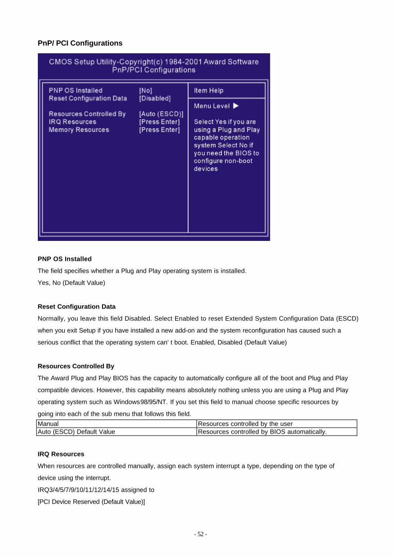
PnP/ PCI Configurations
PNP OS Installed
The field specifies whether a Plug and Play operating system is installed.
Yes, No (Default Value)
Reset Configuration Data
Normally, you leave this field Disabled. Select Enabled to reset Extended System Configuration Data (ESCD)
when you exit Setup if you have installed a new add-on and the system reconfiguration has caused such a
serious conflict that the operating system can‘t boot. Enabled, Disabled (Default Value)
Resources Controlled By
The Award Plug and Play BIOS has the capacity to automatically configure all of the boot and Plug and Play
compatible devices. However, this capability means absolutely nothing unless you are using a Plug and Play
operating system such as Windows98/95/NT. If you set this field to manual choose specific resources by
going into each of the sub menu that follows this field.
Manual Resources controlled by the user Auto (ESCD) Default Value Resources controlled by BIOS automatically.
IRQ Resources
When resources are controlled manually, assign each system interrupt a type, depending on the type of
device using the interrupt.
IRQ3/4/5/7/9/10/11/12/14/15 assigned to
[PCI Device Reserved (Default Value)]
- 53 -
DMA Resources
This sub menu can let you control the memory resource.
Reserved Memory Base
Reserved a low memory for the legacy device (non-PnP device).
[C800, CC00, D000, D800, DC400, N/A (Default Value)]
Reserved Memory Length
Reserved a low memory length for the legacy device (non-PnP device).
[8K (Default Value), 16K, 32K, 64K]
Security Features
Set Supervisor / User Password Setting
These setup pages are used for password setting. When a password has been enabled and the
Security Option field is set as Setup, you will be required to enter the password every time you try to
enter BIOS Setup program. This prevents an unauthorized person from changing any part of your
system configuration. Additionally, if the Security Option field is set as Boot, the BIOS will request a
password every time your system boot. This would prevent unauthorized use of your computer.
If you wish to use this function, bring the cursor to this field, then press <Enter>. The computer will
display the message, ”Enter Password “ Type your password and press <Enter>. After the message on
firm Password is displayed, re-type your password. The Supervisor Password function will be in effect
after you save and exit setup.
- 54 -
To disable a password, bring the cursor to this field, then press <Enter>. The computer will display the
message, ”Enter Password ”. Press <Enter>. A message will confirm that the password is disabled.
Once the password is disabled, the system will boot and you can enter setup program freely.
CPU Smart Setting
CPU smart setting provides users a fuss free CPU frequency set up procedure.
Selecting probably CPU Frequency by < +PU / -PD>
- 55 -
PC Health Status
This page is monitoring your status of computer. On the screen display CPU/System temperature, FAN
speed, and voltages.
Load Fail-Safe Defaults
When you press <Enter> on this item. You get a confirmation dialog box with a message similar to:
Press “Y” loads the default values that are factory settings for optimal performance system operations.
- 56 -
Load Optimized Defaults
When you press <Enter> on this item. You get a confirmation dialog box with a message similar to:
Press “Y” loads the default values that are factory settings for optimal performance system operations.
Save & Exit Setup
When you press <Enter> on this item. You get a confirmation dialog box with a message similar to:
Press “Y” saves current CMOS value and exit BIOS setup program
- 57 -
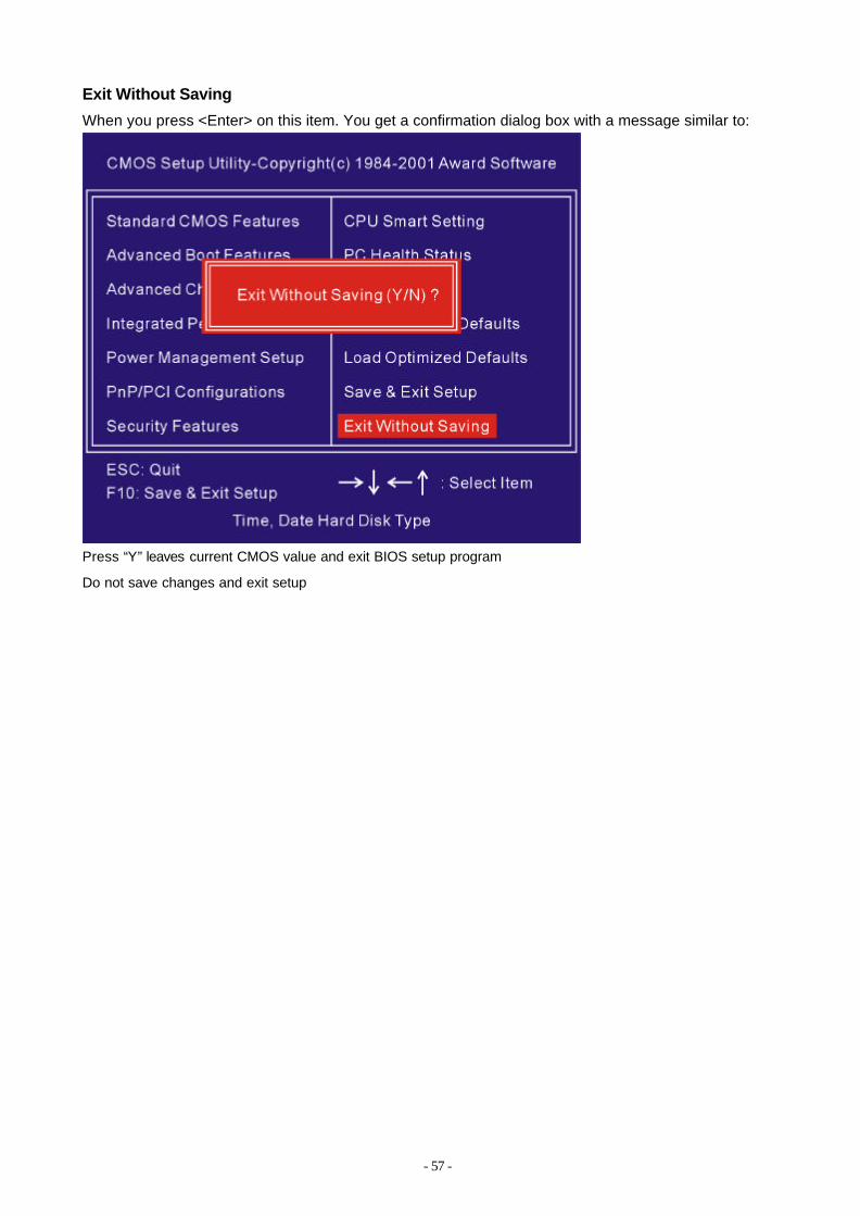
Exit Without Saving
When you press <Enter> on this item. You get a confirmation dialog box with a message similar to:
Press “Y” leaves current CMOS value and exit BIOS setup program
Do not save changes and exit setup
- 58 -
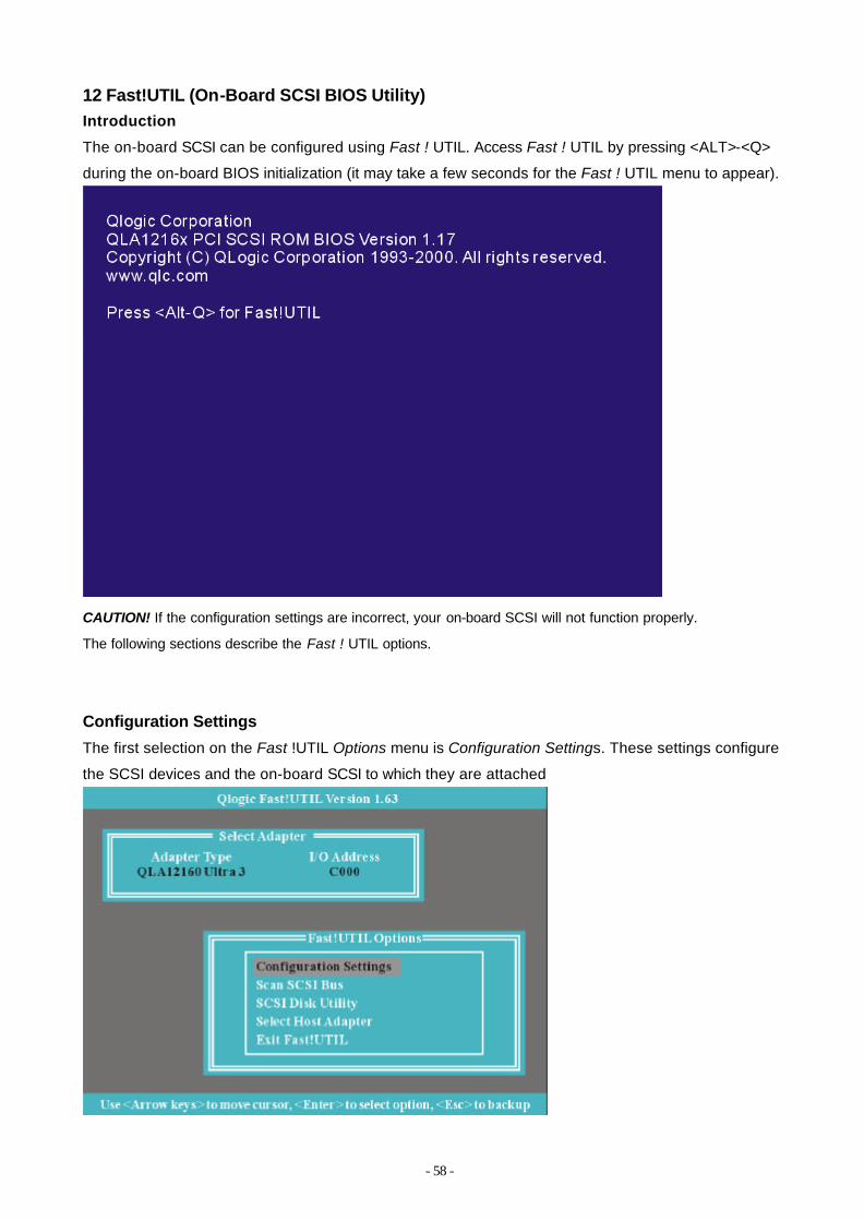
12 Fast!UTIL (On-Board SCSI BIOS Utility) Introduction
The on-board SCSI can be configured using Fast ! UTIL. Access Fast ! UTIL by pressing <ALT>-<Q>
during the on-board BIOS initialization (it may take a few seconds for the Fast ! UTIL menu to appear).
CAUTION! If the configuration settings are incorrect, your on-board SCSI will not function properly.
The following sections describe the Fast ! UTIL options.
Configuration Settings
The first selection on the Fast !UTIL Options menu is Configuration Settings. These settings configure
the SCSI devices and the on-board SCSI to which they are attached
- 59 -
Host Adapter Settings
From the Configuration Settings menu in Fast ! UTIL, select Host Adapter Settings.
The default settings for the on-board SCSI host are listed in table A-1 and described in the following
paragraphs
Table A-1. Host Adapter Settings
Setting Options Default
Host adapter BIOS PCI DMA burst CDROM Boot Adapter Configuration Drivers Load RISC code >4Gbyte Addressing Fast Command Posting
Enabled or Disabled Enabled or Disabled Enabled or Disabled Auto, Manual, Safe Enabled or Disabled Enabled or Disabled Enabled or Disabled
Enabled Enabled Disabled Auto Enabled Disabled Enabled
Host adapter BIOS. When this setting is disabled, the ROM BIOS on the On-board SCSI is disabled, freeing space in
upper memory. The RAM BIOS and other drivers still recognize the On-board SCSI.
Do not disable this setting if you are booting from a SCSI disk drive attached to the On-board SCSI. The default is
Enabled.
PCI bus DMA burst. When this setting is enabled, burst transfers are performed. When this setting is disabled, data is
transferred in nonburst mode, with each cycle initiated by a new address phase. The default is Enabled.
CDROM Boot. When this setting is enabled, the ROM BIOS boots from the attached SCSI CD-ROM if a bootable
compact disk is installed. If no bootable CD-ROM is found, the system boots from the first bootable SCSI drive. When
this setting is disabled, the ROM BIOS does not boot from the CD-ROM. The default is Disabled.
Drivers Load RISC code. When this setting is enabled, the On-board SCSI uses the RISC firmware that is embedded in
the software driver. When this setting is disabled, the software driver loads the latest version of RISC firmware found on
the system. The default is Enabled.
NOTE: The driver being loaded must support this setting. If the driver does not support this setting, the result is
the same as disabled regardless of the setting. Leaving this option enabled guarantees a certified combination
of software driver and RISC firmware.
Scan and Configure SCSI Devices
NOTE: You must set the Adapter Configuration setting in the Host Adapter Settings to Manual to use Auto
configure; otherwise, all changes made with Auto-configure are reset when your system is rebooted.
- 60 -
The on-board SCSI is designed to sense and configure the devices connected to your motherboard. With he
Adapter Configuration set to Manual, the Auto-configure option gives you control of when the bus is scanned
and configured. Selecting the Auto-configure SCSI Devices option from the Configuration Settings menu
causes the on-board SCSI to scan the devices on the SCSI bus and set the following options, based on the
capabilities of each device:
Enable Device Negotiate Wide Tagged Queuing Disconnects Negotiate Synchronous Enable LUN Support
If you use Auto configure to configure your system, you should run Fast ! UTIL and select “Auto configure”
SCSI Devices after adding or reconfiguring devices attached to the on-board SCSI.
Selectable Boot Settings
The Selectable Boot Settings option is accessed from the Configuration Settings menu. If you enable this
option, you can select the SCSI ID from which you want to boot. SCSI ID values range from 0-15. Once
enabled, this option forces the system to boot on the selected SCSI drive, ignoring any IDE drives attached
to your system. If you disable this option, the system looks for an IDE drive from which to boot. If an IDE
drive is not found, the system looks for the first bootable SCSI drive. In disabled mode, the SCSI Boot ID and
SCSI Boot LUN parameters have no effect.
NOTE: This option applies only to disk devices; it does not apply to CD-ROMs, tape drives, and other
non-disk devices.
Restore Default Adapter Settings
The Restore Defaults option from the Configuration Settings menu restores the on-board SCSI default
settings. The default settings are displayed on the SCSI Device Settings screen. Use the arrow keys to
change the settings.
Raw NVRAM Data
This option displays the adapter’s nonvolatile random access memory (NVRAM) contents in hexadecimal
format. This is a troubleshooting tool; you cannot modify the data.
- 61 -
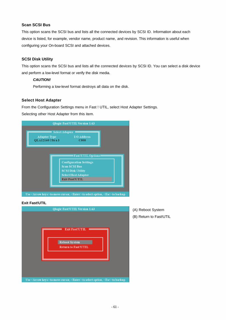
Scan SCSI Bus
This option scans the SCSI bus and lists all the connected devices by SCSI ID. Information about each
device is listed, for example, vendor name, product name, and revision. This information is useful when
configuring your On-board SCSI and attached devices.
SCSI Disk Utility
This option scans the SCSI bus and lists all the connected devices by SCSI ID. You can select a disk device
and perform a low-level format or verify the disk media.
CAUTION!
Performing a low-level format destroys all data on the disk.
Select Host Adapter
From the Configuration Settings menu in Fast ! UTIL, select Host Adapter Settings.
Selecting other Host Adapter from this item.
Exit Fast!UTIL
(A) Reboot System
(B) Return to Fast!UTIL
- 62 -
13 Appendix Beep Codes
Currently there are two kinds of beep codes in BIOS. This code indicates that a video error has
occurred and the BIOS cannot initialize the video screen to display any additional information. This
beep code consists of a single long beep followed by three short beeps. The other code indicates that
your DRAM error has occurred. This beep code consists of a single long beep repeatedly.
BIOS Protection / Auto Recovery Feature
BIOS Protection:
There is one jumper (JP16) located at between the two PCI-64 slots (PCI64_1 and PCI64_2). When
you installed the jumper at 1-2, it means the FWH is protected or unprotected depend on the bios
setting. When you installed the jumper at 2-3, it means that the FHW is always protected from H/W. The
default state is at 1-2.
There is an option (BIOS-ROM Flash Protect) in the bios setup. The option is only available when the
JP16 is installed at 1-2. If you select “Non-Flash”, the FWH will be protected from any write action or
virus. If you select “Flashable”, the FWH is unprotected and allowed to update the content with flash
utility. Below is the way to test the function is worked or not:
(1) When jumper (JP16) is at 1-2: Please check your setting in the bios setup. If the setting is “Non-Flash”, all write
action to the FHW will be unacceptable. The contents in the FWH will not changed by the flash utility. If the setting is
“Flashable”, you can update the new content to the FWH from flash utility.
(2) When jumper (JP16) is at 2-3: No matter the setting in the bios setup is “Non-Flash” or “Flashable”, the contents
in the FWH will not changed always .
Auto Recovery Feature:
The feature is functioned when you update bios failure or some unexpected conditions (like AC power
lost suddenly ) . The bios will still alive and allowed to update again.
- 63 -
AWARD BIOS POST CONTROL FLOW
09h Reserved 0Ah 1. Disable PS/2 mouse interface (optional).
2. Auto detect ports for keyboard & mouse followed by a port & interface swap (optional).
3. Reset keyboard for Winbond 977 series Super I/O chips. 0Bh Reserved 0Ch Reserved 0Dh Reserved 0Eh Test F000h segment shadow to see whether it is R/W -able or not. If test
fails, keep beeping the speaker. 0Fh Reserved 10h Auto detect flash type to load appropriate flash R/W codes into the
run time area in F000 for ESCD & DMI support. 11h Reserved 12h Use walking 1’s algorithm to check out interface in CMOS circuitry. Also
set real-time clock power status, and then check for override. 13h Reserved 14h Program chipset default values into chipset.
Chipset default value is MODBINable by OEM customers. 15h Reserved 16h Initial onboard clock generator if Early_Init_Onboard_Generator
Is defined. See also POST 26h
POST (hex) Description CFh Test CMOS R/W functionality. C0h Early chipset initialization:
-Disable shadow RAM -Disable L2 cache (socket 7 or below) -Program basic chipset registers
C1h Detect memory - Auto-detection of DRAM size, type and ECC.
Auto-detection of L2 cache (socket 7 or below) C3h Expand compressed BIOS code to DRAM C5h Call chipset hook to copy BIOS back to E000 & F000
Shadow RAM. 01h Expand the Xgroup codes locating in physical address
1000:0 02h Reserved 03h Initial Superio_Early_Init 04h Reserved 05h 1. Blank out screen
2. Clear CMOS error flag 06h Reserved 07h 1. Clear 8042 interface
2. Initialize 8042 self-test 08h 1. Test special keyboard controller for Winbond 977 series
Super I/O chips. 2. Enable keyboard interface.
- 64 -
17h Reserved 18h Detect CPU information including brand, SMI type (Cyrix or Intel) and
(CPU level (586 or 686). 19h Reserved 1Ah Reserved 1Bh Initial interrupts vector table. If no special specified, all H/W
Interrupts are directed to SPURIOUS_INT_HDLR & S/W Interrupts to SPURIOUS_soft_HDLR.
1Ch Reserved 1Dh Initial EARLY_PM_INIT switch. 1Eh Reserved 1Fh Load keyboard matrix (notebook platform) 20h Reserved 21h HPM initialization (notebook platform) 22h Reserved 23h 1. Check validity of RTC value:
e.g. a value of 5Ah is an invalid value for RTC minute. 2 . Load CMOS settings into BIOS stack. If CMOS checksum fail , use default value instead.
24h Prepare BIOS resource map for PCI & PnP use. If ESCD is valid, take into consideration of the ESCD’s legacy information.
25h Early PCI initialization: - Enumerate PCI bus number - Assign memory & I/O resource - Search for a valid VGA device & VGA BIOS, and put it into C000:0.
26h 1. If Early_Init_Onboard_Generator is not defined Onboard clock generator initialization. Disable respective Clock resource to empty PCI & DIMM slots.
1. Init onboard PWM 2. Init onboard H/W monitor devices
27h Initialize INT 09 buffer 28h Reserved 29h 1. Program CPU internal MTRR (P6 & PII) for 0-640K memory address.
2. Initialize the APIC for Pentium class CPU. 3. Program early chipset according to CMOS setup. Example: onboard
IDE controller. 4. Measure CPU speed.
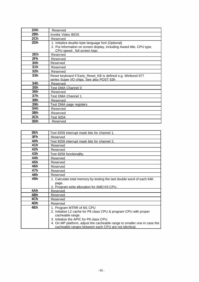
- 65 -
3Eh Test 8259 interrupt mask bits for channel 1. 3Fh Reserved 40h Test 8259 interrupt mask bits for channel 2. 41h Reserved 42h Reserved 43h Test 8259 functionality. 44h Reserved 45h Reserved 46h Reserved 47h Reserved 48h Reserved 49h 1. Calculate total memory by testing the last double word of each 64K
page. 2. Program write allocation for AMD K5 CPU.
4Ah Reserved 4Bh Reserved 4Ch Reserved 4Dh Reserved 4Eh 1. Program MTRR of M1 CPU
2. Initialize L2 cache for P6 class CPU & program CPU with proper cacheable range.
3. Initialize the APIC for P6 class CPU. 4. On MP platform, adjust the cacheable range to smaller one in case the
cacheable ranges between each CPU are not identical.
2Ah Reserved 2Bh Invoke Video BIOS 2Ch Reserved 2Dh 1. Initialize double-byte language font (Optional)
2. Put information on screen display, including Award title, CPU type, CPU speed , full screen logo
2Eh Reserved 2Fh Reserved 30h Reserved 31h Reserved 32h Reserved 33h Reset keyboard if Early_Reset_KB is defined e.g. Winbond 977
series Super I/O chips. See also POST 63h 34h Reserved 35h Test DMA Channel 0 36h Reserved 37h Test DMA Channel 1 38h Reserved 39h Test DMA page registers 3Ah Reserved 3Bh Reserved 3Ch Test 8254 3Dh Reserved
- 66 -
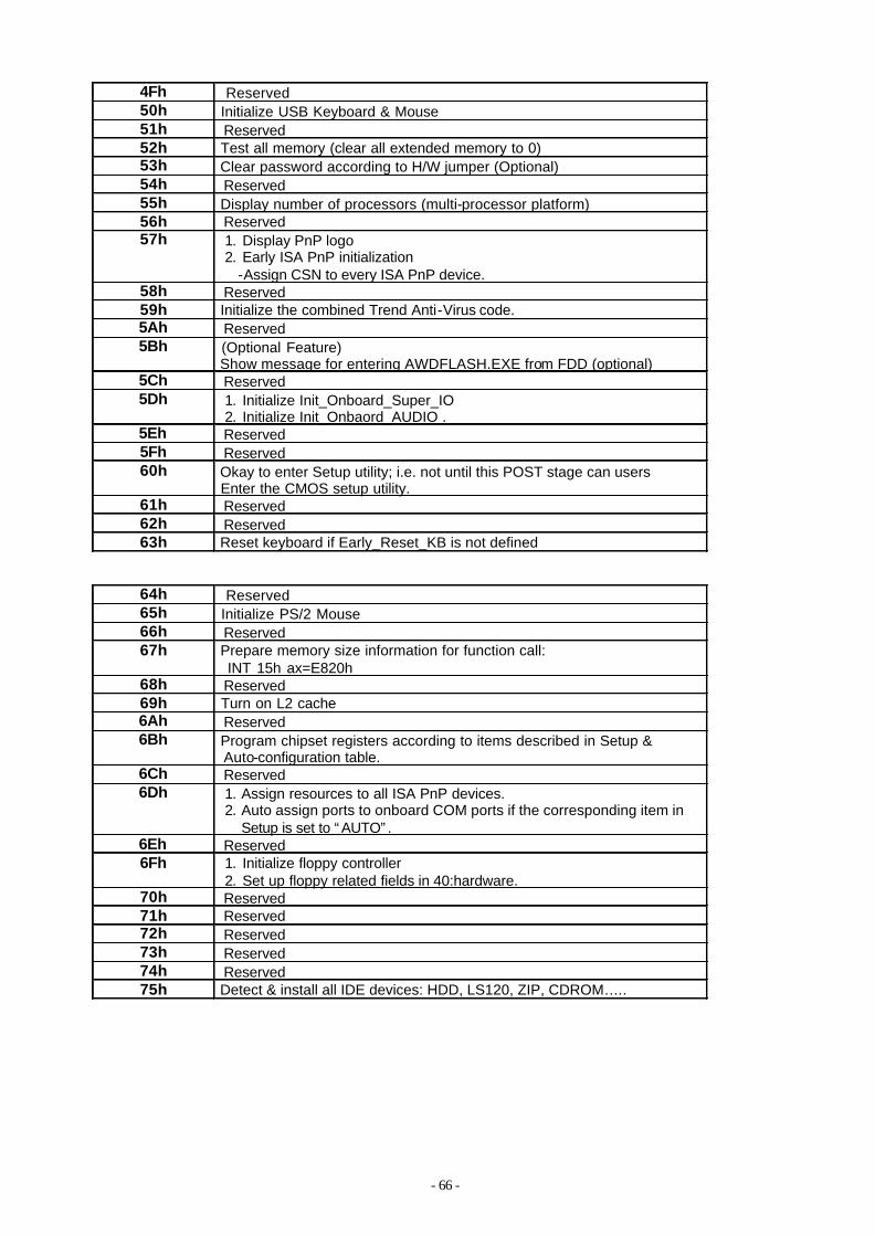
4Fh Reserved 50h Initialize USB Keyboard & Mouse 51h Reserved 52h Test all memory (clear all extended memory to 0) 53h Clear password according to H/W jumper (Optional) 54h Reserved 55h Display number of processors (multi-processor platform) 56h Reserved 57h 1. Display PnP logo
2. Early ISA PnP initialization -Assign CSN to every ISA PnP device.
58h Reserved 59h Initialize the combined Trend Anti-Virus code. 5Ah Reserved 5Bh (Optional Feature)
Show message for entering AWDFLASH.EXE from FDD (optional) 5Ch Reserved 5Dh 1. Initialize Init_Onboard_Super_IO
2. Initialize Init_Onbaord_AUDIO . 5Eh Reserved 5Fh Reserved 60h Okay to enter Setup utility; i.e. not until this POST stage can users
Enter the CMOS setup utility. 61h Reserved 62h Reserved 63h Reset keyboard if Early_Reset_KB is not defined
64h Reserved 65h Initialize PS/2 Mouse 66h Reserved 67h Prepare memory size information for function call:
INT 15h ax=E820h 68h Reserved 69h Turn on L2 cache 6Ah Reserved 6Bh Program chipset registers according to items described in Setup &
Auto-configuration table. 6Ch Reserved 6Dh 1. Assign resources to all ISA PnP devices.
2. Auto assign ports to onboard COM ports if the corresponding item in Setup is set to “AUTO”.
6Eh Reserved 6Fh 1. Initialize floppy controller
2. Set up floppy related fields in 40:hardware. 70h Reserved 71h Reserved 72h Reserved 73h Reserved 74h Reserved 75h Detect & install all IDE devices: HDD, LS120, ZIP, CDROM… ..
- 67 -
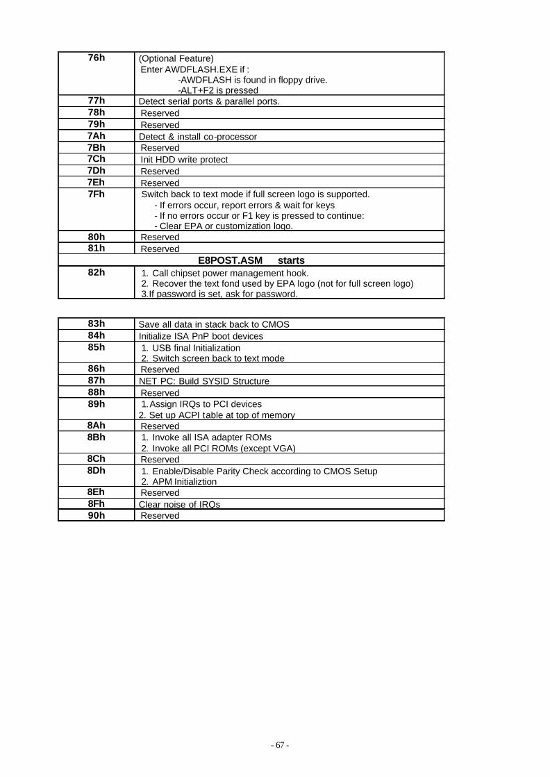
76h (Optional Feature) Enter AWDFLASH.EXE if : -AWDFLASH is found in floppy drive. -ALT+F2 is pressed
77h Detect serial ports & parallel ports. 78h Reserved 79h Reserved 7Ah Detect & install co-processor 7Bh Reserved 7Ch Init HDD write protect 7Dh Reserved 7Eh Reserved 7Fh Switch back to text mode if full screen logo is supported.
- If errors occur, report errors & wait for keys - If no errors occur or F1 key is pressed to continue: - Clear EPA or customization logo.
80h Reserved 81h Reserved
E8POST.ASM starts 82h 1. Call chipset power management hook.
2. Recover the text fond used by EPA logo (not for full screen logo) 3.If password is set, ask for password.
83h Save all data in stack back to CMOS 84h Initialize ISA PnP boot devices 85h 1. USB final Initialization
2. Switch screen back to text mode 86h Reserved 87h NET PC: Build SYSID Structure 88h Reserved 89h 1. Assign IRQs to PCI devices
2. Set up ACPI table at top of memory 8Ah Reserved 8Bh 1. Invoke all ISA adapter ROMs
2. Invoke all PCI ROMs (except VGA) 8Ch Reserved 8Dh 1. Enable/Disable Parity Check according to CMOS Setup
2. APM Initializtion 8Eh Reserved 8Fh Clear noise of IRQs 90h Reserved
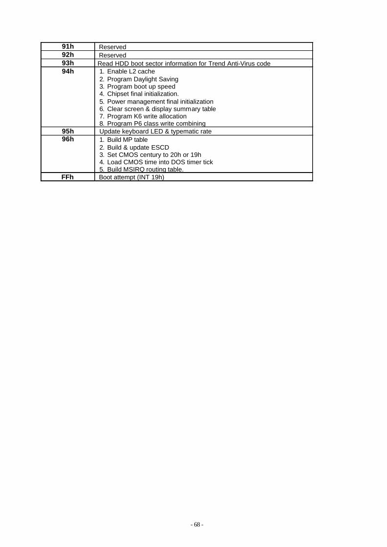
- 68 -
91h Reserved 92h Reserved 93h Read HDD boot sector information for Trend Anti-Virus code 94h 1. Enable L2 cache
2. Program Daylight Saving 3. Program boot up speed 4. Chipset final initialization. 5. Power management final initialization 6. Clear screen & display summary table 7. Program K6 write allocation 8. Program P6 class write combining
95h Update keyboard LED & typematic rate 96h 1. Build MP table
2. Build & update ESCD 3. Set CMOS century to 20h or 19h 4. Load CMOS time into DOS timer tick 5. Build MSIRQ routing table.
FFh Boot attempt (INT 19h)