Embed Size (px)
Citation preview

TRANSIENT TUNNELING CURRENTS IN NEAR-SURFACE QUANTUM WELLS
B. BONANNI, M. CAPIZZI, R. DIOLETIA, V. EMILIANI, A. FROV A, and C. PRESILLA
Dip. di Fisica, Universita "La Sapienza", Piazzale A. Moro 2, 00185 Roma, Italy
M. COLOCCI, M. GURIOLI, and A. VINA TIIERI LENS Laboratory, Universita di Firenze, Largo E. Fermi 2, 50125 Firenze, Italy
F. MARTELLI Fondazione Ugo Bordoni, via B. Castiglione 59, 00142 Roma, ilaly
Y.-L. CHANG, J. L. MERZ, and S.-S. STONE QUEST Center, University of California, Santa Barbara, CA 93106
ABSTRACT
Continuous-wave and time-resolved photoluminescence at low temperatures is investigated in near-surface quantum wells, where carrier tunneling to surface states reduces the el-hhl excitonic emission efficiency. Analysis of the time-resolved spectra points to a behavior for strained InGaAs/GaAs structures different from AlGaAs/GaAs interfaces, in that tunneling occurs not only from the free-carrier continuum, but also from the exciton ground state.
1043
In low-dimensional structures, having high surface-to-volume ratio, the electrical and optical behavior is strongly affected by the surface. For example, in a quantum well (QW) built next to the surface, an extra recombination channel opens if electrons and holes can tunnel to surface states (SS). As a consequence, the QW emission efficiency can drop significantly. The dependence of this effect on surface-barrier thickness has been investigated by steady-state photoluminescence (CW-PL) in Alo.3Gao.7As/GaAsl,2 and lnxGal-xAs/GaAs quantum structures.3·4 As observed5 and theoretically explained,6 the difference between tunneling times for electrons and holes - shorter for holes - induces an electric field, enabling an ambipolar-tunneling regime. Time-resolved PL (TR-PL) from near-surface QWs can give information about the details of tunneling, e.g., if electrons and holes tunnel to SS before or after exciton formation and - in the latter case - if they tunnel as an exciton complex or otherwise. The decay time of the free-exciton in AIGaAs/GaAs QWs turns out to be nearly independent of the surface barrier thickness,5 suggesting that tunneling occurs only prior to exciton formation. The purpose of this work is a more detailed analysis of the TR-PL spectra, both the rise and the decay phases. The study is extended to Alo.3Gao.7As/GaAs structures different from those used in Ref. 5 in terms of

1044 B. Bonanni et al.
well width and surface treatment. For their basically different behavior, strained lno.tGao.9As/GaAs QWs are also investigated.
All the structures used (see Table 1) have a near-surface QW (SW), at various distances from the surface, separated (by barrier II) from a deeper reference well (RW), used for normalization of the PL emission from the SW (NPL). CW-PL spectra at 5K were taken using excitation energy below the bandgap of the barrier. TR-PL spectra at the elhhl exciton peak were measured at - 12K by pumping with 5-ps pulses from a dye-laser, with a repetition rate of 76 MHz, and using a streak camera for detection. Different barrier
Table I. Sample structures (thickness values are in nanometers).
Sample group Materials
(a) AlGaAs/GaAs (b) gy (b) 8YE
(c) InGaAs/GaAs
Surface barrier thickness d
35-3 (by etching of surface barrier) 8 (as grown, 0.5 GaAs cap)
8 (cap layer etched away) 70-9 (as grown, no cap layer)
SW Barrier II RW
6 350 10 10 350 7 10 350 7 11 100 7
thicknesses in samples of group (a), all from one wafer, were obtained by etching in a citric acid/H peroxide solution. Sample 8Y and samples from group (c) are as grown, the 8Y sample having a 0.5-nm-thick GaAs topping the AIGaAs surface barrier. Sample 8YE has been obtained from 8Y by removing the GaAs cap layer. Figure 1 shows the NPL 1.2 r----- -------- ---..., variation with surface barrier thickness d of the el-hhl transition for the above structures.As can be seen , tunneling to SS strongly reduces the PL efficiency for d ~ 120A (180A) in the unstrained (strained) interfaces. Comparison of the NPL from samples 8Y and 8YE readily proves that the GaAs cap layer strongly reduces tunneling toSS.
0.8
0.4
T· SK BY e
A , ee_,.-B--B-t~--~----e Q 0 0 •
8YE 1
rP
I o (a) I)
• (c)
10 20 30 40 50 60 70 barrier thickness (nm)
80
Figure I. NPL vs surface barrier thickness for unstrained (groups (a), (b)) and strained structures (group (c)). The lines are calculated from the theory in Ref. 6, predicting a readier fall of NPL when the tunneling barriers are thinner. The open circles are earlier published data, I shown here for comparison with the newlygrown AIGaAs/GaAs samples. The excitation wavelengths are 754 nm for group (a) , 700 nm for group (b), and 830 nm for group (c), with power density 0.5, 13.6. Ill W/cm2 respectively.
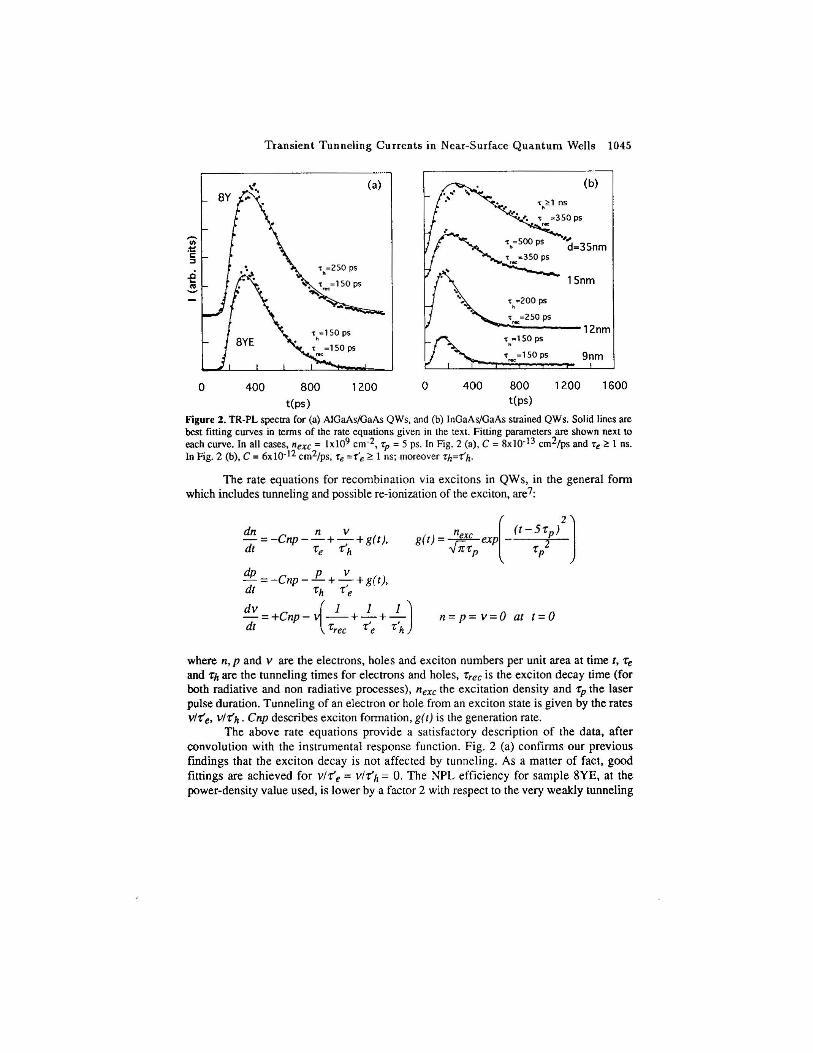
In Fig. 2 (a), we show the TR-PL spectra for the most significant AIGaAs/GaAs samples. Figure 2 (b) gives the behavior of strained InGaAs/GaAs QWs.
Transient Tunneling Currents in Near-Surface Quantum Wells 1045
(a)
'• - 250 ps lSnm
.. - 200 ps
t ,K - 250 ps
12nm •,-150ps
•~-150ps 9nm
0 400 800 1200 0 400 BOO 1200 1600
t(ps) t(ps)
Figure 2. TR-PL spectra for (a) AIGaAs/GaAs QWs, and (b) lnGaAs/GaAs strained QWs. Solid lines are best fitting curves in terms of the rate equations given in the text Fitting parameters are shown next lO each curve. In all cases, nexc = lxJ09 cm-2, fp = 5 ps. In Fig. 2 (a), C = 8xJ0·13 cm2/ps andre;::>: Ins. In Fig. 2 (b), C = 6xi0·12 cm2/ps, fe =t'e ;::>: 1 ns; moreover T:IJ=t'h ·
The rate equations for recombination via excitons in QWs, in the general form which includes tunneling and possible re-ionization of the exciton, are 7:
dn n v - = -Cnp--+ -,- + g(t), dt 're 'r h ( 2] n (t-5-r )
g(t) = --7J!Lexp - { "Tr:'rp 'rp
dp p v -= - Cnp--+-, +g(t), dt 'r!J 're
dv = +Cnp _ {-1-+ -4-+ -4-) dt 'rrec 'r e 'r h
n = p = v = 0 at t = 0
where n, p and v are the electrons, holes and exciton numbers per unit area at time t, 're and "riJ are the tunneling times for electrons and holes, "rrec is the exciton decay time (for both radiative and non radiative processes), nexc the excitation density and 'rp the laser pulse duration. Tunneling of an electron or hole from an exciton state is given by the rates vi'C'e. vf'(h . Cnp describes exciton formation, g(t) is the generation rate.
The above rate equations provide a satisfactory description of the data, after convolution with the instrumental response function. Fig. 2 (a) confirms our previous findings that the exciton decay is not affected by tunneling. As a matter of fact, good fittings are achieved for vi'C'e = vl-r'h = 0. The NPL efficiency for sample 8YE, at the power-density value used, is lower by a factor 2 with respect to the very weakly tunneling

1046 B. Bonanni et al.
sample 8Y (see Fig. 1), whilst 'free is virtually the same. Tunneling shows up as a shortening of the hole tunneling time, 150 against 250 ps.
The InGaAs/GaAs data in Fig. 2 (b) behave quite differently. The exciton decay time drops along with the hole tunneling time and the measured NPL in Fig. 1. It appears as if, possibly due to the presence of strain and/or interfacial defects, excitons and/or individual carriers from an exciton state can tunnel toward the surface and recombine in a way other than radiative emission in the well. In this process, the proximity of the surface plays a key role. Lower tunneling barriers and interfacial electric fields may also play a role. At least two features of the InGaAs/GaAs interface are not observed in AIGaAs/GaAs: i) accumulation of hydrogen, with appearance of an emission line,8 and TEM detection of H platelets in the limit of high H dosage,9 which is suggestive of important local disorder; ii) evidence of exciton trapping at interfacial disorder.IO
In conclusion, TR-PL in near-surface QWs has been measured and fitted with the aim of sheding light on the competition of exciton formation and/or tunneling to SS. This depends remarkably on sample structure and surface quality. In unstrained material, the dominant process involves tunneling of free carriers before they bind into excitons, so that exciton decay is independent of surface proximity. In strained material, the dynamics of the process is more complicated, with an appreciable coupling, for thin barriers, of the exciton to the surface and the opening of an extra channel for excitonic decay, with a shortening of the recombination time running in parallel to the NPL drop.
The work at Fondazione Bordoni has been carried out within the agreement with the Italian P.T. Administration.
References
l. Y.-L. Chang, I.-H. Tan, Y.-H. Zhang, J. Merz, E. Hu, A. Frova, and V. Emiliani, App/. Phys. Lett. 62, 2697 (1993). 2. J. M. Maison, K. Elcess, F. Houzay, J. Y. Marzin, J. M. Gerard, F. Barthe, and M. Bensoussan, Phys. Rev. 842, 12945 (1990). 3. Y.-L. Chang, I.-H. Tan, E. Hu, J. Merz, V. Emiliani, and A. Frova, J. App/. Phys. 75, 3040 (1994).
4. Z. Sobiesierski, D. I. Westwood, D. A. Woolf, T. Fukui, and H. Hasegawa, J. Vac. Sci. Techno/. BU, 1723 (1993). 5. V. Emiliani, B. Bonanni, C. Presilla, M. Capizzi, A. Frova, Y.-L. Chang, I.-H. Tan, J. Merz, M.Colocci, and M. Gurioli, J. App/. Phys. 75, 5114 (1994). 6. C. Presilla, V. Emiliani, and A.Frova, submitted to Phys. Rev. 7. R. Strobel, R. Eccleston, J. Kuhl, and K. Kohler, Phys. Rev. 843, 12564 (1991). 8. M. Capizzi, A. Polimeni, B. Bonanni, V. Emiliani, A. Frova, and F. Martelli, submitted to Semicond. Sci. Techno/. 9. Y.-L. Chang, M. Krishnamurthy, I.-H. Tan, E. Hu, J. Merz, P. M. Petroff, A. Frova, and V. Emiliani, J . Vac. Sci. Techno/. 811, 1702 (1993). 10. M. Capizzi, F. Martelli, A. Patane, and A. Polimeni , unpublished results.