Embed Size (px)
Citation preview

EE1411
© Digital Integrated Circuits2nd Combinational Circuits
Digital Integrated Digital Integrated CircuitsCircuitsA Design PerspectiveA Design Perspective
Designing CombinationalDesigning CombinationalLogic CircuitsLogic Circuits
Jan M. RabaeyAnantha ChandrakasanBorivoje Nikolić
November 2002.

EE1412
© Digital Integrated Circuits2nd Combinational Circuits
Views / Abstractions / HierarchiesViews / Abstractions / Hierarchies
D.Gajski, Silicon Compilation, Addison Wesley, 1988
ArchitecturalLogic
Circuit
BehavioralStructural
Physical
device Today’s view

EE1413
© Digital Integrated Circuits2nd Combinational Circuits
Design TechnologiesDesign Technologies
EE1414
© Digital Integrated Circuits2nd Combinational Circuits
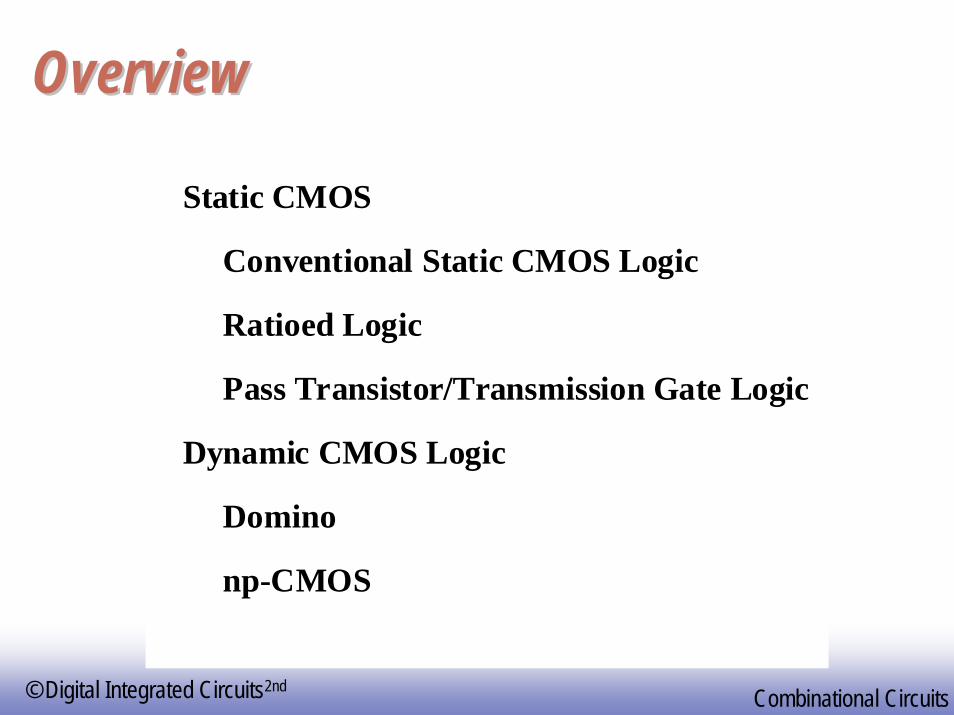
OverviewOverview
Static CMOS
Conventional Static CMOS Logic
Ratioed Logic
Pass Transistor/Transmission Gate Logic
Dynamic CMOS Logic
Domino
np-CMOS

EE1415
© Digital Integrated Circuits2nd Combinational Circuits
Combinational vs. Sequential LogicCombinational vs. Sequential Logic
Combinational Sequential
Output = f(In) Output = f(In, Previous In)
CombinationalLogicCircuit
OutInCombinational
LogicCircuit
OutIn
State
EE1416
© Digital Integrated Circuits2nd Combinational Circuits
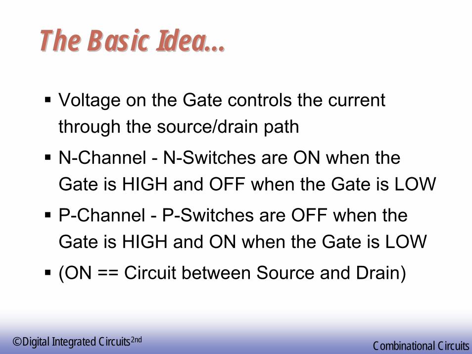
The Basic IdeaThe Basic Idea……
Voltage on the Gate controls the current through the source/drain path
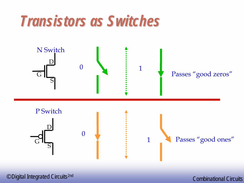
N-Channel - N-Switches are ON when the Gate is HIGH and OFF when the Gate is LOW
P-Channel - P-Switches are OFF when the Gate is HIGH and ON when the Gate is LOW
(ON == Circuit between Source and Drain)
EE1417
© Digital Integrated Circuits2nd Combinational Circuits
Transistors as SwitchesTransistors as Switches
GS
D
GS
D
N Switch
P Switch
0
1
1
0
Passes “good zeros”
Passes “good ones”

EE1418
© Digital Integrated Circuits2nd Combinational Circuits
…….The Rest of the Story....The Rest of the Story...
Put them in series - both must be on to complete the circuitPut them in parallel - either can be on to complete the circuit Generate all sorts of Switching Functions NOT the same as Boolean Functions.... Its RELAY logic - pin ball machines
EE1419
© Digital Integrated Circuits2nd Combinational Circuits
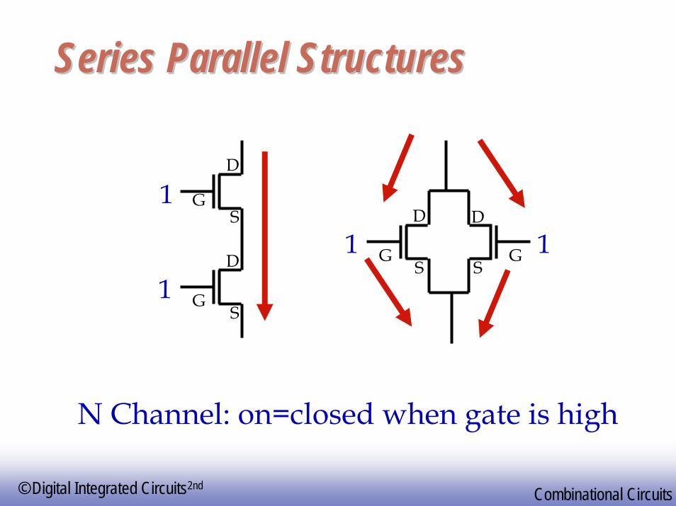
Series Parallel StructuresSeries Parallel Structures
N Channel: on=closed when gate is high
1
1
1 1
GS
D
GS
D G GS S
D D

EE14110
© Digital Integrated Circuits2nd Combinational Circuits
NMOS Transistors in Series/Parallel ConnectionNMOS Transistors in Series/Parallel Connection
Transistors can be thought as a switch controlled by its gate signal
NMOS switch closes when switch control input is high
X Y
A B
Y = X if A and B
X Y
A
B Y = X if A OR B
NMOS Transistors pass a “strong” 0 but a “weak” 1
Digital Integrated Circuits © Prentice Hall 1995IntroductionIntroduction

EE14111
© Digital Integrated Circuits2nd Combinational Circuits
Series Parallel Structures(2)Series Parallel Structures(2)
P Channel: on=closed when gate is low
0
0
0 0
GS
D
GS
D G GS S
D D
EE14112
© Digital Integrated Circuits2nd Combinational Circuits
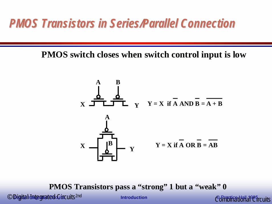
PMOS Transistors in Series/Parallel ConnectionPMOS Transistors in Series/Parallel Connection
X Y
A B
Y = X if A AND B = A + B
X Y
A
B Y = X if A OR B = AB
PMOS Transistors pass a “strong” 1 but a “weak” 0
PMOS switch closes when switch control input is low
Digital Integrated Circuits © Prentice Hall 1995IntroductionIntroduction

EE14113
© Digital Integrated Circuits2nd Combinational Circuits
……ThatThat’’s it!s it!
This is Non-Trivial: it defines the basis for the logic abstraction which is essential for all Boolean functions.
Provide a path to VDD for 1 Provide a path to GND for 0 For complex functions - provide complex paths

EE14114
© Digital Integrated Circuits2nd Combinational Circuits
From Switches to Boolean From Switches to Boolean Functions... Functions...
Use the Switching Functions to provide paths to Vdd or GND
Vdd is the source of all Truth (Vdd = = 1)GND is the source of all Falsehood (GND == 0)
P-channel N-channel
0
0
1
1
EE14115
© Digital Integrated Circuits2nd Combinational Circuits
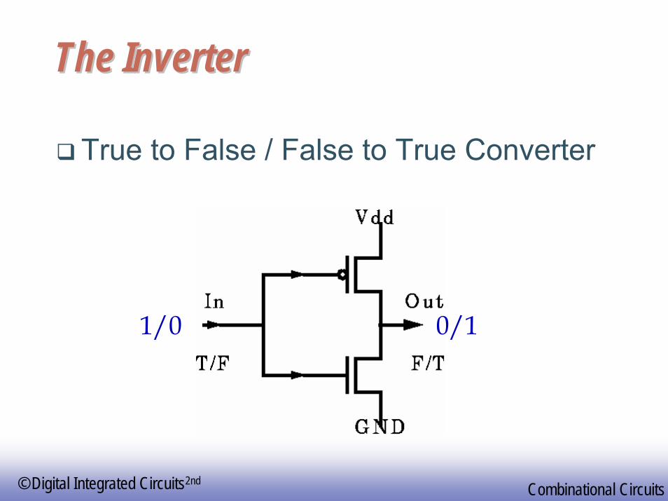
The Inverter The Inverter
True to False / False to True Converter
1/0 0/1
EE14116
© Digital Integrated Circuits2nd Combinational Circuits
Static CMOS CircuitStatic CMOS Circuit
At every point in time (except during the switching transients) each gate output is connected to eitherVDD or Vss via a low-resistive path.
The outputs of the gates assume at all times the value of the Boolean function, implemented by the circuit (ignoring, once again, the transient effects during switching periods).
This is in contrast to the dynamic circuit class, which relies on temporary storage of signal values on the capacitance of high impedance circuit nodes.
EE14117
© Digital Integrated Circuits2nd Combinational Circuits
The ExceptionsThe Exceptions
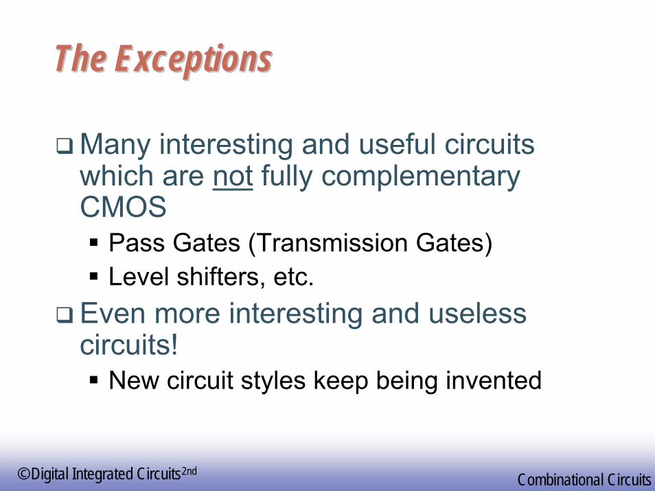
Many interesting and useful circuits which are not fully complementary CMOS
Pass Gates (Transmission Gates)Level shifters, etc.
Even more interesting and useless circuits!
New circuit styles keep being invented

EE14118
© Digital Integrated Circuits2nd Combinational Circuits
Threshold DropsThreshold DropsVDD
VDD → 0PDN
0 → VDD
CL
CL
PUN
VDD
0 → VDD - VTn
CL
VDD
VDD
VDD → |VTp|
CL
S
D S
D
VGS
S
SD
D
VGS

EE14119
© Digital Integrated Circuits2nd Combinational Circuits
Series Parallel Structures (3)Series Parallel Structures (3)
GS D
GSD
N Switch
P Switch
0
1
1
0
Passes “good zeros”
Passes “good ones”
Bi-directional SwitchOpen Circuit, High Z
S
S’
EE14120
© Digital Integrated Circuits2nd Combinational Circuits
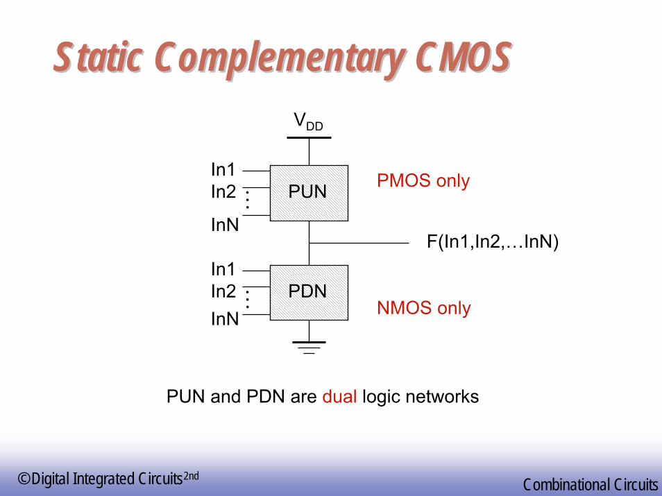
Static Complementary CMOSStatic Complementary CMOSVDD
F(In1,In2,…InN)
In1In2
InN
In1In2InN
PUN
PDN
……
PMOS only
NMOS only
PUN and PDN are dual logic networks

EE14121
© Digital Integrated Circuits2nd Combinational Circuits
Complementary CMOS Logic StyleComplementary CMOS Logic Style

EE14122
© Digital Integrated Circuits2nd Combinational Circuits
Example Gate: NANDExample Gate: NAND
EE14123
© Digital Integrated Circuits2nd Combinational Circuits
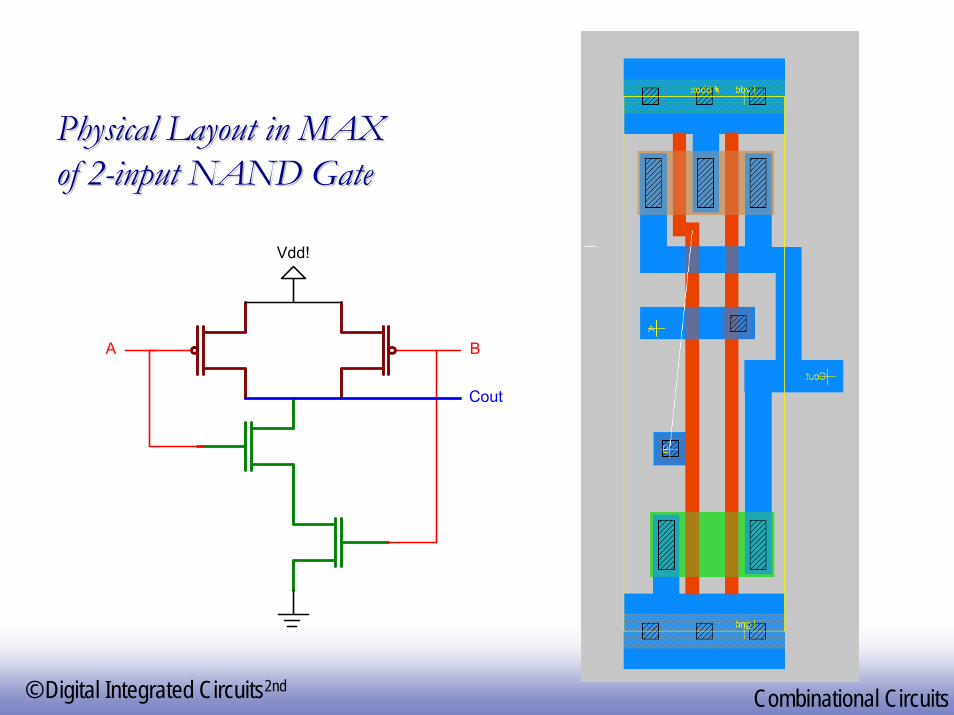
Physical Layout in MAXPhysical Layout in MAXof 2of 2--input NAND Gateinput NAND Gate
Vdd!
A B
Cout

EE14124
© Digital Integrated Circuits2nd Combinational Circuits
44--input NAND Gateinput NAND Gate
In3
In1
In2
In4
In1 In2 In3 In4
VDD
Out
In1 In2 In3 In4
Vdd
GND
Out
Digital Integrated Circuits © Prentice Hall 1995IntroductionIntroduction

EE14125
© Digital Integrated Circuits2nd Combinational Circuits
Example Gate: NORExample Gate: NOR

EE14126
© Digital Integrated Circuits2nd Combinational Circuits
Physical Layout in MAXPhysical Layout in MAXof 2of 2--input NOR Gateinput NOR Gate

EE14127
© Digital Integrated Circuits2nd Combinational Circuits
Constructing a Complex GateConstructing a Complex Gate
C
(a) pull-down network
SN1 SN4
SN2
SN3D
FF
A
DB
C
D
F
A
B
C
(b) Deriving the pull-up networkhierarchically by identifyingsub-nets
D
A
A
B
C
VDD VDD
B
(c) complete gate
EE14128
© Digital Integrated Circuits2nd Combinational Circuits
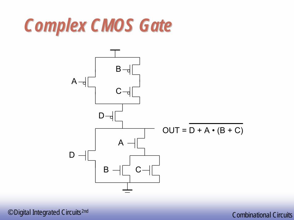
Complex CMOS GateComplex CMOS Gate
OUT = D + A • (B + C)
DA
B C
D
AB
C
EE14129
© Digital Integrated Circuits2nd Combinational Circuits
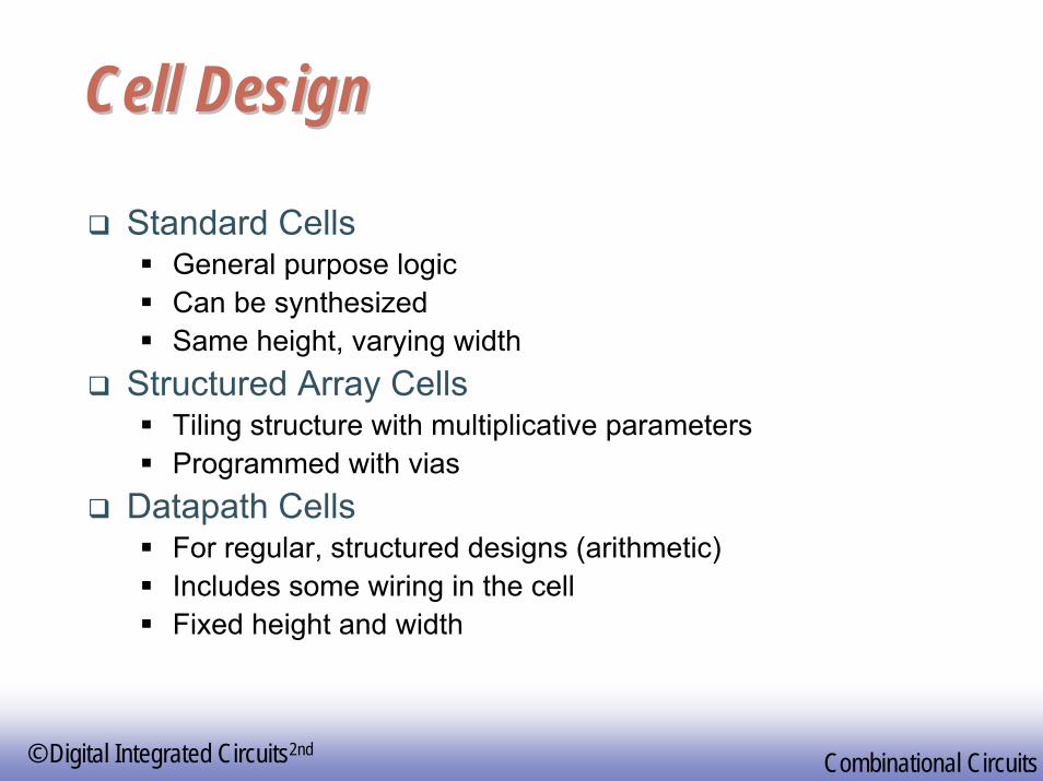
Cell DesignCell Design
Standard CellsGeneral purpose logicCan be synthesizedSame height, varying width
Structured Array CellsTiling structure with multiplicative parametersProgrammed with vias
Datapath CellsFor regular, structured designs (arithmetic)Includes some wiring in the cellFixed height and width
EE14130
© Digital Integrated Circuits2nd Combinational Circuits
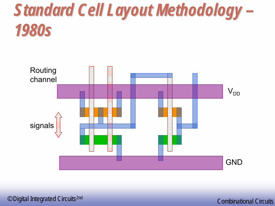
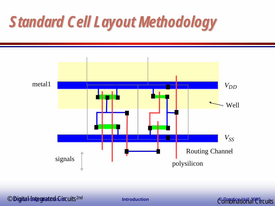
Standard Cell Layout Methodology Standard Cell Layout Methodology ––1980s1980s
signals
Routingchannel
VDD
GND
EE14131
© Digital Integrated Circuits2nd Combinational Circuits
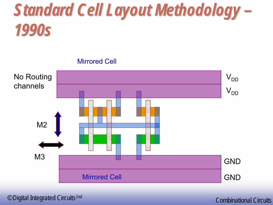
Standard Cell Layout Methodology Standard Cell Layout Methodology ––1990s1990s
M2
No Routingchannels VDD
GNDM3
VDD
GND
Mirrored Cell
Mirrored Cell
EE14132
© Digital Integrated Circuits2nd Combinational Circuits
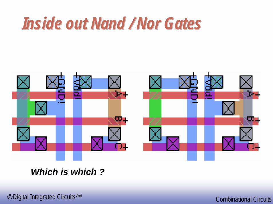
Inside out Inside out NandNand / Nor Gates / Nor Gates
Which is which ?
EE14133
© Digital Integrated Circuits2nd Combinational Circuits
Standard Cell Layout MethodologyStandard Cell Layout Methodology
VDD
VSS
Well
signalsRouting Channel
metal1
polysilicon
Digital Integrated Circuits © Prentice Hall 1995IntroductionIntroduction

EE14134
© Digital Integrated Circuits2nd Combinational Circuits
Standard CellsStandard Cells
Cell boundary
N WellCell height 12 metal tracksMetal track is approx. 3λ + 3λPitch = repetitive distance between objects
Cell height is “12 pitch”
2λ
Rails ~10λ
InOut
VDD
GND

EE14135
© Digital Integrated Circuits2nd Combinational Circuits
Standard CellsStandard Cells
InOut
VDD
GND
In Out
VDD
GND
With silicideddiffusion
With minimaldiffusionrouting
OutIn
VDD
M2
M1

EE14136
© Digital Integrated Circuits2nd Combinational Circuits
Standard CellsStandard Cells
A
Out
VDD
GND
B
2-input NAND gate
B
VDD
A
Note: well and substrate Contactsprevent external routing in poly

EE14137
© Digital Integrated Circuits2nd Combinational Circuits
MultiMulti--Fingered TransistorsFingered TransistorsOne finger Two fingers (folded)
Less diffusion capacitance

EE14138
© Digital Integrated Circuits2nd Combinational Circuits
Stick DiagramsStick Diagrams
Contains no dimensionsRepresents relative positions of transistors
In
Out
VDD
GND
Inverter
A
Out
VDD
GNDB
NAND2

EE14139
© Digital Integrated Circuits2nd Combinational Circuits
Stick DiagramsStick Diagrams
C
A B
X = C • (A + B)
B
AC
i
j
j
VDDX
X
i
GND
AB
C
PUN
PDNABC
Logic Graph
EE14140
© Digital Integrated Circuits2nd Combinational Circuits
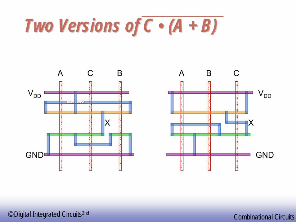
Two Versions of C Two Versions of C •• (A + B)(A + B)
X
CA B A B C
X
VDD
GND
VDD
GND
EE14141
© Digital Integrated Circuits2nd Combinational Circuits
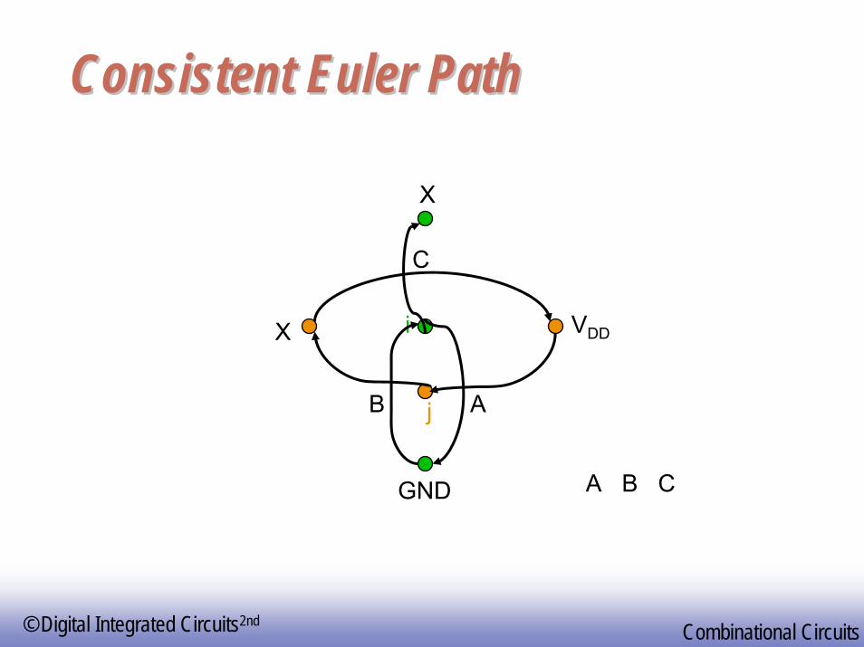
Consistent Euler PathConsistent Euler Path
j
VDDX
X
i
AB
C
GND A B C
EE14142
© Digital Integrated Circuits2nd Combinational Circuits
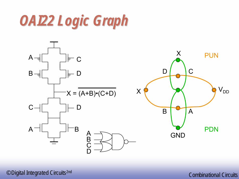
OAI22 Logic GraphOAI22 Logic Graph
C
A B
X = (A+B)•(C+D)
B
A
D
VDDX
X
AB
GND
C
PUN
PDN
C
D
D
ABCD
EE14143
© Digital Integrated Circuits2nd Combinational Circuits
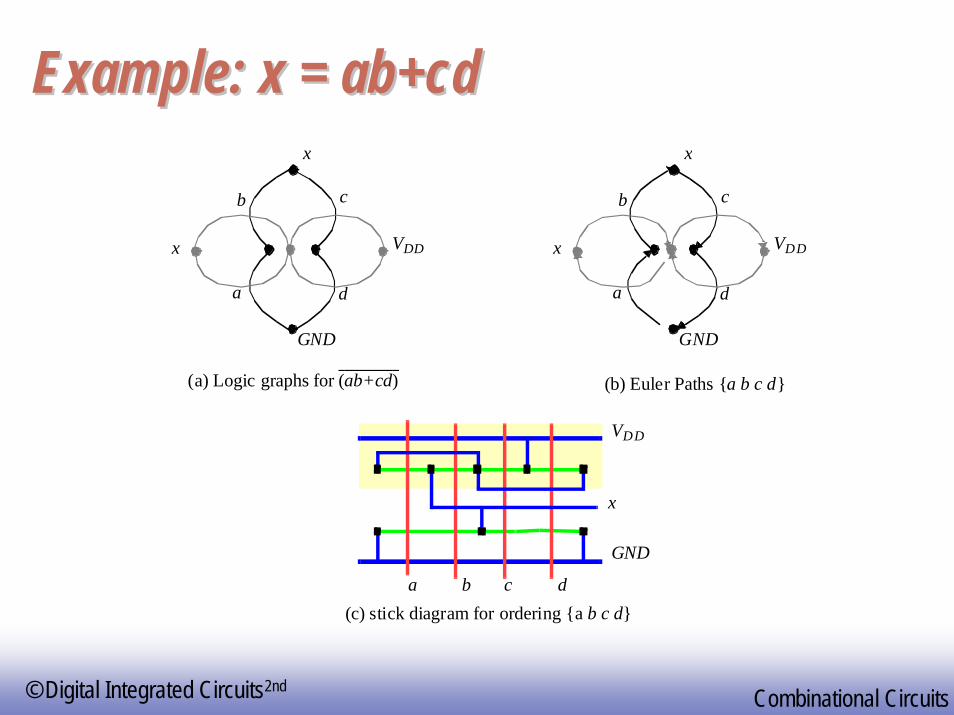
Example: x = Example: x = ab+cdab+cd
GND
x
a
b c
d
VDDx
GND
x
a
b c
d
VDDx
(a) Logic graphs for (ab+cd) (b) Euler Paths {a b c d}
a c d
x
VDD
GND
(c) stick diagram for ordering {a b c d}b
EE14144
© Digital Integrated Circuits2nd Combinational Circuits
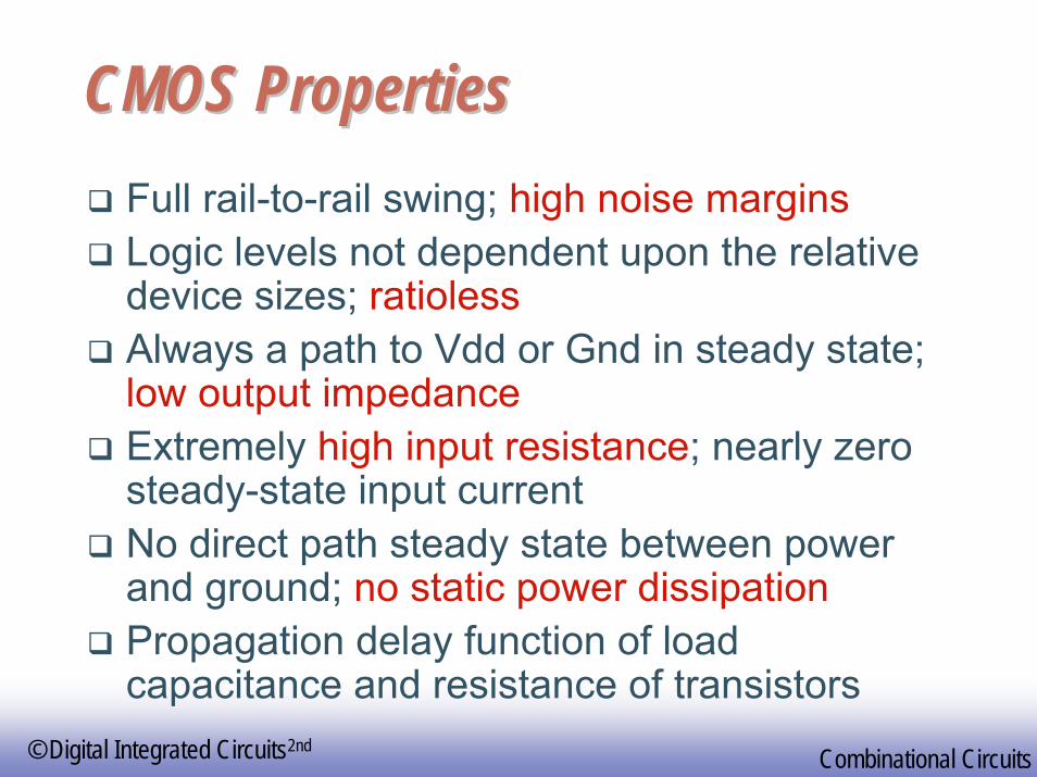
CMOS PropertiesCMOS PropertiesFull rail-to-rail swing; high noise marginsLogic levels not dependent upon the relative device sizes; ratiolessAlways a path to Vdd or Gnd in steady state; low output impedanceExtremely high input resistance; nearly zero steady-state input currentNo direct path steady state between power and ground; no static power dissipationPropagation delay function of load capacitance and resistance of transistors

EE14145
© Digital Integrated Circuits2nd Combinational Circuits
Complex Gate StructuresComplex Gate Structures
A
C
B
A
B
Vdd
Gnd
Out
C
Out = A+(B*C) ...
ABC
And-Or-Invert (AOI)
How to add terms?
EE14146
© Digital Integrated Circuits2nd Combinational Circuits
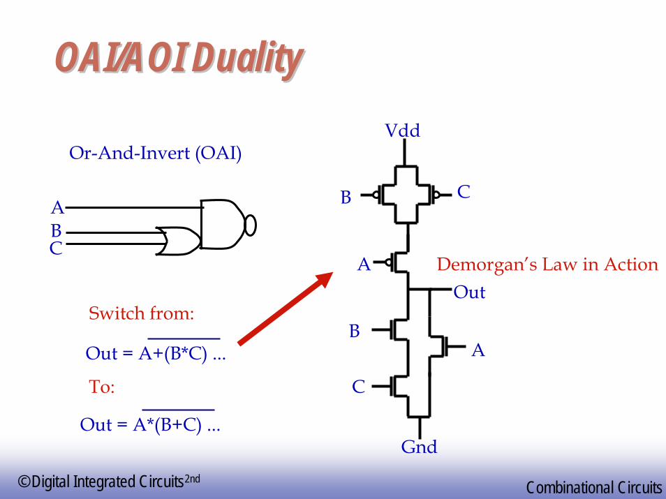
OAI/AOI DualityOAI/AOI Duality
A
C
B
A
B C
Vdd
Gnd
Out
Out = A*(B+C) ...
ABC
Out = A+(B*C) ...
Or-And-Invert (OAI)
Switch from:
To:
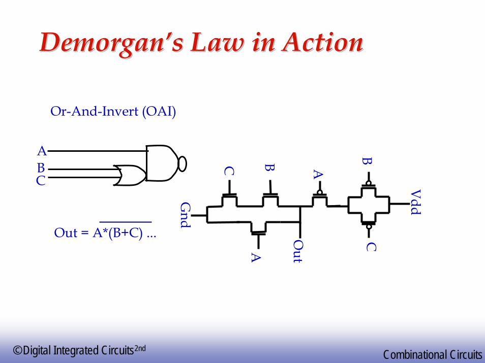
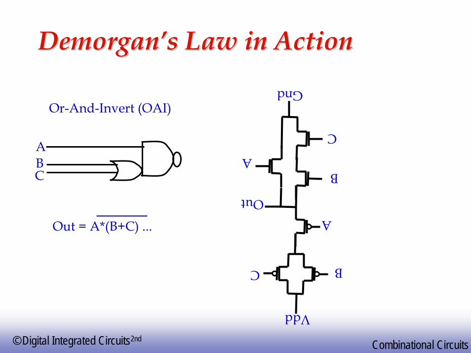
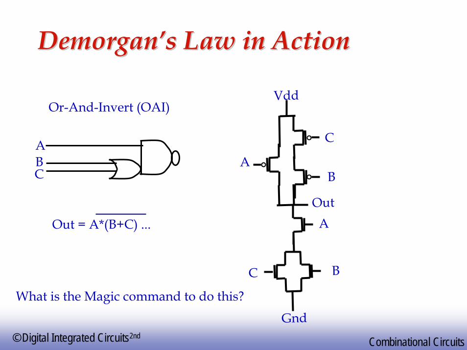
Demorgan’s Law in Action

EE14147
© Digital Integrated Circuits2nd Combinational Circuits
DemorganDemorgan’’ss Law in ActionLaw in Action
Out = A*(B+C) ...
ABC
Or-And-Invert (OAI)
A
C
B
A
B
C
Vdd
Gnd
Out
EE14148
© Digital Integrated Circuits2nd Combinational Circuits
DemorganDemorgan’’ss Law in ActionLaw in Action
Out = A*(B+C) ...
ABC
Or-And-Invert (OAI)
A
C B A
BC
Vd dG
n d
Ou t

EE14149
© Digital Integrated Circuits2nd Combinational Circuits
DemorganDemorgan’’ss Law in ActionLaw in Action
Out = A*(B+C) ...
ABC
Or-And-Invert (OAI)
A
C
B
A
B
C
Vdd
Gnd
Out
EE14150
© Digital Integrated Circuits2nd Combinational Circuits
DemorganDemorgan’’ss Law in ActionLaw in Action
Out = A*(B+C) ...
ABC
Or-And-Invert (OAI)
A
C
B
A
BC
Vdd
Gnd
Out
EE14151
© Digital Integrated Circuits2nd Combinational Circuits
DemorganDemorgan’’ss Law in ActionLaw in Action
Out = A*(B+C) ...
ABC
Or-And-Invert (OAI)
A
Vdd
Gnd
Out
C
B
A
BC
What is the Magic command to do this?

EE14152
© Digital Integrated Circuits2nd Combinational Circuits
Complex (AOI/OAI) GatesComplex (AOI/OAI) Gates

EE14153
© Digital Integrated Circuits2nd Combinational Circuits
Schematic Representation in SUESchematic Representation in SUEof AOI (andof AOI (and--oror--invert) Gateinvert) Gate
Notice 6 transistors

EE14154
© Digital Integrated Circuits2nd Combinational Circuits
Physical Layout in MAX of AOI GatePhysical Layout in MAX of AOI Gate
A
OUT
Vdd!
A
B
BC
C
B
A
C
OUT

EE14155
© Digital Integrated Circuits2nd Combinational Circuits
Schematic Representation in SUESchematic Representation in SUEof OAI (orof OAI (or--andand--invert)invert)
EE14156
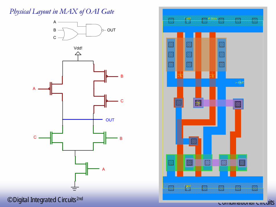
© Digital Integrated Circuits2nd Combinational Circuits
Physical Layout in MAX of OAI GatePhysical Layout in MAX of OAI Gate
A
OUT
Vdd!
A
B
B
C
C
A
B
C
OUT
EE14157
© Digital Integrated Circuits2nd Combinational Circuits
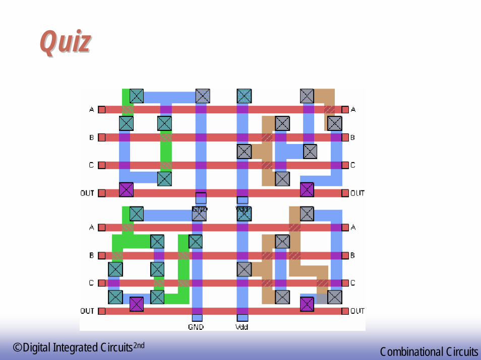
QuizQuiz

EE14158
© Digital Integrated Circuits2nd Combinational Circuits
Step by Step Layout of XNOR Gate Step by Step Layout of XNOR Gate
– The equation for XNOR is: f = (a * b) + (a' * b')
– using DeMorgan's law on each of the two terms gives:f = (a'+ b')' + (a + b)'
– using DeMorgan's law on the two terms together gives:
f = ((a'+ b') * (a + b))'
– This could be directly implemented with a single complementary CMOS gate: the equation is in a simple negated product of sums form. This form can be implemented with the standard Or-And-Invert (OAI) style gate.
EE14159
© Digital Integrated Circuits2nd Combinational Circuits
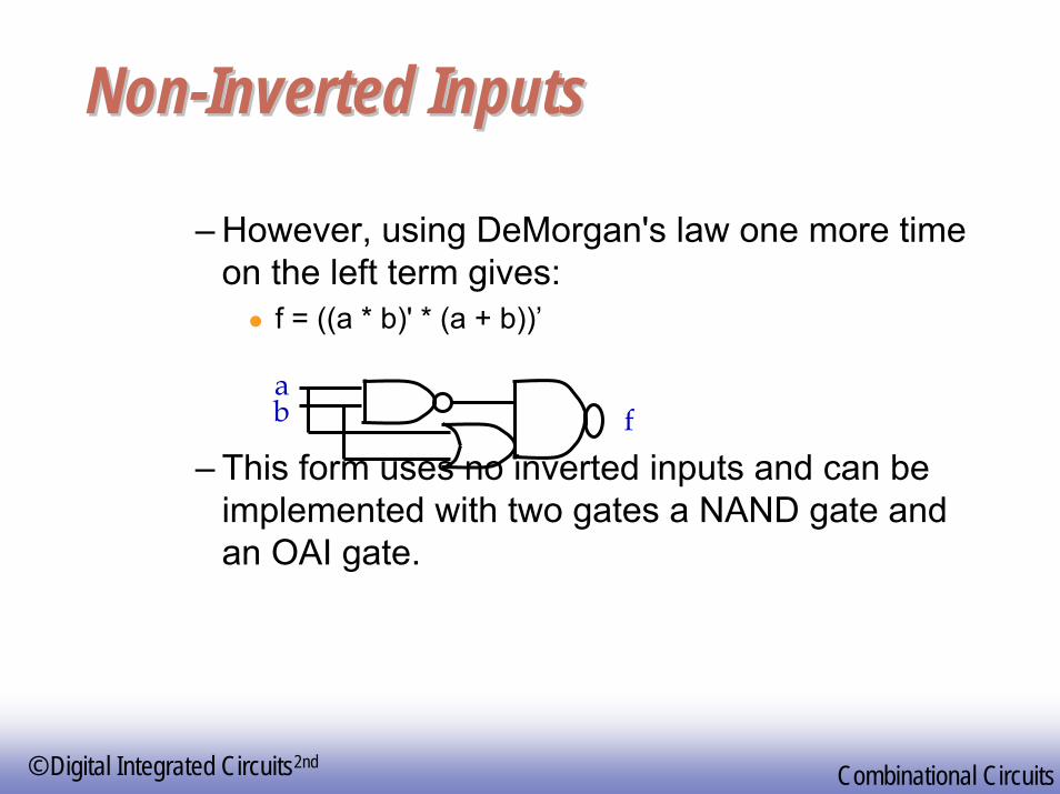
NonNon--Inverted InputsInverted Inputs
– However, using DeMorgan's law one more time on the left term gives:
f = ((a * b)' * (a + b))’
– This form uses no inverted inputs and can be implemented with two gates a NAND gate and an OAI gate.
ab f

EE14160
© Digital Integrated Circuits2nd Combinational Circuits
Now lets lay it outNow lets lay it out
Start with Vdd! and GND! power buses. Without any more information, about the use of this cell, make the power and ground lines in metal 1sized 3 and 3 apart. Use poly as inputs A B and guess that C might be used.

EE14161
© Digital Integrated Circuits2nd Combinational Circuits
XOR from NOR/AOIXOR from NOR/AOI

EE14162
© Digital Integrated Circuits2nd Combinational Circuits
EE14163
© Digital Integrated Circuits2nd Combinational Circuits
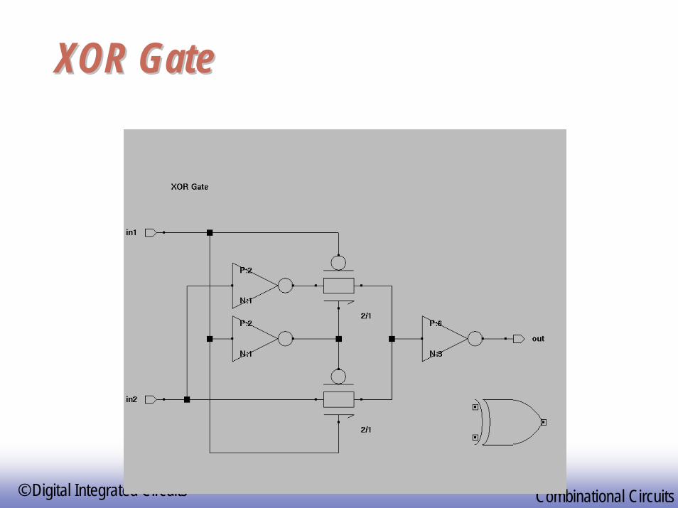
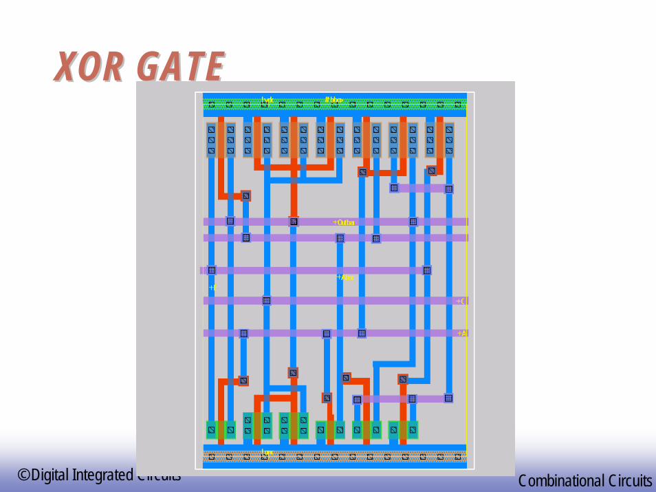
XOR GateXOR Gate

EE14164
© Digital Integrated Circuits2nd Combinational Circuits
IrsimIrsim
EE14165
© Digital Integrated Circuits2nd Combinational Circuits
XOR GATEXOR GATE

EE14166
© Digital Integrated Circuits2nd Combinational Circuits
3.5um x 10um3.5um x 10um

EE14167
© Digital Integrated Circuits2nd Combinational Circuits
.35um x 1um.35um x 1um
EE14168
© Digital Integrated Circuits2nd Combinational Circuits
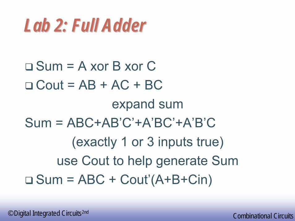
Lab 2: Full AdderLab 2: Full Adder
Sum = A xor B xor CCout = AB + AC + BC
expand sumSum = ABC+AB’C’+A’BC’+A’B’C
(exactly 1 or 3 inputs true)use Cout to help generate Sum
Sum = ABC + Cout’(A+B+Cin)
EE14169
© Digital Integrated Circuits2nd Combinational Circuits
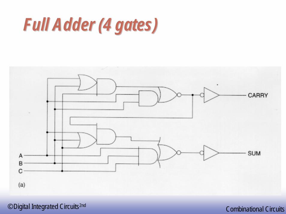
Full Adder (4 gates)Full Adder (4 gates)
EE14170
© Digital Integrated Circuits2nd Combinational Circuits
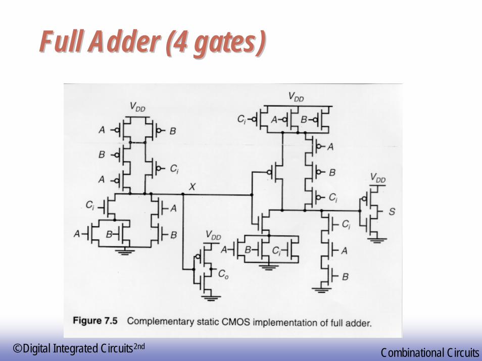
Full Adder (4 gates)Full Adder (4 gates)

EE14171
© Digital Integrated Circuits2nd Combinational Circuits

EE14172
© Digital Integrated Circuits2nd Combinational Circuits

EE14173
© Digital Integrated Circuits2nd Combinational Circuits

EE14174
© Digital Integrated Circuits2nd Combinational Circuits
One Solution (125x136)One Solution (125x136)
EE14175
© Digital Integrated Circuits2nd Combinational Circuits
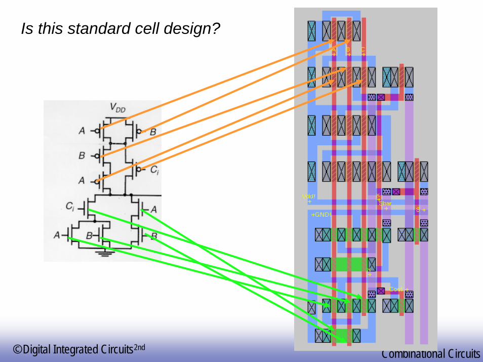
Is this standard cell design?

EE14176
© Digital Integrated Circuits2nd Combinational Circuits
Lab 3: 8 Bit Ripple Carry AdderLab 3: 8 Bit Ripple Carry Adder

EE14177
© Digital Integrated Circuits2nd Combinational Circuits
XX--pandedpanded
EE14178
© Digital Integrated Circuits2nd Combinational Circuits
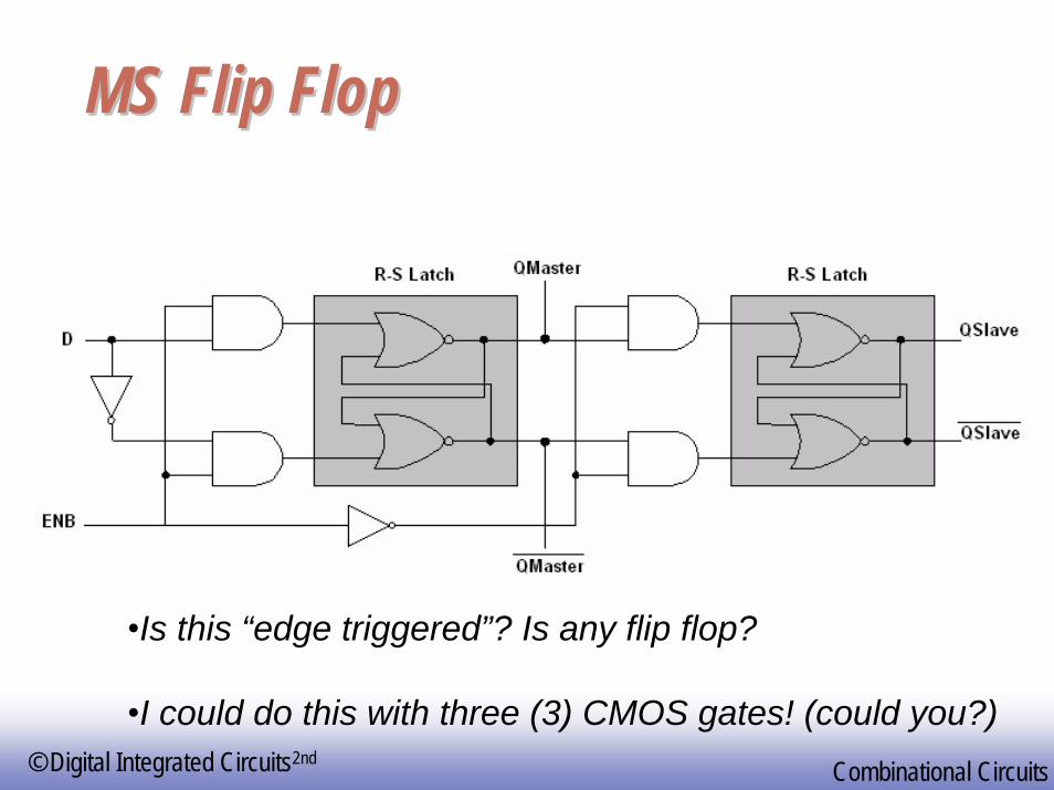
MS Flip FlopMS Flip Flop
•Is this “edge triggered”? Is any flip flop?
•I could do this with three (3) CMOS gates! (could you?)
EE14179
© Digital Integrated Circuits2nd Combinational Circuits
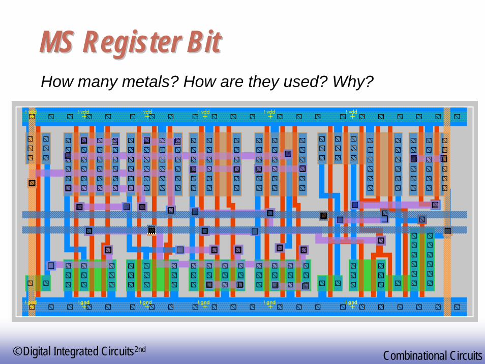
MS Register BitMS Register BitHow many metals? How are they used? Why?
EE14180
© Digital Integrated Circuits2nd Combinational Circuits
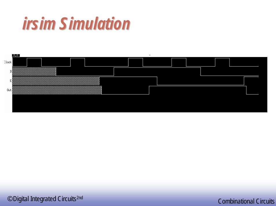
irsimirsim SimulationSimulation
EE14181
© Digital Integrated Circuits2nd Combinational Circuits
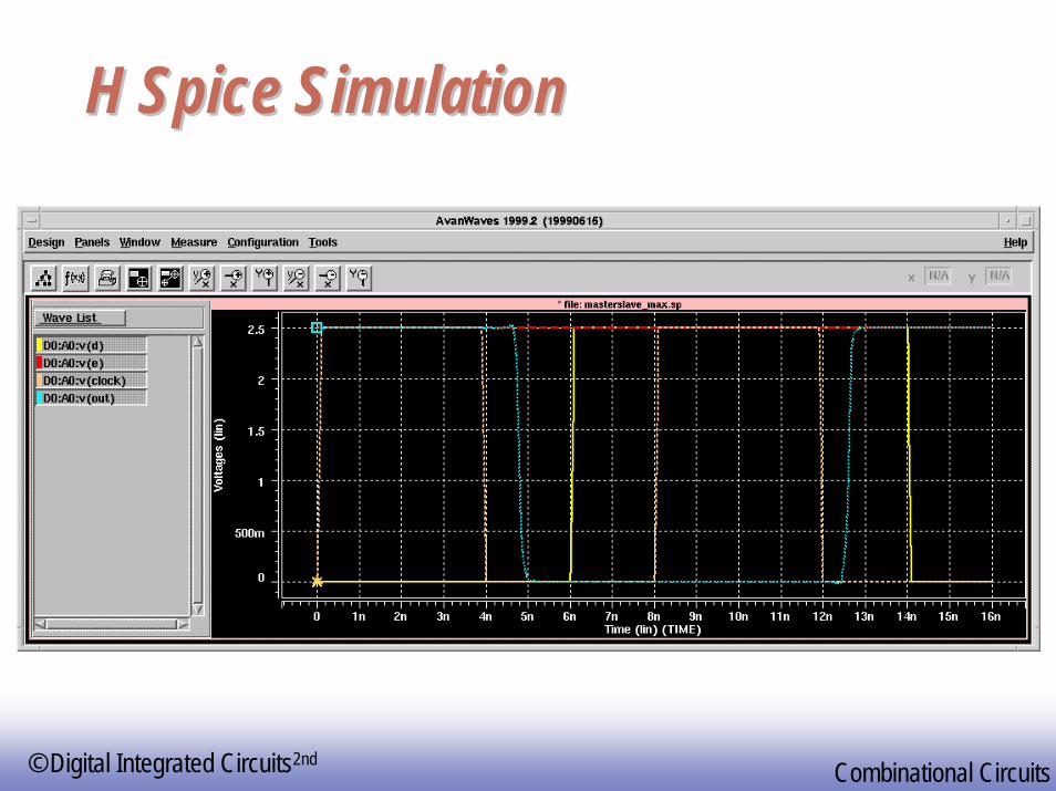
H Spice SimulationH Spice Simulation
EE14182
© Digital Integrated Circuits2nd Combinational Circuits
EE14183
© Digital Integrated Circuits2nd Combinational Circuits
EE14184
© Digital Integrated Circuits2nd Combinational Circuits
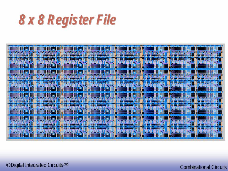
8 x 8 Register File8 x 8 Register File

EE14185
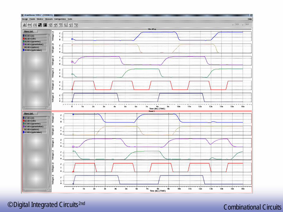
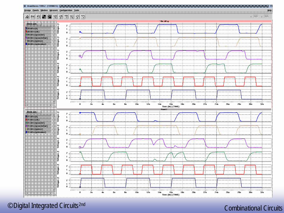
© Digital Integrated Circuits2nd Combinational Circuits
Register file simulation Register file simulation

EE14186
© Digital Integrated Circuits2nd Combinational Circuits
Properties of Complementary CMOS Gates Properties of Complementary CMOS Gates SnapshotSnapshot
High noise margins: VOH and VOL are at VDD and GND, respectively.
No static power consumption:There never exists a direct path between VDD and VSS (GND) in steady-state mode.
Comparable rise and fall times:(under appropriate sizing conditions)

EE14187
© Digital Integrated Circuits2nd Combinational Circuits
Switch Delay ModelSwitch Delay Model
A
Req
A
Rp
A
Rp
A
Rn CL
A
CL
B
Rn
A
Rp
B
Rp
A
Rn Cint
B
Rp
A
Rp
A
Rn
B
Rn CL
Cint
NAND2 INV NOR2

EE14188
© Digital Integrated Circuits2nd Combinational Circuits
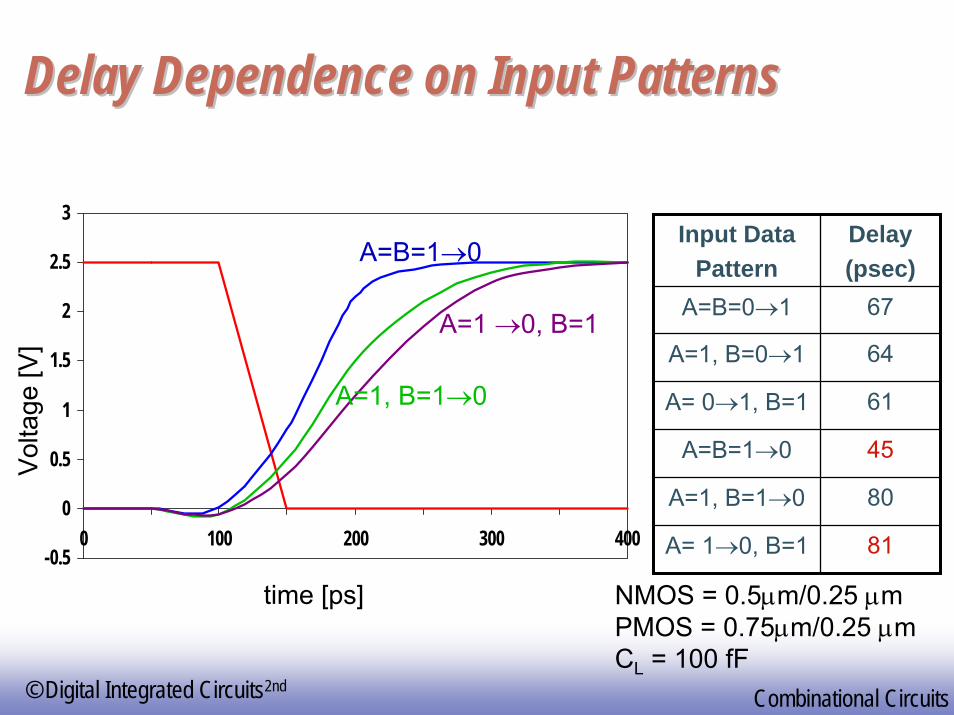
Input Pattern Effects on DelayInput Pattern Effects on Delay
Delay is dependent on the pattern of inputsLow to high transition
both inputs go low– delay is 0.69 Rp/2 CL
one input goes low– delay is 0.69 Rp CL
High to low transitionboth inputs go high
– delay is 0.69 2Rn CL
CL
B
Rn
ARp
BRp
A
Rn Cint
EE14189
© Digital Integrated Circuits2nd Combinational Circuits
Delay Dependence on Input PatternsDelay Dependence on Input Patterns
-0.5
0
0.5
1
1.5
2
2.5
3
0 100 200 300 400
A=B=1→0
A=1, B=1→0
A=1 →0, B=1
time [ps]
Vol
tage
[V]
Input DataPattern
Delay(psec)
A=B=0→1 67
A=1, B=0→1 64
A= 0→1, B=1 61
A=B=1→0 45
A=1, B=1→0 80
A= 1→0, B=1 81
NMOS = 0.5μm/0.25 μmPMOS = 0.75μm/0.25 μmCL = 100 fF

EE14190
© Digital Integrated Circuits2nd Combinational Circuits
Transistor SizingTransistor Sizing
CL
B
Rn
A
Rp
B
Rp
A
Rn Cint
B
Rp
A
Rp
A
Rn
B
Rn CL
Cint
2
2
2 2
11
4
4
EE14191
© Digital Integrated Circuits2nd Combinational Circuits
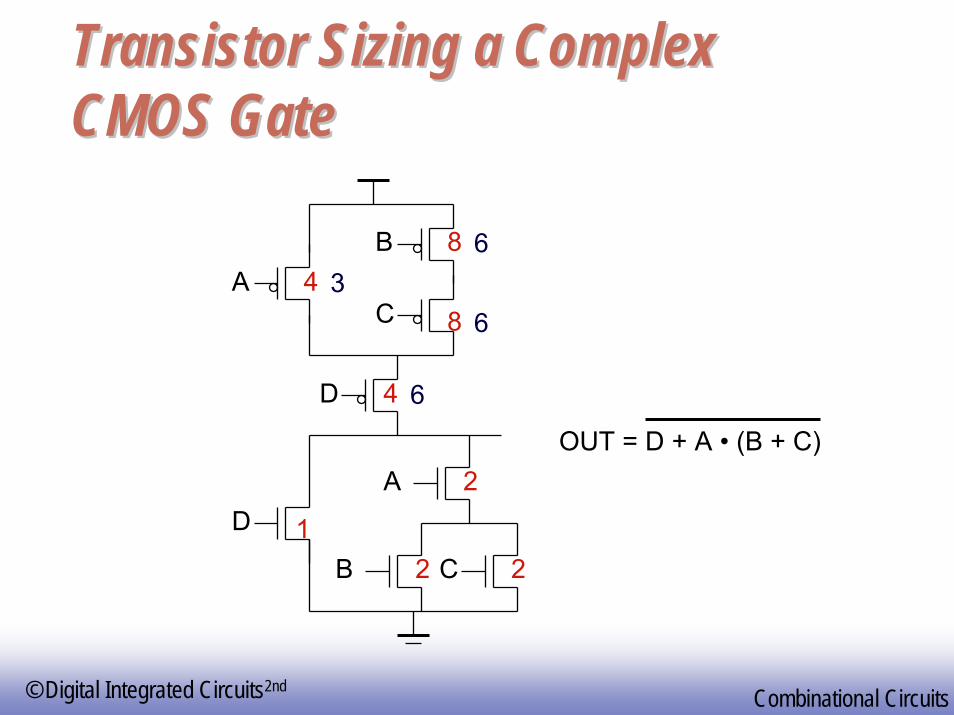
Transistor Sizing a Complex Transistor Sizing a Complex CMOS GateCMOS Gate
OUT = D + A • (B + C)
DA
B C
D
AB
C
1
2
2 2
4
48
8
6
36
6

EE14192
© Digital Integrated Circuits2nd Combinational Circuits
FanFan--In ConsiderationsIn Considerations
DCBA
D
C
B
A CL
C3
C2
C1
Distributed RC model(Elmore delay)
tpHL = 0.69 Reqn(C1+2C2+3C3+4CL)
Propagation delay deteriorates rapidly as a function of fan-in –quadratically in the worst case.

EE14193
© Digital Integrated Circuits2nd Combinational Circuits
ttpp as a Function of Fanas a Function of Fan--InIn
tpLH
t p(p
sec)
fan-in
Gates with a fan-in greater than 4 should be avoided.
0
250
500
750
1000
1250
2 4 6 8 10 12 14 16
tpHL
quadratic
linear
tp

EE14194
© Digital Integrated Circuits2nd Combinational Circuits
ttpp as a Function of Fanas a Function of Fan--OutOut
2 4 6 8 10 12 14 16
tpNOR2
t p(p
sec)
eff. fan-out
tpNAND2
tpINV
All gates have the same drive current.
Slope is a function of “driving strength”
EE14195
© Digital Integrated Circuits2nd Combinational Circuits
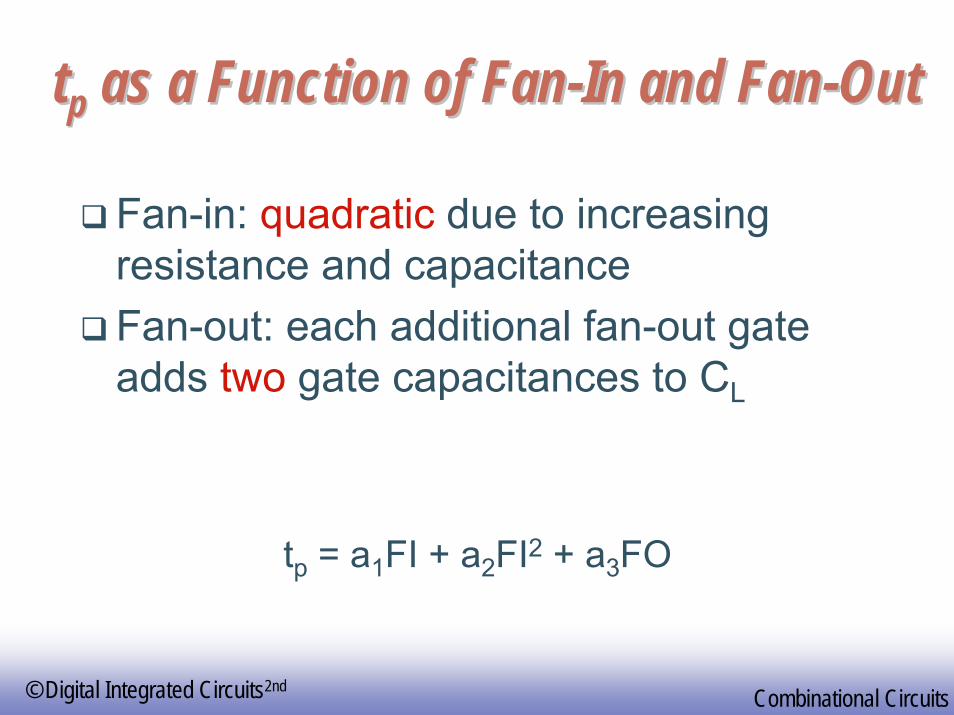
ttpp as a Function of Fanas a Function of Fan--In and FanIn and Fan--OutOut
Fan-in: quadratic due to increasing resistance and capacitanceFan-out: each additional fan-out gate adds two gate capacitances to CL
tp = a1FI + a2FI2 + a3FO
EE14196
© Digital Integrated Circuits2nd Combinational Circuits
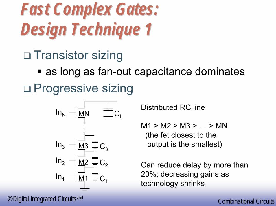
Fast Complex Gates:Fast Complex Gates:Design Technique 1Design Technique 1
Transistor sizingas long as fan-out capacitance dominates
Progressive sizing
InN CL
C3
C2
C1In1
In2
In3
M1
M2
M3
MNDistributed RC line
M1 > M2 > M3 > … > MN(the fet closest to theoutput is the smallest)
Can reduce delay by more than 20%; decreasing gains as technology shrinks
EE14197
© Digital Integrated Circuits2nd Combinational Circuits
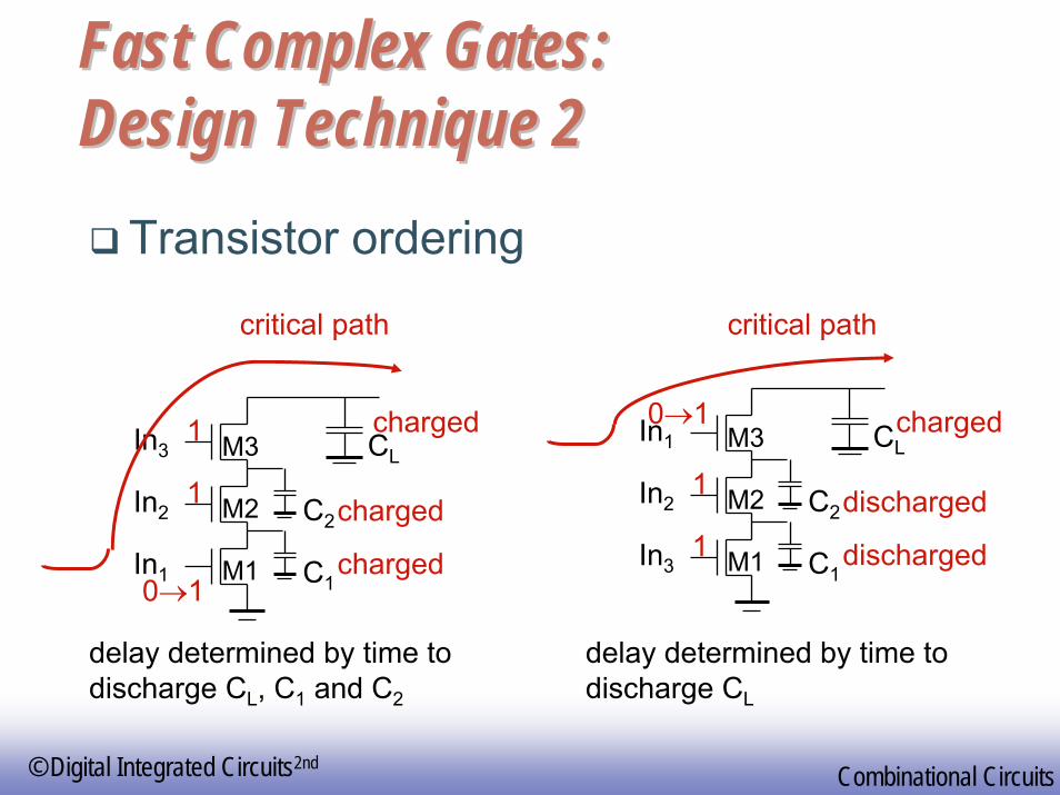
Fast Complex Gates:Fast Complex Gates:Design Technique 2Design Technique 2
Transistor ordering
C2
C1In1
In2
In3
M1
M2
M3 CL
C2
C1In3
In2
In1
M1
M2
M3 CL
critical path critical path
charged1
0→1charged
charged1
delay determined by time to discharge CL, C1 and C2
delay determined by time to discharge CL
1
1
0→1 charged
discharged
discharged

EE14198
© Digital Integrated Circuits2nd Combinational Circuits
Fast Complex Gates:Fast Complex Gates:Design Technique 3Design Technique 3Alternative logic structures
F = ABCDEFGH
EE14199
© Digital Integrated Circuits2nd Combinational Circuits
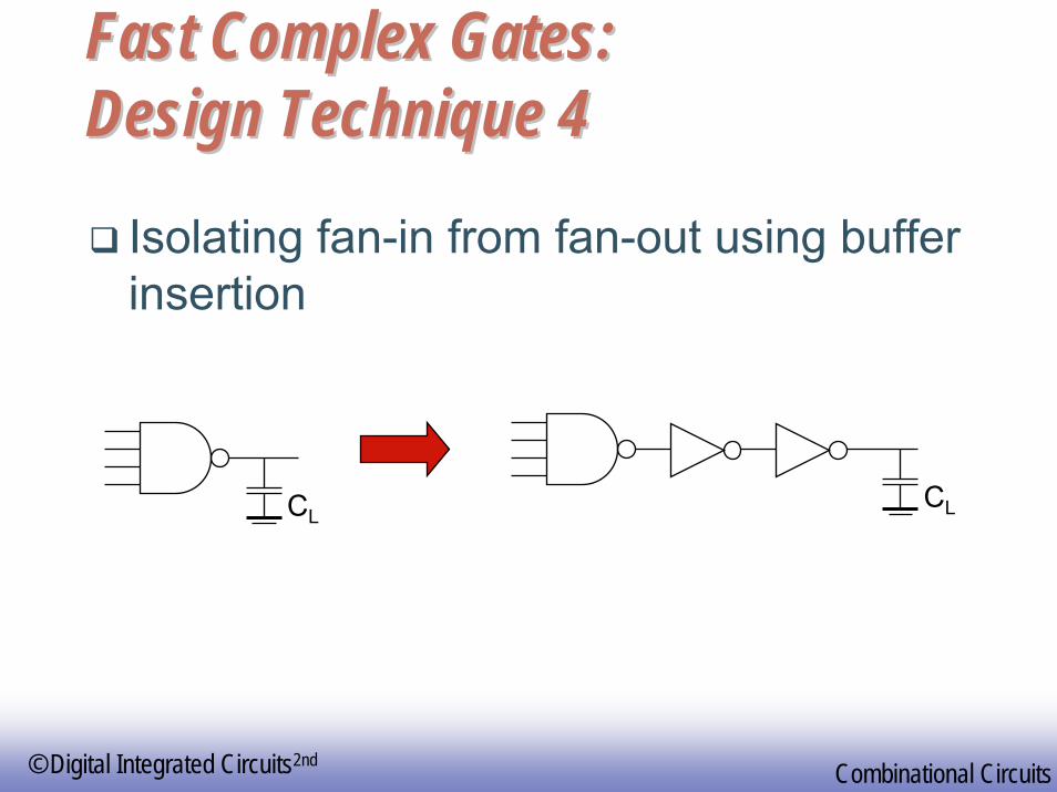
Fast Complex Gates:Fast Complex Gates:Design Technique 4Design Technique 4
Isolating fan-in from fan-out using buffer insertion
CLCL

EE141100
© Digital Integrated Circuits2nd Combinational Circuits
Fast Complex Gates:Fast Complex Gates:Design Technique 5Design Technique 5
Reducing the voltage swing
linear reduction in delayalso reduces power consumption
But the following gate is much slower!Or requires use of “sense amplifiers” on the receiving end to restore the signal level (memory design)
tpHL = 0.69 (3/4 (CL VDD)/ IDSATn )
= 0.69 (3/4 (CL Vswing)/ IDSATn )

EE141101
© Digital Integrated Circuits2nd Combinational Circuits
Sizing Logic Paths for SpeedSizing Logic Paths for Speed
Frequently, input capacitance of a logic path is constrainedLogic also has to drive some capacitanceExample: ALU load in an Intel’s microprocessor is 0.5pFHow do we size the ALU datapath to achieve maximum speed?We have already solved this for the inverter chain – can we generalize it for any type of logic?

EE141102
© Digital Integrated Circuits2nd Combinational Circuits
Buffer ExampleBuffer Example
( )∑=
⋅+=N
iiii fgpDelay
1
Out
For given N: Ci+1/Ci = Ci/Ci-1To find N: Ci+1/Ci ~ 4How to generalize this to any logic path?
CL
In
1 2 N
(in units of τinv)

EE141103
© Digital Integrated Circuits2nd Combinational Circuits
Logical EffortLogical Effort
( )fgpCCCRkDelay
in
Lunitunit
⋅+=
⎟⎟⎠
⎞⎜⎜⎝
⎛+⋅=
τγ
1
p – intrinsic delay (3kRunitCunitγ) - gate parameter ≠ f(W)g – logical effort (kRunitCunit) – gate parameter ≠ f(W)f – effective fanout
Normalize everything to an inverter:ginv =1, pinv = 1
Divide everything by τinv(everything is measured in unit delays τinv)Assume γ = 1.
EE141104
© Digital Integrated Circuits2nd Combinational Circuits
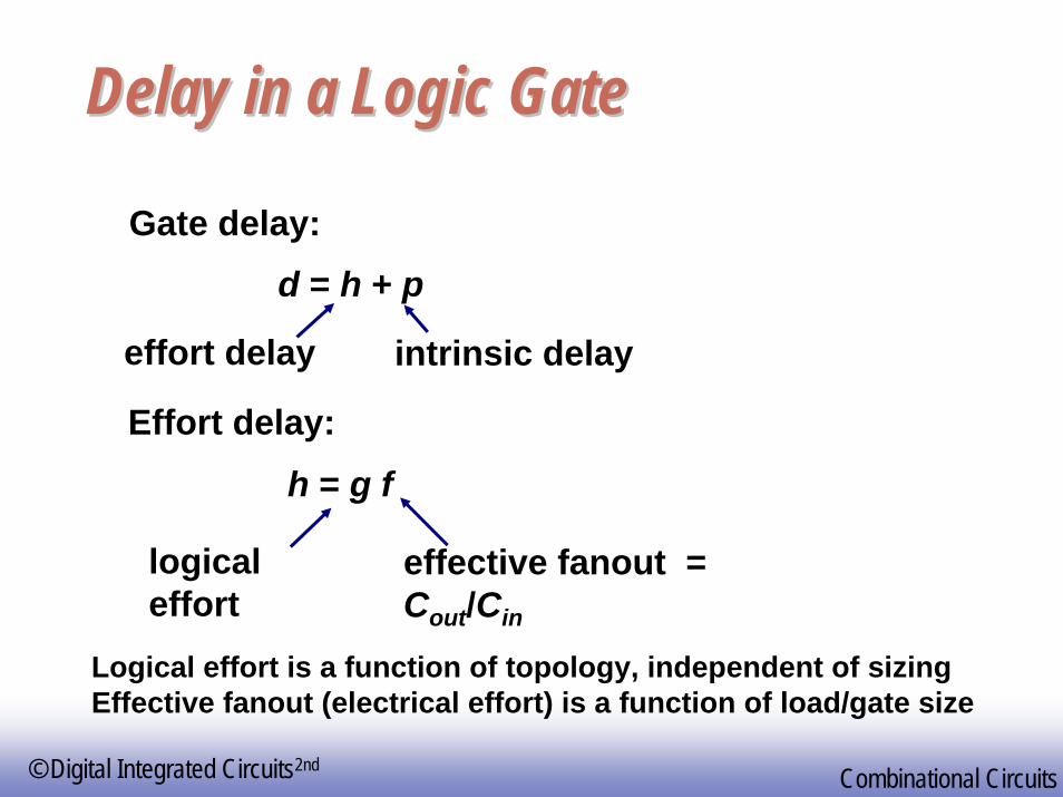
Delay in a Logic GateDelay in a Logic Gate
Gate delay:d = h + p
effort delay intrinsic delay
Effort delay:
h = g f
effective fanout = Cout/Cin
logical effort
Logical effort is a function of topology, independent of sizingEffective fanout (electrical effort) is a function of load/gate size

EE141105
© Digital Integrated Circuits2nd Combinational Circuits
Logical EffortLogical Effort
Inverter has the smallest logical effort and intrinsic delay of all static CMOS gatesLogical effort of a gate presents the ratio of its input capacitance to the inverter capacitance when sized to deliver the same currentLogical effort increases with the gate complexity
EE141106
© Digital Integrated Circuits2nd Combinational Circuits
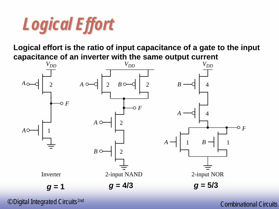
Logical EffortLogical EffortLogical effort is the ratio of input capacitance of a gate to the inputcapacitance of an inverter with the same output current
B
A
A B
g = 1 g = 4/3 g = 5/3
F
VDDVDD
A B
A
B
F
VDD
A
A
F
1
2 2 2
2
21 1
4
4
Inverter 2-input NAND 2-input NOR

EE141107
© Digital Integrated Circuits2nd Combinational Circuits
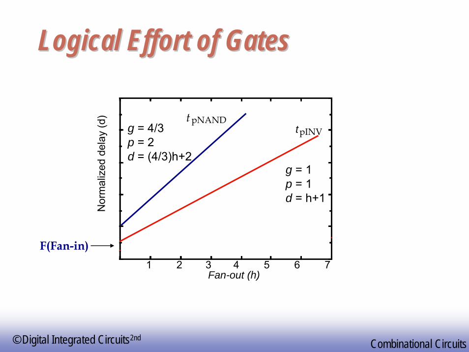
Logical Effort of GatesLogical Effort of Gates
Fan-out (h)
t
Nor
mal
ized
del
ay (d
)
1 2 3 4 5 6 7
pINVt pNAND
F(Fan-in)
g =p =d =
g =p =d =
EE141108
© Digital Integrated Circuits2nd Combinational Circuits
Logical Effort of GatesLogical Effort of Gates
Fan-out (h)
t
Nor
mal
ized
del
ay (d
)
1 2 3 4 5 6 7
pINVt pNAND
F(Fan-in)
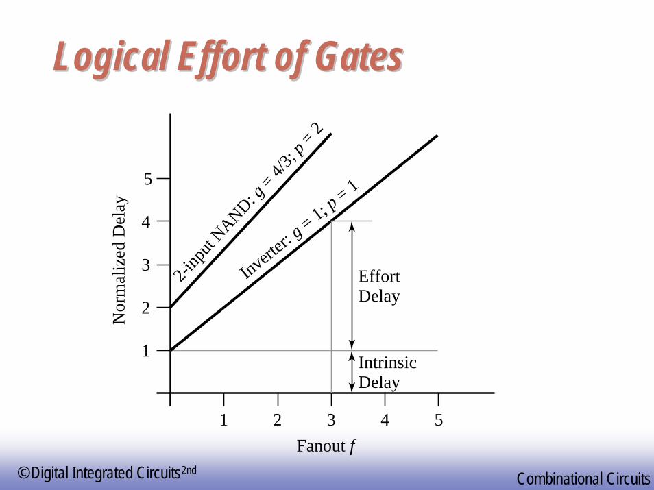
g = 1p = 1d = h+1
g = 4/3p = 2d = (4/3)h+2
EE141109
© Digital Integrated Circuits2nd Combinational Circuits
Logical Effort of GatesLogical Effort of Gates
Intrinsic�Delay
EffortDelay
1 2 3 4 5Fanout f
1
2
3
4
5
Inverter:
g = 1; p = 12-i
nput
NAND: g = 4/
3;p =
2
Nor
mal
ized
Del
ay
EE141110
© Digital Integrated Circuits2nd Combinational Circuits
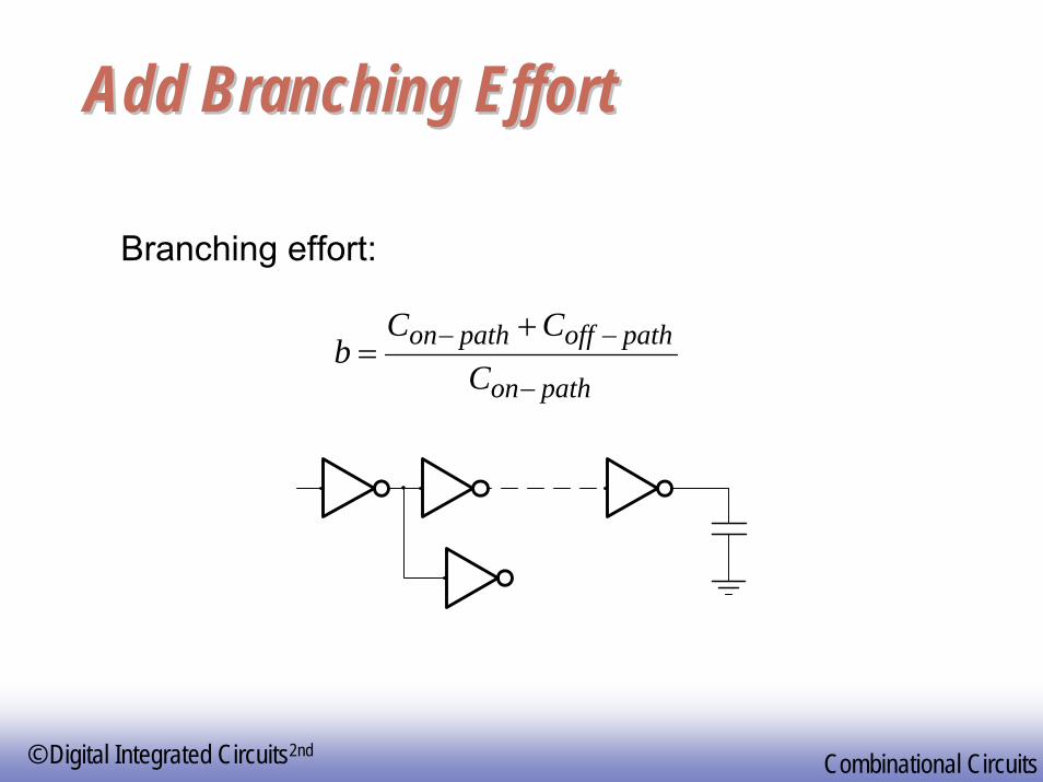
Add Branching EffortAdd Branching Effort
Branching effort:
pathon
pathoffpathonC
CCb
−
−− +=

EE141111
© Digital Integrated Circuits2nd Combinational Circuits
Multistage NetworksMultistage Networks
Stage effort: hi = gifiPath electrical effort: F = Cout/Cin
Path logical effort: G = g1g2…gN
Branching effort: B = b1b2…bN
Path effort: H = GFB
Path delay D = Σdi = Σpi + Σhi
( )∑=
⋅+=N
iiii fgpDelay
1
EE141112
© Digital Integrated Circuits2nd Combinational Circuits
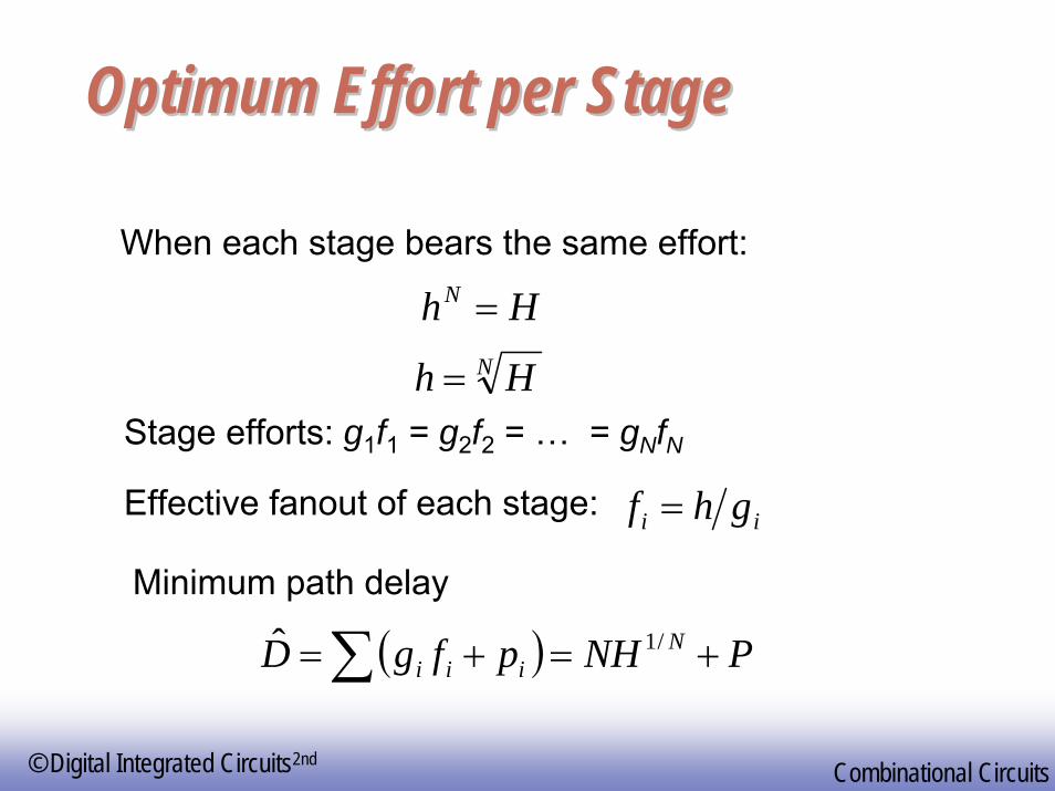
Optimum Effort per StageOptimum Effort per Stage
HhN =
When each stage bears the same effort:
N Hh =
( ) PNHpfgD Niii +=+= ∑ /1ˆ
Minimum path delay
Effective fanout of each stage: ii ghf =
Stage efforts: g1f1 = g2f2 = … = gNfN
EE141113
© Digital Integrated Circuits2nd Combinational Circuits
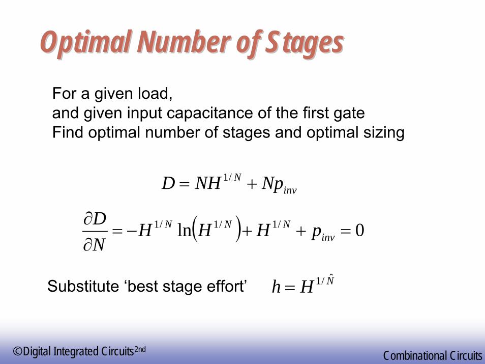
Optimal Number of StagesOptimal Number of StagesFor a given load, and given input capacitance of the first gateFind optimal number of stages and optimal sizing
invN NpNHD += /1
( ) 0ln /1/1/1 =++−=∂∂
invNNN pHHH
ND
NHh ˆ/1=Substitute ‘best stage effort’

EE141114
© Digital Integrated Circuits2nd Combinational Circuits
Logical EffortLogical Effort
From Sutherland, Sproull
EE141115
© Digital Integrated Circuits2nd Combinational Circuits
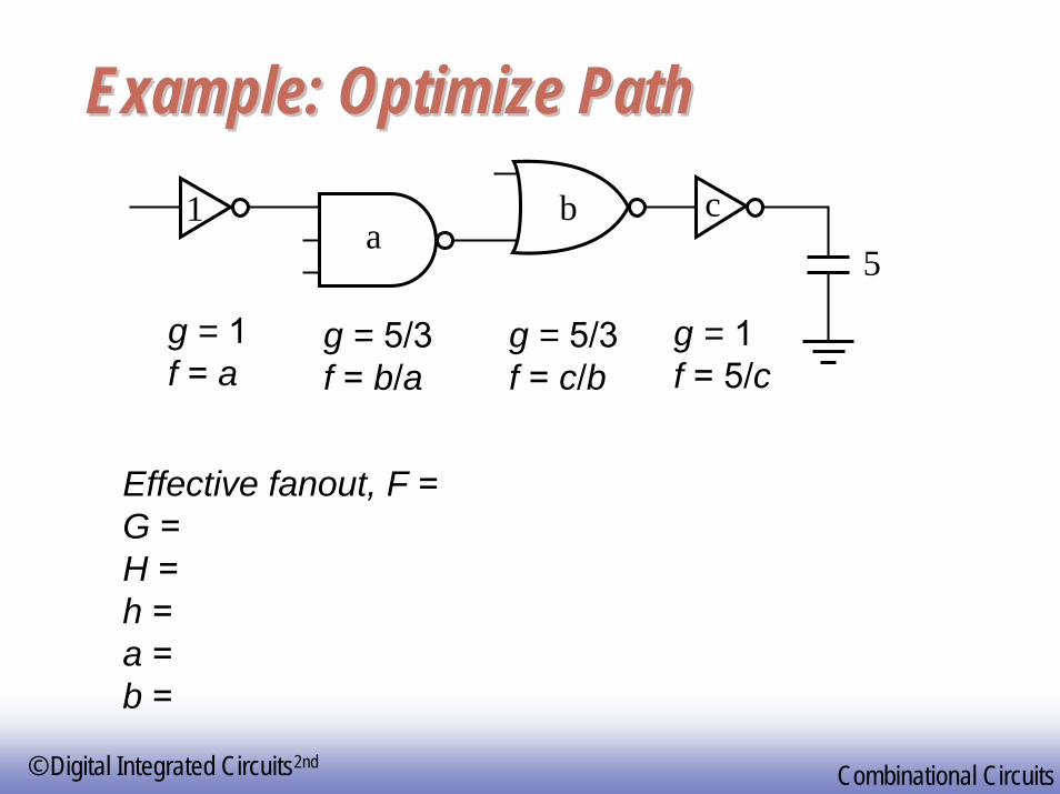
Example: Optimize PathExample: Optimize Path
Effective fanout, F =G = H =h =a =b =
1a
b c
5
g = 1f = a
g = 5/3f = b/a
g = 5/3f = c/b
g = 1f = 5/c
EE141116
© Digital Integrated Circuits2nd Combinational Circuits
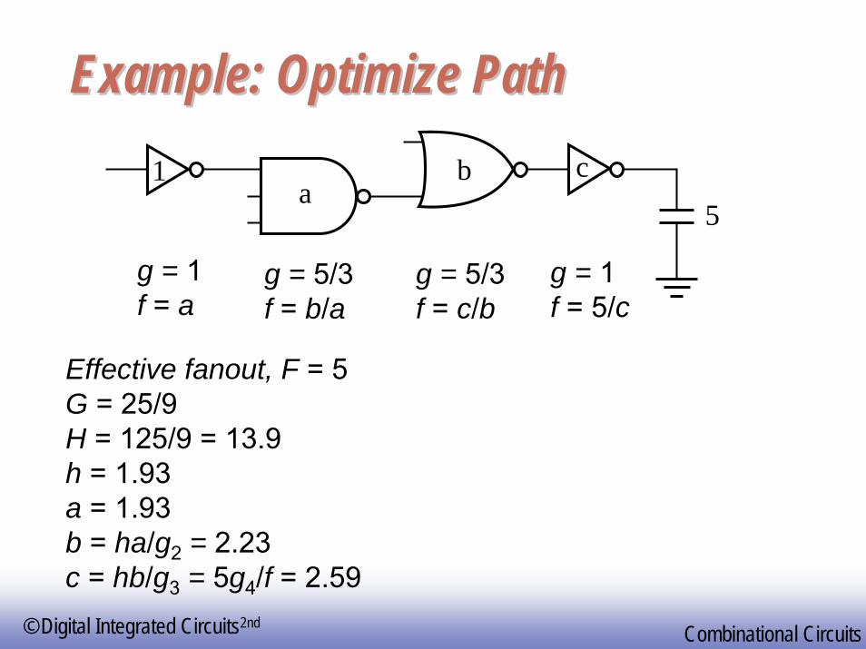
Example: Optimize PathExample: Optimize Path1
ab c
5
g = 1f = a
g = 5/3f = b/a
g = 5/3f = c/b
g = 1f = 5/c
Effective fanout, F = 5G = 25/9H = 125/9 = 13.9h = 1.93a = 1.93b = ha/g2 = 2.23c = hb/g3 = 5g4/f = 2.59

EE141117
© Digital Integrated Circuits2nd Combinational Circuits
Example: Optimize PathExample: Optimize Path
1 a
b c 5
Effective fanout, H = 5G = 25/9F = 125/9 = 13.9f = 1.93a = 1.93b = fa/g2 = 2.23c = fb/g3 = 5g4/f = 2.59
g1 = 1 g2 = 5/3 g3 = 5/3 g4 = 1
EE141118
© Digital Integrated Circuits2nd Combinational Circuits
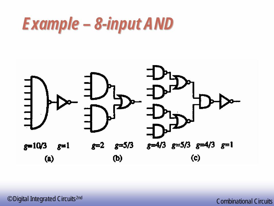
Example Example –– 88--input ANDinput AND
EE141119
© Digital Integrated Circuits2nd Combinational Circuits
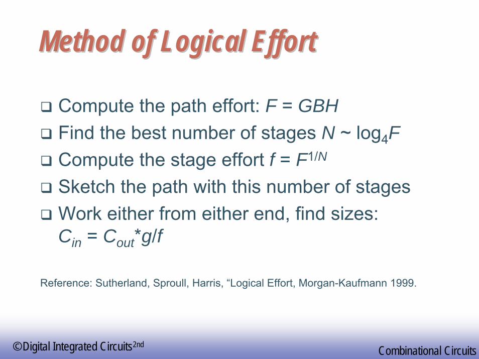
Method of Logical EffortMethod of Logical Effort
Compute the path effort: F = GBHFind the best number of stages N ~ log4FCompute the stage effort f = F1/N
Sketch the path with this number of stagesWork either from either end, find sizes: Cin = Cout*g/f
Reference: Sutherland, Sproull, Harris, “Logical Effort, Morgan-Kaufmann 1999.

EE141120
© Digital Integrated Circuits2nd Combinational Circuits
SummarySummary
Sutherland,SproullHarris

EE141121
© Digital Integrated Circuits2nd Combinational Circuits
RatioedRatioed LogicLogic

EE141122
© Digital Integrated Circuits2nd Combinational Circuits
RatioedRatioed LogicLogic
VDD
VSS
PDNIn1In2In3
F
RLLoad
VDD
VSS
In1In2In3
F
VDD
VSS
PDNIn1In2In3
FVSS
PDN
Resistive DepletionLoad
PMOSLoad
(a) resistive load (b) depletion load NMOS (c) pseudo-NMOS
VT < 0
Goal: to reduce the number of devices over complementary CMOS

EE141123
© Digital Integrated Circuits2nd Combinational Circuits
RatioedRatioed LogicLogicVDD
VSS
PDNIn1In2In3
F
RLLoadResistive
N transistors + Load
• VOH = VDD
• VOL = RPN
RPN + RL
• Assymetrical response
• Static power consumption
•
• tpL= 0.69 RLCL
EE141124
© Digital Integrated Circuits2nd Combinational Circuits
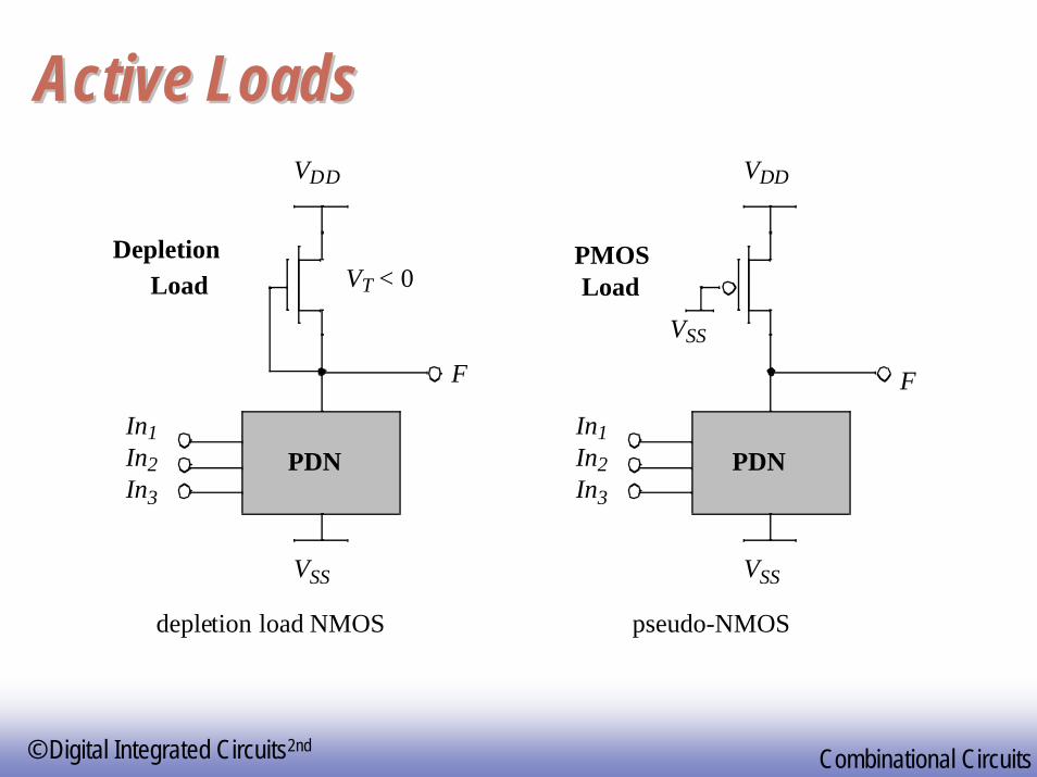
Active LoadsActive LoadsVDD
VSS
In1In2In3
F
VDD
VSS
PDNIn1In2In3
F
VSS
PDN
DepletionLoad
PMOSLoad
depletion load NMOS pseudo-NMOS
VT < 0

EE141125
© Digital Integrated Circuits2nd Combinational Circuits
PseudoPseudo--NMOSNMOS
VDD
A B C D
FCL
VOH = VDD (similar to complementary CMOS)
kn VDD VTn–( )VOLVOL
2
2-------------–
⎝ ⎠⎜ ⎟⎛ ⎞ kp
2------ VDD VTp–( )
2=
VOL VDD VT–( ) 1 1kpkn------–– (assuming that VT VTn VTp )= = =
SMALLER AREA & LOAD BUT STATIC POWER DISSIPATION!!!

EE141126
© Digital Integrated Circuits2nd Combinational Circuits
PseudoPseudo--NMOS VTCNMOS VTC
0.0 0.5 1.0 1.5 2.0 2.50.0
0.5
1.0
1.5
2.0
2.5
3.0
Vin [V]
W/Lp = 4
W/Lp = 2
W/Lp = 1
W/Lp = 0.25
Vou
t[V
]
W/Lp = 0.5
EE141127
© Digital Integrated Circuits2nd Combinational Circuits
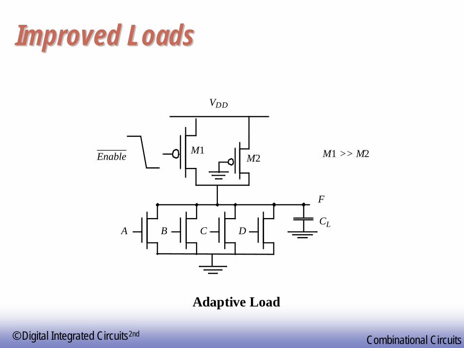
Improved LoadsImproved Loads
A B C D
F
CL
M1M2 M1 >> M2Enable
VDD
Adaptive Load

EE141128
© Digital Integrated Circuits2nd Combinational Circuits
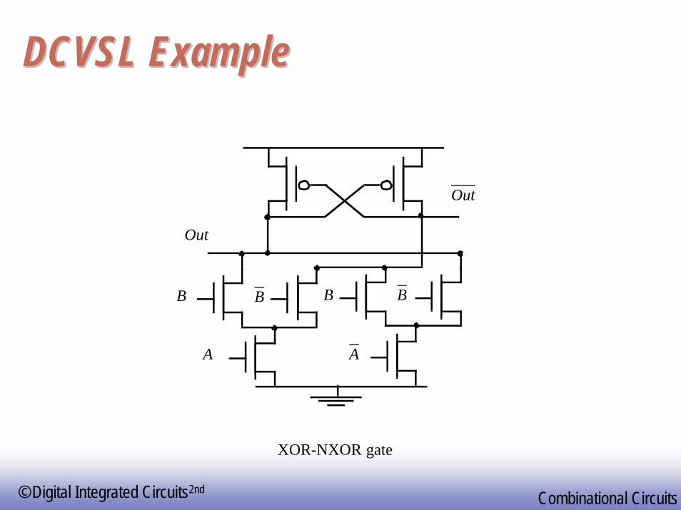
Improved Loads (2)Improved Loads (2)VDD
VSS
PDN1
Out
VDD
VSS
PDN2
Out
AABB
M1 M2
Differential Cascode Voltage Switch Logic (DCVSL)
EE141129
© Digital Integrated Circuits2nd Combinational Circuits
DCVSL ExampleDCVSL Example
B
A A
B B B
Out
Out
XOR-NXOR gate
EE141130
© Digital Integrated Circuits2nd Combinational Circuits
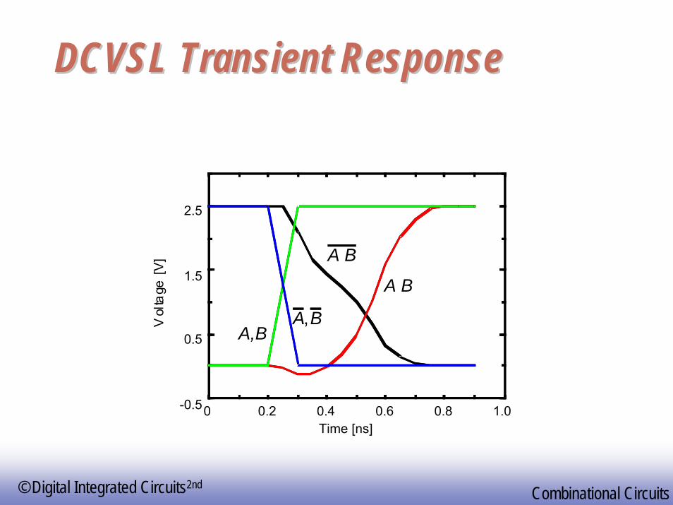
DCVSL Transient ResponseDCVSL Transient Response
0 0.2 0.4 0.6 0.8 1.0-0.5
0.5
1.5
2.5
Time [ns]
A B
Vol
tag e
[V]
A B
A,BA,B
EE141131
© Digital Integrated Circuits2nd Combinational Circuits
PassPass--TransistorTransistorLogicLogic
EE141132
© Digital Integrated Circuits2nd Combinational Circuits
PassPass--Transistor LogicTransistor LogicIn
puts Switch
Network
OutOut
A
B
B
B
• N transistors• No static consumption
EE141133
© Digital Integrated Circuits2nd Combinational Circuits
Example: AND GateExample: AND Gate
B
B
A
F = AB
0
EE141134
© Digital Integrated Circuits2nd Combinational Circuits
NMOSNMOS--Only LogicOnly Logic
VDD
In
Outx
0.5μm/0.25μm0.5μm/0.25μm
1.5μm/0.25μm
0 0.5 1 1.5 20.0
1.0
2.0
3.0
Time [ns]
xOut
In
Volt a
ge[V
]

EE141135
© Digital Integrated Circuits2nd Combinational Circuits
NMOSNMOS--only Switchonly Switch
A = 2.5 V
B
C = 2.5V
CL
A = 2.5 V
C = 2.5 V
BM2
M1
Mn
Threshold voltage loss causesstatic power consumption
VB does not pull up to 2.5V, but 2.5V -VTN
NMOS has higher threshold than PMOS (body effect)
EE141136
© Digital Integrated Circuits2nd Combinational Circuits
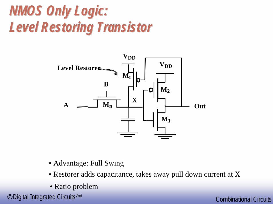
NMOS Only Logic: NMOS Only Logic: Level Restoring TransistorLevel Restoring Transistor
M2
M1
Mn
Mr
A Out
B
VDDVDDLevel Restorer
X
• Advantage: Full Swing• Restorer adds capacitance, takes away pull down current at X• Ratio problem

EE141137
© Digital Integrated Circuits2nd Combinational Circuits
Restorer SizingRestorer Sizing
0 100 200 300 400 5000.0
1.0
2.0
W/Lr =1.0/0.25 W/Lr =1.25/0.25
W/Lr =1.50/0.25
W/Lr =1.75/0.25
Vol
t ag e
[V]
Time [ps]
3.0•Upper limit on restorer size•Pass-transistor pull-downcan have several transistors in stack

EE141138
© Digital Integrated Circuits2nd Combinational Circuits
Solution 2: Single Transistor Pass Gate with Solution 2: Single Transistor Pass Gate with VVTT=0=0
Out
VDD
VDD
2.5V
VDD
0V 2.5V
0V
WATCH OUT FOR LEAKAGE CURRENTS

EE141139
© Digital Integrated Circuits2nd Combinational Circuits
Complementary Pass Transistor LogicComplementary Pass Transistor Logic
A
B
A
B
B B B B
A
B
A
B
F=AB
F=AB
F=A+B
F=A+B
B B
A
A
A
A
F=A⊕ΒÝ
F=A⊕ΒÝ
OR/NOR EXOR/NEXORAND/NAND
F
F
Pass-TransistorNetwork
Pass-TransistorNetwork
AABB
AABB
Inverse
(a)
(b)

EE141140
© Digital Integrated Circuits2nd Combinational Circuits
Solution 3: Transmission GateSolution 3: Transmission Gate
A B
C
C
A B
C
C
BCL
C = 0 V
A = 2.5 V
C = 2.5 V

EE141141
© Digital Integrated Circuits2nd Combinational Circuits
Resistance of Transmission GateResistance of Transmission Gate
Vout
0 V
2.5 V
2.5 VRn
Rp
0.0 1.0 2.00
10
20
30
Vout, V
Res
ista
nce,
ohm
s
Rn
Rp
Rn || Rp
EE141142
© Digital Integrated Circuits2nd Combinational Circuits
PassPass--Transistor Based MultiplexerTransistor Based Multiplexer
AM2
M1
B
S
S
S F
VDD
GND
VDD
In1 In2S S
S S
EE141143
© Digital Integrated Circuits2nd Combinational Circuits
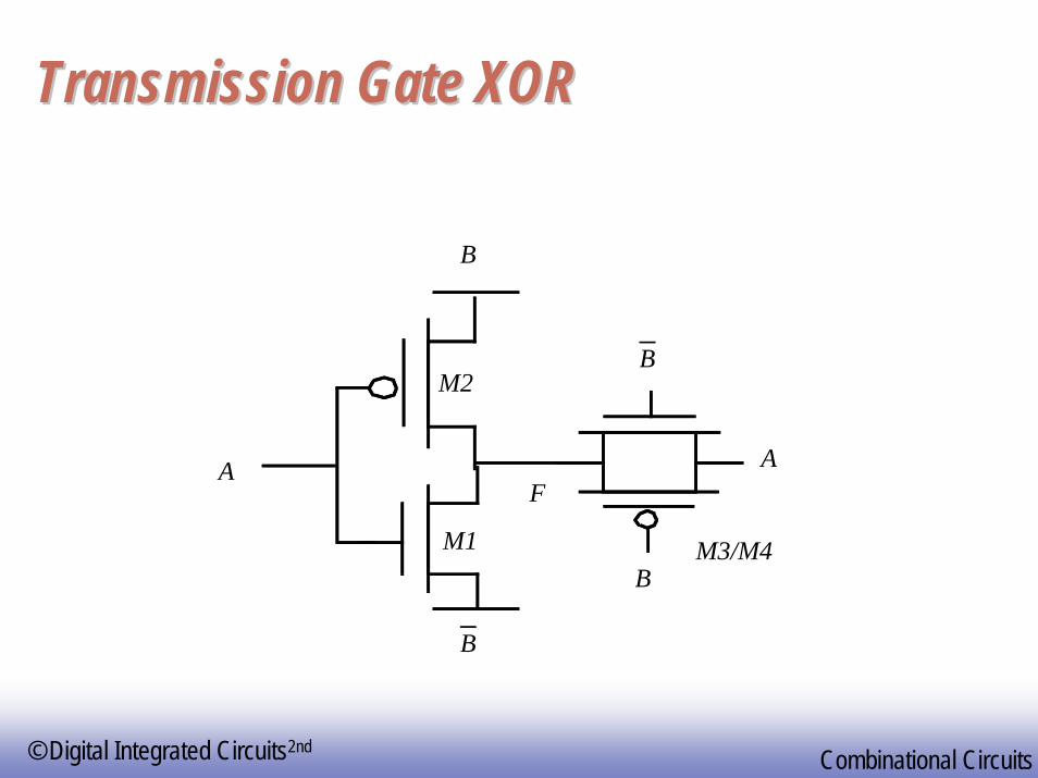
Transmission Gate XORTransmission Gate XOR
A
B
F
B
A
B
BM1
M2
M3/M4

EE141144
© Digital Integrated Circuits2nd Combinational Circuits
Delay in Transmission Gate NetworksDelay in Transmission Gate Networks
V1 Vi-1
C
2.5 2.5
0 0
Vi Vi+1
CC
2.5
0
Vn-1 Vn
CC
2.5
0
In
V1 Vi Vi+1
C
Vn-1 Vn
CC
InReqReq Req Req
CC
(a)
(b)
C
Req Req
C C
Req
C C
Req Req
C C
Req
CIn
m
(c)
EE141145
© Digital Integrated Circuits2nd Combinational Circuits
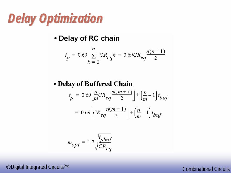
Delay OptimizationDelay Optimization

EE141146
© Digital Integrated Circuits2nd Combinational Circuits
Transmission Gate Full AdderTransmission Gate Full Adder
A
B
P
Ci
VDDA
A A
VDD
Ci
A
P
AB
VDD
VDD
Ci
Ci
Co
S
Ci
P
P
P
P
P
Sum Generation
Carry Generation
Setup
Similar delays for sum and carry

EE141147
© Digital Integrated Circuits2nd Combinational Circuits
Dynamic LogicDynamic Logic

EE141148
© Digital Integrated Circuits2nd Combinational Circuits
Dynamic CMOSDynamic CMOS
In static circuits at every point in time (except when switching) the output is connected to either GND or VDD via a low resistance path.
fan-in of n requires 2n (n N-type + n P-type) devices
Dynamic circuits rely on the temporary storage of signal values on the capacitance of high impedance nodes.
requires on n + 2 (n+1 N-type + 1 P-type) transistors

EE141149
© Digital Integrated Circuits2nd Combinational Circuits
Dynamic GateDynamic Gate
In1
In2 PDN
Me
Mp
In3
Clk
ClkOut
CL
Out
Clk
Clk
A
BC
Mp
Me
on
off
1off
on
((AB)+C)
Two phase operationPrecharge (Clk = 0)Evaluate (Clk = 1)
EE141150
© Digital Integrated Circuits2nd Combinational Circuits
Conditions on OutputConditions on Output
Once the output of a dynamic gate is discharged, it cannot be charged again until the next precharge operation.Inputs to the gate can make at most one transition during evaluation.
Output can be in the high impedance state during and after evaluation (PDN off), state is stored on CL

EE141151
© Digital Integrated Circuits2nd Combinational Circuits
Properties of Dynamic GatesProperties of Dynamic GatesLogic function is implemented by the PDN only
number of transistors is N + 2 (versus 2N for static complementary CMOS)
Full swing outputs (VOL = GND and VOH = VDD)Non-ratioed - sizing of the devices does not affect the logic levelsFaster switching speeds
reduced load capacitance due to lower input capacitance (Cin)reduced load capacitance due to smaller output loading (Cout)no Isc, so all the current provided by PDN goes into discharging CL

EE141152
© Digital Integrated Circuits2nd Combinational Circuits
Properties of Dynamic GatesProperties of Dynamic GatesOverall power dissipation usually higher than static CMOS
no static current path ever exists between VDD and GND (including Psc)no glitchinghigher transition probabilitiesextra load on Clk
PDN starts to work as soon as the input signals exceed VTn, so VM, VIH and VIL equal to VTn
low noise margin (NML)Needs a precharge/evaluate clock

EE141153
© Digital Integrated Circuits2nd Combinational Circuits
Issues in Dynamic Design 1: Issues in Dynamic Design 1: Charge LeakageCharge Leakage
CL
Clk
ClkOut
Mp
Me
A
Leakage sources
CLK
VOut
Precharge
Evaluate
Dominant component is subthreshold current
EE141154
© Digital Integrated Circuits2nd Combinational Circuits
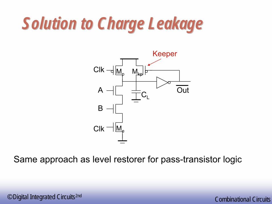
Solution to Charge LeakageSolution to Charge Leakage
CL
Clk
Clk
Me
Mp
Out
Mkp
Keeper
A
B
Same approach as level restorer for pass-transistor logic
EE141155
© Digital Integrated Circuits2nd Combinational Circuits
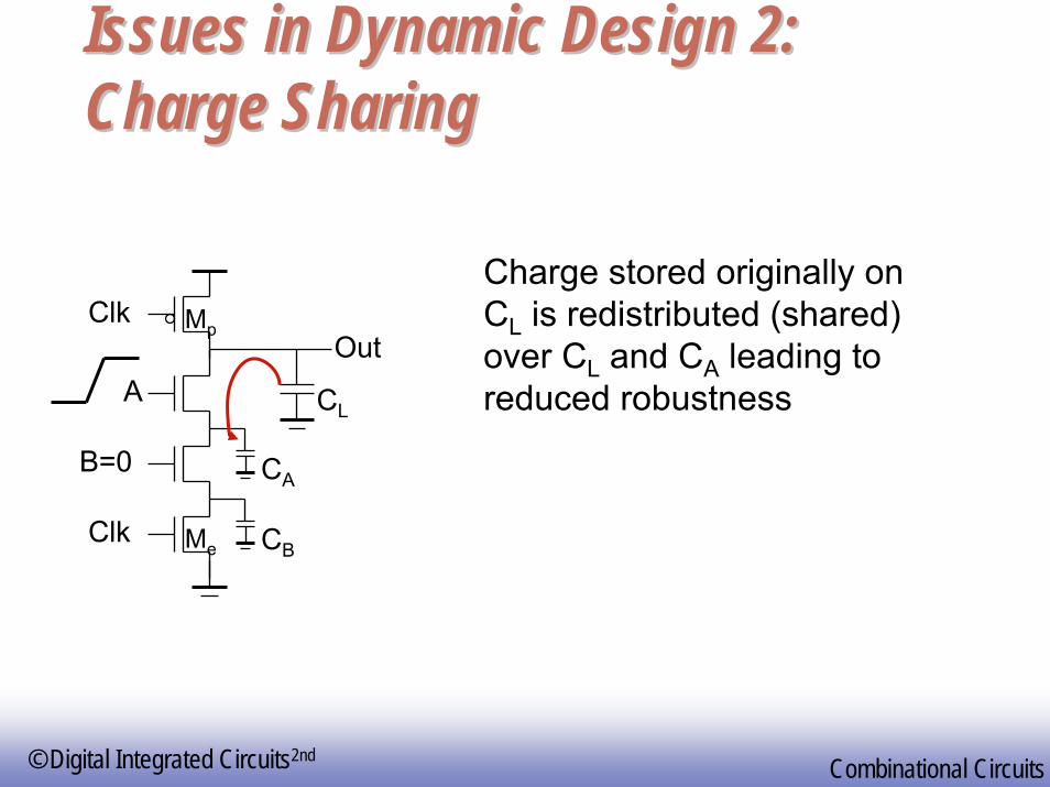
Issues in Dynamic Design 2: Issues in Dynamic Design 2: Charge SharingCharge Sharing
CL
Clk
Clk
CA
CB
A
B=0
OutMp
Me
Charge stored originally on CL is redistributed (shared) over CL and CA leading to reduced robustness

EE141156
© Digital Integrated Circuits2nd Combinational Circuits
Charge Sharing ExampleCharge Sharing Example
CL=50fF
Clk
Clk
A A
B B B !B
CC
Out
Ca=15fF
Cc=15fF
Cb=15fF
Cd=10fF
EE141157
© Digital Integrated Circuits2nd Combinational Circuits
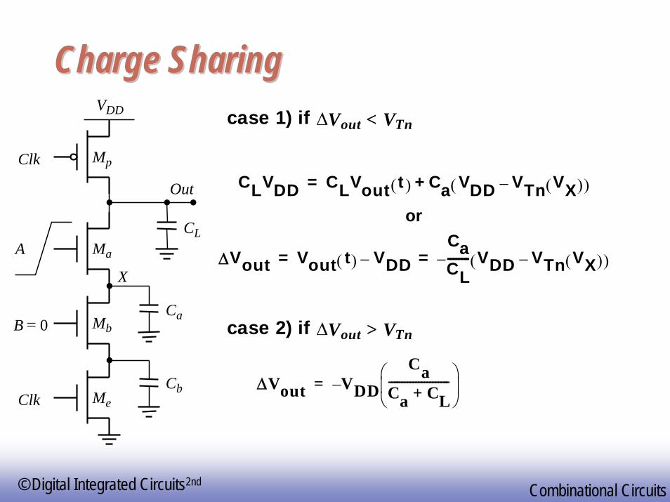
Charge SharingCharge Sharing
CLVDD CLVout t( ) Ca VDD VTn VX( )–( )+=
or
ΔVout Vout t( ) VDD–CaCL-------- VDD VTn VX( )–( )–= =
ΔVout VDDCa
Ca CL+----------------------
⎝ ⎠⎜ ⎟⎛ ⎞
–=
case 1) if ΔVout < VTn
case 2) if ΔVout > VTn
X
CL
Ca
Cb
Out
B = 0
Clk
A
Mp
Ma
VDD
Mb
Clk Me

EE141158
© Digital Integrated Circuits2nd Combinational Circuits
Solution to Charge RedistributionSolution to Charge Redistribution
Clk
Clk
Me
Mp
OutMkp
A
B
Clk
Precharge internal nodes using a clock-driven transistor (at the cost of increased area and power)
EE141159
© Digital Integrated Circuits2nd Combinational Circuits
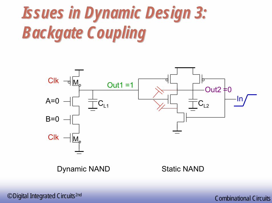
Issues in Dynamic Design 3: Issues in Dynamic Design 3: BackgateBackgate CouplingCoupling
CL1
Clk
Clk
B=0
A=0
Out1Mp
Me
Out2
CL2In
Dynamic NAND Static NAND
=1 =0

EE141160
© Digital Integrated Circuits2nd Combinational Circuits
BackgateBackgate Coupling EffectCoupling Effect
-1
0
1
2
3
0 2 4 6
Vol
tage
Time, ns
Clk
In
Out1
Out2

EE141161
© Digital Integrated Circuits2nd Combinational Circuits
Issues in Dynamic Design 4: Clock Issues in Dynamic Design 4: Clock FeedthroughFeedthrough
CL
Clk
Clk
B
AOut
Mp
Me
Coupling between Out and Clk input of the prechargedevice due to the gate to drain capacitance. So voltage of Out can rise above VDD. The fast rising (and falling edges) of the clock couple to Out.

EE141162
© Digital Integrated Circuits2nd Combinational Circuits
Clock Clock FeedthroughFeedthrough
-0.5
0.5
1.5
2.5
0 0.5 1
Clk
Clk
In1
In2
In3
In4
Out
In &Clk
Out
Time, ns
Vol
tage
Clock feedthrough
Clock feedthrough

EE141163
© Digital Integrated Circuits2nd Combinational Circuits
Other EffectsOther Effects
Capacitive couplingSubstrate couplingMinority charge injectionSupply noise (ground bounce)

EE141164
© Digital Integrated Circuits2nd Combinational Circuits
Cascading Dynamic GatesCascading Dynamic Gates
Clk
Clk
Out1
Mp
Me
In
Mp
Me
Clk
Clk
Out2
V
t
Clk
In
Out1
Out2 ΔV
VTn
Only 0 → 1 transitions allowed at inputs!
EE141165
© Digital Integrated Circuits2nd Combinational Circuits
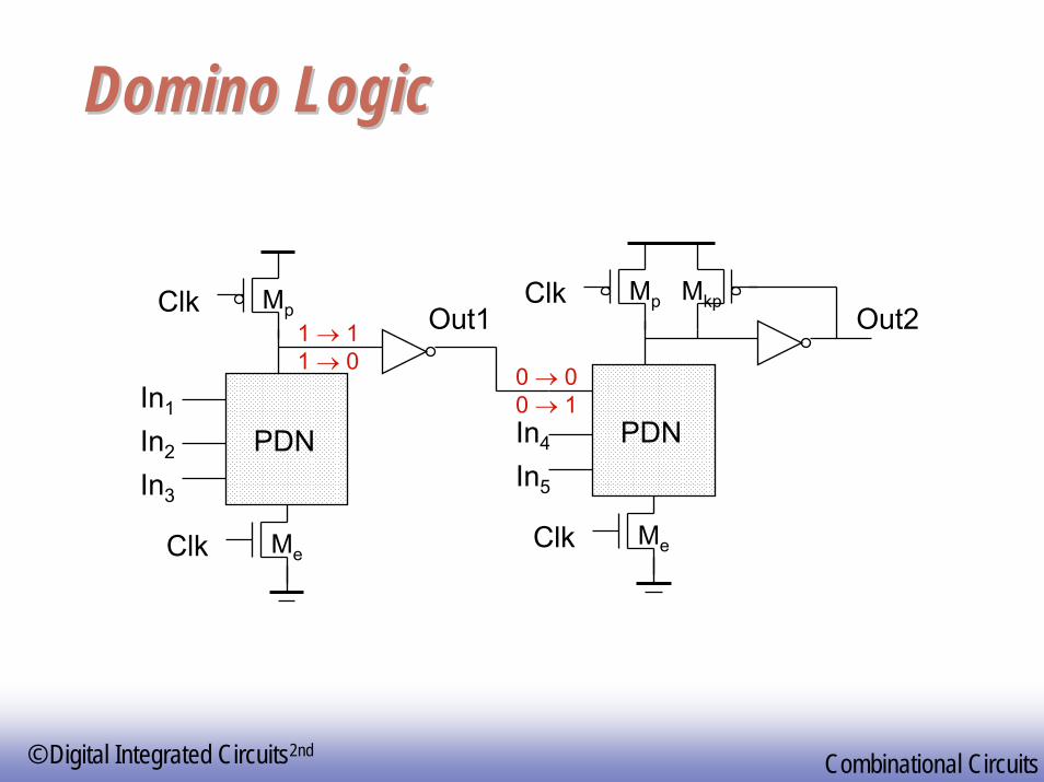
Domino LogicDomino Logic
In1
In2 PDN
Me
Mp
In3
Clk
Clk Out1
In4 PDNIn5
Me
Mp
Clk
ClkOut2
Mkp
1 → 11 → 0
0 → 00 → 1

EE141166
© Digital Integrated Circuits2nd Combinational Circuits
Why Domino?Why Domino?
Clk
Clk
Ini PDNInj
IniInj
PDN Ini PDNInj
Ini PDNInj
Like falling dominos!
EE141167
© Digital Integrated Circuits2nd Combinational Circuits
Properties of Domino LogicProperties of Domino Logic
Only non-inverting logic can be implementedVery high speed
static inverter can be skewed, only L-H transitionInput capacitance reduced – smaller logical effort
EE141168
© Digital Integrated Circuits2nd Combinational Circuits
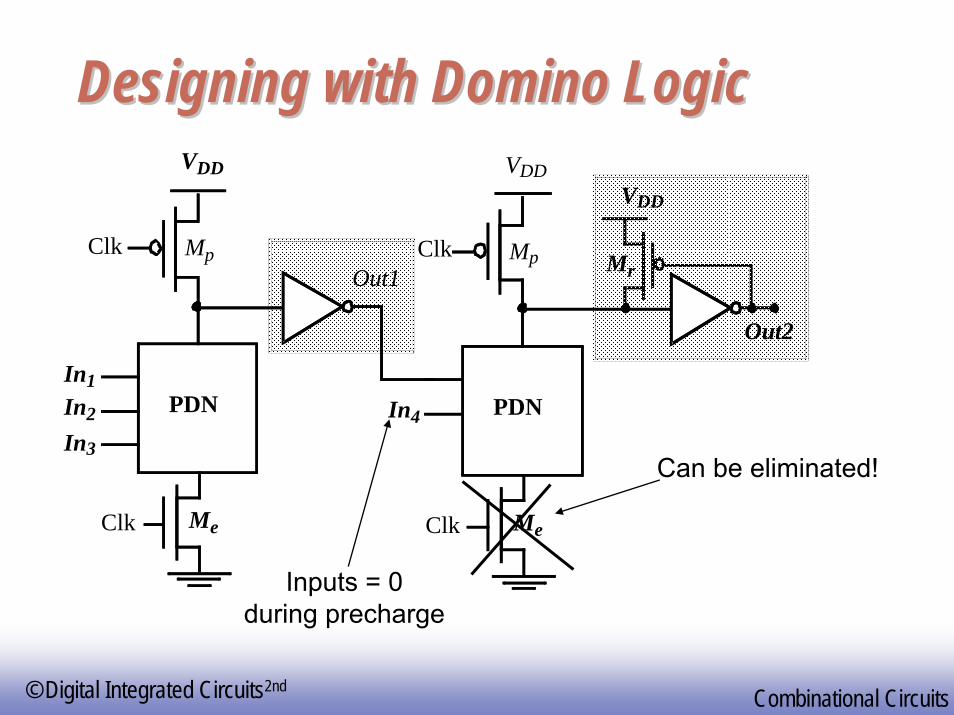
Designing with Domino LogicDesigning with Domino Logic
Mp
Me
VDD
PDN
Clk
In1In2
In3
Out1
Clk
Mp
Me
VDD
PDN
Clk
In4
Clk
Out2
Mr
VDD
Inputs = 0during precharge
Can be eliminated!

EE141169
© Digital Integrated Circuits2nd Combinational Circuits
Footless DominoFootless Domino
The first gate in the chain needs a foot switchPrecharge is rippling – short-circuit currentA solution is to delay the clock for each stage
VDD
Clk Mp
Out1
In1
1 0
VDD
Clk Mp
Out2
In2
VDD
Clk Mp
Outn
InnIn3
1 0
0 1 0 1 0 1
1 0 1 0
EE141170
© Digital Integrated Circuits2nd Combinational Circuits
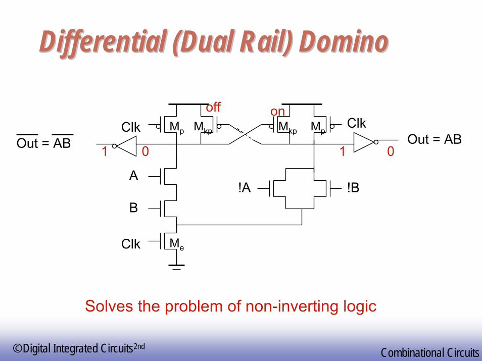
Differential (Dual Rail) DominoDifferential (Dual Rail) Domino
A
B
Me
MpClk
Clk
Out = AB
!A !B
MkpClk
Out = ABMkp Mp
Solves the problem of non-inverting logic
1 0 1 0
onoff
EE141171
© Digital Integrated Circuits2nd Combinational Circuits
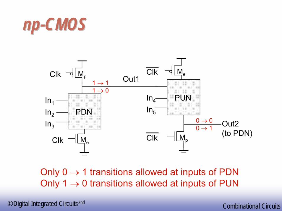
npnp--CMOSCMOS
In1
In2 PDN
Me
Mp
In3
Clk
Clk Out1
In4 PUNIn5
Me
MpClk
Clk
Out2(to PDN)
1 → 11 → 0
0 → 00 → 1
Only 0 → 1 transitions allowed at inputs of PDN Only 1 → 0 transitions allowed at inputs of PUN
EE141172
© Digital Integrated Circuits2nd Combinational Circuits
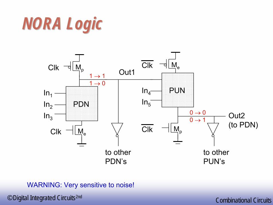
NORA LogicNORA Logic
In1
In2 PDN
Me
Mp
In3
Clk
Clk Out1
In4 PUNIn5
Me
MpClk
Clk
Out2(to PDN)
1 → 11 → 0
0 → 00 → 1
to otherPDN’s
to otherPUN’s
WARNING: Very sensitive to noise!