Embed Size (px)
Citation preview
JEDEC STANDARD
DDR4 SDRAM
JESD79-4B (Revision of JESD79-4A, November 2013) JUNE 2017 JEDEC SOLID STATE TECHNOLOGY ASSOCIATION

NOTICE
JEDEC standards and publications contain material that has been prepared, reviewed, and approved through the JEDEC Board of Directors level and subsequently reviewed and approved
by the JEDEC legal counsel.
JEDEC standards and publications are designed to serve the public interest through eliminating misunderstandings between manufacturers and purchasers, facilitating interchangeability and
improvement of products, and assisting the purchaser in selecting and obtaining with minimum delay the proper product for use by those other than JEDEC members, whether the standard is to
be used either domestically or internationally.
JEDEC standards and publications are adopted without regard to whether or not their adoption may involve patents or articles, materials, or processes. By such action JEDEC does not assume any liability to any patent owner, nor does it assume any obligation whatever to parties adopting
the JEDEC standards or publications.
The information included in JEDEC standards and publications represents a sound approach to product specification and application, principally from the solid state device manufacturer
viewpoint. Within the JEDEC organization there are procedures whereby a JEDEC standard or publication may be further processed and ultimately become an ANSI standard.
No claims to be in conformance with this standard may be made unless all requirements stated in
the standard are met.
Inquiries, comments, and suggestions relative to the content of this JEDEC standard or publication should be addressed to JEDEC at the address below, or refer to www.jedec.org under
Standards and Documents for alternative contact information.
Published by ©JEDEC Solid State Technology Association 2017
3103 North 10th Street Suite 240 South
Arlington, VA 22201-2107
This document may be downloaded free of charge; however JEDEC retains the copyright on this material. By downloading this file the individual agrees not to
charge for or resell the resulting material.
PRICE: Contact JEDEC
Printed in the U.S.A. All rights reserved
PLEASE!
DON’T VIOLATE THE
LAW!
This document is copyrighted by JEDEC and may not be reproduced without permission.
For information, contact:
JEDEC Solid State Technology Association
3103 North 10th Street Suite 240 South
Arlington, VA 22201-2107
or refer to www.jedec.org under Standards-Documents/Copyright Information.

JEDEC Standard No. 79-4B
DDR4 SDRAM STANDARD
1 Scope ............................................................................................................................................................................12 DDR4 SDRAM Package Pinout and Addressing ......................................................................................................22.1 DDR4 SDRAM Row for X4, X8 and X16.......................................................................................................................22.2 DDR4 SDRAM Ball Pitch ...............................................................................................................................................22.3 DDR4 SDRAM Columns for X4,X8 and X16..................................................................................................................22.4 DDR4 SDRAM X4/8 Ballout using MO-207 ................................................................................................................ 22.5 DDR4 SDRAM X16 Ballout using MO-207 ....................................................................................................................32.6 DDR4 SDRAM X32 Ballout using MO-XXX ...................................................................................................................42.7 Pinout Description..........................................................................................................................................................62.8 DDR4 SDRAM Addressing.............................................................................................................................................72.9 DDP Single Rank(SR) x16 from two x8 .........................................................................................................................93 Functional Description .............................................................................................................................................113.1 Simplified State Diagram .......................................................................................................................................... 113.2 Basic Functionality .......................................................................................................................................................123.3 RESET and Initialization Procedure.............................................................................................................................123.3.1 Power-up Initialization Sequence ..............................................................................................................................123.3.2 VDD Slew rate at Power-up Initialization Sequence .................................................................................................133.3.3 Reset Initialization with Stable Power .......................................................................................................................143.4 Register Definition........................................................................................................................................................143.4.1 Programming the mode registers ..............................................................................................................................143.5 Mode Register..............................................................................................................................................................174 DDR4 SDRAM Command Description and Operation ...........................................................................................284.1 Command Truth Table..................................................................................................................................................284.2 CKE Truth Table ...........................................................................................................................................................294.3 Burst Length, Type and Order......................................................................................................................................304.3.1 BL8 Burst order with CRC Enabled ...........................................................................................................................304.4 DLL-off Mode & DLL on/off Switching procedure ........................................................................................................314.4.1 DLL on/off switching procedure .................................................................................................................................314.4.2 DLL “on” to DLL “off” Procedure ................................................................................................................................314.4.3 DLL “off” to DLL “on” Procedure ................................................................................................................................324.5 DLL-off Mode ...............................................................................................................................................................334.6 Input Clock Frequency Change ...................................................................................................................................344.7 Write Leveling ..............................................................................................................................................................354.7.1 DRAM setting for write leveling & DRAM termination function in that mode .............................................................364.7.2 Procedure Description................................................................................................................................................364.7.3 Write Leveling Mode Exit............................................................................................................................................374.8 Temperature controlled Refresh modes.......................................................................................................................384.8.1 Normal temperature mode ( 0°C =< TCASE =< 85°C ) ............................................................................................384.8.2 Extended temperature mode ( 0°C =< TCASE =< 95°C ) .........................................................................................384.9 Fine Granularity Refresh Mode....................................................................................................................................394.9.1 Mode Register and Command Truth Table................................................................................................................394.9.2 tREFI and tRFC parameters.......................................................................................................................................404.9.3 Changing Refresh Rate..............................................................................................................................................404.9.4 Usage with Temperature Controlled Refresh mode...................................................................................................414.9.5 Self Refresh entry and exit .........................................................................................................................................414.10 Multi Purpose Register ................................................................................................................................................414.10.1 DQ Training with MPR..............................................................................................................................................414.10.2 MR3 definition .........................................................................................................................................................414.10.3 MPR Reads .............................................................................................................................................................424.10.4 MPR Writes .............................................................................................................................................................444.10.5 MPR Read Data format ...........................................................................................................................................474.11 Data Mask(DM), Data Bus Inversion (DBI) and TDQS................................................................................................52
Contents
-i-
JEDEC Standard No. 79-4B
4.12 ZQ Calibration Commands ......................................................................................................................................... 544.12.1 ZQ Calibration Description ...................................................................................................................................... 544.13 DQ Vref Training ......................................................................................................................................................... 554.13.1 Example scripts for VREFDQ Calibration Mode ..................................................................................................... 584.14 Per DRAM Addressability ........................................................................................................................................... 614.15 CAL Mode (CS_n to Command Address Latency) ..................................................................................................... 614.15.1 CAL Mode Description ............................................................................................................................................ 634.15.2 Self Refresh Entry, Exit Timing with CAL ................................................................................................................ 664.15.3 Power Down Entry, Exit Timing with CAL ............................................................................................................... 664.16 CRC............................................................................................................................................................................ 684.16.1 CRC Polynomial and logic equation ....................................................................................................................... 684.16.2 CRC data bit mapping for x8 devices ..................................................................................................................... 694.16.3 CRC data bit mapping for x4 devices ..................................................................................................................... 694.16.4 CRC data bit mapping for x16 devices ................................................................................................................... 694.16.5 Write CRC for x4, x8 and x16 devices .................................................................................................................... 704.16.6 CRC Error Handling ................................................................................................................................................ 704.16.7 CRC Frame format with BC4 .................................................................................................................................. 714.16.8 Simultaneous DM and CRC Functionality .............................................................................................................. 734.16.9 Simultaneous MPR Write, Per DRAM Addressability and CRC Functionality ........................................................ 734.17 Command Address Parity (CA Parity)......................................................................................................................... 744.17.1 CA Parity Error Log Readout .................................................................................................................................. 804.18 Control Gear-down Mode ........................................................................................................................................... 814.19 DDR4 Key Core Timing .............................................................................................................................................. 834.20 Programmable Preamble............................................................................................................................................ 864.20.1 Write Preamble ....................................................................................................................................................... 864.20.2 Read Preamble ....................................................................................................................................................... 884.20.3 Read Preamble Training ......................................................................................................................................... 884.21 Postamble................................................................................................................................................................... 894.21.1 Read Postamble ..................................................................................................................................................... 894.21.2 Write Postamble ..................................................................................................................................................... 894.22 ACTIVATE Command ................................................................................................................................................. 894.23 Precharge Command ................................................................................................................................................. 894.24 Read Operation .......................................................................................................................................................... 904.24.1 READ Timing Definitions ........................................................................................................................................ 904.24.1.1 READ Timing; Clock to Data Strobe relationship ................................................................................................. 924.24.1.2 READ Timing; Data Strobe to Data relationship ................................................................................................... 934.24.1.3 tLZ(DQS), tLZ(DQ), tHZ(DQS), tHZ(DQ) Calculation ........................................................................................... 944.24.1.4 tRPRE Calculation ................................................................................................................................................ 964.24.1.5 tRPST Calculation ................................................................................................................................................ 974.24.2 READ Burst Operation ........................................................................................................................................... 984.24.3 Burst Read Operation followed by a Precharge ................................................................................................... 1094.24.4 Burst Read Operation with Read DBI (Data Bus Inversion) ................................................................................. 1114.24.5 Burst Read Operation with Command/Address Parity .......................................................................................... 1124.24.6 Read to Write with Write CRC .............................................................................................................................. 1134.24.7 Read to Read with CS to CA Latency ....................................................................................................................1144.25 Write Operation..........................................................................................................................................................1154.25.1 Write Timing Parameters .......................................................................................................................................1154.25.2 Write Data Mask ....................................................................................................................................................1164.25.3 tWPRE Calculation ................................................................................................................................................1174.25.4 tWPST Calculation .................................................................................................................................................1184.25.5 Write Burst Operation ............................................................................................................................................1194.25.6 Read and Write Command Interval ...................................................................................................................... 1344.25.7 Write Timing Violations ......................................................................................................................................... 1354.25.7.1 Motivation .......................................................................................................................................................... 1354.25.7.2 Data Setup and Hold Offset Violations .............................................................................................................. 1354.25.7.3 Strobe and Strobe to Clock Timing Violations ................................................................................................... 1354.26 Refresh Command ................................................................................................................................................... 1354.27 Self refresh Operation .............................................................................................................................................. 1374.27.1 Low Power Auto Self Refresh ............................................................................................................................... 138
-ii-
JEDEC Standard No. 79-4B
4.27.2 Self Refresh Exit with No Operation command .................................................................................................... 1394.28 Power down Mode................................................................................................................................................... 1404.28.1 Power-Down Entry and Exit .................................................................................................................................. 1404.28.2 Power-Down clarifications .................................................................................................................................... 1444.28.3 Power Down Entry and Exit timing during Command/Address Parity Mode is Enable.......................................... 1454.29 Maximum Power Saving Mode................................................................................................................................ 1464.29.1 Maximum power saving mode .............................................................................................................................. 1464.29.2 Mode entry ............................................................................................................................................................ 1464.29.3 CKE transition during the mode ............................................................................................................................ 1474.29.4 Mode exit .............................................................................................................................................................. 1474.29.5 Timing parameter bin of Maximum Power Saving Mode for DDR4-1600/1866/2133/2400/2666/3200................. 1484.30 Connectivity Test Mode ........................................................................................................................................... 1484.30.1 Introduction ........................................................................................................................................................... 1484.30.2 Pin Mapping .......................................................................................................................................................... 1484.30.3 Logic Equations .................................................................................................................................................... 1494.30.3.1 Min Term Equations ........................................................................................................................................... 1494.30.3.2 Output equations for x16 devices ...................................................................................................................... 1504.30.3.3 Output equations for x8 devices ........................................................................................................................ 15040.30.3.4 Output equations for x4 devices ...................................................................................................................... 1504.30.4 Input level and Timing Requirement ..................................................................................................................... 1514.30.5 Connectivity Test ( CT ) Mode Input Levels .......................................................................................................... 1524.30.5.1 Input Levels for RESET_n .................................................................................................................................. 1534.30.5.2 Input Levels for ALERT_n ................................................................................................................................. 1534.31 CLK to Read DQS timing parameters ..................................................................................................................... 1544.32 Post Package Repair (hPPR).................................................................................................................................. 1564.32.1 Hard Fail Row Address Repair (WRA Case) ........................................................................................................ 1564.32.2 Hard Fail Row Address Repair (WR Case) ........................................................................................................... 1574.32.3 Hard Fail Row Address Repair MR bits and timing diagram ................................................................................. 1574.32.4 Programming hPPR & sPPR support in MPR0 page2 ........................................................................................ 1584.32.5 Required Timing Parameters ................................................................................................................................ 1594.33 Soft Post Package Repair (sPPR)........................................................................................................................... 1594.33.1 Soft Repair of a Fail Row Address ........................................................................................................................ 1605 On-Die Termination ................................................................................................................................................ 1615.1 ODT Mode Register and ODT State Table ................................................................................................................ 1615.2 Synchronous ODT Mode ........................................................................................................................................... 1635.2.1 ODT Latency and Posted ODT ............................................................................................................................... 1645.2.2 Timing Parameters ................................................................................................................................................. 1645.2.3 ODT during Reads................................................................................................................................................... 1665.3 Dynamic ODT............................................................................................................................................................ 1675.3.1 Functional Description ............................................................................................................................................ 1675.3.2 ODT Timing Diagrams ............................................................................................................................................ 1685.4 Asynchronous ODT mode ......................................................................................................................................... 1695.5 ODT buffer disabled mode for Power down .............................................................................................................. 1705.6 ODT Timing Definitions.............................................................................................................................................. 1715.6.1 Test Load for ODT Timings .................................................................................................................................... 1715.6.2 ODT Timing Definitions ........................................................................................................................................... 1746 Absolute Maximum Ratings .................................................................................................................................. 1747 AC and DC Operating Conditions ......................................................................................................................... 1748 AC and DC Input Measurement Levels ................................................................................................................. 1748.1 AC and DC Logic input levels for single-ended signals............................................................................................. 1748.2 AC and DC Input Measurement Levels: VREF Tolerances ....................................................................................... 1758.3 AC and DC Logic Input Levels for Differential Signals .............................................................................................. 1768.3.1 Differential signal definition ..................................................................................................................................... 1768.3.2 Differential swing requirements for clock (CK_t - CK_c) ......................................................................................... 1768.3.3 Single-ended requirements for differential signals .................................................................................................. 1778.3.4 Address, Command and Control Overshoot and Undershoot specifications .......................................................... 1788.3.5 Clock Overshoot and Undershoot Specifications ................................................................................................... 1798.3.6 Data, Strobe and Mask Overshoot and Undershoot Specifications ........................................................................ 1808.4 Slew Rate Definitions ............................................................................................................................................... 181
--iii-
JEDEC Standard No. 79-4B
8.4.1 Slew Rate Definitions for Differential Input Signals ( CK ) ...................................................................................... 1818.4.2 Slew Rate Definition for Single-ended Input Signals ( CMD/ADD ) ........................................................................ 1828.5 Differential Input Cross Point Voltage........................................................................................................................ 1828.6 CMOS rail to rail Input Levels.................................................................................................................................... 1838.6.1 CMOS rail to rail Input Levels for RESET_n ........................................................................................................... 1838.7 AC and DC Logic Input Levels for DQS Signals........................................................................................................ 1848.7.1 Differential signal definition ..................................................................................................................................... 1848.7.2 Differential swing requirements for DQS (DQS_t - DQS_c) ................................................................................... 1848.7.3 Peak voltage calculation method ............................................................................................................................ 1858.7.4 Differential Input Cross Point Voltage ..................................................................................................................... 1868.7.5 Differential Input Slew Rate Definition .................................................................................................................... 1879 AC and DC output Measurement levels ............................................................................................................... 1889.1 Output Driver DC Electrical Characteristics............................................................................................................... 1889.1.1 Alert_n output Drive Characteristic ......................................................................................................................... 1909.1.2 Output Driver Characteristic of Connectivity Test ( CT ) Mode ............................................................................... 1919.2 Single-ended AC & DC Output Levels....................................................................................................................... 1919.3 Differential AC & DC Output Levels........................................................................................................................... 1929.4 Single-ended Output Slew Rate ................................................................................................................................ 1929.5 Differential Output Slew Rate .................................................................................................................................... 1939.6 Single-ended AC & DC Output Levels of Connectivity Test Mode............................................................................. 1949.7 Test Load for Connectivity Test Mode Timing ............................................................................................................ 19410 Speed Bin ................................................................................................................................................................ 19510.1 Speed Bin Table Note ............................................................................................................................................... 20311 IDD and IDDQ Specification Parameters and Test conditions .......................................................................... 20411.1 IDD, IPP and IDDQ Measurement Conditions .......................................................................................................... 20411.2 IDD Specifications..................................................................................................................................................... 21912 Input/Output Capacitance ...................................................................................................................................... 22113 Electrical Characteristics and AC Timing ............................................................................................................ 22413.1 Reference Load for AC Timing and Output Slew Rate ............................................................................................. 22413.2 tREFI ........................................................................................................................................................................ 22413.3 Clock Specification ................................................................................................................................................... 22513.3.1 Definition for tCK(abs) .......................................................................................................................................... 22513.3.2 Definition for tCK(avg) .......................................................................................................................................... 22513.3.3 Definition for tCH(avg) and tCL(avg) .................................................................................................................... 22513.3.4 Definition for tERR(nper) ...................................................................................................................................... 22513.4 Timing Parameters by Speed Grade ........................................................................................................................ 22613.5 Rounding Algorithms ................................................................................................................................................ 24313.6 The DQ input receiver compliance mask for voltage and timing (see Figure 211) ................................................... 24413.7 Command, Control, and Address Setup, Hold, and Derating ................................................................................... 24813.8 DDR4 Function Matrix .............................................................................................................................................. 250
-iv-
JEDEC Standard No. 79-4B Page 1
DDR4 SDRAM STANDARD
(From JEDEC Board Ballot JCB-16-56, formulated under the cognizance of the JC-42.3 Subcommittee on DRAM Memories.)
1 Scope
This document defines the DDR4 SDRAM specification, including features, functionalities, AC and DC characteristics, packages, and ball/signal assignments. The purpose of this Standard is to define the minimum set of requirements for JEDEC compliant 2 Gb through 16 Gb for x4, x8, and x16 DDR4 SDRAM devices. This standard was created based on the DDR3 standards (JESD79-3) and some aspects of the DDR and DDR2 standards (JESD79, JESD79-2).
Each aspect of the changes for DDR4 SDRAM operation were considered and approved by committee ballot(s). The accumulation of these ballots were then incorporated to prepare this JEDEC Standard, JESD79-4, replacing whole sections and incorporating the changes into Functional Description and Operation.
JEDEC Standard No. 79-4BPage 2
2 DDR4 SDRAM Package Pinout and Addressing
2.1 DDR4 SDRAM Row for X4, X8 and X16 The DDR4 SDRAM x4/x8 component will have 13 electrical rows of balls. Electrical is defined as rows that contain signal ball or power/ground balls. There may be additional rows of inactive balls for mechanical support.
The DDR4 SDRAM x16 component will have 16 electrical rows of balls. There may be additional rows of inactive balls for mechanical support.
2.2 DDR4 SDRAM Ball Pitch The DDR4 SDRAM component will use a ball pitch of 0.8 mm by 0.8 mm. The number of depopulated columns is 3.
2.3 DDR4 SDRAM Columns for X4,X8 and X16The DDR4 SDRAM x4/x8 and x16 component will have 6 electrical columns of balls in 2 sets of 3 columns. There will be columns between the electrical columns where there are no balls populated. The number of these columns is 3.
Electrical is defined as columns that contain signal ball or power/ground balls. There may be additional columns of inactive balls for mechanical support.
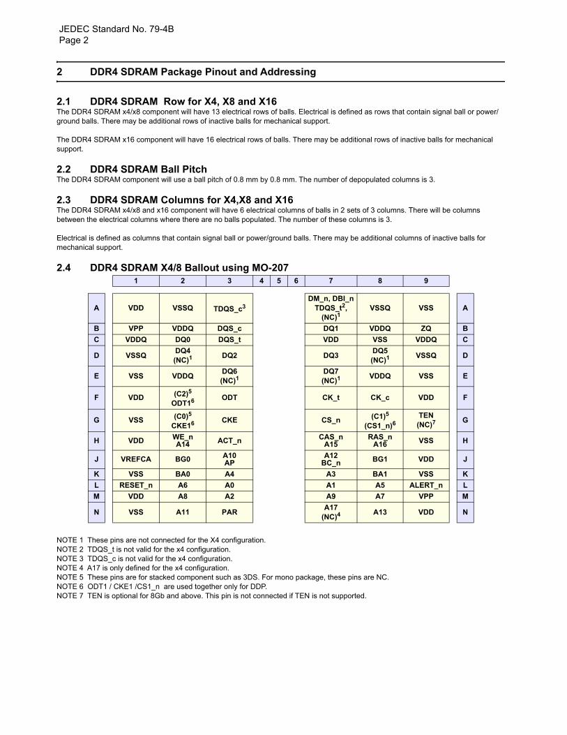
2.4 DDR4 SDRAM X4/8 Ballout using MO-207 1 2 3 4 5 6 7 8 9
A VDD VSSQ TDQS_c3DM_n, DBI_n
TDQS_t2,(NC)1
VSSQ VSS A
B VPP VDDQ DQS_c DQ1 VDDQ ZQ B
C VDDQ DQ0 DQS_t VDD VSS VDDQ C
D VSSQDQ4(NC)1
DQ2 DQ3DQ5(NC)1
VSSQ D
E VSS VDDQDQ6(NC)1
DQ7(NC)1
VDDQ VSS E
F VDD (C2)5
ODT16 ODT CK_t CK_c VDD F
G VSS (C0)5
CKE16 CKE CS_n (C1)5
(CS1_n)6TEN
(NC)7G
H VDD WE_nA14 ACT_n CAS_n
A15RAS_n
A16 VSS H
J VREFCA BG0 A10AP
A12BC_n BG1 VDD J
K VSS BA0 A4 A3 BA1 VSS K
L RESET_n A6 A0 A1 A5 ALERT_n L
M VDD A8 A2 A9 A7 VPP M
N VSS A11 PARA17
(NC)4A13 VDD N
NOTE 1 These pins are not connected for the X4 configuration.NOTE 2 TDQS_t is not valid for the x4 configuration.NOTE 3 TDQS_c is not valid for the x4 configuration.NOTE 4 A17 is only defined for the x4 configuration.NOTE 5 These pins are for stacked component such as 3DS. For mono package, these pins are NC.NOTE 6 ODT1 / CKE1 /CS1_n are used together only for DDP.NOTE 7 TEN is optional for 8Gb and above. This pin is not connected if TEN is not supported.
JEDEC Standard No. 79-4B Page 3
ure 1
Fig—DDR4 Ball Assignments for the x4/8 component
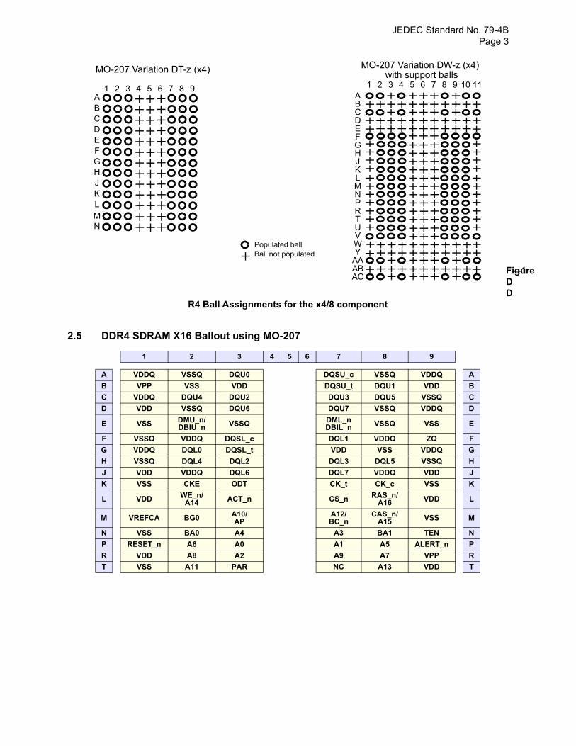
2.5 DDR4 SDRAM X16 Ballout using MO-207
1 2 3 4 5 6 7 8 9
A VDDQ VSSQ DQU0 DQSU_c VSSQ VDDQ A
B VPP VSS VDD DQSU_t DQU1 VDD B
C VDDQ DQU4 DQU2 DQU3 DQU5 VSSQ C
D VDD VSSQ DQU6 DQU7 VSSQ VDDQ D
E VSS DMU_n/DBIU_n VSSQ DML_n
DBIL_n VSSQ VSS E
F VSSQ VDDQ DQSL_c DQL1 VDDQ ZQ F
G VDDQ DQL0 DQSL_t VDD VSS VDDQ G
H VSSQ DQL4 DQL2 DQL3 DQL5 VSSQ H
J VDD VDDQ DQL6 DQL7 VDDQ VDD J
K VSS CKE ODT CK_t CK_c VSS K
L VDD WE_n/A14 ACT_n CS_n RAS_n/
A16 VDD L
M VREFCA BG0 A10/AP
A12/BC_n
CAS_n/A15 VSS M
N VSS BA0 A4 A3 BA1 TEN N
P RESET_n A6 A0 A1 A5 ALERT_n P
R VDD A8 A2 A9 A7 VPP R
T VSS A11 PAR NC A13 VDD T
1 2 3 4 8 95 6 7ABCDEFGHJKL
MO-207 Variation DT-z (x4)
Populated ballBall not populated
NM
1 2 3 4 8 95 6 7ABCDEFGHJKL
MO-207 Variation DW-z (x4)
NM
10 11
PRTUVWY
AAABAC
with support balls
JEDEC Standard No. 79-4BPage 4
Figure 2 — DDR4 Ball Assignments for the x16 component
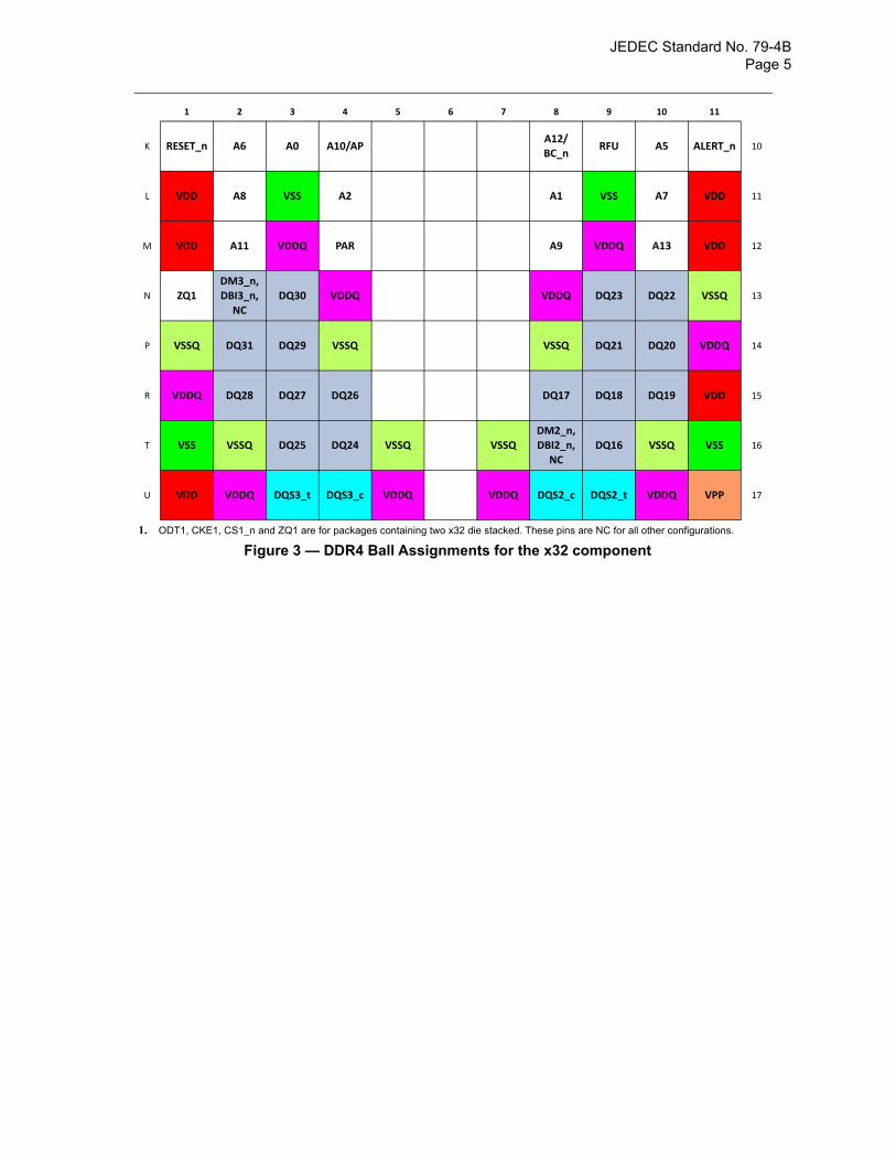
2.6 DDR4 SDRAM X32 Ballout using MO-XXXThe DDR4 SDRAM x32 component will have the pin assignments as defined in Figure 3. Blank cells are no ball locations.
1 2 3 4 5 6 7 8 9 10 11
A VPP VDDQ DQS0_t DQS0_c VDDQ VDDQ DQS1_c DQS1_t VDDQ VDD 1
B VSS VSSQ DQ0
DM0_n,
DBI0_n,
NC
VSSQ VSSQ DQ8 DQ9 VSSQ VSS 2
C VDD DQ3 DQ2 DQ1 DQ10 DQ11 DQ12 VDDQ 3
D VDDQ DQ4 DQ5 VSSQ VSSQ DQ13 DQ15 VSSQ 4
E VSSQ DQ6 DQ7 VDDQ VDDQ DQ14
DM1_n,
DBI1_n,
NC
ZQ 5
F VDD ODT1 VDDQ ODT CLK_t VDDQ CS1_n VDD 6
G VDD CKE1 VSS CKE CLK_c VSS TEN VDD 7
H VREFCA BA0 ACT_nWE_n/
A14CS_n
RAS_n/A16
BA1 RFU 8
J VSS A4 VSS BG0CAS_n/
A15VSS A3 VSS 9
1. ODT1, CKE1, CS1_n and ZQ1 are for packages containing two x32 die stacked. These pins are NC for all other configurations.
1 2 3 4 8 95 6 7ABCDEFGHJ
MO-207 Variation DY-z (x16)
N
10 11
PRTUVWY
AAAB
with support balls
1 2 3 4 8 95 6 7ABCDEFGHJKLMNPR
MO - 207 Variation DU-z (x16)
T
KLM
Populated ballBall not populated
JEDEC Standard No. 79-4B Page 5
Figure 3 — DDR4 Ball Assignments for the x32 component
K RESET_n A6 A0 A10/APA12/BC_n
RFU A5 ALERT_n 10
L VDD A8 VSS A2 A1 VSS A7 VDD 11
M VDD A11 VDDQ PAR A9 VDDQ A13 VDD 12
N ZQ1DM3_n, DBI3_n,
NC
DQ30 VDDQ VDDQ DQ23 DQ22 VSSQ 13
P VSSQ DQ31 DQ29 VSSQ VSSQ DQ21 DQ20 VDDQ 14
R VDDQ DQ28 DQ27 DQ26 DQ17 DQ18 DQ19 VDD 15
T VSS VSSQ DQ25 DQ24 VSSQ VSSQDM2_n, DBI2_n,
NC
DQ16 VSSQ VSS 16
U VDD VDDQ DQS3_t DQS3_c VDDQ VDDQ DQS2_c DQS2_t VDDQ VPP 17
1 2 3 4 5 6 7 8 9 10 11
1. ODT1, CKE1, CS1_n and ZQ1 are for packages containing two x32 die stacked. These pins are NC for all other configurations.
JEDEC Standard No. 79-4BPage 6
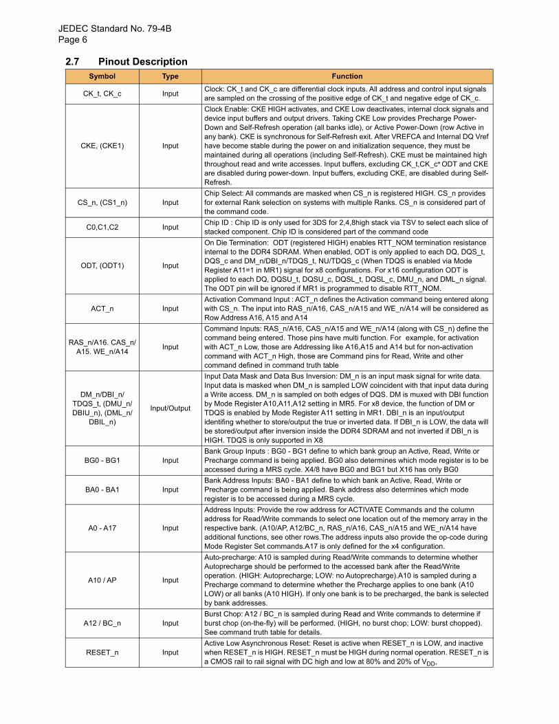
2.7 Pinout DescriptionSymbol Type Function
CK_t, CK_c InputClock: CK_t and CK_c are differential clock inputs. All address and control input signals are sampled on the crossing of the positive edge of CK_t and negative edge of CK_c.
CKE, (CKE1) Input
Clock Enable: CKE HIGH activates, and CKE Low deactivates, internal clock signals and device input buffers and output drivers. Taking CKE Low provides Precharge Power-Down and Self-Refresh operation (all banks idle), or Active Power-Down (row Active in any bank). CKE is synchronous for Self-Refresh exit. After VREFCA and Internal DQ Vref have become stable during the power on and initialization sequence, they must be maintained during all operations (including Self-Refresh). CKE must be maintained high throughout read and write accesses. Input buffers, excluding CK_t,CK_c, ODT and CKE are disabled during power-down. Input buffers, excluding CKE, are disabled during Self-Refresh.
CS_n, (CS1_n) InputChip Select: All commands are masked when CS_n is registered HIGH. CS_n provides for external Rank selection on systems with multiple Ranks. CS_n is considered part of the command code.
C0,C1,C2 InputChip ID : Chip ID is only used for 3DS for 2,4,8high stack via TSV to select each slice of stacked component. Chip ID is considered part of the command code
ODT, (ODT1) Input
On Die Termination: ODT (registered HIGH) enables RTT_NOM termination resistance internal to the DDR4 SDRAM. When enabled, ODT is only applied to each DQ, DQS_t, DQS_c and DM_n/DBI_n/TDQS_t, NU/TDQS_c (When TDQS is enabled via Mode Register A11=1 in MR1) signal for x8 configurations. For x16 configuration ODT is applied to each DQ, DQSU_t, DQSU_c, DQSL_t, DQSL_c, DMU_n, and DML_n signal. The ODT pin will be ignored if MR1 is programmed to disable RTT_NOM.
ACT_n InputActivation Command Input : ACT_n defines the Activation command being entered along with CS_n. The input into RAS_n/A16, CAS_n/A15 and WE_n/A14 will be considered as Row Address A16, A15 and A14
RAS_n/A16. CAS_n/A15. WE_n/A14
Input
Command Inputs: RAS_n/A16, CAS_n/A15 and WE_n/A14 (along with CS_n) define the command being entered. Those pins have multi function. For example, for activation with ACT_n Low, those are Addressing like A16,A15 and A14 but for non-activation command with ACT_n High, those are Command pins for Read, Write and other command defined in command truth table
DM_n/DBI_n/TDQS_t, (DMU_n/DBIU_n), (DML_n/
DBIL_n)
Input/Output
Input Data Mask and Data Bus Inversion: DM_n is an input mask signal for write data. Input data is masked when DM_n is sampled LOW coincident with that input data during a Write access. DM_n is sampled on both edges of DQS. DM is muxed with DBI function by Mode Register A10,A11,A12 setting in MR5. For x8 device, the function of DM or TDQS is enabled by Mode Register A11 setting in MR1. DBI_n is an input/output identifing whether to store/output the true or inverted data. If DBI_n is LOW, the data will be stored/output after inversion inside the DDR4 SDRAM and not inverted if DBI_n is HIGH. TDQS is only supported in X8
BG0 - BG1 InputBank Group Inputs : BG0 - BG1 define to which bank group an Active, Read, Write or Precharge command is being applied. BG0 also determines which mode register is to be accessed during a MRS cycle. X4/8 have BG0 and BG1 but X16 has only BG0
BA0 - BA1 InputBank Address Inputs: BA0 - BA1 define to which bank an Active, Read, Write or Precharge command is being applied. Bank address also determines which mode register is to be accessed during a MRS cycle.
A0 - A17 Input
Address Inputs: Provide the row address for ACTIVATE Commands and the column address for Read/Write commands to select one location out of the memory array in the respective bank. (A10/AP, A12/BC_n, RAS_n/A16, CAS_n/A15 and WE_n/A14 have additional functions, see other rows.The address inputs also provide the op-code during Mode Register Set commands.A17 is only defined for the x4 configuration.
A10 / AP Input
Auto-precharge: A10 is sampled during Read/Write commands to determine whether Autoprecharge should be performed to the accessed bank after the Read/Write operation. (HIGH: Autoprecharge; LOW: no Autoprecharge).A10 is sampled during a Precharge command to determine whether the Precharge applies to one bank (A10 LOW) or all banks (A10 HIGH). If only one bank is to be precharged, the bank is selected by bank addresses.
A12 / BC_n InputBurst Chop: A12 / BC_n is sampled during Read and Write commands to determine if burst chop (on-the-fly) will be performed. (HIGH, no burst chop; LOW: burst chopped). See command truth table for details.
RESET_n InputActive Low Asynchronous Reset: Reset is active when RESET_n is LOW, and inactive when RESET_n is HIGH. RESET_n must be HIGH during normal operation. RESET_n is a CMOS rail to rail signal with DC high and low at 80% and 20% of VDD,
JEDEC Standard No. 79-4B Page 7
2.8 DDR4 SDRAM Addressing
2.8.1 2 Gb Addressing Table
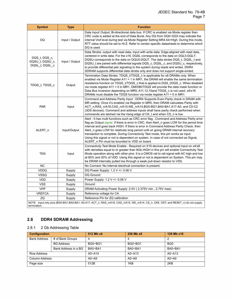
DQ Input / Output
Data Input/ Output: Bi-directional data bus. If CRC is enabled via Mode register then CRC code is added at the end of Data Burst. Any DQ from DQ0~DQ3 may indicate the internal Vref level during test via Mode Register Setting MR4 A4=High. During this mode, RTT value should be set to Hi-Z. Refer to vendor specific datasheets to determine which DQ is used.
DQS_t, DQS_c, DQSU_t, DQSU_c, DQSL_t, DQSL_c
Input / Output
Data Strobe: output with read data, input with write data. Edge-aligned with read data, centered in write data. For the x16, DQSL corresponds to the data on DQL0-DQL7; DQSU corresponds to the data on DQU0-DQU7. The data strobe DQS_t, DQSL_t and DQSU_t are paired with differential signals DQS_c, DQSL_c, and DQSU_c, respectively, to provide differential pair signaling to the system during reads and writes. DDR4 SDRAM supports differential data strobe only and does not support single-ended.
TDQS_t, TDQS_c Output
Termination Data Strobe: TDQS_t/TDQS_c is applicable for x8 DRAMs only. When enabled via Mode Register A11 = 1 in MR1, the DRAM will enable the same termination resistance function on TDQS_t/TDQS_c that is applied to DQS_t/DQS_c. When disabled via mode register A11 = 0 in MR1, DM/DBI/TDQS will provide the data mask function or Data Bus Inversion depending on MR5; A11,12,10and TDQS_c is not used. x4/x16 DRAMs must disable the TDQS function via mode register A11 = 0 in MR1.
PAR Input
Command and Address Parity Input : DDR4 Supports Even Parity check in DRAM with MR setting. Once it’s enabled via Register in MR5, then DRAM calculates Parity with ACT_n,RAS_n/A16,CAS_n/A15,WE_n/A14,BG0-BG1,BA0-BA1,A17-A0, and C0-C2 (3DS devices). Command and address inputs shall have parity check performed when commands are latched via the rising edge of CK_t and when CS_n is low.
ALERT_n Input/Output
Alert : It has multi functions such as CRC error flag , Command and Address Parity error flag as Output signal. If there is error in CRC, then Alert_n goes LOW for the period time interval and goes back HIGH. If there is error in Command Address Parity Check, then Alert_n goes LOW for relatively long period until on going DRAM internal recovery transaction to complete. During Connectivity Test mode, this pin works as input.Using this signal or not is dependent on system. In case of not connected as Signal, ALERT_n Pin must be bounded to VDD on board.
TEN Input
Connectivity Test Mode Enable : Required on X16 devices and optional input on x4/x8 with densities equal to or greater than 8Gb.HIGH in this pin will enable Connectivity Test Mode operation along with other pins. It is a CMOS rail to rail signal with AC high and low at 80% and 20% of VDD. Using this signal or not is dependent on System. This pin may be DRAM internally pulled low through a weak pull-down resistor to VSS.
NC No Connect: No internal electrical connection is present.
VDDQ Supply DQ Power Supply: 1.2 V +/- 0.06 V
VSSQ Supply DQ Ground
VDD Supply Power Supply: 1.2 V +/- 0.06 V
VSS Supply Ground
VPP Supply DRAM Activating Power Supply: 2.5V ( 2.375V min , 2.75V max)
VREFCA Supply Reference voltage for CA
ZQ Supply Reference Pin for ZQ calibration
NOTE Input only pins (BG0-BG1,BA0-BA1, A0-A17, ACT_n, RAS_n/A16, CAS_n/A15, WE_n/A14, CS_n, CKE, ODT, and RESET_n) do not supply termination.
Configuration 512 Mb x4 256 Mb x8 128 Mb x16
Bank Address # of Bank Groups 4 4 2
BG Address BG0~BG1 BG0~BG1 BG0
Bank Address in a BG BA0~BA1 BA0~BA1 BA0~BA1
Row Address A0~A14 A0~A13 A0~A13
Column Address A0~A9 A0~A9 A0~A9
Page size 512B 1KB 2KB
Symbol Type Function
JEDEC Standard No. 79-4BPage 8
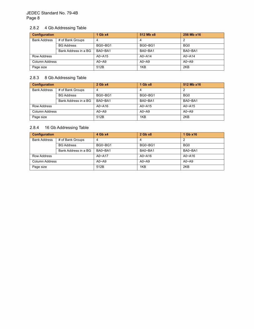
2.8.2 4 Gb Addressing Table
2.8.3 8 Gb Addressing Table
2.8.4 16 Gb Addressing Table
Configuration 1 Gb x4 512 Mb x8 256 Mb x16
Bank Address # of Bank Groups 4 4 2
BG Address BG0~BG1 BG0~BG1 BG0
Bank Address in a BG BA0~BA1 BA0~BA1 BA0~BA1
Row Address A0~A15 A0~A14 A0~A14
Column Address A0~A9 A0~A9 A0~A9
Page size 512B 1KB 2KB
Configuration 2 Gb x4 1 Gb x8 512 Mb x16
Bank Address # of Bank Groups 4 4 2
BG Address BG0~BG1 BG0~BG1 BG0
Bank Address in a BG BA0~BA1 BA0~BA1 BA0~BA1
Row Address A0~A16 A0~A15 A0~A15
Column Address A0~A9 A0~A9 A0~A9
Page size 512B 1KB 2KB
Configuration 4 Gb x4 2 Gb x8 1 Gb x16
Bank Address # of Bank Groups 4 4 2
BG Address BG0~BG1 BG0~BG1 BG0
Bank Address in a BG BA0~BA1 BA0~BA1 BA0~BA1
Row Address A0~A17 A0~A16 A0~A16
Column Address A0~A9 A0~A9 A0~A9
Page size 512B 1KB 2KB
JEDEC Standard No. 79-4B Page 9
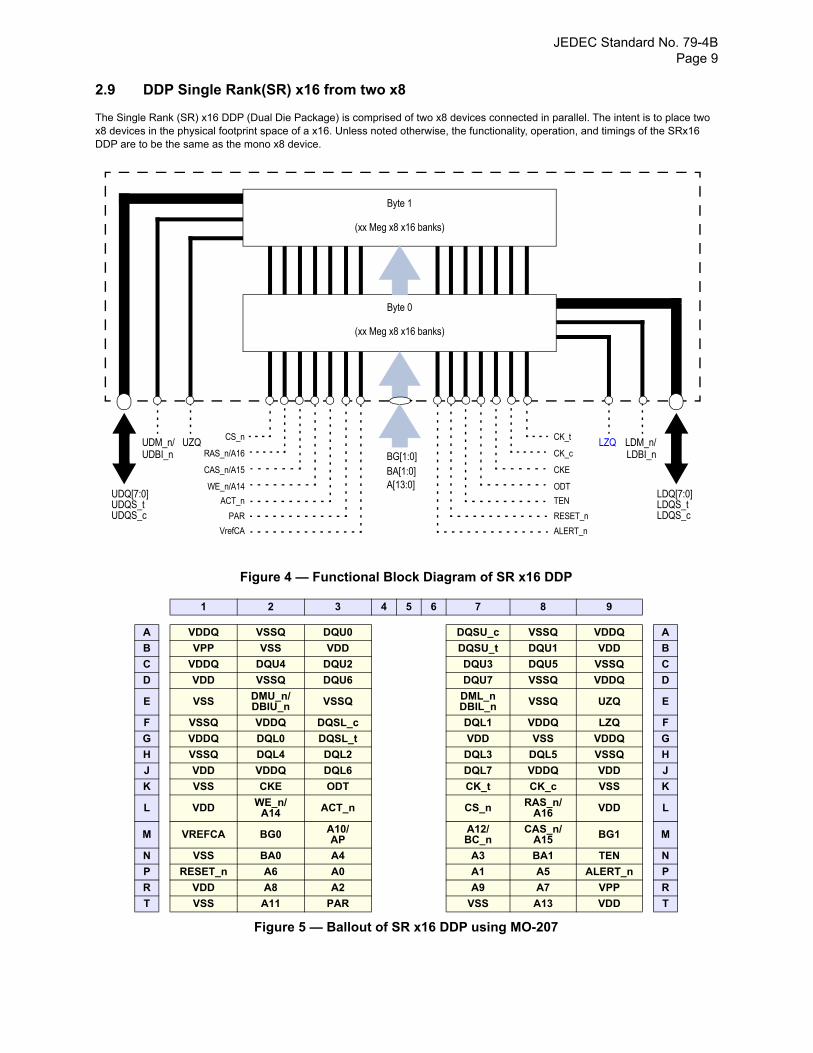
2.9 DDP Single Rank(SR) x16 from two x8
The Single Rank (SR) x16 DDP (Dual Die Package) is comprised of two x8 devices connected in parallel. The intent is to place two x8 devices in the physical footprint space of a x16. Unless noted otherwise, the functionality, operation, and timings of the SRx16 DDP are to be the same as the mono x8 device.
Figure 4 — Functional Block Diagram of SR x16 DDP
Figure 5 — Ballout of SR x16 DDP using MO-207
1 2 3 4 5 6 7 8 9
A VDDQ VSSQ DQU0 DQSU_c VSSQ VDDQ A
B VPP VSS VDD DQSU_t DQU1 VDD B
C VDDQ DQU4 DQU2 DQU3 DQU5 VSSQ C
D VDD VSSQ DQU6 DQU7 VSSQ VDDQ D
E VSS DMU_n/DBIU_n VSSQ DML_n
DBIL_n VSSQ UZQ E
F VSSQ VDDQ DQSL_c DQL1 VDDQ LZQ F
G VDDQ DQL0 DQSL_t VDD VSS VDDQ G
H VSSQ DQL4 DQL2 DQL3 DQL5 VSSQ H
J VDD VDDQ DQL6 DQL7 VDDQ VDD J
K VSS CKE ODT CK_t CK_c VSS K
L VDD WE_n/A14 ACT_n CS_n RAS_n/
A16 VDD L
M VREFCA BG0 A10/AP
A12/BC_n
CAS_n/A15 BG1 M
N VSS BA0 A4 A3 BA1 TEN N
P RESET_n A6 A0 A1 A5 ALERT_n P
R VDD A8 A2 A9 A7 VPP R
T VSS A11 PAR VSS A13 VDD T
Byte 1
(xx Meg x8 x16 banks)
Byte 0
(xx Meg x8 x16 banks)
BG[1:0]BG[1:0]BA[1:0]A[13:0]
UDM_n/UDBI_n
UZQCS_n
RAS_n/A16
CAS_n/A15
WE_n/A14
ACT_n
PAR
VrefCA
LDM_n/LDBI_n
LZQCK_t
CK_c
CKE
ODT
TEN
RESET_n
ALERT_n
UDQ[7:0]UDQS_tUDQS_c
LDQ[7:0]LDQS_tLDQS_c
JEDEC Standard No. 79-4BPage 10
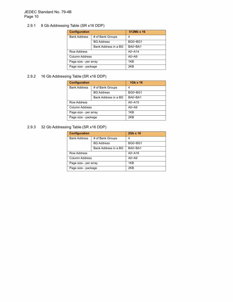
2.9.1 8 Gb Addressing Table (SR x16 DDP)
2.9.2 16 Gb Addressing Table (SR x16 DDP)
2.9.3 32 Gb Addressing Table (SR x16 DDP)
Configuration 512Mb x 16
Bank Address # of Bank Groups 4
BG Address BG0~BG1
Bank Address in a BG BA0~BA1
Row Address A0~A14
Column Address A0~A9
Page size - per array 1KB
Page size - package 2KB
Configuration 1Gb x 16
Bank Address # of Bank Groups 4
BG Address BG0~BG1
Bank Address in a BG BA0~BA1
Row Address A0~A15
Column Address A0~A9
Page size - per array 1KB
Page size - package 2KB
Configuration 2Gb x 16
Bank Address # of Bank Groups 4
BG Address BG0~BG1
Bank Address in a BG BA0~BA1
Row Address A0~A16
Column Address A0~A9
Page size - per array 1KB
Page size - package 2KB
JEDEC Standard No. 79-4B Page 11
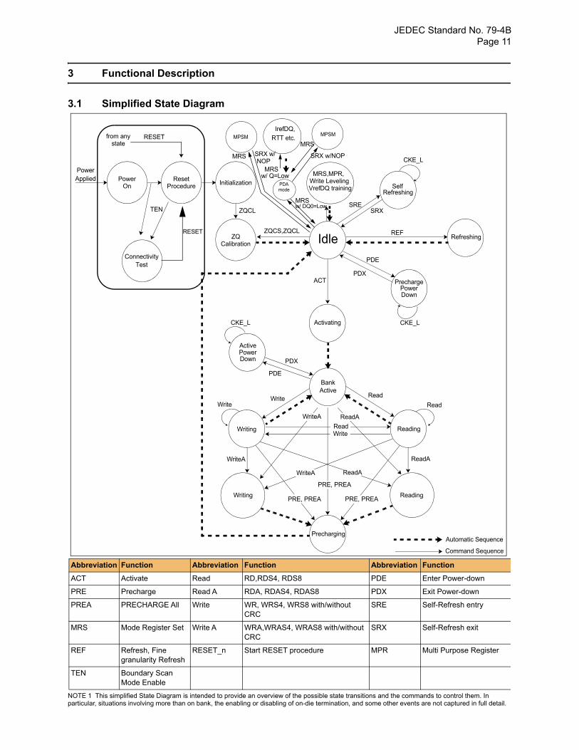
3 Functional Description
3.1 Simplified State Diagram
Self
IdleZQ
Bank
Precharging
Power
Writing
ACT
ReadA
Read
SRE
REF
PDE
PDX
PDX
PDE
Write
ReadAWriteA
Read
PRE, PREA
Refreshing
Refreshing
Down
PowerDown
Active
ReadA
Reading
WriteA
Active
Precharge
ReadingWriting
Activating
SRX
ReadWrite
Calibration
CKE_L
CKE_L CKE_L
PRE, PREA PRE, PREA
Write
WriteA
InitializationReset
ProcedurePower
On
PowerApplied
RESETfrom anystate
MRS,MPR,
MRS
Abbreviation Function Abbreviation Function Abbreviation Function
ACT Activate Read RD,RDS4, RDS8 PDE Enter Power-down
PRE Precharge Read A RDA, RDAS4, RDAS8 PDX Exit Power-down
PREA PRECHARGE All Write WR, WRS4, WRS8 with/without CRC
SRE Self-Refresh entry
MRS Mode Register Set Write A WRA,WRAS4, WRAS8 with/without CRC
SRX Self-Refresh exit
REF Refresh, Fine granularity Refresh
RESET_n Start RESET procedure MPR Multi Purpose Register
TEN Boundary Scan Mode Enable
MPSM
Connectivity
TEN
RESET
ZQCL
ZQCS,ZQCL
Automatic Sequence
Command Sequence
PDA
MPSM
mode
w/ DQ0=Low
MRS SRX w/NOP
MRS
MRS
SRX w/NOP
w/ Q=Low
Test
Write Leveling VrefDQ training
IrefDQ,RTT etc.
NOTE 1 This simplified State Diagram is intended to provide an overview of the possible state transitions and the commands to control them. In particular, situations involving more than on bank, the enabling or disabling of on-die termination, and some other events are not captured in full detail.
JEDEC Standard No. 79-4BPage 12
3.2 Basic Functionality The DDR4 SDRAM is a high-speed dynamic random-access memory internally configured as sixteen-banks, 4 bank group with 4 banks for each bank group for x4/x8 and eight-banks, 2 bank group with 4 banks for each bankgroup for x16 DRAM. The DDR4 SDRAM uses a 8n prefetch architecture to achieve high-speed operation. The 8n prefetch architecture is combined with an interface designed to transfer two data words per clock cycle at the I/O pins. A single read or write operation for the DDR4 SDRAM consists of a single 8n-bit wide, four clock data transfer at the internal DRAM core and eight corresponding n-bit wide, one-half clock cycle data transfers at the I/O pins.
Read and write operation to the DDR4 SDRAM are burst oriented, start at a selected location, and continue for a burst length of eight or a ‘chopped’ burst of four in a programmed sequence. Operation begins with the registration of an ACTIVATE Command, which is then followed by a Read or Write command. The address bits registered coincident with the ACTIVATE Command are used to select the bank and row to be activated (BG0-BG1 in x4/8 and BG0 in x16 select the bankgroup; BA0-BA1 select the bank; A0-A17 select the row; refer to “DDR4 SDRAM Addressing” on Section 2.8 for specific requirements). The address bits registered coincident with the Read or Write command are used to select the starting column location for the burst operation, determine if the auto precharge command is to be issued (via A10), and select BC4 or BL8 mode ‘on the fly’ (via A12) if enabled in the mode register.
Prior to normal operation, the DDR4 SDRAM must be powered up and initialized in a predefined manner.
The following sections provide detailed information covering device reset and initialization, register definition, command descriptions, and device operation.
3.3 RESET and Initialization Procedure For power-up and reset initialization, in order to prevent DRAM from functioning improperly default values for the following MR settings need to be defined.Gear down mode (MR3 A[3]) : 0 = 1/2 RatePer DRAM Addressability (MR3 A[4]) : 0 = DisableMax Power Saving Mode (MR4 A[1]) : 0 = DisableCS to Command/Address Latency (MR4 A[8:6]) : 000 = DisableCA Parity Latency Mode (MR5 A[2:0]) : 000 = DisableHard Post Package Repair mode (MR4 A[13]) : 0 = DisableSoft Post Package Repair mode (MR4 A[5]) : 0 = Disable
3.3.1 Power-up Initialization SequenceThe following sequence is required for POWER UP and Initialization and is shown in Figure 6. 1. Apply power (RESET_n and TEN are recommended to be maintained below 0.2 x VDD; all other inputs may be undefined). RESET_n needs to be maintained below 0.2 x VDD for minimum 200us with stable power and TEN needs to be maintained below 0.2 x VDD for minimum 700us with stable power. CKE is pulled “ Low” anytime before RESET_n being de-asserted (min. time 10ns) . The power voltage ramp time between 300mV to VDD min must be no greater than 200ms; and during the ramp, VDD ≥ VDDQ and
(VDD-VDDQ) < 0.3 V. VPP must ramp at the same time or earlier than VDD and VPP must be equal to or higher than VDD at all times.
• VDD and VDDQ are driven from a single power converter output, AND
• The voltage levels on all pins other than VDD,VDDQ,VSS,VSSQ must be less than or equal to VDDQ and VDD on
one side and must be larger than or equal to VSSQ and VSS on the other side. In addition, VTT is limited to 0.76 V max once power ramp is finished, AND
• VrefCA tracks VDD/2. or
• Apply VDD without any slope reversal before or at the same time as VDDQ
• Apply VDDQ without any slope reversal before or at the same time as VTT & VrefCA.
• Apply VPP without any slope reversal before or at the same time as VDD.• The voltage levels on all pins other than VDD,VDDQ,VSS,VSSQ must be less than or equal to VDDQ and VDD on
one side and must be larger than or equal to VSSQ and VSS on the other side.2. After RESET_n is de-asserted, wait for another 500us until CKE becomes active. During this time, the DRAM will start internal initialization; this will be done independently of external clocks.3. Clocks (CK_t,CK_c) need to be started and stabilized for at least 10ns or 5tCK (which is larger) before CKE goes active. Since CKE is a synchronous signal, the corresponding setup time to clock (tIS) must be met. Also a Deselect command must be registered (with tIS set up time to clock) at clock edge Td. Once the CKE registered “High” after Reset, CKE needs to be continuously registered “High” until the initialization sequence is finished, including expiration of tDLLK and tZQinit.4. The DDR4 SDRAM keeps its on-die termination in high-impedance state as long as RESET_n is asserted. Further, the SDRAM keeps its on-die termination in high impedance state after RESET_n deassertion until CKE is registered HIGH. The ODT input signal may be in undefined state until tIS before CKE is registered HIGH. When CKE is registered HIGH, the ODT input signal may be statically held at either LOW or HIGH. If RTT_NOM is to be enabled in MR1 the ODT input signal must be statically held LOW. In all cases, the ODT input signal remains static until the power up initialization sequence is finished, including the expiration of tDLLK and tZQinit.
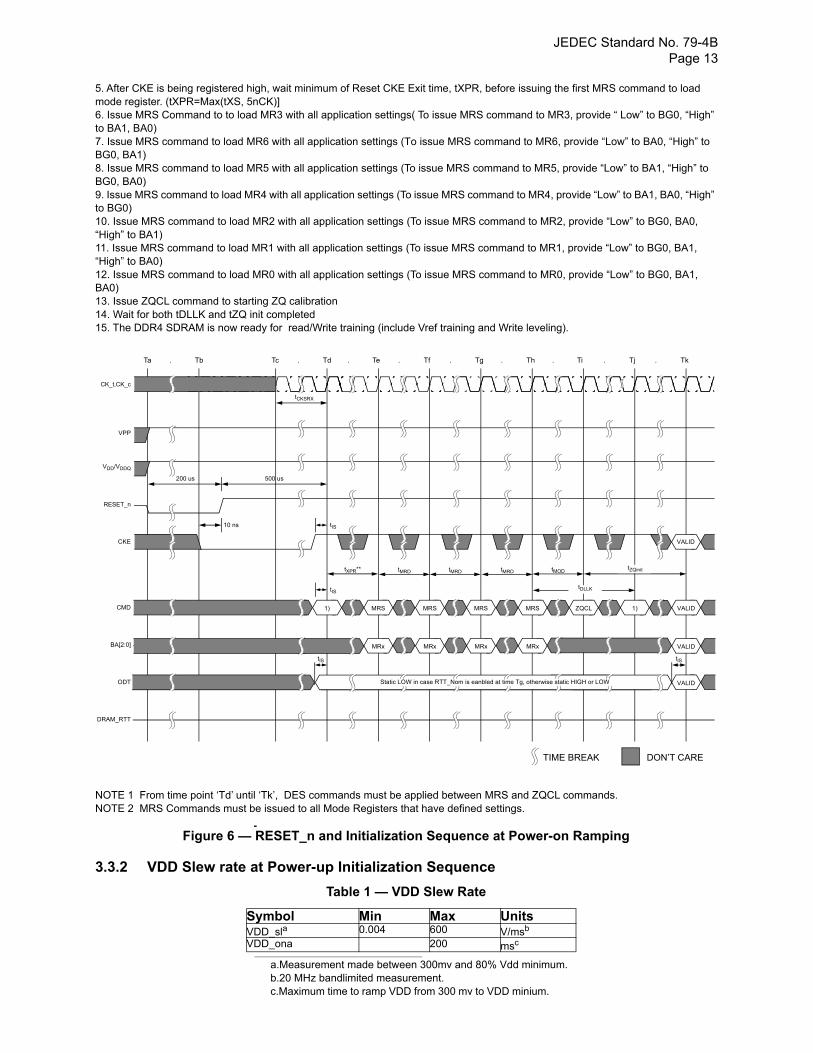
JEDEC Standard No. 79-4B Page 13
5. After CKE is being registered high, wait minimum of Reset CKE Exit time, tXPR, before issuing the first MRS command to load mode register. (tXPR=Max(tXS, 5nCK)]6. Issue MRS Command to to load MR3 with all application settings( To issue MRS command to MR3, provide “ Low” to BG0, “High” to BA1, BA0)7. Issue MRS command to load MR6 with all application settings (To issue MRS command to MR6, provide “Low” to BA0, “High” to BG0, BA1) 8. Issue MRS command to load MR5 with all application settings (To issue MRS command to MR5, provide “Low” to BA1, “High” to BG0, BA0) 9. Issue MRS command to load MR4 with all application settings (To issue MRS command to MR4, provide “Low” to BA1, BA0, “High” to BG0) 10. Issue MRS command to load MR2 with all application settings (To issue MRS command to MR2, provide “Low” to BG0, BA0, “High” to BA1) 11. Issue MRS command to load MR1 with all application settings (To issue MRS command to MR1, provide “Low” to BG0, BA1, “High” to BA0) 12. Issue MRS command to load MR0 with all application settings (To issue MRS command to MR0, provide “Low” to BG0, BA1, BA0) 13. Issue ZQCL command to starting ZQ calibration 14. Wait for both tDLLK and tZQ init completed15. The DDR4 SDRAM is now ready for read/Write training (include Vref training and Write leveling).
NOTE 1 From time point ‘Td’ until ‘Tk’, DES commands must be applied between MRS and ZQCL commands.NOTE 2 MRS Commands must be issued to all Mode Registers that have defined settings.
Figure 6 — RESET_n and Initialization Sequence at Power-on Ramping
3.3.2 VDD Slew rate at Power-up Initialization Sequence
Table 1 — VDD Slew Rate
Symbol Min Max UnitsVDD_sla
a.Measurement made between 300mv and 80% Vdd minimum.
0.004 600 V/msb
b.20 MHz bandlimited measurement.
VDD_ona 200 msc
c.Maximum time to ramp VDD from 300 mv to VDD minium.
VDD/VDDQ
CK_t,CK_c
RESET_n
Tc . Td . Te . Tf . . Th . Ti . Tj . TkTg
tCKSRX
Ta . Tb
CKE
200 us 500 us
10 ns tIS
1) MRS
MRx
MRS
MRx
MRS
MRx
MRS
MRx
ZQCL
tXPR**
tIS
tMRD tMRD tMRD tMOD
CMD
BA[2:0]
tIS
ODT
DRAM_RTT
tDLLK
Static LOW in case RTT_Nom is eanbled at time Tg, otherwise static HIGH or LOW
tZQinit
1) VALID
VALID
VALID
tIS
VPP
VALID
TIME BREAK DON’T CARE
JEDEC Standard No. 79-4BPage 14
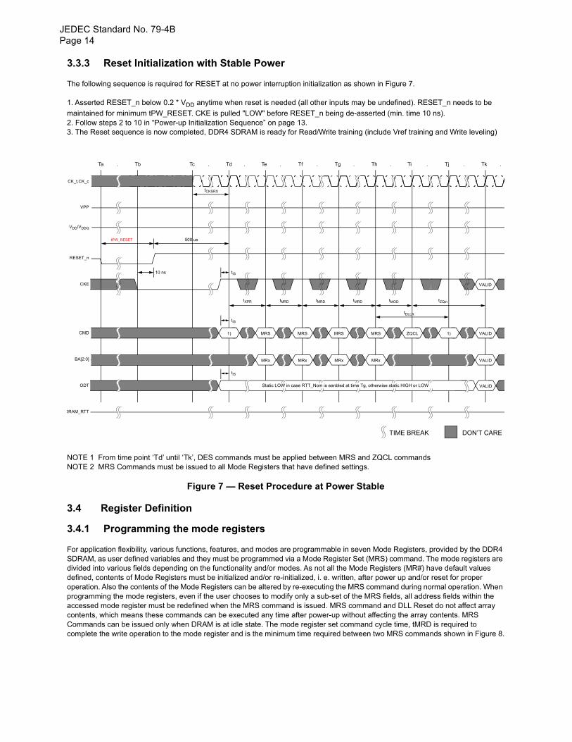
3.3.3 Reset Initialization with Stable Power
The following sequence is required for RESET at no power interruption initialization as shown in Figure 7.
1. Asserted RESET_n below 0.2 * VDD anytime when reset is needed (all other inputs may be undefined). RESET_n needs to be
maintained for minimum tPW_RESET. CKE is pulled "LOW" before RESET_n being de-asserted (min. time 10 ns).2. Follow steps 2 to 10 in “Power-up Initialization Sequence” on page 13.3. The Reset sequence is now completed, DDR4 SDRAM is ready for Read/Write training (include Vref training and Write leveling)
NOTE 1 From time point ‘Td’ until ‘Tk’, DES commands must be applied between MRS and ZQCL commandsNOTE 2 MRS Commands must be issued to all Mode Registers that have defined settings.
Figure 7 — Reset Procedure at Power Stable
3.4 Register Definition
3.4.1 Programming the mode registers
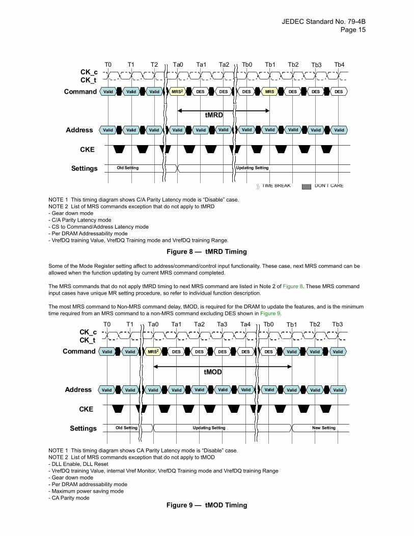
For application flexibility, various functions, features, and modes are programmable in seven Mode Registers, provided by the DDR4 SDRAM, as user defined variables and they must be programmed via a Mode Register Set (MRS) command. The mode registers are divided into various fields depending on the functionality and/or modes. As not all the Mode Registers (MR#) have default values defined, contents of Mode Registers must be initialized and/or re-initialized, i. e. written, after power up and/or reset for proper operation. Also the contents of the Mode Registers can be altered by re-executing the MRS command during normal operation. When programming the mode registers, even if the user chooses to modify only a sub-set of the MRS fields, all address fields within the accessed mode register must be redefined when the MRS command is issued. MRS command and DLL Reset do not affect array contents, which means these commands can be executed any time after power-up without affecting the array contents. MRS Commands can be issued only when DRAM is at idle state. The mode register set command cycle time, tMRD is required to complete the write operation to the mode register and is the minimum time required between two MRS commands shown in Figure 8.
VDD/VDDQ
CK_t,CK_c
RESET_n
Tc . Td . Te . Tf . . Th . Ti . Tj . Tk .TgTa . Tb
CKE
tPW_RESET 500 us
10 ns tIS
1) MRS
MRx
MRS
MRx
MRS
MRx
MRS
MRx
ZQCL
tXPR
tIS
tMRD tMRD tMRD
CMD
BA[2:0]
tIS
ODT
DRAM_RTT
tCKSRX
tMOD tZQin
tDLLK
Static LOW in case RTT_Nom is eanbled at time Tg, otherwise static HIGH or LOW
1) VALID
VALID
VALID
VPP
VALID
TIME BREAK DON’T CARE
JEDEC Standard No. 79-4B Page 15
NOTE 1 This timing diagram shows C/A Parity Latency mode is “Disable” case.NOTE 2 List of MRS commands exception that do not apply to tMRD- Gear down mode - C/A Parity Latency mode- CS to Command/Address Latency mode- Per DRAM Addressability mode- VrefDQ training Value, VrefDQ Training mode and VrefDQ training Range.
Figure 8 — tMRD Timing
Some of the Mode Register setting affect to address/command/control input functionality. These case, next MRS command can be allowed when the function updating by current MRS command completed.
The MRS commands that do not apply tMRD timing to next MRS command are listed in Note 2 of Figure 8. These MRS command input cases have unique MR setting procedure, so refer to individual function description.
The most MRS command to Non-MRS command delay, tMOD, is required for the DRAM to update the features, and is the minimum time required from an MRS command to a non-MRS command excluding DES shown in Figure 9.
NOTE 1 This timing diagram shows CA Parity Latency mode is “Disable” case.NOTE 2 List of MRS commands exception that do not apply to tMOD- DLL Enable, DLL Reset- VrefDQ training Value, internal Vref Monitor, VrefDQ Training mode and VrefDQ training Range- Gear down mode- Per DRAM addressability mode- Maximum power saving mode- CA Parity mode
Figure 9 — tMOD Timing
TIME BREAK DON’T CARE
T0 T1 Ta0 Ta1 Ta2 Tb0 Tb1 Tb2 Tb3
CK_tCK_c
MRS2 MRS
tMRD
Command
Valid Valid Valid Valid Valid Valid Valid Valid Valid ValidValidAddress
CKE
Valid Valid DES
Old Setting Updating SettingSettings
Tb4
Valid
T2
DES DES DES DES DES
Command
T0 T1 Ta0 Ta1 Ta2 Ta3 Ta4 Tb0 Tb1
CK_tCK_c
MRS2
tMOD
Valid Valid Valid Valid Valid Valid Valid Valid Valid Valid ValidAddress
CKE
Valid Valid DES
Old Setting Updating Setting New SettingSettings
Tb2 Tb3
Valid ValidValidDES DES DES DES
JEDEC Standard No. 79-4BPage 16
Some of the mode register setting cases, function updating takes longer than tMOD. The MRS commands that do not apply tMOD timing to next valid command excluding DES is listed in Note 2 of Figure 9. These MRS command input cases have unique MR
setting procedure, so refer to individual function description.
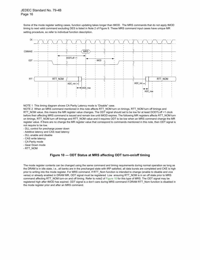
NOTE 1 This timing diagram shows CA Parity Latency mode is “Disable” case.NOTE 2 When an MRS command mentioned in this note affects RTT_NOM turn on timings, RTT_NOM turn off timings and RTT_NOM value, this means the MR register value changes. The ODT signal should set to be low for at least DODTLoff +1 clock before their affecting MRS command is issued and remain low until tMOD expires. The following MR registers affects RTT_NOM turn on timings, RTT_NOM turn off timings and RTT_NOM value and it requires ODT to be low when an MRS command change the MR register value. If there are no change the MR register value that correspond to commands mentioned in this note, then ODT signal is not require to be low.- DLL control for precharge power down- Additive latency and CAS read latency- DLL enable and disable- CAS write latency- CA Parity mode- Gear Down mode- RTT_NOM
Figure 10 — ODT Status at MRS affecting ODT turn-on/off timing
The mode register contents can be changed using the same command and timing requirements during normal operation as long as the DRAM is in idle state, i.e., all banks are in the precharged state with tRP satisfied, all data bursts are completed and CKE is high prior to writing into the mode register. For MRS command, If RTT_Nom function is intended to change (enable to disable and vice versa) or already enabled in DRAM MR, ODT signal must be registered Low ensuring RTT_NOM is in an off state prior to MRS command affecting RTT_NOM turn-on and off timing. Refer to note2 of Figure 10 for this type of MRS. The ODT signal may be registered high after tMOD has expired. ODT signal is a don’t care during MRS command if DRAM RTT_Nom function is disabled in the mode register prior and after an MRS command.
CK
COMMAND
ODTDODTLoff + 1
MRS
RTT
tMOD
tADC_min
tADC_max
tADC_min
tADC_max
RTT_NOM RTT_NOM
JEDEC Standard No. 79-4B Page 17
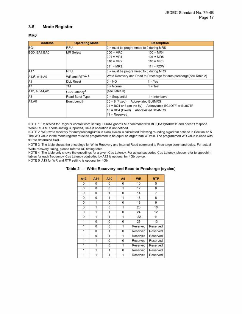
3.5 Mode Register
MR0
NOTE 1 Reserved for Register control word setting .DRAM ignores MR command with BG0,BA1;BA0=111 and doesn’t respond. When RFU MR code setting is inputted, DRAM operation is not defined.NOTE 2 WR (write recovery for autoprecharge)min in clock cycles is calculated following rounding algorithm defined in Section 13.5. The WR value in the mode register must be programmed to be equal or larger than WRmin. The programmed WR value is used with tRP to determine tDAL.
NOTE 3 The table shows the encodings for Write Recovery and internal Read command to Precharge command delay. For actual Write recovery timing, please refer to AC timing table.NOTE 4 The table only shows the encodings for a given Cas Latency. For actual supported Cas Latency, please refer to speedbin tables for each frequency. Cas Latency controlled by A12 is optional for 4Gb device.NOTE 5 A13 for WR and RTP setting is optional for 4Gb.
Table 2 — Write Recovery and Read to Precharge (cycles)
Address Operating Mode Description
BG1 RFU 0 = must be programmed to 0 during MRS
BG0, BA1:BA0 MR Select 000 = MR0 100 = MR4001 = MR1 101 = MR5010 = MR2 110 = MR6
011 = MR3 111 = RCW1
A17 RFU 0 = must be programmed to 0 during MRS
A135, A11:A9 WR and RTP2, 3 Write Recovery and Read to Precharge for auto precharge(see Table 2)
A8 DLL Reset 0 = NO 1 = Yes
A7 TM 0 = Normal 1 = Test
A12, A6:A4,A2 CAS Latency4 (see Table 3)
A3 Read Burst Type 0 = Sequential 1 = Interleave
A1:A0 Burst Length 00 = 8 (Fixed) Abbreviated BL8MRS01 = BC4 or 8 (on the fly) Abbreviated BC4OTF or BL8OTF10 = BC4 (Fixed) Abbreviated BC4MRS11 = Reserved
A13 A11 A10 A9 WR RTP
0 0 0 0 10 5
0 0 0 1 12 6
0 0 1 0 14 7
0 0 1 1 16 8
0 1 0 0 18 9
0 1 0 1 20 10
0 1 1 0 24 12
0 1 1 1 22 11
1 0 0 0 26 13
1 0 0 1 Reserved Reserved
1 0 1 0 Reserved Reserved
1 0 1 1 Reserved Reserved
1 1 0 0 Reserved Reserved
1 1 0 1 Reserved Reserved
1 1 1 0 Reserved Reserved
1 1 1 1 Reserved Reserved
JEDEC Standard No. 79-4BPage 18
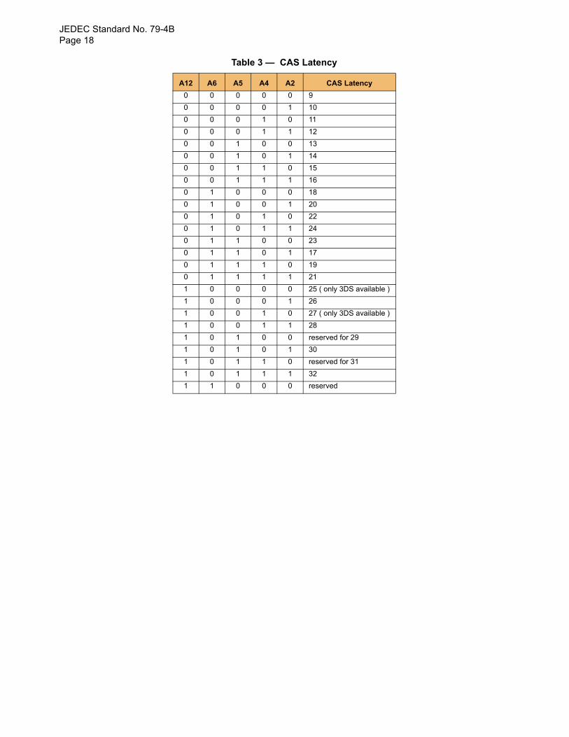
Table 3 — CAS Latency
A12 A6 A5 A4 A2 CAS Latency
0 0 0 0 0 9
0 0 0 0 1 10
0 0 0 1 0 11
0 0 0 1 1 12
0 0 1 0 0 13
0 0 1 0 1 14
0 0 1 1 0 15
0 0 1 1 1 16
0 1 0 0 0 18
0 1 0 0 1 20
0 1 0 1 0 22
0 1 0 1 1 24
0 1 1 0 0 23
0 1 1 0 1 17
0 1 1 1 0 19
0 1 1 1 1 21
1 0 0 0 0 25 ( only 3DS available )
1 0 0 0 1 26
1 0 0 1 0 27 ( only 3DS available )
1 0 0 1 1 28
1 0 1 0 0 reserved for 29
1 0 1 0 1 30
1 0 1 1 0 reserved for 31
1 0 1 1 1 32
1 1 0 0 0 reserved
JEDEC Standard No. 79-4B Page 19
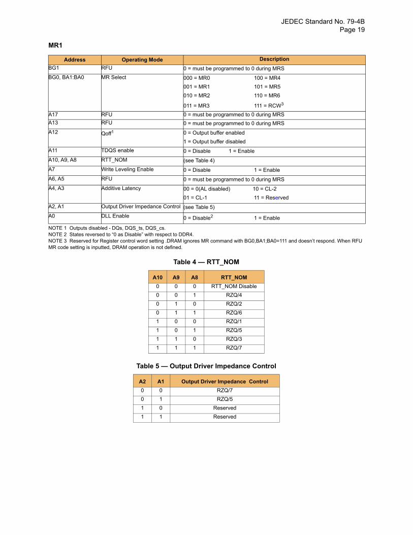
MR1
NOTE 1 Outputs disabled - DQs, DQS_ts, DQS_cs.NOTE 2 States reversed to “0 as Disable” with respect to DDR4.NOTE 3 Reserved for Register control word setting .DRAM ignores MR command with BG0,BA1;BA0=111 and doesn’t respond. When RFU MR code setting is inputted, DRAM operation is not defined.
Table 4 — RTT_NOM
Table 5 — Output Driver Impedance Control
Address Operating Mode Description
BG1 RFU 0 = must be programmed to 0 during MRS
BG0, BA1:BA0 MR Select 000 = MR0 100 = MR4
001 = MR1 101 = MR5
010 = MR2 110 = MR6
011 = MR3 111 = RCW3
A17 RFU 0 = must be programmed to 0 during MRS
A13 RFU 0 = must be programmed to 0 during MRS
A12 Qoff1 0 = Output buffer enabled
1 = Output buffer disabled
A11 TDQS enable 0 = Disable 1 = Enable
A10, A9, A8 RTT_NOM (see Table 4)
A7 Write Leveling Enable 0 = Disable 1 = Enable
A6, A5 RFU 0 = must be programmed to 0 during MRS
A4, A3 Additive Latency 00 = 0(AL disabled) 10 = CL-2
01 = CL-1 11 = Reserved
A2, A1 Output Driver Impedance Control (see Table 5)
A0 DLL Enable 0 = Disable2 1 = Enable
A10 A9 A8 RTT_NOM
0 0 0 RTT_NOM Disable
0 0 1 RZQ/4
0 1 0 RZQ/2
0 1 1 RZQ/6
1 0 0 RZQ/1
1 0 1 RZQ/5
1 1 0 RZQ/3
1 1 1 RZQ/7
A2 A1 Output Driver Impedance Control
0 0 RZQ/7
0 1 RZQ/5
1 0 Reserved
1 1 Reserved
JEDEC Standard No. 79-4BPage 20
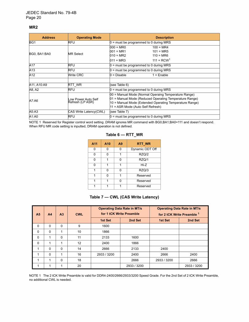
MR2
NOTE 1 Reserved for Register control word setting .DRAM ignores MR command with BG0,BA1;BA0=111 and doesn’t respond. When RFU MR code setting is inputted, DRAM operation is not defined.
Table 6 — RTT_WR
Table 7 — CWL (CAS Write Latency)
NOTE 1 The 2 tCK Write Preamble is valid for DDR4-2400/2666/2933/3200 Speed Grade. For the 2nd Set of 2 tCK Write Preamble, no additional CWL is needed.
Address Operating Mode Description
BG1 RFU 0 = must be programmed to 0 during MRS
BG0, BA1:BA0 MR Select
000 = MR0 100 = MR4001 = MR1 101 = MR5010 = MR2 110 = MR6
011 = MR3 111 = RCW1
A17 RFU 0 = must be programmed to 0 during MRS
A13 RFU 0 = must be programmed to 0 during MRS
A12 Write CRC 0 = Disable 1 = Enable
A11, A10:A9 RTT_WR (see Table 6)
A8, A2 RFU 0 = must be programmed to 0 during MRS
A7:A6 Low Power Auto Self Refresh (LP ASR)
00 = Manual Mode (Normal Operaing Temperature Range)01 = Manual Mode (Reduced Operating Temperature Range)10 = Manual Mode (Extended Operating Temperature Range)11 = ASR Mode (Auto Self Refresh)
A5:A3 CAS Write Latency(CWL) (see Table 7)
A1:A0 RFU 0 = must be programmed to 0 during MRS
A11 A10 A9 RTT_WR
0 0 0 Dynamic ODT Off
0 0 1 RZQ/2
0 1 0 RZQ/1
0 1 1 Hi-Z
1 0 0 RZQ/3
1 0 1 Reserved
1 1 0 Reserved
1 1 1 Reserved
A5 A4 A3 CWL
Operating Data Rate in MT/s
for 1 tCK Write Preamble
Operating Data Rate in MT/s
for 2 tCK Write Preamble 1
1st Set 2nd Set 1st Set 2nd Set
0 0 0 9 1600
0 0 1 10 1866
0 1 0 11 2133 1600
0 1 1 12 2400 1866
1 0 0 14 2666 2133 2400
1 0 1 16 2933 / 3200 2400 2666 2400
1 1 0 18 2666 2933 / 3200 2666
1 1 1 20 2933 / 3200 2933 / 3200
JEDEC Standard No. 79-4B Page 21
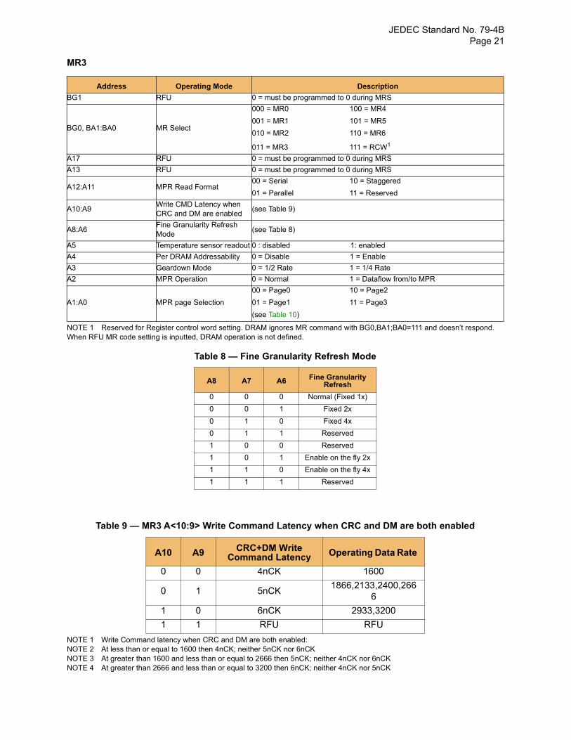
MR3
NOTE 1 Reserved for Register control word setting. DRAM ignores MR command with BG0,BA1;BA0=111 and doesn’t respond. When RFU MR code setting is inputted, DRAM operation is not defined.
Table 8 — Fine Granularity Refresh Mode
Table 9 — MR3 A<10:9> Write Command Latency when CRC and DM are both enabled
NOTE 1 Write Command latency when CRC and DM are both enabled:NOTE 2 At less than or equal to 1600 then 4nCK; neither 5nCK nor 6nCKNOTE 3 At greater than 1600 and less than or equal to 2666 then 5nCK; neither 4nCK nor 6nCKNOTE 4 At greater than 2666 and less than or equal to 3200 then 6nCK; neither 4nCK nor 5nCK
Address Operating Mode Description
BG1 RFU 0 = must be programmed to 0 during MRS
BG0, BA1:BA0 MR Select
000 = MR0 100 = MR4
001 = MR1 101 = MR5
010 = MR2 110 = MR6
011 = MR3 111 = RCW1
A17 RFU 0 = must be programmed to 0 during MRS
A13 RFU 0 = must be programmed to 0 during MRS
A12:A11 MPR Read Format00 = Serial 10 = Staggered
01 = Parallel 11 = Reserved
A10:A9Write CMD Latency when CRC and DM are enabled
(see Table 9)
A8:A6Fine Granularity Refresh Mode
(see Table 8)
A5 Temperature sensor readout 0 : disabled 1: enabled
A4 Per DRAM Addressability 0 = Disable 1 = Enable
A3 Geardown Mode 0 = 1/2 Rate 1 = 1/4 Rate
A2 MPR Operation 0 = Normal 1 = Dataflow from/to MPR
A1:A0 MPR page Selection
00 = Page0 10 = Page2
01 = Page1 11 = Page3
(see Table 10)
A8 A7 A6 Fine Granularity Refresh
0 0 0 Normal (Fixed 1x)
0 0 1 Fixed 2x
0 1 0 Fixed 4x
0 1 1 Reserved
1 0 0 Reserved
1 0 1 Enable on the fly 2x
1 1 0 Enable on the fly 4x
1 1 1 Reserved
A10 A9 CRC+DM Write Command Latency Operating Data Rate
0 0 4nCK 1600
0 1 5nCK1866,2133,2400,266
6
1 0 6nCK 2933,3200
1 1 RFU RFU
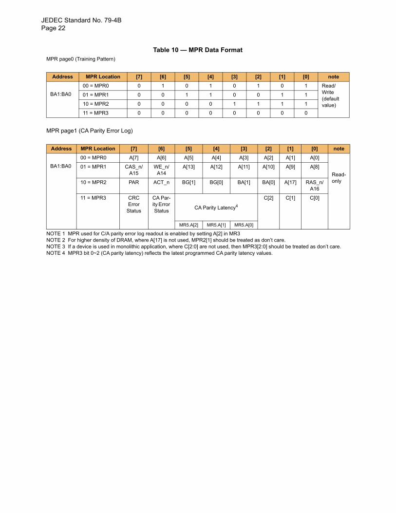
JEDEC Standard No. 79-4BPage 22
Table 10 — MPR Data FormatMPR page0 (Training Pattern)
MPR page1 (CA Parity Error Log)
NOTE 1 MPR used for C/A parity error log readout is enabled by setting A[2] in MR3NOTE 2 For higher density of DRAM, where A[17] is not used, MPR2[1] should be treated as don’t care.NOTE 3 If a device is used in monolithic application, where C[2:0] are not used, then MPR3[2:0] should be treated as don’t care.NOTE 4 MPR3 bit 0~2 (CA parity latency) reflects the latest programmed CA parity latency values.
Address MPR Location [7] [6] [5] [4] [3] [2] [1] [0] note
BA1:BA0
00 = MPR0 0 1 0 1 0 1 0 1 Read/Write (default value)
01 = MPR1 0 0 1 1 0 0 1 1
10 = MPR2 0 0 0 0 1 1 1 1
11 = MPR3 0 0 0 0 0 0 0 0
Address MPR Location [7] [6] [5] [4] [3] [2] [1] [0] note
BA1:BA0
00 = MPR0 A[7] A[6] A[5] A[4] A[3] A[2] A[1] A[0]
Read-only
01 = MPR1 CAS_n/A15
WE_n/A14
A[13] A[12] A[11] A[10] A[9] A[8]
10 = MPR2 PAR ACT_n BG[1] BG[0] BA[1] BA[0] A[17] RAS_n/A16
11 = MPR3 CRC Error
Status
CA Par-ity Error Status
CA Parity Latency4
C[2] C[1] C[0]
MR5.A[2] MR5.A[1] MR5.A[0]
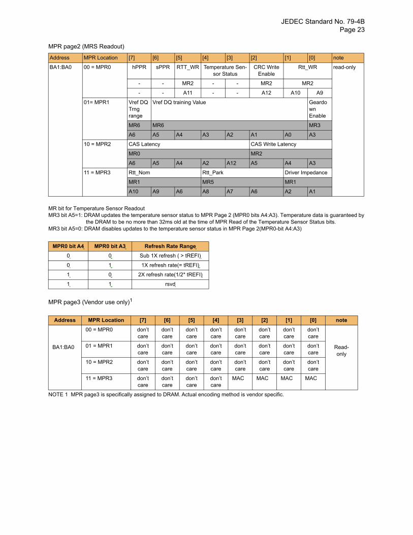
JEDEC Standard No. 79-4B Page 23
MPR page2 (MRS Readout)
MR bit for Temperature Sensor ReadoutMR3 bit A5=1: DRAM updates the temperature sensor status to MPR Page 2 (MPR0 bits A4:A3). Temperature data is guaranteed by the DRAM to be no more than 32ms old at the time of MPR Read of the Temperature Sensor Status bits.MR3 bit A5=0: DRAM disables updates to the temperature sensor status in MPR Page 2(MPR0-bit A4:A3)
MPR page3 (Vendor use only)1
NOTE 1 MPR page3 is specifically assigned to DRAM. Actual encoding method is vendor specific.
Address MPR Location [7] [6] [5] [4] [3] [2] [1] [0] note
BA1:BA0 00 = MPR0 hPPR sPPR RTT_WR Temperature Sen-sor Status
CRC Write Enable
Rtt_WR read-only
- - MR2 - - MR2 MR2
- - A11 - - A12 A10 A9
01= MPR1 Vref DQ Trng range
Vref DQ training Value Geardown Enable
MR6 MR6 MR3
A6 A5 A4 A3 A2 A1 A0 A3
10 = MPR2 CAS Latency CAS Write Latency
MR0 MR2
A6 A5 A4 A2 A12 A5 A4 A3
11 = MPR3 Rtt_Nom Rtt_Park Driver Impedance
MR1 MR5 MR1
A10 A9 A6 A8 A7 A6 A2 A1
MPR0 bit A4 MPR0 bit A3 Refresh Rate Range
0 0 Sub 1X refresh ( > tREFI)
0 1 1X refresh rate(= tREFI)
1 0 2X refresh rate(1/2* tREFI)
1 1 rsvd
Address MPR Location [7] [6] [5] [4] [3] [2] [1] [0] note
BA1:BA0
00 = MPR0 don’t care
don’t care
don’t care
don’t care
don’t care
don’t care
don’t care
don’t care
Read-only
01 = MPR1 don’t care
don’t care
don’t care
don’t care
don’t care
don’t care
don’t care
don’t care
10 = MPR2 don’t care
don’t care
don’t care
don’t care
don’t care
don’t care
don’t care
don’t care
11 = MPR3 don’t care
don’t care
don’t care
don’t care
MAC MAC MAC MAC
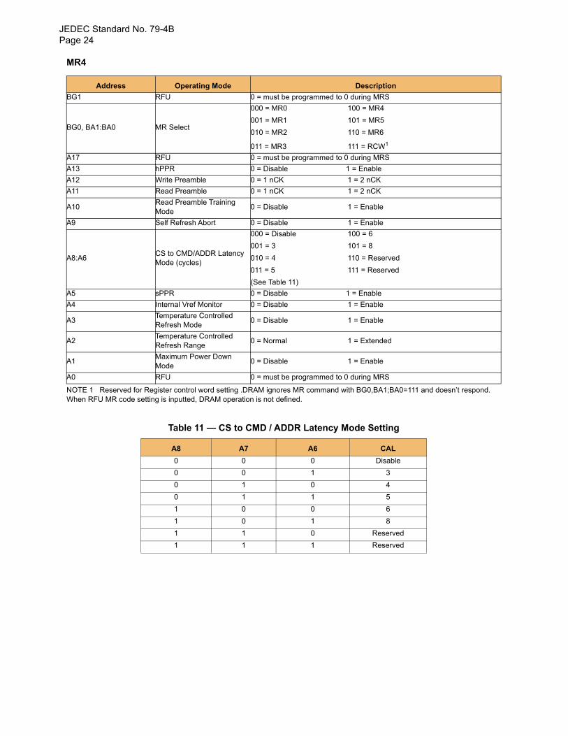
JEDEC Standard No. 79-4BPage 24
MR4
NOTE 1 Reserved for Register control word setting .DRAM ignores MR command with BG0,BA1;BA0=111 and doesn’t respond. When RFU MR code setting is inputted, DRAM operation is not defined.
Table 11 — CS to CMD / ADDR Latency Mode Setting
Address Operating Mode Description
BG1 RFU 0 = must be programmed to 0 during MRS
BG0, BA1:BA0 MR Select
000 = MR0 100 = MR4
001 = MR1 101 = MR5
010 = MR2 110 = MR6
011 = MR3 111 = RCW1
A17 RFU 0 = must be programmed to 0 during MRS
A13 hPPR 0 = Disable 1 = Enable
A12 Write Preamble 0 = 1 nCK 1 = 2 nCK
A11 Read Preamble 0 = 1 nCK 1 = 2 nCK
A10Read Preamble Training Mode
0 = Disable 1 = Enable
A9 Self Refresh Abort 0 = Disable 1 = Enable
A8:A6CS to CMD/ADDR Latency Mode (cycles)
000 = Disable 100 = 6
001 = 3 101 = 8
010 = 4 110 = Reserved
011 = 5 111 = Reserved
(See Table 11)
A5 sPPR 0 = Disable 1 = Enable
A4 Internal Vref Monitor 0 = Disable 1 = Enable
A3Temperature Controlled Refresh Mode
0 = Disable 1 = Enable
A2Temperature Controlled Refresh Range
0 = Normal 1 = Extended
A1Maximum Power Down Mode
0 = Disable 1 = Enable
A0 RFU 0 = must be programmed to 0 during MRS
A8 A7 A6 CAL
0 0 0 Disable
0 0 1 3
0 1 0 4
0 1 1 5
1 0 0 6
1 0 1 8
1 1 0 Reserved
1 1 1 Reserved
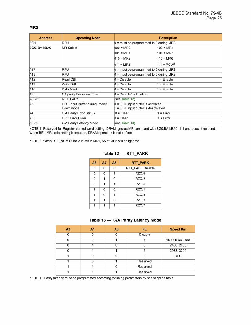
JEDEC Standard No. 79-4B Page 25
MR5
NOTE 1 Reserved for Register control word setting .DRAM ignores MR command with BG0,BA1;BA0=111 and doesn’t respond. When RFU MR code setting is inputted, DRAM operation is not defined.
NOTE 2 When RTT_NOM Disable is set in MR1, A5 of MR5 will be ignored.
Table 12 — RTT_PARK
Table 13 — C/A Parity Latency Mode
NOTE 1 Parity latency must be programmed according to timing parameters by speed grade table
Address Operating Mode Description
BG1 RFU 0 = must be programmed to 0 during MRS
BG0, BA1:BA0 MR Select 000 = MR0 100 = MR4
001 = MR1 101 = MR5
010 = MR2 110 = MR6
011 = MR3 111 = RCW1
A17 RFU 0 = must be programmed to 0 during MRS
A13 RFU 0 = must be programmed to 0 during MRS
A12 Read DBI 0 = Disable 1 = Enable
A11 Write DBI 0 = Disable 1 = Enable
A10 Data Mask 0 = Disable 1 = Enable
A9 CA parity Persistent Error 0 = Disable1 = Enable
A8:A6 RTT_PARK (see Table 12)
A5 ODT Input Buffer during Power Down mode
0 = ODT input buffer is activated 1 = ODT input buffer is deactivated
A4 C/A Parity Error Status 0 = Clear 1 = Error
A3 CRC Error Clear 0 = Clear 1 = Error
A2:A0 C/A Parity Latency Mode (see Table 13)
A8 A7 A6 RTT_PARK
0 0 0 RTT_PARK Disable
0 0 1 RZQ/4
0 1 0 RZQ/2
0 1 1 RZQ/6
1 0 0 RZQ/1
1 0 1 RZQ/5
1 1 0 RZQ/3
1 1 1 RZQ/7
A2 A1 A0 PL Speed Bin
0 0 0 Disable
0 0 1 4 1600,1866,2133
0 1 0 5 2400, 2666
0 1 1 6 2933, 3200
1 0 0 8 RFU
1 0 1 Reserved
1 1 0 Reserved
1 1 1 Reserved
JEDEC Standard No. 79-4BPage 26
MR6
NOTE 1 Reserved for Register control word setting . DRAM ignores MR command with BG0,BA1;BA0=111 and doesn’t respond.
Table 14 — tCCD_L and tDLLK
NOTE 1 tCCD_L/tDLLK should be programmed according to the value defined in AC parameter table per operating frequency
Table 15 — VrefDQ Training: Range
Address Operating Mode Description
BG1 RFU 0 = must be programmed to 0 during MRS
BG0, BA1:BA0 MR Select 000 = MR0 100 = MR4
001 = MR1 101 = MR5
010 = MR2 110 = MR6
011 = MR3 111 = RCW1
A17 RFU 0 = must be programmed to 0 during MRS
A13 RFU 0 = must be programmed to 0 during MRS
A12:A10 tCCD_L (see Table 14)
A9, A8 RFU 0 = must be programmed to 0 during MRS
A7 VrefDQ Training Enable 0 = Disable(Normal operation Mode) 1 = Enable(Training Mode)
A6 VrefDQ Training Range (see Table 15)
A5:A0 VrefDQ Training Value (see Table 16)
A12 A11 A10 tCCD_L.min (nCK)1 tDLLKmin (nCK)1 Note
0 0 0 4
597
Data rate 1333Mbps
0 0 1 51333Mbps < Data rate 1866Mbps
(1600/1866Mbps)
0 1 0 6 7681866Mbps < Data rate 2400Mbps
(2133/2400Mbps)
0 1 1 71024
TBD
1 0 0 8 TBD
1 0 1
Reserved1 1 0
1 1 1
A6 VrefDQ Range
0 Range 1
1 Range 2
JEDEC Standard No. 79-4B Page 27
Table 16 — VrefDQ Training: Values
MR7 DRAM: Ignore
The DDR4 SDRAM shall ignore any access to MR7 for all DDR4 SDRAM.Any bit setting within MR7 may not take any effect in the DDR4 SDRAM.
A5:A0 Range1 Range2 A5:A0 Range1 Range2
00 0000 60.00% 45.00% 01 1010 76.90% 61.90%
00 0001 60.65% 45.65% 01 1011 77.55% 62.55%
00 0010 61.30% 46.30% 01 1100 78.20% 63.20%
00 0011 61.95% 46.95% 01 1101 78.85% 63.85%
00 0100 62.60% 47.60% 01 1110 79.50% 64.50%
00 0101 63.25% 48.25% 01 1111 80.15% 65.15%
00 0110 63.90% 48.90% 10 0000 80.80% 65.80%
00 0111 64.55% 49.55% 10 0001 81.45% 66.45%
00 1000 65.20% 50.20% 10 0010 82.10% 67.10%
00 1001 65.85% 50.85% 10 0011 82.75% 67.75%
00 1010 66.50% 51.50% 10 0100 83.40% 68.40%
00 1011 67.15% 52.15% 10 0101 84.05% 69.05%
00 1100 67.80% 52.80% 10 0110 84.70% 69.70%
00 1101 68.45% 53.45% 10 0111 85.35% 70.35%
00 1110 69.10% 54.10% 10 1000 86.00% 71.00%
00 1111 69.75% 54.75% 10 1001 86.65% 71.65%
01 0000 70.40% 55.40% 10 1010 87.30% 72.30%
01 0001 71.05% 56.05% 10 1011 87.95% 72.95%
01 0010 71.70% 56.70% 10 1100 88.60% 73.60%
01 0011 72.35% 57.35% 10 1101 89.25% 74.25%
01 0100 73.00% 58.00% 10 1110 89.90% 74.90%
01 0101 73.65% 58.65% 10 1111 90.55% 75.55%
01 0110 74.30% 59.30% 11 0000 91.20% 76.20%
01 0111 74.95% 59.95% 11 0001 91.85% 76.85%
01 1000 75.60% 60.60% 11 0010 92.50% 77.50%
01 1001 76.25% 61.25% 11 0011 to 11 1111 Reserved Reserved
JEDEC Standard No. 79-4BPage 28
TE
2
9
,9,0
0
4 DDR4 SDRAM Command Description and Operation
4.1 Command Truth Table (a) Note 1,2,3 and 4 apply to the entire Command truth table.(b) Note 5 applies to all Read/Write commands.[BG=Bank Group Address, BA=Bank Address, RA=Row Address, CA=Column Address, BC_n=Burst Chop, X=Don’t Care, V=Valid].
Table 17 — Command Truth Table
NOTE 1 All DDR4 SDRAM commands are defined by states of CS_n, ACT_n, RAS_n/A16, CAS_n/A15, WE_n/A14 and CKE at the rising edge of the clock. The MSB of BG, BA, RA and CA are device density and configuration dependent. When ACT_n = H; pins RAS_n/A16, CAS_n/A15, and WE_n/A14 are used as command pins RAS_n, CAS_n, and WE_n respectively. When ACT_n = L; pins RAS_n/A16, CAS_n/A15, and WE_n/A14 are used as address pins A16, A15, and A14 respectivelyNOTE 2 RESET_n is Low enable command which will be used only for asynchronous reset so must be maintained HIGH during any function.NOTE 3 Bank Group addresses (BG) and Bank addresses (BA) determine which bank within a bank group to be operated upon. For MRS commands the BG and BA selects the specific Mode Register location.NOTE 4 “V” means “H or L (but a defined logic level)” and “X” means either “defined or undefined (like floating) logic level”.NOTE 5 Burst reads or writes cannot be terminated or interrupted and Fixed/on-the-Fly BL will be defined by MRS.NOTE 6 The Power Down Mode does not perform any refresh operation.NOTE 7 The state of ODT does not affect the states described Table 17. The ODT function is not available during Self Refresh.NOTE 8 Controller guarantees self refresh exit to be synchronous.NOTE 9 VPP and VREF(VrefCA) must be maintained during Self Refresh operation. NOTE 10 The No Operation command should be used in cases when the DDR4 SDRAM is in Gear Down Mode and Max Power Saving Mode Exit NOTE 11 Refer to the CKE Truth Table for more detail with CKE transition.NOTE 12 During a MRS command A17 is Reserved for Future Use and is device density and configuration dependent.
Function A
bb
rev
iati
on CKE CS_n ACT
_nRAS_n/A16
CAS_n/A15
WE_n/
A14
BG0-BG1
BA0-BA1
C2-C0
A12/BC_n
A17, A13, A11
A10/AP
A0-A9
NOPrevious
CycleCurrent Cycle
Mode Register Set MRS H H L H L L L BG BA V OP Code 1
Refresh REF H H L H L L H V V V V V V V
Self Refresh Entry SRE H L L H L L H V V V V V V V 7,
Self Refresh Exit SRX L H H X X X X X X X X X X X 7,81L H H H H V V V V V V V
Single Bank Precharge PRE H H L H L H L BG BA V V V L V
Precharge all Banks PREA H H L H L H L V V V V V H V
RFU RFU H H L H L H H RFU
Bank Activate ACT H H L L Row Address(RA)
BG BA V Row Address (RA)
Write (Fixed BL8 or BC4) WR H H L H H L L BG BA V V V L CA
Write (BC4, on the Fly) WRS4 H H L H H L L BG BA V L V L CA
Write (BL8, on the Fly) WRS8 H H L H H L L BG BA V H V L CA
Write with Auto Precharge(Fixed BL8 or BC4)
WRA H H L H H L L BG BA V V V H CA
Write with Auto Precharge(BC4, on the Fly)
WRAS4 H H L H H L L BG BA V L V H CA
Write with Auto Precharge(BL8, on the Fly)
WRAS8 H H L H H L L BG BA V H V H CA
Read (Fixed BL8 or BC4) RD H H L H H L H BG BA V V V L CA
Read (BC4, on the Fly) RDS4 H H L H H L H BG BA V L V L CA
Read (BL8, on the Fly) RDS8 H H L H H L H BG BA V H V L CA
Read with Auto Precharge (Fixed BL8 or BC4)
RDA H H L H H L H BG BA V V V H CA
Read with Auto Precharge(BC4, on the Fly)
RDAS4 H H L H H L H BG BA V L V H CA
Read with Auto Precharge(BL8, on the Fly)
RDAS8 H H L H H L H BG BA V H V H CA
No Operation NOP H H L H H H H V V V V V V V 1
Device Deselected DES H H H X X X X X X X X X X X
Power Down Entry PDE H L H X X X X X X X X X X X 6Power Down Exit PDX L H H X X X X X X X X X X X 6
ZQ calibration Long ZQCL H H L H H H L V V V V V H V
ZQ calibration Short ZQCS H H L H H H L V V V V V L V
JEDEC Standard No. 79-4B Page 29
4.2 CKE Truth Table
Table 18 — CKE Truth Table
NOTE 1 CKE (N) is the logic state of CKE at clock edge N; CKE (N-1) was the state of CKE at the previous clock edge.
NOTE 2 Current state is defined as the state of the DDR4 SDRAM immediately prior to clock edge N.
NOTE 3 COMMAND (N) is the command registered at clock edge N, and ACTION (N) is a result of COMMAND (N),ODT is not included here.
NOTE 4 All states and sequences not shown are illegal or reserved unless explicitly described elsewhere in this document.
NOTE 5 The state of ODT does not affect the states described Table 18. The ODT function is not available during Self-Refresh.
NOTE 6 During any CKE transition (registration of CKE H->L or CKE L->H), the CKE level must be maintained until 1nCK prior to tCKEmin being satisfied (at which time CKE may transition again).
NOTE 7 DESELECT and NOP are defined in the Table 17, Command Truth Table.
NOTE 8 On Self-Refresh Exit DESELECT commands must be issued on every clock edge occurring during the tXS period. Read or ODT commands may be issued only after tXSDLL is satisfied.
NOTE 9 Self-Refresh mode can only be entered from the All Banks Idle state.
NOTE 10 Must be a legal command as defined in the Command Truth Table.
NOTE 11 Valid commands for Power-Down Entry and Exit are DESELECT only.
NOTE 12 Valid commands for Self-Refresh Exit are DESELECT only except for Gear Down mode and Max Power Saving exit. NOP is allowed for these 2 modes.
NOTE 13 Self-Refresh can not be entered during Read or Write operations. For a detailed list of restrictions See “Self-Refresh Operation” on Section 4.27 and See “Power-Down Modes” on Section 4.28.
NOTE 14 The Power-Down does not perform any refresh operations.
NOTE 15 “X” means “don’t care“ (including floating around VREF) in Self-Refresh and Power-Down. It also applies to Address pins.
NOTE 16 VPP and VREF(VrefCA) must be maintained during Self-Refresh operation.
NOTE 17 If all banks are closed at the conclusion of the read, write or precharge command, then Precharge Power-Down is entered, otherwise Active Power-Down is entered.
NOTE 18 ‘Idle state’ is defined as all banks are closed (tRP, tDAL, etc. satisfied), no data bursts are in progress, CKE is high, and all timings from previous operations are satisfied (tMRD, tMOD, tRFC, tZQinit, tZQoper, tZQCS, etc.) as well as all Self-Refresh exit and Power-Down Exit parameters are satisfied (tXS, tXP,etc)
Current State2 CKE Command (N)3
RAS_n, CAS_n,WE_n, CS_n
Action (N)3 NOTE
Previous
Cycle1 (N-1)Current Cycle1
(N)
Power Down L L X Maintain Power-Down 14, 15
L H DESELECT Power Down Exit 11, 14
Self Refresh L L X Maintain Self Refresh 15, 16
L H DESELECT Self Refresh Exit 8, 12, 16
Bank(s) Active H L DESELECT Active Power Down Entry 11, 13, 14
Reading H L DESELECT Power Down Entry 11, 13, 14, 17
Writing H L DESELECT Power Down Entry 11, 13, 14, 17
Precharging H L DESELECT Power Down Entry 11, 13, 14, 17
Refreshing H L DESELECT Precharge Power Down Entry 11
All Banks Idle H L DESELECT Precharge Power Down Entry 11,13, 14, 18
H L REFRESH Self Refresh Entry 9, 13, 18
For more details with all signals See “Command Truth Table”. 10
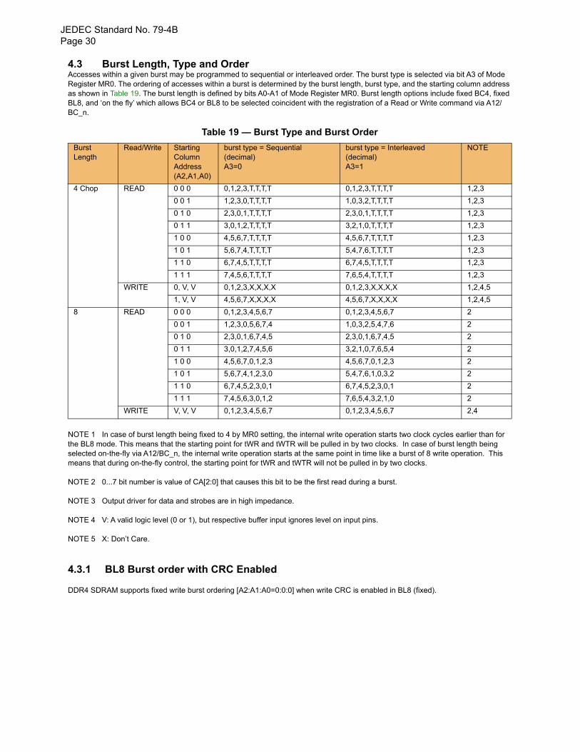
JEDEC Standard No. 79-4BPage 30
4.3 Burst Length, Type and Order Accesses within a given burst may be programmed to sequential or interleaved order. The burst type is selected via bit A3 of Mode Register MR0. The ordering of accesses within a burst is determined by the burst length, burst type, and the starting column address as shown in Table 19. The burst length is defined by bits A0-A1 of Mode Register MR0. Burst length options include fixed BC4, fixed BL8, and ‘on the fly’ which allows BC4 or BL8 to be selected coincident with the registration of a Read or Write command via A12/BC_n.
Table 19 — Burst Type and Burst Order
NOTE 1 In case of burst length being fixed to 4 by MR0 setting, the internal write operation starts two clock cycles earlier than for the BL8 mode. This means that the starting point for tWR and tWTR will be pulled in by two clocks. In case of burst length being selected on-the-fly via A12/BC_n, the internal write operation starts at the same point in time like a burst of 8 write operation. This means that during on-the-fly control, the starting point for tWR and tWTR will not be pulled in by two clocks.
NOTE 2 0...7 bit number is value of CA[2:0] that causes this bit to be the first read during a burst.
NOTE 3 Output driver for data and strobes are in high impedance.
NOTE 4 V: A valid logic level (0 or 1), but respective buffer input ignores level on input pins.
NOTE 5 X: Don’t Care.
4.3.1 BL8 Burst order with CRC Enabled
DDR4 SDRAM supports fixed write burst ordering [A2:A1:A0=0:0:0] when write CRC is enabled in BL8 (fixed).
Burst Length
Read/Write Starting ColumnAddress(A2,A1,A0)
burst type = Sequential(decimal)A3=0
burst type = Interleaved(decimal)A3=1
NOTE
4 Chop READ 0 0 0 0,1,2,3,T,T,T,T 0,1,2,3,T,T,T,T 1,2,3
0 0 1 1,2,3,0,T,T,T,T 1,0,3,2,T,T,T,T 1,2,3
0 1 0 2,3,0,1,T,T,T,T 2,3,0,1,T,T,T,T 1,2,3
0 1 1 3,0,1,2,T,T,T,T 3,2,1,0,T,T,T,T 1,2,3
1 0 0 4,5,6,7,T,T,T,T 4,5,6,7,T,T,T,T 1,2,3
1 0 1 5,6,7,4,T,T,T,T 5,4,7,6,T,T,T,T 1,2,3
1 1 0 6,7,4,5,T,T,T,T 6,7,4,5,T,T,T,T 1,2,3
1 1 1 7,4,5,6,T,T,T,T 7,6,5,4,T,T,T,T 1,2,3
WRITE 0, V, V 0,1,2,3,X,X,X,X 0,1,2,3,X,X,X,X 1,2,4,5
1, V, V 4,5,6,7,X,X,X,X 4,5,6,7,X,X,X,X 1,2,4,5
8 READ 0 0 0 0,1,2,3,4,5,6,7 0,1,2,3,4,5,6,7 2
0 0 1 1,2,3,0,5,6,7,4 1,0,3,2,5,4,7,6 2
0 1 0 2,3,0,1,6,7,4,5 2,3,0,1,6,7,4,5 2
0 1 1 3,0,1,2,7,4,5,6 3,2,1,0,7,6,5,4 2
1 0 0 4,5,6,7,0,1,2,3 4,5,6,7,0,1,2,3 2
1 0 1 5,6,7,4,1,2,3,0 5,4,7,6,1,0,3,2 2
1 1 0 6,7,4,5,2,3,0,1 6,7,4,5,2,3,0,1 2
1 1 1 7,4,5,6,3,0,1,2 7,6,5,4,3,2,1,0 2
WRITE V, V, V 0,1,2,3,4,5,6,7 0,1,2,3,4,5,6,7 2,4
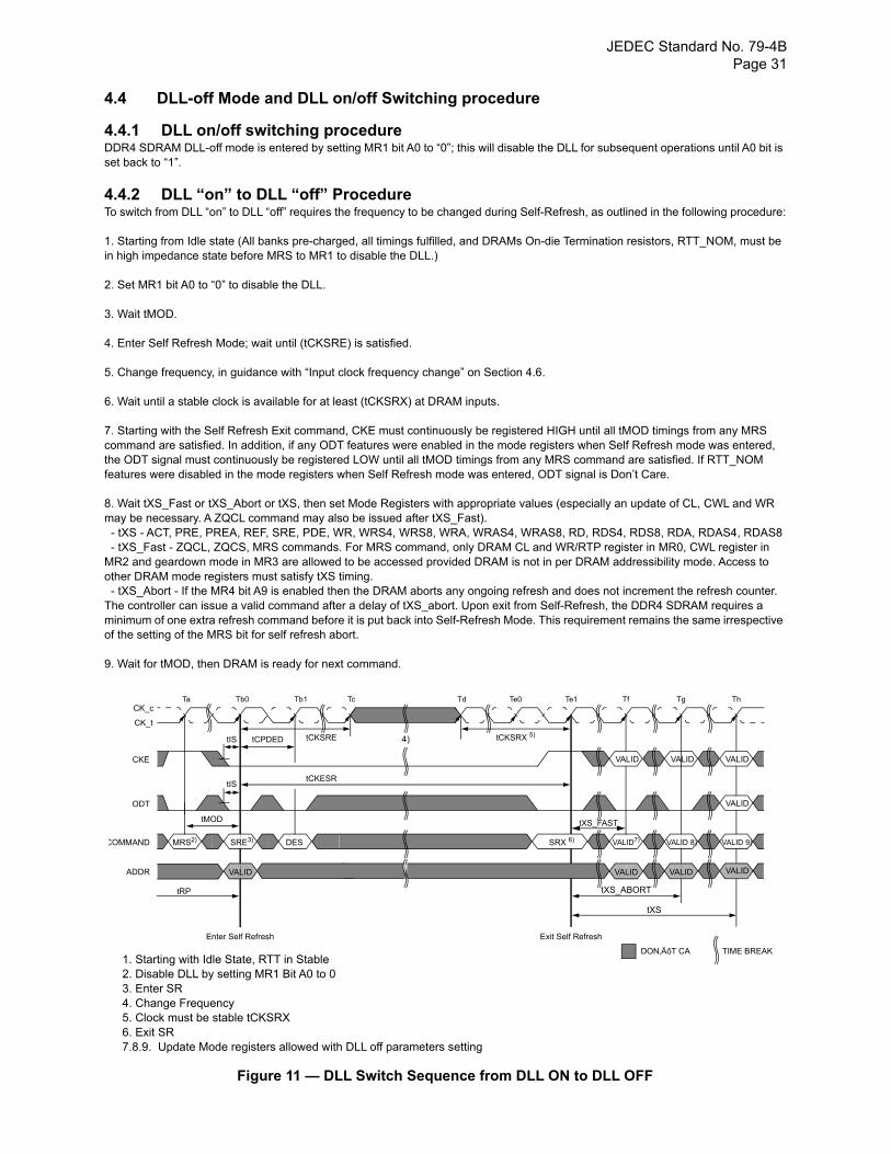
JEDEC Standard No. 79-4B Page 31
4.4 DLL-off Mode and DLL on/off Switching procedure
4.4.1 DLL on/off switching procedureDDR4 SDRAM DLL-off mode is entered by setting MR1 bit A0 to “0”; this will disable the DLL for subsequent operations until A0 bit is set back to “1”.
4.4.2 DLL “on” to DLL “off” ProcedureTo switch from DLL “on” to DLL “off” requires the frequency to be changed during Self-Refresh, as outlined in the following procedure:
1. Starting from Idle state (All banks pre-charged, all timings fulfilled, and DRAMs On-die Termination resistors, RTT_NOM, must be in high impedance state before MRS to MR1 to disable the DLL.)
2. Set MR1 bit A0 to “0” to disable the DLL.
3. Wait tMOD.
4. Enter Self Refresh Mode; wait until (tCKSRE) is satisfied.
5. Change frequency, in guidance with “Input clock frequency change” on Section 4.6.
6. Wait until a stable clock is available for at least (tCKSRX) at DRAM inputs.
7. Starting with the Self Refresh Exit command, CKE must continuously be registered HIGH until all tMOD timings from any MRS command are satisfied. In addition, if any ODT features were enabled in the mode registers when Self Refresh mode was entered, the ODT signal must continuously be registered LOW until all tMOD timings from any MRS command are satisfied. If RTT_NOM features were disabled in the mode registers when Self Refresh mode was entered, ODT signal is Don’t Care.
8. Wait tXS_Fast or tXS_Abort or tXS, then set Mode Registers with appropriate values (especially an update of CL, CWL and WR may be necessary. A ZQCL command may also be issued after tXS_Fast). - tXS - ACT, PRE, PREA, REF, SRE, PDE, WR, WRS4, WRS8, WRA, WRAS4, WRAS8, RD, RDS4, RDS8, RDA, RDAS4, RDAS8 - tXS_Fast - ZQCL, ZQCS, MRS commands. For MRS command, only DRAM CL and WR/RTP register in MR0, CWL register in MR2 and geardown mode in MR3 are allowed to be accessed provided DRAM is not in per DRAM addressibility mode. Access to other DRAM mode registers must satisfy tXS timing. - tXS_Abort - If the MR4 bit A9 is enabled then the DRAM aborts any ongoing refresh and does not increment the refresh counter. The controller can issue a valid command after a delay of tXS_abort. Upon exit from Self-Refresh, the DDR4 SDRAM requires a minimum of one extra refresh command before it is put back into Self-Refresh Mode. This requirement remains the same irrespective of the setting of the MRS bit for self refresh abort.
9. Wait for tMOD, then DRAM is ready for next command.
Figure 11 — DLL Switch Sequence from DLL ON to DLL OFF
Ta Tb0 Te1Te0Tb1 Tc Td Tf Tg Th
tIS tCPDED tCKSRE tCKSRX 5)
tCKESR
MRS2) SRE3) DES SRX 6) VALID7) VALID 9)
VALID
VALIDVALID
CK_c
CK_t
CKE
ODT
COMMAND
ADDR
tRP
Enter Self Refresh Exit Self Refresh
tXS_ABORT
tXS
tIS
DON’T CA TIME BREAK
VALIDVALID
VALID
tXS_FAST
VALID
4)
1. Starting with Idle State, RTT in Stable2. Disable DLL by setting MR1 Bit A0 to 03. Enter SR4. Change Frequency5. Clock must be stable tCKSRX6. Exit SR7.8.9. Update Mode registers allowed with DLL off parameters setting
VALID 8)
VALID
tMOD
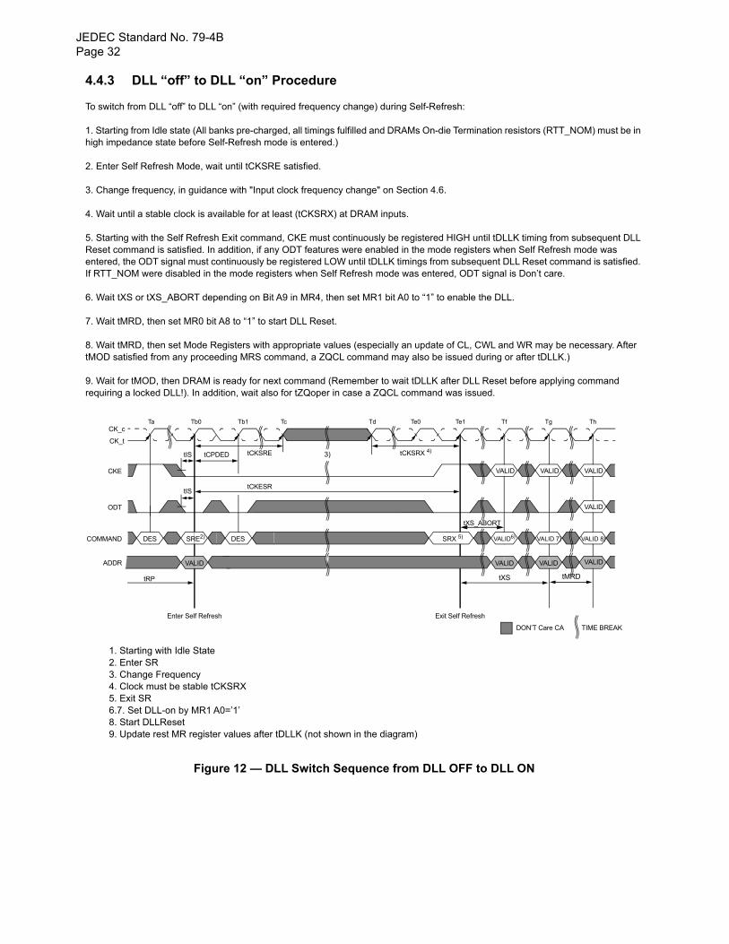
JEDEC Standard No. 79-4BPage 32
4.4.3 DLL “off” to DLL “on” Procedure
To switch from DLL “off” to DLL “on” (with required frequency change) during Self-Refresh:
1. Starting from Idle state (All banks pre-charged, all timings fulfilled and DRAMs On-die Termination resistors (RTT_NOM) must be in high impedance state before Self-Refresh mode is entered.)
2. Enter Self Refresh Mode, wait until tCKSRE satisfied.
3. Change frequency, in guidance with "Input clock frequency change" on Section 4.6.
4. Wait until a stable clock is available for at least (tCKSRX) at DRAM inputs.
5. Starting with the Self Refresh Exit command, CKE must continuously be registered HIGH until tDLLK timing from subsequent DLL Reset command is satisfied. In addition, if any ODT features were enabled in the mode registers when Self Refresh mode was entered, the ODT signal must continuously be registered LOW until tDLLK timings from subsequent DLL Reset command is satisfied. If RTT_NOM were disabled in the mode registers when Self Refresh mode was entered, ODT signal is Don’t care.
6. Wait tXS or tXS_ABORT depending on Bit A9 in MR4, then set MR1 bit A0 to “1” to enable the DLL.
7. Wait tMRD, then set MR0 bit A8 to “1” to start DLL Reset.
8. Wait tMRD, then set Mode Registers with appropriate values (especially an update of CL, CWL and WR may be necessary. After tMOD satisfied from any proceeding MRS command, a ZQCL command may also be issued during or after tDLLK.)
9. Wait for tMOD, then DRAM is ready for next command (Remember to wait tDLLK after DLL Reset before applying command requiring a locked DLL!). In addition, wait also for tZQoper in case a ZQCL command was issued.
Figure 12 — DLL Switch Sequence from DLL OFF to DLL ON
Ta Tb0 Te1Te0Tb1 Tc Td Tf Tg Th
tIS tCPDED tCKSRE tCKSRX 4)
tCKESR
DES SRE2) DES SRX 5) VALID6) VALID 8)
VALID
VALIDVALID
CK_c
CK_t
CKE
ODT
COMMAND
ADDR
tRP
Enter Self Refresh Exit Self Refresh
tXS
tIS
DON’T Care CA TIME BREAK
VALID
VALID
tXS_ABORT
VALID
3)
1. Starting with Idle State2. Enter SR3. Change Frequency4. Clock must be stable tCKSRX5. Exit SR6.7. Set DLL-on by MR1 A0=’1’8. Start DLLReset9. Update rest MR register values after tDLLK (not shown in the diagram)
VALID 7)
tMRD
VALIDVALID
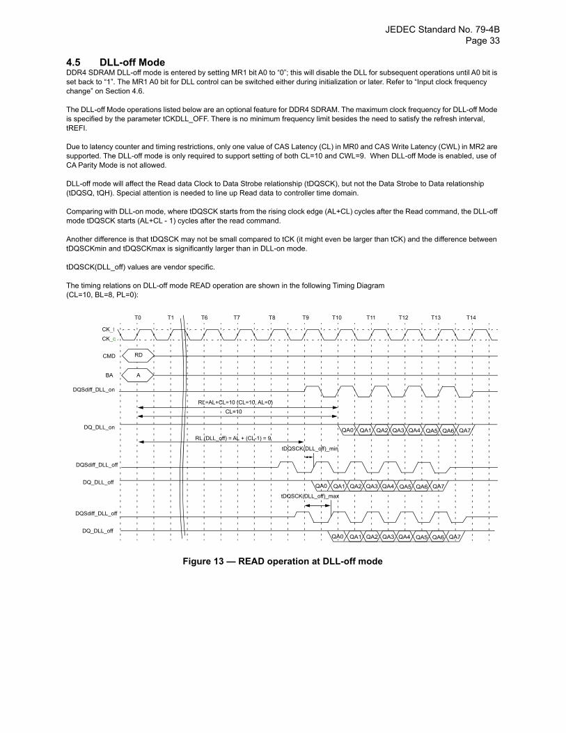
JEDEC Standard No. 79-4B Page 33
4.5 DLL-off ModeDDR4 SDRAM DLL-off mode is entered by setting MR1 bit A0 to “0”; this will disable the DLL for subsequent operations until A0 bit is set back to “1”. The MR1 A0 bit for DLL control can be switched either during initialization or later. Refer to “Input clock frequency change” on Section 4.6.
The DLL-off Mode operations listed below are an optional feature for DDR4 SDRAM. The maximum clock frequency for DLL-off Mode is specified by the parameter tCKDLL_OFF. There is no minimum frequency limit besides the need to satisfy the refresh interval, tREFI.
Due to latency counter and timing restrictions, only one value of CAS Latency (CL) in MR0 and CAS Write Latency (CWL) in MR2 are supported. The DLL-off mode is only required to support setting of both CL=10 and CWL=9. When DLL-off Mode is enabled, use of CA Parity Mode is not allowed.
DLL-off mode will affect the Read data Clock to Data Strobe relationship (tDQSCK), but not the Data Strobe to Data relationship (tDQSQ, tQH). Special attention is needed to line up Read data to controller time domain.
Comparing with DLL-on mode, where tDQSCK starts from the rising clock edge (AL+CL) cycles after the Read command, the DLL-off mode tDQSCK starts (AL+CL - 1) cycles after the read command.
Another difference is that tDQSCK may not be small compared to tCK (it might even be larger than tCK) and the difference between tDQSCKmin and tDQSCKmax is significantly larger than in DLL-on mode.
tDQSCK(DLL_off) values are vendor specific.
The timing relations on DLL-off mode READ operation are shown in the following Timing Diagram(CL=10, BL=8, PL=0):
Figure 13 — READ operation at DLL-off mode
CK_t
DQSdiff_DLL_on
T0 T1 T6 T7 T8 T9 T10 T11 T12 T13 T14
RD
ABA
CMD
DQ_DLL_on
RL=AL+CL=10 (CL=10, AL=0)
CL=10
RL (DLL_off) = AL + (CL-1) = 9
tDQSCK(DLL_off)_min
tDQSCK(DLL_off)_max
DQSdiff_DLL_off
DQ_DLL_off
DQSdiff_DLL_off
DQ_DLL_off
QA7QA6QA5QA4QA3QA2QA1QA0
QA7QA6QA5QA4QA3QA2QA1QA0
QA7QA6QA5QA4QA3QA2QA1QA0
CK_c
JEDEC Standard No. 79-4BPage 34
4.6 Input Clock Frequency Change
Once the DDR4 SDRAM is initialized, the DDR4 SDRAM requires the clock to be “stable” during almost all states of normal operation. This means that, once the clock frequency has been set and is to be in the “stable state”, the clock period is not allowed to deviate except for what is allowed for by the clock jitter and SSC (spread spectrum clocking) specifications.
The input clock frequency can be changed from one stable clock rate to another stable clock rate under Self- Refresh mode. Outside Self-Refresh mode, it is illegal to change the clock frequency.
Once the DDR4 SDRAM has been successfully placed into Self-Refresh mode and tCKSRE has been satisfied, the state of the clock becomes a don’t care. Once a don’t care, changing the clock frequency is permissible, provided the new clock frequency is stable prior to tCKSRX. When entering and exiting Self-Refresh mode for the sole purpose of changing the clock frequency, the Self-Refresh entry and exit specifications must still be met as outlined in Section 4.27 “Self-Refresh Operation”.
For the new clock frequency, additional MRS commands to MR0, MR2, MR3, MR4, MR5, and MR6 may need to be issued to program appropriate CL, CWL, Gear-down mode, Read & Write Preamble, Command Address Latency (CAL Mode), Command Address Parity (CA Parity Mode), and tCCD_L/tDLLK value.
In particular, the Command Address Parity Latency (PL) must be disabled when the clock rate changes, ie. while in Self Refresh Mode. For example, if changing the clock rate from DDR4-2133 to DDR4-2933 with CA Parity Mode enabled, MR5[2:0] must first change from PL = 4 to PL = disable prior to PL = 6. A correct procedure would be to (1) change PL = 4 to disable via MR5 [2:0], (2) enter Self Refresh Mode, (3) change clock rate from DDR4-2133 to DDR4-2933, (4) exit Self Refresh Mode, (5) Enable CA Parity Mode setting PL = 6 via MR5 [2:0].
If the MR settings that require additional clocks are updated after the clock rate has been increased, i.e. after exiting self refreshmode, the required MR settings must be updated prior to removing the DRAM from the IDLE state, unless the DRAM is RESET. If theDRAM leaves the idle state to enter self refresh mode or ZQ Calibration, the updating of the required MR settings may be deferred toafter the next time the DRAM enters the IDLE state.
If MR6 is issued prior to Self Refresh Entry for new tDLLK value, then DLL will relock automatically at Self Refresh Exit. However, if MR6 is issued after Self Refresh Entry, then MR0 must be issued to reset the DLL. The DDR4 SDRAM input clock frequency is allowed to change only within the minimum and maximum operating frequency specified for the particular speed grade. Any frequency change below the minimum operating frequency would require the use of DLL_on- mode -> DLL_off -mode transition sequence, refer to Section 4.4, DLL on/off switching procedure.
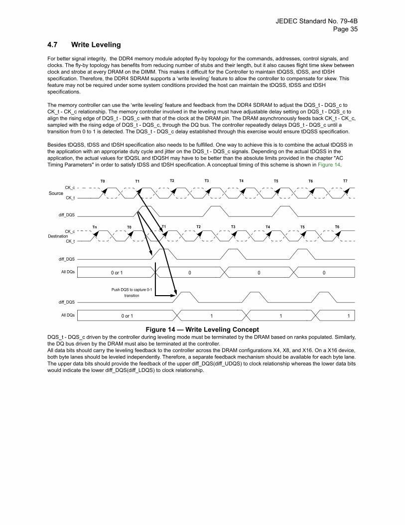
JEDEC Standard No. 79-4B Page 35
4.7 Write Leveling
For better signal integrity, the DDR4 memory module adopted fly-by topology for the commands, addresses, control signals, and clocks. The fly-by topology has benefits from reducing number of stubs and their length, but it also causes flight time skew between clock and strobe at every DRAM on the DIMM. This makes it difficult for the Controller to maintain tDQSS, tDSS, and tDSH specification. Therefore, the DDR4 SDRAM supports a ‘write leveling’ feature to allow the controller to compensate for skew. This feature may not be required under some system conditions provided the host can maintain the tDQSS, tDSS and tDSH specifications.
The memory controller can use the ‘write leveling’ feature and feedback from the DDR4 SDRAM to adjust the DQS_t - DQS_c to CK_t - CK_c relationship. The memory controller involved in the leveling must have adjustable delay setting on DQS_t - DQS_c to align the rising edge of DQS_t - DQS_c with that of the clock at the DRAM pin. The DRAM asynchronously feeds back CK_t - CK_c, sampled with the rising edge of DQS_t - DQS_c, through the DQ bus. The controller repeatedly delays DQS_t - DQS_c until a transition from 0 to 1 is detected. The DQS_t - DQS_c delay established through this exercise would ensure tDQSS specification.
Besides tDQSS, tDSS and tDSH specification also needs to be fulfilled. One way to achieve this is to combine the actual tDQSS in the application with an appropriate duty cycle and jitter on the DQS_t - DQS_c signals. Depending on the actual tDQSS in the application, the actual values for tDQSL and tDQSH may have to be better than the absolute limits provided in the chapter "AC Timing Parameters" in order to satisfy tDSS and tDSH specification. A conceptual timing of this scheme is shown in Figure 14.
Figure 14 — Write Leveling ConceptDQS_t - DQS_c driven by the controller during leveling mode must be terminated by the DRAM based on ranks populated. Similarly, the DQ bus driven by the DRAM must also be terminated at the controller.All data bits should carry the leveling feedback to the controller across the DRAM configurations X4, X8, and X16. On a X16 device, both byte lanes should be leveled independently. Therefore, a separate feedback mechanism should be available for each byte lane. The upper data bits should provide the feedback of the upper diff_DQS(diff_UDQS) to clock relationship whereas the lower data bits would indicate the lower diff_DQS(diff_LDQS) to clock relationship.
T0 T1 T2 T3 T4 T5 T6 T7
Tn T0 T1 T2 T3 T4 T5 T6
Source
Destination
CK_c
CK_t
diff_DQS
CK_c
CK_t
diff_DQS
diff_DQS
All DQs
All DQs
0 or 1 0 0 0
Push DQS to capture 0-1
transition
0 or 1 11 1
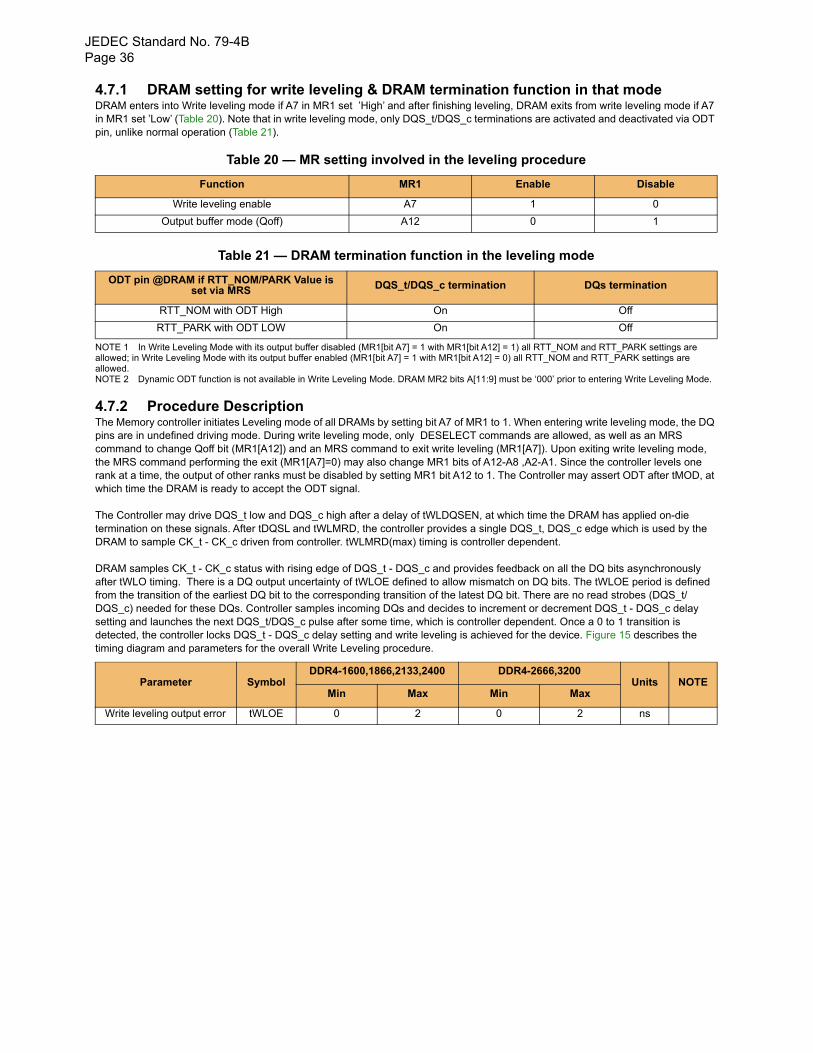
JEDEC Standard No. 79-4BPage 36
4.7.1 DRAM setting for write leveling & DRAM termination function in that modeDRAM enters into Write leveling mode if A7 in MR1 set ’High’ and after finishing leveling, DRAM exits from write leveling mode if A7 in MR1 set ’Low’ (Table 20). Note that in write leveling mode, only DQS_t/DQS_c terminations are activated and deactivated via ODT pin, unlike normal operation (Table 21).
Table 20 — MR setting involved in the leveling procedure
Table 21 — DRAM termination function in the leveling mode
NOTE 1 In Write Leveling Mode with its output buffer disabled (MR1[bit A7] = 1 with MR1[bit A12] = 1) all RTT_NOM and RTT_PARK settings are allowed; in Write Leveling Mode with its output buffer enabled (MR1[bit A7] = 1 with MR1[bit A12] = 0) all RTT_NOM and RTT_PARK settings are allowed. NOTE 2 Dynamic ODT function is not available in Write Leveling Mode. DRAM MR2 bits A[11:9] must be ‘000’ prior to entering Write Leveling Mode.
4.7.2 Procedure DescriptionThe Memory controller initiates Leveling mode of all DRAMs by setting bit A7 of MR1 to 1. When entering write leveling mode, the DQ pins are in undefined driving mode. During write leveling mode, only DESELECT commands are allowed, as well as an MRS command to change Qoff bit (MR1[A12]) and an MRS command to exit write leveling (MR1[A7]). Upon exiting write leveling mode, the MRS command performing the exit (MR1[A7]=0) may also change MR1 bits of A12-A8 ,A2-A1. Since the controller levels one rank at a time, the output of other ranks must be disabled by setting MR1 bit A12 to 1. The Controller may assert ODT after tMOD, at which time the DRAM is ready to accept the ODT signal.
The Controller may drive DQS_t low and DQS_c high after a delay of tWLDQSEN, at which time the DRAM has applied on-die termination on these signals. After tDQSL and tWLMRD, the controller provides a single DQS_t, DQS_c edge which is used by the DRAM to sample CK_t - CK_c driven from controller. tWLMRD(max) timing is controller dependent.
DRAM samples CK_t - CK_c status with rising edge of DQS_t - DQS_c and provides feedback on all the DQ bits asynchronously after tWLO timing. There is a DQ output uncertainty of tWLOE defined to allow mismatch on DQ bits. The tWLOE period is defined from the transition of the earliest DQ bit to the corresponding transition of the latest DQ bit. There are no read strobes (DQS_t/DQS_c) needed for these DQs. Controller samples incoming DQs and decides to increment or decrement DQS_t - DQS_c delay setting and launches the next DQS_t/DQS_c pulse after some time, which is controller dependent. Once a 0 to 1 transition is detected, the controller locks DQS_t - DQS_c delay setting and write leveling is achieved for the device. Figure 15 describes the timing diagram and parameters for the overall Write Leveling procedure.
Function MR1 Enable Disable
Write leveling enable A7 1 0
Output buffer mode (Qoff) A12 0 1
ODT pin @DRAM if RTT_NOM/PARK Value is set via MRS DQS_t/DQS_c termination DQs termination
RTT_NOM with ODT High On Off
RTT_PARK with ODT LOW On Off
Parameter Symbol DDR4-1600,1866,2133,2400 DDR4-2666,3200
Units NOTE Min Max Min Max
Write leveling output error tWLOE 0 2 0 2 ns
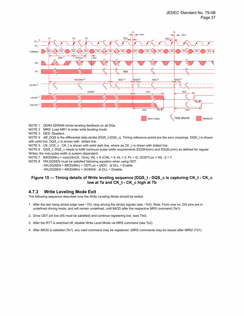
JEDEC Standard No. 79-4B Page 37
NOTE 1 DDR4 SDRAM drives leveling feedback on all DQs. NOTE 2 MRS: Load MR1 to enter write leveling mode.NOTE 3 DES: Deselect.NOTE 4 diff_DQS is the differential data strobe (DQS_t-DQS_c). Timing reference points are the zero crossings. DQS_t is shown with solid line, DQS_c is shown with dotted line.NOTE 5 CK_t/CK_c : CK_t is shown with solid dark line, where as CK_c is drawn with dotted line.NOTE 6 DQS_t, DQS_c needs to fulfill minimum pulse width requirements tDQSH(min) and tDQSL(min) as defined for regular Writes; the max pulse width is system dependent.NOTE 7 tMOD(Min) = max(24nCK, 15ns), WL = 9 (CWL = 9, AL = 0, PL = 0), DODTLon = WL -2 = 7.NOTE 8 tWLDQSEN must be satisfied following equation when using ODT. - tWLDQSEN > tMOD(Min) + ODTLon + tADC: at DLL = Enable - tWLDQSEN > tMOD(Min) + tAONAS: at DLL = Disable
Figure 15 — Timing details of Write leveling sequence [DQS_t - DQS_c is capturing CK_t - CK_c low at Ta and CK_t - CK_c high at Tb
4.7.3 Write Leveling Mode ExitThe following sequence describes how the Write Leveling Mode should be exited:
1. After the last rising strobe edge (see ~T0), stop driving the strobe signals (see ~Tc0). Note: From now on, DQ pins are in undefined driving mode, and will remain undefined, until tMOD after the respective MRS command (Te1).
2. Drive ODT pin low (tIS must be satisfied) and continue registering low. (see Tb0).
3. After the RTT is switched off, disable Write Level Mode via MRS command (see Tc2).
4. After tMOD is satisfied (Te1), any valid command may be registered. (MRS commands may be issued after tMRD (Td1).
T24 T31
Ta
tADCtMOD (7)
T0
CK_c
CK_t
COMMAND
ODT
Late DQs (1)
Early DQs (1)
MRS DES DES DES DES DES DES DES DES DES DES DES DES
Tb
tWLS
tWLH
tWLS
tWLH
RTT
DES
tWLDQSEN (8) tDQSL (6) tDQSH (6) tDQSL (6) tDQSH (6)
diff_DQS (4)
tWLMRD tWLO
tWLO tWLOE
tWLOE
tWLO
tWLO
DODTLon (7)
(2) (3)
(5)
Valid
Don’t Care INVALIDTIME BRAKE
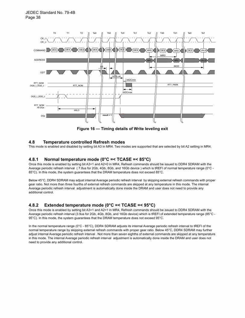
JEDEC Standard No. 79-4BPage 38
Figure 16 — Timing details of Write leveling exit
4.8 Temperature controlled Refresh modes This mode is enabled and disabled by setting bit A3 in MR4. Two modes are supported that are selected by bit A2 setting in MR4.
4.8.1 Normal temperature mode (0°C =< TCASE =< 85°C)Once this mode is enabled by setting bit A3=1 and A2=0 in MR4, Refresh commands should be issued to DDR4 SDRAM with the Average periodic refresh interval ( 7.8us for 2Gb, 4Gb, 8Gb, and 16Gb device ) which is tREFI of normal temperature range (0°C - 85°C). In this mode, the system guarantees that the DRAM temperature does not exceed 85°C.
Below 45°C, DDR4 SDRAM may adjust internal Average periodic refresh interval by skipping external refresh commands with proper gear ratio. Not more than three fourths of external refresh commands are skipped at any temperature in this mode. The internal Average periodic refresh interval adjustment is automatically done inside the DRAM and user does not need to provide any additional control.
4.8.2 Extended temperature mode (0°C =< TCASE =< 95°C)Once this mode is enabled by setting bit A3=1 and A2=1 in MR4, Refresh commands should be issued to DDR4 SDRAM with the Average periodic refresh interval (3.9us for 2Gb, 4Gb, 8Gb, and 16Gb device) which is tREFI of extended temperature range (85°C - 95°C). In this mode, the system guarantees that the DRAM temperature does not exceed 95°C.
In the normal temperature range (0°C - 85°C), DDR4 SDRAM adjusts its internal Average periodic refresh interval to tREFI of the normal temperature range by skipping external refresh commands with proper gear ratio. Below 45°C, DDR4 SDRAM may further adjust internal Average periodic refresh interval . Not more than seven eighths of external commands are skipped at any temperature in this mode. The internal Average periodic refresh interval adjustment is automatically done inside the DRAM and user does not need to provide any additional control.
CK_t
CK_c
T0 T1 T2 Ta0 Tb0 Tc0 Tc1 Tc2 Td0 Td1 Te0 Te1
COMMAND DES DESDES DES DESDESDESDES DES
MRxADDRESS
ODT
tADCmin
tADCmax
MRS
MR1
MRS
tWLO
result = 1
RTT_NOM
tMRD
tMOD
VALID
VALID
ODTLoff
tIS
RTT_NOM
DQS_t_DQS_c
RTT_NOM
DQs
DQS_t_DQS_c
All DQs
RTT_PARK
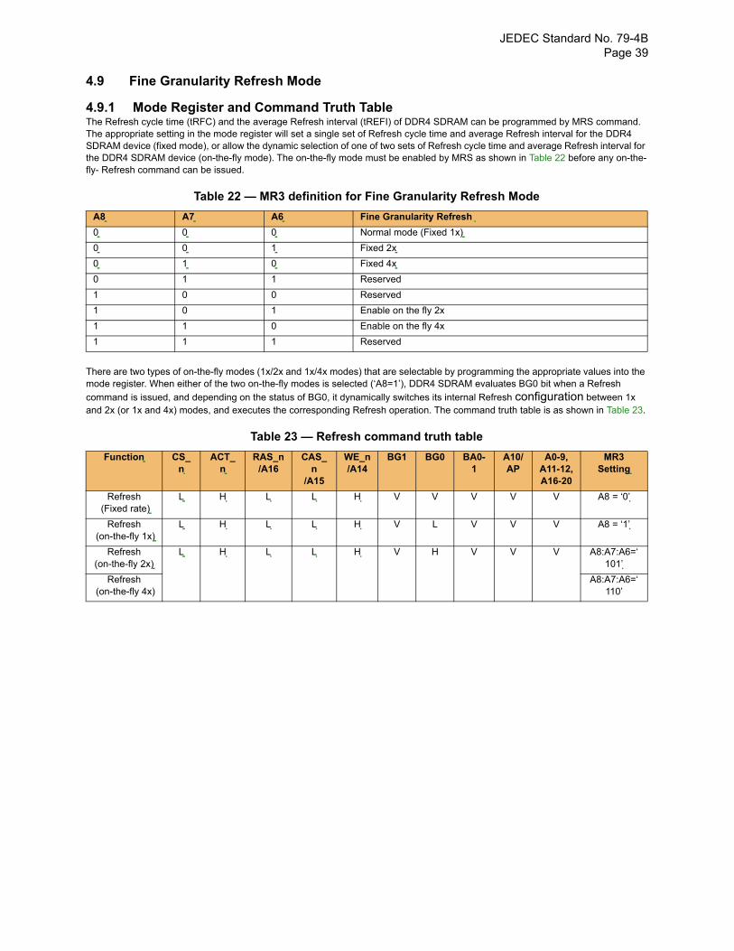
JEDEC Standard No. 79-4B Page 39
4.9 Fine Granularity Refresh Mode
4.9.1 Mode Register and Command Truth TableThe Refresh cycle time (tRFC) and the average Refresh interval (tREFI) of DDR4 SDRAM can be programmed by MRS command. The appropriate setting in the mode register will set a single set of Refresh cycle time and average Refresh interval for the DDR4 SDRAM device (fixed mode), or allow the dynamic selection of one of two sets of Refresh cycle time and average Refresh interval for the DDR4 SDRAM device (on-the-fly mode). The on-the-fly mode must be enabled by MRS as shown in Table 22 before any on-the-fly- Refresh command can be issued.
Table 22 — MR3 definition for Fine Granularity Refresh Mode
There are two types of on-the-fly modes (1x/2x and 1x/4x modes) that are selectable by programming the appropriate values into the mode register. When either of the two on-the-fly modes is selected (‘A8=1’), DDR4 SDRAM evaluates BG0 bit when a Refresh
command is issued, and depending on the status of BG0, it dynamically switches its internal Refresh configuration between 1x and 2x (or 1x and 4x) modes, and executes the corresponding Refresh operation. The command truth table is as shown in Table 23.
Table 23 — Refresh command truth table
A8 A7 A6 Fine Granularity Refresh
0 0 0 Normal mode (Fixed 1x)
0 0 1 Fixed 2x
0 1 0 Fixed 4x
0 1 1 Reserved
1 0 0 Reserved
1 0 1 Enable on the fly 2x
1 1 0 Enable on the fly 4x
1 1 1 Reserved
Function CS_n
ACT_n
RAS_n/A16
CAS_n
/A15
WE_n/A14
BG1 BG0 BA0-1
A10/AP
A0-9, A11-12, A16-20
MR3 Setting
Refresh (Fixed rate)
L H L L H V V V V V A8 = ‘0’
Refresh (on-the-fly 1x)
L H L L H V L V V V A8 = ‘1’
Refresh (on-the-fly 2x)
L H L L H V H V V V A8:A7:A6=‘101’
Refresh (on-the-fly 4x)
A8:A7:A6=‘110’
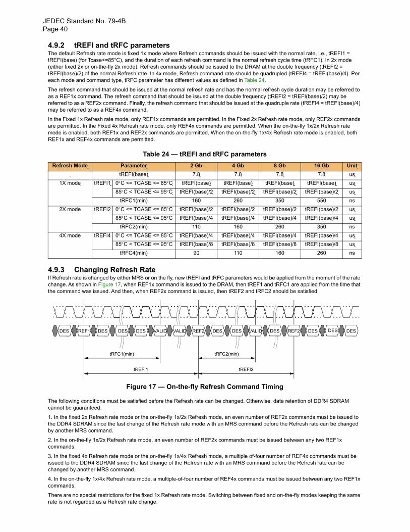
JEDEC Standard No. 79-4BPage 40
4.9.2 tREFI and tRFC parametersThe default Refresh rate mode is fixed 1x mode where Refresh commands should be issued with the normal rate, i.e., tREFI1 = tREFI(base) (for Tcase<=85°C), and the duration of each refresh command is the normal refresh cycle time (tRFC1). In 2x mode (either fixed 2x or on-the-fly 2x mode), Refresh commands should be issued to the DRAM at the double frequency (tREFI2 = tREFI(base)/2) of the normal Refresh rate. In 4x mode, Refresh command rate should be quadrupled (tREFI4 = tREFI(base)/4). Per each mode and command type, tRFC parameter has different values as defined in Table 24.
The refresh command that should be issued at the normal refresh rate and has the normal refresh cycle duration may be referred to as a REF1x command. The refresh command that should be issued at the double frequency (tREFI2 = tREFI(base)/2) may be referred to as a REF2x command. Finally, the refresh command that should be issued at the quadruple rate (tREFI4 = tREFI(base)/4) may be referred to as a REF4x command.
In the Fixed 1x Refresh rate mode, only REF1x commands are permitted. In the Fixed 2x Refresh rate mode, only REF2x commands are permitted. In the Fixed 4x Refresh rate mode, only REF4x commands are permitted. When the on-the-fly 1x/2x Refresh rate mode is enabled, both REF1x and REF2x commands are permitted. When the on-the-fly 1x/4x Refresh rate mode is enabled, both REF1x and REF4x commands are permitted.
Table 24 — tREFI and tRFC parameters
4.9.3 Changing Refresh RateIf Refresh rate is changed by either MRS or on the fly, new tREFI and tRFC parameters would be applied from the moment of the rate change. As shown in Figure 17, when REF1x command is issued to the DRAM, then tREF1 and tRFC1 are applied from the time that the command was issued. And then, when REF2x command is issued, then tREF2 and tRFC2 should be satisfied.
Figure 17 — On-the-fly Refresh Command Timing
The following conditions must be satisfied before the Refresh rate can be changed. Otherwise, data retention of DDR4 SDRAM cannot be guaranteed.
1. In the fixed 2x Refresh rate mode or the on-the-fly 1x/2x Refresh mode, an even number of REF2x commands must be issued to the DDR4 SDRAM since the last change of the Refresh rate mode with an MRS command before the Refresh rate can be changed by another MRS command.
2. In the on-the-fly 1x/2x Refresh rate mode, an even number of REF2x commands must be issued between any two REF1x commands.
3. In the fixed 4x Refresh rate mode or the on-the-fly 1x/4x Refresh mode, a multiple of-four number of REF4x commands must be issued to the DDR4 SDRAM since the last change of the Refresh rate with an MRS command before the Refresh rate can be changed by another MRS command.
4. In the on-the-fly 1x/4x Refresh rate mode, a multiple-of-four number of REF4x commands must be issued between any two REF1x commands.
There are no special restrictions for the fixed 1x Refresh rate mode. Switching between fixed and on-the-fly modes keeping the same rate is not regarded as a Refresh rate change.
Refresh Mode Parameter 2 Gb 4 Gb 8 Gb 16 Gb Unit
tREFI(base) 7.8 7.8 7.8 7.8 us
1X mode tREFI1 0C <= TCASE <= 85C tREFI(base) tREFI(base) tREFI(base) tREFI(base) us
85C < TCASE <= 95C tREFI(base)/2 tREFI(base)/2 tREFI(base)/2 tREFI(base)/2 us
tRFC1(min) 160 260 350 550 ns
2X mode tREFI2 0C <= TCASE <= 85C tREFI(base)/2 tREFI(base)/2 tREFI(base)/2 tREFI(base)/2 us
85C < TCASE <= 95C tREFI(base)/4 tREFI(base)/4 tREFI(base)/4 tREFI(base)/4 us
tRFC2(min) 110 160 260 350 ns
4X mode tREFI4 0C <= TCASE <= 85C tREFI(base)/4 tREFI(base)/4 tREFI(base)/4 tREFI(base)/4 us
85C < TCASE <= 95C tREFI(base)/8 tREFI(base)/8 tREFI(base)/8 tREFI(base)/8 us
tRFC4(min) 90 110 160 260 ns
DESREF1 DESDES DES DESDES
tRFC1(min)
REF2 VALIDVALID DES DESVALID DES REF2DES
tRFC2(min)
tREFI1 tREFI2
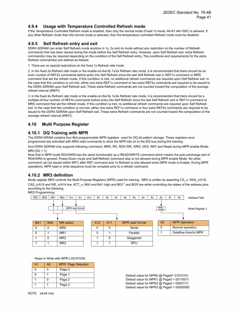
JEDEC Standard No. 79-4B Page 41
4.9.4 Usage with Temperature Controlled Refresh modeIf the Temperature Controlled Refresh mode is enabled, then only the normal mode (Fixed 1x mode; A8:A7:A6=’000’) is allowed. If any other Refresh mode than the normal mode is selected, then the temperature controlled Refresh mode must be disabled.
4.9.5 Self Refresh entry and exitDDR4 SDRAM can enter Self Refresh mode anytime in 1x, 2x and 4x mode without any restriction on the number of Refresh commands that has been issued during the mode before the Self Refresh entry. However, upon Self Refresh exit, extra Refresh command(s) may be required depending on the condition of the Self Refresh entry. The conditions and requirements for the extra Refresh command(s) are defined as follows;
1. There are no special restrictions on the fixed 1x Refresh rate mode.
2. In the fixed 2x Refresh rate mode or the enable-on-the-fly 1x/2x Refresh rate mode, it is recommended that there should be an even number of REF2x commands before entry into Self Refresh since the last Self Refresh exit or REF1x command or MRS command that set the refresh mode. If this condition is met, no additional refresh commands are required upon Self Refresh exit. In the case that this condition is not met, either one extra REF1x command or two extra REF2x commands are required to be issued to the DDR4 SDRAM upon Self Refresh exit. These extra Refresh commands are not counted toward the computation of the average refresh interval (tREFI).
3. In the fixed 4x Refresh rate mode or the enable-on-the-fly 1x/4x Refresh rate mode, it is recommended that there should be a multiple-of-four number of REF4x commands before entry into Self Refresh since the last Self Refresh exit or REF1x command or MRS command that set the refresh mode. If this condition is met, no additional refresh commands are required upon Self Refresh exit. In the case that this condition is not met, either one extra REF1x command or four extra REF4x commands are required to be issued to the DDR4 SDRAM upon Self Refresh exit. These extra Refresh commands are not counted toward the computation of the average refresh interval (tREFI).
4.10 Multi Purpose Register
4.10.1 DQ Training with MPRThe DDR4 DRAM contains four 8bit programmable MPR registers used for DQ bit pattern storage. These registers once programmed are activated with MRS read commands to drive the MPR bits on to the DQ bus during link training.
And DDR4 SDRAM only supports following command, MRS, RD, RDA WR, WRA, DES, REF and Reset during MPR enable Mode: MR3 [A2 = 1].Note that in MPR mode RDA/WRA has the same functionality as a READ/WRITE command which means the auto precharge part of RDA/WRA is ignored. Power-Down mode and Self-Refresh command also is not allowed during MPR enable Mode. No other command can be issued within tRFC after REF command and 1x Refresh is only allowed when MPR mode is Enable. During MPR operations, MPR read or write sequence must be complete prior to a refresh command.
4.10.2 MR3 definitionMode register MR3 controls the Multi-Purpose Registers (MPR) used for training. MR3 is written by asserting CS_n, RAS_n/A16,
CAS_n/A15 and WE_n/A14 low, ACT_n, BA0 and BA1 high and BG11 and BG0 low while controlling the states of the address pins according to the following:MR3 Programming:
NOTE x4/x8 only
Address Field
A12 A11 MPR read format
0 0 Serial
0 1 Parallel
1 0 Staggered
1 1 RFU
BA1 BA0 MR select
0 0 MR0
0 1 MR1
1 0 MR2
1 1 MR3
Mode Register 3
BG0 BA1 A11 A10 A9 A8 A7 A6 A5 A4 A3 A2 A1 A0
MPR read format 1 MPR
Read or Write with MPR LOCATION:
A1 A0 MPR Page Selection
0 0 Page 0
0 1 Page 1
1 0 Page 2
1 1 Page 3
BA0
1
A2 MPR Operation
0 Normal operation
1 Dataflow from/to MPR
BG1 A12
enable
Default value for MPR0 @ Page0= 01010101Default value for MPR1 @ Page0 = 00110011Default value for MPR2 @ Page0 = 00001111Default value for MPR3 @ Page0 = 00000000
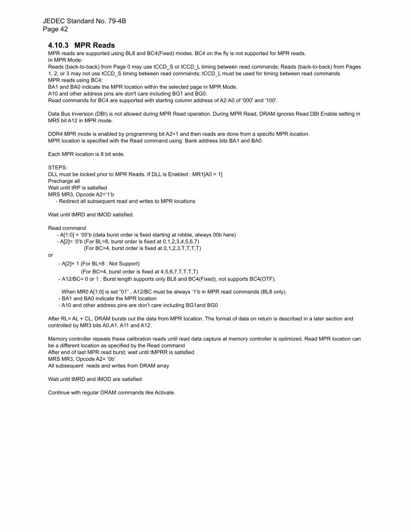
JEDEC Standard No. 79-4BPage 42
4.10.3 MPR Reads MPR reads are supported using BL8 and BC4(Fixed) modes. BC4 on the fly is not supported for MPR reads.In MPR Mode:Reads (back-to-back) from Page 0 may use tCCD_S or tCCD_L timing between read commands; Reads (back-to-back) from Pages 1, 2, or 3 may not use tCCD_S timing between read commands; tCCD_L must be used for timing between read commandsMPR reads using BC4:BA1 and BA0 indicate the MPR location within the selected page in MPR Mode.A10 and other address pins are don't care including BG1 and BG0.Read commands for BC4 are supported with starting column address of A2:A0 of '000' and '100'.
Data Bus Inversion (DBI) is not allowed during MPR Read operation. During MPR Read, DRAM ignores Read DBI Enable setting in MR5 bit A12 in MPR mode.
DDR4 MPR mode is enabled by programming bit A2=1 and then reads are done from a specific MPR location. MPR location is specified with the Read command using Bank address bits BA1 and BA0.
Each MPR location is 8 bit wide.
STEPS:DLL must be locked prior to MPR Reads. If DLL is Enabled : MR1[A0 = 1]Precharge allWait until tRP is satisfiedMRS MR3, Opcode A2=’1’b - Redirect all subsequent read and writes to MPR locations
Wait until tMRD and tMOD satisfied.
Read command - A[1:0] = ‘00’b (data burst order is fixed starting at nibble, always 00b here) - A[2]= ‘0’b (For BL=8, burst order is fixed at 0,1,2,3,4,5,6,7) (For BC=4, burst order is fixed at 0,1,2,3,T,T,T,T) or
- A[2]= 1 (For BL=8 : Not Support)
(For BC=4, burst order is fixed at 4,5,6,7,T,T,T,T) - A12/BC= 0 or 1 : Burst length supports only BL8 and BC4(Fixed), not supports BC4(OTF). When MR0 A[1:0] is set “01” , A12/BC must be always ‘1’b in MPR read commands (BL8 only). - BA1 and BA0 indicate the MPR location - A10 and other address pins are don’t care including BG1and BG0
After RL= AL + CL, DRAM bursts out the data from MPR location. The format of data on return is described in a later section and controlled by MR3 bits A0,A1, A11 and A12.
Memory controller repeats these calibration reads until read data capture at memory controller is optimized. Read MPR location can be a different location as specified by the Read commandAfter end of last MPR read burst, wait until tMPRR is satisfiedMRS MR3, Opcode A2= ‘0b’All subsequent reads and writes from DRAM array
Wait until tMRD and tMOD are satisfied
Continue with regular DRAM commands like Activate.
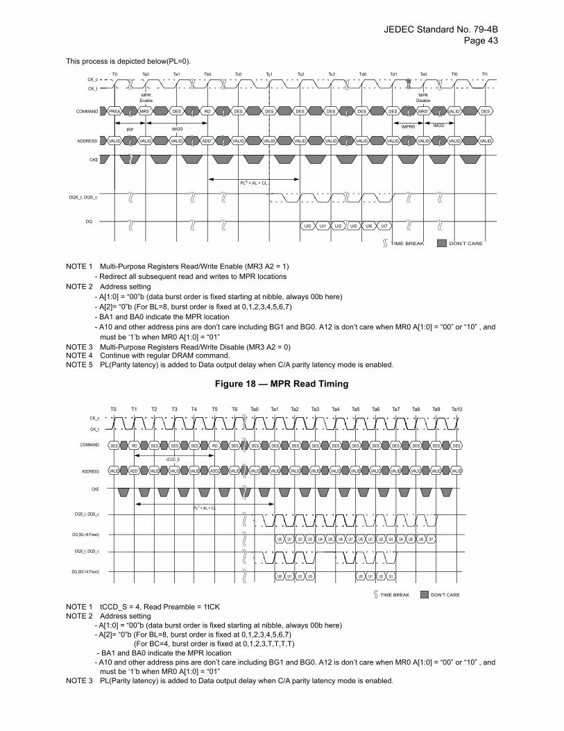
JEDEC Standard No. 79-4B Page 43
This process is depicted below(PL=0).
NOTE 1 Multi-Purpose Registers Read/Write Enable (MR3 A2 = 1) - Redirect all subsequent read and writes to MPR locations
NOTE 2 Address setting - A[1:0] = “00”b (data burst order is fixed starting at nibble, always 00b here) - A[2]= “0”b (For BL=8, burst order is fixed at 0,1,2,3,4,5,6,7) - BA1 and BA0 indicate the MPR location - A10 and other address pins are don’t care including BG1 and BG0. A12 is don’t care when MR0 A[1:0] = “00” or “10” , and
must be ‘1’b when MR0 A[1:0] = “01”NOTE 3 Multi-Purpose Registers Read/Write Disable (MR3 A2 = 0)NOTE 4 Continue with regular DRAM command.NOTE 5 PL(Parity latency) is added to Data output delay when C/A parity latency mode is enabled.
Figure 18 — MPR Read Timing
NOTE 1 tCCD_S = 4, Read Preamble = 1tCKNOTE 2 Address setting
- A[1:0] = “00”b (data burst order is fixed starting at nibble, always 00b here) - A[2]= “0”b (For BL=8, burst order is fixed at 0,1,2,3,4,5,6,7) (For BC=4, burst order is fixed at 0,1,2,3,T,T,T,T) - BA1 and BA0 indicate the MPR location - A10 and other address pins are don’t care including BG1 and BG0. A12 is don’t care when MR0 A[1:0] = “00” or “10” , and
must be ‘1’b when MR0 A[1:0] = “01”NOTE 3 PL(Parity latency) is added to Data output delay when C/A parity latency mode is enabled.
DES
Ta0 Ta1 Tc2 Tc3 Td0 Td1Tb0 Tf1
RD DES DES
T0
MRS1
CK_c
CK_t
COMMAND
ADDRESS
DQS_t, DQS_c
CKE
TIME BREAK DON’T CARE
Tc0 Tc1
DESPREA DES DES DES DES MRS3 VALID4
Te0 Tf0
VALID ADD2 VALID VALIDVALID VALIDVALID VALID VALID VALID VALID VALID VALID
tRPtMOD
tMOD
MPREnable
MPRDisable
PL5 + AL + CL
DQUI7UI1 UI5UI0 UI2 UI6
tMPRR
CK_c
CK_t
T0 T1 T2 T3 T4 T5 T6 Ta0 Ta1 Ta2 Ta3 Ta4 Ta5 Ta6 Ta7 Ta8 Ta9 Ta10
COMMAND DES RD DES DES DES RD DES DES DES DES DES DES DES DES DES DES DES DES
VALID ADD2 VALID VALID VALID ADD2 VALID VALID VALID VALID VALID VALID VALID VALID VALID VALID VALID VALID
UI1UI0 UI3UI2 UI5UI4 UI7UI6 UI1UI0 UI3UI2 UI5UI4 UI7UI6
TIME BREAK DON’T CARE
tCCD_S
PL3 + AL + CL
ADDRESS
CKE
DQS_t, DQS_c
DQ (BL=8:Fixed)
UI1UI0 UI3UI2 UI1UI0 UI3UI2
DQS_t, DQS_c
DQ (BC=4:Fixed)
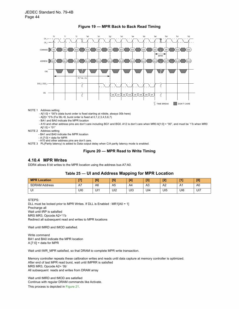
JEDEC Standard No. 79-4BPage 44
Figure 19 — MPR Back to Back Read Timing
NOTE 1 Address setting - A[1:0] = “00”b (data burst order is fixed starting at nibble, always 00b here) - A[2]= “0”b (For BL=8, burst order is fixed at 0,1,2,3,4,5,6,7) - BA1 and BA0 indicate the MPR location - A10 and other address pins are don’t care including BG1 and BG0. A12 is don’t care when MR0 A[1:0] = “00”, and must be ‘1’b when MR0 A[1:0] = “01”
NOTE 2 Address setting - BA1 and BA0 indicate the MPR location - A [7:0] = data for MPR
- A10 and other address pins are don’t care.NOTE 3 PL(Parity latency) is added to Data output delay when C/A parity latency mode is enabled.
Figure 20 — MPR Read to Write Timing
4.10.4 MPR WritesDDR4 allows 8 bit writes to the MPR location using the address bus A7:A0.
Table 25 — UI and Address Mapping for MPR Location
STEPS:DLL must be locked prior to MPR Writes. If DLL is Enabled : MR1[A0 = 1]Precharge allWait until tRP is satisfiedMRS MR3, Opcode A2=’1’bRedirect all subsequent read and writes to MPR locations
Wait until tMRD and tMOD satisfied.
Write commandBA1 and BA0 indicate the MPR location A [7:0] = data for MPR
Wait until tWR_MPR satisfied, so that DRAM to complete MPR write transaction. Memory controller repeats these calibration writes and reads until data capture at memory controller is optimized. After end of last MPR read burst, wait until tMPRR is satisfiedMRS MR3, Opcode A2= ‘0b’All subsequent reads and writes from DRAM array
Wait until tMRD and tMOD are satisfiedContinue with regular DRAM commands like Activate.
This process is depicted in Figure 21.
MPR Location [7] [6] [5] [4] [3] [2] [1] [0]
SDRAM Address A7 A6 A5 A4 A3 A2 A1 A0
UI UI0 UI1 UI2 UI3 UI4 UI5 UI6 UI7
DES
T1 T2 Ta3 Ta4 Ta5 Ta6Ta0 Tb2
DES DES DES
T0
DES
CK_c
CK_t
COMMAND
ADDRESS
DQS_t, DQS_c
CKE
TIME BREAK DON’T CARE
Ta1 Ta2
DESRD DES DES DES DES WR DES
Tb0 Tb1
VALID VALID VALID VALIDVALID VALIDADD1 VALID VALID VALID VALID ADD2 VALID
PL3 +AL + CL
DQUI7UI3 UI5UI2 UI4 UI6UI1UI0
tMPRR
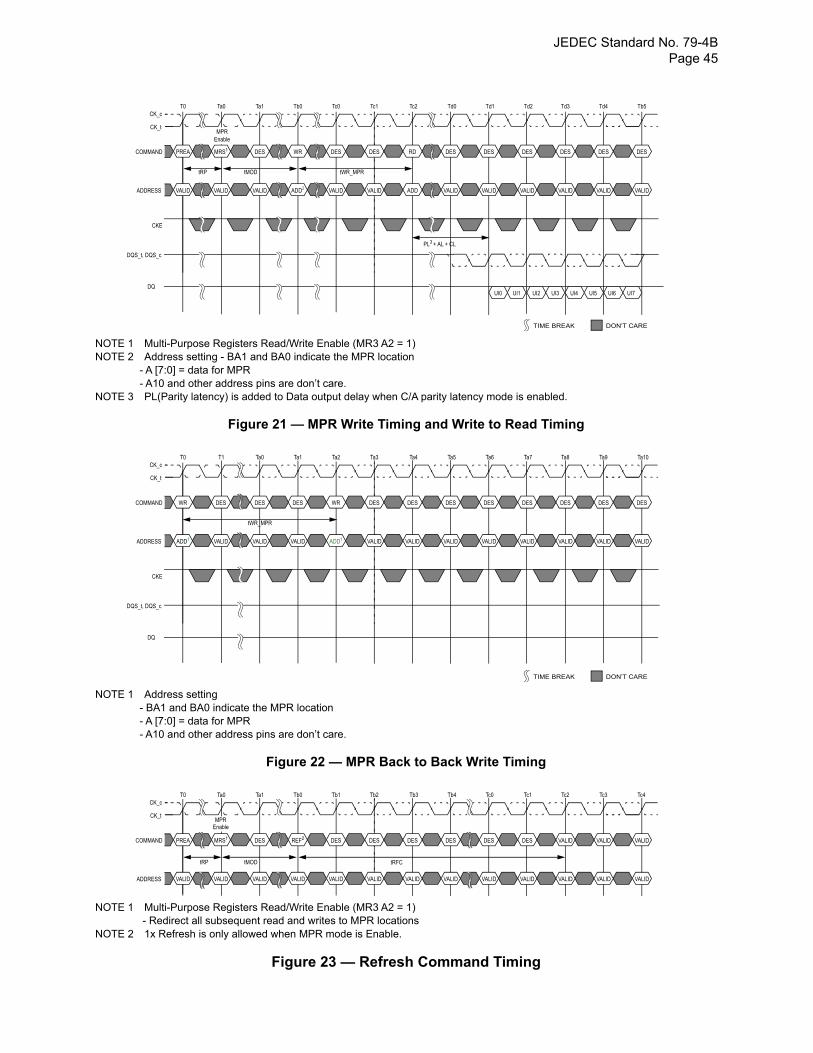
JEDEC Standard No. 79-4B Page 45
NOTE 1 Multi-Purpose Registers Read/Write Enable (MR3 A2 = 1) NOTE 2 Address setting - BA1 and BA0 indicate the MPR location - A [7:0] = data for MPR - A10 and other address pins are don’t care. NOTE 3 PL(Parity latency) is added to Data output delay when C/A parity latency mode is enabled.
Figure 21 — MPR Write Timing and Write to Read Timing
NOTE 1 Address setting - BA1 and BA0 indicate the MPR location - A [7:0] = data for MPR - A10 and other address pins are don’t care.
Figure 22 — MPR Back to Back Write Timing
NOTE 1 Multi-Purpose Registers Read/Write Enable (MR3 A2 = 1) - Redirect all subsequent read and writes to MPR locationsNOTE 2 1x Refresh is only allowed when MPR mode is Enable.
Figure 23 — Refresh Command Timing
DES
Ta0 Ta1 Tc2 Td0 Td1 Td2Tb0 Tb5
WR DES DES
T0
MRS1
CK_c
CK_t
COMMAND
ADDRESS
DQS_t, DQS_c
CKE
TIME BREAK DON’T CARE
Tc0 Tc1
DESPREA DES RD DES DES DES DES
Td3 Td4
VALID ADD2 VALID VALIDVALID VALIDVALID VALID ADD VALID VALID VALID VALID
PL3 + AL + CL
DQUI7UI3 UI5UI2 UI4 UI6UI1UI0
MPREnable
tRP tMOD tWR_MPR
DES
T1 Ta0 Ta4 Ta5 Ta6 Ta7Ta1 Ta10
DES DES DES
T0
DES
CK_c
CK_t
COMMAND
ADDRESS
DQS_t, DQS_c
CKE
TIME BREAK DON’T CARE
Ta2 Ta3
DESWR WR DES DES DES DES DES
Ta8 Ta9
VALID VALID VALID VALIDVALID VALIDADD1 ADD1 VALID VALID VALID VALID VALID
DQ
tWR_MPR
DES
Ta0 Ta1 Tb3 Tb4 Tc0 Tc1Tb0 Tc4
REF2 DES DES
T0
MRS1
CK_c
CK_t
COMMAND
ADDRESS
Tb1 Tb2
VALIDPREA DES DES DES DES VALID VALID
Tc2 Tc3
VALID VALID VALID VALIDVALID VALIDVALID VALID VALID VALID VALID VALID VALID
tMODtRP tRFC
MPREnable
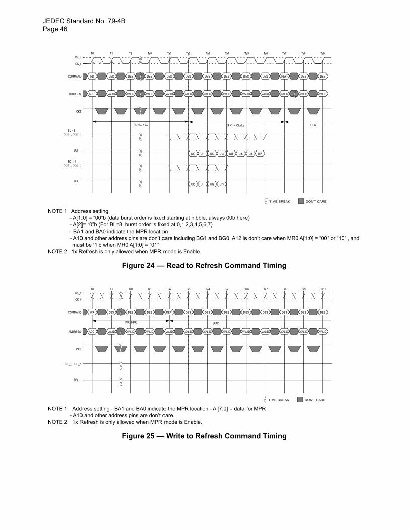
JEDEC Standard No. 79-4BPage 46
NOTE 1 Address setting - A[1:0] = “00”b (data burst order is fixed starting at nibble, always 00b here) - A[2]= “0”b (For BL=8, burst order is fixed at 0,1,2,3,4,5,6,7) - BA1 and BA0 indicate the MPR location - A10 and other address pins are don’t care including BG1 and BG0. A12 is don’t care when MR0 A[1:0] = “00” or “10” , and
must be ‘1’b when MR0 A[1:0] = “01” NOTE 2 1x Refresh is only allowed when MPR mode is Enable.
Figure 24 — Read to Refresh Command Timing
NOTE 1 Address setting - BA1 and BA0 indicate the MPR location - A [7:0] = data for MPR - A10 and other address pins are don’t care.NOTE 2 1x Refresh is only allowed when MPR mode is Enable.
Figure 25 — Write to Refresh Command Timing
DES
T1 T2 Ta3 Ta4 Ta5 Ta6Ta0 Ta9
DES DES DES
T0
DES
CK_c
CK_t
COMMAND
ADDRESS
DQS_t, DQS_c
CKE
TIME BREAK DON’T CARE
Ta1 Ta2
DESRD DES DES DES DES REF2 DES
Ta7 Ta8
VALID VALID VALID VALIDVALID VALIDADD1 VALID VALID VALID VALID VALID VALID
PL +AL + CL
DQUI7UI3 UI5UI2 UI4 UI6UI1UI0
(4 +1) + Clocks tRFC
BL = 8
DQS_t, DQS_c
DQUI3UI2UI1UI0
BC = 4
DES
T1 Ta0 Ta4 Ta5 Ta6 Ta7Ta1 Ta10
DES DES DES
T0
DES
CK_c
CK_t
COMMAND
ADDRESS
DQS_t, DQS_c
CKE
TIME BREAK DON’T CARE
Ta2 Ta3
DESWR REF2 DES DES DES DES DES
Ta8 Ta9
VALID VALID VALID VALIDVALID VALIDADD1 VALID VALID VALID VALID VALID VALID
DQ
tWR_MPR tRFC
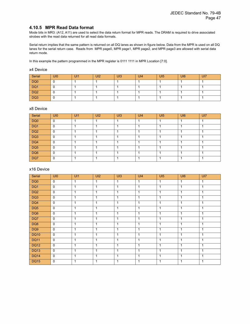
JEDEC Standard No. 79-4B Page 47
4.10.5 MPR Read Data formatMode bits in MR3: (A12, A11) are used to select the data return format for MPR reads. The DRAM is required to drive associated strobes with the read data returned for all read data formats.
Serial return implies that the same pattern is returned on all DQ lanes as shown in figure below. Data from the MPR is used on all DQ lanes for the serial return case. Reads from MPR page0, MPR page1, MPR page2, and MPR page3 are allowed with serial data return mode.
In this example the pattern programmed in the MPR register is 0111 1111 in MPR Location [7:0].
x4 Device
x8 Device
x16 Device
Serial UI0 UI1 UI2 UI3 UI4 UI5 UI6 UI7
DQ0 0 1 1 1 1 1 1 1
DQ1 0 1 1 1 1 1 1 1
DQ2 0 1 1 1 1 1 1 1
DQ3 0 1 1 1 1 1 1 1
Serial UI0 UI1 UI2 UI3 UI4 UI5 UI6 UI7
DQ0 0 1 1 1 1 1 1 1
DQ1 0 1 1 1 1 1 1 1
DQ2 0 1 1 1 1 1 1 1
DQ3 0 1 1 1 1 1 1 1
DQ4 0 1 1 1 1 1 1 1
DQ5 0 1 1 1 1 1 1 1
DQ6 0 1 1 1 1 1 1 1
DQ7 0 1 1 1 1 1 1 1
Serial UI0 UI1 UI2 UI3 UI4 UI5 UI6 UI7
DQ0 0 1 1 1 1 1 1 1
DQ1 0 1 1 1 1 1 1 1
DQ2 0 1 1 1 1 1 1 1
DQ3 0 1 1 1 1 1 1 1
DQ4 0 1 1 1 1 1 1 1
DQ5 0 1 1 1 1 1 1 1
DQ6 0 1 1 1 1 1 1 1
DQ7 0 1 1 1 1 1 1 1
DQ8 0 1 1 1 1 1 1 1
DQ9 0 1 1 1 1 1 1 1
DQ10 0 1 1 1 1 1 1 1
DQ11 0 1 1 1 1 1 1 1
DQ12 0 1 1 1 1 1 1 1
DQ13 0 1 1 1 1 1 1 1
DQ14 0 1 1 1 1 1 1 1
DQ15 0 1 1 1 1 1 1 1
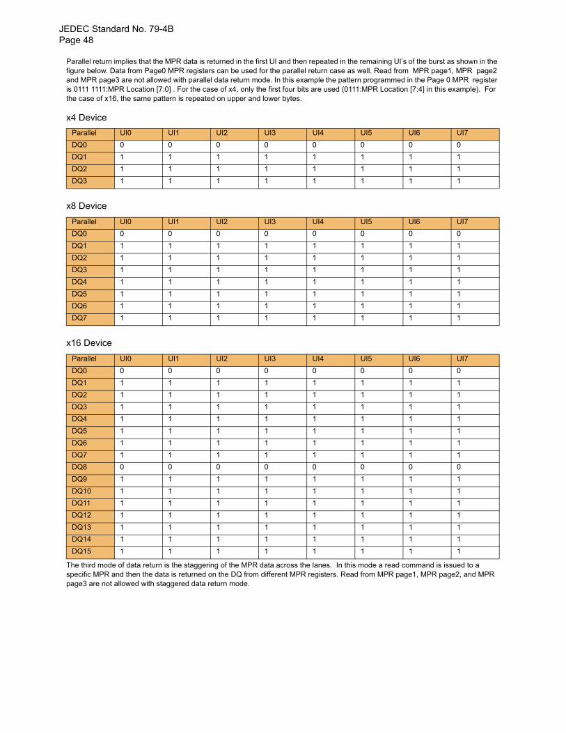
JEDEC Standard No. 79-4BPage 48
Parallel return implies that the MPR data is returned in the first UI and then repeated in the remaining UI’s of the burst as shown in the figure below. Data from Page0 MPR registers can be used for the parallel return case as well. Read from MPR page1, MPR page2 and MPR page3 are not allowed with parallel data return mode. In this example the pattern programmed in the Page 0 MPR register is 0111 1111:MPR Location [7:0] . For the case of x4, only the first four bits are used (0111:MPR Location [7:4] in this example). For the case of x16, the same pattern is repeated on upper and lower bytes.
x4 Device
x8 Device
x16 Device
The third mode of data return is the staggering of the MPR data across the lanes. In this mode a read command is issued to a specific MPR and then the data is returned on the DQ from different MPR registers. Read from MPR page1, MPR page2, and MPR page3 are not allowed with staggered data return mode.
Parallel UI0 UI1 UI2 UI3 UI4 UI5 UI6 UI7
DQ0 0 0 0 0 0 0 0 0
DQ1 1 1 1 1 1 1 1 1
DQ2 1 1 1 1 1 1 1 1
DQ3 1 1 1 1 1 1 1 1
Parallel UI0 UI1 UI2 UI3 UI4 UI5 UI6 UI7
DQ0 0 0 0 0 0 0 0 0
DQ1 1 1 1 1 1 1 1 1
DQ2 1 1 1 1 1 1 1 1
DQ3 1 1 1 1 1 1 1 1
DQ4 1 1 1 1 1 1 1 1
DQ5 1 1 1 1 1 1 1 1
DQ6 1 1 1 1 1 1 1 1
DQ7 1 1 1 1 1 1 1 1
Parallel UI0 UI1 UI2 UI3 UI4 UI5 UI6 UI7
DQ0 0 0 0 0 0 0 0 0
DQ1 1 1 1 1 1 1 1 1
DQ2 1 1 1 1 1 1 1 1
DQ3 1 1 1 1 1 1 1 1
DQ4 1 1 1 1 1 1 1 1
DQ5 1 1 1 1 1 1 1 1
DQ6 1 1 1 1 1 1 1 1
DQ7 1 1 1 1 1 1 1 1
DQ8 0 0 0 0 0 0 0 0
DQ9 1 1 1 1 1 1 1 1
DQ10 1 1 1 1 1 1 1 1
DQ11 1 1 1 1 1 1 1 1
DQ12 1 1 1 1 1 1 1 1
DQ13 1 1 1 1 1 1 1 1
DQ14 1 1 1 1 1 1 1 1
DQ15 1 1 1 1 1 1 1 1
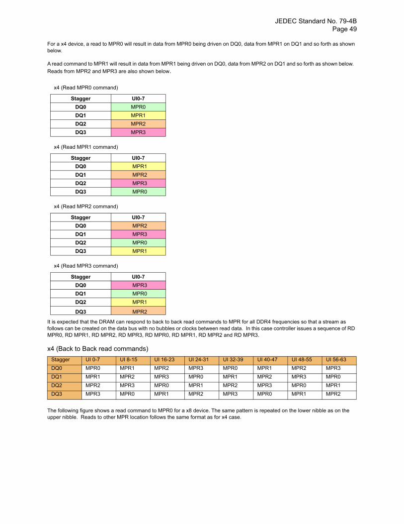
JEDEC Standard No. 79-4B Page 49
For a x4 device, a read to MPR0 will result in data from MPR0 being driven on DQ0, data from MPR1 on DQ1 and so forth as shown below.
A read command to MPR1 will result in data from MPR1 being driven on DQ0, data from MPR2 on DQ1 and so forth as shown below.
Reads from MPR2 and MPR3 are also shown below.
It is expected that the DRAM can respond to back to back read commands to MPR for all DDR4 frequencies so that a stream as follows can be created on the data bus with no bubbles or clocks between read data. In this case controller issues a sequence of RD MPR0, RD MPR1, RD MPR2, RD MPR3, RD MPR0, RD MPR1, RD MPR2 and RD MPR3.
x4 (Back to Back read commands)
The following figure shows a read command to MPR0 for a x8 device. The same pattern is repeated on the lower nibble as on the upper nibble. Reads to other MPR location follows the same format as for x4 case.
x4 (Read MPR0 command)
Stagger UI0-7
DQ0 MPR0
DQ1 MPR1
DQ2 MPR2
DQ3 MPR3
x4 (Read MPR1 command)
Stagger UI0-7
DQ0 MPR1
DQ1 MPR2
DQ2 MPR3
DQ3 MPR0
x4 (Read MPR2 command)
Stagger UI0-7
DQ0 MPR2
DQ1 MPR3
DQ2 MPR0
DQ3 MPR1
x4 (Read MPR3 command)
Stagger UI0-7
DQ0 MPR3
DQ1 MPR0
DQ2 MPR1
DQ3 MPR2
Stagger UI 0-7 UI 8-15 UI 16-23 UI 24-31 UI 32-39 UI 40-47 UI 48-55 UI 56-63
DQ0 MPR0 MPR1 MPR2 MPR3 MPR0 MPR1 MPR2 MPR3
DQ1 MPR1 MPR2 MPR3 MPR0 MPR1 MPR2 MPR3 MPR0
DQ2 MPR2 MPR3 MPR0 MPR1 MPR2 MPR3 MPR0 MPR1
DQ3 MPR3 MPR0 MPR1 MPR2 MPR3 MPR0 MPR1 MPR2
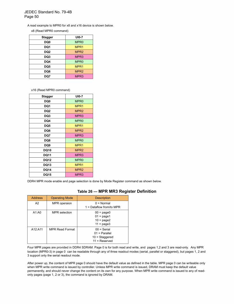
JEDEC Standard No. 79-4BPage 50
A read example to MPR0 for x8 and x16 device is shown below.
DDR4 MPR mode enable and page selection is done by Mode Register command as shown below.
Table 26 — MPR MR3 Register Definition
Four MPR pages are provided in DDR4 SDRAM. Page 0 is for both read and write, and pages 1,2 and 3 are read-only. Any MPR location (MPR0-3) in page 0 can be readable through any of three readout modes (serial, parallel or staggered), but pages 1, 2 and 3 support only the serial readout mode.
After power up, the content of MPR page 0 should have the default value as defined in the table. MPR page 0 can be writeable only when MPR write command is issued by controller. Unless MPR write command is issued, DRAM must keep the default value permanently, and should never change the content on its own for any purpose. When MPR write command is issued to any of read-only pages (page 1, 2 or 3), the command is ignored by DRAM.
x8 (Read MPR0 command)
Stagger UI0-7
DQ0 MPR0
DQ1 MPR1
DQ2 MPR2
DQ3 MPR3
DQ4 MPR0
DQ5 MPR1
DQ6 MPR2
DQ7 MPR3
x16 (Read MPR0 command)
Stagger UI0-7
DQ0 MPR0
DQ1 MPR1
DQ2 MPR2
DQ3 MPR3
DQ4 MPR0
DQ5 MPR1
DQ6 MPR2
DQ7 MPR3
DQ8 MPR0
DQ9 MPR1
DQ10 MPR2
DQ11 MPR3
DQ12 MPR0
DQ13 MPR1
DQ14 MPR2
DQ15 MPR3
Address Operating Mode Description
A2 MPR operaion 0 = Normal1 = Dataflow from/to MPR
A1:A0 MPR selection 00 = page001 = page110 = page211 = page3
A12:A11 MPR Read Format 00 = Serial01 = Parallel
10 = Staggered11 = Reserved
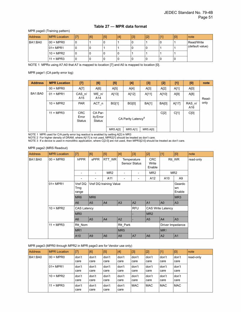
JEDEC Standard No. 79-4B Page 51
Table 27 — MPR data formatMPR page0 (Training pattern)
NOTE 1 MPRx using A7:A0 that A7 is mapped to location [7] and A0 is mapped to location [0].
MPR page1 (CA parity error log)
NOTE 1 MPR used for C/A parity error log readout is enabled by setting A[2] in MR3NOTE 2 For higher density of DRAM, where A[17] is not used, MPR2[1] should be treated as don’t care.NOTE 3 If a device is used in monolithic application, where C[2:0] are not used, then MPR3[2:0] should be treated as don’t care.
MPR page2 (MRS Readout)
MPR page3 (MPR0 through MPR2 in MPR page3 are for Vendor use only)
Address MPR Location [7] [6] [5] [4] [3] [2] [1] [0] note
BA1:BA0 00 = MPR0 0 1 0 1 0 1 0 1 Read/Write(default value)01= MPR1 0 0 1 1 0 0 1 1
10 = MPR2 0 0 0 0 1 1 1 1
11 = MPR3 0 0 0 0 0 0 0 0
Address MPR Location [7] [6] [5] [4] [3] [2] [1] [0] note
BA1:BA0
00 = MPR0 A[7] A[6] A[5] A[4] A[3] A[2] A[1] A[0]
Read-only
01 = MPR1 CAS_n/A15
WE_n/A14
A[13] A[12] A[11] A[10] A[9] A[8]
10 = MPR2 PAR ACT_n BG[1] BG[0] BA[1] BA[0] A[17] RAS_n/A16
11 = MPR3 CRC Error
Status
CA Par-ity Error Status
CA Parity Latency4
C[2] C[1] C[0]
MR5.A[2] MR5.A[1] MR5.A[0]
Address MPR Location [7] [6] [5] [4] [3] [2] [1] [0] note
BA1:BA0 00 = MPR0 hPPR sPPR RTT_WR TemperatureSensor Status
CRC Write
Enable
Rtt_WR read-only
- - MR2 - - MR2 MR2
- - A11 - - A12 A10 A9
01= MPR1 Vref DQ Trng range
Vref DQ training Value Geardown Enable
MR6 MR6 MR3
A6 A5 A4 A3 A2 A1 A0 A3
10 = MPR2 CAS Latency RFU CAS Write Latency
MR0 - MR2
A6 A5 A4 A2 - A5 A4 A3
11 = MPR3 Rtt_Nom Rtt_Park Driver Impedance
MR1 MR5 MR1
A10 A9 A6 A8 A7 A6 A2 A1
Address MPR Location [7] [6] [5] [4] [3] [2] [1] [0] note
BA1:BA0 00 = MPR0 don’tcare
don’tcare
don’tcare
don’tcare
don’tcare
don’tcare
don’tcare
don’tcare
read-only
01= MPR1 don’tcare
don’tcare
don’tcare
don’tcare
don’tcare
don’tcare
don’tcare
don’tcare
10 = MPR2 don’tcare
don’tcare
don’tcare
don’tcare
don’tcare
don’tcare
don’tcare
don’tcare
11 = MPR3 don’tcare
don’tcare
don’tcare
don’tcare
MAC MAC MAC MAC
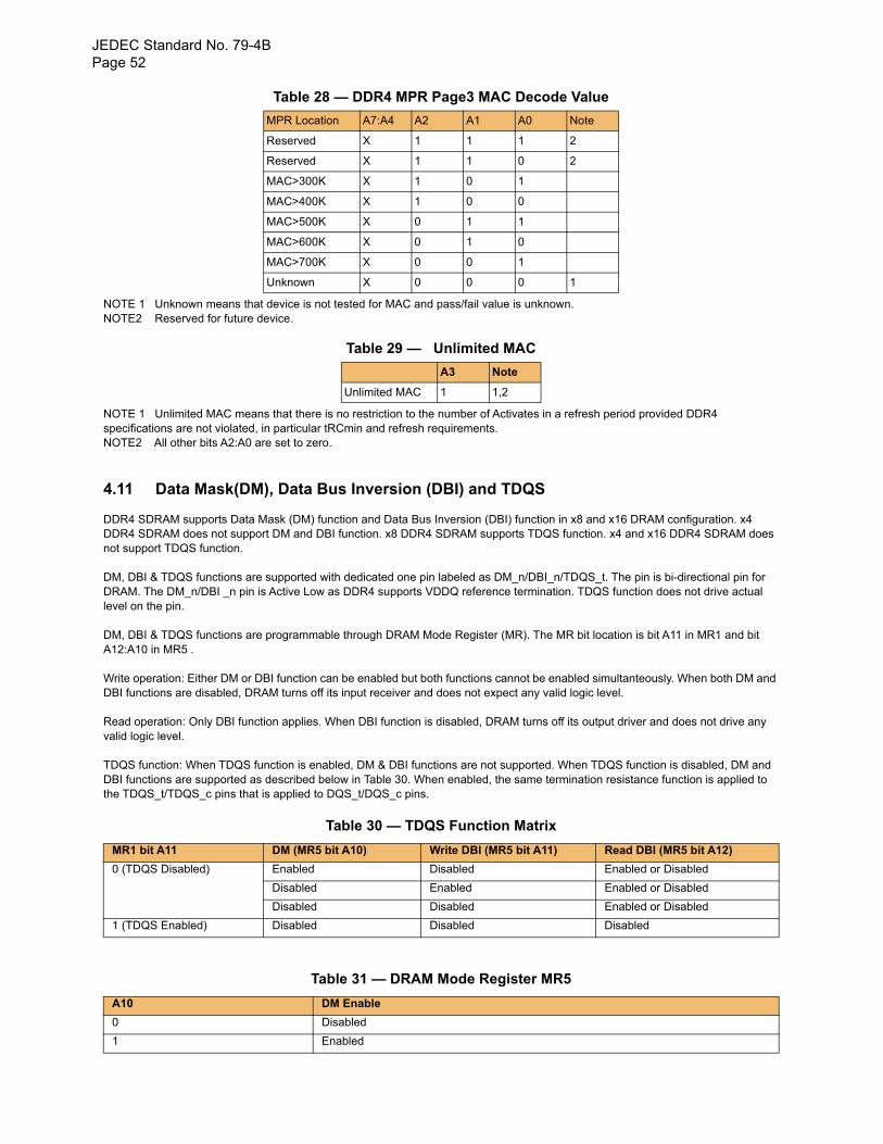
JEDEC Standard No. 79-4BPage 52
Table 28 — DDR4 MPR Page3 MAC Decode Value
NOTE 1 Unknown means that device is not tested for MAC and pass/fail value is unknown.NOTE2 Reserved for future device.
Table 29 — Unlimited MAC
NOTE 1 Unlimited MAC means that there is no restriction to the number of Activates in a refresh period provided DDR4 specifications are not violated, in particular tRCmin and refresh requirements.NOTE2 All other bits A2:A0 are set to zero.
4.11 Data Mask(DM), Data Bus Inversion (DBI) and TDQS
DDR4 SDRAM supports Data Mask (DM) function and Data Bus Inversion (DBI) function in x8 and x16 DRAM configuration. x4 DDR4 SDRAM does not support DM and DBI function. x8 DDR4 SDRAM supports TDQS function. x4 and x16 DDR4 SDRAM does not support TDQS function.
DM, DBI & TDQS functions are supported with dedicated one pin labeled as DM_n/DBI_n/TDQS_t. The pin is bi-directional pin for DRAM. The DM_n/DBI _n pin is Active Low as DDR4 supports VDDQ reference termination. TDQS function does not drive actual level on the pin.
DM, DBI & TDQS functions are programmable through DRAM Mode Register (MR). The MR bit location is bit A11 in MR1 and bit A12:A10 in MR5 .
Write operation: Either DM or DBI function can be enabled but both functions cannot be enabled simultanteously. When both DM and DBI functions are disabled, DRAM turns off its input receiver and does not expect any valid logic level.
Read operation: Only DBI function applies. When DBI function is disabled, DRAM turns off its output driver and does not drive any valid logic level.
TDQS function: When TDQS function is enabled, DM & DBI functions are not supported. When TDQS function is disabled, DM and DBI functions are supported as described below in Table 30. When enabled, the same termination resistance function is applied to the TDQS_t/TDQS_c pins that is applied to DQS_t/DQS_c pins.
Table 30 — TDQS Function Matrix
Table 31 — DRAM Mode Register MR5
MPR Location A7:A4 A2 A1 A0 Note
Reserved X 1 1 1 2
Reserved X 1 1 0 2
MAC>300K X 1 0 1
MAC>400K X 1 0 0
MAC>500K X 0 1 1
MAC>600K X 0 1 0
MAC>700K X 0 0 1
Unknown X 0 0 0 1
A3 Note
Unlimited MAC 1 1,2
MR1 bit A11 DM (MR5 bit A10) Write DBI (MR5 bit A11) Read DBI (MR5 bit A12)
0 (TDQS Disabled) Enabled Disabled Enabled or Disabled
Disabled Enabled Enabled or Disabled
Disabled Disabled Enabled or Disabled
1 (TDQS Enabled) Disabled Disabled Disabled
A10 DM Enable
0 Disabled
1 Enabled
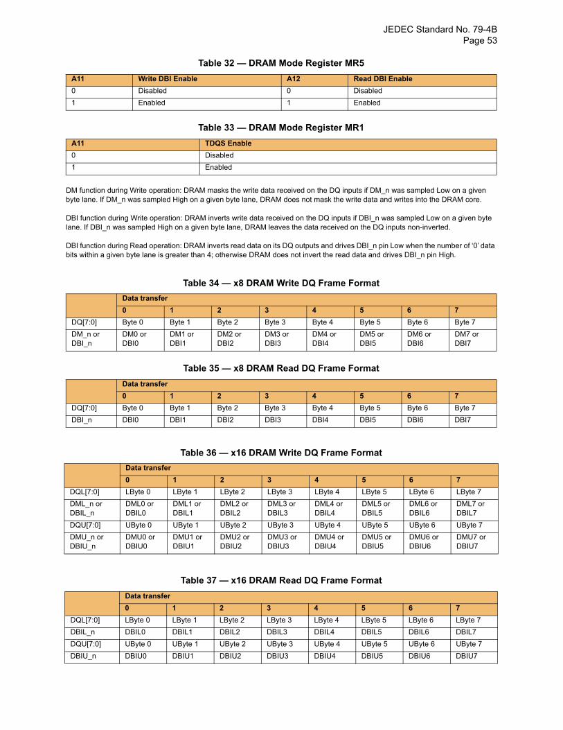
JEDEC Standard No. 79-4B Page 53
Table 32 — DRAM Mode Register MR5
Table 33 — DRAM Mode Register MR1
DM function during Write operation: DRAM masks the write data received on the DQ inputs if DM_n was sampled Low on a given byte lane. If DM_n was sampled High on a given byte lane, DRAM does not mask the write data and writes into the DRAM core.
DBI function during Write operation: DRAM inverts write data received on the DQ inputs if DBI_n was sampled Low on a given byte lane. If DBI_n was sampled High on a given byte lane, DRAM leaves the data received on the DQ inputs non-inverted.
DBI function during Read operation: DRAM inverts read data on its DQ outputs and drives DBI_n pin Low when the number of ‘0’ data bits within a given byte lane is greater than 4; otherwise DRAM does not invert the read data and drives DBI_n pin High.
Table 34 — x8 DRAM Write DQ Frame Format
Table 35 — x8 DRAM Read DQ Frame Format
Table 36 — x16 DRAM Write DQ Frame Format
Table 37 — x16 DRAM Read DQ Frame Format
A11 Write DBI Enable A12 Read DBI Enable
0 Disabled 0 Disabled
1 Enabled 1 Enabled
A11 TDQS Enable
0 Disabled
1 Enabled
Data transfer
0 1 2 3 4 5 6 7
DQ[7:0] Byte 0 Byte 1 Byte 2 Byte 3 Byte 4 Byte 5 Byte 6 Byte 7
DM_n or DBI_n
DM0 or DBI0
DM1 or DBI1
DM2 or DBI2
DM3 or DBI3
DM4 or DBI4
DM5 or DBI5
DM6 or DBI6
DM7 or DBI7
Data transfer
0 1 2 3 4 5 6 7
DQ[7:0] Byte 0 Byte 1 Byte 2 Byte 3 Byte 4 Byte 5 Byte 6 Byte 7
DBI_n DBI0 DBI1 DBI2 DBI3 DBI4 DBI5 DBI6 DBI7
Data transfer
0 1 2 3 4 5 6 7
DQL[7:0] LByte 0 LByte 1 LByte 2 LByte 3 LByte 4 LByte 5 LByte 6 LByte 7
DML_n or DBIL_n
DML0 or DBIL0
DML1 or DBIL1
DML2 or DBIL2
DML3 or DBIL3
DML4 or DBIL4
DML5 or DBIL5
DML6 or DBIL6
DML7 or DBIL7
DQU[7:0] UByte 0 UByte 1 UByte 2 UByte 3 UByte 4 UByte 5 UByte 6 UByte 7
DMU_n or DBIU_n
DMU0 or DBIU0
DMU1 or DBIU1
DMU2 or DBIU2
DMU3 or DBIU3
DMU4 or DBIU4
DMU5 or DBIU5
DMU6 or DBIU6
DMU7 or DBIU7
Data transfer
0 1 2 3 4 5 6 7
DQL[7:0] LByte 0 LByte 1 LByte 2 LByte 3 LByte 4 LByte 5 LByte 6 LByte 7
DBIL_n DBIL0 DBIL1 DBIL2 DBIL3 DBIL4 DBIL5 DBIL6 DBIL7
DQU[7:0] UByte 0 UByte 1 UByte 2 UByte 3 UByte 4 UByte 5 UByte 6 UByte 7
DBIU_n DBIU0 DBIU1 DBIU2 DBIU3 DBIU4 DBIU5 DBIU6 DBIU7
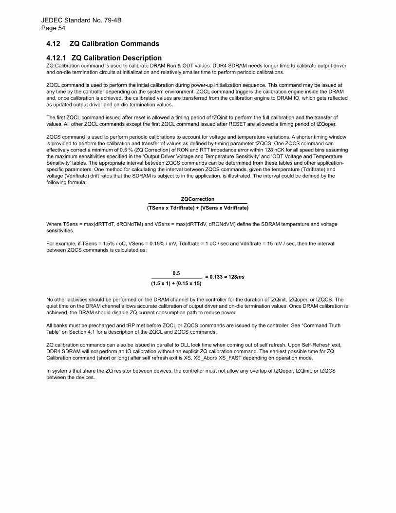
JEDEC Standard No. 79-4BPage 54
4.12 ZQ Calibration Commands
4.12.1 ZQ Calibration DescriptionZQ Calibration command is used to calibrate DRAM Ron & ODT values. DDR4 SDRAM needs longer time to calibrate output driver and on-die termination circuits at initialization and relatively smaller time to perform periodic calibrations.
ZQCL command is used to perform the initial calibration during power-up initialization sequence. This command may be issued at any time by the controller depending on the system environment. ZQCL command triggers the calibration engine inside the DRAM and, once calibration is achieved, the calibrated values are transferred from the calibration engine to DRAM IO, which gets reflected as updated output driver and on-die termination values.
The first ZQCL command issued after reset is allowed a timing period of tZQinit to perform the full calibration and the transfer of values. All other ZQCL commands except the first ZQCL command issued after RESET are allowed a timing period of tZQoper.
ZQCS command is used to perform periodic calibrations to account for voltage and temperature variations. A shorter timing window is provided to perform the calibration and transfer of values as defined by timing parameter tZQCS. One ZQCS command can effectively correct a minimum of 0.5 % (ZQ Correction) of RON and RTT impedance error within 128 nCK for all speed bins assuming the maximum sensitivities specified in the ‘Output Driver Voltage and Temperature Sensitivity’ and ‘ODT Voltage and Temperature Sensitivity’ tables. The appropriate interval between ZQCS commands can be determined from these tables and other application-specific parameters. One method for calculating the interval between ZQCS commands, given the temperature (Tdriftrate) and voltage (Vdriftrate) drift rates that the SDRAM is subject to in the application, is illustrated. The interval could be defined by the following formula:
Where TSens = max(dRTTdT, dRONdTM) and VSens = max(dRTTdV, dRONdVM) define the SDRAM temperature and voltage sensitivities.
For example, if TSens = 1.5% / oC, VSens = 0.15% / mV, Tdriftrate = 1 oC / sec and Vdriftrate = 15 mV / sec, then the interval between ZQCS commands is calculated as:
No other activities should be performed on the DRAM channel by the controller for the duration of tZQinit, tZQoper, or tZQCS. The quiet time on the DRAM channel allows accurate calibration of output driver and on-die termination values. Once DRAM calibration is achieved, the DRAM should disable ZQ current consumption path to reduce power.
All banks must be precharged and tRP met before ZQCL or ZQCS commands are issued by the controller. See “Command Truth Table” on Section 4.1 for a description of the ZQCL and ZQCS commands.
ZQ calibration commands can also be issued in parallel to DLL lock time when coming out of self refresh. Upon Self-Refresh exit, DDR4 SDRAM will not perform an IO calibration without an explicit ZQ calibration command. The earliest possible time for ZQ Calibration command (short or long) after self refresh exit is XS, XS_Abort/ XS_FAST depending on operation mode.
In systems that share the ZQ resistor between devices, the controller must not allow any overlap of tZQoper, tZQinit, or tZQCS between the devices.
ZQCorrection
(TSens x Tdriftrate) + (VSens x Vdriftrate)
(1.5 x 1) + (0.15 x 15)
0.5= 0.133 128ms~~
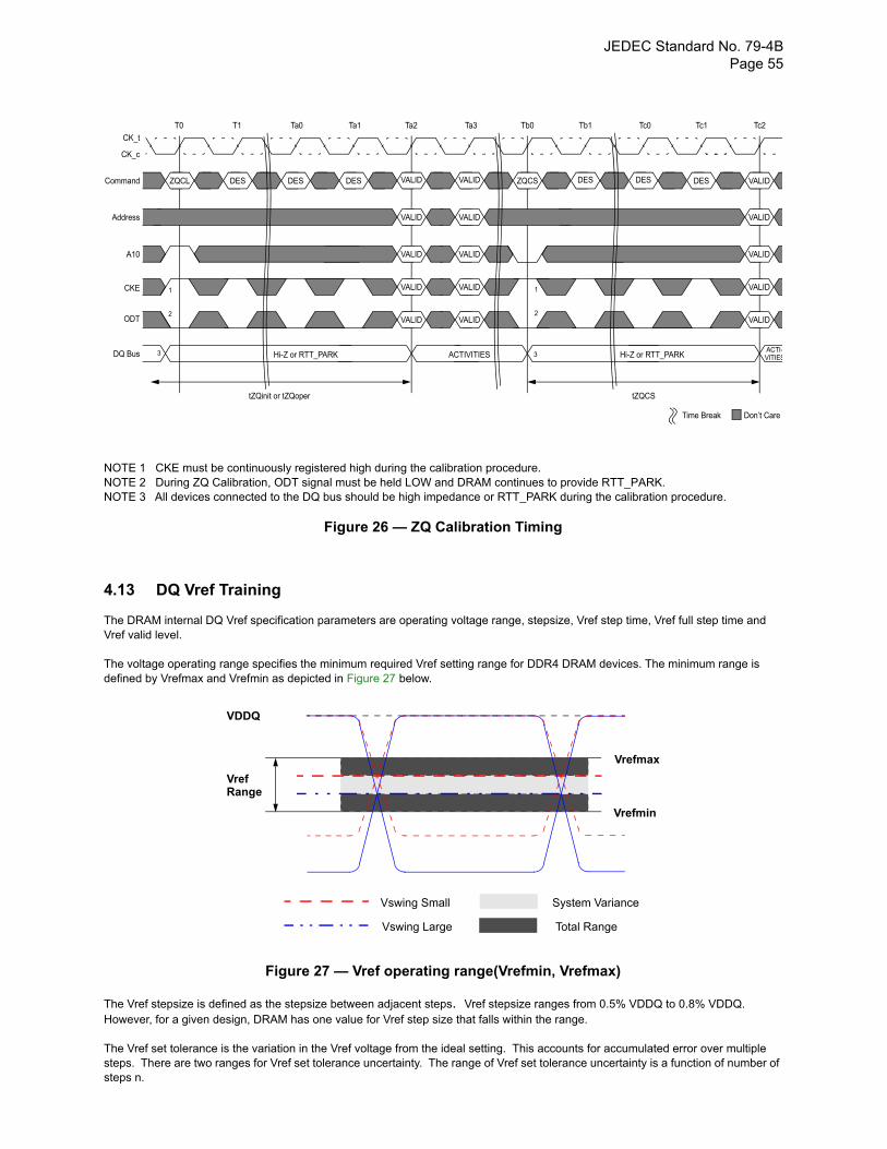
JEDEC Standard No. 79-4B Page 55
NOTE 1 CKE must be continuously registered high during the calibration procedure.NOTE 2 During ZQ Calibration, ODT signal must be held LOW and DRAM continues to provide RTT_PARK. NOTE 3 All devices connected to the DQ bus should be high impedance or RTT_PARK during the calibration procedure.
Figure 26 — ZQ Calibration Timing
4.13 DQ Vref Training
The DRAM internal DQ Vref specification parameters are operating voltage range, stepsize, Vref step time, Vref full step time and Vref valid level.
The voltage operating range specifies the minimum required Vref setting range for DDR4 DRAM devices. The minimum range is defined by Vrefmax and Vrefmin as depicted in Figure 27 below.
Figure 27 — Vref operating range(Vrefmin, Vrefmax)
The Vref stepsize is defined as the stepsize between adjacent steps. Vref stepsize ranges from 0.5% VDDQ to 0.8% VDDQ. However, for a given design, DRAM has one value for Vref step size that falls within the range.
The Vref set tolerance is the variation in the Vref voltage from the ideal setting. This accounts for accumulated error over multiple steps. There are two ranges for Vref set tolerance uncertainty. The range of Vref set tolerance uncertainty is a function of number of steps n.
CK_t
CK_c
T0 Ta0 Ta2 Tb0 Tb1 Tc1 Tc2
ZQCL DES DES DES VALID VALID ZQCS DES DES DES VALIDCommand
VALID VALIDAddress
Time Break Don’t Care
A10
DQ Bus
T1 Ta1 Ta3 Tc0
VALID
VALID VALID VALID
VALID VALID VALIDCKE
VALID VALID VALIDODT
Hi-Z or RTT_PARK ACTIVITIESACTI-VITIESHi-Z or RTT_PARK
tZQinit or tZQoper tZQCS
1
2
3
1
2
3
VDDQ
VrefRange
Vrefmax
Vrefmin
Vswing Small
Vswing Large
System Variance
Total Range
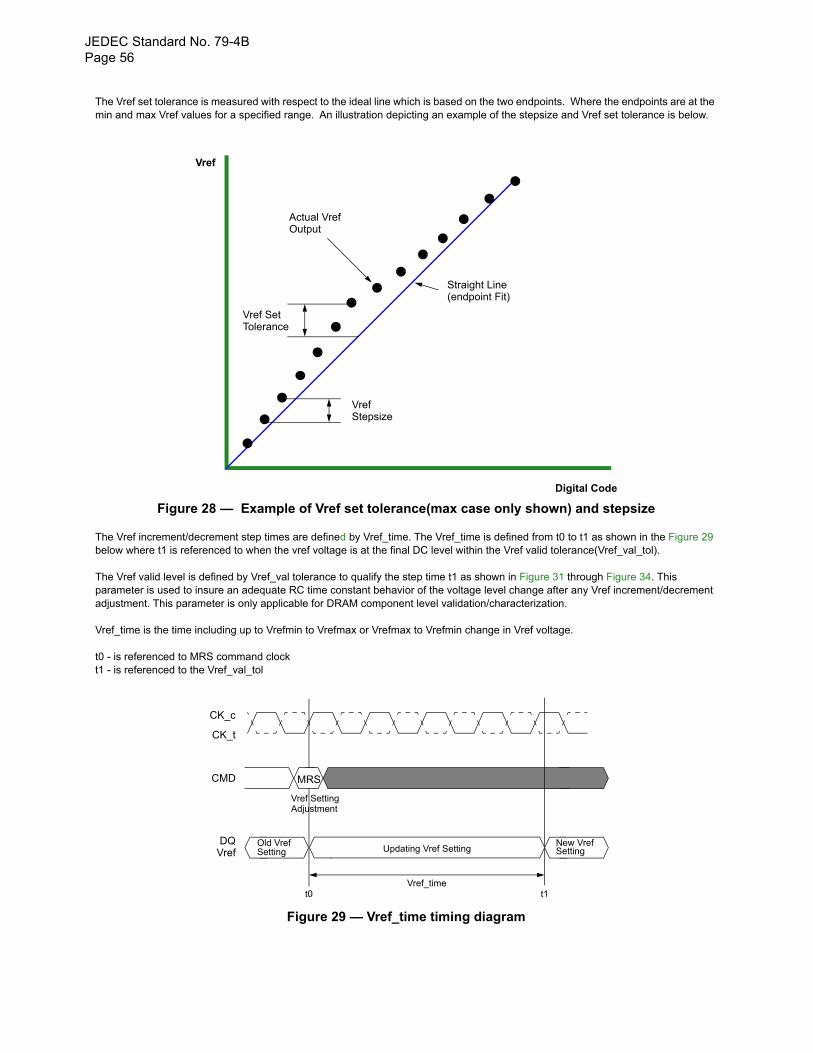
JEDEC Standard No. 79-4BPage 56
The Vref set tolerance is measured with respect to the ideal line which is based on the two endpoints. Where the endpoints are at the min and max Vref values for a specified range. An illustration depicting an example of the stepsize and Vref set tolerance is below.
Figure 28 — Example of Vref set tolerance(max case only shown) and stepsize
The Vref increment/decrement step times are defined by Vref_time. The Vref_time is defined from t0 to t1 as shown in the Figure 29 below where t1 is referenced to when the vref voltage is at the final DC level within the Vref valid tolerance(Vref_val_tol).
The Vref valid level is defined by Vref_val tolerance to qualify the step time t1 as shown in Figure 31 through Figure 34. This parameter is used to insure an adequate RC time constant behavior of the voltage level change after any Vref increment/decrement adjustment. This parameter is only applicable for DRAM component level validation/characterization.
Vref_time is the time including up to Vrefmin to Vrefmax or Vrefmax to Vrefmin change in Vref voltage.
t0 - is referenced to MRS command clockt1 - is referenced to the Vref_val_tol
Figure 29 — Vref_time timing diagram
Vref
Digital Code
Straight Line(endpoint Fit)
Actual VrefOutput
Vref SetTolerance
VrefStepsize
CK_t
CMD
DQ
CK_c
MRS
VrefOld VrefSetting
Vref SettingAdjustment
New VrefSettingUpdating Vref Setting
t0 t1Vref_time
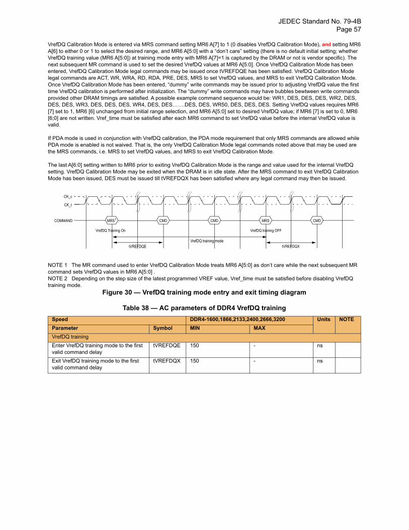
JEDEC Standard No. 79-4B Page 57
VrefDQ Calibration Mode is entered via MRS command setting MR6 A[7] to 1 (0 disables VrefDQ Calibration Mode), and setting MR6A[6] to either 0 or 1 to select the desired range, and MR6 A[5:0] with a “don’t care” setting (there is no default initial setting; whetherVrefDQ training value (MR6 A[5:0]) at training mode entry with MR6 A[7]=1 is captured by the DRAM or not is vendor specific). Thenext subsequent MR command is used to set the desired VrefDQ values at MR6 A[5:0]. Once VrefDQ Calibration Mode has been entered, VrefDQ Calibration Mode legal commands may be issued once tVREFDQE has been satisfied. VrefDQ Calibration Mode legal commands are ACT, WR, WRA, RD, RDA, PRE, DES, MRS to set VrefDQ values, and MRS to exit VrefDQ Calibration Mode. Once VrefDQ Calibration Mode has been entered, “dummy” write commands may be issued prior to adjusting VrefDQ value the first time VrefDQ calibration is performed after initialization. The “dummy” write commands may have bubbles bewtween write commands provided other DRAM timings are satisfied. A possible example command sequence would be: WR1, DES, DES, DES, WR2, DES, DES, DES, WR3, DES, DES, DES, WR4, DES, DES…….DES, DES, WR50, DES, DES, DES. Setting VrefDQ values requires MR6 [7] set to 1, MR6 [6] unchanged from initial range selection, and MR6 A[5:0] set to desired VrefDQ value; if MR6 [7] is set to 0, MR6 [6;0] are not written. Vref_time must be satisfied after each MR6 command to set VrefDQ value before the internal VrefDQ value is valid.
If PDA mode is used in conjunction with VrefDQ calibration, the PDA mode requirement that only MRS commands are allowed whilePDA mode is enabled is not waived. That is, the only VrefDQ Calibration Mode legal commands noted above that may be used arethe MRS commands, i.e. MRS to set VrefDQ values, and MRS to exit VrefDQ Calibration Mode.
The last A[6:0] setting written to MR6 prior to exiting VrefDQ Calibration Mode is the range and value used for the internal VrefDQ setting. VrefDQ Calibration Mode may be exited when the DRAM is in idle state. After the MRS command to exit VrefDQ CalibrationMode has been issued, DES must be issued till tVREFDQX has been satisfied where any legal command may then be issued.
NOTE 1 The MR command used to enter VrefDQ Calibration Mode treats MR6 A[5:0] as don’t care while the next subsequent MR command sets VrefDQ values in MR6 A[5:0] .NOTE 2 Depending on the step size of the latest programmed VREF value, Vref_time must be satisfied before disabling VrefDQ training mode.
Figure 30 — VrefDQ training mode entry and exit timing diagram
Table 38 — AC parameters of DDR4 VrefDQ training
Speed DDR4-1600,1866,2133,2400,2666,3200 Units NOTE
Parameter Symbol MIN MAX
VrefDQ training
Enter VrefDQ training mode to the first valid command delay
tVREFDQE 150 - ns
Exit VrefDQ training mode to the first valid command delay
tVREFDQX 150 - ns
CMD CMD CMDMRS1
CK_c
CK_t
COMMAND MRS
tVREFDQE
VrefDQ Training On VrefDQ training OFF
tVREFDQXVrefDQ training mode
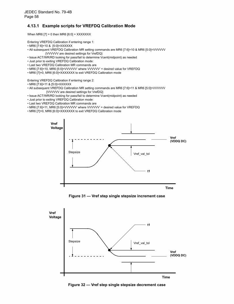
JEDEC Standard No. 79-4BPage 58
4.13.1 Example scripts for VREFDQ Calibration Mode
When MR6 [7] = 0 then MR6 [6:0] = XXXXXXX
Entering VREFDQ Calibration if entering range 1:• MR6 [7:6]=10 & [5:0]=XXXXXX• All subsequent VREFDQ Calibration MR setting commands are MR6 [7:6]=10 & MR6 [5:0]=VVVVVV {VVVVVV are desired settings for VrefDQ}• Issue ACT/WR/RD looking for pass/fail to determine Vcent(midpoint) as needed• Just prior to exiting VREFDQ Calibration mode:• Last two VREFDQ Calibration MR commands are• MR6 [7:6]=10, MR6 [5:0]=VVVVVV’ where VVVVVV’ = desired value for VREFDQ• MR6 [7]=0, MR6 [6:0]=XXXXXXX to exit VREFDQ Calibration mode
Entering VREFDQ Calibration if entering range 2:• MR6 [7:6]=11 & [5:0]=XXXXXX• All subsequent VREFDQ Calibration MR setting commands are MR6 [7:6]=11 & MR6 [5:0]=VVVVVV {VVVVVV are desired settings for VrefDQ}• Issue ACT/WR/RD looking for pass/fail to determine Vcent(midpoint) as needed• Just prior to exiting VREFDQ Calibration mode:• Last two VREFDQ Calibration MR commands are• MR6 [7:6]=11, MR6 [5:0]=VVVVVV’ where VVVVVV’ = desired value for VREFDQ• MR6 [7]=0, MR6 [6:0]=XXXXXXX to exit VREFDQ Calibration mode
Figure 31 — Vref step single stepsize increment case
Figure 32 — Vref step single stepsize decrement case
Stepsize Vref_val_tol
Vref(VDDQ DC)
t1
VrefVoltage
Time
Stepsize Vref_val_tol
Vref(VDDQ DC)
t1
VrefVoltage
Time
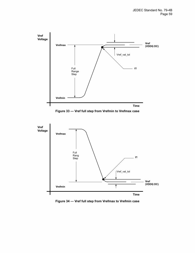
JEDEC Standard No. 79-4B Page 59
Figure 33 — Vref full step from Vrefmin to Vrefmax case
Figure 34 — Vref full step from Vrefmax to Vrefmin case
Full
Vref_val_tol
Vref(VDDQ DC)
t1
VrefVoltage
RangeStep
Vrefmax
Vrefmin
Time
Step
Vref_val_tol
Vref(VDDQ DC)
t1
VrefVoltage
RangFull
Vrefmax
Vrefmin
Time
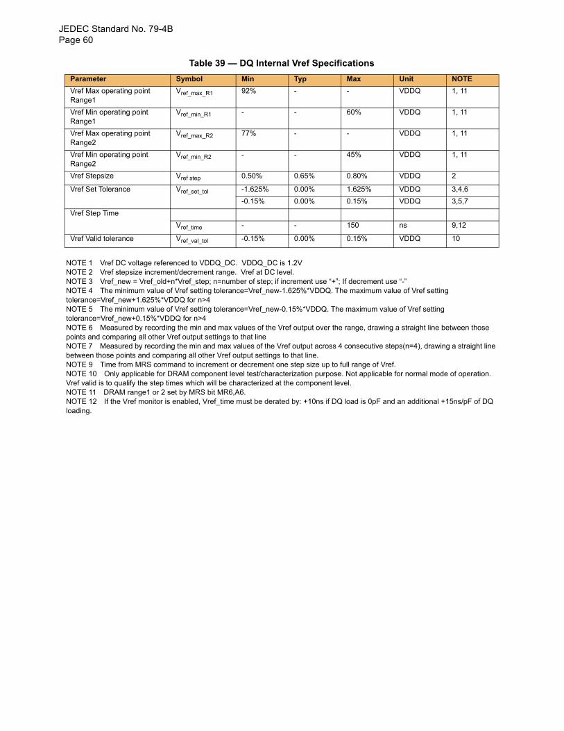
JEDEC Standard No. 79-4BPage 60
Table 39 — DQ Internal Vref Specifications
NOTE 1 Vref DC voltage referenced to VDDQ_DC. VDDQ_DC is 1.2VNOTE 2 Vref stepsize increment/decrement range. Vref at DC level.NOTE 3 Vref_new = Vref_old+n*Vref_step; n=number of step; if increment use “+”; If decrement use “-”NOTE 4 The minimum value of Vref setting tolerance=Vref_new-1.625%*VDDQ. The maximum value of Vref setting tolerance=Vref_new+1.625%*VDDQ for n>4NOTE 5 The minimum value of Vref setting tolerance=Vref_new-0.15%*VDDQ. The maximum value of Vref setting tolerance=Vref_new+0.15%*VDDQ for n>4NOTE 6 Measured by recording the min and max values of the Vref output over the range, drawing a straight line between those points and comparing all other Vref output settings to that lineNOTE 7 Measured by recording the min and max values of the Vref output across 4 consecutive steps(n=4), drawing a straight line between those points and comparing all other Vref output settings to that line. NOTE 9 Time from MRS command to increment or decrement one step size up to full range of Vref.NOTE 10 Only applicable for DRAM component level test/characterization purpose. Not applicable for normal mode of operation. Vref valid is to qualify the step times which will be characterized at the component level.NOTE 11 DRAM range1 or 2 set by MRS bit MR6,A6.NOTE 12 If the Vref monitor is enabled, Vref_time must be derated by: +10ns if DQ load is 0pF and an additional +15ns/pF of DQ loading.
Parameter Symbol Min Typ Max Unit NOTE
Vref Max operating point Range1
Vref_max_R1 92% - - VDDQ 1, 11
Vref Min operating point Range1
Vref_min_R1 - - 60% VDDQ 1, 11
Vref Max operating point Range2
Vref_max_R2 77% - - VDDQ 1, 11
Vref Min operating point Range2
Vref_min_R2 - - 45% VDDQ 1, 11
Vref Stepsize Vref step 0.50% 0.65% 0.80% VDDQ 2
Vref Set Tolerance Vref_set_tol -1.625% 0.00% 1.625% VDDQ 3,4,6
-0.15% 0.00% 0.15% VDDQ 3,5,7
Vref Step Time
Vref_time - - 150 ns 9,12
Vref Valid tolerance Vref_val_tol -0.15% 0.00% 0.15% VDDQ 10
JEDEC Standard No. 79-4B Page 61
4.14 Per DRAM Addressability
DDR4 allows programmability of a given device on a rank. As an example, this feature can be used to program different ODT or Vref values on DRAM devices on a given rank.
1. Before entering ‘per DRAM addressability (PDA)’ mode, the write leveling is required.
2. Before entering ‘per DRAM addressability (PDA)’ mode, the following Mode Register setting is possible. - RTT_PARK MR5 {A8:A6} = Enable - RTT_NOM MR1 {A10:A9:A8} = Enable
3. Enable ‘per DRAM addressability (PDA)’ mode using MR3 bit “A4=1”.
4. In the ‘per DRAM addressability’ mode, all MRS command is qualified with DQ0 for x4 and x8, and DQL0 for x16. DRAM captures DQ0 for x4 and x8, and DQL0 for x16 by using DQS_c and DQS_t for x4 and x8, DQSL_c and DQSL_t for x16 signals as shown Figure 35. If the value on DQ0 for x4 and x8, and DQL0 for x16 is 0 then the DRAM executes the MRS command. If the value on DQ0 is 1, then the DRAM ignores the MRS command. The controller can choose to drive all the DQ bits.
5. Program the desired devices and mode registers using MRS command and DQ0 for x4 and x8, and DQL0 for x16.
6. In the ‘per DRAM addressability’ mode, only MRS commands are allowed.
7. The mode register set command cycle time at PDA mode, AL + CWL + BL/2 - 0.5tCK + tMRD_PDA + (PL) is required to complete the write operation to the mode register and is the minimum time required between two MRS commands shown in Figure 35.
8. Remove the DRAM from ‘per DRAM addressability’ mode by setting MR3 bit “A4=0”. (This command will require DQ0=0 for x4 and x8, and DQL0 for x16 which shown in Figure 36.
NOTE Removing a DRAM from per DRAM addressability mode will require programming the entire MR3 when the MRS command is issued. This may impact some per DRAM values programmed within a rank as the exit command is sent to the rank. In order to avoid such a case the PDA Enable/Disable Control bit is located in a mode register that does not have any ‘per DRAM addressability’ mode controls). In per DRAM addressability mode, DRAM captures DQ0 for x4 and x8, and DQL0 for x16 using DQS_t and DQS_c for x4 and x8, DQSL_c and DQSL_t for x16 like normal write operation. However, Dynamic ODT is not supported. So extra care required for the ODT setting. If RTT_NOM MR1 {A10:A9:A8} = Enable, DDR4 SDRAM data termination need to be controlled by ODT pin and apply the same timing parameters as defined in Direct ODT function that shown in Table 40. VrefDQ value must be set to either its midpoint or Vcent_DQ(midpoint) in order to capture DQ0 or DQL0 low level for entering PDA mode.
Table 40 — Applied ODT Timing Parameter to PDA Mode
Symbol Parameter
DODTLon Direct ODT turn on latency
DODTLoff Direct ODT turn off latency
tADC RTT change timing skew
tAONAS Asynchronous RTT_NOM turn-on delay
tAOFAS Asynchronous RTT_NOM turn-off delay
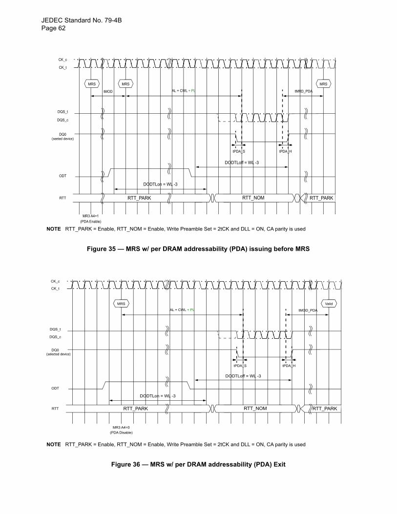
JEDEC Standard No. 79-4BPage 62
NOTE RTT_PARK = Enable, RTT_NOM = Enable, Write Preamble Set = 2tCK and DLL = ON, CA parity is used
Figure 35 — MRS w/ per DRAM addressability (PDA) issuing before MRS
NOTE RTT_PARK = Enable, RTT_NOM = Enable, Write Preamble Set = 2tCK and DLL = ON, CA parity is used
Figure 36 — MRS w/ per DRAM addressability (PDA) Exit
CK_c
CK_t
DQS_t
DQS_c
DODTLoff = WL -3
MRS MRS
MR3 A4=1
(PDA Enable)
MRS
tMOD AL + CWL + PL tMRD_PDA
tPDA_S tPDA_H
DODTLon = WL -3
RTT_PARK RTT_NOM RTT_PARK
DQ0
ODT
RTT
(seeted device)
CK_c
CK_t
DQS_t
DQS_c
DODTLoff = WL -3
MRS Valid
AL + CWL + PL tMOD_PDA
tPDA_S tPDA_H
DODTLon = WL -3
RTT_PARK RTT_NOM RTT_PARK
DQ0
ODT
RTT
MR3 A4=0
(PDA Disable)
(selected device)
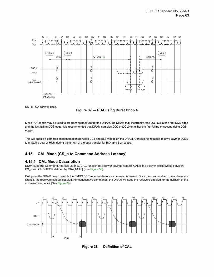
JEDEC Standard No. 79-4B Page 63
NOTE CA parity is used.Figure 37 — PDA using Burst Chop 4
Since PDA mode may be used to program optimal Vref for the DRAM, the DRAM may incorrectly read DQ level at the first DQS edge and the last falling DQS edge. It is recommended that DRAM samples DQ0 or DQL0 on either the first falling or second rising DQS edges.
This will enable a common implementation between BC4 and BL8 modes on the DRAM. Controller is required to drive DQ0 or DQL0 to a ‘Stable Low or High’ during the length of the data transfer for BC4 and BL8 cases.
4.15 CAL Mode (CS_n to Command Address Latency)
4.15.1 CAL Mode Description DDR4 supports Command Address Latency, CAL, function as a power savings feature. CAL is the delay in clock cycles between CS_n and CMD/ADDR defined by MR4[A8:A6] (See Figure 38).
CAL gives the DRAM time to enable the CMD/ADDR receivers before a command is issued. Once the command and the address are latched, the receivers can be disabled. For consecutive commands, the DRAM will keep the receivers enabled for the duration of the command sequence (See Figure 39)
Figure 38 — Definition of CAL
CK_c
CK_t
DQS_t
DQS_c
MRS MRS
MR3 A4=1
(PDA Enable)
MRS
tMOD AL + CWL + PL tMRD_PDA
tPDA_S tPDA_H
DQ0
T0 T1 T2 Ta0 Ta1 Ta2 Ta3 Ta4 Tb0 Tb1 Tb2 Tb3 Tb4 Tb5 Tb6 Tb7 Tb8 Tb9 Tc0 Tc1 Tc2 Tc3 Tc4
(selected device)
tCAL
CK
CS_n
CMD/ADDR
1 2 3 4 5 6 7 8 9 10 11 12 13 14 15
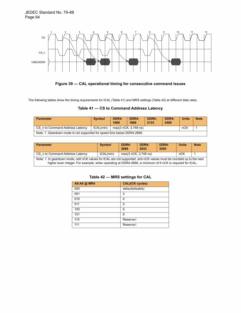
JEDEC Standard No. 79-4BPage 64
Figure 39 — CAL operational timing for consecutive command issues
The following tables show the timing requirements for tCAL (Table 41) and MRS settings (Table 42) at different data rates.
Table 41 — CS to Command Address Latency
Table 42 — MRS settings for CAL
Parameter Symbol DDR4-1600
DDR4-1866
DDR4-2133
DDR4-2400
Units Note
CS_n to Command Address Latency tCAL(min) max(3 nCK, 3.748 ns) nCK 1
Note: 1. Geardown mode is not supported for speed bins below DDR4-2666.
Parameter Symbol DDR4-2666
DDR4-2933
DDR4-3200
Units Note
CS_n to Command Address Latency tCAL(min) max(3 nCK, 3.748 ns) nCK 1
Note: 1. In geardown mode, odd nCK values for tCAL are not supported, and nCK values must be rounded up to the next higher even integer. For example, when operating at DDR4-2666, a minimum of 6 nCK is required for tCAL.
A8:A6 @ MR4 CAL(tCK cycles)
000 default(disable)
001 3
010 4
011 5
100 6
101 8
110 Reserved
111 Reserved
CK
CS_n
CMD/ADDR
1 2 3 4 5 6 7 8 9 10 11 12
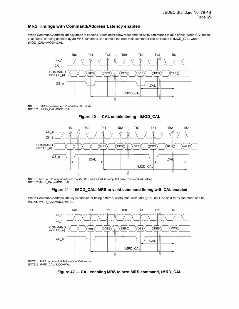
JEDEC Standard No. 79-4B Page 65
MRS Timings with Command/Address Latency enabled
When Command/Address latency mode is enabled, users must allow more time for MRS commands to take effect. When CAL mode is enabled, or being enabled by an MRS command, the earliest the next valid command can be issued is tMOD_CAL, where tMOD_CAL=tMOD+tCAL.
NOTE 1 MRS command at Ta1 enables CAL mode NOTE 2 tMOD_CAL=tMOD+tCAL
Figure 40 — CAL enable timing - tMOD_CAL
NOTE 1 MRS at Ta1 may or may not modify CAL, tMOD_CAL is computed based on new tCAL setting. NOTE 2 tMOD_CAL=tMOD+tCAL.
Figure 41 — tMOD_CAL, MRS to valid command timing with CAL enabled
When Command/Address latency is enabled or being entered, users must wait tMRD_CAL until the next MRS command can be issued. tMRD_CAL=tMOD+tCAL.
NOTE 1 MRS command at Ta1 enables CAL mode NOTE 2 tMRD_CAL=tMOD+tCAL
Figure 42 — CAL enabling MRS to next MRS command, tMRD_CAL
CK_t
COMMAND
CK_c
Ta0 Ta1 Ta2 Tb0 Tb1 Tb2 Tc0
VALIDDESDESDESMRS(w/o CS_n)
CS_ntCAL
tMOD_CAL
DES
CK_t
COMMAND
CK_cT0 Ta0 Ta1 Ta2 Tb0 Tb1 Tb2
DESDESMRS(w/o CS_n)
CS_ntCAL
tMOD_CAL
DES
Tc0
VALIDDES
tCAL
CK_t
COMMAND
CK_c
Ta0 Ta1 Ta2 Tb0 Tb1 Tb2 Tc0
MRSDESDESDESMRS(w/o CS_n)
CS_ntCAL
tMRD_CAL
DES
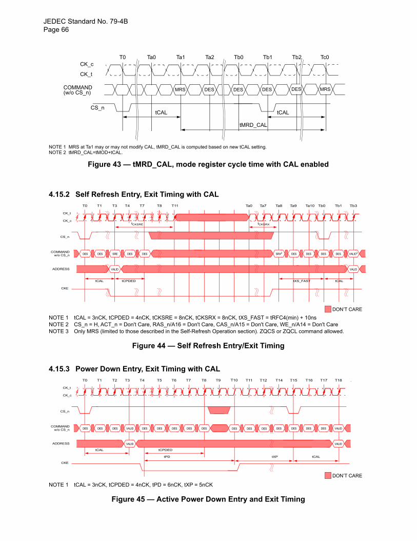
JEDEC Standard No. 79-4BPage 66
NOTE 1 MRS at Ta1 may or may not modify CAL, tMRD_CAL is computed based on new tCAL setting. NOTE 2 tMRD_CAL=tMOD+tCAL.
Figure 43 — tMRD_CAL, mode register cycle time with CAL enabled
4.15.2 Self Refresh Entry, Exit Timing with CAL
CK_t
T8 Ta0 . . Ta10 . Tb1 .Ta8T0 T3
CS_n
COMMAND
tCKSRE
T4 T7 Ta7 Ta9 Tb0 Tb3
DES DES SRE DES DES SRX2 DES DES DES DES VALID3
ADDRESS VALID VALID
DON’T CARE
CK_c
T1 T11
tCKSRX
w/o CS_n
CKE
tCAL tCPDED tXS_FAST tCAL
NOTE 1 tCAL = 3nCK, tCPDED = 4nCK, tCKSRE = 8nCK, tCKSRX = 8nCK, tXS_FAST = tRFC4(min) + 10ns NOTE 2 CS_n = H, ACT_n = Don't Care, RAS_n/A16 = Don't Care, CAS_n/A15 = Don't Care, WE_n/A14 = Don't Care NOTE 3 Only MRS (limited to those described in the Self-Refresh Operation section). ZQCS or ZQCL command allowed.
Figure 44 — Self Refresh Entry/Exit Timing
4.15.3 Power Down Entry, Exit Timing with CAL
CK_t
T5 T11 . . T16 T18 .T14T0 T2
CS_n
COMMAND
T3 T4 T12 T15 T17
DES DES DES VALID DES DES DES DES DES VALID
ADDRESS VALID VALID
DON’T CARE
CK_c
T1 T6
w/o CS_n
CKE
tCAL tCPDED
tXP tCAL
T7 T8 T9 T10
DES DES DESDES DES DES DES
tPD
NOTE 1 tCAL = 3nCK, tCPDED = 4nCK, tPD = 6nCK, tXP = 5nCK
Figure 45 — Active Power Down Entry and Exit Timing
CK_t
COMMAND
CK_cT0 Ta0 Ta1 Ta2 Tb0 Tb1 Tb2
DESDESMRS(w/o CS_n)
CS_ntCAL
tMRD_CAL
DES
Tc0
MRSDES
tCAL
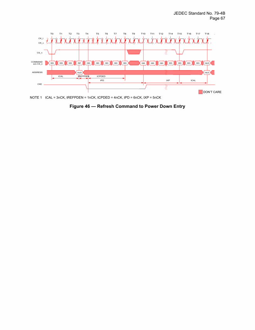
JEDEC Standard No. 79-4B Page 67
NOTE 1 tCAL = 3nCK, tREFPDEN = 1nCK, tCPDED = 4nCK, tPD = 6nCK, tXP = 5nCK
Figure 46 — Refresh Command to Power Down Entry
CK_t
T5 T11 . . T16 T18 .T14T0 T2
CS_n
COMMAND
T3 T4 T12 T15 T17
DES DES DES REF DES DES DES DES DES VALID
ADDRESS VALID VALID
DON’T CARE
CK_c
T1 T6
w/o CS_n
CKE
tCAL tCPDED
tXP tCAL
T7 T8 T9 T10
DES DES DESDES DES DES DES
tPD
tREFPDEN
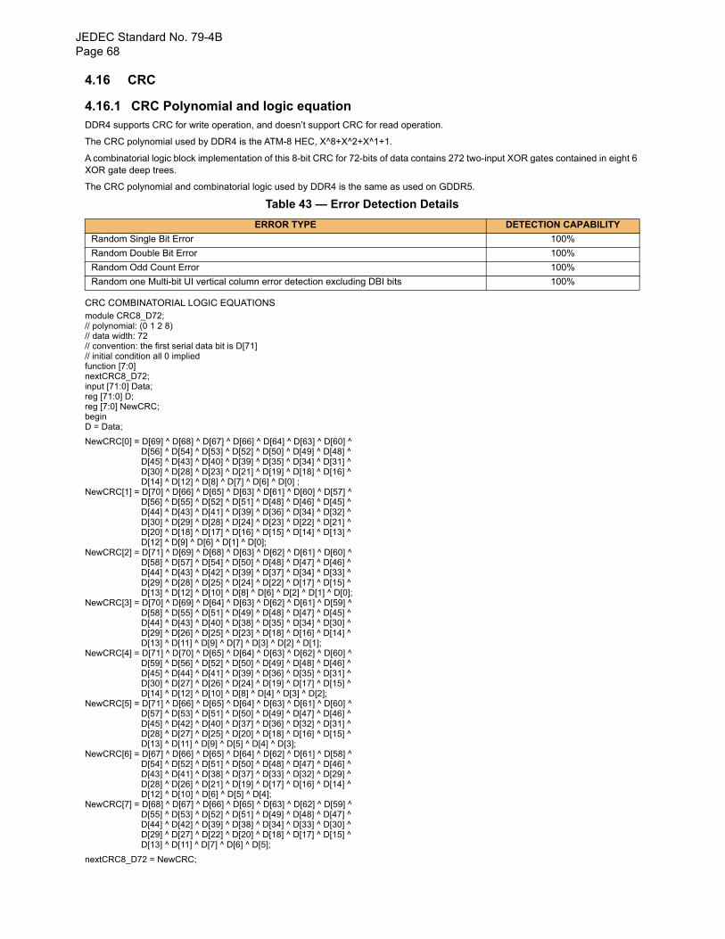
JEDEC Standard No. 79-4BPage 68
4.16 CRC
4.16.1 CRC Polynomial and logic equationDDR4 supports CRC for write operation, and doesn’t support CRC for read operation.
The CRC polynomial used by DDR4 is the ATM-8 HEC, X^8+X^2+X^1+1.
A combinatorial logic block implementation of this 8-bit CRC for 72-bits of data contains 272 two-input XOR gates contained in eight 6 XOR gate deep trees.
The CRC polynomial and combinatorial logic used by DDR4 is the same as used on GDDR5.
Table 43 — Error Detection Details
CRC COMBINATORIAL LOGIC EQUATIONSmodule CRC8_D72;// polynomial: (0 1 2 8)// data width: 72// convention: the first serial data bit is D[71]// initial condition all 0 impliedfunction [7:0]nextCRC8_D72;input [71:0] Data;reg [71:0] D;reg [7:0] NewCRC;beginD = Data;
NewCRC[0] = D[69] ^ D[68] ^ D[67] ^ D[66] ^ D[64] ^ D[63] ^ D[60] ^D[56] ^ D[54] ^ D[53] ^ D[52] ^ D[50] ^ D[49] ^ D[48] ^D[45] ^ D[43] ^ D[40] ^ D[39] ^ D[35] ^ D[34] ^ D[31] ^D[30] ^ D[28] ^ D[23] ^ D[21] ^ D[19] ^ D[18] ^ D[16] ^D[14] ^ D[12] ^ D[8] ^ D[7] ^ D[6] ^ D[0] ;
NewCRC[1] = D[70] ^ D[66] ^ D[65] ^ D[63] ^ D[61] ^ D[60] ^ D[57] ^D[56] ^ D[55] ^ D[52] ^ D[51] ^ D[48] ^ D[46] ^ D[45] ^D[44] ^ D[43] ^ D[41] ^ D[39] ^ D[36] ^ D[34] ^ D[32] ^D[30] ^ D[29] ^ D[28] ^ D[24] ^ D[23] ^ D[22] ^ D[21] ^D[20] ^ D[18] ^ D[17] ^ D[16] ^ D[15] ^ D[14] ^ D[13] ^D[12] ^ D[9] ^ D[6] ^ D[1] ^ D[0];
NewCRC[2] = D[71] ^ D[69] ^ D[68] ^ D[63] ^ D[62] ^ D[61] ^ D[60] ^D[58] ^ D[57] ^ D[54] ^ D[50] ^ D[48] ^ D[47] ^ D[46] ^D[44] ^ D[43] ^ D[42] ^ D[39] ^ D[37] ^ D[34] ^ D[33] ^D[29] ^ D[28] ^ D[25] ^ D[24] ^ D[22] ^ D[17] ^ D[15] ^D[13] ^ D[12] ^ D[10] ^ D[8] ^ D[6] ^ D[2] ^ D[1] ^ D[0];
NewCRC[3] = D[70] ^ D[69] ^ D[64] ^ D[63] ^ D[62] ^ D[61] ^ D[59] ^D[58] ^ D[55] ^ D[51] ^ D[49] ^ D[48] ^ D[47] ^ D[45] ^D[44] ^ D[43] ^ D[40] ^ D[38] ^ D[35] ^ D[34] ^ D[30] ^D[29] ^ D[26] ^ D[25] ^ D[23] ^ D[18] ^ D[16] ^ D[14] ^D[13] ^ D[11] ^ D[9] ^ D[7] ^ D[3] ^ D[2] ^ D[1];
NewCRC[4] = D[71] ^ D[70] ^ D[65] ^ D[64] ^ D[63] ^ D[62] ^ D[60] ^D[59] ^ D[56] ^ D[52] ^ D[50] ^ D[49] ^ D[48] ^ D[46] ^D[45] ^ D[44] ^ D[41] ^ D[39] ^ D[36] ^ D[35] ^ D[31] ^D[30] ^ D[27] ^ D[26] ^ D[24] ^ D[19] ^ D[17] ^ D[15] ^D[14] ^ D[12] ^ D[10] ^ D[8] ^ D[4] ^ D[3] ^ D[2];
NewCRC[5] = D[71] ^ D[66] ^ D[65] ^ D[64] ^ D[63] ^ D[61] ^ D[60] ^D[57] ^ D[53] ^ D[51] ^ D[50] ^ D[49] ^ D[47] ^ D[46] ^D[45] ^ D[42] ^ D[40] ^ D[37] ^ D[36] ^ D[32] ^ D[31] ^D[28] ^ D[27] ^ D[25] ^ D[20] ^ D[18] ^ D[16] ^ D[15] ^D[13] ^ D[11] ^ D[9] ^ D[5] ^ D[4] ^ D[3];
NewCRC[6] = D[67] ^ D[66] ^ D[65] ^ D[64] ^ D[62] ^ D[61] ^ D[58] ^D[54] ^ D[52] ^ D[51] ^ D[50] ^ D[48] ^ D[47] ^ D[46] ^D[43] ^ D[41] ^ D[38] ^ D[37] ^ D[33] ^ D[32] ^ D[29] ^D[28] ^ D[26] ^ D[21] ^ D[19] ^ D[17] ^ D[16] ^ D[14] ^D[12] ^ D[10] ^ D[6] ^ D[5] ^ D[4];
NewCRC[7] = D[68] ^ D[67] ^ D[66] ^ D[65] ^ D[63] ^ D[62] ^ D[59] ^D[55] ^ D[53] ^ D[52] ^ D[51] ^ D[49] ^ D[48] ^ D[47] ^D[44] ^ D[42] ^ D[39] ^ D[38] ^ D[34] ^ D[33] ^ D[30] ^D[29] ^ D[27] ^ D[22] ^ D[20] ^ D[18] ^ D[17] ^ D[15] ^D[13] ^ D[11] ^ D[7] ^ D[6] ^ D[5];
nextCRC8_D72 = NewCRC;
ERROR TYPE DETECTION CAPABILITY
Random Single Bit Error 100%
Random Double Bit Error 100%
Random Odd Count Error 100%
Random one Multi-bit UI vertical column error detection excluding DBI bits 100%
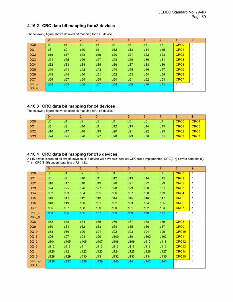
JEDEC Standard No. 79-4B Page 69
4.16.2 CRC data bit mapping for x8 devices
The following figure shows detailed bit mapping for a x8 device.
4.16.3 CRC data bit mapping for x4 devicesThe following figure shows detailed bit mapping for a x4 device.
4.16.4 CRC data bit mapping for x16 devicesA x16 device is treated as two x8 devices. x16 device will have two identical CRC trees implemented. CRC(0-7) covers data bits d(0-71). CRC(8-15) covers data bits d(72-143).
0 1 2 3 4 5 6 7 8 9
DQ0 d0 d1 d2 d3 d4 d5 d6 d7 CRC0 1
DQ1 d8 d9 d10 d11 d12 d13 d14 d15 CRC1 1
DQ2 d16 d17 d18 d19 d20 d21 d22 d23 CRC2 1
DQ3 d24 d25 d26 d27 d28 d29 d30 d31 CRC3 1
DQ4 d32 d33 d34 d35 d36 d37 d38 d39 CRC4 1
DQ5 d40 d41 d42 d43 d44 d45 d46 d47 CRC5 1
DQ6 d48 d49 d50 d51 d52 d53 d54 d55 CRC6 1
DQ7 d56 d57 d58 d59 d60 d61 d62 d63 CRC7 1
DM_n/DBI_n
d64 d65 d66 d67 d68 d69 d70 d71 1 1
0 1 2 3 4 5 6 7 8 9
DQ0 d0 d1 d2 d3 d4 d5 d6 d7 CRC0 CRC4
DQ1 d8 d9 d10 d11 d12 d13 d14 d15 CRC1 CRC5
DQ2 d16 d17 d18 d19 d20 d21 d22 d23 CRC2 CRC6
DQ3 d24 d25 d26 d27 d28 d29 d30 d31 CRC3 CRC7
0 1 2 3 4 5 6 7 8 9
DQ0 d0 d1 d2 d3 d4 d5 d6 d7 CRC0 1
DQ1 d8 d9 d10 d11 d12 d13 d14 d15 CRC1 1
DQ2 d16 d17 d18 d19 d20 d21 d22 d23 CRC2 1
DQ3 d24 d25 d26 d27 d28 d29 d30 d31 CRC3 1
DQ4 d32 d33 d34 d35 d36 d37 d38 d39 CRC4 1
DQ5 d40 d41 d42 d43 d44 d45 d46 d47 CRC5 1
DQ6 d48 d49 d50 d51 d52 d53 d54 d55 CRC6 1
DQ7 d56 d57 d58 d59 d60 d61 d62 d63 CRC7 1
DML_n/DBIL_n
d64 d65 d66 d67 d68 d69 d70 d71 1 1
DQ8 d72 d73 d74 d75 d76 d77 d78 d79 CRC8 1
DQ9 d80 d81 d82 d83 d84 d85 d86 d87 CRC9 1
DQ10 d88 d89 d90 d91 d92 d93 d94 d95 CRC10 1
DQ11 d96 d97 d98 d99 d100 d101 d102 d103 CRC11 1
DQ12 d104 d105 d106 d107 d108 d109 d110 d111 CRC12 1
DQ13 d112 d113 d114 d115 d116 d117 d118 d119 CRC13 1
DQ14 d120 d121 d122 d123 d124 d125 d126 d127 CRC14 1
DQ15 d128 d129 d130 d131 d132 d133 d134 d135 CRC15 1
DMU_n/DBIU_n
d136 d137 d138 d139 d140 d141 d142 d143 1 1
JEDEC Standard No. 79-4BPage 70
4.16.5 Write CRC for x4, x8 and x16 devicesThe Controller generates the CRC checksum and forms the write data frames as shown in Section 4.16.1 to Section 4.16.4.
For a x8 DRAM the controller must send 1’s in the transfer 9 if CRC is enabled and must send 1’s in transfer 8 and transfer 9 of the DBI_n lane if DBI function is enabled.
For a x16 DRAM the controller must send 1’s in the transfer 9 if CRC is enabled and must send 1’s in transfer 8 and transfer 9 of the DBIL_n and DBIU_n lanes if DBI function is enabled.
The DRAM checks for an error in a received code word D[71:0] by comparing the received checksum against the computed checksum and reports errors using the ALERT_n signal if there is a mis-match.
A x8 device has a CRC tree with 72 input bits. The upper 8 bits are used if either Write DBI or DM is enabled. Note that Write DBI and DM function cannot be enabled simultaneously. If both Write DBI and DM is disabled then the inputs of the upper 8 bits D[71:64] are ‘1’s.
A x16 device has two identical CRC trees with 72 input bits each. The upper 8 bits are used if either Write DBI or DM is enabled. Note that Write DBI and DM function cannot be enabled simultaneously. If both Write DBI and DM is disabled then the inputs of the upper 8 bits [D(143:136) and D(71:64)] are ‘1’s.
A x4 device has a CRC tree with 32 input bits. The input for the upper 40 bits D[71:32] are ‘1’s.
DRAM can write data to the DRAM core without waiting for CRC check for full writes. If bad data is written to the DRAM core then controller will retry the transaction and overwrite the bad data. Controller is responsible for data coherency.
4.16.6 CRC Error Handling CRC Error mechanism shares the same Alert_n signal for reporting errors on writes to DRAM. The controller has no way to distinguish between CRC errors and Command/Address/Parity errors other than to read the DRAM mode registers. This is a very time consuming process in a multi-rank configuration.
To speed up recovery for CRC errors, CRC errors are only sent back as a pulse. The minimum pulse-width is six clocks. The latency to Alert_n signal is defined as tCRC_ALERT in the figure below.
DRAM will set CRC Error Clear bit in A3 of MR5 to '1' and CRC Error Status bit in MPR3 of page1 to '1' upon detecting a CRC error. The CRC Error Clear bit remains set at '1' until the host clears it explicitly using an MRS command.
The controller upon seeing an error as a pulse width will retry the write transactions. The controller understands the worst case delay for Alert_n (during init) and can backup the transactions accordingly or the controller can be made more intelligent and try to correlate the write CRC error to a specific rank or a transaction. The controller is also responsible for opening any pages and ensuring that retrying of writes is done in a coherent fashion.
The pulse width may be seen longer than six clocks at the controller if there are multiple CRC errors as the Alert_n is a daisy chain bus.
Figure 47 — CRC Error Reporting
Table 44 — CRC Error Timing Parmeters
DDR4-1600 DDR4-1866 DDR4-2133 DDR4-2400 Unit
Parameter Symbol min max min max min max min max
CRC error to ALERT_n latency tCRC_ALERT - 13 - 13 - 13 - 13 ns
CRC ALERT_n pulse width CRC ALERT_PW 6 10 6 10 6 10 6 10 nCK
CK_cT0 T1 T2 T3 T4 T5 T6 Ta0 Ta1 Ta2
DQ
Alert_n
CRC ALERT_PW(max)
Ta3 Ta4 Ta5
CK_t
CRC ALERT_PW(min)
TIME BREAK
TRANSITIONING DATA
D1 D2 D3 D4 D5 D6 D7 1’SCRCD0
tCRC_ALERT
NOTE 1 CRC ALERT_PW is specified from the point where the DRAM starts to drive the signal low to the point where the DRAM driver releases and the controller starts to pull the signal up.
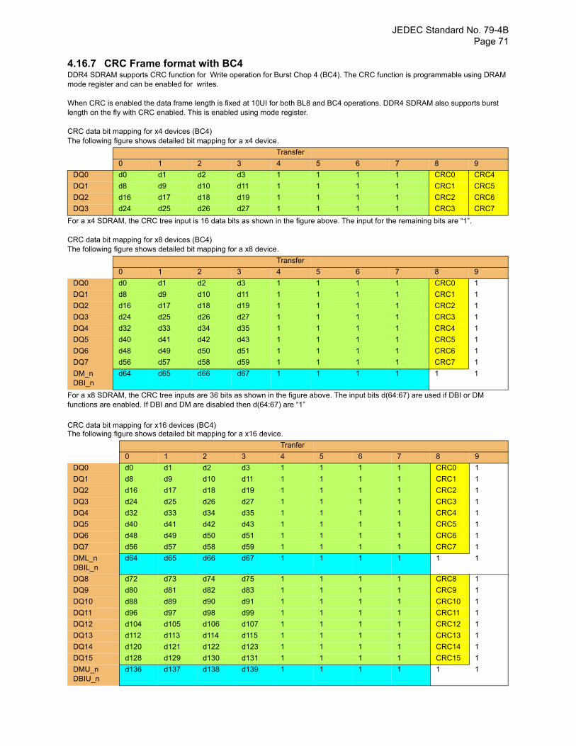
JEDEC Standard No. 79-4B Page 71
4.16.7 CRC Frame format with BC4 DDR4 SDRAM supports CRC function for Write operation for Burst Chop 4 (BC4). The CRC function is programmable using DRAM mode register and can be enabled for writes.
When CRC is enabled the data frame length is fixed at 10UI for both BL8 and BC4 operations. DDR4 SDRAM also supports burst length on the fly with CRC enabled. This is enabled using mode register.
CRC data bit mapping for x4 devices (BC4)The following figure shows detailed bit mapping for a x4 device.
For a x4 SDRAM, the CRC tree input is 16 data bits as shown in the figure above. The input for the remaining bits are “1”.
CRC data bit mapping for x8 devices (BC4)The following figure shows detailed bit mapping for a x8 device.
For a x8 SDRAM, the CRC tree inputs are 36 bits as shown in the figure above. The input bits d(64:67) are used if DBI or DM functions are enabled. If DBI and DM are disabled then d(64:67) are “1”
CRC data bit mapping for x16 devices (BC4) The following figure shows detailed bit mapping for a x16 device.
Transfer
0 1 2 3 4 5 6 7 8 9
DQ0 d0 d1 d2 d3 1 1 1 1 CRC0 CRC4
DQ1 d8 d9 d10 d11 1 1 1 1 CRC1 CRC5
DQ2 d16 d17 d18 d19 1 1 1 1 CRC2 CRC6
DQ3 d24 d25 d26 d27 1 1 1 1 CRC3 CRC7
Transfer
0 1 2 3 4 5 6 7 8 9
DQ0 d0 d1 d2 d3 1 1 1 1 CRC0 1
DQ1 d8 d9 d10 d11 1 1 1 1 CRC1 1
DQ2 d16 d17 d18 d19 1 1 1 1 CRC2 1
DQ3 d24 d25 d26 d27 1 1 1 1 CRC3 1
DQ4 d32 d33 d34 d35 1 1 1 1 CRC4 1
DQ5 d40 d41 d42 d43 1 1 1 1 CRC5 1
DQ6 d48 d49 d50 d51 1 1 1 1 CRC6 1
DQ7 d56 d57 d58 d59 1 1 1 1 CRC7 1
DM_nDBI_n
d64 d65 d66 d67 1 1 1 1 1 1
Tranfer
0 1 2 3 4 5 6 7 8 9
DQ0 d0 d1 d2 d3 1 1 1 1 CRC0 1
DQ1 d8 d9 d10 d11 1 1 1 1 CRC1 1
DQ2 d16 d17 d18 d19 1 1 1 1 CRC2 1
DQ3 d24 d25 d26 d27 1 1 1 1 CRC3 1
DQ4 d32 d33 d34 d35 1 1 1 1 CRC4 1
DQ5 d40 d41 d42 d43 1 1 1 1 CRC5 1
DQ6 d48 d49 d50 d51 1 1 1 1 CRC6 1
DQ7 d56 d57 d58 d59 1 1 1 1 CRC7 1
DML_nDBIL_n
d64 d65 d66 d67 1 1 1 1 1 1
DQ8 d72 d73 d74 d75 1 1 1 1 CRC8 1
DQ9 d80 d81 d82 d83 1 1 1 1 CRC9 1
DQ10 d88 d89 d90 d91 1 1 1 1 CRC10 1
DQ11 d96 d97 d98 d99 1 1 1 1 CRC11 1
DQ12 d104 d105 d106 d107 1 1 1 1 CRC12 1
DQ13 d112 d113 d114 d115 1 1 1 1 CRC13 1
DQ14 d120 d121 d122 d123 1 1 1 1 CRC14 1
DQ15 d128 d129 d130 d131 1 1 1 1 CRC15 1
DMU_nDBIU_n
d136 d137 d138 d139 1 1 1 1 1 1
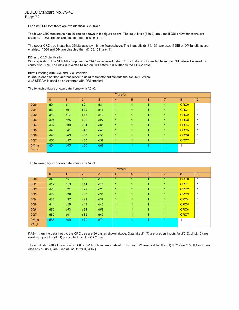
JEDEC Standard No. 79-4BPage 72
For a x16 SDRAM there are two identical CRC trees.
The lower CRC tree inputs has 36 bits as shown in the figure above. The input bits d(64:67) are used if DBI or DM functions are enabled. If DBI and DM are disabled then d(64:67) are “1”.
The upper CRC tree inputs has 36 bits as shown in the figure above. The input bits d(136:139) are used if DBI or DM functions are enabled. If DBI and DM are disabled then d(136:139) are “1”.
DBI and CRC clarificationWrite operation: The SDRAM computes the CRC for received data d(71:0). Data is not inverted based on DBI before it is used for computing CRC. The data is inverted based on DBI before it is written to the DRAM core.
Burst Ordering with BC4 and CRC enabledIf CRC is enabled then address bit A2 is used to transfer critical data first for BC4 writes.A x8 SDRAM is used as an example with DBI enabled.
The following figure shows data frame with A2=0.
The following figure shows data frame with A2=1.
If A2=1 then the data input to the CRC tree are 36 bits as shown above. Data bits d(4:7) are used as inputs for d(0:3), d(12:15) are used as inputs to d(8:11) and so forth for the CRC tree.
The input bits d(68:71) are used if DBI or DM functions are enabled. If DBI and DM are disabled then d(68:71) are “1”s. If A2=1 then data bits d(68:71) are used as inputs for d(64:67)
Transfer
0 1 2 3 4 5 6 7 8 9
DQ0 d0 d1 d2 d3 1 1 1 1 CRC0 1
DQ1 d8 d9 d10 d11 1 1 1 1 CRC1 1
DQ2 d16 d17 d18 d19 1 1 1 1 CRC2 1
DQ3 d24 d25 d26 d27 1 1 1 1 CRC3 1
DQ4 d32 d33 d34 d35 1 1 1 1 CRC4 1
DQ5 d40 d41 d42 d43 1 1 1 1 CRC5 1
DQ6 d48 d49 d50 d51 1 1 1 1 CRC6 1
DQ7 d56 d57 d58 d59 1 1 1 1 CRC7 1
DM_nDBI_n
d64 d65 d66 d67 1 1 1 1 1 1
Transfer
0 1 2 3 4 5 6 7 8 9
DQ0 d4 d5 d6 d7 1 1 1 1 CRC0 1
DQ1 d12 d13 d14 d15 1 1 1 1 CRC1 1
DQ2 d20 d21 d22 d23 1 1 1 1 CRC2 1
DQ3 d28 d29 d30 d31 1 1 1 1 CRC3 1
DQ4 d36 d37 d38 d39 1 1 1 1 CRC4 1
DQ5 d44 d45 d46 d47 1 1 1 1 CRC5 1
DQ6 d52 d53 d54 d55 1 1 1 1 CRC6 1
DQ7 d60 d61 d62 d63 1 1 1 1 CRC7 1
DM_nDBI_n
d68 d69 d70 d71 1 1 1 1 1 1
JEDEC Standard No. 79-4B Page 73
The CRC tree will treat the 36 bits in transfer’s four through seven as 1’s
CRC equations for x8 device in BC4 mode with A2=0 are as follows:
CRC[0] = D[69]=1 ^ D[68]=1 ^ D[67] ^ D[66] ^ D[64] ^ D[63]=1 ^ D[60]=1 ^ D[56] ^ D[54]=1 ^ D[53]=1 ^ D[52]=1 ^ D[50] ^ D[49] ^ D[48] ^ D[45]=1 ^ D[43] ^ D[40] ^ D[39]=1 ^ D[35] ^ D[34] ^ D[31]=1^ D[30]=1 ^ D[28]=1 ^ D[23]=1 ^ D[21]=1 ^ D[19] ^ D[18] ^ D[16] ^ D[14]=1 ^ D[12]=1 ^ D[8] ^ D[7]=1 ^ D[6] =1 ^ D[0] ;
CRC[1] = D[70]=1 ^ D[66] ^ D[65] ^ D[63]=1 ^ D[61]=1 ^ D[60]=1 ^ D[57] ^D[56] ^ D[55]=1 ^ D[52]=1 ^ D[51] ^ D[48] ^ D[46]=1 ^ D[45]=1 ^ D[44]=1 ^ D[43] ^ D[41] ^ D[39]=1 ^ D[36]=1 ^ D[34] ^ D[32] ^ D[30]=1 ^ D[29]=1 ^ D[28]=1 ^ D[24] ^ D[23]=1 ^ D[22]=1 ^ D[21]=1 ^ D[20]=1 ^ D[18] ^ D[17] ^ D[16] ^ D[15]=1 ^ D[14]=1 ^ D[13]=1 ^ D[12]=1 ^ D[9] ^ D[6]=1 ^ D[1] ^ D[0];
CRC[2] = D[71]=1 ^ D[69]=1 ^ D[68]=1 ^ D[63]=1 ^ D[62]=1 ^ D[61]=1 ^ D[60]=1 ^ D[58] ^ D[57] ^ D[54]=1 ^ D[50] ^ D[48] ^ D[47]=1 ^ D[46]=1 ^ D[44]=1 ^ D[43] ^ D[42] ^ D[39]=1 ^ D[37]=1 ^ D[34] ^ D[33] ^
D[29]=1 ^ D[28]=1 ^ D[25] ^ D[24] ^ D[22]=1 ^ D[17] ^ D[15]=1 ^ D[13]=1 ^ D[12]=1 ^ D[10] ^ D[8] ^ D[6]=1 ^ D[2] ^ D[1] ^ D[0];
CRC[3] = D[70]=1 ^ D[69]=1 ^ D[64] ^ D[63]=1 ^ D[62]=1 ^ D[61]=1 ^ D[59] ^ D[58] ^ D[55]=1 ^ D[51] ^ D[49] ^ D[48] ^ D[47]=1 ^ D[45]=1 ^ D[44]=1 ^ D[43] ^ D[40] ^ D[38]=1 ^ D[35] ^ D[34] ^ D[30]=1 ^ D[29]=1 ^ D[26] ^ D[25] ^ D[23]=1 ^ D[18] ^ D[16] ^ D[14]=1 ^ D[13]=1 ^ D[11] ^ D[9] ^ D[7]=1 ^ D[3] ^ D[2] ^ D[1];
CRC[4] = D[71]=1 ^ D[70]=1 ^ D[65] ^ D[64] ^ D[63]=1 ^ D[62]=1 ^ D[60]=1 ^ D[59] ^ D[56] ^ D[52]=1 ^ D[50] ^ D[49] ^ D[48] ^ D[46]=1 ^ D[45]=1 ^ D[44]=1 ^ D[41] ^ D[39]=1 ^ D[36]=1 ^ D[35] ^ D[31]=1 ^
D[30]=1 ^ D[27] ^ D[26] ^ D[24] ^ D[19] ^ D[17] ^ D[15]=1 ^ D[14]=1 ^ D[12]=1 ^ D[10] ^ D[8] ^ D[4]=1 ^ D[3] ^ D[2];CRC[5] = D[71]=1 ^ D[66] ^ D[65] ^ D[64] ^ D[63]=1 ^ D[61]=1 ^ D[60]=1 ^ D[57] ^ D[53]=1 ^ D[51] ^ D[50] ^ D[49] ^ D[47]=1 ^
D[46]=1 ^ D[45]=1 ^ D[42] ^ D[40] ^ D[37]=1 ^ D[36]=1 ^ D[32] ^ D[31]=1 ^ D[28]=1 ^ D[27] ^ D[25] ^ D[20]=1 ^ D[18] ^ D[16] ^ D[15]=1 ^ D[13]=1 ^ D[11] ^ D[9] ^ D[5]=1 ^ D[4]=1 ^ D[3];
CRC[6] = D[67] ^ D[66] ^ D[65] ^ D[64] ^ D[62]=1 ^ D[61]=1 ^ D[58] ^ D[54]=1 ^ D[52]=1 ^ D[51] ^ D[50] ^ D[48] ^ D[47]=1 ^ D[46]=1 ^ D[43] ^ D[41] ^ D[38]=1 ^ D[37]=1 ^ D[33] ^ D[32] ^ D[29]=1 ^ D[28]=1 ^ D[26] ^ D[21]=1 ^ D[19] ^ D[17] ^ D[16] ^ D[14]=1 ^ D[12]=1 ^ D[10] ^ D[6]=1 ^ D[5]=1 ^ D[4]=1;
CRC[7] = D[68]=1 ^ D[67] ^ D[66] ^ D[65] ^ D[63]=1 ^ D[62]=1 ^ D[59] ^ D[55]=1 ^ D[53]=1 ^ D[52]=1 ^ D[51] ^ D[49] ^ D[48] ^ D[47]=1 ^ D[44]=1 ^ D[42] ^ D[39]=1 ^ D[38]=1 ^ D[34] ^ D[33] ^ D[30]=1 ^ D[29]=1 ^ D[27] ^ D[22]=1 ^ D[20]=1 ^ D[18] ^ D[17] ^ D[15] =1^ D[13]=1 ^ D[11] ^ D[7]=1 ^ D[6]=1 ^ D[5]=1;
CRC equations for x8 device in BC4 mode with A2=1 are as follows:
CRC[0] = 1 ^ 1 ^ D[71] ^ D[70] ^ D[68] ^ 1 ^ 1 ^ D[60] ^ 1 ^ 1 ^ 1 ^ D[54] ^ D[53] ^ D[52] ^ 1 ^ D[47] ^ D[44] ^ 1 ^ D[39] ^ D[38] ^ 1^ 1 ^ 1 ^ 1 ^ 1 ^ D[23] ^ D[22] ^ D[20] ^ 1 ^ 1 ^ D[12] ^ 1 ^ 1 ^ D[4] ;
CRC[1] = 1 ^ D[70] ^ D[69] ^ 1 ^ 1 ^ 1 ^ D[61] ^ D[60] ^ 1 ^ 1 ^ D[55] ^ D[52] ^ 1 ^ 1 ^ 1 ^ D[47] ^ D[45] ^ 1 ^ 1 ^ D[38] ^ D[36] ^ 1 ^ 1 ^ 1 ^ D[28] ^ 1 ^ 1 ^ 1 ^ 1 ^ D[22] ^ D[21] ^ D[20] ^1 ^ 1 ^1 ^ 1 ^ D[13] ^ 1 ^ D[5] ^ D[4];
CRC[2] = 1 ^ 1 ^ 1 ^1 ^1 ^ 1 ^ 1 ^ D[62] ^ D[61] ^ 1 ^ D[54] ^ D[52] ^ 1 ^ 1 ^ 1 ^ D[47] ^ D[46] ^ 1 ^ 1 ^ D[38] ^ D[37] ^ 1 ^ 1 ^ D[29] ^ D[28] ^ 1 ^ D[21] ^ 1 ^ 1 ^ 1 ^ D[14] ^ D12] ^1 ^ D[6] ^ D[5] ^ D[4];
CRC[3] = 1 ^ 1 ^ D[68] ^ 1 ^ 1 ^ 1 ^ D[63] ^ D[62] ^ 1 ^ D[55] ^ D[53] ^ D[52] ^ 1 ^ 1 ^ 1 ^ D[47] ^ D[44] ^ 1 ^ D[39] ^ D[38] ^ 1 ^ 1 ^ D[30] ^ D[29] ^ 1 ^ D[22] ^ D[20] ^ 1 ^ 1 ^ D[15] ^ D[13] ^ 1 ^ D[7] ^ D[6] ^ D[5];
CRC[4] = 1 ^1 ^ D[69] ^ D[68] ^ 1 ^ 1 ^ 1 ^ D[63] ^ D[60] ^ 1 ^ D[54] ^ D[53] ^ D[52] ^ 1 ^1 ^ 1 ^ D[45] ^ 1 ^ 1 ^ D[39] ^1 ^ 1 ^ D[31] ^ D[30] ^ D[28] ^ D[23] ^ D[21] ^ 1 ^ 1 ^ 1 ^ D[14] ^ D[12] ^ 1 ^ D[7] ^ D[6];
CRC[5] = 1 ^ D[70] ^ D[69] ^ D[68] ^ 1 ^ 1 ^ 1 ^ D[61] ^ 1 ^ D[55] ^ D[54] ^ D[53] ^ 1 ^ 1 ^ 1 ^ D[46] ^ D[44] ^ 1 ^ 1 ^ D[36] ^ 1 ^ 1 ^ D[31] ^ D[29] ^ 1 ^ D[22] ^ D[20] ^ 1 ^ 1 ^ D[15] ^ D[13] ^ 1 ^ 1 ^ D[7];
CRC[6] = D[71] ^ D[70] ^ D[69] ^ D[68] ^ 1 ^ 1 ^ D[62] ^ 1 ^ 1 ^ D[55] ^ D[54] ^ D[52] ^ 1 ^1 ^ D[47] ^ D[45] ^ 1 ^ 1 ^ D[37] ^ D[36] ^1 ^ 1 ^ D[30] ^ 1 ^ D[23] ^ D[21] ^ D[20] ^ 1 ^ 1 ^ D[14] ^ 1 ^ 1 ^ 1;
CRC[7] = 1 ^ D[71] ^ D[70] ^ D[69] ^ 1 ^ 1 ^ D[63] ^ 1 ^ 1 ^ 1 ^ D[55] ^ D[53] ^ D[52] ^ 1 ^ 1 ^ D[46] ^ 1 ^ 1 ^ D[38] ^ D[37] ^ 1 ^ 1 ^ D[31] ^ 1 ^ 1 ^ D[22] ^ D[21] ^ 1^ 1 ^ D[15] ^ 1 ^ 1 ^ 1;
4.16.8 Simultaneous DM and CRC Functionality
When both DM and Write CRC are enabled in the DRAM mode register, the DRAM calculates CRC before sending the write data into the array. If there is a CRC error, the DRAM blocks the write operation and discards the data. For a x16, when the DRAM detects an error in CRC tree, DDR4 DRAMs may mask all DQs or half the DQs depending upon the specific vendor implementation behavior. Both implementations are valid. For the DDR4 DRAMs that masking half the DQs, DQ0 through DQ7 will be masked if the lower byte CRC tree had the error and DQ8 through DQ15 will be masked if the upper byte CRC tree had the error.
4.16.9 Simultaneous MPR Write, Per DRAM Addressability and CRC Functionality
The following combination of DDR4 features are prohibited for simultaneous operation
1) MPR Write and Write CRC (Note: MPR Write is via Address pins) 2) Per DRAM Addressability and Write CRC (Note : Only MRS are allowed during PDA and also DQ0 is used for PDA detection)
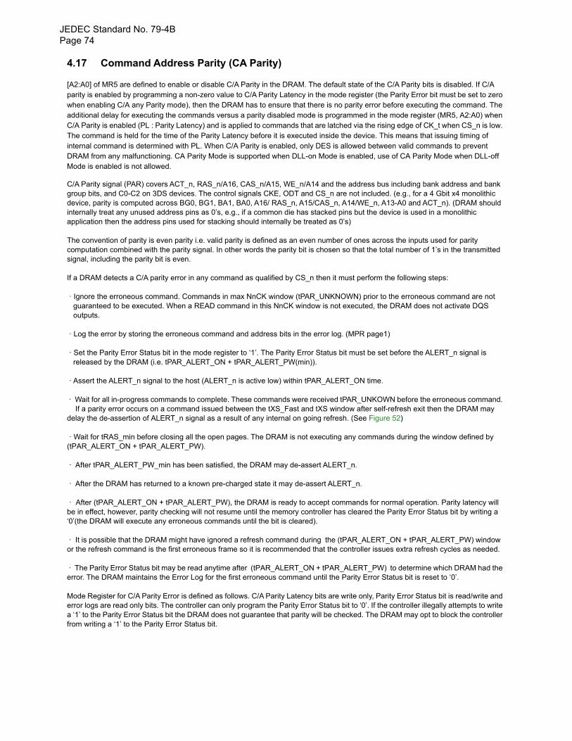
JEDEC Standard No. 79-4BPage 74
4.17 Command Address Parity (CA Parity)
[A2:A0] of MR5 are defined to enable or disable C/A Parity in the DRAM. The default state of the C/A Parity bits is disabled. If C/A parity is enabled by programming a non-zero value to C/A Parity Latency in the mode register (the Parity Error bit must be set to zero when enabling C/A any Parity mode), then the DRAM has to ensure that there is no parity error before executing the command. The additional delay for executing the commands versus a parity disabled mode is programmed in the mode register (MR5, A2:A0) when C/A Parity is enabled (PL : Parity Latency) and is applied to commands that are latched via the rising edge of CK_t when CS_n is low. The command is held for the time of the Parity Latency before it is executed inside the device. This means that issuing timing of internal command is determined with PL. When C/A Parity is enabled, only DES is allowed between valid commands to prevent DRAM from any malfunctioning. CA Parity Mode is supported when DLL-on Mode is enabled, use of CA Parity Mode when DLL-off Mode is enabled is not allowed.
C/A Parity signal (PAR) covers ACT_n, RAS_n/A16, CAS_n/A15, WE_n/A14 and the address bus including bank address and bank group bits, and C0-C2 on 3DS devices. The control signals CKE, ODT and CS_n are not included. (e.g., for a 4 Gbit x4 monolithic device, parity is computed across BG0, BG1, BA1, BA0, A16/ RAS_n, A15/CAS_n, A14/WE_n, A13-A0 and ACT_n). (DRAM should internally treat any unused address pins as 0’s, e.g., if a common die has stacked pins but the device is used in a monolithic application then the address pins used for stacking should internally be treated as 0’s)
The convention of parity is even parity i.e. valid parity is defined as an even number of ones across the inputs used for paritycomputation combined with the parity signal. In other words the parity bit is chosen so that the total number of 1’s in the transmittedsignal, including the parity bit is even.
If a DRAM detects a C/A parity error in any command as qualified by CS_n then it must perform the following steps:
· Ignore the erroneous command. Commands in max NnCK window (tPAR_UNKNOWN) prior to the erroneous command are not guaranteed to be executed. When a READ command in this NnCK window is not executed, the DRAM does not activate DQS outputs. · Log the error by storing the erroneous command and address bits in the error log. (MPR page1) · Set the Parity Error Status bit in the mode register to ‘1’. The Parity Error Status bit must be set before the ALERT_n signal is released by the DRAM (i.e. tPAR_ALERT_ON + tPAR_ALERT_PW(min)). · Assert the ALERT_n signal to the host (ALERT_n is active low) within tPAR_ALERT_ON time. · Wait for all in-progress commands to complete. These commands were received tPAR_UNKOWN before the erroneous command. If a parity error occurs on a command issued between the tXS_Fast and tXS window after self-refresh exit then the DRAM may delay the de-assertion of ALERT_n signal as a result of any internal on going refresh. (See Figure 52)
· Wait for tRAS_min before closing all the open pages. The DRAM is not executing any commands during the window defined by (tPAR_ALERT_ON + tPAR_ALERT_PW).
· After tPAR_ALERT_PW_min has been satisfied, the DRAM may de-assert ALERT_n.
· After the DRAM has returned to a known pre-charged state it may de-assert ALERT_n.
· After (tPAR_ALERT_ON + tPAR_ALERT_PW), the DRAM is ready to accept commands for normal operation. Parity latency will be in effect, however, parity checking will not resume until the memory controller has cleared the Parity Error Status bit by writing a ‘0’(the DRAM will execute any erroneous commands until the bit is cleared).
· It is possible that the DRAM might have ignored a refresh command during the (tPAR_ALERT_ON + tPAR_ALERT_PW) window or the refresh command is the first erroneous frame so it is recommended that the controller issues extra refresh cycles as needed.
· The Parity Error Status bit may be read anytime after (tPAR_ALERT_ON + tPAR_ALERT_PW) to determine which DRAM had the error. The DRAM maintains the Error Log for the first erroneous command until the Parity Error Status bit is reset to ‘0’.
Mode Register for C/A Parity Error is defined as follows. C/A Parity Latency bits are write only, Parity Error Status bit is read/write and error logs are read only bits. The controller can only program the Parity Error Status bit to ‘0’. If the controller illegally attempts to write a ‘1’ to the Parity Error Status bit the DRAM does not guarantee that parity will be checked. The DRAM may opt to block the controller from writing a ‘1’ to the Parity Error Status bit.
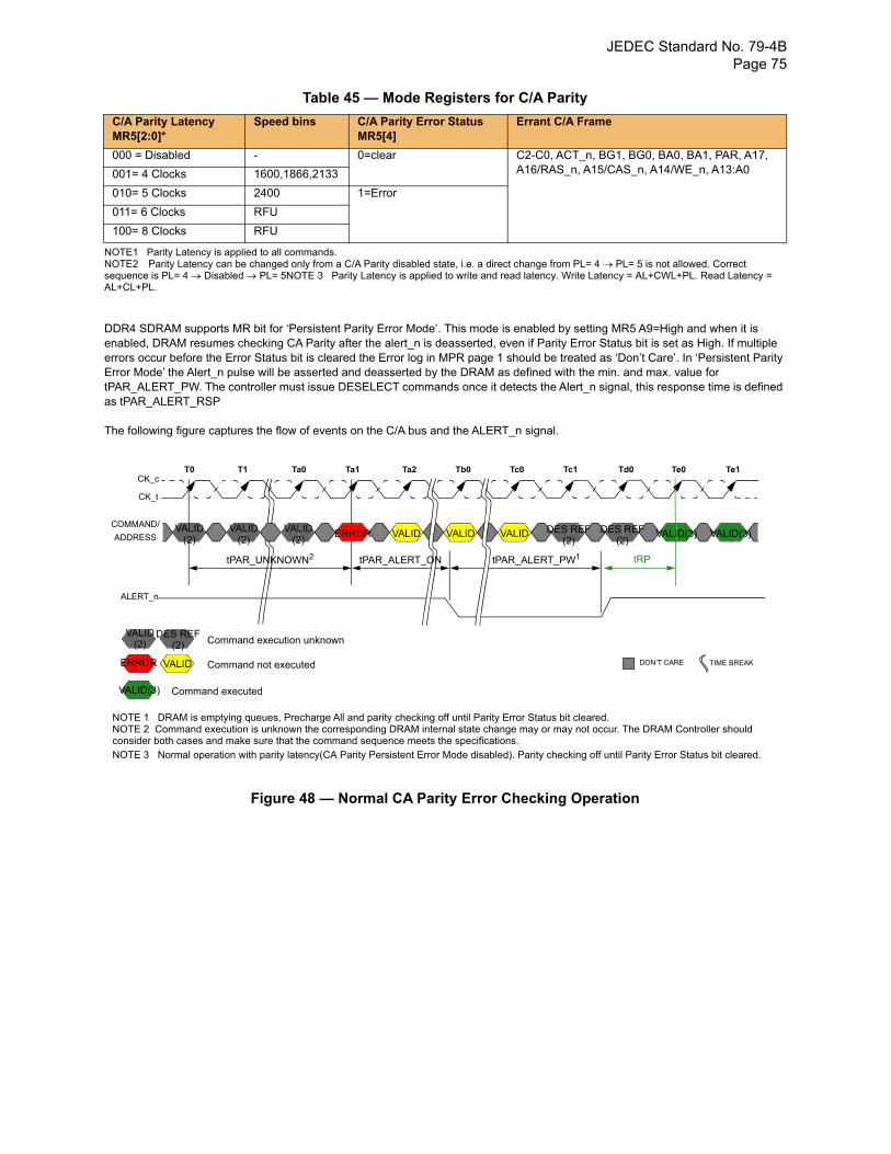
JEDEC Standard No. 79-4B Page 75
Table 45 — Mode Registers for C/A Parity
NOTE1 Parity Latency is applied to all commands. NOTE2 Parity Latency can be changed only from a C/A Parity disabled state, i.e. a direct change from PL= 4 PL= 5 is not allowed. Correct sequence is PL= 4 Disabled PL= 5NOTE 3 Parity Latency is applied to write and read latency. Write Latency = AL+CWL+PL. Read Latency = AL+CL+PL.
DDR4 SDRAM supports MR bit for ‘Persistent Parity Error Mode’. This mode is enabled by setting MR5 A9=High and when it is enabled, DRAM resumes checking CA Parity after the alert_n is deasserted, even if Parity Error Status bit is set as High. If multiple errors occur before the Error Status bit is cleared the Error log in MPR page 1 should be treated as ‘Don’t Care’. In ‘Persistent Parity Error Mode’ the Alert_n pulse will be asserted and deasserted by the DRAM as defined with the min. and max. value for tPAR_ALERT_PW. The controller must issue DESELECT commands once it detects the Alert_n signal, this response time is defined as tPAR_ALERT_RSP
The following figure captures the flow of events on the C/A bus and the ALERT_n signal.
Figure 48 — Normal CA Parity Error Checking Operation
C/A Parity Latency MR5[2:0]*
Speed bins C/A Parity Error Status MR5[4]
Errant C/A Frame
000 = Disabled - 0=clear C2-C0, ACT_n, BG1, BG0, BA0, BA1, PAR, A17, A16/RAS_n, A15/CAS_n, A14/WE_n, A13:A0001= 4 Clocks 1600,1866,2133
010= 5 Clocks 2400 1=Error
011= 6 Clocks RFU
100= 8 Clocks RFU
T1 Ta0 Ta1CK_c
CK_t
T0 Tb0 Tc0 Tc1Ta2 Te0 Te1Td0
COMMAND/
ADDRESS
ALERT_n
VALID(3) VALID(3)ERROR VALID VALID VALIDVALID VALID VALID
Command execution unknown
Command not executed
Command executed
tPAR_ALERT_ON tPAR_ALERT_PW1
TIME BREAKDON’T CARE
DES REF DES REF
tPAR_UNKNOWN2
NOTE 1 DRAM is emptying queues, Precharge All and parity checking off until Parity Error Status bit cleared.NOTE 2 Command execution is unknown the corresponding DRAM internal state change may or may not occur. The DRAM Controller should consider both cases and make sure that the command sequence meets the specifications.NOTE 3 Normal operation with parity latency(CA Parity Persistent Error Mode disabled). Parity checking off until Parity Error Status bit cleared.
(2)(2)(2) (2) (2)
VALID(2)
DES REF(2)
ERROR VALID
VALID(3)
tRP
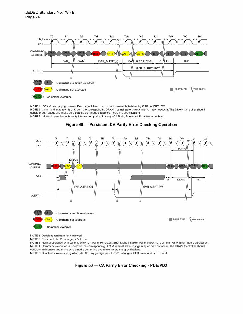
JEDEC Standard No. 79-4BPage 76
Figure 49 — Persistent CA Parity Error Checking Operation
Figure 50 — CA Parity Error Checking - PDE/PDX
T1 Ta0 Ta1CK_c
CK_t
T0 Tb0 Tc0 Tc1Ta2 Te0 Te1Td0
COMMAND/
ADDRESS
ALERT_n
VALID(3)ERROR VALID VALID VALIDVALID VALID VALID
Command execution unknown
Command not executed
Command executed
tPAR_ALERT_ON
TIME BREAKDON’T CARE
DES
tPAR_UNKNOWN2
NOTE 1 DRAM is emptying queues, Precharge All and parity check re-enable finished by tPAR_ALERT_PW.NOTE 2 Command execution is unknown the corresponding DRAM internal state change may or may not occur. The DRAM Controller should consider both cases and make sure that the command sequence meets the specifications.NOTE 3 Normal operation with parity latency and parity checking (CA Parity Persistent Error Mode enabled).
(2) (2) (2)
VALID(2)
DES
ERROR VALID
VALID(3)
DES DES
tPAR_ALERT_PW1
tRPtPAR_ALERT_RSP t 2nCK
CK_c
CK_t
T1 Ta0 Ta1T0 Tb1 Tc0 Tc1Tb0 Td1 Td2Td0 Td3 Te0 Te1
tXP+PL
tCPDED
tPAR_ALERT_ON tPAR_ALERT_PW1
COMMAND/
ADDRESS
ALERT_n
CKE
ERROR(2) DES(1) DES(1) VALID(3)
Command execution unknown
Command not executed
Command executed
TIME BREAKDON’T CARE
NOTE 1 Deselect command only allowed.NOTE 2 Error could be Precharge or Activate. NOTE 3 Normal operation with parity latency (CA Parity Persistent Error Mode disable). Parity checking is off until Parity Error Status bit cleared.NOTE 4 Command execution is unknown the corresponding DRAM internal state change may or may not occur. The DRAM Controller should consider both cases and make sure that the command sequence meets the specifications.NOTE 5 Deselect command only allowed CKE may go high prior to Td2 as long as DES commands are issued.
tIS tRPt 2nCK
tIS
tIH
DES REF(4)
DES(5)
ERROR(2) DES(1)
VALID(3)
DES(5) DES(5) DES REF(4)
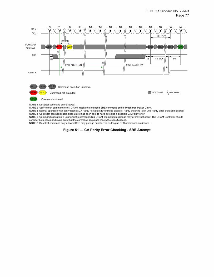
JEDEC Standard No. 79-4B Page 77
Figure 51 — CA Parity Error Checking - SRE Attempt
CK_c
CK_t
T1 Ta0 Ta1T0 Tb1 Td0 Td1Tb0 Td1 Td2Td0 Td3 Te0 Te1
tXP+PL
tCPDED
tPAR_ALERT_ON tPAR_ALERT_PW1
COMMAND/
ADDRESS
ALERT_n
CKE
DES(1) VALID(3)
Command execution unknown
Command not executed
Command executed
TIME BREAKDON’T CARE
NOTE 1 Deselect command only allowed.NOTE 2 SelfRefresh command error. DRAM masks the intended SRE command enters Precharge Power Down. NOTE 3 Normal operation with parity latency(CA Parity Persistent Error Mode disable). Parity checking is off until Parity Error Status bit cleared.NOTE 4 Controller can not disable clock until it has been able to have detected a possible C/A Parity error.NOTE 5 Command execution is unknown the corresponding DRAM internal state change may or may not occur. The DRAM Controller should consider both cases and make sure that the command sequence meets the specifications.NOTE 6 Deselect command only allowed CKE may go high prior to Tc2 as long as DES commands are issued.
tIS tRPt 2nCK
tIS
tIH
DES (1,5) DES(6)
ERROR(2) DES(1)
VALID(3)
ERROR(2)DES(1,5) DES(6) DES(6) DES(5)
(4)
DES REF(5)
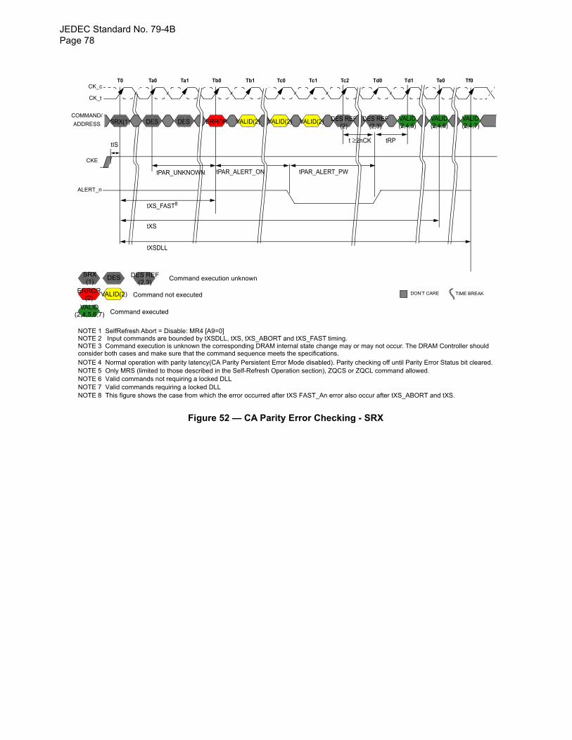
JEDEC Standard No. 79-4BPage 78
Figure 52 — CA Parity Error Checking - SRX
Ta0 Ta1 Tb0CK_c
CK_t
T0 Td1 Te0Td0
COMMAND/
ADDRESS
ALERT_n
VALID VALIDERROR VALID(2) VALID(2) VALID(2)SRX(1) DES
Command execution unknown
Command not executed
Command executed
tPAR_ALERT_ON tPAR_ALERT_PW
TIME BREAKDON’T CARE
DES REF DES REF
tPAR_UNKNOWN
NOTE 1 SelfRefresh Abort = Disable: MR4 [A9=0]NOTE 2 Input commands are bounded by tXSDLL, tXS, tXS_ABORT and tXS_FAST timing. NOTE 3 Command execution is unknown the corresponding DRAM internal state change may or may not occur. The DRAM Controller should consider both cases and make sure that the command sequence meets the specifications.NOTE 4 Normal operation with parity latency(CA Parity Persistent Error Mode disabled). Parity checking off until Parity Error Status bit cleared.NOTE 5 Only MRS (limited to those described in the Self-Refresh Operation section), ZQCS or ZQCL command allowed.NOTE 6 Valid commands not requiring a locked DLLNOTE 7 Valid commands requiring a locked DLLNOTE 8 This figure shows the case from which the error occurred after tXS FAST_An error also occur after tXS_ABORT and tXS.
(2,3)(2)
SRX(1)
DES
ERRORVALID(2)
VALID
Tf0
VALIDDES(2,4,5) (2,4,6) (2,4,7)
CKE
Tc0 Tc1 Tc2Tb1
tXS_FAST8
tXS
tXSDLL
tIStRPt 2nCK
DES REF(2,3)
(2)
(2,4,5,6,7)
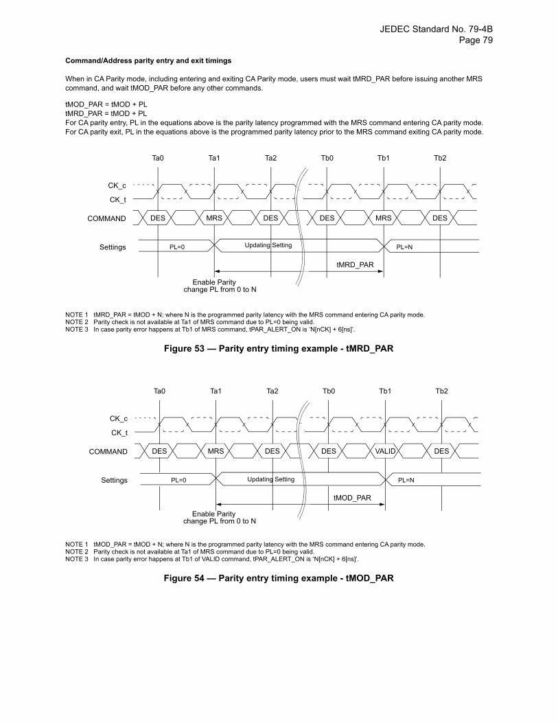
JEDEC Standard No. 79-4B Page 79
Command/Address parity entry and exit timings
When in CA Parity mode, including entering and exiting CA Parity mode, users must wait tMRD_PAR before issuing another MRS command, and wait tMOD_PAR before any other commands.
tMOD_PAR = tMOD + PLtMRD_PAR = tMOD + PLFor CA parity entry, PL in the equations above is the parity latency programmed with the MRS command entering CA parity mode. For CA parity exit, PL in the equations above is the programmed parity latency prior to the MRS command exiting CA parity mode.
NOTE 1 tMRD_PAR = tMOD + N; where N is the programmed parity latency with the MRS command entering CA parity mode.NOTE 2 Parity check is not available at Ta1 of MRS command due to PL=0 being valid.NOTE 3 In case parity error happens at Tb1 of MRS command, tPAR_ALERT_ON is ‘N[nCK] + 6[ns]’.
Figure 53 — Parity entry timing example - tMRD_PAR
NOTE 1 tMOD_PAR = tMOD + N; where N is the programmed parity latency with the MRS command entering CA parity mode.NOTE 2 Parity check is not available at Ta1 of MRS command due to PL=0 being valid.NOTE 3 In case parity error happens at Tb1 of VALID command, tPAR_ALERT_ON is ‘N[nCK] + 6[ns]’.
Figure 54 — Parity entry timing example - tMOD_PAR
CK_t
COMMAND
CK_c
Ta0 Ta1 Ta2 Tb0 Tb1 Tb2
Settings
tMRD_PAR
DES
Enable Parity
PL=0 Updating Setting PL=N
MRS DES DES MRS DES
change PL from 0 to N
CK_t
COMMAND
CK_c
Ta0 Ta1 Ta2 Tb0 Tb1 Tb2
Settings
tMOD_PAR
DES
PL=0 Updating Setting PL=N
MRS DES DES VALID DES
Enable Paritychange PL from 0 to N
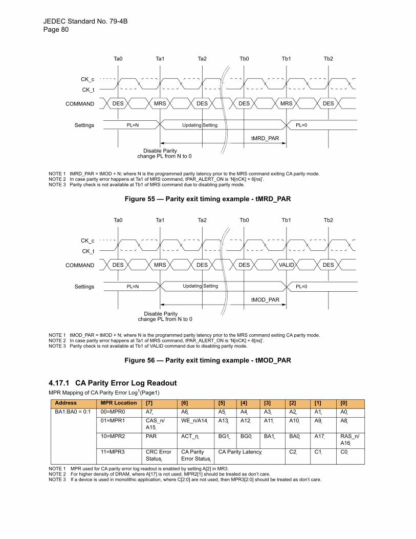
JEDEC Standard No. 79-4BPage 80
CK_t
COMMAND
CK_c
Ta0 Ta1 Ta2 Tb0 Tb1 Tb2
Settings
tMRD_PAR
DES
PL=N Updating Setting PL=0
MRS DES DES MRS DES
Disable Paritychange PL from N to 0
NOTE 1 tMRD_PAR = tMOD + N; where N is the programmed parity latency prior to the MRS command exiting CA parity mode.NOTE 2 In case parity error happens at Ta1 of MRS command, tPAR_ALERT_ON is ‘N[nCK] + 6[ns]’.NOTE 3 Parity check is not available at Tb1 of MRS command due to disabling parity mode.
Figure 55 — Parity exit timing example - tMRD_PAR
CK_t
COMMAND
CK_c
Ta0 Ta1 Ta2 Tb0 Tb1 Tb2
Settings
tMOD_PAR
DES
PL=N PL=0
MRS DES DES VALID DES
Updating Setting
Disable Paritychange PL from N to 0
NOTE 1 tMOD_PAR = tMOD + N; where N is the programmed parity latency prior to the MRS command exiting CA parity mode.NOTE 2 In case parity error happens at Ta1 of MRS command, tPAR_ALERT_ON is ‘N[nCK] + 6[ns]’.NOTE 3 Parity check is not available at Tb1 of VALID command due to disabling parity mode.
Figure 56 — Parity exit timing example - tMOD_PAR
4.17.1 CA Parity Error Log Readout MPR Mapping of CA Parity Error Log1(Page1)
NOTE 1 MPR used for CA parity error log readout is enabled by setting A[2] in MR3.NOTE 2 For higher density of DRAM, where A[17] is not used, MPR2[1] should be treated as don’t care.NOTE 3 If a device is used in monolithic application, where C[2:0] are not used, then MPR3[2:0] should be treated as don’t care.
Address MPR Location [7] [6] [5] [4] [3] [2] [1] [0]
BA1:BA0 = 0:1 00=MPR0 A7 A6 A5 A4 A3 A2 A1 A0
01=MPR1 CAS_n/A15
WE_n/A14 A13 A12 A11 A10 A9 A8
10=MPR2 PAR ACT_n BG1 BG0 BA1 BA0 A17 RAS_n/A16
11=MPR3 CRC Error Status
CA Parity Error Status
CA Parity Latency C2 C1 C0
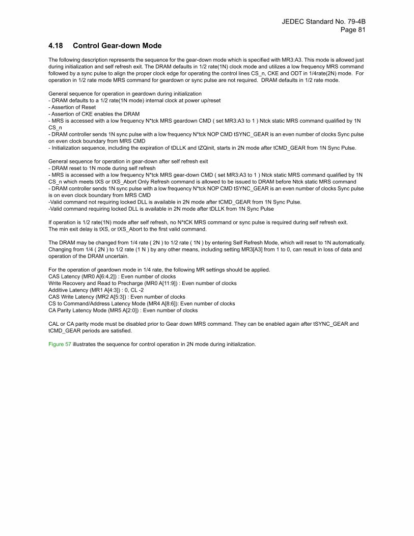
JEDEC Standard No. 79-4B Page 81
4.18 Control Gear-down Mode
The following description represents the sequence for the gear-down mode which is specified with MR3:A3. This mode is allowed just during initialization and self refresh exit. The DRAM defaults in 1/2 rate(1N) clock mode and utilizes a low frequency MRS command followed by a sync pulse to align the proper clock edge for operating the control lines CS_n, CKE and ODT in 1/4rate(2N) mode. For operation in 1/2 rate mode MRS command for geardown or sync pulse are not required. DRAM defaults in 1/2 rate mode.
General sequence for operation in geardown during initialization- DRAM defaults to a 1/2 rate(1N mode) internal clock at power up/reset- Assertion of Reset- Assertion of CKE enables the DRAM- MRS is accessed with a low frequency N*tck MRS geardown CMD ( set MR3:A3 to 1 ) Ntck static MRS command qualified by 1N CS_n- DRAM controller sends 1N sync pulse with a low frequency N*tck NOP CMD tSYNC_GEAR is an even number of clocks Sync pulse on even clock boundary from MRS CMD- Initialization sequence, including the expiration of tDLLK and tZQinit, starts in 2N mode after tCMD_GEAR from 1N Sync Pulse.
General sequence for operation in gear-down after self refresh exit- DRAM reset to 1N mode during self refresh- MRS is accessed with a low frequency N*tck MRS gear-down CMD ( set MR3:A3 to 1 ) Ntck static MRS command qualified by 1N CS_n which meets tXS or tXS_Abort Only Refresh command is allowed to be issued to DRAM before Ntck static MRS command- DRAM controller sends 1N sync pulse with a low frequency N*tck NOP CMD tSYNC_GEAR is an even number of clocks Sync pulse is on even clock boundary from MRS CMD-Valid command not requiring locked DLL is available in 2N mode after tCMD_GEAR from 1N Sync Pulse.-Valid command requiring locked DLL is available in 2N mode after tDLLK from 1N Sync Pulse
If operation is 1/2 rate(1N) mode after self refresh, no N*tCK MRS command or sync pulse is required during self refresh exit.The min exit delay is tXS, or tXS_Abort to the first valid command.
The DRAM may be changed from 1/4 rate ( 2N ) to 1/2 rate ( 1N ) by entering Self Refresh Mode, which will reset to 1N automatically.Changing from 1/4 ( 2N ) to 1/2 rate (1 N ) by any other means, including setting MR3[A3] from 1 to 0, can result in loss of data andoperation of the DRAM uncertain.
For the operation of geardown mode in 1/4 rate, the following MR settings should be applied.CAS Latency (MR0 A[6:4,2]) : Even number of clocksWrite Recovery and Read to Precharge (MR0 A[11:9]) : Even number of clocksAdditive Latency (MR1 A[4:3]) : 0, CL -2CAS Write Latency (MR2 A[5:3]) : Even number of clocksCS to Command/Address Latency Mode (MR4 A[8:6]): Even number of clocksCA Parity Latency Mode (MR5 A[2:0]) : Even number of clocks
CAL or CA parity mode must be disabled prior to Gear down MRS command. They can be enabled again after tSYNC_GEAR and tCMD_GEAR periods are satisfied.
Figure 57 illustrates the sequence for control operation in 2N mode during initialization.
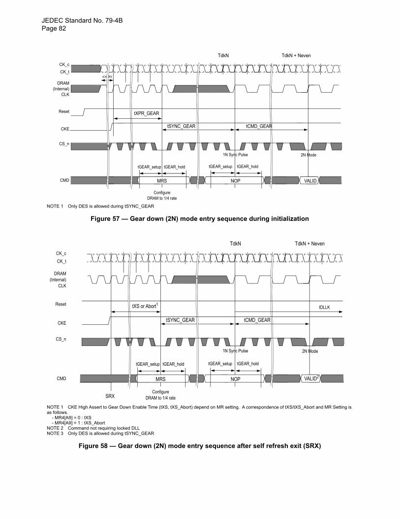
JEDEC Standard No. 79-4BPage 82
NOTE 1 Only DES is allowed during tSYNC_GEAR
Figure 57 — Gear down (2N) mode entry sequence during initialization
NOTE 1 CKE High Assert to Gear Down Enable Time (tXS, tXS_Abort) depend on MR setting. A correspondence of tXS/tXS_Abort and MR Setting is as follows. - MR4[A9] = 0 : tXS - MR4[A9] = 1 : tXS_AbortNOTE 2 Command not requiring locked DLLNOTE 3 Only DES is allowed during tSYNC_GEAR
Figure 58 — Gear down (2N) mode entry sequence after self refresh exit (SRX)
CK_c
DRAM
CK_t
Reset
CKE
CS_n
CMD
(Internal)CLK
tXPR_GEAR
tCMD_GEAR
1N Sync Pulse 2N Mode
MRS NOP VALID
ConfigureDRAM to 1/4 rate
tGEAR_setup
TdkN TdkN + Neven
tGEAR_setup tGEAR_holdtGEAR_hold
tSYNC_GEAR
tCKSRX
CK_c
DRAM
CK_t
Reset
CKE
CS_n
CMD
(Internal)CLK
tXS or Abort1
tCMD_GEAR
1N Sync Pulse 2N Mode
MRS NOP VALID2
ConfigureDRAM to 1/4 rate
tGEAR_setup
TdkN TdkN + Neven
tGEAR_setup tGEAR_holdtGEAR_hold
tSYNC_GEAR
SRX
tDLLK
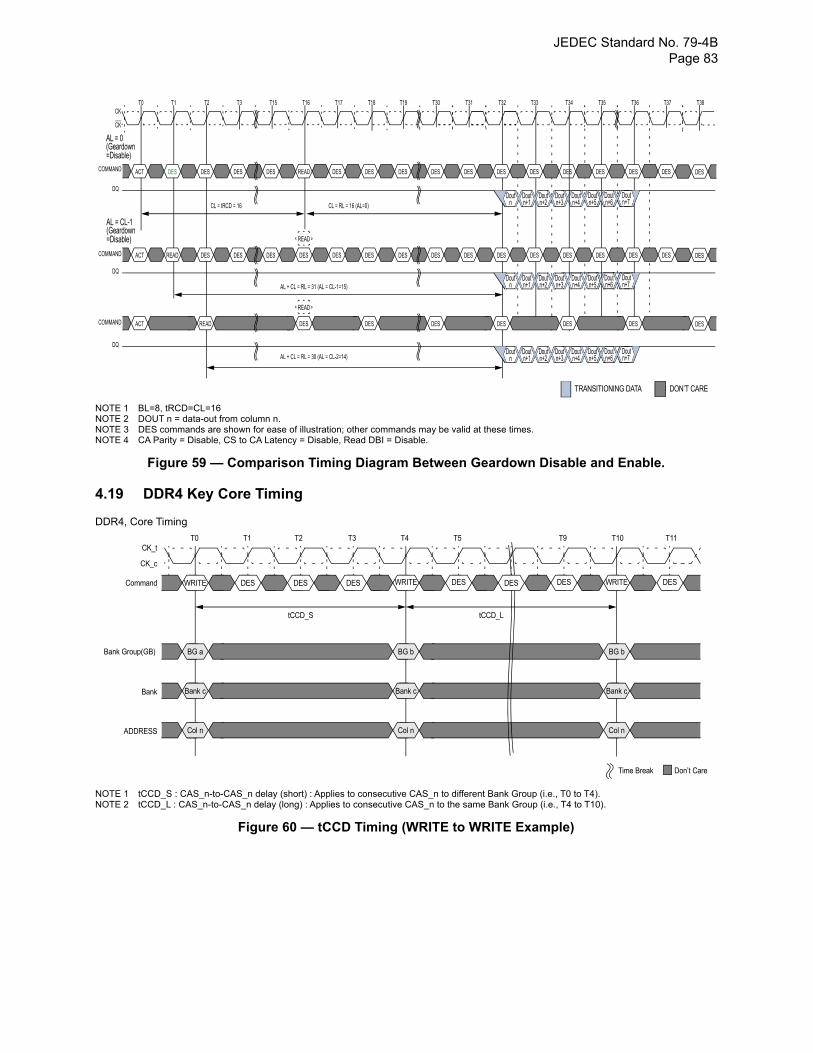
JEDEC Standard No. 79-4B Page 83
NOTE 1 BL=8, tRCD=CL=16NOTE 2 DOUT n = data-out from column n.NOTE 3 DES commands are shown for ease of illustration; other commands may be valid at these times.NOTE 4 CA Parity = Disable, CS to CA Latency = Disable, Read DBI = Disable.
Figure 59 — Comparison Timing Diagram Between Geardown Disable and Enable.
4.19 DDR4 Key Core Timing
DDR4, Core Timing
NOTE 1 tCCD_S : CAS_n-to-CAS_n delay (short) : Applies to consecutive CAS_n to different Bank Group (i.e., T0 to T4).NOTE 2 tCCD_L : CAS_n-to-CAS_n delay (long) : Applies to consecutive CAS_n to the same Bank Group (i.e., T4 to T10).
Figure 60 — tCCD Timing (WRITE to WRITE Example)
DES
CK
CK
T0 T1 T3 T15 T16 T17T2 T18 T19 T30 T31 T32 T33
DON’T CARETRANSITIONING DATA
T34 T35 T37 T38T36
COMMAND
AL = 0 (Geardown=Disable)
ACT DES DES DES DES DESREAD DES DES DES DES DES DES DES DES DES DES DES
DQ Dout
nDoutn+2
Doutn+3
Doutn+1
Doutn+4
Doutn+7
Doutn+5
Doutn+6CL = RL = 16 (AL=0)CL = tRCD = 16
COMMAND ACT READ DES DES DES DESDES DES DES DES DES DES DES DES DES DES DES DES
AL = CL-1(Geardown=Disable) READ
DQ Dout
nDoutn+2
Doutn+3
Doutn+1
Doutn+4
Doutn+7
Doutn+5
Doutn+6AL + CL = RL = 31 (AL = CL-1=15)
COMMAND ACT READ DESDES DES DES DES DES
READ
DQ Dout
nDoutn+2
Doutn+3
Doutn+1
Doutn+4
Doutn+7
Doutn+5
Doutn+6AL + CL = RL = 30 (AL = CL-2=14)
CK_t
CK_c
T0 T1 T2 T3 T4 T5 T9 T10
WRITE DES DES DES WRITE DES DES WRITECommand
BG a BG b BG bBank Group(GB)
Time Break Don’t Care
T11
DES
Bank c Bank c Bank c
Col n Col n Col n
Bank
ADDRESS
tCCD_S tCCD_L
DES
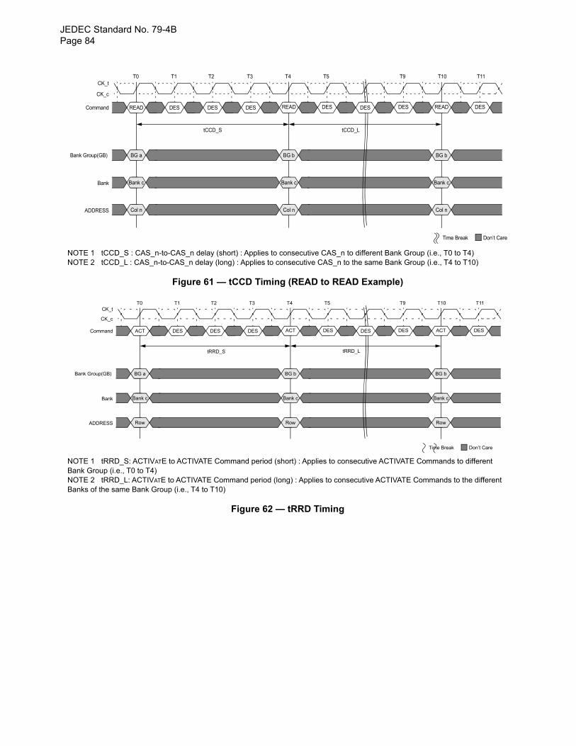
JEDEC Standard No. 79-4BPage 84
NOTE 1 tCCD_S : CAS_n-to-CAS_n delay (short) : Applies to consecutive CAS_n to different Bank Group (i.e., T0 to T4)NOTE 2 tCCD_L : CAS_n-to-CAS_n delay (long) : Applies to consecutive CAS_n to the same Bank Group (i.e., T4 to T10)
Figure 61 — tCCD Timing (READ to READ Example)
NOTE 1 tRRD_S: ACTIVATE to ACTIVATE Command period (short) : Applies to consecutive ACTIVATE Commands to different Bank Group (i.e., T0 to T4)NOTE 2 tRRD_L: ACTIVATE to ACTIVATE Command period (long) : Applies to consecutive ACTIVATE Commands to the different Banks of the same Bank Group (i.e., T4 to T10)
Figure 62 — tRRD Timing
CK_t
CK_c
T0 T1 T2 T3 T4 T5 T9 T10
READ DES DES DES READ DES DES READCommand
BG a BG b BG bBank Group(GB)
Time Break Don’t Care
T11
DES
Bank c Bank c Bank c
Col n Col n Col n
Bank
ADDRESS
tCCD_S tCCD_L
DES
CK_t
CK_c
T0 T1 T2 T3 T4 T5 T9 T10
ACT DES DES DES ACT DES DES ACTCommand
BG a BG b BG bBank Group(GB)
Time Break Don’t Care
T11
DES
Bank c Bank c Bank c
Row Row Row
Bank
ADDRESS
tRRD_L
DES
tRRD_S
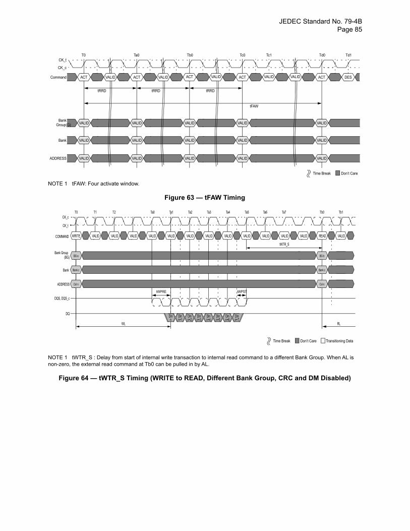
JEDEC Standard No. 79-4B Page 85
NOTE 1 tFAW: Four activate window.
Figure 63 — tFAW Timing
NOTE 1 tWTR_S : Delay from start of internal write transaction to internal read command to a different Bank Group. When AL is non-zero, the external read command at Tb0 can be pulled in by AL.
Figure 64 — tWTR_S Timing (WRITE to READ, Different Bank Group, CRC and DM Disabled)
CK_t
CK_c
T0 Ta0 Tb0 Tc0 Tc1 Td0 Td1
ACT ACT ACT ACT VALID ACT DESCommand
VALID VALID VALID VALID VALIDBank
Time Break Don’t Care
VALID VALID VALID VALID VALIDBank
VALID VALID VALID VALID VALIDADDRESS
Group(G)
tRRD tRRD tRRD
VALID VALID VALID VALID
tFAW
n+2
T2 Ta1 Ta2 Ta3 Ta4Ta0 Ta5 Ta6 Ta7 Tb0 Tb1
WL
Dinn
Dinn+1
Din Dinn+3
Dinn+4
Dinn+5
Dinn+6
Dinn+7
T1T0CK_c
CK_t
COMMAND
Bank Group
DQS, DQS_c
(BG)
DQ
VALID VALID VALID VALID VALID VALID VALID VALID VALID VALID VALID VALID READ VALID
tWTR_S
BG b
Bank cBank Bank c
Col nADDRESS Col n
BG a
tWPSTtWPRE
RL
Time Break Don’t Care Transitioning Data
WRITE
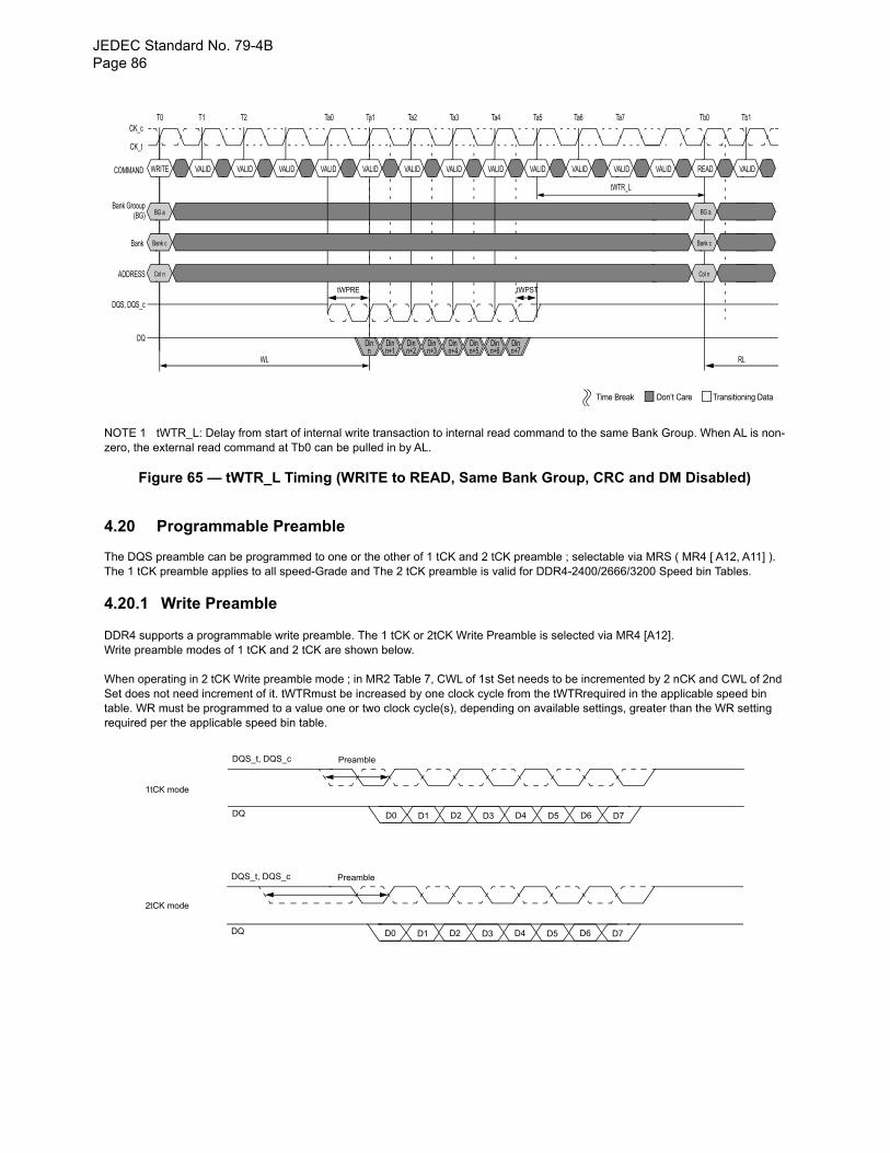
JEDEC Standard No. 79-4BPage 86
NOTE 1 tWTR_L: Delay from start of internal write transaction to internal read command to the same Bank Group. When AL is non-zero, the external read command at Tb0 can be pulled in by AL.
Figure 65 — tWTR_L Timing (WRITE to READ, Same Bank Group, CRC and DM Disabled)
4.20 Programmable Preamble
The DQS preamble can be programmed to one or the other of 1 tCK and 2 tCK preamble ; selectable via MRS ( MR4 [ A12, A11] ). The 1 tCK preamble applies to all speed-Grade and The 2 tCK preamble is valid for DDR4-2400/2666/3200 Speed bin Tables.
4.20.1 Write Preamble
DDR4 supports a programmable write preamble. The 1 tCK or 2tCK Write Preamble is selected via MR4 [A12]. Write preamble modes of 1 tCK and 2 tCK are shown below.
When operating in 2 tCK Write preamble mode ; in MR2 Table 7, CWL of 1st Set needs to be incremented by 2 nCK and CWL of 2nd Set does not need increment of it. tWTRmust be increased by one clock cycle from the tWTRrequired in the applicable speed bin table. WR must be programmed to a value one or two clock cycle(s), depending on available settings, greater than the WR setting required per the applicable speed bin table.
n+2
T2 Ta1 Ta2 Ta3 Ta4Ta0 Ta5 Ta6 Ta7 Tb0 Tb1
WL
Dinn
Dinn+1
Din Dinn+3
Dinn+4
Dinn+5
Dinn+6
Dinn+7
T1T0CK_c
CK_t
COMMAND
Bank Grooup
DQS, DQS_c
(BG)
DQ
VALID VALID VALID VALID VALID VALID VALID VALID VALID VALID VALID VALID READ VALID
tWTR_L
Bank cBank Bank c
Col nADDRESS Col n
BG a
tWPSTtWPRE
RL
Time Break Don’t Care Transitioning Data
WRITE
BG a
1tCK mode
D0 D2 D4 D6D1 D3 D5 D7
2tCK mode
DQS_t, DQS_c
DQ
Preamble
D0 D2 D4 D6D1 D3 D5 D7
DQS_t, DQS_c
DQ
Preamble
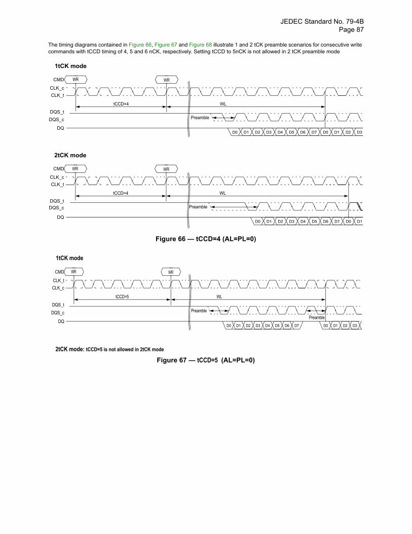
JEDEC Standard No. 79-4B Page 87
The timing diagrams contained in Figure 66, Figure 67 and Figure 68 illustrate 1 and 2 tCK preamble scenarios for consecutive write commands with tCCD timing of 4, 5 and 6 nCK, respectively. Setting tCCD to 5nCK is not allowed in 2 tCK preamble mode
Figure 66 — tCCD=4 (AL=PL=0)
Figure 67 — tCCD=5 (AL=PL=0)
WR
D0D7D6D5D4D3D2D1D0 D1 D2 D3
WR
tCCD=4 WL
PreambleDQS_t
DQS_c
CMD
CLK_c
CLK_t
DQ
1tCK mode
WR
D0D7D6D5D4D3D2D1D0 D1
WR
tCCD=4 WL
Preamble
2tCK mode
DQS_t
CMD
CLK_c
CLK_t
DQ
DQS_c
WR
D7D6D5D4D3D2D1D0 D1 D2 D3
WR
tCCD=5 WL
PreambleDQS_t
DQS_c
CMD
CLK_t
CLK_c
DQ
1tCK mode
2tCK mode: tCCD=5 is not allowed in 2tCK mode
D0
Preamble
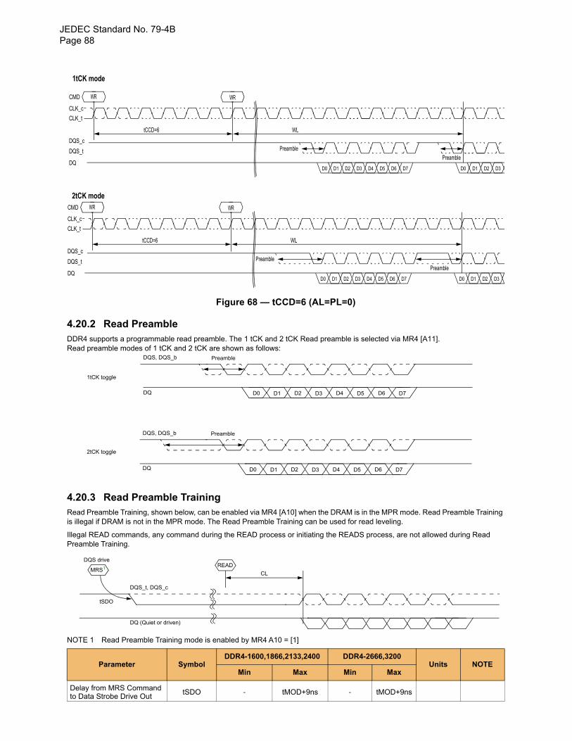
JEDEC Standard No. 79-4BPage 88
Figure 68 — tCCD=6 (AL=PL=0)
4.20.2 Read Preamble DDR4 supports a programmable read preamble. The 1 tCK and 2 tCK Read preamble is selected via MR4 [A11]. Read preamble modes of 1 tCK and 2 tCK are shown as follows:
4.20.3 Read Preamble Training Read Preamble Training, shown below, can be enabled via MR4 [A10] when the DRAM is in the MPR mode. Read Preamble Training is illegal if DRAM is not in the MPR mode. The Read Preamble Training can be used for read leveling.
Illegal READ commands, any command during the READ process or initiating the READS process, are not allowed during Read Preamble Training.
NOTE 1 Read Preamble Training mode is enabled by MR4 A10 = [1]
Parameter SymbolDDR4-1600,1866,2133,2400 DDR4-2666,3200
Units NOTEMin Max Min Max
Delay from MRS Command to Data Strobe Drive Out
tSDO - tMOD+9ns - tMOD+9ns
WR
D7D6D5D4D3D2D1D0 D1 D2 D3
WR
tCCD=6 WL
PreambleDQS_c
DQS_t
CMD
CLK_c
CLK_t
DQ
1tCK mode
D0
Preamble
2tCK modeWR
D7D6D5D4D3D2D1D0 D1 D2 D3
WR
tCCD=6 WL
PreambleDQS_c
DQS_t
CMD
CLK_c
CLK_t
DQD0
Preamble
1tCK toggle
D0 D2 D4 D6D1 D3 D5 D7
2tCK toggle
DQS, DQS_b
DQ
Preamble
D0 D2 D4 D6D1 D3 D5 D7
DQS, DQS_b
DQ
Preamble
DQS_t, DQS_c
DQ (Quiet or driven)
READ
CL
tSDO
MRS1
DQS drive
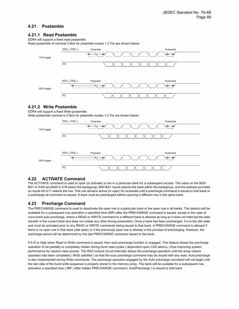
JEDEC Standard No. 79-4B Page 89
4.21 Postamble
4.21.1 Read PostambleDDR4 will support a fixed read postamble.Read postamble of nominal 0.5tck for preamble modes 1,2 Tck are shown below:
4.21.2 Write Postamble DDR4 will support a fixed Write postamble.Write postamble nominal is 0.5tck for preamble modes 1,2 Tck are shown below:
4.22 ACTIVATE CommandThe ACTIVATE command is used to open (or activate) a row in a particular bank for a subsequent access. The value on the BG0-BG1 in X4/8 and BG0 in X16 select the bankgroup; BA0-BA1 inputs selects the bank within the bankgroup, and the address provided on inputs A0-A17 selects the row. This row remains active (or open) for accesses until a precharge command is issued to that bank or a precharge all command is issued. A bank must be precharged before opening a different row in the same bank.
4.23 Precharge Command The PRECHARGE command is used to deactivate the open row in a particular bank or the open row in all banks. The bank(s) will be available for a subsequent row activation a specified time (tRP) after the PRECHARGE command is issued, except in the case of concurrent auto precharge, where a READ or WRITE command to a different bank is allowed as long as it does not interrupt the data transfer in the current bank and does not violate any other timing parameters. Once a bank has been precharged, it is in the idle state and must be activated prior to any READ or WRITE commands being issued to that bank. A PRECHARGE command is allowed if there is no open row in that bank (idle state) or if the previously open row is already in the process of precharging. However, the precharge period will be determined by the last PRECHARGE command issued to the bank.
If A10 is High when Read or Write command is issued, then auto-precharge function is engaged. This feature allows the precharge operation to be partially or completely hidden during burst read cycles ( dependent upon CAS latency ) thus improving system performance for random data access. The RAS lockout circuit internally delays the precharge operation until the array restore operation has been completed ( tRAS satisfied ) so that the auto precharge command may be issued with any read. Auto-precharge is also implemented during Write commands. The precharge operation engaged by the Auto precharge command will not begin until the last data of the burst write sequence is properly stored in the memory array. The bank will be avaiable for a subsequent row activation a specified time ( tRP ) after hidden PRECHARGE command ( AutoPrecharge ) is issued to that bank.
1tCK toggle
2tCK toggle
DQS_t, DQS_c
DQ
Preamble
DQS_t, DQS_c
DQ
Preamble
Postamble
Postamble
1tCK toggle
2tCK toggle
DQS_t, DQS_c
DQ
Preamble
DQS_t, DQS_c
DQ
Preamble
Postamble
Postamble
JEDEC Standard No. 79-4BPage 90
4.24 Read Operation
4.24.1 READ Timing DefinitionsRead timing shown in this section is applied when the DLL is enabled and locked.
Rising data strobe edge parameters: tDQSCK min/max describes the allowed range for a rising data strobe edge relative to CK_t, CK_c. tDQSCK is the actual position of a rising strobe edge relative to CK_t, CK_c. tQSH describes the DQS_t, DQS_c differential output high time. tDQSQ describes the latest valid transition of the associated DQ pins. tQH describes the earliest invalid transition of the associated DQ pins.
Falling data strobe edge parameters: tQSL describes the DQS_t, DQS_c differential output low time. tDQSQ describes the latest valid transition of the associated DQ pins. tQH describes the earliest invalid transition of the associated DQ pins.
tDQSQ; both rising/falling edges of DQS, no tAC defined.
JEDEC Standard No. 79-4B Page 91
Figure 69 — READ Timing Definition
CK_t
CK_c
Rising StrobeVariance
tDQSCK,MIN tDQSCK,MAX
tDQSCK
AssociatedDQ Pins
tDQSCK,MIN tDQSCK,MAX
tDQSCKi
tDQSCK max
DQS_t
DQS_c
tQSH(DQS_t)
tQH tQH
tDQSQ tDQSQ
tDQSCK
Windown
Rising StrobeVariance
tDQSCKi
Windown
Rising StrobeVariance
tDQSCKi
Windown
Rising StrobeVariance
tDQSCKi
Windown
Rising StrobeVariance
tDQSCKi
Windown
Rising StrobeVariance
tDQSCKi
Windown
tDQSCK center
tDQSCK min
tQSL(DQS_t)
JEDEC Standard No. 79-4BPage 92
4.24.1.1 READ Timing; Clock to Data Strobe relationshipClock to Data Strobe relationship is shown in Figure 70 and is applied when the DLL is enabled and locked.
Rising data strobe edge parameters:
tDQSCK min/max describes the allowed range for a rising data strobe edge relative to CK_t, CK_c.
tDQSCK is the actual position of a rising strobe edge relative to CK_t, CK_c.
tQSH describes the data strobe high pulse width.
Falling data strobe edge parameters: - tQSL describes the data strobe low pulse width. - tLZ(DQS), tHZ(DQS) for preamble/postamble.
NOTE 1 Within a burst, rising strobe edge can be varied within tDQSCKi while at the same voltage and temperature. However incorporate the device, voltage and temperature variation, rising strobe edge variance window, tDQSCKi can shift between tDQSCK(min) and tDQSCK(max). A timing of this window’s right inside edge ( latest ) from rising CK_t, CK_c is limited by a device’s actual tDQSCK(max). A timing of this window’s left inside edge (earliest) from rising CK_t, CK_c is limited by tDQSCK(min).
NOTE 2 Notwithstanding note 1, a rising strobe edge with tDQSCK(max) at T(n) can not be immediately followed by a rising strobe edge with tDQSCK(min) at T(n+1). This is because other timing relationships (tQSH, tQSL) exist: if tDQSCK(n+1) < 0: tDQSCK(n) < 1.0 tCK - (tQSHmin + tQSLmin) - |tDQSCK(n+1)|
NOTE 3 The DQS_t, DQS_c differential output high time is defined by tQSH and the DQS_t, DQS_c differential output low time is defined by tQSL.
NOTE 4 Likewise, tLZ(DQS)min and tHZ(DQS)min are not tied to tDQSCKmin (early strobe case) and tLZ(DQS)max and tHZ(DQS)max are not tied to tDQSCKmax (late strobe case).
NOTE 5 The minimum pulse width of read preamble is defined by tRPRE(min).
NOTE 6 The maximum read postamble is bound by tDQSCK(min) plus tQSH(min) on the left side and tHZDQS(max) on the right side.
NOTE 7 The minimum pulse width of read postamble is defined by tRPST(min).
NOTE 8 The maximum read preamble is bound by tLZDQS(min) on the left side and tDQSCK(max) on the right side.
Figure 70 — Clock to Data Strobe Relationship
CK , CK_c
tLZ(DQS)min
tRPRE
DQS_t, DQS_cEarly Strobe
tDQSCK (min)
tQSH
tDQSCK (min) tDQSCK (min) tDQSCK (min)tHZ(DQS)min
tRPST
tLZ(DQS)max
tRPRE
Late Strobe
tDQSCK (max) tDQSCK (max) tDQSCK (max) tDQSCK (max)
tHZ(DQS)max
tRPST
Bit 0 Bit 1 Bit 2 Bit 3 Bit 4 Bit 5 Bit 6 Bit 7
Bit 0 Bit 1 Bit 2 Bit 3 Bit 4 Bit 5 Bit 6 Bit 7
RL measuredto this point
tQSL tQSH tQSL tQSH tQSL
tQSH tQSL tQSH tQSL tQSH tQSL
DQS_t, DQS_c
JEDEC Standard No. 79-4B Page 93
4.24.1.2 READ Timing; Data Strobe to Data relationshipThe Data Strobe to Data relationship is shown in Figure 71 and is applied when the DLL is enabled and locked.
Rising data strobe edge parameters:
tDQSQ describes the latest valid transition of the associated DQ pins.
tQH describes the earliest invalid transition of the associated DQ pins.
Falling data strobe edge parameters:
tDQSQ describes the latest valid transition of the associated DQ pins.
tQH describes the earliest invalid transition of the associated DQ pins.
tDQSQ; both rising/falling edges of DQS, no tAC defined.
Data Valid Window:
tDVWd is the Data Valid Window per device per UI and is derived from (tQH - tDQSQ) of each UI on a given DRAM. This parameter will be characterized and guaranteed by design.
tDVWp is Data Valid Window per pin per UI and is derived from (tQH - tDQSQ) of each UI on a pin of a given DRAM. This parameter will be characterized and guaranteed by design.
NOTE 1 BL = 8, AL = 0, CL = 11, Preamble = 1tCKNOTE 2 DOUT n = data-out from column n.NOTE 3 DES commands are shown for ease of illustration; other commands may be valid at these times.NOTE 4 BL8 setting activated by either MR0[A1:0 = 00] or MR0[A1:0 = 01] and A12 = 1 during READ command at T0.NOTE 5 Output timings are referenced to VDDQ, and DLL on for locking.NOTE 6 tDQSQ defines the skew between DQS_t,DQS_c to Data and does not define DQS_t, DQS_c to Clock.NOTE 7 Early Data transitions may not always happen at the same DQ. Data transitions of a DQ can vary (either early or late) within a burst.
Figure 71 — Data Strobe to Data Relationship
T0 T1 Ta0 Ta1 Ta2 Ta3 Ta4 Ta5 Ta6CK_c
CK_t
READ DES DES DES DES DES DES DES DES
Bank
COMMAND
ADDRESS
tRPST
Doutn + 1
Doutn + 2
Doutn + 3
Doutn + 4
Doutn + 5
Doutn + 6
Doutn
tRPRE
tQH
DQS_t, DQS_c
DQ (Last data)
DQ(First data)
All DQs CollectivelyDoutn+1
Doutn+2
Doutn+3
Doutn+4
Doutn+5
Doutn+6
Doutn+7
Col n
RL = AL + CL + PL
Doutn
Doutn + 7
tDQSQ(Max) tDQSQ(Max)
Doutn + 1
Doutn + 2
Doutn + 3
Doutn + 4
Doutn + 5
Doutn + 6
Doutn
Doutn + 7
tQH
DON’T CARE
tDVWp
tDVWp
tDVWdtDVWd
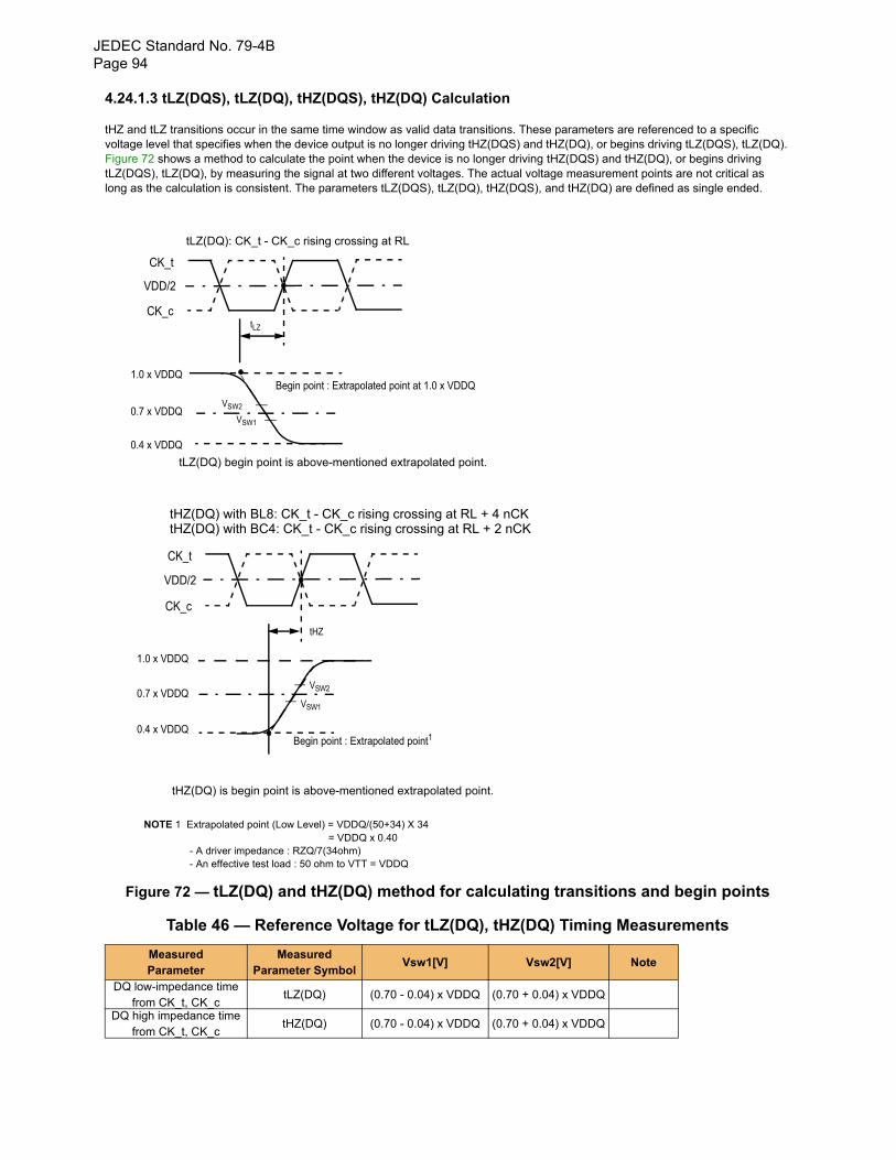
JEDEC Standard No. 79-4BPage 94
4.24.1.3 tLZ(DQS), tLZ(DQ), tHZ(DQS), tHZ(DQ) Calculation
tHZ and tLZ transitions occur in the same time window as valid data transitions. These parameters are referenced to a specific voltage level that specifies when the device output is no longer driving tHZ(DQS) and tHZ(DQ), or begins driving tLZ(DQS), tLZ(DQ). Figure 72 shows a method to calculate the point when the device is no longer driving tHZ(DQS) and tHZ(DQ), or begins driving tLZ(DQS), tLZ(DQ), by measuring the signal at two different voltages. The actual voltage measurement points are not critical aslong as the calculation is consistent. The parameters tLZ(DQS), tLZ(DQ), tHZ(DQS), and tHZ(DQ) are defined as single ended.
Figure 72 — tLZ(DQ) and tHZ(DQ) method for calculating transitions and begin points
Table 46 — Reference Voltage for tLZ(DQ), tHZ(DQ) Timing Measurements
MeasuredParameter
MeasuredParameter Symbol
Vsw1[V] Vsw2[V] Note
DQ low-impedance time from CK_t, CK_c
tLZ(DQ) (0.70 - 0.04) x VDDQ (0.70 + 0.04) x VDDQ
DQ high impedance time from CK_t, CK_c
tHZ(DQ) (0.70 - 0.04) x VDDQ (0.70 + 0.04) x VDDQ
CK_t
CK_c
Begin point : Extrapolated point at 1.0 x VDDQ
tLZ(DQ): CK_t - CK_c rising crossing at RL
tLZ
VSW1
VSW2
tLZ(DQ) begin point is above-mentioned extrapolated point.
CK_t
CK_c
VSW1
VSW2
tHZ
Begin point : Extrapolated point1
tHZ(DQ) is begin point is above-mentioned extrapolated point.
tHZ(DQ) with BL8: CK_t - CK_c rising crossing at RL + 4 nCK tHZ(DQ) with BC4: CK_t - CK_c rising crossing at RL + 2 nCK
NOTE 1 Extrapolated point (Low Level) = VDDQ/(50+34) X 34
- A driver impedance : RZQ/7(34ohm) - An effective test load : 50 ohm to VTT = VDDQ
1.0 x VDDQ
0.7 x VDDQ
0.4 x VDDQ
1.0 x VDDQ
0.7 x VDDQ
0.4 x VDDQ
= VDDQ x 0.40
VDD/2
VDD/2
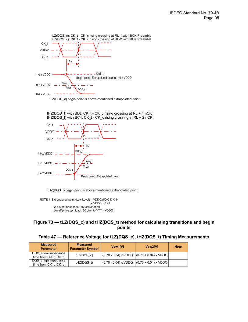
JEDEC Standard No. 79-4B Page 95
Figure 73 — tLZ(DQS_c) and tHZ(DQS_t) method for calculating transitions and begin points
Table 47 — Reference Voltage for tLZ(DQS_c), tHZ(DQS_t) Timing Measurements
MeasuredParameter
MeasuredParameter Symbol
Vsw1[V] Vsw2[V] Note
DQS_c low-impedance time from CK_t, CK_c
tLZ(DQS_c) (0.70 - 0.04) x VDDQ (0.70 + 0.04) x VDDQ
DQS_t high impedance time from CK_t, CK_c
tHZ(DQS_t) (0.70 - 0.04) x VDDQ (0.70 + 0.04) x VDDQ
CK_t
CK_c
Begin point : Extrapolated point at 1.0 x VDDQ
tLZ(DQS_c): CK_t - CK_c rising crossing at RL-1 with 1tCK Preamble
tLZ
VSW1
VSW2
tLZ(DQS_c) begin point is above-mentioned extrapolated point.
CK_t
CK_c
VSW1
VSW2
tHZ
Begin point : Extrapolated point1
tHZ(DQS_t) begin point is above-mentioned extrapolated point.
tHZ(DQS_t) with BL8: CK_t - CK_c rising crossing at RL + 4 nCK tHZ(DQS_t) with BC4: CK_t - CK_c rising crossing at RL + 2 nCK
NOTE 1 Extrapolated point (Low Level) = VDDQ/(50+34) X 34
- A driver impedance : RZQ/7(34ohm) - An effective test load : 50 ohm to VTT = VDDQ
1.0 x VDDQ
0.7 x VDDQ
0.4 x VDDQ
1.0 x VDDQ
0.7 x VDDQ
0.4 x VDDQ
= VDDQ x 0.40
VDD/2
VDD/2
tLZ(DQS_c): CK_t - CK_c rising crossing at RL-2 with 2tCK Preamble
DQS_c
DQS_t
DQS_t
DQS_c
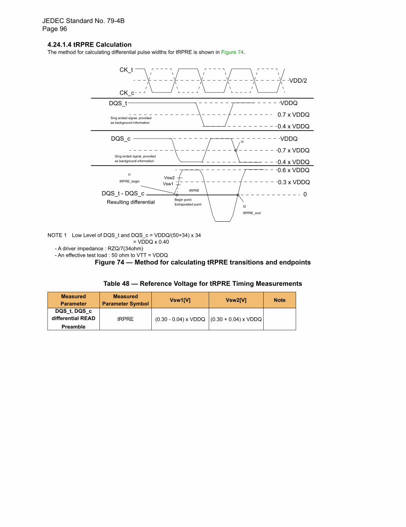
JEDEC Standard No. 79-4BPage 96
4.24.1.4 tRPRE CalculationThe method for calculating differential pulse widths for tRPRE is shown in Figure 74.
NOTE 1 Low Level of DQS_t and DQS_c = VDDQ/(50+34) x 34 = VDDQ x 0.40 - A driver impedance : RZQ/7(34ohm) - An effective test load : 50 ohm to VTT = VDDQ
Figure 74 — Method for calculating tRPRE transitions and endpoints
Table 48 — Reference Voltage for tRPRE Timing Measurements
MeasuredParameter
MeasuredParameter Symbol
Vsw1[V] Vsw2[V] Note
DQS_t, DQS_c differential READ
Preamble tRPRE (0.30 - 0.04) x VDDQ (0.30 + 0.04) x VDDQ
CK_t
CK_c
Resulting differential t2
tRPRE_end
t1
tRPRE_begin
DQS_t - DQS_c 0
VDD/2
0.7 x VDDQ
DQS_t
DQS_c
Vsw2
Vsw1
tRPRE
Sing ended signal, provided
as background information
Sing ended signal, provided
as background information
Begin point:
Extrapolated point
VDDQ
0.4 x VDDQ
0.7 x VDDQ
VDDQ
0.4 x VDDQ
tc
0.6 x VDDQ
0.3 x VDDQ
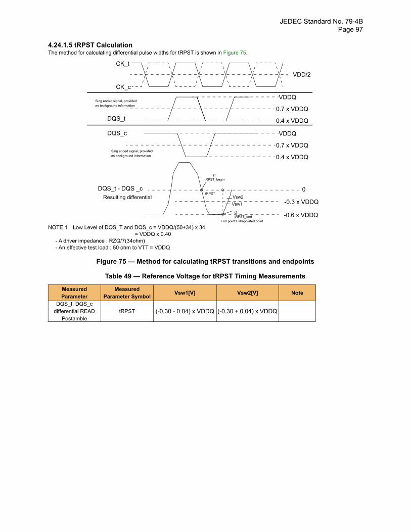
JEDEC Standard No. 79-4B Page 97
4.24.1.5 tRPST CalculationThe method for calculating differential pulse widths for tRPST is shown in Figure 75.
NOTE 1 Low Level of DQS_T and DQS_c = VDDQ/(50+34) x 34 = VDDQ x 0.40 - A driver impedance : RZQ/7(34ohm) - An effective test load : 50 ohm to VTT = VDDQ
Figure 75 — Method for calculating tRPST transitions and endpoints
Table 49 — Reference Voltage for tRPST Timing Measurements
MeasuredParameter
MeasuredParameter Symbol
Vsw1[V] Vsw2[V] Note
DQS_t, DQS_c differential READ
Postamble tRPST (-0.30 - 0.04) x VDDQ (-0.30 + 0.04) x VDDQ
CK_t
CK_c
Resulting differential
t2tRPST_end
t1tRPST_begin
DQS_t - DQS _c 0
VDD/2
DQS_t
DQS_c
Vsw2
Vsw1
tRPST
Sing ended signal, provided
as background information
Sing ended signal, provided
as background information
End point:Extrapolated point
0.7 x VDDQ
VDDQ
0.4 x VDDQ
0.7 x VDDQ
VDDQ
0.4 x VDDQ
-0.3 x VDDQ
-0.6 x VDDQ
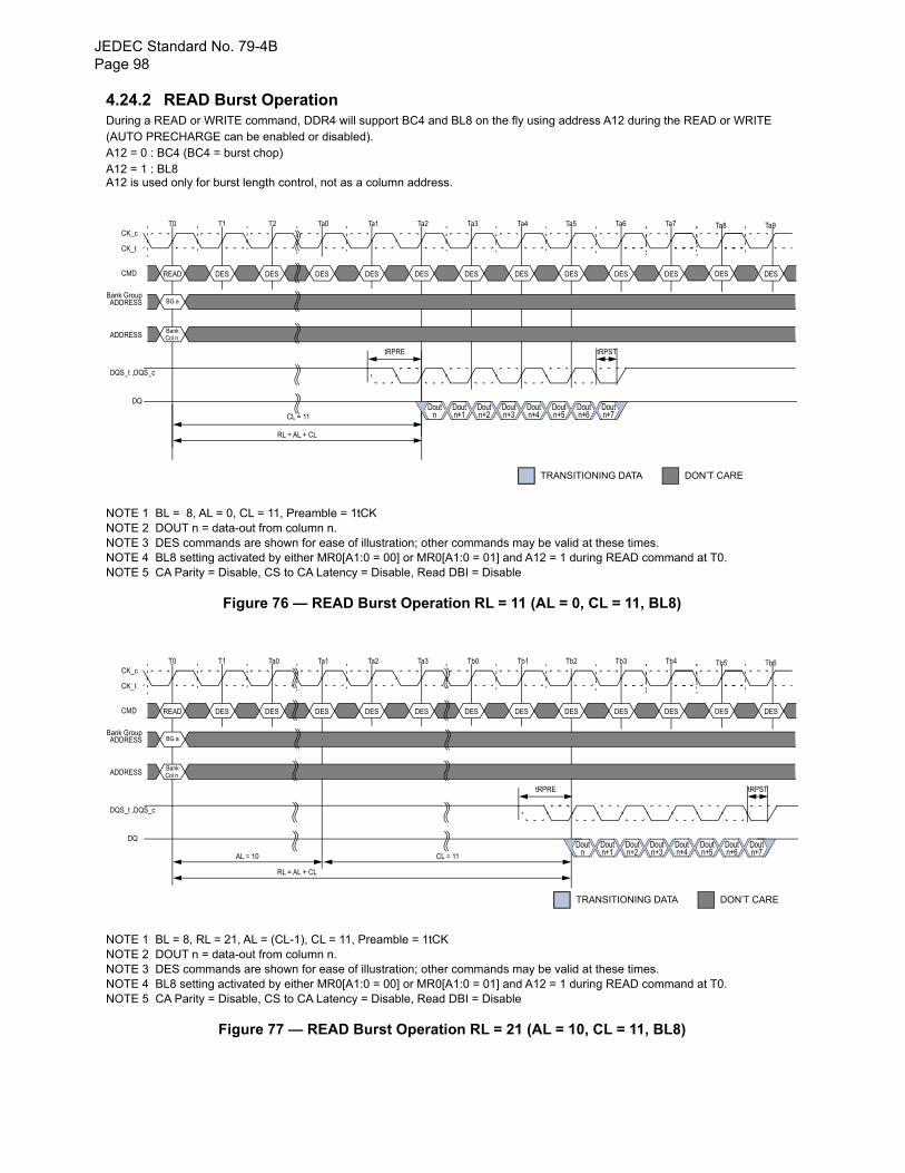
JEDEC Standard No. 79-4BPage 98
4.24.2 READ Burst OperationDuring a READ or WRITE command, DDR4 will support BC4 and BL8 on the fly using address A12 during the READ or WRITE (AUTO PRECHARGE can be enabled or disabled).A12 = 0 : BC4 (BC4 = burst chop)A12 = 1 : BL8A12 is used only for burst length control, not as a column address.
NOTE 1 BL = 8, AL = 0, CL = 11, Preamble = 1tCKNOTE 2 DOUT n = data-out from column n.NOTE 3 DES commands are shown for ease of illustration; other commands may be valid at these times.NOTE 4 BL8 setting activated by either MR0[A1:0 = 00] or MR0[A1:0 = 01] and A12 = 1 during READ command at T0.NOTE 5 CA Parity = Disable, CS to CA Latency = Disable, Read DBI = Disable
Figure 76 — READ Burst Operation RL = 11 (AL = 0, CL = 11, BL8)
NOTE 1 BL = 8, RL = 21, AL = (CL-1), CL = 11, Preamble = 1tCKNOTE 2 DOUT n = data-out from column n.NOTE 3 DES commands are shown for ease of illustration; other commands may be valid at these times.NOTE 4 BL8 setting activated by either MR0[A1:0 = 00] or MR0[A1:0 = 01] and A12 = 1 during READ command at T0.NOTE 5 CA Parity = Disable, CS to CA Latency = Disable, Read DBI = Disable
Figure 77 — READ Burst Operation RL = 21 (AL = 10, CL = 11, BL8)
READ
CK_c
CK_t
CMD
DQS_t ,DQS_c
DQ
T0 T1 Ta0 Ta1 Ta2 Ta3T2 Ta4 Ta5 Ta6 Ta7
DES DES DES DES DES DES DES DES DES DES
BG aADDRESS
tRPRE tRPST
CL = 11
RL = AL + CL
Ta8 Ta9
DES DES
Bank Group
BankADDRESS Col n
Doutn
Doutn+2
Doutn+3
Doutn+1
Doutn+4
Doutn+5
Doutn+6
Doutn+7
DON’T CARETRANSITIONING DATA
READ
CK_c
CK_t
CMD
DQS_t ,DQS_c
DQ
T0 T1 Ta1 Ta2 Ta3 Tb0Ta0 Tb1 Tb2 Tb3 Tb4
DES DES DES DES DES DES DES DES DES DES
BG aADDRESS
tRPRE tRPST
CL = 11
RL = AL + CL
Tb5 Tb6
DES DES
Bank Group
BankADDRESS Col n
Doutn
Doutn+2
Doutn+3
Doutn+1
Doutn+4
Doutn+5
Doutn+6
Doutn+7
DON’T CARETRANSITIONING DATA
AL = 10
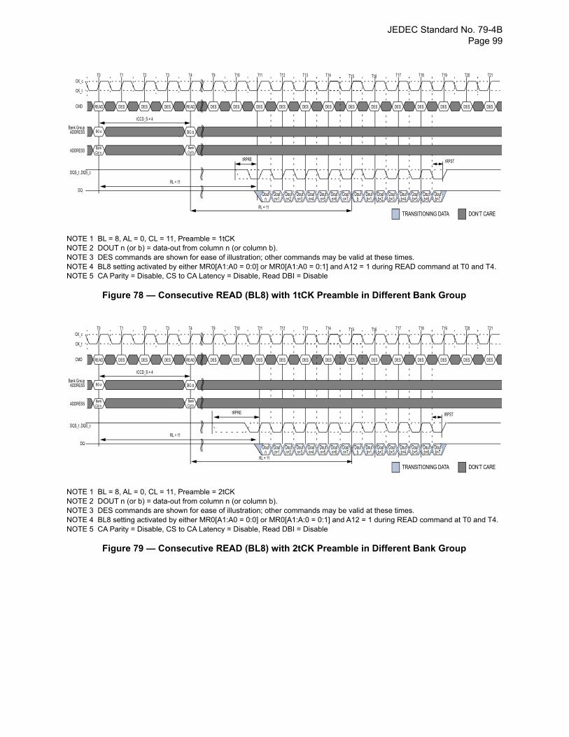
JEDEC Standard No. 79-4B Page 99
NOTE 1 BL = 8, AL = 0, CL = 11, Preamble = 1tCKNOTE 2 DOUT n (or b) = data-out from column n (or column b).NOTE 3 DES commands are shown for ease of illustration; other commands may be valid at these times.NOTE 4 BL8 setting activated by either MR0[A1:A0 = 0:0] or MR0[A1:A0 = 0:1] and A12 = 1 during READ command at T0 and T4.NOTE 5 CA Parity = Disable, CS to CA Latency = Disable, Read DBI = Disable
Figure 78 — Consecutive READ (BL8) with 1tCK Preamble in Different Bank Group
NOTE 1 BL = 8, AL = 0, CL = 11, Preamble = 2tCKNOTE 2 DOUT n (or b) = data-out from column n (or column b).NOTE 3 DES commands are shown for ease of illustration; other commands may be valid at these times.NOTE 4 BL8 setting activated by either MR0[A1:A0 = 0:0] or MR0[A1:A:0 = 0:1] and A12 = 1 during READ command at T0 and T4.NOTE 5 CA Parity = Disable, CS to CA Latency = Disable, Read DBI = Disable
Figure 79 — Consecutive READ (BL8) with 2tCK Preamble in Different Bank Group
READ
CK_c
CK_t
CMD
DQS_t ,DQS_c
DQ
T0 T1 T3 T4 T9 T10T2 T11 T12 T13 T14
DES DES DES READ DES DES DES DES DES DES
BG aADDRESS
tRPRE tRPST
RL = 11
T15 T16
DES DES
Bank Group
BankADDRESS Col n
Doutn
Doutn+2
Doutn+3
Doutn+1
Doutn+4
Doutn+5
Doutn+6
Doutn+7
DON’T CARETRANSITIONING DATA
T17 T18 T20 T21T19
DES DES DES DES DES
BG b
BankCol b
Doutb
Doutb+2
Doutb+3
Doutb+1
Doutb+4
Doutb+5
Doutb+6
Doutb+7
RL = 11
tCCD_S = 4
READ
CK_c
CK_t
CMD
DQS_t ,DQS_c
DQ
T0 T1 T3 T4 T9 T10T2 T11 T12 T13 T14
DES DES DES READ DES DES DES DES DES DES
BG aADDRESS
tRPRE tRPST
RL = 11
T15 T16
DES DES
Bank Group
BankADDRESS Col n
Doutn
Doutn+2
Doutn+3
Doutn+1
Doutn+4
Doutn+5
Doutn+6
Doutn+7
DON’T CARETRANSITIONING DATA
T17 T18 T20 T21T19
DES DES DES DES DES
BG b
BankCol b
Doutb
Doutb+2
Doutb+3
Doutb+1
Doutb+4
Doutb+5
Doutb+6
Doutb+7
tCCD_S = 4
RL = 11
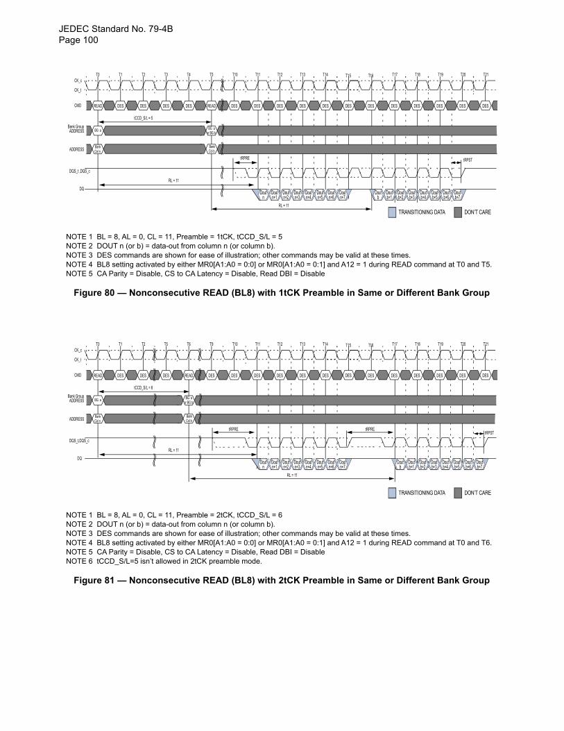
JEDEC Standard No. 79-4BPage 100
NOTE 1 BL = 8, AL = 0, CL = 11, Preamble = 1tCK, tCCD_S/L = 5NOTE 2 DOUT n (or b) = data-out from column n (or column b).NOTE 3 DES commands are shown for ease of illustration; other commands may be valid at these times.NOTE 4 BL8 setting activated by either MR0[A1:A0 = 0:0] or MR0[A1:A0 = 0:1] and A12 = 1 during READ command at T0 and T5.NOTE 5 CA Parity = Disable, CS to CA Latency = Disable, Read DBI = Disable
Figure 80 — Nonconsecutive READ (BL8) with 1tCK Preamble in Same or Different Bank Group
NOTE 1 BL = 8, AL = 0, CL = 11, Preamble = 2tCK, tCCD_S/L = 6NOTE 2 DOUT n (or b) = data-out from column n (or column b).NOTE 3 DES commands are shown for ease of illustration; other commands may be valid at these times.NOTE 4 BL8 setting activated by either MR0[A1:A0 = 0:0] or MR0[A1:A0 = 0:1] and A12 = 1 during READ command at T0 and T6.NOTE 5 CA Parity = Disable, CS to CA Latency = Disable, Read DBI = DisableNOTE 6 tCCD_S/L=5 isn’t allowed in 2tCK preamble mode.
Figure 81 — Nonconsecutive READ (BL8) with 2tCK Preamble in Same or Different Bank Group
READ
CK_c
CK_t
CMD
DQS_t ,DQS_c
DQ
T0 T1 T3 T4 T5 T10T2 T11 T12 T13 T14
DES DES DES DES READ DES DES DES DES DES
BG aADDRESS
tRPRE tRPST
RL = 11
T15 T16
DES DES
Bank Group
BankADDRESS Col n
Doutn
Doutn+2
Doutn+3
Doutn+1
Doutn+4
Doutn+5
Doutn+6
Doutn+7
DON’T CARETRANSITIONING DATA
T17 T18 T20 T21T19
DES DES DES DES DES
BG a
BankCol b
Doutb
Doutb+2
Doutb+3
Doutb+1
Doutb+4
Doutb+5
Doutb+6
Doutb+7
RL = 11
tCCD_S/L = 5
or BG b
READ
CK_c
CK_t
CMD
DQS_t,DQS_c
DQ
T0 T1 T5 T6 T9 T10T2 T11 T12 T13 T14
DES DES DES READ DES DES DES DES DES DES
BG aADDRESS
tRPREtRPST
RL = 11
T15 T16
DES DES
Bank Group
BankADDRESS Col n
Doutn
Doutn+2
Doutn+3
Doutn+1
Doutn+4
Doutn+5
Doutn+6
Doutn+7
DON’T CARETRANSITIONING DATA
T17 T18 T20 T21T19
DES DES DES DES DES
BG a
BankCol b
Doutb
Doutb+2
Doutb+3
Doutb+1
Doutb+4
Doutb+5
Doutb+6
Doutb+7
RL = 11
tCCD_S/L = 6
or BG b
tRPRE
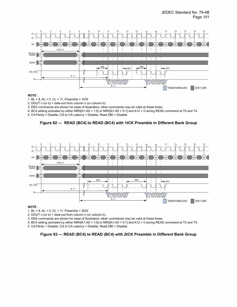
JEDEC Standard No. 79-4B Page 101
NOTE :1. BL = 8, AL = 0, CL = 11, Preamble = 1tCK2. DOUT n (or b) = data-out from column n (or column b).3. DES commands are shown for ease of illustration; other commands may be valid at these times.4. BC4 setting activated by either MR0[A1:A0 = 1:0] or MR0[A1:A0 = 0:1] and A12 = 0 during READ command at T0 and T4.5. CA Parity = Disable, CS to CA Latency = Disable, Read DBI = Disable
Figure 82 — READ (BC4) to READ (BC4) with 1tCK Preamble in Different Bank Group
NOTE :1. BL = 8, AL = 0, CL = 11, Preamble = 2tCK2. DOUT n (or b) = data-out from column n (or column b).3. DES commands are shown for ease of illustration; other commands may be valid at these times.4. BC4 setting activated by either MR0[A1:A0 = 1:0] or MR0[A1:A0 = 0:1] and A12 = 0 during READ command at T0 and T4.5. CA Parity = Disable, CS to CA Latency = Disable, Read DBI = Disable
Figure 83 — READ (BC4) to READ (BC4) with 2tCK Preamble in Different Bank Group
READ
CK_c
CK_t
CMD
DQS_t ,DQS_c
DQ
T0 T1 T3 T4 T9 T10T2 T11 T12 T13 T14
DES DES DES READ DES DES DES DES DES DES
BG aADDRESS
tRPREtRPST
RL = 11
T15 T16
DES DES
Bank Group
BankADDRESS Col n
Doutn
Doutn+2
Doutn+3
Doutn+1
DON’T CARETRANSITIONING DATA
T17 T18 T20 T21T19
DES DES DES DES DES
BankCol b
RL = 11
tCCD_S = 4
BG b
tRPREtRPST
Doutb
Doutb+2
Doutb+3
Doutb+1
READ
CK_c
CK_t
CMD
DQS_t ,DQS_c
DQ
T0 T1 T3 T4 T9 T10T2 T11 T12 T13 T14
DES DES DES READ DES DES DES DES DES DES
BG aADDRESS
tRPRE
RL = 11
T15 T16
DES DES
Bank Group
BankADDRESS Col n
Doutn
Doutn+2
Doutn+3
Doutn+1
DON’T CARETRANSITIONING DATA
T17 T18 T20 T21T19
DES DES DES DES DES
BankCol b
RL = 11
tCCD_S = 4
BG b
tRPREtRPST
Doutb
Doutb+2
Doutb+3
Doutb+1
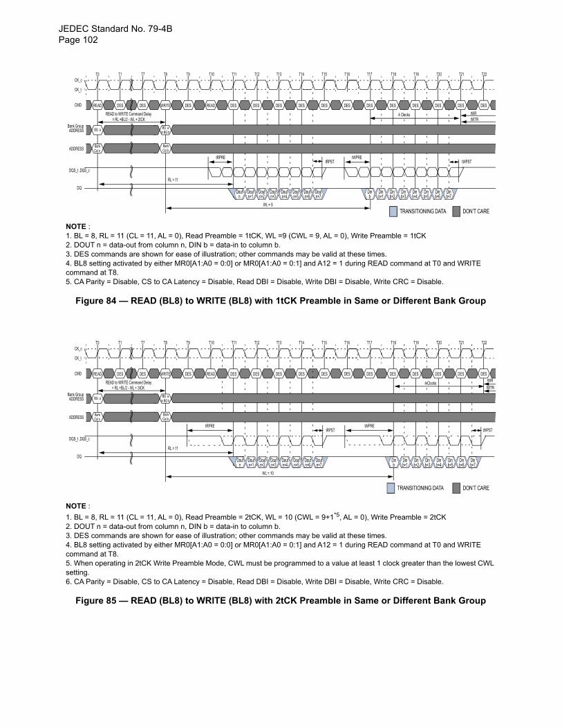
JEDEC Standard No. 79-4BPage 102
NOTE :1. BL = 8, RL = 11 (CL = 11, AL = 0), Read Preamble = 1tCK, WL =9 (CWL = 9, AL = 0), Write Preamble = 1tCK2. DOUT n = data-out from column n, DIN b = data-in to column b.3. DES commands are shown for ease of illustration; other commands may be valid at these times.4. BL8 setting activated by either MR0[A1:A0 = 0:0] or MR0[A1:A0 = 0:1] and A12 = 1 during READ command at T0 and WRITE command at T8.5. CA Parity = Disable, CS to CA Latency = Disable, Read DBI = Disable, Write DBI = Disable, Write CRC = Disable.
Figure 84 — READ (BL8) to WRITE (BL8) with 1tCK Preamble in Same or Different Bank Group
NOTE :
1. BL = 8, RL = 11 (CL = 11, AL = 0), Read Preamble = 2tCK, WL = 10 (CWL = 9+1*5, AL = 0), Write Preamble = 2tCK2. DOUT n = data-out from column n, DIN b = data-in to column b.3. DES commands are shown for ease of illustration; other commands may be valid at these times.4. BL8 setting activated by either MR0[A1:A0 = 0:0] or MR0[A1:A0 = 0:1] and A12 = 1 during READ command at T0 and WRITE command at T8.5. When operating in 2tCK Write Preamble Mode, CWL must be programmed to a value at least 1 clock greater than the lowest CWL setting.6. CA Parity = Disable, CS to CA Latency = Disable, Read DBI = Disable, Write DBI = Disable, Write CRC = Disable.
Figure 85 — READ (BL8) to WRITE (BL8) with 2tCK Preamble in Same or Different Bank Group
READ
CK_c
CK_t
CMD
DQS_t ,DQS_c
DQ
T0 T1 T8 T9 T10 T11T7 T12 T13 T14 T15
DES DES WRITE DES READ DES DES DES DES DES
BG aADDRESS
tRPREtRPST
RL = 11
T16 T17
DES DES
Bank Group
BankADDRESS Col n
Doutn
Doutn+2
Doutn+3
Doutn+1
Doutn+4
Doutn+5
Doutn+6
Doutn+7
DON’T CARE
T18 T19 T21 T22T20
DES DES DES DES DES
BG a
BankCol b
Dinb
Dinb+2
Dinb+3
Dinb+1
Dinb+4
Dinb+5
Dinb+6
Dinb+7
WL = 9
READ to WRITE Command Delay
or BG b
= RL +BL/2 - WL + 2tCK
tWPREtWPST
4 Clocks tWRtWTR
TRANSITIONING DATA
READ
CK_c
CK_t
CMD
DQS_t ,DQS_c
DQ
T0 T1 T8 T9 T10 T11T7 T12 T13 T14 T15
DES DES WRITE DES READ DES DES DES DES DES
BG aADDRESS
tRPREtRPST
RL = 11
T16 T17
DES DES
Bank Group
BankADDRESS Col n
Doutn
Doutn+2
Doutn+3
Doutn+1
Doutn+4
Doutn+5
Doutn+6
Doutn+7
DON’T CARETRANSITIONING DATA
T18 T19 T21 T22T20
DES DES DES DES DES
BG a
BankCol b
Dinb
Dinb+2
Dinb+3
Dinb+1
Dinb+4
Dinb+5
Dinb+6
Dinb+7
WL = 10
READ to WRITE Command Delay
or BG b
= RL +BL/2 - WL + 3tCK
tWPREtWPST
4 Clocks tWR
tWTR
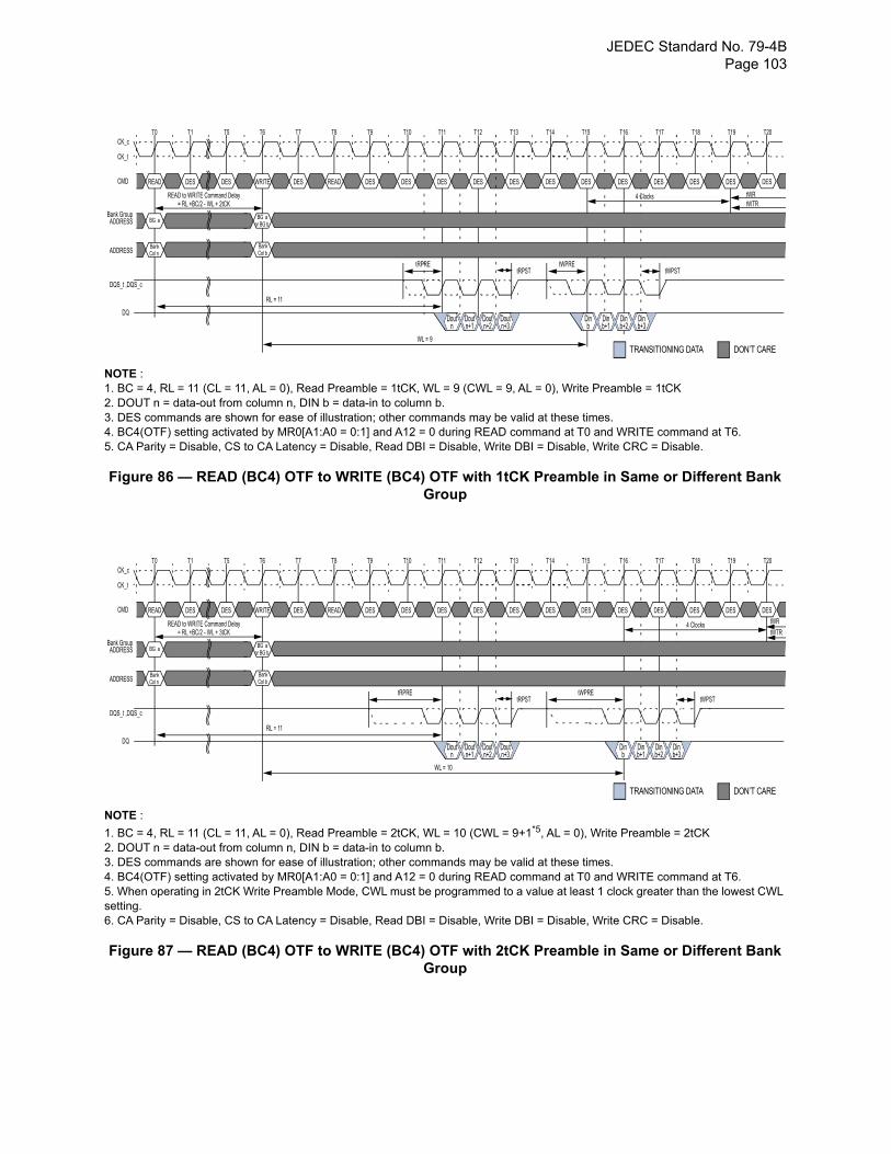
JEDEC Standard No. 79-4B Page 103
NOTE :1. BC = 4, RL = 11 (CL = 11, AL = 0), Read Preamble = 1tCK, WL = 9 (CWL = 9, AL = 0), Write Preamble = 1tCK2. DOUT n = data-out from column n, DIN b = data-in to column b.3. DES commands are shown for ease of illustration; other commands may be valid at these times.4. BC4(OTF) setting activated by MR0[A1:A0 = 0:1] and A12 = 0 during READ command at T0 and WRITE command at T6.5. CA Parity = Disable, CS to CA Latency = Disable, Read DBI = Disable, Write DBI = Disable, Write CRC = Disable.
Figure 86 — READ (BC4) OTF to WRITE (BC4) OTF with 1tCK Preamble in Same or Different Bank Group
NOTE :
1. BC = 4, RL = 11 (CL = 11, AL = 0), Read Preamble = 2tCK, WL = 10 (CWL = 9+1*5, AL = 0), Write Preamble = 2tCK2. DOUT n = data-out from column n, DIN b = data-in to column b.3. DES commands are shown for ease of illustration; other commands may be valid at these times.4. BC4(OTF) setting activated by MR0[A1:A0 = 0:1] and A12 = 0 during READ command at T0 and WRITE command at T6.5. When operating in 2tCK Write Preamble Mode, CWL must be programmed to a value at least 1 clock greater than the lowest CWL setting.6. CA Parity = Disable, CS to CA Latency = Disable, Read DBI = Disable, Write DBI = Disable, Write CRC = Disable.
Figure 87 — READ (BC4) OTF to WRITE (BC4) OTF with 2tCK Preamble in Same or Different Bank Group
READ
CK_c
CK_t
CMD
DQS_t ,DQS_c
DQ
T0 T1 T6 T7 T8 T9T5 T10 T11 T12 T13
DES DES WRITE DES READ DES DES DES DES DES
BG aADDRESS
tRPST
RL = 11
T14 T15
DES DES
Bank Group
BankADDRESS Col n
DON’T CARETRANSITIONING DATA
T16 T17 T19 T20T18
DES DES DES DES DES
BG a
BankCol b
WL = 9
READ to WRITE Command Delay
or BG b
= RL +BC/2 - WL + 2tCK
tWPREtWPST
4 Clocks tWRtWTR
tRPRE
Doutn
Doutn+2
Doutn+3
Doutn+1
Dinb
Dinb+2
Dinb+3
Dinb+1
READ
CK_c
CK_t
CMD
DQS_t ,DQS_c
DQ
T0 T1 T6 T7 T8 T9T5 T10 T11 T12 T13
DES DES WRITE DES READ DES DES DES DES DES
BG aADDRESS
tRPST
RL = 11
T14 T15
DES DES
Bank Group
BankADDRESS Col n
DON’T CARETRANSITIONING DATA
T16 T17 T19 T20T18
DES DES DES DES DES
BG a
BankCol b
WL = 10
READ to WRITE Command Delay
or BG b
= RL +BC/2 - WL + 3tCK
tWPREtWPST
4 Clocks tWR
tWTR
tRPRE
Doutn
Doutn+2
Doutn+3
Doutn+1
Dinb
Dinb+2
Dinb+3
Dinb+1
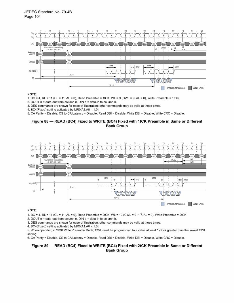
JEDEC Standard No. 79-4BPage 104
NOTE:1. BC = 4, RL = 11 (CL = 11, AL = 0), Read Preamble = 1tCK, WL = 9 (CWL = 9, AL = 0), Write Preamble = 1tCK2. DOUT n = data-out from column n, DIN b = data-in to column b.3. DES commands are shown for ease of illustration; other commands may be valid at these times.4. BC4(Fixed) setting activated by MR0[A1:A0 = 1:0].5. CA Parity = Disable, CS to CA Latency = Disable, Read DBI = Disable, Write DBI = Disable, Write CRC = Disable.
Figure 88 — READ (BC4) Fixed to WRITE (BC4) Fixed with 1tCK Preamble in Same or Different Bank Group
NOTE:
1. BC = 4, RL = 11 (CL = 11, AL = 0), Read Preamble = 2tCK, WL = 10 (CWL = 9+1*5, AL = 0), Write Preamble = 2tCK2. DOUT n = data-out from column n, DIN b = data-in to column b.3. DES commands are shown for ease of illustration; other commands may be valid at these times.4. BC4(Fixed) setting activated by MR0[A1:A0 = 1:0].5. When operating in 2tCK Write Preamble Mode, CWL must be programmed to a value at least 1 clock greater than the lowest CWL setting.6. CA Parity = Disable, CS to CA Latency = Disable, Read DBI = Disable, Write DBI = Disable, Write CRC = Disable.
Figure 89 — READ (BC4) Fixed to WRITE (BC4) Fixed with 2tCK Preamble in Same or Different Bank Group
READ
CK_c
CK_t
CMD
DQS_t ,DQS_c
DQ
T0 T1 T6 T7 T8 T9T5 T10 T11 T12 T13
DES DES WRITE DES DES DES DES DES DES
BG aADDRESS
tRPST
RL = 11
T14 T15
DES DES
Bank Group
BankADDRESS Col n
DON’T CARETRANSITIONING DATA
T16 T17 T19 T20T18
DES DES DES DES DES
BG a
BankCol b
WL = 9
READ to WRITE Command Delay
or BG b
= RL +BC/2 - WL + 2tCK
tWPREtWPST
2 Clocks tWRtWTR
tRPRE
Doutn
Doutn+2
Doutn+3
Doutn+1
Dinb
Dinb+2
Dinb+3
Dinb+1
DES
READ
CK_c
CK_t
CMD
DQS_t ,DQS_c
DQ
T0 T1 T6 T7 T8 T9T5 T10 T11 T12 T13
DES DES WRITE DES DES DES DES DES DES
BG aADDRESS
tRPST
RL = 11
T14 T15
DES DES
Bank Group
BankADDRESS Col n
DON’T CARETRANSITIONING DATA
T16 T17 T19 T20T18
DES DES DES DES DES
BG a
BankCol b
WL = 10
READ to WRITE Command Delay
or BG b
= RL +BC/2 - WL + 3tCK
tWPREtWPST
2 Clocks tWR
tWTR
tRPRE
Doutn
Doutn+2
Doutn+3
Doutn+1
Dinb
Dinb+2
Dinb+3
Dinb+1
DES
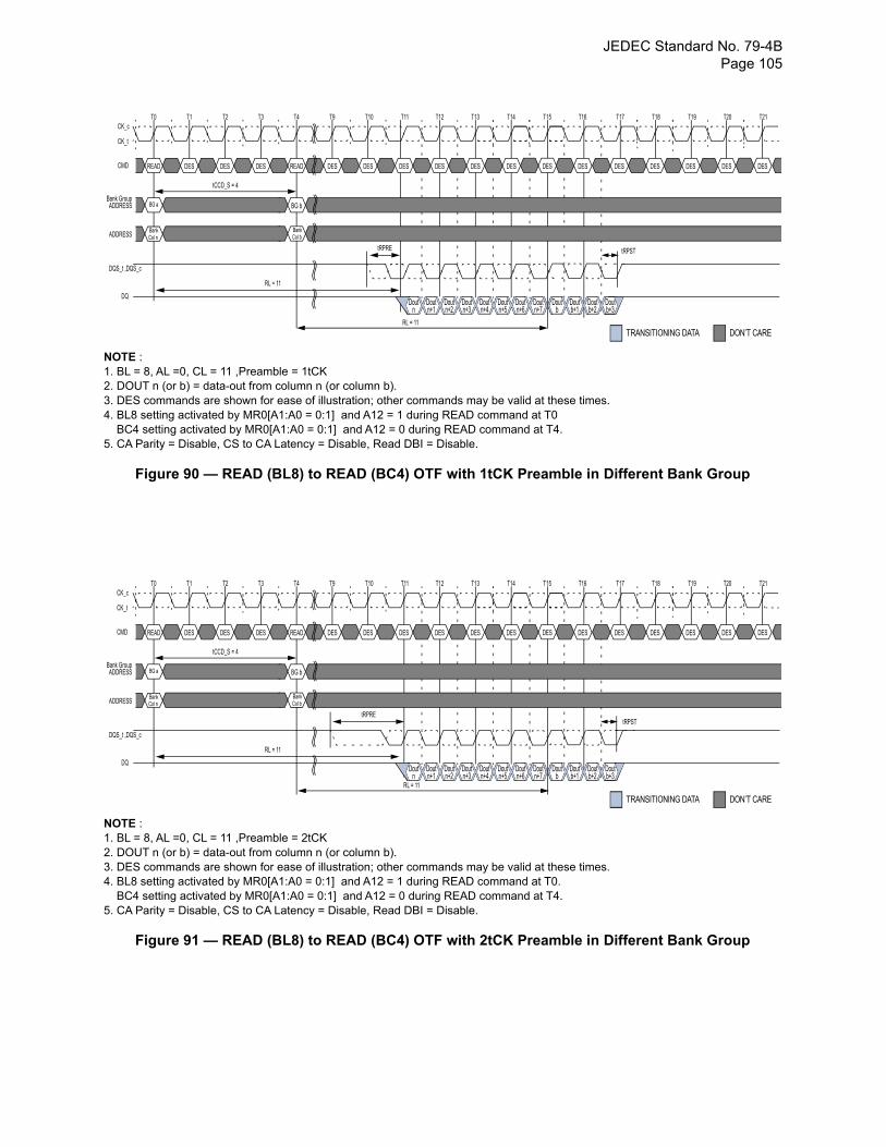
JEDEC Standard No. 79-4B Page 105
NOTE :1. BL = 8, AL =0, CL = 11 ,Preamble = 1tCK2. DOUT n (or b) = data-out from column n (or column b).3. DES commands are shown for ease of illustration; other commands may be valid at these times.4. BL8 setting activated by MR0[A1:A0 = 0:1] and A12 = 1 during READ command at T0 BC4 setting activated by MR0[A1:A0 = 0:1] and A12 = 0 during READ command at T4.5. CA Parity = Disable, CS to CA Latency = Disable, Read DBI = Disable.
Figure 90 — READ (BL8) to READ (BC4) OTF with 1tCK Preamble in Different Bank Group
NOTE :1. BL = 8, AL =0, CL = 11 ,Preamble = 2tCK2. DOUT n (or b) = data-out from column n (or column b).3. DES commands are shown for ease of illustration; other commands may be valid at these times.4. BL8 setting activated by MR0[A1:A0 = 0:1] and A12 = 1 during READ command at T0. BC4 setting activated by MR0[A1:A0 = 0:1] and A12 = 0 during READ command at T4.5. CA Parity = Disable, CS to CA Latency = Disable, Read DBI = Disable.
Figure 91 — READ (BL8) to READ (BC4) OTF with 2tCK Preamble in Different Bank Group
READ
CK_c
CK_t
CMD
DQS_t ,DQS_c
DQ
T0 T1 T3 T4 T9 T10T2 T11 T12 T13 T14
DES DES DES READ DES DES DES DES DES DES
BG aADDRESS
tRPRE tRPST
RL = 11
T15 T16
DES DES
Bank Group
BankADDRESS Col n
Doutn
Doutn+2
Doutn+3
Doutn+1
Doutn+4
Doutn+5
Doutn+6
Doutn+7
DON’T CARETRANSITIONING DATA
T17 T18 T20 T21T19
DES DES DES DES DES
BG b
BankCol b
Doutb
Doutb+2
Doutb+3
Doutb+1
RL = 11
tCCD_S = 4
READ
CK_c
CK_t
CMD
DQS_t ,DQS_c
DQ
T0 T1 T3 T4 T9 T10T2 T11 T12 T13 T14
DES DES DES READ DES DES DES DES DES DES
BG aADDRESS
tRPREtRPST
RL = 11
T15 T16
DES DES
Bank Group
BankADDRESS Col n
Doutn
Doutn+2
Doutn+3
Doutn+1
Doutn+4
Doutn+5
Doutn+6
Doutn+7
DON’T CARETRANSITIONING DATA
T17 T18 T20 T21T19
DES DES DES DES DES
BG b
BankCol b
Doutb
Doutb+2
Doutb+3
Doutb+1
tCCD_S = 4
RL = 11
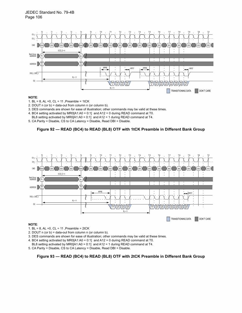
JEDEC Standard No. 79-4BPage 106
NOTE:1. BL = 8, AL =0, CL = 11 ,Preamble = 1tCK2. DOUT n (or b) = data-out from column n (or column b).3. DES commands are shown for ease of illustration; other commands may be valid at these times.4. BC4 setting activated by MR0[A1:A0 = 0:1] and A12 = 0 during READ command at T0. BL8 setting activated by MR0[A1:A0 = 0:1] and A12 = 1 during READ command at T4.5. CA Parity = Disable, CS to CA Latency = Disable, Read DBI = Disable.
Figure 92 — READ (BC4) to READ (BL8) OTF with 1tCK Preamble in Different Bank Group
NOTE:1. BL = 8, AL =0, CL = 11 ,Preamble = 2tCK2. DOUT n (or b) = data-out from column n (or column b).3. DES commands are shown for ease of illustration; other commands may be valid at these times.4. BC4 setting activated by MR0[A1:A0 = 0:1] and A12 = 0 during READ command at T0. BL8 setting activated by MR0[A1:A0 = 0:1] and A12 = 1 during READ command at T4.5. CA Parity = Disable, CS to CA Latency = Disable, Read DBI = Disable.
Figure 93 — READ (BC4) to READ (BL8) OTF with 2tCK Preamble in Different Bank Group
READ
CK_c
CK_t
CMD
DQS_t ,DQS_c
DQ
T0 T1 T3 T4 T9 T10T2 T11 T12 T13 T14
DES DES DES READ DES DES DES DES DES DES
BG aADDRESS
tRPRE tRPST
RL = 11
T15 T16
DES DES
Bank Group
BankADDRESS Col n
DON’T CARETRANSITIONING DATA
T17 T18 T20 T21T19
DES DES DES DES DES
BG b
BankCol b
RL = 11
tCCD_S = 4
tRPREtRPST
Doutn
Doutn+2
Doutn+3
Doutn+1
Doutb
Doutb+2
Doutb+3
Doutb+1
Doutb+4
Doutb+5
Doutb+6
Doutb+7
READ
CK_c
CK_t
CMD
DQS_t ,DQS_c
DQ
T0 T1 T3 T4 T9 T10T2 T11 T12 T13 T14
DES DES DES READ DES DES DES DES DES DES
BG aADDRESS
tRPREtRPST
RL = 11
T15 T16
DES DES
Bank Group
BankADDRESS Col n
Doutn
Doutn+2
Doutn+7
Doutn+1
DON’T CARETRANSITIONING DATA
T17 T18 T20 T21T19
DES DES DES DES DES
BG b
BankCol b
Doutb
Doutb+2
Doutb+3
Doutb+1
Doutb+4
Doutb+5
Doutb+6
Doutb+7
RL = 11
tCCD_S = 4
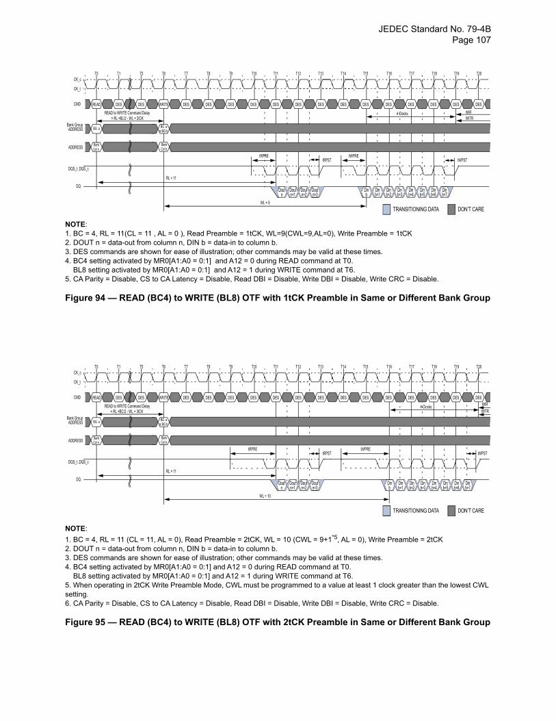
JEDEC Standard No. 79-4B Page 107
NOTE:1. BC = 4, RL = 11(CL = 11 , AL = 0 ), Read Preamble = 1tCK, WL=9(CWL=9,AL=0), Write Preamble = 1tCK2. DOUT n = data-out from column n, DIN b = data-in to column b.3. DES commands are shown for ease of illustration; other commands may be valid at these times.4. BC4 setting activated by MR0[A1:A0 = 0:1] and A12 = 0 during READ command at T0. BL8 setting activated by MR0[A1:A0 = 0:1] and A12 = 1 during WRITE command at T6.5. CA Parity = Disable, CS to CA Latency = Disable, Read DBI = Disable, Write DBI = Disable, Write CRC = Disable.
Figure 94 — READ (BC4) to WRITE (BL8) OTF with 1tCK Preamble in Same or Different Bank Group
NOTE:
1. BC = 4, RL = 11 (CL = 11, AL = 0), Read Preamble = 2tCK, WL = 10 (CWL = 9+1*5, AL = 0), Write Preamble = 2tCK2. DOUT n = data-out from column n, DIN b = data-in to column b.3. DES commands are shown for ease of illustration; other commands may be valid at these times.4. BC4 setting activated by MR0[A1:A0 = 0:1] and A12 = 0 during READ command at T0. BL8 setting activated by MR0[A1:A0 = 0:1] and A12 = 1 during WRITE command at T6.5. When operating in 2tCK Write Preamble Mode, CWL must be programmed to a value at least 1 clock greater than the lowest CWL setting.6. CA Parity = Disable, CS to CA Latency = Disable, Read DBI = Disable, Write DBI = Disable, Write CRC = Disable.
Figure 95 — READ (BC4) to WRITE (BL8) OTF with 2tCK Preamble in Same or Different Bank Group
READ
CK_c
CK_t
CMD
DQS_t ,DQS_c
DQ
T0 T1 T6 T7 T8 T9T5 T10 T11 T12 T13
DES DES WRITE DES DES DES DES DES DES DES
BG aADDRESS
tRPREtRPST
RL = 11
T14 T15
DES DES
Bank Group
BankADDRESS Col n
DON’T CARETRANSITIONING DATA
T16 T17 T19 T20T18
DES DES DES DES DES
BG a
BankCol b
Dinb
Dinb+2
Dinb+3
Dinb+1
Dinb+4
Dinb+5
Dinb+6
Dinb+7
WL = 9
READ to WRITE Command Delay
or BG b
= RL +BL/2 - WL + 2tCK
tWPREtWPST
4 Clocks tWRtWTR
Doutn
Doutn+2
Doutn+3
Doutn+1
READ
CK_c
CK_t
CMD
DQS_t ,DQS_c
DQ
T0 T1 T6 T7 T8 T9T5 T10 T11 T12 T13
DES DES WRITE DES DES DES DES DES DES DES
BG aADDRESS
tRPREtRPST
RL = 11
T14 T15
DES DES
Bank Group
BankADDRESS Col n
DON’T CARETRANSITIONING DATA
T16 T17 T19 T20T18
DES DES DES DES DES
BG a
BankCol b
Dinb
Dinb+2
Dinb+3
Dinb+1
Dinb+4
Dinb+5
Dinb+6
Dinb+7
WL = 10
READ to WRITE Command Delay
or BG b
= RL +BC/2 - WL + 3tCK
tWPREtWPST
4 Clocks tWR
tWTR
Doutn
Doutn+2
Doutn+3
Doutn+1
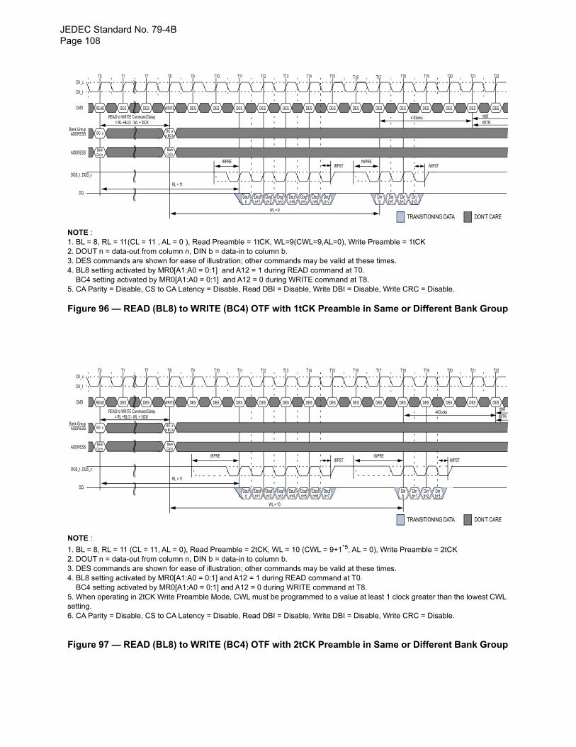
JEDEC Standard No. 79-4BPage 108
NOTE :1. BL = 8, RL = 11(CL = 11 , AL = 0 ), Read Preamble = 1tCK, WL=9(CWL=9,AL=0), Write Preamble = 1tCK2. DOUT n = data-out from column n, DIN b = data-in to column b.3. DES commands are shown for ease of illustration; other commands may be valid at these times.4. BL8 setting activated by MR0[A1:A0 = 0:1] and A12 = 1 during READ command at T0. BC4 setting activated by MR0[A1:A0 = 0:1] and A12 = 0 during WRITE command at T8.5. CA Parity = Disable, CS to CA Latency = Disable, Read DBI = Disable, Write DBI = Disable, Write CRC = Disable.
Figure 96 — READ (BL8) to WRITE (BC4) OTF with 1tCK Preamble in Same or Different Bank Group
NOTE :
1. BL = 8, RL = 11 (CL = 11, AL = 0), Read Preamble = 2tCK, WL = 10 (CWL = 9+1*5, AL = 0), Write Preamble = 2tCK2. DOUT n = data-out from column n, DIN b = data-in to column b.3. DES commands are shown for ease of illustration; other commands may be valid at these times.4. BL8 setting activated by MR0[A1:A0 = 0:1] and A12 = 1 during READ command at T0. BC4 setting activated by MR0[A1:A0 = 0:1] and A12 = 0 during WRITE command at T8.5. When operating in 2tCK Write Preamble Mode, CWL must be programmed to a value at least 1 clock greater than the lowest CWL setting.6. CA Parity = Disable, CS to CA Latency = Disable, Read DBI = Disable, Write DBI = Disable, Write CRC = Disable.
Figure 97 — READ (BL8) to WRITE (BC4) OTF with 2tCK Preamble in Same or Different Bank Group
READ
CK_c
CK_t
CMD
DQS_t ,DQS_c
DQ
T0 T1 T8 T9 T10 T11T7 T12 T13 T14 T15
DES DES WRITE DES DES DES DES DES DES DES
BG aADDRESS
tRPREtRPST
RL = 11
T16 T17
DES DES
Bank Group
BankADDRESS Col n
Doutn
Doutn+2
Doutn+3
Doutn+1
Doutn+4
Doutn+5
Doutn+6
Doutn+7
DON’T CARETRANSITIONING DATA
T18 T19 T21 T22T20
DES DES DES DES DES
BG a
BankCol b
Dinb
Dinb+2
Dinb+3
Dinb+1
WL = 9
READ to WRITE Command Delay
or BG b
= RL +BL/2 - WL + 2tCK
tWPREtWPST
4 Clocks tWRtWTR
READ
CK_c
CK_t
CMD
DQS_t ,DQS_c
DQ
T0 T1 T8 T9 T10 T11T7 T12 T13 T14 T15
DES DES WRITE DES DES DES DES DES DES DES
BG aADDRESS
tRPREtRPST
RL = 11
T16 T17
DES DES
Bank Group
BankADDRESS Col n
Doutn
Doutn+2
Doutn+3
Doutn+1
Doutn+4
Doutn+5
Doutn+6
Doutn+7
DON’T CARETRANSITIONING DATA
T18 T19 T21 T22T20
DES DES DES DES DES
BG a
BankCol b
WL = 10
READ to WRITE Command Delay
or BG b
= RL +BL/2 - WL + 3tCK
tWPREtWPST
4 Clocks tWR
tWTR
Dinb
Dinb+2
Dinb+3
Dinb+1
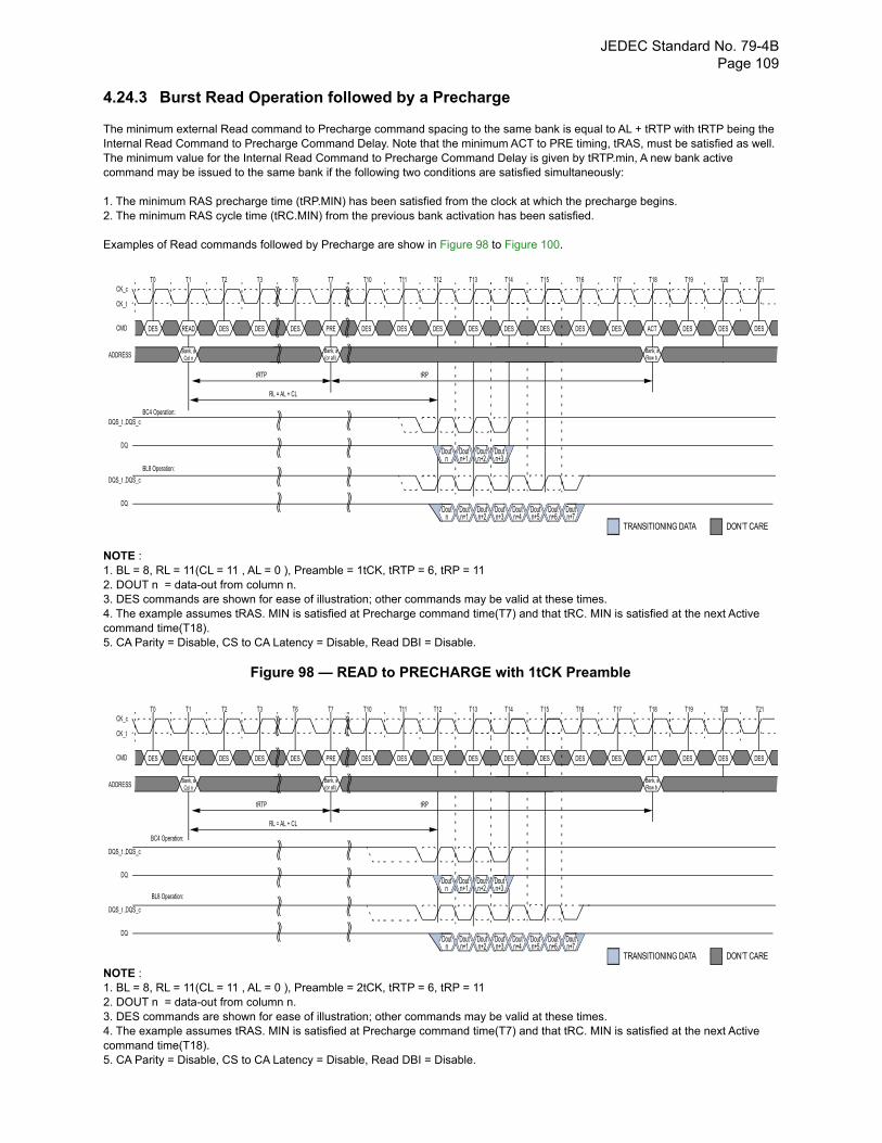
JEDEC Standard No. 79-4B Page 109
4.24.3 Burst Read Operation followed by a Precharge
The minimum external Read command to Precharge command spacing to the same bank is equal to AL + tRTP with tRTP being the Internal Read Command to Precharge Command Delay. Note that the minimum ACT to PRE timing, tRAS, must be satisfied as well. The minimum value for the Internal Read Command to Precharge Command Delay is given by tRTP.min, A new bank active command may be issued to the same bank if the following two conditions are satisfied simultaneously:
1. The minimum RAS precharge time (tRP.MIN) has been satisfied from the clock at which the precharge begins.2. The minimum RAS cycle time (tRC.MIN) from the previous bank activation has been satisfied.
Examples of Read commands followed by Precharge are show in Figure 98 to Figure 100.
NOTE :1. BL = 8, RL = 11(CL = 11 , AL = 0 ), Preamble = 1tCK, tRTP = 6, tRP = 112. DOUT n = data-out from column n.3. DES commands are shown for ease of illustration; other commands may be valid at these times.4. The example assumes tRAS. MIN is satisfied at Precharge command time(T7) and that tRC. MIN is satisfied at the next Active command time(T18).5. CA Parity = Disable, CS to CA Latency = Disable, Read DBI = Disable.
Figure 98 — READ to PRECHARGE with 1tCK Preamble
NOTE :1. BL = 8, RL = 11(CL = 11 , AL = 0 ), Preamble = 2tCK, tRTP = 6, tRP = 112. DOUT n = data-out from column n.3. DES commands are shown for ease of illustration; other commands may be valid at these times.4. The example assumes tRAS. MIN is satisfied at Precharge command time(T7) and that tRC. MIN is satisfied at the next Active command time(T18).5. CA Parity = Disable, CS to CA Latency = Disable, Read DBI = Disable.
DES
CK_c
CK_t
CMD
DQS_t ,DQS_c
DQ
T0 T1 T3 T6 T7 T10T2 T11 T12 T13 T14
READ DES DES DES PRE DES DES DES DES DES
Bank, aADDRESS
T15 T16
DES DES
Doutn
Doutn+2
Doutn+3
Doutn+1
Doutn+4
Doutn+5
Doutn+6
Doutn+7
DON’T CARETRANSITIONING DATA
T17 T18 T20 T21T19
DES ACT DES DES DES
Bank, a
Doutn
Doutn+2
Doutn+3
Doutn+1
(or all) Bank, aRow b Col n
tRTP tRP
RL = AL + CL
BC4 Operation:
DQS_t ,DQS_c
DQ
BL8 Operation:
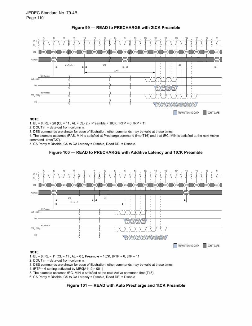
JEDEC Standard No. 79-4BPage 110
Figure 99 — READ to PRECHARGE with 2tCK Preamble
NOTE :1. BL = 8, RL = 20 (CL = 11 , AL = CL- 2 ), Preamble = 1tCK, tRTP = 6, tRP = 112. DOUT n = data-out from column n.3. DES commands are shown for ease of illustration; other commands may be valid at these times.4. The example assumes tRAS. MIN is satisfied at Precharge command time(T16) and that tRC. MIN is satisfied at the next Active command time(T27).5. CA Parity = Disable, CS to CA Latency = Disable, Read DBI = Disable.
Figure 100 — READ to PRECHARGE with Additive Latency and 1tCK Preamble
NOTE :1. BL = 8, RL = 11 (CL = 11 , AL = 0 ), Preamble = 1tCK, tRTP = 6, tRP = 112. DOUT n = data-out from column n.3. DES commands are shown for ease of illustration; other commands may be valid at these times.4. tRTP = 6 setting activated by MR0[A11:9 = 001]5. The example assumes tRC. MIN is satisfied at the next Active command time(T18).6. CA Parity = Disable, CS to CA Latency = Disable, Read DBI = Disable.
Figure 101 — READ with Auto Precharge and 1tCK Preamble
DES
CK_c
CK_t
CMD
DQS_t ,DQS_c
DQ
T0 T1 T3 T10 T11 T12T2 T13 T16 T19 T20
READ DES DES DES DES DES DES PRE DES DES
Bank, aADDRESS
T21 T22
DES DES
Doutn
Doutn+2
Doutn+3
Doutn+1
Doutn+4
Doutn+5
Doutn+6
Doutn+7
DON’T CARETRANSITIONING DATA
T23 T24 T26 T27T25
DES DES DES DES ACT
Bank, a
Doutn
Doutn+2
Doutn+3
Doutn+1
(or all) Bank, aRow b Col n
AL = CL - 2 = 9 tRTP
CL = 11
BC4 Operation:
DQS_t ,DQS_c
DQ
BL8 Operation:
tRP
DES
CK_c
CK_t
CMD
DQS_t ,DQS_c
DQ
T0 T1 T3 T6 T7 T10T2 T11 T12 T13 T14
RDA DES DES DES DES DES DES DES DES DES
Bank, aADDRESS
T15 T16
DES DES
Doutn
Doutn+2
Doutn+3
Doutn+1
Doutn+4
Doutn+5
Doutn+6
Doutn+7
DON’T CARETRANSITIONING DATA
T17 T18 T20 T21T19
DES ACT DES DES DES
Doutn
Doutn+2
Doutn+3
Doutn+1
Bank, aRow b Col n
tRTP
RL = AL + CL
BC4 Operation:
DQS_t ,DQS_c
DQ
BL8 Operation:
tRP
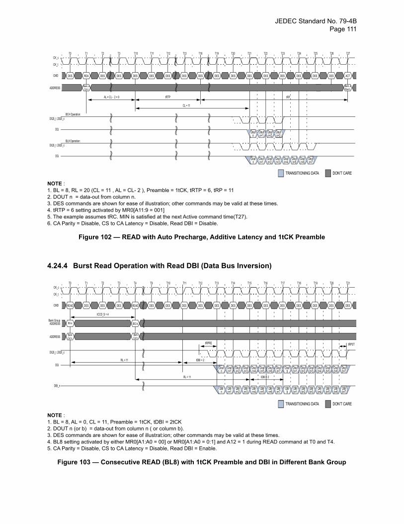
JEDEC Standard No. 79-4B Page 111
NOTE :1. BL = 8, RL = 20 (CL = 11 , AL = CL- 2 ), Preamble = 1tCK, tRTP = 6, tRP = 112. DOUT n = data-out from column n.3. DES commands are shown for ease of illustration; other commands may be valid at these times.4. tRTP = 6 setting activated by MR0[A11:9 = 001]5. The example assumes tRC. MIN is satisfied at the next Active command time(T27).6. CA Parity = Disable, CS to CA Latency = Disable, Read DBI = Disable.
Figure 102 — READ with Auto Precharge, Additive Latency and 1tCK Preamble
4.24.4 Burst Read Operation with Read DBI (Data Bus Inversion)
NOTE :1. BL = 8, AL = 0, CL = 11, Preamble = 1tCK, tDBI = 2tCK2. DOUT n (or b) = data-out from column n ( or column b).3. DES commands are shown for ease of illustrat:ion; other commands may be valid at these times.4. BL8 setting activated by either MR0[A1:A0 = 00] or MR0[A1:A0 = 0:1] and A12 = 1 during READ command at T0 and T4.5. CA Parity = Disable, CS to CA Latency = Disable, Read DBI = Enable.
Figure 103 — Consecutive READ (BL8) with 1tCK Preamble and DBI in Different Bank Group
DES
CK_c
CK_t
CMD
DQS_t ,DQS_c
DQ
T0 T1 T3 T10 T11 T12T2 T13 T16 T19 T20
RDA DES DES DES DES DES DES DES DES DES
Bank, aADDRESS
T21 T22
DES DES
Doutn
Doutn+2
Doutn+3
Doutn+1
Doutn+4
Doutn+5
Doutn+6
Doutn+7
DON’T CARETRANSITIONING DATA
T23 T24 T26 T27T25
DES DES DES DES ACT
Doutn
Doutn+2
Doutn+3
Doutn+1
Bank, aRow b Col n
AL = CL - 2 = 9 tRTP
CL = 11
BC4 Operation:
DQS_t ,DQS_c
DQ
BL8 Operation:
tRP
Doutn
Doutn+2
Doutn+3
Doutn+1
Doutn+4
Doutn+5
Doutn+6
Doutn+7
READ
CK_c
CK_t
CMD
DQS_t ,DQS_c
DQ
T0 T1 T3 T4 T9 T10T2 T11 T12 T13 T14
DES DES DES READ DES DES DES DES DES DES
BG aADDRESS
tRPRE tRPST
RL = 11
T15 T16
DES DES
Bank Group
BankADDRESS Col n
DON’T CARETRANSITIONING DATA
T17 T18 T20 T21T19
DES DES DES DES DES
BG b
BankCol b
RL = 11
tCCD_S = 4
Doutb
Doutb+2
Doutb+3
Doutb+1
Doutb+4
Doutb+5
Doutb+6
Doutb+7
tDBI = 2
tDBI = 2
DBIn
DBIn+2
DBIn+3
DBIn+1
DBIn+4
DBIn+5
DBIn+6
DBIn+7
DBI_nDBIb
DBIb+2
DBIb+3
DBIb+1
DBIb+4
DBIb+5
DBIb+6
DBIb+7
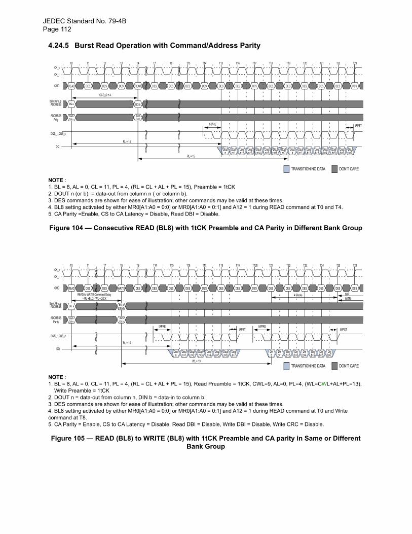
JEDEC Standard No. 79-4BPage 112
4.24.5 Burst Read Operation with Command/Address Parity
NOTE :1. BL = 8, AL = 0, CL = 11, PL = 4, (RL = CL + AL + PL = 15), Preamble = 1tCK2. DOUT n (or b) = data-out from column n ( or column b).3. DES commands are shown for ease of illustration; other commands may be valid at these times.4. BL8 setting activated by either MR0[A1:A0 = 0:0] or MR0[A1:A0 = 0:1] and A12 = 1 during READ command at T0 and T4.5. CA Parity =Enable, CS to CA Latency = Disable, Read DBI = Disable.
Figure 104 — Consecutive READ (BL8) with 1tCK Preamble and CA Parity in Different Bank Group
NOTE :1. BL = 8, AL = 0, CL = 11, PL = 4, (RL = CL + AL + PL = 15), Read Preamble = 1tCK, CWL=9, AL=0, PL=4, (WL=CWL+AL+PL=13), Write Preamble = 1tCK2. DOUT n = data-out from column n, DIN b = data-in to column b.3. DES commands are shown for ease of illustration; other commands may be valid at these times.4. BL8 setting activated by either MR0[A1:A0 = 0:0] or MR0[A1:A0 = 0:1] and A12 = 1 during READ command at T0 and Write command at T8.5. CA Parity = Enable, CS to CA Latency = Disable, Read DBI = Disable, Write DBI = Disable, Write CRC = Disable.
Figure 105 — READ (BL8) to WRITE (BL8) with 1tCK Preamble and CA parity in Same or Different Bank Group
Doutn
Doutn+2
Doutn+3
Doutn+1
Doutn+4
Doutn+5
Doutn+6
Doutn+7
READ
CK_c
CK_t
CMD
DQS_t ,DQS_c
DQ
T0 T1 T3 T4 T7 T8T2 T13 T14 T15 T16
DES DES DES READ DES DES DES DES DES DES
BG aADDRESS
tRPRE tRPST
RL = 15
T17 T18
DES DES
Bank Group
BankADDRESSCol n
DON’T CARETRANSITIONING DATA
T19 T20 T22 T23T21
DES DES DES DES DES
BG b
BankCol b
RL = 15
tCCD_S = 4
Doutb
Doutb+2
Doutb+3
Doutb+1
Doutb+4
Doutb+5
Doutb+6
Doutb+7
Prity
READ
CK_c
CK_t
CMD
DQS_t ,DQS_c
DQ
T0 T1 T8 T9 T14 T15T7 T16 T17 T18 T19
DES DES WRITE DES DES DES DES DES DES DES
BG aADDRESS
tRPREtRPST
RL = 15
T120 T21
DES DES
Bank Group
BankADDRESSCol n
Doutn
Doutn+2
Doutn+3
Doutn+1
Doutn+4
Doutn+5
Doutn+6
Doutn+7
DON’T CARETRANSITIONING DATA
T22 T23 T25 T26T24
DES DES DES DES DES
BG a
BankCol b
WL = 13
READ to WRITE Command Delay
or BG b
= RL +BL/2 - WL + 2tCK
tWPREtWPST
4 Clocks tWRtWTR
Dinb
Dinb+2
Dinb+3
Dinb+1
Dinb+4
Dinb+5
Dinb+6
Dinb+7
Parity
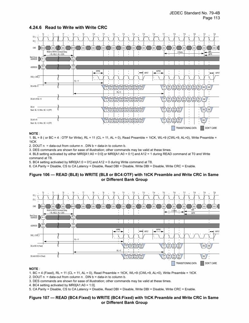
JEDEC Standard No. 79-4B Page 113
4.24.6 Read to Write with Write CRC
READ
CK_c
CK_t
CMD
DQS_t ,DQS_c
DQ x4 BL= 8
T0 T1 T8 T9 T10 T11T7 T12 T13 T14 T15
DES DES WRITE DES DES DES DES DES DES DES
BG aADDRESS
tRPREtRPST
RL = 11
T16 T17
DES DES
Bank Group
BankADDRESS Col n
Doutn
Doutn+2
Doutn+3
Doutn+1
Doutn+4
Doutn+5
Doutn+6
Doutn+7
DON’T CARETRANSITIONING DATA
T18 T19 T21 T22T20
DES DES DES DES DES
BG a
BankCol b
Dinb
Dinb+2 CRCDin
b+1
WL = 9
READ to WRITE Command Delay
or BG b
= RL +BL/2 - WL + 2tCK
tWPREtWPST
4 Clocks tWRtWTR
Dinb+4
Dinb+3
Dinb+6
Dinb+5 CRCDin
b+7
DQ x8/ x16 BL = 8 Doutn
Doutn+2
Doutn+3
Doutn+1
Doutn+4
Doutn+5
Doutn+6
Doutn+7
Dinb
Dinb+2 CRCDin
b+1Dinb+4
Dinb+3
Dinb+6
Dinb+5
Dinb+7
DQ x4Dout
nDoutn+2
Doutn+3
Doutn+1
Doutn+4
Doutn+5
Doutn+6
Doutn+7
Dinb
Dinb+2 CRCDin
b+1Dinb+3 CRC
DQ x8/ x16 Doutn
Doutn+2
Doutn+3
Doutn+1
Doutn+4
Doutn+5
Doutn+6
Doutn+7
Dinb
Dinb+2
Dinb+1
Dinb+3 CRC
Read : BL = 8, Write : BC = 4 (OTF)
Read : BL = 8, Write : BC = 4 (OTF)
NOTE :1. BL = 8 ( or BC = 4 : OTF for Write), RL = 11 (CL = 11, AL = 0), Read Preamble = 1tCK, WL=9 (CWL=9, AL=0), Write Preamble = 1tCK2. DOUT n = data-out from column n . DIN b = data-in to column b.3. DES commands are shown for ease of illustration; other commands may be valid at these times.4. BL8 setting activated by either MR0[A1:A0 = 0:0] or MR0[A1:A0 = 0:1] and A12 = 1 during READ command at T0 and Write command at T8.5. BC4 setting activated by MR0[A1:0 = 01] and A12 = 0 during Write command at T8.6. CA Parity = Disable, CS to CA Latency = Disable, Read DBI = Disable, Write DBI = Disable, Write CRC = Enable.
Figure 106 — READ (BL8) to WRITE (BL8 or BC4:OTF) with 1tCK Preamble and Write CRC in Same or Different Bank Group
NOTE :1. BC = 4 (Fixed), RL = 11 (CL = 11, AL = 0), Read Preamble = 1tCK, WL=9 (CWL=9, AL=0), Write Preamble = 1tCK2. DOUT n = data-out from column n . DIN b = data-in to column b.3. DES commands are shown for ease of illustration; other commands may be valid at these times.4. BC4 setting activated by MR0[A1:A0 = 1:0].5. CA Parity = Disable, CS to CA Latency = Disable, Read DBI = Disable, Write DBI = Disable, Write CRC = Enable.
Figure 107 — READ (BC4:Fixed) to WRITE (BC4:Fixed) with 1tCK Preamble and Write CRC in Same or Different Bank Group
READ
CK_c
CK_t
CMD
DQS_t ,DQS_c
DQ x4 BC=4 (Fixed)
T0 T1 T6 T7 T8 T9T5 T10 T11 T12 T13
DES DES WRITE DES DES DES DES DES DES DES
BG aADDRESS
tRPREtRPST
RL = 11
T14 T15
DES DES
Bank Group
BankADDRESS Col n
DON’T CARETRANSITIONING DATA
T16 T17 T19 T20T18
DES DES DES DES DES
BG a
BankCol b
WL = 9
READ to WRITE Command Delay
or BG b
= RL +BC/2 - WL + 2tCK
tWPREtWPST
2 Clocks tWR
tWTR
Doutn
Doutn+2
Doutn+3
Doutn+1
Dinb
Dinb+2
Dinb+3
Dinb+1 CRCCRC
Doutn
Doutn+2
Doutn+3
Doutn+1
Dinb
Dinb+2
Dinb+3
Dinb+1 CRCDQ x8/x16 BC=4 (Fixed)
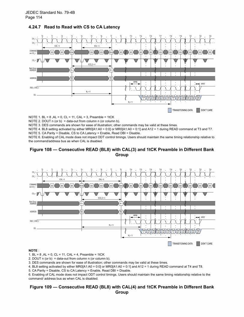
JEDEC Standard No. 79-4BPage 114
4.24.7 Read to Read with CS to CA Latency
NOTE 1. BL = 8 ,AL = 0, CL = 11, CAL = 3, Preamble = 1tCKNOTE 2. DOUT n (or b) = data-out from column n (or column b).NOTE 3. DES commands are shown for ease of illustration; other commands may be valid at these times.NOTE 4. BL8 setting activated by either MR0[A1:A0 = 0:0] or MR0[A1:A0 = 0:1] and A12 = 1 during READ command at T3 and T7.NOTE 5. CA Parity = Disable, CS to CA Latency = Enable, Read DBI = Disable.NOTE 6. Enabling of CAL mode does not impact ODT control timings. Users should maintain the same timing relationship relative to the command/address bus as when CAL is disabled.
Figure 108 — Consecutive READ (BL8) with CAL(3) and 1tCK Preamble in Different Bank Group
NOTE :1. BL = 8 ,AL = 0, CL = 11, CAL = 4, Preamble = 1tCK2. DOUT n (or b) = data-out from column n (or column b).3. DES commands are shown for ease of illustration; other commands may be valid at these times.4. BL8 setting activated by either MR0[A1:A0 = 0:0] or MR0[A1:A0 = 0:1] and A12 = 1 during READ command at T4 and T8.5. CA Parity = Disable, CS to CA Latency = Enable, Read DBI = Disable.6. Enabling of CAL mode does not impact ODT control timings. Users should maintain the same timing relationship relative to the command/ address bus as when CAL is disabled.
Figure 109 — Consecutive READ (BL8) with CAL(4) and 1tCK Preamble in Different Bank Group
CK_c
CK_t
DQS_t ,DQS_c
DQ
T0 T1 T3 T4 T5 T6T2 T7 T8 T13 T14
DES DES READ DES DES READ DES DES DES
ADDRESS
tRPRE
RL = 11
T15 T17
DES DES
Bank Group
ADDRESS
DON’T CARETRANSITIONING DATA
T18 T19 T22 T23T21
DES DES DES DES DES
BG a
tRPST
tCAL = 3 tCAL = 3
tCCD_S = 4
BG b
Bank, Bank,Col n Col b
Doutn
Doutn+2
Doutn+5
Doutn+1
Doutn+6
Doutn+7
Doutb
Doutb+1
Doutb+2
Doutb+6
Doutb+7
Doutb+5
RL = 11
COMMANDw/o CS_n
CS_n
CK_c
CK_t
DQS_t ,DQS_c
DQ
T0 T1 T3 T4 T5 T6T2 T7 T8 T14 T15
DES DES DES DES DES DES READ DES DES
ADDRESS
tRPRE
RL = 11
T16 T18
DES DES
Bank Group
ADDRESS
DON’T CARETRANSITIONING DATA
T19 T20 T23 T24T22
DES DES DES DES DES
BG a
tRPST
tCAL = 4 tCAL = 4
tCCD_S = 4
BG b
Bank, Bank,Col n Col b
Doutn
Doutn+2
Doutn+5
Doutn+1
Doutn+6
Doutn+7
Doutb
Doutb+1
Doutb+2
Doutb+6
Doutb+7
Doutb+5
RL = 11
COMMANDw/o CS_n READ
CS_n
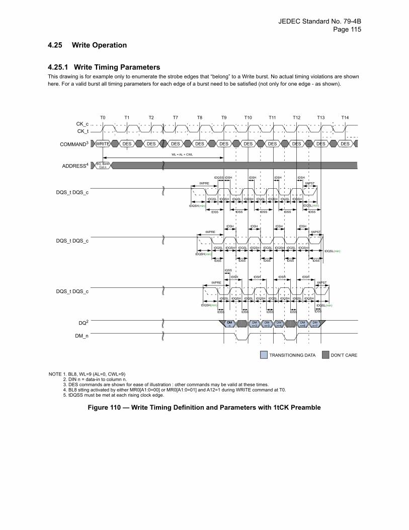
JEDEC Standard No. 79-4B Page 115
4.25 Write Operation
4.25.1 Write Timing ParametersThis drawing is for example only to enumerate the strobe edges that “belong” to a Write burst. No actual timing violations are shown here. For a valid burst all timing parameters for each edge of a burst need to be satisfied (not only for one edge - as shown).
Figure 110 — Write Timing Definition and Parameters with 1tCK Preamble
DON’T CARETRANSITIONING DATA
DESWRITE DES DES DES DES DES DES DES DES DES
T0 T1 T2 T7 T8 T9 T10 T11 T12 T13 T14
BG, BankCol n
CK_c
CK_t
COMMAND3
ADDRESS4
WL = AL + CWL
tWPRE
tDQSL tDQSH
tDSS tDSS
tDQSS tDSH
tDQSL tDQSH tDQSL tDQSH tDQSL tDQSH
tDSS tDSS tDSS
tDSH tDSH tDSH
tDQSL(min)
tWPST
tDQSH(min)
tWPRE
tDQSL tDQSH
tDSS tDSS
tDSH
tDQSL tDQSH tDQSL tDQSH tDQSL tDQSH
tDSS tDSS tDSS
tDSH tDSH tDSH
tWPST
tWPRE
tDQSL tDQSH
tDSS tDSS
tDSH
tDQSL tDQSH tDQSL tDQSH tDQSL tDQSH
tDSS tDSS tDSS
tDSH tDSH tDSH
tWPST
tQSS
DQS_t DQS_c
DQS_t DQS_c
DQS_t DQS_c
DQ2 DM DMn+2
DMn+3
DMn+4
DMn
DMn+6
DMn+7
DM_n
NOTE 1. BL8, WL=9 (AL=0, CWL=9)2. DIN n = data-in to column n.3. DES commands are shown for ease of illustration : other commands may be valid at these times.4. BL8 stting activated by either MR0[A1:0=00] or MR0[A1:0=01] and A12=1 during WRITE command at T0.5. tDQSS must be met at each rising clock edge.
tDQSH(min)
tDQSH(min)
tDQSL(min)
tDQSL(min)
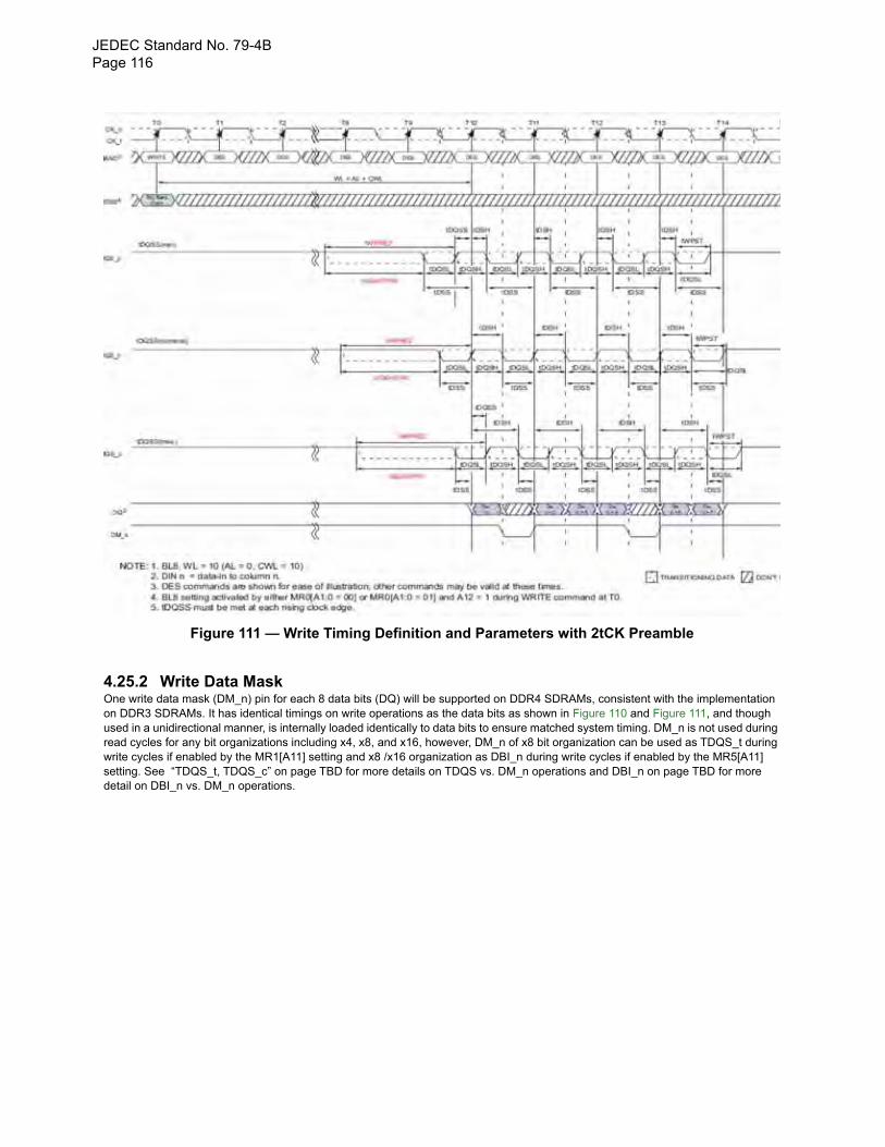
JEDEC Standard No. 79-4BPage 116
Figure 111 — Write Timing Definition and Parameters with 2tCK Preamble
4.25.2 Write Data MaskOne write data mask (DM_n) pin for each 8 data bits (DQ) will be supported on DDR4 SDRAMs, consistent with the implementation on DDR3 SDRAMs. It has identical timings on write operations as the data bits as shown in Figure 110 and Figure 111, and though used in a unidirectional manner, is internally loaded identically to data bits to ensure matched system timing. DM_n is not used during read cycles for any bit organizations including x4, x8, and x16, however, DM_n of x8 bit organization can be used as TDQS_t during write cycles if enabled by the MR1[A11] setting and x8 /x16 organization as DBI_n during write cycles if enabled by the MR5[A11] setting. See “TDQS_t, TDQS_c” on page TBD for more details on TDQS vs. DM_n operations and DBI_n on page TBD for more detail on DBI_n vs. DM_n operations.
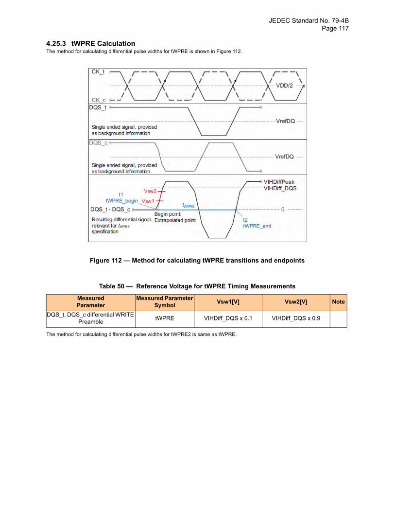
JEDEC Standard No. 79-4B Page 117
4.25.3 tWPRE CalculationThe method for calculating differential pulse widths for tWPRE is shown in Figure 112.
Figure 112 — Method for calculating tWPRE transitions and endpoints
Table 50 — Reference Voltage for tWPRE Timing Measurements
The method for calculating differential pulse widths for tWPRE2 is same as tWPRE.
MeasuredParameter
Measured Parameter Symbol
Vsw1[V] Vsw2[V] Note
DQS_t, DQS_c differential WRITE Preamble
tWPRE VIHDiff_DQS x 0.1 VIHDiff_DQS x 0.9
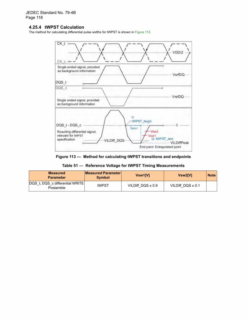
JEDEC Standard No. 79-4BPage 118
4.25.4 tWPST CalculationThe method for calculating differential pulse widths for tWPST is shown in Figure 113.
Figure 113 — Method for calculating tWPST transitions and endpoints
Table 51 — Reference Voltage for tWPST Timing Measurements
MeasuredParameter
Measured Parameter Symbol
Vsw1[V] Vsw2[V] Note
DQS_t, DQS_c differential WRITE Postamble
tWPST VILDiff_DQS x 0.9 VILDiff_DQS x 0.1
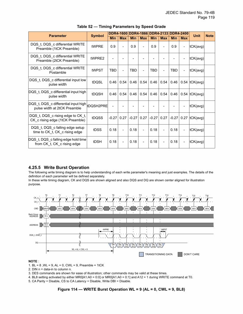
JEDEC Standard No. 79-4B Page 119
Table 52 — Timing Parameters by Speed Grade
4.25.5 Write Burst OperationThe following write timing diagram is to help understanding of each write parameter's meaning and just examples. The details of the definition of each parameter will be defined separately.In these write timing diagram, CK and DQS are shown aligned and also DQS and DQ are shown center aligned for illustration purpose.
NOTE :1. BL = 8 ,WL = 9, AL = 0, CWL = 9, Preamble = 1tCK2. DIN n = data-in to column n.3. DES commands are shown for ease of illustration; other commands may be valid at these times.4. BL8 setting activated by either MR0[A1:A0 = 0:0] or MR0[A1:A0 = 0:1] and A12 = 1 during WRITE command at T0.5. CA Parity = Disable, CS to CA Latency = Disable, Write DBI = Disable.
Figure 114 — WRITE Burst Operation WL = 9 (AL = 0, CWL = 9, BL8)
Parameter SymbolDDR4-1600 DDR4-1866 DDR4-2133 DDR4-2400
Unit NoteMin Max Min Max Min Max Min Max
DQS_t, DQS_c differential WRITE Preamble (1tCK Preamble)
tWPRE 0.9 - 0.9 - 0.9 - 0.9 - tCK(avg)
DQS_t, DQS_c differential WRITE Preamble (2tCK Preamble)
tWPRE2 - - - - - - - - tCK(avg)
DQS_t, DQS_c differential WRITE Postamble
tWPST TBD - TBD - TBD - TBD - tCK(avg)
DQS_t, DQS_c differential input low pulse width
tDQSL 0.46 0.54 0.46 0.54 0.46 0.54 0.46 0.54 tCK(avg)
DQS_t, DQS_c differential input high pulse width
tDQSH 0.46 0.54 0.46 0.54 0.46 0.54 0.46 0.54 tCK(avg)
DQS_t, DQS_c differential input high pulse width at 2tCK Preamble
tDQSH2PRE - - - - - - - - tCK(avg)
DQS_t, DQS_c rising edge to CK_t, CK_c rising edge (1tCK Preamble)
tDQSS -0.27 0.27 -0.27 0.27 -0.27 0.27 -0.27 0.27 tCK(avg)
DQS_t, DQS_c falling edge setup time to CK_t, CK_c rising edge
tDSS 0.18 - 0.18 - 0.18 - 0.18 - tCK(avg)
DQS_t, DQS_c falling edge hold time from CK_t, CK_c rising edge
tDSH 0.18 - 0.18 - 0.18 - 0.18 - tCK(avg)
WRITE
CK_c
CK_t
CMD
DQS_t ,DQS_c
DQ
T0 T1 T7 T8 T9 T10T2 T11 T12 T13 T14
DES DES DES DES DES DES DES DES DES DES
BG aADDRESS
tWPRE tWPST
WL = AL + CWL = 9
T15 T16
DES DES
Bank Group
Bank,ADDRESS Col n
Dinn
Dinn+2
Dinn+3
Dinn+1
Dinn+4
Dinn+5
Dinn+6
Dinn+7
DON’T CARETRANSITIONING DATA
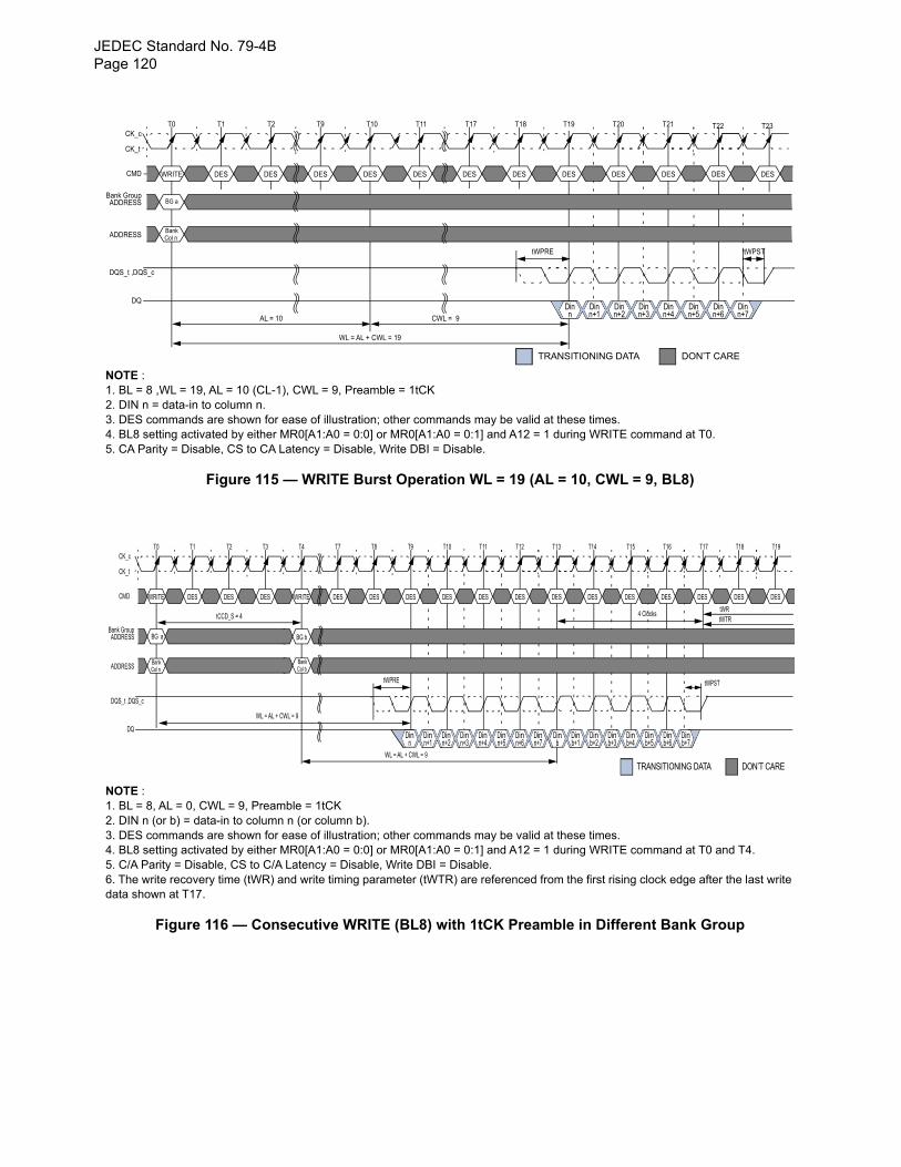
JEDEC Standard No. 79-4BPage 120
NOTE :1. BL = 8 ,WL = 19, AL = 10 (CL-1), CWL = 9, Preamble = 1tCK2. DIN n = data-in to column n.3. DES commands are shown for ease of illustration; other commands may be valid at these times.4. BL8 setting activated by either MR0[A1:A0 = 0:0] or MR0[A1:A0 = 0:1] and A12 = 1 during WRITE command at T0.5. CA Parity = Disable, CS to CA Latency = Disable, Write DBI = Disable.
Figure 115 — WRITE Burst Operation WL = 19 (AL = 10, CWL = 9, BL8)
NOTE :1. BL = 8, AL = 0, CWL = 9, Preamble = 1tCK 2. DIN n (or b) = data-in to column n (or column b).3. DES commands are shown for ease of illustration; other commands may be valid at these times.4. BL8 setting activated by either MR0[A1:A0 = 0:0] or MR0[A1:A0 = 0:1] and A12 = 1 during WRITE command at T0 and T4.5. C/A Parity = Disable, CS to C/A Latency = Disable, Write DBI = Disable.6. The write recovery time (tWR) and write timing parameter (tWTR) are referenced from the first rising clock edge after the last write data shown at T17.
Figure 116 — Consecutive WRITE (BL8) with 1tCK Preamble in Different Bank Group
WRITE
CK_c
CK_t
CMD
DQS_t ,DQS_c
DQ
T0 T1 T9 T10 T11 T17T2 T18 T19 T20 T21
DES DES DES DES DES DES DES DES DES DES
BG aADDRESS
tWPRE tWPST
CWL = 9
WL = AL + CWL = 19
T22 T23
DES DES
Bank Group
BankADDRESS Col n
Dinn
Dinn+2
Dinn+3
Dinn+1
Dinn+4
Dinn+5
Dinn+6
Dinn+7
DON’T CARETRANSITIONING DATA
AL = 10
WRITE
CK_c
CK_t
CMD
DQS_t ,DQS_c
DQ
T0 T1 T3 T4 T7 T8T2 T9 T10 T11 T12
DES DES DES WRITE DES DES DES DES DES DES
BG aADDRESS
tWPRE tWPST
WL = AL + CWL = 9
T13 T14
DES DES
Bank Group
BankADDRESS Col n
Dinn
Dinn+2
Dinn+3
Dinn+1
Dinn+4
Dinn+5
Dinn+6
Dinn+7
DON’T CARETRANSITIONING DATA
T15 T16 T18 T19T17
DES DES DES DES DES
BG b
BankCol b
Dinb
Dinb+2
Dinb+3
Dinb+1
Dinb+4
Dinb+5
Dinb+6
Dinb+7
tCCD_S = 4 4 ClockstWRtWTR
WL = AL + CWL = 9
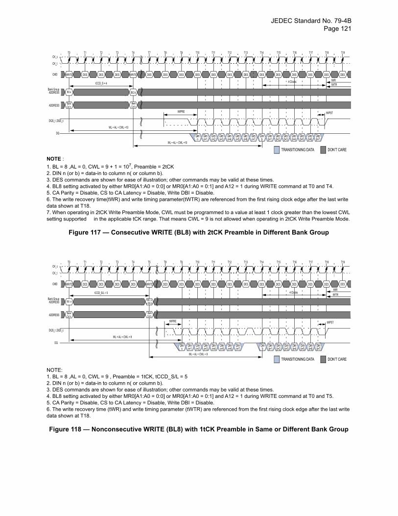
JEDEC Standard No. 79-4B Page 121
NOTE :
1. BL = 8 ,AL = 0, CWL = 9 + 1 = 107, Preamble = 2tCK2. DIN n (or b) = data-in to column n( or column b).3. DES commands are shown for ease of illustration; other commands may be valid at these times.4. BL8 setting activated by either MR0[A1:A0 = 0:0] or MR0[A1:A0 = 0:1] and A12 = 1 during WRITE command at T0 and T4.5. CA Parity = Disable, CS to CA Latency = Disable, Write DBI = Disable.6. The write recovery time(tWR) and write timing parameter(tWTR) are referenced from the first rising clock edge after the last write data shown at T18.7. When operating in 2tCK Write Preamble Mode, CWL must be programmed to a value at least 1 clock greater than the lowest CWL setting supported in the applicable tCK range. That means CWL = 9 is not allowed when operating in 2tCK Write Preamble Mode.
Figure 117 — Consecutive WRITE (BL8) with 2tCK Preamble in Different Bank Group
NOTE:1. BL = 8 ,AL = 0, CWL = 9 , Preamble = 1tCK, tCCD_S/L = 52. DIN n (or b) = data-in to column n( or column b).3. DES commands are shown for ease of illustration; other commands may be valid at these times.4. BL8 setting activated by either MR0[A1:A0 = 0:0] or MR0[A1:A0 = 0:1] and A12 = 1 during WRITE command at T0 and T5.5. CA Parity = Disable, CS to CA Latency = Disable, Write DBI = Disable.6. The write recovery time (tWR) and write timing parameter (tWTR) are referenced from the first rising clock edge after the last write data shown at T18.
Figure 118 — Nonconsecutive WRITE (BL8) with 1tCK Preamble in Same or Different Bank Group
WRITE
CK_c
CK_t
CMD
DQS_t ,DQS_c
DQ
T0 T1 T3 T4 T7 T8T2 T9 T10 T11 T12
DES DES DES WRITE DES DES DES DES DES DES
BG aADDRESS
tWPRE tWPST
WL = AL + CWL =10
T13 T14
DES DES
Bank Group
BankADDRESS Col n
Dinn
Dinn+2
Dinn+3
Dinn+1
Dinn+4
Dinn+5
Dinn+6
Dinn+7
DON’T CARETRANSITIONING DATA
T15 T16 T18 T19T17
DES DES DES DES DES
BG b
BankCol b
Dinb
Dinb+2
Dinb+3
Dinb+1
Dinb+4
Dinb+5
Dinb+6
Dinb+7
tCCD_S = 4 4 ClockstWTRtWR
WL = AL + CWL =10
WRITE
CK_c
CK_t
CMD
DQS_t ,DQS_c
DQ
T0 T1 T3 T4 T5 T8T2 T9 T10 T11 T12
DES DES DES DES WRITE DES DES DES DES DES
BG aADDRESS
tWPRE tWPST
WL = AL + CWL = 9
T13 T14
DES DES
Bank Group
BankADDRESS Col n
Dinn
Dinn+2
Dinn+3
Dinn+1
Dinn+4
Dinn+5
Dinn+6
Dinn+7
DON’T CARETRANSITIONING DATA
T15 T16 T18 T19T17
DES DES DES DES DES
BG a
BankCol b
Dinb
Dinb+2
Dinb+3
Dinb+1
Dinb+4
Dinb+5
Dinb+6
Dinb+7
tCCD_S/L = 5
or BG b
4 ClockstWR
tWTR
WL = AL + CWL = 9
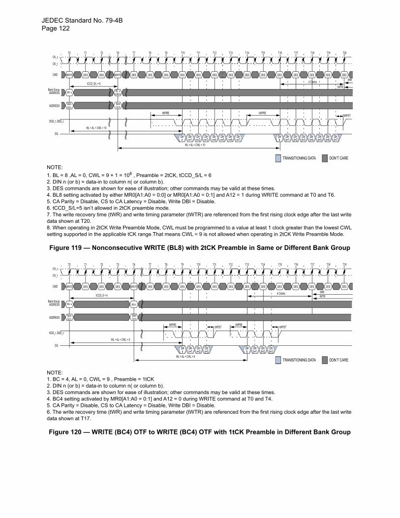
JEDEC Standard No. 79-4BPage 122
NOTE:
1. BL = 8 ,AL = 0, CWL = 9 + 1 = 108 , Preamble = 2tCK, tCCD_S/L = 62. DIN n (or b) = data-in to column n( or column b).3. DES commands are shown for ease of illustration; other commands may be valid at these times.4. BL8 setting activated by either MR0[A1:A0 = 0:0] or MR0[A1:A0 = 0:1] and A12 = 1 during WRITE command at T0 and T6.5. CA Parity = Disable, CS to CA Latency = Disable, Write DBI = Disable.6. tCCD_S/L=5 isn’t allowed in 2tCK preamble mode.7. The write recovery time (tWR) and write timing parameter (tWTR) are referenced from the first rising clock edge after the last write data shown at T20.8. When operating in 2tCK Write Preamble Mode, CWL must be programmed to a value at least 1 clock greater than the lowest CWL setting supported in the applicable tCK range.That means CWL = 9 is not allowed when operating in 2tCK Write Preamble Mode.
Figure 119 — Nonconsecutive WRITE (BL8) with 2tCK Preamble in Same or Different Bank Group
NOTE:1. BC = 4, AL = 0, CWL = 9 , Preamble = 1tCK2. DIN n (or b) = data-in to column n( or column b).3. DES commands are shown for ease of illustration; other commands may be valid at these times.4. BC4 setting activated by MR0[A1:A0 = 0:1] and A12 = 0 during WRITE command at T0 and T4.5. CA Parity = Disable, CS to CA Latency = Disable, Write DBI = Disable.6. The write recovery time (tWR) and write timing parameter (tWTR) are referenced from the first rising clock edge after the last write data shown at T17.
Figure 120 — WRITE (BC4) OTF to WRITE (BC4) OTF with 1tCK Preamble in Different Bank Group
WRITE
CK_c
CK_t
CMD
DQS_t ,DQS_c
DQ
T0 T1 T6 T7 T8 T9T2 T10 T11 T12 T13
DES DES WRITE DES DES DES DES DES DES DES
BG aADDRESS
tWPREtWPST
WL = AL + CWL = 10
T14 T15
DES DES
Bank Group
BankADDRESS Col n
Dinn
Dinn+2
Dinn+3
Dinn+1
Dinn+4
Dinn+5
Dinn+6
Dinn+7
DON’T CARETRANSITIONING DATA
T16 T17 T19 T20T18
DES DES DES DES DES
Dinb
Dinb+2
Dinb+3
Dinb+1
Dinb+4
Dinb+5
Dinb+6
Dinb+7
tCCD_S/L = 6
tWPRE
4 Clocks
tWTR
tWR
BG aor BG b
BankCol b
WL = AL + CWL = 10
WRITE
CK_c
CK_t
CMD
DQS_t ,DQS_c
DQ
T0 T1 T3 T4 T7 T8T2 T9 T10 T11 T12
DES DES DES WRITE DES DES DES DES DES DES
BG aADDRESS
tWPREtWPST
WL = AL + CWL = 9
T13 T14
DES DES
Bank Group
BankADDRESS Col n
Dinn
Dinn+2
Dinn+3
Dinn+1
DON’T CARETRANSITIONING DATA
T15 T16 T18 T19T17
DES DES DES DES DES
BankCol b
tCCD_S = 4
BG b
tWPREtWPST
Dinb
Dinb+2
Dinb+3
Dinb+1
4 Clocks tWRtWTR
WL = AL + CWL = 9
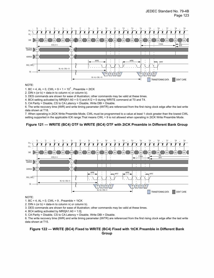
JEDEC Standard No. 79-4B Page 123
NOTE:
1. BC = 4, AL = 0, CWL = 9 + 1 = 107 , Preamble = 2tCK2. DIN n (or b) = data-in to column n( or column b).3. DES commands are shown for ease of illustration; other commands may be valid at these times.4. BC4 setting activated by MR0[A1:A0 = 0:1] and A12 = 0 during WRITE command at T0 and T4.5. CA Parity = Disable, CS to CA Latency = Disable, Write DBI = Disable.6. The write recovery time (tWR) and write timing parameter (tWTR) are referenced from the first rising clock edge after the last write data shown at T18.7. When operating in 2tCK Write Preamble Mode, CWL must be programmed to a value at least 1 clock greater than the lowest CWL setting supported in the applicable tCK range.That means CWL = 9 is not allowed when operating in 2tCK Write Preamble Mode.
Figure 121 — WRITE (BC4) OTF to WRITE (BC4) OTF with 2tCK Preamble in Different Bank Group
NOTE:1. BC = 4, AL = 0, CWL = 9 , Preamble = 1tCK2. DIN n (or b) = data-in to column n( or column b).3. DES commands are shown for ease of illustration; other commands may be valid at these times.4. BC4 setting activated by MR0[A1:A0 = 1:0].5. CA Parity = Disable, CS to CA Latency = Disable, Write DBI = Disable.6. The write recovery time (tWR) and write timing parameter (tWTR) are referenced from the first rising clock edge after the last write data shown at T15.
Figure 122 — WRITE (BC4) Fixed to WRITE (BC4) Fixed with 1tCK Preamble in Different Bank Group
WRITE
CK_c
CK_t
CMD
DQS_t ,DQS_c
DQ
T0 T1 T3 T4 T7 T8T2 T9 T10 T11 T12
DES DES DES WRITE DES DES DES DES DES DES
BG aADDRESS
tWPRE
WL = AL + CWL = 10
T13 T14
DES DES
Bank Group
BankADDRESS Col n
Dinn
Dinn+2
Dinn+3
Dinn+1
DON’T CARETRANSITIONING DATA
T15 T16 T18 T19T17
DES DES DES DES DES
BankCol b
tCCD_S = 4
BG b
tWPREtWPST
Dinb
Dinb+2
Dinb+3
Dinb+1
WL = AL + CWL = 10
4 ClockstWTRtWR
WRITE
CK_c
CK_t
CMD
DQS_t ,DQS_c
DQ
T0 T1 T3 T4 T7 T8T2 T9 T10 T11 T12
DES DES DES WRITE DES DES DES DES DES DES
BG aADDRESS
tWPRE
WL = AL + CWL = 9
T13 T14
DES DES
Bank Group
BankADDRESS Col n
Dinn
Dinn+2
Dinn+3
Dinn+1
DON’T CARETRANSITIONING DATA
T15 T16 T18 T19T17
DES DES DES DES DES
BankCol b
tCCD_S = 4
BG b
tWPREtWPST
Dinb
Dinb+2
Dinb+3
Dinb+1
tWPST
WL = AL + CWL = 9
tWRtWTR
2 Clocks
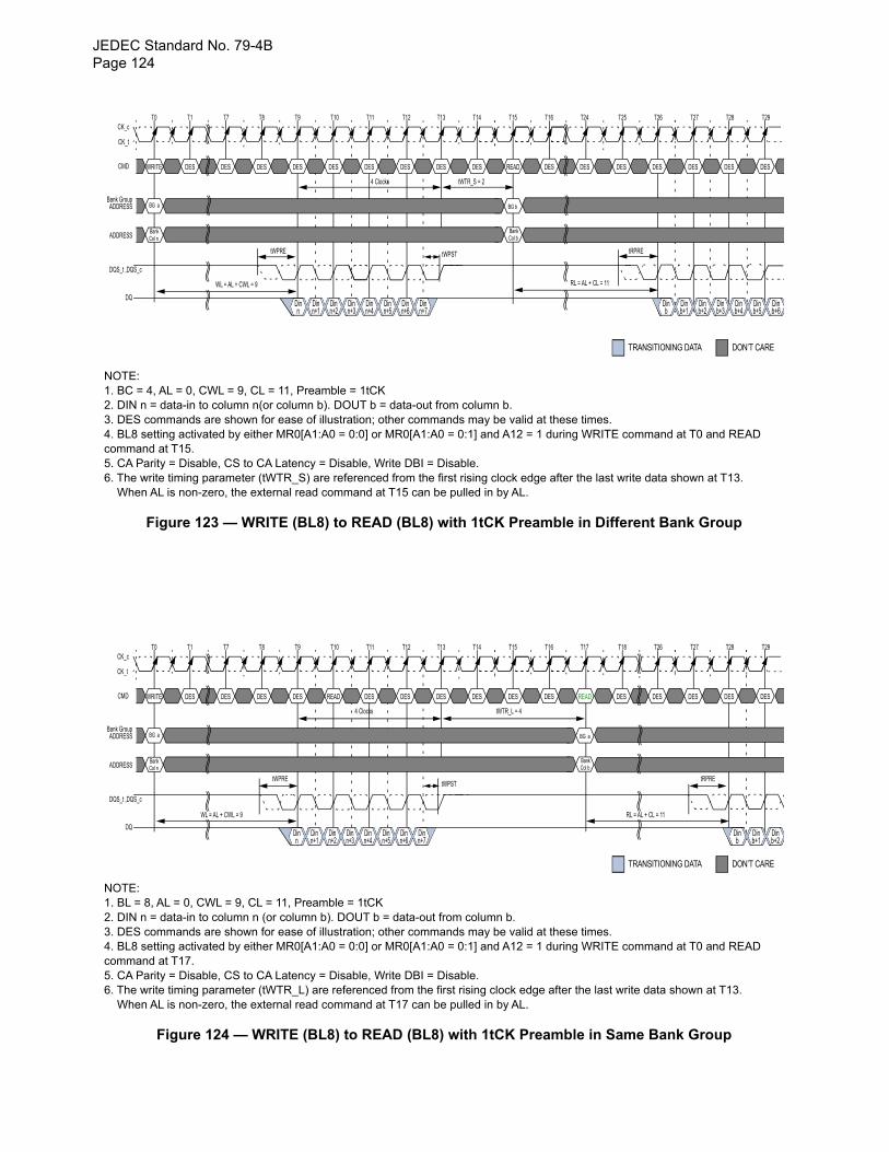
JEDEC Standard No. 79-4BPage 124
NOTE:1. BC = 4, AL = 0, CWL = 9, CL = 11, Preamble = 1tCK2. DIN n = data-in to column n(or column b). DOUT b = data-out from column b.3. DES commands are shown for ease of illustration; other commands may be valid at these times.4. BL8 setting activated by either MR0[A1:A0 = 0:0] or MR0[A1:A0 = 0:1] and A12 = 1 during WRITE command at T0 and READ command at T15.5. CA Parity = Disable, CS to CA Latency = Disable, Write DBI = Disable.6. The write timing parameter (tWTR_S) are referenced from the first rising clock edge after the last write data shown at T13. When AL is non-zero, the external read command at T15 can be pulled in by AL.
Figure 123 — WRITE (BL8) to READ (BL8) with 1tCK Preamble in Different Bank Group
NOTE:1. BL = 8, AL = 0, CWL = 9, CL = 11, Preamble = 1tCK2. DIN n = data-in to column n (or column b). DOUT b = data-out from column b.3. DES commands are shown for ease of illustration; other commands may be valid at these times.4. BL8 setting activated by either MR0[A1:A0 = 0:0] or MR0[A1:A0 = 0:1] and A12 = 1 during WRITE command at T0 and READ command at T17.5. CA Parity = Disable, CS to CA Latency = Disable, Write DBI = Disable.6. The write timing parameter (tWTR_L) are referenced from the first rising clock edge after the last write data shown at T13. When AL is non-zero, the external read command at T17 can be pulled in by AL.
Figure 124 — WRITE (BL8) to READ (BL8) with 1tCK Preamble in Same Bank Group
WRITE
CK_c
CK_t
CMD
DQS_t ,DQS_c
DQ
T0 T1 T8 T9 T10 T11T7 T12 T13 T14 T15
DES DES DES DES DES DES DES DES DES DES
BG aADDRESS
tWPRE tWPST
WL = AL + CWL = 9
T16 T24
DES
Bank Group
BankADDRESS Col n
Dinn
Dinn+2
Dinn+3
Dinn+1
Dinn+4
Dinn+5
Dinn+6
Dinn+7
DON’T CARETRANSITIONING DATA
T25 T26 T28 T29T27
DES DES DES DES DES
BankCol b
Dinb
Dinb+2
Dinb+3
Dinb+1
Dinb+4
Dinb+5
Dinb+6
BG b
tRPRE
4 Clocks tWTR_S = 2
RL = AL + CL = 11
READ
WRITE
CK_c
CK_t
CMD
DQS_t ,DQS_c
DQ
T0 T1 T8 T9 T10 T11T7 T12 T13 T14 T15
DES DES DES DES READ DES DES DES DES READ
BG aADDRESS
tWPREtWPST
T16 T17
DES DES
Bank Group
BankADDRESS Col n
Dinn
Dinn+2
Dinn+3
Dinn+1
Dinn+4
Dinn+5
Dinn+6
Dinn+7
DON’T CARETRANSITIONING DATA
T18 T26 T28 T29T27
DES DES DES DES DES
BG a
BankCol b
Dinb
Dinb+2
Dinb+1
WL = AL + CWL = 9
tRPRE
4 Clocks tWTR_L = 4
RL = AL + CL = 11
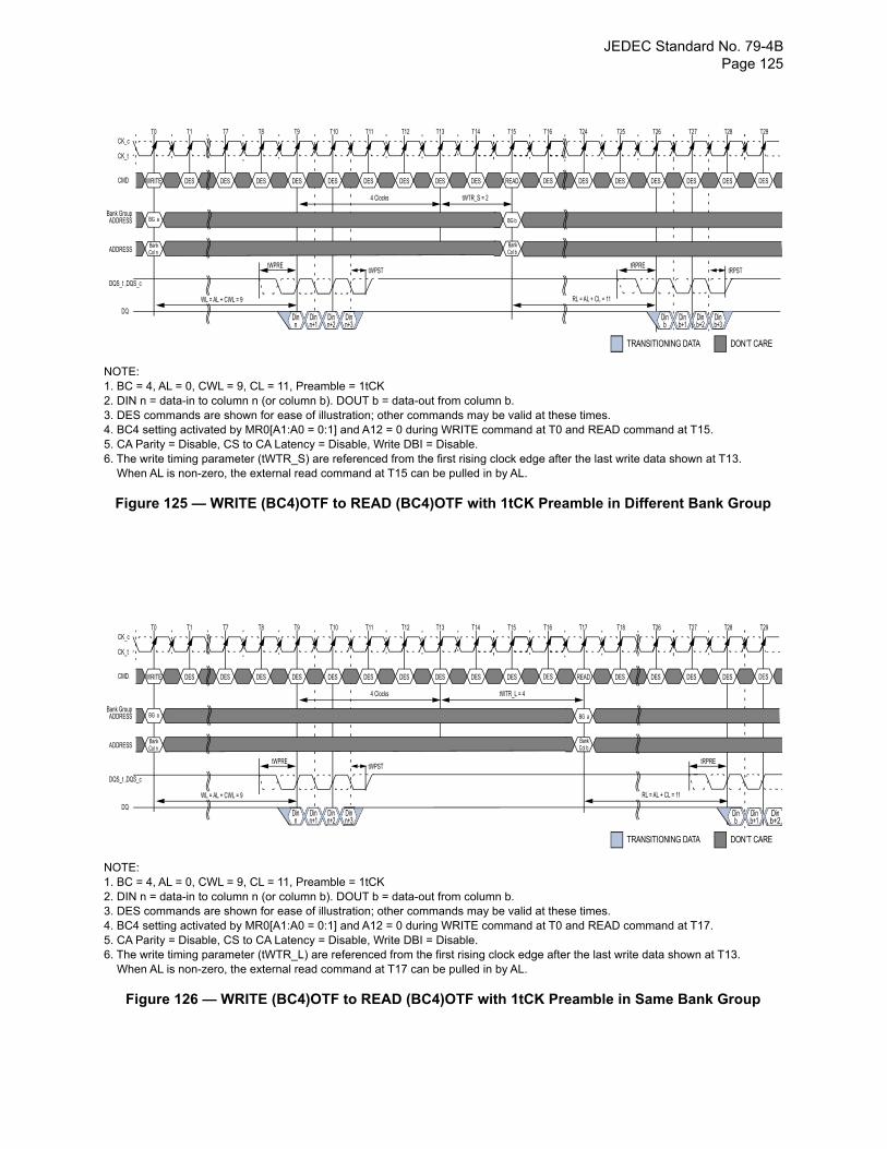
JEDEC Standard No. 79-4B Page 125
NOTE:1. BC = 4, AL = 0, CWL = 9, CL = 11, Preamble = 1tCK2. DIN n = data-in to column n (or column b). DOUT b = data-out from column b.3. DES commands are shown for ease of illustration; other commands may be valid at these times.4. BC4 setting activated by MR0[A1:A0 = 0:1] and A12 = 0 during WRITE command at T0 and READ command at T15.5. CA Parity = Disable, CS to CA Latency = Disable, Write DBI = Disable.6. The write timing parameter (tWTR_S) are referenced from the first rising clock edge after the last write data shown at T13. When AL is non-zero, the external read command at T15 can be pulled in by AL.
Figure 125 — WRITE (BC4)OTF to READ (BC4)OTF with 1tCK Preamble in Different Bank Group
NOTE:1. BC = 4, AL = 0, CWL = 9, CL = 11, Preamble = 1tCK2. DIN n = data-in to column n (or column b). DOUT b = data-out from column b.3. DES commands are shown for ease of illustration; other commands may be valid at these times.4. BC4 setting activated by MR0[A1:A0 = 0:1] and A12 = 0 during WRITE command at T0 and READ command at T17.5. CA Parity = Disable, CS to CA Latency = Disable, Write DBI = Disable.6. The write timing parameter (tWTR_L) are referenced from the first rising clock edge after the last write data shown at T13. When AL is non-zero, the external read command at T17 can be pulled in by AL.
Figure 126 — WRITE (BC4)OTF to READ (BC4)OTF with 1tCK Preamble in Same Bank Group
WRITE
CK_c
CK_t
CMD
DQS_t ,DQS_c
DQ
T0 T1 T8 T9 T10 T11T7 T12 T13 T14 T15
DES DES DES DES DES DES DES DES DES DES
BG aADDRESS
tWPREtWPST
WL = AL + CWL = 9
T16 T24
READ DES
Bank Group
BankADDRESS Col n
Dinn
Dinn+2
Dinn+3
Dinn+1
DON’T CARETRANSITIONING DATA
T25 T26 T28 T29T27
DES DES DES DES DES
BankCol b
4 Clocks
BG b
tRPREtRPST
Dinb
Dinb+2
Dinb+3
Dinb+1
RL = AL + CL = 11
tWTR_S = 2
WRITE
CK_c
CK_t
CMD
DQS_t ,DQS_c
DQ
T0 T1 T8 T9 T10 T11T7 T12 T13 T14 T15
DES DES DES DES DES DES DES DES DES READ
BG aADDRESS
tWPREtWPST
WL = AL + CWL = 9
T16 T17
DES DES
Bank Group
BankADDRESS Col n
Dinn
Dinn+2
Dinn+3
Dinn+1
DON’T CARETRANSITIONING DATA
T18 T26 T28 T29T27
DES DES DES DES DES
BankCol b
4 Clocks
BG a
tRPRE
Dinb
Dinb+2
Dinb+1
RL = AL + CL = 11
tWTR_L = 4
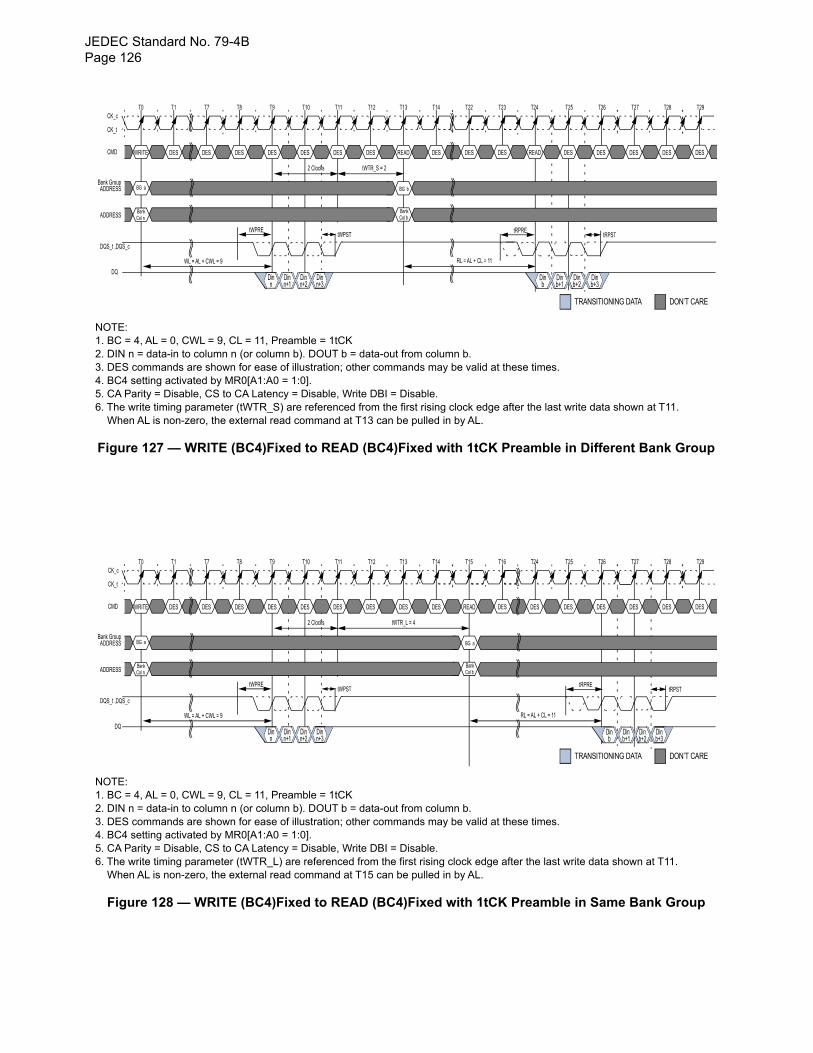
JEDEC Standard No. 79-4BPage 126
NOTE:1. BC = 4, AL = 0, CWL = 9, CL = 11, Preamble = 1tCK2. DIN n = data-in to column n (or column b). DOUT b = data-out from column b.3. DES commands are shown for ease of illustration; other commands may be valid at these times.4. BC4 setting activated by MR0[A1:A0 = 1:0].5. CA Parity = Disable, CS to CA Latency = Disable, Write DBI = Disable.6. The write timing parameter (tWTR_S) are referenced from the first rising clock edge after the last write data shown at T11. When AL is non-zero, the external read command at T13 can be pulled in by AL.
Figure 127 — WRITE (BC4)Fixed to READ (BC4)Fixed with 1tCK Preamble in Different Bank Group
NOTE:1. BC = 4, AL = 0, CWL = 9, CL = 11, Preamble = 1tCK2. DIN n = data-in to column n (or column b). DOUT b = data-out from column b.3. DES commands are shown for ease of illustration; other commands may be valid at these times.4. BC4 setting activated by MR0[A1:A0 = 1:0].5. CA Parity = Disable, CS to CA Latency = Disable, Write DBI = Disable.6. The write timing parameter (tWTR_L) are referenced from the first rising clock edge after the last write data shown at T11. When AL is non-zero, the external read command at T15 can be pulled in by AL.
Figure 128 — WRITE (BC4)Fixed to READ (BC4)Fixed with 1tCK Preamble in Same Bank Group
WRITE
CK_c
CK_t
CMD
DQS_t ,DQS_c
DQ
T0 T1 T8 T9 T10 T11T7 T12 T13 T14 T22
DES DES DES DES DES DES DES READ DES READ
BG aADDRESS
tWPREtWPST
WL = AL + CWL = 9
T23 T24
DES DES
Bank Group
BankADDRESS Col n
Dinn
Dinn+2
Dinn+3
Dinn+1
DON’T CARETRANSITIONING DATA
T25 T26 T28 T29T27
DES DES DES DES DES
BankCol b
2 Clocks
BG b
Dinb
Dinb+2
Dinb+3
Dinb+1
RL = AL + CL = 11
tWTR_S = 2
tRPREtRPST
WRITE
CK_c
CK_t
CMD
DQS_t ,DQS_c
DQ
T0 T1 T8 T9 T10 T11T7 T12 T13 T14 T15
DES DES DES DES DES DES DES DES DES DES
BG aADDRESS
tWPREtWPST
WL = AL + CWL = 9
T16 T24
READ DES
Bank Group
BankADDRESS Col n
Dinn
Dinn+2
Dinn+3
Dinn+1
DON’T CARETRANSITIONING DATA
T25 T26 T28 T29T27
DES DES DES DES DES
BankCol b
2 Clocks
BG a
Dinb
Dinb+2
Dinb+3
Dinb+1
RL = AL + CL = 11
tWTR_L = 4
tRPREtRPST
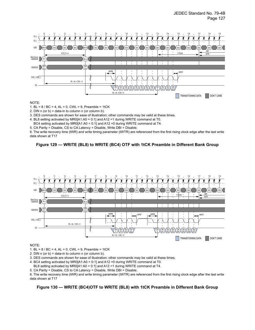
JEDEC Standard No. 79-4B Page 127
NOTE:1. BL = 8 / BC = 4, AL = 0, CWL = 9, Preamble = 1tCK2. DIN n (or b) = data-in to column n (or column b).3. DES commands are shown for ease of illustration; other commands may be valid at these times.4. BL8 setting activated by MR0[A1:A0 = 0:1] and A12 =1 during WRITE command at T0. BC4 setting activated by MR0[A1:A0 = 0:1] and A12 =0 during WRITE command at T4.5. CA Parity = Disable, CS to CA Latency = Disable, Write DBI = Disable.6. The write recovery time (tWR) and write timing parameter (tWTR) are referenced from the first rising clock edge after the last write data shown at T17
Figure 129 — WRITE (BL8) to WRITE (BC4) OTF with 1tCK Preamble in Different Bank Group
NOTE:1. BL = 8 / BC = 4, AL = 0, CWL = 9, Preamble = 1tCK2. DIN n (or b) = data-in to column n (or column b).3. DES commands are shown for ease of illustration; other commands may be valid at these times.4. BC4 setting activated by MR0[A1:A0 = 0:1] and A12 =0 during WRITE command at T0. BL8 setting activated by MR0[A1:A0 = 0:1] and A12 =1 during WRITE command at T4.5. CA Parity = Disable, CS to CA Latency = Disable, Write DBI = Disable.6. The write recovery time (tWR) and write timing parameter (tWTR) are referenced from the first rising clock edge after the last write data shown at T17
Figure 130 — WRITE (BC4)OTF to WRITE (BL8) with 1tCK Preamble in Different Bank Group
WRITE
CK_c
CK_t
CMD
DQS_t ,DQS_c
DQ
T0 T1 T3 T4 T7 T8T2 T9 T10 T11 T12
DES DES DES WRITE DES DES DES DES DES DES
BG aADDRESS
tWPRE tWPST
WL = AL + CWL = 9
T13 T14
DES DES
Bank Group
BankADDRESS Col n
Dinn
Dinn+2
Dinn+3
Dinn+1
Dinn+4
Dinn+5
Dinn+6
Dinn+7
DON’T CARETRANSITIONING DATA
T15 T16 T18 T19T17
DES DES DES DES DES
BG b
BankCol b
Dinb
Dinb+2
Dinb+3
Dinb+1
WL = AL +CWL = 9
tCCD_S = 4 4 ClockstWR
tWTR
WRITE
CK_c
CK_t
CMD
DQS_t ,DQS_c
DQ
T0 T1 T3 T4 T7 T8T2 T9 T10 T11 T12
DES DES DES WRITE DES DES DES DES DES DES
BG aADDRESS
tWPRE tWPST
WL = AL + CWL = 9
T13 T14
DES DES
Bank Group
BankADDRESS Col n
DON’T CARETRANSITIONING DATA
T15 T16 T18 T19T17
DES DES DES DES DES
BG b
BankCol b
tCCD_S = 4
tWPREtWPST
Dinn
Dinn+2
Dinn+3
Dinn+1
Dinb
Dinb+2
Dinb+3
Dinb+1
Dinb+4
Dinb+5
Dinb+6
Dinb+7
tWRtWTR
4 Clocks
WL = AL + CWL = 9
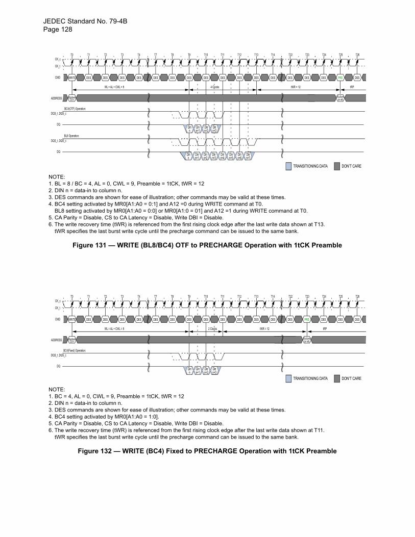
JEDEC Standard No. 79-4BPage 128
NOTE:1. BL = 8 / BC = 4, AL = 0, CWL = 9, Preamble = 1tCK, tWR = 122. DIN n = data-in to column n.3. DES commands are shown for ease of illustration; other commands may be valid at these times.4. BC4 setting activated by MR0[A1:A0 = 0:1] and A12 =0 during WRITE command at T0. BL8 setting activated by MR0[A1:A0 = 0:0] or MR0[A1:0 = 01] and A12 =1 during WRITE command at T0.5. CA Parity = Disable, CS to CA Latency = Disable, Write DBI = Disable.6. The write recovery time (tWR) is referenced from the first rising clock edge after the last write data shown at T13. tWR specifies the last burst write cycle until the precharge command can be issued to the same bank.
Figure 131 — WRITE (BL8/BC4) OTF to PRECHARGE Operation with 1tCK Preamble
NOTE:1. BC = 4, AL = 0, CWL = 9, Preamble = 1tCK, tWR = 122. DIN n = data-in to column n.3. DES commands are shown for ease of illustration; other commands may be valid at these times.4. BC4 setting activated by MR0[A1:A0 = 1:0].5. CA Parity = Disable, CS to CA Latency = Disable, Write DBI = Disable.6. The write recovery time (tWR) is referenced from the first rising clock edge after the last write data shown at T11. tWR specifies the last burst write cycle until the precharge command can be issued to the same bank.
Figure 132 — WRITE (BC4) Fixed to PRECHARGE Operation with 1tCK Preamble
WRITE
CK_c
CK_t
CMD
DQS_t ,DQS_c
DQ
T0 T1 T3 T4 T7 T8T2 T9 T10 T11 T12
DES DES DES DES DES DES DES DES DES DES
ADDRESS
T13 T14
DES DES
Dinn
Dinn+2
Dinn+3
Dinn+1
Dinn+4
Dinn+5
Dinn+6
Dinn+7
DON’T CARETRANSITIONING DATA
T22 T23 T25 T26T24
DES DES DES PRE DES
Dinn
Dinn+2
Dinn+3
Dinn+1
(or all)Col n
WL = AL + CWL = 9
BC4(OTF) Operation:
DQS_t ,DQS_c
DQ
BL8 Operation:
tWR = 124 Clocks tRP
BGa,Bankb BGa,Bankb
WRITE
CK_c
CK_t
CMD
DQS_t ,DQS_c
DQ
T0 T1 T3 T4 T7 T8T2 T9 T10 T11 T12
DES DES DES DES DES DES DES DES DES DES
ADDRESS
T13 T14
DES DES
DON’T CARETRANSITIONING DATA
T22 T23 T25 T26T24
DES PRE DES DES DES
Dinn
Dinn+2
Dinn+3
Dinn+1
(or all)Col n
WL = AL + CWL = 9
BC4(Fixed) Operation:
tWR = 122 Clocks tRP
BGa,Bankb BGa,Bankb
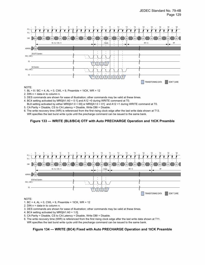
JEDEC Standard No. 79-4B Page 129
NOTE:1. BL = 8 / BC = 4, AL = 0, CWL = 9, Preamble = 1tCK, WR = 122. DIN n = data-in to column n.3. DES commands are shown for ease of illustration; other commands may be valid at these times.4. BC4 setting activated by MR0[A1:A0 = 0:1] and A12 =0 during WRITE command at T0. BL8 setting activated by either MR0[A1:0 = 00] or MR0[A1:0 = 01] and A12 =1 during WRITE command at T0.5. CA Parity = Disable, CS to CA Latency = Disable, Write DBI = Disable.6. The write recovery time (WR) is referenced from the first rising clock edge after the last write data shown at T13. WR specifies the last burst write cycle until the precharge command can be issued to the same bank.
Figure 133 — WRITE (BL8/BC4) OTF with Auto PRECHARGE Operation and 1tCK Preamble
NOTE:1. BC = 4, AL = 0, CWL = 9, Preamble = 1tCK, WR = 122. DIN n = data-in to column n.3. DES commands are shown for ease of illustration; other commands may be valid at these times.4. BC4 setting activated by MR0[A1:A0 = 1:0].5. CA Parity = Disable, CS to CA Latency = Disable, Write DBI = Disable.6. The write recovery time (tWR) is referenced from the first rising clock edge after the last write data shown at T11. WR specifies the last burst write cycle until the precharge command can be issued to the same bank.
Figure 134 — WRITE (BC4) Fixed with Auto PRECHARGE Operation and 1tCK Preamble
WRITE
CK_c
CK_t
CMD
DQS_t ,DQS_c
DQ
T0 T1 T3 T4 T7 T8T2 T9 T10 T11 T12
DES DES DES DES DES DES DES DES DES DES
ADDRESS
T13 T14
DES DES
Dinn
Dinn+2
Dinn+3
Dinn+1
Dinn+4
Dinn+5
Dinn+6
Dinn+7
DON’T CARETRANSITIONING DATA
T22 T23 T25 T26T24
DES DES DES DES DES
Dinn
Dinn+2
Dinn+3
Dinn+1
Col n
WL = AL + CWL = 9
BC4(OTF) Operation:
DQS_t ,DQS_c
DQ
BL8 Operation:
WR = 124 Clocks tRP
BGa,Bankb
WRA
CK_c
CK_t
CMD
DQS_t ,DQS_c
DQ
T0 T1 T3 T4 T7 T8T2 T9 T10 T11 T12
DES DES DES DES DES DES DES DES DES DES
ADDRESS
T13 T14
DES DES
DON’T CARETRANSITIONING DATA
T22 T23 T25 T26T24
DES DES DES DES DES
Dinn
Dinn+2
Dinn+3
Dinn+1
Col n
WL = AL + CWL = 9
BC4(Fixed) Operation:
WR = 122 Clocks tRP
BGa,Bankb
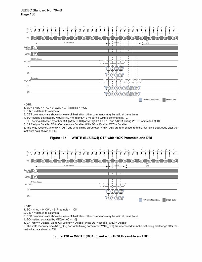
JEDEC Standard No. 79-4BPage 130
NOTE:1. BL = 8 / BC = 4, AL = 0, CWL = 9, Preamble = 1tCK2. DIN n = data-in to column n.3. DES commands are shown for ease of illustration; other commands may be valid at these times.4. BC4 setting activated by MR0[A1:A0 = 0:1] and A12 =0 during WRITE command at T0. BL8 setting activated by either MR0[A1:A0 = 0:0] or MR0[A1:A0 = 0:1] and A12 =1 during WRITE command at T0.5. CA Parity = Disable, CS to CA Latency = Disable, Write DBI = Enable, CRC = Disable.6. The write recovery time (tWR_DBI) and write timing parameter (tWTR_DBI) are referenced from the first rising clock edge after the last write data shown at T13.
Figure 135 — WRITE (BL8/BC4) OTF with 1tCK Preamble and DBI
NOTE:1. BC = 4, AL = 0, CWL = 9, Preamble = 1tCK2. DIN n = data-in to column n.3. DES commands are shown for ease of illustration; other commands may be valid at these times.4. BC4 setting activated by MR0[A1:A0 = 1:0].5. CA Parity = Disable, CS to CA Latency = Disable, Write DBI = Enable, CRC = Disable.6. The write recovery time (tWR_DBI) and write timing parameter (tWTR_DBI) are referenced from the first rising clock edge after the last write data shown at T11.
Figure 136 — WRITE (BC4) Fixed with 1tCK Preamble and DBI
WRITE
CK_c
CK_t
CMD
DQS_t ,DQS_c
T0 T1 T3 T4 T5 T6T2 T7 T8 T9 T10
DES DES DES DES DES DES DES DES DES DES
T11 T12
DES DES
Dinn
Dinn+2
Dinn+3
Dinn+1
Dinn+4
Dinn+5
Dinn+6
Dinn+7
DON’T CARETRANSITIONING DATA
T13 T14 T16 T17T15
DES DES DES DES DES
BG a
WL = AL + CWL = 9
BC4(OTF) Operation:
DQS_t,DQS_c
DQ
BL8 Operation:
4 ClockstWR
tWTR
ADDRESSBank,Col n
Bank GroupADDRES
DQDinn
Dinn+2
Dinn+3
Dinn+1
DBI_nDinn
Dinn+2
Dinn+3
Dinn+1
Dinn
Dinn+2
Dinn+3
Dinn+1
Dinn+4
Dinn+5
Dinn+6
Dinn+7
DBI_n
WRITE
CK_c
CK_t
CMD
DQS_t ,DQS_c
T0 T1 T3 T4 T5 T6T2 T7 T8 T9 T10
DES DES DES DES DES DES DES DES DES DES
T11 T12
DES DES
DON’T CARETRANSITIONING DATA
T13 T14 T16 T17T15
DES DES DES DES DES
BG a
WL = AL + CWL = 9
BC4(Fixed) Operation:
2 ClockstWR
tWTR
ADDRESSBank,Clo n
Banak GroupADDRES
DQDinn
Dinn+2
Dinn+3
Dinn+1
DBI_nDinn
Dinn+2
Dinn+3
Dinn+1
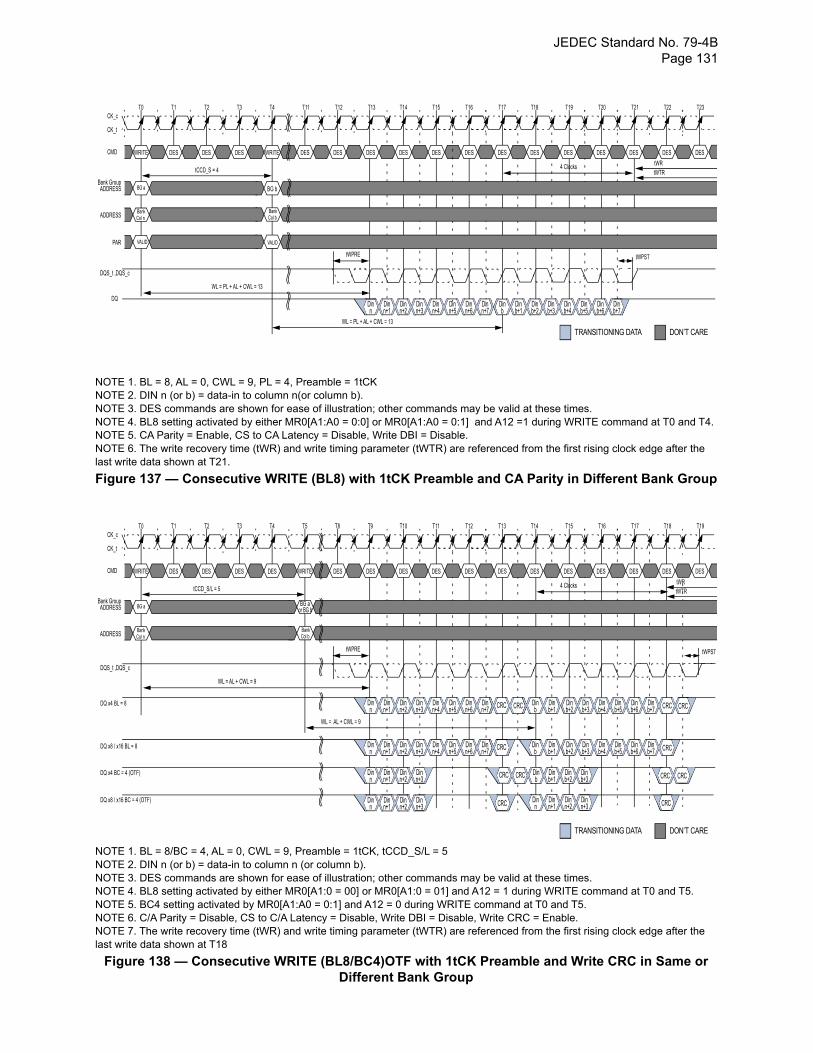
JEDEC Standard No. 79-4B Page 131
NOTE 1. BL = 8, AL = 0, CWL = 9, PL = 4, Preamble = 1tCKNOTE 2. DIN n (or b) = data-in to column n(or column b).NOTE 3. DES commands are shown for ease of illustration; other commands may be valid at these times.NOTE 4. BL8 setting activated by either MR0[A1:A0 = 0:0] or MR0[A1:A0 = 0:1] and A12 =1 during WRITE command at T0 and T4.NOTE 5. CA Parity = Enable, CS to CA Latency = Disable, Write DBI = Disable.NOTE 6. The write recovery time (tWR) and write timing parameter (tWTR) are referenced from the first rising clock edge after the last write data shown at T21.
Figure 137 — Consecutive WRITE (BL8) with 1tCK Preamble and CA Parity in Different Bank Group
NOTE 1. BL = 8/BC = 4, AL = 0, CWL = 9, Preamble = 1tCK, tCCD_S/L = 5 NOTE 2. DIN n (or b) = data-in to column n (or column b).NOTE 3. DES commands are shown for ease of illustration; other commands may be valid at these times.NOTE 4. BL8 setting activated by either MR0[A1:0 = 00] or MR0[A1:0 = 01] and A12 = 1 during WRITE command at T0 and T5.NOTE 5. BC4 setting activated by MR0[A1:A0 = 0:1] and A12 = 0 during WRITE command at T0 and T5.NOTE 6. C/A Parity = Disable, CS to C/A Latency = Disable, Write DBI = Disable, Write CRC = Enable.NOTE 7. The write recovery time (tWR) and write timing parameter (tWTR) are referenced from the first rising clock edge after the last write data shown at T18
Figure 138 — Consecutive WRITE (BL8/BC4)OTF with 1tCK Preamble and Write CRC in Same or Different Bank Group
WRITE
CK_c
CK_t
CMD
DQS_t ,DQS_c
DQ
T0 T1 T3 T4 T11 T12T2 T13 T14 T15 T16
DES DES DES WRITE DES DES DES DES DES DES
BG aADDRESS
tWPRE tWPST
WL = PL + AL + CWL = 13
T17 T18
DES DES
Bank Group
BankADDRESS Col n
Dinn
Dinn+2
Dinn+3
Dinn+1
Dinn+4
Dinn+5
Dinn+6
Dinn+7
DON’T CARETRANSITIONING DATA
T19 T20 T22 T23T21
DES DES DES DES DES
BG b
BankCol b
Dinb
Dinb+2
Dinb+3
Dinb+1
Dinb+4
Dinb+5
Dinb+6
Dinb+7
tCCD_S = 4tWRtWTR
4 Clocks
PAR VALID VALID
WL = PL + AL + CWL = 13
Dinb
WRITE
CK_c
CK_t
CMD
DQS_t ,DQS_c
DQ x4 BL = 8
T0 T1 T3 T4 T5 T8T2 T9 T10 T11 T12
DES DES DES DES WRITE DES DES DES DES DES
BG aADDRESS
tWPRE tWPST
WL = AL + CWL = 9
T13 T14
DES DES
Bank Group
BankADDRESS Col n
Dinn
Dinn+2
Dinn+3
Dinn+1
Dinn+4
Dinn+5
Dinn+6
Dinn+7
DON’T CARETRANSITIONING DATA
T15 T16 T18 T19T17
DES DES DES DES DES
BG a
BankCol b
Dinb+2
Dinb+4
Dinb+5
Dinb+3
Dinb+6
Dinb+7
tCCD_S/L = 5tWRtWTR
4 Clocks
WL = AL + CWL = 9
CRC Dinb
Dinb+1CRC CRC CRC
DQ x8 / x16 BL = 8 Dinn
Dinn+2
Dinn+3
Dinn+1
Dinn+4
Dinn+5
Dinn+6
Dinn+7
Dinb+2
Dinb+4
Dinb+5
Dinb+3
Dinb+6
Dinb+7CRC Din
bDinb+1 CRC
Dinn
Dinn+2
Dinn+3
Dinn+1 CRC Din
b+2Dinb+3
Dinb+1 CRCCRCCRC
Dinn
Dinn+2
Dinn+3
Dinn+1 CRC Din
nDinn+2
Dinn+3
Dinn+1 CRC
DQ x4 BC = 4 (OTF)
DQ x8 / x16 BC = 4 (OTF)
or BG b
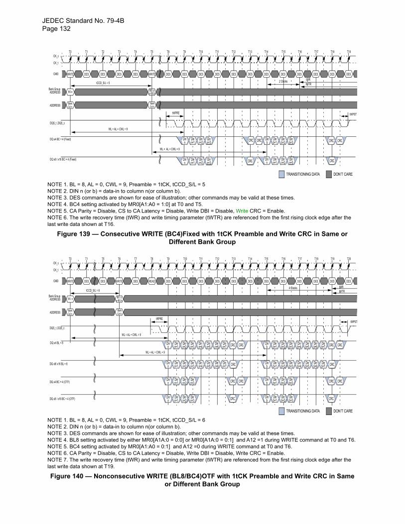
JEDEC Standard No. 79-4BPage 132
NOTE 1. BL = 8, AL = 0, CWL = 9, Preamble = 1tCK, tCCD_S/L = 5NOTE 2. DIN n (or b) = data-in to column n(or column b).NOTE 3. DES commands are shown for ease of illustration; other commands may be valid at these times.NOTE 4. BC4 setting activated by MR0[A1:A0 = 1:0] at T0 and T5.NOTE 5. CA Parity = Disable, CS to CA Latency = Disable, Write DBI = Disable, Write CRC = Enable.NOTE 6. The write recovery time (tWR) and write timing parameter (tWTR) are referenced from the first rising clock edge after the last write data shown at T16.
Figure 139 — Consecutive WRITE (BC4)Fixed with 1tCK Preamble and Write CRC in Same or Different Bank Group
NOTE 1. BL = 8, AL = 0, CWL = 9, Preamble = 1tCK, tCCD_S/L = 6NOTE 2. DIN n (or b) = data-in to column n(or column b).NOTE 3. DES commands are shown for ease of illustration; other commands may be valid at these times.NOTE 4. BL8 setting activated by either MR0[A1A:0 = 0:0] or MR0[A1A:0 = 0:1] and A12 =1 during WRITE command at T0 and T6.NOTE 5. BC4 setting activated by MR0[A1:A0 = 0:1] and A12 =0 during WRITE command at T0 and T6.NOTE 6. CA Parity = Disable, CS to CA Latency = Disable, Write DBI = Disable, Write CRC = Enable.NOTE 7. The write recovery time (tWR) and write timing parameter (tWTR) are referenced from the first rising clock edge after the last write data shown at T19.
Figure 140 — Nonconsecutive WRITE (BL8/BC4)OTF with 1tCK Preamble and Write CRC in Same or Different Bank Group
Dinb
WRITE
CK_c
CK_t
CMD
DQS_t ,DQS_c
T0 T1 T3 T4 T5 T8T2 T9 T10 T11 T12
DES DES DES DES WRITE DES DES DES DES DES
BG aADDRESS
tWPRE tWPST
WL = AL + CWL = 9
T13 T14
DES DES
Bank Group
BankADDRESS Col n
DON’T CARETRANSITIONING DATA
T15 T16 T18 T19T17
DES DES DES DES DES
BG a
BankCol b
tCCD_S/L = 5tWRtWTR
2 Clocks
WL = AL + CWL = 9
Dinn
Dinn+2
Dinn+3
Dinn+1 CRC Din
b+2Dinb+3
Dinb+1 CRCCRCCRC
Dinn
Dinn+2
Dinn+3
Dinn+1 CRC Din
nDinn+2
Dinn+3
Dinn+1 CRC
DQ x4 BC = 4 (Fixed)
DQ x8 / x16 BC = 4 (Fixed)
or BG b
WRITE
CK_c
CK_t
CMD
DQS_t ,DQS_c
DQ x4 BL = 8
T0 T1 T6 T7 T8 T9T5 T10 T11 T12 T13
DES DES WRITE DES READ DES DES DES DES DES
BG aADDRESS
tRPRE
WL = AL + CWL = 9
T14 T15
DES DES
Bank Group
BankADDRESS Col n
DON’T CARETRANSITIONING DATA
T16 T17 T19 T20T18
DES DES DES DES DES
BG a
BankCol b
Dinb
Dinb+2 CRCDin
b+1
or BG b
tCCD_S/L = 6
tWPST
4 Clocks tWRtWTR
Dinb+4
Dinb+3
Dinb+6
Dinb+5 CRCDin
b+7
DQ x8/ x16 BL = 8 Dinb
Dinb+2 CRCDin
b+1Dinb+4
Dinb+3
Dinb+6
Dinb+5
Dinb+7
Dinn
Dinn+2 CRCDin
n+1Dinn+3 CRC
Dinb
Dinb+2
Dinb+1
Dinb+3 CRC
DQ x4 BC = 4 (OTF)
WL = AL + CWL = 9
Dinn
Dinn+2 CRCDin
n+1Dinn+4
Dinn+3
Dinn+6
Dinn+5
Dinn+7
Dinn
Dinn+2 CRCDin
n+1Dinn+4
Dinn+3
Dinn+6
Dinn+5 CRCDin
n+7
Dinb
Dinb+2
Dinb+1
Dinb+3 CRCCRC
Dinn
Dinn+2
Dinn+1
Dinn+3 CRCDQ x8 / x16 BC = 4 (OTF)
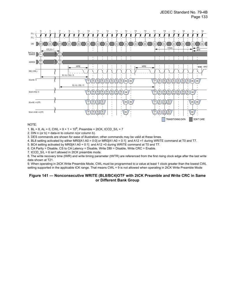
JEDEC Standard No. 79-4B Page 133
NOTE:
1. BL = 8, AL = 0, CWL = 9 + 1 = 109, Preamble = 2tCK, tCCD_S/L = 72. DIN n (or b) = data-in to column n(or column b).3. DES commands are shown for ease of illustration; other commands may be valid at these times.4. BL8 setting activated by either MR0[A1:A0 = 0:0] or MR0[A1:A0 = 0:1] and A12 =1 during WRITE command at T0 and T7.5. BC4 setting activated by MR0[A1:A0 = 0:1] and A12 =0 during WRITE command at T0 and T7.6. CA Parity = Disable, CS to CA Latency = Disable, Write DBI = Disable, Write CRC = Enable.7. tCCD_S/L = 6 isn’t allowed in 2tCK preamble mode.8. The write recovery time (tWR) and write timing parameter (tWTR) are referenced from the first rising clock edge after the last write data shown at T21. 9. When operating in 2tCK Write Preamble Mode, CWL must be programmed to a value at least 1 clock greater than the lowest CWL setting supported in the applicable tCK range. That means CWL = 9 is not allowed when operating in 2tCK Write Preamble Mode
Figure 141 — Nonconsecutive WRITE (BL8/BC4)OTF with 2tCK Preamble and Write CRC in Same or Different Bank Group
WRITE
CK_c
CK_t
CMD
DQS_t ,DQS_c
DQ x4 BL = 8
T0 T1 T8 T9 T10 T11T7 T12 T13 T14 T15
DES WRITE DES DES DES DES DES DES DES DES
BG aADDRESS
T16 T17
DES DES
Bank Group
BankADDRESS Col n
DON’T CARETRANSITIONING DATA
T18 T19 T21 T22T20
DES DES DES DES DES
BG a
BankCol b
Dinb
Dinb+2 CRCDin
b+1
or BG b
tCCD_S/L = 74 Clocks tWR
tWTR
Dinb+4
Dinb+3
Dinb+6
Dinb+5 CRCDin
b+7
DQ x8/ x16 BL = 8 Dinb
Dinb+2 CRCDin
b+1Dinb+4
Dinb+3
Dinb+6
Dinb+5
Dinb+7
Dinn
Dinn+2 CRCDin
n+1Dinn+3 CRC
Dinb
Dinb+2
Dinb+1
Dinb+3 CRC
DQ x4 BC = 4 (OTF)
WL = AL + CWL = 10
Dinn
Dinn+2 CRCDin
n+1Dinn+4
Dinn+3
Dinn+6
Dinn+5
Dinn+7
Dinn
Dinn+2 CRCDin
n+1Dinn+4
Dinn+3
Dinn+6
Dinn+5 CRCDin
n+7
Dinb
Dinb+2
Dinb+1
Dinb+3 CRCCRC
Dinn
Dinn+2
Dinn+1
Dinn+3 CRCDQ x8 / x16 BC = 4 (OTF)
tWPRE
WL = AL + CWL = 10
tWPSTtWPRE
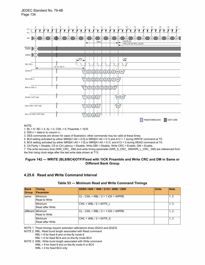
JEDEC Standard No. 79-4BPage 134
NOTE:1. BL = 8 / BC = 4, AL = 0, CWL = 9, Preamble = 1tCK2. DIN n = data-in to column n.3. DES commands are shown for ease of illustration; other commands may be valid at these times.4. BL8 setting activated by either MR0[A1:A0 = 0:0] or MR0[A1:A0 = 0:1] and A12 = 1 during WRITE command at T0.5. BC4 setting activated by either MR0[A1:A0 = 1:0] or MR0[A1:A0 = 0:1] and A12 = 0 during READ command at T0.6. CA Parity = Disable, CS to CA Latency = Disable, Write DBI = Disable, Write CRC = Enable, DM = Enable.7. The write recovery time (tWR_CRC_ DM) and write timing parameter (tWR_S_CRC_ DM/tWR_L_CRC_ DM) are referenced from the first rising clock edge after the last write data shown at T13.
Figure 142 — WRITE (BL8/BC4)OTF/Fixed with 1tCK Preamble and Write CRC and DM in Same or Different Bank Group
4.25.6 Read and Write Command Interval
Table 53 — Minimum Read and Write Command Timings
NOTE 1. These timings require extended calibrations times tZQinit and tZQCS.NOTE 2. RBL: Read burst length associated with Read command RBL = 8 for fixed 8 and on-the-fly mode 8 RBL = 4 for fixed BC4 and on-the-fly mode BC4NOTE 3. WBL: Write burst length associated with Write command WBL = 8 for fixed 8 and on-the-fly mode 8 or BC4 WBL = 4 for fixed BC4 only
BankGroup
TimingParameter
DDR4-1600 / 1866 / 2133 / 2666 / 3200 Units Note
same MinimumRead to Write
CL - CWL + RBL / 2 + 1 tCK + tWPRE 1, 2
MinimumRead after Write
CWL + WBL / 2 + tWTR_L 1, 3
different MinimumRead to Write
CL - CWL + RBL / 2 + 1 tCK + tWPRE 1, 2
MinimumRead after Write
CWL + WBL / 2 + tWTR_S 1, 3
WRITE
CK_c
CK_t
CMD
DQS_t ,DQS_c
DQ x4 BL = 8
T0 T1 T6 T7 T8 T9T2 T10 T11 T12 T13
DES DES DES DES DES DES DES DES DES DES
BG aADDRESS
T14 T15
DES DES
Bank Group
BankADDRESS Col n
DON’T CARETRANSITIONING DATA
T16 T17 T19 T20T18
DES DES DES DES DES
4 Clocks tWR_CRC_DM
tWTR_S_CRC_DM / tWTR_L_CRC_DM
DQ x8/ x16 BL = 8
Dinn
Dinn+2 CRCDin
n+1Dinn+3 CRCDQ x4 BC = 4 (OTF / Fixed)
Dinn
Dinn+2 CRCDin
n+1Dinn+4
Dinn+3
Dinn+6
Dinn+5
Dinn+7
Dinn
Dinn+2 CRCDin
n+1Dinn+4
Dinn+3
Dinn+6
Dinn+5 CRCDin
n+7
Dinn
Dinn+2
Dinn+1
Dinn+3 CRCDQ x8 / x16 BC = 4 (OTF / Fixed)
WL = AL + CWL = 9
tWPSTtWPRE
DMn
DMn+2
DMn+3
DMn+1
DMn+4
DMn+5
DMn+6
DMn+7
DMx4 / x8 / x16 BL = 8
DMn
DMn+2
DMn+1
DMn+3
DM x4 / x8 / x16 BC = 4 (OTF / Fixed)
JEDEC Standard No. 79-4B Page 135
4.25.7 Write Timing Violations
4.25.7.1 MotivationGenerally, if Write timing parameters are violated, a complete reset/initialization procedure has to be initiated to make sure that the DRAM works properly. However, it is desirable, for certain violations as specified below, the DRAM is guaranteed to not “hang up,” and that errors are limited to that particular operation.For the following, it will be assumed that there are no timing violations with regards to the Write command itself (including ODT, etc.) and that it does satisfy all timing requirements not mentioned below.
4.25.7.2 Data Setup and Hold Offset ViolationsShould the data to strobe timing requirements (Tdqs_off, Tdqh_off, Tdqs_dd_off, Tdqh_dd_off) be violated, for any of the strobe edges associated with a write burst, then wrong data might be written to the memory locations addressed with this WRITE command.In the example (Figure 114), the relevant strobe edges for write burst A are associated with the clock edges: T9, T9.5, T10, T10.5, T11, T11.5, T12, T12.5.Subsequent reads from that location might results in unpredictable read data, however the DRAM will work properly otherwise.
4.25.7.3 Strobe and Strobe to Clock Timing ViolationsShould the strobe timing requirements (tDQSH, tDQSL, tWPRE, tWPST) or the strobe to clock timing requirements (tDSS, tDSH, tDQSS) be violated for any of the strobe edges associated with a Write burst, then wrong data might be written to the memory location addressed with the offending WRITE command. Subsequent reads from that location might result in unpredictable read data, however the DRAM will work properly otherwise with the following constraints:(1) Both Write CRC and data burst OTF are disabled; timing specifications other than tDQSH, tDQSL, tWPRE, tWPST, tDSS, tDSH, tDQSS are not violated.(2) The offending write strobe (and preamble) arrive no earlier or later than six DQS transition edges from the Write-Latency position.(3) A Read command following an offending Write command from any open bank is allowed.(4) One or more subsequent WR or a subsequent WRA {to same bank as offending WR} may be issued tCCD_L later but incorrect data could be written; subsequent WR and WRA can be either offending or non-offending Writes. Reads from these Writes may provide incorrect data.(5) One or more subsequent WR or a subsequent WRA {to a different bank group} may be issued tCCD_S later but incorrect data could be written; subsequent WR and WRA can be either offending or non-offending Writes. Reads from these Writes may provide incorrect data.(6) Once one or more precharge commands(PRE or PREA) are issued to DDR4 after offending WRITE command and all banks become precharged state(idle state), a subsequent, non-offending WR or WRA to any open bank shall be able to write correct data.
4.26 Refresh Command The Refresh command (REF) is used during normal operation of the DDR4 SDRAMs. This command is non persistent, so it must be issued each time a refresh is required. The DDR4 SDRAM requires Refresh cycles at an average periodic interval of tREFI. When CS_n, RAS_n/A16 and CAS_n/A15 are held Low and WE_n/A14 and ACT_n are held High at the rising edge of the clock, the chip enters a Refresh cycle. All banks of the SDRAM must be precharged and idle for a minimum of the precharge time tRP(min) before the Refresh Command can be applied. The refresh addressing is generated by the internal refresh controller. This makes the address bits “Don’t Care” during a Refresh command. An internal address counter supplies the addresses during the refresh cycle. No control of the external address bus is required once this cycle has started. When the refresh cycle has completed, all banks of the SDRAM will be in the precharged (idle) state. A delay between the Refresh Command and the next valid command, except DES, must be greater than or equal to the minimum Refresh cycle time tRFC(min) as shown in Figure 143. Note that the tRFC timing parameter depends on memory density.
In general, a Refresh command needs to be issued to the DDR4 SDRAM regularly every tREFI interval. To allow for improved efficiency in scheduling and switching between tasks, some flexibility in the absolute refresh interval is provided for postponing and pulling-in refresh command. A maximum of 8 Refresh commands can be postponed when DRAM is in 1X refresh mode and for 2X/4X refresh mode, 16/32 Refresh commands can be postponed respectively during operation of the DDR4 SDRAM, meaning that at no point in time more than a total of 8,16,32 Refresh commands are allowed to be postponed for 1X,2X,4X Refresh mode respectively. In case that 8 Refresh commands are postponed in a row, the resulting maximum interval between the surrounding Refresh commands is limited to 9 × tREFI (see Figure 143). In 2X and 4X Refresh mode, it’s limited to 17 x tREFI2 and 33 x tREFI4. A maximum of 8 additional Refresh commands can be issued in advance (“pulled in”) in 1X refresh mode and for 2X/4X refresh mode, 16/32 Refresh commands can be pulled in respectively, with each one reducing the number of regular Refresh commands required later by one. Note that pulling in more than 8/16/32, depending on Refresh mode, Refresh commands in advance does not further reduce the number of regular Refresh commands required later, so that the resulting maximum interval between two surrounding Refresh commands is limited to 9 × tREFI , 17 x tRFEI2 and 33 x tREFI4 respectively. At any given time, a maximum of 16 REF/32REF 2/64REF 4 commands can be issued within 2 x tREFI/ 4 x tREFI2/ 8 x tREFI4
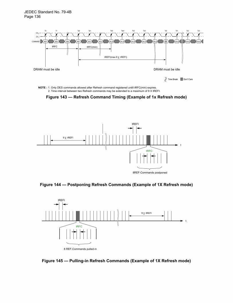
JEDEC Standard No. 79-4BPage 136
Figure 143 — Refresh Command Timing (Example of 1x Refresh mode)
Figure 144 — Postponing Refresh Commands (Example of 1X Refresh mode)
Figure 145 — Pulling-in Refresh Commands (Example of 1X Refresh mode)
DES
Ta0 Tb0 Tab1 Tb2Ta1 Tb3 Tc0 Tc1
REF DES VALID
T1T0
DES
CK_c
CK_t
COMMAND
Tc2 Tc3
VALID VALIDREF DES VALID VALID VALID VALID REF VALID
tRFC tRFC(min)
tREFI(max.9 tREFI)
DRAM must be idle DRAM must be idle
Time Break Don’t Care
NOTE : 1. Only DES commands allowed after Refresh command registered untill tRFC(min) expires. 2. Time interval between two Refresh commands may be extended to a maximum of 9 X tREFI.
tREFI
9 tREFI
8REF-Commands postponed
t
tRFC
tREFI
9 tREFI
8 REF-Commands pulled-in
t
tRFC
JEDEC Standard No. 79-4B Page 137
4.27 Self refresh Operation The Self-Refresh command can be used to retain data in the DDR4 SDRAM, even if the rest of the system is powered down. When in the Self-Refresh mode, the DDR4 SDRAM retains data without external clocking.The DDR4 SDRAM device has a built-in timer to accommodate Self-Refresh operation. The Self-Refresh-Entry (SRE) Command is defined by having CS_n, RAS_n/A16, CAS_n/A15, and CKE held low with WE_n/A14 and ACT_n high at the rising edge of the clock.
Before issuing the Self-Refresh-Entry command, the DDR4 SDRAM must be idle with all bank precharge state with tRP satisfied. ‘Idle state’ is defined as all banks are closed (tRP, tDAL, etc. satisfied), no data bursts are in progress, CKE is high, and all timings from previous operations are satisfied (tMRD, tMOD,tRFC, tZQinit, tZQoper, tZQCS, etc.). Deselect command must be registered on last positive clock edge before issuing Self Refresh Entry command. Once the Self Refresh Entry command is registered, Deselect command must also be registered at the next positive clock edge. Once the Self-Refresh Entry command is registered, CKE must be held low to keep the device in Self-Refresh mode. .DRAM automatically disables ODT termination and set Hi-Z as termination state regardless of ODT pin and RTT_PARK set when it enters in Self-Refresh mode. Upon exiting Self-Refresh, DRAM automatically enables ODT termination and set RTT_PARK asynchronously during tXSDLL when RTT_PARK is enabled. During normal operation (DLL on) the DLL is automatically disabled upon entering Self-Refresh and is automatically enabled (including a DLL-Reset) upon exiting Self-Refresh.
When the DDR4 SDRAM has entered Self-Refresh mode, all of the external control signals, except CKE and RESET_n, are “don’t care.” For proper Self-Refresh operation, all power supply and reference pins (VDD, VDDQ, VSS, VSSQ, VPP, and VRefCA) must be at valid levels. DRAM internal VrefDQ generator circuitry may remain ON or turned OFF depending on DRAM design. If DRAM internal VrefDQ circuitry is turned OFF in self refresh, when DRAM exits from self refresh state, it ensures that VrefDQ generator circuitry is powered up and stable within tXS period. First Write operation or first Write Leveling Activity may not occur earlier than tXS after exit from Self Refresh. The DRAM initiates a minimum of one Refresh command internally within tCKE period once it enters Self-Refresh mode.
The clock is internally disabled during Self-Refresh Operation to save power. The minimum time that the DDR4 SDRAM must remain in Self-Refresh mode is tCKESR. The user may change the external clock frequency or halt the external clock tCKSRE after Self-Refresh entry is registered, however, the clock must be restarted and stable tCKSRX before the device can exit Self-Refresh operation.
The procedure for exiting Self-Refresh requires a sequence of events. First, the clock must be stable prior to CKE going back HIGH. Once a Self-Refresh Exit command (SRX, combination of CKE going high and Deselect on command bus) is registered, following timing delay must be satisfied:
1. Commands that do not require locked DLL:tXS - ACT, PRE, PREA, REF, SRE, PDE, WR, WRS4, WRS8, WRA, WRAS4, WRAS8tXSFast - ZQCL, ZQCS, MRS commands. For MRS command, only DRAM CL and WR/RTP register and DLL Reset in MR0, RTT_NOM register in MR1, CWL and RTT_WR register in MR2 and geardown mode in MR3, Write and Read Preamble register in MR4, RTT_PARK register in MR5, tCCD_L/tDLLK and VrefDQ Training Value in MR6 are allowed to be accessed provided DRAM is not in per DRAM addressability mode. Access to other DRAM mode registers must satisfy tXS timing.Note that synchronous ODT for write commands ( WR, WRS4, WRS8, WRA, WRAS4 and WRAS8 ) and dynamic ODT controlled by write command require locked DLL.
2. Commands that require locked DLL:tXSDLL - RD, RDS4, RDS8, RDA, RDAS4, RDAS8Depending on the system environment and the amount of time spent in Self-Refresh, ZQ calibration commands may be required to compensate for the voltage and temperature drift as described in “ZQ Calibration Commands” on Section 4.12. To issue ZQ calibration commands, applicable timing requirements must be satisfied.
CKE must remain HIGH for the entire Self-Refresh exit period tXSDLL for proper operation except for Self-Refresh re-entry. Upon exit from Self-Refresh, the DDR4 SDRAM can be put back into Self-Refresh mode or Power down mode after waiting at least tXS period and issuing one refresh command (refresh period of tRFC). Deselect commands must be registered on each positive clock edge during the Self-Refresh exit interval tXS. Low level of ODT pin must be registered on each positive clock edge during tXSDLL when normal mode ( DLL-on ) is set. Under DLL-off mode, asynchronous ODT function might be allowed.The use of Self-Refresh mode introduces the possibility that an internally timed refresh event can be missed when CKE is raised for exit from Self-Refresh mode. Upon exit from Self-Refresh, the DDR4 SDRAM requires a minimum of one extra refresh command before it is put back into Self-Refresh Mode.
The exit timing from self-refresh exit to first valid command not requiring a locked DLL is tXS.The value of tXS is (tRFC+10ns). This delay is to allow for any refreshes started by the DRAM to complete. tRFC continues to grow with higher density devices so tXS will grow as well.
A Bit A9 in MR4 is defined to enable the self refresh abort mode. If the bit is disabled then the controller uses tXS timings. If the bit is enabled then the DRAM aborts any ongoing refresh and does not increment the refresh counter. The controller can issue a valid command not requiring a locked DLL after a delay of tXS_abort.
Upon exit from Self-Refresh, the DDR4 SDRAM requires a minimum of one extra refresh command before it is put back into Self-Refresh Mode. This requirement remains the same irrespective of the setting of the MRS bit for self refresh abort.
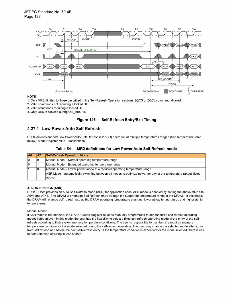
JEDEC Standard No. 79-4BPage 138
.
NOTE : 1. Only MRS (limited to those described in the Self-Refresh Operation section). ZQCS or ZQCL command allowed.2. Valid commands not requiring a locked DLL.3. Valid commands requiring a locked DLL.4. Only DES is allowed during tXS_ABORT.
Figure 146 — Self-Refresh Entry/Exit Timing
4.27.1 Low Power Auto Self Refresh
DDR4 devices support Low Power Auto Self-Refresh (LP ASR) operation at multiple temperatures ranges (See temperature table below). Mode Register MR2 – descriptions
Table 54 — MR2 definitions for Low Power Auto Self-Refresh mode
Auto Self Refresh (ASR)DDR4 DRAM provides an Auto Self-Refresh mode (ASR) for application ease. ASR mode is enabled by setting the above MR2 bits A6=1 and A7=1. The DRAM will manage Self Refresh entry through the supported temperature range of the DRAM. In this mode, the DRAM will change self-refresh rate as the DRAM operating temperature changes, lower at low temperatures and higher at high temperatures.
Manual Modes If ASR mode is not enabled, the LP ASR Mode Register must be manually programmed to one the three self-refresh operating modes listed above. In this mode, the user has the flexibility to select a fixed self-refresh operating mode at the entry of the self-refresh according to their system memory temperature conditions. The user is responsible to maintain the required memory temperature condition for the mode selected during the self-refresh operation. The user may change the selected mode after exiting from self refresh and before the next self-refresh entry. If the temperature condition is exceeded for the mode selected, there is risk to data retention resulting in loss of data.
A6 A7 Self-Refresh Operation Mode
0 0 Manual Mode – Normal operating temperature range
0 1 Manual Mode – Extended operating temperature range
1 0 Manual Mode – Lower power mode at a reduced operating temperature range
1 1 ASR Mode – automatically switching between all modes to optimize power for any of the temperature ranges listed above
T0 T1 Td1Td0Ta0 Tb0 Tc0 Te0 Tf0 Tg0
tIS tCPDED tCKSRE tCKSRX
tCKESR / tCKESR_PAR
DES SRE DES SRX VALID1 VALID2 VALID3
VALID
VALIDVALID
CK_c
CK_t
CKE
ODT
COMMAND
ADDR
tRP
Enter Self Refresh Exit Self Refresh
tXS_ABORT4
tXSDLL
tIS
DON’T CARE TIME BREAK
VALIDVALID
VALID
tXS_FAST
VALIDVALID
ODTL
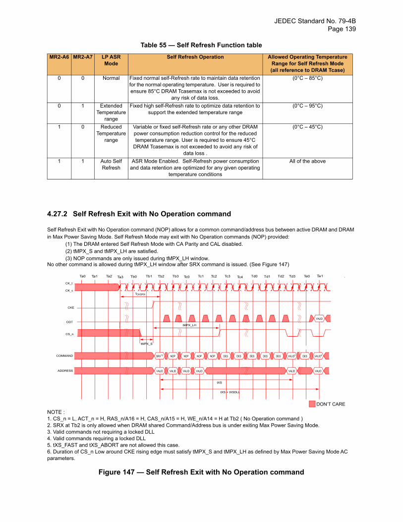
JEDEC Standard No. 79-4B Page 139
Table 55 — Self Refresh Function table
4.27.2 Self Refresh Exit with No Operation command
Self Refresh Exit with No Operation command (NOP) allows for a common command/address bus between active DRAM and DRAM in Max Power Saving Mode. Self Refresh Mode may exit with No Operation commands (NOP) provided:
(1) The DRAM entered Self Refresh Mode with CA Parity and CAL disabled. (2) tMPX_S and tMPX_LH are satisfied. (3) NOP commands are only issued during tMPX_LH window.
No other command is allowed during tMPX_LH window after SRX command is issued. (See Figure 147)
NOTE : 1. CS_n = L, ACT_n = H, RAS_n/A16 = H, CAS_n/A15 = H, WE_n/A14 = H at Tb2 ( No Operation command ) 2. SRX at Tb2 is only allowed when DRAM shared Command/Address bus is under exiting Max Power Saving Mode. 3. Valid commands not requiring a locked DLL 4. Valid commands requiring a locked DLL 5. tXS_FAST and tXS_ABORT are not allowed this case. 6. Duration of CS_n Low around CKE rising edge must satisfy tMPX_S and tMPX_LH as defined by Max Power Saving Mode AC parameters.
Figure 147 — Self Refresh Exit with No Operation command
MR2-A6 MR2-A7 LP ASR Mode
Self Refresh Operation Allowed Operating Temperature Range for Self Refresh Mode(all reference to DRAM Tcase)
0 0 Normal Fixed normal self-Refresh rate to maintain data retention for the normal operating temperature. User is required to ensure 85°C DRAM Tcasemax is not exceeded to avoid
any risk of data loss.
(0°C – 85°C)
0 1 Extended Temperature
range
Fixed high self-Refresh rate to optimize data retention to support the extended temperature range
(0°C – 95°C)
1 0 Reduced Temperature
range
Variable or fixed self-Refresh rate or any other DRAM power consumption reduction control for the reduced temperature range. User is required to ensure 45°C
DRAM Tcasemax is not exceeded to avoid any risk of data loss .
(0°C – 45°C)
1 1 Auto Self Refresh
ASR Mode Enabled. Self-Refresh power consumption and data retention are optimized for any given operating
temperature conditions
All of the above
CK_t
Tb1 . Tb3 . Tc1 . Tc3 . . Td2 . Te0 . .Td0Ta0 . Ta2
CKE
tMPX_S
COMMAND
ODT
tCKSRX
Ta1 Ta3 Tb0 Tb2 Tc0 Tc2 Tc4 Td1 Td3 Te1
VALID
CS_n
SRX1,2 NOP NOP NOP NOP DES DES DES DES DES VALID3 DES VALID4
ADDRESS VALID VALID VALID VALID VALID VALID
tMPX_LH
tXS
tXS + tXSDLL
DON’T CARE
CK_c
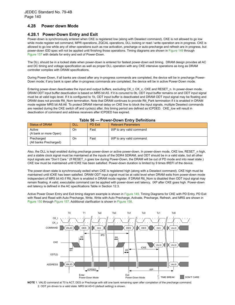
JEDEC Standard No. 79-4BPage 140
4.28 Power down Mode
4.28.1 Power-Down Entry and ExitPower-down is synchronously entered when CKE is registered low (along with Deselect command). CKE is not allowed to go low while mode register set command, MPR operations, ZQCAL operations, DLL locking or read / write operation are in progress. CKE is allowed to go low while any of other operations such as row activation, precharge or auto-precharge and refresh are in progress, but power-down IDD spec will not be applied until finishing those operations. Timing diagrams are shown in Figure 149 through Figure 157 with details for entry and exit of Power-Down.
The DLL should be in a locked state when power-down is entered for fastest power-down exit timing. DRAM design provides all AC and DC timing and voltage specification as well as proper DLL operation with any CKE intensive operations as long as DRAM controller complies with DRAM specifications.
During Power-Down, if all banks are closed after any in-progress commands are completed, the device will be in precharge Power-Down mode; if any bank is open after in-progress commands are completed, the device will be in active Power-Down mode.
Entering power-down deactivates the input and output buffers, excluding CK_t, CK_c, CKE and RESET_n. In power-down mode, DRAM ODT input buffer deactivation is based on MR5 bit A5. If it is conured to 0b, ODT input buffer remains on and ODT input signal must be at valid logic level. If it is configured to 1b, ODT input buffer is deactivated and DRAM ODT input signal may be floating and DRAM does not provide Rtt_Nom termination. Note that DRAM continues to provide Rtt_Park termination if it is enabled in DRAM mode register MR5 bit A8:A6. To protect DRAM internal delay on CKE line to block the input signals, multiple Deselect commands are needed during the CKE switch off and cycle(s) after, this timing period are defined as tCPDED. CKE_low will result in deactivation of command and address receivers after tCPDED has expired.
Table 56 — Power-Down Entry Definitions
Also, the DLL is kept enabled during precharge power-down or active power-down. In power-down mode, CKE low, RESET_n high, and a stable clock signal must be maintained at the inputs of the DDR4 SDRAM, and ODT should be in a valid state, but all other input signals are “Don’t Care.” (If RESET_n goes low during Power-Down, the DRAM will be out of PD mode and into reset state.) CKE low must be maintained until tCKE has been satisfied. Power-down duration is limited by 9 times tREFI of the device.
The power-down state is synchronously exited when CKE is registered high (along with a Deselect command). CKE high must be maintained until tCKE has been satisfied. DRAM ODT input signal must be at valid level when DRAM exits from power-down mode independent of MR5 bit A5 if Rtt_Nom is enabled in DRAM mode register. If DRAM Rtt_Nom is disabled then ODT input signal may remain floating. A valid, executable command can be applied with power-down exit latency, tXP after CKE goes high. Power-down exit latency is defined in the AC specifications Table in Section 12.3.
Active Power Down Entry and Exit timing diagram example is shown in Figure 149. Timing Diagrams for CKE with PD Entry, PD Exit with Read and Read with Auto Precharge, Write, Write with Auto Precharge, Activate, Precharge, Refresh, and MRS are shown in Figure 150 through Figure 157. Additional clarification is shown in Figure 158.
Status of DRAM DLL PD Exit Relevant Parameters
Active(A bank or more Open)
On Fast tXP to any valid command
Precharged(All banks Precharged)
On Fast tXP to any valid command.
DES DES DESVALID
CK_t
CK_c
COMMAND DESDES
CKE
ADDRESS
tXP
T0 T1 Ta0 Tb0 Tb1 Tc0 Tc1 Td0
VALID
tIH
tIS tIH
tIS
VALID VALID
VALID VALID
tCKE
tCPDED
EnterPower-Down Mode
ExitPower-Down Mode
tPD
TIME BREAK DON’T CARE
NOTE 1. VALID command at T0 is ACT, DES or Precharge with still one bank remaining open after completion of the precharge command.
ODT(2)
2. ODT pin driven to a valid state. MR5 bit A5=0 (default setting) is shown.
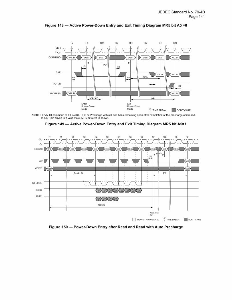
JEDEC Standard No. 79-4B Page 141
Figure 148 — Active Power-Down Entry and Exit Timing Diagram MR5 bit A5 =0
Figure 149 — Active Power-Down Entry and Exit Timing Diagram MR5 bit A5=1
Figure 150 — Power-Down Entry after Read and Read with Auto Precharge
DES DES DESVALID
CK_t
CK_c
COMMAND DESDES
CKE
ADDRESS
tXP
T0 T1 Ta0 Tb0 Tb1 Tc0 Tc1 Td0
VALID
tIH
tIS tIH
tIS
VALID VALID
VALID VALID
tCKE
tCPDED
EnterPower-DownMode
ExitPower-DownMode
tPD
TIME BREAK DON’T CARE
NOTE : 1. VALID command at T0 is ACT, DES or Precharge with still one bank remaining open after completion of the precharge command.
ODT(2)
2. ODT pin driven to a valid state. MR5 bit A5=1 is shown.
tIS
b+2
DES
Ta0 Ta1 Ta3 Ta4 Ta5 Ta6Ta2 Ta7 Tb0 Tc0 Tc1
DES DES
tRDPDEN
Doutb
Doutb+1
Dout Doutb+3
Doutb+4
Doutb+5
Doutb+6
Doutb+7
Doutb
Doutb+2
Doutb+3
Doutb+1
RL = AL + CL
T1T0
DES
CK_c
CK_t
COMMAND
ADDRESS
DQS_t, DQS_c
DQ, BL8
tIS
VALID
VALID
CKE
VALID
tPD
DQ, BC4
Power-DownEntry
TIME BREAK DON’T CARETRANSITIONING DATA
RD orRDA DES DES DES DES DES DES DES VALID
tCPDED
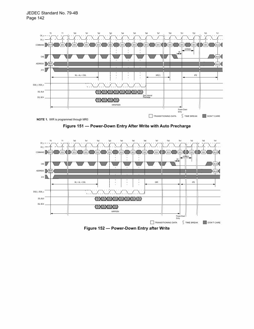
JEDEC Standard No. 79-4BPage 142
Figure 151 — Power-Down Entry After Write with Auto Precharge
Figure 152 — Power-Down Entry after Write
b+2
DES
Ta0 Ta1 Ta3 Ta4 Ta5 Ta6Ta2 Ta7 Tb0 Tb1 Tb2
DES DES DES
tWRAPDEN
DIN
bDIN
b+1DIN DIN
b+3DIN
b+4DIN
b+5DIN
b+6DIN
b+7
DIN
nDIN
n+2DIN
n+3DIN
n+1
WL = AL + CWL
T1T0
DES
CK_c
CK_t
COMMAND
ADDRESS
DQS_t, DQS_c
DQ, BL8
tCPDED
tIS
CKE
Bank,
WR(1)
DQ, BC4
Power-DownEntry
TIME BREAK DON’T CARETRANSITIONING DATA
Tc0 Tc1
DES DES
VALID
VALIDCol n
Start InternalPrecharge
tPD
A10
NOTE 1. tWR is programmed through MR0.
WRITE DES DES DES DES DES DES VALID
b+2
DES
Ta0 Ta1 Ta3 Ta4 Ta5 Ta6Ta2 Ta7 Tb0 Tb1 Tc0
DES DES DES
tWRPDEN
DIN
bDIN
b+1DIN DIN
b+3DIN
b+4DIN
b+5DIN
b+6DIN
b+7
DIN
nDIN
n+2DIN
n+3DIN
n+1
WL = AL + CWL
T1T0
DES
CK_c
CK_t
COMMAND
ADDRESS
DQS_t, DQS_c
DQ, BL8
tIS
CKE
Bank,
tWR
DQ, BC4
Power-DownEntry
TIME BREAK DON’T CARETRANSITIONING DATA
Td0 Td1
DES DES
VALID
VALIDCol n
tPD
A10
DES DES DES DES DES DES VALIDWRITE
tCPDED
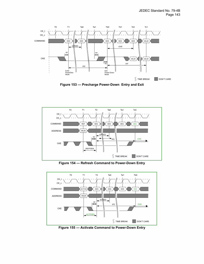
JEDEC Standard No. 79-4B Page 143
Figure 153 — Precharge Power-Down Entry and Exit
Figure 154 — Refresh Command to Power-Down Entry
Figure 155 — Activate Command to Power-Down Entry
DES
CK_t
CK_c
COMMAND
CKE
T0 T1 Ta0 Ta1 Tb0 Tb1 Tc0 Tc1
DES DES DES DES
tIS tIH
VALID DES VALID
tIS tXP
tPD
tCKE
DES DES VALIDDES DES
TIME BREAK DON’T CARE
EnterPowerDwnMode
ExitPower-DownMode
tCPDED
DES
CK_t
CK_c
COMMAND
CKE
T0 T1 T2 Ta0 Ta1 Tc0
DES DES
tIStPD
REF DES
TIME BREAK DON’T CARE
DES
VALIDADDRESS
DES DES DES
tREFPDEN
tCPDED
tCKE
DES
CK_t
CK_c
COMMAND
CKE
T0 T1 T2 Ta0 Ta1 Tb0
DES DES
tIStPD
ACTIVE DES
TIME BREAK DON’T CARE
DES
VALIDADDRESS
DES DES DES
tCPDED
tACTPDEN
tCKE
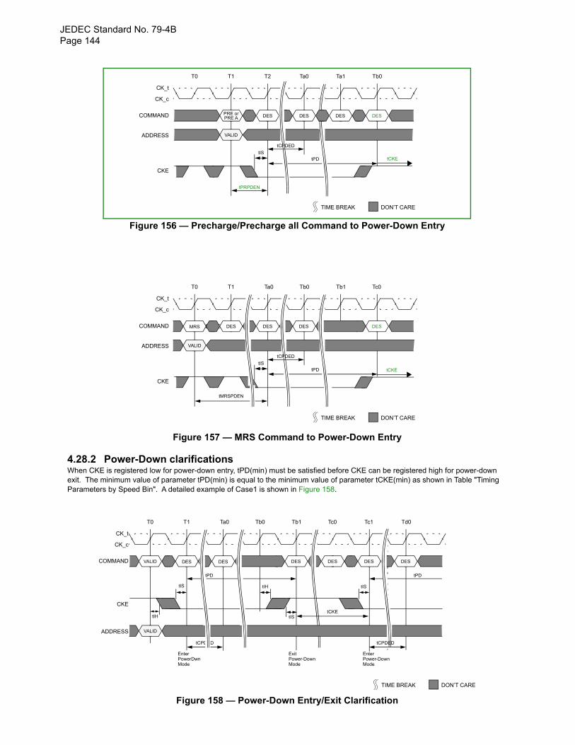
JEDEC Standard No. 79-4BPage 144
Figure 156 — Precharge/Precharge all Command to Power-Down Entry
Figure 157 — MRS Command to Power-Down Entry
4.28.2 Power-Down clarificationsWhen CKE is registered low for power-down entry, tPD(min) must be satisfied before CKE can be registered high for power-down exit. The minimum value of parameter tPD(min) is equal to the minimum value of parameter tCKE(min) as shown in Table "TimingParameters by Speed Bin". A detailed example of Case1 is shown in Figure 158.
Figure 158 — Power-Down Entry/Exit Clarification
DES
CK_t
CK_c
COMMAND
CKE
T0 T1 T2 Ta0 Ta1 Tb0
DES DES
tIStPD
PRE or DES
TIME BREAK DON’T CARE
DES
VALIDADDRESS
DES DES DESPRE A
tCPDED
tPRPDEN
tCKE
DESDES
CK_t
CK_c
COMMAND
CKE
T0 T1 Ta0 Tb0 Tb1 Tc0
DES
tIStPD
DES
TIME BREAK DON’T CARE
DES
ADDRESS
DES DES DES
tMRSPDEN
MRS
VALID
tCPDED
tCKE
DES
CK_t
CK_c
COMMAND
CKE
T0 T1 Ta0 Tb0 Tb1 Tc0 Tc1 Td0
DES DES DES DES
tIS tIH
tIStCKE
tCPDED
DES DES DESVALID DES
TIME BREAK DON’T CARE
EnterPowerDwnMode
ExitPower-DownMode
DESDES
tPD
tIH
VALID
tIS
EnterPower-DownMode
ADDRESS
tCPDED
tPD
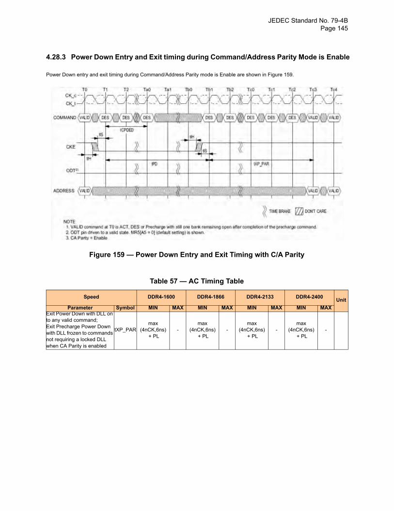
JEDEC Standard No. 79-4B Page 145
4.28.3 Power Down Entry and Exit timing during Command/Address Parity Mode is Enable Power Down entry and exit timing during Command/Address Parity mode is Enable are shown in Figure 159.
Figure 159 — Power Down Entry and Exit Timing with C/A Parity
Table 57 — AC Timing Table
Speed DDR4-1600 DDR4-1866 DDR4-2133 DDR4-2400Unit
Parameter Symbol MIN MAX MIN MAX MIN MAX MIN MAXExit Power Down with DLL on to any valid command;Exit Precharge Power Down with DLL frozen to commands not requiring a locked DLL when CA Parity is enabled
tXP_PARmax
(4nCK,6ns) + PL
-max
(4nCK,6ns) + PL
-max
(4nCK,6ns) + PL
-max
(4nCK,6ns) + PL
-
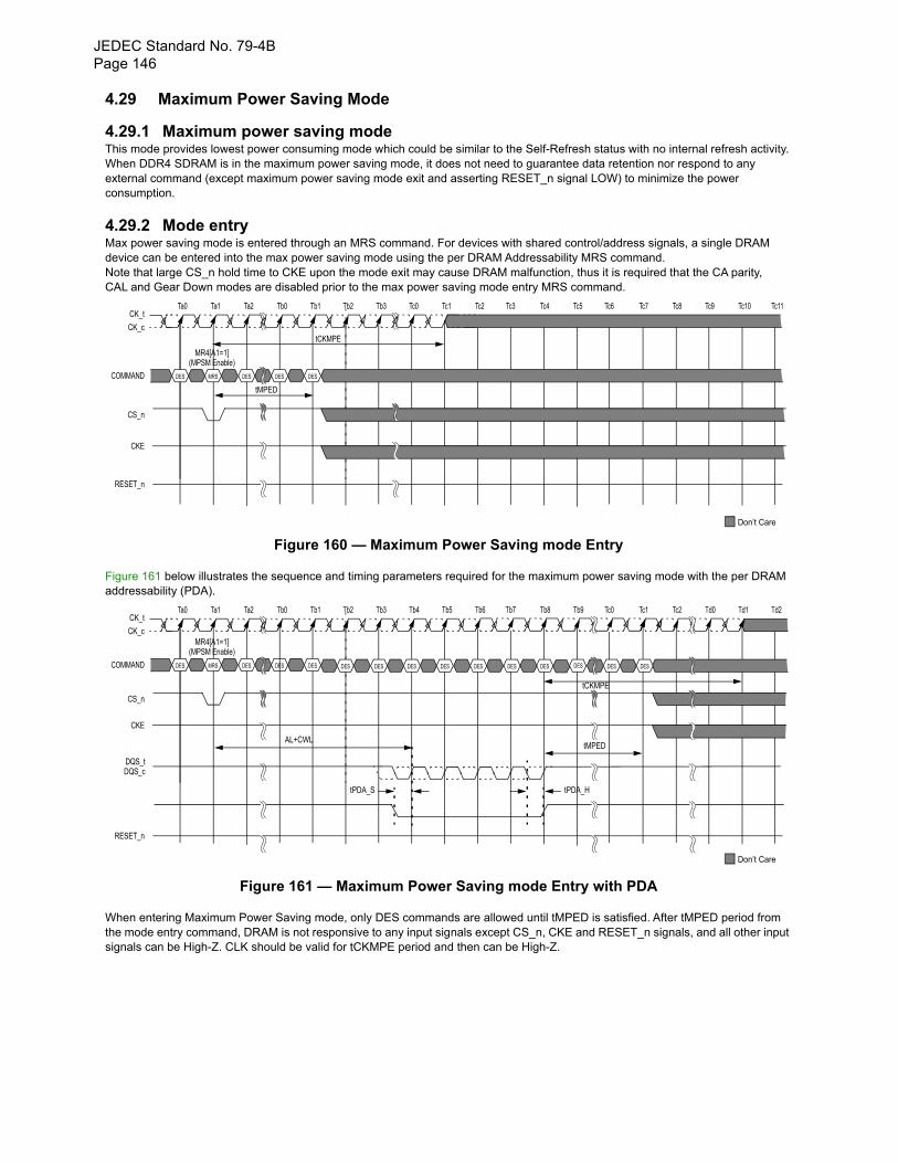
JEDEC Standard No. 79-4BPage 146
4.29 Maximum Power Saving Mode
4.29.1 Maximum power saving modeThis mode provides lowest power consuming mode which could be similar to the Self-Refresh status with no internal refresh activity. When DDR4 SDRAM is in the maximum power saving mode, it does not need to guarantee data retention nor respond to any external command (except maximum power saving mode exit and asserting RESET_n signal LOW) to minimize the power consumption.
4.29.2 Mode entryMax power saving mode is entered through an MRS command. For devices with shared control/address signals, a single DRAM device can be entered into the max power saving mode using the per DRAM Addressability MRS command.Note that large CS_n hold time to CKE upon the mode exit may cause DRAM malfunction, thus it is required that the CA parity, CAL and Gear Down modes are disabled prior to the max power saving mode entry MRS command.
Figure 160 — Maximum Power Saving mode Entry
Figure 161 below illustrates the sequence and timing parameters required for the maximum power saving mode with the per DRAM addressability (PDA).
Figure 161 — Maximum Power Saving mode Entry with PDA
When entering Maximum Power Saving mode, only DES commands are allowed until tMPED is satisfied. After tMPED period from the mode entry command, DRAM is not responsive to any input signals except CS_n, CKE and RESET_n signals, and all other input signals can be High-Z. CLK should be valid for tCKMPE period and then can be High-Z.
Ta2 Tb0 Tb2 Tb3 Tc0 Tc1Tb1 Tc2 Tc3 Tc4 Tc5Ta1Ta0CK_t
COMMAND
RESET_n
CS_n
Tc6 Tc7
CKE
DESDES
Tc8 Tc9 Tc10 Tc11
tCKMPE
MR4[A1=1](MPSM Enable)
tMPED
Don’t Care
CK_c
DES DESMRS
Ta2 Tb0 Tb2 Tb3 Tb4 Tb5Tb1 Tb6 Tb7 Tb8 Tb9
DES
Ta1Ta0
MRS
CK_t
COMMAND
RESET_n
CS_n
Tc0 Tc1
CKE
DESDES
Tc2 Td0 Td1 Td2
MR4[A1=1](MPSM Enable)
tCKMPE
Don’t Care
CK_c
DES DESDES DES DES DESDES DES DES DES
AL+CWLtMPED
DQS_tDQS_c
tPDA_S tPDA_H
DES
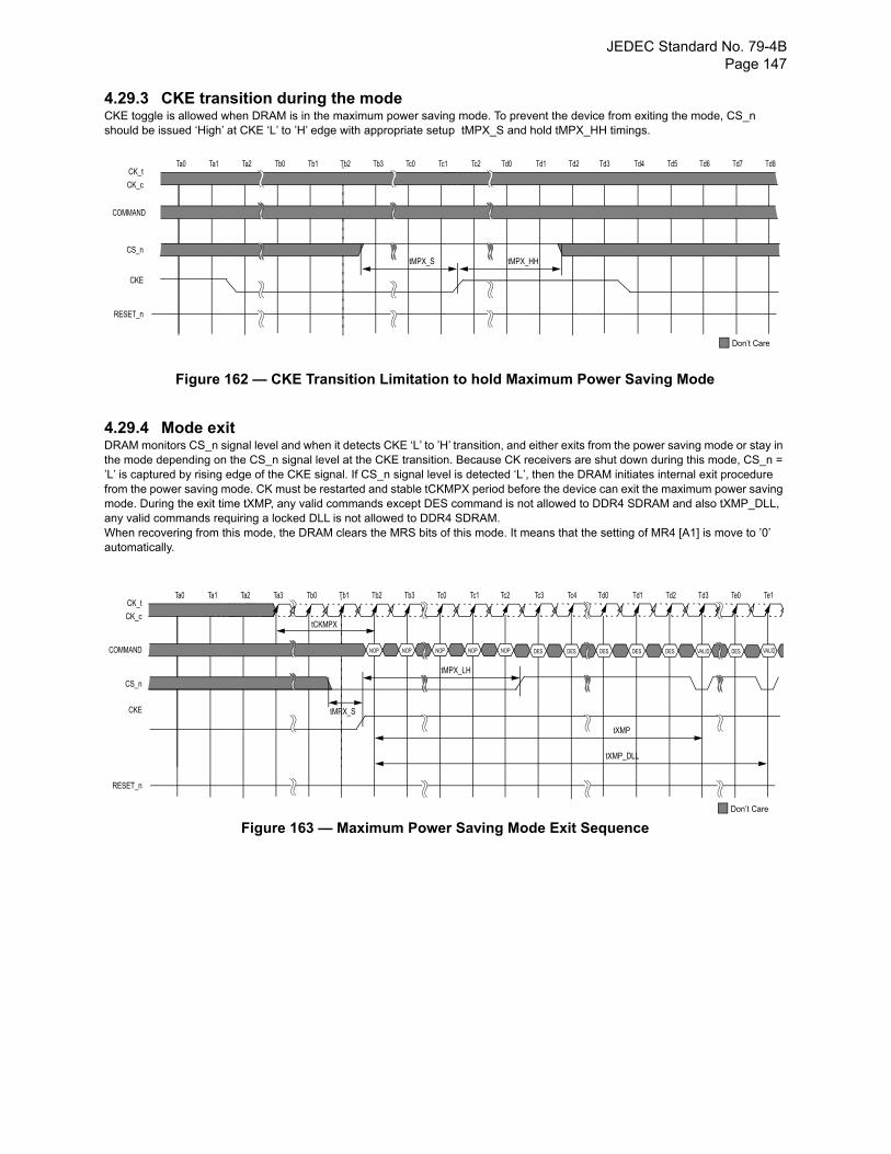
JEDEC Standard No. 79-4B Page 147
4.29.3 CKE transition during the modeCKE toggle is allowed when DRAM is in the maximum power saving mode. To prevent the device from exiting the mode, CS_n should be issued ‘High’ at CKE ‘L’ to ’H’ edge with appropriate setup tMPX_S and hold tMPX_HH timings.
Figure 162 — CKE Transition Limitation to hold Maximum Power Saving Mode
4.29.4 Mode exitDRAM monitors CS_n signal level and when it detects CKE ‘L’ to ’H’ transition, and either exits from the power saving mode or stay in the mode depending on the CS_n signal level at the CKE transition. Because CK receivers are shut down during this mode, CS_n = ’L’ is captured by rising edge of the CKE signal. If CS_n signal level is detected ‘L’, then the DRAM initiates internal exit procedure from the power saving mode. CK must be restarted and stable tCKMPX period before the device can exit the maximum power saving mode. During the exit time tXMP, any valid commands except DES command is not allowed to DDR4 SDRAM and also tXMP_DLL, any valid commands requiring a locked DLL is not allowed to DDR4 SDRAM.When recovering from this mode, the DRAM clears the MRS bits of this mode. It means that the setting of MR4 [A1] is move to ’0’ automatically.
Figure 163 — Maximum Power Saving Mode Exit Sequence
Ta2 Tb0 Tb2 Tb3 Tc0 Tc1Tb1 Tc2 Td0 Td1 Td2Ta1Ta0CK_t
COMMAND
RESET_n
CS_n
Td3 Td4
CKE
Td5 Td6 Td7 Td8
Don’t Care
CK_c
tMPX_S tMPX_HH
NOP
Ta2 Ta3 Tb1 Tb2 Tb3 Tc0Tb0 Tc1 Tc2 Tc3 Tc4
NOP
Ta1Ta0
NOP
CK_t
COMMAND
RESET_n
CS_n
Td0 Td1
CKE
NOPNOP
Td2 Td3 Te0 Te1
tCKMPX
Don’t Care
CK_c
DES DESDES DES VALID DESDES VALID
tMPX_S
tMPX_LH
tXMP
tXMP_DLL
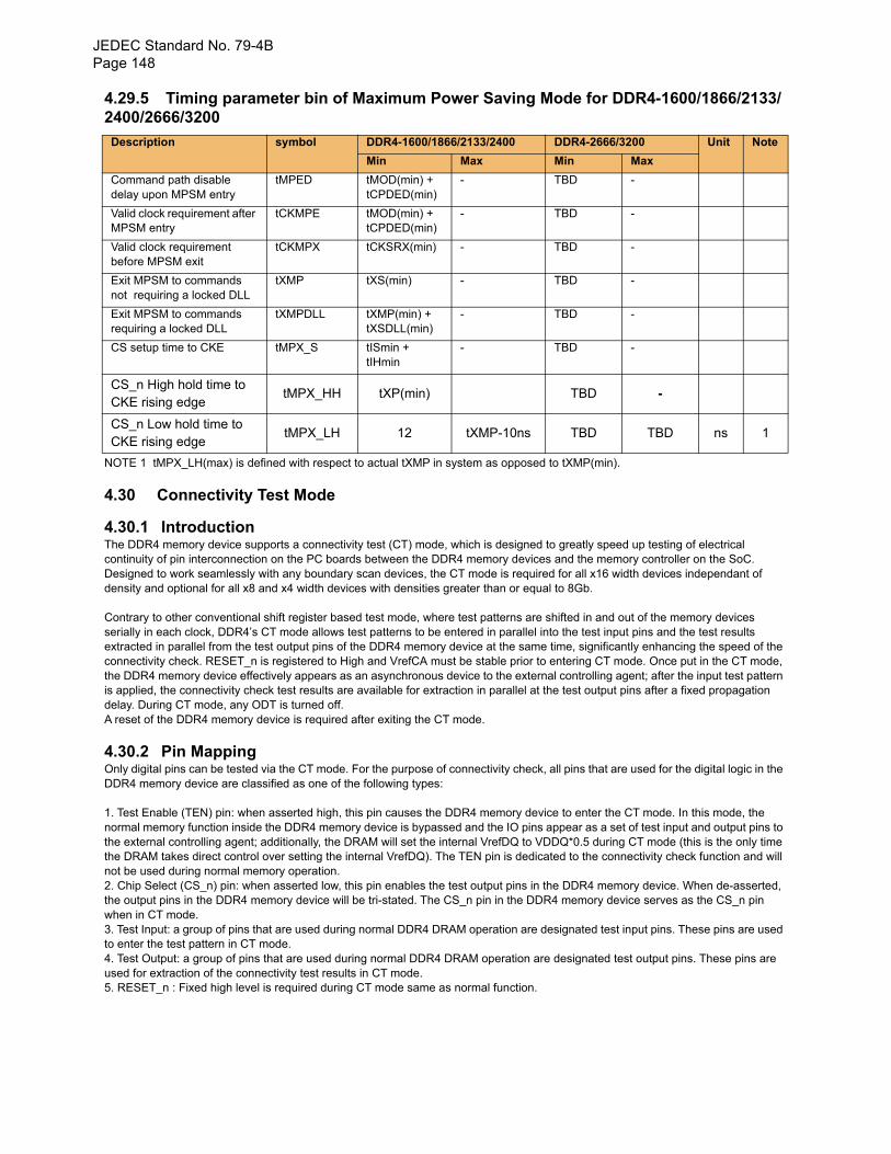
JEDEC Standard No. 79-4BPage 148
4.29.5 Timing parameter bin of Maximum Power Saving Mode for DDR4-1600/1866/2133/2400/2666/3200
NOTE 1 tMPX_LH(max) is defined with respect to actual tXMP in system as opposed to tXMP(min).
4.30 Connectivity Test Mode
4.30.1 IntroductionThe DDR4 memory device supports a connectivity test (CT) mode, which is designed to greatly speed up testing of electrical continuity of pin interconnection on the PC boards between the DDR4 memory devices and the memory controller on the SoC. Designed to work seamlessly with any boundary scan devices, the CT mode is required for all x16 width devices independant of density and optional for all x8 and x4 width devices with densities greater than or equal to 8Gb.
Contrary to other conventional shift register based test mode, where test patterns are shifted in and out of the memory devices serially in each clock, DDR4’s CT mode allows test patterns to be entered in parallel into the test input pins and the test results extracted in parallel from the test output pins of the DDR4 memory device at the same time, significantly enhancing the speed of the connectivity check. RESET_n is registered to High and VrefCA must be stable prior to entering CT mode. Once put in the CT mode, the DDR4 memory device effectively appears as an asynchronous device to the external controlling agent; after the input test pattern is applied, the connectivity check test results are available for extraction in parallel at the test output pins after a fixed propagation delay. During CT mode, any ODT is turned off.A reset of the DDR4 memory device is required after exiting the CT mode.
4.30.2 Pin MappingOnly digital pins can be tested via the CT mode. For the purpose of connectivity check, all pins that are used for the digital logic in the DDR4 memory device are classified as one of the following types:
1. Test Enable (TEN) pin: when asserted high, this pin causes the DDR4 memory device to enter the CT mode. In this mode, the normal memory function inside the DDR4 memory device is bypassed and the IO pins appear as a set of test input and output pins to the external controlling agent; additionally, the DRAM will set the internal VrefDQ to VDDQ*0.5 during CT mode (this is the only time the DRAM takes direct control over setting the internal VrefDQ). The TEN pin is dedicated to the connectivity check function and will not be used during normal memory operation.2. Chip Select (CS_n) pin: when asserted low, this pin enables the test output pins in the DDR4 memory device. When de-asserted, the output pins in the DDR4 memory device will be tri-stated. The CS_n pin in the DDR4 memory device serves as the CS_n pin when in CT mode.3. Test Input: a group of pins that are used during normal DDR4 DRAM operation are designated test input pins. These pins are used to enter the test pattern in CT mode.4. Test Output: a group of pins that are used during normal DDR4 DRAM operation are designated test output pins. These pins are used for extraction of the connectivity test results in CT mode.5. RESET_n : Fixed high level is required during CT mode same as normal function.
Description symbol DDR4-1600/1866/2133/2400 DDR4-2666/3200 Unit Note
Min Max Min Max
Command path disable delay upon MPSM entry
tMPED tMOD(min) + tCPDED(min)
- TBD -
Valid clock requirement after MPSM entry
tCKMPE tMOD(min) + tCPDED(min)
- TBD -
Valid clock requirement before MPSM exit
tCKMPX tCKSRX(min) - TBD -
Exit MPSM to commands not requiring a locked DLL
tXMP tXS(min) - TBD -
Exit MPSM to commands requiring a locked DLL
tXMPDLL tXMP(min) + tXSDLL(min)
- TBD -
CS setup time to CKE tMPX_S tISmin + tIHmin
- TBD -
CS_n High hold time to CKE rising edge
tMPX_HH tXP(min) TBD -
CS_n Low hold time to CKE rising edge
tMPX_LH 12 tXMP-10ns TBD TBD ns 1
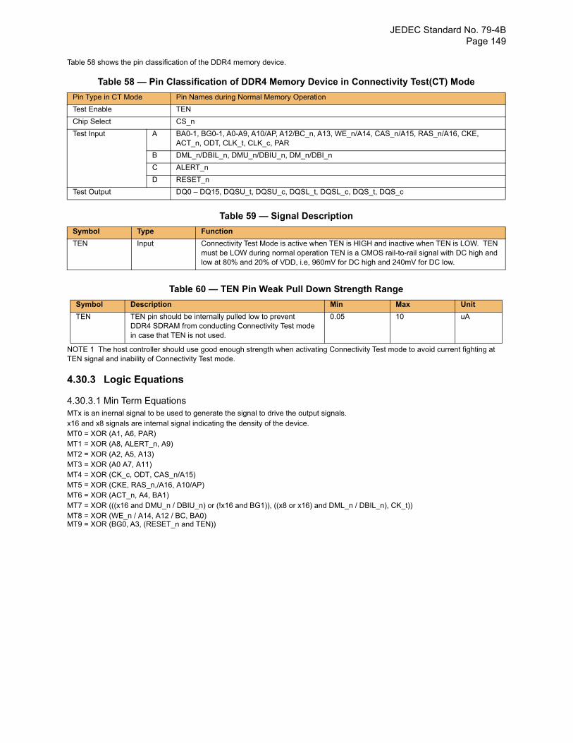
JEDEC Standard No. 79-4B Page 149
Table 58 shows the pin classification of the DDR4 memory device.
Table 58 — Pin Classification of DDR4 Memory Device in Connectivity Test(CT) Mode
Table 59 — Signal Description
Table 60 — TEN Pin Weak Pull Down Strength Range
NOTE 1 The host controller should use good enough strength when activating Connectivity Test mode to avoid current fighting at TEN signal and inability of Connectivity Test mode.
4.30.3 Logic Equations
4.30.3.1 Min Term EquationsMTx is an inernal signal to be used to generate the signal to drive the output signals.x16 and x8 signals are internal signal indicating the density of the device.MT0 = XOR (A1, A6, PAR)MT1 = XOR (A8, ALERT_n, A9)MT2 = XOR (A2, A5, A13)MT3 = XOR (A0 A7, A11)MT4 = XOR (CK_c, ODT, CAS_n/A15)MT5 = XOR (CKE, RAS_n,/A16, A10/AP)MT6 = XOR (ACT_n, A4, BA1)MT7 = XOR (((x16 and DMU_n / DBIU_n) or (!x16 and BG1)), ((x8 or x16) and DML_n / DBIL_n), CK_t))MT8 = XOR (WE_n / A14, A12 / BC, BA0)MT9 = XOR (BG0, A3, (RESET_n and TEN))
Pin Type in CT Mode Pin Names during Normal Memory Operation
Test Enable TEN
Chip Select CS_n
Test Input A BA0-1, BG0-1, A0-A9, A10/AP, A12/BC_n, A13, WE_n/A14, CAS_n/A15, RAS_n/A16, CKE, ACT_n, ODT, CLK_t, CLK_c, PAR
B DML_n/DBIL_n, DMU_n/DBIU_n, DM_n/DBI_n
C ALERT_n
D RESET_n
Test Output DQ0 – DQ15, DQSU_t, DQSU_c, DQSL_t, DQSL_c, DQS_t, DQS_c
Symbol Type Function
TEN Input Connectivity Test Mode is active when TEN is HIGH and inactive when TEN is LOW. TEN must be LOW during normal operation TEN is a CMOS rail-to-rail signal with DC high and low at 80% and 20% of VDD, i.e, 960mV for DC high and 240mV for DC low.
Symbol Description Min Max Unit
TEN TEN pin should be internally pulled low to preventDDR4 SDRAM from conducting Connectivity Test mode in case that TEN is not used.
0.05 10 uA
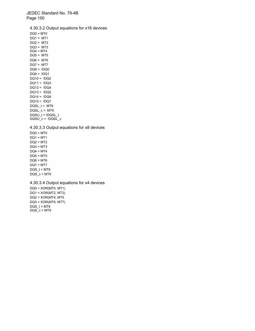
JEDEC Standard No. 79-4BPage 150
4.30.3.2 Output equations for x16 devicesDQ0 = MT0DQ1 = MT1DQ2 = MT2DQ3 = MT3DQ4 = MT4DQ5 = MT5
DQ6 = MT6DQ7 = MT7DQ8 = !DQ0DQ9 = !DQ1DQ10 = !DQ2DQ11 = !DQ3DQ12 = !DQ4DQ13 = !DQ5DQ14 = !DQ6DQ15 = !DQ7DQSL_t = MT8DQSL_c = MT9DQSU_t = !DQSL_tDQSU_c = !DQSL_c
4.30.3.3 Output equations for x8 devicesDQ0 = MT0DQ1 = MT1DQ2 = MT2DQ3 = MT3DQ4 = MT4DQ5 = MT5DQ6 = MT6DQ7 = MT7DQS_t = MT8DQS_c = MT9
4.30.3.4 Output equations for x4 devicesDQ0 = XOR(MT0, MT1)DQ1 = XOR(MT2, MT3)DQ2 = XOR(MT4, MT5DQ3 = XOR(MT6, MT7)DQS_t = MT8DQS_c = MT9
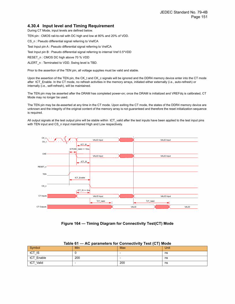
JEDEC Standard No. 79-4B Page 151
4.30.4 Input level and Timing Requirement During CT Mode, input levels are defined below.
TEN pin : CMOS rail-to-rail with DC high and low at 80% and 20% of VDD.
CS_n : Pseudo differential signal referring to VrefCA
Test Input pin A : Pseudo differential signal referring to VrefCA
Test Input pin B : Pseudo differential signal referring to internal Vref 0.5*VDD
RESET_n : CMOS DC high above 70 % VDD
ALERT_n : Terminated to VDD. Swing level is TBD.
Prior to the assertion of the TEN pin, all voltage supplies must be valid and stable.
Upon the assertion of the TEN pin, the CK_t and CK_c signals will be ignored and the DDR4 memory device enter into the CT mode after tCT_Enable. In the CT mode, no refresh activities in the memory arrays, initiated either externally (i.e., auto-refresh) or internally (i.e., self-refresh), will be maintained.
The TEN pin may be asserted after the DRAM has completed power-on; once the DRAM is initialized and VREFdq is calibrated, CT Mode may no longer be used.
The TEN pin may be de-asserted at any time in the CT mode. Upon exiting the CT mode, the states of the DDR4 memory device are unknown and the integrity of the original content of the memory array is not guaranteed and therefore the reset initialization sequence is required.
All output signals at the test output pins will be stable within tCT_valid after the test inputs have been applied to the test input pins with TEN input and CS_n input maintained High and Low respectively.
Figure 164 — Timing Diagram for Connectivity Test(CT) Mode
Table 61 — AC parameters for Connectivity Test (CT) Mode Symbol Min Max Unit
tCT_IS 0 - ns
tCT_Enable 200 - ns
tCT_Valid - 200 ns
CK_c
CK_t
CKE
RESET_n
TEN
CT Outputs
tCTCKE_Valid >= 10ns
VALID Input VALID Input
VALID Input VALID Input
tCT_Enable
tCT_IS >= 0ns
VALID Input VALID Input
CS_n
CT Inputs
VALID VALID
tCT_ValidtCT_Valid
tCT_IS
tCT_IS
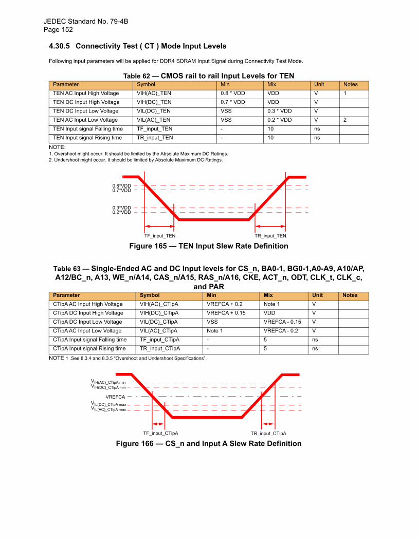
JEDEC Standard No. 79-4BPage 152
4.30.5 Connectivity Test ( CT ) Mode Input Levels
Following input parameters will be applied for DDR4 SDRAM Input Signal during Connectivity Test Mode.
Table 62 — CMOS rail to rail Input Levels for TEN
NOTE:1. Overshoot might occur. It should be limited by the Absolute Maximum DC Ratings.2. Undershoot might occur. It should be limited by Absolute Maximum DC Ratings.
Figure 165 — TEN Input Slew Rate Definition
Table 63 — Single-Ended AC and DC Input levels for CS_n, BA0-1, BG0-1,A0-A9, A10/AP, A12/BC_n, A13, WE_n/A14, CAS_n/A15, RAS_n/A16, CKE, ACT_n, ODT, CLK_t, CLK_c,
and PAR
NOTE 1 .See 8.3.4 and 8.3.5 “Overshoot and Undershoot Specifications”.
Figure 166 — CS_n and Input A Slew Rate Definition
Parameter Symbol Min Mix Unit Notes
TEN AC Input High Voltage VIH(AC)_TEN 0.8 * VDD VDD V 1
TEN DC Input High Voltage VIH(DC)_TEN 0.7 * VDD VDD V
TEN DC Input Low Voltage VIL(DC)_TEN VSS 0.3 * VDD V
TEN AC Input Low Voltage VIL(AC)_TEN VSS 0.2 * VDD V 2
TEN Input signal Falling time TF_input_TEN - 10 ns
TEN Input signal Rising time TR_input_TEN - 10 ns
Parameter Symbol Min Mix Unit Notes
CTipA AC Input High Voltage VIH(AC)_CTipA VREFCA + 0.2 Note 1 V
CTipA DC Input High Voltage VIH(DC)_CTipA VREFCA + 0.15 VDD V
CTipA DC Input Low Voltage VIL(DC)_CTipA VSS VREFCA - 0.15 V
CTipA AC Input Low Voltage VIL(AC)_CTipA Note 1 VREFCA - 0.2 V
CTipA Input signal Falling time TF_input_CTipA - 5 ns
CTipA Input signal Rising time TR_input_CTipA - 5 ns
0.8*VDD
TR_input_TENTF_input_TEN
0.7*VDD
0.3*VDD 0.2*VDD
VIH(AC)_CTipA min
TR_input_CTipA TF_input_CTipA
VREFCA
VIH(DC)_CTipA min
VIL(DC)_CTipA max VIL(AC)_CTipA max
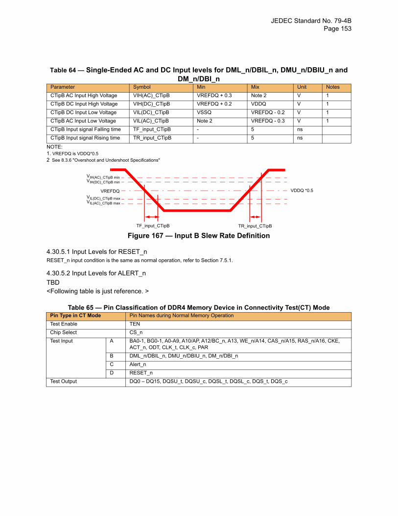
JEDEC Standard No. 79-4B Page 153
Table 64 — Single-Ended AC and DC Input levels for DML_n/DBIL_n, DMU_n/DBIU_n and DM_n/DBI_n
NOTE:1. VREFDQ is VDDQ*0.5
2 See 8.3.6 "Overshoot and Undershoot Specifications"
Figure 167 — Input B Slew Rate Definition
4.30.5.1 Input Levels for RESET_nRESET_n input condition is the same as normal operation, refer to Section 7.5.1.
4.30.5.2 Input Levels for ALERT_n
TBD<Following table is just reference. >
Table 65 — Pin Classification of DDR4 Memory Device in Connectivity Test(CT) Mode
Parameter Symbol Min Mix Unit Notes
CTipB AC Input High Voltage VIH(AC)_CTipB VREFDQ + 0.3 Note 2 V 1
CTipB DC Input High Voltage VIH(DC)_CTipB VREFDQ + 0.2 VDDQ V 1
CTipB DC Input Low Voltage VIL(DC)_CTipB VSSQ VREFDQ - 0.2 V 1
CTipB AC Input Low Voltage VIL(AC)_CTipB Note 2 VREFDQ - 0.3 V 1
CTipB Input signal Falling time TF_input_CTipB - 5 ns
CTipB Input signal Rising time TR_input_CTipB - 5 ns
Pin Type in CT Mode Pin Names during Normal Memory Operation
Test Enable TEN
Chip Select CS_n
Test Input A BA0-1, BG0-1, A0-A9, A10/AP, A12/BC_n, A13, WE_n/A14, CAS_n/A15, RAS_n/A16, CKE, ACT_n, ODT, CLK_t, CLK_c, PAR
B DML_n/DBIL_n, DMU_n/DBIU_n, DM_n/DBI_n
C Alert_n
D RESET_n
Test Output DQ0 – DQ15, DQSU_t, DQSU_c, DQSL_t, DQSL_c, DQS_t, DQS_c
VIH(AC)_CTipB min
TR_input_CTipB TF_input_CTipB
VREFDQ
VIH(DC)_CTipB min
VIL(DC)_CTipB max VIL(AC)_CTipB max
VDDQ *0.5
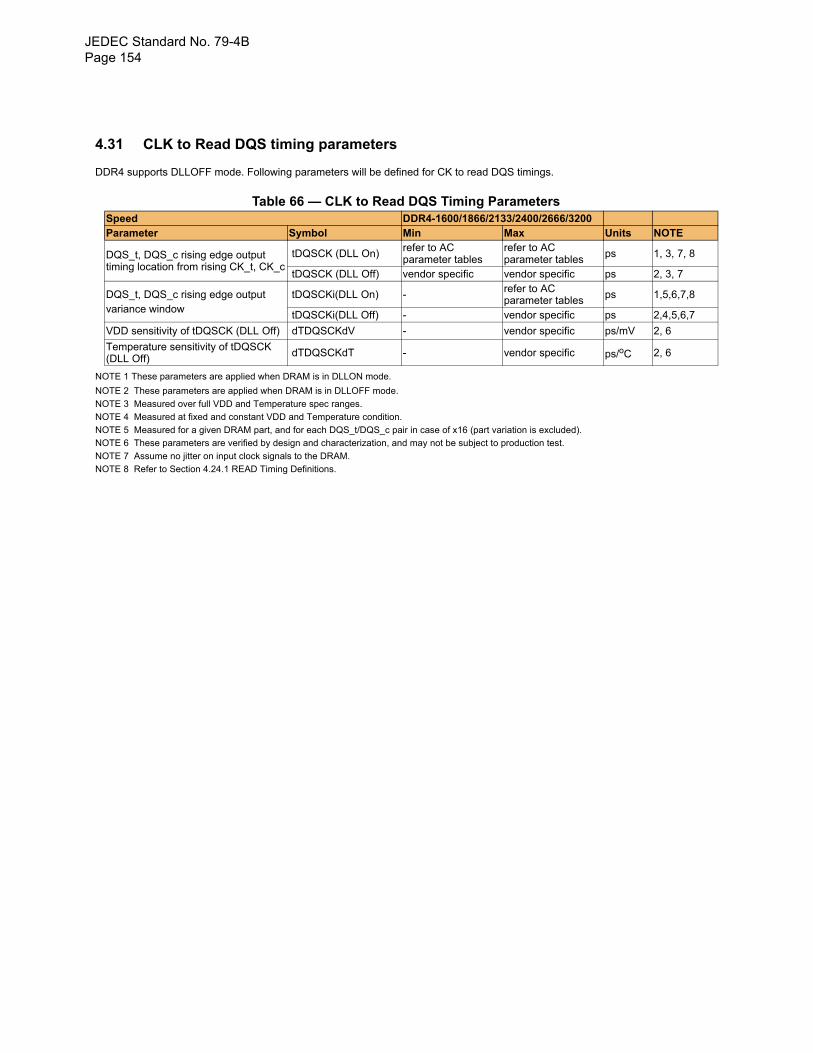
JEDEC Standard No. 79-4BPage 154
4.31 CLK to Read DQS timing parameters
DDR4 supports DLLOFF mode. Following parameters will be defined for CK to read DQS timings.
Table 66 — CLK to Read DQS Timing Parameters
NOTE 1 These parameters are applied when DRAM is in DLLON mode.
NOTE 2 These parameters are applied when DRAM is in DLLOFF mode.
NOTE 3 Measured over full VDD and Temperature spec ranges.
NOTE 4 Measured at fixed and constant VDD and Temperature condition.
NOTE 5 Measured for a given DRAM part, and for each DQS_t/DQS_c pair in case of x16 (part variation is excluded).
NOTE 6 These parameters are verified by design and characterization, and may not be subject to production test.
NOTE 7 Assume no jitter on input clock signals to the DRAM.
NOTE 8 Refer to Section 4.24.1 READ Timing Definitions.
Speed DDR4-1600/1866/2133/2400/2666/3200Parameter Symbol Min Max Units NOTE
DQS_t, DQS_c rising edge output timing location from rising CK_t, CK_c
tDQSCK (DLL On)refer to AC parameter tables
refer to AC parameter tables ps 1, 3, 7, 8
tDQSCK (DLL Off) vendor specific vendor specific ps 2, 3, 7
DQS_t, DQS_c rising edge outputvariance window
tDQSCKi(DLL On) - refer to AC parameter tables ps 1,5,6,7,8
tDQSCKi(DLL Off) - vendor specific ps 2,4,5,6,7
VDD sensitivity of tDQSCK (DLL Off) dTDQSCKdV - vendor specific ps/mV 2, 6
Temperature sensitivity of tDQSCK (DLL Off) dTDQSCKdT - vendor specific ps/oC 2, 6
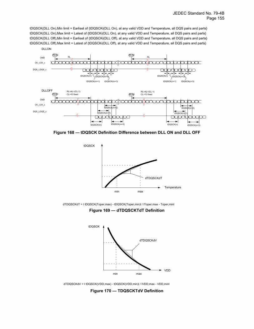
JEDEC Standard No. 79-4B Page 155
tDQSCK(DLL On),Min limit = Earliset of {tDQSCKi(DLL On), at any valid VDD and Temperature, all DQS pairs and parts}
tDQSCK(DLL On),Max limit = Latest of {tDQSCKi(DLL On), at any valid VDD and Temperature, all DQS pairs and parts}
tDQSCK(DLL Off),Min limit = Earliset of {tDQSCKi(DLL Off), at any valid VDD and Temperature, all DQS pairs and parts}
tDQSCK(DLL Off),Max limit = Latest of {tDQSCKi(DLL Off), at any valid VDD and Temperature, all DQS pairs and parts}
Figure 168 — tDQSCK Definition Difference between DLL ON and DLL OFF
Figure 169 — dTDQSCKTdT Definition
Figure 170 — TDQSCKTdV Definition
CMD
CK_t,CK_c
DQS_t,DQS_c
READRL
READRL
tDQSCK(m)
tDQSCK(m+1) tDQSCK(m+3)
tDQSCK(m+2) tDQSCK(n)
tDQSCK(n+1) tDQSCK(n+3)
tDQSCK(n+2)
DLLON
DLLOFF
CMD
CK_t,CK_c
DQS_t,DQS_c
READ READ
tDQSCK(m+2) tDQSCK(n+2)
tDQSCK(m+1) tDQSCK(n+1)
tDQSCK(m) tDQSCK(m+3) tDQSCK(n) tDQSCK(n+3)
RL=AL+(CL-1)
CL=10 fixedRL=AL+(CL-1)CL=10 fixed
tDQSCK
Temperature
min max
dTDQSCKdT
dTDQSCKdT = l tDQSCK(Toper,max) - tDQSCK(Toper,min)l / lToper,max - Toper,minl
tDQSCK
VDD
dTDQSCKdV
min max
dTDQSCKdV = l tDQSCK(VDD,max) - tDQSCK(VDD,min)l / lVDD,max - VDD,minl
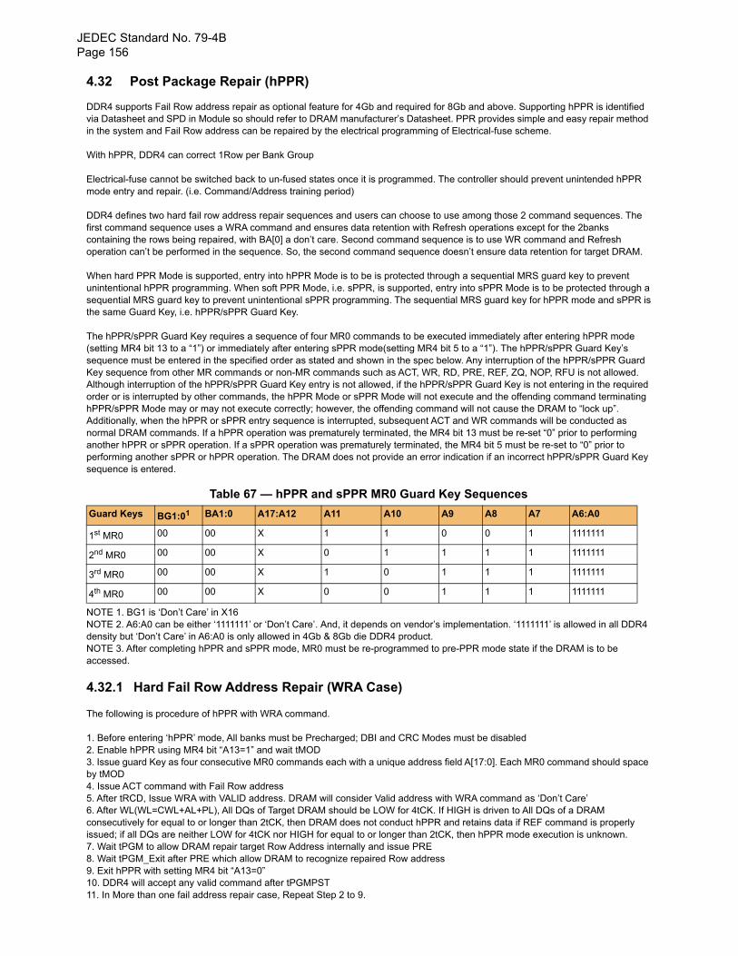
JEDEC Standard No. 79-4BPage 156
4.32 Post Package Repair (hPPR)
DDR4 supports Fail Row address repair as optional feature for 4Gb and required for 8Gb and above. Supporting hPPR is identified via Datasheet and SPD in Module so should refer to DRAM manufacturer’s Datasheet. PPR provides simple and easy repair method in the system and Fail Row address can be repaired by the electrical programming of Electrical-fuse scheme.
With hPPR, DDR4 can correct 1Row per Bank Group
Electrical-fuse cannot be switched back to un-fused states once it is programmed. The controller should prevent unintended hPPR mode entry and repair. (i.e. Command/Address training period)
DDR4 defines two hard fail row address repair sequences and users can choose to use among those 2 command sequences. The first command sequence uses a WRA command and ensures data retention with Refresh operations except for the 2banks containing the rows being repaired, with BA[0] a don’t care. Second command sequence is to use WR command and Refresh operation can’t be performed in the sequence. So, the second command sequence doesn’t ensure data retention for target DRAM.
When hard PPR Mode is supported, entry into hPPR Mode is to be is protected through a sequential MRS guard key to preventunintentional hPPR programming. When soft PPR Mode, i.e. sPPR, is supported, entry into sPPR Mode is to be protected through asequential MRS guard key to prevent unintentional sPPR programming. The sequential MRS guard key for hPPR mode and sPPR isthe same Guard Key, i.e. hPPR/sPPR Guard Key.
The hPPR/sPPR Guard Key requires a sequence of four MR0 commands to be executed immediately after entering hPPR mode (setting MR4 bit 13 to a “1”) or immediately after entering sPPR mode(setting MR4 bit 5 to a “1”). The hPPR/sPPR Guard Key’ssequence must be entered in the specified order as stated and shown in the spec below. Any interruption of the hPPR/sPPR GuardKey sequence from other MR commands or non-MR commands such as ACT, WR, RD, PRE, REF, ZQ, NOP, RFU is not allowed.Although interruption of the hPPR/sPPR Guard Key entry is not allowed, if the hPPR/sPPR Guard Key is not entering in the required order or is interrupted by other commands, the hPPR Mode or sPPR Mode will not execute and the offending command terminating hPPR/sPPR Mode may or may not execute correctly; however, the offending command will not cause the DRAM to “lock up”. Additionally, when the hPPR or sPPR entry sequence is interrupted, subsequent ACT and WR commands will be conducted as normal DRAM commands. If a hPPR operation was prematurely terminated, the MR4 bit 13 must be re-set “0” prior to performing another hPPR or sPPR operation. If a sPPR operation was prematurely terminated, the MR4 bit 5 must be re-set to “0” prior to performing another sPPR or hPPR operation. The DRAM does not provide an error indication if an incorrect hPPR/sPPR Guard Key sequence is entered.
Table 67 — hPPR and sPPR MR0 Guard Key Sequences
NOTE 1. BG1 is ‘Don’t Care’ in X16NOTE 2. A6:A0 can be either ‘1111111’ or ‘Don’t Care’. And, it depends on vendor’s implementation. ‘1111111’ is allowed in all DDR4 density but ‘Don’t Care’ in A6:A0 is only allowed in 4Gb & 8Gb die DDR4 product.NOTE 3. After completing hPPR and sPPR mode, MR0 must be re-programmed to pre-PPR mode state if the DRAM is to be accessed.
4.32.1 Hard Fail Row Address Repair (WRA Case)
The following is procedure of hPPR with WRA command.
1. Before entering ‘hPPR’ mode, All banks must be Precharged; DBI and CRC Modes must be disabled2. Enable hPPR using MR4 bit “A13=1” and wait tMOD3. Issue guard Key as four consecutive MR0 commands each with a unique address field A[17:0]. Each MR0 command should space by tMOD4. Issue ACT command with Fail Row address5. After tRCD, Issue WRA with VALID address. DRAM will consider Valid address with WRA command as ‘Don’t Care’6. After WL(WL=CWL+AL+PL), All DQs of Target DRAM should be LOW for 4tCK. If HIGH is driven to All DQs of a DRAM consecutively for equal to or longer than 2tCK, then DRAM does not conduct hPPR and retains data if REF command is properly issued; if all DQs are neither LOW for 4tCK nor HIGH for equal to or longer than 2tCK, then hPPR mode execution is unknown.7. Wait tPGM to allow DRAM repair target Row Address internally and issue PRE 8. Wait tPGM_Exit after PRE which allow DRAM to recognize repaired Row address9. Exit hPPR with setting MR4 bit “A13=0” 10. DDR4 will accept any valid command after tPGMPST11. In More than one fail address repair case, Repeat Step 2 to 9.
Guard Keys BG1:01 BA1:0 A17:A12 A11 A10 A9 A8 A7 A6:A0
1st MR0 00 00 X 1 1 0 0 1 1111111
2nd MR0 00 00 X 0 1 1 1 1 1111111
3rd MR0 00 00 X 1 0 1 1 1 1111111
4th MR0 00 00 X 0 0 1 1 1 1111111
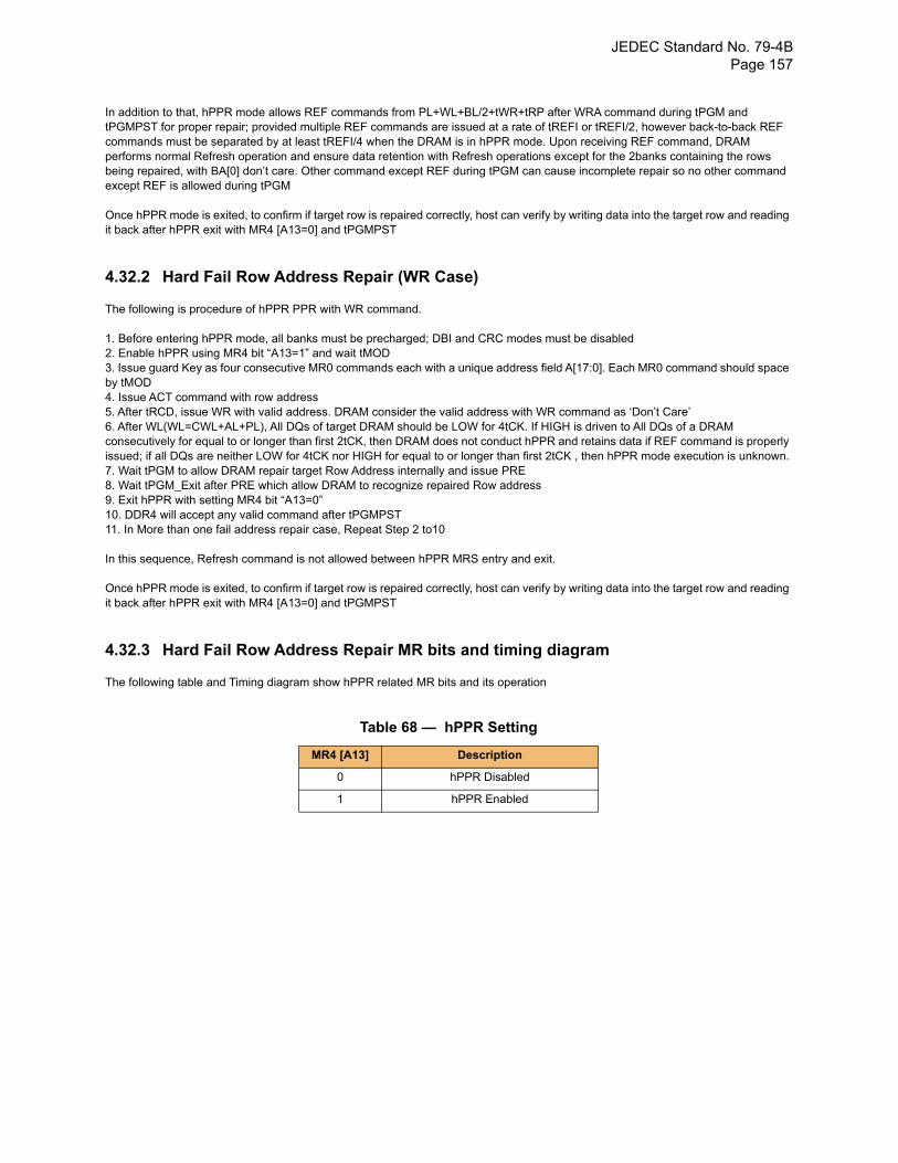
JEDEC Standard No. 79-4B Page 157
In addition to that, hPPR mode allows REF commands from PL+WL+BL/2+tWR+tRP after WRA command during tPGM and tPGMPST for proper repair; provided multiple REF commands are issued at a rate of tREFI or tREFI/2, however back-to-back REF commands must be separated by at least tREFI/4 when the DRAM is in hPPR mode. Upon receiving REF command, DRAM performs normal Refresh operation and ensure data retention with Refresh operations except for the 2banks containing the rows being repaired, with BA[0] don’t care. Other command except REF during tPGM can cause incomplete repair so no other command except REF is allowed during tPGM
Once hPPR mode is exited, to confirm if target row is repaired correctly, host can verify by writing data into the target row and reading it back after hPPR exit with MR4 [A13=0] and tPGMPST
4.32.2 Hard Fail Row Address Repair (WR Case)
The following is procedure of hPPR PPR with WR command.
1. Before entering hPPR mode, all banks must be precharged; DBI and CRC modes must be disabled2. Enable hPPR using MR4 bit “A13=1” and wait tMOD3. Issue guard Key as four consecutive MR0 commands each with a unique address field A[17:0]. Each MR0 command should space by tMOD4. Issue ACT command with row address5. After tRCD, issue WR with valid address. DRAM consider the valid address with WR command as ‘Don’t Care’6. After WL(WL=CWL+AL+PL), All DQs of target DRAM should be LOW for 4tCK. If HIGH is driven to All DQs of a DRAM consecutively for equal to or longer than first 2tCK, then DRAM does not conduct hPPR and retains data if REF command is properly issued; if all DQs are neither LOW for 4tCK nor HIGH for equal to or longer than first 2tCK , then hPPR mode execution is unknown.7. Wait tPGM to allow DRAM repair target Row Address internally and issue PRE8. Wait tPGM_Exit after PRE which allow DRAM to recognize repaired Row address9. Exit hPPR with setting MR4 bit “A13=0”10. DDR4 will accept any valid command after tPGMPST11. In More than one fail address repair case, Repeat Step 2 to10
In this sequence, Refresh command is not allowed between hPPR MRS entry and exit.
Once hPPR mode is exited, to confirm if target row is repaired correctly, host can verify by writing data into the target row and reading it back after hPPR exit with MR4 [A13=0] and tPGMPST
4.32.3 Hard Fail Row Address Repair MR bits and timing diagram
The following table and Timing diagram show hPPR related MR bits and its operation
Table 68 — hPPR Setting
MR4 [A13] Description
0 hPPR Disabled
1 hPPR Enabled
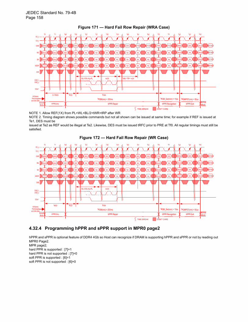
JEDEC Standard No. 79-4BPage 158
Figure 171 — Hard Fail Row Repair (WRA Case)
ACT
T1 Ta0 Td0 Td1 Te0 Te1Tb0 Tf1
WRA DES REF/DES
T0
MRS0
CK_c
CK_t
CMD
BG
DQS_t
CKE
TIME BREAK DON’T CARE
Tc0 Tc1
REF/DESMRS4 DES DES DES DES REF/DES PRE
Te2 Tf0
BGf BGf NA NAVALID NAVALID NA NA NA NA NA VALID
DQs1
Th0Tg0 Tg1
MRS4 REF/DESDES VALID
VALID REF/DESNA VALID
BAf BAf NA NAVALID NAVALID NA NA NA NA NA VALID VALID REF/DESNA VALID
ADDR
BA
VALID VALID NA NAVALID NAVALID
NA NA NA NA NA VALIDVALID
REF/DESNA VALID(A13=1) (A13=0)
DQS_c
hPPR Repair hPPR RecognitionNormal
All BanksPrecharged
and idle state
ModehPPR Entry hPPR Exit
NormalMode
5 X tMOD tRCD tPGM
tPGM(min) = 200ms
WL=CWL+AL+PL 4nCK tWR + tRP+ 1nCK
tPGM_Exit(min) = 15ns tPGMPST(min) = 50us
NOTE 1. Allow REF(1X) from PL+WL+BL/2+tWR+tRP after WRNOTE 2. Timing diagram shows possible commands but not all shown can be issued at same time; for example if REF is issued at Te1, DES must beissued at Te2 as REF would be illegal at Te2. Likewise, DES must be issued tRFC prior to PRE at Tf0. All regular timings must still be satisfied.
Figure 172 —
ACT
T1 Ta0 Td0 Td1 Te0 Te1Tb0 Tf1
WR DES DES
T0
MRS0
CK_c
CK_t
CMD
BG
DQS_t
CKE
TIME BREAK DON’T CARE
Tc0 Tc1
DESMRS4 DES DES DES DES DES PRE
Te2 Tf0
BGf BGf NA NAVALID NAVALID NA NA NA NA NA VALID
DQs1
Th0Tg0 Tg1
MRS4 REF/DESDES VALID
VALID REF/DESNA VALID
BAf BAf NA NAVALID NAVALID NA NA NA NA NA VALID VALID REF/DESNA VALID
ADDR
BA
VALID VALID NA NAVALID NAVALID
NA NA NA NA NA VALIDVALID
REF/DESNA VALID(A13=1) (A13=0)
DQS_c
hPPR Repair hPPR RecognitionNormal
All BanksPrecharged
and idle state
ModehPPR Entry hPPR Exit
NormalMode
tMOD tRCD tPGM
tPGM(min) = 200ms
WL=CWL+AL+PL 4nCK
tPGM_Exit(min) = 15ns tPGMPST(min) = 50us
Hard Fail Row Repair (WR Case)
4.32.4 Programming hPPR and sPPR support in MPR0 page2
hPPR and sPPR is optional feature of DDR4 4Gb so Host can recognize if DRAM is supporting hPPR and sPPR or not by reading out MPR0 Page2.MPR page2;hard PPR is supported : [7]=1hard PPR is not supported : [7]=0soft PPR is supported : [6]=1soft PPR is not supported : [6]=0
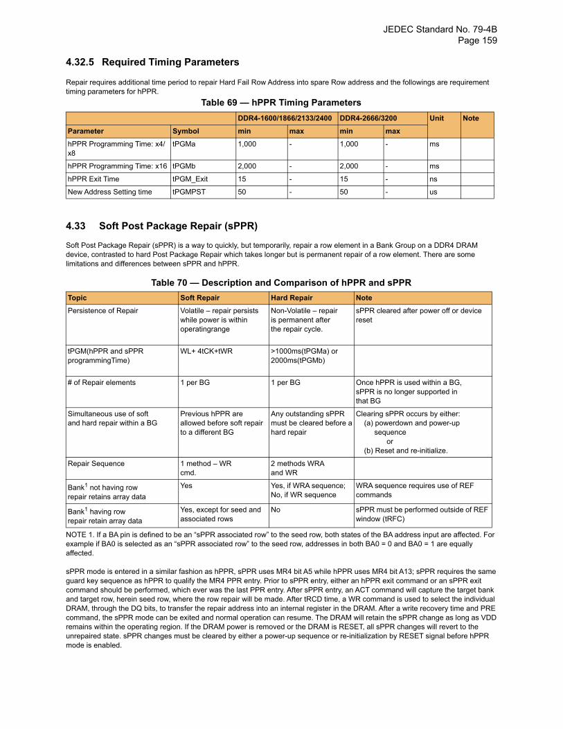
JEDEC Standard No. 79-4B Page 159
4.32.5 Required Timing Parameters
Repair requires additional time period to repair Hard Fail Row Address into spare Row address and the followings are requirement timing parameters for hPPR.
Table 69 — hPPR Timing Parameters
4.33 Soft Post Package Repair (sPPR)
Soft Post Package Repair (sPPR) is a way to quickly, but temporarily, repair a row element in a Bank Group on a DDR4 DRAM device, contrasted to hard Post Package Repair which takes longer but is permanent repair of a row element. There are some limitations and differences between sPPR and hPPR.
Table 70 — Description and Comparison of hPPR and sPPR
NOTE 1. If a BA pin is defined to be an “sPPR associated row” to the seed row, both states of the BA address input are affected. For example if BA0 is selected as an “sPPR associated row” to the seed row, addresses in both BA0 = 0 and BA0 = 1 are equally affected.
sPPR mode is entered in a similar fashion as hPPR, sPPR uses MR4 bit A5 while hPPR uses MR4 bit A13; sPPR requires the sameguard key sequence as hPPR to qualify the MR4 PPR entry. Prior to sPPR entry, either an hPPR exit command or an sPPR exitcommand should be performed, which ever was the last PPR entry. After sPPR entry, an ACT command will capture the target bankand target row, herein seed row, where the row repair will be made. After tRCD time, a WR command is used to select the individualDRAM, through the DQ bits, to transfer the repair address into an internal register in the DRAM. After a write recovery time and PREcommand, the sPPR mode can be exited and normal operation can resume. The DRAM will retain the sPPR change as long as VDDremains within the operating region. If the DRAM power is removed or the DRAM is RESET, all sPPR changes will revert to the unrepaired state. sPPR changes must be cleared by either a power-up sequence or re-initialization by RESET signal before hPPRmode is enabled.
DDR4-1600/1866/2133/2400 DDR4-2666/3200 Unit Note
Parameter Symbol min max min max
hPPR Programming Time: x4/x8
tPGMa 1,000 - 1,000 - ms
hPPR Programming Time: x16 tPGMb 2,000 - 2,000 - ms
hPPR Exit Time tPGM_Exit 15 - 15 - ns
New Address Setting time tPGMPST 50 - 50 - us
Topic Soft Repair Hard Repair Note
Persistence of Repair Volatile – repair persistswhile power is within operatingrange
Non-Volatile – repairis permanent afterthe repair cycle.
sPPR cleared after power off or devicereset
tPGM(hPPR and sPPR programmingTime)
WL+ 4tCK+tWR >1000ms(tPGMa) or2000ms(tPGMb)
# of Repair elements 1 per BG 1 per BG Once hPPR is used within a BG,sPPR is no longer supported inthat BG
Simultaneous use of softand hard repair within a BG
Previous hPPR are allowed before soft repair to a different BG
Any outstanding sPPR must be cleared before ahard repair
Clearing sPPR occurs by either: (a) powerdown and power-up sequence or (b) Reset and re-initialize.
Repair Sequence 1 method – WRcmd.
2 methods WRAand WR
Bank1 not having rowrepair retains array data
Yes Yes, if WRA sequence; No, if WR sequence
WRA sequence requires use of REF commands
Bank1 having rowrepair retain array data
Yes, except for seed and associated rows
No sPPR must be performed outside of REF window (tRFC)
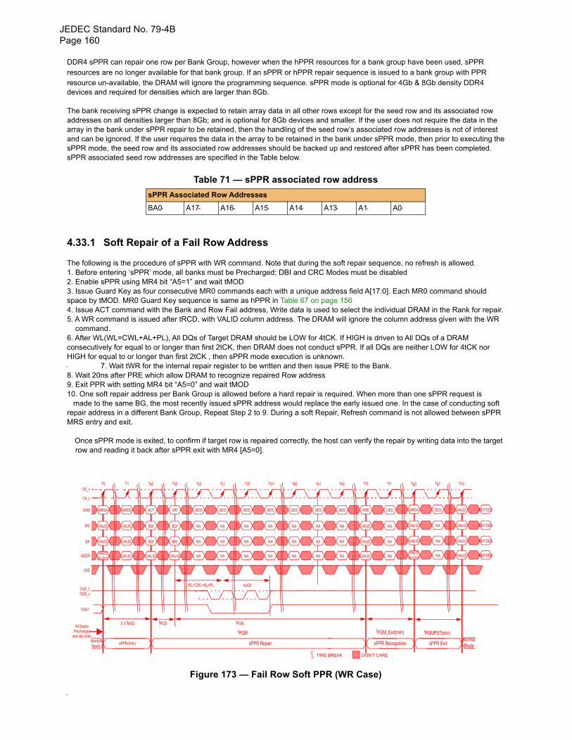
JEDEC Standard No. 79-4BPage 160
DDR4 sPPR can repair one row per Bank Group, however when the hPPR resources for a bank group have been used, sPPRresources are no longer available for that bank group. If an sPPR or hPPR repair sequence is issued to a bank group with PPR resource un-available, the DRAM will ignore the programming sequence. sPPR mode is optional for 4Gb & 8Gb density DDR4 devices and required for densities which are larger than 8Gb.
The bank receiving sPPR change is expected to retain array data in all other rows except for the seed row and its associated rowaddresses on all densities larger than 8Gb; and is optional for 8Gb devices and smaller. If the user does not require the data in thearray in the bank under sPPR repair to be retained, then the handling of the seed row’s associated row addresses is not of interestand can be ignored. If the user requires the data in the array to be retained in the bank under sPPR mode, then prior to executing thesPPR mode, the seed row and its associated row addresses should be backed up and restored after sPPR has been completed.sPPR associated seed row addresses are specified in the Table below.
Table 71 — sPPR associated row address
4.33.1 Soft Repair of a Fail Row Address
The following is the procedure of sPPR with WR command. Note that during the soft repair sequence, no refresh is allowed.1. Before entering ‘sPPR’ mode, all banks must be Precharged; DBI and CRC Modes must be disabled2. Enable sPPR using MR4 bit “A5=1” and wait tMOD3. Issue Guard Key as four consecutive MR0 commands each with a unique address field A[17:0]. Each MR0 command should space by tMOD. MR0 Guard Key sequence is same as hPPR in Table 67 on page 1564. Issue ACT command with the Bank and Row Fail address, Write data is used to select the individual DRAM in the Rank for repair.5. A WR command is issued after tRCD, with VALID column address. The DRAM will ignore the column address given with the WR command.6. After WL(WL=CWL+AL+PL), All DQs of Target DRAM should be LOW for 4tCK. If HIGH is driven to All DQs of a DRAM consecutively for equal to or longer than first 2tCK, then DRAM does not conduct sPPR. If all DQs are neither LOW for 4tCK nor HIGH for equal to or longer than first 2tCK , then sPPR mode execution is unknown.
7. Wait tWR for the internal repair register to be written and then issue PRE to the Bank.8. Wait 20ns after PRE which allow DRAM to recognize repaired Row address9. Exit PPR with setting MR4 bit “A5=0” and wait tMOD10. One soft repair address per Bank Group is allowed before a hard repair is required. When more than one sPPR request is made to the same BG, the most recently issued sPPR address would replace the early issued one. In the case of conducting soft repair address in a different Bank Group, Repeat Step 2 to 9. During a soft Repair, Refresh command is not allowed between sPPR MRS entry and exit. Once sPPR mode is exited, to confirm if target row is repaired correctly, the host can verify the repair by writing data into the target row and reading it back after sPPR exit with MR4 [A5=0].
Figure 173 — Fail Row Soft PPR (WR Case)
sPPR Associated Row Addresses
BA0 A17 A16 A15 A14 A13 A1 A0
ACT
T1 Ta0 Td0 Td1 Te0 Te1Tb0 Tf1
WR DES DES
T0
MRS0
CK_c
CK_t
CMD
BG
DQS_t
CKE
TIME BREAK DON’T CARE
Tc0 Tc1
DESMRS4 DES DES DES DES DES PRE
Te2 Tf0
BGf BGf NA NAVALID NAVALID NA NA NA NA NA VALID
DQs1
Th0Tg0 Tg1
MRS4 REF/DESDES VALID
VALID REF/DESNA VALID
BAf BAf NA NAVALID NAVALID NA NA NA NA NA VALID VALID REF/DESNA VALID
ADDR
BA
VALID VALID NA NAVALID NAVALID
NA NA NA NA NA VALIDVALID
REF/DESNA VALID(A13=1) (A13=0)
DQS_c
sPPR Repair sPPR RecognitionNormal
All BanksPrecharged
and idle state
ModesPPR Entry sPPR Exit
NormalMode
5 X tMOD tRCD tPGM
tPGM
WL=CWL+AL+PL 4nCK
tPGM_Exit(min) tPGMPST(min)
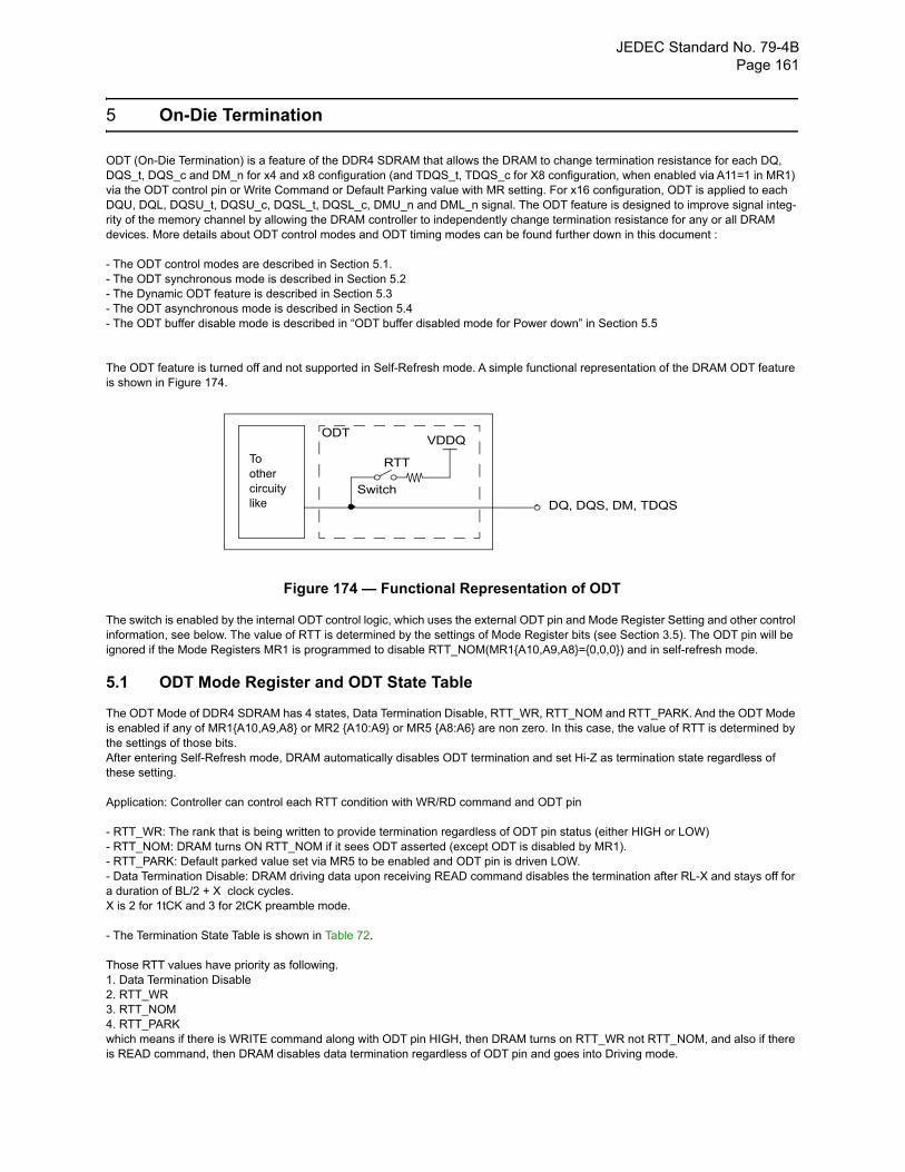
JEDEC Standard No. 79-4B Page 161
5 On-Die Termination
ODT (On-Die Termination) is a feature of the DDR4 SDRAM that allows the DRAM to change termination resistance for each DQ, DQS_t, DQS_c and DM_n for x4 and x8 configuration (and TDQS_t, TDQS_c for X8 configuration, when enabled via A11=1 in MR1) via the ODT control pin or Write Command or Default Parking value with MR setting. For x16 configuration, ODT is applied to each DQU, DQL, DQSU_t, DQSU_c, DQSL_t, DQSL_c, DMU_n and DML_n signal. The ODT feature is designed to improve signal integ-rity of the memory channel by allowing the DRAM controller to independently change termination resistance for any or all DRAM devices. More details about ODT control modes and ODT timing modes can be found further down in this document :
- The ODT control modes are described in Section 5.1. - The ODT synchronous mode is described in Section 5.2 - The Dynamic ODT feature is described in Section 5.3 - The ODT asynchronous mode is described in Section 5.4 - The ODT buffer disable mode is described in “ODT buffer disabled mode for Power down” in Section 5.5
The ODT feature is turned off and not supported in Self-Refresh mode. A simple functional representation of the DRAM ODT feature is shown in Figure 174.
Figure 174 — Functional Representation of ODT
The switch is enabled by the internal ODT control logic, which uses the external ODT pin and Mode Register Setting and other control information, see below. The value of RTT is determined by the settings of Mode Register bits (see Section 3.5). The ODT pin will be ignored if the Mode Registers MR1 is programmed to disable RTT_NOM(MR1{A10,A9,A8}={0,0,0}) and in self-refresh mode.
5.1 ODT Mode Register and ODT State Table
The ODT Mode of DDR4 SDRAM has 4 states, Data Termination Disable, RTT_WR, RTT_NOM and RTT_PARK. And the ODT Mode is enabled if any of MR1{A10,A9,A8} or MR2 {A10:A9} or MR5 {A8:A6} are non zero. In this case, the value of RTT is determined by the settings of those bits. After entering Self-Refresh mode, DRAM automatically disables ODT termination and set Hi-Z as termination state regardless of these setting.
Application: Controller can control each RTT condition with WR/RD command and ODT pin
- RTT_WR: The rank that is being written to provide termination regardless of ODT pin status (either HIGH or LOW) - RTT_NOM: DRAM turns ON RTT_NOM if it sees ODT asserted (except ODT is disabled by MR1). - RTT_PARK: Default parked value set via MR5 to be enabled and ODT pin is driven LOW. - Data Termination Disable: DRAM driving data upon receiving READ command disables the termination after RL-X and stays off for a duration of BL/2 + X clock cycles. X is 2 for 1tCK and 3 for 2tCK preamble mode.
- The Termination State Table is shown in Table 72.
Those RTT values have priority as following. 1. Data Termination Disable 2. RTT_WR 3. RTT_NOM 4. RTT_PARK which means if there is WRITE command along with ODT pin HIGH, then DRAM turns on RTT_WR not RTT_NOM, and also if there is READ command, then DRAM disables data termination regardless of ODT pin and goes into Driving mode.
RTTToothercircuitylike
ODTVDDQ
SwitchDQ, DQS, DM, TDQS
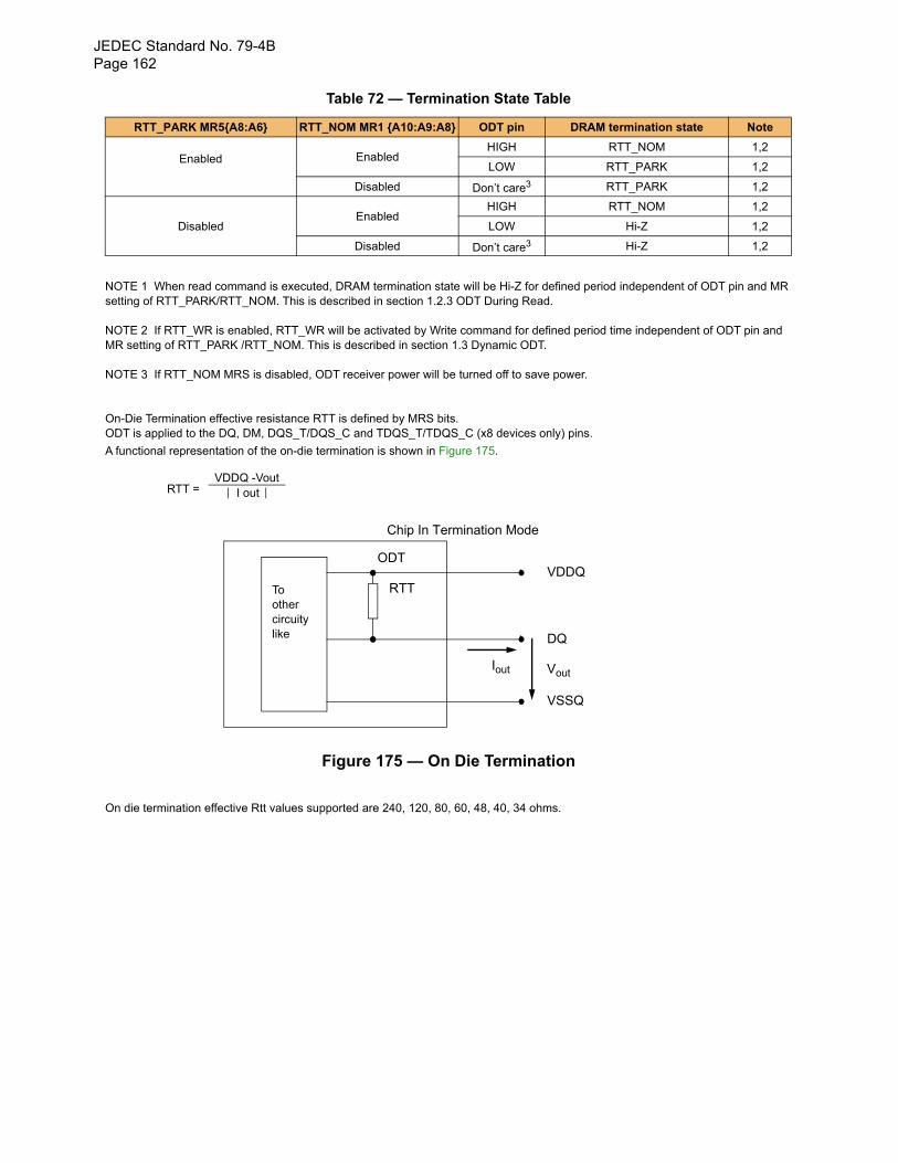
JEDEC Standard No. 79-4BPage 162
Table 72 — Termination State Table
NOTE 1 When read command is executed, DRAM termination state will be Hi-Z for defined period independent of ODT pin and MR setting of RTT_PARK/RTT_NOM. This is described in section 1.2.3 ODT During Read.
NOTE 2 If RTT_WR is enabled, RTT_WR will be activated by Write command for defined period time independent of ODT pin and MR setting of RTT_PARK /RTT_NOM. This is described in section 1.3 Dynamic ODT.
NOTE 3 If RTT_NOM MRS is disabled, ODT receiver power will be turned off to save power.
On-Die Termination effective resistance RTT is defined by MRS bits. ODT is applied to the DQ, DM, DQS_T/DQS_C and TDQS_T/TDQS_C (x8 devices only) pins.
A functional representation of the on-die termination is shown in Figure 175.
Figure 175 — On Die Termination
On die termination effective Rtt values supported are 240, 120, 80, 60, 48, 40, 34 ohms.
RTT_PARK MR5{A8:A6} RTT_NOM MR1 {A10:A9:A8} ODT pin DRAM termination state Note
Enabled EnabledHIGH RTT_NOM 1,2
LOW RTT_PARK 1,2
Disabled Don’t care3 RTT_PARK 1,2
DisabledEnabled
HIGH RTT_NOM 1,2
LOW Hi-Z 1,2
Disabled Don’t care3 Hi-Z 1,2
RTT = VDDQ -Vout
I out
Toothercircuitylike
ODT
DQ
RTT
VSSQ
VDDQ
Iout Vout
Chip In Termination Mode
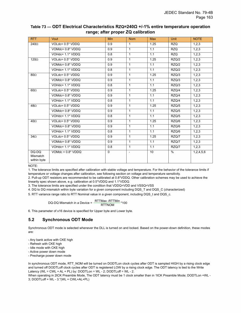
JEDEC Standard No. 79-4B Page 163
Table 73 — ODT Electrical Characteristics RZQ=240Ω +/-1% entire temperature operation range; after proper ZQ calibration
NOTE: 1. The tolerance limits are specified after calibration with stable voltage and temperature. For the behavior of the tolerance limits if temperature or voltage changes after calibration, see following section on voltage and temperature sensitivity. 2. Pull-up ODT resistors are recommended to be calibrated at 0.8*VDDQ. Other calibration schemes may be used to achieve the linearity spec shown above, e.g. calibration at 0.5*VDDQ and 1.1*VDDQ. 3. The tolerance limits are specified under the condition that VDDQ=VDD and VSSQ=VSS 4. DQ to DQ mismatch within byte variation for a given component including DQS_T and DQS_C (characterized)
5. RTT variance range ratio to RTT Nominal value in a given component, including DQS_t and DQS_c.
6. This parameter of x16 device is specified for Upper byte and Lower byte.
5.2 Synchronous ODT Mode
Synchronous ODT mode is selected whenever the DLL is turned on and locked. Based on the power-down definition, these modes are:
- Any bank active with CKE high - Refresh with CKE high - Idle mode with CKE high - Active power down mode - Precharge power down mode
In synchronous ODT mode, RTT_NOM will be turned on DODTLon clock cycles after ODT is sampled HIGH by a rising clock edge and turned off DODTLoff clock cycles after ODT is registered LOW by a rising clock edge. The ODT latency is tied to the Write Latency (WL = CWL + AL + PL) by: DODTLon = WL - 2; DODTLoff = WL - 2. When operating in 2tCK Preamble Mode, The ODT latency must be 1 clock smaller than in 1tCK Preamble Mode; DODTLon =WL - 3; DODTLoff = WL - 3."(WL = CWL+AL+PL)
RTT Vout Min Nom Max Unit NOTE
240 VOLdc= 0.5* VDDQ 0.9 1 1.25 RZQ 1,2,3
VOMdc= 0.8* VDDQ 0.9 1 1.1 RZQ 1,2,3
VOHdc= 1.1* VDDQ 0.8 1 1.1 RZQ 1,2,3
120 VOLdc= 0.5* VDDQ 0.9 1 1.25 RZQ/2 1,2,3
VOMdc= 0.8* VDDQ 0.9 1 1.1 RZQ/2 1,2,3
VOHdc= 1.1* VDDQ 0.8 1 1.1 RZQ/2 1,2,3
80 VOLdc= 0.5* VDDQ 0.9 1 1.25 RZQ/3 1,2,3
VOMdc= 0.8* VDDQ 0.9 1 1.1 RZQ/3 1,2,3
VOHdc= 1.1* VDDQ 0.8 1 1.1 RZQ/3 1,2,3
60 VOLdc= 0.5* VDDQ 0.9 1 1.25 RZQ/4 1,2,3
VOMdc= 0.8* VDDQ 0.9 1 1.1 RZQ/4 1,2,3
VOHdc= 1.1* VDDQ 0.8 1 1.1 RZQ/4 1,2,3
48 VOLdc= 0.5* VDDQ 0.9 1 1.25 RZQ/5 1,2,3
VOMdc= 0.8* VDDQ 0.9 1 1.1 RZQ/5 1,2,3
VOHdc= 1.1* VDDQ 0.8 1 1.1 RZQ/5 1,2,3
40 VOLdc= 0.5* VDDQ 0.9 1 1.25 RZQ/6 1,2,3
VOMdc= 0.8* VDDQ 0.9 1 1.1 RZQ/6 1,2,3
VOHdc= 1.1* VDDQ 0.8 1 1.1 RZQ/6 1,2,3
34 VOLdc= 0.5* VDDQ 0.9 1 1.25 RZQ/7 1,2,3
VOMdc= 0.8* VDDQ 0.9 1 1.1 RZQ/7 1,2,3
VOHdc= 1.1* VDDQ 0.8 1 1.1 RZQ/7 1,2,3
DQ-DQ Mismatch within byte
VOMdc = 0.8* VDDQ 0 - 10 % 1,2,4,5,6
*100RTTMax -RTTMin
RTTNOMDQ-DQ Mismatch in a Device =
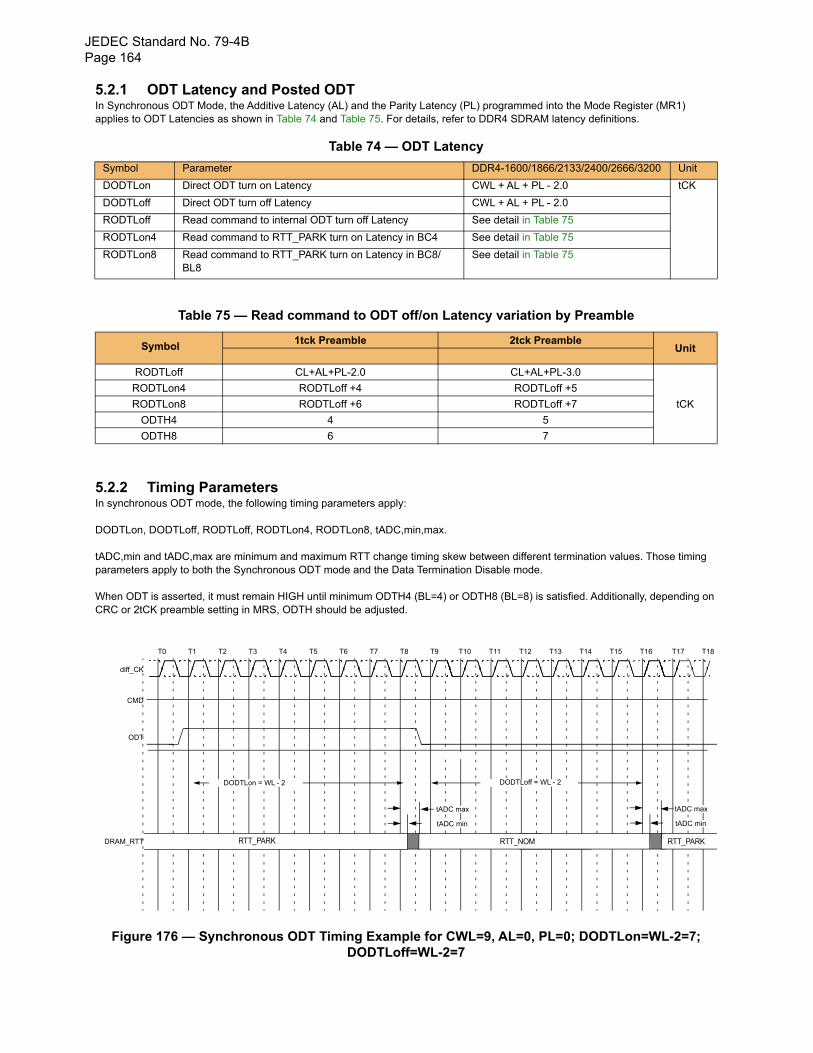
JEDEC Standard No. 79-4BPage 164
5.2.1 ODT Latency and Posted ODTIn Synchronous ODT Mode, the Additive Latency (AL) and the Parity Latency (PL) programmed into the Mode Register (MR1) applies to ODT Latencies as shown in Table 74 and Table 75. For details, refer to DDR4 SDRAM latency definitions.
Table 74 — ODT Latency
Table 75 — Read command to ODT off/on Latency variation by Preamble
5.2.2 Timing ParametersIn synchronous ODT mode, the following timing parameters apply:
DODTLon, DODTLoff, RODTLoff, RODTLon4, RODTLon8, tADC,min,max.
tADC,min and tADC,max are minimum and maximum RTT change timing skew between different termination values. Those timing parameters apply to both the Synchronous ODT mode and the Data Termination Disable mode.
When ODT is asserted, it must remain HIGH until minimum ODTH4 (BL=4) or ODTH8 (BL=8) is satisfied. Additionally, depending on CRC or 2tCK preamble setting in MRS, ODTH should be adjusted.
Figure 176 — Synchronous ODT Timing Example for CWL=9, AL=0, PL=0; DODTLon=WL-2=7; DODTLoff=WL-2=7
Symbol Parameter DDR4-1600/1866/2133/2400/2666/3200 Unit
DODTLon Direct ODT turn on Latency CWL + AL + PL - 2.0 tCK
DODTLoff Direct ODT turn off Latency CWL + AL + PL - 2.0
RODTLoff Read command to internal ODT turn off Latency See detail in Table 75
RODTLon4 Read command to RTT_PARK turn on Latency in BC4 See detail in Table 75
RODTLon8 Read command to RTT_PARK turn on Latency in BC8/BL8
See detail in Table 75
Symbol1tck Preamble 2tck Preamble
Unit
RODTLoff CL+AL+PL-2.0 CL+AL+PL-3.0
tCK
RODTLon4 RODTLoff +4 RODTLoff +5
RODTLon8 RODTLoff +6 RODTLoff +7
ODTH4 4 5
ODTH8 6 7
T0 T1 T2 T3 T4 T5 T6 T7 T8 T9 T10 T11 T12 T13 T14 T15 T16
diff_CK
ODT
DRAM_RTT
T17 T18
CMD
tADC min
tADC max
DODTLon = WL - 2 DODTLoff = WL - 2
RTT_NOM
tADC min
tADC max
RTT_PARK RTT_NOM RTT_PARK
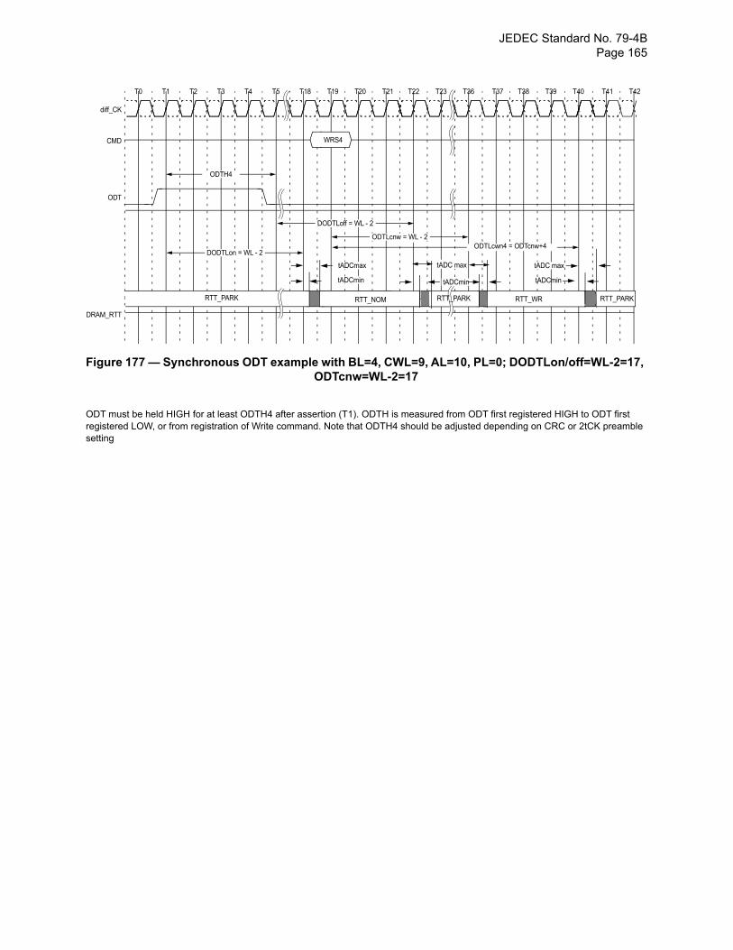
JEDEC Standard No. 79-4B Page 165
Figure 177 — Synchronous ODT example with BL=4, CWL=9, AL=10, PL=0; DODTLon/off=WL-2=17, ODTcnw=WL-2=17
ODT must be held HIGH for at least ODTH4 after assertion (T1). ODTH is measured from ODT first registered HIGH to ODT first registered LOW, or from registration of Write command. Note that ODTH4 should be adjusted depending on CRC or 2tCK preamble setting
T0 T1 T2 T3 T4 T5 T18 T19 T20 T21 T22 T23 T36 T37 T38 T39 T40
diff_CK
ODT
DRAM_RTT
T41 T42
CMD
tADCmin
tADCmax
ODTH4
RTT_NOM
tADC max
WRS4
DODTLoff = WL - 2
ODTLcwn4 = ODTcnw+4ODTLcnw = WL - 2
DODTLon = WL - 2
tADCmin
RTT_WR
tADC max
tADCmin
RTT_PARK RTT_PARK RTT_PARK
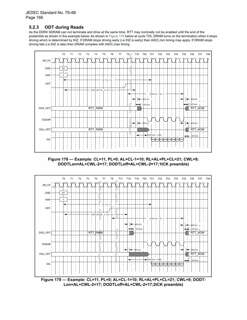
JEDEC Standard No. 79-4BPage 166
5.2.3 ODT during ReadsAs the DDR4 SDRAM can not terminate and drive at the same time. RTT may nominally not be enabled until the end of the postamble as shown in the example below. As shown in Figure 178 below at cycle T25, DRAM turns on the termination when it stops driving which is determined by tHZ. If DRAM stops driving early (i.e tHZ is early) then tADC,min timing may apply. If DRAM stops driving late (i.e tHZ is late) then DRAM complies with tADC,max timing.
Figure 178 — Example: CL=11, PL=0; AL=CL-1=10; RL=AL+PL+CL=21; CWL=9; DODTLon=AL+CWL-2=17; DODTLoff=AL+CWL-2=17;1tCK preamble)
Figure 179 — Example: CL=11, PL=0; AL=CL-1=10; RL=AL+PL+CL=21; CWL=9; DODT-Lon=AL+CWL-2=17; DODTLoff=AL+CWL-2=17;2tCK preamble)
diff_CK
CMD
RL = AL + CL
tADCmax
ODT
DQS_ODT
RD
T0 T1 T2 T3 T4 T5 T6 T7 T8 T19 T21 T22 T23 T24 T25 T26 T27 T28T20
Addr A
RODTLoff = RL - 2 = CL + AL - 2
DODTLon = WL - 2
tADCmin
RTT_PARK
tADCmin
RTT_NOM
DQSdiff
QA0 QA1 QA2 QA3 QA4 QA5 QA6 QA7DQ
tADCmax
tADCmax + 1nCK
DQs_ODT RTT_PARK RTT_NOM
tADCmax
tADCmin tADCmin
diff_CK
CMD
RL = AL + CL
ODT
DQS_ODT
RD
T0 T1 T2 T3 T4 T7 T8 T17 T18 T19 T21 T22 T23 T24 T25 T26 T27 T28T20
Addr A
RODTLoff = RL - 2 = CL + AL - 3
DODTLon = WL - 2
tADCmin tADCmin
RTT_NOM
DQSdiff
QA0 QA1 QA2 QA3 QA4 QA5 QA6 QA7DQ
tADCmax
tADCmax + 2nCK
DQs_ODT RTT_PARK RTT_NOM
tADCmax
tADCmin tADCmin
tADCmax
RTT_PARK
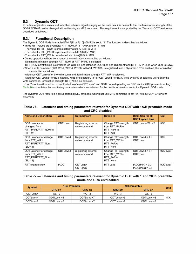
JEDEC Standard No. 79-4B Page 167
5.3 Dynamic ODTIn certain application cases and to further enhance signal integrity on the data bus, it is desirable that the termination strength of the DDR4 SDRAM can be changed without issuing an MRS command. This requirement is supported by the “Dynamic ODT” feature as described as follows:
5.3.1 Functional DescriptionThe Dynamic ODT Mode is enabled if bit A[9] or A[10] of MR2 is set to ’1’. The function is described as follows:• Three RTT values are available: RTT_NOM, RTT_PARK and RTT_WR. - The value for RTT_NOM is preselected via bits A[10:8] in MR1 - The value for RTT_PARK is preselected via bits A[8:6] in MR5 - The value for RTT_WR is preselected via bits A[10:9] in MR2 • During operation without commands, the termination is controlled as follows; - Nominal termination strength RTT_NOM or RTT_PARK is selected. - RTT_NOM on/off timing is controlled via ODT pin and latencies DODTLon and DODTLoff and RTT_PARK is on when ODT is LOW.• When a write command (WR, WRA, WRS4, WRS8, WRAS4, WRAS8) is registered, and if Dynamic ODT is enabled, the termination
is controlled as follows: - A latency ODTLcnw after the write command, termination strength RTT_WR is selected. - A latency ODTLcwn8 (for BL8, fixed by MRS or selected OTF) or ODTLcwn4 (for BC4, fixed by MRS or selected OTF) after the write command, termination strength RTT_WR is de-selected. - 1 or 2 clocks will be added or subtracted into/from ODTLcwn8 and ODTLcwn4 depending on CRC and/or 2tCK preamble setting.Table 76 shows latencies and timing parameters which are relevant for the on-die termination control in Dynamic ODT mode.
The Dynamic ODT feature is not supported at DLL-off mode. User must use MRS command to set Rtt_WR, MR2{A10,A9}={0,0} externally.
Table 76 — Latencies and timing parameters relevant for Dynamic ODT with 1tCK preamble mode and CRC disabled
Table 77 — Latencies and timing parameters relevant for Dynamic ODT with 1 and 2tCK preamble mode and CRC en/disabled
Name and Description Abbr. Defined from Define to Definition for all DDR4 speed bins
Unit
ODT Latency for changing from RTT_PARK/RTT_NOM to RTT_WR
ODTLcnw Registering external write command
Change RTT strength from RTT_PARK/RTT_Nom to RTT_WR
ODTLcnw = WL - 2 tCK
ODT Latency for change from RTT_WR to RTT_PARK/RTT_Nom (BL = 4)
ODTLcwn4 Registering external write command
Change RTT strength from RTT_WR to RTT_PARK/RTT_Nom
ODTLcwn4 = 4 + ODTLcnw
tCK
ODT Latency for change from RTT_WR to RTT_PARK/RTT_Nom (BL = 8)
ODTLcwn8 registering external write command
Change RTT strength from RTT_WR to RTT_PARK/RTT_Nom
ODTLcwn8 = 6 + ODTLcnw
tCK(avg)
RTT change skew tADC ODTLcnwODTLcwn
RTT valid tADC(min) = 0.3tADC(max) = 0.7
tCK(avg)
Symbol1tck Preamble 2tck Preamble
UnitCRC off CRC on CRC off CRC on
ODTLcnw WL - 2 WL - 2 WL - 3 WL - 3
tCKODTLcwn4 ODTLcnw +4 ODTLcnw +7 ODTLcnw +5 ODTLcnw +8
ODTLcwn8 ODTLcnw +6 ODTLcnw +7 ODTLcnw +7 ODTLcnw +8
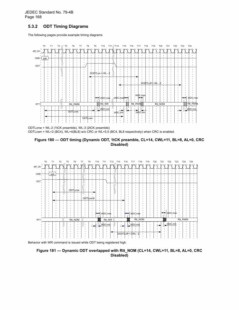
JEDEC Standard No. 79-4BPage 168
5.3.2 ODT Timing Diagrams
The following pages provide example timing diagrams
ODTLcnw = WL-2 (1tCK preamble), WL-3 (2tCK preamble)ODTLcwn = WL+2 (BC4), WL+4(BL8) w/o CRC or WL+5,5 (BC4, BL8 respectively) when CRC is enabled.
Figure 180 — ODT timing (Dynamic ODT, 1tCK preamble, CL=14, CWL=11, BL=8, AL=0, CRC Disabled)
Behavior with WR command is issued while ODT being registered high.
Figure 181 — Dynamic ODT overlapped with Rtt_NOM (CL=14, CWL=11, BL=8, AL=0, CRC Disabled)
diff_CK
CMD
ODT
RTT
DODTLon = WL - 2
DODTLoff = WL - 2
tADC,max
tADC,min
tADC,max
tADC,min
Rtt_WRRtt_PARK
WR
ODTLcnw
ODTLcwn
Rtt_NOM
tADC,min
tADC,max
Rtt_PARK
tADC,max
tADC,min
Rtt_PARK
T0 T1 T2 T5 T6 T7 T8 T9 T10 T11 T14 T15 T16 T17 T18 T19 T20 T21 T22 T23 T24
diff_CK
ODT
RTT
ODTLcnw
ODTLcwn8
tADC,max
tADC,min
tADC,max
tADC,min
WR
DODTLoff = CWL - 2
Rtt_NOM
CMD
Rtt_NOM Rtt_WR
tADC,max
tADC,min
Rtt_PARK
T0 T1 T2 T5 T6 T7 T9 T10 T11 T12 T15 T16 T17 T18 T19 T20 T21 T22 T23 T24 T25
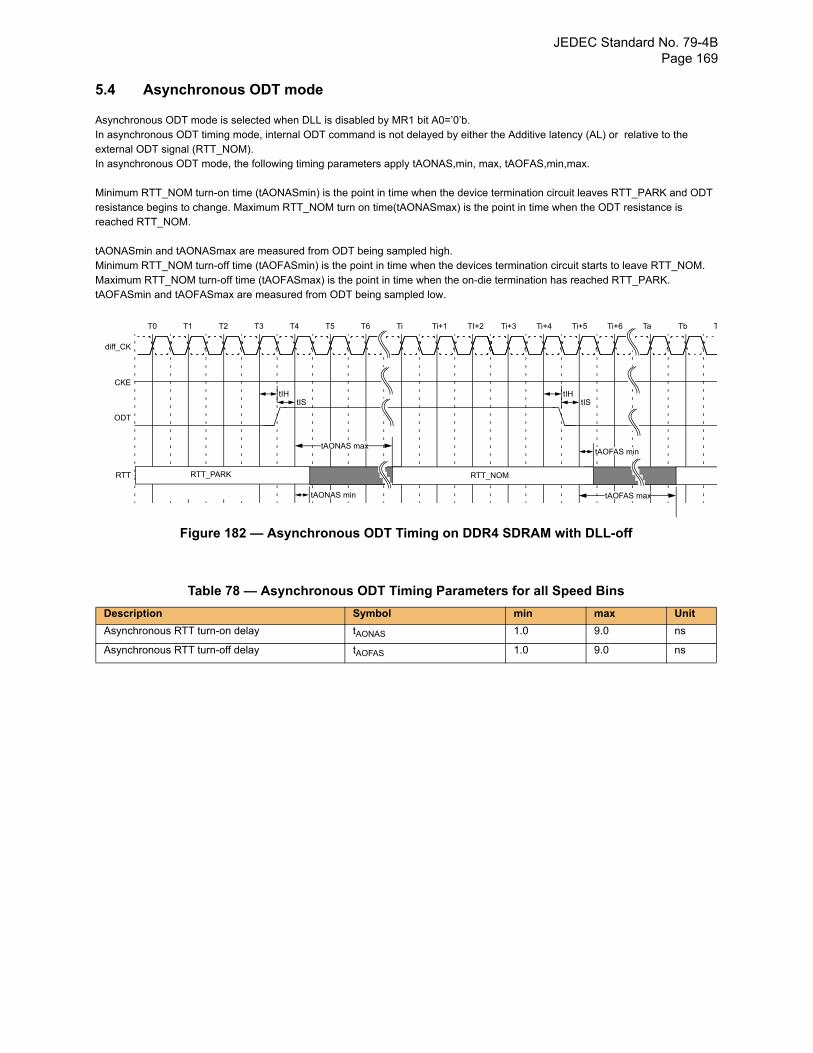
JEDEC Standard No. 79-4B Page 169
5.4 Asynchronous ODT mode
Asynchronous ODT mode is selected when DLL is disabled by MR1 bit A0=’0’b. In asynchronous ODT timing mode, internal ODT command is not delayed by either the Additive latency (AL) or relative to the external ODT signal (RTT_NOM).In asynchronous ODT mode, the following timing parameters apply tAONAS,min, max, tAOFAS,min,max.
Minimum RTT_NOM turn-on time (tAONASmin) is the point in time when the device termination circuit leaves RTT_PARK and ODT resistance begins to change. Maximum RTT_NOM turn on time(tAONASmax) is the point in time when the ODT resistance is reached RTT_NOM.
tAONASmin and tAONASmax are measured from ODT being sampled high. Minimum RTT_NOM turn-off time (tAOFASmin) is the point in time when the devices termination circuit starts to leave RTT_NOM. Maximum RTT_NOM turn-off time (tAOFASmax) is the point in time when the on-die termination has reached RTT_PARK. tAOFASmin and tAOFASmax are measured from ODT being sampled low.
Figure 182 — Asynchronous ODT Timing on DDR4 SDRAM with DLL-off
Table 78 — Asynchronous ODT Timing Parameters for all Speed Bins
Description Symbol min max Unit
Asynchronous RTT turn-on delay tAONAS 1.0 9.0 ns
Asynchronous RTT turn-off delay tAOFAS 1.0 9.0 ns
T0 T1 T2 T3 T4 T5 T6 Ti Ti+1 TI+2 Ti+3 Ti+4 Ti+5 Ti+6 Ta Tb T
diff_CK
CKE
ODT
RTT
tIHtIS
RTT_NOM
tAONAS max
tAONAS min
tIHtIS
tAOFAS min
tAOFAS max
TD_ODT_AsyncRTT_PARK
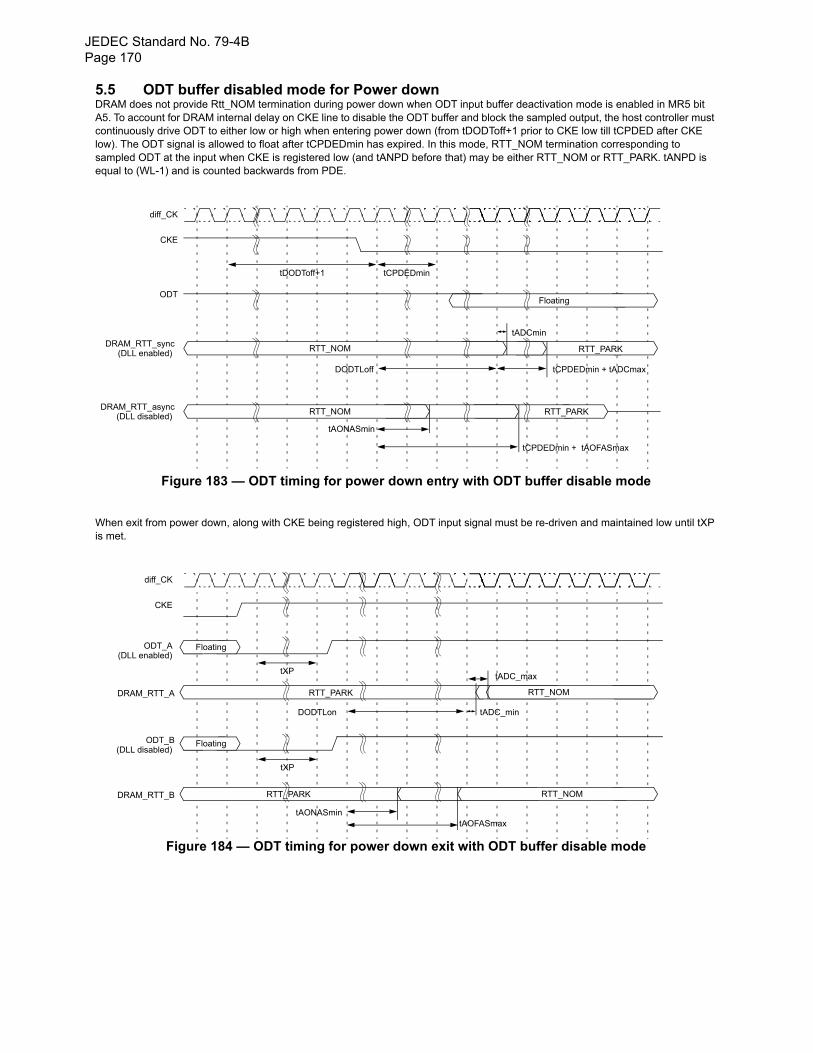
JEDEC Standard No. 79-4BPage 170
5.5 ODT buffer disabled mode for Power downDRAM does not provide Rtt_NOM termination during power down when ODT input buffer deactivation mode is enabled in MR5 bit A5. To account for DRAM internal delay on CKE line to disable the ODT buffer and block the sampled output, the host controller must continuously drive ODT to either low or high when entering power down (from tDODToff+1 prior to CKE low till tCPDED after CKE low). The ODT signal is allowed to float after tCPDEDmin has expired. In this mode, RTT_NOM termination corresponding to sampled ODT at the input when CKE is registered low (and tANPD before that) may be either RTT_NOM or RTT_PARK. tANPD is equal to (WL-1) and is counted backwards from PDE.
Figure 183 — ODT timing for power down entry with ODT buffer disable mode
When exit from power down, along with CKE being registered high, ODT input signal must be re-driven and maintained low until tXP is met.
Figure 184 — ODT timing for power down exit with ODT buffer disable mode
tDODToff+1 tCPDEDmin
diff_CK
CKE
ODT
DRAM_RTT_sync
DRAM_RTT_async
Floating
RTT_NOM
RTT_NOM
DODTLoff
tADCmin
tCPDEDmin + tADCmax
tAONASmin
tCPDEDmin + tAOFASmax
(DLL enabled)
(DLL disabled)
RTT_PARK
RTT_PARK
diff_CK
CKE
ODT_A
DRAM_RTT_A
ODT_B(DLL disabled)
Floating
tADC_minDODTLon
tXP
Floating
tXP
tAONASmin
(DLL enabled)
DRAM_RTT_B
RTT_NOM
tADC_max
RTT_PARK
RTT_NOM
tAOFASmax
RTT_PARK
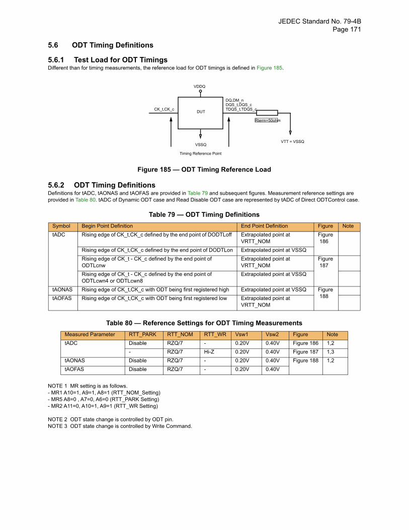
JEDEC Standard No. 79-4B Page 171
5.6 ODT Timing Definitions
5.6.1 Test Load for ODT Timings Different than for timing measurements, the reference load for ODT timings is defined in Figure 185.
Figure 185 — ODT Timing Reference Load
5.6.2 ODT Timing Definitions Definitions for tADC, tAONAS and tAOFAS are provided in Table 79 and subsequent figures. Measurement reference settings areprovided in Table 80. tADC of Dynamic ODT case and Read Disable ODT case are represented by tADC of Direct ODTControl case.
Table 79 — ODT Timing Definitions
Table 80 — Reference Settings for ODT Timing Measurements
NOTE 1 MR setting is as follows. - MR1 A10=1, A9=1, A8=1 (RTT_NOM_Setting) - MR5 A8=0 , A7=0, A6=0 (RTT_PARK Setting)- MR2 A11=0, A10=1, A9=1 (RTT_WR Setting)
NOTE 2 ODT state change is controlled by ODT pin.NOTE 3 ODT state change is controlled by Write Command.
Symbol Begin Point Definition End Point Definition Figure Note
tADC Rising edge of CK_t,CK_c defined by the end point of DODTLoff Extrapolated point at VRTT_NOM
Figure 186
Rising edge of CK_t,CK_c defined by the end point of DODTLon Extrapolated point at VSSQ
Rising edge of CK_t - CK_c defined by the end point of ODTLcnw
Extrapolated point atVRTT_NOM
Figure 187
Rising edge of CK_t - CK_c defined by the end point ofODTLcwn4 or ODTLcwn8
Extrapolated point at VSSQ
tAONAS Rising edge of CK_t,CK_c with ODT being first registered high Extrapolated point at VSSQ Figure 188tAOFAS Rising edge of CK_t,CK_c with ODT being first registered low Extrapolated point at
VRTT_NOM
Measured Parameter RTT_PARK RTT_NOM RTT_WR Vsw1 Vsw2 Figure Note
tADC Disable RZQ/7 - 0.20V 0.40V Figure 186 1,2
- RZQ/7 Hi-Z 0.20V 0.40V Figure 187 1,3
tAONAS Disable RZQ/7 - 0.20V 0.40V Figure 188 1,2
tAOFAS Disable RZQ/7 - 0.20V 0.40V
CK_t,CK_c
VDDQ
DQ,DM_nDQS_t,DQS_cTDQS_t,TDQS_c
Rterm=50ohm
VTT = VSSQ
Timing Reference Point
VSSQ
DUT
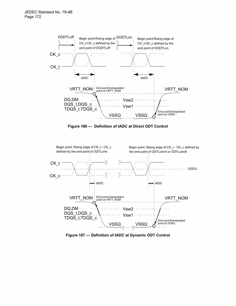
JEDEC Standard No. 79-4BPage 172
Figure 186 — Definition of tADC at Direct ODT Control
Figure 187 — Definition of tADC at Dynamic ODT Control
Begin point:Rising edge of
CK_t-CK_c defined by the
end point of DODTLoff
DODTLoff Begin point:Rising edge of
CK_t-CK_c defined by the
end point of DODTLon
DODTLon
tADC tADC
End point:Extrapolatedpoint at VRTT_NOM
End point:Extrapolatedpoint at VSSQ
VRTT_NOMVRTT_NOM
VSSQ VSSQ
DQ,DMDQS_t,DQS_cTDQS_t,TDQS_c
CK_c
CK_t
Vsw2
Vsw1
tADC tADC
End point:Extrapolatedpoint at VRTT_NOM
End point:Extrapolatedpoint at VSSQ
VRTT_NOMVRTT_NOM
VSSQ VSSQ
DQ,DMDQS_t,DQS_cTDQS_t,TDQS_c
CK_t
CK_c
Vsw2
Vsw1
VDD/2
Begin point: Rising edge of CK_t - CK_c
defined by the end point of ODTLcnw Begin point: Rising edge of CK_t - CK_c defined by
the end point of ODTLcwn4 or ODTLcwn8
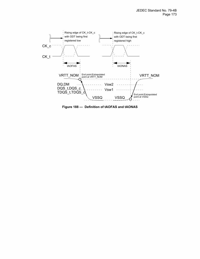
JEDEC Standard No. 79-4B Page 173
Figure 188 — Definition of tAOFAS and tAONAS
Rising edge of CK_t-CK_c
with ODT being first
registered low
Rising edge of CK_t-CK_c
with ODT being first
registered high
tAOFAS tAONAS
End point:Extrapolatedpoint at VRTT_NOM
End point:Extrapolatedpoint at VSSQ
VRTT_NOMVRTT_NOM
VSSQ VSSQ
DQ,DMDQS_t,DQS_cTDQS_t,TDQS_c
CK_c
CK_t
Vsw2
Vsw1
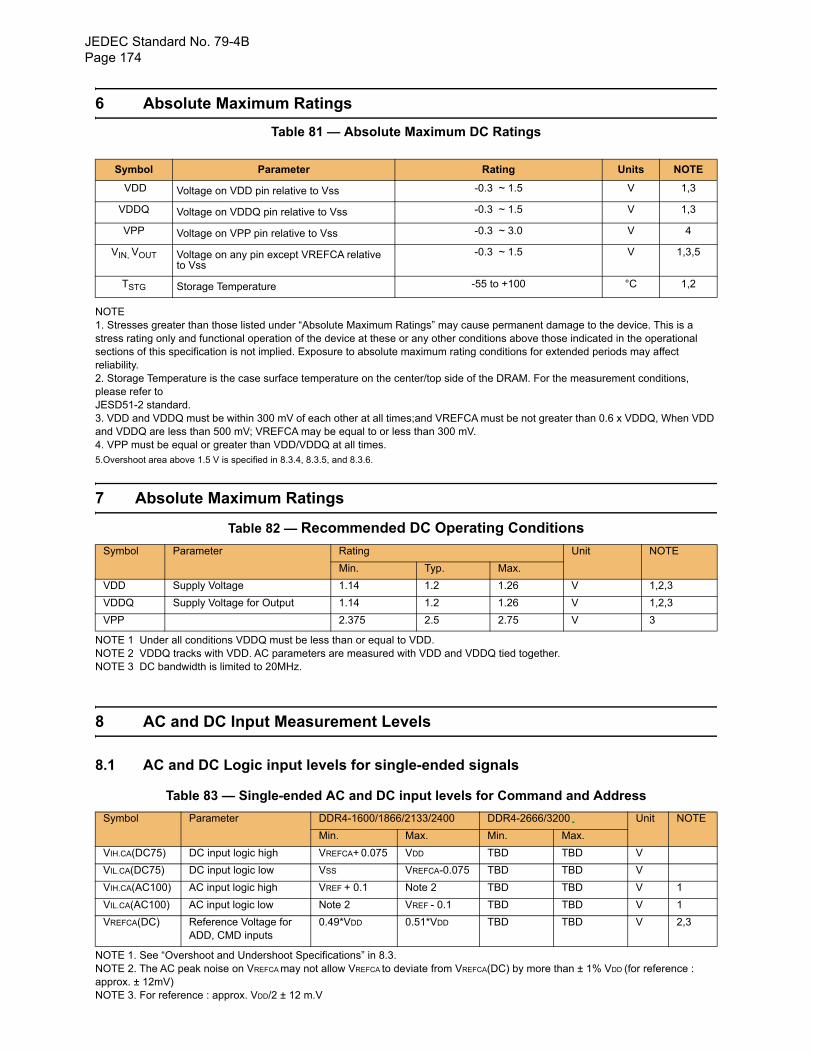
JEDEC Standard No. 79-4BPage 174
6 Absolute Maximum Ratings
Table 81 — Absolute Maximum DC Ratings
NOTE 1. Stresses greater than those listed under “Absolute Maximum Ratings” may cause permanent damage to the device. This is a stress rating only and functional operation of the device at these or any other conditions above those indicated in the operational sections of this specification is not implied. Exposure to absolute maximum rating conditions for extended periods may affect reliability.2. Storage Temperature is the case surface temperature on the center/top side of the DRAM. For the measurement conditions, please refer to JESD51-2 standard.3. VDD and VDDQ must be within 300 mV of each other at all times;and VREFCA must be not greater than 0.6 x VDDQ, When VDD and VDDQ are less than 500 mV; VREFCA may be equal to or less than 300 mV.4. VPP must be equal or greater than VDD/VDDQ at all times.5.Overshoot area above 1.5 V is specified in 8.3.4, 8.3.5, and 8.3.6.
7 Absolute Maximum Ratings
Table 82 — Recommended DC Operating Conditions
NOTE 1 Under all conditions VDDQ must be less than or equal to VDD.NOTE 2 VDDQ tracks with VDD. AC parameters are measured with VDD and VDDQ tied together.NOTE 3 DC bandwidth is limited to 20MHz.
8 AC and DC Input Measurement Levels
8.1 AC and DC Logic input levels for single-ended signals
Table 83 — Single-ended AC and DC input levels for Command and Address
NOTE 1. See “Overshoot and Undershoot Specifications” in 8.3. NOTE 2. The AC peak noise on VREFCA may not allow VREFCA to deviate from VREFCA(DC) by more than ± 1% VDD (for reference : approx. ± 12mV) NOTE 3. For reference : approx. VDD/2 ± 12 m.V
Symbol Parameter Rating Units NOTE
VDD Voltage on VDD pin relative to Vss -0.3 ~ 1.5 V 1,3
VDDQ Voltage on VDDQ pin relative to Vss -0.3 ~ 1.5 V 1,3
VPP Voltage on VPP pin relative to Vss -0.3 ~ 3.0 V 4
VIN, VOUT Voltage on any pin except VREFCA relative to Vss
-0.3 ~ 1.5 V 1,3,5
TSTG Storage Temperature -55 to +100 °C 1,2
Symbol Parameter Rating Unit NOTE
Min. Typ. Max.
VDD Supply Voltage 1.14 1.2 1.26 V 1,2,3
VDDQ Supply Voltage for Output 1.14 1.2 1.26 V 1,2,3
VPP 2.375 2.5 2.75 V 3
Symbol Parameter DDR4-1600/1866/2133/2400 DDR4-2666/3200 Unit NOTE
Min. Max. Min. Max.
VIH.CA(DC75) DC input logic high VREFCA+ 0.075 VDD TBD TBD V
VIL.CA(DC75) DC input logic low VSS VREFCA-0.075 TBD TBD V
VIH.CA(AC100) AC input logic high VREF + 0.1 Note 2 TBD TBD V 1
VIL.CA(AC100) AC input logic low Note 2 VREF - 0.1 TBD TBD V 1
VREFCA(DC) Reference Voltage for ADD, CMD inputs
0.49*VDD 0.51*VDD TBD TBD V 2,3
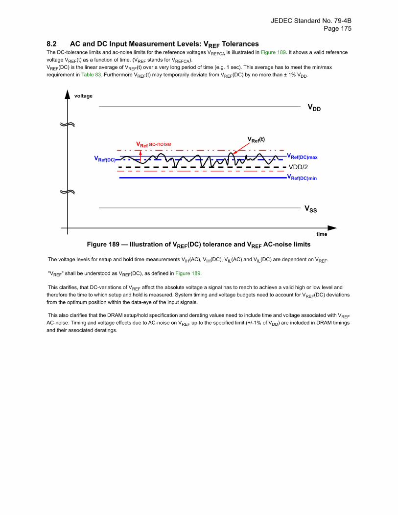
JEDEC Standard No. 79-4B Page 175
8.2 AC and DC Input Measurement Levels: VREF TolerancesThe DC-tolerance limits and ac-noise limits for the reference voltages VREFCA is illustrated in Figure 189. It shows a valid reference
voltage VREF(t) as a function of time. (VREF stands for VREFCA).
VREF(DC) is the linear average of VREF(t) over a very long period of time (e.g. 1 sec). This average has to meet the min/max
requirement in Table 83. Furthermore VREF(t) may temporarily deviate from VREF(DC) by no more than ± 1% VDD.
Figure 189 — Illustration of VREF(DC) tolerance and VREF AC-noise limits
The voltage levels for setup and hold time measurements VIH(AC), VIH(DC), VIL(AC) and VIL(DC) are dependent on VREF.
"VREF" shall be understood as VREF(DC), as defined in Figure 189.
This clarifies, that DC-variations of VREF affect the absolute voltage a signal has to reach to achieve a valid high or low level and
therefore the time to which setup and hold is measured. System timing and voltage budgets need to account for VREF(DC) deviations
from the optimum position within the data-eye of the input signals.
This also clarifies that the DRAM setup/hold specification and derating values need to include time and voltage associated with VREF
AC-noise. Timing and voltage effects due to AC-noise on VREF up to the specified limit (+/-1% of VDD) are included in DRAM timings
and their associated deratings.
VDD
VSS
VRef(t)
VRef(DC)
VRef(DC)min
VDD/2
VRef(DC)max
time
voltage
VRef ac-noise
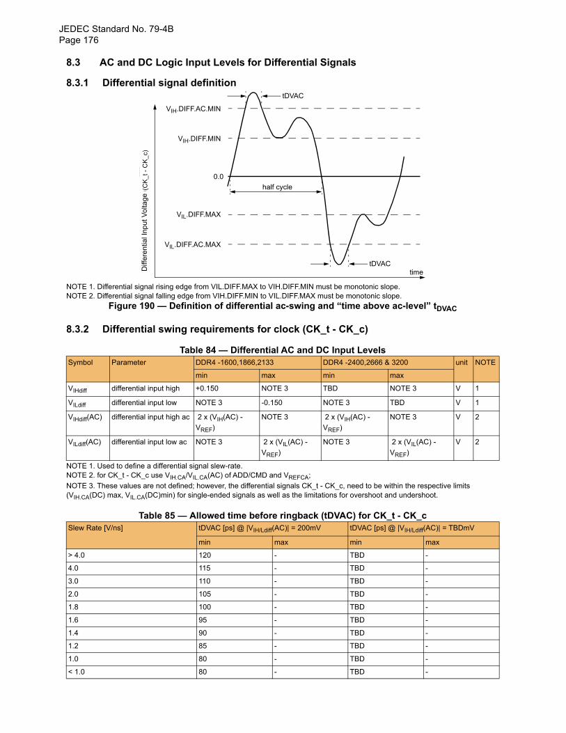
JEDEC Standard No. 79-4BPage 176
8.3 AC and DC Logic Input Levels for Differential Signals
8.3.1 Differential signal definition
0.0
tDVAC
VIH.DIFF.MIN
half cycle
Diff
eren
tial I
nput
Vol
tage
(C
K-C
K)
timetDVAC
VIH.DIFF.AC.MIN
VIL.DIFF.MAX
VIL.DIFF.AC.MAX
(CK
_t -
CK
_c)
NOTE 1. Differential signal rising edge from VIL.DIFF.MAX to VIH.DIFF.MIN must be monotonic slope. NOTE 2. Differential signal falling edge from VIH.DIFF.MIN to VIL.DIFF.MAX must be monotonic slope.
Figure 190 — Definition of differential ac-swing and “time above ac-level” tDVAC
8.3.2 Differential swing requirements for clock (CK_t - CK_c)
Table 84 — Differential AC and DC Input Levels
NOTE 1. Used to define a differential signal slew-rate.NOTE 2. for CK_t - CK_c use VIH.CA/VIL.CA(AC) of ADD/CMD and VREFCA;
NOTE 3. These values are not defined; however, the differential signals CK_t - CK_c, need to be within the respective limits (VIH.CA(DC) max, VIL.CA(DC)min) for single-ended signals as well as the limitations for overshoot and undershoot.
Table 85 — Allowed time before ringback (tDVAC) for CK_t - CK_c
Symbol Parameter DDR4 -1600,1866,2133 DDR4 -2400,2666 & 3200 unit NOTE
min max min max
VIHdiff differential input high +0.150 NOTE 3 TBD NOTE 3 V 1
VILdiff differential input low NOTE 3 -0.150 NOTE 3 TBD V 1
VIHdiff(AC) differential input high ac 2 x (VIH(AC) -
VREF)
NOTE 3 2 x (VIH(AC) -
VREF)
NOTE 3 V 2
VILdiff(AC) differential input low ac NOTE 3 2 x (VIL(AC) -
VREF)
NOTE 3 2 x (VIL(AC) -
VREF)
V 2
Slew Rate [V/ns] tDVAC [ps] @ |VIH/Ldiff(AC)| = 200mV tDVAC [ps] @ |VIH/Ldiff(AC)| = TBDmV
min max min max
> 4.0 120 - TBD -
4.0 115 - TBD -
3.0 110 - TBD -
2.0 105 - TBD -
1.8 100 - TBD -
1.6 95 - TBD -
1.4 90 - TBD -
1.2 85 - TBD -
1.0 80 - TBD -
< 1.0 80 - TBD -
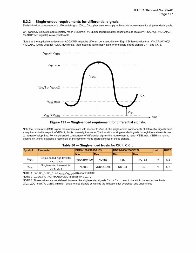
JEDEC Standard No. 79-4B Page 177
8.3.3 Single-ended requirements for differential signalsEach individual component of a differential signal (CK_t, CK_c) has also to comply with certain requirements for single-ended signals.
CK_t and CK_c have to approximately reach VSEHmin / VSELmax (approximately equal to the ac-levels (VIH.CA(AC) / VIL.CA(AC)) for ADD/CMD signals) in every half-cycle.
Note that the applicable ac-levels for ADD/CMD might be different per speed-bin etc. E.g., if Different value than VIH.CA(AC100)/VIL.CA(AC100) is used for ADD/CMD signals, then these ac-levels apply also for the single-ended signals CK_t and CK_c.
Figure 191 — Single-ended requirement for differential signals.
Note that, while ADD/CMD signal requirements are with respect to VrefCA, the single-ended components of differential signals have a requirement with respect to VDD / 2; this is nominally the same. The transition of single-ended signals through the ac-levels is used to measure setup time. For single-ended components of differential signals the requirement to reach VSELmax, VSEHmin has no bearing on timing, but adds a restriction on the common mode characteristics of these signals.
Table 86 — Single-ended levels for CK_t, CK_c
NOTE 1 For CK_t - CK_c use VIH.CA/VIL.CA(AC) of ADD/CMD;
NOTE 2 VIH(AC)/VIL(AC) for ADD/CMD is based on VREFCA;
NOTE 3 These values are not defined, however the single-ended signals CK_t - CK_c need to be within the respective limits (VIH.CA(DC) max, VIL.CA(DC)min) for single-ended signals as well as the limitations for overshoot and undershoot.
Symbol Parameter DDR4-1600/1866/2133 DDR4-2400/2666/3200 Unit NOTE
Min Max Min Max
VSEHSingle-ended high-level for
CK_t , CK_c(VDD/2)+0.100 NOTE3 TBD NOTE3 V 1, 2
VSELSingle-ended low-level for
CK_t , CK_cNOTE3 (VDD/2)-0.100 NOTE3 TBD V 1, 2
VDD or VDDQ
VSEH min
VDD/2 or VDDQ/2
VSEL max
VSEH
VSS or VSSQ
VSEL
CK
time
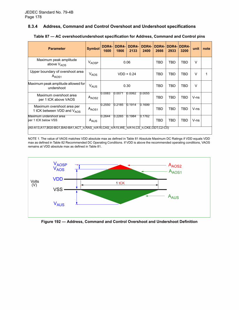
JEDEC Standard No. 79-4BPage 178
8.3.4 Address, Command and Control Overshoot and Undershoot specifications
Table 87 — AC overshoot/undershoot specification for Address, Command and Control pins
NOTE 1. The value of VAOS matches VDD absolute max as defined in Table 81 Absolute Maximum DC Ratings if VDD equals VDD max as defined in Table 82 Recommended DC Operating Conditions. If VDD is above the recommended operating conditions, VAOS remains at VDD absolute max as defined in Table 81.
Figure 192 — Address, Command and Control Overshoot and Undershoot Definition
Parameter SymbolDDR4-1600
DDR4-1866
DDR4-2133
DDR4-2400
DDR4-2666
DDR4-2933
DDR4-3200
unit note
Maximum peak amplitude above VAOS
VAOSP 0.06 TBD TBD TBD V
Upper boundary of overshoot area AAOS1
VAOS VDD + 0.24 TBD TBD TBD V 1
Maximum peak amplitude allowed for undershoot
VAUS 0.30 TBD TBD TBD V
Maximum overshoot area per 1 tCK above VAOS
AAOS2
0.0083 0.0071 0.0062 0.0055TBD TBD TBD V-ns
Maximum overshoot area per 1 tCK between VDD and VAOS
AAOS1
0.2550 0.2185 0.1914 0.1699TBD TBD TBD V-ns
Maximum undershoot area per 1 tCK below VSS AAUS
0.2644 0.2265 0.1984 0.1762TBD TBD TBD V-ns
(A0-A13,A17,BG0-BG1,BA0-BA1,ACT_n,RAS_n/A16,CAS_n/A15,WE_n/A14,CS_n,CKE,ODT,C2-C0)
VDD
VSS
Volts(V) 1 tCK
AAOS1
VAOSPVAOS
VAUS
AAOS2
AAUS
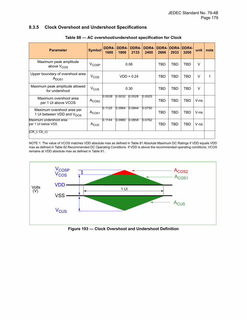
JEDEC Standard No. 79-4B Page 179
8.3.5 Clock Overshoot and Undershoot Specifications
Table 88 — AC overshoot/undershoot specification for Clock
NOTE 1. The value of VCOS matches VDD absolute max as defined in Table 81 Absolute Maximum DC Ratings if VDD equals VDD max as defined in Table 82 Recommended DC Operating Conditions. If VDD is above the recommended operating conditions, VCOS remains at VDD absolute max as defined in Table 81.
Figure 193 — Clock Overshoot and Undershoot Definition
Parameter SymbolDDR4-1600
DDR4-1866
DDR4-2133
DDR4-2400
DDR4-2666
DDR4-2933
DDR4-3200
unit note
Maximum peak amplitude above VCOS
VCOSP 0.06 TBD TBD TBD V
Upper boundary of overshoot area ADOS1
VCOS VDD + 0.24 TBD TBD TBD V 1
Maximum peak amplitude allowed for undershoot
VCUS 0.30 TBD TBD TBD V
Maximum overshoot area per 1 UI above VCOS
ACOS2
0.0038 0.0032 0.0028 0.0025TBD TBD TBD V-ns
Maximum overshoot area per 1 UI between VDD and VDOS
ACOS1
0.1125 0.0964 0.0844 0.0750TBD TBD TBD V-ns
Maximum undershoot area per 1 UI below VSS ACUS
0.1144 0.0980 0.0858 0.0762TBD TBD TBD V-ns
(CK_t, Ck_c)
VDD
VSS
Volts(V) 1 UI
ACOS1
VCOSPVCOS
VCUS
ACOS2
ACUS
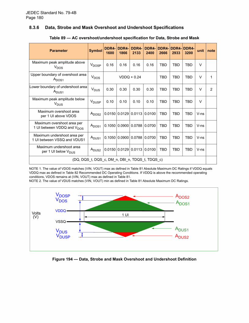
JEDEC Standard No. 79-4BPage 180
8.3.6 Data, Strobe and Mask Overshoot and Undershoot Specifications
Table 89 — AC overshoot/undershoot specification for Data, Strobe and Mask
NOTE 1. The value of VDOS matches (VIN, VOUT) max as defined in Table 81 Absolute Maximum DC Ratings if VDDQ equals VDDQ max as defined in Table 82 Recommended DC Operating Conditions. If VDDQ is above the recommended operating conditions, VDOS remains at (VIN, VOUT) max as defined in Table 81.NOTE 2. The value of VDUS matches (VIN, VOUT) min as defined in Table 81 Absolute Maximum DC Ratings.
Figure 194 — Data, Strobe and Mask Overshoot and Undershoot Definition
Parameter SymbolDDR4-1600
DDR4-1866
DDR4-2133
DDR4-2400
DDR4-2666
DDR4-2933
DDR4-3200
unit note
Maximum peak amplitude above VDOS
VDOSP 0.16 0.16 0.16 0.16 TBD TBD TBD V
Upper boundary of overshoot area ADOS1
VDOS VDDQ + 0.24 TBD TBD TBD V 1
Lower boundary of undershoot area ADUS1
VDUS 0.30 0.30 0.30 0.30 TBD TBD TBD V 2
Maximum peak amplitude below VDUS
VDUSP 0.10 0.10 0.10 0.10 TBD TBD TBD V
Maximum overshoot area per 1 UI above VDOS
ADOS2 0.0150 0.0129 0.0113 0.0100 TBD TBD TBD V-ns
Maximum overshoot area per 1 UI between VDDQ and VDOS
ADOS1 0.1050 0.0900 0.0788 0.0700 TBD TBD TBD V-ns
Maximum undershoot area per 1 UI between VSSQ and VDUS1
ADUS1 0.1050 0.0900 0.0788 0.0700 TBD TBD TBD V-ns
Maximum undershoot area per 1 UI below VDUS
ADUS2 0.0150 0.0129 0.0113 0.0100 TBD TBD TBD V-ns
(DQ, DQS_t, DQS_c, DM_n, DBI_n, TDQS_t, TDQS_c)
VDDQ
VSSQ
Volts(V) 1 UI
ADOS1
VDOSPVDOS
VDUSVDUSP
ADOS2
ADUS1
ADUS2
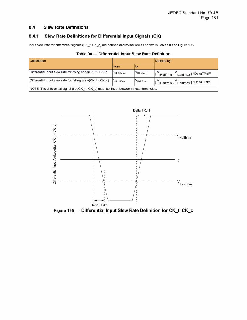
JEDEC Standard No. 79-4B Page 181
8.4 Slew Rate Definitions
8.4.1 Slew Rate Definitions for Differential Input Signals (CK)
Input slew rate for differential signals (CK_t, CK_c) are defined and measured as shown in Table 90 and Figure 195.
Table 90 — Differential Input Slew Rate Definition
Figure 195 — Differential Input Slew Rate Definition for CK_t, CK_c
Description Defined by
from to
Differential input slew rate for rising edge(CK_t - CK_c) VILdiffmax VIHdiffmin VIHdiffmin - V
ILdiffmax DeltaTRdiff
Differential input slew rate for falling edge(CK_t - CK_c) VIHdiffmin VILdiffmax VIHdiffmin - V
ILdiffmax DeltaTFdiff
NOTE: The differential signal (i,e.,CK_t - CK_c) must be linear between these thresholds.
Delta TRdiff
Delta TFdiff
VIHdiffmin
0
VILdiffmaxD
iffer
entia
l Inp
ut V
olta
ge(i
,e, C
K_t
- C
K_c
)
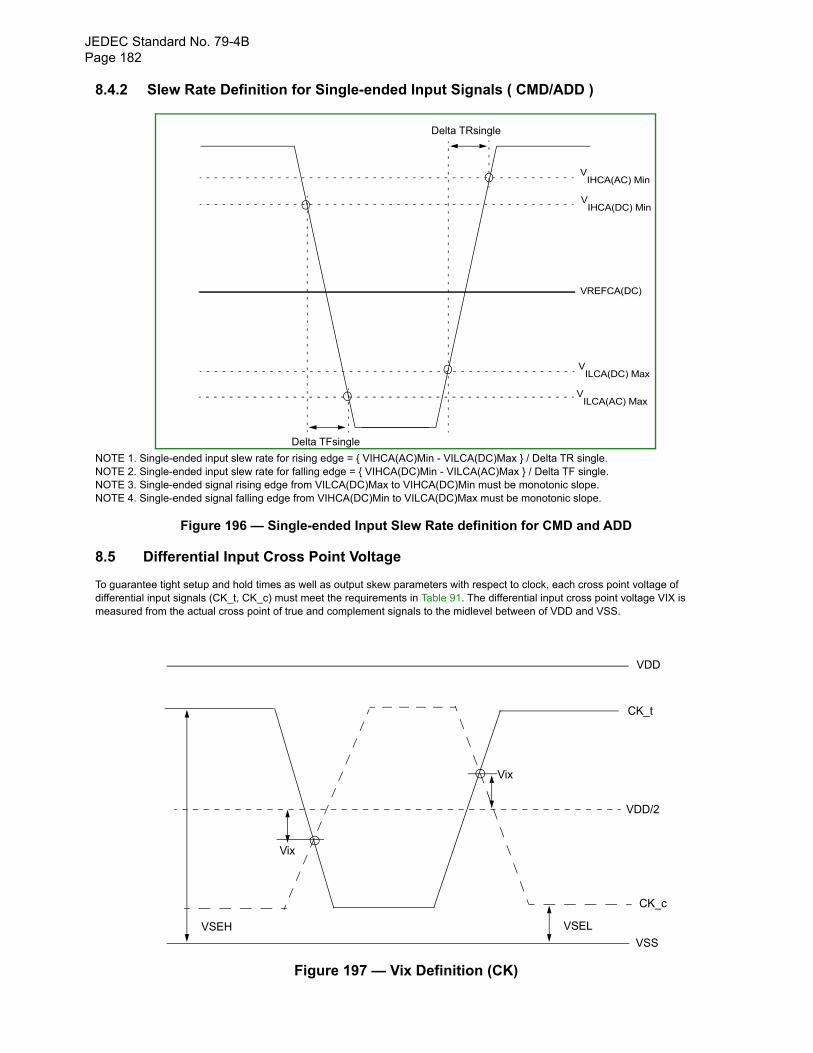
JEDEC Standard No. 79-4BPage 182
8.4.2 Slew Rate Definition for Single-ended Input Signals ( CMD/ADD )
NOTE 1. Single-ended input slew rate for rising edge = { VIHCA(AC)Min - VILCA(DC)Max } / Delta TR single.NOTE 2. Single-ended input slew rate for falling edge = { VIHCA(DC)Min - VILCA(AC)Max } / Delta TF single.NOTE 3. Single-ended signal rising edge from VILCA(DC)Max to VIHCA(DC)Min must be monotonic slope.NOTE 4. Single-ended signal falling edge from VIHCA(DC)Min to VILCA(DC)Max must be monotonic slope.
Figure 196 — Single-ended Input Slew Rate definition for CMD and ADD
8.5 Differential Input Cross Point Voltage
To guarantee tight setup and hold times as well as output skew parameters with respect to clock, each cross point voltage of differential input signals (CK_t, CK_c) must meet the requirements in Table 91. The differential input cross point voltage VIX is measured from the actual cross point of true and complement signals to the midlevel between of VDD and VSS.
Figure 197 — Vix Definition (CK)
Delta TRsingle
Delta TFsingle
VIHCA(AC) Min
VIHCA(DC) Min
VREFCA(DC)
VILCA(DC) Max
VILCA(AC) Max
Vix
CK_t
VDD/2
VSS
VDD
CK_c
Vix
VSELVSEH
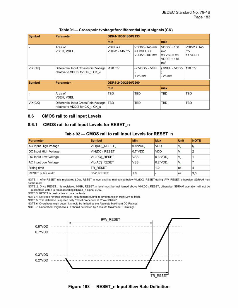
JEDEC Standard No. 79-4B Page 183
Table 91 — Cross point voltage for differential input signals (CK)
8.6 CMOS rail to rail Input Levels
8.6.1 CMOS rail to rail Input Levels for RESET_n
Table 92 — CMOS rail to rail Input Levels for RESET_n
NOTE 1. After RESET_n is registered LOW, RESET_n level shall be maintained below VIL(DC)_RESET during tPW_RESET, otherwise, SDRAM may not be reset.NOTE 2. Once RESET_n is registered HIGH, RESET_n level must be maintained above VIH(DC)_RESET, otherwise, SDRAM operation will not be
guaranteed until it is reset asserting RESET_n signal LOW.NOTE 3. RESET is destructive to data contents.NOTE 4. No slope reversal (ringback) requirement during its level transition from Low to High.NOTE 5. This definition is applied only “Reset Procedure at Power Stable”.NOTE 6. Overshoot might occur. It should be limited by the Absolute Maximum DC Ratings.NOTE 7. Undershoot might occur. It should be limited by Absolute Maximum DC Ratings
Figure 198 — RESET_n Input Slew Rate Definition
Symbol Parameter DDR4-1600/1866/2133
min max
- Area ofVSEH, VSEL
VSEL =<VDD/2 - 145 mV
VDD/2 - 145 mV=< VSEL =<VDD/2 - 100 mV
VDD/2 + 100 mV=< VSEH =<VDD/2 + 145 mV
VDD/2 + 145 mV=< VSEH
VlX(CK) Differential Input Cross Point Voltage relative to VDD/2 for CK_t, CK_c
-120 mV - ( VDD/2 - VSEL )+ 25 mV
( VSEH - VDD/2 )- 25 mV
120 mV
Symbol Parameter DDR4-2400/2666/3200
min max
- Area ofVSEH, VSEL
TBD TBD TBD TBD
VlX(CK) Differential Input Cross Point Voltage relative to VDD/2 for CK_t, CK_c
TBD TBD TBD TBD
Parameter Symbol Min Max Unit NOTE
AC Input High Voltage VIH(AC)_RESET 0.8*VDD VDD V 6
DC Input High Voltage VIH(DC)_RESET 0.7*VDD VDD V 2
DC Input Low Voltage VIL(DC)_RESET VSS 0.3*VDD V 1
AC Input Low Voltage VIL(AC)_RESET VSS 0.2*VDD V 7
Rising time TR_RESET - 1.0 us 4
RESET pulse width tPW_RESET 1.0 - us 3,5
0.8*VDD
TR_RESET
tPW_RESET
0.7*VDD
0.3*VDD
0.2*VDD
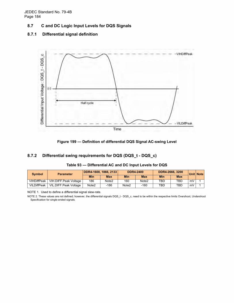
JEDEC Standard No. 79-4BPage 184
8.7 C and DC Logic Input Levels for DQS Signals
8.7.1 Differential signal definition
Figure 199 — Definition of differential DQS Signal AC-swing Level
8.7.2 Differential swing requirements for DQS (DQS_t - DQS_c)
Table 93 — Differential AC and DC Input Levels for DQS
NOTE 1. Used to define a differential signal slew-rate.NOTE 2. These values are not defined; however, the differential signals DQS_t - DQS_c, need to be within the respective limits Overshoot, Undershoot
Specification for single-ended signals.
Symbol ParameterDDR4-1600, 1866, 2133 DDR4-2400 DDR4-2666, 3200
Unit NoteMin Max Min Max Min Max
VIHDiffPeak VIH.DIFF.Peak Voltage 186 Note2 160 Note2 TBD TBD mV 1
VILDiffPeak VIL.DIFF.Peak Voltage Note2 -186 Note2 -160 TBD TBD mV 1
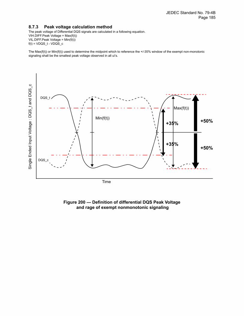
JEDEC Standard No. 79-4B Page 185
8.7.3 Peak voltage calculation methodThe peak voltage of Differential DQS signals are calculated in a following equation.VIH.DIFF.Peak Voltage = Max(f(t))VIL.DIFF.Peak Voltage = Min(f(t))f(t) = VDQS_t - VDQS_c
The Max(f(t)) or Min(f(t)) used to determine the midpoint which to reference the +/-35% window of the exempt non-monotonic signaling shall be the smallest peak voltage observed in all ui’s.
Figure 200 — Definition of differential DQS Peak Voltage and rage of exempt nonmonotonic signaling
DQS_t
DQS_c
Sin
gle
En
ded
In
put
Vo
ltag
e :
DQ
S_t
an
d D
QS
_c
Min(f(t))
+35%
+35%
+50%
+50%
Time
Max(f(t))
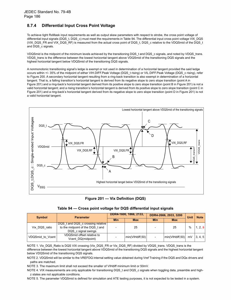
JEDEC Standard No. 79-4BPage 186
8.7.4 Differential Input Cross Point Voltage
To achieve tight RxMask input requirements as well as output skew parameters with respect to strobe, the cross point voltage of differential input signals (DQS_t, DQS_c) must meet the requirements in Table 94. The differential input cross point voltage VIX_DQS (VIX_DQS_FR and VIX_DQS_RF) is measured from the actual cross point of DQS_t, DQS_c relative to the VDQSmid of the DQS_t and DQS_c signals.
VDQSmid is the midpoint of the minimum levels achieved by the transitioning DQS_t and DQS_c signals, and noted by VDQS_trans. VDQS_trans is the difference between the lowest horizontal tangent above VDQSmid of the transitioning DQS signals and the highest horizontal tangent below VDQSmid of the transitioning DQS signals.
A nonmonotonic transitioning signal’s ledge is exempt or not used in determination of a horizontal tangent provided the said ledge occurs within +/- 35% of the midpoint of either VIH.DIFF.Peak Voltage (DQS_t rising) or VIL.DIFF.Peak Voltage (DQS_c rising), refer to Figure 200. A secondary horizontal tangent resulting from a ring-back transition is also exempt in determination of a horizontal tangent. That is, a falling transition’s horizontal tangent is derived from its negative slope to zero slope transition (point A in Figure 201) and a ring-back’s horizontal tangent derived from its positive slope to zero slope transition (point B in Figure 201) is not a valid horizontal tangent; and a rising transition’s horizontal tangent is derived from its positive slope to zero slope transition (point C in Figure 201) and a ring-back’s horizontal tangent derived from its negative slope to zero slope transition (point D in Figure 201) is not a valid horizontal tangent.
C
D
B
A
VIX_DQS,RF
VIX_DQS,FR
VIX_DQS,FR
VIX_DQS,RF
DQS_t
VDQSmid
DQS_c
Lowest horizontal tangent above VDQSmid of the transitioning signals
DQ
S_t,D
QS
_c : S
ingle
-ended Input V
oltages
VSSQ
Highest horizontal tanget below VDQSmid of the transitioning signals
VD
QS
_tr
an
s/2
VD
QS
_tr
an
sFigure 201 — Vix Definition (DQS)
Table 94 — Cross point voltage for DQS differential input signals
NOTE 1. Vix_DQS_Ratio is DQS VIX crossing (Vix_DQS_FR or Vix_DQS_RF) divided by VDQS_trans. VDQS_trans is the difference between the lowest horizontal tangent above VDQSmid of the transitioning DQS signals and the highest horizontal tangent below VDQSmid of the transitioning DQS signals.
NOTE 2. VDQSmid will be similar to the VREFDQ internal setting value obtained during Vref Training if the DQS and DQs drivers and paths are matched.
NOTE 3. The maximum limit shall not exceed the smaller of VIHdiff minimum limit or 50mV.NOTE 4. VIX measurements are only applicable for transitioning DQS_t and DQS_c signals when toggling data, preamble and high-
z states are not applicable conditions.NOTE 5. The parameter VDQSmid is defined for simulation and ATE testing purposes, it is not expected to be tested in a system.
Symbol ParameterDDR4-1600, 1866, 2133, DDR4-2666, 2933, 3200
Unit NoteMin Max Min Max
Vix_DQS_ratioDQS_t and DQS_c crossing relative
to the midpoint of the DQS_t and DQS_c signal swings
- 25 - 25 % 1, 2, 3
VDQSmid_to_VcentVDQSmid offset relative to
Vcent_DQ(midpoint)- min(VIHdiff,50) - min(VIHdiff,50) mV 3, 4, 5
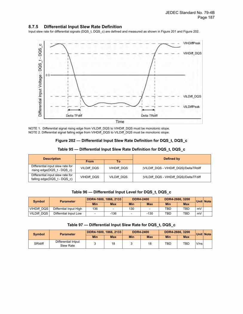
JEDEC Standard No. 79-4B Page 187
8.7.5 Differential Input Slew Rate DefinitionInput slew rate for differential signals (DQS_t, DQS_c) are defined and measured as shown in Figure 201 and Figure 202.
NOTE 1. Differential signal rising edge from VILDiff_DQS to VIHDiff_DQS must be monotonic slope.NOTE 2. Differential signal falling edge from VIHDiff_DQS to VILDiff_DQS must be monotonic slope.
Figure 202 — Differential Input Slew Rate Definition for DQS_t, DQS_c
Table 95 — Differential Input Slew Rate Definition for DQS_t, DQS_c
Table 96 — Differential Input Level for DQS_t, DQS_c
Table 97 — Differential Input Slew Rate for DQS_t, DQS_c
Description Defined byFrom To
Differential input slew rate forrising edge(DQS_t - DQS_c)
VILDiff_DQS VIHDiff_DQS |VILDiff_DQS - VIHDiff_DQS|/DeltaTRdiff
Differential input slew rate forfalling edge(DQS_t - DQS_c)
VIHDiff_DQS VILDiff_DQS |VILDiff_DQS - VIHDiff_DQS|/DeltaTFdiff
Symbol ParameterDDR4-1600, 1866, 2133 DDR4-2400 DDR4-2666, 3200
Unit NoteMin Max Min Max Min Max
VIHDiff_DQS Differntial Input High 136 - 130 - TBD TBD mV
VILDiff_DQS Differntial Input Low - -136 - -130 TBD TBD mV
Symbol ParameterDDR4-1600, 1866, 2133 DDR4-2400 DDR4-2666, 3200
Unit NoteMin Max Min Max Min Max
SRIdiffDifferential Intput
Slew Rate3 18 3 18 TBD TBD V/ns
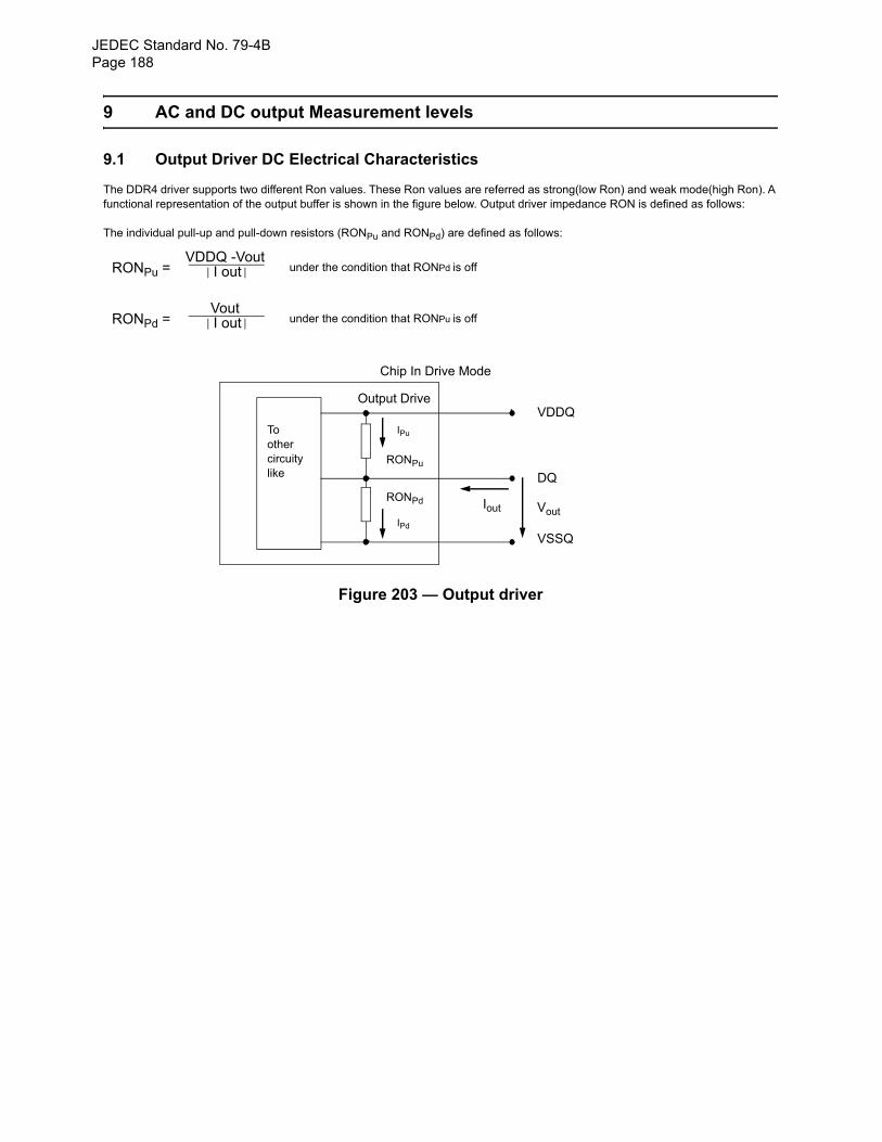
JEDEC Standard No. 79-4BPage 188
9 AC and DC output Measurement levels
9.1 Output Driver DC Electrical Characteristics
The DDR4 driver supports two different Ron values. These Ron values are referred as strong(low Ron) and weak mode(high Ron). A functional representation of the output buffer is shown in the figure below. Output driver impedance RON is defined as follows:
The individual pull-up and pull-down resistors (RONPu and RONPd) are defined as follows:
Figure 203 — Output driver
RONPu = VDDQ -Vout
I out under the condition that RONPd is off
RONPd = VoutI out under the condition that RONPu is off
Toothercircuitylike
Output Drive
DQ
RONPu
VSSQ
VDDQ
Iout Vout
Chip In Drive Mode
RONPd
IPu
IPd
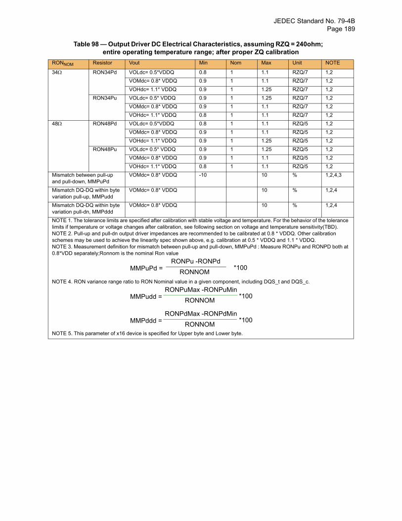
JEDEC Standard No. 79-4B Page 189
Table 98 — Output Driver DC Electrical Characteristics, assuming RZQ = 240ohm; entire operating temperature range; after proper ZQ calibration
RONNOM Resistor Vout Min Nom Max Unit NOTE
34 RON34Pd VOLdc= 0.5*VDDQ 0.8 1 1.1 RZQ/7 1,2
VOMdc= 0.8* VDDQ 0.9 1 1.1 RZQ/7 1,2
VOHdc= 1.1* VDDQ 0.9 1 1.25 RZQ/7 1,2
RON34Pu VOLdc= 0.5* VDDQ 0.9 1 1.25 RZQ/7 1,2
VOMdc= 0.8* VDDQ 0.9 1 1.1 RZQ/7 1,2
VOHdc= 1.1* VDDQ 0.8 1 1.1 RZQ/7 1,2
48 RON48Pd VOLdc= 0.5*VDDQ 0.8 1 1.1 RZQ/5 1,2
VOMdc= 0.8* VDDQ 0.9 1 1.1 RZQ/5 1,2
VOHdc= 1.1* VDDQ 0.9 1 1.25 RZQ/5 1,2
RON48Pu VOLdc= 0.5* VDDQ 0.9 1 1.25 RZQ/5 1,2
VOMdc= 0.8* VDDQ 0.9 1 1.1 RZQ/5 1,2
VOHdc= 1.1* VDDQ 0.8 1 1.1 RZQ/5 1,2
Mismatch between pull-up and pull-down, MMPuPd
VOMdc= 0.8* VDDQ -10 10 % 1,2,4,3
Mismatch DQ-DQ within byte variation pull-up, MMPudd
VOMdc= 0.8* VDDQ 10 % 1,2,4
Mismatch DQ-DQ within byte variation pull-dn, MMPddd
VOMdc= 0.8* VDDQ 10 % 1,2,4
NOTE 1. The tolerance limits are specified after calibration with stable voltage and temperature. For the behavior of the tolerance limits if temperature or voltage changes after calibration, see following section on voltage and temperature sensitivity(TBD). NOTE 2. Pull-up and pull-dn output driver impedances are recommended to be calibrated at 0.8 * VDDQ. Other calibration schemes may be used to achieve the linearity spec shown above, e.g. calibration at 0.5 * VDDQ and 1.1 * VDDQ. NOTE 3. Measurement definition for mismatch between pull-up and pull-down, MMPuPd : Measure RONPu and RONPD both at 0.8*VDD separately;Ronnom is the nominal Ron value
NOTE 4. RON variance range ratio to RON Nominal value in a given component, including DQS_t and DQS_c.
NOTE 5. This parameter of x16 device is specified for Upper byte and Lower byte.
MMPuPd = RONPu -RONPd
RONNOM*100
MMPudd = RONPuMax -RONPuMin
RONNOM*100
MMPddd = RONPdMax -RONPdMin
RONNOM*100
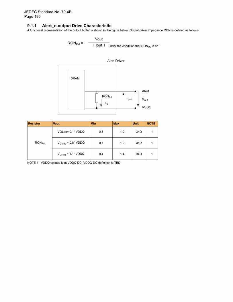
JEDEC Standard No. 79-4BPage 190
9.1.1 Alert_n output Drive CharacteristicA functional representation of the output buffer is shown in the figure below. Output driver impedance RON is defined as follows:
NOTE 1 VDDQ voltage is at VDDQ DC. VDDQ DC definition is TBD.
Resistor Vout Min Max Unit NOTE
RONPd
VOLdc= 0.1* VDDQ 0.3 1.2 34Ω 1
VOMdc = 0.8* VDDQ 0.4 1.2 34Ω 1
VOHdc = 1.1* VDDQ 0.4 1.4 34Ω 1
RONPd = Vout
l Iout l under the condition that RONPu is off
DRAM
Alert
VSSQ
Iout VoutRONPd
IPd
Alert Driver
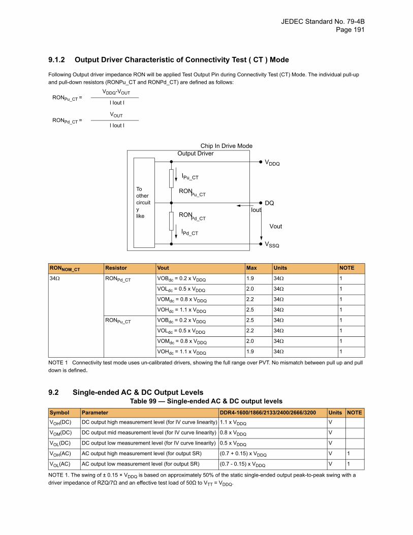
JEDEC Standard No. 79-4B Page 191
9.1.2 Output Driver Characteristic of Connectivity Test ( CT ) Mode
Following Output driver impedance RON will be applied Test Output Pin during Connectivity Test (CT) Mode. The individual pull-up
and pull-down resistors (RONPu_CT and RONPd_CT) are defined as follows:
NOTE 1 Connectivity test mode uses un-calibrated drivers, showing the full range over PVT. No mismatch between pull up and pull
down is defined.
9.2 Single-ended AC & DC Output LevelsTable 99 — Single-ended AC & DC output levels
NOTE 1. The swing of ± 0.15 × VDDQ is based on approximately 50% of the static single-ended output peak-to-peak swing with a
driver impedance of RZQ/7Ω and an effective test load of 50Ω to VTT = VDDQ.
RONNOM_CT Resistor Vout Max Units NOTE
34 RONPd_CT VOBdc = 0.2 x VDDQ 1.9 34 1
VOLdc = 0.5 x VDDQ 2.0 34 1
VOMdc = 0.8 x VDDQ 2.2 34 1
VOHdc = 1.1 x VDDQ 2.5 34 1
RONPu_CT VOBdc = 0.2 x VDDQ 2.5 34 1
VOLdc = 0.5 x VDDQ 2.2 34 1
VOMdc = 0.8 x VDDQ 2.0 34 1
VOHdc = 1.1 x VDDQ 1.9 34 1
Symbol Parameter DDR4-1600/1866/2133/2400/2666/3200 Units NOTE
VOH(DC) DC output high measurement level (for IV curve linearity) 1.1 x VDDQ V
VOM(DC) DC output mid measurement level (for IV curve linearity) 0.8 x VDDQ V
VOL(DC) DC output low measurement level (for IV curve linearity) 0.5 x VDDQ V
VOH(AC) AC output high measurement level (for output SR) (0.7 + 0.15) x VDDQ V 1
VOL(AC) AC output low measurement level (for output SR) (0.7 - 0.15) x VDDQ V 1
RONPu_CT =VDDQ-VOUT
l Iout l
RONPd_CT =VOUT
l Iout l
VDDQ
DQ
VSSQ
RONPu_CT
IPd_CT
RONPd_CT
Toothercircuitylike
Output Driver
IPu_CT
Iout
Vout
Chip In Drive Mode
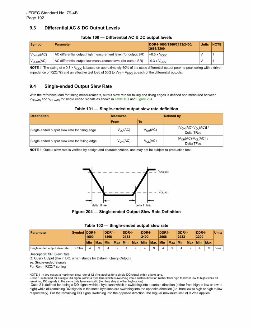
JEDEC Standard No. 79-4BPage 192
9.3 Differential AC & DC Output Levels
Table 100 — Differential AC & DC output levels
NOTE 1. The swing of ± 0.3 × VDDQ is based on approximately 50% of the static differential output peak-to-peak swing with a driver
impedance of RZQ/7Ω and an effective test load of 50Ω to VTT = VDDQ at each of the differential outputs.
9.4 Single-ended Output Slew Rate
With the reference load for timing measurements, output slew rate for falling and rising edges is defined and measured between VOL(AC) and VOH(AC) for single ended signals as shown in Table 101 and Figure 204.
Table 101 — Single-ended output slew rate definition
NOTE 1. Output slew rate is verified by design and characterization, and may not be subject to production test.
Figure 204 — Single-ended Output Slew Rate Definition
Table 102 — Single-ended output slew rate
Description: SR: Slew RateQ: Query Output (like in DQ, which stands for Data-in, Query-Output)se: Single-ended SignalsFor Ron = RZQ/7 setting
NOTE 1 In two cases, a maximum slew rate of 12 V/ns applies for a single DQ signal within a byte lane.-Case 1 is defined for a single DQ signal within a byte lane which is switching into a certain direction (either from high to low or low to high) while all remaining DQ signals in the same byte lane are static (i.e. they stay at either high or low).-Case 2 is defined for a single DQ signal within a byte lane which is switching into a certain direction (either from high to low or low to high) while all remaining DQ signals in the same byte lane are switching into the opposite direction (i.e. from low to high or high to low respectively). For the remaining DQ signal switching into the opposite direction, the regular maximum limit of 9 V/ns applies
Symbol Parameter DDR4-1600/1866/2133/2400/2666/3200
Units NOTE
VOHdiff(AC) AC differential output high measurement level (for output SR) +0.3 x VDDQ V 1
VOLdiff(AC) AC differential output low measurement level (for output SR) -0.3 x VDDQ V 1
Description Measured Defined by
From To
Single ended output slew rate for rising edge VOL(AC) VOH(AC) [VOH(AC)-VOL(AC)] /
Delta TRse
Single ended output slew rate for falling edge VOH(AC) VOL(AC)[VOH(AC)-VOL(AC)] /
Delta TFse
Parameter Symbol DDR4-1600
DDR4-1866
DDR4-2133
DDR4-2400
DDR4-2666
DDR4-2933
DDR4-3200
Units
Min Max Min Max Min Max Min Max Min Max Min Max Min Max
Single ended output slew rate SRQse 4 9 4 9 4 9 4 9 4 9 4 9 4 9 V/ns
VOH(AC)
VOL(AC)
delta TRsedelta TFse
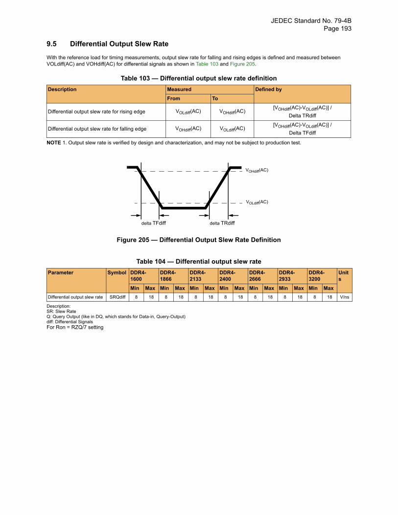
JEDEC Standard No. 79-4B Page 193
9.5 Differential Output Slew Rate
With the reference load for timing measurements, output slew rate for falling and rising edges is defined and measured between VOLdiff(AC) and VOHdiff(AC) for differential signals as shown in Table 103 and Figure 205.
Table 103 — Differential output slew rate definition
NOTE 1. Output slew rate is verified by design and characterization, and may not be subject to production test.
Figure 205 — Differential Output Slew Rate Definition
Table 104 — Differential output slew rate
Description:SR: Slew RateQ: Query Output (like in DQ, which stands for Data-in, Query-Output)diff: Differential SignalsFor Ron = RZQ/7 setting
Description Measured Defined by
From To
Differential output slew rate for rising edge VOLdiff(AC) VOHdiff(AC)[VOHdiff(AC)-VOLdiff(AC)] /
Delta TRdiff
Differential output slew rate for falling edge VOHdiff(AC) VOLdiff(AC)[VOHdiff(AC)-VOLdiff(AC)] /
Delta TFdiff
Parameter Symbol DDR4-1600
DDR4-1866
DDR4-2133
DDR4-2400
DDR4-2666
DDR4-2933
DDR4-3200
Units
Min Max Min Max Min Max Min Max Min Max Min Max Min Max
Differential output slew rate SRQdiff 8 18 8 18 8 18 8 18 8 18 8 18 8 18 V/ns
VOHdiff(AC)
VOLdiff(AC)
delta TRdiffdelta TFdiff
JEDEC Standard No. 79-4BPage 194
9.6 Single-ended AC and DC Output Levels of Connectivity Test Mode
Following output parameters will be applied for DDR4 SDRAM Output Signal during Connectivity Test Mode.
Table 105 — Single-ended AC & DC output levels of Connectivity Test Mode
NOTE 1. The effective test load is 50Ω terminated by VTT = 0.5 * VDDQ.
Figure 206 — Output Slew Rate Definition of Connectivity Test Mode
Table 106 — Single-ended output slew rate of Connectivity Test Mode
9.7 Test Load for Connectivity Test Mode Timing
The reference load for ODT timings is defined in Figure 207.
Figure 207 — Connectivity Test Mode Timing Reference Load
Symbol Parameter DDR4-1600/1866/2133/ 2400/2666/3200
Unit Notes
VOH(DC) DC output high measurement level (for IV curve linearity) 1.1 x VDDQ V
VOM(DC) DC output mid measurement level (for IV curve linearity) 0.8 x VDDQ V
VOL(DC) DC output low measurement level (for IV curve linearity) 0.5 x VDDQ V
VOB(DC) DC output below measurement level (for IV curve linearity) 0.2 x VDDQ V
VOH(AC) AC output high measurement level (for output SR) VTT + (0.1 x VDDQ) V 1
VOL(AC) AC output below measurement level (for output SR) VTT - (0.1 x VDDQ) V 1
Parameter Symbol DDR4-1600/1866/2133/ 2400/2666/3200 Unit Notes
Min Max
Output signal Falling time TF_output_CT - 10 ns/V
Output signal Rising time TR_output_CT - 10 ns/V
VOH(AC)
TR_output_CT
VTT 0.5 * VDDQ
VOL(AC)
TF_output_CT
VDDQ
CT_INPUTSDUT
DQ, DM
DQSU_t , DQSU_cDQS_t , DQS_c
Rterm = 50 ohm
Timing Reference Points
VSSQ
DQSL_t , DQSL_c
0.5*VDDQ
JEDEC Standard No. 79-4B Page 195
10 Speed Bin
Table 107 — DDR4-1600 Speed Bins and Operations
Speed Bin DDR4-1600J DDR4-1600K DDR4-1600L Unit NOTE
CL-nRCD-nRP 10-10-10 11-11-11 12-12-12
Parameter Symbol min max min max min max
Internal read command to first data
tAA 12.50 18.00 13.7514
(13.50)5,12
18.00 15.00 18.00 ns 12
Internal read command to first data with read DBI enabled
tAA_DBI tAA(min) + 2nCK
tAA(max) +2nCK
tAA(min) + 2nCK
tAA(max) +2nCK
tAA(min) + 2nCK
tAA(max) +2nCK
ns 12
ACT to internal read or write delay time
tRCD 12.50 - 13.75
(13.50)5,12
- 15.00 - ns 12
PRE command period tRP 12.50 - 13.75
(13.50)5,12
- 15.00 - ns 12
ACT to PRE command period tRAS 35 9 x tREFI 35 9 x tREFI 35 9 x tREFI ns 12
ACT to ACT or REF command period
tRC 47.5 - 48.75
(48.50)5,12
- 50 - ns 12
Normal Read DBI
CWL = 9 CL = 9 CL = 11
(Optional)5tCK(AVG) 1.5 1.6 1.5 1.6 Reserved ns 1,2,3,4
,11,14(Optional)5 (Optional)5,12
CL = 10 CL = 12 tCK(AVG) 1.5 1.6 Reserved 1.5 1.6 ns 1,2,3,4,11
CWL = 9,11
CL = 10 CL = 12 tCK(AVG) 1.25 <1.5 Reserved Reserved ns 1,2,3,4
CL = 11 CL = 13 tCK(AVG) 1.25 <1.5 1.25 <1.5 Reserved ns 1,2,3,4
CL = 12 CL = 14 tCK(AVG) 1.25 <1.5 1.25 <1.5 1.25 <1.5 ns 1,2,3
Supported CL Settings (9),10,11,12 (9),11,12 10,12 nCK 13,14
Supported CL Settings with read DBI (11),12,13,14 (11),13,14 11,14 nCK 13
Supported CWL Settings 9,11 9,11 9,11 nCK
JEDEC Standard No. 79-4BPage 196
Table 108 — DDR4-1866 Speed Bins and Operations
Speed Bin DDR4-1866L DDR4-1866M DDR4-1866N Unit NOTECL-nRCD-nRP 12-12-12 13-13-13 14-14-14
Parameter Symbol min max min max min max
Internal read command to first data
tAA 12.85 18.00 13.9214
(13.50)5,12
18.00 15.00 18.00 ns 12
Internal read command to first data with read DBI enabled
tAA_DBI tAA(min) + 2nCK
tAA(max) +2nCK
tAA(min) + 2nCK
tAA(max) +2nCK
tAA(min) + 2nCK
tAA(max) +2nCK
ns 12
ACT to internal read or write delay time
tRCD 12.85 - 13.92
(13.50)5,12
- 15.00 - ns 12
PRE command period tRP 12.85 - 13.92
(13.50)5,12
- 15.00 - ns 12
ACT to PRE command period tRAS 34 9 x tREFI 34 9 x tREFI 34 9 x tREFI ns 12
ACT to ACT or REF command period
tRC 46.85 - 47.92
(47.50)5,12
- 49.00 - ns 12
Normal Read DBI
CWL = 9 CL = 9 CL = 11(Optional)5
tCK(AVG) 1.5 1.6 1.5 1.6 Reserved ns 1,2,3,4,11,14
tCK(AVG) (Optional)5 (Optional)5,1
2
CL = 10 CL = 12 tCK(AVG) 1.5 1.6 Reserved 1.5 1.6 ns 1,2,3,4,11
CWL = 9,11
CL = 10 CL = 12 tCK(AVG) Reserved Reserved Reserved ns 4
CL = 11 CL = 13 tCK(AVG) Reserved 1.25 <1.5 Reserved ns 1,2,3,4,6
(Optional)5,12
CL = 12 CL = 14 tCK(AVG) 1.25 <1.5 1.25 <1.5 1.25 <1.5 ns 1,2,3,6
CWL = 10,12
CL = 12 CL = 14 tCK(AVG) 1.071 <1.25 Reserved Reserved ns 1,2,3,4
CL = 13 CL = 15 tCK(AVG) 1.071 <1.25 1.071 <1.25 Reserved ns 1,2,3,4
CL = 14 CL = 16 tCK(AVG) 1.071 <1.25 1.071 <1.25 1.071 <1.25 ns 1,2,3
Supported CL Settings 9,10,12 ,13,14 9,11,12,13,14 10,12,14 nCK 13,14
Supported CL Settings with read DBI (11),12,13,14 ,14,16 11,13,14 ,15,16 12,14,16 nCK 13
Supported CWL Settings 9,10,11,12 9,10,11,12 9,10,11,12 nCK
JEDEC Standard No. 79-4B Page 197
Table 109 — DDR4-2133 Speed Bins and Operations
Speed Bin DDR4-2133N DDR4-2133P DDR4-2133R Unit NOTE
CL-nRCD-nRP 14-14-14 15-15-15 16-16-16
Parameter Symbol min max min max min max
Internal read command to first data tAA 13.13 18.00 14.0614
(13.50)5,12
18.00 15.00 18.00 ns 12
Internal read command to first data with read DBI enabled
tAA_DBI tAA(min) + 3nCK
tAA(max) + 3nCK
tAA(min) + 3nCK
tAA(max) + 3nCK
tAA(min) + 3nCK
tAA(max) + 3nCK
ns 12
ACT to internal read or write delay time
tRCD 13.13 - 14.06
(13.50)5,12
- 15.00 - ns 12
PRE command period tRP 13.13 - 14.06
(13.50)5,12
- 15.00 - ns 12
ACT to PRE command period tRAS 33 9 x tREFI 33 9 x tREFI 33 9 x tREFI ns 12
ACT to ACT or REF command period
tRC 46.13 - 47.06
(46.50)5,12
- 48.00 - ns 12
Normal Read DBI
CWL = 9 CL = 9 CL = 11
(Optional)5tCK(AVG) 1.5 1.6 1.5 1.6 Reserved ns 1,2,3,4
,11,14tCK(AVG) (Optional)5 (Optional)5,
12
CL = 10 CL = 12 tCK(AVG) 1.5 1.6 Reserved 1.5 1.6 ns 1,2,3,11
CWL = 9,11
CL = 11 CL = 13 tCK(AVG) Reserved 1.25 <1.5 Reserved ns 1,2,3,4,7tCK(AVG) (Optional)5,12
CL = 12 CL = 14 tCK(AVG) 1.25 <1.5 1.25 <1.5 1.25 <1.5 ns 1,2,3,7
CWL = 10,12
CL = 13 CL = 15 tCK(AVG) Reserved 1.071 <1.25 Reserved ns 1,2,3,4,7
(Optional)5,12
CL = 14 CL = 16 tCK(AVG) 1.071 <1.25 1.071 <1.25 1.071 <1.25 ns 1,2,3,7
CWL = 11,14
CL = 14 CL = 17 tCK(AVG) 0.937 <1.071 Reserved Reserved ns 1,2,3,4
CL = 15 CL = 18 tCK(AVG) 0.937 <1.071 0.937 <1.071 Reserved ns 1,2,3,4
CL = 16 CL = 19 tCK(AVG) 0.937 <1.071 0.937 <1.071 0.938 <1.071 ns 1,2,3
Supported CL Settings (9),10,12,14,15,16 (9),(11),12,(13),14,15,16
10,12,14,16 nCK 13,14
Supported CL Settings with read DBI (11),12,14,16,17,18, 19
(11),(13),14,(15),16,18,19
12,14,16,19 nCK
Supported CWL Settings 9,10,11,12,14 9,10,11,12,14 9,10,11,12,14 nCK
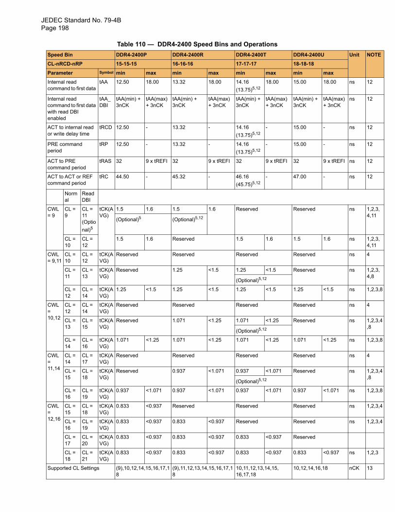
JEDEC Standard No. 79-4BPage 198
it NOTE
12
12
12
12
12
12
1,2,3, 4,11
1,2,3, 4,11
4
1,2,3, 4,8
1,2,3,8
4
1,2,3,4,8
1,2,3,8
4
1,2,3,4,8
1,2,3,8
1,2,3,4
1,2,3,4
1,2,3
K 13
Table 110 — DDR4-2400 Speed Bins and Operations
Speed Bin DDR4-2400P DDR4-2400R DDR4-2400T DDR4-2400U Un
CL-nRCD-nRP 15-15-15 16-16-16 17-17-17 18-18-18
Parameter Symbol min max min max min max min max
Internal read command to first data
tAA 12.50 18.00 13.32 18.00 14.16
(13.75)5,12
18.00 15.00 18.00 ns
Internal read command to first data with read DBI enabled
tAA_DBI
tAA(min) + 3nCK
tAA(max) + 3nCK
tAA(min) + 3nCK
tAA(max) + 3nCK
tAA(min) + 3nCK
tAA(max) + 3nCK
tAA(min) + 3nCK
tAA(max) + 3nCK
ns
ACT to internal read or write delay time
tRCD 12.50 - 13.32 - 14.16
(13.75)5,12
- 15.00 - ns
PRE command period
tRP 12.50 - 13.32 - 14.16
(13.75)5,12
- 15.00 - ns
ACT to PRE command period
tRAS 32 9 x tREFI 32 9 x tREFI 32 9 x tREFI 32 9 x tREFI ns
ACT to ACT or REF command period
tRC 44.50 - 45.32 - 46.16
(45.75)5,12
- 47.00 - ns
Normal
Read DBI
CWL = 9
CL = 9
CL = 11(Optio
nal)5
tCK(AVG)
1.5 1.6 1.5 1.6 Reserved Reserved ns
(Optional)5 (Optional)5,12
CL = 10
CL = 12
1.5 1.6 Reserved 1.5 1.6 1.5 1.6 ns
CWL = 9,11
CL = 10
CL = 12
tCK(AVG)
Reserved Reserved Reserved Reserved ns
CL = 11
CL = 13
tCK(AVG)
Reserved 1.25 <1.5 1.25 <1.5 Reserved ns
(Optional)5,12
CL = 12
CL = 14
tCK(AVG)
1.25 <1.5 1.25 <1.5 1.25 <1.5 1.25 <1.5 ns
CWL = 10,12
CL = 12
CL = 14
tCK(AVG)
Reserved Reserved Reserved Reserved ns
CL = 13
CL = 15
tCK(AVG)
Reserved 1.071 <1.25 1.071 <1.25 Reserved ns
(Optional)5,12
CL = 14
CL = 16
tCK(AVG)
1.071 <1.25 1.071 <1.25 1.071 <1.25 1.071 <1.25 ns
CWL = 11,14
CL = 14
CL = 17
tCK(AVG)
Reserved Reserved Reserved Reserved ns
CL = 15
CL = 18
tCK(AVG)
Reserved 0.937 <1.071 0.937 <1.071 Reserved ns
(Optional)5,12
CL = 16
CL = 19
tCK(AVG)
0.937 <1.071 0.937 <1.071 0.937 <1.071 0.937 <1.071 ns
CWL = 12,16
CL = 15
CL = 18
tCK(AVG)
0.833 <0.937 Reserved Reserved Reserved ns
CL = 16
CL = 19
tCK(AVG)
0.833 <0.937 0.833 <0.937 Reserved Reserved ns
CL = 17
CL = 20
tCK(AVG)
0.833 <0.937 0.833 <0.937 0.833 <0.937 Reserved
CL = 18
CL = 21
tCK(AVG)
0.833 <0.937 0.833 <0.937 0.833 <0.937 0.833 <0.937 ns
Supported CL Settings (9),10,12,14,15,16,17,18
(9),11,12,13,14,15,16,17,18
10,11,12,13,14,15,16,17,18
10,12,14,16,18 nC
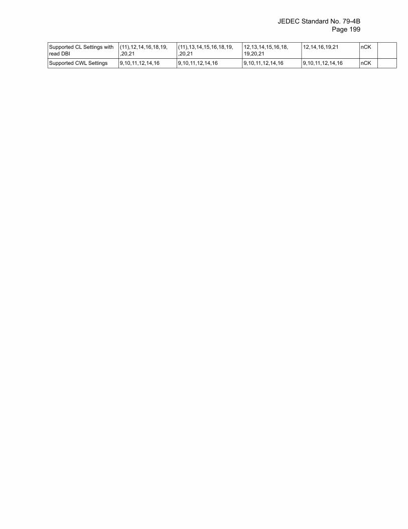
JEDEC Standard No. 79-4B Page 199
K
K
Supported CL Settings with read DBI
(11),12,14,16,18,19, ,20,21
(11),13,14,15,16,18,19, ,20,21
12,13,14,15,16,18,19,20,21
12,14,16,19,21 nC
Supported CWL Settings 9,10,11,12,14,16 9,10,11,12,14,16 9,10,11,12,14,16 9,10,11,12,14,16 nC
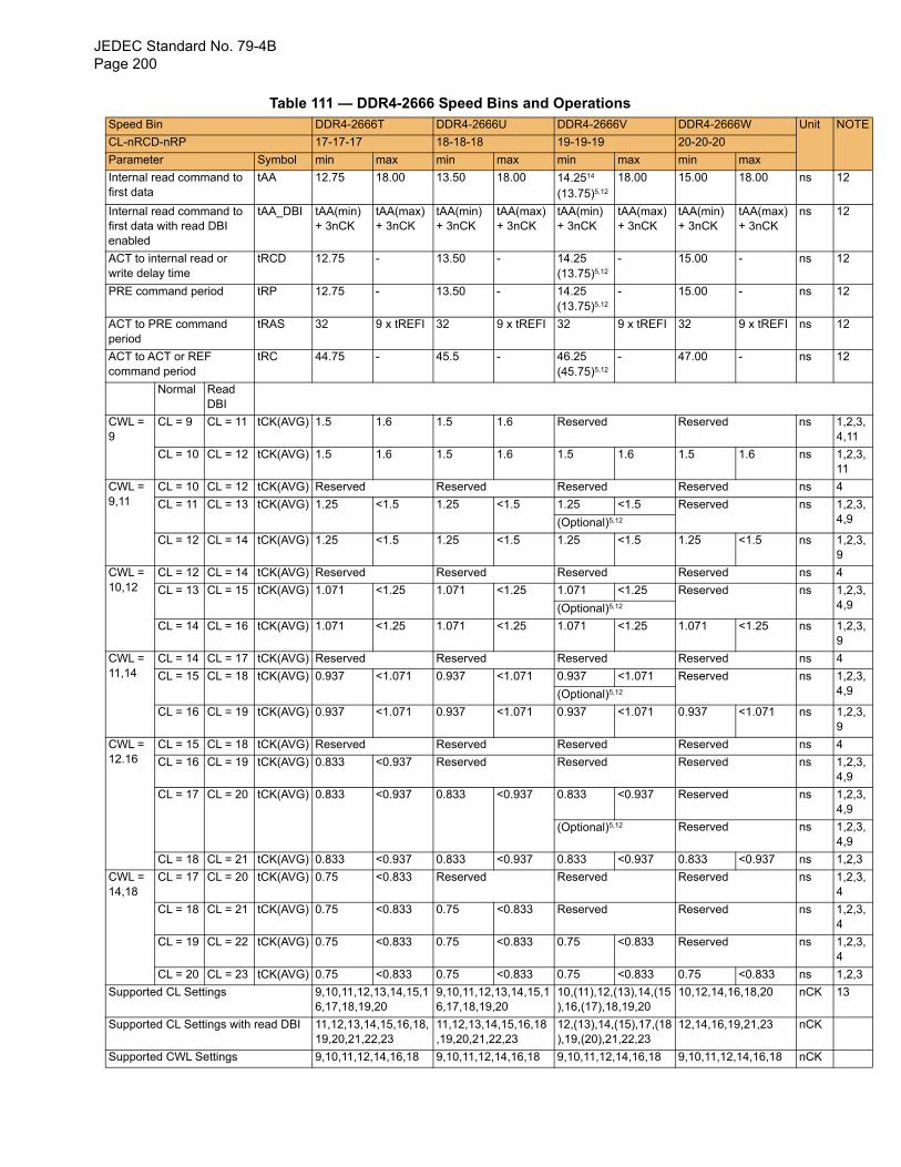
JEDEC Standard No. 79-4BPage 200
it NOTE
12
12
12
12
12
12
1,2,3,4,11
1,2,3,11
4
1,2,3,4,9
1,2,3,9
4
1,2,3,4,9
1,2,3,9
4
1,2,3,4,9
1,2,3,9
4
1,2,3,4,9
1,2,3,4,9
1,2,3,4,9
1,2,3
1,2,3,4
1,2,3,4
1,2,3,4
1,2,3
K 13
K
K
Table 111 — DDR4-2666 Speed Bins and OperationsSpeed Bin DDR4-2666T DDR4-2666U DDR4-2666V DDR4-2666W Un
CL-nRCD-nRP 17-17-17 18-18-18 19-19-19 20-20-20
Parameter Symbol min max min max min max min max
Internal read command to first data
tAA 12.75 18.00 13.50 18.00 14.2514
(13.75)5,12
18.00 15.00 18.00 ns
Internal read command to first data with read DBI enabled
tAA_DBI tAA(min) + 3nCK
tAA(max) + 3nCK
tAA(min) + 3nCK
tAA(max) + 3nCK
tAA(min) + 3nCK
tAA(max) + 3nCK
tAA(min) + 3nCK
tAA(max) + 3nCK
ns
ACT to internal read or write delay time
tRCD 12.75 - 13.50 - 14.25(13.75)5,12
- 15.00 - ns
PRE command period tRP 12.75 - 13.50 - 14.25(13.75)5,12
- 15.00 - ns
ACT to PRE command period
tRAS 32 9 x tREFI 32 9 x tREFI 32 9 x tREFI 32 9 x tREFI ns
ACT to ACT or REF command period
tRC 44.75 - 45.5 - 46.25(45.75)5,12
- 47.00 - ns
Normal Read DBI
CWL = 9
CL = 9 CL = 11 tCK(AVG) 1.5 1.6 1.5 1.6 Reserved Reserved ns
CL = 10 CL = 12 tCK(AVG) 1.5 1.6 1.5 1.6 1.5 1.6 1.5 1.6 ns
CWL = 9,11
CL = 10 CL = 12 tCK(AVG) Reserved Reserved Reserved Reserved ns
CL = 11 CL = 13 tCK(AVG) 1.25 <1.5 1.25 <1.5 1.25 <1.5 Reserved ns
(Optional)5,12
CL = 12 CL = 14 tCK(AVG) 1.25 <1.5 1.25 <1.5 1.25 <1.5 1.25 <1.5 ns
CWL = 10,12
CL = 12 CL = 14 tCK(AVG) Reserved Reserved Reserved Reserved ns
CL = 13 CL = 15 tCK(AVG) 1.071 <1.25 1.071 <1.25 1.071 <1.25 Reserved ns
(Optional)5,12
CL = 14 CL = 16 tCK(AVG) 1.071 <1.25 1.071 <1.25 1.071 <1.25 1.071 <1.25 ns
CWL = 11,14
CL = 14 CL = 17 tCK(AVG) Reserved Reserved Reserved Reserved ns
CL = 15 CL = 18 tCK(AVG) 0.937 <1.071 0.937 <1.071 0.937 <1.071 Reserved ns
(Optional)5,12
CL = 16 CL = 19 tCK(AVG) 0.937 <1.071 0.937 <1.071 0.937 <1.071 0.937 <1.071 ns
CWL = 12.16
CL = 15 CL = 18 tCK(AVG) Reserved Reserved Reserved Reserved ns
CL = 16 CL = 19 tCK(AVG) 0.833 <0.937 Reserved Reserved Reserved ns
CL = 17 CL = 20 tCK(AVG) 0.833 <0.937 0.833 <0.937 0.833 <0.937 Reserved ns
(Optional)5,12 Reserved ns
CL = 18 CL = 21 tCK(AVG) 0.833 <0.937 0.833 <0.937 0.833 <0.937 0.833 <0.937 ns
CWL = 14,18
CL = 17 CL = 20 tCK(AVG) 0.75 <0.833 Reserved Reserved Reserved ns
CL = 18 CL = 21 tCK(AVG) 0.75 <0.833 0.75 <0.833 Reserved Reserved ns
CL = 19 CL = 22 tCK(AVG) 0.75 <0.833 0.75 <0.833 0.75 <0.833 Reserved ns
CL = 20 CL = 23 tCK(AVG) 0.75 <0.833 0.75 <0.833 0.75 <0.833 0.75 <0.833 ns
Supported CL Settings 9,10,11,12,13,14,15,16,17,18,19,20
9,10,11,12,13,14,15,16,17,18,19,20
10,(11),12,(13),14,(15),16,(17),18,19,20
10,12,14,16,18,20 nC
Supported CL Settings with read DBI 11,12,13,14,15,16,18,19,20,21,22,23
11,12,13,14,15,16,18,19,20,21,22,23
12,(13),14,(15),17,(18),19,(20),21,22,23
12,14,16,19,21,23 nC
Supported CWL Settings 9,10,11,12,14,16,18 9,10,11,12,14,16,18 9,10,11,12,14,16,18 9,10,11,12,14,16,18 nC
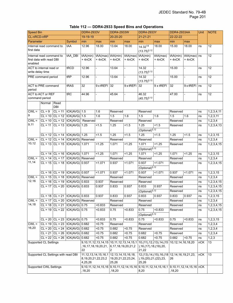
JEDEC Standard No. 79-4B Page 201
OTE
2
2
2
2
2
2
,2,3,4,11
,2,3,11
,2,3,4
,2,3,4,13
,2,3,15
,2,3,4
,2,3,4,15
,2,3,15
,2,3,4
,2,3,4,15
,2,3,15
,2,3,4
,2,3,4,15
,2,3,4,15
,2,3,4,15
,2,3,15
,2,3,4
,2,3,4,15
,2,3,4,15
,2,3,15
,2,3,4
,2,3,4
,2,3,4
,2,3
3
3
Table 112 — DDR4-2933 Speed Bins and OperationsSpeed Bin DDR4-2933V DDR4-2933W DDR4-2933Y DDR4-2933AA Unit N
CL-nRCD-nRP 19-19-19 20-20-20 21-21-21 22-22-22
Parameter Symbol min max min max min max min max
Internal read command to first data
tAA 12.96 18.00 13.64 18.00 14.3214
(13.75)5,12
18.00 15.00 18.00 ns 1
Internal read command to first data with read DBI enabled
tAA_DBI tAA(min) + 4nCK
tAA(max) + 4nCK
tAA(min) + 4nCK
tAA(max) + 4nCK
tAA(min) + 4nCK
tAA(max) + 4nCK
tAA(min) + 4nCK
tAA(max) + 4nCK
ns 1
ACT to internal read or write delay time
tRCD 12.96 - 13.64 - 14.32
(13.75)5,12
- 15.00 - ns 1
PRE command period tRP 12.96 - 13.64 - 14.32
(13.75)5,12
- 15.00 - ns 1
ACT to PRE command period
tRAS 32 9 x tREFI 32 9 x tREFI 32 9 x tREFI 32 9 x tREFI ns 1
ACT to ACT or REF command period
tRC 44.96 - 45.64 - 46.32
(45.75)5,12
- 47.00 - ns 1
Normal Read DBI
CWL = 9
CL = 9 CL = 11 tCK(AVG) 1.5 1.6 Reserved Reserved Reserved ns 1
CL = 10 CL = 12 tCK(AVG) 1.5 1.6 1.5 1.6 1.5 1.6 1.5 1.6 ns 1
CWL = 9,11
CL = 10 CL = 12 tCK(AVG) Reserved Reserved Reserved Reserved ns 1
CL = 11 CL = 13 tCK(AVG) 1.25 <1.5 1.25 <1.5 1.25 <1.5 Reserved ns 1
(Optional)5,12
CL = 12 CL = 14 tCK(AVG) 1.25 <1.5 1.25 <1.5 1.25 <1.5 1.25 <1.5 ns 1
CWL = 10,12
CL = 12 CL = 14 tCK(AVG) Reserved Reserved Reserved Reserved ns 1
CL = 13 CL = 15 tCK(AVG) 1.071 <1.25 1.071 <1.25 1.071 <1.25 Reserved ns 1
(Optional)5,12
CL = 14 CL = 16 tCK(AVG) 1.071 <1.25 1.071 <1.25 1.071 <1.25 1.071 <1.25 ns 1
CWL = 11,14
CL = 14 CL = 17 tCK(AVG) Reserved Reserved Reserved Reserved ns 1
CL = 15 CL = 18 tCK(AVG) 0.937 <1.071 0.937 <1.071 0.937 <1.071 Reserved ns 1
(Optional)5,12
CL = 16 CL = 19 tCK(AVG) 0.937 <1.071 0.937 <1.071 0.937 <1.071 0.937 <1.071 ns 1
CWL = 12.16
CL = 15 CL = 18 tCK(AVG) Reserved Reserved Reserved Reserved ns 1
CL = 16 CL = 19 tCK(AVG) 0.833 0.937 Reserved Reserved Reserved ns 1
CL = 17 CL = 20 tCK(AVG) 0.833 0.937 0.833 0.937 0.833 0.937 Reserved ns 1
(Optional)5,12 Reserved ns 1
CL = 18 CL = 21 tCK(AVG) 0.833 0.937 0.833 0.937 0.833 0.937 0.833 0.937 ns 1
CWL = 14,18
CL = 17 CL = 20 tCK(AVG) Reserved Reserved Reserved Reserved ns 1
CL = 18 CL = 21 tCK(AVG) 0.75 <0.833 Reserved Reserved Reserved ns 1
CL = 19 CL = 22 tCK(AVG) 0.75 <0.833 0.75 <0.833 0.75 <0.833 Reserved ns 1
(Optional)5,12
CL = 20 CL = 23 tCK(AVG) 0.75 <0.833 0.75 <0.833 0.75 <0.833 0.75 <0.833 ns 1
CWL = 16,20
CL = 19 CL = 23 tCK(AVG) 0.682 <0.75 Reserved Reserved Reserved ns 1
CL = 20 CL = 24 tCK(AVG) 0.682 <0.75 0.682 <0.75 Reserved Reserved ns 1
CL = 21 CL = 26 tCK(AVG) 0.682 <0.75 0.682 <0.75 0.682 <0.75 Reserved ns 1
CL = 22 CL = 26 tCK(AVG) 0.682 <0.75 0.682 <0.75 0.682 <0.75 0.682 <0.75 ns 1
Supported CL Settings 9,10,11,12,13,14,15,16,17,18,19,20,21,22
10,11,12,13,14,15,16,17,18,19,20,21,22
10,(11),12,(13),14,(15),16,(17),18,(19),20,21,22
10,12,14,16,18,20 nCK 1
Supported CL Settings with read DBI 11,12,13,14,15,16,18,19,20,21,22,23,24,25,26
12,13,14,15,16,18,19,20,21,22,23,24,25,26
12,(13),14,(15),16,(18),19,(20),21,(22),23,25,26
12,14,16,19,21,23,26
nCK 1
Supported CWL Settings 9,10,11,12,14,15,16,18,20
9,10,11,12,14,15,16,18,20
9,10,11,12,14,15,16,18,20
9,10,11,12,14,15,16,18,20
nCK
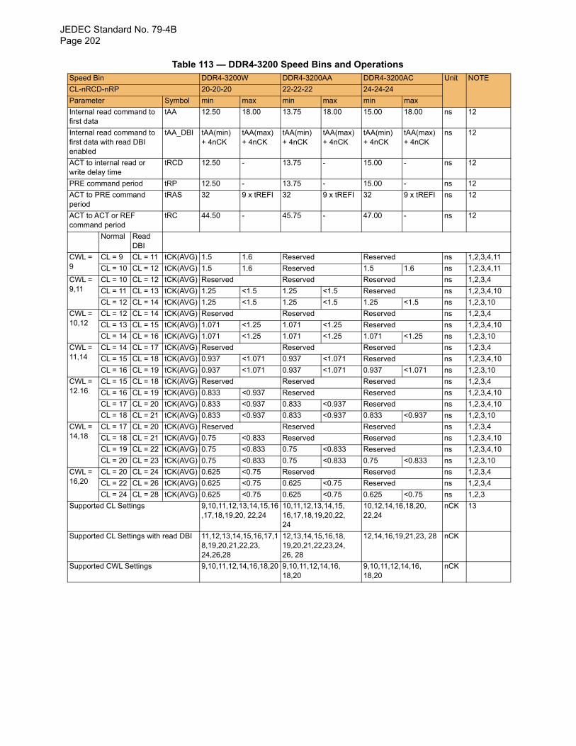
JEDEC Standard No. 79-4BPage 202
Table 113 — DDR4-3200 Speed Bins and OperationsSpeed Bin DDR4-3200W DDR4-3200AA DDR4-3200AC Unit NOTE
CL-nRCD-nRP 20-20-20 22-22-22 24-24-24
Parameter Symbol min max min max min max
Internal read command to first data
tAA 12.50 18.00 13.75 18.00 15.00 18.00 ns 12
Internal read command to first data with read DBI enabled
tAA_DBI tAA(min) + 4nCK
tAA(max) + 4nCK
tAA(min) + 4nCK
tAA(max) + 4nCK
tAA(min) + 4nCK
tAA(max) + 4nCK
ns 12
ACT to internal read or write delay time
tRCD 12.50 - 13.75 - 15.00 - ns 12
PRE command period tRP 12.50 - 13.75 - 15.00 - ns 12
ACT to PRE command period
tRAS 32 9 x tREFI 32 9 x tREFI 32 9 x tREFI ns 12
ACT to ACT or REF command period
tRC 44.50 - 45.75 - 47.00 - ns 12
Normal Read DBI
CWL = 9
CL = 9 CL = 11 tCK(AVG) 1.5 1.6 Reserved Reserved ns 1,2,3,4,11
CL = 10 CL = 12 tCK(AVG) 1.5 1.6 Reserved 1.5 1.6 ns 1,2,3,4,11
CWL = 9,11
CL = 10 CL = 12 tCK(AVG) Reserved Reserved Reserved ns 1,2,3,4
CL = 11 CL = 13 tCK(AVG) 1.25 <1.5 1.25 <1.5 Reserved ns 1,2,3,4,10
CL = 12 CL = 14 tCK(AVG) 1.25 <1.5 1.25 <1.5 1.25 <1.5 ns 1,2,3,10
CWL = 10,12
CL = 12 CL = 14 tCK(AVG) Reserved Reserved Reserved ns 1,2,3,4
CL = 13 CL = 15 tCK(AVG) 1.071 <1.25 1.071 <1.25 Reserved ns 1,2,3,4,10
CL = 14 CL = 16 tCK(AVG) 1.071 <1.25 1.071 <1.25 1.071 <1.25 ns 1,2,3,10
CWL = 11,14
CL = 14 CL = 17 tCK(AVG) Reserved Reserved Reserved ns 1,2,3,4
CL = 15 CL = 18 tCK(AVG) 0.937 <1.071 0.937 <1.071 Reserved ns 1,2,3,4,10
CL = 16 CL = 19 tCK(AVG) 0.937 <1.071 0.937 <1.071 0.937 <1.071 ns 1,2,3,10
CWL = 12.16
CL = 15 CL = 18 tCK(AVG) Reserved Reserved Reserved ns 1,2,3,4
CL = 16 CL = 19 tCK(AVG) 0.833 <0.937 Reserved Reserved ns 1,2,3,4,10
CL = 17 CL = 20 tCK(AVG) 0.833 <0.937 0.833 <0.937 Reserved ns 1,2,3,4,10
CL = 18 CL = 21 tCK(AVG) 0.833 <0.937 0.833 <0.937 0.833 <0.937 ns 1,2,3,10
CWL = 14,18
CL = 17 CL = 20 tCK(AVG) Reserved Reserved Reserved ns 1,2,3,4
CL = 18 CL = 21 tCK(AVG) 0.75 <0.833 Reserved Reserved ns 1,2,3,4,10
CL = 19 CL = 22 tCK(AVG) 0.75 <0.833 0.75 <0.833 Reserved ns 1,2,3,4,10
CL = 20 CL = 23 tCK(AVG) 0.75 <0.833 0.75 <0.833 0.75 <0.833 ns 1,2,3,10
CWL = 16,20
CL = 20 CL = 24 tCK(AVG) 0.625 <0.75 Reserved Reserved ns 1,2,3,4
CL = 22 CL = 26 tCK(AVG) 0.625 <0.75 0.625 <0.75 Reserved ns 1,2,3,4
CL = 24 CL = 28 tCK(AVG) 0.625 <0.75 0.625 <0.75 0.625 <0.75 ns 1,2,3
Supported CL Settings 9,10,11,12,13,14,15,16,17,18,19,20, 22,24
10,11,12,13,14,15, 16,17,18,19,20,22,24
10,12,14,16,18,20,22,24
nCK 13
Supported CL Settings with read DBI 11,12,13,14,15,16,17,18,19,20,21,22,23,24,26,28
12,13,14,15,16,18, 19,20,21,22,23,24,26, 28
12,14,16,19,21,23, 28 nCK
Supported CWL Settings 9,10,11,12,14,16,18,20 9,10,11,12,14,16,18,20
9,10,11,12,14,16,18,20
nCK
JEDEC Standard No. 79-4B Page 203
10.1 Speed Bin Table NoteAbsolute Specification - VDDQ = VDD = 1.20V +/- 0.06 V - VPP = 2.5V +0.25/-0.125 V - The values defined with above-mentioned table are DLL ON case.
- DDR4-1600, 1866, 2133 and 2400 Speed Bin Tables are valid only when Geardown Mode is disabled.
1. The CL setting and CWL setting result in tCK(avg).MIN and tCK(avg).MAX requirements. When making a selection of tCK(avg), both need to be fulfilled: Requirements from CL setting as well as requirements from CWL setting.
2. tCK(avg).MIN limits: Since CAS Latency is not purely analog - data and strobe output are synchronized by the DLL - all possible intermediate frequencies may not be guaranteed. CL in clock cycle is calculated from tAA following rounding algorithm defined in Section 13.5.
3. tCK(avg).MAX limits: Calculate tCK(avg) = tAA.MAX / CL SELECTED and round the resulting tCK(avg) down to the next valid speed bin (i.e. 1.5ns or 1.25ns or 1.071 ns or 0.937 ns or 0.833 ns). This result is tCK(avg).MAX corresponding to CL SELECTED.
4. ‘Reserved’ settings are not allowed. User must program a different value.5. 'Optional' settings allow certain devices in the industry to support this setting, however, it is not a mandatory feature. Refer to supplier's data sheet
and/or the DIMM SPD information if and how this setting is supported.6. Any DDR4-1866 speed bin also supports functional operation at lower frequencies as shown in the table which are not subject to Production Tests but
verified by Design/Characterization.7. Any DDR4-2133 speed bin also supports functional operation at lower frequencies as shown in the table which are not subject to Production Tests but
verified by Design/Characterization.8. Any DDR4-2400 speed bin also supports functional operation at lower frequencies as shown in the table which are not subject to Production Tests but
verified by Design/Characterization.9. Any DDR4-2666 speed bin also supports functional operation at lower frequencies as shown in the table which are not subject to Production Tests but
verified by Design/Characterization.10. Any DDR4-3200 speed bin also supports functional operation at lower frequencies as shown in the table which are not subject to Production Tests
but verified by Design/Characterization.11. DDR4-1600 AC timing apply if DRAM operates at lower than 1600 MT/s data rate.12. Parameters apply from tCK(avg)min to tCK(avg)max at all standard JEDEC clock period values as stated in the Speed Bin Tables.13. CL number in parentheses, it means that these numbers are optional.14. DDR4 SDRAM supports CL=9 as long as a system meets tAA(min).
16. Each speed bin lists the timing requirements that need to be supported in order for a given DRAM to be JEDEC compliant. JEDEC compliance does not require support for all speed bins within a given speed. JEDEC compliance requires meeting the parameters for a least one of the listed speed bins.
JEDEC Standard No. 79-4BPage 204
11 IDD and IDDQ Specification Parameters and Test conditions
11.1 IDD, IPP and IDDQ Measurement ConditionsIn this chapter, IDD, IPP and IDDQ measurement conditions such as test load and patterns are defined. Figure 208 shows the setup and test load for IDD, IPP and IDDQ measurements.
IDD currents (such as IDD0, IDD0A, IDD1, IDD1A, IDD2N, IDD2NA, IDD2NL, IDD2NT, IDD2P, IDD2Q, IDD3N, IDD3NA, IDD3P, IDD4R, IDD4RA, IDD4W, IDD4WA, IDD5B, IDD5F2, IDD5F4, IDD6N, IDD6E, IDD6R, IDD6A, IDD7 and IDD8) are measured as time-averaged currents with all VDD balls of the DDR4 SDRAM under test tied together. Any IPP or IDDQ current is not included in IDD currents.
IPP currents have the same definition as IDD except that the current on the VPP supply is measured.
IDDQ currents (such as IDDQ2NT and IDDQ4R) are measured as time-averaged currents with all VDDQ balls of the DDR4 SDRAM under test tied together. Any IDD current is not included in IDDQ currents.Attention: IDDQ values cannot be directly used to calculate IO power of the DDR4 SDRAM. They can be used to support correlation of simulated IO power to actual IO power as outlined in Figure 209. In DRAM module application, IDDQ cannot be measured separately since VDD and VDDQ are using one merged-power layer in Module PCB.
For IDD, IPP and IDDQ measurements, the following definitions apply:
“0” and “LOW” is defined as VIN <= VILAC(max).
“1” and “HIGH” is defined as VIN >= VIHAC(min).
“MID-LEVEL” is defined as inputs are VREF = VDD / 2.
Timings used for IDD, IPP and IDDQ Measurement-Loop Patterns are provided in Table 114.
Basic IDD, IPP and IDDQ Measurement Conditions are described in Table 115.
Detailed IDD, IPP and IDDQ Measurement-Loop Patterns are described in Table 116 through Table 124.
IDD Measurements are done after properly initializing the DDR4 SDRAM. This includes but is not limited to setting RON = RZQ/7 (34 Ohm in MR1); RTT_NOM = RZQ/6 (40 Ohm in MR1);RTT_WR = RZQ/2 (120 Ohm in MR2);RTT_PARK = Disable;Qoff = 0B (Output Buffer enabled) in MR1;TDQS_t disabled in MR1;CRC disabled in MR2;CA parity feature disabled in MR5;
Gear down mode disabled in MR3 Read/Write DBI disabled in MR5; DM disabled in MR5
Attention: The IDD, IPP and IDDQ Measurement-Loop Patterns need to be executed at least one time before actual IDD or IDDQ measurement is started.
Define D = {CS_n, ACT_n, RAS_n, CAS_n, WE_n }:= {HIGH, LOW, LOW, LOW, LOW}; apply BG/BA changes when directed.
Define D# = {CS_n, ACT_n, RAS_n, CAS_n, WE_n }:= {HIGH, HIGH, HIGH, HIGH, HIGH}; apply invert of BG/BA changes when directed above.
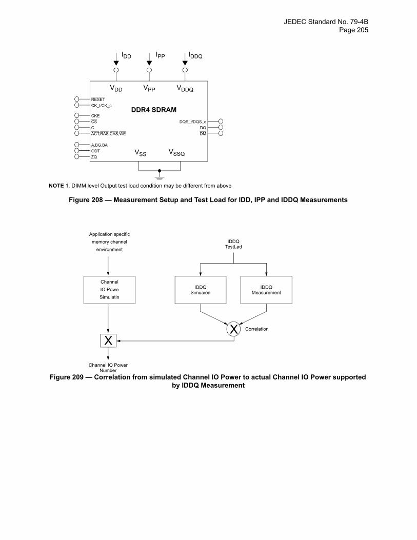
JEDEC Standard No. 79-4B Page 205
NOTE 1. DIMM level Output test load condition may be different from above
Figure 208 — Measurement Setup and Test Load for IDD, IPP and IDDQ Measurements
Figure 209 — Correlation from simulated Channel IO Power to actual Channel IO Power supported by IDDQ Measurement
RESET
CK_t/CK_c
CKE
CS
ACT,RAS,CAS,WE
A,BG,BA
C
ODT
ZQ
DQS_t/DQS_c
DQ
DM
DDR4 SDRAM
VSS VSSQ
VDD VPP VDDQ
IDD IPP IDDQ
X
Application specific
memory channel
environment
Channel
IO Powe
Simulatin
X
Channel IO PowerNumber
IDDQTestLad
IDDQSimuaion
IDDQMeasurement
Correlation
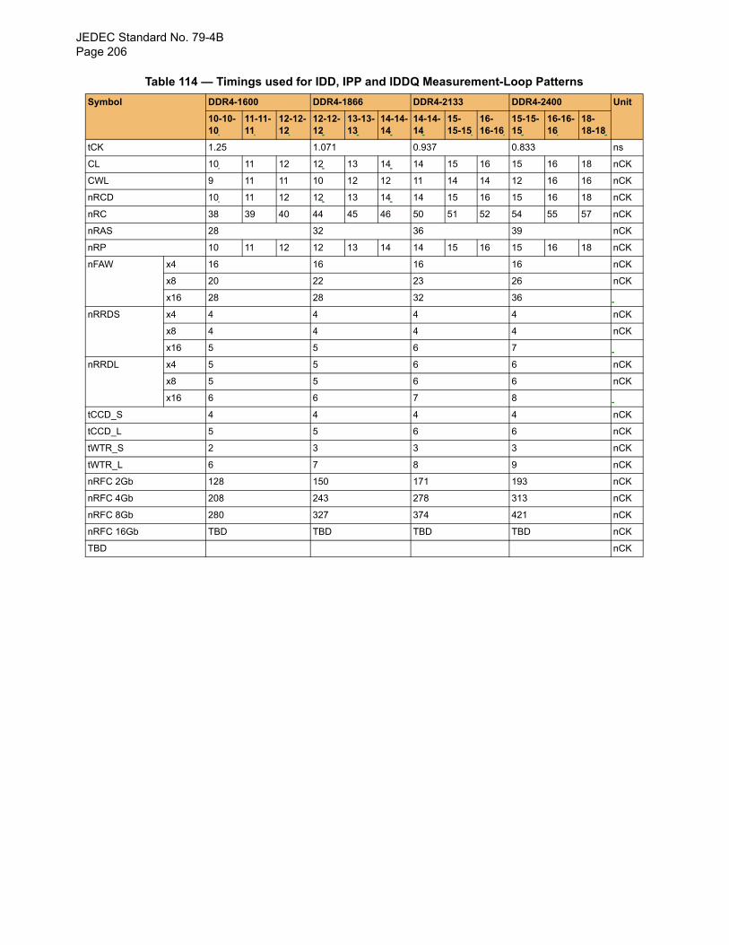
JEDEC Standard No. 79-4BPage 206
Table 114 — Timings used for IDD, IPP and IDDQ Measurement-Loop Patterns
Symbol DDR4-1600 DDR4-1866 DDR4-2133 DDR4-2400 Unit
10-10-10
11-11-11
12-12-12
12-12-12
13-13-13
14-14-14
14-14-14
15-15-15
16-16-16
15-15-15
16-16-16
18-18-18
tCK 1.25 1.071 0.937 0.833 ns
CL 10 11 12 12 13 14 14 15 16 15 16 18 nCK
CWL 9 11 11 10 12 12 11 14 14 12 16 16 nCK
nRCD 10 11 12 12 13 14 14 15 16 15 16 18 nCK
nRC 38 39 40 44 45 46 50 51 52 54 55 57 nCK
nRAS 28 32 36 39 nCK
nRP 10 11 12 12 13 14 14 15 16 15 16 18 nCK
nFAW x4 16 16 16 16 nCK
x8 20 22 23 26 nCK
x16 28 28 32 36
nRRDS x4 4 4 4 4 nCK
x8 4 4 4 4 nCK
x16 5 5 6 7
nRRDL x4 5 5 6 6 nCK
x8 5 5 6 6 nCK
x16 6 6 7 8
tCCD_S 4 4 4 4 nCK
tCCD_L 5 5 6 6 nCK
tWTR_S 2 3 3 3 nCK
tWTR_L 6 7 8 9 nCK
nRFC 2Gb 128 150 171 193 nCK
nRFC 4Gb 208 243 278 313 nCK
nRFC 8Gb 280 327 374 421 nCK
nRFC 16Gb TBD TBD TBD TBD nCK
TBD nCK
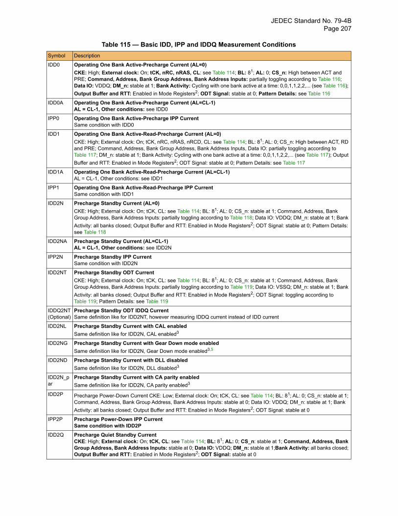
JEDEC Standard No. 79-4B Page 207
Table 115 — Basic IDD, IPP and IDDQ Measurement Conditions
Symbol Description
IDD0 Operating One Bank Active-Precharge Current (AL=0)
CKE: High; External clock: On; tCK, nRC, nRAS, CL: see Table 114; BL: 81; AL: 0; CS_n: High between ACT and PRE; Command, Address, Bank Group Address, Bank Address Inputs: partially toggling according to Table 116; Data IO: VDDQ; DM_n: stable at 1; Bank Activity: Cycling with one bank active at a time: 0,0,1,1,2,2,... (see Table 116);
Output Buffer and RTT: Enabled in Mode Registers2; ODT Signal: stable at 0; Pattern Details: see Table 116
IDD0A Operating One Bank Active-Precharge Current (AL=CL-1)AL = CL-1, Other conditions: see IDD0
IPP0 Operating One Bank Active-Precharge IPP CurrentSame condition with IDD0
IDD1 Operating One Bank Active-Read-Precharge Current (AL=0)
CKE: High; External clock: On; tCK, nRC, nRAS, nRCD, CL: see Table 114; BL: 81; AL: 0; CS_n: High between ACT, RD and PRE; Command, Address, Bank Group Address, Bank Address Inputs, Data IO: partially toggling according to Table 117; DM_n: stable at 1; Bank Activity: Cycling with one bank active at a time: 0,0,1,1,2,2,... (see Table 117); Output
Buffer and RTT: Enabled in Mode Registers2; ODT Signal: stable at 0; Pattern Details: see Table 117
IDD1A Operating One Bank Active-Read-Precharge Current (AL=CL-1)AL = CL-1, Other conditions: see IDD1
IPP1 Operating One Bank Active-Read-Precharge IPP CurrentSame condition with IDD1
IDD2N Precharge Standby Current (AL=0)
CKE: High; External clock: On; tCK, CL: see Table 114; BL: 81; AL: 0; CS_n: stable at 1; Command, Address, Bank Group Address, Bank Address Inputs: partially toggling according to Table 118; Data IO: VDDQ; DM_n: stable at 1; Bank
Activity: all banks closed; Output Buffer and RTT: Enabled in Mode Registers2; ODT Signal: stable at 0; Pattern Details: see Table 118
IDD2NA Precharge Standby Current (AL=CL-1)AL = CL-1, Other conditions: see IDD2N
IPP2N Precharge Standby IPP CurrentSame condition with IDD2N
IDD2NT Precharge Standby ODT Current
CKE: High; External clock: On; tCK, CL: see Table 114; BL: 81; AL: 0; CS_n: stable at 1; Command, Address, Bank Group Address, Bank Address Inputs: partially toggling according to Table 119; Data IO: VSSQ; DM_n: stable at 1; Bank
Activity: all banks closed; Output Buffer and RTT: Enabled in Mode Registers2; ODT Signal: toggling according to Table 119; Pattern Details: see Table 119
IDDQ2NT(Optional)
Precharge Standby ODT IDDQ CurrentSame definition like for IDD2NT, however measuring IDDQ current instead of IDD current
IDD2NL Precharge Standby Current with CAL enabled
Same definition like for IDD2N, CAL enabled3
IDD2NG Precharge Standby Current with Gear Down mode enabled
Same definition like for IDD2N, Gear Down mode enabled3,5
IDD2ND Precharge Standby Current with DLL disabled
Same definition like for IDD2N, DLL disabled3
IDD2N_par
Precharge Standby Current with CA parity enabled
Same definition like for IDD2N, CA parity enabled3
IDD2P Precharge Power-Down Current CKE: Low; External clock: On; tCK, CL: see Table 114; BL: 81; AL: 0; CS_n: stable at 1; Command, Address, Bank Group Address, Bank Address Inputs: stable at 0; Data IO: VDDQ; DM_n: stable at 1; Bank
Activity: all banks closed; Output Buffer and RTT: Enabled in Mode Registers2; ODT Signal: stable at 0
IPP2P Precharge Power-Down IPP Current Same condition with IDD2P
IDD2Q Precharge Quiet Standby CurrentCKE: High; External clock: On; tCK, CL: see Table 114; BL: 81; AL: 0; CS_n: stable at 1; Command, Address, Bank Group Address, Bank Address Inputs: stable at 0; Data IO: VDDQ; DM_n: stable at 1;Bank Activity: all banks closed; Output Buffer and RTT: Enabled in Mode Registers2; ODT Signal: stable at 0
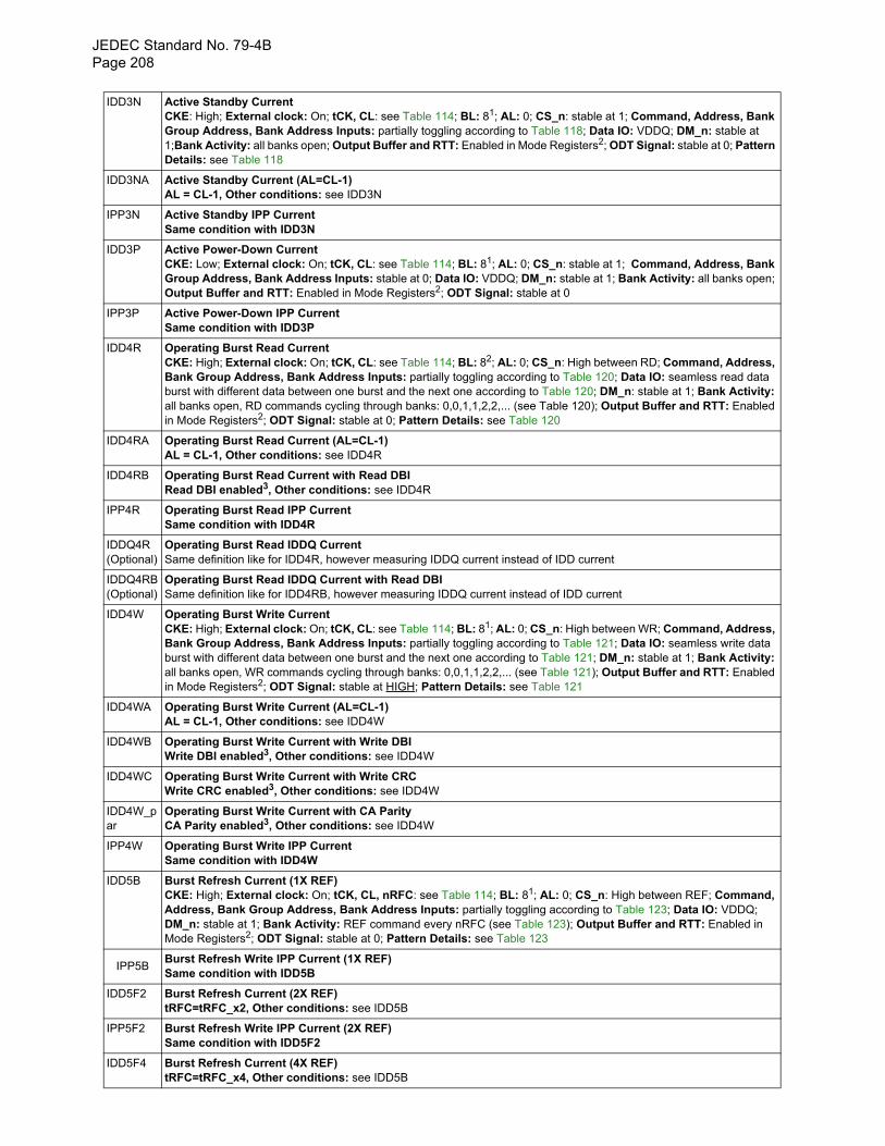
JEDEC Standard No. 79-4BPage 208
IDD3N Active Standby CurrentCKE: High; External clock: On; tCK, CL: see Table 114; BL: 81; AL: 0; CS_n: stable at 1; Command, Address, Bank Group Address, Bank Address Inputs: partially toggling according to Table 118; Data IO: VDDQ; DM_n: stable at 1;Bank Activity: all banks open; Output Buffer and RTT: Enabled in Mode Registers2; ODT Signal: stable at 0; Pattern Details: see Table 118
IDD3NA Active Standby Current (AL=CL-1)AL = CL-1, Other conditions: see IDD3N
IPP3N Active Standby IPP Current Same condition with IDD3N
IDD3P Active Power-Down CurrentCKE: Low; External clock: On; tCK, CL: see Table 114; BL: 81; AL: 0; CS_n: stable at 1; Command, Address, Bank Group Address, Bank Address Inputs: stable at 0; Data IO: VDDQ; DM_n: stable at 1; Bank Activity: all banks open; Output Buffer and RTT: Enabled in Mode Registers2; ODT Signal: stable at 0
IPP3P Active Power-Down IPP Current Same condition with IDD3P
IDD4R Operating Burst Read CurrentCKE: High; External clock: On; tCK, CL: see Table 114; BL: 82; AL: 0; CS_n: High between RD; Command, Address, Bank Group Address, Bank Address Inputs: partially toggling according to Table 120; Data IO: seamless read data burst with different data between one burst and the next one according to Table 120; DM_n: stable at 1; Bank Activity: all banks open, RD commands cycling through banks: 0,0,1,1,2,2,... (see Table 120); Output Buffer and RTT: Enabled in Mode Registers2; ODT Signal: stable at 0; Pattern Details: see Table 120
IDD4RA Operating Burst Read Current (AL=CL-1)AL = CL-1, Other conditions: see IDD4R
IDD4RB Operating Burst Read Current with Read DBIRead DBI enabled3, Other conditions: see IDD4R
IPP4R Operating Burst Read IPP Current Same condition with IDD4R
IDDQ4R(Optional)
Operating Burst Read IDDQ CurrentSame definition like for IDD4R, however measuring IDDQ current instead of IDD current
IDDQ4RB(Optional)
Operating Burst Read IDDQ Current with Read DBISame definition like for IDD4RB, however measuring IDDQ current instead of IDD current
IDD4W Operating Burst Write CurrentCKE: High; External clock: On; tCK, CL: see Table 114; BL: 81; AL: 0; CS_n: High between WR; Command, Address, Bank Group Address, Bank Address Inputs: partially toggling according to Table 121; Data IO: seamless write data burst with different data between one burst and the next one according to Table 121; DM_n: stable at 1; Bank Activity: all banks open, WR commands cycling through banks: 0,0,1,1,2,2,... (see Table 121); Output Buffer and RTT: Enabled in Mode Registers2; ODT Signal: stable at HIGH; Pattern Details: see Table 121
IDD4WA Operating Burst Write Current (AL=CL-1)AL = CL-1, Other conditions: see IDD4W
IDD4WB Operating Burst Write Current with Write DBIWrite DBI enabled3, Other conditions: see IDD4W
IDD4WC Operating Burst Write Current with Write CRCWrite CRC enabled3, Other conditions: see IDD4W
IDD4W_par
Operating Burst Write Current with CA ParityCA Parity enabled3, Other conditions: see IDD4W
IPP4W Operating Burst Write IPP Current Same condition with IDD4W
IDD5B Burst Refresh Current (1X REF)CKE: High; External clock: On; tCK, CL, nRFC: see Table 114; BL: 81; AL: 0; CS_n: High between REF; Command, Address, Bank Group Address, Bank Address Inputs: partially toggling according to Table 123; Data IO: VDDQ; DM_n: stable at 1; Bank Activity: REF command every nRFC (see Table 123); Output Buffer and RTT: Enabled in Mode Registers2; ODT Signal: stable at 0; Pattern Details: see Table 123
IPP5BBurst Refresh Write IPP Current (1X REF)Same condition with IDD5B
IDD5F2 Burst Refresh Current (2X REF)tRFC=tRFC_x2, Other conditions: see IDD5B
IPP5F2 Burst Refresh Write IPP Current (2X REF)Same condition with IDD5F2
IDD5F4 Burst Refresh Current (4X REF)tRFC=tRFC_x4, Other conditions: see IDD5B
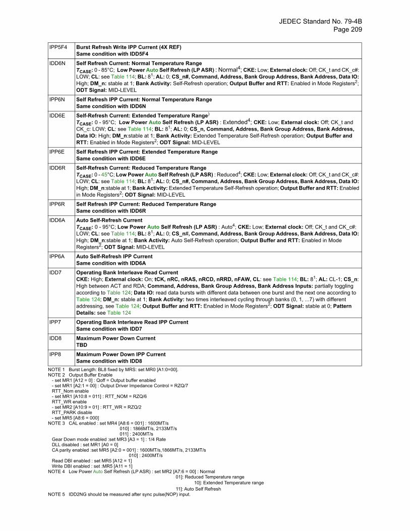
JEDEC Standard No. 79-4B Page 209
NOTE 1 Burst Length: BL8 fixed by MRS: set MR0 [A1:0=00]. NOTE 2 Output Buffer Enable - set MR1 [A12 = 0] : Qoff = Output buffer enabled - set MR1 [A2:1 = 00] : Output Driver Impedance Control = RZQ/7 RTT_Nom enable - set MR1 [A10:8 = 011] : RTT_NOM = RZQ/6 RTT_WR enable - set MR2 [A10:9 = 01] : RTT_WR = RZQ/2 RTT_PARK disable - set MR5 [A8:6 = 000] NOTE 3 CAL enabled : set MR4 [A8:6 = 001] : 1600MT/s 010] : 1866MT/s, 2133MT/s 011] : 2400MT/s Gear Down mode enabled :set MR3 [A3 = 1] : 1/4 Rate DLL disabled : set MR1 [A0 = 0] CA parity enabled :set MR5 [A2:0 = 001] : 1600MT/s,1866MT/s, 2133MT/s 010] : 2400MT/s Read DBI enabled : set MR5 [A12 = 1] Write DBI enabled : set :MR5 [A11 = 1]NOTE 4 Low Power Auto Self Refresh (LP ASR) : set MR2 [A7:6 = 00] : Normal 01]: Reduced Temperature range 10]: Extended Temperature range 11]: Auto Self Refresh NOTE 5 IDD2NG should be measured after sync pulse(NOP) input.
IPP5F4 Burst Refresh Write IPP Current (4X REF)Same condition with IDD5F4
IDD6N Self Refresh Current: Normal Temperature RangeTCASE: 0 - 85°C; Low Power Auto Self Refresh (LP ASR) : Normal4; CKE: Low; External clock: Off; CK_t and CK_c#: LOW; CL: see Table 114; BL: 81; AL: 0; CS_n#, Command, Address, Bank Group Address, Bank Address, Data IO: High; DM_n: stable at 1; Bank Activity: Self-Refresh operation; Output Buffer and RTT: Enabled in Mode Registers2; ODT Signal: MID-LEVEL
IPP6N Self Refresh IPP Current: Normal Temperature RangeSame condition with IDD6N
IDD6E Self-Refresh Current: Extended Temperature Range)
TCASE: 0 - 95°C; Low Power Auto Self Refresh (LP ASR) : Extended4; CKE: Low; External clock: Off; CK_t and CK_c: LOW; CL: see Table 114; BL: 81; AL: 0; CS_n, Command, Address, Bank Group Address, Bank Address, Data IO: High; DM_n:stable at 1; Bank Activity: Extended Temperature Self-Refresh operation; Output Buffer and RTT: Enabled in Mode Registers2; ODT Signal: MID-LEVEL
IPP6E Self Refresh IPP Current: Extended Temperature RangeSame condition with IDD6E
IDD6R Self-Refresh Current: Reduced Temperature RangeTCASE: 0 - 45°C; Low Power Auto Self Refresh (LP ASR) : Reduced4; CKE: Low; External clock: Off; CK_t and CK_c#: LOW; CL: see Table 114; BL: 81; AL: 0; CS_n#, Command, Address, Bank Group Address, Bank Address, Data IO: High; DM_n:stable at 1; Bank Activity: Extended Temperature Self-Refresh operation; Output Buffer and RTT: Enabled in Mode Registers2; ODT Signal: MID-LEVEL
IPP6R Self Refresh IPP Current: Reduced Temperature RangeSame condition with IDD6R
IDD6A Auto Self-Refresh CurrentTCASE: 0 - 95°C; Low Power Auto Self Refresh (LP ASR) : Auto4; CKE: Low; External clock: Off; CK_t and CK_c#: LOW; CL: see Table 114; BL: 81; AL: 0; CS_n#, Command, Address, Bank Group Address, Bank Address, Data IO: High; DM_n:stable at 1; Bank Activity: Auto Self-Refresh operation; Output Buffer and RTT: Enabled in Mode Registers2; ODT Signal: MID-LEVEL
IPP6A Auto Self-Refresh IPP CurrentSame condition with IDD6A
IDD7 Operating Bank Interleave Read CurrentCKE: High; External clock: On; tCK, nRC, nRAS, nRCD, nRRD, nFAW, CL: see Table 114; BL: 81; AL: CL-1; CS_n: High between ACT and RDA; Command, Address, Bank Group Address, Bank Address Inputs: partially toggling according to Table 124; Data IO: read data bursts with different data between one burst and the next one according to Table 124; DM_n: stable at 1; Bank Activity: two times interleaved cycling through banks (0, 1, ...7) with different addressing, see Table 124; Output Buffer and RTT: Enabled in Mode Registers2; ODT Signal: stable at 0; Pattern Details: see Table 124
IPP7 Operating Bank Interleave Read IPP CurrentSame condition with IDD7
IDD8 Maximum Power Down CurrentTBD
IPP8 Maximum Power Down IPP CurrentSame condition with IDD8
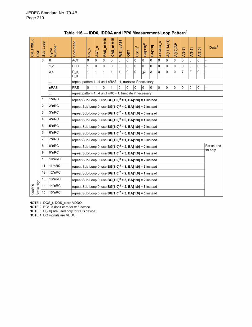
JEDEC Standard No. 79-4BPage 210
Table 116 — IDD0, IDD0A and IPP0 Measurement-Loop Pattern1
NOTE 1 DQS_t, DQS_c are VDDQ.NOTE 2 BG1 is don’t care for x16 device.NOTE 3 C[2:0] are used only for 3DS device.NOTE 4 DQ signals are VDDQ.
CK
_t /C
K_c
CK
E
Su
b-L
oo
p
Cyc
leN
um
be
r
Co
mm
and
CS
_n
AC
T_n
RA
S_n
/ A16
CA
S_n
/ A15
WE
_n/ A
14
OD
T
C[2
:0]3
BG
[1:0
]2
BA
[1:0
]
A12
/BC
_n
A[1
7,13
,11]
A[1
0]/A
P
A[9
:7]
A[6
:3]
A[2
:0] Data4
togg
ling
Sta
tic H
igh
0 0 ACT 0 0 0 0 0 0 0 0 0 0 0 0 0 0 0 -
1,2 D, D 1 0 0 0 0 0 0 0 0 0 0 0 0 0 0 -
3,4 D_#, D_#
1 1 1 1 1 0 0 32 3 0 0 0 7 F 0 -
... repeat pattern 1...4 until nRAS - 1, truncate if necessary
nRAS PRE 0 1 0 1 0 0 0 0 0 0 0 0 0 0 0 -
... repeat pattern 1...4 until nRC - 1, truncate if necessary
1 1*nRC repeat Sub-Loop 0, use BG[1:0]2 = 1, BA[1:0] = 1 instead
2 2*nRC repeat Sub-Loop 0, use BG[1:0]2 = 0, BA[1:0] = 2 instead
3 3*nRC repeat Sub-Loop 0, use BG[1:0]2 = 1, BA[1:0] = 3 instead
4 4*nRC repeat Sub-Loop 0, use BG[1:0]2 = 0, BA[1:0] = 1 instead
5 5*nRC repeat Sub-Loop 0, use BG[1:0]2 = 1, BA[1:0] = 2 instead
6 6*nRC repeat Sub-Loop 0, use BG[1:0]2 = 0, BA[1:0] = 3 instead
7 7*nRC repeat Sub-Loop 0, use BG[1:0]2 = 1, BA[1:0] = 0 instead
8 8*nRC repeat Sub-Loop 0, use BG[1:0]2 = 2, BA[1:0] = 0 instead For x4 and x8 only
9 9*nRC repeat Sub-Loop 0, use BG[1:0]2 = 3, BA[1:0] = 1 instead
10 10*nRC repeat Sub-Loop 0, use BG[1:0]2 = 2, BA[1:0] = 2 instead
11 11*nRC repeat Sub-Loop 0, use BG[1:0]2 = 3, BA[1:0] = 3 instead
12 12*nRC repeat Sub-Loop 0, use BG[1:0]2 = 2, BA[1:0] = 1 instead
13 13*nRC repeat Sub-Loop 0, use BG[1:0]2 = 3, BA[1:0] = 2 instead
14 14*nRC repeat Sub-Loop 0, use BG[1:0]2 = 2, BA[1:0] = 3 instead
15 15*nRC repeat Sub-Loop 0, use BG[1:0]2 = 3, BA[1:0] = 0 instead
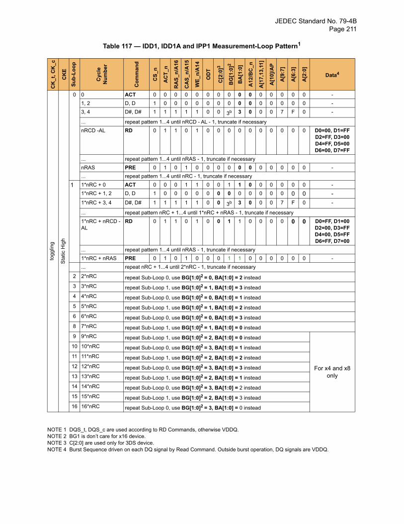
JEDEC Standard No. 79-4B Page 211
Table 117 — IDD1, IDD1A and IPP1 Measurement-Loop Pattern1
NOTE 1 DQS_t, DQS_c are used according to RD Commands, otherwise VDDQ.NOTE 2 BG1 is don’t care for x16 device.NOTE 3 C[2:0] are used only for 3DS device.NOTE 4 Burst Sequence driven on each DQ signal by Read Command. Outside burst operation, DQ signals are VDDQ.
CK
_t, C
K_c
CK
E
Su
b-L
oo
p
Cyc
leN
um
be
r
Co
mm
an
d
CS
_n
AC
T_n
RA
S_n
/A16
CA
S_n
/A15
WE
_n
/A1
4
OD
T
C[2
:0]3
BG
[1:0
]2
BA
[1:0
]
A12
/BC
_n
A[1
7,13
,11]
A[1
0]/A
P
A[9
:7]
A[6
:3]
A[2
:0]
Data4
togg
ling
Sta
tic H
igh
0 0 ACT 0 0 0 0 0 0 0 0 0 0 0 0 0 0 0 -
1, 2 D, D 1 0 0 0 0 0 0 0 0 0 0 0 0 0 0 -
3, 4 D#, D# 1 1 1 1 1 0 0 3b 3 0 0 0 7 F 0 -
... repeat pattern 1...4 until nRCD - AL - 1, truncate if necessary
nRCD -AL RD 0 1 1 0 1 0 0 0 0 0 0 0 0 0 0 D0=00, D1=FFD2=FF, D3=00D4=FF, D5=00D6=00, D7=FF
... repeat pattern 1...4 until nRAS - 1, truncate if necessary
nRAS PRE 0 1 0 1 0 0 0 0 0 0 0 0 0 0 0 -
... repeat pattern 1...4 until nRC - 1, truncate if necessary
1 1*nRC + 0 ACT 0 0 0 1 1 0 0 1 1 0 0 0 0 0 0 -
1*nRC + 1, 2 D, D 1 0 0 0 0 0 0 0 0 0 0 0 0 0 0 -
1*nRC + 3, 4 D#, D# 1 1 1 1 1 0 0 3b 3 0 0 0 7 F 0 -
... repeat pattern nRC + 1...4 until 1*nRC + nRAS - 1, truncate if necessary
1*nRC + nRCD - AL
RD 0 1 1 0 1 0 0 1 1 0 0 0 0 0 0 D0=FF, D1=00D2=00, D3=FFD4=00, D5=FFD6=FF, D7=00
... repeat pattern 1...4 until nRAS - 1, truncate if necessary
1*nRC + nRAS PRE 0 1 0 1 0 0 0 1 1 0 0 0 0 0 0 -
... repeat nRC + 1...4 until 2*nRC - 1, truncate if necessary
2 2*nRC repeat Sub-Loop 0, use BG[1:0]2 = 0, BA[1:0] = 2 instead
3 3*nRC repeat Sub-Loop 1, use BG[1:0]2 = 1, BA[1:0] = 3 instead
4 4*nRC repeat Sub-Loop 0, use BG[1:0]2 = 0, BA[1:0] = 1 instead
5 5*nRC repeat Sub-Loop 1, use BG[1:0]2 = 1, BA[1:0] = 2 instead
6 6*nRC repeat Sub-Loop 0, use BG[1:0]2 = 0, BA[1:0] = 3 instead
8 7*nRC repeat Sub-Loop 1, use BG[1:0]2 = 1, BA[1:0] = 0 instead
9 9*nRC repeat Sub-Loop 1, use BG[1:0]2 = 2, BA[1:0] = 0 instead
For x4 and x8 only
10 10*nRC repeat Sub-Loop 0, use BG[1:0]2 = 3, BA[1:0] = 1 instead
11 11*nRC repeat Sub-Loop 1, use BG[1:0]2 = 2, BA[1:0] = 2 instead
12 12*nRC repeat Sub-Loop 0, use BG[1:0]2 = 3, BA[1:0] = 3 instead
13 13*nRC repeat Sub-Loop 1, use BG[1:0]2 = 2, BA[1:0] = 1 instead
14 14*nRC repeat Sub-Loop 0, use BG[1:0]2 = 3, BA[1:0] = 2 instead
15 15*nRC repeat Sub-Loop 1, use BG[1:0]2 = 2, BA[1:0] = 3 instead
16 16*nRC repeat Sub-Loop 0, use BG[1:0]2 = 3, BA[1:0] = 0 instead
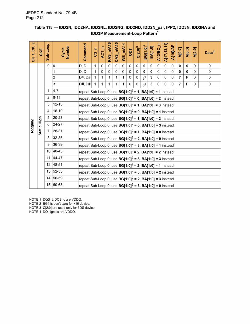
JEDEC Standard No. 79-4BPage 212
Table 118 — IDD2N, IDD2NA, IDD2NL, IDD2NG, IDD2ND, IDD2N_par, IPP2, IDD3N, IDD3NA and
IDD3P Measurement-Loop Pattern1
NOTE 1 DQS_t, DQS_c are VDDQ.NOTE 2 BG1 is don’t care for x16 device.NOTE 3 C[2:0] are used only for 3DS device.NOTE 4 DQ signals are VDDQ.
CK
_t,
CK
_c
CK
E
Su
b-L
oo
p
Cyc
leN
um
be
r
Co
mm
and
CS
_n
AC
T_
n
RA
S_
n/A
16
CA
S_
n/A
15
WE
_n/A
14
OD
T
C[2
:0]3
BG
[1:0
]2
BA
[1:0
]
A1
2/B
C_n
A[1
7,13
,11]
A[1
0]/A
P
A[9
:7]
A[6
:3]
A[2
:0]
Data4
tog
gli
ng
Sta
tic
Hig
h
0 0 D, D 1 0 0 0 0 0 0 0 0 0 0 0 0 0 0 0
1 D, D 1 0 0 0 0 0 0 0 0 0 0 0 0 0 0 0
2 D#, D# 1 1 1 1 1 0 0 32 3 0 0 0 7 F 0 0
3 D#, D# 1 1 1 1 1 0 0 32 3 0 0 0 7 F 0 0
1 4-7 repeat Sub-Loop 0, use BG[1:0]2 = 1, BA[1:0] = 1 instead
2 8-11 repeat Sub-Loop 0, use BG[1:0]2 = 0, BA[1:0] = 2 instead
3 12-15 repeat Sub-Loop 0, use BG[1:0]2 = 1, BA[1:0] = 3 instead
4 16-19 repeat Sub-Loop 0, use BG[1:0]2 = 0, BA[1:0] = 1 instead
5 20-23 repeat Sub-Loop 0, use BG[1:0]2 = 1, BA[1:0] = 2 instead
6 24-27 repeat Sub-Loop 0, use BG[1:0]2 = 0, BA[1:0] = 3 instead
7 28-31 repeat Sub-Loop 0, use BG[1:0]2 = 1, BA[1:0] = 0 instead
8 32-35 repeat Sub-Loop 0, use BG[1:0]2 = 2, BA[1:0] = 0 instead
9 36-39 repeat Sub-Loop 0, use BG[1:0]2 = 3, BA[1:0] = 1 instead
10 40-43 repeat Sub-Loop 0, use BG[1:0]2 = 2, BA[1:0] = 2 instead
11 44-47 repeat Sub-Loop 0, use BG[1:0]2 = 3, BA[1:0] = 3 instead
12 48-51 repeat Sub-Loop 0, use BG[1:0]2 = 2, BA[1:0] = 1 instead
13 52-55 repeat Sub-Loop 0, use BG[1:0]2 = 3, BA[1:0] = 2 instead
14 56-59 repeat Sub-Loop 0, use BG[1:0]2 = 2, BA[1:0] = 3 instead
15 60-63 repeat Sub-Loop 0, use BG[1:0]2 = 3, BA[1:0] = 0 instead
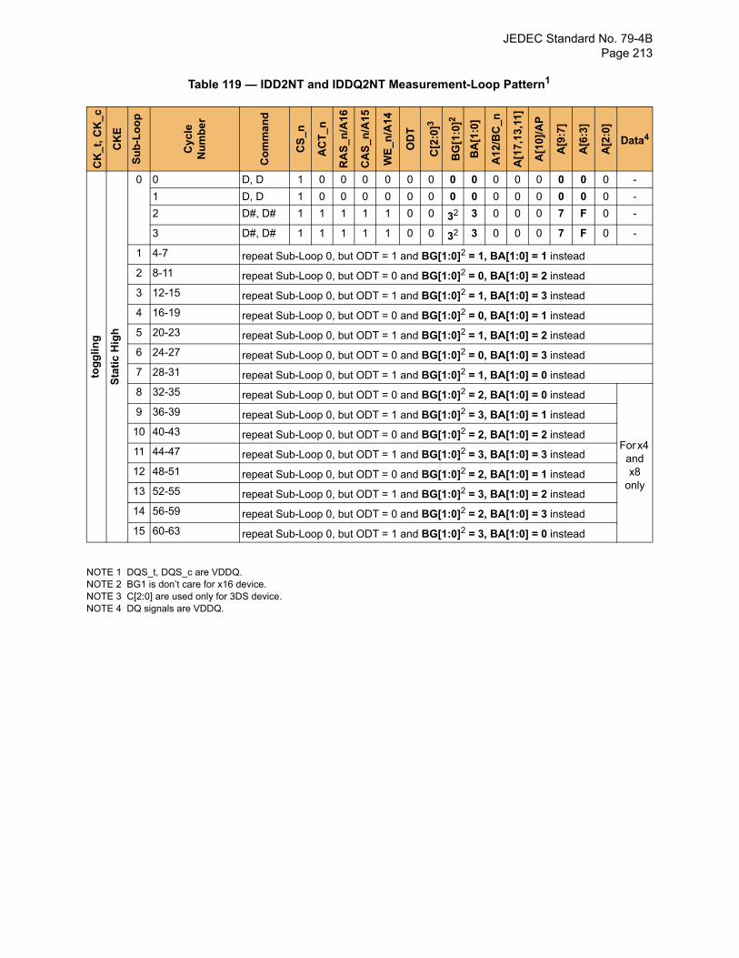
JEDEC Standard No. 79-4B Page 213
Table 119 — IDD2NT and IDDQ2NT Measurement-Loop Pattern1
NOTE 1 DQS_t, DQS_c are VDDQ.NOTE 2 BG1 is don’t care for x16 device.NOTE 3 C[2:0] are used only for 3DS device.NOTE 4 DQ signals are VDDQ.
CK
_t,
CK
_c
CK
E
Su
b-L
oo
p
Cy
cle
Nu
mb
er
Co
mm
and
CS
_n
AC
T_
n
RA
S_
n/A
16
CA
S_
n/A
15
WE
_n/A
14
OD
T
C[2
:0]3
BG
[1:0
]2
BA
[1:0
]
A1
2/B
C_n
A[1
7,13
,11]
A[1
0]/A
P
A[9
:7]
A[6
:3]
A[2
:0]
Data4
tog
glin
g
Sta
tic
Hig
h
0 0 D, D 1 0 0 0 0 0 0 0 0 0 0 0 0 0 0 -
1 D, D 1 0 0 0 0 0 0 0 0 0 0 0 0 0 0 -
2 D#, D# 1 1 1 1 1 0 0 32 3 0 0 0 7 F 0 -
3 D#, D# 1 1 1 1 1 0 0 32 3 0 0 0 7 F 0 -
1 4-7 repeat Sub-Loop 0, but ODT = 1 and BG[1:0]2 = 1, BA[1:0] = 1 instead
2 8-11 repeat Sub-Loop 0, but ODT = 0 and BG[1:0]2 = 0, BA[1:0] = 2 instead
3 12-15 repeat Sub-Loop 0, but ODT = 1 and BG[1:0]2 = 1, BA[1:0] = 3 instead
4 16-19 repeat Sub-Loop 0, but ODT = 0 and BG[1:0]2 = 0, BA[1:0] = 1 instead
5 20-23 repeat Sub-Loop 0, but ODT = 1 and BG[1:0]2 = 1, BA[1:0] = 2 instead
6 24-27 repeat Sub-Loop 0, but ODT = 0 and BG[1:0]2 = 0, BA[1:0] = 3 instead
7 28-31 repeat Sub-Loop 0, but ODT = 1 and BG[1:0]2 = 1, BA[1:0] = 0 instead
8 32-35 repeat Sub-Loop 0, but ODT = 0 and BG[1:0]2 = 2, BA[1:0] = 0 instead
For x4 and x8
only
9 36-39 repeat Sub-Loop 0, but ODT = 1 and BG[1:0]2 = 3, BA[1:0] = 1 instead
10 40-43 repeat Sub-Loop 0, but ODT = 0 and BG[1:0]2 = 2, BA[1:0] = 2 instead
11 44-47 repeat Sub-Loop 0, but ODT = 1 and BG[1:0]2 = 3, BA[1:0] = 3 instead
12 48-51 repeat Sub-Loop 0, but ODT = 0 and BG[1:0]2 = 2, BA[1:0] = 1 instead
13 52-55 repeat Sub-Loop 0, but ODT = 1 and BG[1:0]2 = 3, BA[1:0] = 2 instead
14 56-59 repeat Sub-Loop 0, but ODT = 0 and BG[1:0]2 = 2, BA[1:0] = 3 instead
15 60-63 repeat Sub-Loop 0, but ODT = 1 and BG[1:0]2 = 3, BA[1:0] = 0 instead
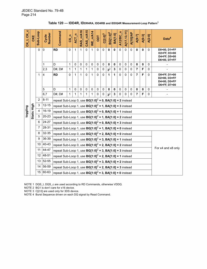
JEDEC Standard No. 79-4BPage 214
Table 120 — IDD4R, IDDR4RA, IDD4RB and IDDQ4R Measurement-Loop Pattern1
NOTE 1 DQS_t, DQS_c are used according to RD Commands, otherwise VDDQ.NOTE 2 BG1 is don’t care for x16 device.NOTE 3 C[2:0] are used only for 3DS device.NOTE 4 Burst Sequence driven on each DQ signal by Read Command.
CK
_t, C
K_
c
CK
E
Su
b-L
oo
p
Cy
cle
Nu
mb
er
Co
mm
and
CS
_n
AC
T_n
RA
S_n
/A16
CA
S_n
/A15
WE
_n/A
14
OD
T
C[2
:0]3
BG
[1:0
]2
BA
[1:0
]
A1
2/B
C_n
A[1
7,13
,11
]
A[1
0]/
AP
A[9
:7]
A[6
:3]
A[2
:0]
Data4
tog
glin
g
Sta
tic
Hig
h
0 0 RD 0 1 1 0 1 0 0 0 0 0 0 0 0 0 0 D0=00, D1=FFD2=FF, D3=00D4=FF, D5=00D6=00, D7=FF
1 D 1 0 0 0 0 0 0 0 0 0 0 0 0 0 0 -
2,3 D#, D# 1 1 1 1 1 0 0 32 3 0 0 0 7 F 0 -
1 4 RD 0 1 1 0 1 0 0 1 1 0 0 0 7 F 0 D0=FF, D1=00D2=00, D3=FFD4=00, D5=FFD6=FF, D7=00
5 D 1 0 0 0 0 0 0 0 0 0 0 0 0 0 0 -
6,7 D#, D# 1 1 1 1 1 0 0 32 3 0 0 0 7 F 0 -
2 8-11 repeat Sub-Loop 0, use BG[1:0]2 = 0, BA[1:0] = 2 instead
3 12-15 repeat Sub-Loop 1, use BG[1:0]2 = 1, BA[1:0] = 3 instead
4 16-19 repeat Sub-Loop 0, use BG[1:0]2 = 0, BA[1:0] = 1 instead
5 20-23 repeat Sub-Loop 1, use BG[1:0]2 = 1, BA[1:0] = 2 instead
6 24-27 repeat Sub-Loop 0, use BG[1:0]2 = 0, BA[1:0] = 3 instead
7 28-31 repeat Sub-Loop 1, use BG[1:0]2 = 1, BA[1:0] = 0 instead
8 32-35 repeat Sub-Loop 0, use BG[1:0]2 = 2, BA[1:0] = 0 instead
For x4 and x8 only
9 36-39 repeat Sub-Loop 1, use BG[1:0]2 = 3, BA[1:0] = 1 instead
10 40-43 repeat Sub-Loop 0, use BG[1:0]2 = 2, BA[1:0] = 2 instead
11 44-47 repeat Sub-Loop 1, use BG[1:0]2 = 3, BA[1:0] = 3 instead
12 48-51 repeat Sub-Loop 0, use BG[1:0]2 = 2, BA[1:0] = 1 instead
13 52-55 repeat Sub-Loop 1, use BG[1:0]2 = 3, BA[1:0] = 2 instead
14 56-59 repeat Sub-Loop 0, use BG[1:0]2 = 2, BA[1:0] = 3 instead
15 60-63 repeat Sub-Loop 1, use BG[1:0]2 = 3, BA[1:0] = 0 instead
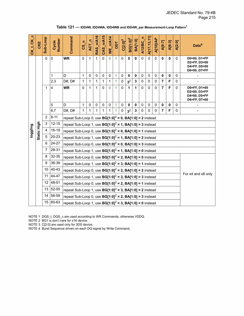
JEDEC Standard No. 79-4B Page 215
Table 121 — IDD4W, IDD4WA, IDD4WB and IDD4W_par Measurement-Loop Pattern1
NOTE 1 DQS_t, DQS_c are used according to WR Commands, otherwise VDDQ.NOTE 2 BG1 is don’t care for x16 device.NOTE 3 C[2:0] are used only for 3DS device.NOTE 4 Burst Sequence driven on each DQ signal by Write Command.
CK
_t, C
K_
c
CK
E
Su
b-L
oo
p
Cy
cle
Nu
mb
er
Co
mm
and
CS
_n
AC
T_n
RA
S_n
/A16
CA
S_n
/A15
WE
_n/A
14
OD
T
C[2
:0]3
BG
[1:0
]2
BA
[1:0
]
A1
2/B
C_n
A[1
7,13
,11
]
A[1
0]/
AP
A[9
:7]
A[6
:3]
A[2
:0]
Data4
tog
glin
g
Sta
tic
Hig
h
0 0 WR 0 1 1 0 0 1 0 0 0 0 0 0 0 0 0 D0=00, D1=FFD2=FF, D3=00D4=FF, D5=00D6=00, D7=FF
1 D 1 0 0 0 0 1 0 0 0 0 0 0 0 0 0 -
2,3 D#, D# 1 1 1 1 1 1 0 32 3 0 0 0 7 F 0 -
1 4 WR 0 1 1 0 0 1 0 1 1 0 0 0 7 F 0 D0=FF, D1=00D2=00, D3=FFD4=00, D5=FFD6=FF, D7=00
5 D 1 0 0 0 0 1 0 0 0 0 0 0 0 0 0 -
6,7 D#, D# 1 1 1 1 1 1 0 32 3 0 0 0 7 F 0 -
2 8-11 repeat Sub-Loop 0, use BG[1:0]2 = 0, BA[1:0] = 2 instead
3 12-15 repeat Sub-Loop 1, use BG[1:0]2 = 1, BA[1:0] = 3 instead
4 16-19 repeat Sub-Loop 0, use BG[1:0]2 = 0, BA[1:0] = 1 instead
5 20-23 repeat Sub-Loop 1, use BG[1:0]2 = 1, BA[1:0] = 2 instead
6 24-27 repeat Sub-Loop 0, use BG[1:0]2 = 0, BA[1:0] = 3 instead
7 28-31 repeat Sub-Loop 1, use BG[1:0]2 = 1, BA[1:0] = 0 instead
8 32-35 repeat Sub-Loop 0, use BG[1:0]2 = 2, BA[1:0] = 0 instead
For x4 and x8 only
9 36-39 repeat Sub-Loop 1, use BG[1:0]2 = 3, BA[1:0] = 1 instead
10 40-43 repeat Sub-Loop 0, use BG[1:0]2 = 2, BA[1:0] = 2 instead
11 44-47 repeat Sub-Loop 1, use BG[1:0]2 = 3, BA[1:0] = 3 instead
12 48-51 repeat Sub-Loop 0, use BG[1:0]2 = 2, BA[1:0] = 1 instead
13 52-55 repeat Sub-Loop 1, use BG[1:0]2 = 3, BA[1:0] = 2 instead
14 56-59 repeat Sub-Loop 0, use BG[1:0]2 = 2, BA[1:0] = 3 instead
15 60-63 repeat Sub-Loop 1, use BG[1:0]2 = 3, BA[1:0] = 0 instead
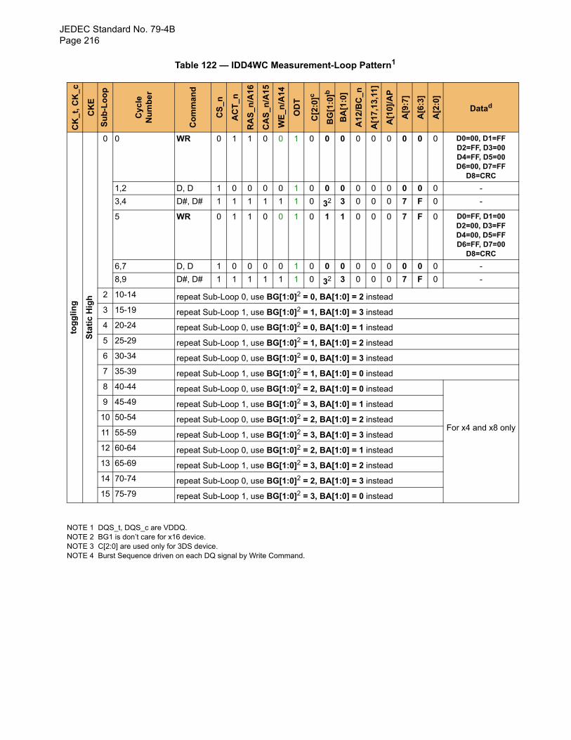
JEDEC Standard No. 79-4BPage 216
Table 122 — IDD4WC Measurement-Loop Pattern1
NOTE 1 DQS_t, DQS_c are VDDQ.NOTE 2 BG1 is don’t care for x16 device.NOTE 3 C[2:0] are used only for 3DS device.NOTE 4 Burst Sequence driven on each DQ signal by Write Command.
CK
_t,
CK
_c
CK
E
Su
b-L
oo
p
Cy
cle
Nu
mb
er
Co
mm
and
CS
_n
AC
T_
n
RA
S_
n/A
16
CA
S_
n/A
15
WE
_n/A
14
OD
T
C[2
:0]c
BG
[1:0
]b
BA
[1:0
]
A1
2/B
C_n
A[1
7,13
,11]
A[1
0]/A
P
A[9
:7]
A[6
:3]
A[2
:0]
Datad
tog
glin
g
Sta
tic
Hig
h
0 0 WR 0 1 1 0 0 1 0 0 0 0 0 0 0 0 0 D0=00, D1=FFD2=FF, D3=00D4=FF, D5=00D6=00, D7=FF
D8=CRC
1,2 D, D 1 0 0 0 0 1 0 0 0 0 0 0 0 0 0 -
3,4 D#, D# 1 1 1 1 1 1 0 32 3 0 0 0 7 F 0 -
5 WR 0 1 1 0 0 1 0 1 1 0 0 0 7 F 0 D0=FF, D1=00D2=00, D3=FFD4=00, D5=FFD6=FF, D7=00
D8=CRC
6,7 D, D 1 0 0 0 0 1 0 0 0 0 0 0 0 0 0 -
8,9 D#, D# 1 1 1 1 1 1 0 32 3 0 0 0 7 F 0 -
2 10-14 repeat Sub-Loop 0, use BG[1:0]2 = 0, BA[1:0] = 2 instead
3 15-19 repeat Sub-Loop 1, use BG[1:0]2 = 1, BA[1:0] = 3 instead
4 20-24 repeat Sub-Loop 0, use BG[1:0]2 = 0, BA[1:0] = 1 instead
5 25-29 repeat Sub-Loop 1, use BG[1:0]2 = 1, BA[1:0] = 2 instead
6 30-34 repeat Sub-Loop 0, use BG[1:0]2 = 0, BA[1:0] = 3 instead
7 35-39 repeat Sub-Loop 1, use BG[1:0]2 = 1, BA[1:0] = 0 instead
8 40-44 repeat Sub-Loop 0, use BG[1:0]2 = 2, BA[1:0] = 0 instead
For x4 and x8 only
9 45-49 repeat Sub-Loop 1, use BG[1:0]2 = 3, BA[1:0] = 1 instead
10 50-54 repeat Sub-Loop 0, use BG[1:0]2 = 2, BA[1:0] = 2 instead
11 55-59 repeat Sub-Loop 1, use BG[1:0]2 = 3, BA[1:0] = 3 instead
12 60-64 repeat Sub-Loop 0, use BG[1:0]2 = 2, BA[1:0] = 1 instead
13 65-69 repeat Sub-Loop 1, use BG[1:0]2 = 3, BA[1:0] = 2 instead
14 70-74 repeat Sub-Loop 0, use BG[1:0]2 = 2, BA[1:0] = 3 instead
15 75-79 repeat Sub-Loop 1, use BG[1:0]2 = 3, BA[1:0] = 0 instead
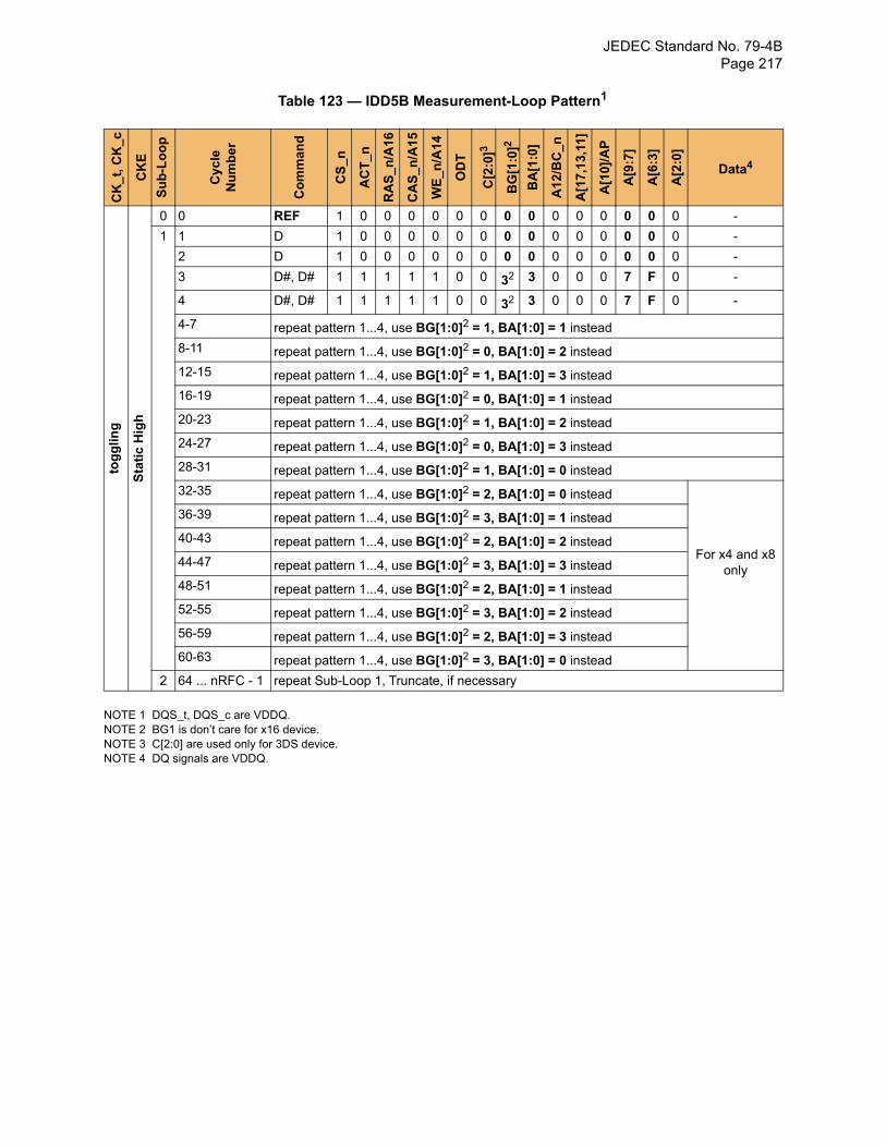
JEDEC Standard No. 79-4B Page 217
Table 123 — IDD5B Measurement-Loop Pattern1
NOTE 1 DQS_t, DQS_c are VDDQ.NOTE 2 BG1 is don’t care for x16 device.NOTE 3 C[2:0] are used only for 3DS device.NOTE 4 DQ signals are VDDQ.
CK
_t,
CK
_c
CK
E
Su
b-L
oo
p
Cyc
leN
um
be
r
Co
mm
and
CS
_n
AC
T_
n
RA
S_
n/A
16
CA
S_
n/A
15
WE
_n/A
14
OD
T
C[2
:0]3
BG
[1:0
]2
BA
[1:0
]
A1
2/B
C_n
A[1
7,13
,11]
A[1
0]/A
P
A[9
:7]
A[6
:3]
A[2
:0]
Data4
tog
glin
g
Sta
tic
Hig
h
0 0 REF 1 0 0 0 0 0 0 0 0 0 0 0 0 0 0 -
1 1 D 1 0 0 0 0 0 0 0 0 0 0 0 0 0 0 -
2 D 1 0 0 0 0 0 0 0 0 0 0 0 0 0 0 -
3 D#, D# 1 1 1 1 1 0 0 32 3 0 0 0 7 F 0 -
4 D#, D# 1 1 1 1 1 0 0 32 3 0 0 0 7 F 0 -
4-7 repeat pattern 1...4, use BG[1:0]2 = 1, BA[1:0] = 1 instead
8-11 repeat pattern 1...4, use BG[1:0]2 = 0, BA[1:0] = 2 instead
12-15 repeat pattern 1...4, use BG[1:0]2 = 1, BA[1:0] = 3 instead
16-19 repeat pattern 1...4, use BG[1:0]2 = 0, BA[1:0] = 1 instead
20-23 repeat pattern 1...4, use BG[1:0]2 = 1, BA[1:0] = 2 instead
24-27 repeat pattern 1...4, use BG[1:0]2 = 0, BA[1:0] = 3 instead
28-31 repeat pattern 1...4, use BG[1:0]2 = 1, BA[1:0] = 0 instead
32-35 repeat pattern 1...4, use BG[1:0]2 = 2, BA[1:0] = 0 instead
For x4 and x8 only
36-39 repeat pattern 1...4, use BG[1:0]2 = 3, BA[1:0] = 1 instead
40-43 repeat pattern 1...4, use BG[1:0]2 = 2, BA[1:0] = 2 instead
44-47 repeat pattern 1...4, use BG[1:0]2 = 3, BA[1:0] = 3 instead
48-51 repeat pattern 1...4, use BG[1:0]2 = 2, BA[1:0] = 1 instead
52-55 repeat pattern 1...4, use BG[1:0]2 = 3, BA[1:0] = 2 instead
56-59 repeat pattern 1...4, use BG[1:0]2 = 2, BA[1:0] = 3 instead
60-63 repeat pattern 1...4, use BG[1:0]2 = 3, BA[1:0] = 0 instead
2 64 ... nRFC - 1 repeat Sub-Loop 1, Truncate, if necessary
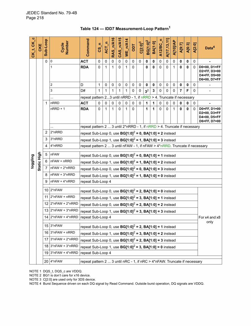
JEDEC Standard No. 79-4BPage 218
Table 124 — IDD7 Measurement-Loop Pattern1
NOTE 1 DQS_t, DQS_c are VDDQ.NOTE 2 BG1 is don’t care for x16 device.NOTE 3 C[2:0] are used only for 3DS device.NOTE 4 Burst Sequence driven on each DQ signal by Read Command. Outside burst operation, DQ signals are VDDQ.
CK
_t,
CK
_c
CK
E
Su
b-L
oo
p
Cyc
leN
um
be
r
Co
mm
and
CS
_n
AC
T_
n
RA
S_
n/A
16
CA
S_
n/A
15
WE
_n/A
14
OD
T
C[2
:0]3
BG
[1:0
]2
BA
[1:0
]
A1
2/B
C_n
A[1
7,13
,11]
A[1
0]/A
P
A[9
:7]
A[6
:3]
A[2
:0]
Data4
tog
gli
ng
Sta
tic
Hig
h
0 0 ACT 0 0 0 0 0 0 0 0 0 0 0 0 0 0 0 -
1 RDA 0 1 1 0 1 0 0 0 0 0 1 0 0 0 D0=00, D1=FFD2=FF, D3=00D4=FF, D5=00D6=00, D7=FF
2 D 1 0 0 0 0 0 0 0 0 0 0 0 0 0 0 -
3 D# 1 1 1 1 1 0 0 32 3 0 0 0 7 F 0 -
... repeat pattern 2...3 until nRRD - 1, if nRRD > 4. Truncate if necessary
1 nRRD ACT 0 0 0 0 0 0 0 1 1 0 0 0 0 0 0 -
nRRD + 1 RDA 0 1 1 0 1 0 1 1 0 0 1 0 0 0 D0=FF, D1=00D2=00, D3=FFD4=00, D5=FFD6=FF, D7=00
... repeat pattern 2 ... 3 until 2*nRRD - 1, if nRRD > 4. Truncate if necessary
2 2*nRRD repeat Sub-Loop 0, use BG[1:0]2 = 0, BA[1:0] = 2 instead
3 3*nRRD repeat Sub-Loop 1, use BG[1:0]2 = 1, BA[1:0] = 3 instead
4 4*nRRD repeat pattern 2 ... 3 until nFAW - 1, if nFAW > 4*nRRD. Truncate if necessary
5 nFAW repeat Sub-Loop 0, use BG[1:0]2 = 0, BA[1:0] = 1 instead
6 nFAW + nRRD repeat Sub-Loop 1, use BG[1:0]2 = 1, BA[1:0] = 2 instead
7 nFAW + 2*nRRD repeat Sub-Loop 0, use BG[1:0]2 = 0, BA[1:0] = 3 instead
8 nFAW + 3*nRRD repeat Sub-Loop 1, use BG[1:0]2 = 1, BA[1:0] = 0 instead
9 nFAW + 4*nRRD repeat Sub-Loop 4
10 2*nFAW repeat Sub-Loop 0, use BG[1:0]2 = 2, BA[1:0] = 0 instead
For x4 and x8 only
11 2*nFAW + nRRD repeat Sub-Loop 1, use BG[1:0]2 = 3, BA[1:0] = 1 instead
12 2*nFAW + 2*nRRD repeat Sub-Loop 0, use BG[1:0]2 = 2, BA[1:0] = 2 instead
13 2*nFAW + 3*nRRD repeat Sub-Loop 1, use BG[1:0]2 = 3, BA[1:0] = 3 instead
14 2*nFAW + 4*nRRD repeat Sub-Loop 4
15 3*nFAW repeat Sub-Loop 0, use BG[1:0]2 = 2, BA[1:0] = 1 instead
16 3*nFAW + nRRD repeat Sub-Loop 1, use BG[1:0]2 = 3, BA[1:0] = 2 instead
17 3*nFAW + 2*nRRD repeat Sub-Loop 0, use BG[1:0]2 = 2, BA[1:0] = 3 instead
18 3*nFAW + 3*nRRD repeat Sub-Loop 1, use BG[1:0]2 = 3, BA[1:0] = 0 instead
19 3*nFAW + 4*nRRD repeat Sub-Loop 4
20 4*nFAW repeat pattern 2 ... 3 until nRC - 1, if nRC > 4*nFAW. Truncate if necessary
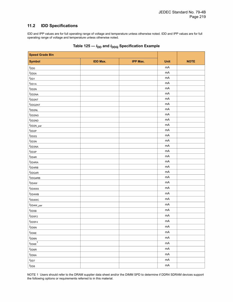
JEDEC Standard No. 79-4B Page 219
11.2 IDD Specifications
IDD and IPP values are for full operating range of voltage and temperature unless otherwise noted. IDD and IPP values are for full operating range of voltage and temperature unless otherwise noted.
Table 125 — IDD and IDDQ Specification Example
NOTE 1 Users should refer to the DRAM supplier data sheet and/or the DIMM SPD to determine if DDR4 SDRAM devices support the following options or requirements referred to in this material.
Speed Grade Bin
Unit NOTESymbol IDD Max. IPP Max.
IDD0 mA
IDD0A mA
IDD1 mA
IDD1A mA
IDD2N mA
IDD2NA mA
IDD2NT mA
IDDQ2NT mA
IDD2NL mA
IDD2NG mA
IDD2ND mA
IDD2N_par mA
IDD2P mA
IDD2Q mA
IDD3N mA
IDD3NA mA
IDD3P mA
IDD4R mA
IDD4RA mA
IDD4RB mA
IDDQ4R mA
IDDQ4RB mA
IDD4W mA
IDD4WA mA
IDD4WB mA
IDD4WC mA
IDD4W_par mA
IDD5B mA
IDD5F2 mA
IDD5F4 mA
IDD6N mA
IDD6E mA
IDD6N mA
IDD6E1 mA
IDD6R mA
IDD6A mA
IDD7 mA
IDD8 mA
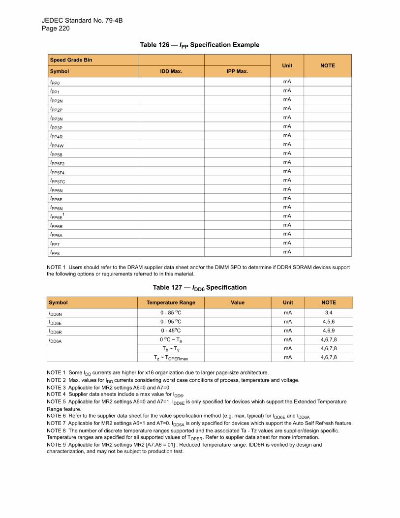
JEDEC Standard No. 79-4BPage 220
Table 126 — IPP Specification Example
NOTE 1 Users should refer to the DRAM supplier data sheet and/or the DIMM SPD to determine if DDR4 SDRAM devices support the following options or requirements referred to in this material.
Table 127 — IDD6 Specification
NOTE 1 Some IDD currents are higher for x16 organization due to larger page-size architecture.
NOTE 2 Max. values for IDD currents considering worst case conditions of process, temperature and voltage.
NOTE 3 Applicable for MR2 settings A6=0 and A7=0.NOTE 4 Supplier data sheets include a max value for IDD6.
NOTE 5 Applicable for MR2 settings A6=0 and A7=1. IDD6E is only specified for devices which support the Extended Temperature
Range feature.NOTE 6 Refer to the supplier data sheet for the value specification method (e.g. max, typical) for IDD6E and IDD6A
NOTE 7 Applicable for MR2 settings A6=1 and A7=0. IDD6A is only specified for devices which support the Auto Self Refresh feature.
NOTE 8 The number of discrete temperature ranges supported and the associated Ta - Tz values are supplier/design specific. Temperature ranges are specified for all supported values of TOPER. Refer to supplier data sheet for more information.
NOTE 9 Applicable for MR2 settings MR2 [A7:A6 = 01] : Reduced Temperature range. IDD6R is verified by design and characterization, and may not be subject to production test.
Speed Grade BinUnit NOTE
Symbol IDD Max. IPP Max.
IPP0 mA
IPP1 mA
IPP2N mA
IPP2P mA
IPP3N mA
IPP3P mA
IPP4R mA
IPP4W mA
IPP5B mA
IPP5F2 mA
IPP5F4 mA
IPP5TC mA
IPP6N mA
IPP6E mA
IPP6N mA
IPP6E1 mA
IPP6R mA
IPP6A mA
IPP7 mA
IPP8 mA
Symbol Temperature Range Value Unit NOTE
IDD6N 0 - 85 oC mA 3,4
IDD6E 0 - 95 oC mA 4,5,6
IDD6R 0 - 45oC mA 4,6,9
IDD6A 0 oC ~ Ta mA 4,6,7,8
Tb ~ Ty mA 4,6,7,8
Tz ~ TOPERmax mA 4,6,7,8
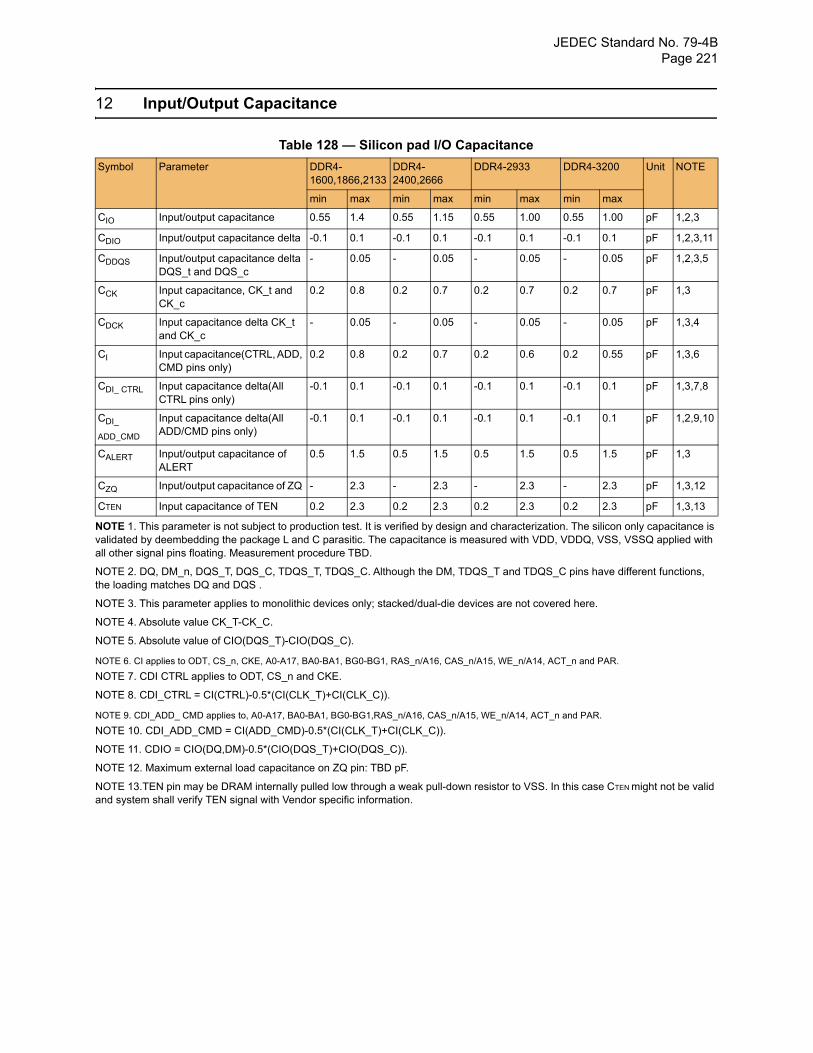
JEDEC Standard No. 79-4B Page 221
12 Input/Output Capacitance
Table 128 — Silicon pad I/O Capacitance
NOTE 1. This parameter is not subject to production test. It is verified by design and characterization. The silicon only capacitance is validated by deembedding the package L and C parasitic. The capacitance is measured with VDD, VDDQ, VSS, VSSQ applied with all other signal pins floating. Measurement procedure TBD.
NOTE 2. DQ, DM_n, DQS_T, DQS_C, TDQS_T, TDQS_C. Although the DM, TDQS_T and TDQS_C pins have different functions, the loading matches DQ and DQS .
NOTE 3. This parameter applies to monolithic devices only; stacked/dual-die devices are not covered here.
NOTE 4. Absolute value CK_T-CK_C.
NOTE 5. Absolute value of CIO(DQS_T)-CIO(DQS_C).
NOTE 6. CI applies to ODT, CS_n, CKE, A0-A17, BA0-BA1, BG0-BG1, RAS_n/A16, CAS_n/A15, WE_n/A14, ACT_n and PAR.
NOTE 7. CDI CTRL applies to ODT, CS_n and CKE.
NOTE 8. CDI_CTRL = CI(CTRL)-0.5*(CI(CLK_T)+CI(CLK_C)).
NOTE 9. CDI_ADD_ CMD applies to, A0-A17, BA0-BA1, BG0-BG1,RAS_n/A16, CAS_n/A15, WE_n/A14, ACT_n and PAR.
NOTE 10. CDI_ADD_CMD = CI(ADD_CMD)-0.5*(CI(CLK_T)+CI(CLK_C)).
NOTE 11. CDIO = CIO(DQ,DM)-0.5*(CIO(DQS_T)+CIO(DQS_C)).
NOTE 12. Maximum external load capacitance on ZQ pin: TBD pF.
NOTE 13.TEN pin may be DRAM internally pulled low through a weak pull-down resistor to VSS. In this case CTEN might not be valid and system shall verify TEN signal with Vendor specific information.
Symbol Parameter DDR4-1600,1866,2133
DDR4-2400,2666
DDR4-2933 DDR4-3200 Unit NOTE
min max min max min max min max
CIO Input/output capacitance 0.55 1.4 0.55 1.15 0.55 1.00 0.55 1.00 pF 1,2,3
CDIO Input/output capacitance delta -0.1 0.1 -0.1 0.1 -0.1 0.1 -0.1 0.1 pF 1,2,3,11
CDDQS Input/output capacitance delta DQS_t and DQS_c
- 0.05 - 0.05 - 0.05 - 0.05 pF 1,2,3,5
CCK Input capacitance, CK_t and CK_c
0.2 0.8 0.2 0.7 0.2 0.7 0.2 0.7 pF 1,3
CDCK Input capacitance delta CK_t and CK_c
- 0.05 - 0.05 - 0.05 - 0.05 pF 1,3,4
CI Input capacitance(CTRL, ADD, CMD pins only)
0.2 0.8 0.2 0.7 0.2 0.6 0.2 0.55 pF 1,3,6
CDI_ CTRL Input capacitance delta(All CTRL pins only)
-0.1 0.1 -0.1 0.1 -0.1 0.1 -0.1 0.1 pF 1,3,7,8
CDI_
ADD_CMD
Input capacitance delta(All ADD/CMD pins only)
-0.1 0.1 -0.1 0.1 -0.1 0.1 -0.1 0.1 pF 1,2,9,10
CALERT Input/output capacitance of ALERT
0.5 1.5 0.5 1.5 0.5 1.5 0.5 1.5 pF 1,3
CZQ Input/output capacitance of ZQ - 2.3 - 2.3 - 2.3 - 2.3 pF 1,3,12
CTEN Input capacitance of TEN 0.2 2.3 0.2 2.3 0.2 2.3 0.2 2.3 pF 1,3,13
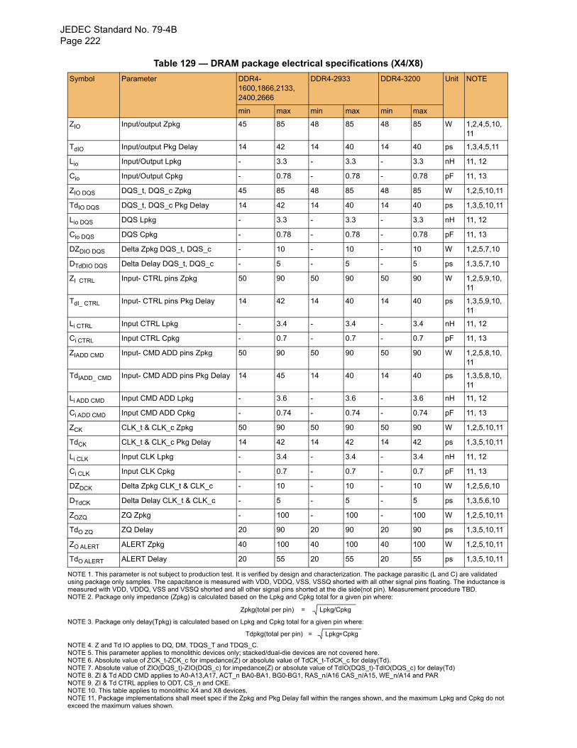
JEDEC Standard No. 79-4BPage 222
Table 129 — DRAM package electrical specifications (X4/X8)
NOTE 1. This parameter is not subject to production test. It is verified by design and characterization. The package parasitic (L and C) are validated using package only samples. The capacitance is measured with VDD, VDDQ, VSS, VSSQ shorted with all other signal pins floating. The inductance is measured with VDD, VDDQ, VSS and VSSQ shorted and all other signal pins shorted at the die side(not pin). Measurement procedure TBD. NOTE 2. Package only impedance (Zpkg) is calculated based on the Lpkg and Cpkg total for a given pin where:
NOTE 3. Package only delay(Tpkg) is calculated based on Lpkg and Cpkg total for a given pin where:
NOTE 4. Z and Td IO applies to DQ, DM, TDQS_T and TDQS_C. NOTE 5. This parameter applies to monolithic devices only; stacked/dual-die devices are not covered here. NOTE 6. Absolute value of ZCK_t-ZCK_c for impedance(Z) or absolute value of TdCK_t-TdCK_c for delay(Td). NOTE 7. Absolute value of ZIO(DQS_t)-ZIO(DQS_c) for impedance(Z) or absolute value of TdIO(DQS_t)-TdIO(DQS_c) for delay(Td) NOTE 8. ZI & Td ADD CMD applies to A0-A13,A17, ACT_n BA0-BA1, BG0-BG1, RAS_n/A16 CAS_n/A15, WE_n/A14 and PARNOTE 9. ZI & Td CTRL applies to ODT, CS_n and CKE.NOTE 10. This table applies to monolithic X4 and X8 devices. NOTE 11. Package implementations shall meet spec if the Zpkg and Pkg Delay fall within the ranges shown, and the maximum Lpkg and Cpkg do not exceed the maximum values shown.
Symbol Parameter DDR4-1600,1866,2133,2400,2666
DDR4-2933 DDR4-3200 Unit NOTE
min max min max min max
ZIO Input/output Zpkg 45 85 48 85 48 85 W 1,2,4,5,10,11
TdIO Input/output Pkg Delay 14 42 14 40 14 40 ps 1,3,4,5,11
Lio Input/Output Lpkg - 3.3 - 3.3 - 3.3 nH 11, 12
Cio Input/Output Cpkg - 0.78 - 0.78 - 0.78 pF 11, 13
ZIO DQS DQS_t, DQS_c Zpkg 45 85 48 85 48 85 W 1,2,5,10,11
TdIO DQS DQS_t, DQS_c Pkg Delay 14 42 14 40 14 40 ps 1,3,5,10,11
Lio DQS DQS Lpkg - 3.3 - 3.3 - 3.3 nH 11, 12
Cio DQS DQS Cpkg - 0.78 - 0.78 - 0.78 pF 11, 13
DZDIO DQS Delta Zpkg DQS_t, DQS_c - 10 - 10 - 10 W 1,2,5,7,10
DTdDIO DQS Delta Delay DQS_t, DQS_c - 5 - 5 - 5 ps 1,3,5,7,10
ZI CTRL Input- CTRL pins Zpkg 50 90 50 90 50 90 W 1,2,5,9,10,11
TdI_ CTRL Input- CTRL pins Pkg Delay 14 42 14 40 14 40 ps 1,3,5,9,10,11
Li CTRL Input CTRL Lpkg - 3.4 - 3.4 - 3.4 nH 11, 12
Ci CTRL Input CTRL Cpkg - 0.7 - 0.7 - 0.7 pF 11, 13
ZIADD CMD Input- CMD ADD pins Zpkg 50 90 50 90 50 90 W 1,2,5,8,10,11
TdIADD_ CMD Input- CMD ADD pins Pkg Delay 14 45 14 40 14 40 ps 1,3,5,8,10,11
Li ADD CMD Input CMD ADD Lpkg - 3.6 - 3.6 - 3.6 nH 11, 12
Ci ADD CMD Input CMD ADD Cpkg - 0.74 - 0.74 - 0.74 pF 11, 13
ZCK CLK_t & CLK_c Zpkg 50 90 50 90 50 90 W 1,2,5,10,11
TdCK CLK_t & CLK_c Pkg Delay 14 42 14 42 14 42 ps 1,3,5,10,11
Li CLK Input CLK Lpkg - 3.4 - 3.4 - 3.4 nH 11, 12
Ci CLK Input CLK Cpkg - 0.7 - 0.7 - 0.7 pF 11, 13
DZDCK Delta Zpkg CLK_t & CLK_c - 10 - 10 - 10 W 1,2,5,6,10
DTdCK Delta Delay CLK_t & CLK_c - 5 - 5 - 5 ps 1,3,5,6,10
ZOZQ ZQ Zpkg - 100 - 100 - 100 W 1,2,5,10,11
TdO ZQ ZQ Delay 20 90 20 90 20 90 ps 1,3,5,10,11
ZO ALERT ALERT Zpkg 40 100 40 100 40 100 W 1,2,5,10,11
TdO ALERT ALERT Delay 20 55 20 55 20 55 ps 1,3,5,10,11
Zpkg(total per pin) = Lpkg/Cpkg
Tdpkg(total per pin) = LpkgCpkg
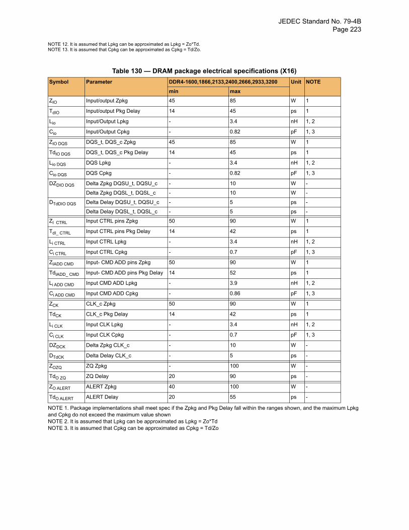
JEDEC Standard No. 79-4B Page 223
NOTE 12. It is assumed that Lpkg can be approximated as Lpkg = Zo*Td.NOTE 13. It is assumed that Cpkg can be approximated as Cpkg = Td/Zo.
Table 130 — DRAM package electrical specifications (X16)
NOTE 1. Package implementations shall meet spec if the Zpkg and Pkg Delay fall within the ranges shown, and the maximum Lpkg and Cpkg do not exceed the maximum value shownNOTE 2. It is assumed that Lpkg can be approximated as Lpkg = Zo*TdNOTE 3. It is assumed that Cpkg can be approximated as Cpkg = Td/Zo
Symbol Parameter DDR4-1600,1866,2133,2400,2666,2933,3200 Unit NOTE
min max
ZIO Input/output Zpkg 45 85 W 1
TdIO Input/output Pkg Delay 14 45 ps 1
Lio Input/Output Lpkg - 3.4 nH 1, 2
Cio Input/Output Cpkg - 0.82 pF 1, 3
ZIO DQS DQS_t, DQS_c Zpkg 45 85 W 1
TdIO DQS DQS_t, DQS_c Pkg Delay 14 45 ps 1
Lio DQS DQS Lpkg - 3.4 nH 1, 2
Cio DQS DQS Cpkg - 0.82 pF 1, 3
DZDIO DQS Delta Zpkg DQSU_t, DQSU_c - 10 W -
Delta Zpkg DQSL_t, DQSL_c - 10 W -
DTdDIO DQS Delta Delay DQSU_t, DQSU_c - 5 ps -
Delta Delay DQSL_t, DQSL_c - 5 ps -
ZI CTRL Input CTRL pins Zpkg 50 90 W 1
TdI_ CTRL Input CTRL pins Pkg Delay 14 42 ps 1
Li CTRL Input CTRL Lpkg - 3.4 nH 1, 2
Ci CTRL Input CTRL Cpkg - 0.7 pF 1, 3
ZIADD CMD Input- CMD ADD pins Zpkg 50 90 W 1
TdIADD_ CMD Input- CMD ADD pins Pkg Delay 14 52 ps 1
Li ADD CMD Input CMD ADD Lpkg - 3.9 nH 1, 2
Ci ADD CMD Input CMD ADD Cpkg - 0.86 pF 1, 3
ZCK CLK_c Zpkg 50 90 W 1
TdCK CLK_c Pkg Delay 14 42 ps 1
Li CLK Input CLK Lpkg - 3.4 nH 1, 2
Ci CLK Input CLK Cpkg - 0.7 pF 1, 3
DZDCK Delta Zpkg CLK_c - 10 W -
DTdCK Delta Delay CLK_c - 5 ps -
ZOZQ ZQ Zpkg - 100 W -
TdO ZQ ZQ Delay 20 90 ps -
ZO ALERT ALERT Zpkg 40 100 W -
TdO ALERT ALERT Delay 20 55 ps -
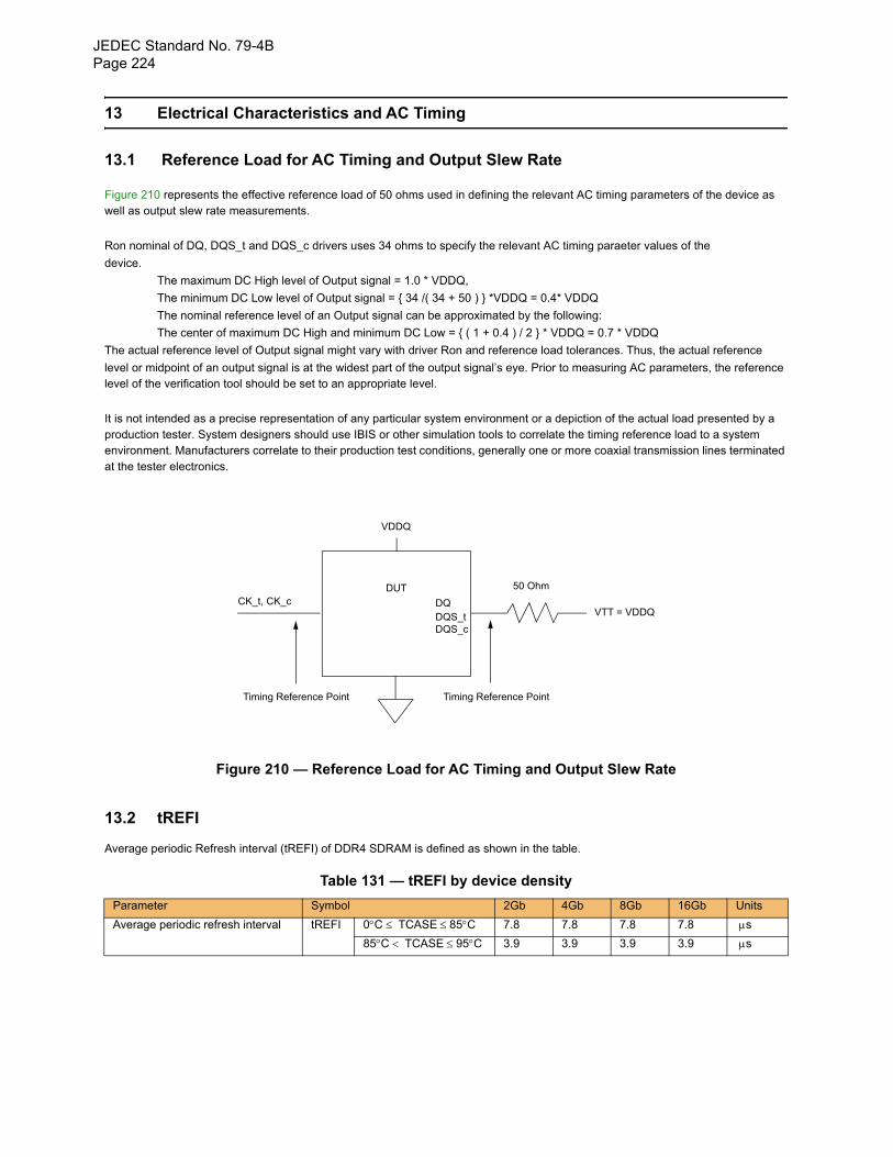
JEDEC Standard No. 79-4BPage 224
13 Electrical Characteristics and AC Timing
13.1 Reference Load for AC Timing and Output Slew Rate
Figure 210 represents the effective reference load of 50 ohms used in defining the relevant AC timing parameters of the device as well as output slew rate measurements.
Ron nominal of DQ, DQS_t and DQS_c drivers uses 34 ohms to specify the relevant AC timing paraeter values of the
device.
The maximum DC High level of Output signal = 1.0 * VDDQ,
The minimum DC Low level of Output signal = { 34 /( 34 + 50 ) } *VDDQ = 0.4* VDDQ
The nominal reference level of an Output signal can be approximated by the following:
The center of maximum DC High and minimum DC Low = { ( 1 + 0.4 ) / 2 } * VDDQ = 0.7 * VDDQ
The actual reference level of Output signal might vary with driver Ron and reference load tolerances. Thus, the actual reference
level or midpoint of an output signal is at the widest part of the output signal’s eye. Prior to measuring AC parameters, the reference level of the verification tool should be set to an appropriate level.
It is not intended as a precise representation of any particular system environment or a depiction of the actual load presented by a production tester. System designers should use IBIS or other simulation tools to correlate the timing reference load to a system environment. Manufacturers correlate to their production test conditions, generally one or more coaxial transmission lines terminated at the tester electronics.
Figure 210 — Reference Load for AC Timing and Output Slew Rate
13.2 tREFI
Average periodic Refresh interval (tREFI) of DDR4 SDRAM is defined as shown in the table.
Table 131 — tREFI by device density
Parameter Symbol 2Gb 4Gb 8Gb 16Gb Units
Average periodic refresh interval tREFI 0C TCASE85C 7.8 7.8 7.8 7.8 s
85C TCASE95C 3.9 3.9 3.9 3.9 s
VDDQ
CK_t, CK_c
Timing Reference Point
DUT
DQDQS_tDQS_c
Timing Reference Point
VTT = VDDQ
50 Ohm
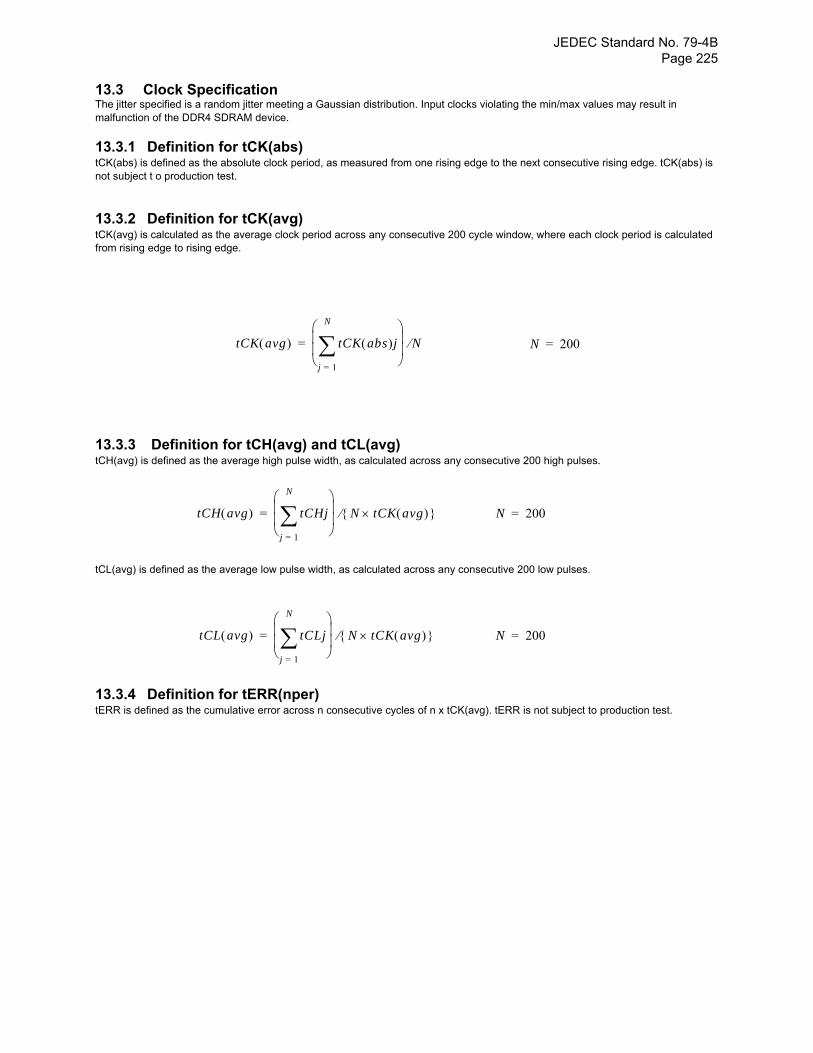
JEDEC Standard No. 79-4B Page 225
13.3 Clock SpecificationThe jitter specified is a random jitter meeting a Gaussian distribution. Input clocks violating the min/max values may result in malfunction of the DDR4 SDRAM device.
13.3.1 Definition for tCK(abs)tCK(abs) is defined as the absolute clock period, as measured from one rising edge to the next consecutive rising edge. tCK(abs) is not subject t o production test.
13.3.2 Definition for tCK(avg)tCK(avg) is calculated as the average clock period across any consecutive 200 cycle window, where each clock period is calculated from rising edge to rising edge.
13.3.3 Definition for tCH(avg) and tCL(avg)tCH(avg) is defined as the average high pulse width, as calculated across any consecutive 200 high pulses.
tCL(avg) is defined as the average low pulse width, as calculated across any consecutive 200 low pulses.
13.3.4 Definition for tERR(nper)tERR is defined as the cumulative error across n consecutive cycles of n x tCK(avg). tERR is not subject to production test.
tCK avg tCK abs j
j 1=
N
N= N 200=
tCH avg tCHj
j 1=
N
N tCK avg = N 200=
tCL avg tCLj
j 1=
N
N tCK avg = N 200=
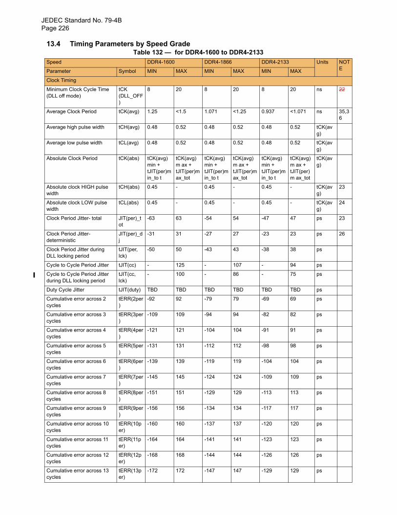
JEDEC Standard No. 79-4BPage 226
13.4 Timing Parameters by Speed GradeTable 132 — for DDR4-1600 to DDR4-2133
Speed DDR4-1600 DDR4-1866 DDR4-2133 Units NOTEParameter Symbol MIN MAX MIN MAX MIN MAX
Clock Timing
Minimum Clock Cycle Time (DLL off mode)
tCK (DLL_OFF)
8 20 8 20 8 20 ns 22
Average Clock Period tCK(avg) 1.25 <1.5 1.071 <1.25 0.937 <1.071 ns 35,36
Average high pulse width tCH(avg) 0.48 0.52 0.48 0.52 0.48 0.52 tCK(avg)
Average low pulse width tCL(avg) 0.48 0.52 0.48 0.52 0.48 0.52 tCK(avg)
Absolute Clock Period tCK(abs) tCK(avg)min + tJIT(per)min_to t
tCK(avg)m ax + tJIT(per)m ax_tot
tCK(avg)min + tJIT(per)min_to t
tCK(avg)m ax + tJIT(per)m ax_tot
tCK(avg)min + tJIT(per)min_to t
tCK(avg)m ax + tJIT(per)m ax_tot
tCK(avg)
Absolute clock HIGH pulse width
tCH(abs) 0.45 - 0.45 - 0.45 - tCK(avg)
23
Absolute clock LOW pulse width
tCL(abs) 0.45 - 0.45 - 0.45 - tCK(avg)
24
Clock Period Jitter- total JIT(per)_tot
-63 63 -54 54 -47 47 ps 23
Clock Period Jitter- deterministic
JIT(per)_dj
-31 31 -27 27 -23 23 ps 26
Clock Period Jitter during DLL locking period
tJIT(per, lck)
-50 50 -43 43 -38 38 ps
Cycle to Cycle Period Jitter tJIT(cc) - 125 - 107 - 94 ps
Cycle to Cycle Period Jitter during DLL locking period
tJIT(cc, lck)
- 100 - 86 - 75 ps
Duty Cycle Jitter tJIT(duty) TBD TBD TBD TBD TBD TBD ps
Cumulative error across 2 cycles
tERR(2per)
-92 92 -79 79 -69 69 ps
Cumulative error across 3 cycles
tERR(3per)
-109 109 -94 94 -82 82 ps
Cumulative error across 4 cycles
tERR(4per)
-121 121 -104 104 -91 91 ps
Cumulative error across 5 cycles
tERR(5per)
-131 131 -112 112 -98 98 ps
Cumulative error across 6 cycles
tERR(6per)
-139 139 -119 119 -104 104 ps
Cumulative error across 7 cycles
tERR(7per)
-145 145 -124 124 -109 109 ps
Cumulative error across 8 cycles
tERR(8per)
-151 151 -129 129 -113 113 ps
Cumulative error across 9 cycles
tERR(9per)
-156 156 -134 134 -117 117 ps
Cumulative error across 10 cycles
tERR(10per)
-160 160 -137 137 -120 120 ps
Cumulative error across 11 cycles
tERR(11per)
-164 164 -141 141 -123 123 ps
Cumulative error across 12 cycles
tERR(12per)
-168 168 -144 144 -126 126 ps
Cumulative error across 13 cycles
tERR(13per)
-172 172 -147 147 -129 129 ps
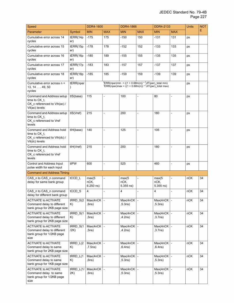
JEDEC Standard No. 79-4B Page 227
Cumulative error across 14 cycles
tERR(14per)
-175 175 -150 150 -131 131 ps
Cumulative error across 15 cycles
tERR(15per)
-178 178 -152 152 -133 133 ps
Cumulative error across 16 cycles
tERR(16per)
-180 189 -155 155 -135 135 ps
Cumulative error across 17 cycles
tERR(17per)
-183 183 -157 157 -137 137 ps
Cumulative error across 18 cycles
tERR(18per)
-185 185 -159 159 -139 139 ps
Cumulative error across n = 13, 14 . . . 49, 50 cycles
tERR(nper)
tERR(nper)min = ((1 + 0.68ln(n)) * tJIT(per)_total min) tERR(nper)max = ((1 + 0.68ln(n)) * tJIT(per)_total max)
ps
Command and Address setup time to CK_t,CK_c referenced to Vih(ac) / Vil(ac) levels
tIS(base) 115 - 100 - 80 - ps
Command and Address setup time to CK_t,CK_c referenced to Vref levels
tIS(Vref) 215 - 200 - 180 - ps
Command and Address hold time to CK_t,CK_c referenced to Vih(dc) / Vil(dc) levels
tIH(base) 140 - 125 - 105 - ps
Command and Address hold time to CK_t,CK_c referenced to Vref levels
tIH(Vref) 215 - 200 - 180 - ps
Control and Address Input pulse width for each input
tIPW 600 - 525 - 460 - ps
Command and Address Timing
CAS_n to CAS_n command delay for same bank group
tCCD_L max(5 nCK,6.250 ns)
- max(5 nCK,5.355 ns)
- max(5 nCK,5.355 ns)
- nCK 34
CAS_n to CAS_n command delay for different bank group
tCCD_S 4 - 4 - 4 - nCK 34
ACTIVATE to ACTIVATE Command delay to different bank group for 2KB page size
tRRD_S(2K)
Max(4nCK,6ns)
- Max(4nCK,5.3ns)
- Max(4nCK,5.3ns)
- nCK 34
ACTIVATE to ACTIVATE Command delay to different bank group for 2KB page size
tRRD_S(1K)
Max(4nCK,5ns)
- Max(4nCK,4.2ns)
- Max(4nCK,3.7ns)
- nCK 34
ACTIVATE to ACTIVATE Command delay to different bank group for 1/2KB page size
tRRD_S(1/2K)
Max(4nCK,5ns)
- Max(4nCK,4.2ns)
- Max(4nCK,3.7ns)
- nCK 34
ACTIVATE to ACTIVATE Command delay to same bank group for 2KB page size
tRRD_L(2K)
Max(4nCK,7.5ns)
- Max(4nCK,6.4ns)
- Max(4nCK,6.4ns)
- nCK 34
ACTIVATE to ACTIVATE Command delay to same bank group for 1KB page size
tRRD_L(1K)
Max(4nCK,6ns)
- Max(4nCK,5.3ns)
- Max(4nCK,5.3ns)
- nCK 34
ACTIVATE to ACTIVATE Command delay to same bank group for 1/2KB page size
tRRD_L(1/2K)
Max(4nCK,6ns)
- Max(4nCK,5.3ns)
- Max(4nCK,5.3ns)
- nCK 34
Speed DDR4-1600 DDR4-1866 DDR4-2133 Units NOTEParameter Symbol MIN MAX MIN MAX MIN MAX
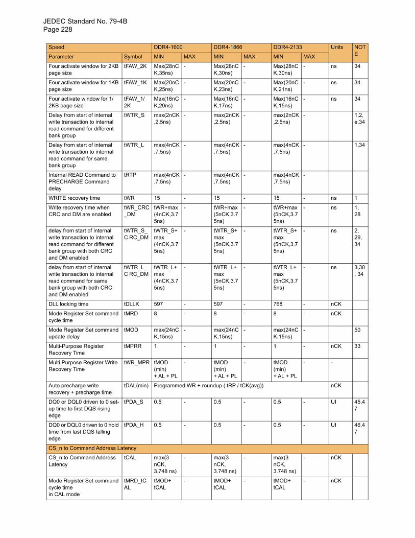
JEDEC Standard No. 79-4BPage 228
Four activate window for 2KB page size
tFAW_2K Max(28nCK,35ns)
- Max(28nCK,30ns)
- Max(28nCK,30ns)
- ns 34
Four activate window for 1KB page size
tFAW_1K Max(20nCK,25ns)
- Max(20nCK,23ns)
- Max(20nCK,21ns)
- ns 34
Four activate window for 1/2KB page size
tFAW_1/2K
Max(16nCK,20ns)
- Max(16nCK,17ns)
- Max(16nCK,15ns)
- ns 34
Delay from start of internal write transaction to internal read command for different bank group
tWTR_S max(2nCK,2.5ns)
- max(2nCK,2.5ns)
- max(2nCK,2.5ns)
- 1,2,e,34
Delay from start of internal write transaction to internal read command for same bank group
tWTR_L max(4nCK,7.5ns)
- max(4nCK,7.5ns)
- max(4nCK,7.5ns)
- 1,34
Internal READ Command to PRECHARGE Command delay
tRTP max(4nCK,7.5ns)
- max(4nCK,7.5ns)
- max(4nCK,7.5ns)
-
WRITE recovery time tWR 15 - 15 - 15 - ns 1
Write recovery time when CRC and DM are enabled
tWR_CRC _DM
tWR+max(4nCK,3.75ns)
- tWR+max(5nCK,3.75ns)
- tWR+max(5nCK,3.75ns)
- ns 1, 28
delay from start of internal write transaction to internal read command for different bank group with both CRC and DM enabled
tWTR_S_C RC_DM
tWTR_S+max(4nCK,3.75ns)
- tWTR_S+max(5nCK,3.75ns)
- tWTR_S+max(5nCK,3.75ns)
- ns 2, 29, 34
delay from start of internal write transaction to internal read command for same bank group with both CRC and DM enabled
tWTR_L_C RC_DM
tWTR_L+max(4nCK,3.75ns)
- tWTR_L+max(5nCK,3.75ns)
- tWTR_L+max(5nCK,3.75ns)
- ns 3,30, 34
DLL locking time tDLLK 597 - 597 - 768 - nCK
Mode Register Set command cycle time
tMRD 8 - 8 - 8 - nCK
Mode Register Set command update delay
tMOD max(24nCK,15ns)
- max(24nCK,15ns)
- max(24nCK,15ns)
- 50
Multi-Purpose Register Recovery Time
tMPRR 1 - 1 - 1 - nCK 33
Multi Purpose Register Write Recovery Time
tWR_MPR tMOD (min) + AL + PL
- tMOD (min) + AL + PL
- tMOD (min) + AL + PL
- -
Auto precharge write recovery + precharge time
tDAL(min) Programmed WR + roundup ( tRP / tCK(avg)) nCK
DQ0 or DQL0 driven to 0 set-up time to first DQS rising edge
tPDA_S 0.5 - 0.5 - 0.5 - UI 45,47
DQ0 or DQL0 driven to 0 hold time from last DQS falling edge
tPDA_H 0.5 - 0.5 - 0.5 - UI 46,47
CS_n to Command Address Latency
CS_n to Command Address Latency
tCAL max(3 nCK,3.748 ns)
- max(3 nCK,3.748 ns)
- max(3 nCK,3.748 ns)
- nCK
Mode Register Set command cycle timein CAL mode
tMRD_tCAL
tMOD+tCAL
- tMOD+tCAL
- tMOD+tCAL
- nCK
Speed DDR4-1600 DDR4-1866 DDR4-2133 Units NOTEParameter Symbol MIN MAX MIN MAX MIN MAX
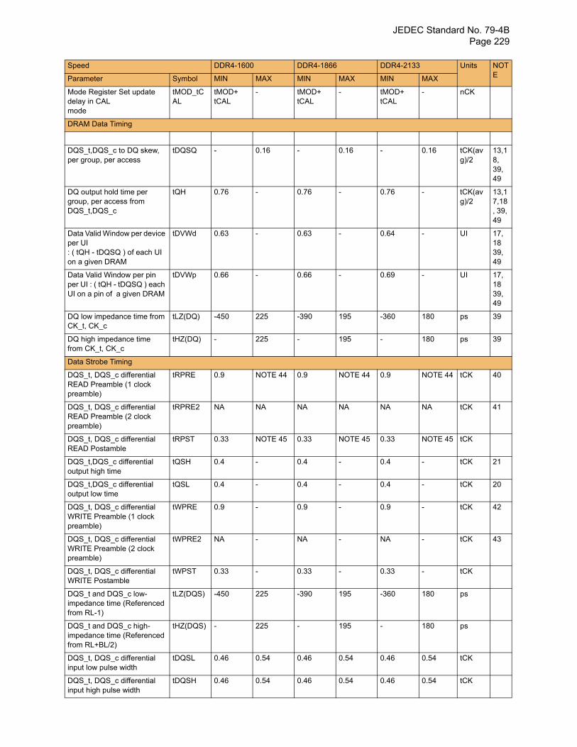
JEDEC Standard No. 79-4B Page 229
Mode Register Set update delay in CALmode
tMOD_tCAL
tMOD+tCAL
- tMOD+tCAL
- tMOD+tCAL
- nCK
DRAM Data Timing
DQS_t,DQS_c to DQ skew, per group, per access
tDQSQ - 0.16 - 0.16 - 0.16 tCK(avg)/2
13,18, 39, 49
DQ output hold time per group, per access from DQS_t,DQS_c
tQH 0.76 - 0.76 - 0.76 - tCK(avg)/2
13,17,18, 39, 49
Data Valid Window per device per UI: ( tQH - tDQSQ ) of each UI on a given DRAM
tDVWd 0.63 - 0.63 - 0.64 - UI 17, 1839, 49
Data Valid Window per pin per UI : ( tQH - tDQSQ ) each UI on a pin of a given DRAM
tDVWp 0.66 - 0.66 - 0.69 - UI 17, 1839, 49
DQ low impedance time from CK_t, CK_c
tLZ(DQ) -450 225 -390 195 -360 180 ps 39
DQ high impedance time from CK_t, CK_c
tHZ(DQ) - 225 - 195 - 180 ps 39
Data Strobe Timing
DQS_t, DQS_c differential READ Preamble (1 clock preamble)
tRPRE 0.9 NOTE 44 0.9 NOTE 44 0.9 NOTE 44 tCK 40
DQS_t, DQS_c differential READ Preamble (2 clock preamble)
tRPRE2 NA NA NA NA NA NA tCK 41
DQS_t, DQS_c differential READ Postamble
tRPST 0.33 NOTE 45 0.33 NOTE 45 0.33 NOTE 45 tCK
DQS_t,DQS_c differential output high time
tQSH 0.4 - 0.4 - 0.4 - tCK 21
DQS_t,DQS_c differential output low time
tQSL 0.4 - 0.4 - 0.4 - tCK 20
DQS_t, DQS_c differential WRITE Preamble (1 clock preamble)
tWPRE 0.9 - 0.9 - 0.9 - tCK 42
DQS_t, DQS_c differential WRITE Preamble (2 clock preamble)
tWPRE2 NA - NA - NA - tCK 43
DQS_t, DQS_c differential WRITE Postamble
tWPST 0.33 - 0.33 - 0.33 - tCK
DQS_t and DQS_c low-impedance time (Referenced from RL-1)
tLZ(DQS) -450 225 -390 195 -360 180 ps
DQS_t and DQS_c high-impedance time (Referenced from RL+BL/2)
tHZ(DQS) - 225 - 195 - 180 ps
DQS_t, DQS_c differential input low pulse width
tDQSL 0.46 0.54 0.46 0.54 0.46 0.54 tCK
DQS_t, DQS_c differential input high pulse width
tDQSH 0.46 0.54 0.46 0.54 0.46 0.54 tCK
Speed DDR4-1600 DDR4-1866 DDR4-2133 Units NOTEParameter Symbol MIN MAX MIN MAX MIN MAX
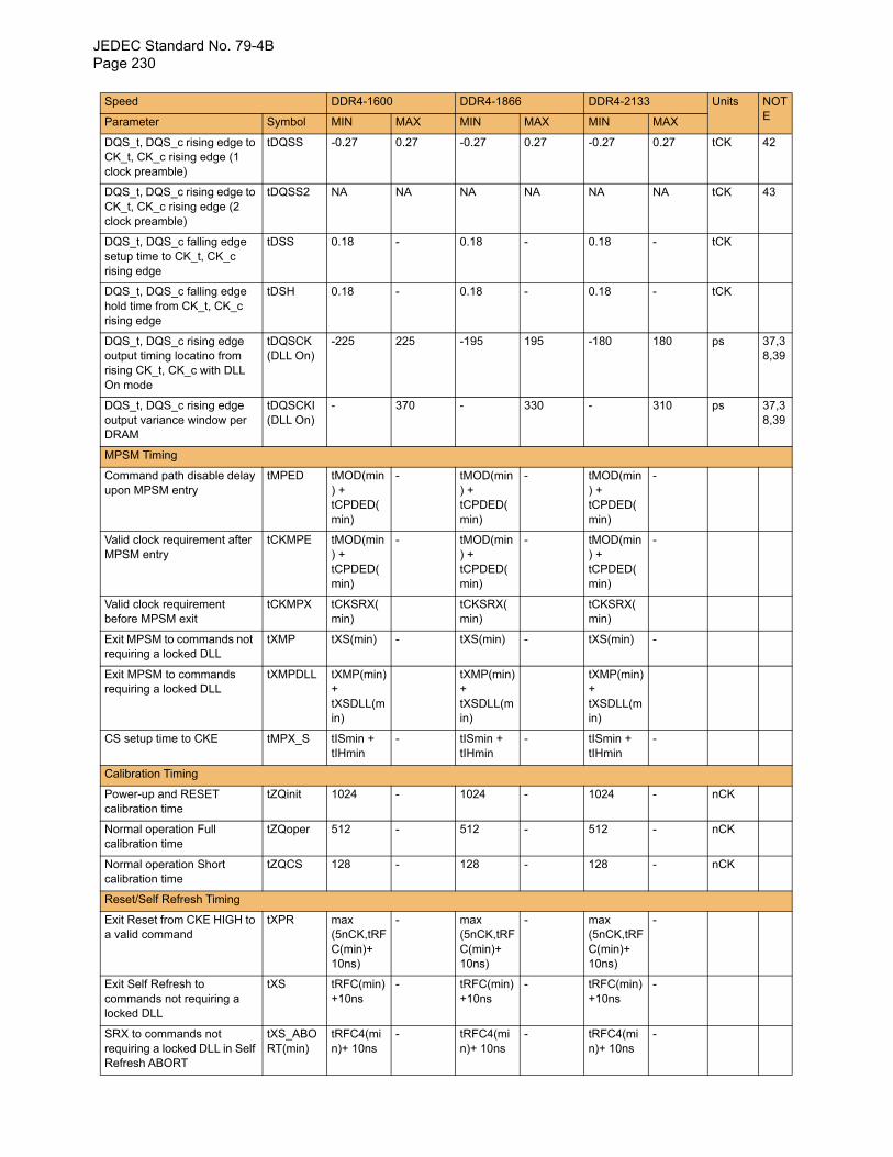
JEDEC Standard No. 79-4BPage 230
DQS_t, DQS_c rising edge to CK_t, CK_c rising edge (1 clock preamble)
tDQSS -0.27 0.27 -0.27 0.27 -0.27 0.27 tCK 42
DQS_t, DQS_c rising edge to CK_t, CK_c rising edge (2 clock preamble)
tDQSS2 NA NA NA NA NA NA tCK 43
DQS_t, DQS_c falling edge setup time to CK_t, CK_c rising edge
tDSS 0.18 - 0.18 - 0.18 - tCK
DQS_t, DQS_c falling edge hold time from CK_t, CK_c rising edge
tDSH 0.18 - 0.18 - 0.18 - tCK
DQS_t, DQS_c rising edge output timing locatino from rising CK_t, CK_c with DLL On mode
tDQSCK(DLL On)
-225 225 -195 195 -180 180 ps 37,38,39
DQS_t, DQS_c rising edge output variance window per DRAM
tDQSCKI(DLL On)
- 370 - 330 - 310 ps 37,38,39
MPSM Timing
Command path disable delay upon MPSM entry
tMPED tMOD(min) + tCPDED(min)
- tMOD(min) + tCPDED(min)
- tMOD(min) + tCPDED(min)
-
Valid clock requirement after MPSM entry
tCKMPE tMOD(min) +tCPDED(min)
- tMOD(min) + tCPDED(min)
- tMOD(min) + tCPDED(min)
-
Valid clock requirement before MPSM exit
tCKMPX tCKSRX(min)
tCKSRX(min)
tCKSRX(min)
Exit MPSM to commands not requiring a locked DLL
tXMP tXS(min) - tXS(min) - tXS(min) -
Exit MPSM to commands requiring a locked DLL
tXMPDLL tXMP(min) + tXSDLL(min)
tXMP(min) + tXSDLL(min)
tXMP(min) +tXSDLL(min)
CS setup time to CKE tMPX_S tISmin + tIHmin
- tISmin + tIHmin
- tISmin + tIHmin
-
Calibration Timing
Power-up and RESET calibration time
tZQinit 1024 - 1024 - 1024 - nCK
Normal operation Full calibration time
tZQoper 512 - 512 - 512 - nCK
Normal operation Short calibration time
tZQCS 128 - 128 - 128 - nCK
Reset/Self Refresh Timing
Exit Reset from CKE HIGH to a valid command
tXPR max(5nCK,tRFC(min)+10ns)
- max(5nCK,tRFC(min)+10ns)
- max(5nCK,tRFC(min)+10ns)
-
Exit Self Refresh to commands not requiring a locked DLL
tXS tRFC(min)+10ns
- tRFC(min)+10ns
- tRFC(min)+10ns
-
SRX to commands not requiring a locked DLL in Self Refresh ABORT
tXS_ABORT(min)
tRFC4(min)+ 10ns
- tRFC4(min)+ 10ns
- tRFC4(min)+ 10ns
-
Speed DDR4-1600 DDR4-1866 DDR4-2133 Units NOTEParameter Symbol MIN MAX MIN MAX MIN MAX
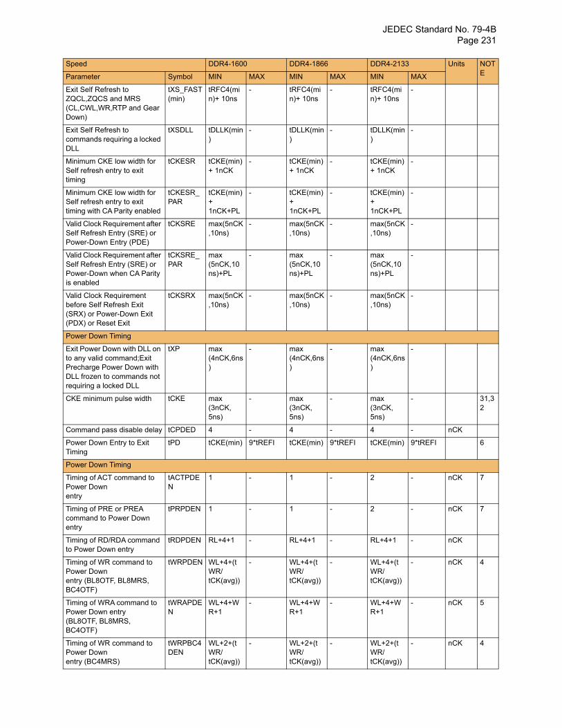
JEDEC Standard No. 79-4B Page 231
Exit Self Refresh to ZQCL,ZQCS and MRS (CL,CWL,WR,RTP and Gear Down)
tXS_FAST (min)
tRFC4(min)+ 10ns
- tRFC4(min)+ 10ns
- tRFC4(min)+ 10ns
-
Exit Self Refresh to commands requiring a locked DLL
tXSDLL tDLLK(min)
- tDLLK(min)
- tDLLK(min)
-
Minimum CKE low width for Self refresh entry to exit timing
tCKESR tCKE(min)+ 1nCK
- tCKE(min)+ 1nCK
- tCKE(min)+ 1nCK
-
Minimum CKE low width for Self refresh entry to exit timing with CA Parity enabled
tCKESR_ PAR
tCKE(min)+ 1nCK+PL
- tCKE(min)+ 1nCK+PL
- tCKE(min)+ 1nCK+PL
-
Valid Clock Requirement after Self Refresh Entry (SRE) or Power-Down Entry (PDE)
tCKSRE max(5nCK,10ns)
- max(5nCK,10ns)
- max(5nCK,10ns)
-
Valid Clock Requirement after Self Refresh Entry (SRE) or Power-Down when CA Parity is enabled
tCKSRE_PAR
max(5nCK,10ns)+PL
- max(5nCK,10ns)+PL
- max(5nCK,10ns)+PL
-
Valid Clock Requirement before Self Refresh Exit (SRX) or Power-Down Exit (PDX) or Reset Exit
tCKSRX max(5nCK,10ns)
- max(5nCK,10ns)
- max(5nCK,10ns)
-
Power Down Timing
Exit Power Down with DLL on to any valid command;Exit Precharge Power Down with DLL frozen to commands not requiring a locked DLL
tXP max (4nCK,6ns)
- max (4nCK,6ns)
- max (4nCK,6ns)
-
CKE minimum pulse width tCKE max (3nCK, 5ns)
- max (3nCK, 5ns)
- max (3nCK, 5ns)
- 31,32
Command pass disable delay tCPDED 4 - 4 - 4 - nCK
Power Down Entry to Exit Timing
tPD tCKE(min) 9*tREFI tCKE(min) 9*tREFI tCKE(min) 9*tREFI 6
Power Down Timing
Timing of ACT command to Power Down entry
tACTPDEN
1 - 1 - 2 - nCK 7
Timing of PRE or PREA command to Power Down entry
tPRPDEN 1 - 1 - 2 - nCK 7
Timing of RD/RDA command to Power Down entry
tRDPDEN RL+4+1 - RL+4+1 - RL+4+1 - nCK
Timing of WR command to Power Down entry (BL8OTF, BL8MRS, BC4OTF)
tWRPDEN WL+4+(tWR/tCK(avg))
- WL+4+(tWR/tCK(avg))
- WL+4+(tWR/tCK(avg))
- nCK 4
Timing of WRA command to Power Down entry(BL8OTF, BL8MRS, BC4OTF)
tWRAPDEN
WL+4+WR+1
- WL+4+WR+1
- WL+4+WR+1
- nCK 5
Timing of WR command to Power Down entry (BC4MRS)
tWRPBC4DEN
WL+2+(tWR/tCK(avg))
- WL+2+(tWR/tCK(avg))
- WL+2+(tWR/tCK(avg))
- nCK 4
Speed DDR4-1600 DDR4-1866 DDR4-2133 Units NOTEParameter Symbol MIN MAX MIN MAX MIN MAX
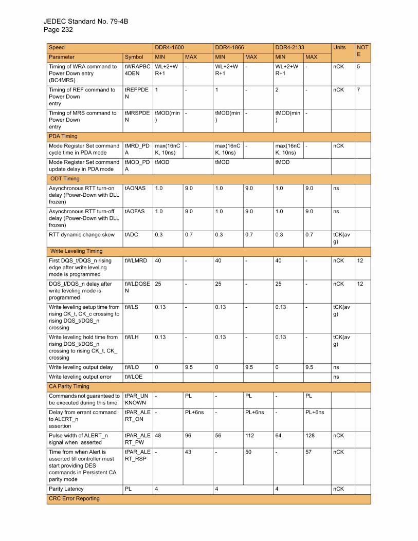
JEDEC Standard No. 79-4BPage 232
Timing of WRA command to Power Down entry (BC4MRS)
tWRAPBC4DEN
WL+2+WR+1
- WL+2+WR+1
- WL+2+WR+1
- nCK 5
Timing of REF command to Power Down entry
tREFPDEN
1 - 1 - 2 - nCK 7
Timing of MRS command to Power Down entry
tMRSPDEN
tMOD(min)
- tMOD(min)
- tMOD(min)
-
PDA Timing
Mode Register Set command cycle time in PDA mode
tMRD_PDA
max(16nCK, 10ns)
- max(16nCK, 10ns)
- max(16nCK, 10ns)
- nCK
Mode Register Set command update delay in PDA mode
tMOD_PDA
tMOD tMOD tMOD
ODT Timing
Asynchronous RTT turn-on delay (Power-Down with DLL frozen)
tAONAS 1.0 9.0 1.0 9.0 1.0 9.0 ns
Asynchronous RTT turn-off delay (Power-Down with DLL frozen)
tAOFAS 1.0 9.0 1.0 9.0 1.0 9.0 ns
RTT dynamic change skew tADC 0.3 0.7 0.3 0.7 0.3 0.7 tCK(avg)
Write Leveling Timing
First DQS_t/DQS_n rising edge after write leveling mode is programmed
tWLMRD 40 - 40 - 40 - nCK 12
DQS_t/DQS_n delay after write leveling mode is programmed
tWLDQSEN
25 - 25 - 25 - nCK 12
Write leveling setup time from rising CK_t, CK_c crossing to rising DQS_t/DQS_n crossing
tWLS 0.13 - 0.13 - 0.13 - tCK(avg)
Write leveling hold time from rising DQS_t/DQS_n crossing to rising CK_t, CK_ crossing
tWLH 0.13 - 0.13 - 0.13 - tCK(avg)
Write leveling output delay tWLO 0 9.5 0 9.5 0 9.5 ns
Write leveling output error tWLOE ns
CA Parity Timing
Commands not guaranteed to be executed during this time
tPAR_UNKNOWN
- PL - PL - PL
Delay from errant command to ALERT_n assertion
tPAR_ALERT_ON
- PL+6ns - PL+6ns - PL+6ns
Pulse width of ALERT_n signal when asserted
tPAR_ALERT_PW
48 96 56 112 64 128 nCK
Time from when Alert is asserted till controller must start providing DES commands in Persistent CA parity mode
tPAR_ALERT_RSP
- 43 - 50 - 57 nCK
Parity Latency PL 4 4 4 nCK
CRC Error Reporting
Speed DDR4-1600 DDR4-1866 DDR4-2133 Units NOTEParameter Symbol MIN MAX MIN MAX MIN MAX
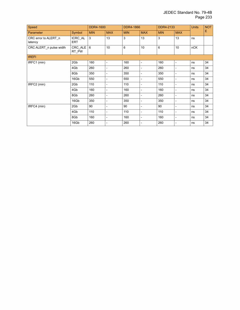
JEDEC Standard No. 79-4B Page 233
CRC error to ALERT_n latency
tCRC_ALERT
3 13 3 13 3 13 ns
CRC ALERT_n pulse width CRC_ALERT_PW
6 10 6 10 6 10 nCK
tREFI
tRFC1 (min) 2Gb 160 - 160 - 160 - ns 34
4Gb 260 - 260 - 260 - ns 34
8Gb 350 - 350 - 350 - ns 34
16Gb 550 - 550 - 550 - ns 34
tRFC2 (min) 2Gb 110 - 110 - 110 - ns 34
4Gb 160 - 160 - 160 - ns 34
8Gb 260 - 260 - 260 - ns 34
16Gb 350 - 350 - 350 - ns 34
tRFC4 (min) 2Gb 90 - 90 - 90 - ns 34
4Gb 110 - 110 - 110 - ns 34
8Gb 160 - 160 - 160 - ns 34
16Gb 260 - 260 - 260 - ns 34
Speed DDR4-1600 DDR4-1866 DDR4-2133 Units NOTEParameter Symbol MIN MAX MIN MAX MIN MAX
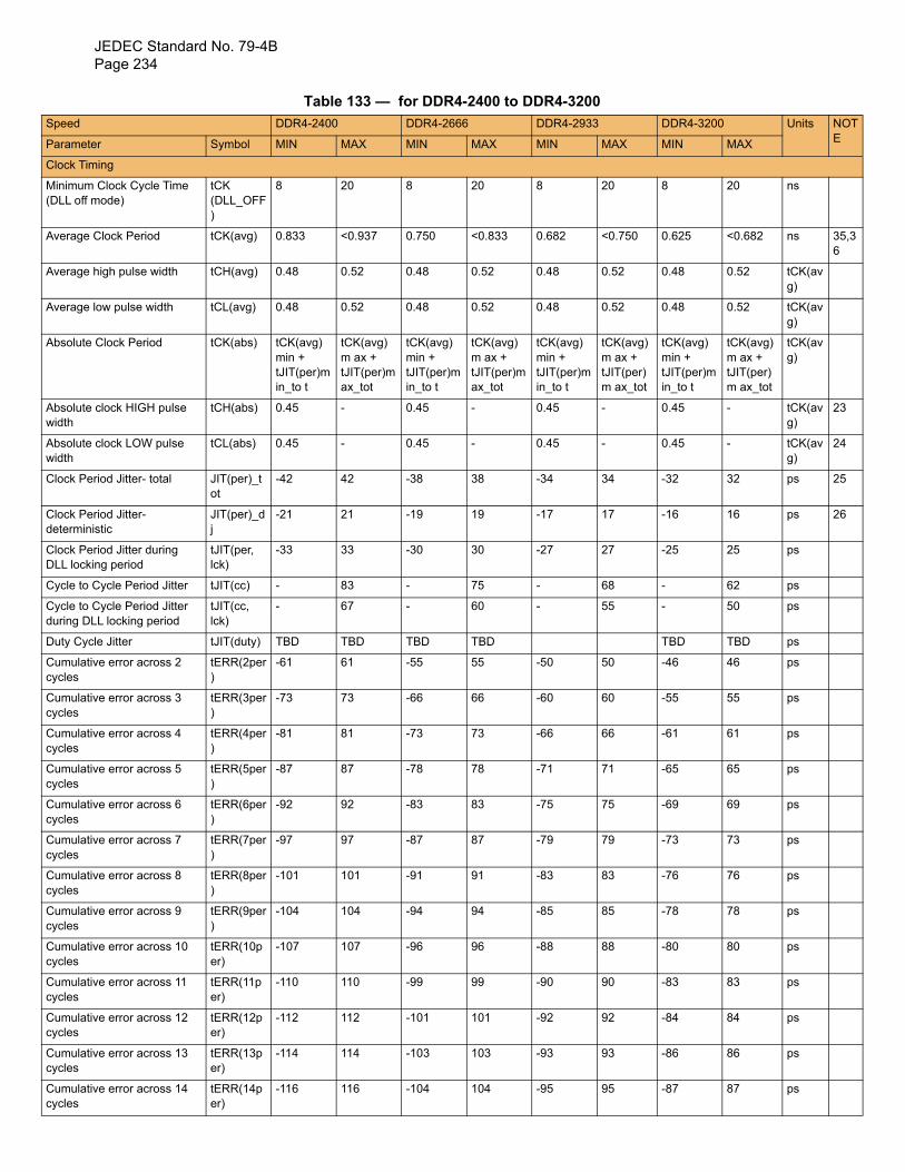
JEDEC Standard No. 79-4BPage 234
Speed NOTEParamete
Clock Tim
Minimum(DLL off m
Average C 35,36
Average h v
Average l v
Absolute v
Absolute width
v 23
Absolute width
v 24
Clock Per 25
Clock Pedetermini
26
Clock PerDLL locki
Cycle to C
Cycle to Cduring DL
Duty Cyc
Cumulativcycles
Cumulativcycles
Cumulativcycles
Cumulativcycles
Cumulativcycles
Cumulativcycles
Cumulativcycles
Cumulativcycles
Cumulativcycles
Cumulativcycles
Cumulativcycles
Cumulativcycles
Cumulativcycles
Table 133 — for DDR4-2400 to DDR4-3200
DDR4-2400 DDR4-2666 DDR4-2933 DDR4-3200 Units
r Symbol MIN MAX MIN MAX MIN MAX MIN MAX
ing
Clock Cycle Time ode)
tCK (DLL_OFF)
8 20 8 20 8 20 8 20 ns
lock Period tCK(avg) 0.833 <0.937 0.750 <0.833 0.682 <0.750 0.625 <0.682 ns
igh pulse width tCH(avg) 0.48 0.52 0.48 0.52 0.48 0.52 0.48 0.52 tCK(ag)
ow pulse width tCL(avg) 0.48 0.52 0.48 0.52 0.48 0.52 0.48 0.52 tCK(ag)
Clock Period tCK(abs) tCK(avg)min + tJIT(per)min_to t
tCK(avg)m ax + tJIT(per)m ax_tot
tCK(avg)min + tJIT(per)min_to t
tCK(avg)m ax + tJIT(per)m ax_tot
tCK(avg)min + tJIT(per)min_to t
tCK(avg)m ax + tJIT(per)m ax_tot
tCK(avg)min + tJIT(per)min_to t
tCK(avg)m ax + tJIT(per)m ax_tot
tCK(ag)
clock HIGH pulse tCH(abs) 0.45 - 0.45 - 0.45 - 0.45 - tCK(ag)
clock LOW pulse tCL(abs) 0.45 - 0.45 - 0.45 - 0.45 - tCK(ag)
iod Jitter- total JIT(per)_tot
-42 42 -38 38 -34 34 -32 32 ps
riod Jitter- stic
JIT(per)_dj
-21 21 -19 19 -17 17 -16 16 ps
iod Jitter during ng period
tJIT(per, lck)
-33 33 -30 30 -27 27 -25 25 ps
ycle Period Jitter tJIT(cc) - 83 - 75 - 68 - 62 ps
ycle Period Jitter L locking period
tJIT(cc, lck)
- 67 - 60 - 55 - 50 ps
le Jitter tJIT(duty) TBD TBD TBD TBD TBD TBD ps
e error across 2 tERR(2per)
-61 61 -55 55 -50 50 -46 46 ps
e error across 3 tERR(3per)
-73 73 -66 66 -60 60 -55 55 ps
e error across 4 tERR(4per)
-81 81 -73 73 -66 66 -61 61 ps
e error across 5 tERR(5per)
-87 87 -78 78 -71 71 -65 65 ps
e error across 6 tERR(6per)
-92 92 -83 83 -75 75 -69 69 ps
e error across 7 tERR(7per)
-97 97 -87 87 -79 79 -73 73 ps
e error across 8 tERR(8per)
-101 101 -91 91 -83 83 -76 76 ps
e error across 9 tERR(9per)
-104 104 -94 94 -85 85 -78 78 ps
e error across 10 tERR(10per)
-107 107 -96 96 -88 88 -80 80 ps
e error across 11 tERR(11per)
-110 110 -99 99 -90 90 -83 83 ps
e error across 12 tERR(12per)
-112 112 -101 101 -92 92 -84 84 ps
e error across 13 tERR(13per)
-114 114 -103 103 -93 93 -86 86 ps
e error across 14 tERR(14per)
-116 116 -104 104 -95 95 -87 87 ps
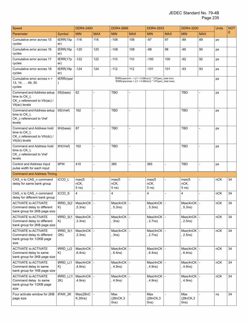
JEDEC Standard No. 79-4B Page 235
Cumulativcycles
Cumulativcycles
Cumulativcycles
Cumulativcycles
Cumulativ13, 14 . . cycles
Commantime to CCK_c refeVil(ac) lev
Commantime to CCK_c refelevels
Commantime to CCK_c refeVil(dc) lev
Commantime to CCK_c refelevels
Control apulse wid
Comman
CAS_n todelay for
34
CAS_n todelay for
34
ACTIVATCommanbank grou
34
ACTIVATCommanbank grou
34
ACTIVATCommanbank grousize
34
ACTIVATCommanbank grou
34
ACTIVATCommanbank grou
34
ACTIVATCommanbank grousize
34
Four activpage size
34
Speed NOTEParamete
e error across 15 tERR(15per)
-118 118 -106 106 -97 97 -89 89 ps
e error across 16 tERR(16per)
-120 120 -108 108 -98 98 -90 90 ps
e error across 17 tERR(17per)
-122 122 -110 110 -100 100 -92 92 ps
e error across 18 tERR(18per)
-124 124 -112 112 -101 101 -93 93 ps
e error across n = . 49, 50
tERR(nper)
tERR(nper)min = ((1 + 0.68ln(n)) * tJIT(per)_total min) tERR(nper)max = ((1 + 0.68ln(n)) * tJIT(per)_total max)
ps
d and Address setup K_t,renced to Vih(ac) / els
tIS(base) 62 - TBD - TBD - ps
d and Address setup K_t,renced to Vref
tIS(Vref) 162 - TBD - TBD - ps
d and Address hold K_t,renced to Vih(dc) / els
tIH(base) 87 - TBD - TBD - ps
d and Address hold K_t,renced to Vref
tIH(Vref) 162 - TBD - TBD - ps
nd Address Input th for each input
tIPW 410 - 385 - 365 - TBD - ps
d and Address Timing
CAS_n command same bank group
tCCD_L max(5 nCK,5 ns)
- max(5 nCK,5 ns)
- max(5 nCK,5 ns)
- max(5 nCK,5 ns)
- nCK
CAS_n command different bank group
tCCD_S 4 - 4 - 4 - 4 - nCK
E to ACTIVATE d delay to different p for 2KB page size
tRRD_S(2K)
Max(4nCK,5.3ns)
- Max(4nCK, 5.3ns)
- Max(4nCK, 5.3ns)
- Max(4nCK, 5.3ns)
- nCK
E to ACTIVATE d delay to different p for 2KB page size
tRRD_S(1K)
Max(4nCK,3.3ns)
- Max(4nCK, 3ns)
- Max(4nCK, 2.7ns)
- Max(4nCK, 2.5ns)
- nCK
E to ACTIVATE d delay to different p for 1/2KB page
tRRD_S(1/2K)
Max(4nCK,3.3ns)
- Max(4nCK, 3ns)
- Max(4nCK, 2.7ns)
- Max(4nCK, 2.5ns)
- nCK
E to ACTIVATE d delay to same p for 2KB page size
tRRD_L(2K)
Max(4nCK,6.4ns)
- Max(4nCK, 6.4ns)
- Max(4nCK, 6.4ns)
- Max(4nCK, 6.4ns)
- nCK
E to ACTIVATE d delay to same p for 1KB page size
tRRD_L(1K)
Max(4nCK,4.9ns)
- Max(4nCK, 4.9ns)
- Max(4nCK, 4.9ns)
- Max(4nCK, 4.9ns)
- nCK
E to ACTIVATE d delay to same p for 1/2KB page
tRRD_L(1/2K)
Max(4nCK,4.9ns)
- Max(4nCK, 4.9ns)
- Max(4nCK, 4.9ns)
- Max(4nCK, 4.9ns)
- nCK
ate window for 2KB tFAW_2K Max(28nCK,30ns)
- Max (28nCK,30ns)
- Max (28nCK,30ns)
- Max(28nCK,30ns)
- ns
DDR4-2400 DDR4-2666 DDR4-2933 DDR4-3200 Units
r Symbol MIN MAX MIN MAX MIN MAX MIN MAX
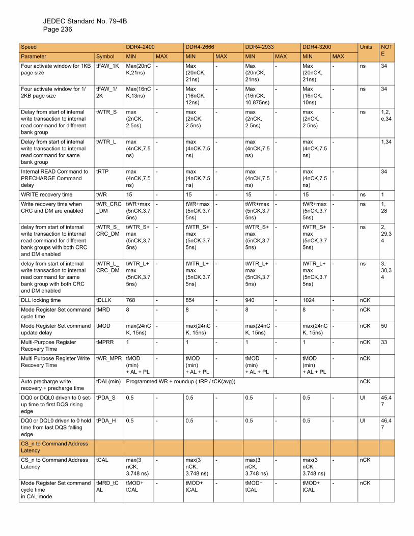
JEDEC Standard No. 79-4BPage 236
Four activpage size
34
Four activ2KB page
34
Delay fromwrite tranread combank grou
1,2,e,34
Delay fromwrite tranread combank grou
1,34
Internal RPRECHAdelay
34
WRITE re 1
Write recoCRC and
1, 28
delay fromwrite tranread combank grouand DM e
2, 29,34
delay fromwrite tranread combank grouand DM e
3, 30,34
DLL locki
Mode Recycle time
Mode Reupdate de
50
Multi-PurpRecovery
33
Multi PurpRecovery
Auto precrecovery
DQ0 or Dup time toedge
45,47
DQ0 or Dtime fromedge
46,47
CS_n to CLatency
CS_n to CLatency
Mode Recycle timein CAL m
Speed NOTEParamete
ate window for 1KB tFAW_1K Max(20nCK,21ns)
- Max (20nCK, 21ns)
- Max (20nCK, 21ns)
- Max (20nCK,21ns)
- ns
ate window for 1/ size
tFAW_1/2K
Max(16nCK,13ns)
- Max (16nCK, 12ns)
- Max (16nCK,10.875ns)
- Max (16nCK,10ns)
- ns
start of internal saction to internal mand for different p
tWTR_S max (2nCK, 2.5ns)
- max (2nCK, 2.5ns)
- max (2nCK, 2.5ns)
- max (2nCK,2.5ns)
- ns
start of internal saction to internal mand for same p
tWTR_L max (4nCK,7.5ns)
- max (4nCK,7.5ns)
- max (4nCK,7.5ns)
- max (4nCK,7.5ns)
-
EAD Command to RGE Command
tRTP max (4nCK,7.5ns)
- max (4nCK,7.5ns)
- max (4nCK,7.5ns)
- max (4nCK,7.5ns)
-
covery time tWR 15 - 15 - 15 - 15 - ns
very time when DM are enabled
tWR_CRC _DM
tWR+max(5nCK,3.75ns)
- tWR+max(5nCK,3.75ns)
- tWR+max(5nCK,3.75ns)
- tWR+max(5nCK,3.75ns)
- ns
start of internal saction to internal mand for different ps with both CRC nabled
tWTR_S_CRC_DM
tWTR_S+max(5nCK,3.75ns)
- tWTR_S+max(5nCK,3.75ns)
- tWTR_S+max(5nCK,3.75ns)
- tWTR_S+max(5nCK,3.75ns)
- ns
start of internal saction to internal mand for same p with both CRC nabled
tWTR_L_CRC_DM
tWTR_L+max(5nCK,3.75ns)
- tWTR_L+max(5nCK,3.75ns)
- tWTR_L+max(5nCK,3.75ns)
- tWTR_L+max(5nCK,3.75ns)
- ns
ng time tDLLK 768 - 854 - 940 - 1024 - nCK
gister Set command tMRD 8 - 8 - 8 - 8 - nCK
gister Set command lay
tMOD max(24nCK, 15ns)
- max(24nCK, 15ns)
- max(24nCK, 15ns)
- max(24nCK, 15ns)
- nCK
ose Register Time
tMPRR 1 - 1 - 1 - 1 - nCK
ose Register Write Time
tWR_MPR tMOD (min) + AL + PL
- tMOD (min) + AL + PL
- tMOD (min) + AL + PL
- tMOD (min) + AL + PL
- nCK
harge write + precharge time
tDAL(min) Programmed WR + roundup ( tRP / tCK(avg)) nCK
QL0 driven to 0 set- first DQS rising
tPDA_S 0.5 - 0.5 - 0.5 - 0.5 - UI
QL0 driven to 0 hold last DQS falling
tPDA_H 0.5 - 0.5 - 0.5 - 0.5 - UI
ommand Address
ommand Address tCAL max(3 nCK,3.748 ns)
- max(3 nCK,3.748 ns)
- max(3 nCK,3.748 ns)
- max(3 nCK,3.748 ns)
- nCK
gister Set command
ode
tMRD_tCAL
tMOD+tCAL
- tMOD+tCAL
- tMOD+tCAL
- tMOD+tCAL
- nCK
DDR4-2400 DDR4-2666 DDR4-2933 DDR4-3200 Units
r Symbol MIN MAX MIN MAX MIN MAX MIN MAX
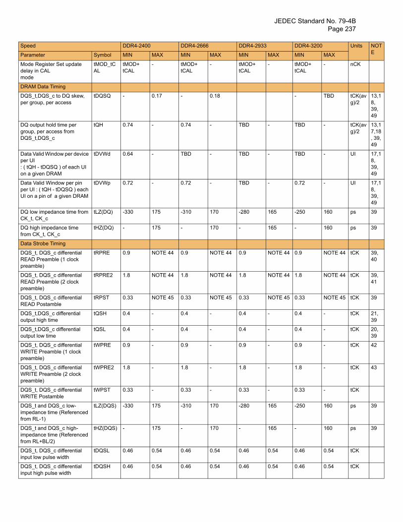
JEDEC Standard No. 79-4B Page 237
Mode Redelay in Cmode
DRAM Da
DQS_t,Dper group
v 13,18, 39, 49
DQ outpugroup, peDQS_t,DQ
v 13,17,18, 39, 49
Data Validper UI: ( tQH - ton a give
17,18, 39, 49
Data Validper UI : ( UI on a p
17,18, 39, 49
DQ low imCK_t, CK
39
DQ high ifrom CK_
39
Data Stro
DQS_t, DREAD Prpreamble
39, 40
DQS_t, DREAD Prpreamble
39, 41
DQS_t, DREAD Po
39
DQS_t,Doutput hig
21, 39
DQS_t,Doutput low
20, 39
DQS_t, DWRITE Ppreamble
42
DQS_t, DWRITE Ppreamble
43
DQS_t, DWRITE P
DQS_t animpedancfrom RL-1
39
DQS_t animpedancfrom RL+
39
DQS_t, Dinput low
DQS_t, Dinput high
Speed NOTEParamete
gister Set update AL
tMOD_tCAL
tMOD+tCAL
- tMOD+tCAL
- tMOD+tCAL
- tMOD+tCAL
- nCK
ta Timing
QS_c to DQ skew, , per access
tDQSQ - 0.17 - 0.18 - TBD tCK(ag)/2
t hold time per r access from S_c
tQH 0.74 - 0.74 - TBD - TBD - tCK(ag)/2
Window per device
DQSQ ) of each UI n DRAM
tDVWd 0.64 - TBD - TBD - TBD - UI
Window per pin tQH - tDQSQ ) each in of a given DRAM
tDVWp 0.72 - 0.72 - TBD - 0.72 - UI
pedance time from _c
tLZ(DQ) -330 175 -310 170 -280 165 -250 160 ps
mpedance time t, CK_c
tHZ(DQ) - 175 - 170 - 165 - 160 ps
be Timing
QS_c differential eamble (1 clock )
tRPRE 0.9 NOTE 44 0.9 NOTE 44 0.9 NOTE 44 0.9 NOTE 44 tCK
QS_c differential eamble (2 clock )
tRPRE2 1.8 NOTE 44 1.8 NOTE 44 1.8 NOTE 44 1.8 NOTE 44 tCK
QS_c differential stamble
tRPST 0.33 NOTE 45 0.33 NOTE 45 0.33 NOTE 45 0.33 NOTE 45 tCK
QS_c differential h time
tQSH 0.4 - 0.4 - 0.4 - 0.4 - tCK
QS_c differential time
tQSL 0.4 - 0.4 - 0.4 - 0.4 - tCK
QS_c differential reamble (1 clock )
tWPRE 0.9 - 0.9 - 0.9 - 0.9 - tCK
QS_c differential reamble (2 clock )
tWPRE2 1.8 - 1.8 - 1.8 - 1.8 - tCK
QS_c differential ostamble
tWPST 0.33 - 0.33 - 0.33 - 0.33 - tCK
d DQS_c low-e time (Referenced )
tLZ(DQS) -330 175 -310 170 -280 165 -250 160 ps
d DQS_c high-e time (Referenced BL/2)
tHZ(DQS) - 175 - 170 - 165 - 160 ps
QS_c differential pulse width
tDQSL 0.46 0.54 0.46 0.54 0.46 0.54 0.46 0.54 tCK
QS_c differential pulse width
tDQSH 0.46 0.54 0.46 0.54 0.46 0.54 0.46 0.54 tCK
DDR4-2400 DDR4-2666 DDR4-2933 DDR4-3200 Units
r Symbol MIN MAX MIN MAX MIN MAX MIN MAX
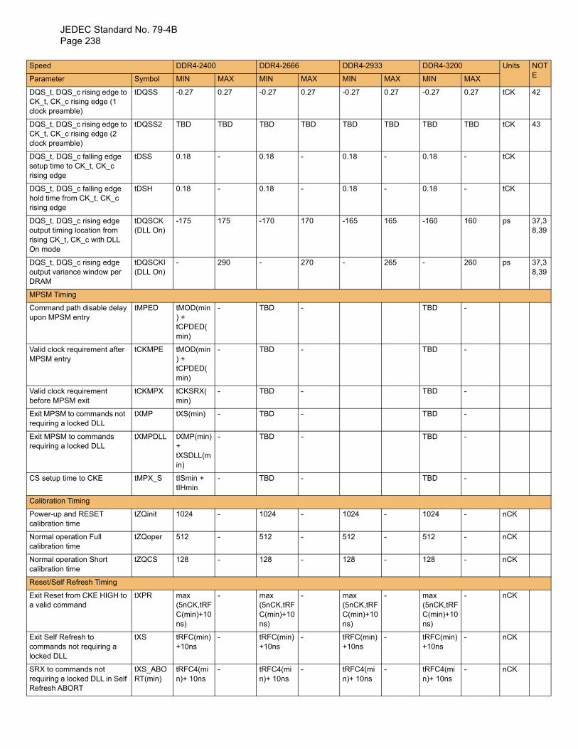
JEDEC Standard No. 79-4BPage 238
DQS_t, DCK_t, CKclock prea
42
DQS_t, DCK_t, CKclock prea
43
DQS_t, Dsetup timrising edg
DQS_t, Dhold timerising edg
DQS_t, Doutput timrising CKOn mode
37,38,39
DQS_t, Doutput vaDRAM
37,38,39
MPSM Ti
Commanupon MPS
Valid clocMPSM en
Valid clocbefore MP
Exit MPSrequiring
Exit MPSrequiring
CS setup
Calibratio
Power-upcalibration
Normal ocalibration
Normal ocalibration
Reset/Se
Exit Resea valid co
Exit Self Rcommandlocked DL
SRX to corequiring Refresh A
Speed NOTEParamete
QS_c rising edge to _c rising edge (1 mble)
tDQSS -0.27 0.27 -0.27 0.27 -0.27 0.27 -0.27 0.27 tCK
QS_c rising edge to _c rising edge (2 mble)
tDQSS2 TBD TBD TBD TBD TBD TBD TBD TBD tCK
QS_c falling edge e to CK_t, CK_c e
tDSS 0.18 - 0.18 - 0.18 - 0.18 - tCK
QS_c falling edge from CK_t, CK_c e
tDSH 0.18 - 0.18 - 0.18 - 0.18 - tCK
QS_c rising edge ing location from
_t, CK_c with DLL
tDQSCK(DLL On)
-175 175 -170 170 -165 165 -160 160 ps
QS_c rising edge riance window per
tDQSCKI(DLL On)
- 290 - 270 - 265 - 260 ps
ming
d path disable delay M entry
tMPED tMOD(min) + tCPDED(min)
- TBD - TBD -
k requirement after try
tCKMPE tMOD(min) + tCPDED(min)
- TBD - TBD -
k requirement SM exit
tCKMPX tCKSRX(min)
- TBD - TBD -
M to commands not a locked DLL
tXMP tXS(min) - TBD - TBD -
M to commands a locked DLL
tXMPDLL tXMP(min) + tXSDLL(min)
- TBD - TBD -
time to CKE tMPX_S tISmin + tIHmin
- TBD - TBD -
n Timing
and RESET time
tZQinit 1024 - 1024 - 1024 - 1024 - nCK
peration Full time
tZQoper 512 - 512 - 512 - 512 - nCK
peration Short time
tZQCS 128 - 128 - 128 - 128 - nCK
lf Refresh Timing
t from CKE HIGH to mmand
tXPR max(5nCK,tRFC(min)+10ns)
- max(5nCK,tRFC(min)+10ns)
- max(5nCK,tRFC(min)+10ns)
- max(5nCK,tRFC(min)+10ns)
- nCK
efresh to s not requiring a L
tXS tRFC(min)+10ns
- tRFC(min)+10ns
- tRFC(min)+10ns
- tRFC(min)+10ns
- nCK
mmands not a locked DLL in Self BORT
tXS_ABORT(min)
tRFC4(min)+ 10ns
- tRFC4(min)+ 10ns
- tRFC4(min)+ 10ns
- tRFC4(min)+ 10ns
- nCK
DDR4-2400 DDR4-2666 DDR4-2933 DDR4-3200 Units
r Symbol MIN MAX MIN MAX MIN MAX MIN MAX
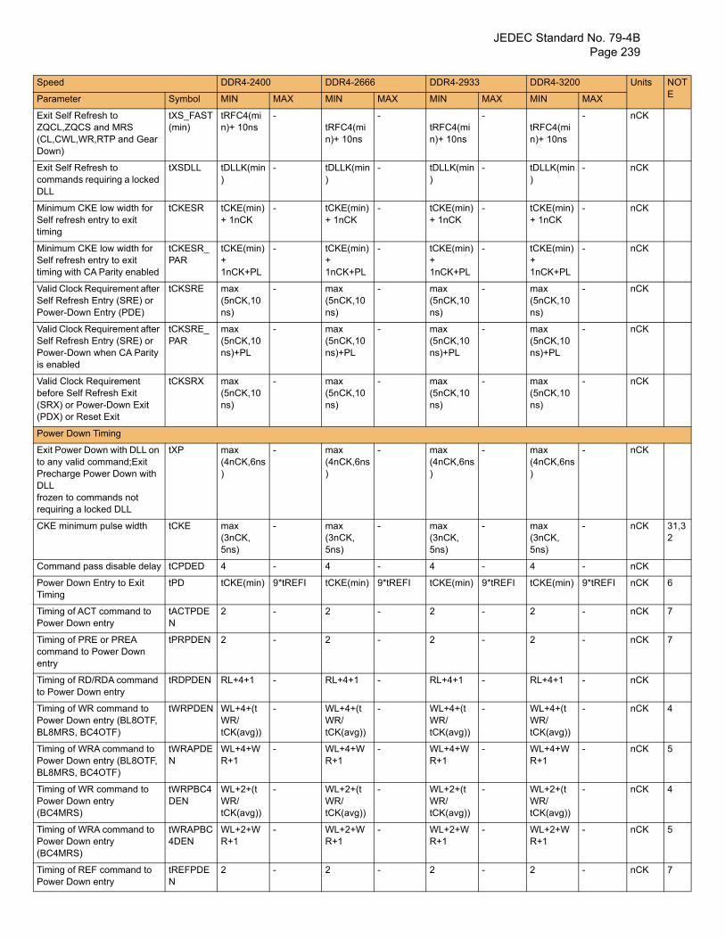
JEDEC Standard No. 79-4B Page 239
Exit Self RZQCL,ZQ(CL,CWLDown)
Exit Self RcommandDLL
MinimumSelf refretiming
MinimumSelf refretiming wit
Valid ClocSelf RefrePower-Do
Valid ClocSelf RefrePower-Dois enabled
Valid Clocbefore Se(SRX) or (PDX) or
Power Do
Exit Poweto any vaPrechargDLLfrozen to requiring
CKE mini 31,32
Comman
Power DoTiming
6
Timing ofPower Do
7
Timing ofcommandentry
7
Timing ofto Power
Timing ofPower DoBL8MRS
4
Timing ofPower DoBL8MRS
5
Timing ofPower Do(BC4MRS
4
Timing ofPower Do(BC4MRS
5
Timing ofPower Do
7
Speed NOTEParamete
efresh to CS and MRS ,WR,RTP and Gear
tXS_FAST (min)
tRFC4(min)+ 10ns
- tRFC4(min)+ 10ns
- tRFC4(min)+ 10ns
- tRFC4(min)+ 10ns
- nCK
efresh to s requiring a locked
tXSDLL tDLLK(min)
- tDLLK(min)
- tDLLK(min)
- tDLLK(min)
- nCK
CKE low width for sh entry to exit
tCKESR tCKE(min)+ 1nCK
- tCKE(min)+ 1nCK
- tCKE(min)+ 1nCK
- tCKE(min)+ 1nCK
- nCK
CKE low width for sh entry to exit h CA Parity enabled
tCKESR_ PAR
tCKE(min)+ 1nCK+PL
- tCKE(min)+ 1nCK+PL
- tCKE(min)+ 1nCK+PL
- tCKE(min)+ 1nCK+PL
- nCK
k Requirement after sh Entry (SRE) or wn Entry (PDE)
tCKSRE max(5nCK,10ns)
- max(5nCK,10ns)
- max(5nCK,10ns)
- max(5nCK,10ns)
- nCK
k Requirement after sh Entry (SRE) or wn when CA Parity
tCKSRE_PAR
max(5nCK,10ns)+PL
- max(5nCK,10ns)+PL
- max(5nCK,10ns)+PL
- max(5nCK,10ns)+PL
- nCK
k Requirement lf Refresh Exit Power-Down Exit Reset Exit
tCKSRX max(5nCK,10ns)
- max(5nCK,10ns)
- max(5nCK,10ns)
- max(5nCK,10ns)
- nCK
wn Timing
r Down with DLL on lid command;Exit e Power Down with
commands not a locked DLL
tXP max (4nCK,6ns)
- max (4nCK,6ns)
- max (4nCK,6ns)
- max (4nCK,6ns)
- nCK
mum pulse width tCKE max (3nCK, 5ns)
- max (3nCK, 5ns)
- max (3nCK, 5ns)
- max (3nCK, 5ns)
- nCK
d pass disable delay tCPDED 4 - 4 - 4 - 4 - nCK
wn Entry to Exit tPD tCKE(min) 9*tREFI tCKE(min) 9*tREFI tCKE(min) 9*tREFI tCKE(min) 9*tREFI nCK
ACT command to wn entry
tACTPDEN
2 - 2 - 2 - 2 - nCK
PRE or PREA to Power Down
tPRPDEN 2 - 2 - 2 - 2 - nCK
RD/RDA command Down entry
tRDPDEN RL+4+1 - RL+4+1 - RL+4+1 - RL+4+1 - nCK
WR command to wn entry (BL8OTF,
, BC4OTF)
tWRPDEN WL+4+(tWR/tCK(avg))
- WL+4+(tWR/tCK(avg))
- WL+4+(tWR/tCK(avg))
- WL+4+(tWR/tCK(avg))
- nCK
WRA command to wn entry (BL8OTF,
, BC4OTF)
tWRAPDEN
WL+4+WR+1
- WL+4+WR+1
- WL+4+WR+1
- WL+4+WR+1
- nCK
WR command to wn entry )
tWRPBC4DEN
WL+2+(tWR/tCK(avg))
- WL+2+(tWR/tCK(avg))
- WL+2+(tWR/tCK(avg))
- WL+2+(tWR/tCK(avg))
- nCK
WRA command to wn entry )
tWRAPBC4DEN
WL+2+WR+1
- WL+2+WR+1
- WL+2+WR+1
- WL+2+WR+1
- nCK
REF command to wn entry
tREFPDEN
2 - 2 - 2 - 2 - nCK
DDR4-2400 DDR4-2666 DDR4-2933 DDR4-3200 Units
r Symbol MIN MAX MIN MAX MIN MAX MIN MAX
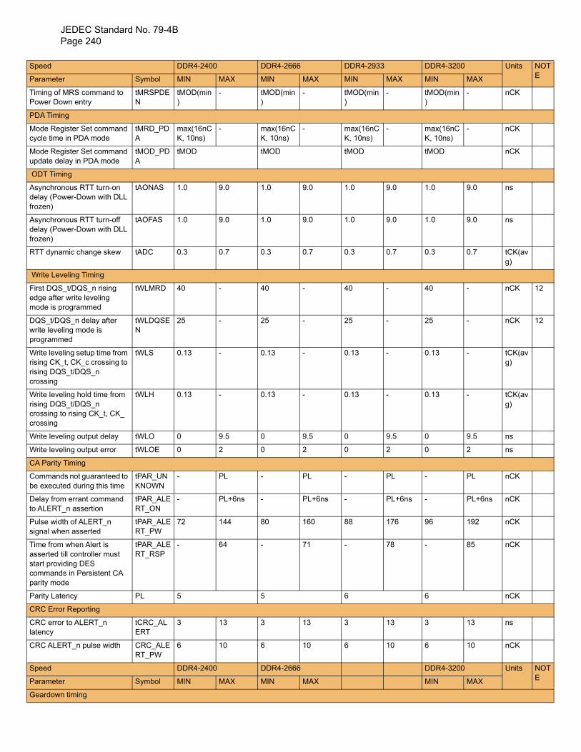
JEDEC Standard No. 79-4BPage 240
Timing ofPower Do
PDA Timi
Mode Recycle time
Mode Reupdate de
ODT Tim
Asynchrodelay (Pofrozen)
Asynchrodelay (Pofrozen)
RTT dyna v
Write Lev
First DQSedge aftemode is p
12
DQS_t/Dwrite leveprogramm
12
Write leverising CKrising DQcrossing
v
Write leverising DQcrossing crossing
v
Write leve
Write leve
CA Parity
Commanbe execu
Delay froto ALERT
Pulse widsignal wh
Time fromasserted start provcommandparity mo
Parity Lat
CRC Erro
CRC errolatency
CRC ALE
Speed NOTEParamete
Geardow
Speed NOTEParamete
MRS command to wn entry
tMRSPDEN
tMOD(min)
- tMOD(min)
- tMOD(min)
- tMOD(min)
- nCK
ng
gister Set command in PDA mode
tMRD_PDA
max(16nCK, 10ns)
- max(16nCK, 10ns)
- max(16nCK, 10ns)
- max(16nCK, 10ns)
- nCK
gister Set command lay in PDA mode
tMOD_PDA
tMOD tMOD tMOD tMOD nCK
ing
nous RTT turn-on wer-Down with DLL
tAONAS 1.0 9.0 1.0 9.0 1.0 9.0 1.0 9.0 ns
nous RTT turn-off wer-Down with DLL
tAOFAS 1.0 9.0 1.0 9.0 1.0 9.0 1.0 9.0 ns
mic change skew tADC 0.3 0.7 0.3 0.7 0.3 0.7 0.3 0.7 tCK(ag)
eling Timing
_t/DQS_n rising r write leveling rogrammed
tWLMRD 40 - 40 - 40 - 40 - nCK
QS_n delay after ling mode is ed
tWLDQSEN
25 - 25 - 25 - 25 - nCK
ling setup time from _t, CK_c crossing to S_t/DQS_n
tWLS 0.13 - 0.13 - 0.13 - 0.13 - tCK(ag)
ling hold time from S_t/DQS_n to rising CK_t, CK_
tWLH 0.13 - 0.13 - 0.13 - 0.13 - tCK(ag)
ling output delay tWLO 0 9.5 0 9.5 0 9.5 0 9.5 ns
ling output error tWLOE 0 2 0 2 0 2 0 2 ns
Timing
ds not guaranteed to ted during this time
tPAR_UNKNOWN
- PL - PL - PL - PL nCK
m errant command _n assertion
tPAR_ALERT_ON
- PL+6ns - PL+6ns - PL+6ns - PL+6ns nCK
th of ALERT_n en asserted
tPAR_ALERT_PW
72 144 80 160 88 176 96 192 nCK
when Alert is till controller must iding DES s in Persistent CA de
tPAR_ALERT_RSP
- 64 - 71 - 78 - 85 nCK
ency PL 5 5 6 6 nCK
r Reporting
r to ALERT_n tCRC_ALERT
3 13 3 13 3 13 3 13 ns
RT_n pulse width CRC_ALERT_PW
6 10 6 10 6 10 6 10 nCK
DDR4-2400 DDR4-2666 DDR4-3200 Units
r Symbol MIN MAX MIN MAX MIN MAX
n timing
DDR4-2400 DDR4-2666 DDR4-2933 DDR4-3200 Units
r Symbol MIN MAX MIN MAX MIN MAX MIN MAX
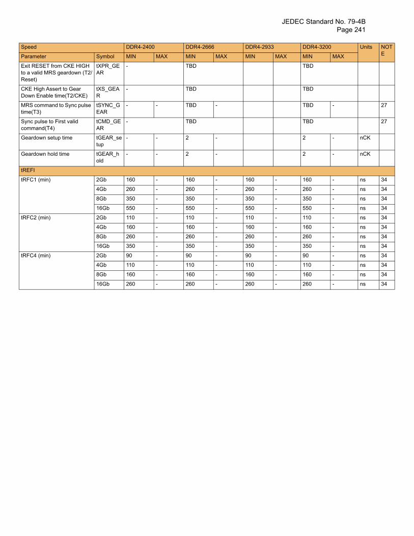
JEDEC Standard No. 79-4B Page 241
Exit RESEto a valid Reset)
CKE HighDown En
MRS comtime(T3)
27
Sync pulscommand
27
Geardow
Geardow
tREFI
tRFC1 (m 34
34
34
34
tRFC2 (m 34
34
34
34
tRFC4 (m 34
34
34
34
Speed NOTEParamete
T from CKE HIGH MRS geardown (T2/
tXPR_GEAR
- TBD TBD
Assert to Gear able time(T2/CKE)
tXS_GEAR
- TBD TBD
mand to Sync pulse tSYNC_GEAR
- - TBD - TBD -
e to First valid (T4)
tCMD_GEAR
- TBD TBD
n setup time tGEAR_setup
- - 2 - 2 - nCK
n hold time tGEAR_hold
- - 2 - 2 - nCK
in) 2Gb 160 - 160 - 160 - 160 - ns
4Gb 260 - 260 - 260 - 260 - ns
8Gb 350 - 350 - 350 - 350 - ns
16Gb 550 - 550 - 550 - 550 - ns
in) 2Gb 110 - 110 - 110 - 110 - ns
4Gb 160 - 160 - 160 - 160 - ns
8Gb 260 - 260 - 260 - 260 - ns
16Gb 350 - 350 - 350 - 350 - ns
in) 2Gb 90 - 90 - 90 - 90 - ns
4Gb 110 - 110 - 110 - 110 - ns
8Gb 160 - 160 - 160 - 160 - ns
16Gb 260 - 260 - 260 - 260 - ns
DDR4-2400 DDR4-2666 DDR4-2933 DDR4-3200 Units
r Symbol MIN MAX MIN MAX MIN MAX MIN MAX
JEDEC Standard No. 79-4BPage 242
Notes to Table 132 and Table 1331. Start of internal write transaction is defined as follows:For BL8 (Fixed by MRS and on-the-fly) : Rising clock edge 4 clock cycles after WL.For BC4 (on-the-fly) : Rising clock edge 4 clock cycles after WL.For BC4 (fixed by MRS) : Rising clock edge 2 clock cycles after WL.2. A separate timing parameter will cover the delay from write to read when CRC and DM are simultaneously enabled3. Commands requiring a locked DLL are: READ (and RAP) and synchronous ODT commands.4. tWR is defined in ns, for calculation of tWRPDEN it is necessary to round up tWR/tCK following rounding algorithm defined in Section 13.5. 5. WR in clock cycles as programmed in MR0.6. tREFI depends on TOPER.7. CKE is allowed to be registered low while operations such as row activation, precharge, autoprecharge or refresh are in progress, but power-down IDD spec will not be applied until finishing those operations.8. For these parameters, the DDR4 SDRAM device supports tnPARAM[nCK]=RU{tPARAM[ns]/tCK(avg)[ns]}, which is in clock cycles assuming all input clock jitter specifications are satisfied.
9. When CRC and DM are both enabled, tWR_CRC_DM is used in place of tWR.10. When CRC and DM are both enabled tWTR_S_CRC_DM is used in place of tWTR_S.11. When CRC and DM are both enabled tWTR_L_CRC_DM is used in place of tWTR_L.12. The max values are system dependent. 13. DQ to DQS total timing per group where the total includes the sum of deterministic and random timing terms for a specified BER. BER spec and measurement method are TBD.14. The deterministic component of the total timing. Measurement method TBD.15. DQ to DQ static offset relative to strobe per group. Measurement method TBD. 16. This parameter will be characterized and guaranteed by design.17 When the device is operated with the input clock jitter, this parameter needs to be derated by the actual tjit(per)_total of the input clock. (output deratings are relative to the SDRAM input clock). Example tbd.18. DRAM DBI mode is off.19. DRAM DBI mode is enabled. Applicable to x8 and x16 DRAM only. 20. tQSL describes the instantaneous differential output low pulse width on DQS_t - DQS_c, as measured from on falling edge to the next consecutive rising edge.21. tQSH describes the instantaneous differential output high pulse width on DQS_t - DQS_c, as measured from on falling edge to the next consecutive rising edge. 22. There is no maximum cycle time limit besides the need to satisfy the refresh interval tREFI.23. tCH(abs) is the absolute instantaneous clock high pulse width, as measured from one rising edge to the following falling edge.24. tCL(abs) is the absolute instantaneous clock low pulse width, as measured from one falling edge to the following rising edge.25. Total jitter includes the sum of deterministic and random jitter terms for a specified BER. BER target and measurement method are TBD.26. The deterministic jitter component out of the total jitter. This parameter is characterized and gauranteed by design. 27. This parameter has to be even number of clocks28. When CRC and DM are both enabled, tWR_CRC_DM is used in place of tWR.29. When CRC and DM are both enabled tWTR_S_CRC_DM is used in place of tWTR_S.30. When CRC and DM are both enabled tWTR_L_CRC_DM is used in place of tWTR_L.31. After CKE is registered LOW, CKE signal level shall be maintained below VILDC for tCKE specification (Low pulse width). 32. After CKE is registered HIGH, CKE signal level shall be maintained above VIHDC for tCKE specification (HIGH pulse width). 33. Defined between end of MPR read burst and MRS which reloads MPR or disables MPR function.34. Parameters apply from tCK(avg)min to tCK(avg)max at all standard JEDEC clock period values as stated in the Speed Bin Tables.
35. This parameter must keep consistency with Speed-Bin Tables shown in section 10.36. DDR4-1600 AC timing apply if DRAM operates at lower than 1600 MT/s data rate. UI=tCK(avg).min/237. applied when DRAM is in DLL ON mode.38. Assume no jitter on input clock signals to the DRAM.39. Value is only valid for RONNOM = 34 ohms.
40. 1tCK toggle mode with setting MR4:A11 to 0.41. 2tCK toggle mode with setting MR4:A11 to 1, which is valid for DDR4-2400/2666/3200 speed grade.42. 1tCK mode with setting MR4:A12 to 0.43. 2tCK mode with setting MR4:A12 to 1, which is valid for DDR4-2400/2666/3200 speed grade.44. The maximum read preamble is bounded by tLZ(DQS)min on the left side and tDQSCK(max) on the right side. See Figure 70 on page 92 “Clock to Data Strobe Relationship”. Boundary of DQS Low-Z occur one cycle earlier in 2tCK toggle mode which is illustrated in Section 4.20.2 “Read Preamble”.45. DQ falling signal middle-point of transferring from High to Low to first rising edge of DQS diff-signal cross-point.46. last falling edge of DQS diff-signal cross-point to DQ rising signal middle-point of transferring from Low to High.47. VrefDQ value must be set to either its midpoint or Vcent_DQ(midpoint) in order to capture DQ0 or DQL0 low level for entering PDA mode.48. The maximum read postamble is bound by tDQSCK(min) plus tQSH(min) on the left side and tHZ(DQS)max on the right side. See Figure 70 on page 92. 49. Reference level of DQ output signal is specified with a midpoint as a widest part of Output signal eye which should be approximately 0.7 * VDDQ as a center level of the static single-ended output peak-to-peak swing with a driver impedance of 34 ohms and an effective test load of 50 ohms to VTT = VDDQ.50. For MR7 commands, the minimum delay to a subsequent non-MRS command is 5nCK.
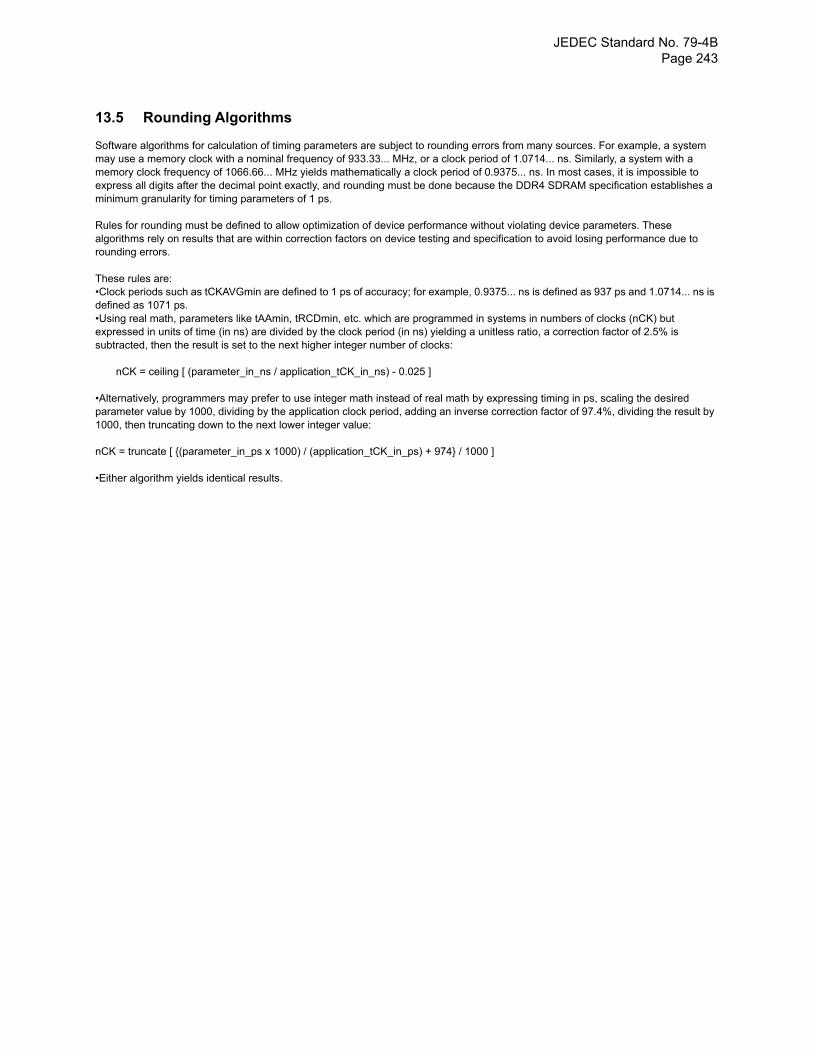
JEDEC Standard No. 79-4B Page 243
13.5 Rounding Algorithms
Software algorithms for calculation of timing parameters are subject to rounding errors from many sources. For example, a system may use a memory clock with a nominal frequency of 933.33... MHz, or a clock period of 1.0714... ns. Similarly, a system with a memory clock frequency of 1066.66... MHz yields mathematically a clock period of 0.9375... ns. In most cases, it is impossible to express all digits after the decimal point exactly, and rounding must be done because the DDR4 SDRAM specification establishes aminimum granularity for timing parameters of 1 ps.
Rules for rounding must be defined to allow optimization of device performance without violating device parameters. These algorithms rely on results that are within correction factors on device testing and specification to avoid losing performance due to rounding errors.
These rules are:•Clock periods such as tCKAVGmin are defined to 1 ps of accuracy; for example, 0.9375... ns is defined as 937 ps and 1.0714... ns is defined as 1071 ps.•Using real math, parameters like tAAmin, tRCDmin, etc. which are programmed in systems in numbers of clocks (nCK) but expressed in units of time (in ns) are divided by the clock period (in ns) yielding a unitless ratio, a correction factor of 2.5% is subtracted, then the result is set to the next higher integer number of clocks:
nCK = ceiling [ (parameter_in_ns / application_tCK_in_ns) - 0.025 ]
•Alternatively, programmers may prefer to use integer math instead of real math by expressing timing in ps, scaling the desired parameter value by 1000, dividing by the application clock period, adding an inverse correction factor of 97.4%, dividing the result by 1000, then truncating down to the next lower integer value:
nCK = truncate [ {(parameter_in_ps x 1000) / (application_tCK_in_ps) + 974} / 1000 ]
•Either algorithm yields identical results.
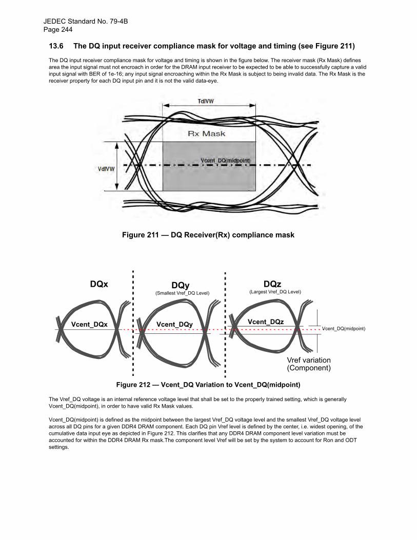
JEDEC Standard No. 79-4BPage 244
13.6 The DQ input receiver compliance mask for voltage and timing (see Figure 211)
The DQ input receiver compliance mask for voltage and timing is shown in the figure below. The receiver mask (Rx Mask) defines area the input signal must not encroach in order for the DRAM input receiver to be expected to be able to successfully capture a valid input signal with BER of 1e-16; any input signal encroaching within the Rx Mask is subject to being invalid data. The Rx Mask is the receiver property for each DQ input pin and it is not the valid data-eye.
Figure 211 — DQ Receiver(Rx) compliance mask
Figure 212 — Vcent_DQ Variation to Vcent_DQ(midpoint)
The Vref_DQ voltage is an internal reference voltage level that shall be set to the properly trained setting, which is generally Vcent_DQ(midpoint), in order to have valid Rx Mask values.
Vcent_DQ(midpoint) is defined as the midpoint between the largest Vref_DQ voltage level and the smallest Vref_DQ voltage level across all DQ pins for a given DDR4 DRAM component. Each DQ pin Vref level is defined by the center, i.e. widest opening, of the cumulative data input eye as depicted in Figure 212. This clarifies that any DDR4 DRAM component level variation must be accounted for within the DDR4 DRAM Rx mask.The component level Vref will be set by the system to account for Ron and ODT settings.
DQx DQy DQz
Vcent_DQx Vcent_DQy Vcent_DQz
Vref variation(Component)
(Smallest Vref_DQ Level) (Largest Vref_DQ Level)
Vcent_DQ(midpoint)
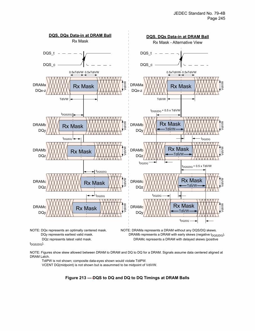
JEDEC Standard No. 79-4B Page 245
NOTE: DQx represents an optimally centered mask. NOTE: DRAMa represents a DRAM without any DQS/DQ skews. DQy represents earliest valid mask. DRAMb represents a DRAM with early skews (negative tDQS2DQ).
DQz represents latest valid mask. DRAMc represents a DRAM with delayed skews (positive tDQS2DQ).
NOTE: Figures show skew allowed between DRAM to DRAM and DQ to DQ for a DRAM. Signals assume data centered aligned at DRAM Latch. TdiPW is not shown; composite data-eyes shown would violate TdiPW. VCENT DQ(midpoint) is not shown but is assummed to be midpoint of VdiVW.
Figure 213 — DQS to DQ and DQ to DQ Timings at DRAM Balls
DQS_t
DQS_c
DQS_t
DQS_c
Rx Mask
0.5xTdiVW 0.5xTdiVW
TdiVW
DQS, DQs Data-in at DRAM BallRx Mask
DQS, DQs Data-in at DRAM BallRx Mask - Alternative View
DQx-z
DRAMa
Vd
iVW
Rx Mask
0.5xTdiVW 0.5xTdiVW
TdiVW
DQx-z
DRAMa
Vd
iVW
Rx Mask
tDQS2DQ
tDQ2DQ
DQy
DRAMbV
diV
W
Rx MaskDQz
DRAMb
Vdi
VW
Rx Mask
tDQS2DQ
tDQ2DQ
DQz
DRAMc
Vdi
VW
Rx MaskDQy
DRAMc
Vd
iVW
Rx Mask
tDQS2DQ + 0.5 x TdiVW
tDQ2DQ
DQy
DRAMb
Vd
iVW
DQz
DRAMb
Vdi
VW
tDQS2DQ + 0.5 x TdiVW
tDQ2DQ
DQz
DRAMc
Vdi
VW
DQy
DRAMc
Vd
iVW
TdiVW
tDQ2DQ
Rx MaskTdiVW
Rx MaskTdiVW
Rx MaskTdiVW
tDQ2DQ
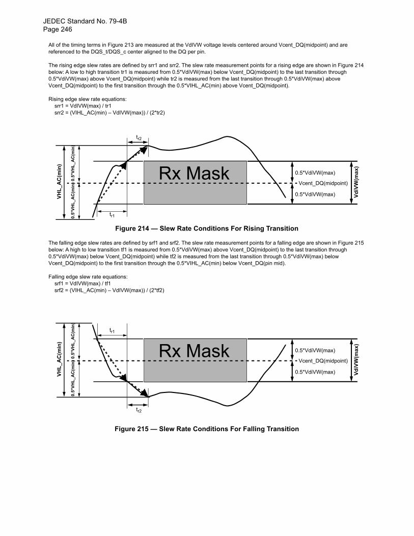
JEDEC Standard No. 79-4BPage 246
All of the timing terms in Figure 213 are measured at the VdIVW voltage levels centered around Vcent_DQ(midpoint) and are referenced to the DQS_t/DQS_c center aligned to the DQ per pin.
The rising edge slew rates are defined by srr1 and srr2. The slew rate measurement points for a rising edge are shown in Figure 214 below: A low to high transition tr1 is measured from 0.5*VdiVW(max) below Vcent_DQ(midpoint) to the last transition through 0.5*VdiVW(max) above Vcent_DQ(midpoint) while tr2 is measured from the last transition through 0.5*VdiVW(max) above Vcent_DQ(midpoint) to the first transition through the 0.5*VIHL_AC(min) above Vcent_DQ(midpoint).
Rising edge slew rate equations: srr1 = VdIVW(max) / tr1 srr2 = (VIHL_AC(min) – VdIVW(max)) / (2*tr2)
Figure 214 — Slew Rate Conditions For Rising Transition
The falling edge slew rates are defined by srf1 and srf2. The slew rate measurement points for a falling edge are shown in Figure 215 below: A high to low transition tf1 is measured from 0.5*VdiVW(max) above Vcent_DQ(midpoint) to the last transition through 0.5*VdiVW(max) below Vcent_DQ(midpoint) while tf2 is measured from the last transition through 0.5*VdiVW(max) below Vcent_DQ(midpoint) to the first transition through the 0.5*VIHL_AC(min) below Vcent_DQ(pin mid).
Falling edge slew rate equations: srf1 = VdIVW(max) / tf1 srf2 = (VIHL_AC(min) – VdIVW(max)) / (2*tf2)
Figure 215 — Slew Rate Conditions For Falling Transition
VH
L_
AC
(min
)
0.5*
VH
L_A
C(m
in)
0.5*
VH
L_A
C(m
in)
tr1
tr2
0.5*VdiVW(max)
0.5*VdiVW(max)
Vcent_DQ(midpoint)
Vd
iVW
(ma
x)Rx Mask
VH
L_A
C(m
in)
0.5*
VH
L_A
C(m
in)
0.5*
VH
L_A
C(m
in)
tr1
tr2
0.5*VdiVW(max)
0.5*VdiVW(max)
Vcent_DQ(midpoint)V
diV
W(m
ax)Rx Mask
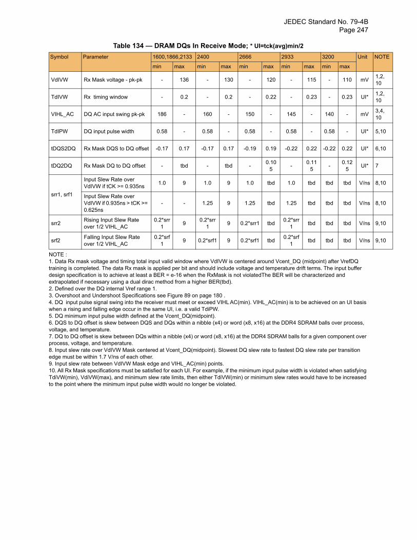
JEDEC Standard No. 79-4B Page 247
NOTE
1,2, 10
1,2,10
3,4,10
5,10
6,10
7
8,10
8,10
9,10
9,10
Table 134 — DRAM DQs In Receive Mode; * UI=tck(avg)min/2
NOTE : 1. Data Rx mask voltage and timing total input valid window where VdIVW is centered around Vcent_DQ (midpoint) after VrefDQ training is completed. The data Rx mask is applied per bit and should include voltage and temperature drift terms. The input buffer design specification is to achieve at least a BER = e-16 when the RxMask is not violatedThe BER will be characterized and extrapolated if necessary using a dual dirac method from a higher BER(tbd).2. Defined over the DQ internal Vref range 1. 3. Overshoot and Undershoot Specifications see Figure 89 on page 180 .4. DQ input pulse signal swing into the receiver must meet or exceed VIHL AC(min). VIHL_AC(min) is to be achieved on an UI basis when a rising and falling edge occur in the same UI, i.e. a valid TdiPW.5. DQ minimum input pulse width defined at the Vcent_DQ(midpoint). 6. DQS to DQ offset is skew between DQS and DQs within a nibble (x4) or word (x8, x16) at the DDR4 SDRAM balls over process, voltage, and temperature.7. DQ to DQ offset is skew between DQs within a nibble (x4) or word (x8, x16) at the DDR4 SDRAM balls for a given component over process, voltage, and temperature.8. Input slew rate over VdIVW Mask centered at Vcent_DQ(midpoint). Slowest DQ slew rate to fastest DQ slew rate per transition edge must be within 1.7 V/ns of each other. 9. Input slew rate between VdIVW Mask edge and VIHL_AC(min) points.10. All Rx Mask specifications must be satisfied for each UI. For example, if the minimum input pulse width is violated when satisfying TdiVW(min), VdiVW(max), and minimum slew rate limits, then either TdiVW(min) or minimum slew rates would have to be increased to the point where the minimum input pulse width would no longer be violated.
Symbol Parameter 1600,1866,2133 2400 2666 2933 3200 Unit
min max min max min max min max min max
VdIVW Rx Mask voltage - pk-pk - 136 - 130 - 120 - 115 - 110 mV
TdIVW Rx timing window - 0.2 - 0.2 - 0.22 - 0.23 - 0.23 UI*
VIHL_AC DQ AC input swing pk-pk 186 - 160 - 150 - 145 - 140 - mV
TdIPW DQ input pulse width 0.58 - 0.58 - 0.58 - 0.58 - 0.58 - UI*
tDQS2DQ Rx Mask DQS to DQ offset -0.17 0.17 -0.17 0.17 -0.19 0.19 -0.22 0.22 -0.22 0.22 UI*
tDQ2DQ Rx Mask DQ to DQ offset - tbd - tbd -0.10
5-
0.115
-0.12
5UI*
srr1, srf1
Input Slew Rate over VdIVW if tCK >= 0.935ns
1.0 9 1.0 9 1.0 tbd 1.0 tbd tbd tbd V/ns
Input Slew Rate overVdIVW if 0.935ns > tCK >= 0.625ns
- - 1.25 9 1.25 tbd 1.25 tbd tbd tbd V/ns
srr2Rising Input Slew Rateover 1/2 VIHL_AC
0.2*srr1
90.2*srr
19 0.2*srr1 tbd
0.2*srr1
tbd tbd tbd V/ns
srf2Falling Input Slew Rateover 1/2 VIHL_AC
0.2*srf1
9 0.2*srf1 9 0.2*srf1 tbd0.2*srf
1tbd tbd tbd V/ns
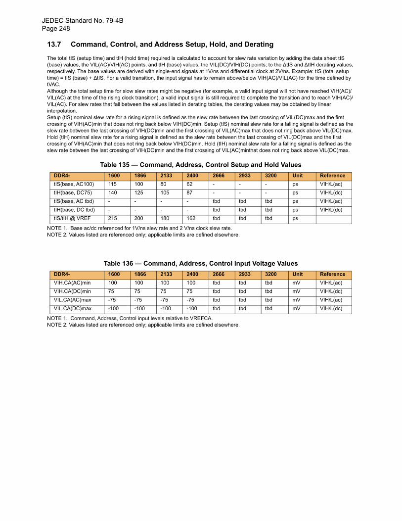
JEDEC Standard No. 79-4BPage 248
13.7 Command, Control, and Address Setup, Hold, and Derating
The total tIS (setup time) and tIH (hold time) required is calculated to account for slew rate variation by adding the data sheet tIS (base) values, the VIL(AC)/VIH(AC) points, and tIH (base) values, the VIL(DC)/VIH(DC) points; to the ΔtIS and ΔtIH derating values, respectively. The base values are derived with single-end signals at 1V/ns and differential clock at 2V/ns. Example: tIS (total setup time) = tIS (base) + ΔtIS. For a valid transition, the input signal has to remain above/below VIH(AC)/VIL(AC) for the time defined by tVAC.Although the total setup time for slow slew rates might be negative (for example, a valid input signal will not have reached VIH(AC)/VIL(AC) at the time of the rising clock transition), a valid input signal is still required to complete the transition and to reach VIH(AC)/VIL(AC). For slew rates that fall between the values listed in derating tables, the derating values may be obtained by linear interpolation.Setup (tIS) nominal slew rate for a rising signal is defined as the slew rate between the last crossing of VIL(DC)max and the first crossing of VIH(AC)min that does not ring back below VIH(DC)min. Setup (tIS) nominal slew rate for a falling signal is defined as the slew rate between the last crossing of VIH(DC)min and the first crossing of VIL(AC)max that does not ring back above VIL(DC)max.Hold (tIH) nominal slew rate for a rising signal is defined as the slew rate between the last crossing of VIL(DC)max and the first crossing of VIH(AC)min that does not ring back below VIH(DC)min. Hold (tIH) nominal slew rate for a falling signal is defined as the slew rate between the last crossing of VIH(DC)min and the first crossing of VIL(AC)minthat does not ring back above VIL(DC)max.
Table 135 — Command, Address, Control Setup and Hold Values
NOTE 1. Base ac/dc referenced for 1V/ns slew rate and 2 V/ns clock slew rate.NOTE 2. Values listed are referenced only; applicable limits are defined elsewhere.
Table 136 — Command, Address, Control Input Voltage Values
NOTE 1. Command, Address, Control input levels relative to VREFCA.NOTE 2. Values listed are referenced only; applicable limits are defined elsewhere.
DDR4- 1600 1866 2133 2400 2666 2933 3200 Unit Reference
tIS(base, AC100) 115 100 80 62 - - - ps VIH/L(ac)
tIH(base, DC75) 140 125 105 87 - - - ps VIH/L(dc)
tIS(base, AC tbd) - - - - tbd tbd tbd ps VIH/L(ac)
tIH(base, DC tbd) - - - - tbd tbd tbd ps VIH/L(dc)
tIS/tIH @ VREF 215 200 180 162 tbd tbd tbd ps
DDR4- 1600 1866 2133 2400 2666 2933 3200 Unit Reference
VIH.CA(AC)min 100 100 100 100 tbd tbd tbd mV VIH/L(ac)
VIH.CA(DC)min 75 75 75 75 tbd tbd tbd mV VIH/L(dc)
VIL.CA(AC)max -75 -75 -75 -75 tbd tbd tbd mV VIH/L(ac)
VIL.CA(DC)max -100 -100 -100 -100 tbd tbd tbd mV VIH/L(dc)
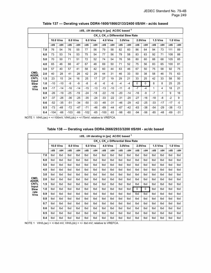
JEDEC Standard No. 79-4B Page 249
Table 137 — Derating values DDR4-1600/1866/2133/2400 tIS/tIH - ac/dc based
NOTE 1 VIH/L(ac) = +/-100mV, VIH/L(dc) = +/-75mV; relative to VREFCA.
Table 138 — Derating values DDR4-2666/2933/3200 tIS/tIH - ac/dc based
NOTE 1 VIH/L(ac) = +/-tbd mV, VIH/L(dc) = +/- tbd mV; relative to VREFCA.
tIS, IH derating in [ps] AC/DC based 1
CK_t, CK_c Differential Slew Rate
10.0 V/ns 8.0 V/ns 6.0 V/ns 4.0 V/ns 3.0V/ns 2.0V/ns 1.5 V/ns 1.0 V/ns
tIS tIH tIS tIH tIS tIH tIS tIH tIS tIH tIS tIH tIS tIH tIS tIH
CMD, ADDR, CNTL Input Slew rate V/ns
7.0 76 54 76 55 77 56 79 58 82 60 86 64 94 73 111 89
6.0 73 53 74 53 75 54 77 56 79 58 83 63 92 71 108 88
5.0 70 50 71 51 72 52 74 54 76 56 80 60 88 68 105 85
4.0 65 46 66 47 67 48 69 50 71 52 75 56 83 65 100 81
3.0 57 40 57 41 58 42 60 44 63 46 67 50 75 58 92 75
2.0 40 28 41 28 42 29 44 31 46 33 50 38 58 46 75 63
1.5 23 15 24 16 25 17 27 19 29 21 33 25 42 33 58 50
1.0 -10 -10 -9 -9 -8 -8 -6 -6 -4 -4 0 0 8 8 25 25
0.9 -17 -14 -16 -14 -15 -13 -13 -10 -11 -8 -7 -4 1 4 18 21
0.8 -26 -19 -25 -19 -24 -18 -22 -16 -20 -14 -16 -9 -7 -1 9 16
0.7 -37 -26 -36 -25 -35 -24 -33 -22 -31 -20 -27 -16 -18 -8 -2 9
0.6 -52 -35 -51 -34 -50 -33 -48 -31 -46 -29 -42 -25 -33 -17 -17 -0
0.5 -73 -48 -72 -47 -71 -46 -69 -44 -67 -42 -63 -38 -54 -29 -38 -13
0.4 -104 -66 -103 -66 -102 -65 -100 -63 -98 -60 -94 -56 -85 -48 -69 -31
tIS, IH derating in [ps] AC/DC based 1
CK_t, CK_c Differential Slew Rate
10.0 V/ns 8.0 V/ns 6.0 V/ns 4.0 V/ns 3.0V/ns 2.0V/ns 1.5 V/ns 1.0 V/ns
tIS tIH tIS tIH tIS tIH tIS tIH tIS tIH tIS tIH tIS tIH tIS tIH
CMD, ADDR, CNTL Input Slew rate V/ns
7.0 tbd tbd tbd tbd tbd tbd tbd tbd tbd tbd tbd tbd tbd tbd tbd tbd
6.0 tbd tbd tbd tbd tbd tbd tbd tbd tbd tbd tbd tbd tbd tbd tbd tbd
5.0 tbd tbd tbd tbd tbd tbd tbd tbd tbd tbd tbd tbd tbd tbd tbd tbd
4.0 tbd tbd tbd tbd tbd tbd tbd tbd tbd tbd tbd tbd tbd tbd tbd tbd
3.0 tbd tbd tbd tbd tbd tbd tbd tbd tbd tbd tbd tbd tbd tbd tbd tbd
2.0 tbd tbd tbd tbd tbd tbd tbd tbd tbd tbd tbd tbd tbd tbd tbd tbd
1.5 tbd tbd tbd tbd tbd tbd tbd tbd tbd tbd tbd tbd tbd tbd tbd tbd
1.0 tbd tbd tbd tbd tbd tbd tbd tbd tbd tbd 0 0 tbd tbd tbd tbd
0.9 tbd tbd tbd tbd tbd tbd tbd tbd tbd tbd tbd tbd tbd tbd tbd tbd
0.8 tbd tbd tbd tbd tbd tbd tbd tbd tbd tbd tbd tbd tbd tbd tbd tbd
0.7 tbd tbd tbd tbd tbd tbd tbd tbd tbd tbd tbd tbd tbd tbd tbd tbd
0.6 tbd tbd tbd tbd tbd tbd tbd tbd tbd tbd tbd tbd tbd tbd tbd tbd
0.5 tbd tbd tbd tbd tbd tbd tbd tbd tbd tbd tbd tbd tbd tbd tbd tbd
0.4 tbd tbd tbd tbd tbd tbd tbd tbd tbd tbd tbd tbd tbd tbd tbd tbd
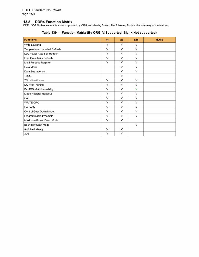
JEDEC Standard No. 79-4BPage 250
13.8 DDR4 Function MatrixDDR4 SDRAM has several features supported by ORG and also by Speed. The following Table is the summary of the features.
Table 139 — Function Matrix (By ORG. V:Supported, Blank:Not supported)
Functions x4 x8 x16 NOTE
Write Leveling V V V
Temperature controlled Refresh V V V
Low Power Auto Self Refresh V V V
Fine Granularity Refresh V V V
Multi Purpose Register V V V
Data Mask V V
Data Bus Inversion V V
TDQS V
ZQ calibration — V V V
DQ Vref Training V V V
Per DRAM Addressability V V V
Mode Register Readout V V V
CAL V V V
WRITE CRC V V V
CA Parity V V V
Control Gear Down Mode V V V
Programmable Preamble V V V
Maximum Power Down Mode V V
Boundary Scan Mode V
Additive Latency V V
3DS V V
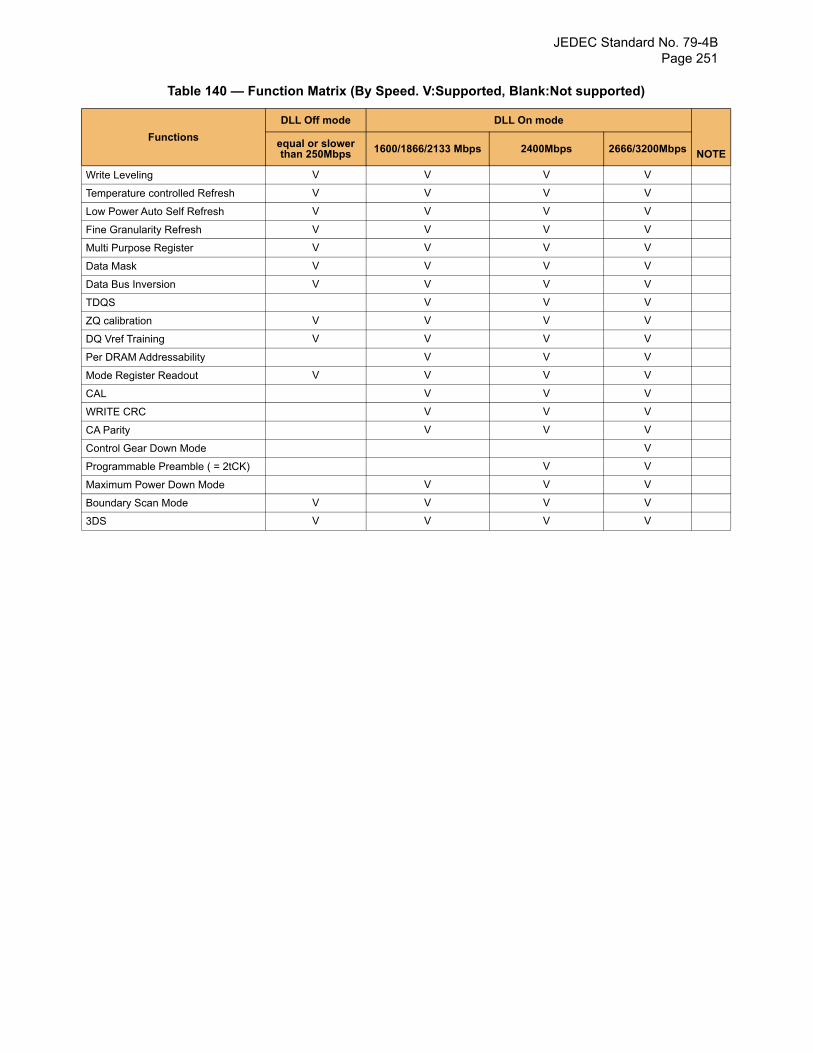
JEDEC Standard No. 79-4B Page 251
Table 140 — Function Matrix (By Speed. V:Supported, Blank:Not supported)
Functions
DLL Off mode DLL On mode
NOTEequal or slowerthan 250Mbps 1600/1866/2133 Mbps 2400Mbps 2666/3200Mbps
Write Leveling V V V V
Temperature controlled Refresh V V V V
Low Power Auto Self Refresh V V V V
Fine Granularity Refresh V V V V
Multi Purpose Register V V V V
Data Mask V V V V
Data Bus Inversion V V V V
TDQS V V V
ZQ calibration V V V V
DQ Vref Training V V V V
Per DRAM Addressability V V V
Mode Register Readout V V V V
CAL V V V
WRITE CRC V V V
CA Parity V V V
Control Gear Down Mode V
Programmable Preamble ( = 2tCK) V V
Maximum Power Down Mode V V V
Boundary Scan Mode V V V V
3DS V V V V
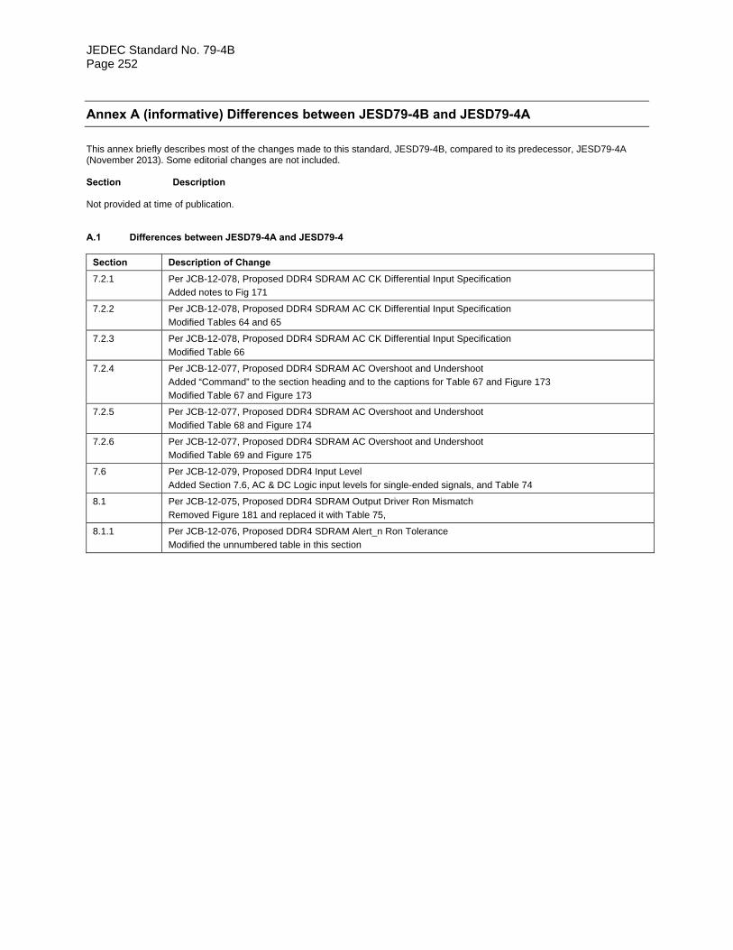
JEDEC Standard No. 79-4B Page 252
Annex A (informative) Differences between JESD79-4B and JESD79-4A This annex briefly describes most of the changes made to this standard, JESD79-4B, compared to its predecessor, JESD79-4A (November 2013). Some editorial changes are not included. Section Description Not provided at time of publication. A.1 Differences between JESD79-4A and JESD79-4
Section Description of Change
7.2.1 Per JCB-12-078, Proposed DDR4 SDRAM AC CK Differential Input Specification
Added notes to Fig 171
7.2.2 Per JCB-12-078, Proposed DDR4 SDRAM AC CK Differential Input Specification
Modified Tables 64 and 65
7.2.3 Per JCB-12-078, Proposed DDR4 SDRAM AC CK Differential Input Specification
Modified Table 66
7.2.4 Per JCB-12-077, Proposed DDR4 SDRAM AC Overshoot and Undershoot
Added “Command” to the section heading and to the captions for Table 67 and Figure 173
Modified Table 67 and Figure 173
7.2.5 Per JCB-12-077, Proposed DDR4 SDRAM AC Overshoot and Undershoot
Modified Table 68 and Figure 174
7.2.6 Per JCB-12-077, Proposed DDR4 SDRAM AC Overshoot and Undershoot
Modified Table 69 and Figure 175
7.6 Per JCB-12-079, Proposed DDR4 Input Level
Added Section 7.6, AC & DC Logic input levels for single-ended signals, and Table 74
8.1 Per JCB-12-075, Proposed DDR4 SDRAM Output Driver Ron Mismatch
Removed Figure 181 and replaced it with Table 75,
8.1.1 Per JCB-12-076, Proposed DDR4 SDRAM Alert_n Ron Tolerance
Modified the unnumbered table in this section
Rev. 8/13
Standard Improvement Form JEDEC JESD79-4B The purpose of this form is to provide the Technica l Committees of JEDEC wit h input from the indu stry regarding usage of the subje ct standard. Individuals or companies are invited to submit comment s to JEDEC. All comments will be collected and dispersed to the appropriate committee(s). If you can provide input, please complete this form and return to:
JEDEC Attn: Publications Department 3103 North 10th Street Suite 240 South Arlington, VA 22201-2107
Fax: 703.907.7583
1. I recommend changes to the following: Requirement, clause number
Test method number Clause number The referenced clause number has proven to be: Unclear Too Rigid In Error
Other
2. Recommendations for correction:
3. Other suggestions for document improvement:
Submitted by
Name: Phone:
Company: E-mail:
Address:
City/State/Zip: Date: