Embed Size (px)
Citation preview

JESD204B Intel® FPGA IP User Guide
Updated for Intel® Quartus® Prime Design Suite: 19.4
IP Version: 19.2.0
SubscribeSend Feedback
UG-01142 | 2020.03.03Latest document on the web: PDF | HTML

Contents
1. JESD204B IP Quick Reference.........................................................................................4
2. About the JESD204B Intel FPGA IP................................................................................. 62.1. Release Information...............................................................................................82.2. Device Family Support............................................................................................82.3. Datapath Modes.................................................................................................... 92.4. IP Variation...........................................................................................................92.5. JESD204B IP Configuration....................................................................................10
2.5.1. Run-Time Configuration............................................................................ 112.6. Channel Bonding..................................................................................................122.7. Performance and Resource Utilization..................................................................... 14
3. Getting Started............................................................................................................. 203.1. Introduction to Intel FPGA IP Cores........................................................................ 203.2. Installing and Licensing Intel FPGA IP Cores............................................................ 213.3. Intel FPGA IP Evaluation Mode...............................................................................223.4. Upgrading IP Cores.............................................................................................. 243.5. IP Catalog and Parameter Editor............................................................................ 283.6. Design Walkthrough............................................................................................. 28
3.6.1. Creating a New Intel Quartus Prime Project................................................. 283.6.2. Parameterizing and Generating the IP.........................................................293.6.3. Compiling the JESD204B IP Core Design..................................................... 303.6.4. Programming an FPGA Device....................................................................31
3.7. JESD204B Design Examples.................................................................................. 313.8. JESD204B IP Design Considerations....................................................................... 31
3.8.1. Integrating the JESD204B IP in Platform Designer........................................ 313.8.2. Pin Assignments...................................................................................... 333.8.3. Adding External Transceiver PLLs............................................................... 333.8.4. Timing Constraints For Input Clocks............................................................33
3.9. JESD204B Intel FPGA IP Parameters.......................................................................363.10. JESD204B IP Component Files............................................................................. 413.11. JESD204B IP Testbench...................................................................................... 41
3.11.1. Generating and Simulating the IP Testbench.............................................. 423.11.2. Testbench Simulation Flow.......................................................................45
4. JESD204B IP Functional Description............................................................................ 464.1. Transmitter......................................................................................................... 48
4.1.1. TX Data Link Layer...................................................................................494.1.2. TX PHY Layer.......................................................................................... 52
4.2. Receiver............................................................................................................. 524.2.1. RX Data Link Layer...................................................................................534.2.2. RX PHY Layer.......................................................................................... 56
4.3. Operation........................................................................................................... 564.3.1. Operating Modes......................................................................................574.3.2. Scrambler/Descrambler............................................................................ 594.3.3. SYNC_N Signal........................................................................................ 604.3.4. Link Reinitialization.................................................................................. 614.3.5. Link Startup Sequence..............................................................................62
Contents
JESD204B Intel® FPGA IP User Guide Send Feedback
2

4.3.6. Error Reporting Through SYNC_N Signal......................................................634.4. Clocking Scheme................................................................................................. 63
4.4.1. Device Clock........................................................................................... 654.4.2. Link Clock...............................................................................................674.4.3. Local MultiFrame Clock............................................................................. 684.4.4. Clock Correlation..................................................................................... 69
4.5. Reset Scheme..................................................................................................... 704.5.1. Reset Sequence.......................................................................................724.5.2. ADC–FPGA Subsystem Reset Sequence....................................................... 724.5.3. FPGA–DAC Subsystem Reset Sequence....................................................... 74
4.6. Signals...............................................................................................................764.6.1. Transmitter Signals.................................................................................. 774.6.2. Receiver Signals...................................................................................... 89
4.7. Registers............................................................................................................ 984.7.1. Register Access Type Convention................................................................994.7.2. Transmitter Registers................................................................................994.7.3. Receiver Registers..................................................................................123
5. JESD204B IP Deterministic Latency Implementation Guidelines.................................1495.1. Constraining Incoming SYSREF Signal...................................................................1495.2. Programmable RBD Offset...................................................................................1505.3. Programmable LMFC Offset..................................................................................1535.4. Maintaining Deterministic Latency during Link Reinitialization...................................157
6. JESD204B IP Debug Guidelines...................................................................................1596.1. Clocking Scheme................................................................................................1596.2. JESD204B Parameters........................................................................................ 1596.3. SPI Programming...............................................................................................1596.4. Converter and FPGA Operating Conditions............................................................. 1606.5. Signal Polarity and FPGA Pin Assignment...............................................................1606.6. Creating a Signal Tap Debug File to Match Your Design Hierarchy .............................1616.7. Debugging JESD204B Link Using System Console...................................................162
7. JESD204B Intel FPGA IP User Guide Archives............................................................. 169
8. Document Revision History for the JESD204B Intel FPGA IP User Guide.....................170
Contents
Send Feedback JESD204B Intel® FPGA IP User Guide
3

1. JESD204B IP Quick ReferenceThe JESD204B Intel FPGA IP is a high-speed point-to-point serial interface intellectualproperty (IP).
Note: For system requirements and installation instructions, refer to Intel FPGA SoftwareInstallation & Licensing.
Table 1. Brief Information About the JESD204B IP
Item Description
Protocol Features
• Joint Electron Device Engineering Council (JEDEC) JESD204B.01, 2012 standardrelease specification
• Device subclass:— Subclass 0—Backwards compatible to JESD204A.— Subclass 1—Uses SYSREF signal to support deterministic latency.— Subclass 2—Uses SYNC_N detection to support deterministic latency.
Core Features • Run-time configuration of parameters L, M, and F• Data rate of up to 12.5 gigabits per second (Gbps)—per JESD204B specification• Data rate of up to 19.2 Gbps—not certified per JESD204B specification
(uncharacterized support)• Single or multiple lanes (up to 8 lanes per link)• Serial lane alignment and monitoring• Lane synchronization• Modular design that supports multidevice synchronization• MAC and PHY partitioning• Deterministic latency support• 8B/10B encoding• Scrambling/Descrambling• Avalon® Streaming (Avalon-ST) interface for transmit and receive datapaths• Avalon Memory-Mapped (Avalon-MM) interface for Configuration and Status registers
(CSR)• Dynamic generation of simulation testbench
Typical Application • Wireless communication equipment• Broadcast equipment• Military equipment• Medical equipment• Test and measurement equipment
Device Family Support • Intel Agilex™ devices (E-tile)• Intel Cyclone® 10 GX FPGA devices• Intel Stratix® 10 FPGA devices (L-tile/H-tile/E-tile)• Intel Arria® 10 FPGA devices• Stratix V FPGA devices
continued...
UG-01142 | 2020.03.03
Send Feedback
Intel Corporation. All rights reserved. Agilex, Altera, Arria, Cyclone, Enpirion, Intel, the Intel logo, MAX, Nios,Quartus and Stratix words and logos are trademarks of Intel Corporation or its subsidiaries in the U.S. and/orother countries. Intel warrants performance of its FPGA and semiconductor products to current specifications inaccordance with Intel's standard warranty, but reserves the right to make changes to any products and servicesat any time without notice. Intel assumes no responsibility or liability arising out of the application or use of anyinformation, product, or service described herein except as expressly agreed to in writing by Intel. Intelcustomers are advised to obtain the latest version of device specifications before relying on any publishedinformation and before placing orders for products or services.*Other names and brands may be claimed as the property of others.
ISO9001:2015Registered

Item Description
• Arria V FPGA devices• Arria V GZ FPGA devices• Cyclone V FPGA devices
Design Tools • Platform Designer parameter editor in the Intel Quartus® Prime software for designcreation and compilation
• Timing Analyzer in the Intel Quartus Prime software for timing analysis• ModelSim* - Intel FPGA Edition, Riviera-PRO*, VCS*/VCS MX, NCSim, and Xcelium*
Parallel simulator software for design simulation or synthesis
Related Information
• Design Examples for JESD204B IP Core User GuideProvides information about design examples for Arria V, Cyclone V, Stratix V,and Intel Arria 10 devices using Intel Quartus Prime Standard Edition software.
• JESD204B Intel Arria 10 FPGA IP Design Example User Guide
• JESD204B Intel Stratix 10 FPGA IP Design Example User Guide
• JESD204B Intel Cyclone 10 GX FPGA IP Design Example User Guide
• JESD204B Intel Agilex FPGA IP Design Example User Guide
• Intel FPGA Software Installation and Licensing
• JESD204B IP Core Release Notes
• Errata for JESD204B IP Core in the Knowledge Base
• AN803: Implementing ADC-Intel Arria 10 Multi-Link Design with JESD204B RX IPCore
• AN804: Implementing ADC-Intel Stratix 10 Multi-Link Design with JESD204B RX IPCore
• JESD204B Intel FPGA IP User Guide Archives on page 169Provides a list of user guides for previous versions of the JESD204B IP core.
1. JESD204B IP Quick Reference
UG-01142 | 2020.03.03
Send Feedback JESD204B Intel® FPGA IP User Guide
5

2. About the JESD204B Intel FPGA IPThe JESD204B Intel FPGA IP is a high-speed point-to-point serial interface for digital-to-analog (DAC) or analog-to-digital (ADC) converters to transfer data to FPGAdevices. This unidirectional serial interface runs at a maximum data rate of 17.4 Gbps.This protocol offers higher bandwidth, low I/O count and supports scalability in bothnumber of lanes and data rates. The JESD204B Intel FPGA IP addresses multi-devicesynchronization by introducing Subclass 1 and Subclass 2 to achieve deterministiclatency.
Note: The full product name, JESD204B Intel FPGA IP, is shortened to JESD204B IP in thisdocument.
The JESD204B IP incorporates:
• Media access control (MAC)—data link layer (DLL) block that controls the linkstates and character replacement.
• Physical layer (PHY)—physical coding sublayer (PCS) and physical mediaattachment (PMA) block.
The JESD204B IP does not incorporate the Transport Layer (TL) that controls theframe assembly and disassembly. The TL and test components are provided as part ofa design example component where you can customize the design for differentconverter devices.
UG-01142 | 2020.03.03
Send Feedback
Intel Corporation. All rights reserved. Agilex, Altera, Arria, Cyclone, Enpirion, Intel, the Intel logo, MAX, Nios,Quartus and Stratix words and logos are trademarks of Intel Corporation or its subsidiaries in the U.S. and/orother countries. Intel warrants performance of its FPGA and semiconductor products to current specifications inaccordance with Intel's standard warranty, but reserves the right to make changes to any products and servicesat any time without notice. Intel assumes no responsibility or liability arising out of the application or use of anyinformation, product, or service described herein except as expressly agreed to in writing by Intel. Intelcustomers are advised to obtain the latest version of device specifications before relying on any publishedinformation and before placing orders for products or services.*Other names and brands may be claimed as the property of others.
ISO9001:2015Registered

Figure 1. Typical System Application for JESD204B IP
The JESD204B IP uses the Avalon-ST source and sink interfaces, with unidirectional flow of data, to transmitand receive data on the FPGA fabric interface.
JESD204B TXIP Core
FPGA
M Converters1 Link, L Lanes
SYNC_N
M Converters
M Converters
SYNC_N
SYNC_N
M ConvertersSYNC_N
JESD204B RXIP Core
1 Link, L Lanes
1 Link, L Lanes
1 Link, L Lanes
DAC DeviceClock 1
ADC DeviceClock 1
Multi-DeviceSynchronizationthrough Subclass 1 or Subclass 2
Multi-DeviceSynchronizationthrough Subclass 1or Subclass 2
Logic Device (TX)Device Clock 2
Logic Device (RX)Device Clock 2
JESD204B TXIP Core
JESD204B RXIP Core
Key features of the JESD204B IP:
• Data rate of up to 19.2 Gbps (characterization up to 12.5 G)
• Run-time JESD204B parameter configuration (L, M, F, S, N, K, CS, CF)
• MAC and PHY partitioning for portability
• Subclass 0 mode for backward compatibility to JESD204A
• Subclass 1 mode for deterministic latency support (using SYSREF) between theADC/DAC and logic device
• Subclass 2 mode for deterministic latency support (using SYNC_N) between theADC/DAC and logic device
• Multi-device synchronization
2. About the JESD204B Intel FPGA IP
UG-01142 | 2020.03.03
Send Feedback JESD204B Intel® FPGA IP User Guide
7

Related Information
• V-Series Transceiver PHY User Guide
• Intel Arria 10 Transceiver PHY User Guide
• Intel Cyclone 10 GX Transceiver PHY User Guide
• Intel Stratix 10 L- and H-tile Transceiver PHY User Guide
• E-tile Transceiver PHY User Guide
• Intel Agilex Device Datasheet
• Intel Stratix 10 Device Datasheet
• Intel Arria 10 Device Datasheet
2.1. Release Information
IP versions are the same as the Intel Quartus Prime Design Suite software versions upto v19.1. From Intel Quartus Prime Design Suite software version 19.2 or later, IPcores have a new IP versioning scheme.
The IP versioning scheme (X.Y.Z) number changes from one software version toanother. A change in:
• X indicates a major revision of the IP. If you update your Intel Quartus Primesoftware, you must regenerate the IP.
• Y indicates the IP includes new features. Regenerate your IP to include these newfeatures.
• Z indicates the IP includes minor changes. Regenerate your IP to include thesechanges.
Table 2. JESD204B IP Release Information
Item Description
IP Version 19.3.0
Intel Quartus Prime Version 19.4
Release Date December 2019
Ordering Code IP-JESD204B
2.2. Device Family Support
Table 3. Intel Device Family Support
Device Family Support Level
Intel Agilex (E-tile) Advance
Intel Stratix 10 (E-tile, H-tile, and L-tile) Final
Intel Arria 10 Final
Intel Cyclone 10 GX Final
continued...
2. About the JESD204B Intel FPGA IP
UG-01142 | 2020.03.03
JESD204B Intel® FPGA IP User Guide Send Feedback
8

Device Family Support Level
Stratix V Final
Arria V Final
Cyclone V Final
The following terms define device support levels for Intel FPGA IP cores:
• Advance support—the IP core is available for simulation and compilation for thisdevice family. Timing models include initial engineering estimates of delays basedon early post-layout information. The timing models are subject to change assilicon testing improves the correlation between the actual silicon and the timingmodels. You can use this IP core for system architecture and resource utilizationstudies, simulation, pinout, system latency assessments, basic timing assessments(pipeline budgeting), and I/O transfer strategy (data-path width, burst depth, I/Ostandards tradeoffs).
• Preliminary support—the IP core is verified with preliminary timing models for thisdevice family. The IP core meets all functional requirements, but might still beundergoing timing analysis for the device family. It can be used in productiondesigns with caution.
• Final support—the IP core is verified with final timing models for this device family.The IP core meets all functional and timing requirements for the device family andcan be used in production designs.
2.3. Datapath Modes
The JESD204B IP supports TX-only, RX-only, and Duplex (TX and RX) mode. The IP isa unidirectional protocol where interfacing to ADC utilizes the transceiver RX path andinterfacing to DAC utilizes the transceiver TX path.
The JESD204B IP generates a single link with a single lane and up to a maximum of 8lanes. If there are two ADC links that need to be synchronized, you have to generatetwo JESD204B IP cores and then manage the deterministic latency andsynchronization signals, like SYSREF and SYNC_N, at your custom wrapper level.
The JESD204B IP supports duplex mode only if the LMF configuration for ADC (RX) isthe same as DAC (TX) and with the same data rate. This use case is mainly forprototyping with internal serial loopback mode. This is because typically as aunidirectional protocol, the LMF configuration of converter devices for both DAC andADC are not identical.
2.4. IP Variation
The JESD204B IP has three core variations:
• JESD204B MAC only
• JESD204B PHY only
• JESD204B MAC and PHY
2. About the JESD204B Intel FPGA IP
UG-01142 | 2020.03.03
Send Feedback JESD204B Intel® FPGA IP User Guide
9

In a subsystem where there are multiple ADC and DAC converters, you need to usethe Intel Quartus Prime software to merge the transceivers and group them into thetransceiver architecture. For example, to create two instances of the JESD204B TX IPwith four lanes each and four instances of the JESD204B RX IP with two lanes each,you can apply one of the following options:
• MAC and PHY option
1. Generate JESD204B TX IP with four lanes and JESD204B RX IP with two lanes.
2. Instantiate the desired components.
3. Use the Intel Quartus Prime software to merge the PHY lanes.
• MAC only and PHY only option—based on the configuration above, there are a totalof eight lanes in duplex mode.
1. Generate the JESD204B Duplex PHY with a total of eight lanes. (TX skew isreduced in this configuration as the channels are bonded).
2. Generate the JESD204B TX MAC with four lanes and instantiate it two times.
3. Generate the JESD204B RX MAC with two lanes and instantiate it four times.
4. Create a wrapper to connect the JESD204B TX MAC and RX MAC with theJESD204B Duplex PHY.
Note: If the data rate for TX and RX is different, the transceiver does not allow duplex modeto generate a duplex PHY. In this case, you have to generate a RX-only PHY on the RXdata rate and a TX-only PHY on the TX data rate.
2.5. JESD204B IP Configuration
Table 5. JESD204B IP Configuration
Symbol Description Value
L Number of lanes per converter device 1-8
M Number of converters per device 1-256
F Number of octets per frame • 1–256 (for Intel Stratix10 devices only)
• 1, 2, 4–256 (for nonIntel Stratix 10 devices)
S Number of transmitted samples per converter per frame 1-32
N Number of conversion bits per converter 1-32
N' Number of transmitted bits per sample (JESD204 word size, which is innibble group)
1-32
K Number of frames per multiframe 17/F ≤ K ≤ 32 ; 1-32
CS Number of control bits per conversion sample 0-3
CF Number of control words per frame clock period per link 0-32
HD High Density user data format 0 or 1
LMFC Local multiframe clock (F × K /4) link clock counts(1)
(1) The value of F x K must be divisible by 4.
2. About the JESD204B Intel FPGA IP
UG-01142 | 2020.03.03
JESD204B Intel® FPGA IP User Guide Send Feedback
10
2.5.1. Run-Time Configuration
The JESD204B IP allows run-time configuration of LMF parameters in all supporteddevices except for Intel Stratix 10. For Intel Stratix 10 devices, the JESD204B IP coremust be parameterized according to your target converter device with the IPconfigurations shown in JESD204B Configurations Tab of Table 15 on page 36
Note: For Intel Stratix 10 devices, run-time access for certain registers have been disabled.Refer to the TX and RX register map for more information.
The most critical parameters that must be set correctly during IP generation are the Land F parameters. Parameter L denotes the maximum lanes supported whileparameter F denotes the size of the deskew buffer needed for deterministic latency.The hardware generates during parameterization, which means that run-timeprogrammability can only fall back from the parameterized and generated hardware,but not beyond the parameterized IP core.
You can use run-time configuration for prototyping or evaluating the performance ofconverter devices with various LMF configurations. However, in actual production,Intelrecommends that you generate the JESD204B IP core with the intended LMF to get anoptimized gate count.
For example, if a converter device supports LMF = 442 and LMF = 222, to check theperformance for both configurations, you need to generate the JESD204B IP withmaximum F and L, which is L = 4 and F = 2. During operation, you can use the fallback configuration to disable the lanes that are not used in LMF = 222 mode. Youmust ensure that other JESD204B configurations like M, N, S, CS, CF, and HD do notviolate the parameter F setting. You can access the Configuration and Status Register(CSR) space to modify other configurations such as:
• K (multiframe)
• device and lane IDs
• enable or disable scrambler
• enable or disable character replacement
F Parameter
This parameter indicates how many octets per frame per lane that the JESD204B linkis operating in.
• Intel Agilex and Intel Stratix 10 (L-tile, H-tile, and E-tile) devices support F = 1–256 (F = 3 available)
• Intel Cyclone 10 GX , Intel Arria 10, Stratix V, Arria V, Arria V GZ, and Cyclone Vdevices support F = 1, 2, 4–256 (F = 3 not available)
To support the High Density (HD) data format, the JESD204B IP tracks the start offrame and end of frame because F can be either an odd or even number. The start offrame and start of multiframe wrap around the 32-bit data width architecture. The RXIP outputs the start of frame (sof[3:0]) and start of multiframe (somf[3:0]),which act as markers, using the Avalon-ST data stream. Based on these markers, thetransport layer build the frames.
In a simpler system where the HD data format is set to 0, the F will always be 1, 2, 4,6, 8, and so forth. This simplifies the transport layer design, so you do not need to usethe sof[3:0] and somf[3:0] markers.
2. About the JESD204B Intel FPGA IP
UG-01142 | 2020.03.03
Send Feedback JESD204B Intel® FPGA IP User Guide
11

Related Information
• Transmitter Registers on page 99
• Receiver Registers on page 123
2.6. Channel Bonding
The JESD204B IP supports channel bonding—bonded (PMA bonding for Intel Agilex,Intel Stratix 10, Intel Arria 10, and Intel Cyclone 10 GX) and non-bonded modes.
The channel bonding mode that you select may contribute to the transmitter channel-to-channel skew. A bonded transmitter datapath clocking provides low channel-to-channel skew as compared to non-bonded channel configurations.
For Intel Stratix 10 L-tile and H-tile, Intel Arria 10, and Intel Cyclone 10 GX devices,refer to PMA Bonding chapter of the respective Transceiver PHY User Guides , abouthow to connect the ATX PLL and fPLL in bonded configuration and non-bondedconfiguration. For the non-bonded configuration, refer to Implementing Multi-ChannelxN Non-Bonded Configuration. For bonded configuration, refer to Implementing x6/xNBonding Mode.
• In PHY-only mode, you can generate up to 32 channels, provided that thechannels are on the same side. In MAC and PHY integrated mode, you cangenerate up to 8 channels.
Note: The maximum channels of 32 is for configuration simplicity. Refer to theIntel FPGA Transceiver PHY User Guide for the actual number of channelssupported.
• In bonded channel configuration, the lower transceiver clock skew for all channelsresult in a lower channel-to-channel skew.
— For Stratix V, Arria V, and Cyclone V devices, you must use contiguouschannels when you select bonded mode. The JESD204B IP automaticallyselects between ×6, ×N or feedback compensation (fb_compensation)bonding depending on the number of transceiver channels you set.
— For Intel Arria 10, Intel Cyclone 10 GX, and Intel Stratix 10 L-tile and H-tiledevices, you do not have to place the channels in bonded group contiguously.Refer to Table 7 on page 13 for the clock network selection. Refer to ChannelBonding section of the respective Transceiver PHY User Guides for moreinformation about PMA Bonding.
— For Intel Agilex and Intel Stratix 10 E-tile devices, you must use contiguouschannels to enable channel bonding with NRZ PMA transceiver channels.
• In non-bonded channel configuration, the transceiver clock skew is higher andlatency is unequal in the transmitter phase compensation FIFO for each channel.This may result in a higher channel-to-channel skew.
Table 6. Maximum Number of Lanes (L) Supported in Bonded and Non-Bonded Mode
Device Family Core Variation Bonding Mode Configuration Maximum Number ofLanes (L)
Intel AgilexIntel Stratix 10Intel Arria 10
Intel Cyclone 10 GX
PHY only Bonded 32 (2)
Non-bonded 32 (2)
MAC and PHY Bonded 8
continued...
2. About the JESD204B Intel FPGA IP
UG-01142 | 2020.03.03
JESD204B Intel® FPGA IP User Guide Send Feedback
12

Device Family Core Variation Bonding Mode Configuration Maximum Number ofLanes (L)
Stratix VArria V GZCyclone V
Non-bonded 8
Arria V PHY only Bonded 32 (2)
Non-bonded 32 (2)
MAC and PHY Bonded 6
Non-bonded 8
Table 7. Clock Network Selection for Bonded Mode
Note: The clock network selection is not applicable for Intel Stratix 10 E-tile devices.
Device Family L ≤ 6 L > 6
Intel Stratix 10 L-tile and H-tileIntel Arria 10
Intel Cyclone 10 GX
×6 ×N (3)
Stratix V ×6 Feedback compensation
Arria V ×N ×N
Arria V GZ ×6 Feedback compensation
Cyclone V ×N ×N
Related Information
• V-Series Transceiver PHY User Guide
• Intel Arria 10 Transceiver PHY User Guide
• Intel Cyclone 10 GX Transceiver PHY User Guide
• Intel Stratix 10 L- and H-tile Transceiver PHY User Guide
• E-tile Transceiver PHY User Guide
• Intel Agilex Device Datasheet
• Intel Stratix 10 Device Datasheet
• Intel Arria 10 Device Datasheet
(2) The maximum lanes listed here is for configuration simplicity. Refer to the Intel FPGATransceiver PHY User Guides for the actual number of channels supported.
(3) Bonded mode is not supported for data rate > 15 Gbps. Refer to the respective datasheet forthe maximum data rate and channel span supported by the ×N clock network and thetransceiver power supply operating condition for your device.
2. About the JESD204B Intel FPGA IP
UG-01142 | 2020.03.03
Send Feedback JESD204B Intel® FPGA IP User Guide
13

2.7. Performance and Resource Utilization
Table 8. JESD204B Intel FPGA IP Performance
Device Family PMA Speed Grade FPGA FabricSpeed Grade
Data Rate Link ClockFMAX
(MHz)Enable Hard PCS(Gbps)
Enable Soft PCS(Gbps) (4)
Intel Agilex (E-tile) 1 –1 Not supported 2.0 to 19.2 data_rate/40
2 –2 Not supported 2.0 to 17.4 data_rate/40
3 –2 Not supported 2.0 to 17.4 data_rate/40
–3 Not supported 2.0 to 16.0 data_rate/40
Intel Stratix 10 (L-tile, and H-tile)
1 –1 2.0 to 12.0 2.0 to 16.0(6) data_rate/40
–2 2.0 to 12.0 2.0 to 14.0 data_rate/40
2 –1 2.0 to 9.83 2.0 to 16.0(6) data_rate/40
–2 2.0 to 9.83 2.0 to 14.0 data_rate/40
3 –1 2.0 to 9.83 2.0 to 16.0(6) data_rate/40
–2 2.0 to 9.83 2.0 to 14.0 data_rate/40
–3 2.0 to 9.83 2.0 to 13.0 data_rate/40
Intel Stratix 10 (E-tile)
1 –1 Not supported 2.0 to 16.0(6) data_rate/40
–2 Not supported 2.0 to 14.0 data_rate/40
2 –1 Not supported 2.0 to 16.0(6) data_rate/40
–2 Not supported 2.0 to 14.0 data_rate/40
3 –3 Not supported 2.0 to 13.0 data_rate/40
Intel Arria 10 1 –1 2.0 to 12.0 2.0 to 15.0 (6)(5) datarate/40
continued...
(4) Select Enable Soft PCS to achieve maximum data rate. For the TX IP core, enabling softPCS incurs an additional 3–8% increase in resource utilization. For the RX IP core, enablingsoft PCS incurs an additional 10–20% increase in resource utilization.
(5) When using Soft PCS mode at 15.0 Gbps, the timing margin is very limited. You are advisedto enable high fitter effort, register duplication, and register retiming to improve timingperformance.
2. About the JESD204B Intel FPGA IP
UG-01142 | 2020.03.03
JESD204B Intel® FPGA IP User Guide Send Feedback
14

Device Family PMA Speed Grade FPGA FabricSpeed Grade
Data Rate Link ClockFMAX
(MHz)Enable Hard PCS(Gbps)
Enable Soft PCS(Gbps) (4)
2 –1 2.0 to 12.0 2.0 to 15.0 (6) (5) datarate/40
2 –2 2.0 to 9.83 2.0 to 15.0 (6) (5) datarate/40
3 –1 2.0 to 12.0 2.0 to 14.2 (6) (7) datarate/40
3 –2 2.0 to 9.83 2.0 to 14.2 (6) (8) datarate/40
4 –3 2.0 to 8.83 2.0 to 12.5(9) datarate/40
Intel Cyclone 10 GX <Any supportedspeed grade>
<Any supportedspeed grade>
2.0 to 6.25 2.0 to 6.25 datarate/40
Stratix V 1 –1 or –2 2.0 to 12.2 2.0 to 12.5 datarate/40
2 –1 or –2 2.0 to 12.2 2.0 to 12.5 datarate/40
2 –3 2.0 to 9.8 2.0 to 12.5 (10) datarate/40
3 –1, –2, –3, or –4 2.0 to 8.5 2.0 to 8.5 datarate/40
Arria V GX/SX <Any supportedspeed grade>
<Any supportedspeed grade>
1.0 to 6.55 — (11) datarate/40
Arria V GT/ST <Any supportedspeed grade>
<Any supportedspeed grade>
1.0 to 6.55 4.0 to 7.5(PMA direct) (11)
datarate/40
continued...
(4) Select Enable Soft PCS to achieve maximum data rate. For the TX IP core, enabling softPCS incurs an additional 3–8% increase in resource utilization. For the RX IP core, enablingsoft PCS incurs an additional 10–20% increase in resource utilization.
(6) Refer to the Intel Arria 10 and Intel Stratix 10 Device Datasheet for the maximum data ratesupported across transceiver speed grades and transceiver power supply operating conditions.
(7) For Intel Arria 10 GX 160, SX 160, GX 220 and SX 220 devices, the supported data rate is upto 12.288 Gbps.
(8) For Intel Arria 10 GX 160, SX 160, GX 220 and SX 220 devices, the supported data rate is11.0 Gbps.
(9) For Intel Arria 10 GX 160, SX 160, GX 220 and SX 220 devices, the supported data rate is10.0 Gbps.
(10) When using Soft PCS mode at 12.5 Gbps, the timing margin is very limited. You are advisedto enable high fitter effort, register duplication, and register retiming to improve timingperformance.
(11) Enabling Soft PCS does not increase the data rate for the device family and speed grade. Youare recommended to select the Enable Hard PCS option.
2. About the JESD204B Intel FPGA IP
UG-01142 | 2020.03.03
Send Feedback JESD204B Intel® FPGA IP User Guide
15

Device Family PMA Speed Grade FPGA FabricSpeed Grade
Data Rate Link ClockFMAX
(MHz)Enable Hard PCS(Gbps)
Enable Soft PCS(Gbps) (4)
Arria V GZ 2 –3 2.0 to 9.9 — (11) datarate/40
3 –4 2.0 to 8.8 — (11) datarate/40
Cyclone V 5 <Any supportedspeed grade>
1.0 to 5.0 — datarate/40
6 –6 or –7 1.0 to 3.125 — datarate/40
The following table lists the resources and expected performance of the JESD204B IPcore. These results are obtained using the Intel Quartus Prime software targeting thefollowing Intel FPGA devices:
• Cyclone V: 5CGTFD9E5F31I7
• Arria V GT/S/GT: 5AGXFB3H4F35C5
• Arria V GZ: 5AGZME5K2F40C3
• Stratix V: 5SGXEA7H3F35C3
• Intel Arria 10: 10AX115H2F34I2SGES
• Intel Stratix 10: 1SG280LN3F43E3VG
• Intel Cyclone 10 GX: 10CX105YF672I6G
All the variations for resource utilization are configured with the following parametersettings:
Table 9. Parameter Settings To Obtain the Resource Utilization Data
Parameter Setting
JESD204B Wrapper Base and PHY
JESD204B Subclass 1
Data Rate 5 Gbps
PCS Option Enabled Hard PCS
PLL Type • ATX (for Intel Arria 10, Intel Cyclone 10 GX,and Intel Stratix 10 L-tile and H-tile devices)
• CMU (for Arria V, Cyclone V, and Stratix Vdevices)
Bonding Mode Non-bonded
Reference Clock Frequency 125.0 MHz
continued...
(4) Select Enable Soft PCS to achieve maximum data rate. For the TX IP core, enabling softPCS incurs an additional 3–8% increase in resource utilization. For the RX IP core, enablingsoft PCS incurs an additional 10–20% increase in resource utilization.
2. About the JESD204B Intel FPGA IP
UG-01142 | 2020.03.03
JESD204B Intel® FPGA IP User Guide Send Feedback
16

Parameter Setting
Octets per frame (F) • 1 (For all devices, including Intel Stratix 10)• 3 (For Intel Stratix 10 device only)
Enable Scrambler (SCR) Off
Enable Error Code Correction (ECC_EN) Off
Table 10. JESD204B IP Core Resource Utilization
Note: The resource utilization data are extracted from a full design which includes the Intel FPGATransceiver PHY Reset Controller IP core. Thus, the actual resource utilization for theJESD204B IP core should be smaller by about 15 ALMs and 20 registers.
Device Family Data Path Number ofLanes (L)
ALMs ALUTs LogicRegisters
Memory Block(M10K/M20K)
(12) (13)
Intel Stratix 10(F=1)
RX 1 889.4 1230 1334 0
2 1329.7 1810 2119 0
4 2302.8 3101 3634 0
8 4218.1 5638 6650 0
TX 1 534.4 694 869 0
2 746 1061 1078 0
4 1049.8 1557 1580 0
8 1534.2 1980 2507 0
Intel Stratix 10(F=3)
RX 1 905.1 1336 1453 1
2 1431.5 2102 2281 2
4 2445.9 3487 3899 4
8 4568 6592 6870 8
TX 1 568.7 737 907 0
2 790.2 1126 1126 0
4 1096.4 1659 1545 0
8 1617.1 2082 2524 0
Intel Arria 10RX
1 1047 1496 1264 0
2 1584 2262 1903 0
4 2884.5 3870 3211 0
8 5339 7196 5768 0
TX 1 701.5 1090 989 0
continued...
(12) M10K for Arria V, Cyclone V devices, M20K for Arria V GZ, Stratix V, Intel Arria 10, IntelCyclone 10 GX, and Intel Stratix 10 devices.
(13) The Intel Quartus Prime software may auto-fit to use MLAB when the memory size is toosmall. Conversion from MLAB to M20K or M10K was performed for the numbers listed above.
2. About the JESD204B Intel FPGA IP
UG-01142 | 2020.03.03
Send Feedback JESD204B Intel® FPGA IP User Guide
17

Device Family Data Path Number ofLanes (L)
ALMs ALUTs LogicRegisters
Memory Block(M10K/M20K)
(12) (13)
2 875.5 1341 1126 0
4 1248.5 1888 1382 0
8 1917.5 2820 1878 0
Intel Cyclone 10GX
RX
1 1020.5 1496 1250 1
2 1551.5 2262 1877 2
4 2801 3870 3159 4
8 5173.5 7196 5749 8
TX
1 710 1090 989 0
2 875.4 1341 1118 0
4 1249 1888 1369 0
8 1926.5 2820 1869 0
Stratix V
RX
1 1047.2 1530 1225 0
2 1608.7 2322 1871 0
4 2897.2 4037 3161 0
8 5412.5 7506 5742 0
TX
1 711 1152 948 0
2 926.7 1491 1086 0
4 1345.7 2134 1361 0
8 2114.7 3358 1907 0
Arria V
RX
1 1024.5 1516 1207 1
2 1555.5 2302 1838 2
4 2769.5 3951 3102 4
8 5189 7399 5619 8
TX
1 711.7 1149 948 0
2 860.5 1418 1065 0
4 1188.7 1932 1299 0
8 1721 2854 1767 0
Arria V GZ RX
1 1048.7 1530 1226 0
2 1601.5 2322 1870 0
4 2894 4037 3163 0
continued...
(12) M10K for Arria V, Cyclone V devices, M20K for Arria V GZ, Stratix V, Intel Arria 10, IntelCyclone 10 GX, and Intel Stratix 10 devices.
(13) The Intel Quartus Prime software may auto-fit to use MLAB when the memory size is toosmall. Conversion from MLAB to M20K or M10K was performed for the numbers listed above.
2. About the JESD204B Intel FPGA IP
UG-01142 | 2020.03.03
JESD204B Intel® FPGA IP User Guide Send Feedback
18

Device Family Data Path Number ofLanes (L)
ALMs ALUTs LogicRegisters
Memory Block(M10K/M20K)
(12) (13)
8 5400.5 7506 5748 0
TX
1 712.2 1152 948 0
2 926.5 1491 1087 0
4 1349.2 2134 1359 0
8 2104.7 3358 1907 0
Cyclone V RX 1 1022 1516 1210 1
2 1555.5 2302 1839 2
4 2777.5 3951 3099 4
8 5195 7399 5619 8
TX 1 713.5 1149 948 0
2 867 1418 1066 0
4 1198 1932 1300 0
8 1709.2 2838 1769 0
Related Information
JESD204B Intel FPGA IP Parameters on page 36
(12) M10K for Arria V, Cyclone V devices, M20K for Arria V GZ, Stratix V, Intel Arria 10, IntelCyclone 10 GX, and Intel Stratix 10 devices.
(13) The Intel Quartus Prime software may auto-fit to use MLAB when the memory size is toosmall. Conversion from MLAB to M20K or M10K was performed for the numbers listed above.
2. About the JESD204B Intel FPGA IP
UG-01142 | 2020.03.03
Send Feedback JESD204B Intel® FPGA IP User Guide
19

3. Getting StartedRelated Information
• Intel FPGA Software Installation & Licensing
• Introduction to Intel FPGA IP CoresProvides general information about all Intel FPGA IP cores, includingparameterizing, generating, upgrading, and simulating IP cores.
• Creating Version-Independent IP and Platform Designer Simulation ScriptsCreate simulation scripts that do not require manual updates for software or IPversion upgrades.
• Project Management Best PracticesGuidelines for efficient management and portability of your project and IP files.
3.1. Introduction to Intel FPGA IP Cores
Intel and strategic IP partners offer a broad portfolio of configurable IP coresoptimized for Intel FPGA devices.
The Intel Quartus Prime software installation includes the Intel FPGA IP library.Integrate optimized and verified Intel FPGA IP cores into your design to shorten designcycles and maximize performance. The Intel Quartus Prime software also supportsintegration of IP cores from other sources. Use the IP Catalog (Tools ➤ IP Catalog)to efficiently parameterize and generate synthesis and simulation files for your customIP variation. The Intel FPGA IP library includes the following types of IP cores:
• Basic functions
• DSP functions
• Interface protocols
• Low power functions
• Memory interfaces and controllers
• Processors and peripherals
This document provides basic information about parameterizing, generating,upgrading, and simulating stand-alone IP cores in the Intel Quartus Prime software.
UG-01142 | 2020.03.03
Send Feedback
Intel Corporation. All rights reserved. Agilex, Altera, Arria, Cyclone, Enpirion, Intel, the Intel logo, MAX, Nios,Quartus and Stratix words and logos are trademarks of Intel Corporation or its subsidiaries in the U.S. and/orother countries. Intel warrants performance of its FPGA and semiconductor products to current specifications inaccordance with Intel's standard warranty, but reserves the right to make changes to any products and servicesat any time without notice. Intel assumes no responsibility or liability arising out of the application or use of anyinformation, product, or service described herein except as expressly agreed to in writing by Intel. Intelcustomers are advised to obtain the latest version of device specifications before relying on any publishedinformation and before placing orders for products or services.*Other names and brands may be claimed as the property of others.
ISO9001:2015Registered

Figure 2. IP Catalog
Double-Click for ParametersRight-Click for IP Details
Search for IP
3.2. Installing and Licensing Intel FPGA IP Cores
The Intel Quartus Prime software installation includes the Intel FPGA IP library. Thislibrary provides many useful IP cores for your production use without the need for anadditional license. Some Intel FPGA IP cores require purchase of a separate license forproduction use. The Intel FPGA IP Evaluation Mode allows you to evaluate theselicensed Intel FPGA IP cores in simulation and hardware, before deciding to purchase afull production IP core license. You only need to purchase a full production license forlicensed Intel IP cores after you complete hardware testing and are ready to use theIP in production.
The Intel Quartus Prime software installs IP cores in the following locations by default:
Figure 3. IP Core Installation Path
intelFPGA(_pro)
quartus - Contains the Intel Quartus Prime softwareip - Contains the Intel FPGA IP library and third-party IP cores
altera - Contains the Intel FPGA IP library source code<IP name> - Contains the Intel FPGA IP source files
3. Getting Started
UG-01142 | 2020.03.03
Send Feedback JESD204B Intel® FPGA IP User Guide
21

Table 11. IP Core Installation Locations
Location Software Platform
<drive>:\intelFPGA_pro\quartus\ip\altera Intel Quartus Prime Pro Edition Windows*
<drive>:\intelFPGA\quartus\ip\altera Intel Quartus Prime StandardEdition
Windows
<home directory>:/intelFPGA_pro/quartus/ip/altera Intel Quartus Prime Pro Edition Linux*
<home directory>:/intelFPGA/quartus/ip/altera Intel Quartus Prime StandardEdition
Linux
Note: The Intel Quartus Prime software does not support spaces in the installation path.
3.3. Intel FPGA IP Evaluation Mode
The free Intel FPGA IP Evaluation Mode allows you to evaluate licensed Intel FPGA IPcores in simulation and hardware before purchase. Intel FPGA IP Evaluation Modesupports the following evaluations without additional license:
• Simulate the behavior of a licensed Intel FPGA IP core in your system.
• Verify the functionality, size, and speed of the IP core quickly and easily.
• Generate time-limited device programming files for designs that include IP cores.
• Program a device with your IP core and verify your design in hardware.
Intel FPGA IP Evaluation Mode supports the following operation modes:
• Tethered—Allows running the design containing the licensed Intel FPGA IPindefinitely with a connection between your board and the host computer.Tethered mode requires a serial joint test action group (JTAG) cable connectedbetween the JTAG port on your board and the host computer, which is running theIntel Quartus Prime Programmer for the duration of the hardware evaluationperiod. The Programmer only requires a minimum installation of the Intel QuartusPrime software, and requires no Intel Quartus Prime license. The host computercontrols the evaluation time by sending a periodic signal to the device via theJTAG port. If all licensed IP cores in the design support tethered mode, theevaluation time runs until any IP core evaluation expires. If all of the IP coressupport unlimited evaluation time, the device does not time-out.
• Untethered—Allows running the design containing the licensed IP for a limitedtime. The IP core reverts to untethered mode if the device disconnects from thehost computer running the Intel Quartus Prime software. The IP core also revertsto untethered mode if any other licensed IP core in the design does not supporttethered mode.
When the evaluation time expires for any licensed Intel FPGA IP in the design, thedesign stops functioning. All IP cores that use the Intel FPGA IP Evaluation Mode timeout simultaneously when any IP core in the design times out. When the evaluationtime expires, you must reprogram the FPGA device before continuing hardwareverification. To extend use of the IP core for production, purchase a full productionlicense for the IP core.
You must purchase the license and generate a full production license key before youcan generate an unrestricted device programming file. During Intel FPGA IP EvaluationMode, the Compiler only generates a time-limited device programming file (<projectname>_time_limited.sof) that expires at the time limit.
3. Getting Started
UG-01142 | 2020.03.03
JESD204B Intel® FPGA IP User Guide Send Feedback
22
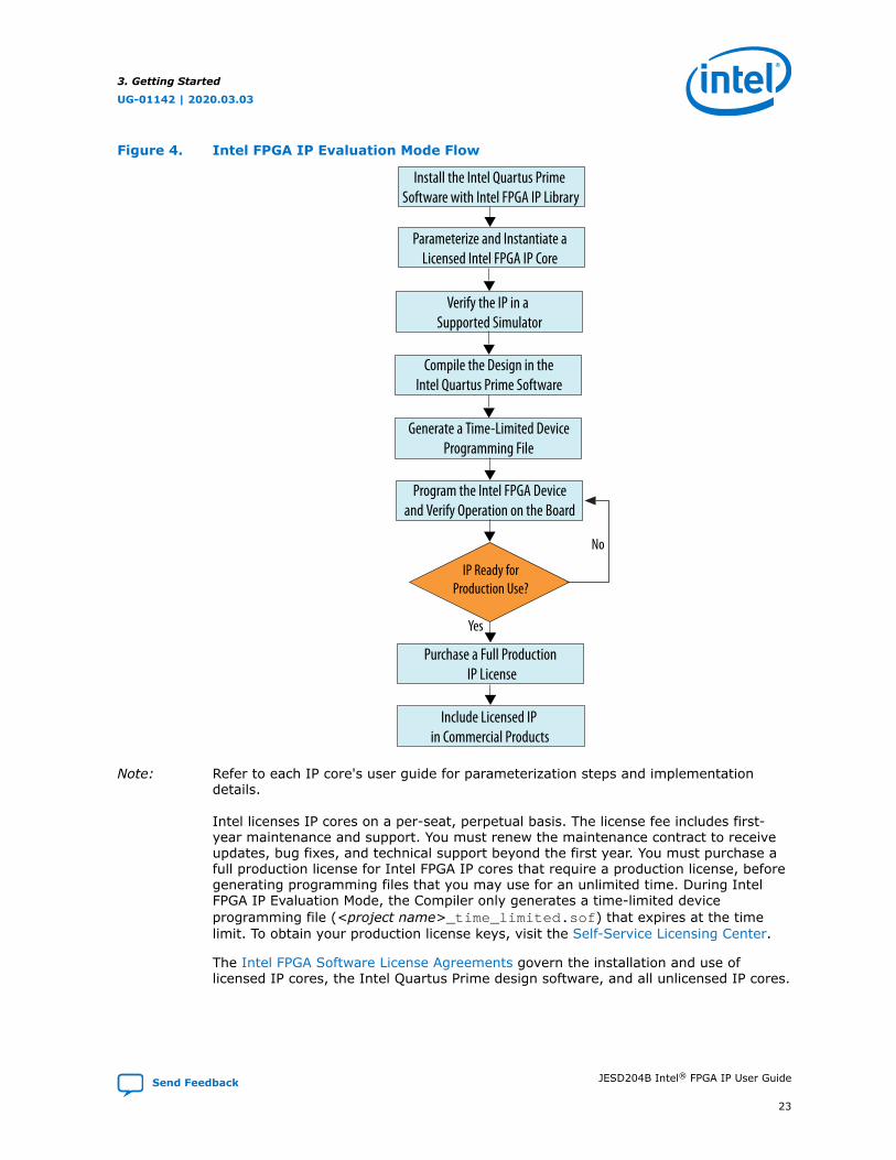
Figure 4. Intel FPGA IP Evaluation Mode Flow
Install the Intel Quartus Prime Software with Intel FPGA IP Library
Parameterize and Instantiate aLicensed Intel FPGA IP Core
Purchase a Full Production IP License
Verify the IP in a Supported Simulator
Compile the Design in theIntel Quartus Prime Software
Generate a Time-Limited DeviceProgramming File
Program the Intel FPGA Deviceand Verify Operation on the Board
No
Yes
IP Ready forProduction Use?
Include Licensed IP in Commercial Products
Note: Refer to each IP core's user guide for parameterization steps and implementationdetails.
Intel licenses IP cores on a per-seat, perpetual basis. The license fee includes first-year maintenance and support. You must renew the maintenance contract to receiveupdates, bug fixes, and technical support beyond the first year. You must purchase afull production license for Intel FPGA IP cores that require a production license, beforegenerating programming files that you may use for an unlimited time. During IntelFPGA IP Evaluation Mode, the Compiler only generates a time-limited deviceprogramming file (<project name>_time_limited.sof) that expires at the timelimit. To obtain your production license keys, visit the Self-Service Licensing Center.
The Intel FPGA Software License Agreements govern the installation and use oflicensed IP cores, the Intel Quartus Prime design software, and all unlicensed IP cores.
3. Getting Started
UG-01142 | 2020.03.03
Send Feedback JESD204B Intel® FPGA IP User Guide
23

Related Information
• Intel Quartus Prime Licensing Site
• Introduction to Intel FPGA Software Installation and Licensing
3.4. Upgrading IP Cores
Any Intel FPGA IP variations that you generate from a previous version or differentedition of the Intel Quartus Prime software, may require upgrade before compilation inthe current software edition or version. The Project Navigator displays a bannerindicating the IP upgrade status. Click Launch IP Upgrade Tool or Project ➤Upgrade IP Components to upgrade outdated IP cores.
Figure 5. IP Upgrade Alert in Project Navigator
Icons in the Upgrade IP Components dialog box indicate when IP upgrade isrequired, optional, or unsupported for an IP variation in the project. Upgrade IPvariations that require upgrade before compilation in the current version of the IntelQuartus Prime software.
3. Getting Started
UG-01142 | 2020.03.03
JESD204B Intel® FPGA IP User Guide Send Feedback
24
Note: Upgrading IP cores may append a unique identifier to the original IP core entitynames, without similarly modifying the IP instance name. There is no requirement toupdate these entity references in any supporting Intel Quartus Prime file, such as theIntel Quartus Prime Settings File (.qsf), Synopsys* Design Constraints File (.sdc),or Signal Tap File (.stp), if these files contain instance names. The Intel QuartusPrime software reads only the instance name and ignores the entity name in pathsthat specify both names. Use only instance names in assignments.
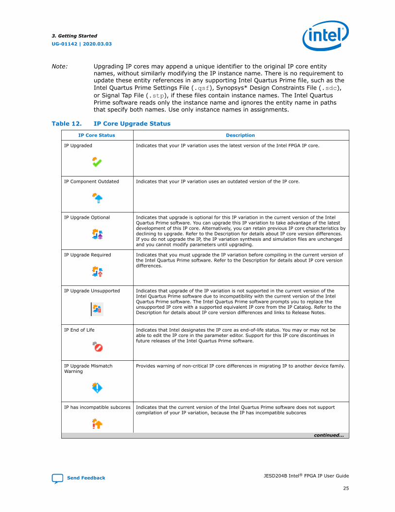
Table 12. IP Core Upgrade Status
IP Core Status Description
IP Upgraded
Indicates that your IP variation uses the latest version of the Intel FPGA IP core.
IP Component Outdated
Indicates that your IP variation uses an outdated version of the IP core.
IP Upgrade Optional
Indicates that upgrade is optional for this IP variation in the current version of the IntelQuartus Prime software. You can upgrade this IP variation to take advantage of the latestdevelopment of this IP core. Alternatively, you can retain previous IP core characteristics bydeclining to upgrade. Refer to the Description for details about IP core version differences.If you do not upgrade the IP, the IP variation synthesis and simulation files are unchangedand you cannot modify parameters until upgrading.
IP Upgrade Required
Indicates that you must upgrade the IP variation before compiling in the current version ofthe Intel Quartus Prime software. Refer to the Description for details about IP core versiondifferences.
IP Upgrade Unsupported
Indicates that upgrade of the IP variation is not supported in the current version of theIntel Quartus Prime software due to incompatibility with the current version of the IntelQuartus Prime software. The Intel Quartus Prime software prompts you to replace theunsupported IP core with a supported equivalent IP core from the IP Catalog. Refer to theDescription for details about IP core version differences and links to Release Notes.
IP End of Life
Indicates that Intel designates the IP core as end-of-life status. You may or may not beable to edit the IP core in the parameter editor. Support for this IP core discontinues infuture releases of the Intel Quartus Prime software.
IP Upgrade MismatchWarning
Provides warning of non-critical IP core differences in migrating IP to another device family.
IP has incompatible subcores
Indicates that the current version of the Intel Quartus Prime software does not supportcompilation of your IP variation, because the IP has incompatible subcores
continued...
3. Getting Started
UG-01142 | 2020.03.03
Send Feedback JESD204B Intel® FPGA IP User Guide
25

IP Core Status Description
Compilation of IP NotSupported
Indicates that the current version of the Intel Quartus Prime software does not supportcompilation of your IP variation. This can occur if another edition of the Intel Quartus Primesoftware, such as the Intel Quartus Prime Standard Edition, generated this IP. Replace thisIP component with a compatible component in the current edition.
Follow these steps to upgrade IP cores:
1. In the latest version of the Intel Quartus Prime software, open the Intel QuartusPrime project containing an outdated IP core variation. The Upgrade IPComponents dialog box automatically displays the status of IP cores in yourproject, along with instructions for upgrading each core. To access this dialog boxmanually, click Project ➤ Upgrade IP Components.
2. To upgrade one or more IP cores that support automatic upgrade, ensure that youturn on the Auto Upgrade option for the IP cores, and click Auto Upgrade. TheStatus and Version columns update when upgrade is complete. Example designsthat any Intel FPGA IP core provides regenerate automatically whenever youupgrade an IP core.
3. To manually upgrade an individual IP core, select the IP core and click Upgrade inEditor (or simply double-click the IP core name). The parameter editor opens,allowing you to adjust parameters and regenerate the latest version of the IP core.
3. Getting Started
UG-01142 | 2020.03.03
JESD204B Intel® FPGA IP User Guide Send Feedback
26
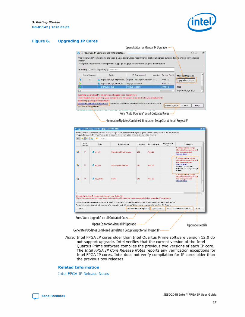
Figure 6. Upgrading IP Cores
Runs “Auto Upgrade” on all Outdated Cores
Opens Editor for Manual IP Upgrade
Generates/Updates Combined Simulation Setup Script for all Project IP
Runs “Auto Upgrade” on all Outdated Cores
Opens Editor for Manual IP Upgrade Upgrade DetailsGenerates/Updates Combined Simulation Setup Script for all Project IP
Note: Intel FPGA IP cores older than Intel Quartus Prime software version 12.0 donot support upgrade. Intel verifies that the current version of the IntelQuartus Prime software compiles the previous two versions of each IP core.The Intel FPGA IP Core Release Notes reports any verification exceptions forIntel FPGA IP cores. Intel does not verify compilation for IP cores older thanthe previous two releases.
Related Information
Intel FPGA IP Release Notes
3. Getting Started
UG-01142 | 2020.03.03
Send Feedback JESD204B Intel® FPGA IP User Guide
27

3.5. IP Catalog and Parameter Editor
The IP Catalog displays the IP cores available for your project, including Intel FPGA IPand other IP that you add to the IP Catalog search path. Use the following features ofthe IP Catalog to locate and customize an IP core:
• Filter IP Catalog to Show IP for active device family or Show IP for alldevice families. If you have no project open, select the Device Family in IPCatalog.
• Type in the Search field to locate any full or partial IP core name in IP Catalog.
• Right-click an IP core name in IP Catalog to display details about supporteddevices, to open the IP core's installation folder, and for links to IP documentation.
• Click Search for Partner IP to access partner IP information on the web.
The parameter editor prompts you to specify an IP variation name, optional ports, andoutput file generation options. The parameter editor generates a top-level IntelQuartus Prime IP file (.ip) for an IP variation in Intel Quartus Prime Pro Editionprojects or Quartus IP file (.qip) for an IP variation in Intel Quartus Prime StandardEdition projects.
3.6. Design Walkthrough
This walkthrough explains how to create a JESD204B IP core design using PlatformDesigner in the Intel Quartus Prime software. After you generate a custom variation ofthe JESD204B IP core, you can incorporate it into your overall project.
3.6.1. Creating a New Intel Quartus Prime Project
You can create a new Intel Quartus Prime project with the New Project Wizard.Creating a new project allows you to do the following:
• Specify the working directory for the project.
• Assign the project name.
• Designate the name of the top-level design entity.
1. Launch the Intel Quartus Prime software.
2. On the File menu, click New Project Wizard.
3. In the New Project Wizard: Directory, Name, Top-Level Entity page, specifythe working directory, project name, and top-level design entity name. Click Next.
4. In the New Project Wizard: Add Files page, select the existing design files (ifany) you want to include in the project.(14) Click Next.
(14) To include existing files, you must specify the directory path to where you installed theJESD204B IP core. You must also add the user libraries if you installed the IP core Library in adifferent directory from where you installed the Intel Quartus Prime software.
3. Getting Started
UG-01142 | 2020.03.03
JESD204B Intel® FPGA IP User Guide Send Feedback
28

5. In the New Project Wizard: Family & Device Settings page, select the devicefamily and specific device you want to target for compilation. Click Next.
6. In the EDA Tool Settings page, select the EDA tools you want to use with theIntel Quartus Prime software to develop your project.
7. Review the summary of your chosen settings in the New Project Wizard window,then click Finish to complete the Intel Quartus Prime project creation.
3.6.2. Parameterizing and Generating the IP
Refer to Table 15 on page 36 for the IP core parameter values and description.
1. In the IP Catalog (Tools ➤ IP Catalog), locate and double-click the JESD204BIntel FPGA IP.
2. Specify a top-level name for your custom IP variation. This name identifies the IPcore variation files in your project. If prompted, also specify the target Intel FPGAdevice family and output file HDL preference. Click OK.
3. In the Main tab, set the following options:
— Jesd204b wrapper
— Data path
— Jesd204b subclass
— Data Rate
— Transceiver Tile
— PCS Option
— PLL Type
— Bonding Mode
— PLL/CDR Reference Clock Frequency
— Enable Bit reversal and Byte reversal
— Enable Transceiver Dynamic Reconfiguration
— Enable Native PHY Debug Master Endpoint
— Enable Capability Registers
— Set user-defined IP identifier
— Enable Control and Status Registers
— Enable PRBS Soft Accumulators
4. In the Jesd204b Configurations tab, select the following configurations:
— Common configurations (L, M, Enable manual F configuration, F, N, N',S, K)
— Advanced configurations (SCR, CS, CF, HD, ECC_EN, PHADJ, ADJCNT,ADJDIR)
5. In the Configurations and Status Registers tab, set the following configurations:
— Device ID
— Bank ID
— Lane ID
— Lane checksum
3. Getting Started
UG-01142 | 2020.03.03
Send Feedback JESD204B Intel® FPGA IP User Guide
29

6. After parameterizing the core, go to the Example Design tab and click GenerateExample Design to create the simulation testbench. Skip to 8 if you do not wantto generate the design example.
7. Set a name for your <example_design_directory> and click OK to generatesupporting files and scripts.The testbench and scripts are located in the <example_design_directory>/ip_sim folder.
The Generate Example Design option generates supporting files for thefollowing entities:
• IP core for simulation—refer to Generating and Simulating the IP Testbench onpage 42
• IP core design example for simulation—refer to Generating and Simulating theDesign Example section in the respective design example user guides.
• IP core design example for synthesis—refer to Compiling the JESD204B IPCore Design Example section in the respective design example user guides.
8. Click Finish or Generate HDL to generate synthesis and other optional filesmatching your IP variation specifications. The parameter editor generates the top-level .ip, .qip or .qsys IP variation file and HDL files for synthesis andsimulation.
The top-level IP variation is added to the current Intel Quartus Prime project. ClickProject ➤ Add/Remove Files in Project to manually add a .qip or .qsys fileto a project. Make appropriate pin assignments to connect ports.
Note: Some parameter options are grayed out if they are not supported in a selectedconfiguration or it is a derived parameter.
Related Information
• Design Examples for JESD204B IP Core User GuideProvides information about design examples for Arria V, Cyclone V, Stratix V,and Intel Arria 10 devices using Intel Quartus Prime Standard Edition software.
• JESD204B Intel Arria 10 FPGA IP Design Example User Guide
• JESD204B Intel Stratix 10 FPGA IP Design Example User Guide
• JESD204B Intel Cyclone 10 GX FPGA IP Design Example User Guide
• JESD204B Intel Agilex FPGA IP Design Example User Guide
3.6.3. Compiling the JESD204B IP Core Design
Refer to the JESD204B IP Design Considerations on page 31 before compiling theJESD204B IP core design.
To compile your design, click Start Compilation on the Processing menu in the IntelQuartus Prime software. You can use the generated .ip or .qip file to includerelevant files into your project.
Related Information
• JESD204B IP Design Considerations on page 31
• Intel Quartus Prime HelpMore information about compilation in Intel Quartus Prime software.
3. Getting Started
UG-01142 | 2020.03.03
JESD204B Intel® FPGA IP User Guide Send Feedback
30

3.6.4. Programming an FPGA Device
After successfully compiling your design, program the targeted Intel device with theIntel Quartus Prime Programmer and verify the design in hardware. For instructions onprogramming the FPGA device, refer to the Device Programming section in the IntelQuartus Prime Handbook.
Related Information
Device Programming
3.7. JESD204B Design Examples
The JESD204B IP offers design examples that you can generate through the IP catalogin the Intel Quartus Prime software.
For detailed information about the JESD204B design examples, refer to following userguides:
Related Information
• Design Examples for JESD204B IP Core User GuideProvides information about design examples for Arria V, Cyclone V, Stratix V,and Intel Arria 10 devices using Intel Quartus Prime Standard Edition software.
• JESD204B Intel Arria 10 FPGA IP Design Example User Guide
• JESD204B Intel Stratix 10 FPGA IP Design Example User Guide
• JESD204B Intel Cyclone 10 GX FPGA IP Design Example User Guide
• JESD204B Intel Agilex FPGA IP Design Example User Guide
3.8. JESD204B IP Design Considerations
You must be aware of the following conditions when integrating the JESD204B IP inyour design:
• Integrating the IP in Platform Designer
• Pin assignments
• Adding external transceiver PLL
• Timing constraints for the input clock
3.8.1. Integrating the JESD204B IP in Platform Designer
You can integrate the JESD204B IP with other Platform Designer components withinPlatform Designer.
You can connect standard interfaces like clock, reset, Avalon-MM, Avalon-ST, HSSIbonded clock, HSSI serial clock, and interrupt interfaces within Platform Designer.However, for conduit interfaces, you are advised to export all those interfaces andhandle them outside of Platform Designer. (15) This is because conduit interfaces arenot part of the standard interfaces. Thus, there is no guarantee on compatibilitybetween different conduit interfaces.
3. Getting Started
UG-01142 | 2020.03.03
Send Feedback JESD204B Intel® FPGA IP User Guide
31

Note: The Transport Layer provided in this JESD204B IP design example is not supported inPlatform Designer. Therefore, you must export all interfaces that connect to theTransport Layer (for example, jesd204_tx_link interface) and connect them to atransport layer outside of Platform Designer.
Figure 7. Example of Connecting JESD204B IP with Other Platform DesignerComponents in Platform DesignerFigure shows an example of how you connect the IP with other Platform Designer components in PlatformDesigner.
Related Information
• Design Examples for JESD204B IP Core User GuideProvides information about design examples for Arria V, Cyclone V, Stratix V,and Intel Arria 10 devices using Intel Quartus Prime Standard Edition software.
• JESD204B Intel Arria 10 FPGA IP Design Example User Guide
• JESD204B Intel Stratix 10 FPGA IP Design Example User Guide
• JESD204B Intel Cyclone 10 GX FPGA IP Design Example User Guide
• JESD204B Intel Agilex FPGA IP Design Example User Guide
(15) You can also connect conduit interfaces within Platform Designer but you must create adaptercomponents to handle all the incompatibility issues like incompatible signal type and width.
3. Getting Started
UG-01142 | 2020.03.03
JESD204B Intel® FPGA IP User Guide Send Feedback
32

3.8.2. Pin Assignments
Set the pin assignments before you compile to provide direction to the Intel QuartusPrime software Fitter tool. You must also specify the signals that should be assigned todevice I/O pins.
You can create virtual pins to avoid making specific pin assignments for top-levelsignals. This is useful when you want to perform compilation, but are not ready tomap the design to hardware. Intel recommends that you create virtual pins for allunused top-level signals to improve timing closure.
Note: Do not create virtual pins for the clock or reset signals.
For Intel Agilex and Intel Stratix 10 E-tile devices, use the E-Tile Channel PlacementTool to get a valid pinout. Specify the transceiver mode as PMA direct - NRZ.
Related Information
E-Tile Channel Placement ToolFor E-tile devices, use the channel placement tool to assist you in making pinassignments.
3.8.3. Adding External Transceiver PLLs
The JESD204B IP core variations that target an Intel Stratix 10 L-tile, Intel Stratix 10H-tile, Intel Arria 10, or Intel Cyclone 10 GX FPGA device, require external transceiverPLLs for compilation. Select medium bandwidth for the PLL settings.
Note: For Intel Agilex and Intel Stratix 10 E-tile devices, the transceiver PLL is within thetransceiver itself; so the design does not require external PLLs.
JESD204B IP variations that target an Arria V, Cyclone V, or Stratix V FPGA devicecontain transceiver PLLs. Therefore, no external PLLs are required for compilation.
Intel recommends that you follow the PLL recommendations in the respectiveTransceiver PHY user guides based on the data rates.
Note: The PMA width is 20 bits for Hard PCS and 40 bits for Soft PCS.
Related Information
• V-Series Transceiver PHY User Guide
• Intel Arria 10 Transceiver PHY User Guide
• Intel Cyclone 10 GX Transceiver PHY User Guide
• Intel Stratix 10 L- and H-tile Transceiver PHY User Guide
• E-tile Transceiver PHY User Guide
3.8.4. Timing Constraints For Input Clocks
When you generate the JESD204B IP variation, the Intel Quartus Prime softwaregenerates a Synopsys Design Constraints File (.sdc) that specifies the timingconstraints for the input clocks to your IP.
3. Getting Started
UG-01142 | 2020.03.03
Send Feedback JESD204B Intel® FPGA IP User Guide
33

When you generate the JESD204B IP, your design is not yet complete and theJESD204B IP is not yet connected in the design. The final clock names and paths arenot yet known. Therefore, the Intel Quartus Prime software cannot incorporate thefinal signal names in the .sdc file that it automatically generates. Instead, you mustmanually modify the clock signal names in this file to integrate these constraints withthe timing constraints for your full design.
This section describes how to integrate the timing constraints that the Intel QuartusPrime software generates with your IP into the timing constraints for your design.
The Intel Quartus Prime software automatically generates the altera_jesd204.sdcfile that contains the JESD204B IP's timing constraints.
Three clocks are created at the input clock port:
• JESD204B TX IP:
— txlink_clk
— reconfig_to_xcvr[0] (for Arria V, Cyclone V, and Stratix V devices only)
— reconfig_clk (for Intel Arria 10, Intel Cyclone 10 GX, and Intel Stratix 10devices only)
— tx_avs_clk
• JESD204B RX IP:
— rxlink_clk
— reconfig_to_xcvr[0] (for Arria V, Cyclone V, and Stratix V devices only)
— reconfig_clk (for Intel Arria 10, Intel Cyclone 10 GX, and Intel Stratix 10devices only)
— rx_avs_clk
In a functional system design, these clocks (except for reconfig_to_xcvr[0] clock)are typically provided by the core PLL.
In the .sdc file for your project, make the following command changes:
• Specify the PLL clock reference pin frequency using the create_clock command.
• Derive the PLL generated output clocks from the PLL Intel FPGA IP (for Arria V,Cyclone V and Stratix V) or IOPLL Intel FPGA IP (for Intel Arria 10 and IntelCyclone 10 GX) using the derive_pll_clocks command.
• For Intel Stratix 10 devices, Intel FPGA IOPLL IP core has SDC file which derivesthe PLL clocks based on your PLL configurations. You need not add thederive_pll_clocks command into your top level SDC file."
• Comment out the create_clock commands for the txlink_clk,reconfig_to_xcvr[0] or reconfig_clk, and tx_avs_clk, rxlink_clk,and rx_avs_clk clocks in the altera_jesd204.sdc file.
• Identify the base and generated clock name that correlates to the txlink_clk,reconfig_clk, and tx_avs_clk, rxlink_clk, and rx_avs_clk clocks usingthe report_clock command.
• Describe the relationship between base and generated clocks in the design usingthe set_clock_groups command.
3. Getting Started
UG-01142 | 2020.03.03
JESD204B Intel® FPGA IP User Guide Send Feedback
34

After you complete your design, you must modify the clock names in your .sdc file tothe full-design clock names, taking into account both the IP instance name in the fulldesign, and the design hierarchy. Be careful when adding the timing exceptions basedon your design, for example, when the JESD204B IP handles asynchronous timingbetween the txlink_clk, rxlink_clk, pll_ref_clk, tx_avs_clk, rx_avs_clk,and reconfig_clk (for Intel Arria 10, Intel Cyclone 10 GX, and Intel Stratix 10 only)clocks.
The table below shows an example of clock names in the altera_jesd204.sdc andinput clock names in the user design. In this example, there is a dedicated input clockfor the transceiver TX PLL and CDR at the refclk pin. The device_clk is the inputto the core PLL clkin pin. The IP and transceiver Avalon-MM interfaces have separateexternal clock sources with different frequencies.
Table 13. Example A
Original clocknames in
altera_jesd204.sdc
User design inputclock names
Frequency(MHz)
Recommended SDC timing constraint
tx_pll_ref_clk xcvr_tx_rx_refclk 250 create_clock -name xcvr_tx_rx_refclk -period 4.0 [get_portsxcvr_tx_rx_refclk ]create_clock -name device_clk -period 8.0 [get_portsdevice_clk]create_clock -name jesd204_avs_clk -period 10.0 [get_portsjesd204_avs_clk]create_clock -name phy_mgmt_clk -period 13.3 [get_portsphy_mgmt_clk]derive_pll_clocksset_clock_groups -asynchronous \-group {xcvr_tx_rx_refclk \<base and generated clock names as reported by report_clockcommands> \} \-group {device_clk \<base and generated clock names as reported by report_clockcommands> \} \-group {jesd204_avs_clk} \-group {phy_mgmt_clk \<base and generated clock names as reported by report_clockcommands> \}
rx_pll_ref_clk
txlink_clk device_clk 125
rxlink_clk
tx_avs_clk jesd204_avs_clk 100
rx_avs_clk
reconfig_clk (16) phy_mgmt_clk 75
However, if your design requires you to connect the rx_avs_clk and reconfig_clkto the same clock, you need to put them in the same clock group.
The table below shows an example where the device_clk in this design is an inputinto the transceiver refclk pin. The IP's Avalon-MM interface shares the same clocksource as the transceiver management clock.
(16) For Intel Arria 10, Intel Cyclone 10 GX, and Intel Stratix 10 only.
3. Getting Started
UG-01142 | 2020.03.03
Send Feedback JESD204B Intel® FPGA IP User Guide
35

Table 14. Example B
Original clocknames in
altera_jesd204.sdc
User design inputclock names
Frequency(MHz)
Recommended SDC timing constraint
tx_pll_ref_clk device_clk 125 create_clock -name device_clk -period 8.0 [get_portsdevice_clk]create_clock -name mgmt_clk -period 10.0 [get_portsmgmt_clk]derive_pll_clocksset_clock_groups -asynchronous \-group {device_clk \<base and generated clock names as reported by report_clockcommands> \} \-group {mgmt_clk \<base and generated clock names as reported by report_clockcommands> \}
rx_pll_ref_clk
txlink_clk
rxlink_clk
tx_avs_clk mgmt_clk 100
rx_avs_clk
reconfig_clk (17)
3.9. JESD204B Intel FPGA IP Parameters
Table 15. JESD204B Intel FPGA IP Parameters
Parameter Value Description
Main Tab
Device Family • Intel Agilex• Intel Stratix
10• Intel Arria 10• Intel Cyclone
10 GX• Stratix V• Cyclone V• Arria V• Arria V GZ
The targeted device family.
JESD204B Wrapper • Base Only• PHY Only• Both Base and
PHY
Select the JESD204B wrapper.• Base Only—generates the DLL only.• PHY Only—generates the transceiver PHY layer only (soft and hard
PCS).• Both Base and PHY—generates both DLL and transceiver PHY layers.
Data Path • Receiver• Transmitter• Duplex
Select the operation modes. This selection enables or disables thereceiver and transmitter supporting logic.• RX—instantiates the receiver to interface to the ADC.• TX—instantiates the transmitter to interface to the DAC.• Duplex—instantiates the receiver and transmitter to interface to
both the ADC and DAC.
JESD204B Subclass • 0• 1• 2
Select the JESD204B subclass modes.• 0—Set subclass 0• 1—Set subclass 1• 2—Set subclass 2
continued...
(17) For Intel Agilex, Intel Stratix 10, Intel Cyclone 10 GX, and Intel Arria 10 only.
3. Getting Started
UG-01142 | 2020.03.03
JESD204B Intel® FPGA IP User Guide Send Feedback
36

Parameter Value Description
Data Rate 1.0–19.2 Set the data rate for each lane.• Intel Agilex (E-tile)—2.0 Gbps to 19.2 Gbps• Intel Stratix 10 (L-tile, H-tile, and E-tile)—2.0 Gbps to 16.0 Gbps• Intel Cyclone 10 GX—2.0 Gbps to 6.25 Gbps• Intel Arria 10—2.0 Gbps to 15.0 Gbps• Stratix V—2.0 Gbps to 12.5 Gbps• Cyclone V—1.0 Gbps to 5.0 Gbps• Arria V—1.0 Gbps to 7.5 Gbps• Arria V GZ—2.0 Gbps to 9.9 GbpsNote: The maximum data rate is limited due to different device speed
grades, transceiver PMA speed grades, and PCS options. Refer to Performance and Resource Utilization on page 14 for themaximum data rate support.
Transceiver Tile • E-tile• H-tile
This option is available only when you target an Intel Stratix 10 devicethat supports both H-tile and E-tile. Select the transceiver tile you wantfor your design.When you select E-tile, you can only use soft PCS.Note: For simplex variants with E-tile transceiver, the underneath
transceiver is in duplex mode. The merging of independent TXand RX within a transceiver channel is not supported in thisversion.
PCS Option • Enabled HardPCS
• Enabled SoftPCS
• Enabled PMADirect
Select the PCS modes.• Enabled Hard PCS—use Hard PCS components. Select this option to
minimize resource utilization with data rate that supports up to thelimitation of the Hard PCS.Note: For this setting, use 8G PCS mode with 20 bits PMA width
and 32-bit PCS width.• Enabled Soft PCS—use Soft PCS components. Select this option to
allow higher supported data rate but increases the resourceutilization. This option is applicable for all devices except Cyclone Vand Arria V GT/ST.Note: For this setting, use 10G PCS mode with 40 bits PMA width
and 40 bits PCS width.• Enabled PMA Direct—Native PHY is set to PMA Direct mode. Select
this option to allow the highest supported data rate and to maximizethe resource utilization. This option is applicable only forArria V GT/ST devices.Note: For this setting, use PMA Direct mode with 80-bit PMA width.
PLL Type • CMU• ATX
Select the phase-locked loop (PLL) types, depending on the FPGA devicefamily. This parameter is not applicable to Intel Arria 10, Intel Cyclone10 GX, and Intel Stratix 10 devices.• Cyclone V—CMU• Arria V—CMU• Stratix V—CMU, ATX
Bonding Mode • Bonded• Non-bonded
Select the bonding modes.• Bonded—select this option to minimize inter-lanes skew for the
transmitter datapath.• Non-bonded—select this option to disable inter-lanes skew control
for the transmitter datapath.Note: For Stratix V, Arria V, and Cyclone V devices, the bonding type is
automatically selected based on the device family and number oflanes that you set.
continued...
3. Getting Started
UG-01142 | 2020.03.03
Send Feedback JESD204B Intel® FPGA IP User Guide
37

Parameter Value Description
PLL/CDR Reference ClockFrequency
Variable Set the transceiver reference clock frequency for PLL or CDR.• For Stratix V, Arria V, and Cyclone V devices, the frequency range
available for you to choose depends on the PLL type and data ratethat you select.
• For Intel Agilex, Intel Stratix 10, Intel Cyclone 10 GX, and Intel Arria10 devices, the frequency range available for you to choose dependson the data rate.
VCCR_GXB and VCCT_GXBSupply Voltage for theTransceiver
• 1.1V• 1.0V
Select the supply voltage for the transceiver.For details about the minimum, typical, and maximum supply voltagespecifications, refer to the Intel Stratix 10 Device Datasheet.Note: Available only for Intel Stratix 10 L-tile and H-tile devices.
Enable Bit reversal andByte reversal
On, Off The JESD204B IP uses four 10-bit symbols (denoted as symbol3,symbol2, symbol1, and symbol0) for the 8B/10B encoding scheme.Symbol0 is the first symbol to be shifted out through the serial linkwhile symbol3 is the last symbol to be shifted out.• Turn off this option to set the data transmission order to start from
the least significant bit (lsb) of each symbol. For example,symbol0[0] is shifted out first, followed by symbol0[1], and so onuntil the entire symbol0 is shifted out. The transmission continueswith symbol1[0] through symbol3[9].
• Turn on this option to set the data transmission order to start fromthe most significant bit (lsb) of each symbol. For example,symbol0[9] is shifted out first, followed by symbol0[8], and so onuntil the entire symbol0 is shifted out. The transmission continueswith symbol1[9] through symbol3[0].
Enable Transceiver DynamicReconfiguration
On, Off Turn on this option to enable dynamic data rate change. For V seriesdevices, when you enable this option, you need to connect thereconfiguration interface to the transceiver reconfiguration controller.(18)
For Intel Arria 10, Intel Cyclone 10 GX, and Intel Stratix 10 devices,turn on this option to enable the Transceiver Native PHY reconfigurationinterface.
Enable Native PHY DebugMaster Endpoint (19)
On, Off Turn on this option for the Transceiver Native PHY IP core to include anembedded Native PHY Debug Master Endpoint. This block connectsinternally to the Avalon-MM slave interface of the Transceiver NativePHY and can access the reconfiguration space of the transceiver. It canperform certain test and debug functions via JTAG using SystemConsole.This parameter is valid only when you turn on the Enable TransceiverDynamic Reconfiguration parameter.Note: Available only for Intel Agilex, Intel Stratix 10, Intel Cyclone 10
GX, and Intel Arria 10 devices.
Share ReconfigurationInterface (19)
On, Off When enabled, Transceiver Native PHY presents a single Avalon-MMslave interface for dynamic reconfiguration of all channels. In thisconfiguration the upper address bits (Intel Stratix 10: [log2<L>+10:11]; Intel Arria 10/Intel Cyclone 10 GX: [log2<L>+9:10]) of thereconfiguration address bus specify the selected channel. The upperaddress bits only exist when L>1. Address bits (Intel Stratix 10: [10:0];Intel Arria 10/Intel Cyclone 10 GX: [9:0]) provide the register offsetaddress within the reconfiguration space of the selected channel. L isthe number of channel.
continued...
(18) To perform dynamic reconfiguration, you have to instantiate the Transceiver ReconfigurationController from the IP Catalog and connect it to the JESD204B IP core through thereconfig_to_xcvr and reconfig_from_xcvr interface.
(19) To support the Transceiver Toolkit in your design, you must turn on this option.
3. Getting Started
UG-01142 | 2020.03.03
JESD204B Intel® FPGA IP User Guide Send Feedback
38

Parameter Value Description
When disabled, the Native PHY IP core provides an independentreconfiguration interface for each channel. For example, when areconfiguration interface is not shared for a four-channel Native PHY IPinstance, reconfig_address[9:0] corresponds to thereconfiguration address bus of logical channel 0,reconfig_address[19:10] correspond to the reconfigurationaddress bus of logical channel 1, reconfig_address[29:20]corresponds to the reconfiguration address bus of logical channel 2, andreconfig_address[39:30] correspond to the reconfigurationaddress bus of logical channel 3.For configurations using more than one channel, this option must beenabled when you turn on Enable Native PHY Debug MasterEndpoint.Note: Available only for Intel Agilex, Intel Stratix 10, Intel Cyclone 10
GX, and Intel Arria 10 devices.
Provide SeparateReconfiguration Interfacefor Each Channel
On, Off When enabled, transceiver dynamic reconfiguration interface presentsseparate clock, reset, and Avalon-MM slave interface for each channelinstead of a single wide bus. This option is only available when ShareReconfiguration Interface is turned off.Note: Available in Intel Quartus Prime Pro Edition only.
Enable CapabilityRegisters (19)
On, Off Turn on this option to enable capability registers, which provides highlevel information about the transceiver channel's configuration.Note: Available only for Intel Agilex, Intel Stratix 10, Intel Cyclone 10
GX, and Intel Arria 10 devices.
Set user-defined IPidentifier
0–255 Set a user-defined numeric identifier that can be read from the useridentifier offset when you turn on the Enable CapabilityRegisters parameter.Note: Available only for Intel Agilex, Intel Stratix 10, Intel Cyclone 10
GX, and Intel Arria 10 devices.
Enable Control and StatusRegisters (19)
On, Off Turn on this option to enable soft registers for reading status signalsand writing control signals on the PHY interface through the embeddeddebug. For more information, refer to the respective Transceiver UserGuides.Note: Available only for Intel Agilex, Intel Stratix 10, Intel Cyclone 10
GX, and Intel Arria 10 devices.
Enable PRBS SoftAccumulators (19)
On, Off Turn on this option to set the soft logic to perform pseudorandom binarysequence (PRBS) bit and error accumulation when using the hard PRBSgenerator and checker.Note: Available only for Intel Agilex, Intel Stratix 10, Intel Cyclone 10
GX, and Intel Arria 10 devices.
JESD204B Configurations Tab
Lanes per converter device (L) 1–8 Set the number of lanes per converter device.Note: Refer to Performance and Resource Utilization on page 14
for the common supported range for L and the resourceutilization.
Converters per device (M) 1–256 Set the number of converters per converter device.
Enable manual F configuration On, Off Turn on this option to set parameter F in manual mode and enablethis parameter to be configurable. Otherwise, the parameter F is inderived mode.You have to enable this parameter and configure the appropriate Fvalue if the transport layer in your design is supporting ControlWord (CF) or High Density format(HD), or both.
continued...
3. Getting Started
UG-01142 | 2020.03.03
Send Feedback JESD204B Intel® FPGA IP User Guide
39

Note: The auto derived F value using formula F=M*S*N\'/(8*L)may not apply if parameter CF or parameter HD, or bothare enabled.
Octets per frame (F) • 1–256 (forIntel Stratix 10devices only)
• 1, 2, 4–256(for non IntelStratix 10devices)
The number of octets per frame is derived from F= M*N'*S/(8*L).
Converter resolution (N) 1–32 Set the number of conversion bits per converter.
Transmitted bits per sample (N') 1–32 Set the number of transmitted bits per sample (JESD204 wordsize, which is in nibble group).Note: If parameter CF equals to 0 (no control word), parameter N'
must be larger than or equal to sum of parameter N andparameter CS (N' ≥ N + CS). Otherwise, parameter N' mustbe larger than or equal to parameter N (N'≥N).
Samples per converter perframe (S)
1–32 Set the number of transmitted samples per converter per frame.
Frames per multiframe (K) 1–32 Set the number of frames per multiframe. This value is dependenton the value of F and is derived using the following constraints:• The value of K must fall within the range of 17/F <= K <=
min(32, floor (1024/F))• The value of F*K must be divisible by 4
Enable scramble (SCR) On, Off Turn on this option to scramble the transmitted data or descramblethe receiving data.
Control Bits (CS) 0–3 Set the number of control bits per conversion sample.
Control Words (CF) 0–32 Set the number of control words per frame clock period per link.
High density user data format(HD)
On, Off Turn on this option to set the data format. This parameter controlswhether a sample may be divided over more lanes.• On: High Density format• Off: Data should not cross the lane boundary
Enable Error Code Correction(ECC_EN)
On, Off Turn on this option to enable error code correction (ECC) formemory blocks.
Phase adjustment request(PHADJ)
On, Off Turn on this option to specify the phase adjustment request to theDAC.• On: Request for phase adjustment• Off: No phase adjustmentThis parameter is valid for Subclass 2 mode only.
Adjustment resolution stepcount (ADJCNT)
0–15 Set the adjustment resolution for the DAC LMFC.This parameter is valid for Subclass 2 mode only.
Direction of adjustment(ADJDIR)
• Advance• Delay
Select to adjust the DAC LMFC direction.This parameter is valid for Subclass 2 mode only.
Configurations and Status Registers Tab
Device ID 0–255 Set the device ID number.
Bank ID 0–15 Set the device bank ID number.
Lane# ID 0–31 Set the lane ID number.
Lane# checksum 0–255 Set the checksum for each lane ID.
3. Getting Started
UG-01142 | 2020.03.03
JESD204B Intel® FPGA IP User Guide Send Feedback
40

Note: The PMA Adaptation parameters are available only for Intel Agilex and Intel Stratix10 E-tile devices. For more information about the PMA Adaptation parameters, referto the PMA Adaptation section in the E-tile Transceiver PHY User Guide.
Related Information
• E-tile Transceiver PHY User Guide
• Performance and Resource Utilization on page 14
3.10. JESD204B IP Component Files
The following table describes the generated files and other files that may be in yourproject directory. The names and types of generated files specified may varydepending on whether you create your design with VHDL or Verilog HDL.
Table 16. Generated Files
Extension Description
<variation name>.v or .vhd IP variation file, which defines a VHDL or Verilog HDL description of the custom IP.Instantiate the entity defined by this file inside of your design. Include this file whencompiling your design in the Intel Quartus Prime software.
<variation name>.cmp A VHDL component declaration file for the IP variation. Add the contents of this file toany VHDL architecture that instantiates the IP.
<variation name>.sdc Contains timing constraints for your IP variation.
<variation name>.qip or .ip Contains Intel Quartus Prime project information for your IP variation.
<variation name>.tcl Tcl script file to run in Intel Quartus Prime software.
<variation name>.sip Contains IP library mapping information required by the Intel Quartus Primesoftware.The Intel Quartus Prime software generates a . sip file during generation ofsome Intel FPGA IPs. You must add any generated .sip file to your project for use byNativeLink simulation and the Intel Quartus Prime Archiver.
<variation name>.spd Contains a list of required simulation files for your IP.
3.11. JESD204B IP Testbench
The JESD204B IP includes a testbench to demonstrate a normal link-up sequence forthe JESD204B IP with a supported configuration. The testbench also provides anexample of how to control the JESD204B IP interfaces.
The testbench instantiates the JESD204B IP in duplex mode and connects with theIntel FPGA Transceiver PHY Reset Controller IP. Some configurations are preset andare not programmable in the JESD204B IP testbench. For example, the JESD204B IPalways instantiates in duplex mode even if RX or TX mode is selected in the JESD204Bparameter editor.
Table 17. Preset Configurations for JESD204B IP Testbench
Configuration Preset Value
JESD204B Wrapper Base and PHY (MAC and PHY)
Data Path Simplex TX and simplex RX
PLL/CDR Reference Clock Frequency(20) For Base only, or Simplex TX variants:
continued...
3. Getting Started
UG-01142 | 2020.03.03
Send Feedback JESD204B Intel® FPGA IP User Guide
41

Configuration Preset Value
• Data_rate/20 (if you turn on Enabled Hard PCS)• Data_rate/40 (if you turn on Enabled Soft PCS)• Data_rate/80 (if you turn on Enabled PMA Direct)
Link Clock • Data_rate/40
AVS Clock 100 MHz
Figure 8. JESD204B IP Testbench Block DiagramThe external ATX PLL is present only in the JESD204B IP testbench targeting Intel Arria 10, Intel Cyclone 10GX, and Intel Stratix 10 L-tile and H-tile devices. For Intel Agilex and Intel Stratix 10 E-tile devices, theTransceiver PHY Reset Controller is within the transceiver block.
Packet
ATX PLL
Transceiver PHY ResetController IP Core
JESD204BIP Core
(TX)
PacketGenerator
PacketChecker
ReferenceClock
Generator
Link ClockGenerator
AVS ClockGenerator
Transceiver PHY ResetController IP Core
JESD204BIP Core
(RX)
JESD204B Testbench
3.11.1. Generating and Simulating the IP Testbench
You can simulate your JESD204B IP variation by using the provided IP demonstrationtestbench.
To use the JESD204B IP testbench, follow these steps:
1. Generate the simulation model. Refer to Generating the Testbench SimulationModel on page 43.
2. Simulate the testbench using the simulator-specific scripts that you havegenerated. Refer to Simulating the IP Testbench on page 43.
(20) For the ATX PLL supported range of reference clock frequencies, refer to the respective devicedatasheet.
3. Getting Started
UG-01142 | 2020.03.03
JESD204B Intel® FPGA IP User Guide Send Feedback
42

Note: Some configurations are preset and are not programmable in the JESD204B IPtestbench. For more details, refer to JESD204B IP Testbench on page 41 or theREADME.txt file located in the <example_design_directory>/ip_sim folder.
3.11.1.1. Generating the Testbench Simulation Model
To generate the testbench simulation model, execute the generated script(gen_sim_verilog.tcl or gen_sim_vhdl.tcl) located in the<example_design_directory>/ip_sim folder.
To run the Tcl script using the Intel Quartus Prime software, follow these steps:
1. Launch the Intel Quartus Prime software.
2. On the View menu, click Utility Windows ➤ Tcl Console.
3. In the Tcl Console, type cd <example_design_directory>/ip_sim to go tothe specified directory.
4. Type source gen_sim_verilog.tcl (Verilog) or source gen_sim_vhdl.tcl(VHDL) to generate the simulation files.
To run the Tcl script using the command line, follow these steps:
1. Obtain the Intel Quartus Prime software resource.
2. Type cd <example_design_directory>/ip_sim to go to the specifieddirectory.
3. Type quartus_sh -t gen_sim_verilog.tcl (Verilog) or quartus_sh -tgen_sim_vhdl.tcl (VHDL) to generate the simulation files.
3.11.1.2. Simulating the IP Testbench
Note: VHDL is not supported in VCS simulator.
Table 18. Simulation Setup Scripts
Simulator File Directory Script
ModelSim - Intel FPGAEdition/ModelSim - IntelFPGA Starter Edition
<example_design_directory>/ip_sim/testbench/setup_scripts/mentor
msim_setup.tcl
Synopsys VCS simulator <example_design_directory>/ip_sim/testbench/setup_scripts/synopsys/vcs
vcs_setup.sh
Synopsys VCS-MXsimulator
<example_design_directory>/ip_sim/testbench/setup_scripts/synopsys/vcsmx
vcsmx_setup.shsynopsys_sim.setup
Aldec Riviera-PRONote: Intel Agilex and
Intel Stratix 10 E-tile devices do notsupport thissimulator.
<example_design_directory>/ip_sim/testbench/setup_scripts/aldec
rivierapro_setup.tcl
Cadence NCSim <example_design_directory>/ip_sim/testbench/setup_scripts/cadence
ncsim_setup.sh
Cadence Xcelium Parallelsimulator
<example_design_directory>/ip_sim/testbench/setup_scripts/xcelium
xcelium_setup.sh
3. Getting Started
UG-01142 | 2020.03.03
Send Feedback JESD204B Intel® FPGA IP User Guide
43

Table 19. Simulation Run Scripts
Simulator File Directory Script
ModelSim - Intel FPGAEdition/ModelSim - IntelFPGA Starter Edition
<example_design_directory>/ip_sim/testbench/mentor run_altera_jesd204_tb.tcl
Synopsys VCS simulator <example_design_directory>/ip_sim/testbench/synopsys/vcs
run_altera_jesd204_tb.sh
Synopsys VCS-MXsimulator
<example_design_directory>/ip_sim/testbench/synopsys/vcsmx
run_altera_jesd204_tb.sh
Aldec Riviera-PRONote: Intel Agilex and
Intel Stratix 10 E-tile devices do notsupport thissimulator.
<example_design_directory>/ip_sim/testbench/aldec run_altera_jesd204_tb.tcl
Cadence NCSim <example_design_directory>/ip_sim/testbench/cadence run_altera_jesd204_tb.sh
Cadence Xcelium Parallelsimulator
<example_design_directory>/ip_sim/testbench/xcelium run_altera_jesd204_tb.sh
To simulate the testbench design using the ModelSim - Intel FPGA Edition/ModelSim -Intel FPGA Starter Edition, follow these steps:
1. Launch the ModelSim - Intel FPGA Edition/ModelSim - Intel FPGA Starter Edition.
2. On the File menu, click Change Directory ➤ Select<example_design_directory>/ip_sim/testbench/<simulator name>.
3. On the File menu, click Load ➤ Macro file. Select run_altera_jesd204_tb.tcl.This file compiles the design and runs the simulation automatically, providing apass/fail indication on completion.
To simulate the testbench design using the Aldec Riviera-PRO simulator, follow thesesteps:
1. Launch the Aldec Riviera-PRO simulator.
2. On the File menu, click Change Directory ➤ Select<example_design_directory>/ip_sim/testbench/<simulator name>.
3. On the Tool menu, click Execute Macro. Select run_altera_jesd204_tb.tcl.This file compiles the design and runs the simulation automatically, providing apass/fail indication on completion.
To simulate the testbench design using the VCS, VCS MX (in Linux), or Cadencesimulators, follow these steps:
1. Launch the Synopsys VCS or VCS-MX, or Cadence NCSim or Xcelium Parallelsimulator.
2. On the File menu, click Change Directory ➤ Select<example_design_directory>/ip_sim/testbench/<simulator name>.
3. Run the run_altera_jesd204_tb.sh file. This file compiles the design and runsthe simulation automatically, providing a pass/fail indication on completion.
3. Getting Started
UG-01142 | 2020.03.03
JESD204B Intel® FPGA IP User Guide Send Feedback
44

Related Information
Simulating Intel FPGA DesignsMore information about Intel FPGA simulation models.
3.11.2. Testbench Simulation Flow
The JESD204B testbench simulation flow:
1. At the start, the system is under reset (all the components are in reset).
2. After 100 ns, the Transceiver Reset Controller IP core power up and wait for thetx_ready and rx_ready signal from the Transceiver Reset Controller IP toassert.
3. After 500 ns (all devices except Intel Agilex and Intel Stratix 10 E-tile) or 1500 ns(Intel Agilex and Intel Stratix 10 E-tile devices), the reset signal of the JESD204BTX Avalon-MM interface is released (go HIGH). At the next positive edge of thelink_clk signal, the JESD204B TX link powers up by releasing its reset signal.
4. The JESD204B TX link starts transmitting K28.5 characters.
5. The reset signal of the JESD204B RX Avalon-MM interface is released (go HIGH).At the next positive edge of the link_clk signal, the JESD204B RX link powersup by releasing its reset signal.
6. Once the link is out of reset, a SYSREF pulse is generated to reset the LMFCcounter inside both the JESD204B TX and RX IP core.
7. When the txlink_ready signal is asserted, the packet generator starts sendingpackets to the TX datapath.
8. The packet checker starts comparing the packet sent from the TX datapath andreceived at the RX datapath after the rxlink_valid signal is asserted.
9. The testbench reports a pass or fail when all the packets are received andcompared.
The testbench concludes by checking that all the packets have been received.
If no error is detected, the testbench issues a TESTBENCH PASSED message statingthat the simulation was successful. If an error is detected, the testbench issues aTESTBENCH FAILED message to indicate that the testbench has failed.
Note: For Intel Stratix 10 L-tile and H-tile devices, reset deassertion staggering of TX/RXanalog and digital reset happens before the assertion of TX/RX ready. The resetstaggering may incur long simulation time. You may observe the staggering of TX andRX reset through tx_analogreset_stat, tx_digitalreset_stat,rx_analogreset_stat, and rx_digitalreset_stat respectively.
3. Getting Started
UG-01142 | 2020.03.03
Send Feedback JESD204B Intel® FPGA IP User Guide
45

4. JESD204B IP Functional DescriptionThe JESD204B IP implements a transmitter (TX) and receiver (RX) block. Each blockhas two layers and consists of the following components:
• Media access control (MAC)—DLL block that consists of the link layer (link statemachine and character replacement), CSR, Subclass 1 and 2 deterministic latency,scrambler or descrambler, and multiframe counter.
• Physical layer (PHY)—PCS and PMA block that consists of the 8B/10B encoder,word aligner, serializer, and deserializer.
You can specify the datapath and wrapper for your design and generate themseparately.
The TX and RX blocks in the DLL utilizes the Avalon-ST interface to transmit or receivedata and the Avalon-MM interface to access the CSRs. The TX and RX blocks operateon 32-bit data width per channel, where the frame assembly packs the data into fouroctets per channel. Multiple TX and RX blocks can share the clock and reset if the linkrates are the same.
Figure 9. Overview of the JESD204B IP Block DiagramIf your design uses hard PCS, the 8B/10B and word aligner blocks should be hard logic, but if your design usessoft PCS, the 8B/10B and word aligner blocks are soft logic.
RX Driver
TX Driver
Deserializer
SerializerFrame/Lane
AlignmentCharacter
Generation
Descrambler
ScramblerData Frame Assembly
Data Frame Deassembly
SYSREF
Frame Clock
ADC ApplicationLayer
DAC ApplicationLayer
Transport Layer Data Link Layer Physical Layer
Word Aligner
Soft Logic Hard Logic
JESD204B IP CoreJESD204BDesign Example
jesd204_tx_topMAC (jesd204_tx_base)
MAC (jesd204_rx_base) PHY (jesd204_rx_phy)
PHY (jesd204_tx_phy)
jesd204_rx_top
8B/10BEncoder
8B/10BDecoder
SYNC~
SYNC~
Frame/LaneAlignment
Character Buffer/Replace/Monitor
UG-01142 | 2020.03.03
Send Feedback
Intel Corporation. All rights reserved. Agilex, Altera, Arria, Cyclone, Enpirion, Intel, the Intel logo, MAX, Nios,Quartus and Stratix words and logos are trademarks of Intel Corporation or its subsidiaries in the U.S. and/orother countries. Intel warrants performance of its FPGA and semiconductor products to current specifications inaccordance with Intel's standard warranty, but reserves the right to make changes to any products and servicesat any time without notice. Intel assumes no responsibility or liability arising out of the application or use of anyinformation, product, or service described herein except as expressly agreed to in writing by Intel. Intelcustomers are advised to obtain the latest version of device specifications before relying on any publishedinformation and before placing orders for products or services.*Other names and brands may be claimed as the property of others.
ISO9001:2015Registered

Figure 10. JESD204B IP TX and RX Datapath Block Diagram
The JESD204B IP uses the Avalon-ST source and sink interfaces, with unidirectional flow of data, to transmitand receive data on the FPGA fabric interface.
TX FrameAssembly
Per Device
TX CSRPer Device
TX CTLPer Device
Scrambler Data LinkLayer (TX)
SoftPCS(TX)
Hard PCSand
TransceiverJESD204B(TX) Per Device
CSR
CSR
CSR
32 Bit PCSPer Channel
Transceiver (Duplex)Per Device
SYNC_NSYSREFTX_INTTXLINK_CLKTXFRAME_CLK
Avalon-MM
Avalon-ST
To AvalonInterface
Bus
RX FrameDeassemblyPer Device
RX CSRPer Device
RX CTLPer Device
Descrambler Data LinkLayer (RX)
SoftPCS(RX)
Hard PCSand
TransceiverJESD204B(RX) Per Device
CSR
CSR
CSR CSR
CSR
32 Bit PCSPer Channel
32/40/80PCS
SYNC_NSYSREFRX_INTRXLINK_CLKRXFRAME_CLK
Avalon-MM
Avalon-ST
To AvalonInterface
Bus
JESD204B TX and RX Transport Layer with Base and Transceiver (Design Example)
Avalon-ST32 Bits per Channel Serial Interface
(TX_n, TX_p)
Avalon-ST32 Bits per Channel Serial Interface
(RX_n, RX_p)
32-Bit Architecture
The JESD204B IP consist of 32-bit internal datapath per lane. This means thatJESD204B IP expects the data samples to be assembled into 32-bit data (4 octets) perlane in the transport layer before sending the data to the Avalon-ST data bus. TheJESD204B IP operates in the link clock domain. The link clock runs at (data rate/40)because it is operating in 32-bit data bus after 8B/10B encoding.
As the internal datapath of the core is 32 bits, the (F × K) value must be in the orderof 4 to align the multiframe length on a 32-bit boundary. Apart from this, thedeterministic latency counter values such as LMFC counter, RX Buffer Delay (RBD)counter, and Subclass 2 adjustment counter is the link clock count instead of frameclock count.
Avalon-ST Interface
The JESD204B IP and transport layer in the design example use the Avalon-ST sourceand sink interfaces. There is no backpressure mechanism implemented in this core.The JESD204B IP expects continuous stream of data samples from the upstreamdevice.
Avalon-MM Interface
The Avalon-MM slave interface provides access to internal CSRs. The read and writedata width is 32 bits (DWORD access). The Avalon-MM slave is asynchronous to thetxlink_clk, txframe_clk, rxlink_clk, and rxframe_clk clock domains. You
4. JESD204B IP Functional Description
UG-01142 | 2020.03.03
Send Feedback JESD204B Intel® FPGA IP User Guide
47

are recommended to release the reset for the CSR configuration space first. All run-time JESD204B configurations like L, F, M, N, N', CS, CF, and HD should be set beforereleasing the reset for link and frame clock domain.
Each write transfer has a writeWaitTime of 0 cycle while a read transfer has areadWaitTime of 1 cycle and readLatency of 1 cycle.
Related Information
Avalon Interface SpecificationMore information about the Avalon-ST and Avalon-MM interfaces, including timingdiagrams.
4.1. Transmitter
The transmitter block, which interfaces to DAC devices, takes one of more digitalsample streams and converts them into one or more serial streams.
The transmitter performs the following functions:
• Data scrambling
• Frame or lane alignment
• Character generation
• Serial lane monitoring
• 8B/10B encoding
• Data serializer
Figure 11. Transmitter Data Path Block Diagram
TX FrameDeassemblyPer Device
TX CSRPer Device
TX CTLPer Device
Scrambler Data LinkLayer (TX)
SoftPCS(TX)
Hard PCSand
TransceiverJESD204B(TX) Per Device
CSR
CSR
CSR
32 Bit PCSPer Channel
Transceiver (TX)Per Device
SYNC_NSYSREFTX_INTTXLINK_CLKTXFRAME_CLK
Avalon-MM
Avalon-ST
To AvalonInterface
Bus
JESD204 TX Transport Layer withBase and Transceiver Design Example
Avalon-ST32 Bits per Channel Serial Interface
(TX_n, TX_p)
The transmitter block consists of the following modules:
• TX CSR—manages the configuration and status registers.
• TX_CTL—manages the SYNC_N signal, state machine that controls the data linklayer states, LMFC, and also the deterministic latency throughout the link.
• TX Scrambler and Data Link Layer—takes in 32 bits of data that implements theInitial Lane Alignment Sequence (ILAS), performs scrambling, lane insertion andframe alignment of characters.
4. JESD204B IP Functional Description
UG-01142 | 2020.03.03
JESD204B Intel® FPGA IP User Guide Send Feedback
48

4.1.1. TX Data Link Layer
The JESD204B IP core TX data link layer includes three phases to establish asynchronized link—Code Group Synchronization (CGS), Initial Lane Synchronization(ILAS), and User Data phase.
4.1.1.1. TX CGS
The CGS phase is achieved through the following process:
• Upon reset, the converter device (RX) issues a synchronization request by drivingSYNC_N low. The JESD204B TX IP core transmits a stream of /K/ = /K28.5/symbols. The receiver synchronizes when it receives four consecutive /K/ symbols.
• For Subclass 0, the RX converter devices deassert SYNC_N signal at the frameboundary. After all receivers have deactivated their synchronization requests, theJESD204B TX IP core continues to emit /K/ symbols until the start of the nextframe. The core proceeds to transmit ILAS data sequence or encoded user data ifcsr_lane_sync_en signal is disabled.
• For Subclass 1 and 2, the RX converter devices deassert SYNC_N signal at theLMFC boundary. After all receivers deactivate the SYNC_N signal, the JESD204B TXIP core continues to transmit /K/ symbols until the next LMFC boundary. At thenext LMFC boundary, the JESD204B IP core transmits ILAS data sequence. (Thereis no programmability to use a later LMFC boundary.)
4.1.1.2. TX ILAS
When lane alignment sequence is enabled through the csr_lane_sync_en register,the ILAS sequence is transmitted after the CGS phase. The ILAS phase takes up fourmultiframes. For Subclass 0 mode, you can program the CSR(csr_ilas_multiframe) to extend the ILAS phase to a maximum of 256multiframes before transitioning to the encoded user data phase. The ILAS data is notscrambled regardless of whether scrambling is enabled or disabled.
The multiframe has the following structure:
• Each multiframe starts with a /R/ character (K28.0) and ends with a /A/ character(K28.3)
• The second multiframe transmits the ILAS configuration data. The multiframestarts with /R/ character (K28.0), followed by /Q/ character (K28.4), and thenfollowed by the link configuration data, which consists of 14 octets as illustrated inthe table below. It is then padded with dummy data and ends with /A/ character(K28.3), marking the end of multiframe.
• Dummy octets are an 8-bit counter and is always reset when it is not in ILASphase.
• For a configuration of more than four multiframes, the multiframe follows thesame rule above and is padded with dummy data in between /R/ characterand /A/ character.
4. JESD204B IP Functional Description
UG-01142 | 2020.03.03
Send Feedback JESD204B Intel® FPGA IP User Guide
49

Table 20. Link Configuration Data Transmitted in ILAS Phase
ConfigurationOctet
Bits Description
MSB 6 5 4 3 2 1 LSB
0 DID[7:0] DID = Device ID
1 ADJCNT[3:0] BID[3:0] ADJCNT = Number ofadjustment resolution steps (21)
BID = Bank ID
2 0 ADJDIR PHADJ LID[4:0] ADJDIR = Direction to adjustDAC LMFC (21)
PHADJ = Phase adjustmentrequest (21)
LID = Lane ID
3 SCR 0 0 L[4:0] SCR = Scrambling enabled/disabledL = Number of lanes per device(link)
4 F[7:0] F = Number of octets per frameper lane
5 0 0 0 K[4:0] K = Number of frames permultiframe
6 M[7:0] M = Number of converters perdevice
7 CS[1:0] 0 N[4:0] CS = Number of control bits persampleN = Converter resolution
8 SUBCLASSV[2:0] N_PRIME[4:0] SUBCLASSV = Subclass versionN_PRIME = Total bits per sample
9 JESDV[2:0] S[4:0] JESDV = JESD204 versionS = Number of samples perconverter per frame
10 HD 0 0 CF[4:0] HD = High Density data formatCF = Number of control wordsper frame clock per link
11 RES1[7:0] RES1 = Reserved. Set to 8'h00
12 RES2[7:0] RES2 = Reserved. Set to 8'h00
13 FCHK[7:0] FCHK is the modulus 256 of thesum of the 13 configurationoctets above.For Intel Arria 10, Intel Cyclone10 GX, Arria V, Cyclone V, andStratix V devices, if you changeany of the octets during runtime, make sure to update thenew FCHK value in the register.
(21) Applies to Subclass 2 only.
4. JESD204B IP Functional Description
UG-01142 | 2020.03.03
JESD204B Intel® FPGA IP User Guide Send Feedback
50

The JESD204B TX IP core also supports debug feature to continuously stay in ILASphase without exiting. You can enable this feature by setting the bit incsr_ilas_loop register. There are two modes of entry:
• RX asserts SYNC_N and deasserts it after CGS phase. This activity triggers theILAS phase and the CSR stays in ILAS phase indefinitely until this setting changes.
• Link reinitialization through CSR is initiated. The JESD204B IP core transmits /K/character and causes the RX converter to enter CGS phase. After RX deassertsSYNC_N, the CSR enters ILAS phase and stays in that phase indefinitely until thissetting changes.
In ILAS loop, the multiframe transmission is the same where /R/ character (K28.0)marks the start of multiframe and /A/ character (K28.3) marks the end of multiframe,with dummy data in between. The dummy data is an increment of Dx.y.
4.1.1.3. User Data Phase
During the user data phase, character replacement at the end of frame and end ofmultiframe is opportunistically inserted so that there is no additional overhead for databandwidth.
Character replacement for non-scrambled data
The character replacement for non-scrambled mode in the IP core follows theseJESD204B specification rules:
• At end of frame (not coinciding with end of multiframe), which equals the lastoctet in the previous frame, the transmitter replaces the octet with /F/ character(K28.7). However, the original octet is encoded if an alignment character wastransmitted in the previous frame.
• At the end of a multiframe, which equals to the last octet in the previous frame,the transmitter replaces the octet with /A/ character (K28.3), even if a controlcharacter was already transmitted in the previous frame.
For devices that do not support lane synchronization, only /F/ character replacementis done. At every end of frame, regardless of whether the end of multiframe equals tothe last octet in previous frame, the transmitter encodes the octet as /F/ character(K28.7) if it fits the rules above.
Character replacement for scrambled data
The character replacement for scrambled data in the IP core follows these JESD204Bspecification rules:
• At end of frame (not coinciding with end of multiframe), which equals to 0xFC(D28.7), the transmitter encodes the octet as /F/ character (K28.7).
• At end of multiframe, which equals to 0x7C, the transmitter replaces the currentlast octet as /A/ character (K28.3).
For devices that do not support lane synchronization, only /F/ character replacementis done. At every end of frame, regardless of whether the end of multiframe equals to0xFC (D28.7), the transmitter encodes the octet as /F/ character (K28.7) if it fits therules above.
4. JESD204B IP Functional Description
UG-01142 | 2020.03.03
Send Feedback JESD204B Intel® FPGA IP User Guide
51
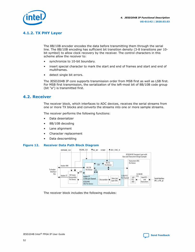
4.1.2. TX PHY Layer
The 8B/10B encoder encodes the data before transmitting them through the serialline. The 8B/10B encoding has sufficient bit transition density (3-8 transitions per 10-bit symbol) to allow clock recovery by the receiver. The control characters in thisscheme allow the receiver to:
• synchronize to 10-bit boundary.
• insert special character to mark the start and end of frames and start and end ofmultiframes.
• detect single bit errors.
The JESD204B IP core supports transmission order from MSB first as well as LSB first.For MSB first transmission, the serialization of the left-most bit of 8B/10B code group(bit "a") is transmitted first.
4.2. Receiver
The receiver block, which interfaces to ADC devices, receives the serial streams fromone or more TX blocks and converts the streams into one or more sample streams.
The receiver performs the following functions:
• Data deserializer
• 8B/10B decoding
• Lane alignment
• Character replacement
• Data descrambling
Figure 12. Receiver Data Path Block Diagram
Transceiver (RX)Per Device
RX FrameDeassemblyPer Device
RX CSRPer Device
RX CTLPer Device
Descrambler Data LinkLayer (RX)
SoftPCS(RX)
Hard PCSand
TransceiverJESD204B(RX) Per Device
CSR
CSR
CSR
32 Bit PCSPer Channel
32/40/80PCS
DEV_SYNC_NSYSREFRX_INTRXLINK_CLKRXFRAME_CLK
Avalon-MM
Avalon-ST
To AvalonInterface
Bus
JESD204 RX Transport Layer withBase and Transceiver Design Example
Avalon-ST32 Bits per Channel Serial Interface
(RX_n, RX_p)
The receiver block includes the following modules:
4. JESD204B IP Functional Description
UG-01142 | 2020.03.03
JESD204B Intel® FPGA IP User Guide Send Feedback
52
• RX CSR—manages the configuration and status registers.
• RX_CTL—manages the SYNC_N signal, state machine that controls the data linklayer states, LMFC, and also the buffer release, which is crucial for deterministiclatency throughout the link.
• RX Scrambler and Data Link Layer—takes in 32 bits of data that decodes the ILAS,performs descrambling, character replacement as per the JESD204B specification,and error detection (code group error, frame and lane realignment error).
4.2.1. RX Data Link Layer
The JESD204B IP core RX data link layer buffers incoming user data on all lanes untilthe RX elastic buffers can be released. Special character substitution are done in theTX link so that the RX link can execute frame and lane alignment monitoring based onthe JESD204B specification.
4.2.1.1. RX CGS
The CGS phase is the link up phase that monitors the detection of /K28.5/ character.
The CGS phase is achieved through the following process:
• Once the word boundary is aligned, the RX PHY layer detects the /K28.5/ 20-bitboundary and indicate that the character is valid.
• The receiver deasserts SYNC_N on the next frame boundary (for Subclass 0) or onthe next LMFC boundary (for Subclass 1 and 2) after the reception of foursuccessive /K/ characters.
• After correct reception of another four 8B/10B characters, the receiver assumesfull code group synchronization. Error detected in this state machine is the codegroup error. Code group error always trigger link reinitialization through theassertion of SYNC_N signal and this cannot be disabled through the CSR. The CSstate machine is defined as CS_INIT, CS_CHECK, and CS_DATA.
• The minimum duration for a synchronization request on the SYNC_N is five framesplus nine octets.
4.2.1.2. Frame Synchronization
After CGS phase, the receiver assumes that the first non-/K28.5/ character marks thestart of frame and multiframe. If the transmitter emits an initial lane alignmentsequence, the first non-/K28.5/ character is /K28.0/. Similar to the JESD204B TX IPcore, the csr_lane_sync_en is set to 1 by default, thus the RX core detects the /K/character to /R/ character transition. If the csr_lane_sync_en is set to 0, the RXcore detects the /K/ character to the first data transition. An ILAS error andunexpected /K/ character is flagged if either one of these conditions are violated.
When csr_lane_sync_en is set to 0, you have to disable data checking for the first16 octets of data as the character replacement block takes 16 octets to recover theend-of-frame pointer for character replacement. When csr_lane_sync_en is set to 1(default JESD204B setting), the number of octets to be discarded depends on thescrambler or descrambler block.
The receiver assumes that a new frame starts in every F octets. The octet counter isused for frame alignment and lane alignment.
4. JESD204B IP Functional Description
UG-01142 | 2020.03.03
Send Feedback JESD204B Intel® FPGA IP User Guide
53

Related Information
Scrambler/Descrambler on page 59
4.2.1.3. Frame Alignment
The frame alignment is monitored through the alignment character /F/. Thetransmitter inserts this character at the end of frame. The /A/ character indicates theend of multiframe. The character replacement algorithm depends on whetherscrambling is enabled or disabled, regardless of the csr_lane_sync_en registersetting.
The alignment detection process:
• If two successive valid alignment characters are detected in the same positionother than the assumed end of frame—without receiving a valid or invalidalignment character at the expected position between two alignment characters—the receiver realigns its frame to the new position of the received alignmentcharacters.
• If lane realignment can result in frame alignment error, the receiver issues anerror.
In the JESD204B RX IP core, the same flexible buffer is used for frame and lanealignment. Lane realignment gives a correct frame alignment because lane alignmentcharacter doubles as a frame alignment character. A frame realignment can cause anincorrect lane alignment or link latency. The course of action is for the RX to requestfor reinitialization through SYNC_N. (22)
4.2.1.4. Lane Alignment
After the frame synchronization phase has entered FS_DATA, the lane alignment ismonitored via /A/ character (/K28.3/) at the end of multiframe. The first /A/ detectionin the ILAS phase is important for the RX core to determine the minimum RX bufferrelease for inter-lane alignment. There are two types of error that is detected in lanealignment phase:
• Arrival of /A/ character from multiple lanes exceed one multiframe.
• Misalignment detected during user data phase.
The realignment rules for lane alignment are similar to frame alignment:
• If two successive and valid /A/ characters are detected at the same position otherthan the assumed end of multiframe—without receiving a valid/invalid /A/character at the expected position between two /A/ characters—the receiver alignsthe lane to the position of the newly received /A/ characters.
• If a recent frame alignment causes the loss of lane alignment, the receiverrealigns the lane frame—which is already at the position of the first received /A/character—at the unexpected position.
(22) Dynamic frame realignment and correction is not supported.
4. JESD204B IP Functional Description
UG-01142 | 2020.03.03
JESD204B Intel® FPGA IP User Guide Send Feedback
54

4.2.1.5. ILAS Data
The JESD204B RX IP core captures 14 octets of link configuration data that aretransmitted on the 2nd multiframe of the ILAS phase. The receiver waits for thereception of /Q/ character that marks the start of link configuration data and thenlatch it into ILAS octets, which are per lane basis. You can read the 14 octets capturedin the link configuration data through the CSR. You need to first set thecsr_ilas_data_sel register to select which link configuration data lane it is tryingto read from. Then, proceed to read from the csr_ilas_octet register.
4.2.1.6. Initial Lane Synchronization
The receivers in Subclass 1 and Subclass 2 modes store data in a memory buffer(Subclass 0 mode does not store data in the buffer but immediately releases them onthe frame boundary as soon as the latest lane arrives.). The RX IP core detects thestart of multiframe of user data per lane and then wait for the latest lane data toarrive. The latest data is reported as RBD count (csr_rbd_count) value which youcan read from the status register. This is the earliest release opportunity of the datafrom the deskew FIFO (referred to as RBD offset).
The JESD204B RX IP core supports RBD release at 0 offset and also providesprogrammable offset through RBD count. By default, the RBD release can beprogrammed through the csr_rbd_offset to release at the LMFC boundary. If youwant to implement an early release mechanism, program it in the csr_rbd_offsetregister. The csr_rbd_offset and csr_rbd_count is a counter based on the linkclock boundary (not frame clock boundary). Therefore, the RBD release opportunity isat every four octets.
4. JESD204B IP Functional Description
UG-01142 | 2020.03.03
Send Feedback JESD204B Intel® FPGA IP User Guide
55

Figure 13. Subclass 1 Deterministic Latency and Support for Programmable ReleaseOpportunity
K K K K K K K K K K K K K K K K K K K K K K K K K KR D D D D A R Q C C D D D AL Transmit Lanes
SYSREF
SYNC_N
LMFC
Deterministic Delay from SYSREF Sampled High to LMFC Zero-Crossing
TX ILA Begins on First LMFC Zero-Crossing after SYNC_N Is Deasserted
Multi-Frame
TXDevice
K K K K K K K K K K K K K R D D D D A R Q C C D D D A R D DEarliest Arrival Lane
SYSREF
SYNC_N
LMFC
Deterministic Delay fromSYSREF Sampled Highto LMFC Zero-Crossing
RX Elastic Buffers Released
RXDevice
K K
K K K K K K K K K K K K K R D D D D A R Q C C D D D A R D DK K
K K K K K K K K K K K K K R D D D D A R Q C C D D D A R D DK K
K K K K K K K K K K K KK K K K
K K K K K K K KK K K K
K KK K K K K K K K K K KK KK K K
Latest Arrival Lane
Aligned Output on All Lanes
RX Elastic BufferRelease Opportunity
RBD FrameCycles
SYNC_N Deasserted Directly after LMFC Zero Crossing
RBD FrameCycles
RBD FrameCycles
RBD FrameCycles
2 Character Elastic Buffer Delay for Latest Arrival6 Character Elastic Buffer Delay for Earliest Arrival
Deterministic Delayfrom TX ILA Output
to RX ILA Output
4.2.2. RX PHY Layer
The word aligner block identifies the MSB and LSB boundaries of the 10-bit characterfrom the serial bit stream. Manual alignment is set because the /K/ character must bedetected in either LSB first or MSB first mode. When the programmed word alignmentpattern is detected in the current word boundary, the PCS indicates a valid pattern inthe rx_sync_status (mapped as pcs_valid to the IP core). The codesynchronization state is detected after the detection of the /K/ character boundary forall lanes.
In a normal operation, whenever synchronization is lost, the JESD204B RX IP corealways return back to the CS_INIT state where the word alignment is initiated. Fordebug purposes, you can bypass this alignment by setting thecsr_patternalign_en register to 0.
The 8B/10B decoder decode the data after receiving the data through the serial line.The JESD204B IP core supports transmission order from MSB first as well as LSB first.
The PHY layer can detect 8B/10B not-in-table (NIT) error and also running disparityerror.
4.3. Operation
4. JESD204B IP Functional Description
UG-01142 | 2020.03.03
JESD204B Intel® FPGA IP User Guide Send Feedback
56
4.3.1. Operating Modes
The JESD204B IP core supports Subclass 0, 1, and 2 operating modes.
4.3.1.1. Subclass 0 Operating Mode
The JESD204B IP core maintains a LMFC counter that counts from 0 to (F × K/4)–1and wraps around again. The LMFC counter starts counting at the deassertion ofSYNC_N signal from multiple DACs after synchronization. This is to align the LMFCcounter upon transmission and can only be done after all the converter devices havedeasserted its synchronization request signal.
4.3.1.2. Subclass 1 Operating Mode
The JESD204B IP core maintains a LMFC counter that counts from 0 to (F × K/4)–1and wraps around again. The LMFC counter resets within two link clock cycles afterconverter devices issue a common SYSREF frequency to all the transmitters andreceivers. The SYSREF frequency must be the same for converter devices that aregrouped and synchronized together.
Table 21. Example of SYSREF Frequency CalculationIn this example, you can choose to perform one of the following options:
• provide two SYSREF and device clock, where the ADC groups share both the device clock and SYSREF(18.75 MHz and 9.375 MHz)
• provide one SYSREF (running at 9.375 MHz) and device clock for all the ADC and DAC groups because theSYSREF period in the DAC is a multiplication of n integer.
Group Configuration SYSREF Frequency
ADC Group 1 (2 ADCs) • LMF = 222• K = 16• Data rate = 6 Gbps
(6 GHz / 40) / (2 x 16 / 4) = 18.75 MHz
ADC Group 2 (2 ADCs) • LMF = 811• K = 32• Data rate = 6 Gbps
(6 GHz / 40) / (1 x 32 / 4) = 18.75 MHz
DAC Group 3 (2 DACs) • LMF = 222• K = 16• Data rate = 3 Gbps
(3 GHz / 40) / (2 x 16 / 4) = 9.375 MHz
4.3.1.3. Subclass 2 Operating Mode
The JESD204B IP core maintains a LMFC counter that counts from 0 to (F × K/4)–1and wraps around again. The LMFC count starts upon reset and the logic devicealways acts as the timing master. To support Subclass 2 for multi-link device, youmust deassert the resets for all JESD204B IP core links synchronously at the sameclock edge. This deassertion ensures that the internal LMFC vaunter is aligner acrossmulti-link. The converters adjust their own internal LMFC to match the master'scounter. The alignment of LMFC within the system relies on the correct alignment ofSYNC_N signal deassertion at the LMFC boundary.
The alignment of LMFC to RX logic is handled within the TX converter. The RX logicreleases SYNC_N at the LMFC tick and the TX converter adjust its internal LMFC tomatch the RX LMFC.
4. JESD204B IP Functional Description
UG-01142 | 2020.03.03
Send Feedback JESD204B Intel® FPGA IP User Guide
57

For the alignment of LMFC to the TX logic, the JESD204B TX IP core samples SYNC_Nfrom the DAC receiver and reports the relative phase difference between the DAC andTX logic device LMFC in the TX CSR (dbg_phadj, dbg_adjdir, and dbg_adjcnt).Based on the reported value, you can calculate the adjustment required. Then, toinitiate the link reinitialization through the CSR, set the value in the TX CSR(csr_phadj, csr_adjdir, and csr_adjcnt). The values on the phase adjustmentare embedded in bytes 1 and 2 of the ILAS sequence that is sent to the DAC duringlink initialization. On the reception of the ILAS, the DAC adjusts its LMFC phase bystep count value and sends back an error report with the new LMFC phaseinformation. This process may be repeated until the LMFC at the DAC and the logicdevice are aligned.
Table 22. dbg_phadj, dbg_adjdir and dbg_adjcnt Values for Different SYNC_NDeassertions
Case SYNC_N Signal Deassertion dbg_phadjValue
dbg_adjdirValue
dbg_adjcnt Value
1 Happens at LMFC boundary(23) 0 — —
2 Happens at LMFC count value that isequals or less than half of FxK/4value
1 0 Number of link clock cycles from theLMFC boundary to the detection ofSYNC_N signal deassertion
3 Happens at LMFC count value that ismore than half of FxK/4 value
1 1 Number of link clock cycles fromdetection of the SYNC_N signaldeassertion to the next LMFCboundary
Figure 14. Timing Diagram Example for Case 1
LMFC Boundaries
txlink_clk
sync_n
csr_f[7:0]
csr_k[4:0]
dbg_adjcnt[7:0]
dbg_adjdir
dbg_phadj
00
09
01
SYNC_N signal deassertion happens at LMFC boundary
(23) No adjustment is required.
4. JESD204B IP Functional Description
UG-01142 | 2020.03.03
JESD204B Intel® FPGA IP User Guide Send Feedback
58

Figure 15. Timing Diagram Example for Case 2
txlink_clk
sync_n
csr_f[7:0]
csr_k[4:0]
dbg_adjcnt[7:0]
dbg_adjdir
dbg_phadj
00 04
01
0f
LMFC Boundaries
SYNC_N signal deassertion happens at LMFC count value that is equals or less than half of FxK/4 value
Figure 16. Timing Diagram Example for Case 3
txlink_clk
sync_n
csr_f[7:0]
csr_k[4:0]
dbg_adjcnt[7:0]
dbg_adjdir
dbg_phadj
00 03
01
0f
LMFC Boundaries
SYNC_N signal deassertion happens at LMFC count value that is more than half of FxK/4 value
4.3.2. Scrambler/Descrambler
Both the scrambler and descrambler are designed in a 32-bit parallel implementationand the scrambling/descrambling order starts from first octet with MSB first.
The JESD204B TX and RX IP core support scrambling by implementing a 32-bit parallelscrambler in each lane. The scrambler and descrambler are located in the JESD204BIP MAC interfacing to the Avalon-ST interface. You can enable or disable scramblingand this option applies to all lanes. Mixed mode operation, where scrambling isenabled for some lanes, is not permitted.
The scrambling polynomial:
1 + x14 + x15
The descrambler can self-synchronize in eight octets. In a typical application wherethe reset value of the scrambler seed is different from the converter device to FPGAlogic device, the correct user data is recovered in the receiver in two link clocks (dueto the 32-bit architecture). The PRBS pattern checker on the transport layer shouldalways disable checking of the first eight octets from the JESD204B RX IP core.
4. JESD204B IP Functional Description
UG-01142 | 2020.03.03
Send Feedback JESD204B Intel® FPGA IP User Guide
59
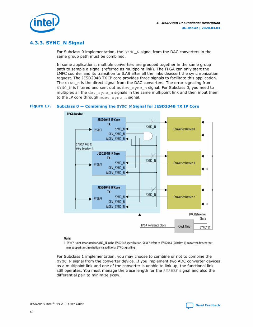
4.3.3. SYNC_N Signal
For Subclass 0 implementation, the SYNC_N signal from the DAC converters in thesame group path must be combined.
In some applications, multiple converters are grouped together in the same grouppath to sample a signal (referred as multipoint link). The FPGA can only start theLMFC counter and its transition to ILAS after all the links deassert the synchronizationrequest. The JESD204B TX IP core provides three signals to facilitate this application.The SYNC_N is the direct signal from the DAC converters. The error signaling fromSYNC_N is filtered and sent out as dev_sync_n signal. For Subclass 0, you need tomultiplex all the dev_sync_n signals in the same multipoint link and then input themto the IP core through mdev_sync_n signal.
Figure 17. Subclass 0 — Combining the SYNC_N Signal for JESD204B TX IP Core
SYSREF Tied to0 for Subclass 0
JESD204B IP CoreTX
SYSREF SYNC_NDEV_SYNC_N
MDEV_SYNC_N
SYSREF SYNC_NDEV_SYNC_N
MDEV_SYNC_N
SYSREF SYNC_NDEV_SYNC_N
MDEV_SYNC_N
FPGA Device
Converter Device 0
L
Converter Device 1
L
Converter Device 2
L
SYNC_N
SYNC_N
SYNC_N
Clock ChipFPGA Reference Clock SYNC* (1)
DAC ReferenceClock
Note:1. SYNC* is not associated to SYNC_N in the JESD204B specification. SYNC* refers to JESD204A (Subclass 0) converter devices that may support synchronization via additional SYNC signalling.
JESD204B IP CoreTX
JESD204B IP CoreTX
For Subclass 1 implementation, you may choose to combine or not to combine theSYNC_N signal from the converter device. If you implement two ADC converter devicesas a multipoint link and one of the converter is unable to link up, the functional linkstill operates. You must manage the trace length for the SYSREF signal and also thedifferential pair to minimize skew.
4. JESD204B IP Functional Description
UG-01142 | 2020.03.03
JESD204B Intel® FPGA IP User Guide Send Feedback
60

The SYNC_N is the direct signal from the DAC converters. The error signaling fromSYNC_N is filtered and sent out as dev_sync_n output signal. The dev_sync_nsignal from the JESD204B TX IP core must loopback into the mdev_sync_n signal ofthe same instance without combining the SYNC_N signal.
You must set the same RBD offset value (csr_rbd_offset) to all the JESD204B RXIP cores within the same multipoint link for the RBD release (the latest lane arrival foreach of the links). The JESD204B RX IP core deskews and outputs the data when theRBD offset value is met. The total latency is consistent in the system and is also thesame across multiple resets. Setting a different RBD offset to each link or setting anearly release does not guarantee deterministic latency and data alignment.
Figure 18. Subclass 1 — Combining the SYNC_N Signal for JESD204B TX IP Core
SYSREF (Subclass 1)
SYSREF
SYNC_NDEV_SYNC_N
MDEV_SYNC_N
SYSREF
SYNC_NDEV_SYNC_N
MDEV_SYNC_N
SYSREF
SYNC_NDEV_SYNC_N
MDEV_SYNC_N
FPGA Device
Converter Device 0
L
Converter Device 1
L
Converter Device 2
L
SYNC_N
SYNC_N
SYNC_N
Clock Chipand SYSREF
FPGA Reference Clock
SYSREF
DAC ReferenceClock
SYSREF
JESD204B IP CoreTX
JESD204B IP CoreTX
JESD204B IP CoreTX
Related Information
Programmable RBD Offset on page 150
4.3.4. Link Reinitialization
The JESD204B TX and RX IP core support link reinitialization.
4. JESD204B IP Functional Description
UG-01142 | 2020.03.03
Send Feedback JESD204B Intel® FPGA IP User Guide
61

There are two modes of entry for link reinitialization:
• Hardware initiated link reinitialization:
— For TX, the reception of SYNC_N for more than five frames and nine octetstriggers link reinitialization.
— For RX, the loss of code group synchronization, frame alignment and lanealignment errors cause the IP core to assert SYNC_N and request for linkreinitialization.
• Software initiated link reinitialization—both the TX and RX IP core allow softwareto request for link reinitialization.
— For TX, the IP core transmits /K/ character and wait for the receiver to assertSYNC_N to indicate that it has entered CS_INIT state.
— For RX, the IP core asserts SYNC_N to request for link reinitialization.
Hardware initiated link reinitialization can be globally disabled through thecsr_link_reinit_disable register for debug purposes.
Hardware initiated link reinitialization can be issued as interrupt depending on theerror type and interrupt error enable. If lane misalignment has been detected as aresult of a phase change in local timing reference, the software can rely on thisinterrupt trigger to initiates a LMFC realignment. The realignment process occurs byfirst resampling SYSREF and then issuing a link reinitialization request.
4.3.5. Link Startup Sequence
Set the run-time LMF configuration when the txlink_rst_n or rxlink_rst_nsignals are asserted. Upon txlink_rst_n or rxlink_rst_n deassertion, theJESD204B IP core begins operation. The following sections describe the detailedoperation for each subclass mode.
TX (Subclass 0)
Upon reset deassertion, the JESD204B TX IP core is in CGS phase. SYNC_Ndeassertion from the converter device enables the JESD204B TX IP core to exit CGSphase and enter ILAS phase (if csr_lane_sync_en = 1) or User Data phase (ifcsr_lane_sync_en = 0).
TX (Subclass 1)
Upon reset deassertion, the JESD204B TX IP core is in CGS phase. SYNC_Ndeassertion from the converter device enables the JESD204B TX IP core to exit CGSphase. The IP core ensures that at least one SYSREF rising edge is sampled beforeexiting CGS phase and entering ILAS phase. This is to prevent a race condition wherethe SYNC_N is deasserted before SYSREF is sampled. SYSREF sampling is crucial toensure deterministic latency in the JESD204B Subclass 1 system.
TX (Subclass 2)
Similar to Subclass 1 mode, the JESD204B TX IP core is in CGS phase upon resetdeassertion. The LMFC alignment between the converter and IP core starts afterSYNC_N deassertion. The JESD204B TX IP core detects the deassertion of SYNC_N andcompares the timing to its own LMFC. The required adjustment in the link clockdomain is updated in the register map. You need to update the final phase adjustment
4. JESD204B IP Functional Description
UG-01142 | 2020.03.03
JESD204B Intel® FPGA IP User Guide Send Feedback
62

value in the registers for it to transfer the value to the converter during the ILASphase. The DAC adjusts the LMFC phase and acknowledge the phase change with anerror report. This error report contains the new DAC LMFC phase information, whichallows the loop to iterate until the phase between them is aligned.
RX (Subclass 0)
The JESD204B RX IP core drives and holds SYNC_N (dev_sync_n signal) low when itis in reset. Upon reset deassertion, the JESD204B RX IP core checks if there issufficient /K/ character to move its state machine out of synchronization request.Once sufficient /K/ character is detected, the IP core deasserts SYNC_N.
RX (Subclass 1)
The JESD204B RX IP core drives and holds the SYNC_N (dev_sync_n signal) lowwhen it is in reset. Upon reset deassertion, the JESD204B RX IP core checks if there issufficient /K/ character to move its state machine out of synchronization request. TheIP core also ensures that at least one SYSREF rising edge is sampled beforedeasserting SYNC_N. This is to prevent a race condition where the SYNC_N isdeasserted based on internal free-running LMFC count instead of the updated LMFCcount after SYSREF is sampled.
RX (Subclass 2)
The JESD204B RX IP core behaves the same as in Subclass 1 mode. In this mode, thelogic device is always the master timing reference. Upon SYNC_N deassertion, the ADCadjusts the LMFC timing to match the IP core.
4.3.6. Error Reporting Through SYNC_N Signal
The JESD204B TX IP core can detect error reporting through SYNC_N when SYNC_N isasserted for two frame clock periods (if F >= 2) or four frame clock periods (if F = 1).When the downstream device reports an error through SYNC_N, the TX IP core issuesan interrupt. The TX IP core samples the SYNC_N pulse width using the link clock.
For a special case of F = 1, two frame clock periods are less than one link clock.Therefore, the error signaling from the receiver may be lost. You must program theconverter device to extend the SYNC_N pulse to four frame clocks when F = 1.
The JESD204B RX IP core does not report an error through SYNC_N signaling. Instead,the RX IP core issues an interrupt when any error is detected.
You can check the csr_tx_err, csr_rx_err0, and csr_rx_err1 register status todetermine the error types.
4.4. Clocking Scheme
This section describes the clocking scheme for the JESD204B IP core and transceiver.
4. JESD204B IP Functional Description
UG-01142 | 2020.03.03
Send Feedback JESD204B Intel® FPGA IP User Guide
63

Table 23. JESD204B IP Core Clocks
Clock Signal Formula Description
TX/RX Device Clock:pll_ref_clk
PLL selection during IP coregeneration
The PLL reference clock used by the TX Transceiver PLL orRX CDR.This is also the recommended reference clock to the PLLIntel FPGA IP core (for Arria V, Cyclone V, or Stratix Vdevices) or IOPLL Intel FPGA IP core (for Intel Arria 10,Intel Cyclone 10 GX, and Intel Stratix 10 devices).
TX/RX Link Clock:txlink_clk
rxlink_clk
Data rate/40 The timing reference for the JESD204B IP core.The linkclock runs at data rate/40 because the IP core operates in a32-bit data bus architecture after 8B/10B encoding.For Subclass 1, to avoid half link clock latency variation, youmust supply the device clock at the same frequency as thelink clock.The JESD204B transport layer in the design examplerequires both the link clock and frame clock to besynchronous.
TX/RX Frame Clock (indesign example):txframe_clk
rxframe_clk
Data rate/(10 × F) The frame clock as per the JESD204B specification. Thisclock is applicable to the JESD204B transport layer andother upstream devices that run in frame clock such as thePRBS generator/checker or any data processing blocks thatrun at the same rate as the frame clock.The JESD204B transport layer in the design example alsosupports running the frame clock in half rate or quarter rateby using the FRAMECLK_DIV parameter. The JESD204Btransport layer requires both the link clock and frame clockto be synchronous. For more information, refer to the F1/F2_FRAMECLK_DIV parameter description and itsrelationship to the frame clock in the respective JESD204BIntel FPGA IP design example user guides.
TX/RX Transceiver SerialClock and Parallel Clock
Internally derived from thedata rate during IP coregeneration
The serial clock is the bit clock to stream out serializeddata. The transceiver PLL supplies this clock and is internalto the transceiver.The parallel clock is for the transmitter PMA and PCS withinthe PHY. This clock is internal to the transceiver and is notexposed in the JESD204B IP core.For Arria V, Cyclone V, and Stratix V devices, these clocksare internally generated as the transceiver PLL isencapsulated within the JESD204B IP core's PHY.For Intel Arria 10, Intel Cyclone 10 GX, and Intel Stratix 10L-tile and H-tile devices, you need to generate thetransceiver PLL based on the data rate and connect theserial and parallel clock. You are recommended to selectmedium bandwidth for the transceiver PLL setting. Theseclocks are referred to as *serial_clk and*bonding_clock in Intel Arria 10, Intel Cyclone 10 GX,and Intel Stratix 10 L-tile and H-tile devices. Refer to therespective Transceiver PHY IP Core User Guides for moreinformation.
TX/RX PHY Clock:txphy_clk
rxphy_clk
Data rate/40 (for all devicesexcept Arria V GT/ST in PMADirect mode)Data rate/80 (forArria V GT/ST devices inPMA Direct mode)
The PHY clock generated from the transceiver parallel clockfor the TX path or the recovered clock generated from theCDR for the RX path.There is limited use for this clock. Avoid using this clockwhen PMA Direct mode is selected. Use this clock only if theJESD204B configuration is F=4 and the core is operating atSubclass 0 mode. This clock can be used as input for boththe txlink_clk and txframe_clk, or rxlink_clk andrxframe_clk.When you set the PCS option to enable Hard PCS or SoftPCS mode, the txphy_clk connects to the transceivertx_std_clkout signal and the rxphy_clk connects to
continued...
4. JESD204B IP Functional Description
UG-01142 | 2020.03.03
JESD204B Intel® FPGA IP User Guide Send Feedback
64

Clock Signal Formula Description
the rx_std_clkout signal. These are the clock lines at thePCS and FPGA fabric interface. When you enable PMA Directmode (for Arria V GT/ST only), the txphy_clk connects tothe transceiver tx_pma_clkout signal and the rxphy_clkconnects to the rx_pma_clkout signal. These are the clocklines at the PMA and PCS interface.
TX/RX AVS Clock:jesd204_tx_avs_clk
jesd204_rx_avs_clk
75–125 MHz The configuration clock for the JESD204B IP core CSRthrough the Avalon-MM interface.
Transceiver ManagementClock:reconfig_clk
100 MHz–125 MHz (IntelArria 10)100 MHz–125 MHz (IntelCyclone 10 GX)100 MHz–150 MHz (IntelStratix 10)
The configuration clock for the transceiver CSR through theAvalon-MM interface. This clock is exported only when thetransceiver dynamic reconfiguration option is enabled.This clock is only applicable for Intel Arria 10, Intel Cyclone10 GX, and Intel Stratix 10 devices.
Related Information
• Design Examples for JESD204B IP Core User GuideProvides information about design examples for Arria V, Cyclone V, Stratix V,and Intel Arria 10 devices using Intel Quartus Prime Standard Edition software.
• JESD204B Intel Arria 10 FPGA IP Design Example User Guide
• JESD204B Intel Stratix 10 FPGA IP Design Example User Guide
• JESD204B Intel Cyclone 10 GX FPGA IP Design Example User Guide
• JESD204B Intel Agilex FPGA IP Design Example User Guide
4.4.1. Device Clock
In a converter device, the sampling clock is typically the device clock.
For the JESD204B IP in an FPGA logic device, you need one or two reference clocks asshown in Figure 19 on page 66 and Figure 20 on page 67. In the single referenceclock design, the device clock is used as the transceiver PLL reference clock and alsothe core PLL reference clock. In the dual reference clock design, the device clock isused as the core PLL reference clock and the other reference clock is used as thetransceiver PLL reference clock. The available frequency depends on the PLL type,bonding option, number of lanes, and device family. During IP core generation, theIntel Quartus Prime software recommends the available reference frequency for thetransceiver PLL and core PLL based on user selection.
Note: Due to the clock network architecture in the FPGA, Intel recommends that you use thedevice clock to generate the link clock and use the link clock as the timing reference.You need to use the PLL Intel FPGA IP core (in Arria V, Cyclone V, and Stratix Vdevices) or IOPLL Intel FPGA IP core (in Intel Arria 10, Intel Cyclone 10 GX, and IntelStratix 10 devices) to generate the link clock and frame clock. The link clock is used inthe JESD204B IP (MAC) and the transport layer. You are recommended to supply thereference clock source through a dedicated reference clock pin.
Based on the JESD204B specification for Subclass 1, the device clock is the timingreference and is source synchronous with SYSREF. To achieve deterministic latency,match the board trace length of the SYSREF signal with the device clock. Maintain aconstant phase relationship between the device clock and SYSREF signal pairs going tothe FPGA and converter devices. Ideally, the SYSREF pulses from the clock generator
4. JESD204B IP Functional Description
UG-01142 | 2020.03.03
Send Feedback JESD204B Intel® FPGA IP User Guide
65

should arrive at the FPGA and converter devices at the same time. To avoid half linkclock latency variation, you must supply the device clock at the same frequency as thelink clock.
The JESD204B protocol does not support rate matching. Therefore, you must ensurethat the TX or RX device clock (pll_ref_clk) and the PLL reference clock thatgenerates link clock (txlink_clk or rxlink_clk) and frame clock (txframe_clkor rxframe_clk) have 0 ppm variation. Both PLL reference clocks should come fromthe same clock chip.
Figure 19. JESD204B Subsystem with Shared Transceiver Reference Clock and CoreClock
Note: This diagram is not applicable for Intel Agilex and Intel Stratix 10 E-tile devices.
Clock Generator
Converter Device
Converter Device
mgmt_clock
ClockSYSREF
Trace Matching
MAC PHY
TransceiverPLL (2)
JESD204B IP
Core PLLFPGA Device(Normal Mode) (3)
JESD204BTransport
LayerUser Logic
Avalon-STAvalon-ST
Link Clock
Frame Clock avs_clock
Trace Matching (1)
SYSREF
FPGA DeviceClock
Notes:1. The device clock to the Intel core PLL and SYSREF must be trace matched. The device clock to the converter device and SYSREF must be trace matched. The phase offset between the SYSREF to the FPGA and converter devices should be minimal.2. For Intel Arria 10, Intel Cyclone 10 GX, and Intel Stratix 10 L-tile and H-tile devices, the transceiver PLL is outside of the JESD204B IP. For Arria V, Cyclone V, and Stratix V devices, the transceiver PLL is part of the JESD204B IP.3. The core PLL provides the link clock and frame clock. The link clock and frame clock must be synchronous. The AVS clock (e.g. mgmt_clk) can be asynchronous to the link and frame clock.
(1)
4. JESD204B IP Functional Description
UG-01142 | 2020.03.03
JESD204B Intel® FPGA IP User Guide Send Feedback
66

Figure 20. JESD204B Subsystem with Separate Transceiver Reference Clock and CoreClock
Converter Device
Converter DeviceClock
SYSREF
Trace Matching
MAC PHY
TransceiverPLL (2)
JESD204B IP Core
Core PLLFPGA Device
(Normal Mode) (3)
JESD204BTransport
LayerUser Logic
Avalon-STAvalon-ST
Link Clock
Frame Clock avs_clock
Trace Matching
SYSREF FPGA Device Clock
FPGA TransceiverReference Clock
Notes:1. The device clock to the Intel core PLL and SYSREF must be trace matched. The device clock to the converter device and SYSREF must be trace matched. The phase offset between the SYSREF to the FPGA and converter devices should be minimal.2. For Intel Arria 10, Intel Cyclone 10 GX, and Intel Stratix 10 L-tile and H-tile devices, the transceiver PLL is outside of the JESD204B IP core. For Arria V, Cyclone V, Stratix V, and Intel Stratix 10 E-tile devices, the transceiver PLL is part of the JESD204B IP core.3. The core PLL provides the link clock and frame clock. The link clock and frame clock must be synchronous. The AVS clock (e.g. mgmt_clk) can be asynchronous to the link and frame clock.4. You must use a dedicated reference clock input for the core PLL to compensate the FPGA clock network latency. This ensures that SYSREF is captured without any cycle variation.
Clock Generator
(1)
(1)
(4)
mgmt_clock
Related Information
Clock Correlation on page 69
4.4.2. Link Clock
The device clock is the timing reference for the JESD204B system.
Due to the clock network architecture in the FPGA, JESD204B IP core does not use thedevice clock to clock the SYSREF signal because the GCLK or RCLK is not fullycompensated. You are recommended to use the PLL Intel FPGA IP core (in Arria V,Cyclone V, and Stratix V devices) or IOPLL Intel FPGA IP core (in Intel Arria 10, IntelCyclone 10 GX, and Intel Stratix 10 devices) to generate both the link clock and frameclock. The PLL Intel FPGA IP core must operate in normal mode or sourcesynchronous mode and uses a dedicated reference clock pin as the input referenceclock source to achieve the following state:
• the GCLK and RCLK clock network latency is fully compensated.
• the link clock and frame clock at the registers are phase-aligned to the input ofthe clock pin.
To provide consistency across the design regardless of frame clock and sampling clock,the link clock is used as a timing reference.
The PLL Intel FPGA IP core should provide both the frame clock and link clock from thesame PLL as these two clocks are treated as synchronous in the design.
For Subclass 0 mode, the device clock is not required to sample the SYSREF signaledge. The link clock does not need to be phase compensated to capture SYSREF.Therefore, you can generate both the link clock and frame clock using direct mode in
4. JESD204B IP Functional Description
UG-01142 | 2020.03.03
Send Feedback JESD204B Intel® FPGA IP User Guide
67

the PLL Intel FPGA IP core. If F = 4, where link clock is the same as the frame clock,you can use the parallel clock output from the transceiver (txphy_clk or rxphy_clksignal) except when the PCS option is in PMA Direct mode.
Related Information
Clock Correlation on page 69
4.4.3. Local MultiFrame Clock
The Local MultiFrame Clock (LMFC) is a counter generated from the link clock anddepends on the F and K parameter.
The K parameter must be set between 1 to 32 and meet the requirement of at least aminimum of 17 octets and a maximum of 1024 octets in a single multiframe. In a 32-bit architecture, the K × F must also be in the order of four.
In a Subclass 1 deterministic latency system, the SYSREF frequency is distributed tothe devices to align them in the system. The SYSREF resets the internal LMFC clockedge when the sampled SYSREF signal's rising edge transition from 0 to 1. Due tosource synchronous signaling of SYSREF with respect to the device clock sampling(provided from the clock chip), the JESD204B IP core does not directly use the deviceclock to sample SYSREF but instead uses the link clock to sample SYSREF. Therefore,the Intel FPGA PLL IP core that provides the link clock must to be in normal mode tophase-compensate the link clock to the device clock.
Based on hardware testing, to get a fixed latency, at least 32 octets are recommendedin an LMFC period so that there is a margin to tune the RBD release opportunity tocompensate any lane-to-lane deskew across multiple resets. If F = 1, then K = 32 isoptimal as it provides enough margin for system latency variation. If F = 2, then K =16 and above (18/20/22/24/26/28/30/32) is sufficient to compensate lane-to-lanedeskew.
The JESD204B IP core implements the local multiframe clock as a counter thatincrements in link clock counts. The local multiframe clock counter is equal to (F ×K/4) in link clock as units. The rising edge of SYSREF resets the local multiframe clockcounter to 0. There are two CSR bits that controls SYSREF sampling.
• csr_sysref_singledet—resets the local multiframe clock counter once andautomatically cleared after SYSREF is sampled. This register also prevents CGSexit to bypass SYSREF sampling.
• csr_sysref_alwayson—resets the local multiframe clock counter at every risingedge of SYSREF that it detects. This register also enables the SYSREF periodchecker. If the provided SYSREF period violates the F and K parameter, aninterrupt is triggered. However, this register does not prevent CGS-SYSREF racecondition.
The following conditions occur if both CSR bits are set:
• resets the local multiframe clock counter at every rising edge of SYSREF.
• prevents CGS-SYSREF race condition.
• checks SYSREF period.
Related Information
Clock Correlation on page 69
4. JESD204B IP Functional Description
UG-01142 | 2020.03.03
JESD204B Intel® FPGA IP User Guide Send Feedback
68
4.4.4. Clock Correlation
This section describes the clock correlation between the device clock, link clock, frameclock, and local multiframe clock.
Example 1
Targeted Device with LMF=222, K=16 and Data rate = 6.5 Gbps
Device Clock Selected = 325 MHz (obtained during IP core generation)
Link Clock = 6.5 GHz/40 = 162.5 MHz
Frame Clock = 6.5 GHz/(10x2) = 325 MHz
Local Multiframe Clock = 325 MHz / 16 = 20.3125 MHz
SYSREF Frequency = Local Multiframe Clock / n; (n = integer; 1, 2, …)
Local Multiframe Clock Counter = (F × K/4) = (2×16/4) = 8 link clocks (24)
Example 2
Targeted Device with LMF=244, K=16 and Data rate = 5.0 Gbps
Device Clock Selected = 125 MHz (obtained during IP core generation)
Link Clock = 5 GHz/40 = 125 MHz (25)
Frame Clock = 5 GHz /(10×4) = 125 MHz (25)
Local Multiframe Clock = 125 MHz / 16 = 7.8125 MHz
SYSREF Frequency = Local Multiframe Clock / n; (n = integer; 1, 2, …)
Local Multiframe Clock Counter = (F × K/4) = (4×16/4) = 16 link clocks (24)
Example 3
Targeted Device with LMF=421, K=32 and Data rate = 10.0 Gbps
Device Clock Selected = 250 MHz (obtained during IP core generation)
Link Clock = 10 GHz/40 = 250 MHz
Frame Clock = 10 GHz/(10×1) = 1 GHz (26)
(24) Eight link clocks mean that the local multiframe clock counts from values 0 to 7 and then loopsback to 0.
(25) The link clock and frame clock are running at the same frequency. You only need to generateone clock from the Intel FPGA PLL or Intel FPGA IO PLL IP core.
(26) In this example, the frame clock may not be able to run up to 1 GHz in the FPGA fabric. TheJESD204B transport layer in the design example supports running the data stream of half rate(1 GHz/2 = 500 MHz), at two times the data bus width or of quarter rate (1GHz/4 = 250 MHz),at four times the data bus width.
4. JESD204B IP Functional Description
UG-01142 | 2020.03.03
Send Feedback JESD204B Intel® FPGA IP User Guide
69

Local Multiframe Clock = 1 GHz / 32 = 31.25 MHz
SYSREF Frequency = Local Multiframe Clock / n; (n = integer; 1, 2, …)
Local Multiframe Clock Counter = (F × K/4) = (1×32/4) = 8 link clocks (24)
Example 4 (When F=3, for Intel Stratix 10 devices only)
Targeted Device with LMF=883, K=32 and Data rate = 12.0 Gbps
Device Clock Selected = 300 MHz (obtained during IP core generation)
Link Clock = 12 GHz/40 = 300 MHz
Frame Clock = 12 GHz/(10×3) = 400 MHz (27)
Local Multiframe Clock = 400 MHz / 32 = 12.5 MHz
SYSREF Frequency = Local Multiframe Clock / n; (n = integer; 1, 2, …)
Local Multiframe Clock Counter = (F × K/4) = (3×32/4) = 24 link clocks (24)
Related Information
• Device Clock on page 65
• Link Clock on page 67
• Local MultiFrame Clock on page 68
4.5. Reset Scheme
All resets in the JESD204B IP are synchronous reset signals and should be assertedand deasserted synchronously.
Note: Ensure that the resets are synchronized to the respective clocks for reset assertionand deassertion.
Table 24. JESD204B IP Resets
Reset Signal Associated Clock Description
txlink_rst_n
rxlink_rst_n
TX/RX Link Clock Active low reset. Intel recommends that you:• Assert the txlink_rst_n/rxlink_rst_n and
txframe_rst_n /rxframe_rst_n signals whenthe transceiver is in reset.
• Deassert the txlink_rst_n andtxframe_rst_n signals after the Intel FPGA PLLIP is locked and the tx_ready[] signal from theTransceiver Reset Controller is asserted.
• Deassert the rxlink_rst_n andrxframe_rst_n signals after the Transceiver CDRrx_islockedtodata[] signal and rx_ready[]signal from the Transceiver Reset Controller areasserted.
continued...
(27) The JESD204B transport layer in the design example runs the data stream at half rate (400MHz/2 = 200 MHz), two times the data bus width.
4. JESD204B IP Functional Description
UG-01142 | 2020.03.03
JESD204B Intel® FPGA IP User Guide Send Feedback
70

Reset Signal Associated Clock Description
The txlink_rst_n/rxlink_rst_n andtxframe_rst_n /rxframe_rst_n signals can bedeasserted at the same time. These resets can only bedeasserted after you configure the CSR registers.
txframe_rst_n
rxframe_rst_n
TX/RX Frame Clock Active low reset controlled by the clock and reset unit.If the TX/RX link clock and the TX/RX frame clock hasthe same frequency, both can share the same reset.
tx_analogreset[L-1:0]
rx_analogreset[L-1:0]
Transceiver Native PHYAnalog Reset
Active high reset controlled by the transceiver resetcontroller. This signal resets the TX/RX PMA.The link clock, frame clock, and AVS clock resetsignals (txlink_rst_n/rxlink_rst_n,txframe_rst_n/rxframe_rst_n andjesd204_tx_avs_rst_n/jesd204_rx_avs_rst_n)can only be deasserted after the transceiver comesout of reset. (28)
Note: This signal is not applicable for Intel Agilex andIntel Stratix 10 E-tile devices.
tx_analogreset_stat[L-1:0]
rx_analogreset_stat[L-1:0]
Transceiver Native PHYAnalog Reset
TX PMA analog reset status port connected to thetransceiver reset controller.(29)
Note: This signal is applicable only for Intel Stratix10 L-tile and H-tile devices.
tx_digitalreset[L-1:0]
rx_digitalreset[L-1:0]
Transceiver Native PHYDigital Reset
Active high reset controlled by the transceiver resetcontroller. This signal resets the TX/RX PCS.The link clock, frame clock, and AVS clock resetsignals (txlink_rst_n/rxlink_rst_n,txframe_rst_n/rxframe_rst_n andjesd204_tx_avs_rst_n/jesd204_rx_avs_rst_n)can only be deasserted after the transceiver comesout of reset. (28)
Note: This signal is not applicable for Intel Agilex andIntel Stratix 10 E-tile devices.
tx_digitalreset_stat[L-1:0]
rx_digitalreset_stat[L-1:0]
Transceiver Native PHYDigital Reset
TX PCS digital reset status port connected to thetransceiver reset controller.(29)
Note: This signal is applicable only for Intel Stratix10 L-tile and H-tile devices.
jesd204_tx_avs_rst_n
jesd204_rx_avs_rst_n
TX/RX AVS (CSR) Clock Active low reset controlled by the clock and reset unit.Typically, both signals can be deasserted after the corePLL and transceiver PLL are locked and out of reset. Ifyou want to dynamically modify the LMF at run-time,you can program the CSRs after AVS reset isdeasserted. This phase is referred to as theconfiguration phase.After the configuration phase is complete, then onlythe txlink_rst_n/rxlink_rst_n andtxframe_rst_n/rxframe_rst_n signals can bedeasserted.
Related Information
• V-Series Transceiver PHY User Guide
(28) Refer to the respective Transceiver PHY IP User Guides for the timing diagram of thetx_analogreset, rx_analogreset, tx_digitalreset, and rx_digitalreset signals.
(29) Refer to the Intel Stratix 10 L- and H-tile Transceiver PHY IP User Guide for the timingdiagram of the tx_analogreset_stat, rx_analogreset_stat,tx_digitalreset_stat, and rx_digitalreset_stat signals.
4. JESD204B IP Functional Description
UG-01142 | 2020.03.03
Send Feedback JESD204B Intel® FPGA IP User Guide
71
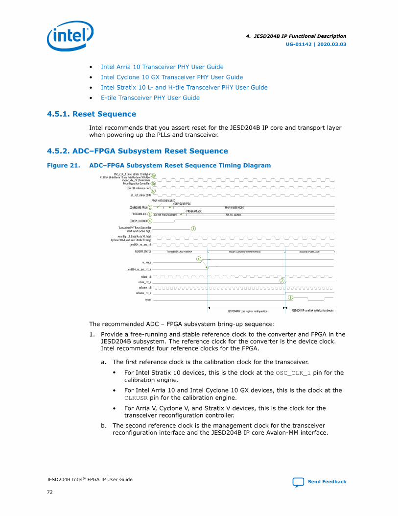
• Intel Arria 10 Transceiver PHY User Guide
• Intel Cyclone 10 GX Transceiver PHY User Guide
• Intel Stratix 10 L- and H-tile Transceiver PHY User Guide
• E-tile Transceiver PHY User Guide
4.5.1. Reset Sequence
Intel recommends that you assert reset for the JESD204B IP core and transport layerwhen powering up the PLLs and transceiver.
4.5.2. ADC–FPGA Subsystem Reset Sequence
Figure 21. ADC–FPGA Subsystem Reset Sequence Timing Diagram
pll_ref_clk (rx CDR)
Core PLL reference clock
CLKUSR (Intel Arria 10 and Intel Cyclone 10 GX) orOSC_CLK_1 (Intel Stratix 10 only) or
mgmt_clk_clk (Transceiver Reconfiguration Controller)
GENERIC STATES
CONFIGURE FPGA
PROGRAM ADC
CORE PLL LOCKED
TRANSCEIVER & PLL POWERUP JESD204B IP OPERATION
rxlink_clk
rxlink_rst_n
rxframe_clk
rxframe_rst_n
sysref
PROGRAM ADCFPGA IN USER MODE
CONFIGURE FPGAFPGA NOT CONFIGURED
ADC PLL LOCKEDADC NOT PROGRAMMED
JESD204B IP core register configuration JESD204B IP core link initialization begins
AVALON SLAVE CONFIGURATION PHASE
reconfig_clk (Intel Arria 10, Intel Cyclone 10 GX, and Intel Stratix 10 only)
Transceiver PHY Reset Controllerreset input (active high)
jesd204_rx_avs_clk
rx_ready
jesd204_rx_avs_rst_n
1a1a
1b1b
1c1c
22
33
44
55
66
77
88
The recommended ADC – FPGA subsystem bring-up sequence:
1. Provide a free-running and stable reference clock to the converter and FPGA in theJESD204B subsystem. The reference clock for the converter is the device clock.Intel recommends four reference clocks for the FPGA.
a. The first reference clock is the calibration clock for the transceiver.
• For Intel Stratix 10 devices, this is the clock at the OSC_CLK_1 pin for thecalibration engine.
• For Intel Arria 10 and Intel Cyclone 10 GX devices, this is the clock at theCLKUSR pin for the calibration engine.
• For Arria V, Cyclone V, and Stratix V devices, this is the clock for thetransceiver reconfiguration controller.
b. The second reference clock is the management clock for the transceiverreconfiguration interface and the JESD204B IP core Avalon-MM interface.
4. JESD204B IP Functional Description
UG-01142 | 2020.03.03
JESD204B Intel® FPGA IP User Guide Send Feedback
72

• If the dynamic reconfiguration option is enabled for Intel Arria 10, IntelCyclone 10 GX, and Intel Stratix 10 devices, this reference clock isconnected to the reconfig_clk input port of the JESD204B IP core.
c. The third reference clock is the transceiver reference clock.
• For Intel Stratix 10, you must provide the reference clock at thetransceiver dedicated reference clock input pin.
• For Intel Arria 10, Intel Cyclone 10 GX, Arria V, Cyclone V, and Stratix Vdevices, this clock is also used as the reference clock for the core PLL(IOPLL Intel FPGA IP core for Intel Arria 10 and Intel Cyclone 10 GXdevices; and PLL Intel FPGA IP core for Arria V, Cyclone V, and Stratix Vdevices) if you share the device clock and the transceiver reference clock(refer to Figure 19 on page 66).
d. The fourth reference clock is the core PLL reference clock (device clock).
• For Intel Stratix 10, you must provide the reference clock at the dedicatedreference clock input pin at the IO bank.
• For Intel Arria 10, Intel Cyclone 10 GX, Arria V, Cyclone V, and Stratix Vdevices, this is the reference clock for the core PLL (IOPLL Intel FPGA IPcore for Intel Arria 10 and Intel Cyclone 10 GX devices; and PLL IntelFPGA IP core for Arria V, Cyclone V, and Stratix V devices) if you do notshare the device clock and the transceiver reference clock (refer to Figure19 on page 66).
2. Configure the FPGA. Hold the RX transceiver channel in reset.
• For Intel Arria 10 and Intel Cyclone 10 GX devices, if the reference clock is notavailable for the transceiver CDR before the FPGA is configured, you need tohold the RX transceiver channels in reset and perform user calibration for theRX transceiver channels after the reference clock is stable. For moreinformation about user calibration for the transceiver channels, refer to theCalibration chapter in the Intel Arria 10 or Intel Cyclone 10 GX TransceiverPHY User Guides.
3. You can program the ADC through its SPI interface before or after configuring theFPGA. Ensure that the ADC PLL is locked before you proceed to the next step.
4. Ensure that the FPGA device clock core PLL is locked to the reference clock.
5. Deassert the FPGA RX transceiver channel reset. Do this by deasserting the resetinput pin of the Transceiver PHY Reset Controller.
6. Once the transceiver is out of reset (the rx_ready signal from the Intel FPGATransceiver PHY Reset Controller is asserted), deassert the Avalon-MM interfacereset for the IP core. At the configuration phase, the subsystem can program theJESD204B IP core if the default IP core register settings need to change.
7. Deassert both the link reset for the IP core and the frame reset for the transportlayer.
8. For subclass 1, if the continuous SYSREF pulses from the clock generator arepresent when the RX link reset is deasserted, the ADC-RX link initializes. If theSYSREF pulse is not present, trigger the clock generator to provide a SYSREFpulse to initialize the link. For subclass 0, the link initializes after the ADC isprogrammed and the RX link reset is deasserted.
Related Information
• V-Series Transceiver PHY User Guide
4. JESD204B IP Functional Description
UG-01142 | 2020.03.03
Send Feedback JESD204B Intel® FPGA IP User Guide
73

• Intel Arria 10 Transceiver PHY User Guide
• Intel Cyclone 10 GX Transceiver PHY User Guide
• Intel Stratix 10 L- and H-tile Transceiver PHY User Guide
• E-tile Transceiver PHY User Guide
4.5.3. FPGA–DAC Subsystem Reset Sequence
Figure 22. FPGA–DAC Subsystem Reset Sequence Timing Diagram
pll_ref_clk (TX PLL)
Core PLL reference clock
CLKUSR (Intel Arria 10 and Intel Cyclone 10 GX) ormgmt_clk_clk (Transceiver
Reconfiguration Controller)
GENERIC STATES
CONFIGURE FPGA
PROGRAM DAC
CORE PLL LOCKED
TRANSCEIVER & PLL POWERUP JESD204B IP OPERATION
pll_locked (from TX PLL)
txlink_clk
txlink_rst_n
txframe_clk
txframe_rst_n
tx_serial_data
sysref
PROGRAM DAC
/K/
FPGA IN USER MODECONFIGURE FPGA
FPGA NOT CONFIGURED
DAC PLL LOCKEDDAC NOT PROGRAMMED
JESD204B IP core register configuration JESD204B IP core link initialization begins
AVALON SLAVE CONFIGURATION PHASE
reconfig_clk (Intel Arria 10 and Cyclone 10 GX only)
Transceiver PHY Reset Controllerreset input (active high)
jesd204_tx_avs_clk
Transceiver PHY Reset Controller
tx_ready
jesd204_tx_avs_rst_n
1a1a
1b1b
1c1c
22
33
44
55
66
88
1010
77
99
OSC_CLK_1 (Intel Stratix 10 only) or
The recommended FPGA – DAC subsystem bring-up sequence:
1. Provide a free-running and stable reference clock to the converter and FPGA in theJESD204B subsystem. The reference clock for the converter is the device clock.Intel recommends four reference clocks for the FPGA.
a. The first reference clock is the calibration clock for the transceiver.
• For Intel Stratix 10 devices, this is the clock at the OSC_CLK_1 pin for thecalibration engine.
• For Intel Arria 10 and Intel Cyclone 10 GX devices, this is the clock at theCLKUSR pin for the calibration engine.
• For Stratix V, Arria V, and Cyclone V devices, this is the clock for thetransceiver reconfiguration controller.
b. The second reference clock is the management clock for the transceiverreconfiguration interface and the JESD204B IP core Avalon MM interface.
• If the dynamic reconfiguration option is enabled for Intel Arria 10, IntelCyclone 10 GX, and Intel Stratix 10 devices, this reference clock isconnected to the reconfig_clk input port of the JESD204B IP core.
c. The third reference clock is the transceiver reference clock.
4. JESD204B IP Functional Description
UG-01142 | 2020.03.03
JESD204B Intel® FPGA IP User Guide Send Feedback
74

• For Intel Stratix 10, you must provide the reference clock at thetransceiver dedicated reference clock input pin.
• For Intel Arria 10, Intel Cyclone 10 GX, Arria V, Cyclone V, and Stratix V,this clock is also used as the reference clock for the core PLL (IOPLL IntelFPGA IP core for Intel Arria 10 and Intel Cyclone 10 GX; and PLL IntelFPGA IP core for Arria V, Cyclone V, and Stratix V devices) if you share thedevice clock and the transceiver reference clock (refer to Figure 19 onpage 66).
d. The fourth reference clock is the core PLL reference clock (device clock).
• For Intel Stratix 10, you must provide the reference clock at the dedicatedreference clock input pin at the IO bank.
• For Intel Arria 10, Intel Cyclone 10 GX, Arria V, Cyclone V, and Stratix V,this is the reference clock for the core PLL (IOPLL Intel FPGA IP core forIntel Arria 10 and Intel Cyclone 10 GX devices; and PLL Intel FPGA IP corefor Arria V, Cyclone V, and Stratix V devices) if you do not share the deviceclock and the transceiver reference clock (refer to Figure 20 on page 67).
2. Configure the FPGA. Hold the TX transceiver PLL and channel in reset.
• For Intel Arria 10 and Intel Cyclone 10 GX devices, if the reference clock is notavailable for the transceiver PLL before the FPGA is configured, you need tohold the transceiver PLL and channels in reset and perform user calibration forthe transceiver PLL and TX channels after the reference clock is stable. Formore information about user calibration for the transceiver PLL and channels,refer to the Calibration chapter in the Intel Arria 10 or Intel Cyclone 10 GXTransceiver PHY User Guides.
3. Ensure that the FPGA device clock core PLL is locked to the reference clock.
4. Deassert the FPGA TX transceiver PLL and channel reset. Do this by deassertingthe reset input pin of the Transceiver PHY Reset Controller.
5. Ensure that the FPGA transceiver PLL is locked to the reference clock.
6. Once the TX transceiver PLL and channel are out of reset (the tx_ready signalfrom the Transceiver PHY Reset Controller is asserted), deassert the Avalon-MMinterface reset for the IP core. At the configuration phase, the subsystem canprogram the JESD204B IP core if the default IP core register settings need tochange.
7. Deassert both the link reset for the IP core and the frame reset for the transportlayer.
8. The TX IP core streams /K/ characters to the DAC after TX link reset is deasserted.
9. Program the DAC through its SPI interface.
10. For subclass 1, if the continuous SYSREF pulses from the clock generator arepresent when the TX link reset is deasserted, the TX-DAC link initializes. If theSYSREF pulse is not present, trigger the clock generator to provide a SYSREFpulse to initialize the link.
11. For subclass 0, the link initializes after the DAC is programmed and the TX linkreset is deasserted.
4. JESD204B IP Functional Description
UG-01142 | 2020.03.03
Send Feedback JESD204B Intel® FPGA IP User Guide
75

4.6. Signals
The JESD204B IP core signals are listed by interface:
• Transmitter
• Receiver
Note: You should terminate any unused signals.
4. JESD204B IP Functional Description
UG-01142 | 2020.03.03
JESD204B Intel® FPGA IP User Guide Send Feedback
76

4.6.1. Transmitter Signals
Figure 23. Transmitter Signal DiagramL denotes the number of lanes.
pll_ref_clkClock and Reset
JESD204B TX
Transceiver Interface
Avalon-ST Interface
Avalon-MM Interface
JESD204B Interface
CSR
txlink_clktxlink_rst_n_reset_n
txphy_clk[L-1:0]
tx_digitalreset[L-1:0]tx_analogreset[L-1:0]
pll_locked[L-1:0]
tx_cal_busy[L-1:0]
tx_digitalreset_stat[L-1:0]tx_analogreset_stat[L-1:0]
pll_powerdown[1]
tx_bonding_clocks[2]tx_serial_clk0[2]
tx_serial_data[L-1:0]
tx_serial_data_n[L-1:0]phy_tx_ready[L-1:0]phy_tx_pma_ready[L-1:0]phy_tx_rst_n[1:0]
reconfig_clk[3]
Note:1.2.3.
Refer to the Transmitter Signals table for actual signal width.Refer to the Transmitter Signals table for actual signal name.Refer to the Transmitter Signals table for actual signal width and name.
reconfig_reset[3]reconfig_avmm_address[3]
reconfig_avmm_writedata[3]reconfig_avmm_readdata[3]
reconfig_avmm_write[3]reconfig_avmm_read[3]
reconfig_avmm_waitrequest[3]
jesd204_tx_link_data[(L*32)-1:0]jesd204_tx_link_valid
jesd204_tx_link_readyjesd204_tx_frame_ready
jesd204_tx_avs_clkjesd204_tx_avs_rst_njesd204_tx_avs_chipselectjesd204_tx_avs_address[7:0]jesd204_tx_avs_writedata[31:0]
jesd204_tx_avs_readjesd204_tx_avs_write
jesd204_tx_avs_readdata[31:0]jesd204_tx_avs_waitrequest
sysrefsync_ndev_sync_n
mdev_sync_nsomf[3:0]
jesd204_tx_frame_errorcsr_l[4:0]csr_f[7:0]csr_k[4:0]csr_m[7:0]csr_cs[1:0]
csr_n[4:0]csr_np[4:0]
csr_s[4:0]
csr_hdcsr_cf[4:0]
csr_lane_powerdown[L-1:0]
Out-of-bandjesd204_tx_int
csr_tx_testpattern_a[31:0]Debug or Testing csr_tx_testmode[3:0]
csr_tx_testpattern_b[31:0]csr_tx_testpattern_c[31:0]csr_tx_testpattern_d[31:0]
jesd204_tx_dlb_data[(L*32)-1:0]jesd204_tx_dlb_kchar_data[(L*4)-1:0]
reconfig_to_xcvr[1]reconfig_from_xcvr[1]
Available inArria V, Cyclone Vand Stratix Vdevices only
Available inArria V, Cyclone Vand Stratix Vdevices only
Available in Intel Agilex andIntel Stratix 10 E-tile devices only
Available in Intel Arria 10, Intel Cyclone 10 GX, Intel Stratix 10, and Intel Agilex devices only
Available in Intel Stratix 10 L-tile and H-tile devices only
Available in Intel Arria 10, Intel Cyclone 10 GX, Intel Stratix 10,and Intel Agilex devices only
Not available in Intel Agilex andIntel Stratix 10 E-tile devices
pll_locked[L-1:0]Available in Intel Arria 10, Intel Cyclone 10 GX, and Intel Stratix 10 L-tile and H-tile devices only
4. JESD204B IP Functional Description
UG-01142 | 2020.03.03
Send Feedback JESD204B Intel® FPGA IP User Guide
77

Table 25. Transmitter Signals
Signal Width Direction Description
Clocks and Resets
pll_ref_clk 1 Input Transceiver reference clock signal.The reference clock selectiondepends on the FPGA device familyand data rate.This signal is only applicable forArria V, Cyclone V, and Stratix Vdevices.
txlink_clk 1 Input TX link clock signal. This clock isequal to the TX data rate dividedby 40.For Subclass 1, you cannot use theoutput of txphy_clk signal astxlink_clk signal . To sampleSYSREF correctly, the core PLLmust provide the txlink_clksignal and must be configured asnormal operating mode.
txlink_rst_n_reset_n 1 Input Reset for the TX link clock signal.This reset is an active low signal.
txphy_clk[] L Output TX parallel clock output for the TXtransceiver with PCS option inHard PCS or Soft PCS mode. Thisclock has the same frequency astxlink_clk signal. For PCSoption in PMA Direct mode, thisclock is half the frequency oftxlink_clk signal.This clock is output as an optionalport for user if the txlink_clkand txframe_clk signals areoperating at the same frequency inSubclass 0 operating mode.
tx_digitalreset[] (30) L Input Reset for the transceiver PCSblock. This reset is an active highsignal.Note: This signal is not applicable
for Intel Agilex and IntelStratix 10 E-tile devices.
tx_digitalreset_stat[] L Output TX PCS digital reset status portconnected to the transceiver resetcontroller. This signal is applicableonly for Intel Stratix 10 L-tile andH-tile devices.
tx_analogreset[] (30) L Input Reset for the transceiver PMAblock. This reset is an active highsignal.Note: This signal is not applicable
for Intel Agilex and IntelStratix 10 E-tile devices.
tx_analogreset_stat[] L Output TX PMA analog reset status portconnected to the transceiver resetcontroller.
continued...
(30) The Transceiver PHY Reset Controller IP core controls this signal.
4. JESD204B IP Functional Description
UG-01142 | 2020.03.03
JESD204B Intel® FPGA IP User Guide Send Feedback
78

Signal Width Direction Description
Note: This signal is applicableonly for Intel Stratix 10 L-tile and H-tile devices.
pll_locked[] (30) L Output This is the PLL locked output signalfor the hard transceiver of theArria V, Cyclone V, and Stratix Vdevices. This signal is asserted toindicate that the TX transceiverPLL is locked.
Input This is the input signal for the IntelArria 10, Intel Cyclone 10 GX, andIntel Stratix 10 devices.Note: This signal is not applicable
for Intel Agilex and IntelStratix 10 E-tile devices.
tx_cal_busy[] (30) L Output TX calibration in progress signal.This signal is asserted to indicatethat the TX transceiver calibrationis in progress.Note: This signal is not applicable
for Intel Agilex and IntelStratix 10 E-tile devices.
pll_powerdown[] (30) • 1 if bonding mode= "xN"
• L if bonding mode=feedback_compensation
Input TX transceiver PLL power downsignal.This signal is only applicable forArria V, Cyclone V, and Stratix Vdevices.
tx_bonding_clocks
(Single Channel)tx_bonding_clocks_ch<0..L-1>[]
(Multiple Channels)
6 Input The transceiver PLL bondingclocks. The transceiver PLLgeneration provides these clocks.This signal is only available if youselect Bonded mode for Intel Arria10, Intel Cyclone 10 GX, and IntelStratix 10 L-tile and H-tile devices.Note: This signal is not applicable
for Intel Agilex and IntelStratix 10 E-tile devices.
tx_serial_clk0
(Single Channel)tx_serial_clk0_ch<0..L-1>
(Multiple Channels)
1 Input The transceiver PLL serial clock.This is the serializer clock in thePMA. The transceiver PLLgeneration provides these clocks.This signal is only available if youselect Non-bonded mode for IntelArria 10, Intel Cyclone 10 GX, andIntel Stratix 10 L-tile and H-tiledevices.Note: This signal is not applicable
for Intel Agilex and IntelStratix 10 E-tile devices.
4. JESD204B IP Functional Description
UG-01142 | 2020.03.03
Send Feedback JESD204B Intel® FPGA IP User Guide
79

Signal Width Direction
Description
Transceiver Interface
tx_serial_data[] L Output Differential high-speedserial output data. Theclock is embedded inthe serial data stream.
tx_serial_data_n L Output Differential high-speedserial output data. Theclock is embedded inthe serial data stream.You don't need toconnect this signal atthe top-level pinoutfor propercompilation.Note: This signal is
applicable onlyfor Intel Agilexand IntelStratix 10 E-tile devices.
reconfig_to_xcvr[] • (L+1)*70 if bonding mode ="xN"
• L*140 if bonding mode =feedback compensation
Input Reconfigurationsignals from theTransceiverReconfigurationController IP core tothe PHY device.This signal is onlyapplicable for Arria V,Cyclone V, and StratixV devices.You must connectthese signals to theTransceiverReconfigurationController IP coreregardless of whetherrun-timereconfiguration isenabled or disabled.The TransceiverReconfigurationController IP core alsosupports variouscalibration functionduring transceiverpower up.
reconfig_from_xcvr[] • (L+1)*46 if bonding mode ="xN"
• L*92 if bonding mode =feedback compensation
Output Reconfigurationsignals to theTransceiverReconfigurationController IP core.This signal is onlyapplicable for Arria V,Cyclone V, and StratixV devices.You must connectthese signals to theTransceiverReconfigurationController IP coreregardless of whetherrun-time
continued...
4. JESD204B IP Functional Description
UG-01142 | 2020.03.03
JESD204B Intel® FPGA IP User Guide Send Feedback
80

Signal Width Direction
Description
reconfiguration isenabled or disabled.The TransceiverReconfigurationController IP core alsosupports variouscalibration functionduring transceiverpower up.
reconfig_clk
reconfig_clk[]
reconfig_clk_ch<0..L-1>
• 1 if Share ReconfigurationInterface = On
• L if Share ReconfigurationInterface = Off and ProvideSeparate ReconfigurationInterface for Each Channel =Off
• 1 bit per channel port if ShareReconfiguration Interface =Off and Provide SeparateReconfiguration Interface forEach Channel = On
Input The Avalon-MM clockinput. The frequencyrange is 100–125MHz.This signal is onlyavailable if you enabledynamicreconfiguration forIntel Arria 10, IntelCyclone 10 GX, andIntel Stratix 10devices.
reconfig_reset
reconfig_reset[]
reconfig_reset_ch<0..L-1>
• 1 if Share ReconfigurationInterface = On
• L if Share ReconfigurationInterface = Off and ProvideSeparate ReconfigurationInterface for Each Channel =Off
• 1 bit per channel port if ShareReconfiguration Interface =Off and Provide SeparateReconfiguration Interface forEach Channel = On
Input Reset signal for theTransceiverReconfigurationController IP core.This signal is activehigh and levelsensitive.This signal is onlyavailable if you enabledynamicreconfiguration forIntel Arria 10, IntelCyclone 10 GX, andIntel Stratix 10devices.
reconfig_avmm_address[]
reconfig_avmm_address_ch<0..L-1>[]
Intel Arria 10• log2L*1024 if Share
Reconfiguration Interface =On
• 10*L if Share ReconfigurationInterface = Off and ProvideSeparate ReconfigurationInterface for Each Channel =Off
• 10 bits per channel port if ShareReconfiguration Interface =Off and Provide SeparateReconfiguration Interface forEach Channel = On
Input The Avalon-MMaddress.This signal is onlyavailable if you enabledynamicreconfiguration forIntel Arria 10, IntelCyclone 10 GX, andIntel Stratix 10devices.
continued...
4. JESD204B IP Functional Description
UG-01142 | 2020.03.03
Send Feedback JESD204B Intel® FPGA IP User Guide
81

Signal Width Direction
Description
Intel Stratix 10• log2L*2048 if Share
Reconfiguration Interface =On
• 11*L if Share ReconfigurationInterface = Off and ProvideSeparate ReconfigurationInterface for Each Channel =Off
• 11 bits per channel port if ShareReconfiguration Interface =Off and Provide SeparateReconfiguration Interface forEach Channel = On
reconfig_avmm_writedata[]
reconfig_avmm_writedata_ch<0..L-1>[]
For all devices except Intel Agilexand Intel Stratix 10 E-tile.• 32 if Share Reconfiguration
Interface = On• 32*L if Share Reconfiguration
Interface = Off and ProvideSeparate ReconfigurationInterface for Each Channel =Off
• 32 bits per channel port if ShareReconfiguration Interface =Off and Provide SeparateReconfiguration Interface forEach Channel = On
For Intel Stratix 10 E-tile devices.• 8 if Share Reconfiguration
Interface = On• 8*L if Share Reconfiguration
Interface = Off and ProvideSeparate ReconfigurationInterface for Each Channel =Off
• 8 bits per channel port if ShareReconfiguration Interface =Off and Provide SeparateReconfiguration Interface forEach Channel = On
Input The input data.This signal is onlyavailable if you enabledynamicreconfiguration forIntel Arria 10, IntelCyclone 10 GX, andIntel Stratix 10devices.
reconfig_avmm_readdata[]
reconfig_avmm_readdata_ch<0..L-1>[]
For all devices except Intel Agilexand Intel Stratix 10 E-tile.• 32 if Share Reconfiguration
Interface = On• 32*L if Share Reconfiguration
Interface = Off and ProvideSeparate ReconfigurationInterface for Each Channel =Off
• 32 bits per channel port if ShareReconfiguration Interface =Off and Provide SeparateReconfiguration Interface forEach Channel = On
Output The output data.This signal is onlyavailable if you enabledynamicreconfiguration forIntel Arria 10, IntelCyclone 10 GX, andIntel Stratix 10devices.
continued...
4. JESD204B IP Functional Description
UG-01142 | 2020.03.03
JESD204B Intel® FPGA IP User Guide Send Feedback
82

Signal Width Direction
Description
For Intel Agilex and Intel Stratix 10E-tile devices.• 8 if Share Reconfiguration
Interface = On• 8*L if Share Reconfiguration
Interface = Off and ProvideSeparate ReconfigurationInterface for Each Channel =Off
• 8 bits per channel port if ShareReconfiguration Interface =Off and Provide SeparateReconfiguration Interface forEach Channel = On
reconfig_avmm_write
reconfig_avmm_write[]
reconfig_avmm_write_ch<0..L-1>
• 1 if Share ReconfigurationInterface = On
• L if Share ReconfigurationInterface = Off and ProvideSeparate ReconfigurationInterface for Each Channel =Off
• 1 bit per channel port if ShareReconfiguration Interface =Off and Provide SeparateReconfiguration Interface forEach Channel = On
Input Write signal. Thissignal is active high.This signal is onlyavailable if you enabledynamicreconfiguration forIntel Arria 10, IntelCyclone 10 GX, andIntel Stratix 10devices.
reconfig_avmm_read
reconfig_avmm_read[]
reconfig_avmm_read_ch<0..L-1>
• 1 if Share ReconfigurationInterface = On
• L if Share ReconfigurationInterface = Off and ProvideSeparate ReconfigurationInterface for Each Channel =Off
• 1 bit per channel port if ShareReconfiguration Interface =Off and Provide SeparateReconfiguration Interface forEach Channel = On
Input Read signal. Thissignal is active high.This signal is onlyavailable if you enabledynamicreconfiguration forIntel Arria 10, IntelCyclone 10 GX, andIntel Stratix 10devices.
reconfig_avmm_waitrequest
reconfig_avmm_waitrequest[]
reconfig_avmm_waitrequest_ch<0..L-1>
• 1 if Share ReconfigurationInterface = On
• L if Share ReconfigurationInterface = Off and ProvideSeparate ReconfigurationInterface for Each Channel =Off
• 1 bit per channel port if ShareReconfiguration Interface =Off and Provide SeparateReconfiguration Interface forEach Channel = On
Output Wait request signal.This signal is onlyavailable if you enabledynamicreconfiguration forIntel Arria 10, IntelCyclone 10 GX, andIntel Stratix 10devices.
phy_tx_ready L Output Signal to indicate thetransceiver TX isready.
continued...
4. JESD204B IP Functional Description
UG-01142 | 2020.03.03
Send Feedback JESD204B Intel® FPGA IP User Guide
83

Signal Width Direction
Description
Note: This signal isapplicable onlyfor Intel Agilexand IntelStratix 10 E-tile devices.
phy_tx_pma_ready L Output Signal to indicate thetransceiver TX PMA isready. This signalmust be assertedbefore you assert ordeassert any TXresets.Note: This signal is
applicable onlyfor Intel Agilexand IntelStratix 10 E-tile devices.
phy_tx_rst_n 1 Input Active-high hard resetsignal that resets thetransceiver TXinterface.Asserting this signaldoes not reset thetransceiver PMA. Referto the E-tileTransceiver PHY UserGuide about how toreset PMA through theAvalon-MMreconfigurationinterface.Note: This signal is
applicable onlyfor Intel Agilexand IntelStratix 10 E-tile devices.
Signal Width Direction Description
Avalon-ST Interface
jesd204_tx_link_data[] L*32 Input Indicates a 32-bit user data at txlink_clk clockrate, where four octets are packed into a 32-bit datawidth per lane. The data format is big endian.The first octet is located at bit[31:24], followed bybit[23:16], bit[15:8], and the last octet is bit[7:0].Lane 0 data is always located in the lower 32-bitdata. If more than one lane is instantiated, lane 1 islocated at bit[63:32], with the first octet position atbit[63:56].
continued...
4. JESD204B IP Functional Description
UG-01142 | 2020.03.03
JESD204B Intel® FPGA IP User Guide Send Feedback
84

Signal Width Direction Description
jesd204_tx_link_valid 1 Input Indicates whether the data from the transport layeris valid or invalid. The Avalon-ST sink interface in theTX core cannot be backpressured and assumes thatdata is always valid on every cycle when thejesd204_tx_link_ready signal is asserted.• 0—data is invalid• 1—data is valid
jesd204_tx_link_ready 1 Output Indicates that the Avalon-ST sink interface in the TXcore is ready to accept data. The Avalon-ST sinkinterface asserts this signal on the JESD204B linkstate of USER_DATA phase. The ready latency is 0.
jesd204_tx_frame_ready 1 Output Indicates that the Avalon-ST sink interface in thetransport layer is ready to accept data. The Avalon-ST sink interface asserts this signal on the JESD204Blink state of ILAS 4th multiframe and also theUSER_DATA phase. The ready latency is 0.
Signal Width Direction Description
Avalon-MM Interface
jesd204_tx_avs_clk 1 Input The Avalon-MM interface clock signal. This clock isasynchronous to all the functional clocks in theJESD204B IP core. The JESD204B IP core can handleany cross clock ratio and therefore the clockfrequency can range from 75 MHz to 125 MHz.
jesd204_tx_avs_rst_n 1 Input This reset is associated with thejesd204_tx_avs_clk signal. This reset is an activelow signal. You can assert this reset signalasynchronously but must deassert it synchronouslyto the jesd204_tx_avs_clk signal. After youdeassert this signal, the CPU can configure the CSRs.
jesd204_tx_avs_chipselect 1 Input When this signal is present, the slave port ignores allAvalon-MM signals unless this signal is asserted. Thissignal must be used in combination with read orwrite. If the Avalon-MM bus does not support chipselect, you are recommended to tie this port to 1.
jesd204_tx_avs_address[] 8 Input For Avalon-MM slave, the interconnect translates thebyte address into a word address in the addressspace so that each slave access is for a word of data.For example, address = 0 selects the first word ofthe slave and address = 1 selects the second word ofthe slave.
jesd204_tx_avs_writedata[] 32 Input 32-bit data for write transfers. The width of thissignal and the jesd204_tx_avs_readdata[31:0]signal must be the same if both signals are present
jesd204_tx_avs_read 1 Input This signal is asserted to indicate a read transfer.This is an active high signal and requires thejesd204_tx_avs_readdata[31:0] signal to be inuse.
continued...
4. JESD204B IP Functional Description
UG-01142 | 2020.03.03
Send Feedback JESD204B Intel® FPGA IP User Guide
85

Signal Width Direction Description
jesd204_tx_avs_write 1 Input This signal is asserted to indicate a write transfer.This is an active high signal and requires thejesd204_tx_avs_writedata[31:0] signal to bein use.
jesd204_tx_avs_readdata[] 32 Output 32-bit data driven from the Avalon-MM slave tomaster in response to a read transfer.
jesd204_tx_avs_waitrequest 1 Output This signal is asserted by the Avalon-MM slave toindicate that it is unable to respond to a read orwrite request. The JESD204B IP core ties this signalto 0 to return the data in the access cycle.
Signal Width Direction Description
JESD204 Interface
sysref 1 Input SYSREF signal for JESD204B Subclass 1implementation.For Subclass 0 and Subclass 2 mode, tie-off thissignal to 0.
sync_n 1 Input Indicates SYNC_N from the converter device orreceiver. This is an active low signal and is asserted 0to indicate a synchronization request or errorreporting from the converter device.To indicate a synchronization request, the converterdevice must assert this signal for at least five framesand nine octets.To indicate an error reporting, the converter devicemust ensure that the pulse is at least one cycle ofthe txlink_clk signal or two cycles of thetxframe_clk signal (whichever period is longer).
dev_sync_n 1 Output Indicates a clean synchronization request. This is anactive low signal and is asserted 0 to indicate asynchronization request only. The sync_n signalerror reporting is being masked out of this signal.This signal is also asserted during software-initiatedsynchronization.
mdev_sync_n 1 Input Indicates a multidevice synchronization request.Synchronize signal combination should be doneexternally and then input to the JESD204B IP corethrough this signal.• For subclass 0—combine the dev_sync_n signal
from all multipoint links before connecting to themdev_sync_n signal.
• For subclass 1—connect the dev_sync_n signalto the mdev_sync_n signal for each linkrespectively.
In a single link instance where multidevicesynchronization is not needed, tie the dev_sync_nsignal to this signal.
somf[] 4 Output Indicates a start of multiframe.• [3]—start of multiframe for
jesd204_tx_link_data[31:24]• [2]—start of multiframe for
jesd204_tx_link_data[23:16]
• [1]—start of multiframe forjesd204_tx_link_data[15:8]
• [0]—start of multiframe forjesd204_tx_link_data[7:0]
4. JESD204B IP Functional Description
UG-01142 | 2020.03.03
JESD204B Intel® FPGA IP User Guide Send Feedback
86

Signal Width Direction Description
CSR
jesd204_tx_frame_error 1 Input Optional signal to indicate an empty data stream dueto invalid data. This signal is asserted high toindicate an error during data transfer from thetransport layer to the TX core.
csr_l[] 5 Output Indicates the number of active lanes for the link. Thetransport layer can use this signal as a run-timeparameter.
csr_f[] 8 Output Indicates the number of octets per frame. Thetransport layer can use this signal as a run-timeparameter.
csr_k[] 5 Output Indicates the number of frames per multiframe. Thetransport layer can use this signal as a run-timeparameter.
csr_m[] 8 Output Indicates the number of converters for the link. Thetransport layer can use this signal as a run-timeparameter.
csr_cs[] 2 Output Indicates the number of control bits per sample. Thetransport layer can use this signal as a run-timeparameter.
csr_n[] 5 Output Indicates the converter resolution. The transportlayer can use this signal as a run-time parameter.
csr_np[] 5 Output Indicates the total number of bits per sample. Thetransport layer can use this signal as a run-timeparameter.
csr_s[] 5 Output Indicates the number of samples per converter perframe cycle. The transport layer can use this signalas a run-time parameter.
csr_hd 1 Output Indicates the high density data format. The transportlayer can use this signal as a run-time parameter.
csr_cf[] 5 Output Indicates the number of control words per frameclock period per link. The transport layer can use thissignal as a run-time parameter.
csr_lane_powerdown[] L Output Indicates which lane is powered down. You need toset this signal if you have configured the link andwant to reduce the number of active lanes.
Signal Width Direction Description
Out-of-band (OOB)
jesd204_tx_int 1 Output Interrupt pin for the JESD204B IP core. Interrupt isasserted when any error or synchronization requestis detected. Configure the tx_err_enable registerto set the type of error that can trigger an interrupt.
Signal Width Direction Description
Debug or Testing
jesd204_tx_dlb_data[] L*32 Output Optional signal for parallel data from the DLL in TX toRX loopback testing. (31)
continued...
4. JESD204B IP Functional Description
UG-01142 | 2020.03.03
Send Feedback JESD204B Intel® FPGA IP User Guide
87

Signal Width Direction Description
jesd204_tx_dlb_kchar_data[] L*4 Output Optional signal to indicate the K character value foreach byte in TX to RX loopback testing. (31)
csr_tx_testmode[] 4 Output Indicates the test mode for the JESD204B IP coreand the test pattern for the test pattern generator inthe design example.Note: The test pattern generator is a component of
the design example and is not a part of theJESD204B IP core.
Refer to the tx_test register in the register map.
csr_tx_testpattern_a[] 32 Output A 32-bit fixed data pattern for testing purpose, suchas short transport layer test pattern. You canconfigure the fixed data pattern through the TXregister user_test_pattern_a (offset 0xD4)(32)
csr_tx_testpattern_b[] 32 Output A 32-bit fixed data pattern for testing purpose, suchas short transport layer test pattern. You canconfigure the fixed data pattern through the TXregister user_test_pattern_b (offset 0xD8)(32)
csr_tx_testpattern_c[] 32 Output A 32-bit fixed data pattern for testing purpose, suchas short transport layer test pattern. You canconfigure the fixed data pattern through the TXregister user_test_pattern_c (offset 0xDC)(32)
csr_tx_testpattern_d[] 32 Output A 32-bit fixed data pattern for testing purpose, suchas short transport layer test pattern. You canconfigure the fixed data pattern through the TXregister user_test_pattern_d (offset 0xE0)(32)
(31) This signal is only for internal testing purposes. You can leave this signal disconnected.
(32) You can connect this signal to the TX transport layer as test data samples or to the JESD204BTX IP core to emulate data from the TX transport layer. You may ignore this signal if unused.to the JESD204B TX IP core.
4. JESD204B IP Functional Description
UG-01142 | 2020.03.03
JESD204B Intel® FPGA IP User Guide Send Feedback
88

4.6.2. Receiver Signals
Figure 24. Receiver Signal DiagramL denotes the number of lanes.
pll_ref_clk Clock and Reset
JESD204B RX
Transceiver Interface
Avalon-ST Interface
Avalon-MM Interface
JESD204B Interface
CSR
Out-of-band
rxlink_clkrxlink_rst_n_reset_nrxphy_clk[L-1:0]
rx_digitalreset[L-1:0]rx_analogreset[L-1:0]
rx_islockedtodata[L-1:0]rx_cal_busy[L-1:0]
rx_serial_data[L-1:0]reconfig_to_xcvr[(L*70)-1:0]reconfig_from_xcvr[(L*46)-1:0]
reconfig_clk[1]reconfig_reset[1]
reconfig_avmm_address[1]
reconfig_avmm_writedata[1]reconfig_avmm_readdata[1]
reconfig_avmm_write[1]reconfig_avmm_read[1]
reconfig_avmm_waitrequest[1]
jesd204_rx_link_data[(L*32)-1:0]jesd204_rx_link_valid
jesd204_rx_link_readyjesd204_rx_frame_error
jesd204_rx_avs_clkjesd204_rx_avs_rst_njesd204_rx_avs_chipselectjesd204_rx_avs_address[7:0]jesd204_rx_avs_writedata[31:0]
jesd204_rx_avs_readjesd204_rx_avs_write
jesd204_rx_avs_readdata[31:0]jesd204_rx_avs_waitrequest
sysrefdev_sync_nsof[3:0]
somf[3:0]dev_lane_aligned
alldev_lane_aligned
jesd204_rx_dlb_data[(L*32)-1:0]jesd204_rx_dlb_data_valid[(L-1:0]jesd204_rx_dlb_kchar_data[(L*4)-1:0]
jesd204_rx_dlb_errdetect[(L*4)-1:0]jesd204_rx_dlb_disperr[(L*4)-1:0]
csr_l[4:0]csr_f[7:0]csr_k[4:0]csr_m[7:0]csr_cs[1:0]csr_n[4:0]
csr_np[4:0]csr_s[4:0]
csr_hdcsr_cf[4:0]
csr_lane_powerdown[L-1:0]csr_rx_testmode[3:0]
csr_rx_testmode[3:0]
jesd204_rx_int
Debug or Testing
Available inArria V, Cyclone V,and Stratix Vdevices only
Available inIntel Stratix 10 L-tile and H-tiledevices only
rx_digitalreset_stat[L-1:0]rx_analogreset_stat[L-1:0]
Note:1. Refer to the Receiver Signals table for actual signal width and name.
Available inIntel Arria 10, Intel Cyclone 10 GX,Intel Agilex, andIntel Stratix 10 devices only
rx_serial_data_n[L-1:0]phy_rx_ready[L-1:0]phy_rx_pma_ready[L-1:0]phy_rx_rst_n[1:0]
Available inIntel Agilex andIntel Stratix 10 E-tile devices only
Not available inIntel Agilex andIntel Stratix 10 E-tile devices
Table 26. Receiver Signals
Signal Width Direction Description
Clocks and Resets
pll_ref_clk 1 Input Transceiver reference clock signal.
rxlink_clk 1 Input RX link clock signal used by the Avalon-ST interface.This clock is equal to RX data rate divided by 40.
continued...
4. JESD204B IP Functional Description
UG-01142 | 2020.03.03
Send Feedback JESD204B Intel® FPGA IP User Guide
89

Signal Width Direction Description
For Subclass 1, you cannot use the output ofrxphy_clk signal as rxlink_clk signal. To sampleSYSREF correctly, the core PLL must provide therxlink_clk signal and must be configured asnormal operating mode.
rxlink_rst_n_reset_n 1 Input Reset for the RX link clock signal. This reset is anactive low signal.
rxphy_clk[] L Output Recovered clock signal. This clock is derived from theclock data recovery (CDR) and the frequencydepends on the JESD204B IP core data rate.• For PCS option in Hard PCS or Soft PCS mode,
this clock has the same frequency as therxlink_clk signal.
• For PCS option in PMA Direct mode, this clock ishalf the frequency of rxlink_clk signal.
rx_digitalreset[] (33) L Input Reset for the transceiver PCS block. This reset is anactive high signal.Note: This signal is not applicable for Intel Agilex
and Intel Stratix 10 E-tile devices.
rx_digitalreset_stat[] L Output TX PCS digital reset status port connected to thetransceiver reset controller.Note: This signal is applicable only for Intel Stratix
10 L-tile and H-tile devices.
rx_analogreset[] (33) L Input Reset for the CDR and transceiver PMA block. Thisreset is an active high signal.Note: This signal is not applicable for Intel Agilex
and Intel Stratix 10 E-tile devices.
rx_analogreset_stat[] L Output TX PMA analog reset status port connected to thetransceiver reset controller.Note: This signal is applicable only for Intel Stratix
10 L-tile and H-tile devices.
rx_islockedtodata[] (33) L Output This signal is asserted to indicate that the RX CDRPLL is locked to the RX data and the RX CDR haschanged from LTR to LTD mode.
rx_cal_busy[] (33) L Output RX calibration in progress signal. This signal isasserted to indicate that the RX transceivercalibration is in progress.Note: This signal is not applicable for Intel Agilex
and Intel Stratix 10 E-tile devices.
Signal Width Direction Description
Transceiver Interface
rx_serial_data[] L Input Differential high-speedserial input data. Theclock is recoveredfrom the serial datastream.
continued...
(33) The Transceiver PHY Reset Controller IP Core controls this signal.
4. JESD204B IP Functional Description
UG-01142 | 2020.03.03
JESD204B Intel® FPGA IP User Guide Send Feedback
90

Signal Width Direction Description
rx_serial_data_n L Input Differential high-speedserial input data. Theclock is recoveredfrom the serial datastream.Note: This signal is
applicable onlyfor Intel Agilexand IntelStratix 10 E-tile devices.
reconfig_to_xcvr[] L*70 Input Dynamicreconfiguration inputfor the hardtransceiver.This signal is onlyapplicable for for ArriaV, Cyclone V, andStratix V devices.You must connectthese signals to theTransceiverReconfigurationController IP coreregardless of whetherrun-timereconfiguration isenabled or disabled.The TransceiverReconfigurationController IP core alsosupports variouscalibration functionduring transceiverpower up.
reconfig_from_xcvr[] L*46 Output Dynamicreconfiguration outputfor the hardtransceiver.This signal is onlyapplicable for for ArriaV, Cyclone V, andStratix V devicesYou must connectthese signals to theTransceiverReconfigurationController IP coreregardless of whetherrun-timereconfiguration isenabled or disabled.The TransceiverReconfigurationController IP core alsosupports variouscalibration functionduring transceiverpower up.
continued...
4. JESD204B IP Functional Description
UG-01142 | 2020.03.03
Send Feedback JESD204B Intel® FPGA IP User Guide
91

Signal Width Direction Description
reconfig_clk
reconfig_clk[]
reconfig_clk_ch<0..L-1>
• 1 if Share ReconfigurationInterface = On
• L if Share ReconfigurationInterface = Off and ProvideSeparate ReconfigurationInterface for Each Channel= Off
• 1 bit per channel port if ShareReconfiguration Interface =Off and Provide SeparateReconfiguration Interfacefor Each Channel = On
Input The Avalon-MM clockinput. The frequencyrange is 100–125MHz.This signal is onlyavailable if you enabledynamicreconfiguration forIntel Arria 10, IntelCyclone 10 GX, andIntel Stratix 10devices.
reconfig_reset
reconfig_reset[]
reconfig_reset_ch<0..L-1>
• 1 if Share ReconfigurationInterface = On
• L if Share ReconfigurationInterface = Off and ProvideSeparate ReconfigurationInterface for Each Channel= Off
• 1 bit per channel port if ShareReconfiguration Interface =Off and Provide SeparateReconfiguration Interfacefor Each Channel = On
Input Reset signal for theTransceiverReconfigurationController IP core.This signal is activehigh and levelsensitive.This signal is onlyavailable if you enabledynamicreconfiguration forIntel Arria 10, IntelCyclone 10 GX, andIntel Stratix 10devices.
reconfig_avmm_address[]
reconfig_avmm_address_ch<0..L-1>[]
Intel Arria 10 and Intel Cyclone 10GX• log2L*1024 if Share
Reconfiguration Interface =On
• 10*L if ShareReconfiguration Interface =Off and Provide SeparateReconfiguration Interfacefor Each Channel = Off
• 10 bits per channel port ifShare ReconfigurationInterface = Off and ProvideSeparate ReconfigurationInterface for Each Channel= On
Intel Stratix 10• log2L*2048 if Share
Reconfiguration Interface =On
• 11*L if ShareReconfiguration Interface =Off and Provide SeparateReconfiguration Interfacefor Each Channel = Off
• 11 bits per channel port ifShare ReconfigurationInterface = Off and ProvideSeparate ReconfigurationInterface for Each Channel= On
Input The Avalon-MMaddress.This signal is onlyavailable if you enabledynamicreconfiguration forIntel Arria 10, IntelCyclone 10 GX, andIntel Stratix 10devices.
continued...
4. JESD204B IP Functional Description
UG-01142 | 2020.03.03
JESD204B Intel® FPGA IP User Guide Send Feedback
92
Signal Width Direction Description
reconfig_avmm_writedata[]
reconfig_avmm_writedata_ch<0..L-1>[]
For all devices except Intel Agilexand Intel Stratix 10 E-tile.• 32 if Share Reconfiguration
Interface = On• 32*L if Share
Reconfiguration Interface =Off and Provide SeparateReconfiguration Interfacefor Each Channel = Off
• 32 bits per channel port ifShare ReconfigurationInterface = Off and ProvideSeparate ReconfigurationInterface for Each Channel= On
For Intel Agilex and Intel Stratix 10E-tile devices.• 8 if Share Reconfiguration
Interface = On• 8*L if Share Reconfiguration
Interface = Off and ProvideSeparate ReconfigurationInterface for Each Channel= Off
• 8 bits per channel port if ShareReconfiguration Interface =Off and Provide SeparateReconfiguration Interfacefor Each Channel = On
Input The input data.This signal is onlyavailable if you enabledynamicreconfiguration forIntel Arria 10, IntelCyclone 10 GX, andIntel Stratix 10devices.
reconfig_avmm_readdata[]
reconfig_avmm_readdata_ch<0..L-1>[]
For all devices except Intel Agilexand Intel Stratix 10 E-tile.• 32 if Share Reconfiguration
Interface = On• 32*L if Share
Reconfiguration Interface =Off and Provide SeparateReconfiguration Interfacefor Each Channel = Off
• 32 bits per channel port ifShare ReconfigurationInterface = Off and ProvideSeparate ReconfigurationInterface for Each Channel= On
For Intel Agilex and Intel Stratix 10E-tile devices.• 8 if Share Reconfiguration
Interface = On• 8*L if Share Reconfiguration
Interface = Off and ProvideSeparate ReconfigurationInterface for Each Channel= Off
• 8 bits per channel port if ShareReconfiguration Interface =Off and Provide SeparateReconfiguration Interfacefor Each Channel = On
Output The output data.This signal is onlyavailable if you enabledynamicreconfiguration forIntel Arria 10, IntelCyclone 10 GX, andIntel Stratix 10devices.
continued...
4. JESD204B IP Functional Description
UG-01142 | 2020.03.03
Send Feedback JESD204B Intel® FPGA IP User Guide
93

Signal Width Direction Description
reconfig_avmm_write
reconfig_avmm_write[]
reconfig_avmm_write_ch<0..L-1>
• 1 if Share ReconfigurationInterface = On
• L if Share ReconfigurationInterface = Off and ProvideSeparate ReconfigurationInterface for Each Channel= Off
• 1 bit per channel port if ShareReconfiguration Interface =Off and Provide SeparateReconfiguration Interfacefor Each Channel = On
Input Write signal. Thissignal is active high.This signal is onlyavailable if you enabledynamicreconfiguration forIntel Arria 10, IntelCyclone 10 GX, andIntel Stratix 10devices.
reconfig_avmm_read
reconfig_avmm_read[]
reconfig_avmm_read_ch<0..L-1>
• 1 if Share ReconfigurationInterface = On
• L if Share ReconfigurationInterface = Off and ProvideSeparate ReconfigurationInterface for Each Channel= Off
• 1 bit per channel port if ShareReconfiguration Interface =Off and Provide SeparateReconfiguration Interfacefor Each Channel = On
Input Read signal. Thissignal is active high.This signal is onlyavailable if you enabledynamicreconfiguration forIntel Arria 10, IntelCyclone 10 GX, andIntel Stratix 10devices.
reconfig_avmm_waitrequest
reconfig_avmm_waitrequest[]
reconfig_avmm_waitrequest_ch<0..L-1>
• 1 if Share ReconfigurationInterface = On
• L if Share ReconfigurationInterface = Off and ProvideSeparate ReconfigurationInterface for Each Channel= Off
• 1 bit per channel port if ShareReconfiguration Interface =Off and Provide SeparateReconfiguration Interfacefor Each Channel = On
Output Wait request signal.This signal is onlyavailable if you enabledynamicreconfiguration forIntel Arria 10, IntelCyclone 10 GX, andIntel Stratix 10devices.
phy_rx_ready L Output Signal to indicate thetransceiver RX isready.Note: This signal is
applicable onlyfor Intel Agilexand IntelStratix 10 E-tile devices.
phy_rx_pma_ready L Output Signal to indicate thetransceiver RX PMA isready. This signalmust be assertedbefore you assert ordeassert any RXresets.Note: This signal is
applicable onlyfor Intel Agilexand IntelStratix 10 E-tile devices.
phy_rx_rst_n 1 Input Active-high hard resetsignal that resets thetransceiver RXinterface.
4. JESD204B IP Functional Description
UG-01142 | 2020.03.03
JESD204B Intel® FPGA IP User Guide Send Feedback
94

Signal Width Direction Description
Asserting this signaldoes not reset thetransceiver PMA. Referto the E-tileTransceiver PHY UserGuide about how toreset PMA through theAvalon-MMreconfigurationinterface.Note: This signal is
applicable onlyfor Intel Agilexand IntelStratix 10 E-tile devices.
Signal Width Direction Description
Avalon-ST Interface
jesd204_rx_link_data[] L*32 Output Indicates a 32-bit data from the DLL to the transportlayer. The data format is big endian, where theearliest octet is placed in bit [31:24] and the latestoctet is placed in bit [7:0].
jesd204_rx_link_valid 1 Output Indicates whether the data to the transport layer isvalid or invalid. The Avalon-ST source interface in theRX core cannot be backpressured and transmits thedata when the jesd204_rx_data_valid signal isasserted.• 0—data is invalid• 1—data is valid
jesd204_rx_link_ready 1 Input Indicates that the Avalon-ST sink interface in thetransport layer is ready to receive data.
jesd204_rx_frame_error 1 Input Indicates an empty data stream due to invalid data.This signal is asserted high to indicate an errorduring data transfer from the RX core to thetransport layer.
Signal Width Direction Description
Avalon-MM Interface
jesd204_rx_avs_clk 1 Input The Avalon-MM interface clock signal. This clock isasynchronous to all the functional clocks in theJESD204B IP core. The JESD204B IP core can handleany cross clock ratio and therefore the clockfrequency can range from 75 MHz to 125 MHz.
jesd204_rx_avs_rst_n 1 Input This reset is associated with thejesd204_rx_avs_clk signal. This reset is an activelow signal. You can assert this reset signalasynchronously but must deassert it synchronouslyto the jesd204_rx_avs_clk signal. After youdeassert this signal, the CPU can configure the CSRs.
jesd204_rx_avs_chipselect 1 Input When this signal is present, the slave port ignores allAvalon-MM signals unless this signal is asserted. Thissignal must be used in combination with read orwrite. If the Avalon-MM bus does not support chipselect, you are recommended to tie this port to 1.
continued...
4. JESD204B IP Functional Description
UG-01142 | 2020.03.03
Send Feedback JESD204B Intel® FPGA IP User Guide
95

Signal Width Direction Description
jesd204_rx_avs_address[] 8 Input For Avalon-MM slave, the interconnect translates thebyte address into a word address in the addressspace so that each slave access is for a word of data.For example, address = 0 selects the first word ofthe slave and address = 1 selects the second word ofthe slave.
jesd204_rx_avs_writedata[] 32 Input 32-bit data for write transfers. The width of thissignal and the jesd204_rx_avs_readdata[31:0]signal must be the same if both signals are present.
jesd204_rx_avs_read 1 Input This signal is asserted to indicate a read transfer.This is an active high signal and requires thejesd204_rx_avs_readdata[31:0] signal to be inuse.
jesd204_rx_avs_write 1 Input This signal is asserted to indicate a write transfer.This is an active high signal and requires thejesd204_rx_avs_writedata[31:0] signal to bein use.
jesd204_rx_avs_readdata[] 32 Output 32-bit data driven from the Avalon-MM slave tomaster in response to a read transfer.
jesd204_rx_avs_waitrequest 1 Output This signal is asserted by the Avalon-MM slave toindicate that it is unable to respond to a read orwrite request. The JESD204B IP core ties this signalto 0 to return the data in the access cycle.
Signal Width Direction Description
JESD204 Interface
sysref 1 Input SYSREF signal for JESD204B Subclass 1implementation.For Subclass 0 and Subclass 2 mode, tie-off thissignal to 0.
dev_sync_n 1 Output Indicates a SYNC~ from the receiver. This is anactive low signal and is asserted 0 to indicate asynchronization request. Instead of reporting the linkerror through this signal, the JESD204B IP core usesthe jesd204_rx_int signal to interrupt the CPU.For multilink synchronization, you can optionallyconnect the DEV_SYNC_N from each IP core to theinput of an AND gate. The output of the AND gate isexported to the FPGA pins for connection to theanalog-to-digital converters. Refer to AN803 andAN804 for more information about the connectionguidelines.
sof[] 4 Output Indicates a start of frame.• [3]—start of frame for
jesd204_rx_link_data[31:24]• [2]—start of frame for
jesd204_rx_link_data[23:16]
• [1]—start of frame forjesd204_rx_link_data[15:8]
• [0]—start of frame forjesd204_rx_link_data[7:0]
continued...
4. JESD204B IP Functional Description
UG-01142 | 2020.03.03
JESD204B Intel® FPGA IP User Guide Send Feedback
96

Signal Width Direction Description
somf[] 4 Output Indicates a start of multiframe.• [3]—start of multiframe for
jesd204_rx_link_data[31:24]• [2]—start of multiframe for
jesd204_rx_link_data[23:16]
• [1]—start of multiframe forjesd204_rx_link_data[15:8]
• [0]—start of multiframe forjesd204_rx_link_data[7:0]
dev_lane_aligned 1 Output Indicates that all lanes for this device are aligned.
alldev_lane_aligned 1 Input Aligns all lanes for this device.For multidevice synchronization, input all thedev_lane_aligned signals to an AND gate andconnect the AND gate output to this pin.For single device support, connect thedev_lane_aligned signal back to this signal.
Signal Width Direction Description
CSR
csr_l[] 5 Output Indicates the number of active lanes for the link. Thetransport layer can use this signal as a run-timeparameter.
csr_f[] 8 Output Indicates the number of octets per frame. Thetransport layer can use this signal as a run-timeparameter.
csr_k[] 5 Output Indicates the number of frames per multiframe. Thetransport layer can use this signal as a run-timeparameter.
csr_m[] 8 Output Indicates the number of converters for the link. Thetransport layer can use this signal as a run-timeparameter.
csr_cs[] 2 Output Indicates the number of control bits per sample. Thetransport layer can use this signal as a run-timeparameter.
csr_n[] 5 Output Indicates the converter resolution. The transportlayer can use this signal as a run-time parameter.
csr_np[] 5 Output Indicates the total number of bits per sample. Thetransport layer can use this signal as a run-timeparameter.
csr_s[] 5 Output Indicates the number of samples per converter perframe cycle. The transport layer can use this signalas a run-time parameter.
csr_hd 1 Output Indicates the high density data format. The transportlayer can use this signal as a run-time parameter.
csr_cf[] 5 Output Indicates the number of control words per frameclock period per link. The transport layer can use thissignal as a run-time parameter.
csr_lane_powerdown[] L Output Indicates which lane is powered down. You need toset this signal if you have configured the link andwant to reduce the number of active lanes.
4. JESD204B IP Functional Description
UG-01142 | 2020.03.03
Send Feedback JESD204B Intel® FPGA IP User Guide
97
Signal Width Direction Description
Out-of-band (OOB)
jesd204_rx_int 1 Output Interrupt pin for the JESD204B IP core. Interrupt isasserted when any error is detected. Configure therx_err_enable register to set the type of errorthat can trigger an interrupt.
Signal Width Direction Description
Debug or Testing
jesd204_rx_dlb_data[] L*32 Input Optional signal for parallel data to the DLL in TX toRX loopback testing. (34)
csr_rx_testmode[] 4 Output Indicates the test mode for the JESD204B IP coreand the test pattern for the test pattern checker inthe design example.Note: The test pattern checker is a component of
the design example and is not a part of theJESD204B IP core.
Refer to the rx_test register in the register map.
jesd204_rx_dlb_data_valid[] L Input Optional signal to indicate valid data for each byte inTX to RX loopback testing. (34)
jesd204_rx_dlb_kchar_data[] L*4 Input Optional signal to indicate the K character value foreach byte in TX to RX loopback testing. (34)
jesd204_rx_dlb_errdetect[] L*4 Input Optional signal to indicate 8B/10B error. (34)
jesd204_rx_dlb_ disperr[] L*4 Input Optional signal to indicate running disparity. (34)
Related Information
• AN803: Implementing ADC-Intel Arria 10 Multi-Link Design with JESD204B RX IPCore
• AN804: Implementing ADC-Intel Stratix 10 Multi-Link Design with JESD204B RX IPCore
4.7. Registers
The JESD204B IP core supports a basic one clock cycle transaction bus. There is nosupport for burst mode and wait-state feature (the avs_waitrequest signal is tiedto 0). The JESD204B IP core Avalon-MM slave interface has a data width of 32 bitsand is implemented based on word addressing. The Avalon-MM slave interface doesnot support byte enable access.
Each write transfer has a writeWaitTime of 0 cycle while a read transfer has areadWaitTime of 1 cycle and readLatency of 1 cycle.
The following sections list the TX and RX core registers. The register address in theregister map is written based on byte addressing. The Platform Designer interconnectautomatically converts from byte to word addressing. You do not need to manuallyshift the address bus. If the Avalon-MM master interfaces to the IP core Avalon-MMslave without the Platform Designer interconnect, to perform byte to word addressingconversion, you are recommended to shift the Avalon-MM master address bus by 2
(34) This signal is only for internal testing purposes. Tie this signal to low.
4. JESD204B IP Functional Description
UG-01142 | 2020.03.03
JESD204B Intel® FPGA IP User Guide Send Feedback
98

bits (divide by 4) when connecting to the IP core's Avalon-MM slave. In thisconnection, the Avalon-MM master address bit[2] connects to the IP core (Avalon-MMslave) address bit[0], while the Avalon-MM master bit[9] connects to the IP coreaddress bit[7].
Note: For Intel Stratix 10 devices, run-time access for certain registers have been disabled.Refer to the TX and RX register map for more information.
4.7.1. Register Access Type Convention
This table describes the register access type for Intel FPGA IP cores.
Table 27. Register Access Type and Definition
Access Type Definition
RO Software read only (no effect on write). The value is hard-tied internally to either '0' or '1' and does notvary.
RO/v Software read only (no effect on write). The value may vary.
RC • Software reads and returns the current bit value, then the bit is self-clear to 0.• Software reads also cause the bit value to be cleared to 0.
RW • Software reads and returns the current bit value.• Software writes and sets the bit to the desired value.
RW1C • Software reads and returns the current bit value.• Software writes 0 and have no effect.• Software writes 1 and clear the bit to 0, if the bit has been set to 1 by hardware.• Hardware sets the bit to 1.• Software clear has higher priority than hardware set.
RW1S • Software reads and returns the current bit value.• Software writes 0 and have no effect.• Software writes 1 and set the bit to 1.• Hardware clears the bit to 0, if the bit has been set to 1 by software.• Software set has higher priority than hardware clear.
4.7.2. Transmitter Registers
Table 28. lane_ctrl_commonCommon lane control and assignment. The common lane control applies to all lanes in the link..
Offset: 0x0
Note: The bits that are compile-time specific are not configurable through register. You mustrecompile to change the value.)
Bit Name Description Attribute Reset
31:3 Reserved Reserved R 0x0
2 rl Physical lane control reserve register RW 0x0
1 csr_bit reversal Bit reversal for LSB/MSB firstserialization. This is a compile-timeoption which needs to be set before IPgeneration.
R Compile-timespecific
continued...
4. JESD204B IP Functional Description
UG-01142 | 2020.03.03
Send Feedback JESD204B Intel® FPGA IP User Guide
99

Bit Name Description Attribute Reset
• 0 = LSB-first serialization• 1 = MSB-first serializationNote: JESD204B converter device
may support either MSB-firstserialization or LSB-firstserialization.
You must set bothcsr_byte_reversal andcsr_bit_reversal bits to 1 whengenerating the IP.When csr_bit_reversal = 1, theword aligner reverses the TX paralleldata bits before transmitting it to thePMA for serialization.For example; in 20-bit mode; D[19:0]is rewired to D[0:19] and in 40-bitmode; D[39:0] is rewired to D[0:39].
0 csr_byte reversal Byte reversal for LSB/MSB firstserialization. This is a compile-timeoption which needs to be set before IPgeneration.• 0 = LSB-first serialization
Byte order = {octet3, octet2,octet1, octet0}
• 1 = MSB-first serializationByte order = {octet0, octet1,octet2, octet3}
Note: JESD204B converter devicemay support either MSB-firstserialization or LSB-firstserialization.
When csr_byte_reversal = 1, thebyte order is reversed beforetransmitting data.
R Compile-timespecific
Table 29. lane_ctrl_0Lane control and assignment for Lane 0.
Offset: 0x4
Bit Name Description Attribute Reset
31:10 Reserved Reserved R 0x0
9:2 rl0 Physical lane control reserve register RW 0x0
1 csr_lane0_powerdown
Power down control for lane 0.This register routes out of the IP ascsr_lane_powerdown[0]. Thetransport layer (TL) uses this signal toindicate the fall back of the lanes (L)for run-time LMF support.To save power, route this signal to theTransceiver Reset Controller block asan assert mask for rx_digitalresetand rx_analogreset to power downthe lane.• 0 = Normal mode• 1 = Power down
RW 0x0
continued...
4. JESD204B IP Functional Description
UG-01142 | 2020.03.03
JESD204B Intel® FPGA IP User Guide Send Feedback
100

Bit Name Description Attribute Reset
Note: This status bit is not applicablefor Intel Agilex and Intel Stratix10 E-tile devices.
0 csr_lane0_polarity Set 1 to inverse lane 0 polarity.When set, the TX interface inverts thepolarity of the TX data. You can usethis bit to correct the polarity ofdifferential pairs if the transmissioncircuitry or board layout mistakenlyswaps the positive and negativesignals.
RW 0x0
Table 30. lane_ctrl_1Lane control and assignment for Lane 1.
Offset: 0x8
Bit Name Description Attribute Reset
31:10 Reserved Reserved R 0x0
9:2 rl1 Physical lane control reserve register RW 0x0
1 csr_lane1_powerdown
Power down control for lane 1.This register routes out of the IP ascsr_lane_powerdown[1]. Thetransport layer (TL) uses this signal toindicate the fall back of the lanes (L)for run-time LMF support.To save power, route this signal to theTransceiver Reset Controller block asan assert mask for rx_digitalresetand rx_analogreset to power downthe lane.• 0 = Normal mode• 1 = Power downNote: This status bit is not applicable
for Intel Agilex and Intel Stratix10 E-tile devices.
RW 0x0
0 csr_lane1_polarity Set 1 to inverse lane 1 polarity.When set, the TX interface inverts thepolarity of the TX data. You can usethis bit to correct the polarity ofdifferential pairs if the transmissioncircuitry or board layout mistakenlyswaps the positive and negativesignals.
RW 0x0
Table 31. lane_ctrl_2Lane control and assignment for Lane 2.
Offset: 0xC
Bit Name Description Attribute Reset
31:10 Reserved Reserved R 0x0
9:2 rl2 Physical lane control reserve register RW 0x0
1 csr_lane2_powerdown
Power down control for lane 2. RW 0x0
continued...
4. JESD204B IP Functional Description
UG-01142 | 2020.03.03
Send Feedback JESD204B Intel® FPGA IP User Guide
101

Bit Name Description Attribute Reset
This register routes out of the IP ascsr_lane_powerdown[2]. Thetransport layer (TL) uses this signal toindicate the fall back of the lanes (L)for run-time LMF support.To save power, route this signal to theTransceiver Reset Controller block asan assert mask for rx_digitalresetand rx_analogreset to power downthe lane.• 0 = Normal mode• 1 = Power downNote: This status bit is not applicable
for Intel Agilex and Intel Stratix10 E-tile devices.
0 csr_lane2_polarity Set 1 to inverse lane 2 polarity.When set, the TX interface inverts thepolarity of the TX data. You can usethis bit to correct the polarity ofdifferential pairs if the transmissioncircuitry or board layout mistakenlyswaps the positive and negativesignals.
RW 0x0
Table 32. lane_ctrl_3Lane control and assignment for Lane 3.
Offset: 0x10
Bit Name Description Attribute Reset
31:10 Reserved Reserved R 0x0
9:2 rl3 Physical lane control reserve register RW 0x0
1 csr_lane3_powerdown
Power down control for lane 3.This register routes out of the IP ascsr_lane_powerdown[3]. Thetransport layer (TL) uses this signal toindicate the fall back of the lanes (L)for run-time LMF support.To save power, route this signal to theTransceiver Reset Controller block asan assert mask for rx_digitalresetand rx_analogreset to power downthe lane.• 0 = Normal mode• 1 = Power downNote: This status bit is not applicable
for Intel Agilex and Intel Stratix10 E-tile devices.
RW 0x0
0 csr_lane3_polarity Set 1 to inverse lane 3 polarity.When set, the TX interface inverts thepolarity of the TX data. You can usethis bit to correct the polarity ofdifferential pairs if the transmissioncircuitry or board layout mistakenlyswaps the positive and negativesignals.
RW 0x0
4. JESD204B IP Functional Description
UG-01142 | 2020.03.03
JESD204B Intel® FPGA IP User Guide Send Feedback
102
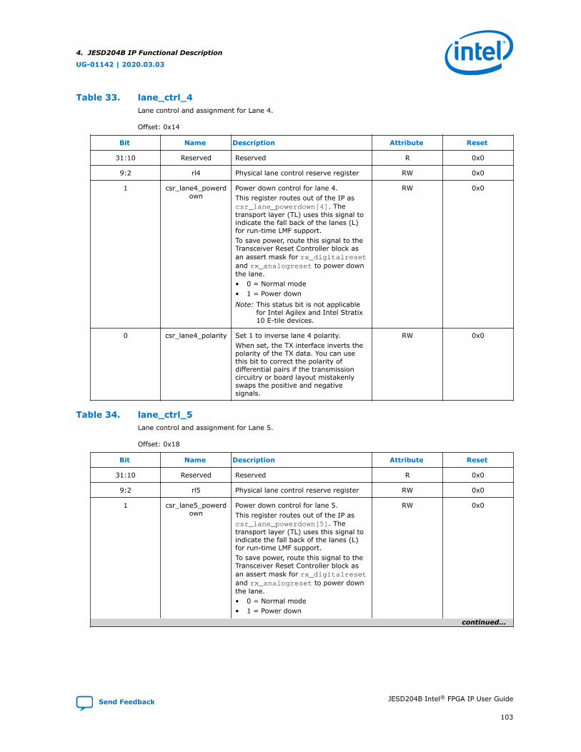
Table 33. lane_ctrl_4Lane control and assignment for Lane 4.
Offset: 0x14
Bit Name Description Attribute Reset
31:10 Reserved Reserved R 0x0
9:2 rl4 Physical lane control reserve register RW 0x0
1 csr_lane4_powerdown
Power down control for lane 4.This register routes out of the IP ascsr_lane_powerdown[4]. Thetransport layer (TL) uses this signal toindicate the fall back of the lanes (L)for run-time LMF support.To save power, route this signal to theTransceiver Reset Controller block asan assert mask for rx_digitalresetand rx_analogreset to power downthe lane.• 0 = Normal mode• 1 = Power downNote: This status bit is not applicable
for Intel Agilex and Intel Stratix10 E-tile devices.
RW 0x0
0 csr_lane4_polarity Set 1 to inverse lane 4 polarity.When set, the TX interface inverts thepolarity of the TX data. You can usethis bit to correct the polarity ofdifferential pairs if the transmissioncircuitry or board layout mistakenlyswaps the positive and negativesignals.
RW 0x0
Table 34. lane_ctrl_5Lane control and assignment for Lane 5.
Offset: 0x18
Bit Name Description Attribute Reset
31:10 Reserved Reserved R 0x0
9:2 rl5 Physical lane control reserve register RW 0x0
1 csr_lane5_powerdown
Power down control for lane 5.This register routes out of the IP ascsr_lane_powerdown[5]. Thetransport layer (TL) uses this signal toindicate the fall back of the lanes (L)for run-time LMF support.To save power, route this signal to theTransceiver Reset Controller block asan assert mask for rx_digitalresetand rx_analogreset to power downthe lane.• 0 = Normal mode• 1 = Power down
RW 0x0
continued...
4. JESD204B IP Functional Description
UG-01142 | 2020.03.03
Send Feedback JESD204B Intel® FPGA IP User Guide
103

Bit Name Description Attribute Reset
Note: This status bit is not applicablefor Intel Agilex and Intel Stratix10 E-tile devices.
0 csr_lane5_polarity Set 1 to inverse lane 5 polarity.When set, the TX interface inverts thepolarity of the TX data. You can usethis bit to correct the polarity ofdifferential pairs if the transmissioncircuitry or board layout mistakenlyswaps the positive and negativesignals.
RW 0x0
Table 35. lane_ctrl_6Lane control and assignment for Lane 6.
Offset: 0x1C
Bit Name Description Attribute Reset
31:10 Reserved Reserved R 0x0
9:2 rl6 Physical lane control reserve register RW 0x0
1 csr_lane6_powerdown
Power down control for lane 6.This register routes out of the IP ascsr_lane_powerdown[6]. Thetransport layer (TL) uses this signal toindicate the fall back of the lanes (L)for run-time LMF support.To save power, route this signal to theTransceiver Reset Controller block asan assert mask for rx_digitalresetand rx_analogreset to power downthe lane.• 0 = Normal mode• 1 = Power downNote: This status bit is not applicable
for Intel Agilex and Intel Stratix10 E-tile devices.
RW 0x0
0 csr_lane6_polarity Set 1 to inverse lane 6 polarity.When set, the TX interface inverts thepolarity of the TX data. You can usethis bit to correct the polarity ofdifferential pairs if the transmissioncircuitry or board layout mistakenlyswaps the positive and negativesignals.
RW 0x0
Table 36. lane_ctrl_7Lane control and assignment for Lane 7.
Offset: 0x20
Bit Name Description Attribute Reset
31:10 Reserved Reserved R 0x0
9:2 rl7 Physical lane control reserve register RW 0x0
1 csr_lane7_powerdown
Power down control for lane 7. RW 0x0
continued...
4. JESD204B IP Functional Description
UG-01142 | 2020.03.03
JESD204B Intel® FPGA IP User Guide Send Feedback
104

Bit Name Description Attribute Reset
This register routes out of the IP ascsr_lane_powerdown[7]. Thetransport layer (TL) uses this signal toindicate the fall back of the lanes (L)for run-time LMF support.To save power, route this signal to theTransceiver Reset Controller block asan assert mask for rx_digitalresetand rx_analogreset to power downthe lane.• 0 = Normal mode• 1 = Power downNote: This status bit is not applicable
for Intel Agilex and Intel Stratix10 E-tile devices.
0 csr_lane7_polarity Set 1 to inverse lane 7 polarity.When set, the TX interface inverts thepolarity of the TX data. You can usethis bit to correct the polarity ofdifferential pairs if the transmissioncircuitry or board layout mistakenlyswaps the positive and negativesignals.
RW 0x0
Table 37. dll_ctrlData link layer (DLL) and TX control.
Offset: 0x50
Bit Name Description Attribute Reset
31:17 Reserved Reserved R 0x0
16 rd5 DLL control reserve register 5 RW 0x0
15 rd4 DLL control reserve register 4 RW 0x0
14 rd3 DLL control reserve register 3 RW 0x0
13 rd2 DLL control reserve register 2 RW 0x0
12 rd1 DLL control reserve register 1 RW 0x0
11 csr_reinit_rxsyncn_rise
Control CGS state exit behavior duringlink reinitialization throughsyncn_sysref_ctrl (0x54)csr_link_reinit.
RW 0x0
continued...
4. JESD204B IP Functional Description
UG-01142 | 2020.03.03
Send Feedback JESD204B Intel® FPGA IP User Guide
105

Bit Name Description Attribute Reset
• 0 = Exit CGS state without detectedSYNC~ rise from DAC converter.(Default)If this mode is entered, transmittershall transmit at least four /K28.5/symbols and exit CGS state at nextLMFC boundary during link re-initialization.
• 1 = Exit CGS state only whendetected SYNC~ rise from DACconverter.If this mode is entered, transmittershall stays at CGS state andtransmit /K28.5/ symbols untildetected SYNC~ rise then exit CGSstate at next LMFC boundary duringlink re-initialization.
10 test_ilas_loop Write 1 to this register will force thestate machine to stay in Initial LaneAlignment Sequence (ILAS) stateindefinitely after entry. ILASConfiguration will be transmittedduring the second ILAS multiframe.The rest of the multiframe will have thestart-of-multiframe character (/R/)followed by dummy data and end-of-multiframe (/A/).There are 2 modes of entry perJESD204B Specification, chapter5.3.3.8.2:• If this mode is entered when
receiver initiates synchronizationrequest, transmitter shall initiateCGS. Upon completion of CGS,transmitter shall repeatedlytransmit ILAS.
• If there is no synchronizationrequest upon test entry, transmittershall transmit at least four /K28.5/symbols. At the LMFC boundary, thetransmitter shall repeatedlytransmit ILAS.
RW 0x0
9 csr_char_repl_disable
Disable character replacement fordebug purposes.When this bit is set, end-of-frame (/F/)and end-of-multiframe (/A/) characterreplacement will be disabled.• 0 = Character replacement enabled
(Default)• 1 = Character replacement
disabled. Used for debug purposes.
RW 0x0
8:1 csr_ilas_multiframe
The counter is binary value minus 1.ILAS required by subclass 1 and 2consists of exactly 4 multiframes.However, configurations with multiplesubclass 0 DAC devices may requireadditional multiframes to achieve lanealignment.Therefore, the length of ILAS shall beprogrammable from 4 up to 256multiframes. When illegal values like0/1/2 is set, the IP will still run as 4multiframes.
RW 0x0
continued...
4. JESD204B IP Functional Description
UG-01142 | 2020.03.03
JESD204B Intel® FPGA IP User Guide Send Feedback
106

Bit Name Description Attribute Reset
Note: This counter value takes effectregardless of subclass setting.Do not to change this registerfor Subclass 1 and Subclass 2.
0 csr_lane_sync_en Lane synchronization enable isrequired multilane alignment for aJESD204B link.• 0 = Lane synchronization is
disabled. ILAS will be bypassed.The character replacement of userdata during end of multiframe willbe considered as end of frame.
• 1 = Lane synchronization enabled(Default)
Note: For device that is classified asNMCDA-SL, you can disablelane synchronization. Set thisbit to 1 for all other devices.
RW 0x0
Table 38. syncn_sysref_ctrlSYNC_N and SYSREF control. Controls event sequencing related to SYNC_N and SYSREF signals.
Offset: 0x54
Bit Name Description Attribute Reset
31:21 Reserved Reserved R 0x0
20 csr_cgs_bypass_sysref
This bit applies to Subclass 1 only.Enabling DLL states transition fromCode Group Synchronization (CGS) toInitial Lane Alignment Sequence (ILAS)to bypass SYSREF single detectsampling. By default, the JESD204B IPwill remain in CGS state until SYSREFis sampled. Oncecsr_sysref_singledet is cleared,then only the DLL state can transitionfrom CGS to ILAS on the next LMFCtick.Write 1 to this register to allow the IPto exit out of CGS state withoutensuring that at least one rising edgeof SYSREF was sampled.Note: This is a debug mode, where
you can bypass SYSREFsampling if only a quick link upis required. Setting this bit to 1may cause race conditionbetween SYSREF sampling andCGS exit.
RW 0x0
19:12 csr_lmfc_offset The Local Multiframe Clock (LMFC)offset is a binary value minus 1.Upon the detection of the rising edgeof SYSREF in continuous mode orsingle detect mode, the LMFC counterwill be reset to the value set incsr_lmfc_offset.
RW 0x0
continued...
4. JESD204B IP Functional Description
UG-01142 | 2020.03.03
Send Feedback JESD204B Intel® FPGA IP User Guide
107

Bit Name Description Attribute Reset
The LMFC counter operates in linkclock domain, therefore the legal valuefor the counter is from 0 to ((FxK/4)-1.If you set an out-of-range value, theLMFC offset internally resets to 0.Note: By default, the rising edge of
SYSREF will reset the LMFCcounter to 0. However, if thesystem design has large phaseoffset between the SYSREFsampled by the converterdevice and the FPGA, you canvirtually shift the SYSREF edgesby changing the LMFC offsetreset value using this register.
11:7 Reserved Reserved R 0x0
6 rs4 SYNCN and SYSREF control reserveregister 4
RW 0x0
5 rs3 SYNCN and SYSREF control reserveregister 3
RW 0x0
4 rs2 SYNCN and SYSREF control reserveregister 2
RW 0x0
3 rs1 SYNCN and SYSREF control reserveregister 1
RW 0x0
2 csr_sysref_singledet
This register enables LMFC realignmentwith a single sample of rising edge ofSYSREF. The bit is auto-cleared byhardware once SYSREF is sampled. Ifyou require SYSREF to be sampledagain (due to link reset orreinitialization), you must set this bitagain.This register also has another criticalfunction. The JESD204B IP will neverwill never exit out of CGS unless atleast a SYSREF edge is sampled. Thisis to prevent race condition betweenSYSREF being sampled and the exit ofCGS to ILAS. If CGS transition to ILASbefore the common SYSREF is sampledfor both the IP and converter device,this would cause undeterministiclatency as the transmitted ILAS isbased on the free running LMFCcounter coming out of reset.• 0 = Any rising edge of SYSREF will
not reset the LMFC counter.• 1 = Resets the LMFC counter on the
first rising edge of SYSREF andthen clears this bit. (Default)
RW 0x1
continued...
4. JESD204B IP Functional Description
UG-01142 | 2020.03.03
JESD204B Intel® FPGA IP User Guide Send Feedback
108

Bit Name Description Attribute Reset
Note: Intel recommends that you usecsr_sysref_singledet withcsr_sysref_alwayson evenif you want to do SYSREFcontinuous detection mode.This is because this register isable to indicate whetherSYSREF was ever sampled. Thisregister also prevents racecondition as mentioned above.Using only SYSREF singledetect mode will not be able todetect incorrect SYSREF period.
1 csr_sysref_alwayson
This register enables LMFC realignmentat every rising edge of SYSREF. LMFCcounter is reset when every SYSREFtransition from 0 to 1 is detected.• 0 = Any rising edge of SYSREF will
not reset the LMFC counter.• 1 = Continuously resets LMFC
counter at every SYSREF risingedge.
Note: When this bit is set, theSYSREF period will be checkedto ensure it never violatesinternal local multiframe periodand this period can only be n-integer multiplied of ((FxK)/4.If the SYSREF period isdifferent from the localmultiframe period, tx_err(0x60)csr_sysref_lmfc_err will beasserted and an interrupt willbe triggered.
If you want to change SYSREF period,this bit should be set to 0 first. AfterSYSREF clock has stabilized, this bit isset to 1 to sample the rising edges ofthe new SYSREF.
RW 0x0
0 csr_link_reinit The JESD204B IP will reinitialize thelink to enter Code GroupSynchronization by transmitting /K28.5. The software will need to checkthat SYNC_N tx_status0 (0x80)csr_dev_syncn is 1 before settingthis register.This bit automatically clears once linkreinitialization is entered by hardware.• 0 = No link reinit request (Default)• 1 = Reinitialize the link.
RW 0x0
4. JESD204B IP Functional Description
UG-01142 | 2020.03.03
Send Feedback JESD204B Intel® FPGA IP User Guide
109

Table 39. tx_errThis register logs errors detected in the FPGA IP. Each set bit in the register will generate interrupt, if enabledby corresponding bits in the TX Error Enable (tx_err_enable (0x64)). After servicing the interrupt, the softwaremust clear the appropriate serviced interrupt status bit and ensure that no other interrupts are pending.
Offset: 0x60
Bit Name Description Attribute Reset
31:9 Reserved Reserved R 0x0
8 re4 TX error reserve status 4 RW 0x0
7 csr_pcfifo_empty_err
Detected 1 or more lanes of PhaseCompensation FIFO is emptyunexpectedly when the JESD204B linkis running.Note: This status bit is not applicable
for Intel Agilex and Intel Stratix10 devices.
Note: You MUST reset the JESD204Blink if this bit is triggered. Thetransceiver channel, and the IPlink reset must be applied.
RW1C 0x0
6 csr_pcfifo_full_err Detected 1 or more lanes of PhaseCompensation FIFO is full unexpectedlywhen the JESD204B link is running.Note: This status bit is not applicable
for Intel Agilex and Intel Stratix10 devices.
Note: You MUST reset the JESD204Blink if this bit is triggered. Thetransceiver channel, and the IPlink reset must be applied.
RW1C 0x0
5 csr_pll_locked_err Detected 1 or more lanes of PLL lockedloose lock when the JESD204B link isrunning.Note: This status bit is not applicable
for Intel Agilex and Intel Stratix10 E-tile devices.
RW1C 0x0
4 csr_syncn_reinit_req
Receiver has requested reinitializationby asserting SYNC_N low for more than5 frames and 9 octets.Note: Upon the detection of SYNC_N
link reinitialization request fromthe receiver, the JESD204B IPenters Code GroupSynchronization (CGS) andtransmits continuous /K28.5/. Ifyou want to regenerate andsample SYSREF, enabling thisinterrupt notifies the softwarethat the receiver has requestedfor link reinitialization.
RW1C 0x0
3 csr_frame_data_invalid_err
This error bit is applicable only if youuse the Intel FPGA transport layer inyour design. This error bit will beasserted if the upstream componentdeasserts thejesd204_tx_data_valid signal atthe Intel FPGA transport layer AV-STbus.
RW1C 0x0
continued...
4. JESD204B IP Functional Description
UG-01142 | 2020.03.03
JESD204B Intel® FPGA IP User Guide Send Feedback
110

Bit Name Description Attribute Reset
The transport layer expects theupstream device in the system toalways send the valid data with zerolatency whenjesd204_tx_data_ready is assertedby the transport layer.Note: If this error detection is not
required, you can tie off thejesd204_tx_frame_errorsignal to 0.
2 csr_dll_data_invalid_err
This error bit will be asserted if the TXdetects data invalid on the AV-ST buswhen data is requested.By design, the JESD204B TX coreexpects the upstream device(JESD204B transport layer) to alwayssend the valid data with zero latencywhen jesd204_tx_data_ready isasserted.Note: If this error detection is not
required, you can tie off thejesd204_tx_link_validsignal to 1.
RW1C 0x0
1 csr_sysref_lmfc_err
When syncn_sysref_ctrl (0x54)csr_sysref_alwayson is set to 1,the LMFC counter checks whether theSYSREF period matches the LMFCcounter where it is n-integer multiplierof the (FxK/4).If SYSREF period does not match theLMFC period, this bit will be asserted.
RW1C 0x0
0 csr_syncn_err The JESD204B receiver indicates errorthrough the SYNC_N signal.
RW1C 0x0
Table 40. tx_err_enableThis register enables the error types that will generate interrupt. Setting 0 to the register bits will disable thespecific error type from generating interrupt.
Offset: 0x64
Bit Name Description Attribute Reset
31:9 Reserved Reserved R 0x0
8 re4_en TX error enable reserve 4 RW 0x1
7 csr_pcfifo_empty_err_en
Enable interrupt for PhaseCompensation FIFO empty error
RW 0x1
6 csr_pcfifo_full_err_en
Enable interrupt for PhaseCompensation FIFO full error
RW 0x1
5 csr_pll_locked_err_en
Enable interrupt for PLL loose lockerror.Note: This status bit is not applicable
for Intel Agilex and Intel Stratix10 E-tile devices.
RW 0x1
4 csr_syncn_reinit_req_en
Enable interrupt for SYNCN reinitrequest.
RW 0x1
continued...
4. JESD204B IP Functional Description
UG-01142 | 2020.03.03
Send Feedback JESD204B Intel® FPGA IP User Guide
111
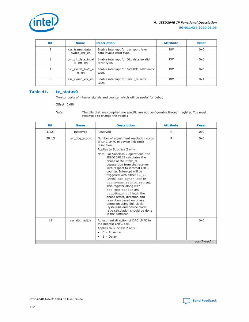
Bit Name Description Attribute Reset
3 csr_frame_data_invalid_err_en
Enable interrupt for transport layerdata invalid error type.
RW 0x0
2 csr_dll_data_invalid_err_en
Enable interrupt for DLL data invaliderror type.
RW 0x0
1 csr_sysref_lmfc_err_en
Enable interrupt for SYSREF LMFC errortype.
RW 0x0
0 csr_syncn_err_en Enable interrupt for SYNC_N errortype.
RW 0x1
Table 41. tx_status0Monitor ports of internal signals and counter which will be useful for debug.
Offset: 0x80
Note: The bits that are compile-time specific are not configurable through register. You mustrecompile to change the value.)
Bit Name Description Attribute Reset
31:21 Reserved Reserved R 0x0
20:13 csr_dbg_adjcnt Number of adjustment resolution stepsof DAC LMFC in device link clockresolution.Applies to Subclass 2 only.Note: For Subclass 2 operations, the
JESD204B IP calculates thephase of the SYNC_Ndeassertion from the receiverwith respect to internal LMFCcounter. Interrupt will betriggered with either tx_err(0x60) csr_syncn_err orcsr_syncn_reinit_req set.This register along withcsr_dbg_adjdir andcsr_dbg_phadj latch thephase offset, direction andresolution based on phasedetection using link clock.Hysteresis and device clockratio calculation should be donein the software.
R 0x0
12 csr_dbg_adjdir Adjustment direction of DAC LMFC tothe nearest LMFC tick.Applies to Subclass 2 only.• 0 = Advance• 1 = Delay
0x0
continued...
4. JESD204B IP Functional Description
UG-01142 | 2020.03.03
JESD204B Intel® FPGA IP User Guide Send Feedback
112

Bit Name Description Attribute Reset
Note: For Subclass 2 operations, theJESD204B IP calculates thephase of the SYNC_Ndeassertion from the receiverwith respect to internal LMFCcounter. Interrupt will betriggered with either tx_err(0x60) csr_syncn_err orcsr_syncn_reinit_req set.This register along withcsr_dbg_phadj andcsr_dbg_adjcnt latch thephase offset, direction andresolution based on phasedetection using link clock.Hysteresis and device clockratio calculation should be donein the software.
11 csr_dbg_phadj SYNC_N deassertion is not-in-phasewith the internal LMFC counter.Applies to Subclass 2 only.• 0 = DAC LMFC is aligned to device
LMFC.• 1 = DAC LMFC is NOT aligned to
device LMFCNote: For Subclass 2 operations, the
JESD204B IP calculates thephase of the SYNC_Ndeassertion from the receiverwith respect to internal LMFCcounter. Interrupt will betriggered with either tx_err(0x60) csr_syncn_err orcsr_syncn_reinit_req set.This register along withcsr_dbg_adjdir andcsr_dbg_adjcnt latch thephase offset, direction andresolution based on phasedetection using link clock.Hysteresis and device clockratio calculation should be donein the software.
0x0
10:3 csr_ilas_cnt This register is a binary minus 1 value.The counter value reflects on whichnumber of ILAS multiframe the DLLstate machine is in.
R 0x0
2 csr_dll_state Current state of data link layer (DLL).• 00 = Code Group Synchronization
(CGS)• 01 = Initial Lane Alignment
Sequence (ILAS)• 10 = User Data Mode• 11 = D21.5 test mode
R 0x0
1:0 csr_dev_syncn Internal SYNC_N value.• 0 = Receiver is asserting
synchronization request.• 1 = JESD204B link is out of
synchronization.
R 0x0
4. JESD204B IP Functional Description
UG-01142 | 2020.03.03
Send Feedback JESD204B Intel® FPGA IP User Guide
113

Table 42. tx_status1Monitor ports of internal signals and counter which will be useful for debug.
Offset: 0x84
Bit Name Description Attribute Reset
31:24 Reserved Reserved R 0x0
23 csr_lane7_tx_pcfifo_empty
TX phase compensation FIFO statusempty flag for lane 7
R 0x0
22 csr_lane6_tx_pcfifo_empty
TX phase compensation FIFO statusempty flag for lane 6
R 0x0
21 csr_lane5_tx_pcfifo_empty
TX phase compensation FIFO statusempty flag for lane 5
R 0x0
20 csr_lane4_tx_pcfifo_empty
TX phase compensation FIFO statusempty flag for lane 4
R 0x0
19 csr_lane3_tx_pcfifo_empty
TX phase compensation FIFO statusempty flag for lane 3
R 0x0
18 csr_lane2_tx_pcfifo_empty
TX phase compensation FIFO statusempty flag for lane 2
R 0x0
17 csr_lane1_tx_pcfifo_empty
TX phase compensation FIFO statusempty flag for lane 1
R 0x0
16 csr_lane0_tx_pcfifo_empty
TX phase compensation FIFO statusempty flag for lane 0
R 0x0
15:8 Reserved Reserved R 0x0
7 csr_lane7_tx_pcfifo_full
TX phase compensation FIFO status fullflag for lane 7
R 0x0
6 csr_lane6_tx_pcfifo_full
TX phase compensation FIFO status fullflag for lane 6
R 0x0
5 csr_lane5_tx_pcfifo_full
TX phase compensation FIFO status fullflag for lane 5
R 0x0
4 csr_lane4_tx_pcfifo_full
TX phase compensation FIFO status fullflag for lane 4
R 0x0
3 csr_lane3_tx_pcfifo_full
TX phase compensation FIFO status fullflag for lane 3
R 0x0
2 csr_lane2_tx_pcfifo_full
TX phase compensation FIFO status fullflag for lane 2
R 0x0
1 csr_lane1_tx_pcfifo_full
TX phase compensation FIFO status fullflag for lane 1
R 0x0
0 csr_lane0_tx_pcfifo_full
TX phase compensation FIFO status fullflag for lane 0
R 0x0
Table 43. tx_status2Monitor ports of internal signals and counter which will be useful for debug.
Offset: 0x88
Bit Name Description Attribute Reset
31:24 Reserved Reserved R 0x0
23 csr_lane7_pll_locked
PLL status for lane 7, indicates PLL islocked.
R 0x0
continued...
4. JESD204B IP Functional Description
UG-01142 | 2020.03.03
JESD204B Intel® FPGA IP User Guide Send Feedback
114

Bit Name Description Attribute Reset
For Intel Agilex and Intel Stratix 10 E-tile devices, tie this register to 1’b1.
22 csr_lane6_pll_locked
PLL status for lane 6, indicates PLL islocked.For Intel Agilex and Intel Stratix 10 E-tile devices, tie this register to 1’b1.
R 0x0
21 csr_lane5_pll_locked
PLL status for lane 5, indicates PLL islocked.For Intel Agilex and Intel Stratix 10 E-tile devices, tie this register to 1’b1.
R 0x0
20 csr_lane4_pll_locked
PLL status for lane 4, indicates PLL islocked.For Intel Agilex and Intel Stratix 10 E-tile devices, tie this register to 1’b1.
R 0x0
19 csr_lane3_pll_locked
PLL status for lane 3, indicates PLL islocked.For Intel Agilex and Intel Stratix 10 E-tile devices, tie this register to 1’b1.
R 0x0
18 csr_lane2_pll_locked
PLL status for lane 2, indicates PLL islocked.For Intel Agilex and Intel Stratix 10 E-tile devices, tie this register to 1’b1.
R 0x0
17 csr_lane1_pll_locked
PLL status for lane 1, indicates PLL islocked.For Intel Agilex and Intel Stratix 10 E-tile devices, tie this register to 1’b1.
R 0x0
16 csr_lane0_pll_locked
PLL status for lane 0, indicates PLL islocked.For bonded mode, the transceivergenerates only one PLL locked signal.The single bit will be routed to lane 0of PLL locked status. All other lanes willbe tied off to 0.For non-bonded mode, PLL lockedstatus will be per channel. The statuswill be routed to the respective PLLlocked status per channel.For Intel Agilex and Intel Stratix 10 E-tile devices, tie this register to 1’b1.
R 0x0
15:8 Reserved Reserved R 0x0
7 csr_lane7_tx_cal_busy
Reconfig status for lane 7, indicates TXcalibration is in progress.Note: This status bit is not applicable
for Intel Agilex and Intel Stratix10 E-tile devices.
R 0x0
6 csr_lane6_tx_cal_busy
Reconfig status for lane 6, indicates TXcalibration is in progress.Note: This status bit is not applicable
for Intel Agilex and Intel Stratix10 E-tile devices.
R 0x0
5 csr_lane5_tx_cal_busy
Reconfig status for lane 5, indicates TXcalibration is in progress.Note: This status bit is not applicable
for Intel Agilex and Intel Stratix10 E-tile devices.
R 0x0
continued...
4. JESD204B IP Functional Description
UG-01142 | 2020.03.03
Send Feedback JESD204B Intel® FPGA IP User Guide
115

Bit Name Description Attribute Reset
4 csr_lane4_tx_cal_busy
Reconfig status for lane 4, indicates TXcalibration is in progress.Note: This status bit is not applicable
for Intel Agilex and Intel Stratix10 E-tile devices.
R 0x0
3 csr_lane3_tx_cal_busy
Reconfig status for lane 3, indicates TXcalibration is in progress.Note: This status bit is not applicable
for Intel Agilex and Intel Stratix10 E-tile devices.
R 0x0
2 csr_lane2_tx_cal_busy
Reconfig status for lane 2, indicates TXcalibration is in progress.Note: This status bit is not applicable
for Intel Agilex and Intel Stratix10 E-tile devices.
R 0x0
1 csr_lane1_tx_cal_busy
Reconfig status for lane 1, indicates TXcalibration is in progress.Note: This status bit is not applicable
for Intel Agilex and Intel Stratix10 E-tile devices.
R 0x0
0 csr_lane0_tx_cal_busy
Reconfig status for lane 0, indicates TXcalibration is in progress.Note: This status bit is not applicable
for Intel Agilex and Intel Stratix10 E-tile devices.
.
R 0x0
Table 44. tx_status3TX status reserve..
Offset: 0x8C
Bit Name Description Attribute Reset
31:0 rs32 TX status reserve. R 0x0
Table 45. ilas_data1Link control configuration transmitted during initial lane alignment sequence (ILAS).
Offset: 0x94
Bit Name Description Attribute Reset
31:24 csr_m Link M.Number of converters per device(binary value minus 1).Note: Run-time reconfiguration is
disabled for Intel Agilex andIntel Stratix 10 devices.
• RW for alldevices exceptIntel Agilexand IntelStratix 10
• RO for IntelAgilex andIntel Stratix 10devices
Reset toparameter valueper IP generation.
23:21 Reserved Reserved R 0x0
continued...
4. JESD204B IP Functional Description
UG-01142 | 2020.03.03
JESD204B Intel® FPGA IP User Guide Send Feedback
116

Bit Name Description Attribute Reset
20:16 csr_k Link K.Number of frames per multiframe(binary value minus 1).A multiframe is defined as a group of Ksuccessive frames where K is between1 and 32 and such that the number ofoctets per multiframe is between 17and 1024. The IP requires that FxKmust be divisible by 4.Note: Run-time reconfiguration is
disabled for Intel Agilex andIntel Stratix 10 devices.
• RW for alldevices exceptIntel Agilexand IntelStratix 10
• RO for IntelAgilex andIntel Stratix 10devices
Reset toparameter valueper IP generation.
15:8 csr_f Link F.Number of octets per frame (binaryvalue minus 1).Note: Run-time reconfiguration is
disabled for Intel Agilex andIntel Stratix 10 devices.
• RW for alldevices exceptIntel Agilexand IntelStratix 10
• RO for IntelAgilex andIntel Stratix 10devices
Reset toparameter valueper IP generation.
7 csr_scr_en Enable or disable descrambler.• 0 = Disable descrambler• 1 = Enable descramblerNote: Run-time reconfiguration is
disabled for Intel Agilex andIntel Stratix 10 devices.
.
• RW for alldevices exceptIntel Agilexand IntelStratix 10
• RO for IntelAgilex andIntel Stratix 10devices
Reset toparameter valueper IP generation.
6:5 Reserved Reserved R 0x0
4:0 csr_l Link L.Number of lanes per converter (binaryvalue minus 1).Note: Run-time reconfiguration is
disabled for Intel Agilex andIntel Stratix 10 devices.
• RW for alldevices exceptIntel Agilexand IntelStratix 10
• RO for IntelAgilex andIntel Stratix 10devices
Reset toparameter valueper IP generation.
Table 46. ilas_data2Link control configuration transmitted during initial lane alignment sequence (ILAS).
Offset: 0x98
Bit Name Description Attribute Reset
31 csr_hd Link HD.High density format.Note: Run-time reconfiguration is
disabled for Intel Agilex andIntel Stratix 10 devices.
• RW for alldevices exceptIntel Agilexand IntelStratix 10
• RO for IntelAgilex andIntel Stratix 10devices
Reset toparameter valueper IP generation.
30:29 Reserved Reserved R 0x0
continued...
4. JESD204B IP Functional Description
UG-01142 | 2020.03.03
Send Feedback JESD204B Intel® FPGA IP User Guide
117

Bit Name Description Attribute Reset
28:24 csr_cf Link CF.Number of control words per frameclock period per link• CF = L is encoded as 31: control
words on all lanes.• CF = 31 can only occur when L =
31Note: Run-time reconfiguration is
disabled for Intel Agilex andIntel Stratix 10 devices.
• RW for alldevices exceptIntel Agilexand IntelStratix 10
• RO for IntelAgilex andIntel Stratix 10devices
Reset toparameter valueper IP generation.
23:21 csr_jesdv JESD204x version.• 000 = JESD204A• 001 = JESD204BNote: Run-time reconfiguration is
disabled for Intel Stratix 10devices.
• RW for alldevices exceptIntel Stratix 10
• RO for IntelStratix 10devices
0x1
20:16 csr_s Link S.Number of samples per converter perframe cycle (binary value minus 1).Note: Run-time reconfiguration is
disabled for Intel Stratix 10devices.
• RW for alldevices exceptIntel Agilexand IntelStratix 10
• RO for IntelAgilex andIntel Stratix 10devices
Reset toparameter valueper IP generation.
15:13 csr_subclassv Device subclass version• 000 = Subclass 0• 001 = Subclass 1• 010 = Subclass 2Note: Run-time reconfiguration is
disabled for Intel Agilex andIntel Stratix 10 devices.
• RW for alldevices exceptIntel Agilexand IntelStratix 10
• RO for IntelAgilex andIntel Stratix 10devices
Reset toparameter valueper IP generation.
12.8 csr_np Link NP.Total number of bits per sample(binary value minus 1).Note: Run-time reconfiguration is
disabled for Intel Agilex andIntel Stratix 10 devices.
• RW for alldevices exceptIntel Agilexand IntelStratix 10
• RO for IntelAgilex andIntel Stratix 10devices
Reset toparameter valueper IP generation.
continued...
4. JESD204B IP Functional Description
UG-01142 | 2020.03.03
JESD204B Intel® FPGA IP User Guide Send Feedback
118

Bit Name Description Attribute Reset
7:6 csr_cs Link CS.Number of control bits per sample.Note: Run-time reconfiguration is
disabled for Intel Agilex andIntel Stratix 10 devices.
• RW for alldevices exceptIntel Agilexand IntelStratix 10
• RO for IntelAgilex andIntel Stratix 10devices
Reset toparameter valueper IP generation.
5 Reserved Reserved R 0x0
4:0 csr_n Link N.Converter resolution (binary valueminus 1).Note: Run-time reconfiguration is
disabled for Intel Agilex andIntel Stratix 10 devices.
• RW for alldevices exceptIntel Agilexand IntelStratix 10
• RO for IntelAgilex andIntel Stratix 10devices
Reset toparameter valueper IP generation.
Table 47. ilas_data3Link control configuration transmitted during initial lane alignment sequence (ILAS).
Offset: 0x9C
Bit Name Description Attribute Reset
31 csr_phadj Phase adjustment request of DACLMFC. The register is auto-cleared bythe hardware after sending ILAS 2ndmultiframe.Applies to Subclass 2 only.
RW Reset toparameter valueper IP generation.
30 csr_adjdir Adjustment direction of DAC LMFC. Theregister is auto-cleared by thehardware after sending ILAS 2ndmultiframe.Applies to Subclass 2 only.• 0 = Advance• 1 = Delay
RW Reset toparameter valueper IP generation.
29:20 Reserved Reserved R 0x0
19:16 csr_f Number of adjustment resolution stepsof DAC LMFC. The register is auto-cleared by the hardware after sendingILAS 2nd multiframe.Applies to Subclass 2 only.
RW Reset toparameter valueper IP generation.
15:8 csr_rsvd2 ILAS reserved 2 bytes. RW 0x00
7:0 csr_rsvd1 ILAS reserved 1 bytes. RW 0x00
4. JESD204B IP Functional Description
UG-01142 | 2020.03.03
Send Feedback JESD204B Intel® FPGA IP User Guide
119

Table 48. ilas_data4Link control configuration transmitted during initial lane alignment sequence (ILAS).
Offset: 0xA0
Bit Name Description Attribute Reset
31:29 Reserved Reserved R 0x0
28:24 csr_lid_l3 Lane Identification for lane 3transmitted during ILAS.
RW Reset toparameter valueper IP generation.
23:21 Reserved Reserved R 0x0
20:16 csr_lid_l2 Lane Identification for lane 2transmitted during ILAS.
RW Reset toparameter valueper IP generation.
15:13 Reserved Reserved R 0x0
12:8 csr_lid_l1 Lane Identification for lane 1transmitted during ILAS.
RW Reset toparameter valueper IP generation.
7:5 Reserved Reserved R 0x0
4:0 csr_lid_l0 Lane Identification for lane 0transmitted during ILAS.
RW Reset toparameter valueper IP generation.
Table 49. ilas_data5Link control configuration transmitted during initial lane alignment sequence (ILAS).
Offset: 0xA4
Bit Name Description Attribute Reset
31:29 Reserved Reserved R 0x0
28:24 csr_lid_l7 Lane Identification for lane 7transmitted during ILAS.
RW Reset toparameter valueper IP generation.
23:21 Reserved Reserved R 0x0
20:16 csr_lid_l6 Lane Identification for lane 6transmitted during ILAS.
RW Reset toparameter valueper IP generation.
15:13 Reserved Reserved R 0x0
12:8 csr_lid_l5 Lane Identification for lane 5transmitted during ILAS.
RW Reset toparameter valueper IP generation.
7:5 Reserved Reserved R 0x0
4:0 csr_lid_l4 Lane Identification for lane 4transmitted during ILAS.
RW Reset toparameter valueper IP generation.
4. JESD204B IP Functional Description
UG-01142 | 2020.03.03
JESD204B Intel® FPGA IP User Guide Send Feedback
120

Table 50. ilas_data8Link control configuration transmitted during initial lane alignment sequence (ILAS).
Offset: 0xB0
Bit Name Description Attribute Reset
31:24 csr_fchk_l3 ILAS checksum lane 3. Checksum isthe modulo 256 of parameters listedILAS configuration data.
RW Reset toparameter valueper IP generation.
23:16 csr_fchk_l2 ILAS checksum lane 2. Checksum isthe modulo 256 of parameters listedILAS configuration data.
RW Reset toparameter valueper IP generation.
15:8 csr_fchk_l1 ILAS checksum lane 1. Checksum isthe modulo 256 of parameters listedILAS configuration data.
RW Reset toparameter valueper IP generation.
7:0 csr_fchk_l0 ILAS checksum lane 0. Checksum isthe modulo 256 of parameters listedILAS configuration data.
RW Reset toparameter valueper IP generation.
Table 51. ilas_data9Link control configuration transmitted during initial lane alignment sequence (ILAS).
Offset: 0xB4
Bit Name Description Attribute Reset
31:10 csr_fchk_l7 ILAS checksum lane 7. Checksum isthe modulo 256 of parameters listedILAS configuration data.
RW Reset toparameter valueper IP generation.
23:16 csr_fchk_l6 ILAS checksum lane 6. Checksum isthe modulo 256 of parameters listedILAS configuration data.
RW Reset toparameter valueper IP generation.
15:8 csr_fchk_l5 ILAS checksum lane 5. Checksum isthe modulo 256 of parameters listedILAS configuration data.
RW Reset toparameter valueper IP generation.
7:0 csr_fchk_l4 ILAS checksum lane 4. Checksum isthe modulo 256 of parameters listedILAS configuration data.
RW Reset toparameter valueper IP generation.
Table 52. ilas_data12Link control configuration transmitted during initial lane alignment sequence (ILAS).
Offset: 0xC0
Bit Name Description Attribute Reset
31:10 Reserved Reserved R 0x0
9:2 csr_fxk_h Upper bits of FxK[8:2]. This is a binaryvalue minus 1.Link F multiply with Link K must bedivisible by 4.Note: The IP runs on 32-bit data
width boundary per channel, soyou must always ensure thatFxK must be divisible by 4.
• RW for alldevices exceptIntel Agilexand IntelStratix 10
• RO for IntelAgilex andIntel Stratix 10devices
Reset toparameter valueper IP generation.
continued...
4. JESD204B IP Functional Description
UG-01142 | 2020.03.03
Send Feedback JESD204B Intel® FPGA IP User Guide
121
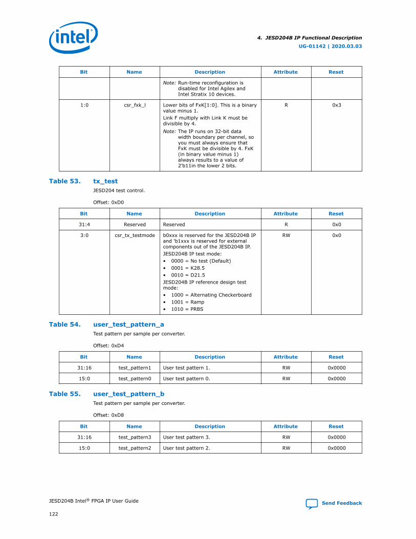
Bit Name Description Attribute Reset
Note: Run-time reconfiguration isdisabled for Intel Agilex andIntel Stratix 10 devices.
1:0 csr_fxk_l Lower bits of FxK[1:0]. This is a binaryvalue minus 1.Link F multiply with Link K must bedivisible by 4.Note: The IP runs on 32-bit data
width boundary per channel, soyou must always ensure thatFxK must be divisible by 4. FxK(in binary value minus 1)always results to a value of2'b11in the lower 2 bits.
R 0x3
Table 53. tx_testJESD204 test control.
Offset: 0xD0
Bit Name Description Attribute Reset
31:4 Reserved Reserved R 0x0
3:0 csr_tx_testmode b0xxx is reserved for the JESD204B IPand 'b1xxx is reserved for externalcomponents out of the JESD204B IP.JESD204B IP test mode:• 0000 = No test (Default)• 0001 = K28.5• 0010 = D21.5JESD204B IP reference design testmode:• 1000 = Alternating Checkerboard• 1001 = Ramp• 1010 = PRBS
RW 0x0
Table 54. user_test_pattern_aTest pattern per sample per converter.
Offset: 0xD4
Bit Name Description Attribute Reset
31:16 test_pattern1 User test pattern 1. RW 0x0000
15:0 test_pattern0 User test pattern 0. RW 0x0000
Table 55. user_test_pattern_bTest pattern per sample per converter.
Offset: 0xD8
Bit Name Description Attribute Reset
31:16 test_pattern3 User test pattern 3. RW 0x0000
15:0 test_pattern2 User test pattern 2. RW 0x0000
4. JESD204B IP Functional Description
UG-01142 | 2020.03.03
JESD204B Intel® FPGA IP User Guide Send Feedback
122

Table 56. user_test_pattern_cTest pattern per sample per converter.
Offset: 0xDC
Bit Name Description Attribute Reset
31:16 test_pattern5 User test pattern 5. RW 0x0000
15:0 test_pattern4 User test pattern 4. RW 0x0000
Table 57. user_test_pattern_dTest pattern per sample per converter.
Offset: 0xE0
Bit Name Description Attribute Reset
31:16 test_pattern7 User test pattern 7. RW 0x0000
15:0 test_pattern6 User test pattern 6. RW 0x0000
4.7.3. Receiver Registers
Table 58. lane_ctrl_commonCommon lane control and assignment. The common lane control applies to all lanes in the link.
Offset: 0x0
Note: The bits that are compile-time specific are not configurable through register. You mustrecompile to change the value.)
Bit Name Description Attribute Reset
31:3 Reserved Reserved R 0x0
2 rl Physical lane control reserve register RW 0x0
1 csr_bit_reversal Bit reversal for LSB/MSB firstserialization. This is a compile-timeoption which needs to be set before IPgeneration.• 0 = LSB-first serialization• 1 = MSB-first serializationNote: JESD204B converter device
may support either MSB-firstserialization or LSB-firstserialization.
You must set bothcsr_byte_reversal andcsr_bit_reversal bits to 1 whengenerating the IP.When csr_bit_reversal = 1, theword aligner reverses the RX paralleldata bits upon receiving the PMAdeserialized data.
R Compile-timespecific
continued...
4. JESD204B IP Functional Description
UG-01142 | 2020.03.03
Send Feedback JESD204B Intel® FPGA IP User Guide
123

Bit Name Description Attribute Reset
For example; in 20-bit mode; D[19:0]is rewired to D[0:19] and in 40-bitmode; D[39:0] is rewired to D[0:39].
0 csr_byte_reversal Byte reversal for LSB/MSB firstserialization. This is a compile-timeoption which needs to be set before IPgeneration.• 0 = LSB-first serialization
Byte order = {octet3, octet2,octet1, octet0}
• 1 = MSB-first serializationByte order = {octet0, octet1,octet2, octet3}
Note: JESD204B converter devicemay support either MSB-firstserialization or LSB-firstserialization.
When csr_byte_reversal = 1, theword aligner reverses the byte order.
R Compile-timespecific
Table 59. lane_ctrl_0Lane control and assignment for lane 0.
Offset: 0x4
Bit Name Description Attribute Reset
31:3 Reserved Reserved R 0x0
2 csr_alllanes_patternalign_en
Enables word alignment to thespecified pattern boundary alignmentduring link initialization. You should setthis bit to 1 in normal operations.Note: You can disable this bit to
debug bit slip error.
RW 0x1
1 csr_lane0_powerdown
Power down control for lane 0.This register routes out of the IP ascsr_lane_powerdown[0]. Thetransport layer (TL) uses this signal toindicate the fall back of the lanes (L)for run-time LMF support.To save power, route this signal to theTransceiver Reset Controller block asan assert mask for rx_digitalresetand rx_analogreset to power downthe lane.• 0 = Normal mode• 1 = Power down
RW 0x0
0 csr_lane0_polarity Set 1 to inverse lane 0 polarity.When set, the RX interface inverts thepolarity of the RX data. You can usethis bit to correct the polarity ofdifferential pairs if the transmissioncircuitry or board layout mistakenlyswaps the positive and negativesignals.
RW 0x0
4. JESD204B IP Functional Description
UG-01142 | 2020.03.03
JESD204B Intel® FPGA IP User Guide Send Feedback
124

Table 60. lane_ctrl_1Lane control and assignment for lane 1.
Offset: 0xC
Bit Name Description Attribute Reset
31:3 Reserved Reserved R 0x0
2 rl1 Physical lane control reserve register. RW 0x1
1 csr_lane1_powerdown
Power down control for lane 1.This register routes out of the IP ascsr_lane_powerdown[1]. Thetransport layer (TL) uses this signal toindicate the fall back of the lanes (L)for run-time LMF support.To save power, route this signal to theTransceiver Reset Controller block asan assert mask for rx_digitalresetand rx_analogreset to power downthe lane.• 0 = Normal mode• 1 = Power down
RW 0x0
0 csr_lane1_polarity Set 1 to inverse lane 1 polarity.When set, the RX interface inverts thepolarity of the RX data. You can usethis bit to correct the polarity ofdifferential pairs if the transmissioncircuitry or board layout mistakenlyswaps the positive and negativesignals.
RW 0x0
Table 61. lane_ctrl_2Lane control and assignment for lane 2.
Offset: 0xC
Bit Name Description Attribute Reset
31:3 Reserved Reserved R 0x0
2 rl2 Physical lane control reserve register. RW 0x1
1 csr_lane2_powerdown
Power down control for lane 2.This register routes out of the IP ascsr_lane_powerdown[2]. Thetransport layer (TL) uses this signal toindicate the fall back of the lanes (L)for run-time LMF support.To save power, route this signal to theTransceiver Reset Controller block asan assert mask for rx_digitalresetand rx_analogreset to power downthe lane.• 0 = Normal mode• 1 = Power down
RW 0x0
0 csr_lane2_polarity Set 1 to inverse lane 2 polarity.When set, the RX interface inverts thepolarity of the RX data. You can usethis bit to correct the polarity ofdifferential pairs if the transmissioncircuitry or board layout mistakenlyswaps the positive and negativesignals.
RW 0x0
4. JESD204B IP Functional Description
UG-01142 | 2020.03.03
Send Feedback JESD204B Intel® FPGA IP User Guide
125

Table 62. lane_ctrl_3Lane control and assignment for lane 3.
Offset: 0x10
Bit Name Description Attribute Reset
31:3 Reserved Reserved R 0x0
2 rl3 Physical lane control reserve register. RW 0x1
1 csr_lane3_powerdown
Power down control for lane 3.This register routes out of the IP ascsr_lane_powerdown[3]. Thetransport layer (TL) uses this signal toindicate the fall back of the lanes (L)for run-time LMF support.To save power, route this signal to theTransceiver Reset Controller block asan assert mask for rx_digitalresetand rx_analogreset to power downthe lane.• 0 = Normal mode• 1 = Power down
RW 0x0
0 csr_lane3_polarity Set 1 to inverse lane 3 polarity.When set, the RX interface inverts thepolarity of the RX data. You can usethis bit to correct the polarity ofdifferential pairs if the transmissioncircuitry or board layout mistakenlyswaps the positive and negativesignals.
RW 0x0
Table 63. lane_ctrl_4Lane control and assignment for lane 4.
Offset: 0x14
Bit Name Description Attribute Reset
31:3 Reserved Reserved R 0x0
2 rl4 Physical lane control reserve register. RW 0x1
1 csr_lane4_powerdown
Power down control for lane 4.This register routes out of the IP ascsr_lane_powerdown[4]. Thetransport layer (TL) uses this signal toindicate the fall back of the lanes (L)for run-time LMF support.To save power, route this signal to theTransceiver Reset Controller block asan assert mask for rx_digitalresetand rx_analogreset to power downthe lane.• 0 = Normal mode• 1 = Power down
RW 0x0
0 csr_lane4_polarity Set 1 to inverse lane 4 polarity.When set, the RX interface inverts thepolarity of the RX data. You can usethis bit to correct the polarity ofdifferential pairs if the transmissioncircuitry or board layout mistakenlyswaps the positive and negativesignals.
RW 0x0
4. JESD204B IP Functional Description
UG-01142 | 2020.03.03
JESD204B Intel® FPGA IP User Guide Send Feedback
126
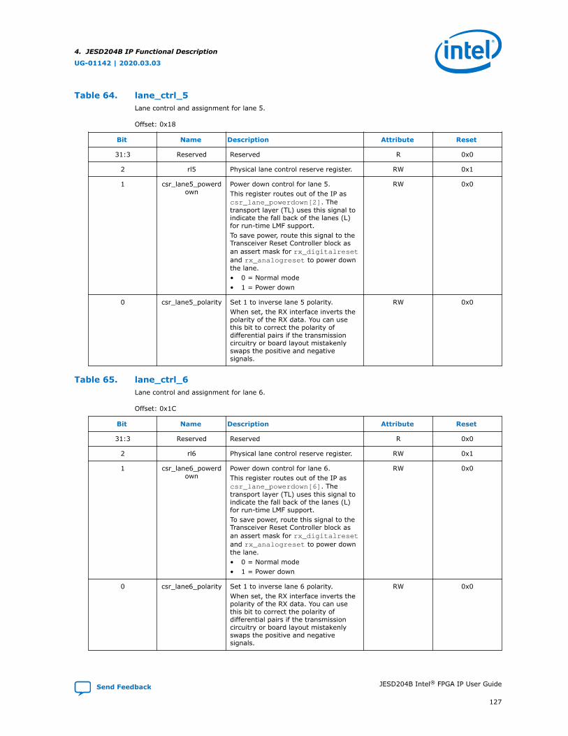
Table 64. lane_ctrl_5Lane control and assignment for lane 5.
Offset: 0x18
Bit Name Description Attribute Reset
31:3 Reserved Reserved R 0x0
2 rl5 Physical lane control reserve register. RW 0x1
1 csr_lane5_powerdown
Power down control for lane 5.This register routes out of the IP ascsr_lane_powerdown[2]. Thetransport layer (TL) uses this signal toindicate the fall back of the lanes (L)for run-time LMF support.To save power, route this signal to theTransceiver Reset Controller block asan assert mask for rx_digitalresetand rx_analogreset to power downthe lane.• 0 = Normal mode• 1 = Power down
RW 0x0
0 csr_lane5_polarity Set 1 to inverse lane 5 polarity.When set, the RX interface inverts thepolarity of the RX data. You can usethis bit to correct the polarity ofdifferential pairs if the transmissioncircuitry or board layout mistakenlyswaps the positive and negativesignals.
RW 0x0
Table 65. lane_ctrl_6Lane control and assignment for lane 6.
Offset: 0x1C
Bit Name Description Attribute Reset
31:3 Reserved Reserved R 0x0
2 rl6 Physical lane control reserve register. RW 0x1
1 csr_lane6_powerdown
Power down control for lane 6.This register routes out of the IP ascsr_lane_powerdown[6]. Thetransport layer (TL) uses this signal toindicate the fall back of the lanes (L)for run-time LMF support.To save power, route this signal to theTransceiver Reset Controller block asan assert mask for rx_digitalresetand rx_analogreset to power downthe lane.• 0 = Normal mode• 1 = Power down
RW 0x0
0 csr_lane6_polarity Set 1 to inverse lane 6 polarity.When set, the RX interface inverts thepolarity of the RX data. You can usethis bit to correct the polarity ofdifferential pairs if the transmissioncircuitry or board layout mistakenlyswaps the positive and negativesignals.
RW 0x0
4. JESD204B IP Functional Description
UG-01142 | 2020.03.03
Send Feedback JESD204B Intel® FPGA IP User Guide
127

Table 66. lane_ctrl_7Lane control and assignment for lane 7.
Offset: 0x20
Bit Name Description Attribute Reset
31:3 Reserved Reserved R 0x0
2 rl7 Physical lane control reserve register. RW 0x1
1 csr_lane7_powerdown
Power down control for lane 6.This register routes out of the IP ascsr_lane_powerdown[7]. Thetransport layer (TL) uses this signal toindicate the fall back of the lanes (L)for run-time LMF support.To save power, route this signal to theTransceiver Reset Controller block asan assert mask for rx_digitalresetand rx_analogreset to power downthe lane.• 0 = Normal mode• 1 = Power down
RW 0x0
0 csr_lane7_polarity Set 1 to inverse lane 7 polarity.When set, the RX interface inverts thepolarity of the RX data. You can usethis bit to correct the polarity ofdifferential pairs if the transmissioncircuitry or board layout mistakenlyswaps the positive and negativesignals.
RW 0x0
Table 67. dll_ctrlData link layer (DLL) and RX control.
Offset: 0x50
Bit Name Description Attribute Reset
31:17 Reserved Reserved R 0x0
16 rd4 DLL control reserve register 4. RW 0x0
15 rd3 DLL control reserve register 3. RW 0x0
14 rd2 DLL control reserve register 2. RW 0x0
13 rd1 DLL control reserve register 1. RW 0x0
12 csr_link_reinit_disable
Disable link reinitialization for all errorconditions except for Code Group error.This is a global link reinitializationdisable that overrides registerrx_err_link_reinit (0x78).• 0 = Enable link reinitialization
during error condition (Default)• 1 = Disable link reinitialization for
all error conditions except for CodeGroup Error.
RW 0x0
11 rd0 DLL control reserve register 0. RW 0x0
10:7 csr_ilas_data_sel JESD204B link configuration datatransmitted during the 2nd ILASmultiframe is latched per lane.
RW 0x0
continued...
4. JESD204B IP Functional Description
UG-01142 | 2020.03.03
JESD204B Intel® FPGA IP User Guide Send Feedback
128

Bit Name Description Attribute Reset
This register is used to select desiredlane's link configuration data to berouted to the ilas_octet0 (0xa0),ilas_octet1 (0xa4), ilas_octet2(0xa8), and ilas octet3 (0xac)registers. The link configuration data inilas_octet0 to ilas_octet3 will beinvalid (all zeros) if invalid lane isselected.4'b0000 = lane 0 ILAS linkconfiguration data, 4'b0001 = lane 1ILAS link configuration data, ...4'b0111 = lane 7 ILAS linkconfiguration data.
6:3 Reserved Reserved R 0x0
2 csr_dis_lane_align_det
In normal operation, the JESD204B IPis required to detect end-of-multiframe /A/ character and checksfor lane alignment. You can disable thischeck for debug purposes.• 0 = Enable lane alignment
detection (Default)• 1 = Disable lane alignment
detection
RW 0x0
1 csr_dis_frame_align_det
In normal operation, JESD204B IP isrequired to detect end-of-frame /F/character and checks for framealignment. You can disable this checkfor debug purposes.• 0 = Enable frame alignment
detection (Default)• 1 = Disable frame alignment
detection
RW 0x0
0 csr_lane_sync_en Lane synchronization enable isrequired multilane alignment for aJESD204B link.• 0 = Disable lane synchronization is
disabled.The IP expects the transmit deviceto bypass ILAS, and the DLL statetransition from CGS to USER DATAand checks for this transition torelease the data from the elasticbuffer.
• 1 = Enable lane synchronization(Default).The IP expects the DLL state fromthe transmit device to transitionfrom CGS to ILAS then to USERDATA and checks from ILAS.
Note: For device that is classified asNMCDA-SL, lanesynchronization can bedisabled. This bit has to be setto 1 for all other devices.
RW 0x0
4. JESD204B IP Functional Description
UG-01142 | 2020.03.03
Send Feedback JESD204B Intel® FPGA IP User Guide
129

Table 68. syncn_sysref_ctrlSYSREF control.
Offset: 0x54
Note: The bits that are compile-time specific are not configurable through register. You mustrecompile to change the value.)
Bit Name Description Attribute Reset
31:25 Reserved Reserved R 0x0
24:21 csr_syncn_delay This 4-bit register extends SYNC_Nassertion (low state) by delaying thedeassertion. The legal value is 0 to 15;with 0 indicating no additional delay onSYNC_N deassertion.For Subclass 0, the value indicates thenumber of link clocks SYNC_N will beextended.For Subclass 1 and 2, the valueindicates the number of multiframesSYNC_N will be extended.
RW 0x00
20 csr_cgs_bypass_sysref
This bit applies to Subclass 1 only.Enabling DLL states transition fromCode Group Synchronization (CGS) toInitial Lane Alignment Sequence (ILAS)to bypass SYSREF single detectsampling.By default, the JESD204B IP remains inCGS state (asserting SYNC_N) untilSYSREF is sampled. Oncecsr_sysref_singledet is cleared,then only the DLL state can transitionfrom CGS to ILAS on the next LMFCtick.Write 1 to this register to allow the IPto exit out of CGS state withoutensuring that at least one rising edgeof SYSREF was sampled.Note: This is a debug mode, where
you can bypass SYSREFsampling if only a quick link upis required. Setting this bit to 1may cause race conditionbetween SYSREF sampling andCGS exit.
RW 0x0
19:12 csr_lmfc_offset The LMFC offset is binary value minus1. Upon the detection of the risingedge of SYSREF in continuous mode orsingle detect mode, the LMFC counterresets to the value set incsr_lmfc_offset.LMFC counter operates in link clockdomain, therefore the legal value forthe counter is from 0 to ((FxK/4)-1). Ifan out-of-range value is set, the LMFCoffset internally resets to 0.By default, the rising edge of SYSREFwill reset the LMFC counter to 0.However, if the system design haslarge phase offset between the SYSREFsampled by the converter device and
RW 0x00
continued...
4. JESD204B IP Functional Description
UG-01142 | 2020.03.03
JESD204B Intel® FPGA IP User Guide Send Feedback
130

Bit Name Description Attribute Reset
the FPGA, you can virtually shift theSYSREF edges by changing the LMFCoffset reset value using this register.
11 csr_force_rbd_release
Setting this bit will force RBD elasticbuffer to be released immediatelywhen the latest arrival lane arrived inthe system.It indirectly forces csr_rbd_offsetto rx_status0 (0x80)csr_rbd_count. This registeroverrides csr_rbd_offset.
RW 0x0
10:3 csr_rbd_offset This is a binary minus 1 value. RXelastic buffer will align the data frommultiple lanes of the link and releasethe buffer at the LMFC boundary(csr_rbd_offset = 0).This register provides flexibility for anearly RBD release opportunity. Legalvalue of RBD offset is from ((FxK/4)-1)down to 0 as it is aligned in number oflink clocks. If csr_rbd_offset is setout of the legal value, the RBD elasticbuffer will be immediately released.Note: In Subclass 1, the earliest lane
data right up to the latest lanedata will be stored in the elasticbuffer. The data is deskewedand release at the LMFCboundary where(csr_rbd_offset = 0). Theposition of the latest lanearrival with respect to the LMFCinternal counter will be reportedin register rx_status0 (0x80)csr_rbd_count. Set a safeRBD release in this register toensure deterministic latency inpower cycle mode. Refer to theapplication note ondeterministic latency for moreinformation.
RW 0x0
2 csr_sysref_singledet
This register enables LMFC realignmentwith a single sample of rising edge ofSYSREF. The bit is auto-cleared byhardware once SYSREF is sampled. Ifyou require SYSREF to be sampledagain (due to link reset orreinitialization), you must set this bitagain.This register also has another criticalfunction. The JESD204B IP never exitsout of CGS unless at least a SYSREFedge is sampled. This is to preventrace condition between SYSREF beingsampled and the exit of CGS to ILAS. IfCGS transitions to ILAS before thecommon SYSREF is sampled for boththe IP and converter device, this wouldcause undeterministic latency as theILAS is transmitted based on the freerunning LMFC counter coming out ofreset.
RW 0x1
continued...
4. JESD204B IP Functional Description
UG-01142 | 2020.03.03
Send Feedback JESD204B Intel® FPGA IP User Guide
131

Bit Name Description Attribute Reset
• 0 = Any rising edge of SYSREF willnot reset the LMFC counter.
• 1 = Resets the LMFC counter on thefirst rising edge of SYSREF andthen clears this bit. (Default)
Intel recommends to usecsr_sysref_singledet withcsr_sysref_alwayson even if youwant to do SYSREF continuousdetection mode. This is because thisregister is able to indicate whetherSYSREF was ever sampled. Thisregister also prevents race condition asmentioned above. Using only SYSREFsingle detect mode will not be able todetect incorrect SYSREF period.
1 csr_sysref_alwayson
This register enables LMFC realignmentat every rising edge of SYSREF. LMFCcounter is reset when every SYSREFtransition from 0 to 1 is detected.0 = Any rising edge of SYSREF will notreset the LMFC counter.1 = Continuously resets LMFC counterat every SYSREF rising edge.When this bit is set, the SYSREF periodwill be checked to make sure it neverviolates internal extended multiblockperiod and this period can only be n-integer multiplied of ((FxK)/4).If the SYSREF period is different fromthe local extended multiblock period,register rx_err (0x60)csr_sysref_lmfc_err will beasserted and an interrupt will betriggered.If you want to change SYSREF period,this bit should be set to 0 first. AfterSYSREF clock has stabilized, this bit isset to 1 to sample the rising edges ofthe new SYSREF.
RW 0x0
0 csr_link_reinit The JESD204B IP will reinitialize thelink to enter Code GroupSynchronization by driving SYNC_Nsignal to 0. The software must checkthat SYNC_N (register rx_status0(0x80) csr_dev_syncn) is 1 beforesetting this register. (This bit will beautomatically cleared once linkreinitialization is entered by hardware).• 0 = No link reinit request (Default)• 1 = Reinitialize the link.
RW 0x0
Table 69. ctrl_reserveControl register reserve.
Offset: 0x58
Bit Name Description Attribute Reset
31:0 Reserved Reserved RV 0x0
4. JESD204B IP Functional Description
UG-01142 | 2020.03.03
JESD204B Intel® FPGA IP User Guide Send Feedback
132

Table 70. rx_err0This register logs errors detected in the FPGA IP. Errors detected in the JESD204B IP will be logged in thisregister and rx_err1 (0x64). Each set bit in the register will generate interrupt, if enabled by correspondingbits in the RX Error Enable (rx_err_enable (0x74)). After servicing the interrupt, the software must clearthe appropriate serviced interrupt status bit and ensure that no other interrupts are pending. Each set bit inthe register issues link reinitialization, if enabled by corresponding bits in the RX Error Link ReinitializationEnable (rx_err_link_reinit (0x78)). Only Code Group error cannot be disabled and must always forcelink reinitialization in order to comply to the JESD204B specification.
Offset: 0x60
Bit Name Description Attribute Reset
31:9 Reserved Reserved R 0x0
8 re4 RX error reserve status 4 RW1C 0x0
7 csr_pcfifo_empty_err
Detected 1 or more lanes of PhaseCompensation FIFO is emptyunexpectedly when the JESD204B linkis running.This status bit is not applicable forIntel Arria 10 devices with Soft PCSenabled and Intel Agilex and IntelStratix 10 devices regardless of thePCS options.Note: You MUST reset the JESD204B
link if this bit is triggered. Thetransceiver channel, and theJESD204B IP link reset must beapplied.
RW1C 0x0
6 csr_pcfifo_full_err Detected 1 or more lanes of PhaseCompensation FIFO is full unexpectedlywhen the JESD204B link is running.Not applicable for Intel Agilex and IntelStratix 10 devices.Note: You MUST reset the JESD204B
link if this bit is triggered. Thetransceiver channel, and theJESD204B IP link reset must beapplied.
RW1C 0x0
5 csr_rx_locked_to_data_err
Detected 1 or more lanes of locked todata when the JESD204B link isrunning.
RW1C 0x0
4 csr_lane_deskew_err
Asserted when lane to lane deskewexceed the LMFC boundary. This errorwill trigger when rbd_offset is notcorrectly programmed or the lane tolane skew within the device or acrossmultidevice has exceeded the LMFCboundary.All ILA for all lanes should within oneLMFC boundary. Refer to theapplication note on deterministiclatency for more information.
RW1C 0x0
3 csr_frame_data_ready_err
This error bit will be asserted if the RXdetects data ready by the upstreamcomponent is 0 on the AV-ST bus whendata is valid. The transport layerexpects the upstream device in thesystem (AV-ST sink component) willalways be ready to receive the validdata from the transport layer.
RW1C 0x0
continued...
4. JESD204B IP Functional Description
UG-01142 | 2020.03.03
Send Feedback JESD204B Intel® FPGA IP User Guide
133

Bit Name Description Attribute Reset
Note: If this error detection is notrequired, you can tie off thejesd204_rx_data_readysignalfrom the upstream to 1, in theIntel FPGA transport layer. This isthe error from the transport layerinstead from the JESD204B RXcore.
2 csr_dll_data_ready_err
This error bit will be asserted if the RXdetects data ready by the upstreamcomponent is 0 on the AV-ST bus whendata is valid. By design, the JESD204BRX core expects the upstream device(JESD204B transport layer) will alwaysbe ready to receive the valid data fromthe JESD204B RX core.Note: If this error detection is not
required, you can tie off thejesd204_rx_link_readysignal to 1.
RW1C 0x0
1 csr_sysref_lmfc_err
When register syncn_sysref_ctrl(0x54) csr_sysref_alwayson is setto 1, the LMFC counter checks whetherSYSREF period matches the LMFCcounter where it is n-integer multiplierof the (FxK/4).If SYSREF period does not match theLMFC period, this bit will be asserted.
RW1C 0x0
0 Reserved Reserved R
Table 71. rx_err1This register logs errors detected in the FPGA IP. Errors detected in the JESD204B IP will be logged in thisregister and rx_err1 (0x64). Each set bit in the register will generate interrupt, if enabled by correspondingbits in the RX Error Enable (rx_err_enable (0x74)). After servicing the interrupt, the software must clearthe appropriate serviced interrupt status bit and ensure that no other interrupts are pending. Each set bit inthe register issues link reinitialization, if enabled by corresponding bits in the RX Error Link ReinitializationEnable (rx_err_link_reinit (0x78)). Only Code Group error cannot be disabled and must always forcelink reinitialization in order to comply to the JESD204B specification..
Offset: 0x64
Bit Name Description Attribute Reset
31:10 Reserved Reserved R 0x0
9 csr_ecc_fatal_err Assert when ECC fatal error occurs.This reflects a double bit error detectedand uncorrected.
RW1C 0x0
8 csr_ecc_corrected_err
Assert when ECC error has beencorrected. This reflects a single biterror detected and corrected.
RW1C 0x0
7 dllerrs_rs DLL error reserve status. RW1C 0x0
6 csr_ilas_err Indicates that there is missing ILASsequence. The RX core expects ILASsequence to be transmitted after /K28.5/ transmission. When /K28.5/transmission is not followed by ILAS,this error will be triggered.
RW1C 0x0
continued...
4. JESD204B IP Functional Description
UG-01142 | 2020.03.03
JESD204B Intel® FPGA IP User Guide Send Feedback
134

Bit Name Description Attribute Reset
For devices NMCDA-SL where there isan option to disable transmission ofILAS, you need to mask out this errorusing error mask.
5 csr_disparity_err Running disparity error for all lanes,the received code group exists in the8b10b decoding table, but is not foundin the proper column according to thecurrent running disparity.
RW1C 0x0
4 csr_not_in_table_err
Not in table error for all lanes, thereceived code group is not found in the8b10b decoding table for eitherdisparity.
RW1C 0x0
3 csr_unexpected_kchar
Unexpected control character error forall lanes, a control character isreceived that is not expected at thegiven character position.Unexpected /A/ or /F/ character will beflagged as frame alignment error orlane alignment error.
RW1C 0x0
2 csr_lane_alignment_err
Lane alignment error for all lanes, theprevious conversion samples may be inerror. End-of-multiframe marker (/A/)position has misaligned.Dynamic realignment is not supported.
RW1C 0x0
1 csr_frame_alignment_err
Frame alignment error for all lanes, theprevious conversion samples may be inerror. End-of-frame marker (/F/ or /A/)position has misaligned.Dynamic realignment is not supported.
RW1C 0x0
0 csr_cg_sync_err Code group synchronization error forall lanes, indicates that the statemachine has returned to the CS_INITstate.
RW1C 0x0
Table 72. rx_err_enableThis register enables the error types that will generate interrupt. Setting 0 to the register bits will disable thespecific error type from generating interrupt.
Offset: 0x74
Bit Name Description Attribute Reset
31:21 Reserved Reserved R 0x0
20 csr_ecc_fatal_err_en
Enable interrupt for ECC fatal errortype. Applicable to all lanes.
RW 0x1
19 csr_ecc_corrected_err_en
Enable interrupt for ECC correctableerror type. Applicable to all lanes.
RW 0x0
18 dllerr_rs_en DLL error 1 enable reserve. Applicableto all lanes.
RW 0x1
17 csr_ilas_err_en Enable interrupt for missing ILAS errortype. Applicable to all lanes.
RW 0x1
16 csr_disparity_err_en
Enable interrupt for disparity errortype. Applicable to all lanes.
RW 0x1
continued...
4. JESD204B IP Functional Description
UG-01142 | 2020.03.03
Send Feedback JESD204B Intel® FPGA IP User Guide
135

Bit Name Description Attribute Reset
15 csr_not_in_table_err_en
Enable interrupt for not in table errortype. Applicable to all lanes.
RW 0x1
14 csr_unexpected_kchar_en
Enable interrupt for unexpected controlcharacter type. Applicable to all lanes.
RW 0x1
13 csr_lane_alignment_err_en
Enable interrupt for lane alignmenterror type. Applicable to all lanes.
RV 0x1
12 csr_frame_alignment_err_en
Enable interrupt for frame alignmenterror type. Applicable to all lanes.
RV 0x1
11 csr_cg_sync_err_en
Enable interrupt for code groupsynchronization error type. Applicableto all lanes.
RW 0x1
10:9 Reserved Reserved R 0x0
8 re4_en RX error enable reserve 4 RW 0x1
7 csr_pcfifo_empty_err_en
Enable interrupt for PhaseCompensation FIFO empty error.
RW 0x1
6 csr_pcfifo_full_err_en
Enable interrupt for PhaseCompensation FIFO full error.
RW 0x1
5 csr_rx_locked_to_data_err_en
Enable interrupt for RX is not locked todata error.
RW 0x1
4 csr_lane_deskew_err_en
Enable interrupt for lane deskew errortype.
RW 0x1
3 csr_frame_data_ready_err_en
Enable interrupt for transport layerdata ready error type.
RW 0x1
2 csr_dll_data_ready_err_en
Enable interrupt for DLL data readyerror type.
RW 0x1
1 csr_sysref_lmfc_err_en
Enable interrupt for SYSREF LMFCerror type.
RW 0x1
0 Reserved Reserved R 0x0
Table 73. rx_err_link_reinitThis register enables the error types that will generate link reinit. Link reinitialization is entered by the FPGA IPby asserting SYNC_N low. Setting 0 to the register bits will disable the specific error type from linkreinitialization. Code group synchronization error does not have an enabled bit because the JESD204Bspecification requires code group error to deassert SYNC_N and request for link reinitialization.
0: Do not reinitialize even if the particular error type is triggered. (Default)
1: Reinitialize if the particular error type is triggered.
Offset: 0x78
Bit Name Description Attribute Reset
31:21 Reserved Reserved R 0x0
20 csr_ecc_err_fatal_link_reinit
Enable link reinitialization for ECC fatalerror type. Applicable to all lanes. Useris not recommended to reinit since ECCerror is not due to link issue.
RW 0x0
19 csr_ecc_err_corrected_link_reinit
Enable link reinitialization for ECCcorrectable error type. Applicable to alllanes. User is not recommended toreinit since ECC error is self-recovered.
RW 0x0
continued...
4. JESD204B IP Functional Description
UG-01142 | 2020.03.03
JESD204B Intel® FPGA IP User Guide Send Feedback
136

Bit Name Description Attribute Reset
18 csr_dllerr_rs_link_reinit
DLL error 1 link reinit enable reserve.Applicable to all lanes.
RW 0x0
17 csr_ilas_err_link_reinit
Enable link reinitialization for missingILAS error type. Applicable to all lanes.
RW 0x0
16 csr_disparity_err_link_reinit
Enable link reinitialization for disparityerror type. Applicable to all lanes.
RW 0x0
15 csr_not_in_table_err_link_reinit
Enable link reinitialization for not intable error type. Applicable to all lanes.
RW 0x0
14 csr_unexpected_kchar_link_reinit
Enable link reinitialization forunexpected control character errortype. Applicable to all lanes.
RW 0x0
13 csr_lane_alignment_err_link_reinit
Enable link reinitialization for lanealignment error type. Applicable to alllanes.
RW 0x0
12 csr_frame_alignment_err_link_reinit
Enable link re-initialization for framealignment error type. Applicable to alllanes.
RW 0x0
11 rs5_link_reinit RX error link reinit enable reserve 4 RW 0x1
10:9 Reserved Reserved R 0x0
8 rs4_link_reinit RX error link reinit enable reserve 4 RW 0x1
7 csr_pcfifo_empty_err_link_reinit
Enable link reinitialization for PhaseCompensation FIFO empty error.
RW 0x0
6 csr_pcfifo_full_err_link_reinit
Enable link reinitialization for PhaseCompensation FIFO full error.
RW 0x0
5 csr_rx_locked_to_data_err_link_rein
it
Enable link reinitialization for RX is notlocked to data error.
RW 0x0
4 csr_lane_deskew_err_link_reinit
Enable link reinitialization for lanedeskew error type.
RW 0x0
3 csr_frame_data_ready_err_link_rei
ni
Enable link reinitialization for TransportLayer data ready error type.
RW 0x0
2 csr_dll_data_ready_err_link_reinit
Enable link reinitialization for DLL dataready error type.
RW 0x0
1 csr_sysref_lmfc_err_link_reinit
Enable link reinitialization for SYSREFLMFC error type.
RW 0x1
0 Reserved Reserved R 0x0
Table 74. rx_status0Monitor ports of internal signals and counter which will be useful for debug.
Offset: 0x80
Bit Name Description Attribute Reset
31:19 Reserved Reserved R 0x0
18 RX Status reserve8
Reserved R 0x0
continued...
4. JESD204B IP Functional Description
UG-01142 | 2020.03.03
Send Feedback JESD204B Intel® FPGA IP User Guide
137

Bit Name Description Attribute Reset
17 RX Status reserve7
Reserved R 0x0
16 RX Status reserve6
Reserved R 0x0
15 RX Status reserve5
Reserved R 0x0
14 RX Status reserve4
Reserved R 0x0
13 RX Status reserve3
Reserved R 0x0
12 RX Status reserve2
Reserved R 0x0
11 RX Status reserve1
Reserved R 0x0
10:3 csr_rbd_count This is a binary minus 1 value. Legalvalue reported from this register is((FxK/4)-1) to 0.• When csr_rbd_count = 0, this
indicates that the latest lane arriveswithin the link at the LMFCboundary.
• When csr_rbd_count = 1, thisindicates that the latest lane arriveswithin the link at 1 link clock cyclebefore the LMFC boundary.
Note: When the latest lane arrival inthe link is too close to the LMFCboundary, Intel recommends toset the RBD release opportunity(sysref_ctrl 0x54rbd_offset) at least 2 linkclocks away from thecsr_rbd_count register toaccommodate for worst-casepower cycle variation.
R 0x0
2:1 Reserved Reserved R 0x0
0 csr_dev_syncn Internal SYNC_N value.• 0 = Receiver is asserting
synchronization request.• 1 = JESD204B link is out of
synchronization.
R 0x0
Table 75. rx_status1Monitor ports of internal signals and counter which will be useful for debug.
Offset: 0x84
Bit Name Description Attribute Reset
31:24 Reserved Reserved R 0x0
23 csr_lane7_rx_pcfifo_empty
RX phase compensation fifo statusempty flag for lane 7.
R 0x0
continued...
4. JESD204B IP Functional Description
UG-01142 | 2020.03.03
JESD204B Intel® FPGA IP User Guide Send Feedback
138

Bit Name Description Attribute Reset
22 csr_lane6_rx_pcfifo_empty
RX phase compensation fifo statusempty flag for lane 6.
R 0x0
21 csr_lane5_rx_pcfifo_empty
RX phase compensation fifo statusempty flag for lane 5.
R 0x0
20 csr_lane4_rx_pcfifo_empty
RX phase compensation fifo statusempty flag for lane 4.
R 0x0
19 csr_lane3_rx_pcfifo_empty
RX phase compensation fifo statusempty flag for lane 3.
R 0x0
18 csr_lane2_rx_pcfifo_empty
RX phase compensation fifo statusempty flag for lane 2.
R 0x0
17 csr_lane1_rx_pcfifo_empty
RX phase compensation fifo statusempty flag for lane 1.
R 0x0
16 csr_lane0_rx_pcfifo_empty
RX phase compensation fifo statusempty flag for lane 0.
R 0x0
15:8 Reserved Reserved R 0x0
7 csr_lane7_rx_pcfifo_full
RX phase compensation fifo status fullflag for lane 7.
R 0x0
6 csr_lane6_rx_pcfifo_full
RX phase compensation fifo status fullflag for lane 6.
R 0x0
5 csr_lane5_rx_pcfifo_full
RX phase compensation fifo status fullflag for lane 5.
R 0x0
4 csr_lane4_rx_pcfifo_full
RX phase compensation fifo status fullflag for lane 4.
R 0x0
3 csr_lane3_rx_pcfifo_full
RX phase compensation fifo status fullflag for lane 3.
R 0x0
2 csr_lane2_rx_pcfifo_full
RX phase compensation fifo status fullflag for lane 2.
R 0x0
1 csr_lane1_rx_pcfifo_full
RX phase compensation fifo status fullflag for lane 1.
R 0x0
0 csr_lane0_rx_pcfifo_full
RX phase compensation fifo status fullflag for lane 0.
R 0x0
Table 76. rx_status2Monitor ports of internal signals and counter which will be useful for debug.
Offset: 0x88
Bit Name Description Attribute Reset
31:24 Reserved Reserved R 0x0
23 csr_lane7_pcs_valid
PCS status for lane 7, indicates PCS isvalid, the correct word boundary hasbeen found and aligned to it.
R 0x0
22 csr_lane6_pcs_valid
PCS status for lane 6, indicates PCS isvalid, the correct word boundary hasbeen found and aligned to it.
R 0x0
21 csr_lane5_pcs_valid
PCS status for lane 5, indicates PCS isvalid, the correct word boundary hasbeen found and aligned to it.
R 0x0
continued...
4. JESD204B IP Functional Description
UG-01142 | 2020.03.03
Send Feedback JESD204B Intel® FPGA IP User Guide
139

Bit Name Description Attribute Reset
20 csr_lane4_pcs_valid
PCS status for lane 4, indicates PCS isvalid, the correct word boundary hasbeen found and aligned to it.
R 0x0
19 csr_lane3_pcs_valid
PCS status for lane 3, indicates PCS isvalid, the correct word boundary hasbeen found and aligned to it.
R 0x0
18 csr_lane2_pcs_valid
PCS status for lane 2, indicates PCS isvalid, the correct word boundary hasbeen found and aligned to it.
R 0x0
17 csr_lane1_pcs_valid
PCS status for lane 1, indicates PCS isvalid, the correct word boundary hasbeen found and aligned to it.
R 0x0
16 csr_lane0_pcs_valid
PCS status for lane 0, indicates PCS isvalid, the correct word boundary hasbeen found and aligned to it.
R 0x0
15:8 Reserved Reserved R 0x0
7 csr_lane7_rx_cal_busy
Reconfig status for lane 7, indicates RXcalibration is in progress.
R 0x0
6 csr_lane6_rx_cal_busy
Reconfig status for lane 6, indicates RXcalibration is in progress.
R 0x0
5 csr_lane5_rx_cal_busy
Reconfig status for lane 5, indicates RXcalibration is in progress.
R 0x0
4 csr_lane4_rx_cal_busy
Reconfig status for lane 4, indicates RXcalibration is in progress.
R 0x0
3 csr_lane3_rx_cal_busy
Reconfig status for lane 3, indicates RXcalibration is in progress.
R 0x0
2 csr_lane2_rx_cal_busy
Reconfig status for lane 2, indicates RXcalibration is in progress.
R 0x0
1 csr_lane1_rx_cal_busy
Reconfig status for lane 1, indicates RXcalibration is in progress.
R 0x0
0 csr_lane0_rx_cal_busy
Reconfig status for lane 0, indicates RXcalibration is in progress.
R 0x0
Table 77. rx_status3Monitor ports of internal signals and counter which will be useful for debug.
Offset: 0x8C
Bit Name Description Attribute Reset
31:8 Reserved Reserved R 0x0
7 csr_lane7_rx_locked_to_data
When asserted, indicates that the RXCDR PLL for lane 7 is locked to the RXdata and that the RX CDR has changedfrom LTR to LTD mode.
R 0x0
6 csr_lane6_rx_locked_to_data
When asserted, indicates that the RXCDR PLL for lane 6 is locked to the RXdata and that the RX CDR has changedfrom LTR to LTD mode.
R 0x0
continued...
4. JESD204B IP Functional Description
UG-01142 | 2020.03.03
JESD204B Intel® FPGA IP User Guide Send Feedback
140

Bit Name Description Attribute Reset
5 csr_lane5_rx_locked_to_data
When asserted, indicates that the RXCDR PLL for lane 5 is locked to the RXdata and that the RX CDR has changedfrom LTR to LTD mode.
R 0x0
4 csr_lane4_rx_locked_to_data
When asserted, indicates that the RXCDR PLL for lane 4 is locked to the RXdata and that the RX CDR has changedfrom LTR to LTD mode.
R 0x0
3 csr_lane3_rx_locked_to_data
When asserted, indicates that the RXCDR PLL for lane 3 is locked to the RXdata and that the RX CDR has changedfrom LTR to LTD mode.
R 0x0
2 csr_lane2_rx_locked_to_data
When asserted, indicates that the RXCDR PLL for lane 2 is locked to the RXdata and that the RX CDR has changedfrom LTR to LTD mode.
R 0x0
1 csr_lane1_rx_locked_to_data
When asserted, indicates that the RXCDR PLL for lane 1 is locked to the RXdata and that the RX CDR has changedfrom LTR to LTD mode.
R 0x0
0 csr_lane0_rx_locked_to_data
When asserted, indicates that the RXCDR PLL for lane 0 is locked to the RXdata and that the RX CDR has changedfrom LTR to LTD mode.
R 0x0
Table 78. ilas_data1Link control configuration transmitted during initial lane alignment sequence (ILAS).
Offset: 0x94
Bit Name Description Attribute Reset
31:24 csr_m Link M.Number of converters per device(binary value minus 1).Note: Run-time reconfiguration is
disabled for Intel Agilex andIntel Stratix 10 devices.
• RW for alldevices exceptIntel Agilexand IntelStratix 10
• RO for IntelAgilex andIntel Stratix 10devices
Reset toparameter valueper IP generation.
23:21 Reserved Reserved R 0x0
20:16 csr_k Link K.Number of frames per multiframe(binary value minus 1).Note: Run-time reconfiguration is
disabled for Intel Agilex andIntel Stratix 10 devices.
• RW for alldevices exceptIntel Agilexand IntelStratix 10
• RO for IntelAgilex andIntel Stratix 10devices
Reset toparameter valueper IP generation.
continued...
4. JESD204B IP Functional Description
UG-01142 | 2020.03.03
Send Feedback JESD204B Intel® FPGA IP User Guide
141

Bit Name Description Attribute Reset
15:8 csr_f Link F.Number of octets per frame (binaryvalue minus 1).Note: Run-time reconfiguration is
disabled for Intel Agilex andIntel Stratix 10 devices.
• RW for alldevices exceptIntel Agilexand IntelStratix 10
• RO for IntelAgilex andIntel Stratix 10devices
Reset toparameter valueper IP generation.
7 csr_scr_en Enable or disable descrambler.• 0 = Disable descrambler• 1 = Enable descramblerNote: Run-time reconfiguration is
disabled for Intel Agilex andIntel Stratix 10 devices.
.
• RW for alldevices exceptIntel Agilexand IntelStratix 10
• RO for IntelAgilex andIntel Stratix 10devices
Reset toparameter valueper IP generation.
6:5 Reserved Reserved R 0x0
4:0 csr_l Link L.Number of lanes per converter (binaryvalue minus 1).Note: Run-time reconfiguration is
disabled for Intel Agilex andIntel Stratix 10 devices.
• RW for alldevices exceptIntel Agilexand IntelStratix 10
• RO for IntelAgilex andIntel Stratix 10devices
Reset toparameter valueper IP generation.
Table 79. ilas_data2Link control configuration transmitted during initial lane alignment sequence (ILAS).
Offset: 0x98
Bit Name Description Attribute Reset
31 csr_hd Link HD.High density format.Note: Run-time reconfiguration is
disabled for Intel Agilex andIntel Stratix 10 devices.
• RW for alldevices exceptIntel Agilexand IntelStratix 10
• RO for IntelAgilex andIntel Stratix 10devices
Reset toparameter valueper IP generation.
30:29 Reserved Reserved R 0x0
28:24 csr_cf Link CF.Number of control words per frameclock period per link• CF = L is encoded as 31: control
words on all lanes.• CF = 31 can only occur when L =
31Note: Run-time reconfiguration is
disabled for Intel Agilex andIntel Stratix 10 devices.
• RW for alldevices exceptIntel Agilexand IntelStratix 10
• RO for IntelAgilex andIntel Stratix 10devices
Reset toparameter valueper IP generation.
continued...
4. JESD204B IP Functional Description
UG-01142 | 2020.03.03
JESD204B Intel® FPGA IP User Guide Send Feedback
142

Bit Name Description Attribute Reset
23:21 csr_jesdv JESD204x version.• 000 = JESD204A• 001 = JESD204BNote: Run-time reconfiguration is
disabled for Intel Agilex andIntel Stratix 10 devices.
• RW for alldevices exceptIntel Agilexand IntelStratix 10
• RO for IntelAgilex andIntel Stratix 10devices
0x1
20:16 csr_s Link S.Number of samples per converter perframe cycle (binary value minus 1).Note: Run-time reconfiguration is
disabled for Intel Agilex andIntel Stratix 10 devices.
• RW for alldevices exceptIntel Agilexand IntelStratix 10
• RO for IntelAgilex andIntel Stratix 10devices
Reset toparameter valueper IP generation.
15:13 csr_subclassv Device subclass version• 000 = Subclass 0• 001 = Subclass 1• 010 = Subclass 2Note: Run-time reconfiguration is
disabled for Intel Agilex andIntel Stratix 10 devices.
• RW for alldevices exceptIntel Agilexand IntelStratix 10
• RO for IntelAgilex andIntel Stratix 10devices
Reset toparameter valueper IP generation.
12.8 csr_np Link NP.Total number of bits per sample(binary value minus 1).Note: Run-time reconfiguration is
disabled for Intel Agilex andIntel Stratix 10 devices.
• RW for alldevices exceptIntel Agilexand IntelStratix 10
• RO for IntelAgilex andIntel Stratix 10devices
Reset toparameter valueper IP generation.
7:6 csr_cs Link CS.Number of control bits per sample.Note: Run-time reconfiguration is
disabled for Intel Agilex andIntel Stratix 10 devices.
• RW for alldevices exceptIntel Agilexand IntelStratix 10
• RO for IntelAgilex andIntel Stratix 10devices
Reset toparameter valueper IP generation.
5 Reserved Reserved R 0x0
4:0 csr_n Link N.Converter resolution (binary valueminus 1).Note: Run-time reconfiguration is
disabled for Intel Agilex andIntel Stratix 10 devices.
• RW for alldevices exceptIntel Agilexand IntelStratix 10
• RO for IntelAgilex andIntel Stratix 10devices
Reset toparameter valueper IP generation.
4. JESD204B IP Functional Description
UG-01142 | 2020.03.03
Send Feedback JESD204B Intel® FPGA IP User Guide
143

Table 80. ilas_octet0Link control configuration fields in octets for configuration checking. All of the ILAS configuration data from theconverter device is latched and can be accessed through ilas_octet0 (0xA0), ilas_octet1 (0xA4),ilas_octet2 (0xA8), and ilas octet3 (0xAC). To access configuration data transmitted for each individualchannel, configure the csr_ilas_data_sel register correctly to multiplex the ILAS configuration data fromdifferent channels to these registers.
Offset: 0xA0
Bit Name Description Attribute Reset
31:24 no3 Configuration octet 3: SCR, L R 0x00
23:16 no2 Configuration octet 2: ADJDIR, PHADJ,LID
R 0x00
15:8 no1 Configuration octet 1: ADJCNT, BID R 0x00
7:0 no0 Configuration octet 0: DID R 0x00
Table 81. ilas_octet1Link control configuration fields in octets for configuration checking.
Offset: 0xA4
Bit Name Description Attribute Reset
31:24 no7 Configuration octet 7: CS, N R 0x00
23:16 no6 Configuration octet 6: M R 0x00
15:8 no5 Configuration octet 5: K R 0x00
7:0 no4 Configuration octet 4: F R 0x00
Table 82. ilas_octet2Link control configuration fields in octets for configuration checking.
Offset: 0xA8
Bit Name Description Attribute Reset
31:24 no11 Configuration octet 11: RES1 R 0x00
23:16 no10 Configuration octet 10: HD, CF R 0x00
15:8 no9 Configuration octet 9: JESDV, S R 0x00
7:0 no8 Configuration octet 8: SUBCLASSV,N_PRIME
R 0x00
Table 83. ilas_octet3Link control configuration fields in octets for configuration checking.
Offset: 0xAC
Bit Name Description Attribute Reset
31:16 Reserved Reserved R 0x00
15:8 no13 Configuration octet 13: FCHK R 0x00
7:0 no12 Configuration octet 12: RES2 R 0x00
4. JESD204B IP Functional Description
UG-01142 | 2020.03.03
JESD204B Intel® FPGA IP User Guide Send Feedback
144

Table 84. ilas_data12Link control configuration transmitted during initial lane alignment sequence (ILAS).
Offset: 0xC0
Bit Name Description Attribute Reset
31:10 Reserved Reserved R 0x0
9:2 csr_fxk_h Upper bits of FxK[1:0]. This is a binaryvalue minus 1.Link F multiply with Link K must bedivisible by 4.Note: The IP runs on 32-bit data
width boundary per channel, soyou must always ensure thatFxK must be divisible by 4.
Note: Run-time reconfiguration isdisabled for Intel Agilex andIntel Stratix 10 devices.
• RW for alldevices exceptIntel Agilexand IntelStratix 10
• RO for IntelAgilex andIntel Stratix 10devices
Reset toparameter valueper IP generation
1:0 csr_fxk_l Lower bits of FxK[1:0]. This is a binaryvalue minus 1.Link F multiply with Link K must bedivisible by 4.Note: The IP runs on 32-bit data
width boundary per channel, soyou must always ensure thatFxK must be divisible by 4. FxK(in binary value minus 1) willalways result in the lower 2 bitsvalue to be 2'b11.
R 0x3
Table 85. rx_testJESD204 RX test control.
Offset: 0xD0
Bit Name Description Attribute Reset
31:4 Reserved Reserved R 0x0
3:0 rx_testmode • 'b0xxx is reserved for theJESD204B IP
• 'b1xxx is reserved for externalcomponents outside of theJESD204B IP
JESD204B IP test mode.• 0000 = No test (Default)• 0001 = K28.5• 0010 = D21.5JESD204B IP reference design testMode :• 1000 = Alternating checkerboard• 1001 = Ramp• 1010 = PRBS
RW 0x0
4. JESD204B IP Functional Description
UG-01142 | 2020.03.03
Send Feedback JESD204B Intel® FPGA IP User Guide
145

Table 86. rx_status4Monitor ports of internal signals and counter which will be useful for debug.
Offset: 0xF0
Bit Name Description Attribute Reset
31:16 Reserved Reserved R 0x0
15:14 lane7_cs_state Indicates current state of RX DLL codegroup synchronization state machinefor lane 7.
R 0x0
13:12 lane6_cs_state Indicates current state of RX DLL codegroup synchronization state machinefor lane 6.
R 0x0
11:10 lane5_cs_state Indicates current state of RX DLL codegroup synchronization state machinefor lane 5.
R 0x0
9:8 lane4_cs_state Indicates current state of RX DLL codegroup synchronization state machinefor lane 4.
R 0x0
7:6 lane3_cs_state Indicates current state of RX DLL codegroup synchronization state machinefor lane 3.
R 0x0
5:4 lane2_cs_state Indicates current state of RX DLL codegroup synchronization state machinefor lane 2.
R 0x0
3:2 lane1_cs_state Indicates current state of RX DLL codegroup synchronization state machinefor lane 1.
R 0x0
1:0 lane0_cs_state Indicates current state of RX DLL codegroup synchronization state machinefor lane 0.
R 0x0
Table 87. rx_status5Monitor ports of internal signals and counter which will be useful for debug.
Offset: 0xF4
Bit Name Description Attribute Reset
31:16 Reserved Reserved R 0x0
15:14 lane7_fs_state Indicates current state of RX DLLframe synchronization state machinefor lane 7.
R 0x0
13:12 lane6_fs_state Indicates current state of RX DLLframe synchronization state machinefor lane 6.
R 0x0
11:10 lane5_fs_state Indicates current state of RX DLLframe synchronization state machinefor lane 5.
R 0x0
9:8 lane4_fs_state Indicates current state of RX DLLframe synchronization state machinefor lane 4.
R 0x0
7:6 lane3_fs_state Indicates current state of RX DLLframe synchronization state machinefor lane 3.
R 0x0
continued...
4. JESD204B IP Functional Description
UG-01142 | 2020.03.03
JESD204B Intel® FPGA IP User Guide Send Feedback
146

Bit Name Description Attribute Reset
5:4 lane2_fs_state Indicates current state of RX DLLframe synchronization state machinefor lane 2.
R 0x0
3:2 lane1_fs_state Indicates current state of RX DLLframe synchronization state machinefor lane 1.
R 0x0
1:0 lane0_fs_state Indicates current state of RX DLLframe synchronization state machinefor lane 0.
R 0x0
Table 88. rx_status6Monitor ports of internal signals and counter which will be useful for debug.
Offset: 0xF8
Bit Name Description Attribute Reset
31:24 Reserved Reserved R 0x0
23 lane7_rx_fifo_empty
Indicates that RX DLL FIFO is emptyfor lane 7.
R 0x0
22 lane6_rx_fifo_empty
Indicates that RX DLL FIFO is emptyfor lane 6.
R 0x0
21 lane5_rx_fifo_empty
Indicates that RX DLL FIFO is emptyfor lane 5.
R 0x0
20 lane4_rx_fifo_empty
Indicates that RX DLL FIFO is emptyfor lane 4.
R 0x0
19 lane3_rx_fifo_empty
Indicates that RX DLL FIFO is emptyfor lane 3.
R 0x0
18 lane2_rx_fifo_empty
Indicates that RX DLL FIFO is emptyfor lane 2.
R 0x0
17 lane1_rx_fifo_empty
Indicates that RX DLL FIFO is emptyfor lane 1.
R 0x0
16 lane0_rx_fifo_empty
Indicates that RX DLL FIFO is emptyfor lane 0.
R 0x0
15:8 Reserved Reserved R 0x0
7 lane7_rx_fifo_full Indicates that RX DLL lane sync FIFO isfull for lane 7.
R 0x0
6 lane6_rx_fifo_full Indicates that RX DLL lane sync FIFO isfull for lane 6.
R 0x0
5 lane5_rx_fifo_full Indicates that RX DLL lane sync FIFO isfull for lane 5.
R 0x0
4 lane4_rx_fifo_full Indicates that RX DLL lane sync FIFO isfull for lane 4.
R 0x0
3 lane3_rx_fifo_full Indicates that RX DLL lane sync FIFO isfull for lane 3.
R 0x0
continued...
4. JESD204B IP Functional Description
UG-01142 | 2020.03.03
Send Feedback JESD204B Intel® FPGA IP User Guide
147

Bit Name Description Attribute Reset
2 lane2_rx_fifo_full Indicates that RX DLL lane sync FIFO isfull for lane 2.
R 0x0
1 lane1_rx_fifo_full Indicates that RX DLL lane sync FIFO isfull for lane 1.
R 0x0
0 lane0_rx_fifo_full Indicates that RX DLL lane sync FIFO isfull for lane 0.
R 0x0
Table 89. rx_status7Monitor ports of internal signals and counter which will be useful for debug.
Offset: 0xFC
Bit Name Description Attribute Reset
31:24 Reserved Reserved R 0x0
23 lane7_ilas_cfg_data_started
ILAS CFG data started for lane 7. R 0x0
22 lane6_ilas_cfg_data_started
ILAS CFG data started for lane 6. R 0x0
21 lane5_ilas_cfg_data_started
ILAS CFG data started for lane 5. R 0x0
20 lane4_ilas_cfg_data_started4
ILAS CFG data started for lane 4. R 0x0
19 lane3_ilas_cfg_data_started
ILAS CFG data started for lane 3. R 0x0
18 lane2_ilas_cfg_data_started
ILAS CFG data started for lane 2. R 0x0
17 lane1_ilas_cfg_data_started
ILAS CFG data started for lane 1. R 0x0
16 lane0_ilas_cfg_data_started
ILAS CFG data started for lane 0. R 0x0
15:8 Reserved Reserved R 0x0
7 lane7_dll_user_data_phase
DLL user data phase for lane 7. R 0x0
6 lane6_dll_user_data_phase
DLL user data phase for lane 6. R 0x0
5 lane5_dll_user_data_phase
DLL user data phase for lane 5. R 0x0
4 lane4_dll_user_data_phase
DLL user data phase for lane 4. R 0x0
3 lane3_dll_user_data_phase
DLL user data phase for lane 3. R 0x0
2 lane2_dll_user_data_phase
DLL user data phase for lane 2. R 0x0
1 lane1_dll_user_data_phase
DLL user data phase for lane 1. R 0x0
0 lane0_dll_user_data_phase
DLL user data phase for lane 0. R 0x0
4. JESD204B IP Functional Description
UG-01142 | 2020.03.03
JESD204B Intel® FPGA IP User Guide Send Feedback
148

5. JESD204B IP Deterministic Latency ImplementationGuidelines
Subclass 1 and Subclass 2 modes support deterministic latency. This section describesthe features available in the JESD204B IP that you can use to achieve Subclass 1deterministic latency in your design. This section also covers some best practices forSubclass 1 implementation like constraining the incoming SYSREF signal andmaintaining deterministic latency during link reinitialization.
Features available:
• Programmable RBD offset.
• Programmable LMFC offset.
5.1. Constraining Incoming SYSREF Signal
The SYSREF signal resets the LMFC counter in the IP for subclass 1 implementation.Constraining the SYSREF signal ensures that the setup relationship between SYSREFand device clock is established.
The setup time is analyzed when you set the timing constraint for the SYSREF signalin the user .sdc file. When the setup time is met, the SYSREF signal detection by theIP is deterministic; the number of link clock cycles of SYSREF signal that arrives at theFPGA pin to the LMFC counter resets, is deterministic.
Apply the set_input_delay constraint on the SYSREF signal with respect to deviceclock in the user .sdc file:
set_input_delay -clock <device clock name at FPGA pin> <sysref IO delay in ns> [get_ports <sysref name at FPGA pin >]
The SYSREF IO delay is the board trace length mismatch between device clock andSYSREF. For example:
set_input_delay -clock device_clk 0.5 [get_ports sysref]
The above statement constrains the FPGA SYSREF signal (sysref), with respect to theFPGA device clock (device_clk) pin. The trace length mismatch resulted in 500 ps or0.5 ns difference in time arrival at the FPGA pins between SYSREF and device clock.
In most cases, the register in the IP, which detects the SYSREF signal, is far awayfrom the SYSREF I/O pin. The long interconnect routing delay results in timingviolation. You are recommended to use multi-stages pipeline registers to close timing.Use the same clock domain as the JESD204B IP's rxlink_clk and txlink_clk toclock the multi-stages pipeline registers.
UG-01142 | 2020.03.03
Send Feedback
Intel Corporation. All rights reserved. Agilex, Altera, Arria, Cyclone, Enpirion, Intel, the Intel logo, MAX, Nios,Quartus and Stratix words and logos are trademarks of Intel Corporation or its subsidiaries in the U.S. and/orother countries. Intel warrants performance of its FPGA and semiconductor products to current specifications inaccordance with Intel's standard warranty, but reserves the right to make changes to any products and servicesat any time without notice. Intel assumes no responsibility or liability arising out of the application or use of anyinformation, product, or service described herein except as expressly agreed to in writing by Intel. Intelcustomers are advised to obtain the latest version of device specifications before relying on any publishedinformation and before placing orders for products or services.*Other names and brands may be claimed as the property of others.
ISO9001:2015Registered

Figure 25. Multi-Stage Pipeline Register for SYSREF SignalFigure shows a two stages pipeline registers for the SYSREF signal.
SYSREF at FPGA pin D Q D Q D Q
User logic:1st stage pipeline register
User logic:2nd stage pipeline register
To IP core internal logic
IP core register
rxlink_clk or txlink_clk
5.2. Programmable RBD Offset
In the RX IP core, the programmable RBD offset provides flexibility for an early RBDrelease to optimize the latency through the IP core. You can configure the RBD offsetusing the csr_rbd_offset field in the syncn_sysref_ctrl register.
You must set a safe RBD offset value to ensure deterministic latency from one powercycle to another power cycle. Follow these steps to set a safe RBD offset value:
1. Read the RBD count from the csr_rbd_count field in rx_status0 register. Recordthe value.
2. Power cycle the JESD204B subsystem, which consists of the FPGA and converterdevices.
3. Read the RBD count again and record the value.
4. Repeat steps 1 to 3 at least 5 times and record the RBD count values.
5. Set the csr_rbd_offset accordingly with one LMFC count tolerance.
6. Perform multiple power cycles and make sure lane deskew error does not occurusing this RBD offset value.
The RBD count must be fairly consistent, within 2 counts variation from one powercycle to another power cycle. In the following examples, the parameter values are L >1, F=1 and K=32. The legal values of the LMFC counter is 0 to ((FxK/4)-1), which is 0to 7. In Figure 26 on page 151 , the latest arrival lane variation falls within 1 localmultiframe period. In this scenario, if latency is not a concern, you can leave thedefault value of csr_rbd_offset=0, which means the RBD elastic buffer is released atthe LMFC boundary. In Figure 27 on page 152 , the latest arrival lane variation spansacross 2 local multiframes; the latest arrival lane variation happens before and afterthe LMFC boundary. In this scenario, you need to configure the RBD offset correctly toavoid lane deskew error as indicated in bit 4 of rx_err0 register.
5. JESD204B IP Deterministic Latency Implementation Guidelines
UG-01142 | 2020.03.03
JESD204B Intel® FPGA IP User Guide Send Feedback
150

Figure 26. Early RBD Release Opportunity for Latest Arrival Lane Within One Local MultiFrame ScenarioIn this example, the SYSREF pulse at rx_sysref port of the IP core is sampled by the internal register. After 2link clock cycles, the LMFC counter resets. The delay from SYSREF sampled high to LMFC counter resets isdeterministic. The transition of /K/ character to /R/ character marks the beginning of ILAS phase. The numberof LMFC count of the /R/ character relative to the next LMFC boundary in the latest arrival lane is reported asthe RBD count. In the first power cycle, the /R/ character is received at 4 LMFC counts before the next LMFCboundary, hence the RBD count = 4. In the second power cycle, the /R/ character is received at 3 LMFC countsbefore next LMFC boundary, hence the RBD count = 3. In five power cycles, the RBD count varies from 3 to 5.Since there are limited number of power cycles and boards for characterization, 1 LMFC count tolerance isallocated as a guide to set early RBD release opportunity. Hence, setting csr_rbd_offset = 1 can safely releasethe elastic buffer 1 LMFC count earlier at LMFC count 7 before the next LMFC boundary. A lane de-skew erroroccurs when the RBD elastic buffer is released before the latest arrival lane.
1st LMFC boundary
SYSREF pulse is sampled by IP core
internal register
2 link clock cycle deterministic delay from SYSREF sampled high to 1stLMFC boundary
Link clock
Free running LMFC counterInternalLMFC Counter 0 1 2 7 0 1 2 3 4 5 6 7
K
SYNC_N deasserted at LMFC boundary
K K RK K K K KLatest arrival lane in first power cycle
D D D DK K
0 1
RBD count = 4
K K K KK K K K KLatest arrival
lane in second power cycle
R D D DK K
RBD count = 3
K K K DK K K K KLatest arrival lane in fifth power cycle
D D D DK R
4th LMFC boundary
RBD count = 5
K K K KK K K K KAligned
outputs on all lanes K K R DK K
1 link clock or LMFC count to cater for
power cycle variation
RBD Elastic Buffers Released
Set csr_rbd_offset = 1
1 link clock period = LMFC count
4 LMFC counts from LMFC boundaryInternal LMFC counter resets
SYNC_N
rx_sysref
2ndLMFC boundary
K K
K K
K K
K K
K
K
K
K
0
3rd LMFC boundary
5. JESD204B IP Deterministic Latency Implementation Guidelines
UG-01142 | 2020.03.03
Send Feedback JESD204B Intel® FPGA IP User Guide
151

Figure 27. Early RBD Release Opportunity for Latest Arrival Lane Across Two Local MultiFrames ScenarioIn this example, the RBD count varies from 7 to 1; the /R/ character is received at the previous localmultiframe when the RBD count = 1; the /R/ character is received at the current local multiframe when theRBD count = 0 and 7. In this scenario, deterministic latency is not guaranteed because the RBD elastic buffer isreleased either at the current LMFC boundary when the RBD count = 0 and 1, or one local multiframe periodlater at the next LMFC boundary when the RBD count = 7. You can fix this issue by setting the RBD offset sothat the RBD elastic buffer is always released at the next local multiframe. Setting csr_rbd_offset = 5 forcesthe release of RBD elastic buffer 5 LMFC counts before the next LMFC boundary. This corresponds to LMFCcount of 3 at the current local multiframe. In this scenario, setting csr_rbd_offset not only optimizes user datalatency through the IP core, it also resolves the deterministic latency issue.
1st LMFC boundary
SYSREF pulse is sampled by IP core ‘s
internal register
2 link clock cycle deterministic delay from SYSREF sampled high to LMFC zero-crossing
Link clock
Free running LMFC counterInternalLMFC Counter
0
K
SYNC_N deasserted directly after LMFC boundary
K K K K RK K K K KLatest arrival lane in first power cycle
D D D DK K
RBD count = 7
K K K K K KK K K K KLatest arrival
lane in second power cycle
R D D D
RBD count = 0
K K K K K DK K K K KLatest arrival lane in fifthpower cycle
D D D DR
Next LMFC boundary
RBD count = 1 with reference to the current LMFC boundary
K K K K K KK K K K KAligned
outputs on all lanes
K R D DK K1 link clock or LMFC
count to cater for power cycle variation RBD Elastic
Buffers Released
Set csr_rbd_offset = 5
1 link clock period = LMFC count
7 LMFC counts withreference to the nextLMFC boundary
Internal LMFC counter resets
Current LMFC boundary
D D
RBD elastic buffer is released at the currentLMFC boundary during the second and fifth power cycle when csr_rbd_offset = 0
RBD elastic buffer is released at the next LMFC boundary during the first power cycle when csr _rbd_offset = 0
Latency variation = 1 local multi-frame period
D D
DD
DDD
DD
rx_sysref
SYNC_N
2nd LMFC boundary
1 2 0 0 1 2 3 4 5 6 7 0 171 2
In the example above, lane deskew error happens if the sum of the difference of /R/character’s LMFC count in the earliest arrival lane to the latest arrival lane, and thenumber of LMFC count up to the release of RBD elastic buffer exceeds the RBD elasticbuffer size. If this is the root cause of lane deskew error, setting RBD offset is one ofthe techniques to overcome this issue. Not every RBD offset value is legal. Figurebelow illustrates the technique to decide the legal RBD offset value.
Figure 28. Selecting Legal RBD Offset ValueFirst LMFC boundary
Free running LMFC counter 0 1 2 3 4 5 6 0 1 2 3 4 5 6 7
K K KK K K K KEarliest arrival lane
D D D D
0 1
RBD count = 7
K K KK K K K KLatest arrival lane R D D
Next LMFC boundary
K K K KK K K K KAligned outputs on all
lanesK R D D
RBD Elastic Buffers Released
Set csr_rbd_offset = 5
7 LMFC counts with reference to the
next LMFC boundary
Internal LMFC counter resets
7
Current LMFC boundary
D D
D D
DD
DD
2
D D D D
KK K K K K K
RBD elastic buffer size = 8 (1)
Note:(1) RBD elastic buffer size = F x K/4; F = 1, K = 32
RK K K
RBD Elastic buffers released at LMFC boundary when csr _rbd_offset=0
KK K K K K K
Legal csr_rbd_offset=4within RBD elastic buffer size
Illegal csr_rbd_offset=1, 2, 3exceeding RBD elastic buffer size
InternalLMFC Counter
RBD elastic buffer size exceeded and causes lane deskew error
5. JESD204B IP Deterministic Latency Implementation Guidelines
UG-01142 | 2020.03.03
JESD204B Intel® FPGA IP User Guide Send Feedback
152

Because the IP core does not report the position of the earliest lane arrival withrespect to the LMFC boundary, you must perform multiple power cycles to observe theRBD count and tune the RBD offset accordingly until no lane deskew error occurs.From the example in the figure above, the recommended RBD offset value is 4 or 5.Setting RBD offset to 1, 2 or 3 is illegal because this exceeds the RBD elastic buffersize for the F and K configurations.
Related Information
SYNC_N Signal on page 60
5.3. Programmable LMFC Offset
If your JESD204B subsystem design has deterministic latency issue, theprogrammable LMFC offset in the TX and RX IP cores provides flexibility to ensure thatdeterministic latency can be achieved.
The TX LMFC offset can align the TX LMFC counter to the LMFC counter in DAC; the RXLMFC offset can align the RX LMFC counter to the LMFC counter in ADC. Phase offsetbetween the TX and RX LMFC counters in the both ends of the JESD204B linkcontributes to deterministic latency uncertainty. The phase offset is caused by:
• SYSREF trace length mismatch in the PCB between the TX and RX devices (FPGAand converters).
• delay differences in resetting the LMFC counter when SYSREF pulses are detectedby the FPGA and converter devices.
The RX device in the JESD204B link is responsible for deterministic latencyadjustments. The following figure illustrates the adjustments that you can make to theRX LMFC offset using the csr_lmfc_offset field in the syncn_sysref_ctrl register.This is an alternative to using csr_rbd_offset to achieve deterministic latency.
5. JESD204B IP Deterministic Latency Implementation Guidelines
UG-01142 | 2020.03.03
Send Feedback JESD204B Intel® FPGA IP User Guide
153
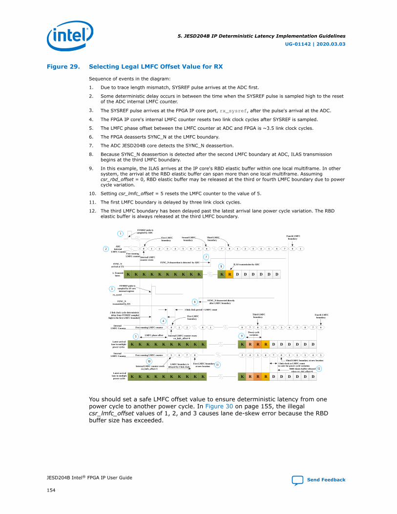
Figure 29. Selecting Legal LMFC Offset Value for RX
Sequence of events in the diagram:
1. Due to trace length mismatch, SYSREF pulse arrives at the ADC first.
2. Some deterministic delay occurs in between the time when the SYSREF pulse is sampled high to the resetof the ADC internal LMFC counter.
3. The SYSREF pulse arrives at the FPGA IP core port, rx_sysref, after the pulse's arrival at the ADC.
4. The FPGA IP core's internal LMFC counter resets two link clock cycles after SYSREF is sampled.
5. The LMFC phase offset between the LMFC counter at ADC and FPGA is ~3.5 link clock cycles.
6. The FPGA deasserts SYNC_N at the LMFC boundary.
7. The ADC JESD204B core detects the SYNC_N deassertion.
8. Because SYNC_N deassertion is detected after the second LMFC boundary at ADC, ILAS transmissionbegins at the third LMFC boundary.
9. In this example, the ILAS arrives at the IP core's RBD elastic buffer within one local multiframe. In othersystem, the arrival at the RBD elastic buffer can span more than one local multiframe. Assumingcsr_rbd_offset = 0, RBD elastic buffer may be released at the third or fourth LMFC boundary due to powercycle variation.
10. Setting csr_lmfc_offset = 5 resets the LMFC counter to the value of 5.
11. The first LMFC boundary is delayed by three link clock cycles.
12. The third LMFC boundary has been delayed past the latest arrival lane power cycle variation. The RBDelastic buffer is always released at the third LMFC boundary.
First LMFC boundary
SYSREF pulse is sampled by IP core
internal register
2 link clock cycle deterministic delay from SYSREF sampled
high to the first LMFC boundary
Free running LMFC counterInternal
LMFC Counter 0 1 2 0 1 0 1 2 3 4 5 6 7
K
SYNC_N deasserted directly after LMFC boundary
K K K K RK K K K KLatest arrival
lane in multiple power cycles
D D D D
0
Power cycle variation
Fourth LMFC boundary
1 link clock period = LMFC count
Internal LMFC counter resetscsr_lmfc_offset=0
7
Third LMFC boundary
D D
Free running LMFC counter
ADCInternal
LMFC Counter0 1 2 3 4 5 6 7 0 1 2 3 4 5 6 7 0 17
SYSREF pulse is sampled by ADC
SYNC_N transmitted by RX
0
SYNC_N deassertion is detected by ADCSYNC_N
arrival at TX
K K K K K RK K K K KL Transmit lanes D D D DK D D
ILAS transmission by ADC
Internal LMFC counter resets
First LMFC boundary
Second LMFC boundary
Third LMFC boundary
LMFC phase offset
R R
Free running LMFC counterInternal
LMFC Counter 5 6 7 0 5 6 7 0 1 2 3 4 5
RBD elastic buffer releasedwhen csr_rbd_offset=0
4
K K K K KK K K K K
Internal LMFC counter resetscsr_lmfc_offset=5
LMFC boundary is delayed by 3 link clock
First LMFC boundary at new location
R D D D D D DR R
1 link clock or LMFC countto cater for power cycle variation
6
3
K
Fourth LMFC boundary
KLatest arrival
lane in multiple power cycles
rx_sysref
1
2
3
4
5
6
7
8
9
1011
12
Third LMFC boundary at new location
You should set a safe LMFC offset value to ensure deterministic latency from onepower cycle to another power cycle. In Figure 30 on page 155, the illegalcsr_lmfc_offset values of 1, 2, and 3 causes lane de-skew error because the RBDbuffer size has exceeded.
5. JESD204B IP Deterministic Latency Implementation Guidelines
UG-01142 | 2020.03.03
JESD204B Intel® FPGA IP User Guide Send Feedback
154

Figure 30. Selecting Illegal LMFC Offset Value for RX, Causing Lane Deskew Error
First LMFC boundary
SYSREF pulse is sampled by IP core ‘s
internal register
2 link clock cycle deterministic delay from SYSREF sampled
high to the first LMFC boundary
Free running LMFC counterInternal
LMFC Counter 0 1 2 0 1 4 0 1 2 3 4 5 6 7
K
SYNC_N deasserted at LMFC boundary
K K K K RK K K K KLatest arrival
lane in multiple power cycles
D D D D
0
Power cycle variation
Fourth LMFC boundary
1 link clock period = LMFC count
Internal LMFC counter resetscsr _lmfc_offset=0
7
Third LMFC boundary
D D
SYNC_N transmitted by RX
R R
Free running LMFC counterInternal
LMFC Counter 3 4 5 6 7 0 1 3 4 5 6 7 0 1 2 3
RBD elastic buffer released
when csr _rbd_offset=0
2
K K K K KK K K K K
Internal LMFC counter resetscsr _lmfc_offset=3
LMFC boundary is delayed by 5 link clock
First LMFC boundary at new location
R D D D D D DR R
6
1
K
KLatest arrival
lane in multiple power cycles
K K K K K RK K K K KEarliest arrival lane D D DD D DK
5
D D D
RBD elastic buffer size is exceeded
rx_sysref
Third LMFC boundary at new location
RBD elastic buffer size = 8 (1)
Note:(1) RBD elastic buffer size = F x K/4; F = 1, K = 32
You can use the TX LMFC offset to align the LMFC counter in IP core to the LMFCcounter in DAC.
5. JESD204B IP Deterministic Latency Implementation Guidelines
UG-01142 | 2020.03.03
Send Feedback JESD204B Intel® FPGA IP User Guide
155

Figure 31. Example of Reducing LMFC Phase Offset between TX and RX LMFC Counter
Sequence of events in the diagram:
1. SYSREF pulse arrives at the FPGA IP core port, tx_sysref.
2. The IP core's internal LMFC counter resets after two link clock cycles.
3. SYSREF pulse is sampled by the DAC.
4. The DAC's internal LMFC counter resets after a deterministic delay.
5. The LMFC phase offset is ~3.5 link clock cycles.
6. The DAC deasserts SYNC_N at the LMFC boundary.
7. SYNC_N deassertion is detected by the JESD204B IP core.
8. Because SYNC_N deassertion is detected after the second LMFC boundary at the FPGA, ILAS transmissionbegins at the third LMFC boundary.
9. The csr_lmfc_offset is set to 4. This delays the TX LMFC boundary by 4 link clock cycles. If csr_lmfc_offsetis set to 5, the TX LMFC boundary is delayed by 3 link clock cycles.
10. The LMFC phase offset between the TX and RX LMFC reduces to 0.5 link clock cycle.
First LMFC boundary
SYSREF pulse is sampled by DAC
2 link clock cycle deterministic delay from SYSREF sampled high to the first LMFC boundary
Free running LMFC counterInternal
LMFC Counter 0 1 0 1 2 0 1 2 3 4 5
SYNC_N deasserted atthe LMFC boundary
1 link clock period = LMFC count
7
Third LMFC boundary
Free running LMFC counter
0 1 2 3 4 5 6 7 0 1 2 3 4 5 6 7 07
SYSREF pulse is sampled by FPGA
IP core
SYNC_N transmitted by DAC
0
SYNC_N deassertion is detected by the IP coreSYNC_N
arrival at TX
K K K K K RK K K K KL Transmit lanes D D D DK D D
ILAS transmission by the FPGA
Internal LMFC counter resetscsr _lmfc_offset=0
First LMFC boundary
Second LMFC boundary
Third LMFC boundary
6
Fourth LMFC boundary
Link clock
InternalLMFC Counter
Deterministic delay from SYSREF sampled high to the first LMFC boundary
LMFC phase offset
Free running LMFC counter
4 5 6 7 0 1 2 3 4 5 6 7 0 1 2 3 434InternalLMFC Counter
Internal LMFC counter resetscsr _lmfc_offset=4
First LMFC boundary at new location
K K K K K RK K K K KL Transmit lanes DK D DK K K
Reduced LMFC phase offset
K
LMFC boundary is delayed by 4 link clock
tx_sysref1
2
3
4
5
6
78
9
10
9
Second LMFC boundary
ILAS transmission by the FPGA
Alternative to tuning RBD offset at the DAC, adjusting TX LMFC offset in the FPGAhelps you to achieve deterministic latency. You should perform multiple power cyclesand read the RBD counts at the DAC to determine whether deterministic latency isachieved and RBD elastic buffer size has not exceeded.
The SYSREF pipeline registers in the FPGA introduce additional latency to SYSREFwhen detected by the IP core. Therefore, you can use TX LMFC offset to reduce oreliminate this additional latency. The next figure illustrates the technique of optimizinglatency using TX LMFC offset.
5. JESD204B IP Deterministic Latency Implementation Guidelines
UG-01142 | 2020.03.03
JESD204B Intel® FPGA IP User Guide Send Feedback
156

Figure 32. Optimizing IP Core Latency Using TX LMFC Offset
Sequence of events in the diagram:
1. The DAC samples the SYSREF pulse.
2. The DAC's internal LMFC counter resets after a deterministic delay.
3. The SYSREF pipeline registers introduces an additional 2 link clock latency.
4. The csr_lmfc_offset field is set to 4. The IP core internal LMFC counter resets after 2 link clock cycles.
5. The LMFC boundary is delayed by 4 link clock.
6. The DAC deasserts SYNC_N at the LMFC boundary.
7. SYNC_N deassertion is detected by the JESD204B IP core.
8. Because LMFC boundary is delayed by 4 link clock, the IP core detects the SYNC_N deassertion before thesecond LMFC boundary. ILAS transmission begins at the second LMFC boundary instead of the third LMFCboundary (in Figure 31 on page 156). The latency is shortened by 4 LMFC counts or link clock cycles.
1
2
3
4
5
6
7
8
First LMFC boundary
SYSREF pulse is sampled by DAC
2 link clock cycle deterministic delay from SYSREF sampled high to LMFC counter resets
Free running LMFC counterInternal
LMFC Counter 0 1 7 0 1 0 1 2 3 4 5
SYNC_N deasserted at the LMFC boundary
7
Third LMFC boundary
Free running LMFC counter 0 1 2 3 7 0 1 2 3
SYSREF pulse is sampled by FPGA
IP core
SYNC_N transmitted by DAC
0
SYNC_N deassertion is detected by IP coreSYNC_N
arrival at TX
K K K K RK K K K KL Transmit lanes D
ILAS transmission by FPGA
Internal LMFC counter resetscsr_lmfc_offset=0
First LMFC boundary
Second LMFC boundary at new location
Third LMFC boundary
6
Link clock
InternalLMFC Counter
Deterministic delay from SYSREF sampled high to the first LMFC
boundary
Free running LMFC counter 4 5 6 7 4 5 6 7InternalLMFC Counter
Internal LMFC counter resetscsr_lmfc_offset=4
First LMFC boundary at new location
K K K K RK K K K KL Transmit lanes K K
LMFC boundary is delayed by 4 link clocks
Additional 2 link clock latency caused by SYSREF pipeline registers
K K
6543
Second LMFC boundarytx_sysref
LMFC boundary is delayed by 4 link clocks
Second LMFC boundary
2 3
1
ILAS transmission by FPGA
72
7
3
D
3
4
0
K
4
0 0
Third LMFC boundary at new location
K
K
K
K
The csr_lmfc_offset field provides a convenient way to achieve deterministic latencyand potentially optimizing the IP core latency. There are other ways that you canachieve deterministic latency by using the features available at the converters. Consultthe converter manufacturer for details of these features.
5.4. Maintaining Deterministic Latency during Link Reinitialization
Link reinitialization occurs when the RX device deasserts the SYNC_N signal after linkis established.
The converters resample the SYSREF signal and reset the internal LMFC counter. Whenthe link is initially established, the IP core automatically clears thecsr_sysref_singledet bit in the syncn_sysref_ctrl register (address 0x54)
5. JESD204B IP Deterministic Latency Implementation Guidelines
UG-01142 | 2020.03.03
Send Feedback JESD204B Intel® FPGA IP User Guide
157

when it detects the SYSREF pulse. The IP core does not automatically resample theSYSREF pulse unless the jesd204_tx_avs_rst_n or jesd204_rx_avs_rst_nsignal is asserted.
If you are performing a link reset by asserting txlink_rst_n or rxlink_rst_n toreinitialize the link, set the csr_sysref_singledet bit to "1" to force the IP core toresample the SYSREF pulse without asserting the jesd204_tx_avs_rst_n orjesd204_rx_avs_rst_n signal.
5. JESD204B IP Deterministic Latency Implementation Guidelines
UG-01142 | 2020.03.03
JESD204B Intel® FPGA IP User Guide Send Feedback
158

6. JESD204B IP Debug GuidelinesThese guidelines assist you in debugging JESD204B link issues. Apart from applyinggeneral board level hardware troubleshooting technique like checking the powersupply, external clock source, physical damage on components, a fundamentalunderstanding of the JESD204B subsystem operation is important.
6.1. Clocking Scheme
To verifying the clocking scheme, follow these steps:
1. Check that the frame and link clock frequency settings are correct in the PLL IntelFPGA IP or IOPLL Intel FPGA IP.
2. Check the device clock frequency at the FPGA and converter.
3. For Subclass 1, check the SYSREF pulse frequency.
4. Check the management clock frequency. For the design examples using Arria V,Cyclone V, and Stratix V devices, this frequency is 100 MHz.
6.2. JESD204B Parameters
The parameters in both the FPGA and ADC should be set to the same values. Forexample, when you set K = 32 on the FPGA, set the converter's K value to 32 as well.Scrambling does not affect the link initialization in the CGS and ILAS phases but in theuser data phase. When scrambling is enabled on the ADC, the FPGA descramblingoption has to be turned on using the "Enable scramble (SCR)" option in the JESD204BIP core Platform Designer parameter editor. When scrambling is enabled on the FPGA,the DAC descrambling has to be turned on too.
Check these items:
• Turn off the scrambler and descrambler options as needed.
• Use single lane configuration and K = 32 value to isolate multiple lane alignmentissue.
• Use Subclass 0 mode to isolate SYSREF related issues like setup or hold time andfrequency of SYSREF pulse.
6.3. SPI Programming
The SPI interface configures the converter. Hence, it is important to check the SPIprogramming sequence and register bit settings for the converter. If you use the MIFto store the SPI register settings of the converter, mistakes may occur when modifyingthe MIF, for example, setting a certain bit to "1" instead of "0", missing or extra bits ina MIF content row.
UG-01142 | 2020.03.03
Send Feedback
Intel Corporation. All rights reserved. Agilex, Altera, Arria, Cyclone, Enpirion, Intel, the Intel logo, MAX, Nios,Quartus and Stratix words and logos are trademarks of Intel Corporation or its subsidiaries in the U.S. and/orother countries. Intel warrants performance of its FPGA and semiconductor products to current specifications inaccordance with Intel's standard warranty, but reserves the right to make changes to any products and servicesat any time without notice. Intel assumes no responsibility or liability arising out of the application or use of anyinformation, product, or service described herein except as expressly agreed to in writing by Intel. Intelcustomers are advised to obtain the latest version of device specifications before relying on any publishedinformation and before placing orders for products or services.*Other names and brands may be claimed as the property of others.
ISO9001:2015Registered

Check these items:
• For example, in the ADI AD9250 converter, Intel recommends that you firstperform register bit setting for the scramble (SCR) or lane (L) register at address0x6E before setting the quick configuration register at address 0x5E.
• Determine that each row of the MIF has the same number of bits as the datawidth of the ROM that stores the MIF.
6.4. Converter and FPGA Operating Conditions
The transceiver channels at the converter and FPGA are bounded by minimum andmaximum data rate requirements. Always check the most updated device data sheetfor this info. For example, the Arria V GT device has a minimum data rate of 611Mbps.
Ensure that the sampling rate of the converter is within the minimum and maximumrequirements. For example, the ADC AD9250 has a minimum sampling rate of 40Msps. For L = 2, M = 1 configuration, the minimum data rate of this ADC is calculatedthis way:
The minimum data rate for the JESD204B link is effectively 611 Mbps.
Check these items:
• Reduce the data rate or sampling clock frequency if your targeted operatingrequirement does not work.
• Verify the minimum and maximum data rate requirements in the devicemanufacturer's data sheet.
6.5. Signal Polarity and FPGA Pin Assignment
Verify that the transceiver channel pin assignments—SYNC_N and SYSREF (forSubclass 1 only)—device clock, and SPI interface are correct. Also verify the signalpolarity of the differential pairs like SYNC_N and transceiver channels are correct.
Check these items:
• Review the schematic and board layout file to determine the polarity of thephysical pin connection.
• Use assignment editor and pin planner to check the pin assignment and I/Ostandard for each pin.
• Use RTL viewer in the Intel Quartus Prime software to verify that the top level portare connected to the lower level module that you instantiate.
6. JESD204B IP Debug Guidelines
UG-01142 | 2020.03.03
JESD204B Intel® FPGA IP User Guide Send Feedback
160
6.6. Creating a Signal Tap Debug File to Match Your DesignHierarchy
The Signal Tap and system console are very useful tools in debugging the JESD204Blink related issues. The Signal Tap provides a dynamic view of signals.
For Intel Arria 10, Intel Cyclone 10 GX, and Intel Stratix 10 devices, the Intel QuartusPrime software generates two files, build_stp.tcl and <ip_core_name>.xml. Youcan use these files to generate a Signal Tap file with probe points matching yourdesign hierarchy.
The Intel Quartus Prime software stores these files in the <debug stp directory>. The<debug stp directory> is defined based on JESD204B wrapper and data path.
Table 90. File Directory
JESD204B Wrapper Data Path Debug stp directory
Both Base and PHY Transmitter/Duplex
<ip_variant_name>/altera_jesd204_tx_mlpcs_<Quartus_version>/synth/debug/stp
Receiver <ip_variant_name>/altera_jesd204_rx_mlpcs_<Quartus_version>/synth/debug/stp
Base only Transmitter <ip_variant_name>/altera_jesd204_tx_<Quartus_version>/synth/debug/stp
Receiver <ip_variant_name>/altera_jesd204_rx_<Quartus_version>/synth/debug/stp
Synthesize your design by running Analysis and Synthesis in the Intel Quartus Primesoftware.
1. Run analysis and synthesis.
2. Then open the Tcl console by clicking View ➤ Utility Windows ➤ Tcl Console.
3. Navigate to the <debug stp directory> as shown in Table 90 on page 161.
4. Type the following command in the Tcl console:
source build_stp.tcl
5. To generate the STP file, type the following command:
main -stp_file <stp file name>.stp -xml_file <xml_file name>.xml -mode build
The <stp file name>.stp file is generated in the <debug stp directory>.
6. The software generation script may not assign the Signal Tap acquisition clock inthe <stp file name>.stp file. Consequently, the Intel Quartus Prime softwareautomatically creates a clock pin (auto_stp_external_clock) for eachinstance. To assign an acquisition clock for the generated STP file, Intelrecommends that you perform the following assignments:
JESD204B Duplex & Simplex (Both Base & PHY) or (PHY only) IP core:-
6. JESD204B IP Debug Guidelines
UG-01142 | 2020.03.03
Send Feedback JESD204B Intel® FPGA IP User Guide
161

• For rx_link instance, assign the rxlink_clk signal.
• For tx_link instance, assign the txlink_clk signal.
• For all supported devices, except Intel Stratix 10 E-tile devices:
For rx_phy and tx_phy instances, assign the input clock of the transceiverreset controller.
• For Intel Stratix 10 E-tile devices:
For rx_phy and tx_phy instances, assign rxphy_clk[0] and txphy_clk[0]as the acquisition clock. Then, add the following set_false_path constraintin the SDC script.
set_false_path -from
<instance_name>|inst_phy|inst_xcvr|*counter_*x_ready|r_reset -to
auto_fab*sld_signaltap_inst*
Note: The PHY signals are different for Intel Stratix 10 E-tile devices. Remove theirrelevant signals and add the Intel Stratix 10 E-tile device PHY signals intothe Signal Tap Logic Analyzer.
JESD204B Simplex (Base only) IP core:-
• For rx_link instance, assign the rxlink_clk signal.
• For tx_link instance, assign the txlink_clk signal.
Note: The GUI parameter editor allows you to choose the appropriate instance foreach IP core name if your design contains more than one JESD204Binstances. For simplex core, you need to choose the RX instance followed byTX instance to generate the proper STP file.
7. Click Save to save the modified STP. A dialog box pops up with a message "Doyou want to enable Signal Tap File "<stp file name>" for thecurrent project?". Click Yes. Then, compile your design.
8. To program the FPGA, click Tools ➤ Programmer.
9. Open the generated STP file again if it has closed after step 6.
10. To observe the state of your IP core, click Run Analysis in the Signal Tap LogicAnalyzer.
You may see signals or Signal Tap instances that are red, indicating they are notavailable in your design. In most cases, you can safely ignore these signals andinstances because the software generates wider buses and certain instances thatyour design does not include.
6.7. Debugging JESD204B Link Using System Console
The system console provides access to the JESD204B IP register sets through theAvalon-MM interfaces.
To use the system console, your design must contain a Platform Designer subsystemwith the JTAG-to-Avalon-MM Master bridge or Nios II Processor component. Connectthe JESD204B IP Avalon-MM interface to the Avalon-MM master through the PlatformDesigner interconnect directly if the IP resides in the Platform Designer subsystem.Otherwise, connect the Avalon-MM interface through the Merlin slave translator if theIP is not part of the Platform Designer subsystem.
6. JESD204B IP Debug Guidelines
UG-01142 | 2020.03.03
JESD204B Intel® FPGA IP User Guide Send Feedback
162

PHY Layer for All Devices Except Intel Stratix 10 E-tile Devices
Verify the PHY status through these signals in the <ip_variant_name>.v:
Table 91. PHY Status Signals for All Supported Devices Except Intel Stratix 10 E-tileDevices
Design Signals
RX • rx_is_lockedtodata• rx_analogreset• rx_digitalreset• rx_cal_busy
TX • pll_locked• pll_powerdown• tx_analogreset• tx_digitalreset• tx_cal_busy
RX and TX (Duplex) • rx_is_lockedtodata• rx_analogreset• rx_digitalreset• rx_cal_busy• rx_seriallpbken• pll_locked• pll_powerdown• tx_analogreset• tx_digitalreset• tx_cal_busy
Use the rxphy_clk[0] or txphy_clk[0] signal as sampling clock for the Signal TapLogic Analyzer.
For a normal operation of the JESD204B RX path, the rx_is_lockedtodata bit foreach lane should be "1" while the rx_cal_busy, rx_analogreset, andrx_digitalreset bit for each lane should be "0".
For a normal operation of the JESD204B TX path, the pll_locked bit for each laneshould be "1" while the tx_cal_busy, pll_powerdown, tx_analogreset, andtx_digitalreset bit for each lane should be "0".
Measure the rxphy_clk or txphy_clk frequency by connecting the clock to theCLKOUT pin on the FPGA. The frequency should be the same as link clock frequencyfor PCS option in Hard PCS or Soft PCS mode. The frequency is half of the link clockfrequency for PCS option in PMA Direct mode.
6. JESD204B IP Debug Guidelines
UG-01142 | 2020.03.03
Send Feedback JESD204B Intel® FPGA IP User Guide
163

PHY Layer for Intel Stratix 10 E-tile Devices
Verify the PHY status through these signals in the <ip_variant_name>.v:
Table 92. PHY Status Signals for Intel Stratix 10 E-tile Devices
Design Signals
RX • rx_is_lockedtodata• phy_rx_ready• phy_rx_pma_ready
TX • phy_tx_ready• phy_tx_pma_ready
Use the rxphy_clk[0] or txphy_clk[0] signal as the acquisition clock. Then addthe following set_false_path constraint in the SDC script.
set_false_path -from
<instance_name>|inst_phy|inst_xcvr|*counter_*x_ready|r_reset -to
auto_fab*sld_signaltap_inst*
For a normal operation of the JESD204B RX path, the phy_rx_pma_ready,phy_rx_ready and the rx_islockedtodata bits for each lane should be "1".
For a normal operation of the JESD204B TX path, the phy_tx_pma_ready andphy_tx_ready bits for each lane should be "1".
Measure the rxphy_clk or txphy_clk frequency by connecting the clock to theCLKOUT pin on the FPGA. The frequency should be the same as link clock frequency.
Link Layer
Verify the RX and TX PHY-link layer interface operation through these signals in the<ip_variant_name>_inst_phy.v:
Table 93. RX and TX PHY-Link Layer Signals
Design Signals
RX • jesd204_rx_pcs_data• jesd204_rx_pcs_data_valid• jesd204_rx_pcs_kchar_data• jesd204_rx_pcs_errdetect• jesd204_rx_pcs_disperr
TX • jesd204_tx_pcs_data• jesd204_tx_pcs_kchar_data
6. JESD204B IP Debug Guidelines
UG-01142 | 2020.03.03
JESD204B Intel® FPGA IP User Guide Send Feedback
164

Verify the link layer operation through these signals in the <ip_variant_name>.v:
Table 94. RX and TX Link Layer Signals
Design Signals
RX • jesd204_rx_avs_rst_n• rxlink_rst_n_reset_n• rx_sysref (for Subclass 1 only)• rx_dev_sync_n• jesd204_rx_int• alldev_lane_aligned• dev_lane_aligned• rx_somfUse the rxlink_clk signal as the sampling clock.
TX • jesd204_tx_avs_rst_n• txlink_rst_n_reset_n• tx_sysref (for Subclass 1 only)• sync_n• tx_dev_sync_n• mdev_sync_n• jesd204_tx_int
Intel recommends that you verify the JESD204B functionality by accessing the DACSPI registers or any debug feature provided by the DAC manufacturer.
6. JESD204B IP Debug Guidelines
UG-01142 | 2020.03.03
Send Feedback JESD204B Intel® FPGA IP User Guide
165

Figure 33. JESD204B Link InitializationThis is a Signal Tap image during the JESD204B link initialization. The JESD204B link has two transceiverchannels (L = 2).
f
b
a
j
k
e
c
d
d
g h i
c
f
start of 1st ILAS multi-frame
Description of the timing diagram:
• a. The JESD204B link is out of reset.
• b. The RX CDR is locked and PCS outputs valid characters to link layer.
• c. No running disparity error and 8B/10B block within PCS successfully decodesthe incoming characters.
• d. The ADC transmits /K/ character or BC hexadecimal number to the FPGA, whichstarts the CGS phase.
• e. Upon receiving 4 consecutive /K/ characters, the link layer deasserts therx_dev_sync_n signal.
• f. The JESD204B link transition from CGS to ILAS phase when ADC transmit /R/ or1C hexadecimal after /K/ character.
• g. Start of 2nd multiframe in ILAS phase. 2nd multiframe contains the JESD204Blink configuration data.
• h. Start of 3rd multiframe.
• i. Start of 4th multiframe.
• j. Device lanes alignment is achieved. In this example, there is only one device,the dev_lane_aligned connects to alldev_lane_aligned and both signalsare asserted together.
• k. Start of user data phase where user data is streamed through the JESD204Blink.
6. JESD204B IP Debug Guidelines
UG-01142 | 2020.03.03
JESD204B Intel® FPGA IP User Guide Send Feedback
166

Transport Layer
Verify the RX transport layer operation using these signals in thealtera_jesd204_transport_rx_top.sv:
• jesd204_rx_dataout
• jesd204_rx_data_valid
• jesd204_rx_data_ready
• jesd204_rx_link_data_ready
• jesd204_rx_link_error
• rxframe_rst_n
Use the rxframe_clk signal as the sampling clock.
For normal operation, the jesd204_rx_data_valid, jesd204_rx_data_ready,and jesd204_rx_link_data_ready signals should be asserted while thejesd204_rx_link_error should be deasserted. You can view the ramp or sinewave test pattern on the jesd204_rx_dataout bus.
Figure 34. Ramp Pattern on the jesd204_rx_dataout BusThis is a Signal Tap II image during the JESD204B user data phase with ramp pattern transmitted from theADC.
Verify the TX transport layer operation using these signals in thealtera_jesd204_transport_tx_top.sv:
• txframe_rst_n
• jesd204_tx_datain
• jesd204_tx_data_valid
• jesd204_tx_data_ready
• jesd204_tx_link_early_ready
• jesd204_tx_link_data_valid
• jesd204_tx_link_error
Use the txframe_clk signal as the sampling clock.
For normal operation, the jesd204_tx_data_valid, jesd204_tx_data_ready,jesd204_tx_link_early_ready, and jesd204_tx_link_data_valid signalsshould be asserted while the jesd204_tx_link_error should be deasserted. You
6. JESD204B IP Debug Guidelines
UG-01142 | 2020.03.03
Send Feedback JESD204B Intel® FPGA IP User Guide
167

can verify the user data arrangement (shown in the data mapping tables in the TXPath Data Remapping section in the Design Examples for JESD204B IP Core UserGuide) by referring to the jesd204_tx_datain bus.
Related Information
• V-Series Transceiver PHY User Guide
• Intel Arria 10 Transceiver PHY User Guide
• Intel Cyclone 10 GX Transceiver PHY User Guide
• Intel Stratix 10 L- and H-tile Transceiver PHY User Guide
• E-tile Transceiver PHY User Guide
• AN 696: Using the JESD204B MegaCore Function in Arria V DevicesMore information about the performance and interoperability of the JESD204BIP core.
• AN 729: Implementing JESD204B IP Core System Reference Design with Nios IIProcessor As Control Unit
An example of implementing a full-featured software control flow with varioususer commands in a JESD204B system that incorporates a Nios II processor
• JESD204B Reference DesignAvailable design examples in Intel FPGA Design Store.
• Design Examples for JESD204B IP Core User GuideMore information about the TX path data remapping in the Transport Layer.
• JESD204B Intel Arria 10 FPGA IP Design Example User Guide
• JESD204B Intel Stratix 10 FPGA IP Design Example User Guide
• JESD204B Intel Cyclone 10 FPGA IP Design Example User Guide
6. JESD204B IP Debug Guidelines
UG-01142 | 2020.03.03
JESD204B Intel® FPGA IP User Guide Send Feedback
168

7. JESD204B Intel FPGA IP User Guide ArchivesIP versions are the same as the Intel Quartus Prime Design Suite software versions upto 19.1. From Intel Quartus Prime Design Suite software version 19.2 or later, IP coreshave a new IP versioning scheme.If an IP core version is not listed, the user guide for the previous IP core version applies.
IP Core Version User Guide
19.1 JESD204B Intel FPGA IP User Guide
18.1 JESD204B Intel FPGA IP User Guide
18.0 JESD204B Intel FPGA IP User Guide
17.1 JESD204B IP Core User Guide
17.0 JESD204B IP Core User Guide
16.1 JESD204B IP Core User Guide
16.0 JESD204B IP Core User Guide
UG-01142 | 2020.03.03
Send Feedback
Intel Corporation. All rights reserved. Agilex, Altera, Arria, Cyclone, Enpirion, Intel, the Intel logo, MAX, Nios,Quartus and Stratix words and logos are trademarks of Intel Corporation or its subsidiaries in the U.S. and/orother countries. Intel warrants performance of its FPGA and semiconductor products to current specifications inaccordance with Intel's standard warranty, but reserves the right to make changes to any products and servicesat any time without notice. Intel assumes no responsibility or liability arising out of the application or use of anyinformation, product, or service described herein except as expressly agreed to in writing by Intel. Intelcustomers are advised to obtain the latest version of device specifications before relying on any publishedinformation and before placing orders for products or services.*Other names and brands may be claimed as the property of others.
ISO9001:2015Registered

8. Document Revision History for the JESD204B IntelFPGA IP User Guide
Document Version Intel QuartusPrime Version
IP Version Changes
2020.03.03 19.4 19.2.0 Edited the Enable Bit reversal and Byte reversalparameter description in the JESD204B Intel FPGA IPParameters section.
2019.12.16 19.4 19.2.0 • Updated the supported maximum data rate to 19.2Gbps (for Intel Agilex devices) in the JESD204B IPQuick Reference, About the JESD204B Intel FPGAIP, and Performance and Resource Utilizationsections.
• Updated the maximum data rate value option to19.2 Gbps for Intel Agilex devices for the DataRate parameter and edited the Enable Bitreversal and Byte reversal parameter descriptionin the JESD204B Intel FPGA IP Parameters section.
2019.10.07 19.3 19.2.0 • Added advance support for Intel Agilex devices.• Updated the supported maximum data rate to 17.4
Gbps (for Intel Agilex devices) in the JESD204B IPQuick Reference and About the JESD204B IntelFPGA IP sections.
• Updated the JESD204B Intel FPGA IP Performancetable in the Performance and Resource Utilizationsection with Intel Agilex devices information.
• Updated the maximum data rate value option to17.4 Gbps for Intel Agilex devices in the JESD204BIntel FPGA IP Parameters section.
• Added a reference link to the JESD204B Intel AgilexFPGA IP Design Example User Guide.
2019.05.27 19.1 – Corrected typos in the Transmitter Registers andReceiver Registers sections; changed LEMC to LMFC.
2019.04.01 19.1 – • Added support for Intel Stratix 10 E-tile devices.• Revised the resource utilization data for version
19.1 in the Performance and Resource Utilizationsection.
• Updated the JESD204B Intel FPGA IP Performancetable with Intel Stratix 10 E-tile device informationin the Performance and Resource Utilization section.
• Updated the Channel Bonding section to includeinformation about Intel Stratix 10 E-tile devices. ForIntel Stratix 10 E-tile devices, you must usecontiguous channels to enable channel bonding withNRZ PMA transceiver channels.
• Added the Transceiver Tile option which isavailable when you target an Intel Stratix 10 devicethat supports both and H-tile and E-tile.
continued...
UG-01142 | 2020.03.03
Send Feedback
Intel Corporation. All rights reserved. Agilex, Altera, Arria, Cyclone, Enpirion, Intel, the Intel logo, MAX, Nios,Quartus and Stratix words and logos are trademarks of Intel Corporation or its subsidiaries in the U.S. and/orother countries. Intel warrants performance of its FPGA and semiconductor products to current specifications inaccordance with Intel's standard warranty, but reserves the right to make changes to any products and servicesat any time without notice. Intel assumes no responsibility or liability arising out of the application or use of anyinformation, product, or service described herein except as expressly agreed to in writing by Intel. Intelcustomers are advised to obtain the latest version of device specifications before relying on any publishedinformation and before placing orders for products or services.*Other names and brands may be claimed as the property of others.
ISO9001:2015Registered

Document Version Intel QuartusPrime Version
IP Version Changes
• Renamed the Enable Altera Debug MasterEndpoint parameter to Enable Native PHYDebug Master Endpoint as per Intel rebranding inthe Intel Quartus Prime Pro Edition software. TheIntel Quartus Prime Standard Edition software stilluses Enable Altera Debug Master Endpoint.
• Added a note to refer to the PMA Adaptation sectionin the Intel Stratix 10 E-tile Transceiver PHY UserGuide for more information about PMA Adaptationparameters.
• Edited the Transmitter Signals and Receiver Signalssections to add a note that certain signals are notapplicable for Intel Stratix 10 E-tile devices orapplicable only for Intel Stratix 10 L-tile and H-tiledevices.
• Added the following signals that are applicable onlyfor Intel Stratix 10 E-tile devices in the TransmitterSignals and Receiver Signals sections:— phy_tx_ready— phy_rx_ready— phy_tx_pma_ready— phy_rx_pma_ready— phy_tx_rst_n— phy_rx_rst_n— tx_serial_data_n— rx_serial_data_n
• Added a note in the Pin Assignments section to usethe E-Tile Channel Placement Tool to get a validpinout for Intel Stratix 10 E-tile devices.
• Added a note in the Adding External TransceiverPLLs section that Intel Stratix 10 E-tile devicedesigns do not require external PLLs.
• Added a note in the Simulating the IP CoreTestbench section that Intel Stratix 10 E-tiledevices do not support the Riviera-PRO simulator.
• Add information about Intel Stratix 10 E-tile devicesin the Testbench Simulation Flow section.
• Edited the Creating a Debug File to Match YourDesign Hierarchy section to add information aboutIntel Stratix 10 E-tile devices.
• Edited the Debugging JESD204B Link Using SystemConsole section to add information about IntelStratix 10 E-tile devices.
• Added the Transmitter Registers and ReceiverRegisters sections in the Registers chapter. Theregister information are now available in thedocument.
2018.12.10 18.1 – • Updated the Device Family Support section toindicate that the JESD204B Intel FPGA IP coresupports only Intel Stratix 10 (L-tile and H-tile)devices.
• Revised the data rate information for Intel Stratix10 devices for speed grade 2 and 3.
• Revised the resource utilization data and speedgrade information for version 18.1.
• Added resource utilization data and speed gradeinformation for Intel Stratix 10 devices whennumber of octets per frame (F) is 3.
continued...
8. Document Revision History for the JESD204B Intel FPGA IP User Guide
UG-01142 | 2020.03.03
Send Feedback JESD204B Intel® FPGA IP User Guide
171

Document Version Intel QuartusPrime Version
IP Version Changes
• Updated the Octets per frame (F) parameteroption to support F=3 in the JESD204B IP CoreParameter section. F=3 is available only for IntelStratix 10 devices.
• Categorized the following signals as debug andtesting signals in the Transmitter Signals section:— csr_tx_testmode[3:0]
— csr_tx_testpattern_a[]
— csr_tx_testpattern_b[]
— csr_tx_testpattern_c[]
— csr_tx_testpattern_d[]
• Categorized the csr_rx_testmode[3:0] signalas a debug and testing signal in the ReceiverSignals section.
• Added a note in the Receiver Signals section thatthe test pattern checker is a component in thedesign example and is not a part of the JESD204BIP core
• Added a note in the Transmitter Signals section thatthe test pattern generator is a component in thedesign example and is not a part of the JESD204BIP core
• Edited the steps for running analysis and synthesisin the Creating a Signal Tap Debug File to MatchYour Design section.
2018.05.07 18.0 – • Renamed JESD204B IP core to JESD204B IntelFPGA IP as per Intel rebranding.
• Added support for Intel Cyclone 10 GX devices.• Added simulation setup and run scripts for the
Cadence Xcelium Parallel simulator.• Added links to the JESD204B Intel FPGA IP Design
Example for Intel Cyclone 10 GX Devices UserGuide.
• Edited a typo in in the Brief Information About theJESD204B IP Core table. Changed PlatformDesigner (Standard) to Platform Designer.
• Revised the resource utilization data and speedgrade information for version 18.0.
• Updated the JESD204B IP Core Parameters andSignals sections with Intel Cyclone 10 GXinformation.
• Edited the steps in the Creating a Signal Tap DebugFile to Match Your Design Hierarchy section.
• Added a note in the Testbench Simulation Flowsection that for Intel Stratix 10 devices, resetdeassertion staggering of TX/RX analog and digitalreset happens before the assertion of TX/RX ready.
Date Version Changes
November 2017 2017.11.06 • Updated alldev_lane_aligned signal description.• Updated bonded channel requirements for Intel Stratix 10 and Intel
Arria 10 devices.• Updated instances of Qsys to Platform Designer.• Updated steps to simulate the testbench design using the Aldec Riviera-
PRO simulator.• Removed note stating that the dynamic reconfiguration is not supported
for the JESD204B IP core testbench.
continued...
8. Document Revision History for the JESD204B Intel FPGA IP User Guide
UG-01142 | 2020.03.03
JESD204B Intel® FPGA IP User Guide Send Feedback
172

Date Version Changes
• Added Base only, or Simplex TX configuration in Preset Configurationsfor JESD204B IP Core Testbench table.
• Added Provide Separate Reconfiguration Interface for Each Channelparameter in the JESD204B IP Core Parameters table.
• Updated Link Clock FMAX (MHz) for all devices in the JESD204B IP CoreFPGA Performance table.
• Added supported data rate note to Intel Arria 10 variants in JESD204BIP Core FPGA Performance table.
• Updated rx_phy and tx_phy assignments in Creating a Signal Tap DebugFile to Match Your Design Hierarchy.
• Updated the data rate support for Intel Stratix 10 devices:— For speed grade 1 to up to 16.0 Gbps.— For speed grade 2 to up to 13.5 Gbps.— For speed grade 3 to up to 12.5 Gbps.
• Updated and added example timing diagrams in Subclass 2 OperatingMode subsection.
• Updated transceiver interface signals for transmitter and receiversignals.
May 2017 2017.05.08 • Updated description for PLL/CDR Reference Clock Frequency inJESD204B IP Core Parameters.
• Added somf[] for transmitter signal.• Updated Run-Time Configuration to include statement on JESD204B IP
core parameterization for Intel Stratix 10 devices.• Added note to Registers to indicate that disabled run-time access for
registers in Intel Stratix 10 devices.• Updated data path preset value to simplex TX and simplex RX in Preset
Configurations for JESD204B IP Core Testbench table.• Clarified the device family support for Stratix 10 devices.• Added Transmitter and Receiver signal diagrams.• Added Share Reconfiguration Interface parameter in JESD204B IP
Core Parameters table.• Added note and description to Share Reconfiguration Interface in
JESD204B IP Core Parameters.• Added links to Stratix 10 device Datasheet, Stratix 10 L-Tile Transceiver
PHY User Guide, and Stratix 10 H-Tile Transceiver PHY User Guide.• Added tx_analogreset_stat, rx_analogreset_stat,
tx_digitalreset_stat, and rx_digitalreset_stat signals anddescriptions.
• Updated ADC-FPGA Subsystem Reset Scheme and FPGA-DACSubsystem Reset Scheme.
October 2016 2016.10.31 • Updated Example 2 in Clock Correlation.• Updated steps in FPGA–DAC Subsystem Reset Sequence.• Updated figure and title for JESD204B Subsystem with Shared
Transceiver Reference Clock and Core Clock and JESD204B Subsystemwith Separate Transceiver Reference Clock and Core Clock.
• Updated Subclass 1 Deterministic Latency and Support forProgrammable Release Opportunity figure.
• Updated Channel Bonding description.
May 2016 2016.05.02 • Updated the IP Core release information.• Updated the data rate support—uncharacterized support for data rates
of up to 15 Gbps.• Updated the data rate for Intel Arria 10 and Arria V GT/ST in the
JESD204B IP Core FPGA Performance table.• Updated the JESD204B IP Core FPGA Resource Utilization table.• Updated the PLL/CDR Reference Clock Frequency parameter
description.
continued...
8. Document Revision History for the JESD204B Intel FPGA IP User Guide
UG-01142 | 2020.03.03
Send Feedback JESD204B Intel® FPGA IP User Guide
173

Date Version Changes
• Updated the preset values for PLL/CDR Reference Clock Frequency,Link Clock, and AVS Clock in Table 3-8: Preset Configurations forJESD204B IP Core Testbench.
• Updated Figure 4-8 to illustrate shared clocking and renamed the title to"JESD204B Subsystem with Shared Transceiver Reference Clock andCore Clock".
• Added a new figure to illustrate separate clocking—Figure 4-9:JESD204B Subsystem with Separate Transceiver Reference Clock andCore Clock.
• Added new sections:— ADC–FPGA Subsystem Reset Sequence on page 72— FPGA–DAC Subsystem Reset Sequence on page 74— Creating a Signal Tap Debug File to Match Your Design Hierarchy on
page 161• Updated the TX path CONTROL_BUS_ WIDTH parameter description.• Revised the clock domain for jesd204_tx_data_ready signal to
txframe_clk.• Updated the description for the following registers in the register map:
— rx_regmap:• csr_frame_data_ready_err
• csr_pcfifo_full_err
• csr_pcfifo_empty_err
— tx_regmap:• csr_pcfifo_full_err
• csr_pcfifo_empty_err
• Added links to archived document in JESD204B Intel FPGA IP User GuideArchives on page 169.
November 2015 2015.11.02 • Added data rate support of up to 13.5 Gbps for Intel Arria 10 and 7.5Gbps for Arria V GT/ST devices.
• Updated the IP core FPGA performance and resource utilization values.• Added a new table to define the clock network selection for bonded
mode in channel bonding.• Added a new selection for PCS Option parameter—Enabled PMA Direct.• Updated the preset value for link clock in JESD204B IP Testbench on
page 41.• Updated the formula and description for TX/RX PHY clock.• Updated the device clock section to recommend user to supply the
device clock with the same frequency as the link clock.• Updated the description of txlink_clk, txphy_clk[], and
rxphy_clk[] signals.• Changed the default value for RX Phase Compensation FIFO empty error
enable (csr_pcfifo_empty_err_en) CSR to 0. Refer to the RXregister map for details.
• Added a new section—Design Example with Nios II Processor ControlUnit.
• Added a new topic – Maintaining Deterministic Latency during LinkReinitialization on page 157.
• Changed instances of Quartus II to Quartus Prime.
May 2015 2015.05.04 • Added support for Cyclone V FPGA device family.• Updated the JESD204B IP Core Configuration values:
— M value from 1-32 to 1-256— N' value from 4-32 to 1-32
• Updated the JESD204B IP Core FPGA Performance table.• Updated the JESD204B IP Core FPGA Resource Utilization table.
continued...
8. Document Revision History for the JESD204B Intel FPGA IP User Guide
UG-01142 | 2020.03.03
JESD204B Intel® FPGA IP User Guide Send Feedback
174

Date Version Changes
• Added new parameters to the JESD204B IP Core Parameters table:— Enable Capability Registers— Set user-defined IP identifier— Enable Control and Status Registers— Enable Prbs Soft Accumulators— Enable manual F configuration
• Added new topics:— Timing Constraints For Input Clocks on page 33— JESD204B IP Deterministic Latency Implementation Guidelines on
page 149• Revised the note in "Simulating the IP Core Testbench" to state that
VHDL is not supported in Aldec Riviera (for Intel Arria 10 devices only).• Updated the Control Unit Process Flow diagram.
December 2014 2014.12.15 • Updated the JESD204B IP Core FPGA Performance table with the datarate range.
• Updated the JESD204B IP Core FPGA Resource Utilization table.• Updated the JESD204B IP Core Parameters table with the following
changes:— Revised the parameter name of Enable PLL/CDR Dynamic
Reconfiguration to Enable Transceiver DynamicReconfiguration.
— Added information for a new parameter—Enable Altera DebugMaster Endpoint.
— Added details about the rule check for parameter N' value.• Added a new topic—Integrating the JESD204B IP in Platform Designer
on page 31.• Updated Overview of the JESD204B IP Core Block Diagram, Transmitter
Data Path Block Diagram, and Receiver Data Path Block Diagram.• Added a new table—Register Access Type Convention—to describe the
access type for the IP core registers.• Added new signals description for jesd204_tx_controlout and
jesd204_rx_controlout.• Added CONTROL_BUS_WIDTH parameter and description for the
assembler and deassembler.• Added information on how to run the Tcl script using the Quartus II
software before compiling the design example.• Updated the section on Debugging JESD204B Link Using System
Console on page 162 with verification information for TX PHY-link layerinterface, TX link layer, and TX transport layer operations.
June 2014 2014.06.30 • Updated Figure 2-1 to show a typical system application.• Updated the list of core key features.• Updated the Performance and Resource utilization values.• Updated the Getting Started chapter to reflect the new IP Catalog and
parameter editor.
continued...
8. Document Revision History for the JESD204B Intel FPGA IP User Guide
UG-01142 | 2020.03.03
Send Feedback JESD204B Intel® FPGA IP User Guide
175

Date Version Changes
• Added the following new sections to further describe the JESD204B IPcore features:— Channel Bonding— Datapath Modes— IP Core Variation— JESD204B IP Core Testbench— JESD204B IP Core Design Considerations— TX Data Link Layer— TX PHY Layer— RX Data Link Layer— RX PHY Layer— Operation— Dynamic Reconfiguration— JESD204B IP Core Debug Guidelines
• Updated the Clocking scheme section.• Added new transceiver signals that is supported in Intel Arria 10
devices.• Updated the Transport Layer section.• Added run-time reconfiguration parameter values in the System
Parameters section.• Updated the file directory names.
November 2013 2013.11.04 Initial release.
8. Document Revision History for the JESD204B Intel FPGA IP User Guide
UG-01142 | 2020.03.03
JESD204B Intel® FPGA IP User Guide Send Feedback
176