Embed Size (px)
Citation preview

Jet Propulsion Laboratory
Microdevices Laboratory
2016–2017 | ANNUAL REPORT
National Aeronautics and Space Administration

ABOUT THE COVER: “What could be a bigger quest than setting out to understand the origin, nature, and evolution of the universe? How did it
begin? How does it work? And ultimately how will it end? To help answer these questions, JPL’s reach has extended from Earth to the Sun to the
Big Bang, as we investigate how galaxies and stars form and evolve, the nature of the interstellar medium, and the cosmic microwave background
left from the universe’s earliest epoch.” *Part of this NASA/JPL quest is to gain not only a better understanding of our solar system but to also
unlock the mysteries of planets we’ve just begun to discover revolving around other stars in our galaxy and beyond.
COVER PHOTO: A digital composition of solar system planets and important moons overlaid on a star field with the Milky Way galaxy highlight
elements of the discovery and exploration domains of NASA’s mission directorates. MDL invents and develops unique devices in conjunction with
a diverse set of state-of-the-art fabrication technologies to support NASA missions across the full breadth of these domains. MDL is continually
assessing the forefront of fundamental research and fabrication technology to create the next generation of key space devices for NASA and
our nation. A subset of activities is highlighted in this report.
*NASA/JPL Quest #6 retrieved from: https://jpl.nasa.gov/jpl2025/quests/6/
The Microdevices Laboratory (MDL) is at the forefront of the inspiration, innovation, and implementation of new technologies developed from cutting-edge research at JPL and throughout NASA.
Located in the Southern Hemisphere, NGC 3324 is at the northwest corner of the Carina Nebula (NGC 3372), home of the Keyhole Nebula and the active, outbursting star Eta Carinae. The glowing nebula has been carved out by intense ultraviolet radiation and stellar winds from several hot, young stars.

INSPIRATION INNOVATIONIMPLEMENTATION
The Jet Propulsion Laboratory’s Microdevices Laboratory has,
since 1989, been a key player in JPL’s dedicated efforts to create
and deliver high-risk, high-payoff technology for NASA’s planetary,
astrophysics, and Earth science missions. From the beginning,
MDL has cultivated an environment that values and promotes
leadership, vision, and innovation while inventing, improving, and
implementing new technologies that drive NASA’s ongoing quest
to probe the mysteries of the universe. This is accomplished via the
talent, dedication, and hard work of MDL’s scientists, researchers,
and staff, along with sustained and insightful investments in infra-
structure and equipment.
Visit us online at microdevices.jpl.nasa.gov.

... MORE THAN TWENTY MDL DEVICES AND COMPONENTS HAVE FLOWN IN SPACE, ENABLING NEW SCIENCE MEASUREMENTS AND INVESTIGATIONS FOR JPL AND NASA.
Dr. Robert GreenDIRECTORJPL MICRODEVICES LABORATORY
It is a privilege and responsibility to be selected as the third director of JPL’s Microdevices Laboratory (MDL). For more than 15 years, my research has used advanced imaging spectrometer instrumentation enabled by unique optical components invented at MDL. These instruments have been used to test hypotheses and pursue investigations on Earth, the Moon, and Mars. Currently the most advanced MDL electron-beam fabricated diffraction grating and optical slit are being incorporated in the Mapping Imaging Spectrometer for Europa
(MISE) to address key science questions related to habitability. Through this experience, as well as through my interactions with other investigators, my appreciation of MDL has come to be both broad and deep.In our 2017 overall assessment, the clear evidence of MDL’s success for JPL is revealed through the more than twenty MDL devices and components that have flown in space, enabling new science measurements and investigations for JPL and NASA. Ten more MDL devices are currently incorporated in space missions in development. In addition, a diverse set of new MDL devices are essential elements of other potential future NASA missions. A wide range of MDL devices have also been developed and tested in airborne instruments, sounding rocket investigations, and ground based systems to advance technologies for future space missions as well as achieve key technology breakthroughs for our nation.Three key elements underpin MDL’s extraordinary track record of success for JPL and NASA. First, there is an exceptional group of scientists and technologists who conceive and develop unique devices to enable new measurements and new capabilities for NASA. Second, there is a unique and diverse set of state-of-the-art micro and nano-fabrication tools located in one place to allow the development of original devices. The third element is the optimized facility and infrastructure that supports these tools and allows them to be used in novel ways and combinations to invent new devices and with the rigor required for use in space missions. These elements have enabled the spectacular results highlighted in the subsequent pages of this report that in fact represent only a subset of all the advances being made at MDL. This report also highlights some of the high-risk, high-payoff technology concepts under development, which highlight MDL’s forward looking philosophy in research and development. Over the next year, we will work to strengthen and advance MDL in each of these areas, insuring that MDL will continue to deliver breakthrough devices, components, and technologies for NASA and our nation through the 2025 and 2035 time frames.
MDL DIRECTOR’S LETTER

WE ARE DETERMINED TO CONTINUE TO DO
GREAT RESEARCH, DEVELOP
BREAKTHROUGH TECHNOLOGIES
AND DEVICES, AND CONTINUE TO
REMAIN CRITICAL FOR NASA/JPL
FUTURE MISSIONS.
Dr. Siamak Forouhar DEPUTY DIRECTOR
JPL MICRODEVICES LABORATORY
At JPL’s Microdevices Laboratory we conduct valuable research and make new discoveries by developing technologies and instruments for exploring the solar system, deep space, and our own planet. I feel fortunate to have been selected as the MDL Deputy Director since the position was created in 2007 by Paul Dimotakis, former JPL Chief Scientist, and Jonas Zmuidzinas, former MDL Director. Working under Jonas’ guidance and leadership, and then later under Chris Webster, the second MDL Director, has been a significant learning process and privilege for me. Engaging with the outstanding and talented technical team at MDL has also been extremely rewarding, and I draw inspiration from rich interactions with my peers. MDL is truly a unique environment that attracts world-class personnel.From the beginning, our vision for MDL was to perform innovative and unique research and development in micro- and nano-technology, and
to infuse these technologies into projects of interest for JPL and NASA in the areas of astrophysics, planetary and Earth science, Department of Defense space and terrestrial missions, and commercial industry. As evident from our 20-year track record, MDL-developed technologies have had a significant impact on instruments for exploration of new science. In January 2017, Dr. Robert Green, a JPL senior research scientist and JPL Fellow, was appointed as the third Director of MDL. I was asked to continue in my key role as the MDL Deputy Director, bridging this exciting transition and continuing forward.
We are determined to continue to do great research and develop breakthrough technologies and devices, and have every expectation that MDL will continue to play a critical role in NASA/JPL missions.
MDL DEPUTY DIRECTOR’S STATEMENT

VISION THE PATHWAY TO
ACHIEVE OUR QUESTS
QUESTSTHE PROFOUND
QUESTIONS WE STRIVE TO ANSWER
CULTUREOUR VALUES, BELIEFS, AND CHARACTER THAT MAKE THE LAB UNIQUE
THRUSTSINITIATIVES DESIGNED
TO SUPPORT OUR CULTURE AND QUESTS
We serve the nation by exploring space in pursuit of discoveries that benefit humanity
1. What changes are happening to our own planet?2. How can we help pave the way
for human exploration of space?3. How did our solar system form and evolve?4. Has there ever been life elsewhere in our solar system?
Could it be there today?5. Are there planets like Earth elsewhere in the universe?6. How did the universe begin, and how is it evolving?7. Can we use our unique expertise to serve our nation
and its people?
Organizations are unique in different ways, and JPL has particular reasons for seeing its identity as one-of-a-kind
1. Creating the workplace of the future
2. Innovating what we do and how we do it
3. Inspiring the world through our stories
OUR ROLE IN SPACE EXPLORATION ON BEHALF OF NASA AND THE NATION
JPL

JPL BEYOND
An artist’s illustration of the seven TRAPPIST-1 planets, in their respective orbits.

With atomic-level e-beam etching, optical surfaces can now be manufactured with incredible accuracy at MDL, unleashing new and powerful possibilities as we examine the planets in our solar system as well as other worlds orbiting distant stars.
New research with carbon nanotubes is creating sticky “foodpads” that can successfully adhere to a variety of dusty, uneven surfaces and clean themselves for re-use. Further development promises better mobility and adhesion for tiny robots in extreme environments.
The tunable laser spectrometer, built with solid-state lasers from MDL, continues to generate great science on Mars. Semiconductor lasers will continue to revolutionize the way planetary science, and many other remote sensing applications, are pursued.
12
22
30
SCULPTING WITH ELECTRONS
STICKY LITTLE ROBOTS
LASERS ON MARS KEEP GOING
JPL
| M
ICR
OD
EVI
CE
S L
AB
OR
ATO
RY
| 20
16-2
017
AN
NU
AL
RE
PO
RT
6
SUCCESS STORIESMDL 2016-2017

New advancements in the micromachining via electronic etching promise tiny silicon-based sensor arrays, made with unprecedented accuracy and sensitivity, for future space missions.
MDL designed and fabricated instru-mentation has flown via a high-altitude balloon for three weeks in the skies above Antarctica, offering new astronomical observational opportunities via super-cooled superconducting detectors.
All space telescopes now use solid-state imaging detectors with exceptional sensitivity and resolution. Advances in superlattice doping have advanced these detectors to levels inconceivable just a few years ago.
38
44
50
SCULPTING WITH IONS
FROM ANTARCTICA TO THE STARS
PULLING LIGHT FROM THE DARKNESS
7
INSPIR
ATION
• INN
OVA
ION
• IMPLEM
ENTATIO
N
MDL is at the forefront of the innovation and implementation of new technologies to inspire and enable cutting-edge research at JPL and throughout NASA.

JPL
| M
ICR
OD
EVI
CE
S L
AB
OR
ATO
RY
| 20
16-2
017
AN
NU
AL
RE
PO
RT
8
DR. THOMAS L. KOCH, COMMITTEE CHAIR Dean of College of Optical Sciences and Professor of Optical Sciences —University of Arizona
DR. BARBARA WILSON, COMMITTEE CO-CHAIR Retired Chief Technologist —Jet Propulsion Laboratory
DR. EUSTACE DERENIAK, FORMER CHAIRMAN (2008–2015) Professor of Optical Sciences, Electrical and Computer Engineering—University of Arizona
JPLMeeting every two years to review the ongoing work at MDL and make valuable suggestions for future directions, the Visiting Committee, consisting of a broad spectrum of highly talented and accomplished individuals, has recognized the leadership, vision, and innovation of MDL. They have acknowledged that MDL is a key national asset with unique state-of-the-art capabilities and staff well focused on space applications of micro- and nanotechnologies. The committee’s reports have been of tremendous value in the pursuit of the highest quality research and development programs targeted toward the key scientific and technical goals of interest to NASA and our other sponsors.
DR. SANJAY BANERJEE Director of Microelectronics Research Center and Professor of Electrical and Computer Engineering—University of Texas at Austin
DR. JED HARRISON Professor of Chemistry and Department Chair —University of Alberta
MR. GILBERT HERRERA Director of the Laboratory for Physical Sciences—University of Maryland, College Park, MD
DR. WILLIAM HUNT Professor of Electrical and Computer Engineering—Georgia Institute of Technology
MR. GEORGE KOMAR Associate Director—NASA’s Earth Science Technology Office (ESTO)
DR. GREGORY KOVACS Professor of Electrical Engineering and courtesy appointment to Department of Medicine, Division of Cardiovascular Medicine—Stanford University
VISITING COMMITTEEMICRODEVICES LABORATORY

9
INSPIR
ATION
• INN
OVATIO
N • IM
PLEMEN
TATION
The committee recognizes MDL as a key national asset with unique state-of-the-art capabilities and staff well focused on space applications of micro- and nanotechnologies... Much of the work presented is absolutely world-class, and the staff is enthusiastic and dedicated to advancing the state of the art in their area to make a difference for JPL and NASA. It was evident to the committee that the blend of scientific mission and technical challenges is working for JPL/MDL (and)... this team continues to develop world-leading processes and capabilities. In many cases, MDL work defines the state of the art. MDL is truly the “jewel in the crown.” —MDL Visiting Committee
DR. VENKATESH NARAYANAMURTI Director of Science, Technology and Public Policy Program and Professor of Physics —Harvard University
DR. OSKAR PAINTER Professor of Applied Physics —California Institute of Technology
ALBERT P. PISANOProfessor and Dean of the School of Engineering—UC San Diego
DR. REGINA RAGAN Professor of Chemical Engineering and Materials Science —University of California, Irvine
DR. DONALD REAGO Director of Communications, Electronic Research, Development and Engineering Center (CERDEC)—Night Vision and Electronic Sensors Directorate (NVESD)
DR. ROBERT WESTERVELT Professor of Physics and Applied Physics —Harvard University
JONAS ZMUIDZINASFormer JPL Chief Technologist, former Director of JPL’s Microdevices Laboratory, and Merle Kingsley Professor of Physics —California Institute of Technology
MR. DAVID SANDISONDirector of the Center for Microsystems Science, Technology & Components —Sandia National Laboratories
DR. MEIMEI TIDROWChief Scientist for Focal Plane Arrays at the U.S. Army RDECOM CERDEC—Night Vision and Electronic Sensors Directorate (NVESD)

12
SCULPTING WITH ELECTRONS
Heavy Water 14
OH Radical Understanding 15 Blacker Than Black 16
Superlattice- Doped Detectors 18
Less Noise More Data 20
Simply Radiant 21
STICKY LITTLE ROBOTS
A Cometary Close-Up 24 Seeing Past Sunlight 26 Smelling Fire in Space 27 A New Twist on Life 28 LASERS ON MARS KEEP GOING
High-Performance Focal Plane Arrays 32
Nanowire Detectors 34
Micro-Optics for the Martian Surface 36
Wide-Application Infrared Detectors 37
22
30
12
14
24
18
22
42 38
44
46
47
4854
55 57
49
53
56
58
50
43
16
2015
21
26
28
3234
36
37
30
27
40

TABLE OFCONTENTS
SCULPTING WITH IONS
Crafting with Angstrom-Level Precision 40 Counting Photos 42 Smaller, Better, Tougher 43
FROM ANTARCTICA TO THE STARS
Primeval Illumination 46
Electronics for Space 47
Flatter Lenses 48
Extraterrestrial Earthquakes 49
PULLING LIGHT FROM THE DARKNESS
Well-Tuned Lasers 53
UV Observations Made Small 54
Very Cool Sensors 55
Communicating with Light 56
Message in an Interstellar Bottle 57
Fabricating the Future 58
MDL EQUIPMENT, PUBLICATIONS, PATENTS, AND AWARDS
38
50
63
44

MICRODEVICES ENGINEERRICHARD MULLERRichard Muller is in charge of operating the MDL’s JEOL JBX 9500FS e-beam lithography system and associated tools. During his 29 years at JPL, he has operated three e-beam tools and has contributed to the development and delivery of many optical and electronic components for research and flight projects.
PRINCIPAL ENGINEERDR. DANIEL WILSONDaniel Wilson (PhD in Electrical Engineering, Georgia Institute of Technology) leads the development of electron-beam–fabricated diffractive optics and imaging spectrometer gratings at JPL, including many for airborne and spaceborne flight instruments. He was awarded the NASA Exceptional Technology Achievement Medal and the JPL Lew Allen Award for his work.
The MDL develops electron-beam lithography techniques to fabricate unique nanostructures and optics that enable JPL instruments to perform novel measurements and achieve unmatched performance. Our processes for direct-write grayscale e-beam lithography combine outstanding flexibility with extreme precision, allowing rapid prototyping of unique optical components. This allows instrument designers to iteratively design and test novel designs that require optics not available from commercial suppliers. Advanced e-beam–fabricated components have enabled many revolutionary airborne and spaceborne optical instruments.
SCULPTING WITH ELECTRONSINDIVIDUAL SOLUTIONS FOR REFRACTIVE AND DIFFRACTIVE MICRO OPTICAL ELEMENTS, EVEN ON NON-STANDARD OR NON-FLAT SURFACES, CAN BE REALIZED IN CLOSE COLLABORATION WITH DESIGN AND INTEGRATION.
!E-beam-fabricated blazed convex grating (12 mm diameter) for an ultraviolet Offner imaging spectrometer.
JPL
| M
ICR
OD
EVI
CE
S L
AB
OR
ATO
RY
| 20
16-2
017
AN
NU
AL
RE
PO
RT
12
SUCCESS STORYMDL 2016–2017
13
INSPIR
ATION
• INN
OVATIO
N • IM
PLEMEN
TATION
b
d
e
a
c
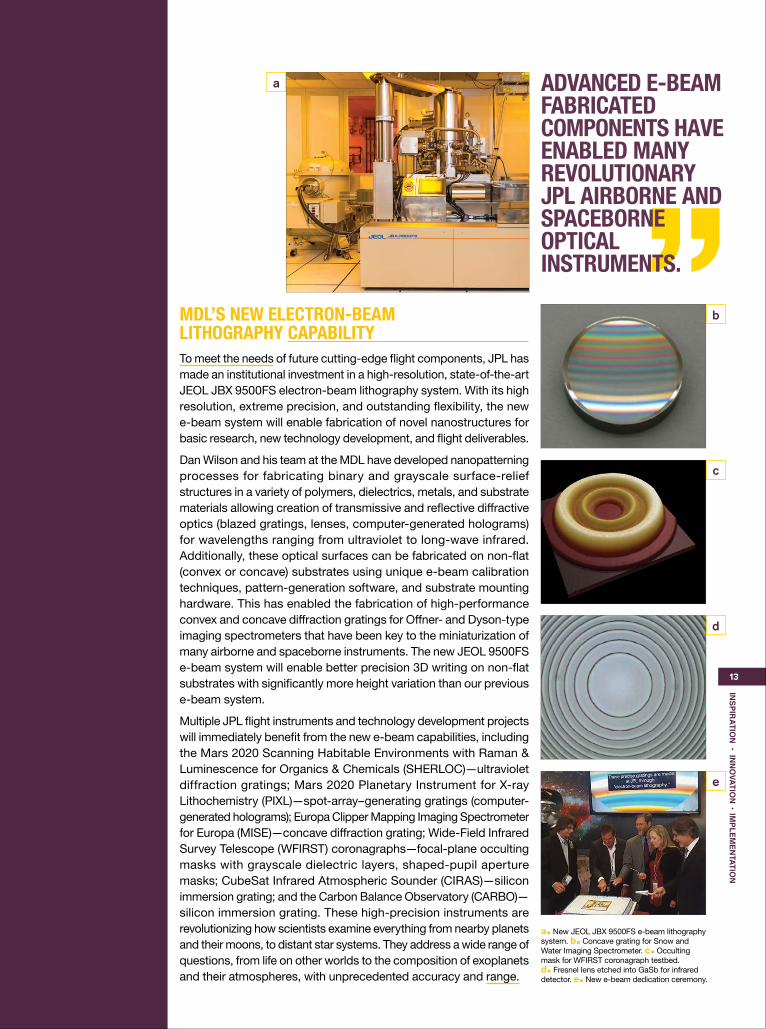
To meet the needs of future cutting-edge flight components, JPL has made an institutional investment in a high-resolution, state-of-the-art JEOL JBX 9500FS electron-beam lithography system. With its high resolution, extreme precision, and outstanding flexibility, the new e-beam system will enable fabrication of novel nanostructures for basic research, new technology development, and flight deliverables.
Dan Wilson and his team at the MDL have developed nanopatterning processes for fabricating binary and grayscale surface-relief structures in a variety of polymers, dielectrics, metals, and substrate materials allowing creation of transmissive and reflective diffractive optics (blazed gratings, lenses, computer-generated holograms) for wavelengths ranging from ultraviolet to long-wave infrared. Additionally, these optical surfaces can be fabricated on non-flat (convex or concave) substrates using unique e-beam calibration techniques, pattern-generation software, and substrate mounting hardware. This has enabled the fabrication of high-performance convex and concave diffraction gratings for Offner- and Dyson-type imaging spectrometers that have been key to the miniaturization of many airborne and spaceborne instruments. The new JEOL 9500FS e-beam system will enable better precision 3D writing on non-flat substrates with significantly more height variation than our previous e-beam system.
Multiple JPL flight instruments and technology development projects will immediately benefit from the new e-beam capabilities, including the Mars 2020 Scanning Habitable Environments with Raman & Luminescence for Organics & Chemicals (SHERLOC)—ultraviolet diffraction gratings; Mars 2020 Planetary Instrument for X-ray Lithochemistry (PIXL)—spot-array–generating gratings (computer-generated holograms); Europa Clipper Mapping Imaging Spectrometer for Europa (MISE)—concave diffraction grating; Wide-Field Infrared Survey Telescope (WFIRST) coronagraphs—focal-plane occulting masks with grayscale dielectric layers, shaped-pupil aperture masks; CubeSat Infrared Atmospheric Sounder (CIRAS)—silicon immersion grating; and the Carbon Balance Observatory (CARBO)—silicon immersion grating. These high-precision instruments are revolutionizing how scientists examine everything from nearby planets and their moons, to distant star systems. They address a wide range of questions, from life on other worlds to the composition of exoplanets and their atmospheres, with unprecedented accuracy and range.
MDL’S NEW ELECTRON-BEAM LITHOGRAPHY CAPABILITY
a§ New JEOL JBX 9500FS e-beam lithography system. b§ Concave grating for Snow and Water Imaging Spectrometer. c§ Occulting mask for WFIRST coronagraph testbed. d§ Fresnel lens etched into GaSb for infrared detector. e§ New e-beam dedication ceremony.
ADVANCED E-BEAM FABRICATED COMPONENTS HAVE ENABLED MANY REVOLUTIONARY JPL AIRBORNE AND SPACEBORNE OPTICAL INSTRUMENTS.

IN HIS WORDS
WHAT DO YOU ENJOY MOST ABOUT WORKING AT MDL?MATHIEU• I really enjoy working on projects that are at the boundaries of our technology knowledge. We are always pushing those boundaries and we are working in a great environment, with colleagues that are known worldwide for their accomplishments in their respective fields of interest. Our work is very challenging and empowering.
WHAT ELSE DO YOU THINK IS IMPORTANT TO TELL SCIENCE NEWS READERS, OR THE PUBLIC IN GENERAL?MATHIEU• To realize advancements in science and technology, incredibly hard work of several people, all working as a team, is necessary. The combination of different fields of expertise leads to novel advancements—that would not be likely working within a single discipline.
Mathieu Fradet is a member of the Advanced Optical and Electro-Mechanical Microsystems group at JPL’s Microdevices Laboratory. His expertise is in the electrical and optical characterization and packaging of GaSb-based diode lasers and interband cascade laser (ICLs), and InP-based quantum cascade lasers (QCLs).
Water is the most important trace species in Earth’s atmosphere and heavily influences the radiative balance of our planet. The isotopic composition of water vapor provides unique information about convective processes and transport in the atmosphere, and isotopes are potentially powerful diagnostics for understanding processes near the tropical tropopause, where both in situ dehydration and convective transport of water play significant roles.
The preferential deposition of heavy water (HDO) as ice is a fundamental tracer in the geosciences, used for understanding paleoclimate and water cycling in Earth’s history. During the formation of ice clouds, HDO freezes preferentially, causing the ratio of HDO/H20 to decrease in the remaining vapor. The evolution of this ratio can be used to investigate small-scale processes like crystal growth, or large-scale processes by which air moves from Earth’s surface to the upper troposphere or lower stratosphere.
The Moyer group from the University of Chicago uses absorption spectroscopy to make measurements of water vapor isotopologues. Due to the extremely dry conditions at the targeted altitude of 12–20 km, a cavity enhanced method with an effective path length of 8 km using a 90-cm cell is needed to detect the weak signals. The instrument will be flown in a research aircraft during the StratoClim campaign out of Kathmandu, Nepal, in mid-2017, during the Asian Summer Monsoon. Measuring the isotopic composition of air in and above weather patterns such as the Asian Summer Monsoon, and monitoring the origin and growth of cirrus clouds in that region, will shed light on the mechanisms and timescales of vertical transport. These are important to Earth’s energy budget, and this will be the first time such measurements have been made in situ.
A key element of this HDO instrument is a high-power, tunable, narrow-linewidth laser source at the relevant water-vapor absorption energies in the mid-IR. MDL’s semiconductor laser group has developed and delivered a unique high-power (more than 20 mW), tunable single-mode GaSb-based diode laser, and emitting light at 2.65 µm for this research program. The development of continuous-wave (CW) and high-power semiconductor lasers in the mid-infrared (mid-IR) spectral region has bridged the longstanding gap in commercially available technology.
Not all water is created equal. Some forms are heavier than others, and understanding the abundance of the heavier isotopes of water can help us understand important weather cycles on Earth. During the formation of ice clouds, the heavier isotopes of water such as HDO, or heavy water, preferentially freeze, causing the ratio of HDO/H2O to decrease in the remaining vapor.
Measuring the isotopic composition of air in and above weather patterns and cloud formation in regions of turbulent weather such as monsoons can illuminate patterns of moisture transport in the atmosphere, and enhance our understanding of weather patterns dramatically.
ENHANCED MEASUREMENTS OF WATER VAPOR ISOTOPES
HEAVY WATER
MATHIEU FRADET
a
b
a§ A semiconductor laser fabricated at MDL inside a TO-3 package. b§ The HDO instrument lives under the bubble-like fairing on top of the M55 Geophysica airplane.JP
L |
MIC
RO
DE
VIC
ES
LA
BO
RAT
OR
Y |
2016
-201
7 A
NN
UA
L R
EP
OR
T
14
WATER IS THE MOST
IMPORTANT TRACE SPECIES
IN EARTH’S ATMOSPHERE AND HEAVILY INFLUENCES
THE RADIATIVE BALANCE OF OUR PLANET.

Planetary atmospheres are complex systems that behave almost like living organisms, with seemingly random behaviors that can stymie simple observation and prediction methods. Newly developed semiconductor lasers built at the MDL will enable enhanced understanding of the effects of OH in the atmospheric chemistry of both Earth and Mars, a critical step towards learning about the broader behaviors of the gaseous envelopes surrounding both worlds.
Semiconductor lasers emitting near 2.9 µm are a critical component of compact and reliable spectroscopic sensors for the measurement of hydroxyl radicals, OH, which are crucial components of the atmospheres of Earth and Mars. For example, in Earth’s atmosphere, ozone, which is important in blocking short-wave UV from reaching the surface and is a key greenhouse gas, is controlled by reactions involving OH. New advances in compact, robust instruments have resulted from the use of mid-IR lasers that open the door to detection limits of parts per million or less, and could be deployed on small aircraft, balloons, and planetary probes.
To realize the development of such devices, the MDL semiconductor laser group teamed up with the State University of New York at Stony Brook (SUNY), a world leader in the development and epitaxial growth of diodes and type-I cascade diodes emitting in the 2 to 4 µm wavelength. This collaboration has led to the first single-frequency laterally coupled distributed feedback type-I cascade diode laser. This newly developed structure successfully bridged the gap in high-power semiconductor lasers near 3 µm. Lasers have been developed at 2.9 µm, the wavelength needed to measure a pair of fundamental rotational bands of the OH radical. To facilitate the study of the tropospheric impact of OH radials on ozone depletion and the cycle of greenhouse gases in Earth’s atmosphere, we delivered a single-frequency, high-power laser for the first OH measurements in the Infrared Kinetic Spectroscopy (IRKS) apparatus that reproduces conditions of pressure and temperature relevant to the atmospheres of Earth and Mars. The IRKS apparatus has also been used to study the rates of chemical reactions that control the abundance of OH in the atmosphere. These measurements will help researchers to understand the complex interactions of OH in the atmospheres of both planets.
TYPE-I CASCADE DIODE LASERS EMITTING NEAR 2.9 MICRONS FOR OH RADICALS ABSORPTION MEASUREMENTS
c
b
a
Optical wavelength (nm)
Sig
nal (
mV
)
2901.1
-100
-50
0
50
2901.0 2900.9 2900.8
15
INSPIR
ATION
• INN
OVATIO
N • IM
PLEMEN
TATION
Dr. Sander is a Senior Research Scientist in JPL’s Earth Science Section. His work focuses on laboratory photochemistry and kinetics of Earth and planetary atmospheres, measurements of atmospheric trace gases and greenhouse gases, and development of new instruments for studying atmospheric composition from space.
OH RADICAL UNDERSTANDING
STANLEY SANDER | MATHIEU FRADET
a§ Scanning electron microscope (SEM) image of MDL’s laterally coupled (LC) distributed feedback (DFB) laser. Lateral gratings along the ridge sidewall are written with electron-beam lithography, and the grating pitch selects the single-frequency emission wavelength. b§ Signal intensity measured at the detector as a function of the laser frequency.The dips in the signal are due to OH absorption using the MDL laser. c§ Dr. Clifford Frez and PhD graduate student Aileen Hui working on the alignment of the MDL laser into the IRKS apparatus for OH measurements.
NEWLY DEVELOPED SEMICONDUCTOR LASERS BUILT AT MDL WILL ENABLE ENHANCED UNDERSTANDING OF THE EFFECTS OF OH IN THE ATMOSPHERIC CHEMISTRY OF BOTH EARTH & MARS...

BLACKER THAN BLACK
KARL YEE | VICTOR WHITE BALA BALASUBRAMANIAN
MDL’s microfabricated black materials greatly reduce stray light in optical instruments. Candidate choices include gold black, carbon nanotubes, and black silicon. Black silicon is chosen for its robustness, lower reflectivity, and wider bandwidth. Since the proof of concept in 2008, ultraprecise optical spectrometer slits with black silicon built into them have flown on multiple instruments (e.g., HyTES, AVIRIS, UCIS, HyspIRI, MaRS2, PRISM, NEON, and SWIS), and the technology is considered standard for JPL’s imaging spectrometers.
A recent application of this material is in the masks of the WFIRST shaped-pupil coronagraph, the goal of which is to image and characterize exoplanets. The suppression of the glare from the parent star, while simultaneously imaging the orbiting planet, requires typical contrast levels of a billion to one—a problem that has been described as being analogous to imaging a firefly sitting on a searchlight from over 1000 miles away.
BLACK SILICON APPLICATIONS
a
JPL
| M
ICR
OD
EVI
CE
S L
AB
OR
ATO
RY
| 20
16-2
017
AN
NU
AL
RE
PO
RT
16
a§ A black silicon mask to suppress starlight to reveal light from an orbiting exoplanet that is up to a billion times fainter.
Victor White is a process engineer in the Nano and Micro Systems (NaMS) group at JPL’s Microdevices Laboratory (MDL). Victor specializes in using MDL’s fabrication tools to shape silicon-based materials into a host of flight-enabling structures. Most of his current work involves applications of black silicon, which is among the blackest engineered materials on the planet, into ultraprecise optical components for flight applications.
IN HIS WORDS
WHAT DO YOU ENJOY MOST ABOUT WORKING AT MDL OR JPL?KARL• We are currently living in a golden age of space exploration. Discoveries are being made daily in astronomy and astrophysics, and JPL is at the center of all of this exciting research. Why would anyone want to work anywhere else?
Dr. Yee is a senior technologist in the Nano and Micro Systems (NaMS) group, with expertise in MEMS design, fabrication, and packaging processes. His primary area of research is in resonant vibratory inertial sensors. He has been the principal investigator on several programs for NASA, DARPA, and the Army.
How do you create the darkest black substance possible? Black silicon is the answer, utilizing the surface texturing of single crystal silicon. This process creates a surface with a dense forest of dark, needle-like structures. With this modification the material becomes highly absorbing of visible and infrared radiation—it is the darkest material that can be manufactured. This new technology is being utilized by the MDL to provide the maximum reduction of stray light in optical instrumentation.
MDL’S MICRO-FABRICATED
BLACK MATERIALS
GREATLY ENHANCE THE
REDUCTION OF STRAY LIGHT
IN OPTICAL INSTRUMENTS.

b c
e
f
d
To accomplish this, shaped-pupil masks with extremely black micron-scale features in a highly reflective background were designed and developed. Black silicon, optimized for a very low specular reflectivity of just ~10–7 in the wavelength band from 0.4 to 1 micron, accomplished these goals. This instrument complements other techniques for searching for exoplanets and will also enable space-based spectroscopic analysis of light from these planets.
MDL is also using electron-beam lithography and deep reactive ion etching of thin silicon wafers to produce small, laboratory-scale starshade masks for experiments at Princeton University.
These experiments are validating the concept of flying a large starshade, tens of meters in diameter, in front of a space telescope, to block starlight and enable the detection of the faint reflected light from Earth-like planets orbiting the star. Measurements of the light-suppression effectiveness of these beautiful submicron, precision flower-like apertures support the expectations for the performance of future full-scale starshades.
17
INSPIR
ATION
• INN
OVATIO
N • IM
PLEMEN
TATION
b,c§ OCO-2 spectrometer slit.
d§ Development of black Si technology to enhance the performance of imaging spectrometers for Earth science applications.
e§ SEM image showing the typical details of a petal edge of the starshade mask.
f§ A starshade mask on a thin silicon wafer recently fabricated at MDL.
IN HIS WORDS
WHAT HAVE BEEN YOUR GREATEST CHALLENGES WHILE WORKING AT MDL?BALA• Challenging concepts in the exploration of space require advancements in technologies such as ultrablack surfaces and submicron precision curved edges, that can ultimately extend to other significant applications. The challenges we face in the search make it more enjoyable in many ways.
Dr. Balasubramanian is a senior member of the High-Contrast Imaging group at JPL engaged in developing and advancing technologies for fabricating various kinds of masks for the WFIRST exoplanet imaging coronagraph instrument. He is also an expert in optical materials, thin films and micro- fabrication as applied to various optical components such as mirrors, filters, and polarizing devices.
MDL IS USING ELECTRON-BEAM LITHOGRAPHY AND DEEP REACTIVE ION ETCHING OF THIN SILICON WAFERS TO PRODUCE SMALL, LABORATORY-SCALE STARSHADE MASKS.

a
JPL and Sandia’s collaborative development of superlattice-doped, time-gated detectors requires the integration of Sandia’s detector fabrication processes with MDL’s technologies for nanoscale bandstructure engineering using low-temperature molecular-beam epitaxy and atomic layer deposition. In this effort, Sandia will provide detectors, and JPL will use molecular-beam epitaxy and atomic layer deposition to create nanoengineered surfaces to improve sensitivity and stabilize detectors against radiation-induced surface damage.
JPL and Sandia successfully completed the first major objective of this program, which was a proof-of-concept demonstration of superlattice-doped photo-diodes.
SUPERLATTICE-DOPED SILICON DETECTORS FOR ULTRAFAST X-RAY IMAGING AND SINGLE-PHOTON COUNTING
JPL IS WORKING WITH SANDIA NATIONAL LABORATORIES TO
COMBINE JPL’S SUPERLATTICE-DOPING
PROCESSES WITH SANDIA’S DESIGNS
AND PROCESSES FOR 3D-INTEGRATED
DETECTORS.JPL
| M
ICR
OD
EVI
CE
S L
AB
OR
ATO
RY
| 20
16-2
017
AN
NU
AL
RE
PO
RT
18
Dr. Hoenk has over 25 years of experience leading research projects in nanostructured materials and devices, in situ sensors for planetary surfaces and atmospheres, and instru-ments for suborbital experiments and spaceflight. He has received the Lew Allen Award for Excellence and the NASA Exceptional Achievement Medal.
JPL’s Advanced Detectors, Systems, and Nanoscience program is collaborating with Sandia’s ultrafast X-ray imager (UXI) program to develop detectors with unique capabilities for time-gated imaging and nanosecond temporal resolution. Sandia has developed the world’s fastest multiframe digital X-ray imaging detectors, which are capable of time-gated, burst-mode imaging with nanosecond temporal resolution. JPL’s superlattice doping technologies will harden these detectors against radiation-induced surface damage, enabling high quantum efficiency and stable response in pulsed-mode detection of high- intensity X-rays and low-energy electrons.
SUPERLATTICE-DOPED DETECTORS
MICHAEL HOENK
a§ The Z Machine creates residual lightning as it releases 350 TW of stored energy. The world’s largest X-ray generator is used for various high-pulsed-power experiments requiring extreme temperatures and pressures. This includes inertial confinement fusion research. The extremely high voltages are achieved by rapidly discharging huge capacitors in a large insulated bath of oil and water onto a central target. CREDIT: Randy Montoya, Sandia National Laboratories.
b§ CMOS wafer with CMV12K devices after bonding, thinning, and MBE/ALD passivation. These 3kx4k super-HD CMOS detectors were designed by CMOSIS nv and fabricated by TowerJazz on 200-mm wafers using a 0.18-μm CIS process. Novati bonded the wafers to a 200-mm silicon wafer for mechanical support. MDL performed final thinning and surface passivation at full wafer scale using an MBE-grown two-layer superlattice. Finally, JPL used atomic layer deposition to grow a 2-nm Al2O3 layer on the back-illuminated surface. Metrological measurements indicate final device thickness between 2 and 3 μm.

b c
By fabricating and testing superlattice-doped photodiodes, we demonstrated that superlattice-doping processes are compatible with Sandia’s basic detector designs and processes. In particular, we showed that the photodiodes can be operated at the full 50 V bias required to fully deplete the photodiode and we demonstrated sensitivity to shallow-penetrating radiation by comparing the UV quantum efficiency of superlattice-doped photodiodes compared to state-of-the-art detectors. Next, we proved that superlattice-doped photodiodes are up to five times more sensitive to low-energy electrons than Sandia’s state-of-the-art detectors. We then demonstrated that superlattice-doped detectors have the required sensitivity to soft X-rays and nanosecond response times in X-ray pulsed power experiments.
We are continuing this development by using oxide–oxide bonding technologies to fabricate and test back-illuminated, superlattice-doped photodiode arrays with 1 ns temporal resolution, internal quantum efficiency approaching 100 percent for soft X-rays and low-energy electrons, and stable response in high-radiation environments.
This collaborative work on 3D-integrated detectors will create new, enabling capabilities for imaging and spectroscopy in space and planetary environments. Time-gated imaging and spectroscopy on timescales from nanoseconds to tens of picoseconds provide unique capabilities for in situ instru-ments. The technologies developed here will also enable the development of low-light-level detectors for NASA instruments and missions with unique measurement capabilities in astronomy, astrophysics, and in situ planetary exploration.
Electron energy (keV)
Res
pon
sivi
ty (A
/W)
1
0.30.25
0.2
0.15
0.1
0.05
Si backscatter limit
JPL superlattice
Sandia implant
JPL superlattice+Sandia implant
10
Time (ns)
Am
plit
ude
(V)
0.0205 215210 220 225 230 235
0.5
1.0
2.0
2.5
1.5
Superlattice-doped diode
Reference diode
19
INSPIR
ATION
• INN
OVATIO
N • IM
PLEMEN
TATION
c§ MDL’s Gen200 MBE system enables production-scale passivation of backside-illuminated detectors. The photograph shows the growth chamber and cluster tool for automated wafer transfer and growth.
d§ Superlattice-doping enables significantly higher sensitivity to shallow-penetrating electrons compared to state-of-the-art ion-implanted detectors.
e§ Pulsed-power X-ray measurements comparing the response of superlattice-doped photodiodes with a reference detector demonstrate that superlattice-doped photodiodes exhibit the required high-speed, high-sensitivity response. For this measurement, the X-ray energy was approximately 3 keV, and the integrated signal in the main pulse was approximately 6x10⁸ electron-hole pairs.
I LOVE BEING AT JPL BECAUSE I’M PART OF A TEAM OF EXPLORERS, AND I LOVE BEING AT MDL BECAUSE WE DEVELOP TECHNOLOGIES TO EXPAND THE FRONTIERS OF JPL’S MISSION OF SPACE EXPLORATION.
d
e

b
d
a
c
In the past year, engineers at the MDL have designed low-noise amplifiers (LNAs) with record noise performance in the V-band (50–75 GHz), both at room temperature and cryogenically. Such amplifiers are important for Earth remote sensing instruments, as well as future astrophysics space missions (due to the atmosphere’s opacity in the V-band). When deployed in space, this instrumentation will yield unprecedented data on questions in astrophysics, as well as an improved look at water transport within Earth’s atmosphere—critical for weather prediction and improved agricultural yields.
LESS NOISE, MORE DATA
LORENE SAMOSKA
IN HER WORDS
WHAT DO YOU ENJOY MOST ABOUT WORKING AT MDL?LORENE • I am happy that the circuits that I have designed and the technology that I helped to develop is used for new science instruments in astrophysics and earth remote sensing. OF WHICH ASPECTS OF YOUR WORK ARE YOU THE MOST PROUD? LORENE • I am proud that some of my designs have flown in space—one example is the Herschel Space Observatory’s High-Frequency Instrument (HIFI)—and that I have been able to contribute to greater understanding in astrophysics.
Dr. Samoska is a principal engineer involved in the design and testing of 30–600-GHz HEMT MMIC low-noise amplifiers and receivers, and power amplifiers for local oscillator sources and transmitters for future space missions. She received the Lew Allen Award for Excellence in 2005 for the development and fostering of millimeter-wave power amplifier technology, and her designs have flown on the Herschel Space Observatory’s High-Frequency Instrument (HIFI), as well as NASA’s Convective Processes Experiment (CPEX) in 2017.
a§ Waveguide packaging of MMIC LNA for 50–75 GHz.
b§ MMIC low-noise amplifier with record low noise from 50–75 GHz, fabricated at NGC.
c§ Miniature packaging concept for MMIC LNA at 230 GHz, having record low-noise performance.
d§ NASA’s DC-8 airborne laboratory. The Microwave Temperature and Humidity Profiler features MMIC LNAs in the radiometer.
In spring 2017, monolithic microwave integrated circuit (MMIC) LNAs were deployed on the Microwave Temperature and Humidity Profiler, a radiometer instrument that is part of the instrument suite on NASA’s Convective Processes Experiment (CPEX). This airborne experiment flies aboard a DC-8 aircraft, and is in the process of obtaining Earth science data over the coast of Florida to study convection, including temperature, water vapor, and the amount of liquid in clouds. Scientists will use these data to improve the accuracy of weather and climate models.
Other applications of cryogenic MMIC LNAs include the Atacama Large Millimeter Array (ALMA) telescope, where this year, a team that included Pekka Kangaslahti, Jacob Kooi, Mary Soria, and Arlene Baiza of JPL, Kieran Cleary of Caltech, and Richard Lai and Stephen Sarkozy of Northop Grumman Corporation (NGC), demonstrated record low-noise performance over the ALMA band 2 (67–90 GHz) frequency range. The team also developed and delivered successful prototype ALMA band 2 LNA modules to the National Radio Astronomy Observatory. These MMIC LNA designs may be used to build the ALMA band 2 receivers.
MDL researchers are working on ultraminiature packaging technology at high frequency for small satellites or CubeSats, which is an important application for MMIC amplifiers in future instruments. A new generation of astrophysics and Earth science CubeSats may be enabled by miniature MMIC LNAs. An advantage of MMIC LNAs is the ability to operate at room temperature (without the need for cooling to 4 K), unlike superconducting detectors, making them an attractive option for heterodyne receivers in the millimeter-wave and submillimeter-wave range for CubeSats.
LOW-NOISE AMPLIFIERS IN EARTH SCIENCE & ASTROPHYSICS
LOW-NOISE AMPLIFIERS ARE IMPORTANT FOR EARTH REMOTE SENSING INSTRUMENTS, AS WELL AS FUTURE ASTROPHYSICS SPACE MISSIONS.JP
L |
MIC
RO
DE
VIC
ES
LA
BO
RAT
OR
Y |
2016
-201
7 A
NN
UA
L R
EP
OR
T
20

21
INSPIR
ATION
• INN
OVATIO
N • IM
PLEMEN
TATION
IN HIS WORDS
WHAT DO YOU ENJOY MOST ABOUT WORKING AT MDL? MATTHEW • At MDL we are encouraged to blaze new trails and investigate technologies that will be useful to scientists that explore our solar system and beyond. I feel fortunate to have a world-class cleanroom with cutting-edge fabrication tools at my fingertips that I can use to translate my ideas into tangible technologies that serve the science community. I especially enjoy my collaborations with scientists in which I help them determine how they can use specific technologies to make measurements that answer fundamental questions about nature. Much of the time, we have to extend or invent new technologies that enable new science, and it’s exciting to work closely with a wide array of scientists to steer the research in a direction that best serves their vision.
Dr. Kenyon joined the MDL in 2001. His primary focus has been designing, fabricating, and testing novel thermal detector arrays (i.e., thermopile and transition-edge sensors) for Earth, planetary, and astrophysics projects. He has focused on incorporating the latest materials and microfabrication techniques to develop detectors with unparalleled performance for niche spaceborne applications like the Radiation Budget Instrument (RBI) and the Background-Limited far-Infrared/Submillimeter Spectrograph (BLISS).
Studying the radiant energy from objects such as clouds in Earth’s atmosphere can tell us a lot about their behavior and interaction with larger weather systems. JPL has successfully built and flight-qualified the focal plane module (FPM) for the Radiation Budget Instrument (RBI), which is a NASA climate experiment that measures the effect of clouds on Earth’s energy balance. RBI will fly on the Joint Polar Satellite System 2 (JPSS-2) mission planned for launch in November, 2021. Specific custom thermopile chips were designed and fabricated in MDL for RBI. These chips are a key enabling technology for the entire RBI mission and JPL will deliver six flight-qualified FPMs. The FPMs meet all the performance and environmental requirements for RBI including a response time of 8 ms and a noise equivalent power (NEP) of 1 nW —a factor of seven times lower than the previous instrument Clouds and Earth’s Radiant Energy System (CERES).
SIMPLY RADIANT
MATTHEW KENYON
MDL has developed focal plane modules for the Radiation Budget Instrument, a passive remote-sensing instrument that is the follow-on instrument to CERES to measure our planet’s short- and longwave radiation budget. The focal plane arrays are micromachined at the MDL and then integrated into subassembly modules to be mounted on the optical telescope of the instrument.
Thermopile detectors are widely used in applications that require accurate radiometry without the need to cool the instrument below room temperature. Such imagers do not require electrical bias, and generate a voltage output that is proportional to the input radiation signal. They have negligible 1/f noise and they are well suited for broadband and spectral radiometers for Earth and space science applications. The goal of the RBI mission is to produce long-term climate data records and maps of radiation budget at the top-of-atmosphere, within the atmosphere, and near the Earth’s surface, with consistent cloud and aerosol properties. MDL has provided the FPM composed of a thermopile detector array, a rigid-flex board, and a focal plane block. The signal from the array is amplified by a flight-qualified commercial op-amp. The calibration scheme of the instrument is designed to have the RBI FPM periodically focus on a visible calibration, a solar calibration, and an infrared calibration target, to allow it to conduct onboard temperature calibrations. The FPM is customized to meet all the requirements of the previous instrument while substantially improving the performance of the RBI.
RADIATION BUDGET INSTRUMENT
a§ To make the detectors absorb light from the ultraviolet to the far-infrared, a specialized deposition tool is used to grow “gold black” on the detector’s absorber. b§ Gold black is made by evaporating gold in a nitrogen atmosphere, resulting in a film that has nearly perfect absorption properties. c§ The RBI focal plane module (FPM) that JPL delivered to Harris Corporation in spring 2017.
RBI WILL FLY ON THE JOINT POLAR SATELLITE SYSTEM 2 MISSION PLANNED FOR LAUNCH IN NOVEMBER 2021.
a cb

Inspiration can come from the most unexpected of places and MDL engineers are constantly using these opportunities to assess what future technologies might help answer the most important and curious questions we have in science and technology. Chances to interact with people with different backgrounds, interests, and expertise, and the unexpected inspirations that can follow, present themselves daily. JPL excels at bringing experts together and creating an environment where new ideas can evolve into useful technologies.One such opportunity resulted in new research on carbon nanotube (CNT)–based gecko-inspired materials after a colleague specializing in robotics mobility noticed a summer intern’s project on CNT-based electronics. After considering the successes and drawbacks of previous research using CNTs for adhesive materials, we moved forward to create a robust CNT material, blending expertise in CNTs, materials development, and robotics mobility.
Apparatus used to measure the angle at which gecko toes detach from a glass surface. CREDIT: Journal of Experimental Biology.
JPL
| M
ICR
OD
EVI
CE
S L
AB
OR
ATO
RY
| 20
16-2
017
AN
NU
AL
RE
PO
RT
22
MICROSYSTEMS ENGINEERDR. VALERIE SCOTTDr. Valerie Scott is an experimental and analytical chemist with an extensive background in chemistry, catalysis, analysis and characterization, and developing techniques and instrumentation relevant to multiple engineering problems. Her academic work included research in carbon–fluorine bond activation and reaction mechanisms of carbon–hydrogen bond activation and catalytic conversion of methanol into fuels.
STICKY LITTLE ROBOTS
THESE MATERIALS SHOULD EXPAND JPL’S CAPABILITIES FOR SMALL ROBOTS BY ENABLING MOBILITY ON A WIDER ARRAY OF SURFACE TYPES, INCREASING DUST TOLERANCE, AND ENABLING ACTIVE DUST REPULSION.
SUCCESS STORYMDL 2016–2017

23
INSPIR
ATION
• INN
OVATIO
N • IM
PLEMEN
TATION
Materials are being developed for eventual use on robotic systems that contain vertically aligned carbon nanotube (CNT) arrays and demonstrate high adhesion properties and the ability to undergo multiple stick-and-release cycles without degradation. Methods previously developed in MDL for anchoring CNTs were leveraged to fabricate robust CNT materials, extrapolating to material choices that are compatible for use on robotic platforms, such as polyimides and urethanes.
The success of this project is in the material’s quantitatively demonstrated recyclability, apparent dust tolerance, expansive surface capabilities, and successful electrostatic actuation. First-generation materials have outperformed current state-of-the-art technology, directional silicone microwedges, with respect to shear adhesion capabilities. Over 100 stick-and-releases were shown with no measurable degradation. Electrostatic actuation was accomplished by incorporating the CNTs onto an electrostatic film, circumventing the need for a preload force to observe adhesion. It is expected that continued development will demonstrate further improvements in shear strengths, recyclability, surface capabilities, and active dust repulsion. An existing partnership with JPL’s Mobility and Robotics Systems end users will enable the incorporation of this material onto a robotics platform.
This effort clears a previously unrealized path forward for robotic mobility. With further development, these materials should expand JPL’s capabilities for small robots by enabling mobility on a wider array of surface types, increasing dust tolerance, and enabling active dust repulsion. Future miniature rovers should be able to forge ahead where current machines cannot go, opening new vistas in planetary exploration.
GECKO-LIKE CNT MATERIALS FOR IMPROVED ROBOTICS CAPABILITIES
c
b
g h f
d
e
a
a§ Chemical vapor deposition furnace for the growth of CNTs. b§ CNT material adhering to a rough wooden surface.
Cycle number
Forc
e (N
)
Forc
e (N
/cm
2 )
Cycle number
1.2
1
0.8
0.6
0.4
0.2
0 02468
1012141618
0 020 2
Current JPL gecko SOAUnpatterned CNTPatterned array
40 460 680 8100 10
c-f§ SEM images of the micro- and nanostructure of a gecko’s toe and a JPL- fabricated gecko-like VACNT material at similar magnifications, c) microstructure of a gecko toe, d) microstructure of JPL CNT material, e) nanostructure of a gecko toe, f) nanostructure of the JPL CNT material. g,h§ Preliminary stick-and-release adhesion experiments on robust CNT-based gecko-inspired material demonstrating g) high recyclability with no apparent degradation and h) improvements over the current SOA without any process optimization.

a
JPL
| M
ICR
OD
EVI
CE
S L
AB
OR
ATO
RY
| 20
16-2
017
AN
NU
AL
RE
PO
RT
24
IN HIS WORDS
WHAT HAVE BEEN YOUR GREATEST CHALLENGES WHILE WORKING AT MDL? Risaku• It is quite challenging to bring low technical readiness level (TRL) technology to a high-TRL mature instrument ready for spaceflight. This difficulty is often called the “Valley of Death.” The FiSI instrument is nearing mature TRL levels through a number of prototype iterations and environ-mental tests, including the recent microgravity flight test.
WHAT DO YOU ENJOY MOST ABOUT WORKING AT JPL? Risaku• I was born and raised in Japan, so It was beyond my wildest childhood dreams to work at JPL, but here I am. I truly enjoy working with so many intelligent colleagues who came not only from within the US but also from all over the world.
Dr. Toda is a member of advanced optical and electromechanical microsystems group at the MDL. He worked on CNT field-emitter devices for harsh environments, fiberscope-based comet sample verification systems, pressure sensors, inertial sensors, etc. His research emphasis is on microfabrication, but his experience also includes end-to-end instrument development encompassing conceptual design, analysis/simulation, fabrication, and instrumentation.
Comets are some of the oldest and most elemental bodies in our solar system, and learning about them is critical to understanding the origins of our own planet and the origins of life. While robotic reconnaissance of comets has advanced quickly in the past two decades, we still do not know a lot about these icy wanderers of the solar system. The Fiberscope Sample Imaging System (FiSI) offers an elegantly simple approach to direct observation of a cometary sample by multiple cameras.
FIBERSCOPE SAMPLE IMAGING SYSTEM FOR COMET SAMPLE RETURN MISSION CONCEPTS The Fiberscope Sample Imaging System (FiSI) is being developed for deployment on a potential robotic comet surface sample return mission. In this mission concept, the spacecraft would perform a touch-and-go maneuver at a small body, such as a comet, to collect surface samples. Since small bodies such as comets are microgravity environments, it is difficult to measure the mass of the sample. Instead, our unique Fiberscope Sample Imaging System would capture wide-angle sample images by using nine imaging fiberscopes that are integrated into a single bundle of a 3x3 array. The 3x3 array of image circles pattern is optimized for effective use of single CMOS image sensor pixels. Immediately after the sample is captured, it would be moved to a sample measurement station, and the sampler head would be opened slightly (5 ~ 10 mm) so that the fiberscopes would peek inside and capture images of the sample while the sample is secured inside of the sampler head in microgravity.
A COMETARY CLOSE-UP
RISAKU TODAFiSI OFFERS AN ELEGANTLY SIMPLE
APPROACH TO MAXIMIZING
THE PROBABILITY OF SUCCESSFUL
SAMPLE RETURN THROUGH DIRECT
OBSERVATION OF A COMETARY
SAMPLE BY MULTIPLE CAMERAS.
a§ Researchers monitoring FiSI image during microgravity flight testing.
b§ FiSI-processed image showing comet sample simulant through a narrow opening of sampler head.
c§ FiSI microgravity test unit. Images from nine fiberscopes are shown on a PC.
d§ Sampler head is inserted to this sample measurement station so the fiberscopes will peek inside.
e§ JPL researchers from left to right: Jacob Tims, Valerie Scott, Vladimir Arutyunov, and Risaku Toda.

b
c
25
INSPIR
ATION
• INN
OVATIO
N • IM
PLEMEN
TATION
These images would be analyzed to map spatial distribution of the collected comet sample. If the captured sample quantity was deemed insufficient, the sample collection maneuver would be re-attempted until a baseline sample volume could be positively confirmed.
Our current emphasis is to increase the robustness of this technology for a potential flight. First, our 1-meter-long fiberscope design is protected in harsh space environments by isolating the temperature-sensitive optics and camera inside a protected area of the spacecraft. Environmental chamber tests have been conducted to confirm operation in deep-space temperatures and hard-vacuum environments. Secondly, since our previous fiberscope design was sometimes prone to dust particle occultation, we have redesigned the illumination fibers, significantly improving imaging robustness of dusty samples. Finally, the fiberscope system operation was recently tested on a parabolic aircraft flight to simulate microgravity operation. Various types and quantities of comet sample simulant were successfully imaged by the FiSI during the microgravity flight test.
d
e
COMETS ARE SOME OF THE OLDEST AND MOST ELEMENTAL BODIES IN OUR SOLAR SYSTEM, AND LEARNING ABOUT THEM IS CRITICAL TO UNDERSTANDING THE ORIGINS OF OUR OWN PLANET AND THE ORIGINS OF LIFE.

JPL
| M
ICR
OD
EVI
CE
S L
AB
OR
ATO
RY
| 20
16-2
017
AN
NU
AL
RE
PO
RT
26
IN HIS WORDS
WHAT DO YOU ENJOY MOST ABOUT WORKING AT MDL OR JPL? JOHN• The depth of research and variety of applications studied at MDL and JPL is a great source of motivation for seeking new ideas and new solutions.
WHAT ASPECTS OF YOUR WORK ARE YOU MOST PROUD OF? JOHN• I take pride in being an engineer, and in seeking engineering solutions to challenges in basic research and applied science. I’d like to think I have the kind of patience and persistence that is required for successful experimental laboratory work.
HOW DOES YOUR WORK EXTEND OR EXEMPLIFY THE IDEA THAT THE MOST COMPELLING NEW SCIENCE OF ANY ERA IS FOUND THROUGH ENABLING NEW MEASUREMENT CAPABILITY AND QUALITY? JOHN• New science requires new technology, which in turn is built on science that may be equally as compelling. The development of new detector technology can clearly enable new capabilities and observations, and these developments are built on advances in material science, chemistry, and solid-state physics.
Dr. Hennessy is a technologist at the Jet Propulsion Laboratory. His current research interests include the development of atomic layer deposition processes for optical and electronic applications related to UV detector-integrated filters, UV reflective coatings, and semiconductor surface passivation.
Just as we are told as children to never look directly at the sun, the same might be said for a variety of light detectors. Although you might wish to detect something in another part of the spectrum, say in the UV, the overwhelming flux of direct or reflected visible light from the sun may dominate the UV signals of interest by many orders of magnitude.
And the unavoidable small portion of the visible light reaching the detector, for example due to scattering in the optical train of the instrument, is effectively a source of noise, and the suppression of this signal while maintaining sensitivity in the UV is critical. Wide-bandgap semiconductor materials in either photoemissive-type detectors such as photomultiplier tubes or microchannel plates, or in solid-state devices like photodiodes, can achieve this band selectivity naturally but often possess low quantum efficiencies or are performance-limited by materials quality issues. Improved silicon detectors may be the answer.
SEEING PAST SUNLIGHTJOHN HENNESSY
THESE SENSOR SYSTEMS HOLD
GREAT PROMISE IN EXTENDING JPL-
DEVELOPED UV Si SENSORS TO SPACE AND TERRESTRIAL
APPLICATIONS WITH GREAT INCREASES
IN INSTRUMENT SENSITIVITY.
a§ ALD equipment at MDL has been utilized to develop new deposition and etch methods for UV metal fluoride materials.
b§ The measured and modeled performance of device-integrated solar-blind test filters operating at far UV wavelengths.
c§ A prototype Si CCD with an integrated metal-dielectric filter that incorporates ALD AlF3 layers.
Silicon detectors have an extensive development background, and a large variety of Si detector devices are commercially available in formats like planar photodiodes, avalanche photodiodes (APD), and large-area imaging arrays like CCD or CMOS sensors. The MDL has developed two-dimensional doping methods that can result in high internal UV quantum efficiencies in silicon, but achieving UV selectivity and the rejection of longer wavelength light requires integrating specialized filter coatings directly onto the detector’s surface. The MDL has succeeded in the application of metal-dielectric filter structures directly onto the Si sensor surface that can result in significant performance gains over stand-alone filter approaches that have been implemented on previous NASA missions. These filters have been demonstrated on multiple Si sensor formats by a combination of evaporated Al and dielectrics layers formed by atomic layer deposition (ALD). This new approach holds great promise in extending JPL-developed UV Si sensors to space and terrestrial applications previously dominated by other materials systems, augmented by great increases in instrument sensitivity.
THE COVETED SOLAR-BLIND SILICON DETECTOR
a b
c
λ(nm)
R o
r T
(%)
FUV measuredNUV measuredmodel Rmodel T
100 200 300 400

H2O
CO2
O2CO HCI HCN
HF
Wavenumber (cm–1)
Wavelength (μm)
Line
str
engt
h (c
m–1
/mol
ecul
e x
cm–2
)
Wavenumber (cm–1)
2000
8 6 4 3 2.5 2 1.5
0.78 0.76
3000 4000 5000 6000
12700
10–22
10–24
10–26
13000 13300
7000
27
INSPIR
ATION
• INN
OVATIO
N • IM
PLEMEN
TATION
As NASA advances toward the goal of human spaceflight into deep space, it is important to provide astronauts with accurate, reliable safety sensors that provide quick warning and assessment of dangerous situations such as onboard fires. Researchers at the MDL are developing the Combustion Product Monitor (CPM) instrument to enable monitoring of gases relevant to spacecraft fire safety.
In the near term, the CPM instrument has the opportunity to fly into space as part of the ongoing series of Spacecraft Fire Safety Demonstration flights, also known as the Saffire experiment. Saffire is designed to generate a fire inside an unmanned Orbital Cygnus resupply vehicle returning from the International Space Station, and the CPM instrument will be one of a suite of tools used to analyze the unique progression of combustion events in microgravity. The experiment will allow scientists and engineers to better understand how fire propagates in a realistic spacecraft environment and, ultimately, how to best mitigate the effects of combustion-related accidents. Looking ahead to interplanetary crewed spaceflight missions, it will become even more critical to provide astronauts with exceptionally accurate combustion sensors capable of long-duration, service-free operation.
SMELLING FIRE IN SPACE
RYAN BRIGGS
Dr. Briggs received his PhD in materials science from Caltech in 2011. Since joining MDL, he has worked to develop infrared light sources and detectors for spectroscopy and information applications. Current projects include design and fabrication of low-dissipation, single-mode quantum cascade lasers for trace gas detection as well as superconducting nanowire single-photon detectors for space-based optical communication.
THE LATEST CPM DEMONSTRATION INSTRUMENT SIMULTANEOUSLY MEASURES CO, HCL, HCN, HF, CO2, AND O2 USING WAVELENGTH-MODULATED INFRARED LASER ABSORPTION SPECTROSCOPY.
The latest CPM demonstration instrument measures CO, HCl, HCN, HF, CO2, and O2 using wavelength-modulated infrared laser absorption spectroscopy, and can provide a real-time record of ambient gas concentrations with remarkable sensitivity and specificity. Using characteristic absorption lines for each gas, the tunable lasers in the CPM instrument can sniff out the slightest increase in the levels of poisonous gases generated by accidental fires with rapid response time and long-term measurement stability. Monitoring of these compounds can provide early warning detection of fire events while also indicating what materials have been exposed to heating. Continued post-fire monitoring of these hazardous gases can also facilitate safe and effective cleanup. The sensor is a miniaturized version of a five-channel prototype that was previously validated in ground-based oxidative pyrolysis tests.
LASER-BASED COMBUSTION PRODUCT MONITOR FOR SPACECRAFT FIRE SAFETY
a b
ca§ This plot shows absorption lines of the species targeted by the CPM instrument as well as absorption lines of water vapor, the primary interferent for spectroscopy at mid-infrared wavelengths. The CPM instrument uses six single-mode lasers carefully selected to probe each target molecule without interference from other gases that may be present onboard a human-occupied spacecraft. b§ The six-channel CPM instrument uses semiconductor lasers to measure trace levels of CO, HCl, HCN, HF, CO2, and O2 in spacecraft environments. Mirrors enable light from each laser to interact with gas molecules over more than one meter of optical pathlength while allowing the instrument to remain compact. c§ Orbital Cygnus resupply ships, such as the one shown here docking with the International Space Station, have been used to carry out several spacecraft fire safety experiments known as Saffire. Future Saffire missions will include instruments to quantitatively measure the composition of combustion products generated in microgravity.

IN HIS WORDS
HOW DOES YOUR WORK EXTEND OR EXEMPLIFY THE IDEA THAT THE MOST COMPELLING NEW SCIENCE OF ANY ERA IS FOUND THROUGH ENABLING NEW MEASUREMENT CAPABILITY AND QUALITY?PETER • Our work is motivated by the search for signs of life beyond Earth. We focus on experiments where ice or liquid samples collected from other worlds are separated into their components and then analyzed. This type of measurement has never been performed on a planetary mission, but will be essential in order to measure small quantities of organics that may exist on other worlds in our solar system.
Dr. Willis and his team are developing liquid-based chemical analyzers that can be used in the search for life on robotic missions to ocean worlds such as Europa and Enceladus.
a
JPL
| M
ICR
OD
EVI
CE
S L
AB
OR
ATO
RY
| 20
16-2
017
AN
NU
AL
RE
PO
RT
28
The question has been with us for over a century: is there life on the other worlds of our solar system? It is thought that microbial life is a more likely finding than anything more advanced, but detecting these microscopic life forms—or their precursors —is a challenge. The Viking landers attempted to find life on Mars in the 1970s, but the results were uncertain. More recent rovers have determined that Martian soil contains organics, but the possibility of biogenic origins is still undetermined. More sophisticated instrumentation is needed.
A technique called chemical electrophoresis (CE) is currently being tested using a “chemical
laptop” developed at the MDL. The device ingests a liquid sample, then passes it through tiny tubes, exposing it to an electrical charge. The charge causes amino acids present in the sample to behave differently, allowing researchers to infer the presence of organic compounds and their possible origins.
Future development of this technology promises to provide rich and focused data returns on future missions to Mars, icy moons, and other planetary environments. Tests have been completed in a variety of environments, some closely approximating Mars.
A NEW TWIST ON LIFE
PETER WILLISMEASUREMENT OF
THE QUANTITY, TYPE, AND GEOMETRY OF
AMINO ACIDSPRESENT IS ONE
OF THE VERY BEST AVAILABLE
METHODS FOR DETERMINING
WHETHER OR NOT A SAMPLE CONTAINS
MOLECULAR EVIDENCE FOR LIFE.
a§ JPL’s Microdevices Laboratory is developing
OCEANS—the Organic Capillary Electrophoresis
Analysis System—a “chemical laptop” that uses tiny tubes within
the chip’s structure to channel fluid
samples for microchip electrophoresis
and laser-induced fluorescence detection.

db c
29
INSPIR
ATION
• INN
OVATIO
N • IM
PLEMEN
TATION
THE SEARCH FOR LIFE ON OTHER BODIES IN OUR SOLAR SYSTEM IS ONE OF THE KEY DRIVERS OF SPACE EXPLORATION, AND THE ABILITY TO ANALYZE THE CHEMICAL AND ELEMENTAL MAKEUP OF DISTANT WORLDS IS CRITICAL TO THIS UNDERTAKING.
The MDL In Situ Chemical Analyzer team reached a major milestone this past year with the successful demonstration of developed chemical analyzers for life detection in Chile’s Atacama Desert. This is part of a larger, multi–NASA center project, the Atacama Rover Astrobiology Drilling Studies, headquartered at NASA Ames. Instruments developed by JPL for field use include a portable subcritical water extraction unit, which contains water kept under pressure at a temperature above its boiling point, and a capillary electrophoresis (CE) chemical analyzer.
The subcritical water extraction unit accepts drilled powder samples acquired by the Ames K-Rex rover and drilling system, which is an Ames designed and operated test rover being operated in the Mojave Desert in California. Inside a pressurized cell, the samples are treated with the superheated pressurized water. Following pressure treatment, liquid collected from the cell is then cooled and analyzed using the Chemical Laptop CE unit, which performs all sample handling and analysis steps required for determining the content of amino acids present in the liquid extract. Once the water sample is fed into the CE unit, the device prepares the sample by mixing it with a fluorescent dye, which attaches the dye to the amino acids or fatty acids. The sample then flows into a microchip inside the device, where the amino acids or fatty acids can be separated from one another. At the end of the separation channel is a detection laser. The dye allows researchers see a signal corresponding to the amino acids or fatty acids when they pass the laser.
Inside a “separation channel” of the microchip are chemical additives that mix with the sample. Some of these species will only interact with right-handed amino acids, and some will only interact with the left-handed variety. These additives will change the relative amount of time the left- and right-handed amino acids are in the separation channel, allowing scientists to determine the “handedness” of amino acids in the sample. If a test on an extraterrestrial sample finds an excess of either left or right, that could indicate biological processes, and hence the presence of extraterrestrial life.
The measurement of the quantity, type, and geometry of amino acids is one of the best available methods for determining whether or not a sample contains molecular evidence for life. The analysis of amino acids is particularly challenging because the left- and right-handed versions are equal in size and electric charge. Even more challenging is developing a method that can look for all the amino acids in a single analysis. Using JPL-developed hardware, samples drawn from one of the world’s driest and least hospitable environments for life were shown to contain signatures measurable at parts-per-billion levels.
IN SITU CHEMICAL ANALYZERS FOR LIFE DETECTION
b§ A closeup of the liquid handling stage on the Chemical Laptop.
c§ Team member Fernanda Mora performing final assembly and inspection of the Chemical Laptop analyzer upper stage.
d§ JPL’s In Situ Chemical Analyzer Team in the Atacama Desert. From left: Eric Tavares da Costa, Peter Willis, Jessica Creamer, Fernanda Mora, and Florian Kehl.

TUNABLE LASER SPECTROMETER HAS PAVED THE WAY FOR SEMICONDUCTOR LASERS TO PLAY AN IMPORTANT ROLE IN FUTURE PLANETARY SCIENCE MISSIONS WITH APPLICATIONS IN SPECTROSCOPY, LASER ALTIMETRY, AND METROLOGY.
JPL
| M
ICR
OD
EVI
CE
S L
AB
OR
ATO
RY
| 20
16-2
017
AN
NU
AL
RE
PO
RT
30
SENIOR RESEARCH SCIENTISTDR. CHRIS WEBSTERDr. Webster is a Senior Research Scientist and former Director of MDL. He pioneered the application of tunable laser spectroscopy to a wide variety of research in molecular structure, photochemistry, electrical discharge physics, and especially Earth atmospheric science. He is an expert in numerous laser techniques from UV to IR and has built several miniaturized state-of-the-art instruments for use on Earth aircraft and planetary missions.
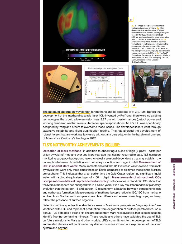
The tunable laser spectrometer (TLS) aboard the Mars Science Laboratory Curiosity rover—using lasers developed and space-qualified at MDL—has paved the way for semiconductor lasers to play an important role in future planetary science missions with applications in spectroscopy, laser altimeters, and metrology.“TLS has been an incredible success for MDL, the Instrument Division, and JPL. I am so very proud of the TLS team (design, fabrication, integration, and test) who have ensured that this instrument would continue working so well, for so long, and so far from home,” said Chris Webster, the TLS Principal Investigator. “After 5 years on Mars, TLS is alive and well, and continues to produce high-impact science on Curiosity. The instrument is performing exactly as it did some 6 years ago pre-ship, with no deterioration in performance or capability. As a result of its success, TLS is part of concept studies for New Frontiers Venus and Saturn Probe missions. We are currently building a mini-TLS for CubeSats and other small platforms under internal research and technology development funding, enabled by our successful mini-digital electronics efforts. As far as science, the TLS results have been the principal subject of six papers in the journal Science, and generated several hundred news stories across the world.”
LASERS ON MARS KEEP GOING
Mars’ Gale Crater is a fascinating place to explore because of the mountain of layered materials in the middle. The layers tell a story about what Mars was like in the past, perhaps spanning much of the history of the red planet.
SUCCESS STORYMDL 2016–2017
31
INSPIR
ATION
• INN
OVATIO
N • IM
PLEMEN
TATION
a
a§ The image shows concentrations of methane discovered on Mars. b§ A low-dissipation interband cascade (IC) laser fabricated at MDL inside a package designed specially for TLS. This device emits at 3.27 μm and is designed to target absorption lines of CH4 for in situ measurements. c§ NASA’s Curiosity Mars rover has detected fluctuations in methane concentration in the atmosphere, showing episodic high-level release and also a seasonal dependence to the background values, implying activity in the modern environment of Mars. d§ The NASA Exceptional Technology Achievement Medal is presented to Dr. Webster by Deputy Director Larry James and former Director Dr. Charles Elachi.
All measurements are below 1 part per billion
0 5 10 15 20 25 30
S. Autumn S. Winter S. Spring S. Summer
N. Spring N. Summer N. Autumn N. Winter
Detection of Mars methane: in addition to observing a pulse of high (7 ppbv—parts per billion by volume) methane over one Mars year ago that has not recurred to date, TLS has been monitoring sub-ppbv background levels to reveal a seasonal dependence that may establish the connection between UV radiation and methane production from organic infall. Measurement of D/H in ancient Mars water: Measurements showed that D/H values in water evolved from rock pyrolysis that were only three times those on Earth (compared to six times those in the Martian atmosphere). This indicates that at an earlier time the Gale Crater region had significant liquid water, with a global equivalent layer of ~150 m depth. Measurements of atmospheric CO2 isotope ratios on Mars at unprecedented accuracy: Isotope ratios in C and O in CO2 show that the Mars atmosphere has changed little in 4 billion years. It is a key result for models of planetary evolution that the carbon 13 and carbon 12 results form a balance between atmospheric loss and carbonate formation. Measurements of methane isotopic ratios in 13C/12C from methane evolved from Martian rock samples show clear differences between sample groups, and may reflect the presence of surface organics.
Detection of fine spectral line structures seen in Mars rock pyrolysis as “mystery lines” are identified with ClO and represent production from degradation of surface perchlorates. As a bonus, TLS detected a strong HF line produced from Mars rock pyrolysis that is being used to identify fluorine-containing minerals. These results and others have validated the use of TLS on future missions to Mars and other worlds. JPL’s commitment to the development of TLS and related devices will continue to pay dividends as we expand our exploration of the solar system and beyond.
The optimum absorption wavelength for methane and its isotopes is at 3.27 µm. Before the development of the interband cascade laser (ICL) invented by Rui Yang, there were no existing technologies that could allow emission near 3.27 µm with performances (output power and working temperature) that were suitable for space applications. MDL’s ICL was specifically designed by Yang and others to overcome those issues. The developed lasers went through extensive reliability and flight qualification testing. This has allowed the development of robust lasers that are working flawlessly without any degradation in the harsh environment of Mars since Curiosity’s landing in 2012.
TLS’S NOTEWORTHY ACHIEVEMENTS INCLUDE:
METHANE RELEASE: NORTHERN SUMMERMethane concentration
Parts per billion
b c d

JPL
| M
ICR
OD
EVI
CE
S L
AB
OR
ATO
RY
| 20
16-2
017
AN
NU
AL
RE
PO
RT
32
IN HIS WORDS
HOW DOES YOUR WORK EXTEND OR EXEMPLIFY THE IDEA THAT THE MOST COMPELLING NEW SCIENCE OF ANY ERA IS FOUND THROUGH ENABLING NEW MEASUREMENT CAPABILITY AND QUALITY?TODD • I can make it possible for new instruments to access higher precision of surface shape and positioning. This in combination with the unique detection capabilities of delta-doping will open new windows to astrophysics, planetary science, and Earth science.
WHAT DO YOU ENJOY MOST ABOUT WORKING AT MDL?TODD • At the MDL we have a growing collection of inspirational thinkers who already know how to solve the problems that haven’t happened yet. That is, in my opinion, what creates a truly effective research environment.
Dr. Jones is a member of the Advanced Detectors, Systems and Nanoscience group at the MDL. His role in the team is to prepare detector surfaces for delta-doping and to package photon and low energy particle detectors. His current research concentrates on detector science and new and custom packaging methods for future instruments.
Earth-based observatories, with their ability to continually improve performance with upgraded imagers, provide new and valuable astronomy. On-sky data on these facilities also serve as performance verification and validation of imaging technology. Custom-packaged 2D-doped (two-dimensionally doped, i.e., delta-doped and superlattice-doped) charge-coupled devices (CCDs) developed at MDL have now seen first light. The Wafer-Scale camera for Prime focus (WaSP), a collaboration between Caltech Optical Observatories (COO) and JPL, is the new prime focus imager for the 200-inch telescope, providing multiband color imaging from 320–1000 nm. WaSP was developed to replace the older Large-Format Camera (LFC) with a single high-
performance focal plane. The 2D-doped, fully depleted high-purity thick silicon devices delivered for WaSP have provided enhanced response across the near-ultraviolet to near-infrared (320–1000 nm). JPL’s delta-doping technology increased the U-band (<400 nm) sensitivity significantly beyond that of commercially available CCDs. Use of high-efficiency and high-stability 2D-doped arrays at Palomar-WaSP was partially motivated by the desire to obtain on-sky data as a pathfinder to a space-based UV Transient Astronomy mission concept called ULTRASAT.
In May 2016, the WaSP instrument with its low-noise, 6kx6k science CCD was installed on Palomar’s 200-inch telescope along with the JPL-provided guide and focus CCDs. To achieve the highest image quality, the instrument needs dedicated guide and focus CCDs to provide real-time feedback to the telescope tracking system and focus controls. The guide CCD, in particular, needs to have as high a sensitivity as possible. In response, JPL developed a custom-packaged, custom-coated delta-doped CCD based on an STA 3600 detector where both blue and red ends of the CCD response are significantly enhanced. Due to the tight space constraints in the WaSP dewar, these custom guide and focus CCDs also needed to be brought as close as possible to the science CCD. This required the development of a custom CCD package to reduce the detector footprint to the physical size of the detector die, with no wire-bonds or detector packaging outside that area. The packaging requirements also called for meeting tight tolerances on the final package thickness, to avoid shimming in the dewar to achieve focus. In the final configuration, all three CCDs (guide, focus, and science) are installed on a flexure mount in the correct focal plane positions within 20 microns across multiple devices, which is impressive.
After the successful delivery of these CCDs, Caltech Optical Observatories funded the production of five additional CCDs for the upcoming Zwicky Transient Facility instrument on the 48-inch Oschin Telescope at Palomar, which will conduct high-cadence sky-surveys for transient astronomical objects. WaSP also serves as a technology pathfinder for the Zwicky Facility. These five CCDs have been packaged and assembled, and are ready for delivery to integration and test.
TRULY FLAT, HIGH-PERFORMANCE FOCAL PLANE ARRAYS
TODD JONES
WaSP GUIDE AND FOCUS CCDS
CUSTOM PACKAGED2D-DOPED (DELTA-
DOPED AND SUPERLATTICE-
DOPED) CHARGE-COUPLED DEVICES
(CCDS) DEVELOPED AT MDL HAVE NOW SEEN FIRST LIGHT
AT PALOMAR.
a§ One of the WaSP detectors in a custom fixture for producing the non-coplanar wire-bonding.
b§ The unique non-coplanar wire-bonds of the WaSP detector.
c§ Close-up of the first prototype of non-coplanar wire-bonding.
d§ The WaSP prime focus camera with one large commercially available CCD and two of the WaSP guide and focus CCDs created by JPL.
e§ Colliding galaxies (NGC 7674 and NGC 7318) imaged with the advanced delta-doped CCDs.
f§ A special rig setup to put 6.2 mg of epoxy on the moated mechanical mount that will support the WaSP imager.
g§ One of the WaSP detectors being tested for surface planarity.

a b
d
c
33
INSPIR
ATION
• INN
OVATIO
N • IM
PLEMEN
TATION
Focal Plane Arrays: Ten years ago, I heard astronomer Paul Scowen complaining that the imaging detectors used in the focal planes of their instruments were out of plane and had huge gaps between them. The surfaces were lumpy with tens of microns from peak to valley. The focal plane consisted of mosaicked detectors packed tightly against each other, but still there were wide gaps separating the actual pixel arrays from one to the next. I began to think of ways to close the gaps and smooth out those bumps.
Throughout our development of various kinds of detector arrays (e.g., CCD and CMOS imaging detectors) we had devised different ways of conforming the sometime fragile membrane surface of the device to a very flat focus plane. In an earlier project, we had already invented a way to achieve flatness to within two microns. This flatness was accomplished using epoxy for attachment to a flat support surface. The epoxy thickness that we achieved was within ~6 µm, which confounded established rules dictating that successful attachment required 40-µm-thick epoxy bonds. This was a possible explanation for problems leading to commercially available “lumpy” detectors.
Beyond the limitations of conventional device fabrication tools: The challenges of achieving device closeness and narrow “gap” posed by WaSP required new, creative solutions to device packaging. To eliminate the gap due to wire-bonding, wires could go inward from the edge of the detector. This could be achieved by connecting the wires up the side of the mechanical mount, and tilt that inward so nothing sticks out over the edge. The challenge is that the existing wire-bonding machines could only connect across two parallel planes, whereas the custom package planes have a 60° tilt with respect to each other. By devising a tilt-and-bond scheme, we tucked the wires inward and successfully created four-side buttable packaging with narrow gaps.
Making Imagers Flat: The flatness was achieved by building an empirical model based on previous bonding experiments that had rendered flatness in small-area arrays. Using this model to guide the experimental trials, ultimately success was manifested in the creation of a moat to limit the epoxy flow and the precise placement and metering of a very non-viscous epoxy. The isolated epoxy patches merge void-free, producing a highly uniform bondline leading to flat-mounted imagers.
g f e

LARGE-FORMAT INFRARED FOCAL
PLANES ARE HIGHLY RELEVANT TO JPL
MISSIONS AND PROGRAMS.
JPL
| M
ICR
OD
EVI
CE
S L
AB
OR
ATO
RY
| 20
16-2
017
AN
NU
AL
RE
PO
RT
34
IN HIS WORDS
HOW DOES YOUR WORK EXTEND OR EXEMPLIFY THE IDEA THAT THE MOST COMPELLING NEW SCIENCE OF ANY ERA IS FOUND THROUGH ENABLING NEW MEASUREMENT CAPABILITY AND QUALITY?SARATH • As a technologist in MDL, I work with a team of engineers and technologists to develop new components which can enhance the capability of observational instruments. It’s a world-class facility that provides end-to-end capability for design, growth, fabrication, and test of various semiconductor devices.
WHAT HAVE BEEN YOUR GREATEST CHALLENGES WHILE WORKING AT MDL?SARATH • The challenge is to make better technology than we have today. We have proven this ability many times by breakthrough developments that enabled space missions previously thought to be impossible, which have helped to unravel the mysteries of the universe.
Dr. Gunapala is a senior research scientist, a JPL Fellow, and leads the Infrared Photonics Group at JPL. He works primarily with infrared semiconductor devices based on quantum wells, wires, dots, and superlattices. He has a special interest in studying novel “artificial” bandgap materials for infrared detectors and imaging focal planes.
Modern Earth science, planetary science, and astronomy increasingly depend on large-area focal plane array technology for high spatial resolution. There are a number of approaches being explored to meet this challenge. The new advances in epitaxial growth of III-V semiconductors on silicon could change how we explore the universe, both from the ground and from space.
NANOWIRE DETECTORSSARATH GUNAPALA
The use of silicon-based detector array technology in infrared instruments could represent a breakthrough in remote sensing. Prior to this work, monolithic silicon-based infrared detection technology was an elusive goal, mostly due to the inability to grow suitable defect-free light-absorbing semiconductor heterostructures with high quantum efficiency (QE) on silicon. Pallab Bhattacharya, the co-principal investigator, has pioneered catalyst-free growth of GaN nanowires and InGaN-GaN nanowire heterostructures on (001) silicon substrates. Single or multiple 2–3-nm-thick InxGa1-xN disks can be inserted in the GaN nanowires. The alloy composition in the disk region can be varied, thereby varying the effective bandgap. It has recently been discovered that quantum dots are formed in the InGaN disk in the nanowires. These quantum dots would be the main photon-absorbing regions in the proposed IR detector. The size and composition of the dots can be varied to tune the interband and intersubband transition energy in the disk (dot), and therefore the wavelength of light absorbed, over a wide range. A detector technology using III-nitride nanowires has not been previously demonstrated across a broad range of wavelengths.
MONOLITHIC III-NITRIDE NANOWIRE DETECTORS ON SILICON
a
a§ An image of a multi-band focal plane array on a cold finger of an observational instrument.
b§ An image of two megapixel and one VGA format focal plane array with a quarter for size comparison.
c§ Scanning electron microscope (SEM) image of the nanowire array.
d§ Heterostructure of green (λ~540nm) disk-in-nanowire.
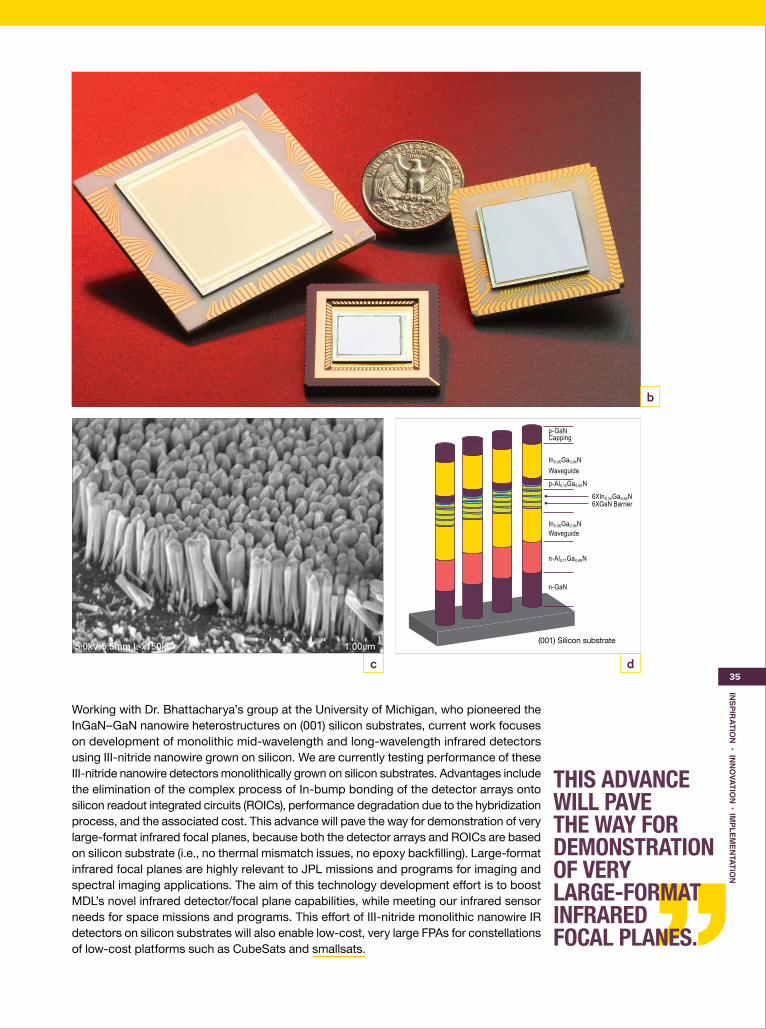
dc
b
35
INSPIR
ATION
• INN
OVATIO
N • IM
PLEMEN
TATION
THIS ADVANCE WILL PAVETHE WAY FOR DEMONSTRATION OF VERY LARGE-FORMAT INFRARED FOCAL PLANES.
Working with Dr. Bhattacharya’s group at the University of Michigan, who pioneered the InGaN–GaN nanowire heterostructures on (001) silicon substrates, current work focuses on development of monolithic mid-wavelength and long-wavelength infrared detectors using III-nitride nanowire grown on silicon. We are currently testing performance of these III-nitride nanowire detectors monolithically grown on silicon substrates. Advantages include the elimination of the complex process of In-bump bonding of the detector arrays onto silicon readout integrated circuits (ROICs), performance degradation due to the hybridization process, and the associated cost. This advance will pave the way for demonstration of very large-format infrared focal planes, because both the detector arrays and ROICs are based on silicon substrate (i.e., no thermal mismatch issues, no epoxy backfilling). Large-format infrared focal planes are highly relevant to JPL missions and programs for imaging and spectral imaging applications. The aim of this technology development effort is to boost MDL’s novel infrared detector/focal plane capabilities, while meeting our infrared sensor needs for space missions and programs. This effort of III-nitride monolithic nanowire IR detectors on silicon substrates will also enable low-cost, very large FPAs for constellations of low-cost platforms such as CubeSats and smallsats.

a b
JPL
| M
ICR
OD
EVI
CE
S L
AB
OR
ATO
RY
| 20
16-2
017
AN
NU
AL
RE
PO
RT
36
Dr. Wilson is a principal optical engineer leading the development of electron-beam-fabricated diffractive optics and imaging spectrometer gratings at JPL, including many for airborne and spaceborne flight instruments. He was awarded the NASA Exceptional Technology Achievement Medal and the JPL Lew Allen Award for his work.
Richard Muller is a microdevices engineer in charge of operating the MDL’s JEOL JBX 9500FS e-beam lithography system and associated tools. During his 29 years at JPL, he has operated three e-beam tools and has contributed to the development and delivery of many optical and electronic components for research and flight projects.
Gaining an understanding of the elemental composition of the Martian surface is a job best done close up. MDL is providing critical micro-optics for two instruments aboard the Mars 2020 rover to enhance the mission’s ability to deliver a deeper understanding of the elemental makeup of rocks and soil on the Red Planet.
MICRO-OPTICS FOR THE MARTIAN SURFACE
DANIEL WILSON | RICHARD MULLER
PIXL• The Planetary Instrument for X-ray Lithochemistry (PIXL) is an X-ray spectrometer that works at a microscopic level to rapidly identify the elements in rock and soil samples using X-ray fluorescence. The instrument also features a microscopic camera that can image individual grains, allowing scientists to match spectrometer measurements with visible characteristics. PIXL will greatly enhance the 2020 rover’s ability to seek signs of microbial life on Mars, past or present. In use, PIXL will focus an X-ray beam on each spot to be analyzed, then move the beam to another spot, working in a linear or grid pattern to produce a detailed map of the elements in the rock or soil target. To localize the instrument relative to the sample, and to map the topography of the surrounding area, PIXL’s Optical Fiducial Subsystem (OFS) uses two structured-light illuminators with a camera system. Critical to the OFS operation are micro-optic spot array generators that produce patterns of laser spots. The spot array generators are transmissive computer-generated hologram (CGH) gratings that are designed, electron-beam-patterned, and plasma-etched into glass in the MDL. Each unit cell of the two-dimensional CGH grating is made up of submicron square pixels, and when etched to the proper depth in glass, the surface relief pattern imparts a phase pattern on the laser beam, causing it to diffract into an array of spots with near equal intensity. The PIXL OFS then analyzes the pattern of spots to determine the three-dimensional topography of the rock to aid in instrument positioning.
SHERLOC• The Scanning Habitable Environments with Raman & Luminescence for Organics & Chemicals (SHERLOC) is an arm-mounted, deep-UV (DUV) resonance Raman and fluorescence spectrometer utilizing a 248.6-nm DUV laser and <100-micron spot size. SHERLOC enables non-contact, spatially resolved, and high-sensitivity detection and characterization of organics and minerals in the Martian surface and near-subsurface. The instrument goals are to assess past aqueous history, detect the presence and preservation of potential biosignatures, and support selection of return samples. In support of SHERLOC, the MDL is electron-beam fabricating gratings for the Raman and fluorescence spectrometer. Prototype gratings have been measured to produce near-theoretical-maximum diffraction efficiency at the 248.6-nm operating wavelength, and flight grating production is beginning.
a§ Mars 2020 PIXL spot array grating design (unit cell composed of 160-nm pixels, marked in red) and a scanning electron microscope (SEM) image of an e-beamefabricated grating etched into fused silica. b§ A scanning electron microscope (SEM) image of an e-beam-fabricated sinusoidal ultraviolet reflective grating for Mars 2020 SHERLOC.
PIXL RAPIDLYMEASURESELEMENTALCHEMISTRY ATSUBMILLIMETERSCALES BYFOCUSING ANX-RAY BEAM TOA TINY SPOT ONTHE TARGET ROCKOR SOIL ANDANALYZING THEINDUCED X-RAYFLUORESCENCE.

Conductionminiband
Heavy-holeminiband
Light-holeminiband
Electron barrier
Hole barrier
ContactContact Infrared absorber
Ec
Ev
GaSb InAs
hv hv
37
INSPIR
ATION
• INN
OVATIO
N • IM
PLEMEN
TATION
a b
a§ Energy-band diagram of a complementary barrier infrared detector (CBIRD) structure. The infrared absorber is surrounded by a unipolar electron barrier (blocking electrons only) on the left, and a unipolar hole barrier (blocking holes only) on the right. The complementary barriers serve to reduce dark current (noise), but allow photo-generated electrons and holes (signal) to travel unimpeded to the right and left electrical contacts, respectively.
b§ A close-up of the CBIRD infrared absorber section, consisting of an InAs/GaSb type-II superlattice (T2SL) where quantum mechanical effects lead to the formation of distinct minibands of energy levels. Optical transitions between the hole and the conduction minibands are used for infrared detection.
WIDE-APPLICATION INFRARED DETECTORS
DAVID TING
IN HIS WORDS
WHAT DO YOU ENJOY MOST ABOUT WORKING AT JPL / MDL? DAVID • The technical part of my work involves coming up with new device concepts and designs; I am very fortunate to be working among a group of highly talented and dedicated MDL colleagues who can turn ideas into working inventions. While we have transitioned the more mature areas of our patented technology to industry, we continue to conduct research in advanced infrared detectors for NASA’s needs, such as land imaging for future missions and observation of volcanism on Io and Venus. We are also working with JPL scientists and engineers on infusing our infrared imagers into airborne and satellite instrument for atmosphere and Earth science studies. Soon, the BIRD will fly!
Dr. Ting is a Senior Research Scientist and a Principal Member of Engineering Staff at JPL.His research in semiconductor physics and devices has led to over 230 publications and 12 patents. He is a Fellow of the SPIE.
Infrared detectors and imagers are valuable for more than just astronomy and planetary science. These sensitive devices have wide-ranging applications in meteorology, oceanography, geology, astronomy, archaeology, medicine, firefighting, law enforcement, national defense, environmental monitoring, and
industrial process monitoring. The MDL’s Infrared Photonics Technology group has been working to develop a new generation of high-performance, cost-effective infrared photodetectors and focal plane arrays with the flexibility to meet a variety of application requirements. Our detector technology is based on artificially designed multilayer semiconductor structures that exploit quantum effects to provide continuous adjustability in cutoff wavelength (the longest wavelength of electromagnetic radiation that can be detected effectively), while simultaneously delivering high signal-to-noise ratio. The development of this technology requires constant exploration and experimentation in design, material growth and characterization, and device fabrication and measurement. The well-maintained, state-of-the-art facilities in MDL are essential to our success.
THERMAL INFRARED FOCAL PLANE ARRAYS FOR NASA SUSTAINABLE LAND IMAGING The project focuses on demonstrating a high-performance, long-wavelength infrared (LWIR) focal plane array (FPA) technology with the flexibility to meet different possible future land imaging needs, including higher operating temperature for reduction in size, mass, power, and volume, compact instrumentation for small satellites, multispectral or hyperspectral imaging for richer science returns, and improved temporal and spatial resolution imaging. Previously, the choice of LWIR FPAs has been limited to either HgCdTe (MCT), or the quantum-well infrared photodetector (QWIP), each with its strengths and weaknesses. The type-II superlattice (T2SL) high operating temperature (HOT) barrier infrared detector (BIRD) developed at the MDL has recently emerged as an alternative that combines the high operability, spatial uniformity, temporal stability, scalability, producibility, and affordability advantages of the QWIP FPA with the superior quantum efficiency (QE) and dark current characteristics of the MCT detector. JPL is collaborating with L-3 CE (Cincinnati Electronics), a leading IR imaging systems manufacturer with a patented silicon-on-silicon FPA process that enables very large-format FPAs with high uniformity and operability. L-3 CE has already successfully integrated mid-wavelength infrared (MWIR) HOT-BIRD FPAs into imaging systems, and will collaborate with JPL to integrate an LWIR FPA into a compact sensor core with integrated dewar-cooler assembly (IDCA). The project is supported by the NASA Earth Science Technology Office (ESTO) Sustainable Land Imaging-Technology (SLI-T) Program. The goals of the program are to research, develop, and demonstrate new measurement technologies that improve upon our current land imaging capabilities, while at the same time reducing the overall program cost for future sustainable land imaging measurements.
OUR DETECTOR TECHNOLOGY IS BASED ON ARTIFICIALLY
DESIGNED MULTILAYER
SEMICONDUCTOR STRUCTURES.

RF MICROWAVE & MICRODEVICES ENGINEERDR. CECILE JUNG-KUBIAKDr. Jung-Kubiak joined JPL as a NASA Postdoctoral Fellow and is now a member of the Submillimeter Wave Advanced Technology group. Her research interests include the development of silicon micromachining technologies to build compact 3-D instruments and the miniaturization of micropropulsion systems.
What we do at MDL helps to answer the big questions about how stars and galaxies form, the possibility of life beyond our planet, the evolution of other worlds, and the health of Earth. Building instruments to enable these scientific investigations requires the development of new technologies, the invention of new devices, and novel assembly techniques. The path to success is filled with twists and turns, utter joy, and deep frustrations. But when we work together, keeping the ultimate goal in sight and the big picture in mind, this work can be a rewarding, inspiring, and humbling experience.One of my high school teachers once told me that I was too wild to ever succeed in science, and I am glad to have proved him wrong. What motivates me the most is the fact that seemingly crazy ideas could lead to a flight mission in the near future that may lead to new discoveries. At MDL, we have access to the best new technologies, and we are able to work with the smartest engineers and scientists. I am extremely proud to be part of that team. It helps bring out the best in me and pushes me to always go further, to not give up and to truly “dare mighty things.” Where do I see myself in 5 years? Probably still doing the same work that I love, while trying to inspire younger engineers and kids to dream big and to believe in themselves.
SCULPTING WITH IONS
MDL IS DEVELOPING NOVEL SILICON-BASED SUBMILLIMETER- WAVE RECEIVERS FOR FUTURE NASA MISSIONS.
JPL
| M
ICR
OD
EVI
CE
S L
AB
OR
ATO
RY
| 20
16-2
017
AN
NU
AL
RE
PO
RT
38
Microfabricated silicon needles for microfluidic electrospray propulsion (MEP) systems.
SUCCESS STORYMDL 2016–2017

39
INSPIR
ATION
• INN
OVATIO
N • IM
PLEMEN
TATION
d
f
g
h
e
Multipixel spectrometer arrays will open entire new vistas for the next generation of THz instruments, and MDL is developing novel silicon-based submillimeter-wave receivers for future NASA missions. Using deep reactive ion etching (DRIE), we can make ultracompact receivers by etching waveguide and complex structures in silicon bulk material, and integrating various active devices in a single silicon micromachined block. This technique provides better feature dimensional control and surface roughness than conventional machining, which in turn allows the design and implementation of novel components and their vertical integration in an ultracompact instrument package. With these techniques, we are not just reducing the size and volume of the instrument, we are also improving its sensitivity and overall performance.
With our unique silicon micromachined capabilities, we can now propose instruments operating at higher frequencies and with improved performance characteristics, such as the ability to resolve wind speed, temperature, pressure, and atmospheric composition of planets and planetary bodies in a single flight.
NASA has recently funded the development of a super-compact state-of-the-art submillimeter-wave radiometer/spectrometer, the PISSARRO instrument concept, under the MatISSE program for potential future orbiter missions to Mars, Venus, Titan, and other outer planets. PISSARRO will allow a large number of chemical species on planetary atmospheres to be detected at concentrations below one part per billion, using our newly developed silicon micromachining technology to provide a low-mass and highly integrated instrument.
SILICON MICROMACHINING FOR ADVANCED TERAHERTZ INSTRUMENTS
WITH OUR UNIQUE SILICON MICRO-MACHINED CAPABILITIES, WE CAN
NOW PROPOSE INSTRUMENTS OPERATING AT HIGHER FREQUENCIES
AND WITH IMPROVED CHARACTERISTICS.
d§ The entire PISSARRO instrument, small enough to fit into a shoe box.
e,f§ The 500–600-GHz spectrometer front end, with a close-up of the heart of the instrument showing all the silicon micromachined waveguide structures.
A 560-GHz mixer circuitry (g) and 560-GHz four-way power combined tripler circuitry (h) for the PISSARRO instrument.

JPL
| M
ICR
OD
EVI
CE
S L
AB
OR
ATO
RY
| 20
16-2
017
AN
NU
AL
RE
PO
RT
40
The light that reaches our telescopes from objects in space can be incredibly faint due to distance or low radiance, and scientists are continuously searching for better ways to observe these dim signals. Similarly, increasing levels of accuracy are sought for spectrometers and other critical instruments. The MDL has been pivotal in advancing the state of the art of such instrumentation through their microfabrication abilities and processes.
UNIQUE CAPABILITIES OF ATOMIC LAYER DEPOSITION (ALD) Ongoing development of UV, X-ray, infrared, and submillimeter telescopes and spectrometers will revolutionize our understanding of the formation and habitability of the solar system and beyond. While existing technology has allowed us to probe deep into space, materials and fabrication challenges still limit the sensitivity and capability of the detectors and instruments used in these investigations. MDL utilizes the precision and control afforded by atomic layer deposition (ALD) to substantially increase the capability of the instruments and detectors that scientists use to make new discoveries. ALD is a chemical technique that creates devices with control precision and flexibility at the angstrom scale. High-quality, pinhole-free films of a wide variety of materials can be assembled with extreme precision and uniformity over an arbitrarily large surface area.
In the MDL, ALD films have been employed in the coating, passivation, and fabrication of UV, infrared, and submillimeter detectors. ALD processes have also enabled the conformal coating of three-dimensional structures, an extremely challenging process that results in unique materials with excellent strength-to-weight ratios, tailorable surface-free energies (for contamination control on instruments), and metamaterial-like optical properties.
a
CRAFTING WITH ANGSTROM-LEVEL PRECISION
FRANK GREER
IN HIS WORDS
WHAT DO YOU ENJOY MOST ABOUT WORKING AT MDL?FRANK• I enjoy working on projects that may make it into space or onto another planet. There is no other job where my research could someday make an impact on our understanding of the universe. I also really like the ability to share what I do with the public, through journal articles, presentations, and the JPL open house. In my career in the semiconductor industry before JPL, a great deal of what I did had to be kept as a trade secret.
HOW DOES YOUR WORK EXTEND OR EXEMPLIFY THE IDEA THAT THE MOST COMPELLING NEW SCIENCE OF ANY ERA IS FOUND THROUGH ENABLING NEW MEASUREMENT CAPABILITY AND QUALITY?FRANK• The precision, confor-mality, and flexibility of atomic layer deposition has proven to be uniquely enabling for NASA/JPL applications. It has enabled world-record quantum efficiency in ultraviolet detectors, flexible ceramic materials, passivating layers for III-V IR detectors, and uniform superconducting detectors. Ultimately, these advances should enable new instruments and new discoveries.
Dr. Greer joined JPL in 2007, working in Division 38 in the MDL applying ChemE and semiconductor processing techniques to the fabrication of instrument components to support current and future NASA missions and reimbursable tasks. He currently works on the WFIRST CGI in collaboration with Division 32 and as a PI/CoI on various internally and externally funded R&D tasks to develop new materials and processes for next-generation instruments.
MDL UTILIZES THE PRECISION
AND CONTROL OF ATOMIC LAYER DEPOSITION TO
SUBSTANTIALLY INCREASE THE CAPABILITY OF
THE DETECTORSTHAT SCIENTISTS
USE TO MAKE NEW
DISCOVERIES.
1.6nm
High Q(106)
a§ Transmission electron microscope (TEM) image of a high-Q superconducting ALD TiN film with an engineered ALD Al2O3 interface.

b c
41
INSPIR
ATION
• INN
OVATIO
N • IM
PLEMEN
TATION
b§ Fully packaged Cassini delta-doped CCD with ALD-deposited anti-reflection coating achieving world-record quantum efficiency in the ultraviolet. c§ A frame-thinned Cassini imager shows the characteristic clover-like surface variations resulting from the device thickness being thinned to less than 20 μm. Red light reflected from the mirror surface below is transmitted through the thin membrane. d§ World-record quantum efficiency of Si CCD achieved with ALD-deposited AR coatings in the MDL. Note that this graph shows the performance of the device in images b and c. e§ Critical temperature measurement of a superconducting ALD TaN film. f§ TiN nanolattice-fabricated with ALD TiN in JPL/MDL. g§ Close-up of region indicated in figure f. h§ Passivating ALD oxide films deposited on InAs.
QE
(%)
Single layer AR coating on δ-doped CCDs
Wavelength (nm)
0 125
FUV Band 1100-200nm
FUV Band 2165-200nm
NUV Band 2240-300nm
NUV Band 1200-240nm
GALEX FUVGALEX NUV
13 nmBare
16 nm 23 nm 23 nm
*MgF2 result for thermally evaporated film
MgF2* A12O3 A12O3 HfO2
150 175 200 225 250 275 300
10
20
30
40
50
60
70
HfO2 plasma
Temperature (K)
Res
ista
nce
(Ω)
Temperature (K)
300
300
200
250
200
100100
150
0
0
50 0
5 7 9 11
100 200 300Resis
tanc
e (Ω
)
The ability of ALD to coat three-dimensional patterns will enable the synthesis of new types of mechanical and functional nano- and microstructures with unique strength-to-weight ratios and optical properties. ALD is an area of rapid growth at MDL. The ability of ALD to produce novel materials such as nanoalloys uniformly on large substrates could make the precise control and selection of superconducting transition temperature for a given detector more achievable with a wider variety of materials. In addition, ALD can coat the inside of holes that are tens of microns across and hundreds of microns deep and may ultimately enable MDL engineers to make hybridized superconducting devices with a higher fill factor than current approaches allow.
ALD is truly a fabrication process of the future that is occurring today, and empowering ever more fruitful missions of Earth observation, planetary science, and astrophysics.
HIGH-QUALITY, PINHOLE-FREE FILMS OF A WIDE VARIETY OF MATERIALS CAN BE ASSEMBLED WITH EXTREME PRECISION AND UNIFORMITY OVER AN ARBITRARILY LARGE SURFACE AREA.
d
e
f hg

a
b
a§ Dilution refrigerator used to cool detector arrays to 10 mK for performance characterization. b§ QCD array assembly showing the lens array to couple radiation and the detector array.
c§ Quantum capacitance signal displaying missing peaks (purple) due to absorption of a single photon.
c
JPL
| M
ICR
OD
EVI
CE
S L
AB
OR
ATO
RY
| 20
16-2
017
AN
NU
AL
RE
PO
RT
42
IN HIS WORDS
HOW DOES YOUR WORK EXEMPLIFY THE IDEA THAT THE MOST COMPELLING NEW SCIENCE OF ANY ERA IS FOUND THROUGH ENABLING NEW MEASUREMENT CAPABILITY AND QUALITY?PIERRE• The detector we are developing will enable observation of the formation of the first stars and galaxies in the universe. This is a capability that does not exist right now. Hopefully it will lead to many surprising discoveries.
WHAT DO YOU ENJOY MOST ABOUT WORKING AT MDL?PIERRE• I have been working at JPL since finishing my post-doctoral research, when I collaborated with the Superconducting Materials and Devices group at MDL. I work on researching the striking properties of small devices at very low temperatures in applications that are useful for astrophysics. This makes my work even more exciting, as it could lead to detectors used to advance fundamental knowledge about our universe.
Pierre Echternach is a member of the Superconducting Devices and Materials Group at JPL’s Microdevices Laboratory. He uses radio-frequency techniques to study mesoscopic superconducting devices at millikelvin temperatures. Current research concentrates on developing quantum capacitance detectors for applications in astrophysics.
A few years back, a team of engineers was working on a quantum computing project that utilized Cooper pairs, two electrons bound together in the superconducting state, for advanced computing. But electromagnetic fluctuations in the system repeatedly caused the bonds between the Cooper pairs to break. MDL researchers realized that this phenomenon could actually be useful if reversed—the device could be used to measure tiny amounts of radiation with incredible accuracy. The result is the extremely sensitive quantum capacitance detector (QCD). This device works in far-IR, a part of the spectrum of particular value to astronomers, since it is critical to understanding the formation and evolution of galaxies from their very beginnings. But working in these wavelengths is very challenging, since the small photon energies and extreme sensitivity required mean that even getting a single detector pixel at the target sensitivity is a major technical hurdle. The QCD has demonstrated the required sensitivity for future far-IR missions, and is capable of detecting individual far-IR photons.
COUNTING PHOTONS
PIERRE ECHTERNACH
Astronomers working in the far-IR must develop their own detector technology because this region of the spectrum has not been a focus of industrial development for commercial markets like detectors in the visible and near-IR. The small photon energies and extreme sensitivity required mean that even getting a single detector pixel at the targeted sensitivity is a major technical hurdle, let alone imaging arrays. Detection of single photons of 1.5 THz radiation has been demonstrated using the quantum capacitance detector (QCD). Previously demonstrated at JPL to have excellent noise equivalent power (NEP), with a NEP on the order of a few x 10–20 W/sqrt(Hz), the current implementation of the QCD uses a mesh absorber consisting of 50-nm-wide aluminum wires on a grid with 5x5 μm unit cells and 60x60 μm overall dimensions, which is fabricated by electron-beam lithography at the MDL.
Radiation generated by a thermal black body source filtered by 1.5 THz bandpass filters is coupled to the mesh absorber by Fresnel lenses also fabricated at the MDL. The absorption of a single photon breaks Cooper pairs in the absorber, creating a population of unpaired electrons that tunnel rapidly to a superconducting island connected to the absorber by a small tunnel junction. A single electron in the island suppresses the quantum capacitance peak, which is the baseline response of the device, and is thus easily detectable This QCD technology is also amenable to fabrication as arrays, and 500-pixel arrays currently under development in MDL will be able to transform the impacts of far-IR photons into images that may help to answer questions about the very origins of the universe.
DETECTION OF SINGLE 1.5-THz PHOTONS WITH THE QUANTUM CAPACITANCE DETECTOR

a b
43
INSPIR
ATION
• INN
OVATIO
N • IM
PLEMEN
TATION
a§ A CAD rendering of the fore-optics of the miniature open-path TLS. It uses flight heritage components/subassemblies in a compact, robust, and passively athermalized configuration.
b§ A miniature open-path TLS that uses Alerstam’s advanced optical scheme with an MDL-produced tunable laser for Mars methane sensing.
Amazing discoveries have come from the tunable laser spectrometer (TLS) aboard the Curiosity Mars rover since it landed in August 2012. Among these was the detection of methane on the Martian
surface. MSL’s TLS is a remarkable instrument, but in the years since its deployment, JPL has made great strides towards smaller laser spectrometers—1 kg or less—that are more sensitive and more robust, and that possess expanded capabilities. Among these are small atmospheric probes, landers, rovers, and smallsat/CubeSat implementations where gas abundances and isotope ratio measurements are needed. Making a smaller, robust, and more sensitive TLS is key to understanding the other worlds in our solar system.
The sensitivity of TLS instrumentation is limited not by light source intensity, since MDL’s semiconductor lasers produce high output power, but rather by optical interference fringes within the multipass cell. Moving away from the traditional Herriott cell optomechanical configurations in which spot-pattern overlap enhances optical fringes, new solutions were sought that still produce long pathlengths (meters) but with equidistant spot pattern spacings that lead to improved sensitivity.
Two sample cell configurations were developed, one to address the need for improved sensitivity and a second to reduce the sample gas amount needed (e.g., for comet sampling). The first configuration uses a long pathlength comparable to the original TLS, but with optical beam spots more evenly spaced to avoid optical fringes that otherwise limit sensitivity. This first configuration was tested both at room temperature and at Mars conditions in a thermal-vacuum chamber, to reveal that the optical fringes observed were a factor of 10 less than those in TLS so that this new configuration is 10 times more sensitive to gas detection. The complete instrument weighs only ~1 kg, but outperforms MSL’s TLS by a factor of 10 for methane detection, being able to detect 0.2 parts per billion in 1 hour. The second sample cell design used a cylinder-within-a-cylinder configuration to leave only a small volume in between that was sampled by the circular optical beam pattern. In theory, this spectrometer will need only 1/100th the gas amount for a measurement.
This miniature version is being considered as a payload addition for Mars mission concepts, including MarsDrop, microprobes designed to piggyback on larger landers. It is also a candidate for the SpaceX Red Dragon payload. Other potential applications include Discovery- and New Frontiers-class mission concepts that rely on multiple atmospheric probes to examine places like Venus and Saturn. Continuing miniaturization and improvements in sensitivity and reliability are the future of planetary exploration, and instruments such as the miniature TLS will revolutionize the exploration of distant worlds.
MINIATURIZING TUNABLE LASER SPECTROMETERS WITH IMPROVED SENSITIVITY
SMALLER, BETTER, TOUGHER
ERIK ALERSTAM
IN HIS WORDS
WHAT DO YOU ENJOY MOST ABOUT WORKING AT JPL?ERIK • On a day-to-day basis I focus on my own job and tasks, and sometimes forget the big picture. Then, when I meet a fellow space exploration enthusiast, or give a tour of JPL to a collaborator or friend, I’m reminded about the amazing missions we do together as an organization, and what a truly special place to work JPL is.
WHAT ELSE DO YOU THINK IS IMPORTANT TO TELL SCIENCE NEWS READERS, OR THE PUBLIC IN GENERAL?ERIK • I think it’s important to thank the public for their support for, and engagement in, NASA’s missions. In return, we work hard to explore the solar system and beyond, monitor the health of our own planet, and hopefully to inspire the public and the next generation of scientists, engineers, and artists. The work that we do sometimes takes several decades before it comes to fruition, and can make the benefits seem obscure. However, by pushing the boundaries of space exploration, not only do we learn more about our place in the universe, but we also create short-term benefits. For example, some of the technologies we develop find use here on Earth, making their way into everyday life. I hope you will continue to support us, and join us on this amazing adventure.
Dr. Alerstam’s areas of expertise include development of optical instruments and lasers, and various optical spectroscopic techniques with an emphasis on pico- and nanosecond resolved measurements.
MAKING A SMALLER, ROBUST, MORE SENSITIVE
TLS IS KEY TO FUTURE MISSIONS TO EXPLORE
AND UNDERSTAND OTHER WORLDS IN
OUR SOLAR SYSTEM.
LaserDetector assembly
Reference gas cellReference
detector assembly
Beam splitter

RF MICROWAVE ENGINEER JPL GUSTO PROJECT MANAGERDR. JOSE SILESDr. Siles’s areas of expertise include the development of ultracompact multipixel local oscillator sources and high-resolution receivers in the submillimeter-wave range for Earth science, planetary science, and astrophysics missions. In 2012, he received JPL’s Outstanding Postdoctoral Research award in technology, instrumentation ,and engineering and was the recipient of a Fulbright Postdoctoral Research Grant in 2010–2012.
The Stratospheric Terahertz Observatory (STO-2), a balloon-borne radio telescope featuring cutting-edge MDL submillimeter-wave technology, was launched from NASA’s Long Duration Balloon Facility (LDB) in Antarctica in December 2016. STO-2 looked for carbon, oxygen, and nitrogen in star-forming regions of our galaxy. Antarctica is a harsh continent, and assembling and preparing for flight one of the most advanced submillimeter-wave radio telescopes in the world, in just a few weeks, was certainly challenging. Having the opportunity to spend more than two months in one of the most beautiful places in the world, flying technology that you have developed , was an extremely rewarding once-in-a-lifetime experience. I am very inspired by the fact that the innovative technologies we develop at MDL will help humankind better understand how the universe evolves and how stars and planets form. The submillimeter-wave technology I work on at JPL is also used to develop instruments that are able to detect water in ocean worlds and analyze its composition, study the chemical composition of planet atmospheres, monitor Earth’s health, and even detect cancer. There is a unique team spirit at JPL. I love having the opportunity to work with such an amazing group of people from so many different cultures, and with so many great qualities, both personally and professionally. I learn something new from them every day and this is certainly priceless to me.
THE FIRST FLIGHT OF ROOM-TEMPERATURE, MULTI-PIXEL, FREQUENCY-MULTIPLIED LOs ABOVE 1 THz IN A STRATOSPHERIC BALLOON ENVIRONMENT.
JPL
| M
ICR
OD
EVI
CE
S L
AB
OR
ATO
RY
| 20
16-2
017
AN
NU
AL
RE
PO
RT
44
FROM ANTARCTICA TO THE STARS
STO-2 in flight a few minutes after launch during its ascent to the stratosphere (flight altitude ~128,000 feet).
SUCCESS STORYMDL 2016–2017

45
INSPIR
ATION
• INN
OVATIO
N • IM
PLEMEN
TATION
a§ STO-2 launch configuration (from left to right: Helium balloon, parachute, launch vehicle and payload).
b§ Close-up view of the 4-pixel 1.9 THz local oscillator delivered by JPL.
c§ STO-2 “first light” [CII] integrated intensity map of a small region in NGC 3567.
d§ STO-2 payload with solar panels attached, ready for launch. It is ~22 ft wide and ~34 ft tall and weighs ~5000 lbs.
The Stratospheric Terahertz Observatory (STO-2) is a NASA-funded, balloon-borne 80-cm radio telescope consisting of five high-resolution heterodyne superconductive receivers to observe carbon ([CII] line at 1.9 THz), nitrogen ([NII] line at 1.46 THz), and oxygen ([OI] line at 4.7 THz) in our galaxy. These tracers are key to understanding the processes governing the formation of interstellar clouds and stars, which is crucial for unraveling the evolution of galaxies.
Carried by a ~400-ft-diameter helium balloon, STO-2 remained operative throughout its three-week baseline mission, gathering data 24 hours a day. Antarctica is an ideal location for balloon-borne telescopes since the polar anticyclone keeps the payload circling the continent and makes it possible to land and recover the instrument once the mission is completed.
JPL delivered state-of-the-art four-pixel frequency- multiplied local oscillator (LO) systems for the [CII] and [NII] receivers featuring Schottky diode–based frequency multipliers. Local oscillators are the most critical components of these receivers and their fabrication at the MDL requires submicron precision. Unlike the superconducting detectors, the LOs were mounted outside the cryostat and totally exposed to the environment during launch, ascent, and mission operations, which made the design much more challenging. The flight of STO-2
was the first time room-temperature, multi-pixel frequency-multiplied local oscillator sources above 1 THz have been successfully flown and operated in a stratospheric balloon environment. This confirms JPL’s leadership in the field and its ability to deliver multipixel LO sources for future NASA missions and platforms, such as SOFIA and the Cosmic Origins Space Telescope.
STO-2 is a NASA-funded program led by the University of Arizona, with JPL, the Applied Physics Laboratory (APL), Arizona State University (ASU), and the Dutch Space Agency (SRON), as Co-I institutions.
Based on the success of STO-2, NASA recently funded a follow-on mission: the Galactic/Extra-Galactic Ultra-long-duration Stratospheric Terahertz Observatory (GUSTO). GUSTO, a NASA Explorer Mission of Opportunity, will feature 24 receivers total (eight per band) and will be launched from LDB in December 2021. It will be carried by NASA’s brand-new Ultra Long Duration Balloon with a planned mission of 100 days.
THE STO-2 RADIO-TELESCOPE SUCCESSFULLY LAUNCHED FROM ANTARCTICA
a
b
d
c
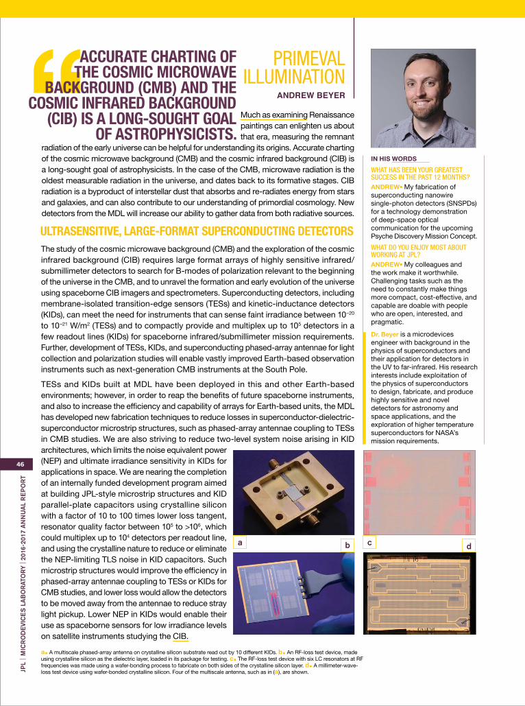
b dca
JPL
| M
ICR
OD
EVI
CE
S L
AB
OR
ATO
RY
| 20
16-2
017
AN
NU
AL
RE
PO
RT
46
IN HIS WORDS
WHAT HAS BEEN YOUR GREATEST SUCCESS IN THE PAST 12 MONTHS? ANDREW• My fabrication of superconducting nanowire single-photon detectors (SNSPDs) for a technology demonstration of deep-space optical communication for the upcoming Psyche Discovery Mission Concept.WHAT DO YOU ENJOY MOST ABOUT WORKING AT JPL? ANDREW• My colleagues and the work make it worthwhile. Challenging tasks such as the need to constantly make things more compact, cost-effective, and capable are doable with people who are open, interested, and pragmatic.
Dr. Beyer is a microdevices engineer with background in the physics of superconductors and their application for detectors in the UV to far-infrared. His research interests include exploitation of the physics of superconductors to design, fabricate, and produce highly sensitive and novel detectors for astronomy and space applications, and the exploration of higher temperature superconductors for NASA’s mission requirements.
Much as examining Renaissance paintings can enlighten us about that era, measuring the remnant
radiation of the early universe can be helpful for understanding its origins. Accurate charting of the cosmic microwave background (CMB) and the cosmic infrared background (CIB) is a long-sought goal of astrophysicists. In the case of the CMB, microwave radiation is the oldest measurable radiation in the universe, and dates back to its formative stages. CIB radiation is a byproduct of interstellar dust that absorbs and re-radiates energy from stars and galaxies, and can also contribute to our understanding of primordial cosmology. New detectors from the MDL will increase our ability to gather data from both radiative sources.
PRIMEVAL ILLUMINATION
ANDREW BEYER
ACCURATE CHARTING OF THE COSMIC MICROWAVE
BACKGROUND (CMB) AND THE COSMIC INFRARED BACKGROUND
(CIB) IS A LONG-SOUGHT GOAL OF ASTROPHYSICISTS.
The study of the cosmic microwave background (CMB) and the exploration of the cosmic infrared background (CIB) requires large format arrays of highly sensitive infrared/submillimeter detectors to search for B-modes of polarization relevant to the beginning of the universe in the CMB, and to unravel the formation and early evolution of the universe using spaceborne CIB imagers and spectrometers. Superconducting detectors, including membrane-isolated transition-edge sensors (TESs) and kinetic-inductance detectors (KIDs), can meet the need for instruments that can sense faint irradiance between 10–20 to 10–21 W/m2 (TESs) and to compactly provide and multiplex up to 105 detectors in a few readout lines (KIDs) for spaceborne infrared/submillimeter mission requirements. Further, development of TESs, KIDs, and superconducting phased-array antennae for light collection and polarization studies will enable vastly improved Earth-based observation instruments such as next-generation CMB instruments at the South Pole.
TESs and KIDs built at MDL have been deployed in this and other Earth-based environments; however, in order to reap the benefits of future spaceborne instruments, and also to increase the efficiency and capability of arrays for Earth-based units, the MDL has developed new fabrication techniques to reduce losses in superconductor-dielectric-superconductor microstrip structures, such as phased-array antennae coupling to TESs in CMB studies. We are also striving to reduce two-level system noise arising in KID architectures, which limits the noise equivalent power (NEP) and ultimate irradiance sensitivity in KIDs for applications in space. We are nearing the completion of an internally funded development program aimed at building JPL-style microstrip structures and KID parallel-plate capacitors using crystalline silicon with a factor of 10 to 100 times lower loss tangent, resonator quality factor between 105 to >106, which could multiplex up to 104 detectors per readout line, and using the crystalline nature to reduce or eliminate the NEP-limiting TLS noise in KID capacitors. Such microstrip structures would improve the efficiency in phased-array antennae coupling to TESs or KIDs for CMB studies, and lower loss would allow the detectors to be moved away from the antennae to reduce stray light pickup. Lower NEP in KIDs would enable their use as spaceborne sensors for low irradiance levels on satellite instruments studying the CIB.
ULTRASENSITIVE, LARGE-FORMAT SUPERCONDUCTING DETECTORS
a§ A multiscale phased-array antenna on crystalline silicon substrate read out by 10 different KIDs. b§ An RF-loss test device, made using crystalline silicon as the dielectric layer, loaded in its package for testing. c§ The RF-loss test device with six LC resonators at RF frequencies was made using a wafer-bonding process to fabricate on both sides of the crystalline silicon layer. d§ A millimeter-wave-loss test device using wafer-bonded crystalline silicon. Four of the multiscale antenna, such as in (a), are shown.

47
INSPIR
ATION
• INN
OVATIO
N • IM
PLEMEN
TATION
a§ Contemplating ancient artifacts such as this seventh-century burial mask of an Anglo-Saxon king can provide JPL engineers with perspective as they cope with difficult technical challenges. b§ Two high-power Schottky diode 183-GHz frequency doublers, fabricated in the MDL, and mounted in a power-combining metal waveguide block.
Spacecraft electronics have long pre-sented unique challenges to engineers seeking to make them smaller, more sensitive, cooler in operation, and less power-hungry. JPL has a long history of designing, building, testing, and flying advanced electronic components that
overcome these limitations. Recent developments at the MDL have led to new terahertz-frequency domain Schottky diodes that form the heart of high-frequency RF radiometers and heterodyne spectrometers. These devices have already led to new discoveries about the extent of Earth’s ozone hole, the isotopic composition of comets, and star formation in our galaxy. Now, these advanced RF devices are being leveraged as moderate power sources in radar applications for national security as well as Earth and planetary science.
KEN COOPERa
IN HIS WORDS
WHAT DO YOU ENJOY MOST ABOUT WORKING AT JPL?KEN• I enjoy the variety of technical challenges that working at JPL entails. Although I have moved far from my roots in graduate school as an experimental condensed-matter physicist, my engineering work is still based on the themes of cutting-edge instrumentation development, experimentation and data analysis, communi-cating results, and organizing teams and projects to reach milestones. Looking to my future at JPL, I hope to lead the maturation to flight readiness of millimeter- and submillimeter-wave technology, as it pertains specifically to radar remote sensing. In my spare time, I have recently been reading about Britain and Europe in the Dark Ages, and was thrilled to visit the Sutton Hoo exhibit, a showing of ancient artifacts found in Britain, during a recent conference for the European Microwave Week in London. I have found that contemplating artifacts such as the seventh-century burial mask of an Anglo-Saxon king, shown at that exhibit, has provided me with new perspectives as I work to overcome difficult technical challenges at MDL.
Dr. Cooper has led research and development efforts for both national security and Earth and planetary science. These include component and system development for standoff terahertz imaging, differential radar for humidity measurements inside clouds, and a combination radar/spectrometer for probing cometary jet dynamics.
Among the most exciting radar concepts to employ millimeter-waves is that of differential absorption radar to profile the absolute humidity inside of upper-tropospheric ice clouds. Better characterization of these clouds will improve weather and climate models, which currently rely on passive, radiometric measurements that are less accurate when clouds obscure the sought-after signals. A widely tunable millimeter-wave radar, on the other hand, can utilize ice-cloud scattering specifically by measuring relative signal absorption over the flank of water’s 183-GHz molecular absorption line.
However, generating sufficient power to enable practical atmospheric radar measurements at 183 GHz is very challenging, especially while exclusively using compact and low-power semiconductor devices. The MDL is developing high-power-handling Schottky diode frequency-doubler devices that, when combined in a compact waveguide package, can generate up to 0.5 W of continuous power with about 20% conversion efficiency. Achieving these results has required new THz design paradigms, such as the use of thicker substrates for heat dissipation and on-chip power-combining topologies for efficient frequency conversion. A new task has just begun under the NASA Earth Science Office’s Instrument Incubator Program (IIP) to measure humidity inside clouds using an airborne 183-GHz differential absorption radar. With that support, and their successful fabrication in the MDL, JPL’s high-power Schottky diodes will be scheduled for their next flight in 2019.
ADVANCED FREQUENCY MULTIPLIERS FOR RADAR SOUNDERS
b
ELECTRONICS FOR SPACE
THESE DEVICES HAVE ALREADY LED TO NEW DISCOVERIES ABOUT THE EXTENT OF EARTH’S OZONE HOLE, THE ISOTOPIC COMPOSITION OF COMETS, AND STAR FORMATION IN OUR GALAXY.

JPL
| M
ICR
OD
EVI
CE
S L
AB
OR
ATO
RY
| 20
16-2
017
AN
NU
AL
RE
PO
RT
48
a
IN HIS WORDS
WHAT DO YOU ENJOY MOST ABOUT WORKING AT MDL? ALEX • My greatest satisfaction from working at the MDL stems from constantly being surrounded by the most motivated and talented individuals in my field. It takes a special community of like-minded scientists and engineers to form a creative environment. Daily conversations, debates, and simple day-to-day interactions with my colleagues at MDL have pushed me to think harder not only about my work, but about the goals of the greater scientific community.
WHAT HAVE BEEN YOUR BIGGEST SUCCESSES WHILE WORKING AT JPL? ALEX • The most interesting part of my work at MDL is the path we have taken from transforming recent scientific discoveries in academia to advance technology. For example, we have succeeded in utilizing newly developed artificial materials, called superlattices, to improve infrared technology for Earth and planetary applications. Our work in infrared technology will advance remote sensing instruments by increasing their sensitivity and spatial resolution, and reducing their size and mass.
This breakthrough will enable development of new instruments for small satellites and UAVs. My recent work at the Microdevices Laboratory at JPL is the culmination of over 20 years of lab work, research, and intensive study of semiconductor devices. My passion for science was born out of innate curiosity about the world around me and it is still driving my research interests.
Dr. Soibel worked on the development of quantum cascade lasers for the tunable laser spectrometer for Mars Science Laboratory, and is currently engaged in the development of infrared imagers for various space and Earth based applications. He has co-authored more than 50 refereed articles and four book chapters.
A common theme at MDL and NASA is the drive for more sensitive detectors, especially in the mid- and long-wavelength infrared (MWIR and LWIR) spectral bands, which are critical to both Earth and planetary science. But instrumentation covering these spectral ranges requires complex cryogenic cooling to achieve the desired performance. Detectors operating at higher temperatures will enable replacement of large and heavy mechanical coolers with compact single-stage thermoelectric coolers.
The higher operating temperature can be achieved by integrating detectors with microlenses. A new class of lenses, called flat lenses, utilizes unique shapes that allow them to provide distortion-free imaging. Flat lenses have been developed at the MDL, and are engineered at subwavelength scales to provide desired wavefront of transmitted light. Until recently, infrared wavelengths have been a challenge for these kinds of lenses, but this is changing.
FLATTER LENSES
ALEXANDER SOIBEL
High operating temperature for detectors can be achieved by using optical concentrators that increase optical collection area while keeping detectors’ volume constant. The most common type of optical concentrator is a spherical microlens, but this technology is not well developed in mid- and long-wavelength infrared. Recently, a new class of optical components dubbed metasurfaces has been developed, based on inhomogeneous arrays of optical resonators with subwavelength separation. By accurately designing the properties of each element of the array, the wavefront of scattered or transmitted light can be reshaped and redirected at will depending on the design. The flat lenses are extremely thin, lightweight, and free from spherical aberration when compared with conventional refractive lenses.
We are working with a pioneer of flat lens development, Professor Federico Capasso at Harvard University, to extend flat lens technology into mid- and long-wavelength infrared spectral ranges. Our current project focuses on the development of a flat lens covering the 3–5-µm spectral band. Shown below is a scanning electron microscope (SEM) image of a flat lens designed by the Harvard group, fabricated on GaSb substrate at MDL using electron-beam lithography and dry etching. The lens consists of rods with subwavelength diameters varying across its diameter, which results in modulation of the transmitted light wavefront and focusing. The lens is 30 microns in diameter, and the designed focal length is about 100 µm, which makes it compatible with focal plane array architectures. We are currently testing performance of these lenses and will monolithically integrate them with single-pixel detectors and focal plane arrays in the near future.
Metamaterial flat lens development will greatly benefit instruments for outer planet missions as well as small satellites for Earth observations.
INFRARED DETECTORS MONOLITHICALLY INTEGRATED WITH FLAT LENSES
A NEW CLASS OF LENSES, CALLED
FLAT LENSES, UTILIZES UNIQUE
SHAPES THAT ALLOW THEM
TO PROVIDE DISTORTION-FREE
IMAGING.
a§ Scanning electron microscope (SEM) image of four flat lenses fabricated on GaSb substrates. The lens diameter is 30 microns and focal length is estimated to be 100 microns.

IN HIS WORDS
HOW DOES YOUR WORK EXTEND OR EXEMPLIFY THE IDEA THAT THE MOST COMPELLING NEW SCIENCE OF ANY ERA IS FOUND THROUGH ENABLING NEW MEASUREMENT CAPABILITY AND QUALITY?KARL• New technologies have enabled measurements previously thought not possible, and to perform these measurements with unprecedented accuracy. An example of this is the WFIRST coronagraph masks being fabricated at MDL. These masks enable the imaging of exoplanets, and thus to take spectra of their atmospheres. This could very well lead to the first detection of extraterrestrial life signatures.
Dr. Yee is a senior technologist in the Nano and Micro Systems group, with expertise in MEMS design, fabrication, and packaging processes. His primary area of research is on resonant vibratory inertial sensors. He has been the principal investigator on several programs for NASA, DARPA, and the Army.
Did you know that Mars appears to have earthquakes (referred to as “Marsquakes” on that planet)? Other rocky bodies in our solar system may have similar motions within their crust. Seismometers are critical instruments to understanding the geophysical dynamics of these fascinating bodies. Sensors designed to monitor
surface motions from landers have been part of the planetary exploration arsenal since the Viking Mars landers of the 1970s, but new developments have resulted in miniaturized designs that have improved sensitivity. These new devices are also more rugged than their predecessors, and require less delicate handling during landing—they can be released by orbiters to make hard landings on other worlds and return data for extended periods.
EXTRATERRESTRIAL EARTHQUAKES
KARL YEE
Inertial sensors utilize the lagged motion of a “proof mass” due to its inertia. Relative motion between the proof mass and the case of the sensor allows measurement of dynamic variables such as acceleration and rotation. MEMS inertial sensor development at JPL has a rich history. The highest performance MEMS gyroscope in the world is the JPL-developed disc resonator gyroscope (DRG). The development of this device was funded by industry and DoD, and the device has now been commercialized. Pioneering research at JPL showed the importance of resonator geometry and material selection in determining ultimate device sensitivity.
Current inertial MEMS research at JPL is focused on seismometers. Sensitive seismometers are critical for detecting faint motions deep within planetary bodies that can be used to reconstruct composition and temperature structure, while also revealing fundamental processes such as plate and ice tectonics, volcanism, ocean waves, ice flow, geysers, and more. In the coming years, NASA will launch a series of missions to explore the icy moons of Jupiter and Saturn that are believed to have subsurface oceans, in search of conditions for life in the outer solar system. Seismology can have a key role in those missions for determining both the deep and shallow interior structure and material properties of these ocean worlds, necessary for determining their ability to harbor life.
Traditional seismometers rely upon a large proof mass and a soft suspension system for high sensitivity. However, such a device is intrinsically very fragile. Thus, all space-based seismometers to date have required deployment using a soft lander. A novel MEMS seismometer under development at JPL is high shock-tolerant, and utilizes electrostatic spring softening to circumvent the performance limitations of having a small proof mass and a stiff suspension system. Such sensors could be dropped from orbiters, enabling the establishment of low-cost seismic networks on rocky planets and icy moons.
ZERO FREQUENCY RESONANT (ZEFR) MEMS BROADBAND SEISMOMETER
MINIATURE SEISMO-METERS UNDER
DEVELOPMENT AT MDL WILL ENABLE
THE DEPLOYMENT OF PLANETARY SEISMIC
NETWORKS.
49
INSPIR
ATION
• INN
OVATIO
N • IM
PLEMEN
TATION
a§ Precision navigation is enabled by JPL’s miniature disc resonator gyroscope (DRG).
b§ Vacuum-packaged inertial sensor.
c§ Shock-tolerant seismometers can be deployed via penetrators such as the Deep Space 2 (DS2) New Millennium Mars probes.
d§ Concept for deployment of a network of seismic sensors using penetrator spacecraft.
a b c d

MDL TECHNOLOGISTDR. APRIL JEWELLApril Jewell is a surface scientist with degrees from Tufts University (PhD) and George Washington University (BS); she came to MDL in 2012. Her research interests include the design, development, and implementation of advanced surface passivation techniques and device-integrated optical coatings for silicon-based imagers.
At the heart of NASA’s optical space telescopes and instruments are detectors that transform light into digital images with exceptional sensitivity, resolution, and dynamic range. Better sensitivity to dim and distant objects, as well as resistance to the ravages of space radiation, are desirable traits in a detector, as they have a direct and positive impact on a mission’s science return and cost. MDL is at the forefront of developing high-performance detectors that will lead to a better understanding of the universe around us. JPL-invented, two-dimensionally-doped (2D-doped) silicon detectors—including delta-doped and superlattice-doped detectors—offer high durability, high stability, and high sensitivity to wavelengths spanning the ultraviolet, visible, and near-infrared spectral regions. The 2D-doped detector technology has been advanced to the point that it is now baselined for a variety of mission concepts and platforms, including space telescopes, imaging spectrometers, CubeSat-based missions, and Explorer-class missions. The history of detector development for the Hubble Space Telescope illustrates one of the key challenges in achieving science-grade performance with imaging detectors. The charge-coupled devices (CCDs) produced for Hubble’s Wide-Field and Planetary Camera exhibited unstable response due to poor surface passivation; this prompted an intensive internally funded program to develop passivation techniques that would yield stable detectors. MDL’s delta-doping processes emerged from this effort, which led to the development of multilayer delta-doping, also known as superlattice-doping. These technologies enhance the stability and robustness of silicon-based detectors.
JPL
| M
ICR
OD
EVI
CE
S L
AB
OR
ATO
RY
| 20
16-2
017
AN
NU
AL
RE
PO
RT
50
PULLING LIGHT FROM THE DARKNESS
The central star (HD62166) in planetary nebulae NGC 2440 is one of the hottest known white dwarfs at ~219,000 K, and emits strongly in the ultraviolet. This image was obtained by the Hubble Space Telescope’s Wide-Field and Planetary Camera 2 using Lumogen®-coated CCDs to downconvert UV photons to visible wavelengths. MDL’s recent advances in UV-enhanced silicon detectors achieve far better UV sensitivity with improved stability.
SUCCESS STORYMDL 2016–2017

51
INSPIR
ATION
• INN
OVATIO
N • IM
PLEMEN
TATION
Solid-state detector arrays, especially silicon imaging arrays, are ubiquitous. Spaceborne applications of these imagers include astronomy and astrophysics, Earth observations, laser communications, and star trackers; in fact, most present-day NASA missions use silicon-based detectors for imaging or spectroscopy. Operation in space brings the additional challenge of dealing with radiation effects. For example, protons cause displacement damage within the silicon lattice, resulting in stable defects or “traps” within the device [c]. These traps accumulate over time and lead to increased dark current, hot pixels, and reduced charge transfer efficiency; all of which adversely affect performance and science return. The effects of radiation damage can be partially mitigated through the use of onboard shielding—a physical barrier meant to protect the detector—and inflight annealing—heating the detector to reduce the number of hot pixels. A more reliable approach is to alter the device structure itself to produce “rad-hard” detectors that are intrinsically less susceptible to radiation damage. This last approach is an area of active research at MDL.
SWITCHING POLARITY ON NANOENGINEERED SURFACES FOR RAD-HARD DETECTORS
DELTA-DOPED ARRAYS, INVENTED IN THE EARLY 1990s, EXHIBIT 100% INTERNAL QUANTUM EFFICIENCY, OFFERING THE HIGHEST SENSITIVITY AVAILABLE WITH A SILICON-BASED DETECTOR.
At MDL, we have developed and demonstrated 2D-doping processes that are universally applicable to a variety of detector architectures, including CCDs, complementary metal-oxide-semiconductor (CMOS) , and avalanche photodiodes. The broad applicability of our processing approach means that different missions, which emphasize different detector performance parameters, can all take advantage of the benefits of delta-doping. For example, CMOS imaging arrays offer a faster and more flexible readout architecture, whereas some CCDs offer high signal-to-noise for photon-counting applications. Additionally, to respond to the needs of larger-aperture telescopes, which require both larger detector arrays as well as a larger number of these arrays, MDL acquired a high-throughput molecular-beam epitaxy (MBE) machine capable of batch processing wafers up to 200 mm in diameter. In 2014, MDL successfully demonstrated wafer-scale delta-doping of back-illuminated CMOS imaging detectors, thus paving the way for large-scale production of high-performance detectors for space and commercial applications.
a
a§ JPL’s delta-doping and superlattice-doping processes can be applied at the wafer level for substrates as large as 8 inches in diameter.

The active region of a silicon-based detector is composed of lightly doped epitaxial silicon, and within this region is a buried channel of dopants that are either n-type (e.g., phosphorous) or p-type (e.g., boron), depending on detector design. MDL’s superlattice-doped detectors incorporate multiple delta layers for the elimination of trapping through improved quantum exclusion [d], offering a vast improvement in stability against damaging radiation over conventional devices. The majority of the advancements with 2D-doped detectors have been demonstrated using a p-type dopant in n-channel devices; however, the mechanism of radiation-induced trap formation has a lower probability in p-channel devices, resulting in higher radiation tolerance of the p-channel architecture. Thus, p-channel devices are favored for space environments, and highlight the need to develop n-type 2D-doping processes.
We previously demonstrated single-layer, n-type delta-doping, showing that the techniques proven for p-type delta-doping are applicable to n-type delta-doping. In an ongoing internally funded program, we are working to advance this proof-of-concept demonstration to the more complex, superlattice-doped structures for radiation-tolerant p-channel devices. These improved detector arrays will be far more sensitive and stable than their non-delta-doped predecessors, and will open new vistas in astronomical and astrophysical exploration.
db§ Dr. Jewell adjusts the camera for RHEED observations, an important in situ diagnostic used to monitor the MBE-based 2D-doping process. (RHEED: Reflection High-energy Electron Diffraction)
c§ Proton-induced displacement damage results in vacancies within the device’s crystal lattice and leads to increased noise and instability.
d§ This simulated band-structure of the MBE-grown superlattice shows a near-surface quantum well that effectively eliminates carrier trapping at the interface, resulting in high sensitivity and stable performance.
c
Proton
Displacement damage
N or P channel dopant region
Activesilicon
MBE-grown superlattice
Depth (nm)
Interf
ace d
ensit
y (cm
–2 eV–1 )
silicon detectorMBE-grown superlattice
SiO2
Cond
uctin
g-ba
nd ed
ge (e
V)
V= Vacancy
V
VVV
MDL’S SUPERLATTICE-DOPED DETECTORS OFFER A VAST IMPROVEMENT IN STABILITY AGAINST DAMAGING RADIATION OVER CONVENTIONAL DEVICES.
JPL
| M
ICR
OD
EVI
CE
S L
AB
OR
ATO
RY
| 20
16-2
017
AN
NU
AL
RE
PO
RT
52
b

a cb
Inte
nsity
(a.u.
)
Inte
nsity
(a.u.
)
Wavenumber (cm-1)
35 cm-1
750 fsWavenumber (cm-1)
Delay (ps)
2740
2774 2775 2776 2777 2778
2750 2760 2770 2780 2790 -0.75 -0.50 -0.25 0.25
876543210
0.50 0.75-0.00
Inte
nsity
auto
-cor
relat
ion (a
.u.)
53
INSPIR
ATION
• INN
OVATIO
N • IM
PLEMEN
TATION
Precision spectroscopy has long been one of the most valued tools in the planetary scientist’s lineup. Conventional methods have yielded amazing scientific results, but new developments in laser spectroscopy promise far greater data returns. Ultrafast laser spectroscopy, which operates at the level of atoms and molecules, depends on very precise tuning of the laser’s wavelength. Optical frequency combs, composed of a series of discrete, equally spaced lines, have quickly become the standard for precise measurements of frequency and time and are revolutionizing precision spectroscopy.
WELL-TUNED LASERS
MAHMOOD BAGHERI
IN HIS WORDS
WHAT DO YOU ENJOY MOST ABOUT WORKING AT MDL OR JPL?MAHMOOD • I like exchanging ideas with smart people and working with other creative minds around me and making new things happen.
WHAT ASPECT OF YOUR WORK MAKES YOU THE MOST PROUD?MAHMOOD • Mentoring new people at JPL/MDL. It helps new members feel comfortable at work and be prepared to take on challenging tasks.
Dr. Bagheri is a microdevices engineer at the Jet Propulsion Laboratory. During his time at JPL, he has pioneered a new class of optical frequency combs operating in the 3-4-µm wavelength range and flat optical components based on subwavelength optical gratings. His areas of expertise include nanophotonic integrated circuits and miniaturization of photonic components.
Optical frequency combs have become enabling tools for an increasing number of applications such as attosecond (1×10⁻¹⁸ of a second) science, optical waveform generation, remote sensing, microwave synthesis, optical communications, and astrophysics. Recently, dual-frequency spectroscopy has emerged as an attractive application of frequency combs, as it offers higher measurement sensitivities at a fraction of the time compared to traditional Fourier spectrometers. Therefore, extending optical frequency combs into the mid-infrared has broad implications for precision spectroscopy, as a large number of molecules undergo strong vibrational transitions in this range, and optical combs enable real-time and large-dynamic-range spectroscopy of molecular composition.
Optical frequency combs in the 3–5-μm wavelength range can be exploited to detect small traces of environmental and toxic agents in a variety of atmospheric, security, and industrial applications, as the optical beam can propagate in Earth’s atmosphere with small attenuation. To date, most mid-infrared combs have been achieved via frequency downconverting a near-IR comb through optical parametric oscillation and difference frequency generation, or continuous wave (cw) optical pumping of a micro-resonator. However, a monolithic platform with a wide-bandwidth frequency comb that does not require further optical alignment and is driven by a low-cost DC power supply will significantly enhance the operability and applicability of dual-frequency comb spectroscopy systems.
Our JPL team has partnered with the Naval Research Laboratory (NRL) to demonstrate an efficient optical frequency comb in the mid-IR by mode-locking a new class of semiconductor lasers. Mode-locked lasers have traditionally been used to generate optical frequency combs; phase-coherent trains of very short pulses (<1 ps) generated from a mode-locked laser at a rate equal to the round-trip time of the optical cavity (τRT = L/νg, where νg is the group velocity of the light in the optical cavity and L is the round- trip length) translates into a frequency spectrum that consists of a discrete, regularly spaced series of optical modes.
ELECTRICALLY PUMPED MID-INFRARED OPTICAL FREQUENCY COMBS
a§ Optical image of a mode-locked interband cascade laser (ICL). b§ Collected optical spectrum of a mode-locked ICL; It covers more than 40 nm spectral bandwidth with more than 120 optical modes. c§ Mid-IR subpicosecond optical pulses generated from the mode-locked ICL. d§ Mode-locked lasers consisting of a gain section and a saturable absorber that favors pulsed-mode operation. (e) The optical pulses travel in the cavity at the cavity round-trip time and (f) the pulses represent an optical comb in the frequency domain.
Gain
Saturable absorber
τRT
τRT
τRTΔν=
ν
Saturatedgain
Time
Loss
Pulseintensity I(t)
1Δν
d
e
f

a
b
c
UV OBSERVATIONS MADE SMALL
ALEXANDER CARVER
Alexander Carver arrived at JPL in 2009. His specializations include semiconductor processing, instrument design and testing, low-noise analog signal circuit design, and signal processing.
a§ First-light images from the far-ultraviolet prototype spectrometer. Incoming light of various wavelengths has been diffracted into spectral lines. b§ Prototypes of two ultraviolet imaging spectrometers covering 100–600 nm assembled inside a test vacuum chamber. The small silver enclosure is one spectrometer occupying a fraction of the volume of current instruments. c§ The NASA Juno mission is one of the most recent spacecraft carrying an ultraviolet spectrograph for studying Jupiter’s atmosphere.JP
L |
MIC
RO
DE
VIC
ES
LA
BO
RAT
OR
Y |
2016
-201
7 A
NN
UA
L R
EP
OR
T
54
What’s the best way to measure the chemical composition, densities, and temperatures of the spaces between stars, the temperature and composition of hot young stars themselves, or the compositions of planetary atmospheres? Ultraviolet spectroscopy is the answer. It also offers insight into older galaxies and stars that are heating up near the end of their lifespans, and is used for planetary and Earth-based observations in addition. For this reason, spectrometers operating in the ultraviolet (UV) region are a critical part of NASA’s space
exploration efforts. But in the past, these devices have been bulky and power-hungry. Advances at the MDL offer new, smaller UV spectrometers that require less power to operate and are more robust than their predecessors.
Solar system exploration missions and Earth observation have utilized the ultraviolet spectrum to answer questions about a variety of topics from the origin of Earth to the atmospheres of the other planets, moons, asteroids, and comets in the solar system. Nearly all the spacecraft sent to other planets and solar system objects have carried ultraviolet spectrometers on board with great success. Advancing the capabilities of these spectrometers is a key effort of JPL. The existing systems use high-voltage detectors requiring heavy radiation shielding. These detectors also have low sensitivity, which guides the types of optics designs that can be used. Together these two features lead to large, more massive instruments that limit the available payload on a spacecraft. Replacing these detectors with high-sensitivity, low-voltage devices opens possibilities for lightweight, compact spectrometers with equal or better performance.
JPL’s effort in miniaturizing ultraviolet imaging spectrometers leverages key technologies within the Laboratory. JPL has developed and flown infrared spectrometers with Offner design that use MDL-developed e-beam-fabricated convex gratings. We leverage this experience to develop compact ultraviolet optics. JPL has developed ultraviolet imaging detectors in MDL that demonstrate significant performance gains over currently available detectors. Additionally, MDL technologies have extended coatings for UV high-reflectivity optics and out-of-band rejection filters. The combination of these technologies brings compact ultraviolet imaging spectroscopy within reach. JPL has constructed prototypes of a compact spectrometer capable of observations across the range of spectra from far-ultraviolet (100 nm) up to visible (600 nm). This is a new capability at JPL that complements existing technology and enables complete suites of instruments that range from the deep ultraviolet through medium infrared.
TAKING IMAGING SPECTROMETRY INTO UV
ADVANCES AT MDL OFFER NEW, SMALLER
UV SPECTROMETERS THAT REQUIRE LESS POWER TO OPERATE
AND ARE MORE ROBUST THAN THEIR
PREDECESSORS.

55
INSPIR
ATION
• INN
OVATIO
N • IM
PLEMEN
TATION
a
b
IN HIS WORDS
WHAT DO YOU ENJOY MOST ABOUT WORKING AT MDL? DANIEL • Research provides new challenges every day. The MDL and JPL are no different. We need to solve problems using the tools at hand and fortunately, the capabilities at MDL are uniquely suited to successfully carry out my research.
WHAT ASPECT OF YOUR WORK MAKES YOU THE MOST PROUD? DANIEL • I have a passion for the work I do. Even after years of research, every time I cool a device below the critical temperature, I am amazed at the macroscopic transition that embodies the quantum phenomena in the material.
WHERE DO YOU SEE YOUR WORK HEADING IN THE NEXT FIVE YEARS? DANIEL • The thin-film growth of MgB2 is the limiting factor in utilizing the material for many superconducting applications. Developing large-area, high- quality, thin-film fabrication processes will open doors to instruments with improved performance and/or higher operating temperatures applicable to multiple significant NASA science goals.
Dr. Cunnane did his PhD work on superconducting electronics utilizing magnesium diboride Josephson Junctions, which provided expertise spanning his range of research interests including chemical vapor deposition of thin films, micro- and nanofabrication of superconducting thin-film devices, and low-temperature characterization of the devices.
Extremely sensitive detectors are very cool, but no longer need to be crazy-cold. Traditionally, high-sensitivity detectors have required cooling to extremely low temperatures—in the range of 4 K—to operate most effectively. The story of the quest to construct very sensitive detectors capable of operating at higher temperatures is a long one, and has been undertaken in countless laboratories around the world. Recent developments at the MDL have resulted in new thin-film sensors designed for use in space that utilize magnesium diboride films to operate in temperature ranges that still require cooling, but can use solar-powered cryogenic refrigerators —which can operate almost indefinitely—as opposed to liquid helium, which has a limited lifetime on a spacecraft.
VERY COOL SENSORS
DANIEL CUNNANE
Superconducting electronics have become an integral part of NASA’s technology portfolio, especially for remote detection across the entire electromagnetic spectrum with unparalleled sensitivity. A particularly important application area includes direct and heterodyne detectors in the submillimeter (terahertz–THz) range for which the low value of the thermal energy compared with the quantum energy is required. One major downside of superconducting detectors compared to other technologies is the need to operate at cryogenic temperatures (4 K or less). In 2001, the material magnesium diboride (MgB2) was discovered to be superconducting with a transition temperature of 39 K, implying devices that can operate at a moderate 15–25 K, a temperature range where high-heritage space cryocoolers become available. The material offers the advantage of higher temperature operation without many of the drawbacks associated with cuprate-based HTS such as nonmetallic electronic transport and anisotropic order parameters. Furthermore, the material can be grown under different conditions to achieve ideal parameters for different applications. For example, the resistivity of MgB2 thin films can range over two orders of magnitude with only a marginal difference in the superconducting transition temperature.
Work is ongoing at the MDL to integrate the new superconducting material into its facilities at JPL in order to develop better superconducting devices and detectors for future NASA missions. A key objective is to provide a practical source of thin films of superconducting MgB2. The research endeavors to achieve MgB2 thin films by the atomic layer deposition (ALD) technique. Given the great scarcity of academic and industrial labs where MgB2 can be synthesized, an internal source for such a material would represent a huge step forward for NASA, allowing for full utilization of MgB2 sensors, and their broad range of capabilities and associated benefits.
GROWTH OF MAGNESIUM DIBORIDE THIN FILMS FOR IMPROVEMENT OF NASA’S SUPERCONDUCTING ELECTRONICS
a§ ALD system used for MgB2 thin film growth. b§ MgB2 THz detector chip designed and fabricated at MDL reaching TRL=3.
SUPERCONDUCTING ELECTRONICS HAVE BECOME AN INTEGRAL PART OF NASA’S TECHNOLOGY PORTFOLIO, ESPECIALLY FOR REMOTE DETECTION ACROSS THE ENTIRE ELECTROMAGNETIC SPECTRUM...

JPL
| M
ICR
OD
EVI
CE
S L
AB
OR
ATO
RY
| 20
16-2
017
AN
NU
AL
RE
PO
RT
56
ba
IN HIS WORDS
WHAT DO YOU ENJOY MOST ABOUT WORKING AT JPL?
MATTHEW • The scale of the problems that people are willing to take on at JPL make it a very unique place to work. There is a sense here that if it is physically possible, we should be doing it, even if it takes us 30 years to get there.HOW DOES YOUR WORK EXTEND THE IDEA THAT THE MOST COMPELLING NEW SCIENCE OF ANY ERA IS FOUND THROUGH ENABLING NEW MEASUREMENT CAPABILITY AND QUALITY?
MATTHEW • The sensors that we are developing at the MDL enable qualitatively new kinds of measurements. Our goal is to make the power of high-efficiency, high-rate single-photon counting available across the electromagnetic spectrum, even into the deep UV and far-infrared. The availability of these new kinds of tools can make people think about doing science in completely different ways.Dr. Shaw is a member of the Superconducting Devices and Materials group and specializes in the development of superconducting nanowire single-photon detectors for deep-space optical communication and quantum optics.
Communication with distant spacecraft is an ongoing challenge. Newer planetary probes and orbiting observatories are sending back ever larger amounts of data using conventional radio signals, and it’s easy for the pipeline to become backed up, requiring data compression and preferential selections of data for downlinking. New advances at the MDL are paving the way for greatly improved data rates, with smaller and less expensive ground facilities, using extremely
sensitive detectors to enable optical communication from deep space” to distinguish it from earth-orbit optical comm, which is a very different technology. These sensors will also be useful in a variety of other applications such as astrophysics, remote sensing, and biomedical imaging.
COMMUNICATING WITH LIGHT
MATTHEW SHAW
Detectors fabricated at JPL have achieved 93% system detection efficiency at 1550 nm, and recent measurements performed at JPL have shown SNSPD time resolution below 5 ps in a specialized device. A 12-pixel SNSPD array coupled to a multimode fiber was used to downlink optical communication data from a spacecraft orbiting the moon at 79 Mbps and to enable a secondary ground terminal for the lunar laser communication demonstration (LLCD). 64-pixel arrays of SNSPDs are currently being infused into the ground terminal for NASA’s deep-space optical communication (DSOC) project, which would be the first true bidirectional test of optical communication from deep space, and is baselined to launch on the PSYCHE spacecraft in 2022. SNSPD technology is expected to enable a future “optical DSN” that can increase data rates by a factor of 10 to 100 times with equivalent mass and power on the spacecraft. Meanwhile, technology development efforts have been underway at JPL to improve detector performance in a variety of metrics. We have recently developed ultraviolet SNSPDs with high efficiency from 250–370 nm and a 4-K operating temperature for applications in trapped-ion quantum computing, high-temperature SNSPDs based on MgB2 that demonstrated single-photon sensitivity at 17 K, waveguide-integrated SNSPDs for applications in quantum information processing, high-rate fiber-coupled SNSPDs and photolithographic SNSPDs for fiber-based quantum key distribution systems, and ultra low jitter SNSPDs.
SUPERCONDUCTING NANOWIRE SINGLE-PHOTON DETECTORS FOR OPTICAL COMMUNICATION AND QUANTUM OPTICS
a§ A 12-pixel fiber-coupled tungsten silicide SNSPD array is prepared for measurement on a subkelvin refrigerator.b§ A photograph of a packaged 64-pixel SNSPD array for the Deep Space Optical Communication project.
NEW ADVANCES AT MDL ARE PAVING THE
WAY FOR GREATLY IMPROVED DATA
RATES, WITH SMALLER AND LESS EXPENSIVE
GROUND FACILITIES, USING EXTREMELY
SENSITIVE DETECTORS TO ENABLE OPTICAL
COMMUNICATION.
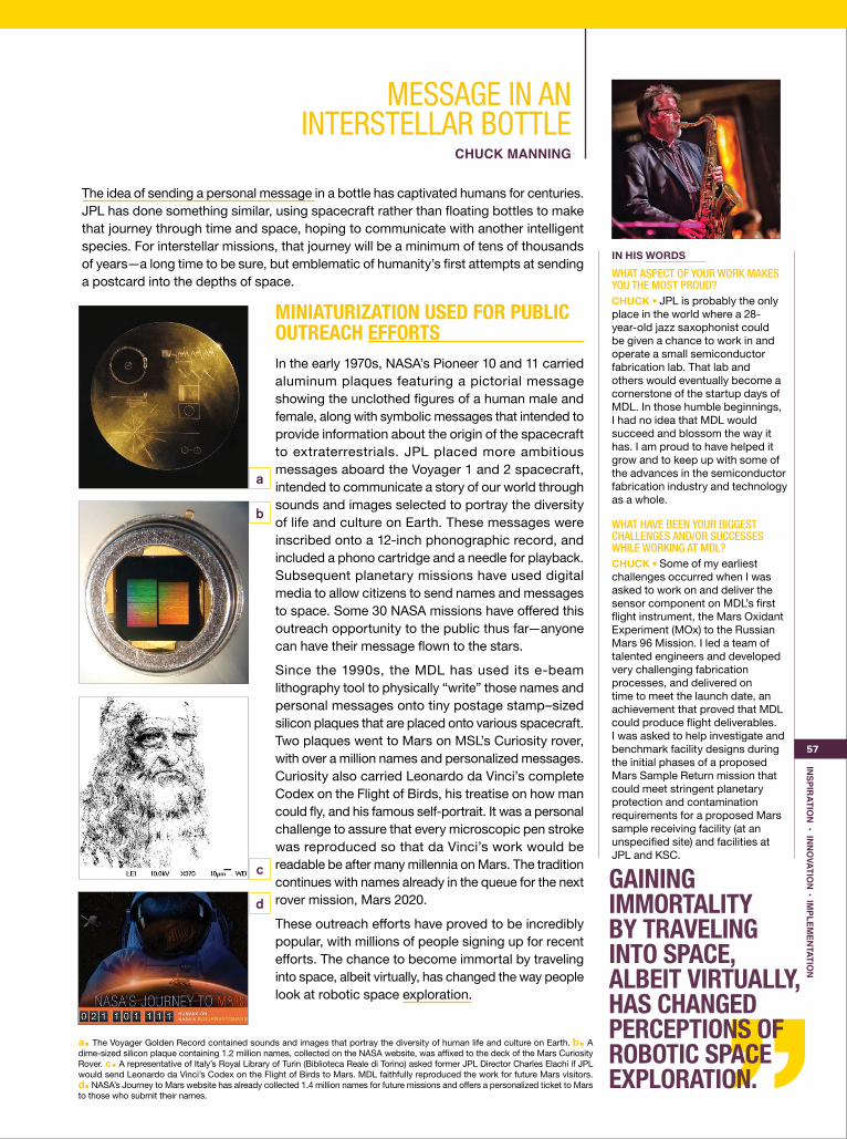
57
INSPIR
ATION
• INN
OVATIO
N • IM
PLEMEN
TATION
a
d
b
c
MESSAGE IN AN INTERSTELLAR BOTTLE
CHUCK MANNING
IN HIS WORDS
WHAT ASPECT OF YOUR WORK MAKES YOU THE MOST PROUD?CHUCK • JPL is probably the only place in the world where a 28- year-old jazz saxophonist could be given a chance to work in and operate a small semiconductor fabrication lab. That lab and others would eventually become a cornerstone of the startup days of MDL. In those humble beginnings, I had no idea that MDL would succeed and blossom the way it has. I am proud to have helped it grow and to keep up with some of the advances in the semiconductor fabrication industry and technology as a whole.
WHAT HAVE BEEN YOUR BIGGEST CHALLENGES AND/OR SUCCESSES WHILE WORKING AT MDL?CHUCK • Some of my earliest challenges occurred when I was asked to work on and deliver the sensor component on MDL’s first flight instrument, the Mars Oxidant Experiment (MOx) to the Russian Mars 96 Mission. I led a team of talented engineers and developed very challenging fabrication processes, and delivered on time to meet the launch date, an achievement that proved that MDL could produce flight deliverables. I was asked to help investigate and benchmark facility designs during the initial phases of a proposed Mars Sample Return mission that could meet stringent planetary protection and contamination requirements for a proposed Mars sample receiving facility (at an unspecified site) and facilities at JPL and KSC.
MINIATURIZATION USED FOR PUBLIC OUTREACH EFFORTS In the early 1970s, NASA’s Pioneer 10 and 11 carried aluminum plaques featuring a pictorial message showing the unclothed figures of a human male and female, along with symbolic messages that intended to provide information about the origin of the spacecraft to extraterrestrials. JPL placed more ambitious messages aboard the Voyager 1 and 2 spacecraft, intended to communicate a story of our world through sounds and images selected to portray the diversity of life and culture on Earth. These messages were inscribed onto a 12-inch phonographic record, and included a phono cartridge and a needle for playback. Subsequent planetary missions have used digital media to allow citizens to send names and messages to space. Some 30 NASA missions have offered this outreach opportunity to the public thus far—anyone can have their message flown to the stars.
Since the 1990s, the MDL has used its e-beam lithography tool to physically “write” those names and personal messages onto tiny postage stamp–sized silicon plaques that are placed onto various spacecraft. Two plaques went to Mars on MSL’s Curiosity rover, with over a million names and personalized messages. Curiosity also carried Leonardo da Vinci’s complete Codex on the Flight of Birds, his treatise on how man could fly, and his famous self-portrait. It was a personal challenge to assure that every microscopic pen stroke was reproduced so that da Vinci’s work would be readable be after many millennia on Mars. The tradition continues with names already in the queue for the next rover mission, Mars 2020.
These outreach efforts have proved to be incredibly popular, with millions of people signing up for recent efforts. The chance to become immortal by traveling into space, albeit virtually, has changed the way people look at robotic space exploration.
GAINING IMMORTALITY BY TRAVELING INTO SPACE, ALBEIT VIRTUALLY, HAS CHANGED PERCEPTIONS OF ROBOTIC SPACE EXPLORATION.
a§ The Voyager Golden Record contained sounds and images that portray the diversity of human life and culture on Earth. b§ A dime-sized silicon plaque containing 1.2 million names, collected on the NASA website, was affixed to the deck of the Mars Curiosity Rover. c§ A representative of Italy’s Royal Library of Turin (Biblioteca Reale di Torino) asked former JPL Director Charles Elachi if JPL would send Leonardo da Vinci’s Codex on the Flight of Birds to Mars. MDL faithfully reproduced the work for future Mars visitors. d§ NASA’s Journey to Mars website has already collected 1.4 million names for future missions and offers a personalized ticket to Mars to those who submit their names.
The idea of sending a personal message in a bottle has captivated humans for centuries. JPL has done something similar, using spacecraft rather than floating bottles to make that journey through time and space, hoping to communicate with another intelligent species. For interstellar missions, that journey will be a minimum of tens of thousands of years—a long time to be sure, but emblematic of humanity’s first attempts at sending a postcard into the depths of space.

JPL
| M
ICR
OD
EVI
CE
S L
AB
OR
ATO
RY
| 20
16-2
017
AN
NU
AL
RE
PO
RT
58
James L. Lamb is the Manager of JPL’s Microdevices Laboratory (MDL); the Technical Group Supervisor for the Central Processing and MDL Support Group; and is a named JPL Principal in Microdevice Engineering and Implementation. He is responsible for all facility, safety, and operational issues associated with this state-of-the-art semiconductor device processing facility. A trained physicist and JPL employee since 1984, James has been associated with MDL operations since its inception.
JPL’s Microdevices Laboratory (MDL) was established to create detectors and other technology advancements to enable breakthrough science for space applications. Three key elements are required to accomplish this mission: 1) Leadership with sustained support, commitment, and vision; 2) Skilled, dedicated, creative, optimistic, and fearless personnel; and 3) Infrastructure and equipment providing the requisite capabilities.
MDL KEY CAPABILITIES The sustained investment in MDL for over 25 years has paid off handsomely. Contributions have been and continue to be accomplished through the creation and delivery of improved sensor technologies across a wide swath of the electromagnetic spectrum from the soft X-ray regime, through the ultraviolet (UV), the visible (VIS), the near-infrared (NIR), the mid-infrared (mid-IR), the far-infrared (far-IR), submillimeter (sub-mm), and millimeter (mm) spectral regions. Innovations have also resulted from technology developments in the areas of characterization instrumentation (e.g., BEEM—ballistic electron emission microscopy), spacecraft control (e.g., microgyro); mini spacecraft propulsion (e.g., MEP–micro electric propulsion); communications (e.g., high-frequency amplifiers and SNSPD–superconducting nanowire single-photon detectors for optical communications); superconducting circuitry (e.g., quantum computers); and in situ instruments for planetary geology (e.g., MOx, Urey, microseismometers); life detection (e.g., microfluidic lab on a chip); and medical applications (e.g., 3-D Marvel endoscope, UV cameras, IR cameras). The MDL infrastructure and capabilities, which have been continually updated and renewed, include a facility constructed to safely handle and monitor acutely hazardous materials including three separate exhaust systems, an RO/DI water plant, certified cleanroom areas down to ISO4 (Class 10), facilities designed and engineered with anti-vibration measures to allow submicron processing, and flexible equipment designs and controls allowing the use of different size and thickness wafers and the use of a variety of materials including Si, GaAs, GaSb, GaN, and superconducting materials. A full suite of semiconductor processing equipment in the areas of patterning, deposition, etching (both F- and Cl- chemistries), and characterization as well as capabilities in the areas of sample preparation and packaging provide end-to-end device fabrication capabilities in the MDL.
Of course, this capability and infrastructure does not happen by itself. Oversight and implementation of MDL’s numerous infrastructure systems, equipment capabilities, and operations have been maintained, renewed, and upgraded by the members of the Central Processing and MDL Support group supported by numerous other organizational elements, all of which allow the continuation of MDL’s cutting-edge capabilities and contributions now and well into the future.
FABRICATING THE FUTURE
JAMES L. LAMB
LEADERSHIP WITH SUSTAINED SUPPORT, COMMITMENT AND VISION; SKILLED, DEDICATED, CREATIVE, OPTIMISTIC, AND FEARLESS PERSONNEL; AND INFRASTRUCTURE AND EQUIPMENT PROVIDING THE REQUISITE CAPABILITIES ARE CRITICAL TO OUR SUCCESS.
below§ Aerial view of JPL’s Microdevices Laboratory (MDL).

a
59
INSPIR
ATION
• INN
OVATIO
N • IM
PLEMEN
TATION
1) E-Beam Lithography. A new JEOL JBX9500FS electron- beam lithography system was procured in 2015, fabricated in 2016, and installed and qualified in 2017. It has enhanced state-of-the-art engineering features with a 3.6nm spot size, large (up to 1000 um) field sizes, reduced spot dwell times (10ns/shot), 100KV & 48KV switchable acceleration voltages, and the ability to write 10 nm features over the entire area of large wafers (up to 9 inches in diameter). Unique enabling techniques developed in JPL’s Microdevices Laboratory over the last 20 years for this system and its predecessors have allowed this capability to not only support the fine patterning required for all technologies developed in MDL, but have pioneered the ability to shape the surface in analog relief patterns (as in gray-scale rather than simple binary patternings), and to do so on curved surfaces with up to 10 mm of curvature. This has enabled the Offner and Dyson form factors for spectroscopy allowing spectrometers to shrink from the size of a small table to the size of a pound cake or even a soda can with improved performance over a wider spectral range. Besides being an enabling technology for the fabrication of improved spectrometer gratings, the system also provides numerous other enabling technologies applicable to planetary science, Mars, astrophysics, Earth science, and supporting the goals of national interest and defense. This includes coronagraph occulting masks (allowing exoplanet imaging and the ability to determine habitability); plasmonic hole arrays and wire-grid polarizers (creating subwavelength-engineered dispersers that can enhance the ability to separate incident wavelengths and eliminate large filters or lenses allowing spectrometers with enhanced throughput and reduced size); metamaterials (key to high-Q structures enabling new instrument architectures such as for submillimeter-wave remote sensing); distributed feedback lasers (a key element for improved smaller uncooled instruments for absorption spectroscopy); and 9”-diameter computed holograms (unavailable anywhere else), and nano optical antennas (enabling a new class of planar optics for optical wavelengths with pattern-definable functionality).
Examples of past enabled instruments and missions: astrophysics: BOOMERANG (Balloon Observations of Millimetric Extra-galactic Radiation and Geophysics); Herschel Space Observatory HIFI; JWST-NIRCam coronography;
planetary: MIRO; Moon Mineralogy Mapper; Mars: CRISM; Mars Science Laboratory (TLS); Earth: Aura Microwave Limb Sounder. Non-NASA: Warfighter; COMPASS; COMPASS AF; HyLITE; HSIT/SPIRITT; ALOHA; MaRS; ARTEMIS; CAO; NEON.
2) Low-Pressure Chemical Vapor Deposition (LPCVD) to Produce Low-Stress (Silicon-Rich) Silicon Nitride Membranes. The Tystar (150 mm / 6-inch wafer diameter) LPCVD has allowed MDL researchers the ability to create silicon and silicon nitride structures of extremely low mass and high strength. Devices on membrane structures increased the sensitivity of the uncooled thermopile detectors for the Mars Climate Sounder (MCS) instrument on the 2005 Mars Reconnaissance Orbiter (MRO), providing the longest unbroken global temperature, dust, and water ice climatology for the atmosphere of Mars (over 10 years). The MDL thermopile arrays on the Diviner Lunar Radiometer Experiment Instrument on the Lunar Reconnaissance Orbiter (LRO) (2009) were used to make the first complete temperature maps of the moon, including the coldest measured surface temperature in the solar system. This was also an enabling capability for the fabrication of the Micromesh Spider-web and polarization sensitive bolometers for the balloon-borne Boomerang telescope (1999), the Herschel Space Observatory (2009), the Planck Observatory (2009), Balloon-borne Large Aperture Submillimeter Telescope (BLAST) (2010–2012), SPIDER balloon-borne experiment (2014), and BICEP 1 (2012), BICEP 2 (2014), and BICEP 3 (2016) deployments in Antarctica. In 1999, these detectors showed for the first time that the universe is “flat,” allowed high-precision photometry and polarization measurements of the cosmic microwave background (CMB) over the entire sky, refining the age of the universe since the Big Bang (13.8 billion years), and constrained measurements of the B-mode signals, an imprint of gravitational waves predicted by the theory of cosmic inflation. Thermopiles for future Europa missions and astrophysics detectors currently being tested in ground-based observations also rely on this capability in MDL. MDL is also building the focal plane module
a§ JEOL JBX 9500 FS electron-beam lithography System: 0.010 μm Res (3.6 nm spot size).
b§ Two views of the TYSTAR LPCVD for 6-inch-diameter wafers with low-stress Si3N4 and atmos. Wet/dry oxidation tubes. b

c
JPL
| M
ICR
OD
EVI
CE
S L
AB
OR
ATO
RY
| 20
16-2
017
AN
NU
AL
RE
PO
RT
60
for the Radiation Budget Instrument (RBI), to be flown on the Joint Polar Satellite System 2 (JPSS-2) mission planned for launch in November 2021. Each pixel relies on thin (100 nm), 1.9-mm-square, suspended, low-stress silicon nitride (LSN) membranes grown by this system.
3) UHV Superconductor Deposition Systems. Ultra high vacuum (UHV) sputtering systems from Lesker and AJA have allowed the growth of high-transition temperature niobium nitride (NbN) superconductor coatings by reactive sputtering and tungsten silicide (WSi2) coatings. These coatings have been critical for the development and delivery of sensitive superconductor-insulator-superconductor (SIS) detectors for heterodyne mixers, microwave kinetic-inductance detectors (MKIDs), superconducting nanowire single-photon detectors (SNSPDs), and transition-edge sensors (TESs) for sub-millimeter-wave astronomy and optical communications. The ultra high vacuum is required to avoid contamination of the coatings during growth, which relies on specific recipes developed by the expert resident staff over the last 30 years.
This capability provided enabling high-frequency detectors for the Spectral and Photometric Imaging Receiver (SPIRE) instrument and the Heterodyne Instrument for the Far-Infrared (HIFI) on the Herschel Space Observatory. They detected water vapor on Ceres and in a torus around Enceladus, as well as around a nearby star; established that the water from comet Hartley 2 had the same isotopic composition as the water on Earth; discovered many new molecules and new terahertz spectral lines from molecules in interstellar space; and provided large-area sky maps detecting distant infrared luminous galaxies. High-frequency detectors provided to Planck allowed mapping of millimeter- and sub-millimeter wave emissions from interstellar dust and carbon monoxide (CO) over the entire sky, providing crucial information about the formation of galaxies and the geometry of the universe. The SNSPD array established an optical communication link from Table Mountain, CA, with the LADEE satellite orbiting the moon (2012). The microwave kinetic-inductance detector (MKID) first demonstrated in 2000 has been widely adopted worldwide
for ground-based millimeter/sub-milliter astronomy. MDL-fabricated 484-element MKID arrays are baselined for the sub-millimeter photometry array called MAKO at the Caltech Submillimeter Observatory (CSO) — first light in 2012). MKIDS are also used for energy-resolved photon detection at optical, UV, and X-ray wavelengths.
4) Large-Format Flip-Chip Aligner Bump Bonding Capabilities. Flip-chip bonding involves detectors (usually focal plane arrays [FPAs]), which are “flipped,” aligned, and mated to silicon readout integrated circuits (ROICs) via cold or heated-welds of clean indium bumps on each pixel to form single devices. MDL has three indium evaporators to form the bumps and has developed techniques to ensure the bumps do not oxidize. Prior art involved bump bonding of only small single-chip devices since the alignment precision and forces invloved increase geometrically with size. However, next-generation FPAs required by NASA are large-format monolithic FPAs, equal to or greater than 2Kx2K arrays. A large monolithic FPA can reduce overall system cost by eliminating cryocooler needs, increasing spatial resolution, and reducing the power budget. MDL has invested in an SET FC300 Flip Chip Bump Bonder that allows the alignment and bonding of full wafers (up to 300 mm = 12 inches in diameter) and large-format monolithic FPAs enabling JPL and MDL to meet the needs of future NASA missions. There are only a handful of such systems in the United States with this enabling capability.
This relatively unique capability has been used to develop 16-megapixel IR focal planes to meet the needs of the US Army and National Reconnaissance Office’s (NRO’s) persistence surveillance efforts. It was also utilized to develop and deliver a 7.5-/12-µm dual-broadband megapixel quantum-well infrared photodetector (QWIP) focal plane array to the Hyperspectral Thermal Emission Spectrometer (HyTES) airborne spectral imager in 2012. The HyTES instrument is the trailblazer for the Hyperspectral Infrared Imager (HyspIRI) mission proposed in the NASA Earth science decadal survey, and also recommended by the National Research Council Decadal Survey requested by NASA, NOAA, and USGS.
Eventually, HyspIRI needs even larger FPAs to reduce the global revisit time (the current NASA CO2 measuring instrument AIRS takes approximately 8 days for global revisit). These data will be used for a wide variety of studies, primarily regarding the carbon cycle, ecosystem, and Earth surface and interior focus areas.
Development of the potentially revolutionary barrier infrared detectors (BIRDs), complementary barrier infrared detectors (C-BIRDs), and high operating temperature barrier infrafed detectors (HOT BIRDs) have also been aided by this capability. The NASA 6U CubeSat Infrared Atmospheric Sounder (CIRAS) is based on JPL-developed MWIR HOT BIRD focal plane technology.
Additionally, the recently proposed Imaging Spectroscopic Telescope for Origins Surveys (MIDEX–ISTOS) requires large- area delta-doped charge-coupled device (CCD) arrays. NASA mission proposals that have 4Kx4K large-format FPAs that are in the astrophysics/cosmology area are MIDEX-ORION, MIDEX-ISTOS, JDEM, LSST, Palomar Tech Demo, and
c§ One of two Lesker UHV sputtering systems for superconducting materials.

d
e
61
INSPIR
ATION
• INN
OVATIO
N • IM
PLEMEN
TATION
Sub-orbital FIREBALL. NASA mission proposals with large-format FPAs that are in the planetary area are Mars 2020 and Europa. This can be an enabling capability for all JPL missions requiring the bump bonding of large-format imagers.
5) III-V Sb Molecular-Beam Epitaxy for Long- Wave-length IR FPAs. The creation of barrier infrared detectors (BIRDs) that offer improved higher temperature performance at lower costs for the near-infrared (NIR; 0.75–1.4 µm), short wavelength infrared (SWIR; 1.4–3 µm), mid-wavelength infrared (MWIR, 3–5 µm), and long-wavelength infrared (LWIR; 5–15 µm) has been enabled by the ability to grow antimonide-based Type-II superlattice structures on GaSb substrates using a Veeco Gen-3 molecular-beam epitaxy (MBE) machine in the MDL. These structures have great potential in realizing high-performance, large-format, highly uniform infrared focal plane arrays at lower cost. The availability of large-area, epi-ready GaSb substrates, along with relatively easy III-V materials growth and processing technology compared to its II-VI (i.e., HgCdTe) counterpart, make this possible. Development of the potentially revolutionary BIRDs, complementary barrier infrared detectors (C-BIRDs), and high operating temperature barrier infrared detectors (HOT BIRDs) has been enabled by this capability. These antimonides superlattice-based detectors can operate at an elevated temperature of 150 K with suppressed material defects and surface-related dark current, while yielding nearly 100% quantum efficiency in the mid-wavelength infrared (MWIR; 3–5 µm), the short-wave infrared (SWIR; 1.4–3 µm), and the near-infrared (NIR; 0.75–1.4 µm). A novel device architecture invented in MDL has also increased the long-wavelength infrared (LWIR 5–15 µm) from 30% (due to insufficient diffusion length) to ~80%. The NASA 6U CubeSat Infrared Atmospheric Sounder (CIRAS) is based on JPL-developed MWIR HOT BIRD focal plane technology.
6) 200-mm (8-inch) Silicon Molecular-Beam Epitaxy (MBE) System for Delta-Doped UV Detectors and Doped Superlattice Detectors. This Veeco GEN200 Silicon MBE allows the manipulation of the electronic bandgap structure of silicon imagers. Delta-doping is a technique that first relies on precision thinning of prefabricated silicon imagers for backside illumination. Next a buried charge layer of epitaxially grown, heavily doped silicon is deposited. This layer is only a single atomic layer thick (and results in the name of delta-doping). Finally, the delta-doped layer is overcoated
by epitaxially grown silicon to place it at the right depth. This process provides for the elimination of trapped charge states on the surface to make the devices sensitive in the ultraviolet (UV) and soft X-ray regime with extreme sensitivity; so much so that it is capable of detecting even single photons. It may also be described as two-dimensional doping for surface passivation. These processes have been demonstrated on a variety of silicon-based formats, and have resulted in 100% internal quantum efficiency (QE) throughout the UV–visible wavelength ranges with record-breaking stability against potentially damaging radiation. The technology has been demonstrated in ground-based observatories (Palomar and Mount Bigelow), balloon experiments (FIREBall-2), sounding rockets (LIDOS, MICA, CHESS), and has been proposed for several satellite missions (the Large Ultraviolet Optical IR Surveyor Mission (LUVOIR) and the Habitable Exoplanet imager (HabEx), which would require unprecedented large apertures, high throughput, and wide spectral range, all of which can be provided by this MDL capability. These detectors can be used to study the formation of young stars. It may also be applied as detectors in UV lithography systems in the semiconductor industry providing enhanced longevity and sensitivity.
The doped-superlattice detectors provide the means of achieving high efficiency and fast response on avalanche photodiodes with record-breaking stability against potentially damaging radiation. It has been applied to gamma-ray scintillator technology with subnanosecond temporal resolution and has shown the ability to withstand unprecedented rates and doses of high-energy gamma radiation. When integrated with solar-blind antireflection coatings the doped-superlattice detectors are applicable to NASA applications such as X-ray pulsar navigation, time-gated Raman spectroscopy, and planetary gamma-ray spectrometers.
d § SET FC-300 Flip-Chip Bump Bonder.
e§ Veeco Epi GEN III Sb MBE.

if,g§ Two views of Veeco GEN200 (8-inch) Si MBE. h§ Oxford OpAL ALD system.
i§ Beneq TFS-200 ALD system.JPL
| M
ICR
OD
EVI
CE
S L
AB
OR
ATO
RY
| 20
16-2
017
AN
NU
AL
RE
PO
RT
62
7) Atomic Layer Deposition (ALD) Capabilities. MDL has invested in an Oxford Plasmalab 80 OpAL atomic layer deposition (ALD) system with radical enhanced upgrade and a Beneq TFS-200 ALD system. These tools, coupled with an expert processing staff in this technology area, enable the conformal deposition of metals and dielectrics, atomic layer by atomic layer, in a relatively low-temperature process (nominally 300 degrees C), that allows easy precision coating scalability to larger wafer diameters and even complex structures. Of particular note is the application of this capability to the growth of precision dielectric anti-reflection (AR) coatings to UV detectors, improving the coupling efficiency of UV light to the detectors, and in some instances improving quantum efficiencies from 6% to 60%. There is also development work going on that offers the promise of depositing both thin MgB2 superconducting films over large wafer areas and controlled dielectric growths for numerous detector designs for astrophysics. It has further been utilized to produce TiN protective films to minimize and eliminate forward contamination for the Mars 2020 sample return sample acquisition drill bits, to fabricate ALD Al2O3 passivating films for III-V detectors, and to deposit a titanium getter film for the first InSight mission seismometer package domes.
JPL’S MICRODEVICES LABORATORY (MDL) WAS ESTABLISHED TO CREATE DETECTORS AND OTHER TECHNOLOGY ADVANCEMENTS TO ENABLE BREAKTHROUGH SCIENCE FOR SPACE APPLICATIONS.8) Load-Locked Thermal Co-Evaporator Capability for Broadband IR Bolometer Depositions. Precision co-evaporation of exotic materials has been enabled by a custom designed AJA load-locked evaporator. These depositions may be designed to create extremely sensitive thermopile arrays, particularly when they are deposited onto MDL LPCVD grown thin low-stress silicon nitride membranes, enhanced by black silicon optical absorbers produced by cryo-etching. Thermopiles are essentially enhanced thermocouples. As such they are low-power, broadband, insensitive to temperature drift, and extremely radiation-tolerant. This, coupled with the fact that thermopiles require no cryocooler or bias circuit, make them ideally suited for space and deep-space applications. Thermopile arrays from MDL are flying on JPL’s Mars Climate Sounder instrument on the Mars Reconnaissance Orbiter (2005 to present), on the Diviner Lunar Radiometer Experiment instrument (2009), and are under development for the Diviner–Europa (Diviner-E) instrument, a multispectral infrared imaging radiometer for planned Europa missions (in the 2020s).
9) Deep Trench Reactive Ion Etching (DRIE) and Deep Silicon Etching (DSE) Capabilities. These capabilities (an STS deep trench reactive ion etching system with SOI upgrade, and a PlasmaTherm Versaline deep silicon etcher) allow the creation of deep channels and other structures in silicon, enabling the use of the third (z-axis) dimension. Traditional semiconductor processing allows aspect ratios of about 1:10 (i.e., 1 wide and 10 deep). The DRIE and DSE capability expands this to 1:40 and even more. This was a key capability in creating the micromesh spider bolometers antenna structure to measure temperature fluctuations in the cosmic microwave background. It has also been a key capability for microgyro and microseismometer applications, and holds the promise of allowing the creation of precision nozzle arrays with wicking channels for micro electric propulsion (MEP) designs, an attitude control and propulsion technology for CubeSats and U-Sats, as well as enabling the creation of through-wafer vias for numerous applications.
f
g
h

63
INSPIR
ATION
• INN
OVATIO
N • IM
PLEMEN
TATION
MATERIAL DEPOSITION ● Thermal Evaporators (5)
● Electron-Beam Evaporators (7)
● Angstrom Engineering Indium-metal Evaporator
● Ultra-High-Vacuum (UHV) Sputtering Systems for Dielectrics and Metals (3)
● Ultra-High-Vacuum (UHV) Sputtering Systems for Superconducting Materials (3)
● AJA Load Locked Thermal Co-Evaporator for Broadband IR Bolometer Depositions
● PlasmaTherm 790 Plasma Enhanced Chemical Vapor Deposition (PECVD) for Dielectrics with Cortex Software Upgrade
● Oxford Plasmalab System 100 Advanced Inductively Coupled Plasma (ICP) 380 High-Density Plasma Enhanced Chemical Vapor Deposition (HD PECVD) System for Low Temperature Dielectric Growths
● Oxford Plasmalab 80 OpAL Atomic Layer Deposition (ALD) System with Radical Enhanced Upgrade
● Beneq TFS-200 Atomic Layer Deposition (ALD) System with Meaglow Plasma Source Upgrade
● Tystar (150mm /6-inch) Low-Pressure Chemical Vapor Deposition (LPCVD) with 2 Tubes for
♦Low Stress Silicon Nitride
♦Atmospheric Wet/Dry Oxidation ● Carbon Nanotube Furnace Systems (2)
● Electroplating Capabilities
♦Molecular-Beam Epitaxy (MBE) ● Veeco GEN200 (200mm/8-inch) Si MBE for UV CCD Delta Doping (Silicon)
♦Veeco Epi GEN III MBE (Antimonide Materials)
♦Riber MBE for UV CCD Delta Doping (Silicon)
♦Riber Device MBE (GaAs)
LITHOGRAPHIC PATTERNING ● Electron-Beam (E-beam) Lithography: JEOL JBX 9500FS E-beam lithography system with a 3.6 nm spot size, switchable 100,000 & 48,000 volt acceleration voltages, ability to handle wafers up to 9 inches in diameter, and hardware and software modifications to deal with curved substrates having up to 10 mm of sag
● GCA Mann Wafer Stepper with custom stage allowing different sizes and thicknesses of wafers (0.7-µm resolution)
● Canon FPA3000 i4 i-Line Stepper (0.35-µm resolution)
● Canon FPA3000 EX3 Stepper with EX4 Optics (0.25-µm resolution)
● Canon FPA3000 EX6 DUV Stepper (0.15-µm resolution)
● Contact Aligners:
♦Karl Suss MJB3
♦Karl Suss MJB3 with backside IR
♦ Suss MA-6 (UV300) with MO Exposure Optics upgrade
♦ Suss BA-6 (UV400) with jigging supporting Suss bonder
● Wafer Track/Resist/Developer Dispense Systems:
♦Suss Gamma 4 Module Cluster System
♦Site Services Spin Developer System
♦ SolarSemi MC204 Microcluster Spin Coating System with Hot Plate & Dispense Upgrades
● Yield Engineering System (YES) Reversal Oven
● Ovens, Hotplates, furnaces, and Manual Spinners (including 2 Solitec 5110C spinners, and a Suss RC8 Spin Coater)
DRY ETCHING ● Commonwealth IBE-80 Ion Mill
● Branson Plasma Ashers (2)
● Tepla PP300SA Microwave Plasma Asher
FLUORINE-BASED PLASMA ETCHING SYSTEMS ● STS Deep Trench Reactive Ion Etcher (DRIE) with SOI Upgrade
● PlasmaTherm Versaline Deep Silicon Etcher (DSE/DRIE)
● Unaxis Shuttleline Load-Locked Fluorine Inductively Coupled Plasma (ICP) RIE
● PlasmaTherm APEX SLR Fluorine-based ICP RIE with Laser End Point Detector
● Plasmaster RME-1200 Fluorine RIE
● Plasma Tech Fluorine RIE
● STJ RIE for Superconductors
● Custom XeF2 etcher
CHLORINE-BASED PLASMA ETCHING SYSTEMS ● Unaxis Shuttleline Load-Locked Chlorine Inductively Coupled Plasma (ICP) RIE
● PlasmaTherm Versaline Chlorine-based ICP Etcher
WET ETCHING & SAMPLE PREPARATION ● RCA Acid Wet Bench for 6-inch Wafers
● Solvent Wet Processing Benches (7)
● Rinser/Dryers for Wafers including Semitool 870S Dual Spin Rinser Dryer
● Chemical Hoods (7)
● Acid Wet Processing Benches (8)
● Tousimis 915B Critical Point Dryer
● Rapid Thermal Processors/Contact Alloyers (2)
● Polishing and Planarization Stations (5)
● Strasbaugh 6EC Chemical Mechanical Polisher
● Precitech Nanonform 250 Ultra Diamond Point Turning System
APPENDICES | MDL EQUIPMENT COMPLEMENT

JPL
| M
ICR
OD
EVI
CE
S L
AB
OR
ATO
RY
| 20
16-2
017
AN
NU
AL
RE
PO
RT
64
● SET North America Ontos 7 Native Oxide (Indium Oxide) Removal Tool with Upgrade
● Novascan UV8 Ultraviolet Light Ozone Cleaner
● New Wave Research EzLaze 3 Laser Cutting System
● Indonus HF VPE-150 Hydrofluoric Acid Vapor Phase Etcher
● Laurell Technologies EDC 650 Dilute HF/Ozonated DI Water Spin Cleaning System with MKS Instruments Liquizon Ozonated Water Generator System
● Osiris Fixxo M200 TT Wafer Mounting Tool
● Surfx Atomflo 500 Argon Atmospheric Plasma Surface Activation System for wafer bonding
PACKAGING ● SET FC-300 Flip Chip Bump Bonder
● Karl Suss Wafer Bonder
● Electronic Visions AB1 Wafer Bonder
● EVG 520Is Semi-Automatic Wafer Bonding System
● Finetech Fineplacer 96 “Lambda” Bump Bonder
● Thinning Station and Inspection Systems for CCD Thinning
● Wire Bonding
● DISCO 320 and 321 Wafer Dicers (2)
● Tempress Scriber
● Pick and Place Blue Tape Dispenser System
● Loomis LSD-100 Scriber Breaker
● SCS Labcoater 2 (PDS 2010) Parylene Coating System
CHARACTERIZATION ● Profilometers (2) (Dektak 8 & Alphastep 500)
● Frontier Semiconductor FSM 128 Film Stress Measuring system
● Frontier Semiconductor FSM 128-NT (200mm/8-inch) Film Stress and Wafer Bow Mapping System
● LEI 1510 Contactless Sheet Resistance Tool
● FISBA μPhase 2 HR Compact Optical Interferometer
● Senetech SE 850 Multispectral Ellipsometer
● Horiba UVSEL 2 (190-2100 nm) Ellipsometer
● Filmetrics F20-UV (190-1100 nm) Thin Film Spectrometer Measurement System
● Filmetrics F40-UVX (190-1700 nm) Thin Film Spectrometer Measurement System with Microscope
● Dimension 5000 Atomic Force Microscope (AFM)
● Park Systems Inc. NX20 Atomic Force Microscope (AFM)
● KLA-Tencor Surfscan 6220 Wafer Particle Monitor
● JEOL JSM-6700 Field Emission SEM with EDX
● Nikon & Zeiss Inspection Microscopes with Image Capture (3)
● Keyence VHX-5000 Digital Microscope
● McBain BT-IR Z-Scope IR Microscope Workstation
● Olympus LEXT 3D Confocal Microscope
● Mitaka NH-5Ns 3D Profiler
● Electrical Probe Stations (4) with Parameter Analyzers (2)
● RPM2035 Photoluminescence Mapping System
● Fourier Transform Infrared (FTIR) Spectrometers (3) including Bruker Optics Vertex 80 FTIR
● PANalytical X’Pert Pro MRD with DHS High Temperature Stage X-ray Diffraction System
● Surface Science SSX501 XPS with Thermal Stage
● Custom Ballistic Electron Emission Microscopy (BEEM) System
● Custom UHV Scanning Tunneling Microscope (STM)
● Nanometrics ECV Pro Profiler
● VEECO / WYKO NT 9300 Surface Profiler (including 50X optics)
● Zygo ZeMapper non-contact 3D Profiler
● Thermo Scientific LCQ Fleet CE / MS (Capillary Electrophoresis / Mass Spectrometer) System
above§ Much of MDL’s PlasmaThermVersaline Deep Silicon Etcher (DSE) is located in the chase adjacent to the cleanroom processing area where samples are loaded.

JOURNAL PUBLICATIONS
65
INSPIR
ATION
• INN
OVATIO
N • IM
PLEMEN
TATION
JOURNAL PUBLICATIONS1. N. Acharya, M. A. Wolak, T. Tan, N. Lee, A. C. Lang,
M. Taheri, D. Cunnane, B. S. Karasik, and X. X. Xi, “MgB2 Ultrathin Films Fabricated by Hybrid Physical Chemical Deposition and Ion Milling,” APL Mater., 4, 086114, 2016.
2. T. Kiuru, G. Chattopadhyay, T. J. Reck, A. J. Minnich, R. Lin, E. Schlecht, J. V. Siles, C. Lee, and I. Mehdi, “ Thermal Characterization of Substrate Options for High-Power THz Multipliers Over a Broad Temperature Range,” IEEE Trans. Terahertz Sci. Technol., 6 (2), 328, 2016.
3. T. Reck, C. Jung-Kubiak, and G. Chattopadhyay, “A 700 GHz MEMS Waveguide Switch,” IEEE Trans. Terahertz Sci. Technol., 6 (4), 641, 2016.
4. C. Jung-Kubiak, T. Reck, J. Siles, R. Lin, J. Gill, C. Lee, K. Cooper, I. Mehdi, and G. Chattopadhyay, “A Multi-Step DRIE Process for Complex Terahertz Waveguide Components,” IEEE Trans. Terahertz Sci. Technol., 6 (5), 690, 2016.
5. U. Shah, E. Decrossas, C. Jung-Kubiak, T. Reck, G. Chattopadhyay, I. Mehdi and J. Oberhammer, “Submillimeter-Wave 3.3-bit RF MEMS Phase Shifter Integrated in Micromachined Waveguide,” IEEE Trans. Terahertz Sci. Technol., 6 (5), 706, 2016.
6. A.Tang, T. Reck, and G. Chattopadhyay, “CMOS System-on-Chip Techniques in Millimeter-Wave/THz Instruments and Communications for Planetary Explorations,” IEEE Commun. Mag., 54 (10), 176, 2016.
7. S. Nikzad, M. Hoenk, M., A. D. Jewell, J. Hennessy, A. G. Carver, T. J. Jones, T. M. Goodsall, E. T. Hamden, P. Suvarna, J. Bulmer, J. and F. Shahedipour-Sandvik, E. Charbon, P. Padmanabhan, B. Hancock and L. D. Bell, “Single Photon Counting UV Solar-Blind Detectors Using Silicon and III-Nitride Materials,” Sensors, 16 (6), 927, 2016.
8. J. Hennessy, K. Balasubramanian, C. S. Moore, A. D. Jewell, S. Nikzad, K. France, and M. Quijada, “Performance and Prospects of Far Ultraviolet Aluminum Mirrors Protected by Atomic Layer Deposition,” J. Astron. Telesc. Instrum. Syst., 2 (4), 041206, 2016.
9. D. Hitlin, J. H. Kim, J. Trevor, J. Hennessy, M. Hoenk, A. Jewell, R. Farrell, R. and M. McClish, “An APD for the Detection of the Fast Scintillation Component of BaF2,” IEEE Transactions on Nuclear Science, 63 (2), pp. 513-515, 2016.
10. E. T. Hamden, A. D. Jewell, C. A. Shapiro, S. R. Cheng, T. M. Goodsall, J. Hennessy, M. Hoenk; T. Jones, S. Gordon, H. R. Ong, D. Schiminovich, D. C. Martin, and S. Nikzad, “Charge-Coupled Devices Detectors with High Quantum Efficiency at UV Wavelengths,” J. Astron. Telesc. Instrum. Syst., 2 (3), 036003, 2016.
11. J. Hennessy, A. D. Jewell, K. Balasubramanian, and S. Nikzad, “Ultraviolet Optical Properties of Aluminum Fluoride Thin Films Deposited by Atomic Layer Deposition,” J. Vac. Sci. Technol. A, 34, 01A120, 2016.
12. A. Plazas, C. Shapiro, A. Kannawadi, R. Mandelbaum, J. Rhodes, and R. Smith, “The Dffect of Detector Non-linearity on WFIRST PSF Profiles for Weak Gravitational Lensing Measurements,’’ PASP, arXiv:1605.01001, 2016.
13. J. Correa, C. B. Wunderer, A. Marras, A. Allahgholi, A. Gloskovskii, P. Göttlichera, S. Lange, S. Reza, I. Shevyakov, M. Tennert, M. Niemann, H. Hirsemann, S. Smoljanin, J. Supra, Q. Xia, M. Zimmer, J. Viefhaus, F. Scholz, J. Seltmann, S. Klumpp, N. Guerrini, B. Marsh, I. Sedgwick, T. Nicholls, R. Turchetta, G. Cautero, D. Giuressi, A. Khromova, R. Menk, G. Pinaroli, L. Stebel, N. Zema, S. Rinaldi, D. Catone, U. Pedersen, N. Tartoni, H. J. Hyun, K. S. Kim, S. Y. Rah, M. E. Hoenk, A. D. Jewell, T. J. Jones, S. Nikzad, and H. Graafsmaa, “On the Charge Collection Efficiency of the PERCIVAL Detector,” JINST 11 C12032, doi:10.1088/1748-0221/11/12/C12032, 2016.
14. A. Khromova, G. Cautero, D. Giuressi, R. Menk, G. Pinaroli, L. Stebel, J. Correa, A. Marras, C. B. Wunderer, S. Lange, M. Tennert, M. Niemann, H. Hirsemann, S. Smoljanin, S. Reza, H. Graafsma, P. Göttlicher, I. Shevyakov, J. Supra, Q. Xia, M. Zimmer, N. Guerrini, B. Marsh, I. Sedgwick, T. Nicholls, R. Turchetta, U. Pedersen, N. Tartoni, H. J. Hyun, K. S. Kim, S. Y. Rah, M. E. Hoenk, A. D. Jewell, T. J. Jones, and S. Nikzad, “Report on Recent Results of the PERCIVAL Soft X-Ray Imager,” Journal of Instrumentation, 11: C11020–C11020, 2016.
15. K. Kannawadi, C. Shapiro, R. Mandelbaum, C. Hirata, J. Kruk, and J. Rhodes, “The Impact of Interpixel Capacitance in CMOS Detectors on PSF Shapes and Implications for WFIRST,’’ PASP, 128, 095001, arXiv:1512.01570 (2016).
16. S. Nikzad et al., “Brain Mapping and Therapeutics,” Special Issue Guest Editorial, Neurophotonics, 4 (1), 011001. doi:10.1117/1.NPh.4.1.011001, Apr 3, 2017.
17. S. Nikzad, “Space Technology and Medicine: Space Technologies Find Their Place in Healthcare Applications,” SPIE Professional Magazine, DOI: 10.1117/2.4201704.17, April 2017.
18. S. Nikzad, A. D. Jewell, M. E. Hoenk, T. J. Jones, J. Hennessy, T. Goodsall, A. Carver, C. Shapiro, S. R. Cheng, E. Hamden, G. Kyne, D. C. Martin, D. Schiminovich, P. Scowen, K. France, S. McCandliss, and R. E. Lupu, “High Efficiency UV/Optical/NIR Detectors for Large Aperture Telescopes and UV Explorer Missions,” JATIS, arXiv:1612.04734v2 [astro-ph.IM], 2016.
19. K. Hossain, L. Hoglund, L. C. Phinney, T. D. Golding, G. Wicks, A. A. Khoshakhlagh, D. Ting, A. Soibel, and S. Gunapala, “Hydrogenation Defect Passivation for Improved Minority Carrier,” J. of Electronics Materials, DOI: 10.1007/s11664-016-4617-z, 2016.
20. D. Z. Ting, A. Soibel, L. Höglund, C. J. Hill, S. A. Keo, A. Fisher, and S. D. Gunapala, “High-Temperature Characteristics of an InAsSb/AlAsSb n+Bn Detector,” J. Electronics Materials, 45 (9), p. 4680, DOI: 10.1007/s11664-016-4633-z, 2016.
21. L. Höglund, D. Z. Ting, A. Khoshakhlagh, A. Soibel, A. Fisher, C. J. Hill, S. Keo, S. Rafol, and S. D. Gunapala, “Influence of Proton Radiation on the Minority Carrier Lifetime in Midwave Infrared InAs/InAsSb Superlattices,” Applied Physics Letters, 108, 263504, 2016.

JPL
| M
ICR
OD
EVI
CE
S L
AB
OR
ATO
RY
| 20
16-2
017
AN
NU
AL
RE
PO
RT
66
22. D. Ting, A. Soibel, and S. Gunapala, “Hole Effective Masses and Subband Splitting in Type-II Superlattice Infrared Detectors,” Appl. Phys. Lett., 108, 183504; doi: 10.1063/1.4948387, 2016.
23. A. Soibel, D. Z. Ting, C. J. Hill, A. M. Fisher, L. Hoglund, S. A. Keo , and S. D. Gunapala, “Mid-Wavelength Infrared InAsSb/InSb nBn Detector with Extended Cut-Off Wavelength,” Applied Physics Letters, 109, 103505; doi: 10.1063/1.4962271, 2016.
24. D. Weeraddana, M. Premaratne, S. D. Gunapala, and D. L. Andrews, “Quantum Electrodynamical Theory of High-Efficiency Excitation Energy Transfer in Laser-Driven Nanostructure Systems,” Physical Review B – Condensed Matter and Materials Physics, 94 (8), art. no. 085133, 2016.
25. C. Jayasekara, M. Premaratne, S. D. Gunapala, and M. I. Stockman, “MoS2 Spaser,” Journal of Applied Physics, 119 (13), art. no. 133101, 2016.
26. C. S. Kumarasinghe, M. Premaratne, S. D. Gunapala, and G. P. Agrawal, “Design of All-Optical, Hot-Electron Current-Direction-Switching Device Based on Geometrical Asymmetry,” Scientific Reports, 6, art. no. 21470, 2016.
27. C. S. Kumarasinghe, M. Premaratne, S. D. Gunapala, and G. P. Agrawal, “Theoretical Analysis of Hot Electron Injection from Metallic Nanotubes into a Semiconductor Interface,” Physical Chemistry Chemical Physics, 18 (27), pp. 18227–18236, 2016.
28. X.-Y. Zhou, D. Lummerzheim, R. Gladstone, S. B. Rafol, S. Gunapala, Y.-T. He, and D. Hampton, “Development of a Near-Infrared Balloon-Borne Camera for Dayside and Sunlit Auroral Observations,” J. Geophys. Res. Space Physics, 122, doi:10.1002/ 2016JA023317, 2017.
29. S. Mallawaarachchi, M. Premaratne, S. D. Gunapala, and P. K. Maini, “Tuneable Superradiant Thermal Emitter Assembly,” J. Physical Review B, DOI: 10.1103/PhysRevB, 95.155443, 2017.
30. A. Khoshakhlagh and S. D. Gunapala, “Band Engineering, Growth and Characteristics of Type-II InAs/GaSb Superlattice- Based Detectors,” Neurophoton, 4 (1), 011014, 2017.
31. B. Kern, O. Guyon, R. Belikov, D. Wilson, R. Muller, E. Sidick, B. Balasubramanian, J. Krist, I. Poberezhskiy, and H. Tang, “Phase-Induced Amplitude Apodization Complex Mask Coronagraph Mask Fabrication, Characterization, and Modeling for WFIRST-AFTA,” J. Astron. Telesc. Instruments, Syst., 2 (1), 11014, 2016.
32. B.-J. Seo, B. Gordon, B. Kern, A. Kuhnert, D. Moody, R. Muller, I. Poberezhskiy, J. Trauger, and D. Wilson, “Hybrid Lyot Coronagraph for Wide-Field Infrared Survey Telescope—Astrophysics Focused Telescope Assets: Occulter Fabrication and High Contrast Narrowband Testbed Demonstration,” J. Astron. Telesc. Instruments, Syst., 2 (1), 11019, 2016.
33. P. Mouroulis, R. O. Green, B. Van Gorp, L. B. Moore, D. W. Wilson, and H. A. Bender, “Landsat Swath Imaging Spectrometer Design,” Opt. Eng., 55 (1), 15104, 2016.
34. P. Mouroulis, R. O. Green, B. Van Gorp, L. B. Moore, D. W. Wilson, and H. A. Bender. “Landsat Swath Imaging Spectrometer Design,” Optical Engineering, 55, No. 1, 015104–015104, 2016.
35. F. Shi, K. Balasubramanian, R. Hein, R. Lam, D. Moore, J. Moore, K. Patterson, I. Poberezhskiy, J. Shields, E. Sidick, H. Tang, T. Truong, J. K. Wallace, X. Wang, and D. Wilson, “Low-Order Wavefront Sensing and Control for WFIRST-AFTA Coronagraph,” J. Astron. Telesc. Instruments, Syst., 2 (1), 11021, 2016.
36. V. J. Scott, H. Manohara, R. Toda, L. Del Castillo, R. Murthy, J. Mulder, E. Murty, and M. C. Thompson, “Robust CNT Field Emitters: Patterning, Growth, Transfer, and In Situ Anchoring,” Nanotechnology, 27, 494002, 2016.
37. R. M. Briggs, C. Frez, M. Fradet, S. Forouhar, R. Blanchard, L. Diehl, and C. Pflügl, “Low-Dissipation 7.4-μm Single-Mode Quantum Cascade Lasers Without Epitaxial Regrowth,” Optics Express, 24, 14589–14595, 2016.
38. J. S. Creamer, M. F. Mora, and P.A. Willis, “Enhanced Resolution of Chiral Amino Acids with Capillary Electrophoresis for Biosignature Detection in Extraterrestrial Samples,” Anal. Chem., 89, 1329, 2017.
39. H. Zhu and M. Rais-Zadeh, “Non-Reciprocal Acoustic Transmission in a GaN Delay Line Using the Acoustoelectric Effect,” J. IEEE Electron Device Lett., 38 (6) 802, 2016.
40. P. Szypryt, B. A. Mazin, G. Ulbricht, B. Bumble, S. R. Meeker, C. Bockstiegel, and A. B. Walter, “High Quality Factor Platinum Silicide Microwave Kinetic Inductance Detectors,” Applied Physics Letters, 109, 151102, 2016.
41. P.A.R. Ade, J. J. Bock, K. G. Megerian, A. D. Turner, A. C. Weber, et al., “Improved Constraints on Cosmology and Foregrounds from BICEP2 and Keck Array Cosmic Microwave Background Data with Inclusion of 95 GHz Band,” Physical Review Letters, 116 (3), 031302, 2016.
42. P.A.R. Ade, J. J. Bock, K. G. Megerian, A. D. Turner, A. C. Weber, et al., “Bicep2/Keck Array VIII: Measurement of Gravitational Lensing From Large-Scale B-Mode Polarization,” The Astrophysical Journal, 833(2), 228, 2016.
43. W.L.K. Wu, P.A.R Ade, J. J. Bock, K. G. Megerian, A. D. Turner, A. C. Weber, et al., “Initial Performance of Bicep3,” Journal of Low Temperature Physics, 184.3-4, pp. 765–771, 2016.
44. P.A.R. Ade, J. J. Bock, K. G. Megerian, A. D. Turner, A. C. Weber, et al., “BICEP2/Keck Array. VII. Matrix Based E/B Separation Applied to Bicep2 and the Keck Array,” The Astrophysical Journal, 825.1, 66, 2016.
45. D. R Thompson, J. W. Boardman, M. L. Eastwood, and R. O. Green, “A Large Airborne Survey of Earth’s Visible–Infrared Spectral Dimensionality,” Optics Express, 25(8), pp. 9186–9195, 2017.
46. D. R. Thompson, A. K. Thorpe, C. Frankenberg, R. O. Green, R. M. Duren, A. D. Aubrey, L. Guanter, et al., “The Aliso Canyon Super-Emitter: Initial Results of Observations

CONFERENCE | PROCEEDINGS PUBLICATIONS
67
INSPIR
ATION
• INN
OVATIO
N • IM
PLEMEN
TATION
by AVIRIS-C and the Hyperion Spacecraft, With Implications for Global Spectroscopic CH4 Monitoring,” AGU Fall Meeting Abstracts, 2016.
47. A. Tiranov, P. C. Strassmann, J. Lavoie, N. Brunner, M. Huber, V. B. Verma, S. W. Nam, R. P. Mirin, A. E. Lita, F. Marsili, M. Afzelius, F. Bussieres, and N. Gisin, “Temporal Multimode Storage of Entangled Photon Pairs,” Phys. Rev. Lett., 117, 240506, 2016.
48. H. Le Jeannic, V. B. Verma, A. Cavailles, F. Marsili, M. D. Shaw, K. Huang, O. Morin, S. W. Nam, and J. Laurat, “High-Efficiency WSi Superconducting Nanowire Single-Photon Detectors for Quantum State Engineering in the Near Infrared,” Optics Lett., 41 (22), 5341, 2016.
49. R. Valivarthi, M. G. Puigibert, Q . Zhou, G. H. Aguilar, V. B. Verma, F. Marsili, M. D. Shaw, S. W. Nam, D. Oblak, and W. Tittel, “Quantum Teleportation Across a Metropolitan Fibre Network,” Nature Photon., 10, 676, 2016.
50. S. Miki, F. Marsili, and A. Casaburi, “Recent Research Trends for Superconducting Detectors,” Introduction for the Special Issue Focus on Superconducting Detectors, Supercond. Sci. Technol., 29, 050301, 2016.
51. F. Marsili, M. J. Stevens, A. Kozorezov, V. B. Verma, C. Lambert, J. A. Stern, R. Horansky, S. Dyer, S. Duff, D. P. Pappas, A. Lita, M. D. Shaw, R. P. Mirin, and S. W. Nam, “Hotspot Relaxation Dynamics in a Current-Carrying Superconductor,” Physical Rev. B, 93, 013838, 2016.
52. K. Huang, H. Le Jeannic, V. B. Verma, M. D. Shaw, F. Marsili, S. W. Nam, E. Wu, H. Zeng, O. Morin, and J. Laurat, “Experimental Quantum State Engineering with Time-Separated Heraldings from a Continuous-Wave Light Source: A Temporal-Mode Analysis,” Physical Rev. A, 93, 013838, 2016.
53. N. Bruno, V. Pini, A. Martin, V. B. Verma, S. W. Nam, R. Mirin, A. Lita, F. Marsili, B. Korzh, F. Bussieres, N. Sangouard, H. Zbinden, N. Gisin, and R. Thew, “Heralded Amplification of Photonic Crystals,” Opt. Express, 24, 125, 2016.
54. M. G. Puigibert, Q. Zhou, L. Giner, F. Marsili, V. B. Verma, S. W. Nam, L. Oesterling, D. Nippa, D. Oblak, and W. Tittel, “A Multiplexed Light–Matter Interface for Fibre-Based Quantum Networks,” Nature Comm., 7, 11202, 2016.
CONFERENCE AND PROCEEDINGS PUBLICATIONS1. G. Chattopadhyay, “Planar High Performance Antennas at
Terahertz Frequencies,” URSI United States National Radio Science Meeting, Boulder, CO, January 2017.
2. G. Chattopadhyay, M. Alonso-del Pino, T. Reck, C. Jung-Kubiak, and C. Lee, “Silicon Micromachined Integrated 4-Pixel Heterodyne Receiver at 1.9 THz,” Proc. 28th International Symposium on Space Terahertz Technology, Cologne, Germany, March 2017.
3. G. Chattopadhyay, “Terahertz Conformal Antennas and Packaging,” Proc. International Workshop on Antenna Technology (iWAT), Athens, Greece, March 2017.
4. N. Acharya, M. Wolak, T. Tan, D. Cunnane, B. Karasik, and X. X. Xi, “MgB2 UltrathinFilms Fabricated by Hybrid Physical
Chemical Vapor Deposition and Subsequent Ion Milling,” abstract #F8.012 APS March Meeting, Baltimore, Maryland, 2016.
5. D. Gonzalez-Ovejero, G. Minatti, E. Martini, G. Chatto-padhyay, and S. Maci, “Shared Aperture Metasurface Antennas for Multibeam Patterns,” Proc. 10th European Conference on Antennas and Propagation (EuCAP), Paris, France, April 2017.
6. D. Gonzalez-Ovejero, C. Jung-Kubiak, M. Alonso-delPino, T. Reck, and G. Chattopadhyay, “Design, Fabrication and Testing of a Modulated Metasurface Antenna at 300 GHz,” Proc. 10th European Conference on Antennas and Propagation (EuCAP), Paris, France, April 2017.
7. C. Jung-Kubiak, J. Sayers, M. Hollister, A. Bose, H. Yoshida, L. Luke, J. Wong, S. Radford, G. Chattopadhyay, and S. Golwala, “Antireflective Textured Silicon Optics at Millimeter and Submillimeter Wavelengths,” Proc. 10th European Conference on Antennas and Propagation (EuCAP), Paris, France, April 2017.
8. G. Chattopadhyay, T. Reck, C. Jung-Kubiak, M. Alonso-delPino, and C. Lee, “Interconnect and Packaging Technologies for Terahertz Communication Systems,” Proc. 10th European Conference on Antennas and Propagation (EuCAP), Paris, France, April 2017.
9. G. Chattopadhyay, “Terahertz Science, Technology, and Applications,” Proc. 10th European Conference on Antennas and Propagation (EuCAP), Paris, France, April 2017.
10. M. Alonso-DelPino, T. Reck, C. Lee, C. Jung-Kubiak, N. Llombart, I. Mehdi, and G. Chattopadhyay,” Micro-Lens Antenna Integrated in a Silicon Micromachined Receiver at 1.9 THz,” IEEE European Antennas and Propagation (EuCAP), Davos, Switzerland, April 2016.
11. G. Chattopadhyay, “Interconnecting Technologies for Terahertz Components and Instruments,” IEEE MTT-S International Microwave Symposium, Honolulu, Hawaii, June 2017.
12. H. Mani, C. Groppi, P. Mauskopf, T. Reck, and G. Chattopadhyay, “Ultra Wideband Room Temperature and Cryogenic LNAs with Low Power Consumption for Radio Astronomy Instrumentation,” SPIE Astronomical Telescope and Instrumentation, Millimeter, Submillimeter, and Far-Infrared Detectors and Instrumentation for Astronomy (9914), Edinburgh, UK, July 2016.
13. C. M. Marrese-Reading, J. Anderson, C. Jung-Kubiak, F. Greer, N. Rouhi, D. Wilson, V. White, M. Dickie, R. Mueller, and V. Singh, “Silicon Emitter Needle and Array Design for Indium Electrospray Arrays for Spacecraft Propulsion,” AIAA/SAE/ASEE Joint Propulsion Conference, Salt Lake City, UT, July 2016.
14. M. Hollister, C. Jung-Kubiak, G. Chattopadhyay, et al., “Antireflection and Gradient Index Layers for Silicon Optical Elements Utilizing Deep Reactive Ion Etch Processing,” SPIE Astronomical Telescope and Instrumentation, Millimeter, Submillimeter, and Far-Infrared Detectors and Instrumen-tation for Astronomy (9914), Edinburgh, UK, July 2016.

JPL
| M
ICR
OD
EVI
CE
S L
AB
OR
ATO
RY
| 20
16-2
017
AN
NU
AL
RE
PO
RT
68
15. D. Gonzalez-Ovejero, T. Reck, C. Jung-Kubiak, M.˛Alonso-delPino, and G. Chattopadhyay, “A Class of Silicon Micromachined Metasurface for the Design of High-Gain Terahertz Antennas,” Proc. IEEE International Symposium on Antennas and Propagation, Puerto Rico, July 2016.
16. C. M. Marrese-Reading, J. Anderson, C. Jung-Kubiak, J. Polk, V. Singh, K. Yee, V. White, D. Wilson, P. Bruneau, N. Rouhi, F. Greer, J. P. Borgonia, M. Dickie, R. Muller, R. Swindlehurst, N. Niblett, J. Ziemer, A. Gray, J. Mueller, R. Wirz, and M. Gamero-Castano, “Electrospray Thruster Performance with Microfabricated Emitter Arrays and Indium Propellant,” AIAA/SAE/ASEE Joint Propulsion Conference, Salt Lake City, UT, July 2016.
17. E. Decrossas, T. Reck, C. Lee, C. Jung-Kubiak, I. Mehdi, and G. Chattopadhyay, “Evaluation of 3D Printing Technology for Corrugated Horn Antenna Manufacturing,” IEEE International Symposium on Electromagnetic Compatibility (EMC), Ottawa, ON, Canada, July 2016.
18. D. Gonzalez-Ovejero, T. Reck, C. Jung-Kubiak, M. Alonso-DelPino, and G. Chattopadhyay, “A Class of Silicon Micromachined Metasurface for the Design of High-Gain Terahertz Antennas,” IEEE International Symposium on Antennas and Propagation (APSURSI), Fajardo, Puerto Rico, July 2016.
19. C. Lee, T. Reck, C. Jung-Kubiak, M. Alonso-delPino, K. Cooper, J. Siles, A. Peralta, E. Decrossas, and I. Mehdi, “Silicon Platelets Stacking Technology for Developing Multi-Pixel Submillimeter-Wave Heterodyne Receivers,” URSI Asia-Pacific Radio Science Conference, August 21, 2016.
20. G. Chattopadhyay, T. Reck, C. Jung-Kubiak, D. Gonzalez-Ovejero, A. Tang, C. Lee, and M. Alonso-delPino, “Silicon Micromachined Terahertz Spectrometer Instruments,” Proc. 41st International Conference on Infrared, Millimeter, and THz Waves, Copenhagen, Denmark, September 2016.
21. T. Reck, E. Schlecht, W. Deal, and G. Chattopadhyay, “A 640 GHz MMIC-Based Sideband-Separating Receiver for Atmospheric Science,” Proc. 41st International Conference on Infrared, Millimeter, and THz Waves, Copenhagen, Denmark, September 2016.
22. C. Jung-Kubiak, T. Reck, M. Alonso-delPino, and G. Chattopadhyay, “Silicon Micromachined Components at 1 THz and Beyond,” Proc. 41st International Conference on Infrared, Millimeter, and THz Waves, Copenhagen, Denmark, September 2016.
23. G. Chattopadhyay, T. Reck, C. Jung-Kubiak, D. Gonzalez-Ovejero, A. Tang, C. Lee, and M. Alonso-delPino, “A Low-Power Low-Mass Dual-Polarization Sensitive Submillimeter-Wave Radiometer/Spectrometer,” Proc. 3rd International Workshop on Instrumentation for Planetary Missions, Pasadena, CA, October 2016.
24. M. Alonso-delPino, T. Reck, C. Lee, C. Jung-Kubiak, N. Llombart, I. Mehd,i and G. Chattopadhyay, “Micro-Lens Antenna Integrated in a Silicon Micromachined Receiver at 1.9 THz,” 10th European Conference on Antennas and Propagation (EuCAP), pp. 1–3, Davos, Switzerland, 2016.
25. K. B. Cooper, S. Durden, M. Choukroun, M. Lebsock, J. Siles, R. Monje, C. Lee, “FMCW Radars at 95 and 183 GHz for Planetary and Earth Science Remote Sensing,” Global Symposium on Millimeter Waves (GSMM) & ESA Workshop on Millimetre-Wave Technology and Applications, Espoo, Finland, 2016.
26. J. V. Siles, R. Lin, P. Bruneau, C. Lee, and I. Mehdi, ”An Ultra-Compact 16-Pixel Local Oscillator at 1.9 THz,” 2016 41st International Conference on Infrared, Millimeter, and Terahertz Waves (IRMMW-THz), Copenhagen, Denmark, 2016.
27. C. S. Moore, J. Hennessy, A. D. Jewell, S. Nikzad, and K. France, “Atomic Layer Deposited (ALD) Coatings for Future Astronomical Telescopes: Recent Developments,” Proc. SPIE 9912, 99122U, 2016.
28. C. Carter, C. S. Moore, J. Hennessy, A. D. Jewell, S. Nikzad, and K. France, “Characterizing Environmental Effects on Visible and UV Reflectance of ALD-Coated Optics,” Proc. SPIE 9963, 99630V, 2016.
29. G. Kyne, E. T. Hamden, N. Lingner, P. Morrissey, S. Nikzad, and D. C. Martin, “The Faint Intergalactic-Medium Red-Shifted Emission Balloon: Future UV Observations with EMCCDs,” Proc. SPIE 9915, High Energy, Optical, and Infrared Detectors for Astronomy VII, 991507, doi:10.1117/12.2232879, August 5, 2016.
30. S. D. Gunapala, S. B. Rafol, D. Z. Ting, A. Soibel, C. J. Hill, A. Khoshakhlagh, J. Nguyen, L. Baker, A. Fisher, J. K. Liu, J. M. Mumolo, S. A. Keo, and B. Pepper, “1/f Noise QWIPs, Superlattice, and nBn Detectors,” SPIE Optical Engineering+ Applications, 997302-997302-11, 2016.
31. D. Z Ting, A. Soibel, A. Khoshakhlagh, S. A Keo, C. J Hill, A. M Fisher, E. M Luong, J. K Liu, J. M. Mumolo, B. Rafol, B. J. Pepper, and S. D. Gunapala, “Carrier Transport in nBn Infrared Detectors,” SPIE Optical Engineering+ Applications, 997304-997304-11, 2016.
32. D. Z. Ting, A.Soibel, L. Höglund, A. Khoshakhlagh, C. J. Hill, S. A. Keo, B. Rafol, A. M. Fisher, E. M. Luong, J. M. Mumolo, J. K Liu, B. J. Pepper, and S. D. Gunapala, “Type-II Superlattice Unipolar Barrier Infrared Detectors,” Photonics Conference (IPC), IEEE, pp. 466–467, 2016.
33. A. Soibel, D. Z.-Y. Ting, S. B. Rafol, A. Khoshakhlagh, A. Fisher, S. A. Keo, and S. D. Gunapala, “Performance and Radiation Tolerance of InAs/GaSb LWIR Detectors Based on CBIRD Design,” Proc. SPIE 9974, Infrared Sensors, Devices, and Applications VI, 99740L doi:10.1117/12.2242396, 2016.
34. A. Khoshakhlagh, D. Z. Ting, A. Soibel, C. J. Hill, L. Höglund, S. A. Keo, and S. D. Gunapala, “Infrared Imaging: A Potential Powerful Tool for Neuroimaging and Neurodiagnostics,” Proc. IEEE Photonics Conference (IPC), 468, 2016.
35. D. Z. Ting, A. Soibel, A. Khoshakhagh, L. Höglund, S. A. Keo, B. Rafol, C. J. Hill, A. M. Fisher, E. M. Luong, J. Nguyen, J. K. Liu, J. M. Mumolo, B. J. Pepper, and S. D. Gunapala, “Antimonide Type-II Superlattice Barrier Infrared Detectors,” SPIE Defense+ Security, 101770N-101770N-10, 2017.

CONFERENCE | PROCEEDINGS PUBLICATIONS
69
INSPIR
ATION
• INN
OVATIO
N • IM
PLEMEN
TATION
36. B. J. Pepper, A. Soibel, D. Z. Ting, C. J. Hill, A. Khoshakhlagh, A. M. Fisher, S.A. Keo, and S. D. Gunapala, “Evidence of Carrier Localization in InAsSb/InSb Digital Alloy nBn Detector,” SPIE Defense+ Security, 101771P-101771P-7, 2017.
37. A. Soibel, D. Z. Ting, C. J. Hill, A. M. Fisher, L. Hoglund, S. A. Keo, and S. D. Gunapala, “Extended Cut-Off Wavelength nBn Detector Utilizing InAsSb/InSb Digital Alloy Absorber,” SPIE 10111, Quantum Sensing and Nano Electronics and Photonics XIV, 1011114, 2017.
38. C. Marrese-Reading and J. R. Anderson, “Silicon Emitter Needle and Array Design for Indium Electrospray Arrays for Spacecraft Propulsion,” 52nd AIAA/SAE/ASEE Joint Propulsion Conference, 2016.
39. C. B. Brooks, B. Kidder, M. Grigas, U. Griesmann, D. W. Wilson, R. E. Muller, and D. T. Jaffe, “Process Improvements in the Production of Silicon Immersion Fratings,” Proc. SPIE 9912, Advances in Optical and Mechanical Technologies for Telescopes and Instrumentation II, 99123Z, July 22, 2016.
40. H. A. Bender, P. Mouroulis, J. Gross, T. Painter, C. D. Smith, D. W. Wilson, C. H. Smith, B. E. Van Gorp, and M. L. Eastwood, “Snow and Water Imaging Spectrometer (SWIS): Development of a CubeSat-Compatible Instrument,” Proc. SPIE 9881, Earth Observing Missions and Sensors: Development, Implementation, and Characterization IV, 98810V, May 2, 2016.
41. B. Van Gorp, P. Mouroulis, D. W. Wilson, R. O. Green, J. I. Rodriguez, E. Liggett, and D. R. Thompson, “Compact Wide Swath Imaging Spectrometer (CWIS): Alignment and Laboratory Calibration,” Proc. SPIE 9976, Imaging Spectrometry XXI, 997605, September 19, 2016.
42. C. E. Miller, C. Frankenberg, A. C. Kuhnert, G. D. Spiers, A. Eldering, M. Rud, T. S. Pagano, D. W. Wilson, C. Brooks, and D. T. Jaffe, “Capturing Complete Spatial Context in Satellite Observations of Greenhouse Gases,” Proc. SPIE 9976, Imaging Spectrometry XXI, 997609, September 19, 2016.
43. F. Shi, K. Balasubramanian, R. Bartos, R. Hein, R. Lam, M. Mandic, D. Moore, J. Moore, K. Patterson, I. Poberezhskiy, J. Shields, E. Sidick, H. Tang, T. Truong, J. K. Wallace, X. Wang, and D. W. Wilson, “Low Order Wavefront Sensing and Control for WFIRST Coronagraph,” Proc. SPIE 9904, Space Telescopes and Instrumentation Optical, Infrared, and Millimeter Wave, 990418, July 29, 2016.
44. R. M. Briggs, C. Frez, M. Fradet, S. Forouhar, R. Blan-chard, and C. Pflügl, “Regrowth-Free Mid-Infrared Distributed Feedback Quantum Cascade Lasers with Sub-Watt Power Consumption,” SPIE Photonics West, San Francisco, California, 2016.
45. R. M. Briggs, M. Fradet, C. Frez, S. Forouhar, and R. D. May, “Compact Multi-Channel Infrared Laser Absorption Spectrometer for Spacecraft Fire Safety Monitoring,” 46th International Conference on Environmental Systems, Vienna, Austria, 2016.
46. A. D. Beyer, M. I. Hollister, J. Sayers, C. F. Frez, P. K. Day, and S. R. Golwala, “Fabricating with Crystalline Si to Improve Superconducting Detector Performance, ” Journal of Physics Conference Series, Volume 834, 12th International Workshop on Low Temperature Electronics, Tempe, AZ, September 18–21, 2016.
47. L. H. Matthies, M. M. Abid, P. G. Backes, L. Del Castillo, B. H. Wilcox, M. A. Jones, P. M. Beauchamp, and J. A. Cutts, “Technologies for Missions to Ocean Worlds,” Planetary Science Vision 2050 Workshop (LPI Contrib. No. 1989), Washington, DC, February 27–March 1, 2017.
48. W. Tittel, R. Valivarthi, M. Li, G. Puigibert, Q. Zhao, G. Aguilar, D. Oblak, V. Verma, F. Marsili, M. Shaw, and S. W. Nam, “Quantum Teleportation across the Calgary Fibre Network,” Frontiers in Optics, Rochester, NY, ISBN: 978-1-943580-19-4, October 17–21, 2016.
49. E. E. Wollman, V. Verma, R. M. Briggs, A. D. Beyer, R. Mirin, S. W. Nam, F. Marsili, and M. D. Shaw, “High-Efficiency UV Superconducting Nanowire Single-Photon Detectors from Amorphous MoSi,” CLEO: QELS Fundamental Science, San Jose, CA, ISBN: 978-1-943580-11-8, FW4C.4, June 5–10, 2016.
50. A. Velasco, D. P. Cunane, N. Acharya, R. M. Briggs, A. D. Beyer, M. Shaw, B. S. Karasik, M. A. Wolak, X. Xi, and F. Marsili, “High-Operating-Temperature Superconducting Nanowire Single Photon Detectors,” CLEO: QELS Fundamental Science, San Jose, CA, ISBN: 978-1-943580-11-8, FW4C.5, June 5–10, 2016.
51. F. Monteiro, T. Guerreiro, A. Martin, J. B. Brask, T. Vertesi, B. Korzh, M. Caloz, F. Bussieres, V. Verma, A. Lita, R. Mirin, S. W. Nam, F. Marsili, M. Shaw, N. Gisin, N. Brunner, H. Zbinden, and R. Thew, ”Quantum Information Using a Single Excitation: Steering Photonic Path and Entangled States,” CLEO: QELS Fundamental Science, San Jose, CA, ISBN: 978-1-943580-11-8, FM1N.3, June 5–10, 2016.
52. V. B. Verma, M. S. Allman, M. Stevens, T. Gerrits, R. D. Horansky, A. E. Lita, F. Marsili, A. Beyer, M. D. Shaw, J. A. Stern, R. P. Mirin, and S. W. Nam, “Recent Advances in Superconducting Nanowire Single Photon Detectors for Single-Photon Imaging,” Proc. SPIE 9858, Advanced Photon Counting Techniques X, Baltimore, MD, 98580M doi: 10.1117/12.2225241, May 5, 2016.
53. A. Biswas, J. M. Kovalik, M. Srinivasan, M. Shaw, S. Piazzolla, M. W. Wright, and W. H. Farr, “Deep Space Laser Communication,” Proc. SPIE 9739, Free-Space Laser Communication and Atmospheric Propagation XXVIII, 97390Q, San Francisco, CA, 97390Q, doi: 10.1117/12.2217428, February 13, 2016.

JPL
| M
ICR
OD
EVI
CE
S L
AB
OR
ATO
RY
| 20
16-2
017
AN
NU
AL
RE
PO
RT
70
BOOK CONTRIBUTION1. F. Najafi, F. Marsili, V. B. Verma, Q. Zhao, M. D. Shaw,
K. K. Berggren, and S. W. Nam, Superconducting Nanowire Architectures for Single Photon Detection in Superconducting Devices in Quantum Optics, part of Quantum Science and Technology Book Series, pp. 3–30, Springer International Publishing, 2016.
NEW TECHNOLOGY REPORTS1. M. Alonso del Pino, T. Reck, C. Jung-kubiak, and
G. Chattopadhyay, “High Gain, Ultra-Light, Low Profile Antennas at Submillimeter-Wave Frequencies,” NTR 50538.
2. C. Jung-Kubiak, “Low-Profile and High-Gain Modulated Metasurface Antennas from Gigahertz to Terahertz Range Frequencies,” NTR 50120.
3. C. Lee, G. Chattopadhyay, T. J. Reck, A. Peralta, and C. Sevillano. “Silicon Micromachined Corrugated Horn Antenna,” NTR 50092.
4. V. J. Scott and H. Manohara, “Enhancing Field Emission Properties and Surface Adhesion of Patterned Carbon Nanotubes with ALD,” NTR 50183, 2016.
5. V. J. Scott, K. Carpenter, D. Ruffatto, and V. White, “Gecko-Like CNT-Materials for Improved Robotics Capabilities,” NTR 50374, 2016.
6. V. J. Scott, K. Carpenter, D. Ruffatto, and V. White, “Electrostatic Actuation and Dust Repulsion of Gecko-Like VACNT Materials,” NTR 50375, 2016.
7. F. Marsili, “Joule Cutoff Superconducting Nanowire Single Photon Detectors,” NTR 50121, 2016.
8. C. Frez, M. Bagheri and M. Fradet, “Metal-Lift-Off Process of Thick Electroplated Masks for High-Energy Proton Implantation,” NTR 50286, 2016.
9. M. Bagheri, C. Frez, M. Fradet, et al., “Interband Mode-Locked ICL Devices,” NTR 50367, 2016.
PATENTS 1. C. Jung-Kubiak, T. Reck, G. Chattopadhyay, J. V. Siles,
R. H. Lin, I. Mehdi, C. Lee, K. B. Cooper, and A. Peralta, “Multi-Step Deep Reactive Ion Etching Fabrication Process for Silicon-Based Terahertz Components,” US 9,461,352 B2, October 2016.
2. C. Jung-Kubiak, T. Reck, B. Thomas, R. H. Lin, A. Peralta, J. J. Gill, C. Lee, J. V. Siles, R. Toda, G. Chattopadhyay, K. B. Cooper, and I. Mehdi, “Silicon Alignment Pins: An Easy Way to Realize a Wafer-to-Wafer Alignment,” US 9,512,863 B2, December 2016.
3. C. Frez, C. E. Borgentun, R. M. Briggs, M. Bagheri, and S. Forouhar, “Single-Mode, Distributed Feedback Interband Cascade Lasers, US Patent No. 9,438,011, 2016.
SPECIAL RECOGNITIONDr. Ryan BriggsEdward Stone Award for Outstanding Research Publication: “For the Development of Quantum Cascade Lasers at 7.4 µm with Increased Sensitivity for Absorption Spectroscopy and Imaging.”
Dr. Corey CochraneEdward Stone Award for Outstanding Research Publication: “For a Proof-of-Concept Demonstration of an Innovative Next-Generation Solid State Magnetometer.”
Dr. Robert Green, MDL DirectorElected to the Basic Science Section of the International Academy of Astronautics
Dr. John Hennessy Rising Researcher Recognition Award 2016, SPIE Security and Defense
Dr. April Jewell Board Member 2014–2016, Southern California Section of the American Chemical Society (SCALACS)
Dr. Cecile Jung-Kubiak ● 2016 JPL Discovery Award for “Leadership in Going Above and Beyond in Helping Mentor a New NASA Postdoc,” presented by the Instrument Electronics and Sensors Section of the Jet Propulsion Laboratory
● Senior Member of Institute of Electrical and Electronics Engineers — IEEE, 2016
Dr. Shouleh Nikzad ● Elected and Inducted as SPIE Fellow
● Selected as one of the Global Women of Light by Optical Society of America (OSA) and Women in Science Technology Engineering and Entrepreneurship (WISTEE) for OSA’s 100th anniversary
● Invited Alumna, USC Alumni Spotlight
● Keynote Speaker APSIH Commencement honoring distinguished graduates of Iranian heritage
● Radio Interview, Frontiers of Science
Dr. Nikzad ToomarianMagellan Award for Leadership and Excellence in a Field of Knowledge: “For Forming Effective Partnerships with NASA Personnel to Develop the Common Instrument Interface Agreements for the Earth Venture Program.”
Dr. Peter Willis, Dr. Morgan Cable ● Report of the Europa Lander Science Definition Team February 2017
● Full citation:K. P. Hand, A. E. Murray, J. B. Garvin, W. B. Brinckerhoff, B. C. Christner, K. S. Edgett, B. L.Ehlmann, C. R. German, A. G. Hayes, T. M. Hoehler, S. M. Horst, J. I. Lunine, K. H. Nealson, C. Paranicas, B. E. Schmidt, D.E. Smith, A. R. Rhoden, M. J. Russell, A. S. Templeton, P. A.Willis, R. A. Yingst, C. B. Philips, M. L. Cable, K. L. Craft, A. E. Hoffman, T. A. Nordheim, R. P. Pappalardo, and Project Engineering Team 2017, Report of the Europa Lander Science Definition Team, February 2017

Visit us at microdevices.jpl.nasa.gov
© 2017 California Institute of Technology. Government sponsorship acknowledged.
The research described in this report was carried out at the Jet Propulsion
Laboratory, California Institute of Technology, under a contract with the
National Aeronautics and Space Administration. Reference herein to any
specific commercial product, process, or service by trade name, trademark,
manufacturer, or otherwise, does not constitute or imply its endorsement by
the United States Government or the Jet Propulsion Laboratory, California
Institute of Technology.
The combination of the leadership, vision, and innovation of many dedicated and talented individuals at MDL, both past and present,
has resulted in numerous achievements that are impressive for their scope, significance, and ingenuity. At the heart of this report’s
design is the intention to recognize and amplify the collaborative and additive process that made these achievements possible.
Thick dust clouds block our night-time view of the Milky Way. The most prominent dark lane stretches from the constellations Cygnus to Sagittarius and is often called the Dark Rift.

National Aeronautics and Space AdministrationJet Propulsion LaboratoryCalifornia Institute of Technology Pasadena, California
www.jpl.nasa.gov
CL#xx-xxxx JPL xxx-xxxx XX/17
National Aeronautics and Space AdministrationJet Propulsion LaboratoryCalifornia Institute of Technology Pasadena, California
www.jpl.nasa.gov
CL#17-3634 JPL 400-1662 07/17