Embed Size (px)
Citation preview
J.M. Heuser — CBM Silicon Tracker 1
Johann M. Heuser, GSI Darmstadt
CBM Collaboration Meeting JINR Dubna, 15 October 2008
CBM
Review of the first in-beam test at GSIReview of the first in-beam test at GSI
— with focus on the STS ——
J.M. Heuser — CBM Silicon Tracker 2
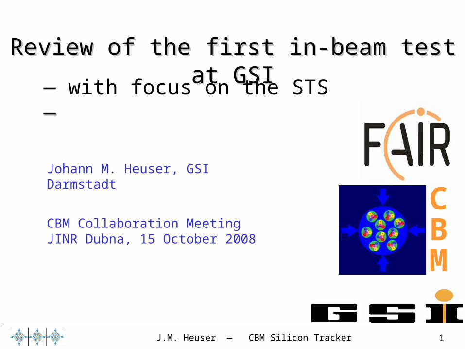
Parasitic to the HADES beam time: 8h*) 2.3 GeV proton beam
Location: GSI, Cave C
J.M. Heuser — CBM Silicon Tracker 3
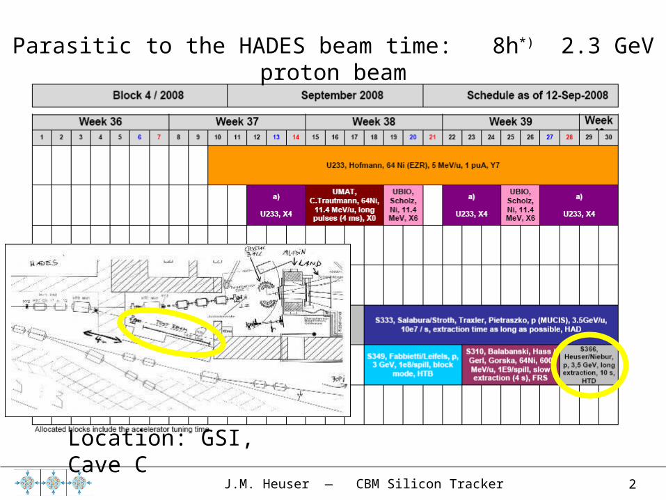
Testbeam SetupTestbeam Setup
design and construction: W. Niebur, GSI
3 CBM experiments (STS, GEM, FPGA + DAQ)1 standalone PANDA experiment (DIRC)
beam diagnostics box
J.M. Heuser — CBM Silicon Tracker 4
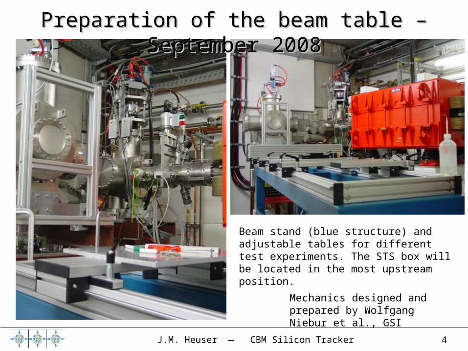
Preparation of the beam table – September 2008Preparation of the beam table – September 2008
Mechanics designed and prepared by Wolfgang Niebur et al., GSI
Beam stand (blue structure) and adjustable tables for different test experiments. The STS box will be located in the most upstream position.
J.M. Heuser — CBM Silicon Tracker 5
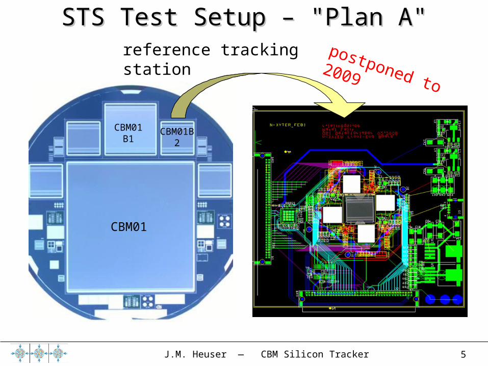
STS Test Setup – "Plan A"STS Test Setup – "Plan A"
CBM01
CBM01B1
CBM01B2
postponed to 2009
reference tracking station
J.M. Heuser — CBM Silicon Tracker 6
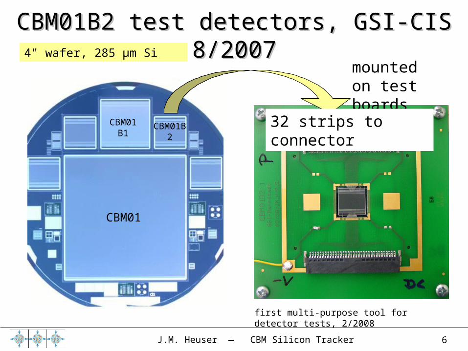
CBM01B2 test detectors, GSI-CIS 8/2007CBM01B2 test detectors, GSI-CIS 8/20074" wafer, 285 µm Si
CBM01
CBM01B1
CBM01B2
mounted on test boards
first multi-purpose tool for detector tests, 2/2008
32 strips to connector
J.M. Heuser — CBM Silicon Tracker 7
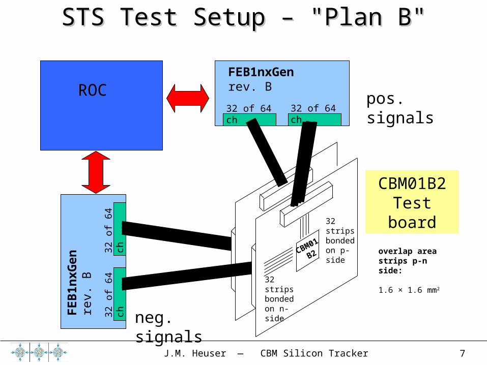
FEB1nxGen rev. B
32 of 64 ch32 of 64 ch
FE
B1n
xGen
r
ev.
B
32 o
f 64
ch
32 o
f 64
ch
ROC
STS Test Setup – "Plan B"STS Test Setup – "Plan B"
pos. signals
neg. signals
32 strips bonded on p-side
32 strips bonded on n-side
overlap area strips p-n side:
1.6 × 1.6 mm2
CBM01
B2
CBM01B2 Test board
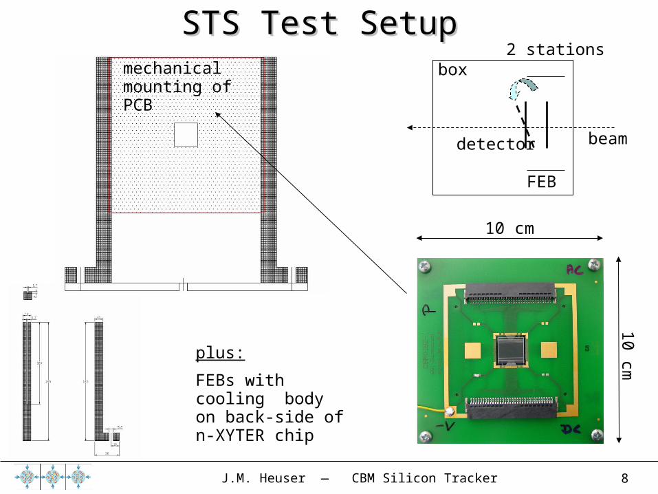
J.M. Heuser — CBM Silicon Tracker 8
STS Test Setup STS Test Setup
10 cm
2 stationsmechanical mounting of PCB
plus:
FEBs with cooling body on back-side of n-XYTER chip
10 cm
box
FEB
detector beam
J.M. Heuser — CBM Silicon Tracker 9
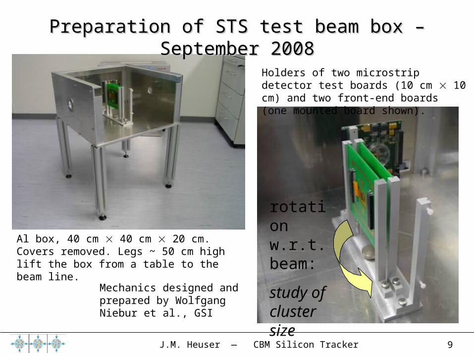
Preparation of STS test beam box – September 2008Preparation of STS test beam box – September 2008
Mechanics designed and prepared by Wolfgang Niebur et al., GSI
Al box, 40 cm 40 cm 20 cm. Covers removed. Legs ~ 50 cm high lift the box from a table to the beam line.
Holders of two microstrip detector test boards (10 cm 10 cm) and two front-end boards (one mounted board shown).
rotation w.r.t. beam:
study of cluster size
J.M. Heuser — CBM Silicon Tracker 10
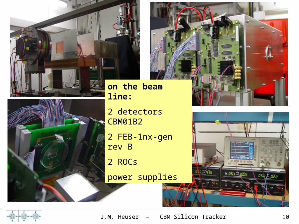
on the beam line:
2 detectors CBM01B2
2 FEB-1nx-gen rev B
2 ROCs
power supplies
J.M. Heuser — CBM Silicon Tracker 11
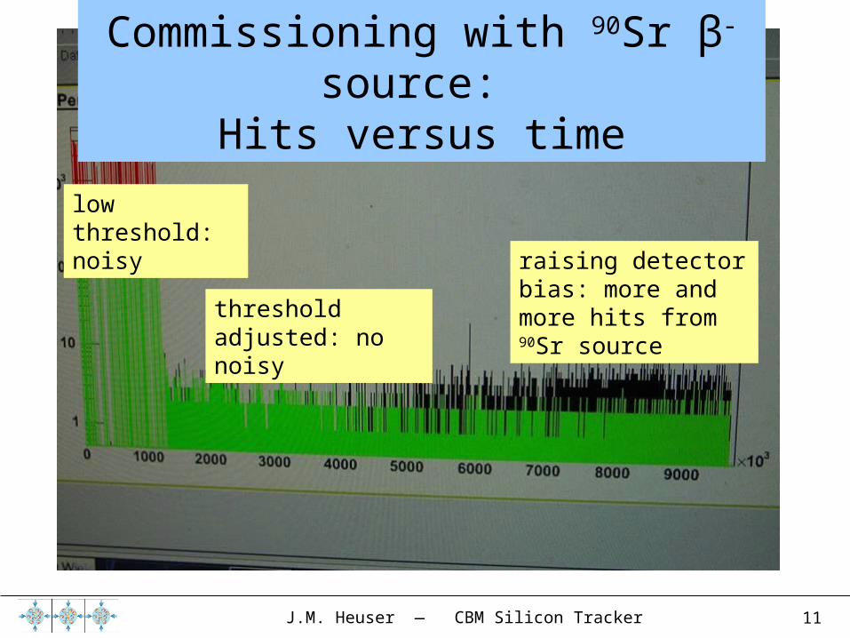
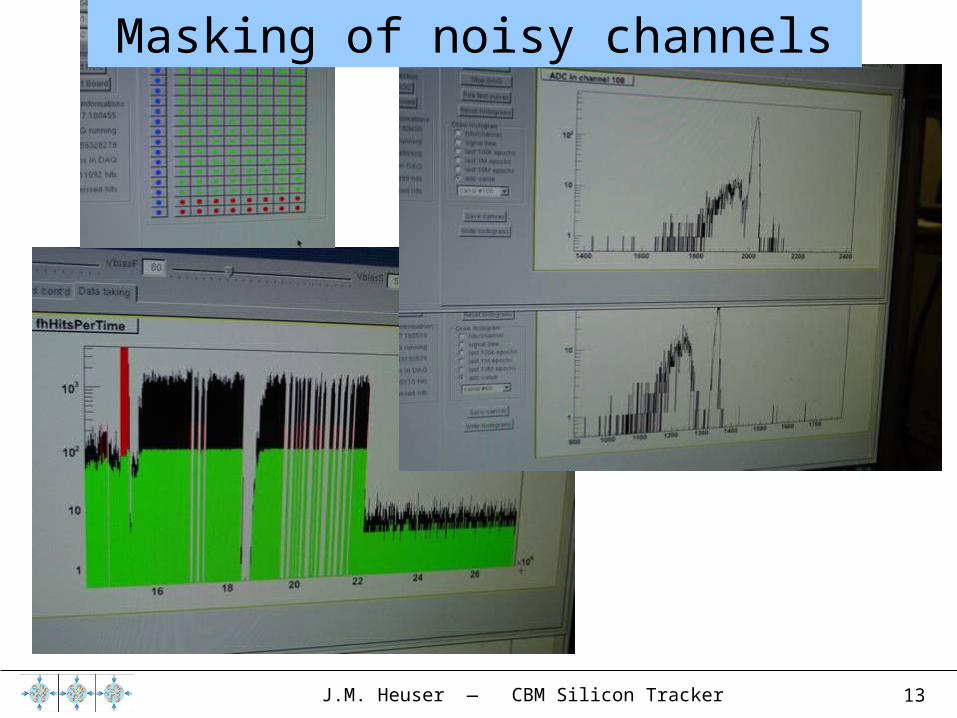
low threshold: noisy
threshold adjusted: no noisy
raising detector bias: more and more hits from 90Sr source
Commissioning with 90Sr β- source: Hits versus time
J.M. Heuser — CBM Silicon Tracker 12
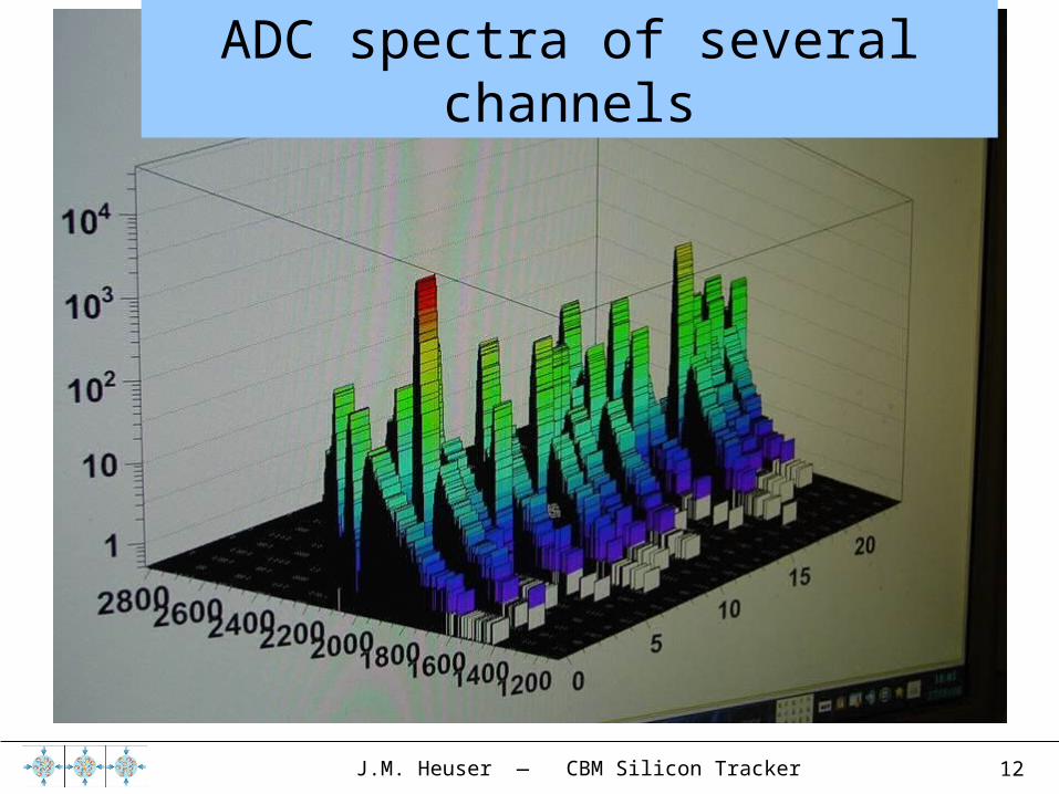
ADC spectra of several channels
J.M. Heuser — CBM Silicon Tracker 13
Masking of noisy channels Masking of noisy channels
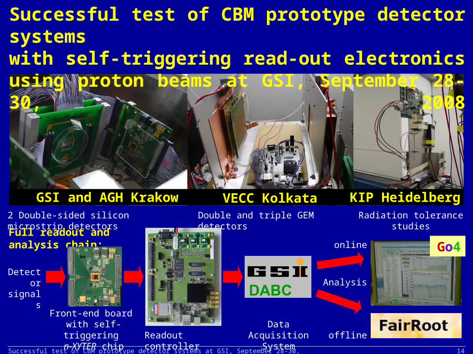
Successful test of CBM prototype detector systems at GSI, September 28-30, 2008 14
Double and triple GEM detectors2 Double-sided silicon microstrip detectors
Radiation tolerance studies
Full readout and analysis chain:
Front-end board with self-triggering
n-XYTER chip Readout controllerData Acquisition
System
online
offline
Go4
AnalysisDetector
signals
Successful test of CBM prototype detector systems with self-triggering read-out electronics using proton beams at GSI, September 28-30, 2008
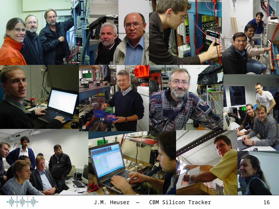
GSI and AGH Krakow VECC Kolkata KIP Heidelberg
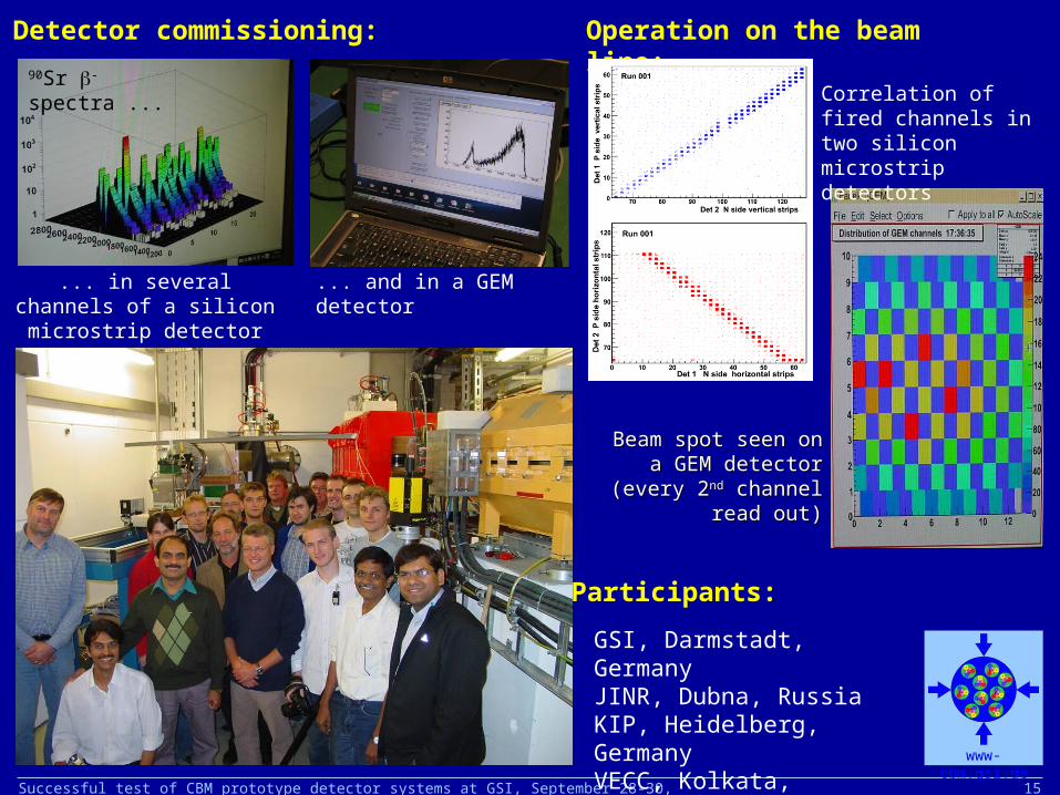
Successful test of CBM prototype detector systems at GSI, September 28-30, 2008 15
GSI, Darmstadt, GermanyJINR, Dubna, RussiaKIP, Heidelberg, GermanyVECC, Kolkata, IndiaAGH, Krakow, Poland
90Sr -spectra ...
Detector commissioning:
... in several channels of a silicon microstrip detector
... and in a GEM detector
Operation on the beam line:
Participants:
Beam spot seen on a Beam spot seen on a GEM detector (every GEM detector (every 22ndnd channel read out) channel read out)
Correlation of fired channels in two silicon microstrip detectors
www-cbm.gsi.de
J.M. Heuser — CBM Silicon Tracker 16
J.M. Heuser — CBM Silicon Tracker 17
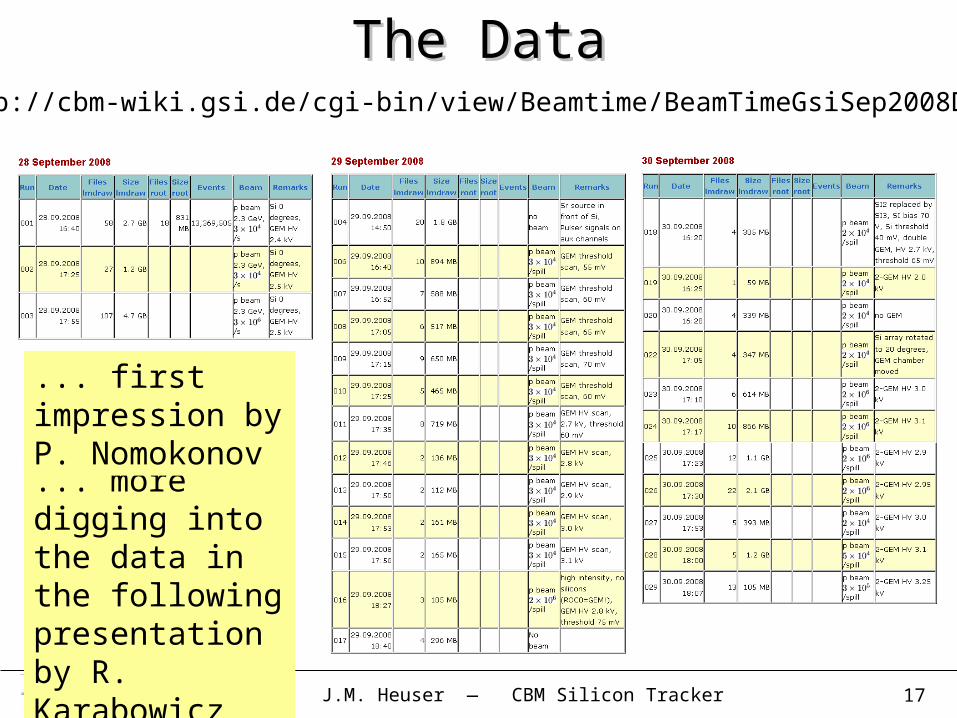
http://cbm-wiki.gsi.de/cgi-bin/view/Beamtime/BeamTimeGsiSep2008Data
The DataThe Data
... more digging into the data in the following presentation by R. Karabowicz
... first impression by P. Nomokonov
J.M. Heuser — CBM Silicon Tracker 18
Summary:
First system tests of STS: Everything new - Detector, FEE, DAQ
4 detector boards produced from tested CBM01B2 sensors
3 boards passed acceptance test – 1 drew current after wire-bonding
2 detector boards installed in beam. Operation: OK
- about 250 nA current in both detectors @ 50 V bias (900 nA @ 70V)
- few noisy channels – can be masked
A third detector:
- started to draw current beyond 20V bias when connected to FEBs - insight into AC insulation quality of CBM01???
We learned already a lot from the commissioning – and first analysis of data.
Follow-up with a long-term setup of the test system in the lab.
J.M. Heuser — CBM Silicon Tracker 19
Radek Karabowicz, Anton Lymanets, Rafal Lalik, Petr Nomokonov,
Wolfgang Niebur, Johann Heuser
The STS Test Beam Team