Embed Size (px)
Citation preview
AD-AO5 090
WIDEBAND SOLID-STATE PHASED-ARRAY ANTENNAA1 9DEVELOPMENT AT UHF
G. J. Laughlin
Johns Hopkins Universityf
Prepared for:
Office of Naval Research
July 1975 1
-i .
DISTRIBUTED BY:
National Technical Information ServiceU. S. DEPARTIENT OF COMMERCE
-----.----.

Unclassified PLEASE FOLO 8ACX IF NOT NEEDED
SECURITY CLASSIFICATION OF THIS PAGE r0R BIBLIOGRAPHIC PURPOSES
REPORT DOCUMENTATION PAGEI REFLOAT NUMBER 2 GOVT ACCESSION NO 3. R4ECIPIENT'SCATALOG NUMBER
r APL/JHU TG 12784- T I TLE Und Subt, leI 5. TYPE OF REPORT & PERIOD COVERED
WIDEBAND SOLID-STATE PHASED-ARRAY ANTENNA Technical MemorandumDEVELOPMEN\T AT UHF
6. PERFORMING ORG. REPORT NUM13ER
7 AUTHOR~s) B. CONTRACT OR GRANT NUMBER(s)
G. J. Laughlin N00017-72-C-4401
9- PERFORMING ORC.ANI ZAT ION NAME &ADRrSS 10. PROGRAM ELEMENT. P'ROJECT, TASK
The Johns Hopkins University Applied Physics Laboratory AE OKUI UBR
8621 Georgia Avenue
Silver Spring, Maryland 2091011. CONTROLLING OFFICE NAME A ADDRESS 12. REPORT DATE
Naval Plant Representative Office July 19"158621 Georgia Avenue 13. NUMBER OF PAGIF-I
1 1 Silver Spring, Maryland 209 10
U 14. MONITORING AGENCY NAUE & ADDRESS 15. SECJRITY CLASS. (ofit repaort)
Naval Plant Representative Office Unclassified8621 Georgia Avenue _____________
Silver Spring, Maryland 20910 S5a.EDL S IAINIENRDN
716. DISTRIBUTION STATEMENT tof 1k,,ReonI N/A
Approved for publi! release; distribution unlimited.
INI
I. STIBUTINTAYNTEETStti~z'c nztS~ SakXSdli~ttoR~g
N/A
19. KEY WORDS (Contiue an reverse sid ifnecessay andidentify by bloc;. Wnbht,)
weArray art eunas Solid-state phased arraysPhased arrays Integrated phased arraysWideband phased arrays BalunsOctave band phased arrays
20. AB3STR ACT (Con tnue an rve wded necessr vnd ,den 9,Iy by bioc& uwnbeai Development of an experimental l6-elemenisolid-state linear phased-array antenna that has an operating band fromr 0. 6 to 0. 95 GHz is de-scribed. Radiating elements in the antenna are novel strip radiators made using printed circuitItechniques. The array aperture has been impedance matched to a VSWR < 3. 0:1 over the octave
band from 0. 5 to 1. 0 GHz with beam scanning to ±60* in the H plane. Element patterns measuredon a 10- by 10-element array aperture indicate that the aperture is also matched with beam scan-
nigto 1609 in the E plane. Each of the rcliators in the 16- element linear array was integratedwith a microwave transistor amplifier with a nominal gain of 10 dB and efficiency of 50% at 3 wattsoutput. Bandwidths of the amplifiers limit the 16-element solid-state array to an operating bandfrom 0. 6 to 0. 95 Gl~z. Beam scanning in the H plane is accomplished by inserting lengths of Co-axia. delay lines between the integrated array and a 16:1 power divider network. Techniques andmethods used in this development are applicable at higher radar frequencies.
FORM A'IU D D IjAN '3 1473 Unclassified
SECURITY CLASSIFICATION OF THISPIAGE
t APL/JHUJ
TG 1278JULY 1975
Technical Memorandum
WIDEBAND SOLID-STATEPHASED -ARRAY ANTENNADEVELOPMENT AT UHFG. J. LAUGHLIN
ITHE JOHNS HOPK INS UNIVE RSITY * APPLI ED PHYSICS L 6,BORATORY8621 Georgia Avenue - Silver Spring, Maryland 20910j Ope~at-g . de, Confla-1 N0001 7 7? C-4401 W.th the Departnit of the Navv
2791 40
~APL/JHU
TG 1278JULY 1975
Copy No. 8
Technical Memorandum
(WIDEBAND SOLID-STATEOPHASED-ARRAY ANTENNA
DEVELOPMENT AT UHF
G. J. LAUGHLIN
DDC-
%D SEP 29 1915 n~Re fa.-J-J hNATIONAL TECHNICAL UUL U
INFORMATION SERVICE BU S D 0oW' cl CFCr -'
THE JOHNS HOPKINS UNIVERSITY . APPLIED PHYSICS LABORATORY
Approved for public release; distribution unlimited.
~AR i • -_
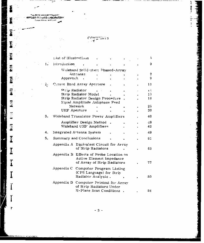
i-ist of llustrmt'.4AO5
1.I lntr od ucLion .9
VWideband Solt1d-stat, Phased-Array
,t n,.t ..tG r**, .,C
. Approach , .. 9:.
, Octave Band Array Aperture . 11
II
1. ntricp Radiator . 9St rip Radiator Model
Strip Radiator Design Procedure . 16Equal Amplitude Antiphase Feed
- Network . .. 25UHF Aperture . . . . 30
e 3. Wideband Transistor Power Amplifiers 40
Amplifier Design Method . . . 40Wideband UHF Amplifier. . 42
4. Integrated Artenna System . . 49
5. Summary and Conclusions . . . 61
Appendix A Equivalent Circuit for ArrayI of Strip Radiators . 63
Appendix B Effects of Probe Location onActive Element Impedance-r of Array of Strip Radiators . 77
Appendix C Computer Program Listing(CPS Language) for Strip
Radiator Analysis . . 80
Appendix D Computer Printout for Arrayof Strip Radiators UnderH-Plane Scan Conditions . 84
r3
APPUED PHYSICS LASORTO'Py
Appendix E Saturated Output Power andEfficiency of RF TransistorsOperating in Class C * 86
Nomenclature . ** * 91
References

APPUSO9 PHYSICS LASWORiY
ILLUSTRATIONS
I Array of Strip Radiators .12
2 Array Simulator Terminated in TwoI Elements . . 14
3 Strip Radiator in Waveguide Simulator 15
4 Equivalent Circuit. Array of StripRadiators (H-plane scan) . 16
5 Resistive Part of Active ElenzentImpedance versus w/dE; ErdEXdH /X =0. 23B .. . 18
6 Resistive Part of Active ElementImpedance versus w/dE; f r 2. 5.dE/X 7dH/IX= 0. 238 .19
7 Resistive Part of Active Element
Impedance versus %/dE;, f 4.dE/X = d I/x= 0. 238 . . . 20
8 Resistive Part of Active Element'r Impedance versus w/dE; cr
9 Resistive Part of Active ElementImpedance versus -./dE;, Cr 2. 5.dE/X,= dH/)X 0. 5 . 22
10 Resistive Part of Active ElementImrpedance versus widE: cr =4dE Ik d11/X - 0. 5 . 23
11 Effects of Probe Separation on Resistive
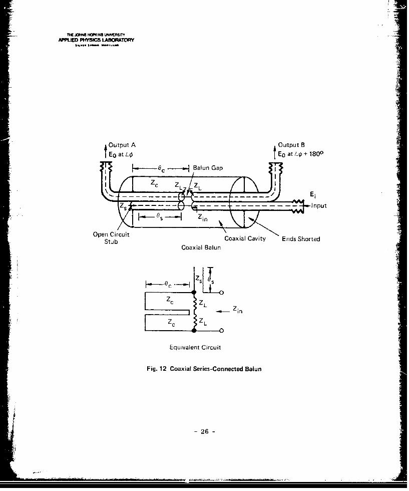
12 Coaxial Series -Connected Halun . . 26
13 Stripline Balun 28
*15
APPUEO PHYSiC LAWMI0AY
14 Measured Results. Strip~Line FBalun .29
15 Strip Radiator Feed IBalun and FeedProbes .. 30
16 Admittance of Simulated Array of StripRadiators . . 32
17 Simulated Array Aperture of PrintedCircuit Radiators 1 3
18 Admittance with WAIM Referenced atWVAIMI Sheet * 35
19 %ISWR of Simulated Array with WAIM . . 36
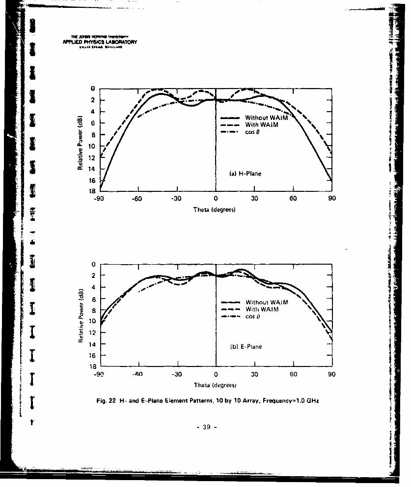
20 H- and E-Plane Element Patterns.10 by 10 Array. Frequenry = 0. 5GRiZ . . 37
21 11- and E-Plane Element Patterns,10 by 10 Array. Frequency =0. 75Gliz 3S.
22 If- and E-Plane Element Patterns.
GHz .* 39
23 Schematic Circuit of the PrototypeAmplifier . .43
24 Load Admittance of the PrototypeAmplifier * 43
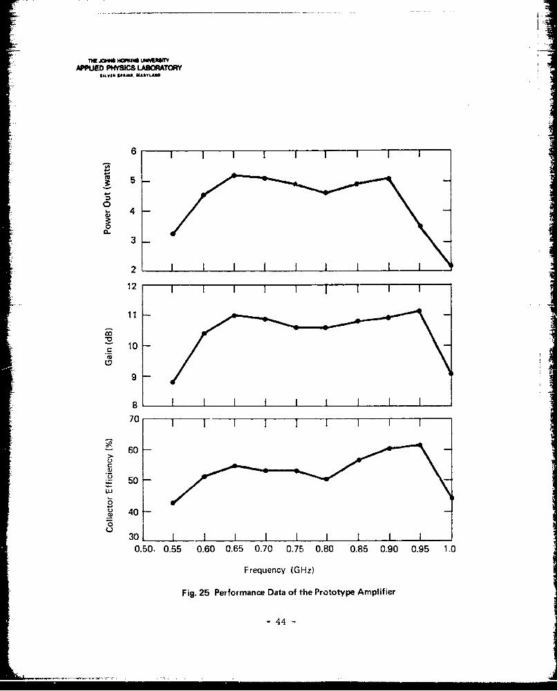
2 5 Performance Data of the PrototypeAmplifier .44
26 The Prototype Amplifier 45
27 Wideband RF Amplifier for Solid-StateArray .. 46
28 Final Performance of the HF A\mplifiers 48
29 Schematic of the 16-Element Solid-StateArray System . . -9
30 Dimensions of the 16-Element Linear'Array Aperture 50
*,L"j PHW.,& LA4OMiOR
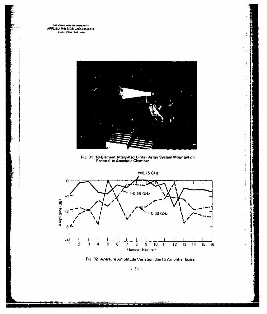
31 16-Element Integrated Linear ArraySystem Mounted on Pedestal in Anechoic
Chamber . . . . . 52
32 Aperture Amplitude Variation due toAmplifier Gains . .
33 Antenna Patterns, 16-Element IntegratedLinear Array. Frequency 0.6 GJz . 54
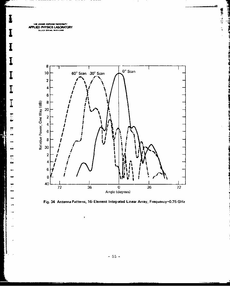
34 Antenna Patterns. 16-Element IntegratedLinear Array. Frequency = 0. 75 GHz . 55
35 Antenna Patterns. 16-Element IntegratedLinear Array, Frequency : 0. 95 GHz 56
36 Gain of 16-Element Linear Array . . 57
37 Element Patterns, 16-Element LinearArray Enclosed in Horn, Frequency 0. 95GHz 58
38 Element Patterns. 16-Element iLinearArray, Horn Removed, Frequency = 0. 95
GHz . . . . . . 60
A-1 Partially Filled Slit-Coupled 7-Junction 64
A-2 Bifurcated T-Junction . 67
A-3 Grating of Posts with Series Resistors . 69
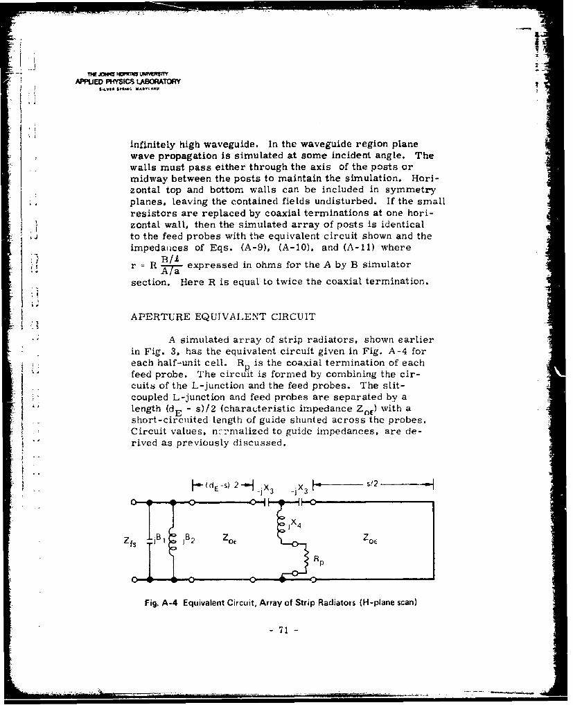
A-4 Equivalent Circuit. Array of StripRadiators (H-plane scan) . . 71
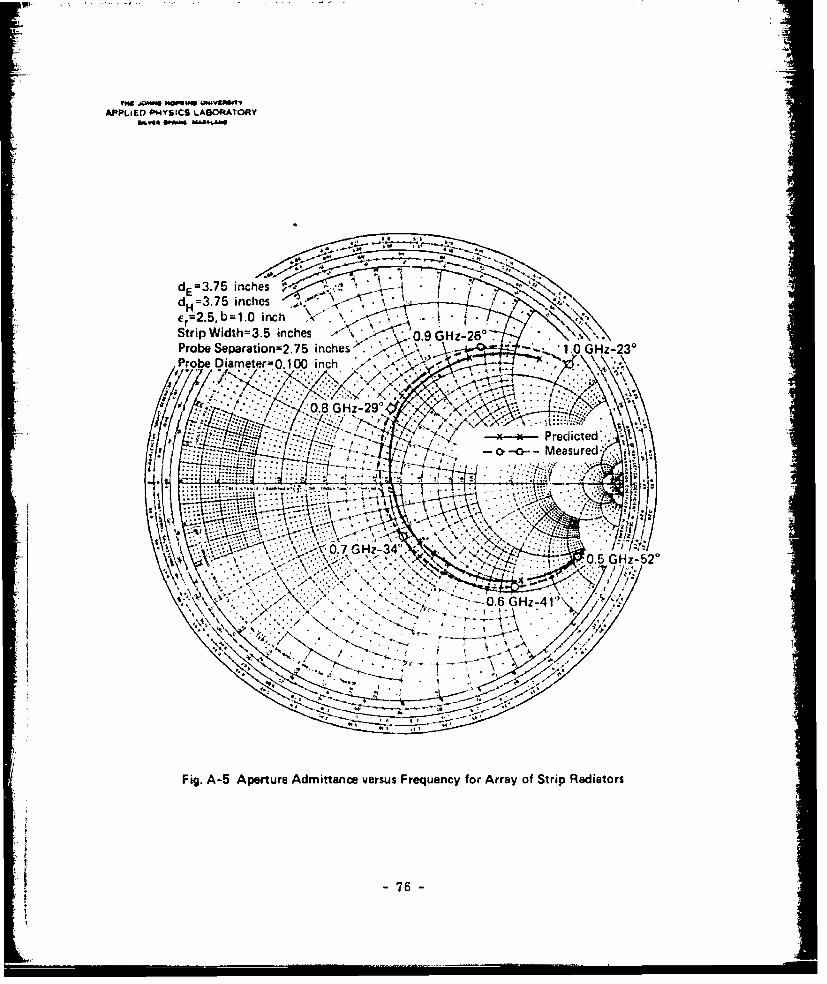
A-5 Aperture Admittance ver,.us Frequencyfor Array of Strip Radiators 76
B-1 Circuit for Effects of Moving ProbesInward from Strip Edges . 78
E-1 Schematic of RF Amplifier and TransistorCollector Characteristics . . 87
-7-
APPED PH3C -40PII,
1. INTRODUCTION
WIDEBAND SOLID-STATE PHASED-ARRAY ANTENNAS
Wideband phased-array antennas have been viewedas a solution to the proliferation of shipborne antenna sys-tems resulting from the many and varied needs on navalSvessels. The present large number of antennas could beconsolidated into a single time-shared wideband aperturewith electronic beam scanning. In recent years. solid-state microwave technology has advanced to the stage whereincreased reliability and efficiency of solid-state devicescan be used advantageously for RF power generation inmodern phased arrays. Integrating wideband solid-statepower devices with a wideband array aperture would re-sult in a highly reliable system with increased efficiencybetween DC power generation and RF transmission. re-duce the number of shipborne antennas, and provide en-
-- hanced operational capabilities in an unfriendly environ-ment. Also the wideband antenna capabilities have clearpotential for countermeasure applications, both passivef and active.
A wideband solid-state phased-array antenna withwide angle scanning was developed to demonstrate the feasi-
bility of such a system for eventual shipborne application.An experimental very wideband system with beam scanningto *60" was built for operation at UHF frequencies. Thiseffort included investigations of techniques required to de-sign an octave band (0. 5 to 1. 0 GHz) array aperture andmethods for tize efficient wideband generation of RF power.Designs used in this system were to be adaptable to higherradar frequencies.
V APPROACH
Radiated power from a solid-state antenna aperturecan be increased if the solid-state devices are in+egratedwith electrically ,,mall radiating elements. Tl c!ements
-9-
Preceding page blank
L
AUM MHYC LABORATORY
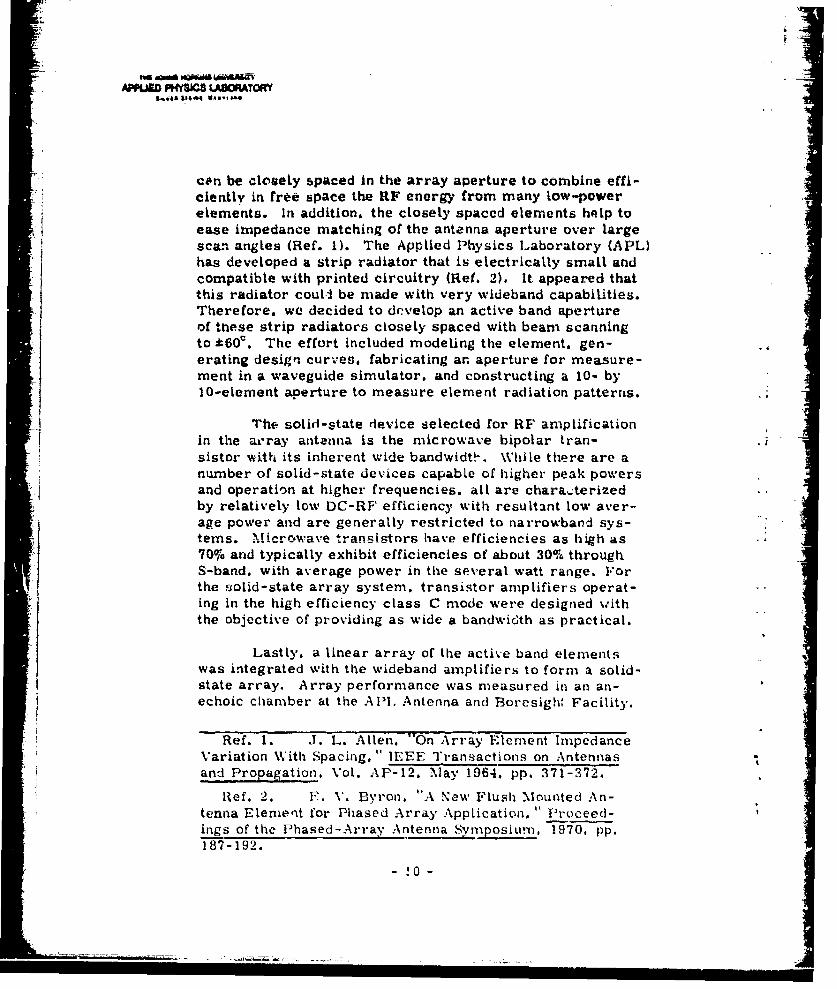
con be closely spaced in the array aperture to combine effi-ciently in tree space the RF energy from many low-powerelements. In addition, the closely spaced elements halp toease impedance matching of the antenna aperture over largescar. angles (Ref. 1). The Applied Physics Laboratory (APL)has developed a strip radiator that is electrically small andcompatible with printed circuitry (Ref. 2). It appeared thatthis radiator coul-i be made with very wideband capabilities.Therefore. we decided to develop an active band apertureof tnese strip radiators closely spaced with beam scanningto *600 . The effort included modeling the element, gen-erating design curves, fabricating an. aperture for measure-ment in a waveguide simulator, and constructing a 10- by10-element aperture to measure element radiation patterns.
The solid-state device selected for RF amplificationin the array antenna is the microwave bipolar tran- .sistor with its inherent wide bandwidth. While there are anumber of solid-state devices capable of higher peak powersand operation at higher frequencies. all are chara,;terizedby relatively low DC-RF efficiency with resultant low aver-age power and are generally restricted to narrowband sys-tems. Microwave transistnrs have efficiencies as hih as70% and typically exhibit efficiencies of about 30% throughS-band. with average power in the several watt range, Forthe solid-state array system, transistor amplifiers operat-ing in the high efficiency class C mode were designed withthe objective of providing as wide a bandwidth as practical.
Lastly, a linear array of the active band elementswas integrated with the wideband amplifiers to form a solid-state array. Array performance was measured in an an-echoic chamber at the APL Antenna and Boresighl Facility.
Ref. 1. J. L. Allen, "On Array Element ImpedanceVariation With Spacing, " IEEE Transactions on Antennasand Propagation, Vol. AP-12. May 1964. pp. 371-372.
Ref. 2. F. V. Byron, "A New Flush Mlounted An-tenna Element for Phased Array Application." Proceed-ings of the Phased-Array Antenna Symposiurn, 1970, pp.187-192.
-0-

AD9UX PWYS9t UABORATORY
2. OCTAVE BAND ARRAY APERTURE
STRIP RADIATOR
Development of the octave band antenna is based ona phased-array radiat.ng element, the strip radiator, thatwas developed for Project Camel (Refs. 2 and 3). Attrac-tive features of the element are that it is configure] usingprinted circuit techniques, it is suitable for integrationwith solid-state djevices. and it can be densely packed inan array aperture.
Figure I shows an aperture of the strip radiatorsthat was developed for Project Camel. It consisted of anarray of conducting strips situated above a ground planeii where a. suitable dielectric filled the region between groundplane and strips. The strips were nominally a half wave-lergth wide in the dielectric and were excited periodicallynear the edges by probes extending through the groundplane. On each strip, probes were rlaced opposite one an-other and near the edge. The two probes at opposite edges
Swere driven in antiphase with equal amplitudes. That de-velopment resulted in array apertures with half wavelength
Lelement spacing and bandwidths on the order of 10 to 121 ..For Project Camel. the emphasis was on antennas with ele-rnents spaced very close to the ground plane.
In the present wcrk, we felt both that a very wide-band antenna aperture could be achieved by increasing the
I spacing between strips and ground plane and that close ele-ii ment spacing could be easily obtained in the Il-plane by
moving adjacent pairs of feed probes close together. Origi-nally it was thought that close L-plane spacing could be
1 achieved by dielectric loading to make the strips narrow(X/2 in the dielectric), but. as the discussion of the stripradiator model ir, the next subsection shows, narrow stripsand close E-plane spacing can be accomplished even with-out dielectric loading. The need for a compact and wide-band antiphase power divider for driving the elements was
Ref. 3. E. V. Byron. Antenna Aperture Design for
Project Camel. APl./J"l' TG 1101. FeLruary 1970.- 11 -
APPLIED PHIYSICS LABORATORY
CL
to 0
~o. 0~ 0
121
APPLIED PHYSICS LABORATORYsi@&&pw". U.S,A'
recognized. +his required an additional development effortwhich is discussed in the subsection on the antiphase feednetwork.
Aperture resonance, which can be initiated by di-electric impedance matching sheets on an array aperture,was the limiting factor in an earlier wideband antenna de-sign (Ref. 4). To avoid these resonances as much aspossible with the strip radiators, where dielectric loadingis inherent in the design, the aperture impedance match-
I ing was implemented in this design by networks behind theaperture rather than by additional dielectric sheets.
STRIP RADIATOR AIODEL
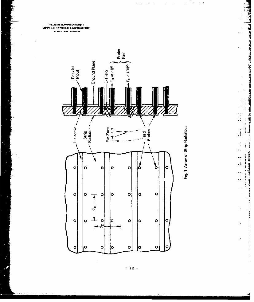
I A large planar phased-array aperture can be simu-lated with relatively few elements in waveguide to deter-mine aperture radiation performance (Ref. 5). A wave-
I guide excited in the TE, 0 mode nay be considered to con-tain two inclined plane waves propagating down the guide.The angle each of the plane waves makes with the longitu-Idinal direction (Fig. 2) is determined by the H-dimensionof the waveguide and E mu lates the angle of scan of an in-finite array:
sin - /X . (1)c
Additional scan angles may be simulated by exciting othermodes. The waveguide dimensions are chosen so that a
I radiating element (or elements) placed in the waveguide
Ref. 4. G. J. Laughlin, E. V. Byron, and T. C.Cheston, "Very Wideband Phased-Array Antenna," IEEETransactions on Antennas and Propagation. Vol. AP-20.November 1972. pp. 699-704.
Ref. 5. P. W. Hannan and M. A. Balfour. "Simula-tion -1 a Phazs.-Array Antenna in Waveguide. " IEEE Trans-
Sactions on Antennas and Propagation. VoL. AP-13. May 1965.pp. 342-353.
- 13-
- r!... f *
APPUED PHYSIC LABOR *TOW~
II.. . .. U.4*A3LAi
E-Dimension E-F ield
Side View
Ac=2A Plane Wave Propagation
H-Dimension /
Top ViewTerminated Radiators
Fig. 2 Array Simulator Terminated in Two Elements
sees mirror images in the walls of the guide that appearto be at the same spacing as the array to be simulated. -Excitation of the waveguide in the TE 1 o mode simulatesH-plane scanned conditions on the infinite array.
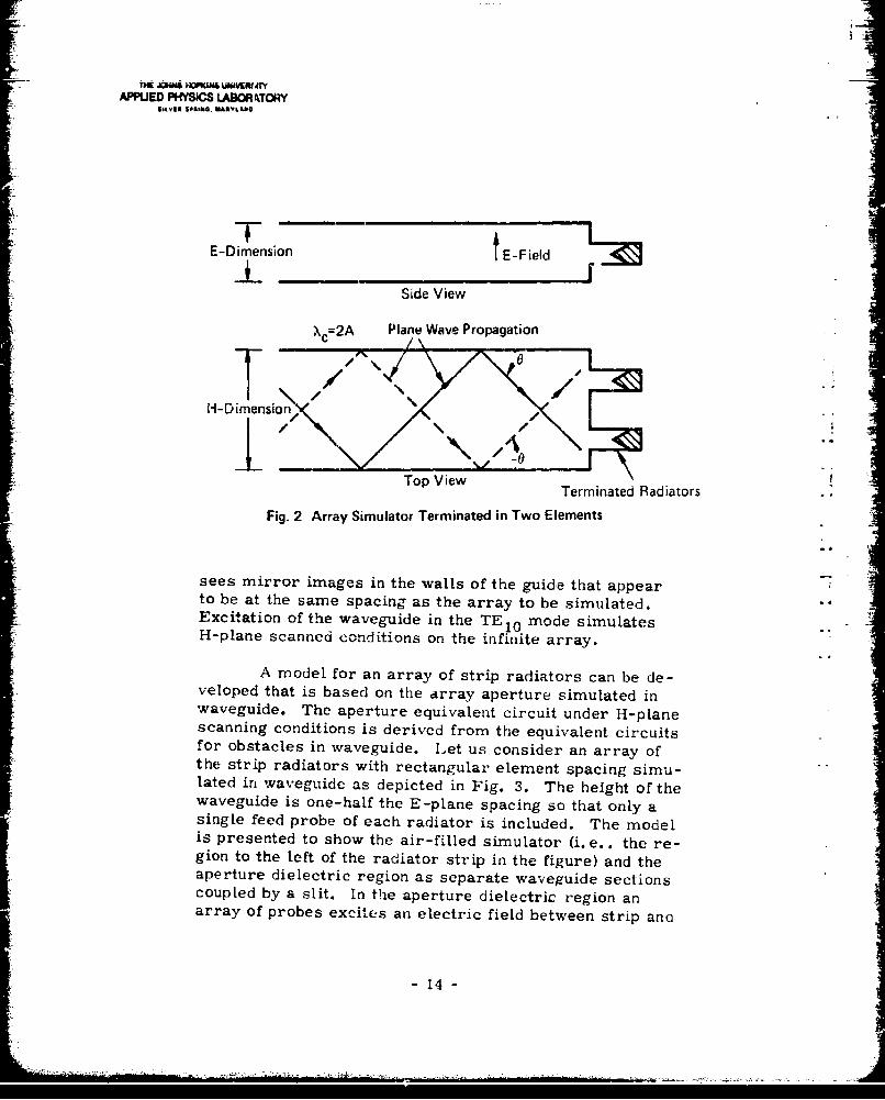
A model for an array of strip radiators can be de-veloped that is based on the array aperture simulated inwaveguide. The aperture equivalent circuit under H-planescanning conditions is derived from the equivalent circuitsfor obstacles in waveguide. Let us consider an array ofthe strip radiators with rectangular element spacing simu-lated in waveguide as depicted in Fig. 3. The height of thewaveguide is one-half the E-plane spacing so that only asingle feed probe of each radiator is included. The modelis presented to show the air-filled simulator (i. e. . the re-gion to the left of the radiator strip in the figure) and theaperture dielectric region as separate waveguide sectionscoupled by a slit. In the aperture dielectric region anarray of probes excites an electric field between strip ana
14-
- L -
APPiED PhIYC USCRMTOFr
I MEI IEffII
I i-ildStrip Dielectric-F illedAir-Filled Radiator Region
Region (Simulator) Re
r Feed Probew/2 -
dE E Coaxial InputRectangular -j-- 'f
d Waveguide =
_| ]
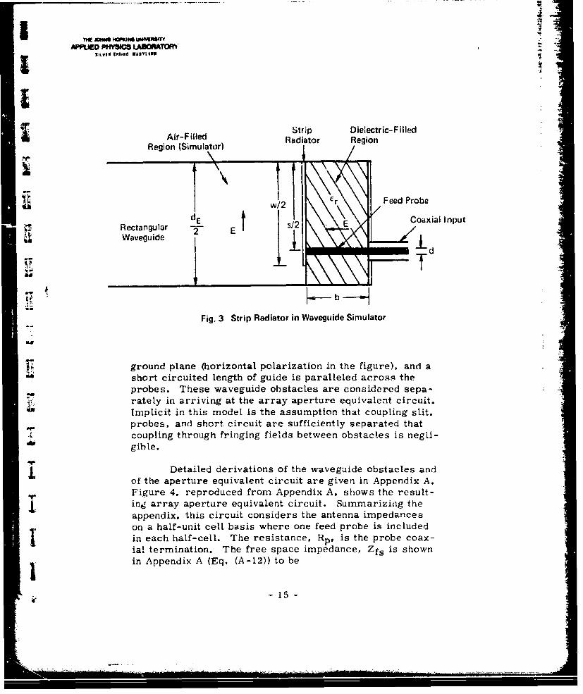
Fig. 3 Strip Radiator in Waveguide Simulator
17 ground plane (horizontal polarization in the figure). and ashort circuited length of guide is paralleled across theprobes. These waveguide obstacles are considered sepa-rately in arriving at the array aperture equivalent circuit.Implicit in this model is the assumption that coupling slit.probes, and short circuit are sufficiently separated thatcoupling through fringing fields between obstacles is negli-gible.
j Detailed derivations of the waveguide obstacles andof the aperture equivalent circuit are given in Appendix A.Figure 4. reproduced from Appendix A. shows the result-ing array aperture equivalent circuit. Summarizing theappendix, this circuit considers the antenna impedanceson a half-unit cell basis where one feed probe is included
I in each half-cell. The resistance, Hp, is the probe coax-ial termination. The free space impedance, Zfs is shown
. in Appendix A (Eq. (A-12)) to be
-15-

FEj0 lI - OK0 NC WW FAAPPfr PHSC8 LORKTORY
2~.a.
d ) x3 -jx3
-0" 0 L 0
Zfs 2 z zo
R: p
C : 0 0'0
Fig. 4 Equivalent Circuit, Array of Strip Radiators (H-plane scan)
zfs = (d /d ) x/cos 0
Equations (A-17) through (A-23) give the remaining imped-ance elements in the equivalent circuit.
STRIP RADIATOR DESIGN PROCEDURE
The method for designing an array of printed cir-cuit radiators with given E- and H-plane spacings considersthe center frequency broadside active element impedance ofa half-element as seen at the feed probe inputs. The feedprobes are assumed to be purely inductive in this proce-dure (i.e. , in Fig. i X 3 = 0). Element parameters arechosen to make the resistive part of the active element im-pedance (of a half-element) equal to the coaxial termination(generator) impeda.ice at each probe, typically 50 ohms.The antenna reactaice is cancelled by selecting the probedimensions and, if necessary, inserting a capacitor inseries with the probe. In the case of ribbon probes, the
-16-
4
THE J0NG HOPKIN UIFlEMrY
APPLIED PH{41CS LABORATORY
best capacitor location has been found experimentally to bemidway between strips and ground plane.
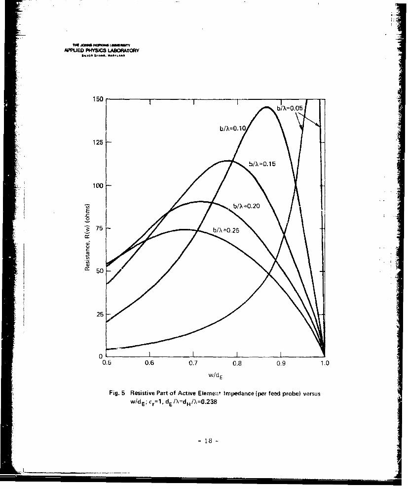
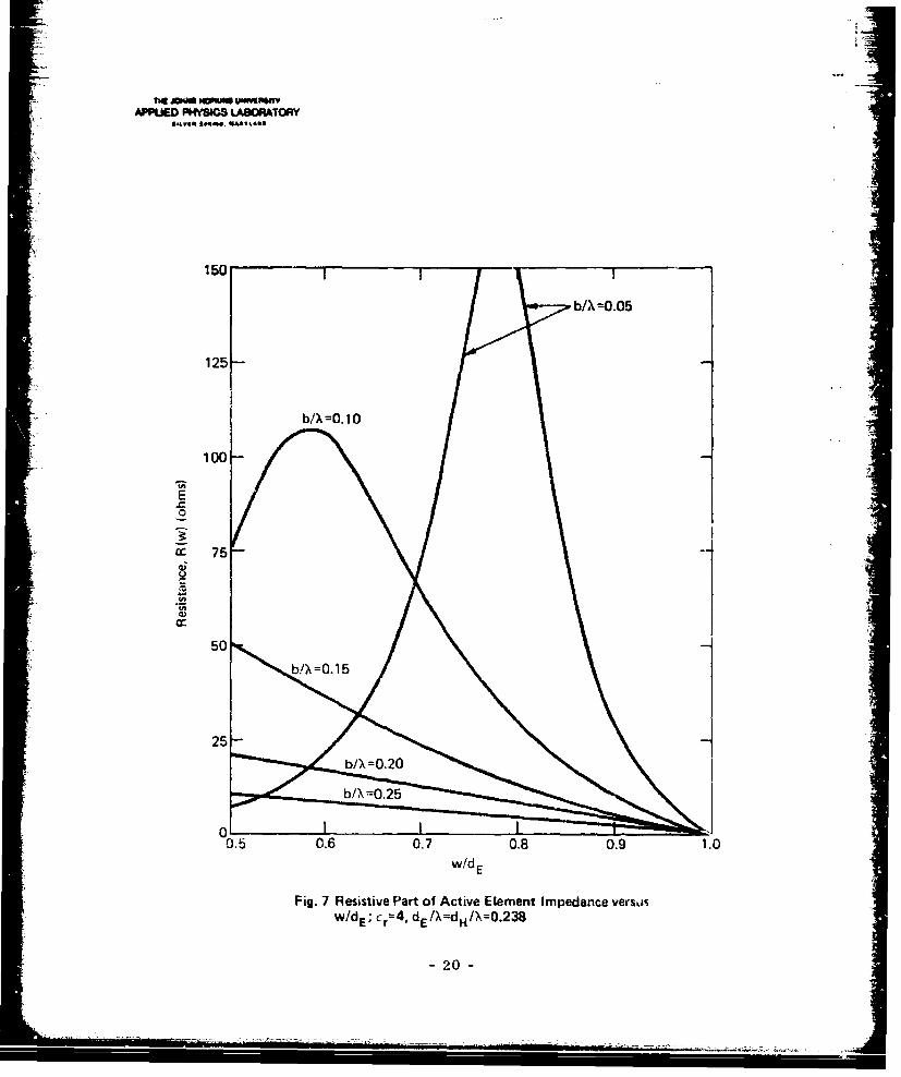
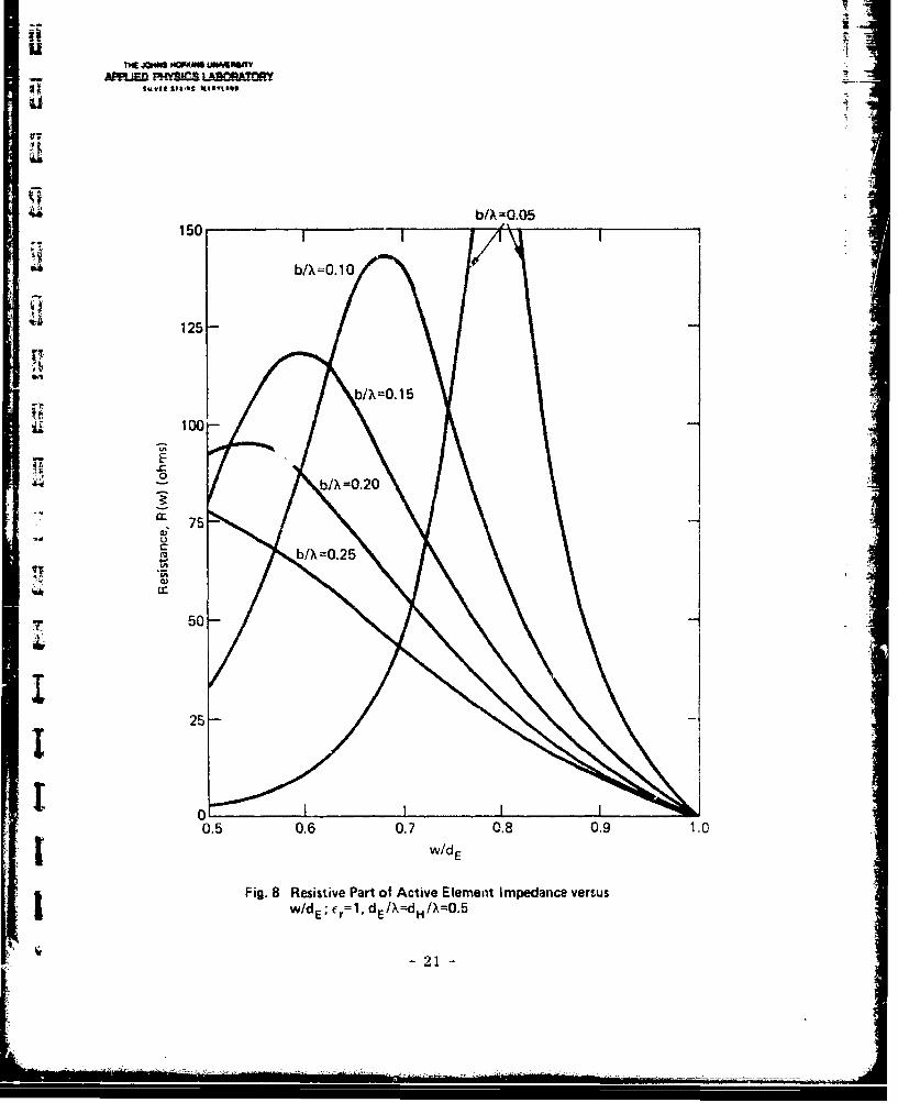
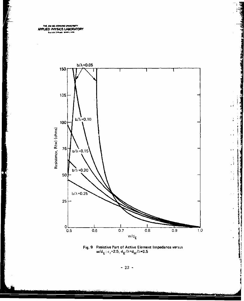
The first step in the design is to plot the re-sistive part. R(w), of the active element impedance forthe feed probes located at the strip edges. Curves of Rr(w)
7- versus w/dE for the specific examples of square spacingwith dE/X = 0.5 and 0.238 and for several values of dielec-
ltric constant, lr' are given in Figs. 5 through 10.
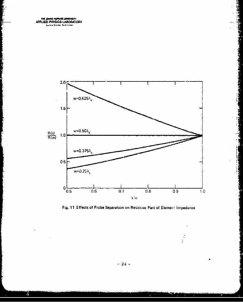
Secondly, the effects of moving the probes inward
from the strip edges are determined. An analysis of theeffects on the resistive part of the broadside active ele-ment impedance, given in Appendix B, results in Eq. (B-5):
Wr
/Q( - s /W) 8 /2)R(s) -w
R(w) tan (BE w/2)
This equation is plotted in Fig. 11. The resistance changewith probe location is used to adjust the resistance, R(s), to
,. match the coaxial termination.
Summarizing, the design procedure is to select a
convenient set of values for aperture dielectric, thickness,and strip width using Figs. 5 through 10. The probe sepa-ration is picked using Fig. 11 to adjust R(s) to match theprobe termination (generator) impedance. For the selectedparameters the resulting reactance is cancelled by choosingappropriate probe dimensions according to Eq. (Z -20) fromAppendix A and, if necessary, incorporating a series capaci-tor .n each probe. It is then necessary to computer ana-lyze the designed aperture to examine bandwidth and scan-ning capabilities, using several iterations of designs fromthe above procedure to meet specifications.
I
-- 17
APPIED PHYSICS LAB0PATOA
b/X=0.O5
b/X=0.1O
125
100
0
0
0.5 0.6 0.7 0.8 0.9 1.0
widE
Fig. 5 Resistive Part of Active Element Impedance (per feed probe) versuswidE; Er=l, dEIN=dH/X=O.23B
is8

APPUE 0 PtYW8 LAOOATOAkY
150
u b/X=0.05
125
blX =0.10
100-
0J
sit C
K; ~ 75
50b/X=0-20 i',
b/X =0.25"
25.1-i
0 _ _ _ _ _ _ _ _ _ _ _ _ _ _
0.5 0.6 0.7 0.8 0.9 1.0
., w/dE
Fig. 6 Resistive Part of Active Element Impedance versus- w/dE; er=2 .5, d E/X=dHt=0. 2 38
-19-S.- - ~ . -. ..
IMu -W -DVJ UW4F&M'rAPPIED PHYSCS5 LABGAIATOAY
150
b/X =0.05
125-
b/X=0.1O
100-
0
c~75-
a:50
b!?i=0.15
25-
b/\,=0.20
b/X- =0.25
010.5 0.6 0.7 0.8 0.9 1.0
wdE
Fig. 7 Resistive Part of Active Element Impedance versisw/dE; cr 4 , dE/X=dH/X=O. 2 38
-20-
UU
to% AW4 MOP"" ~WvAPPUD MC&LASMA!QY
b/A -O.05150
125-
0 b]X=O.20
a:
CD
50-
25-
0,
0.4.)0 1 'l . .
0.8 0.9=0.0
I w/dE;fr= 1, d E/XH/O.
-21-
APPUED PHYCS LAOMORY
bIX =0.05______ ___
150 r T
125
b/X0.1()
100 =.2
0
2 5
0.5 0.1 0. . . . .
bfdE cr0.20 dEXd/=.
252

50
1' 40
b/?N z0.25
S300fl b/X =0.20
S20
*10
w/dE
Fig. 10 Resistance Part of Active Element impedance versus
w/dEcr 4, d E/dH/N4.5
9- -23-
2.0f~ r
1.LW::O.625Xt.
R)1.0 -
05-
050.6 0.7 0.80-1.
Fig. I1I Effects of Probe Separation on Resisti&ve Part of Elememr Impedance
-24
APPLUfD P94YOS LASOPATORY
EQUAL AN1P1 ATU DE ANITI PHASE FLED NETWORK
As discussed previously. the strip radiator re-quires the two feed probes to be driven in antiphase andequal amplitude over an octave bandwvidth. It is desirableI to achieve this by means of stripline circuitry. A devicethat can perform the antiphase an,! eq-ial amplittude fu.nc-tion is a modified balanced-to-unbalanced transmission
line converter (the balun) in which the balanced line is inthe form of a pair of ant iphase unbalanced lines. Severalauthors have described balutis that operate o-ver wide fre-quency rarges (Refs. 6 through 11). A series -connectedbalun developed for the strip radiator differs from ',heearlier devices by its nietnod of achieving input -to-output
coupli: g, resulting in an easily fabricated balun applicableto strip-line circuitr-y.
The coaxial circuit of the balun for the strip radia-tor is showni in Fig. 12 (from Ref. 12). The outer conduc-
Ref. 6. N. Marchand. "Trans mission -Line Conver-sion." Electronics. Vol. 17. December 1944. pp. 142-145.
£Ref. 7. W. K. Roberts, "A New Wideband Balun,"Proceedings of the IRE, December 1957. pp. 1628-1632.
Ref. 8. J. W. Nlcl.aughlin. D). A. Dunn. and 11. W.Grow. "'A \\ideband lBalun. IRE Transact ions on Micro-wave Theory and T lues. Vol. NMTT-6. July 1958.
Ref. 9. R. I-3awer and .1. J . Wolfe, "A Pr'inted ('ir -cuit Balun for Use With Spir-al Antennas, "IRE Transac-tions on Mlicrowave 'I'heory and Techniques, Vol. NITT-8.'May 196C. pp. 319-325.
Ref. 10. G. Gitman. 'The Compeusated Balun.'IEEE Transactions of Mlicrowave Theory and Techni,,ues.Vol. NMTT-14. March 1966, pp. 112-119.
- Ref. 1.1. 11. R. Phelan, "A Wideband Parallel -con-nected lBalun. " IEEE Transactions of Mlicrowav e TIheoryand Techniques, Vol. NITT-18. May 1970, pp. 259-263.
Ref. 12. G. I.. Laughlin,. Patent 3. 827. 001. July1974.
-25-
APPLIED PHYSICS LABORATORY
t Output A Output BE0 at LO E0 at Lo+ 1800
Coxa Baluna
zc zL Z L
zL Z
Equvaen Circuit
Fig. 12 Coaxial re-oce Balun
Z 26
'*1rs
fM JOHNS HOPKINS wieftarsnVDPUED PHYSICS LABSQ~RATf
tors of adjacent coaxial lines are joined together. A cavity,nominally a half wavelength long, encloses the balun and isshorted to the coaxial lines at each end. A balanced paral-lel line output may be formed if the output lines are bent[ together outside the cavity and the center conductors ex-tended forming a parallel transmission line. Coupling inthe balun occurs at the gap formed by a break in the outerconductors of the coax!al lines across which an electricfield is excited by an incident power flow in the input line.An electric field could also be excited if outputs A and Bwere driven in antiphase and equal amplitude. If a fieldis excited across the gap due to RF flow in a coaxial line,then, by reciprocity, an impressed electric field acrossthe gap will induce power flow in the line. Thus, the fieldexcited by the input coaxial lines couples RF powers intothe output coaxial lines. For a small gap (%X/100) the ex-
I cited field is uniform, and the coupled powers are equalamplitude and in antiphase. Impedances of the outputs are
r series connected as shown in the equivalent circuit.
The enclosing cavity has the effect of paralleling apair of series-connected short circuit stubs (X/4 long)across the series-connected loads. Each of the short-cir-cuit stubs is coaxial, with the outer conductor being thecavity and the center conductor being the shields of the en-*1 closed coaxial lines. In Fig. 12, an open circuited stub,nominally a quarter wavelength long, is connected directlyto the input line and appears in the equivalent circuit as aI reactance in series at the input. The presence of the stubmakes the balun "compensated. " This stub can be replacedby a dummy solid rod that maintains gap symmetry and re-I sults in an "uncompensated" balun. The input impedanceof the compensated balun as seen within 'he input line andreferenced at the gap is
Z Z tan 8 cot 0 + j ZL( 2 Z tan 8 -Z cot )Z. CS C S(2)
in Z + j Z tan 0 (L C c
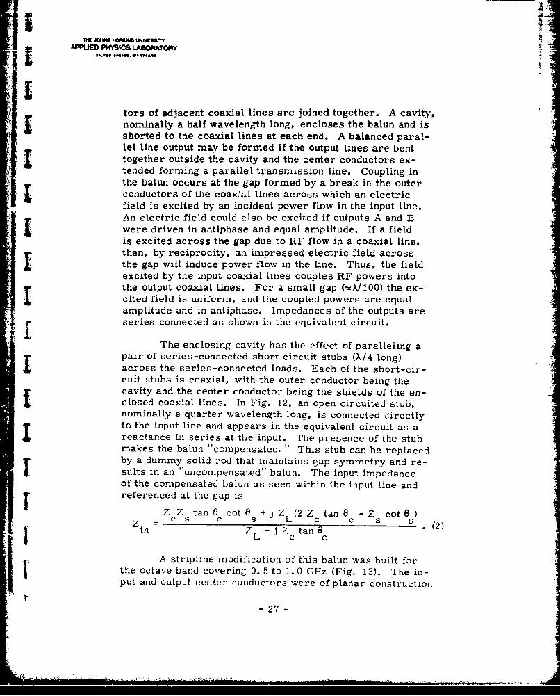
A stripline modification of this balun was built forthe octave band covering 0. 5 to 1. 0 GHz (Fig. 13). The in-put and output center conductors were of planar construction
- 27 -
-4 , -.---
- OH A CO~ UMVRSAPPiED PHYSCS LABORATORY
Fig. 13 Stripline Balun
on a stripline substrate (Cr = 2. 5, b = 0. 167 inch). The outer
conductors wxL e etched lines 1. 27 inches wide such thatone pair of upper and lower lines enclosed the center con-du,:Aors, the pair being joined by eyelets. We eliminatedthe shielding betweea input and output center conductors(normally formed by eyelets) from the design by separat-ing the conductors so that line coupling was less than 30 dB.Balun coupling was through a 0. 100-inch gap in the outerconductor. The design, which was for 50-ohm irnuL andoutput impedances, was achieved by including a 35-ohmquarter wavelength transformer in each output arm. Theoutput ports were spaced 2. 75 inches apart to meet require-ments of the strip radiator discussed in a following subsec-tion. The balun cavity was formed by a dielectrically filled(Er = 2. 5) rectangular box 1. 125 inches high giving a cavityimpedance of approximately 50 ohms. The total cavitylength was shortened to 0. 28 X at midband to accommodatethe required spacing at the output ports. Impedance match-ing, required because of the shortened cavity, was done ex-perimentally and resulted in placing a compensating 38-ohm
- 28 -
- - - - - --
?TE JOHNS HOIKWa L"O"emar- APPLIED PKYSMC LABORATORY
SIL.VER SPAIWG. WEALAIID
open circuit stub 0. 13 inch wide and 0. 18X in length at mid-band, and placing capacitive stubs, located at the gap, on
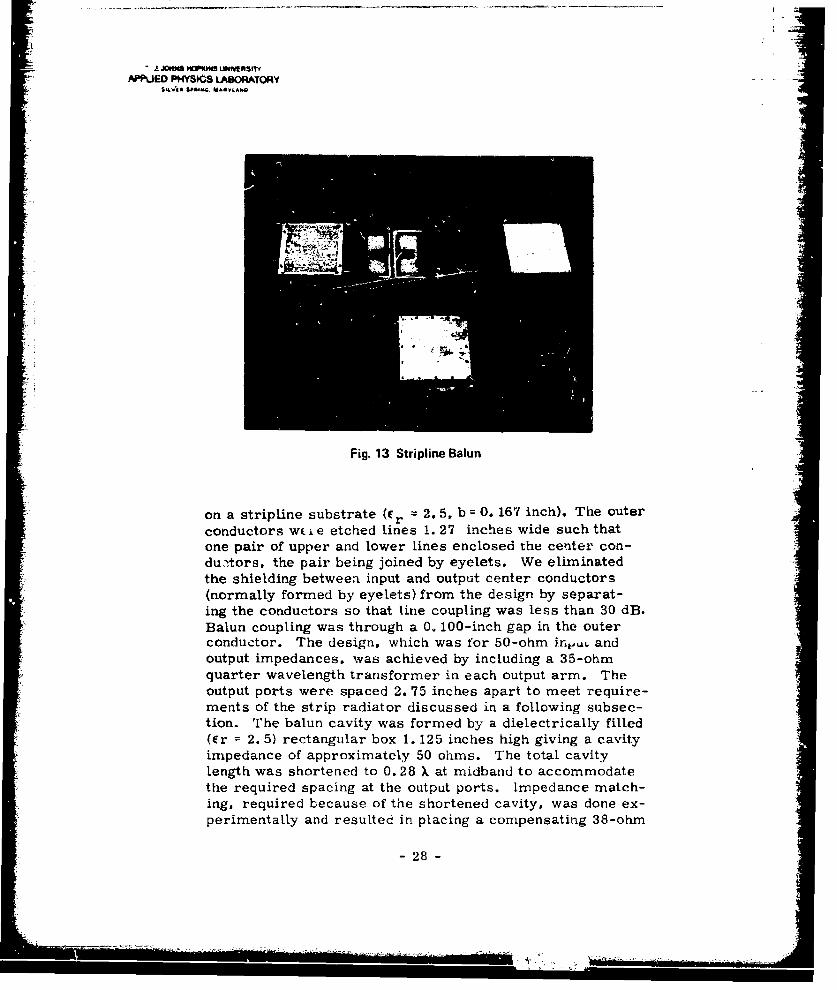
AS the coaxial outer conductor. Measured results of the feednetwork are given in Fig. 14. The input VSWR over theoctave band is under 1. 5:1. insertion loss is less than0. 4 dB, and maximum phase error is 2. 60.
-3.P Output A'
"L --.
~.-3.3- "ry-C
Output B -
4.00
*U 0
1.4-: ~1.3
> 1.2
1.0
Frequency (GHz) 0.09
Fig. 14 Measured Results, Stripline Balun
For application with the strip radiator. we enlargedthe balun stripline substrate and extended the output center
* conductors as shown in Fig. 15. The extended conductorsform the feed probes and are soldered to the radiating ele-ment strip. A gap is etched in each probe to accommodatea 2. 2-pF capacitor included in the element design.
-29-

TI EJ HIS INS U ErSlrtY
APPUED PHYSICS LABORATORYSnkVmal Sd.w& M.S.,..,
Fig. 15 Strip Rediator Feed Balun and Feed Probes
UHF APERTURE
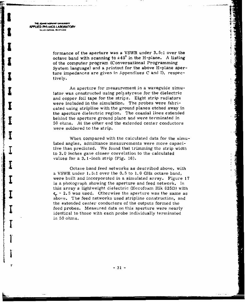
An array aperture of the strip radiators was de-signed for the octave band covering 0. 5 to 1. 0 GHz. Theantenna used square element geometry with close E- andH-plane spacing of 3. 75 inches (0. 238 X at midband). Aper-ture excitation was by flat probes oriented such that eachpair of probes in an element was coplanar (perpendicularto strip edges). The design was that each probe terminatedin 50 ohms.
Design parameters for the aperture, based on thecomputer analysis of bandwidth and scanning performance,were an aperture dielectric 1. 5 inches thick with cr = 2.5,a strip width of 3. 1 inches, and probe separation of 2. 75inches. Referring to the design curves, we found that thisconfiguration yielded an active element impedance at mid-band with a 57-ohm resistive part. The reactance, obtainedin the aperture analysis, was cancelled by making the probewidth 0. 200 inch and incorporating a 2. 2-pF capacitor inseries, located midway in the dielectric. Predicted per-
- 30 -
Mrs J6H** ",AftwVtl"uH(IAPPLIED PM-6ICS LABORATORY
formance of the aperture was a VSWR under 3.5:1 over theoctave band with scanning to 1:450 in the H-plane. A listingof the computer program (Conversational ProgrammingSystem language) and a printout for the above H-plane aper-ture impedances are given in Appendixes C and D, respec-
tively.
An aperture for measurement in a waveguide simu-
lator was constructed using polystyrene for the dielectricand copper foil tape for the strips. Eight strip radiatorswere included in the simulation. The probes were fabri-
_I cated using stripline with the ground planes etched away inthe aperture dielectric region. The coaxial lines extendedbehind the aperture ground plane and were terminated in50 ohms. At the other end the extended center conductorswere soldered to the strip.
When compared with the calculated data for the simu-lated angles, admittance measurements were more capaci-tive than predicted. We found that trimming the strip widthto 3. 0 inches gave closer correlation to the calculatedvalues for a 3.1-inch strip (Fig. 16).
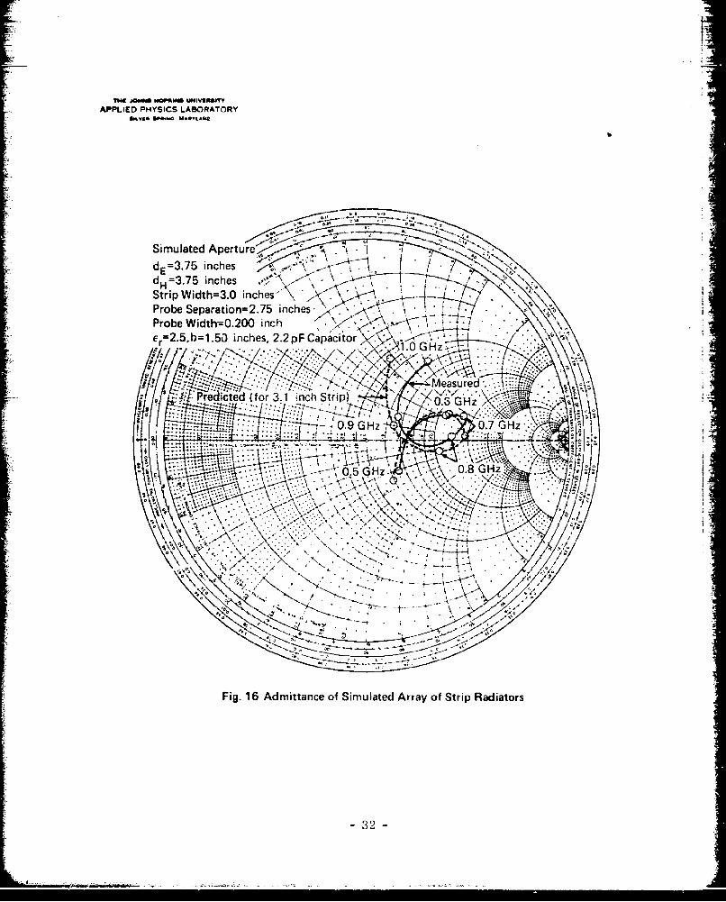
Octave band feed networks as described above, witha VSWR under 1.5:1 over the 0.5 to 1.0 GHz octave band,were built and incorporated in a simulated array. Figure 17is a photograph showing the aperture and feed network. Inthis array a lightweight dielectric (Eccofoam Hik 625D) with-r = 2. 5 was used. Otherwise the aperture was the same asabove. The feed networks used stripline construction, andthe extended center conductors of the outputs formed thefeed probes. Measured data on this aperture were nearlyidentical to those with each probe individually terminatedin 50 ohms.
-31-
INE JON"i NQPOUND U4IvCWrvAPPLIED PHYSICS LABORATORY
Simulated Apertured=.5inches
dH=3 .75 inches '.
Strip Width=3.0 inches\Probe Separation= 2.75 inchesProbe Width=0.200 inch
fr=.,=.t inches, 2. 2pF Capacitor ,>
I! ~ 7~K~. ~.4 , easu red A..~.? redicted (for 3.1 inch Strip) ,~
0. .z. G9
*...~~... '0G z0IT
-32-
fT JOHNS HOPKINS UNIVERSITYAPPLIED PHYSICS LABORATORY
33 -,
jT g Ap S HO tI OU417YIAPPUED PHYSI LABORATORY
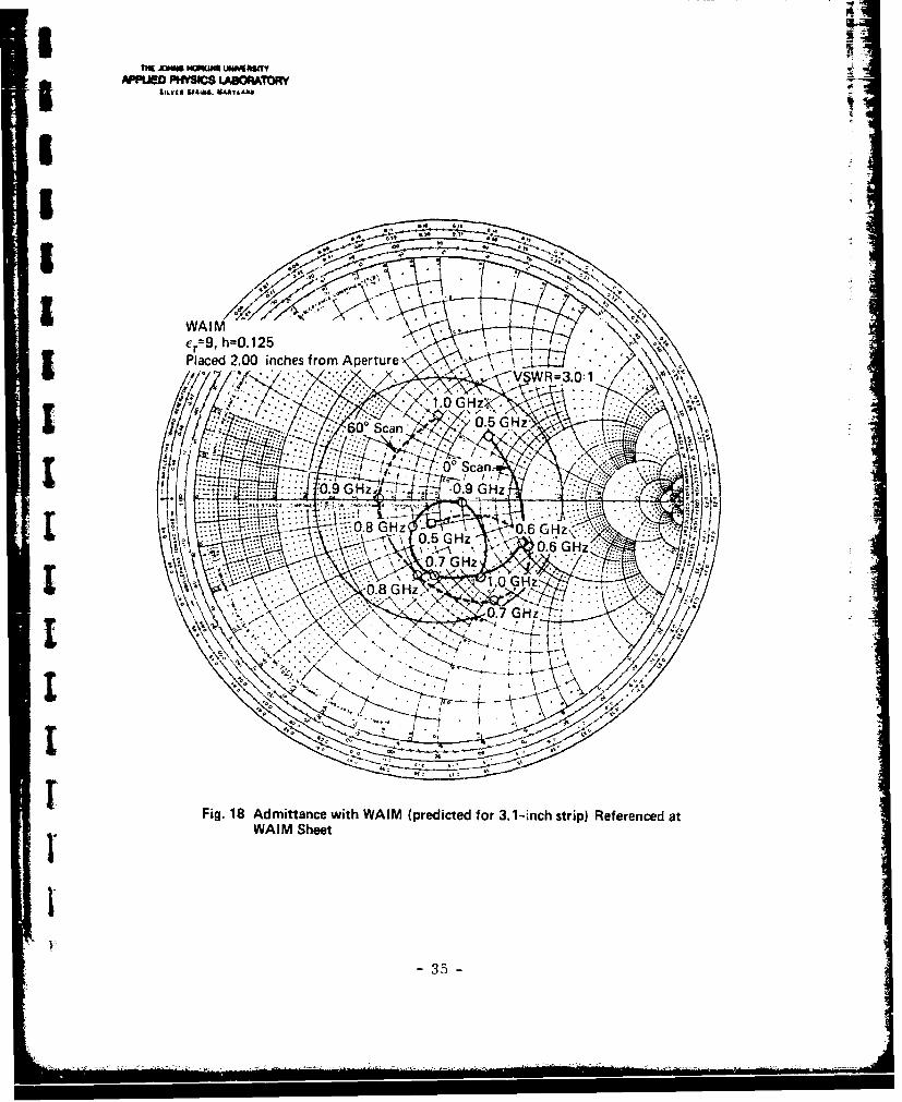
A final modification to the aperture was to use awide-angle impedance matching (WAIM) technique developedby McGill and Wheeler (Ref. 13) to improve scanningperformance. The technique uses a thin, planar, dielec-tric sheet with a high relative constant, that is as large asthe aperture and is placed in front of and parallel to thearray face. The admittance of the sheet is susceptive andis dependent on both scan angle and polarization. For athin dielectric sheet the susceptance at broadside is given by
B(0) 1 ) . (3)YO r
The susceptance variations with scan angle in the E- andH-planes are
B()_sin 28E-plane: B(0) cos 8 (4)B() cos O
r
B(O) IH-plane: B = Cos (
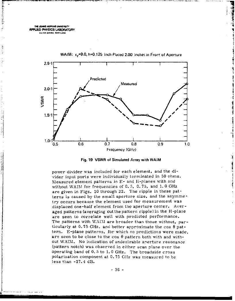
Referring to the Smith chart plot of calculated apertureadmittance (for a 3. 1-inch strip) given in Fig. 18, we cansee that a 0. 125-inch dielectric sheet with ir = 9, spaced2.00 inches in front of the aperture. can improve 11-planescan performance to a VSWR of less than 3.0:1 for scanning,to 600 over the 0.5 to 1.0 GHz band. VSWR measurementswith the WAIM on the aperture (trimmed to a 3. 0-inch stripwidth) were performed in a waveguide simulator with the re-sults shown in Fig. 19. The measured values correlatereasonably well with predicted values.
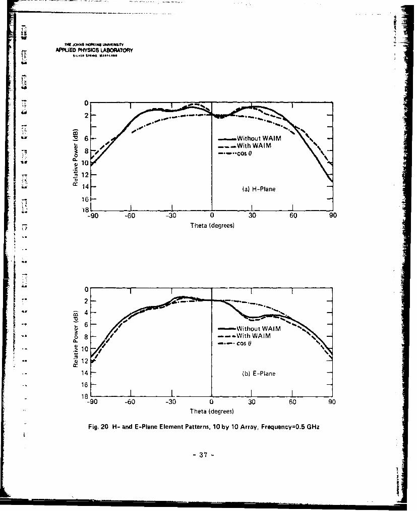
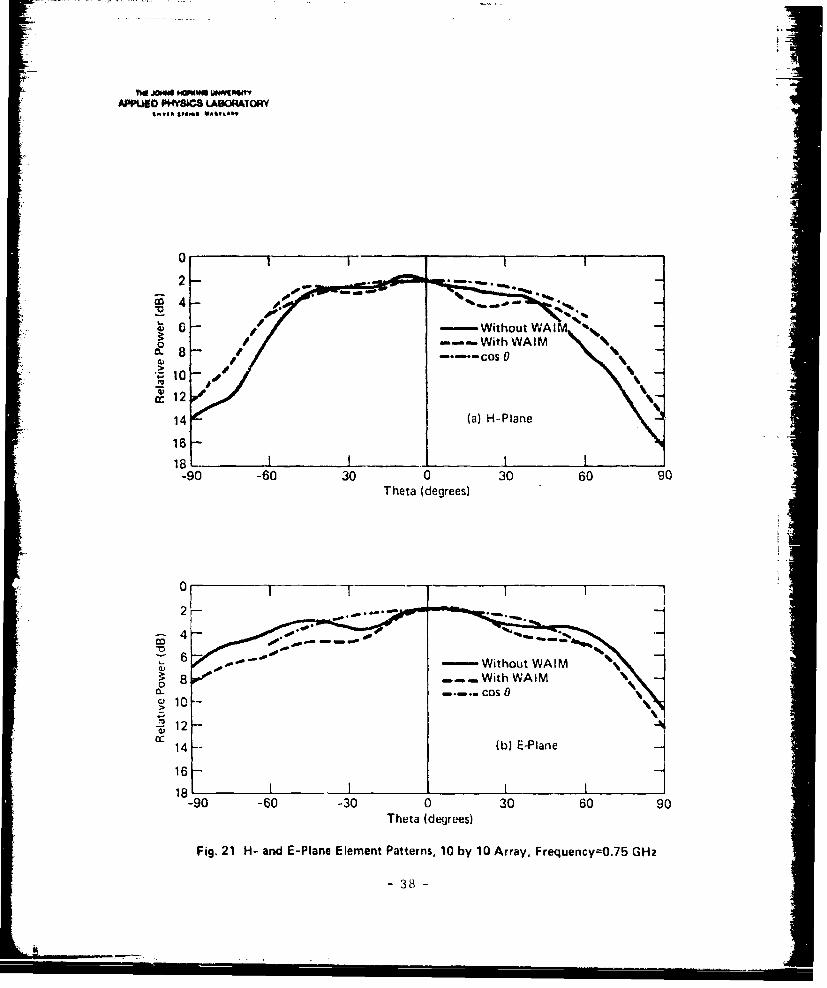
A 10- by 10-element array was constructed to mea-sure element patterns and thus to verify H-plane perfor-mance and observe E-plane characteristics. An antiphase
Ref. 13. E. G. Magill and H. A. Wheeler. "Wide-Angle Impedance Matching of a Phased Array Antenna bya Dielectric Sheet, " IEEE Transactions on Antennas andPropagation, Vol. AP-14. January 1966, pp. 49-53.
- 34 -
WAI~DPlarced 2.00inchAfo m prtr£ ZILV&E£I~Vs4 R=3 0:1
1. I.6'Scn5
.£0
O9Gz.,...J.9 GHz-
t -r~~~~ 0.5GHz 06H..
0.7 GH
I Fig. 18 Admittance with WAIM (predicted for 3.1-inch strip) Referenced atWAIM Sheet
-35
THE JOHN& HN9W4 UWiVEKtyAPPUED PHYSICS LABORATORY
IL, vli $Poo". NIN 4"lvt
WAIM: fr=9.0, h=0.125 inch Placed 2.00 inches in Front of Aperture
2.5:1 1 i 1 I
-- Predicted./ .Measured =
2.0,1
11.5:1 - . t-_
1 .o: I II0.5 0.6 0.7 0.8 0.9 1.0
Frequency (GHz)
Fig. 19 VSWR of Simulated Array with WAIM
power divider was included for each element, and the di-
vider input ports were individually terminated in 50 ohms.
Measured element patterns in E- and H-planes with and
without WAIXI for frequencies of 0. 5, 0. 75, and 1. 0 GHz
are given in Figs. 20 through 22. The ripple in these pat-
terns is caused by the small aperture size, and the asymme-
try occurs because the element used for measurement was
displaced one-half element from the aperture center. Aver-
aged patterns (averaging out the pattern ripple) in the H-plane
are seen to correlate well with predicted performance.The patterns with WAIM are broader than those without, par-ticularly at 0. 75 GHz. and better approximate the cos e pat-tern. E-plane patterns, for which no predictions were made,are seen to be close to the cos 0 pattern both with and with-out WAIM. No indication of undesirable a.nerture resonance
(pattern notch) was observed in either scan plane over theoperating band of 0.5 to 1. 0 GHz. The broadside crosspolarization component at 0. 75 GHz was measured to beless than -27.4 dB.
- 36 -
-- i -....... .... .... i . .. .. ...i .. .i ...
1wliE "CHW Mc.tUS uwiwty
AIVUED RMYS LAOATORY
2
(aOHPln
IM%0K0
12
cc 14 (a) E-Plane
1611 181II_ _ _ _ _ _ _ _ _ _ _ _ _ _ _ _
-90 -60 -30 0 30 60 90Theta (degrees)
8~ ~ ~ 37 --- ihWI
Cos 0
APPLIED PWfS4CS LABORATORYIst goal"B *4S1A*0
0
2%
-Without WAIMo / --- With WAIM
/ 9%10 -j .
I%cc 12 I
14 (a) H-Plane
181-90 -60 -30 0 30 09
Theta (degrees)
0
12
90 -60ou -30 30609
0- 3os 0
APPLIED PH{YSWC LAEOMLToR
0 %I1 2
-Without WAIM
CL 16
12J2 3 3 09
"pw
PIP Theta (degrees)
0I
~ 2
- -9 -- ihW I
____________________________COS ______
-APPLF PHYSICS LABORATORY" ., SpBILYIP S t.Mr. MAEq 'L AND
3. WIDEBAND TRANSISTOR POWER AMPLIFIERS
AMPLIFIER DESIGN METHOD
The RF generating sources for the experimentalsolid-state array are microwave transistor amplifiersoperated in the high efficiency class C mode. Operationin the class C mode has the unfortunate property of limit-ing instantaneous bandwidth in single transistor, amplifiersto less than an octave. Harmonic frequencies present inthe output waveform must be filtered by a less-than-octavepassband filter. The filter is normally inherent in the am-plifier output circuit.
Wideband class C power amplifiers at microwavefrequencies require design methods substantially differentfrom those used in small signal, class A designs. In smallsignal designs. "s"-parameter characterization is applica-ble, and the input and output impedance matching networkscan be considered jointly in meeting design objectives.Characterization by " -parameters is not applicable inclass C designs because of the nonlinear operation, and theinput and output networks must be considered separately.The output matching circuit is designed to achieve good ef-ficiency and saturated output power over the bandwidth.The output circuit also affects power gain, which is oftenin conflict with output power objectives, and significantlyaffects the amplifier input impedance. Input circuitry isprimarily directed at maximizing or lexeling the amplifiergain over the required bandwidth.
The output circuit is designed first in class C poweramplifiers with the objective of achieving a specified satu-rated output power at maximum efficiency. An approxima-tion for the required load conductance is arrived at by usingthe expression given in Appendix E (Eq. (E-5)) for saturatedoutput power:
1 GHF 2 cc sat L
- 40 -
TM XM4S HOMIN3 UWrASIIYAPPLIED PHYSICS LABORATORY
$ILVEM IMI G. MSI'LAND
The term Vsat is not a well defined quantity with microwavetransistors and must be determined experimentally. DC-RFefficiency is affected by the susceptance of the load and, fromAppendix E (Eq. (E-10)), is approximated by
f V cc~v sat 1+(BL/GL 2*
cc
Thus, the ranges over which the load conductance and sus-ceptance are allowed to vary for a given output power andefficiency specification can in principle be defined.
In reality the approximations of Eqs. (E-5) and(,--10) do not yield reliable results because of complexparasitics and an ill-defined threshold of saturation inmicrowave transistors. The experimental procedure indesigning an amplifier is to start with a load as determinedfrom the approximations and then to tune the load to achievethe desired power and maximum efficiency at several fre-quencies across the band. After the optimum loads at sev-eral frequencies across the band are found, an output cir-cuit is designed to approximate as closely as possible theoptimum load.
The input circuit is designed to impedance matchthe transistor with the transistor connpcted to the previ-ously designed output circuit since it affects the input im-pedance. Maximum gain with the given load results whenthe input is matched. If gain leveling is desired, selectivemismatching is designed into the circuit. The procedure
iL used in designing the input circuit is to impedance matchthe input with stub tuners at each of several frequencies
vacross the band while keeping the output power at the pre-scribed level. At each frequency, the input tuning is re-moved from the transistor, and its impedance is measured"looking back' from the transistor. The measured imped-ance is appropriately transformed to the transistor input.The input circuit is designed t2 approximate the trans-t' i formed optimum impedance across the frequer hand.
-41-
THE JOHN$ "OKI4NS UktYERIIAPPLIED PHYSICS LABORATORY
$Sibyls IpgrM .MAn.VA~tO
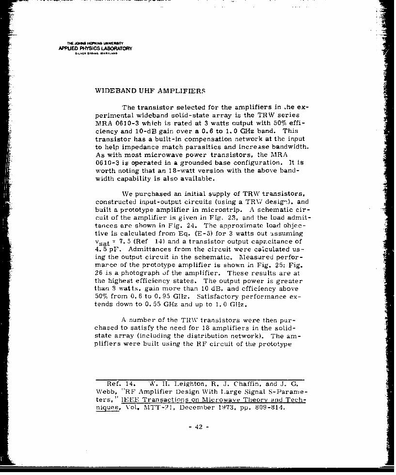
WIDEBAND UHF AMPLIFIERS
The transistor selected for the amplifiers in .he ex-perimental wideband solid-state array is the TRW seriesMRA 0610-3 which is rated at 3 watts output with 50% effi-ciency and 10-dB gain over a 0. 6 to 1. 0 GHz band. Thistransistor has a built-in compensation network at the inputto help impedance match parasitics and increase bandwidth.As with most microwave power transistors, the MRA0610-3 is operated in a grounded base configuration. It isworth noting that an 18-watt version with the above band-width capability is also available.
We purchased an initial supply of TRW transistors,constructed input-output circuits (using a TRW design), andbuilt a prototype amplifier in microstrip. A schematic cir-cuit of the amplifier is given in Fig. 23, and the load admit-tances are shown in Fig. 24. The approximate load objec-tive is calculated from Eq. (E-5) for 3 watts out assumingVsat : 7. 5 (Ref 14) and a transistor output capacitance of4. 5 pF. Admittances from the circuit were calculated us-ing the output circuit in the schematic. Measured perfor-marce of the prototype amplifier is shown in Fig. 25: Fig.26 is a photograph of the amplifier. These results are atthe highest efficiency states. The output power is greaterthan 3 watts, gain more than 10 dB. and efficiency above50% from 0. 6 to 0. 95 GHz. Satisfactory performance ex-tends down to 0. 55 GHz and up to 1. 0 GHz.
A number of the TRV transistors were then pur-chased to satisfy the need for 18 amplifiers in the solid-state array (including the distribution network). The am-plifiers were built using the RF circuit of the prototype
Ref. 14. W. I. Leighton, R. J. Chaffin, and J. G.Webb, "RF Amplifier Design With L.arge Signal S-Parame-ters." IEEE Transactions on Microwave Theory and Tech-n , Vol. MTT-:?. December 1973, pp. 809-814.
- 42 -

siifIFChk
I nput-e.-50' 9-'0 5-9- 50 12' 50'Y--m- Output
j4~Transistori'
O.056?X005) 0.175X 0.057X 0.153X 0.038XI X=-Wavelength at 0.8 GI-z
I Fig. 23 Schematic Circuit of the Prototype Amplifier
Aproimt Loa Obetve-
4-3
APPLIED PHYSICS LMBORY~AS&LVIN &PRO&. MAITLAND
6
5-
4
0
000
3
121
11
10
50
4 0 I0
444

AE W~i%% U4*f
APPUED PHYSICS LABORATORY
Fig.i 26a ThePrtoypeAmliie
pFig.r26 Th ProtoypAmplifier
with specially designed circuit frames. Figure 27 is a 5~photograph of a typical amplifier. The output circuit was
built on a 99. 5% alumina substrate I by 3 by 0. 025 incheswith a 0.000 010 inch surface finish. Conductor metalliza-
tion Is 0. 000 250 inch of gold on top of a chrome bondinglayer 10 nm thick. The input circuit was built on an iden-tical substrate 1 by 1 inch thick.
Measurements performed on the several amplifiers
showed performance that was significantly different fromthat obtained with the prototype; in all cases performancewas degraded. The difference is attributed to variationsin transistors from batch to batch and differences in pack-age parasitics possibly due to changes in fabricationmethods, personnel, or normal uncontrollable variationsin the fabrication process. Since the input-output circuits1were designed around the transistor used in the prototype,it is not surprising that performance was degraded in allothers.
-45-

1)4 JOHNU M~aI4 W4M Natty
APPLiED PIfYSC8 LADORATORY1g4v88 Ua.~ UA3w~Aao
*
I
ii ~
4I.
I 6
*.5C,,
(I
0I..S
.4-
4,' *5.
U.
C''I
64tWo I di
14
* 4
- 46 -
utomJED Krs LAOPATORYl $ Stves ulsaqdi. MaS-hfls
IDue to this degraded performance, it was necessary
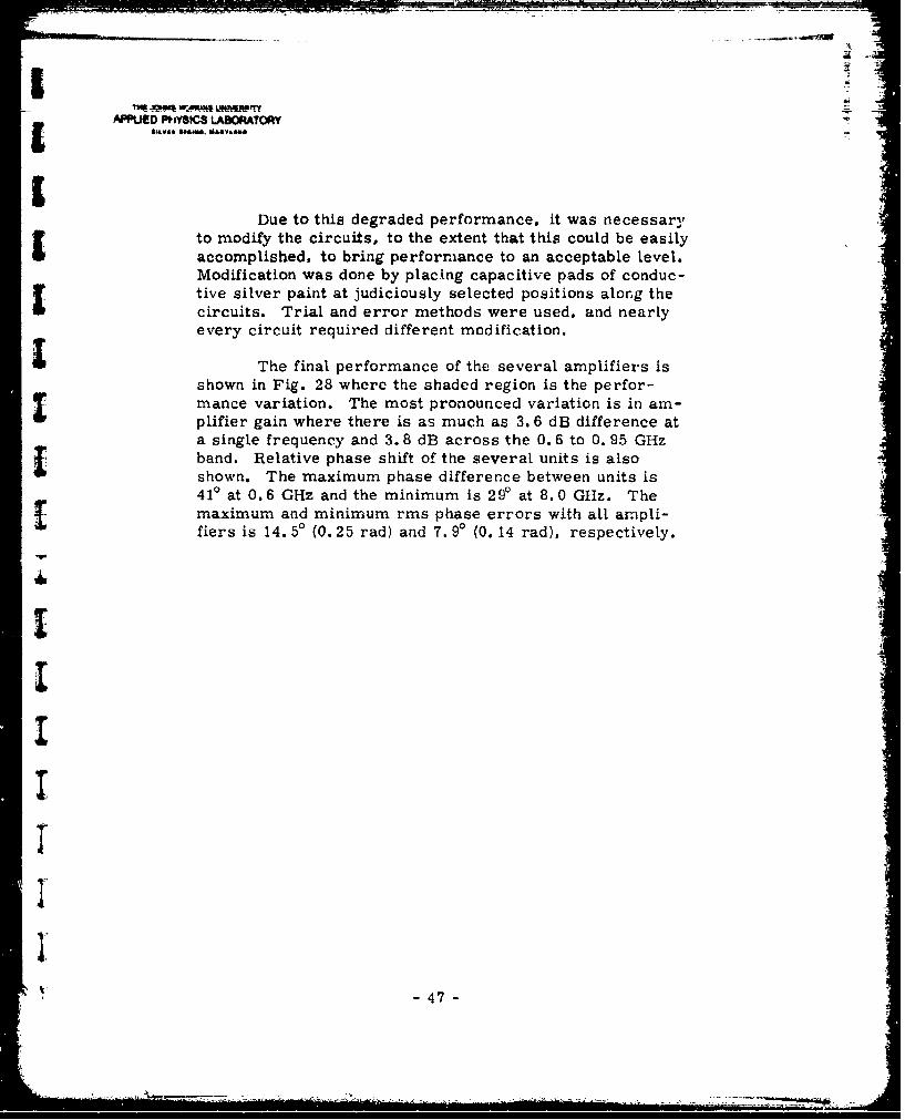
to modify the circuits, to the extent that this could be easilyaccomplished, to bring performance to an acceptable level.Modification was done by placing capacitive pads of conduc-tive silver paint at judiciously selected positions along thecircuits. Trial and error methods were used, and nearlyevery circuit required different modification.
IThe final performance of the several amplifiers isshown in Fig. 28 where the shaded region is the perfor-mance variation. The most pronounced variation is in am-plifier gain where there is as much as 3. 6 dB difference ata single frequency and 3. 8 dB across the 0. 6 to 0. 95 GHzband. Relative phase shift of the several units is alsoshown. The maximum phase difference between units is410 at 0.6 GHz and the minimum is 290 at 8.0 GHz. Themaximum and minimum rms phase errors with all ampli-fiers is 14. 50 (0. 25 rad) and 7. 90 (0. 14 rad). respectively.
I 4
II'I
t -47 -
- -
lIE0W MOIWE UWAFAWYAPPLIED PHfYSICS LABORATORY
Sts.vAR 3fIMI. WANTLAND
40 - Maximum Phase Difference
~30
S20 - rms Phas. Difference
10
11
.~10
c~ 9
8
7
6
S60
*~50
LU
240
30
20 I0.55 0.60 0.65 0.70 0.75 0.30 0.85 0.90 0.95
Frequency (GHz)
Fig. 28 Final Performance of the RIF Amplifiers
-48-

--
APPLUE PHYSICS LABORATORY
4. INTEGRATED ANTENNA SYSTEM
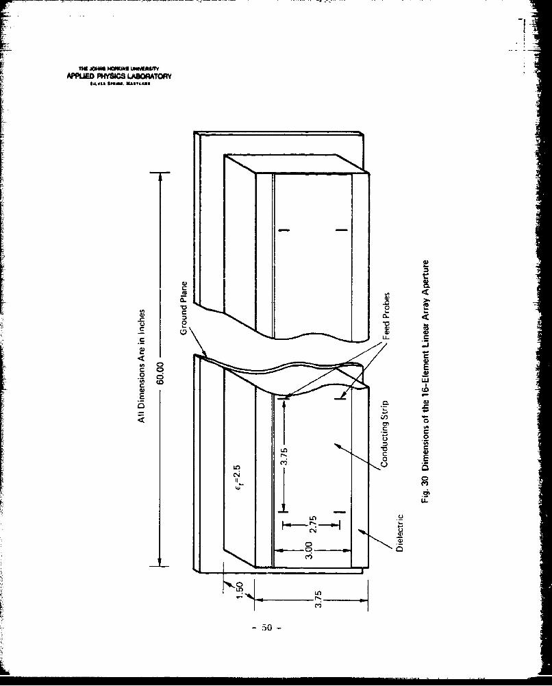
A 16-element linear array aperture of the printedcircuit radiators and several transistor amplifiers wereintegrated to form an array system with experimental verywideband solid-state characteristics- it is shown schemati-cally in Fig. 29. Dimensions of the aperture (without theWAIM sheet) are given in Fig. 30. Performance ohjectivewas beam scanning to 1600 in the H-plane over a 0.6 to0. 95 GHz band (the amplifiers capacity was the limiting
I factor).
Transistor8:1 Power Amplifier
Splitter Beam Steering 10-drb GainDelay Lines Circu'ator
Transistor E t V -Amplifier - -vv -v- -- v-- - ) . _A rr
rAperture
Splitter Circulator
.
4. Fig. 29 Schematic of the 16-Element Solid-State Array System
- 49 -
Li IL1)6JONS~WS ONG T
~.~II3 ~3OATCCI4&vI Lema MavE
.2[[ ____________E
1--
0
CC
CNC
Low
500
APPUED P94YSIC LABORATORY
A large planar array was simulated in the nonscan-ning E-plane (to maintain aperture impedance match) byplacing the linear array aperture between parallel conduct-ing planes spaced by the E-nlane element spacing of thesimulated array. Elements are imaged in the planes in afashion identical to that in a waveguide simulator. Theends of the array were closed off and the enclosure flared
V out into a horn for radiation into space. To minimize horn
aperture reflections (VSWR < 1.5:1), the E-dimension (24inches) of the horn was chosen to be greater than one wave-length at the lowest frequency. The E-plane horn angle of
,-- 230 minimizes horn throat reflection (VSWR < 1. 5:1). H-plane scanning to 600 required that the H-plane horn anglebe d600. Horizontal space limitations in the anechoic chain-ber used for the measurements forced the horn to be builtin two parts. A basic section was built with F300 H-planeflares permitting scanning to *30 . A wing extending oneside to 600 was attached for scanniag between 300 and 600.In the latter configuration, the array had to be set off-center on the chamber pedestal in order to be accommo-dated in the anechoic chamber, Figure 31 is a photographof the array system mounted on the pedestal in the chamber.
Each radiating element in the array was driven by
a 0. 6 to 0. 95 GHz bandwidth transistor amplifier. Theseveral amplifiers were arranged in the array accordingto gain such that. at midband. higher gain amplifiers werein the array center and lower gain units at the edges. Am-plifier gains vary with frequency as well as from unit tounit, resulting in the aperture amplitude errors given inFig. 32. The outputs of the amplifiers were protectedfrom aperture mismatch by isolators.
The distribution network for the experimental arraywas a matched 16:1 power divider assembled from 1800 hy-brids. This type of manifold provides isolated feeds to theRF drive amplifier at the elements, thus eliminating aper-ture illumination anomalies due to amplifier input mismatch(i.e., a reactive feed network has an output power distribu-tion strongly dependent on load mismatch). Two RF
- 51 -
APPtJIO FW6;GG. L*AjOAEy£r.<& OOM $ ~W. A.11"
Fig.31 6-Eemen InegrtedLiner AraySystm Muntd o
.00,
-4,IFig. 31 16- Element ertdLNuearraSytmMnedo
Fi.3 peruest i Ampue ari to ham e t mlfe an
f.52 G
..--
APPUID PHVI" LUflATORY
amplifiers were used within the feed network to supply RF
j power to the drive amplifiers.
Beam steering. confined to the H-plane, was ac-complished by inserting lengths of time-delaying coaxialcables between the feed network and integrated array ele-ments. Cable sets were procured for the scan angles ofOc . 150. 300. 45". and 600.
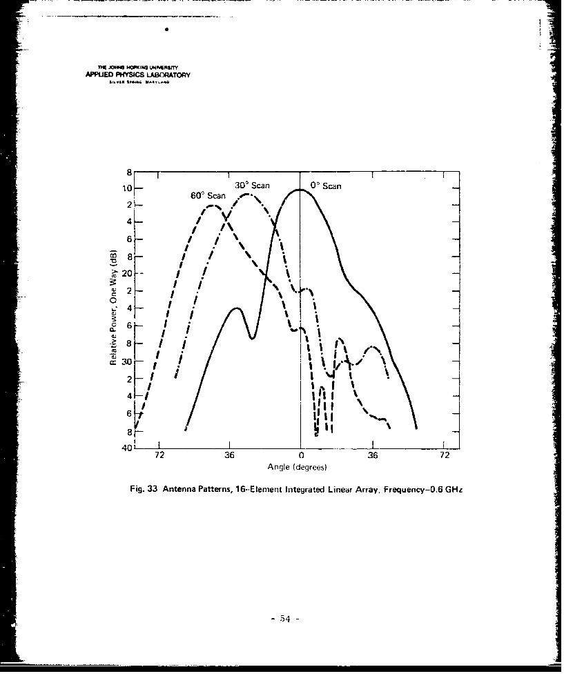
Antenna pattern measurements on the integratedarray were made in an anechoic chamber at the APL An-tenna and Boresite Facility. Patterns at 0. 6. 0. 75. and0.95 GHz for the H-plane scan angles of 00. 300. and 600are given in Figs. 33. 34. ard 35. The 0' and 30" beamsshow beam widths and sideiobe levels approximately as ex-
-- pected. The lack of sharp nulls between sidelobe is dueto phase error between driver amplifiers at each radiatingelemcnt. and is particularly pronounced at 0. 6 GHz wherethe maximum phase error exists. The asymmetry in thebroadside patterns is due to phase error between ampli-fiers with the two amplifiers in the feed distribution net-work probably contributing the most significant effect.
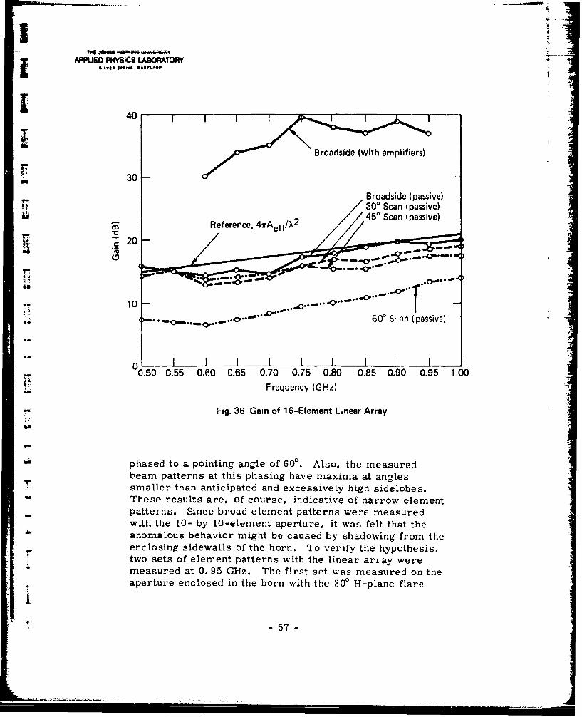
Measured antenna gain as a function of frequency isplotted in Fig. 36. Broadside gain is given for the solid-state array. and gain variation with scan angle is given forthe antenna without amplifiers (passive). The reference
- gain is for an assumed effective antenna aperture equal tothe array length (60 inches) times the enclosing horn height(24 inches). The observed rolloff in the broadside solid-state array gain at the high and low frequencies is due tovariation in transistor amplifier gains. As discussed pre-viously. the amplifier gains are maximum at midband androll off by as much as 3.8 dB at the band edges. In the ex-
t perimental solid-tate array the rolloff ; i approximatelytwice that of a single anplifier since the amplifiers in thedistribution network also have low gains at the band edges.
An unexpected result from the antenna measure-
ments is the low gain measured at 60: when the antenna is
- 53-
TH JHN m UNNERSMl
APPUED PHYSICS LABORAToRY
8 i
10- 30' Scan ' Scan
2 60' Scan
4- I /6-,
8-I• -k I *
> 20I-- I
0 I-a--'o 06- I
> 8 - / 1-, -4 -/ i i ' , ,,a: 30-
6 lII \8- 1
4072 36 0 36 72
Angle (degrees)
Fig. 33 Antenna Patterns, 16-Element Integrated Linear Array, Frequency=0.6 GHz
54-
"IHE ,4US mom" oIIVM4TYAPPUErI PHYSICS LAIORATORY
tAI
8 I0' Scan
10 60' Scan 300 Scan 0 Sa -
4I
g I
63
i 8 /
I - i I
> 20 g
2IC
o *
--55
0 4 -Tr/
2,
- 472 36 0 36 72
Angle (degrees)
Fig. 34 Antenna Patterns, 16-Element Integrated Linear Array, Frequency=O.75 GHz
-55-

TME JOHN" O" LOMPRATYAPPLIED P1-YfSC LABORATORY
SILVIA $95Im. AlAIVL*IO
8- 30' Scan 0' Scan
_ 10 - 60' Scan "'\
2
6 I I!~8
> 20
0 2 - I I I]
8 ( I0+I i • ',u
2 3o I i *iI i .
4: / iI 'J I I
- 56- -
2,-v "!!l -.i: (+ -l I 0
8 -
72 3003 7 z
F4g 35AtnaPten,-lmn nertdLna a, reqeny0.5
-66
l "I . . . ... .. .. . .. .. . .. .. .. .i :v-
WPULED PhftSICS LABORATORY
1r .
SILVIA |$"MSt. MANITLAWD[I'
~Broadside (with amplifiers)
30
RBroadside (passive)30' Scan (passive)
FReference, 4GrAeff/z2 4
T ~~~10- " """-, . --- o . , . . 0 • , , . • 6 0 ° S a n ( p a s s i v e )
00.50 0.55 0.60 0.65 0.70 0.75 0.80 0.85 0.90 0.95 1.00
~Frequency (G Hz)
- Fig. 36 Gain of 16-Element Linear Array
-" phased to a pointing angle of 600. Also, the measuredbeam patterns at this phasing have maxima at anglessmaller than anticipated and excessively high sidelobes.These results are, of course, indicative of narrow element
. patterns. Since broad element patterns were measuredwith the 10- by 10-element aperture, it was felt that theanomalous behavior might be caused by shadowing from theenclosing sidewalls of the horn. To verify the hypothesis.two sets of element patterns with the linear array weremeasured at 0. 95 GHz. The first set was measured on theaperture enclosed in the horn with the 300 H-plane flare
-57-
APPUEV F"YSC LA"ORY
8~WI Element No.f. 8
80 Element No.
2
4
6
~20
2I
30 i",
72 36 0 36 72Angle (degrees)
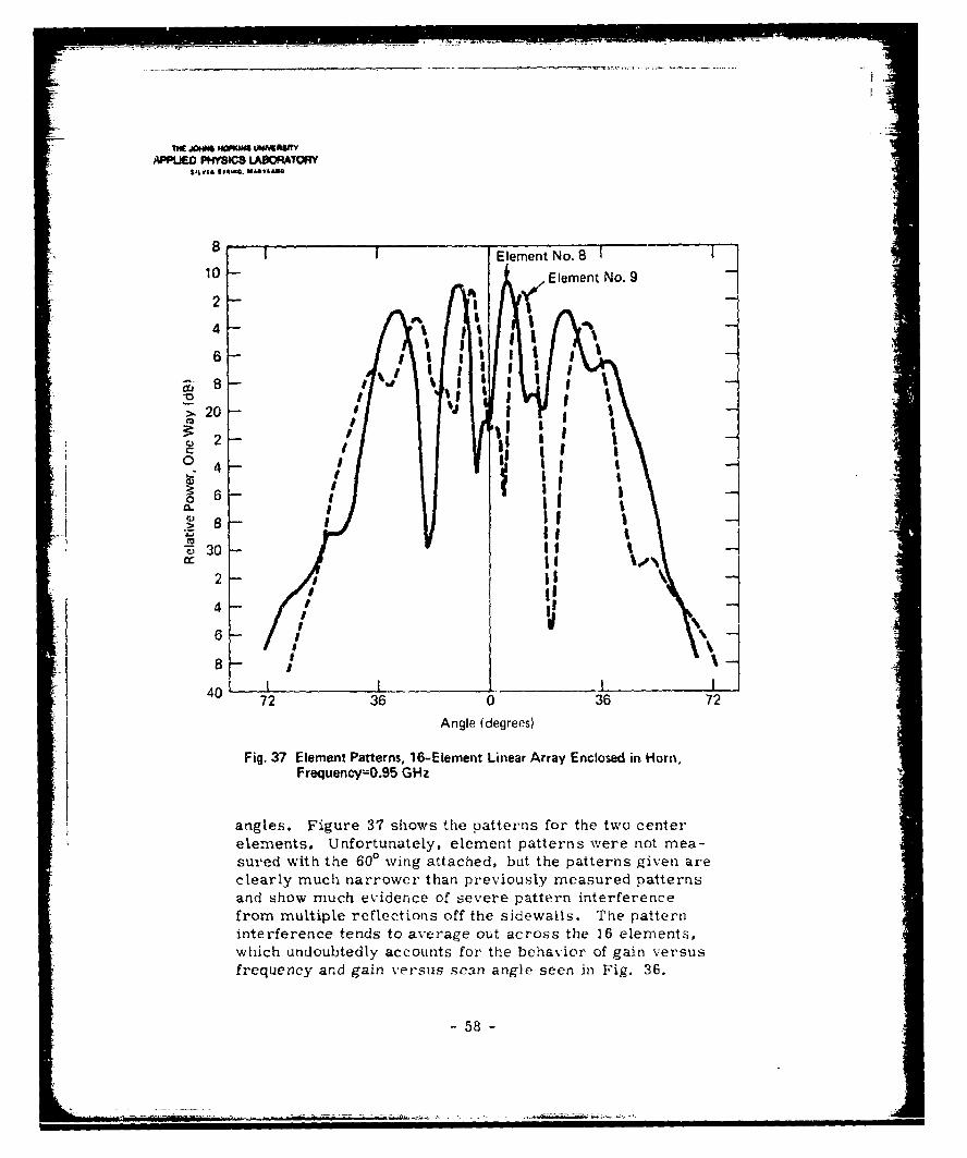
Fig. 37 Element Patterns, 16-Element Linear Array Enclosed in Horn,Frequency=0.95 GHz
angles. Figure 37 shows the patterns for the two centerelements. Unfortunately. element patterns were not mea-sured with the 600 wing attached, bUt the patterns given areclearly much narrower than previously measured patternsand show much evidence of severe pattern interferencefrom multiple reflections off the sidewallis. The patterninterference tends to average out across the 16 elements,which undoubtedly accounts for the behavior of gain versusfrequency and gain versus scan angle seen in Fig. 36.
-58
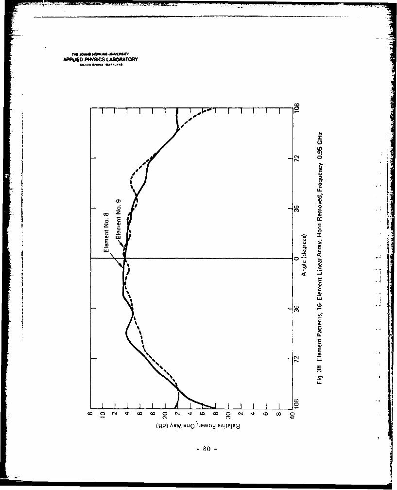
APP-ED PW LABORATORY -
The second set of patterns was measured with thehorn removed, leaving the array enclosed in a 9-in.ch sec-tion of parallel plane with small flare and open ends. Fig-
T ure 38 shows the patterns for the two center elements.These patterns are very broad, demonstrating that the hornenclosure is the cause of the narrow element patterns, low600 gain, and beam maxima occurring at small angles.
In conclusion, the experimental solid-state arrayhas beam steering capability to ±600. but the presence ofthe enclosing horn which was used to maintain apertureimpedance match caused the high scan angle beams to de-I teriorate. It shoulc be emphasized that the horn was ameasuring tool and would not be used in an operationalarray. Further, it is apparent from these observationsthat future experimental arrays of this nature should notbe enclosed in a horn but rather should be surrounded with
_ terminated dummy elements.
-59
II
II
-59-
APPLIED PHYSSCS LABORATORY
I4* J4p WAR'AI
N
C
A)
Cl00 z
EELu cu
E >Z
<
4m
CL
IE
S0 CN Iq w 0 (N v w. w 0 (N Iq wO w 0
(8p) AeM 9UQ 'JaMOd @A4ie@)
-60-

I__ o~HM"d UIMWfY
APPUED PHYSIC LAORTORY
5. SUMMARY AND CONCLUSIONS
We developed and tested a phased-array apertureimpedance matched over an octave bandwidth and with beam
f scanning to ±600. The aperture, consisting of strip radia-tors, was modeled, and design curves were ganerated. Pre-dicted performance of the aperture was a VSWR under 3. 0:1over a 0. 5 to 1. 0 GHz frequency band with scanning in theH-plane to 600. Experimental data from measurements ina waveguide simulator have demonstrated a close fit withpredicted data. A 10- by 10-element aperture was built tomeasure element patterns in the E- and H-planes; these pat-terns were close to the cos 6 shape out to 600 in both planesover the octave band. The aperture design is attractive forsolid-state array application in that it is made with printedcircuitry and lends itself to interfacing with integrated cir-cults.
Wideband transistor amplifiers, using TRW MRAb 0610-3 transistors operating in class C, were built and
evaluated for use as RF sources in a solid-state array.Performance of a prototype amplifier was greaterthan 10-d gain at more than 50% efficiency for powerpowelevels in excess of 3 watts over a 0. 6 to 0. 95 GHz band.When a large number (more than 18) of the amplifiers werebuilt, it was found that amplifier performance was signifi-cantly degraded due to variations in transistor character-istics. As a result none of the amplifiers achieved the per-
I formance of the prototype, and each amplifier had to beindividually tuned. This experience suggests that currenttransistor manufacturing methods are unable to mass pro-i duce transistors sufficiently similar for wideband high
power transistor circuits without individual tuning.
j A linear array aperture of the radiating elementswas integrated with the wideband transistor amplifiers toform a wideband solid-state phased-array systeia. Beamscanning, by means of inserting lengths of coaxial delay
-61-
L

--- '--I--
APPULD PMYSCS LASORTORY
lines between the antenna and a feed network, is to 600 inthe H-plane. Antenna performance was measured in ananechoic chamber over the 0. 6 to 0. 95 GHz frequency range(transistor amplifiers are the limiting factor). Satisfac-tory beam patterns were obtained for scan angles out to300, but patterns further out were less than satisfactorydue to pattern deterioration from the enclosing horn.
This developmental effort demonstrates that wide-band solid-state phased-arrays are feasible. Matched oc-tave band array apertures with wide angle scanning arewithin the current state of the art. Wideband transistoramplifiers are also available, but experience indicatesthat mass production is a problem. In addition, the ampli-fiers used in this effort are inherently limited to less thanan octave bandwidth (due to class C operation). A full oc-"ave, or greater, solid-state array would require furtherdevelopment in transistor amplifiers to achieve octave band-width circuits.
- 62 -
... ... ..... ... .., W A.,I !APPLED PWfS&CS LABORATORY3 II&VIR f)l 4Y AMS
Appendix A
EQUIVALENT CIRCUIT FOR ARRAY OF STRIPRADIATORS
The equivalent circuit for an array of strip radia-tors is developed from a model that considers the arrayaperture simulated in waveguide, as was shown in Fig. 3.The height of the waveguide simulator is one-half the E-plane spacing so that only a single feed probe of each ele-ment is included. However, multiple probes in the H-plane can be included. As described in the body of thetext, the model views the air-filled simulator and the aper-ture dielectric region as separate waveguide sections cou-pled by a slit. An array of feed probes excites fields inthe dielectric region (horizontal E-fields in Fig. 3). and as.ort circuited length of guide is paralleled across therobes. The slit coupled region, the array of feed probes.
and the short circuit guide section are treated separatelyin the following subsections: their equivalent circuits arethen joined to form the array aperture equivalent circuit.iz It is assumed that the separation between these waveguideobstacles is sufficient so that coupling by means of fringingfields between them is negligible.
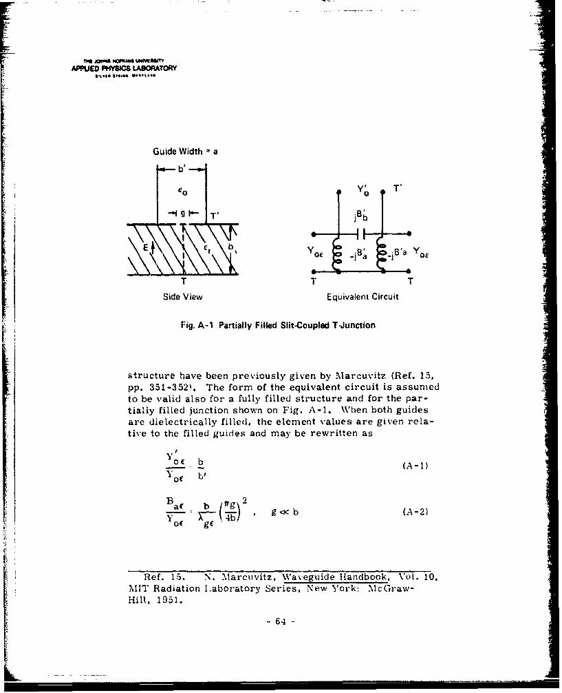
SLIT-COUPLED WAVEGUIDE SECTIONS
A portion of the strip radiator model consists oftwo waveguide sections coupled by a slit where one of theguides is filled with dielectric. The equivalent circuit ofthe coupling is developed by first considering the partiallyfilled T-junction shown in Fig. A-I. The two rectangularguides are of unequal heights but equal width, and are cou-pled by a narrow slit across a wall of zero thickness.TEl 0 modes are assumed to exist in both guides. The
[J equivalent circuit and element values for an air-filled
- 63 -
APPLIED P94YM*S LADORTORY
Guide Width a
b' T
E e b, y B'Of a 3B'a of~
T T T
Side View Equivalent Circuit
1:ig. A-1 Partially Filled Slit-Coupled T-Junction
structure have been previously given by 'Marcuvitz (Ref. 15,pp. 351-352). The form of the equivalent circuit is assumnedto be valid also for a fully filled structure and for the par-tially filled junction shown on Fig. A-1. WVhen both guidesare dielectrically filled. the element values are given reLa-tive to the filled guides and may be rewvritten as
b (A-1)
B ac b7). gxbg (A-2)
O(I g(
Ref. 15. N. 'MarcuitZ, %Vaveguide Handbook, Vol. 10.MIT Radiation Laboratory Series, New York: McGraw-Hill, 1951.
-64-
IB2 In + b << (A-3)
where o
" X 'I / ( -(X / ,c )2
46 To develop the equivalent circuit values 1,r the par-tially filled T-junction, it is necessary to cunsider sepa-rately the small slit or symmetrical iris across a rectangu-di ar guide. The iris is represented by a capacitive suscep-tance (Ref. 15. pp. 218-219). As before, when the guide is
dielectrically filled, the susceptance may be rewritten as
B cc 4 4b' 1b g2 I X •g 6 2b' 2 2b'
Of gf gl(I g<
(A-4)
where
X is replaced by X7g for air filled.
YI is replaced by Y
i'he equivalent circuit and element values of the par-
tially filled T-junction can now be found from the completelyfilled T-junction and the symmetrical iris. The couplingslit between guides in the partially filled T-junction is as-sumed to be narrow so that in the plane of the slit only hori-zontal field components normal to the strip edges exist.Under this assumption the guide section above the referenceplane T' is equivalent to one side of an air-filled guide withiris. It follows that the inductive components of the T-junction circuit are functions of the configuration below thereference plane and are unaffected by a change of dielectric
"* - 65-
f At M- -WNMv
APPUED P9'YS4S LABORATORY
L4-* J. 4:lA
in the upper region. The total capacitance in the partiallyfilled junction is arrived at by subtracting one-half thecapacitance of a dielectric-filled guide with an iris fromthe capacitance of a fully filled T-junction, and adding one-half the capacitance of an air-filled guide with an iris:
/ :1 + IBb Bb 2 B-1- -Bc (A-5)
B' I Y
I
b b 1c- (A-6)Yoc Yo0 2 y 0o YoI 2 Yo Yof'
where
B' = B anda aC
y ,o b g
"x ( 9
The junction of particular interest in modeling thearray aperture of strip radiators is the bifurcated T-junc-tion wherein only one-half of the above structure is con-sidered. When the T-junction is excited by a TE 1 0 modein the vertical guide, a conducting septum may be insertedalong symmetry plane T. as illustrated in Fig. A-2. Sincethe septum is normal to all horizontal fields, and at theplane of symmetry there are no vertical fields, the overallfield configuration is undisturbed. The resulting two L-junctions are separable, and each has the equivalent cir-cuit shown. Circuit values are given by
B 2B' (A-7a)g b
- 66 -
IIp
T unE Con dutn E o EL-Junions
0 9/20
7 bb
E Codctn E frE
E~ fr E E ET TT
T-Junction, Pair of L-Junctions,Side View Side View
I 2Y 10- T ***~~a
T' TEquivalent Circuit,
L-Junction
-I
i Fig. A-2 Bifurcated T-Junction
!I" t -67-
~f
THE JOW4 HOWNS UNWAM"1APPLED PHYSICS LABORATORY
SILVS* SPARCG hMACLARQ
_ 1 . ( _L a
YeA g Tr f 2 1 g; 12 2b'
(YT 1(24)1 (2~ W ) f (T~j
gg)
(A -7b)
B \2a.y \4b g << b (A-8)OC ge
GRATING OF METALLIC POSTS
The equivalent circuit of the feed probes is arrivedat by considering a planar grating of metallic posts andclosely spaced resistors in Lree space as depicted inFig. A-3. Axes of the posts are parallel to the electricfield of an incident plane wave arriving at angle 0. Theequivalent circuit for a grating of posts has been derivedby Marcuvitz (Ref. 15. pp. 285-289) (as in the figure, butwithout the resistors). When the radiating medium is dielec-tric rather than free space, appropriate substitutions in theelement values can be made, and the circuit values for thegrating of posts may be written as
X a aCos (3 1, (os) 2 C),_) /
-- 0,601 3 - 2 , a<< 1
- 68 -
ThE JC* O49 KI P O U!( N L WENSTYjAPPLIED PHYSICS LBRTR
Kit.Ef Simuato Walls
E IT- I
Ic!"
R RI- b bd'
El - 0
AAT- T
Equivalent Circuit
Fig. A-3 Grating of Posts with Series Resistors
-69-

TlE 9OS HOPK0,, UW IV ,TYAPPLED PHYSICS LABORATORY
X a aCos8 i 1E a
-n a ) + ( 1 4 . 5 1 3 c o s 6 a / k 3
a/X 0.5 (A-10)
X bE a cos 2ff r 2
Z ( a)(A-i)
where
2r ° d, 2r d for circular cross section - case a,
2r = d'/2, r 0 for coplanar ribbon posts - case b,and
2r d"/2, 2r 1 d" /2 for ribbon posts perpendicu-lar to grating plane -case c.
Equation (A-10) is obtained from fitting a curve to Marcu-vitz's plots for the complete expression. The equivalentradii for cases b and c are for rectangular posts with onedimension net to zero.
If small resistors are placed close together and inseries in each of the posts, the previous equivalent circuitis adapted to include a resistive component (Fig. A-3).The resistive component has the value r - R" a/1 expressedin ohms per square, and can be understood by consideringa square with sides D Nvhere nL ma - D. For con-venience let D take any value such that n and m are integers.In the D by 1) square there are m columns of resistorswhere each column has n resistors in series, resulting in
a total resistance for the square of 1 (nR) ohms or r R--Rm m
ohms per square. Since, from the above. nk= ma, it canbe seen that r = R a/L ohms per square.
A pair of vertical conducting walls may be inserted
that are normal to and pass through the grating to form an
- 70 -
APPLED PHYSIC8 LABORATORY
infinitely high waveguide. In the waveguide region planewave propagation is simulated at some incident angle. Thewalls must pass either through the axis of the posts ormidway between the posts to maintain the simulation. Hori-zontal top and bottom walls can be included in symmetryplanes, leaving the contained fields undisturbed. If the smallresistors are replaced by coaxial terminations at one hori-zontal wall, then the simulated array of posts is identical
, -~to the feed probes with the equivalent circuit shown and theimpedances of Eqs. (A-9), (A-10). and (A-11) wherer RBILr = R -A expressed in ohms for the A by B simulator
section. Here R is equal to twice the coaxial termination.
APERTURE EQUIVALENT CIRCUIT
A simulated array of strip radiators, shown earlierin Fig. 3. has the equivalent circuit given in Fig. A-4 foreach half-unit cell. R. is the coaxial termination of eachfeed probe. The circuit is formed by combining the cir-cuits of the L-junction and the feed probes. The sLit-coupled L-junction and feed probes are separated by a
I 'length (dE - s)/2 (characteristic impedance Zo) with ashort-circuited length of guide shunted across the probes.Circuit values, nr-_malized to guide impedances, are de-rived as previously discussed.
- dE s 2 -- If X-3-X
Zfs j81 2
Fig. A-4 Equivalent Circuit, Array of Strip Radiators (H-plane scan)
- 71 -
WPUEO PWSICS LAOATOAY
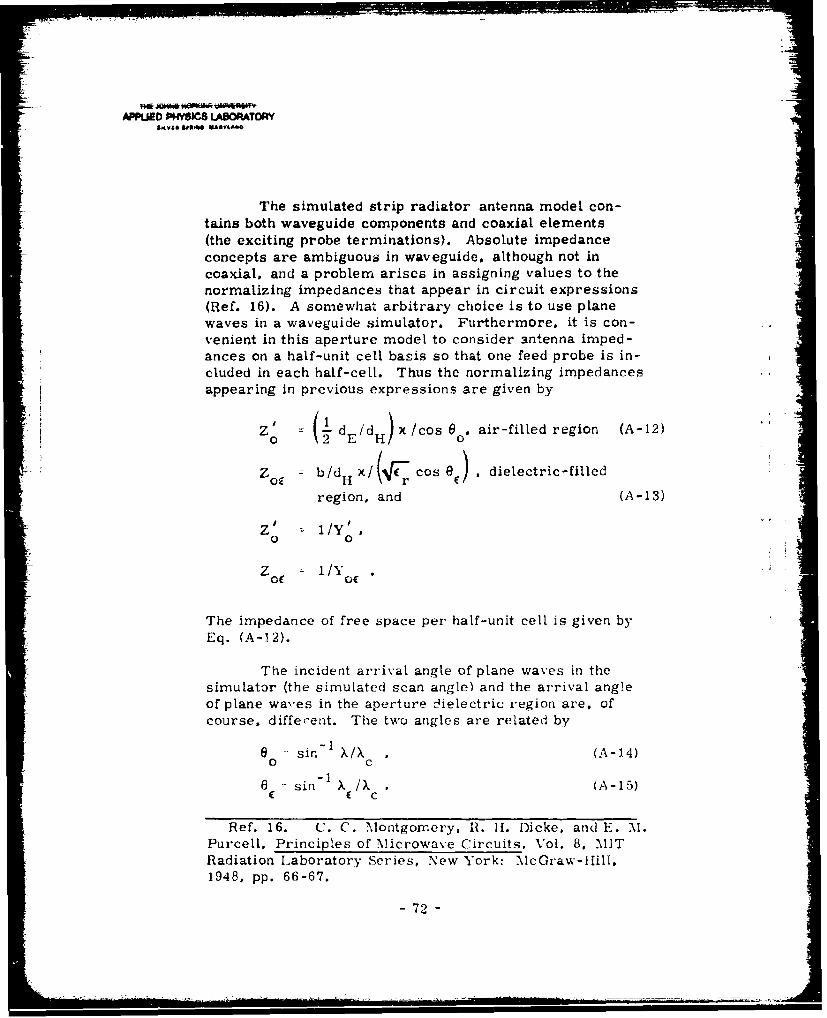
The simulated strip radiator antenna model con-tains both waveguide components and coaxial elements(the exciting probe terminations). Absolute impedanceconcepts are ambiguous in waveguide, although not incoaxial, and a problem arises in assigning values to thenormalizing impedances that appear in circuit expressions(Ref. 16). A somewhat arbitrary choice is to use planewaves in a waveguide simulator. Furthermore, it is con-venient in this aperture model to consider antenna imped-ances on a half-unit cell basis so that one feed probe is in-cluded in each half-cell. Thus the normalizing impedancesappearing in previous expressions are given by
Z' (1dE/dH) 0o , air-filled region (A-12)"0 2 o d- X/cos e
Z b/dH Xi(JF cos 19, dielectric-filled
region, and (A-13)
0 0
o oc.
The impedance of free space per half-unit cell is given byEq. (A-12).
The incident arrival angle of plane waves in thesimulator (the simulated scan angle) and the arrival angleof plane waves in the aperture dielectric region are, of
course, differ'ent. The two angles are related by
60 sin -1 Xc * (A- 14)
= C sin I X. /X c (A-15)C ( C
Ref. 16. C. C. "Montgomery, I. It. Dicke, and E. M.Purcell, Principles of Microwave Circuits, Vol. 8, MIT
Radiation Laboratory Series, New York: McGraw-Ifill,1948, pp. 66-67.
- 72 -

.2 -.
APPLIED PH{YS=C LASORTORY5 £LVI* Met". ATY&A
resulting in
sin0 sin8 , (A-16)I o| -r
where
I Thus, the H-plane scanning model of an array ofstrip radiators, which is identical to that of the simulatedaperture, has absolute circuit values referenced to a half-1 A unit cell as written below. The previously derived circuitvalues have been denormalized using Eqs. (A-12) and (A-13),referenced to the H-plane scan angle through Eq. (A-16),*5 and rewritten for convenience in the following equations interms of strip width.
I d H Cr sin a 2b d I d 12
( n2 2 ( [
r 0
(2[ ( )(E 2S+ ( Cr - sin ' o2(" " 14 1 d( L
1 -sin 2 8 2 ) 2+ ir -in 1 _ I -E -
C - si,-n , 2 e 1 - . -d- E ) 12, - --(
d[_I dF 2 2P cr - sin 2o' a 2 - w2
LI4- 73 -
ro ANSi W O JM W fvt.
APPLED PHWSI LABOAOR
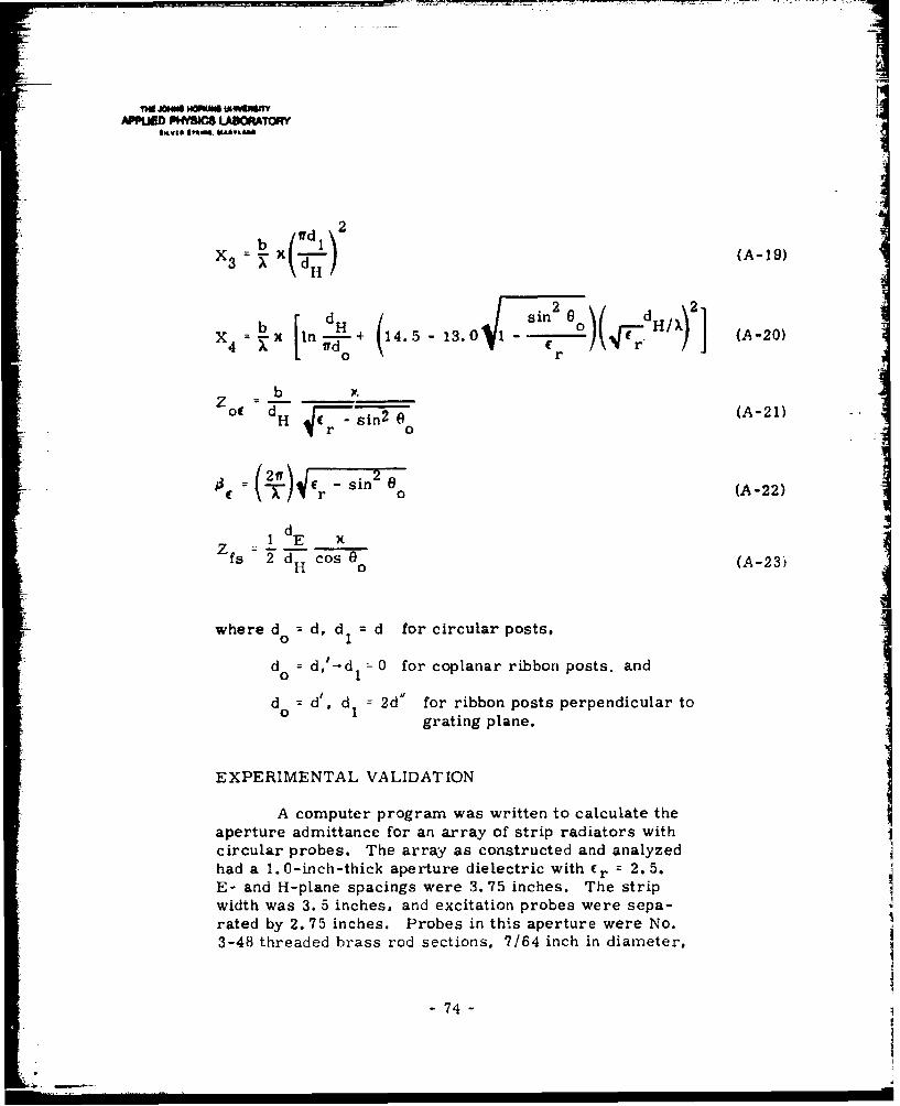
b ( (A-19)
d sin2 - d
r d )( (A-20)-X- 1 nH+14.5- 13.01-(2)4 0'd
d dH 4 7 sin2 0 (A-21)
=r 0~)Jiw (A-22)
d
fs 2 d H cos a (A-23)
where d = d, d = d for circular posts.
do d, --d 1 0 for coplanar ribbon posts, and
d = d' d 1 2d" for ribbon posts perpendicular tograting plane.
EXPERIMENTAL VALIDATION
A computer program was written to calculate theaperture admittance for an array of strip radiators withcircular probes. The array as constructed and analyzedhad a 1. 0-inch-thick aperture dielectric with ( r = 2. 5.E- and H-plane spacings were 3. 75 inches. The stripwidth was 3. 5 inches, and excitation probes were sepa-rated by 2.75 inches. Probes in this aperture were No.3-48 threaded brass rod sections, 7/64 inch in diameter.
-74-
APPUED PhfSICS LASORATORY
screwed into tapped solder cups of type N connectors. Theprobe diameter was taken as 0. 100 inch for the calcula-tions.
Admittance measurements were performed in awaveguide simulator with E- and H-dimensions of 7. 5 and15. 0 inches, respectively. Eight array elements were in-cluded in the simulation. Each element probe was termi-nated in 50 ohms. Predicted and measured admittancepoints over the frequency band of 0. 5 to 1. 0 GHz are shownon the Smith chart in Fig. A-5. Measured and predictedvalues are seen to be very close where the measuredvalues are slightly more capacitive than calculated.
77Z7
xu
- I
Sirr
U.
- 75 -
YHg -DW 000PRO WOUVtA4TV
APKMDC P,4YSICS LADDRATORY
dH=3 .7 5 inches ~.Cr=2.5,bl1.O inchStrip Width=3 5 inches ~ 0.9 GHz-260Probe Separation=2,75 inches 'IGH-3Probe Diameterz0 100 inch
08dGHz 29~$j
4 / i -~--~---Predicted.-
7 0.-a-Measured~
76
• = -- .... . .,.- ,
-!IAPPL.D PHYSS LADORATO
41. W al I lkvik. L'41
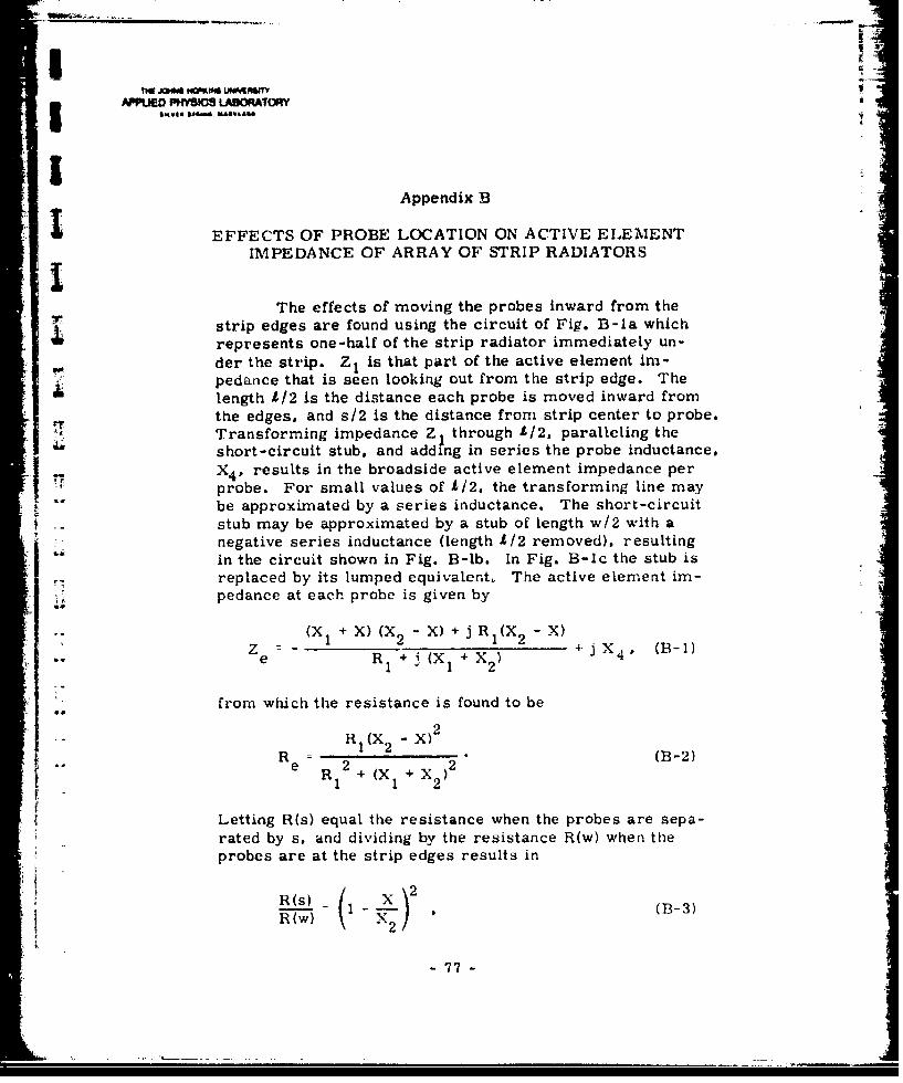
IAppendix B
EFFECTS OF PROBE LOCATION ON ACTIVE ELEMENTIMPEDANCE OF ARRAY OF STRIP RADIATORSI
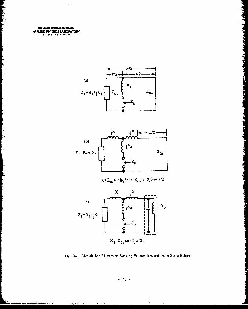
The effects of moving the probes inward from thestrip edges are found using the circuit of Fig. B-la whichrepresents one-half of the strip radiator immediately un-
der the strip. Z 1 is that part of the active element im-pedance that is seen looking out from the strip edge. Thelength 1/2 is the distance each probe is moved inward fromthe edges, and s/2 is the distance from strip center to probe.Transforming impedance Z I through A12, paralleling theshort-circuit stub, and adding in series the probe inductance.
X4 . results in the broadside active element impedance perprobe. For small values of 1/2. the transforming line maybe approximated by a series inductance. The short-circuitstub may be approximated by a stub of Length w/2 with anegative series inductance (length A/2 removed), resultingin the circuit shown in Fig. B-lb. In Fig. B-Ic the stub isreplaced by its lumped equivalent. The active element im-
i -pedance at each probe is given by
(X + X) (X2 X) + j R (X -X)Z 1 2- 1 2 jX 4 (B-i)
e R + (X + X21 1 2
from which the resistance is found to be
R (X -X) 2
121-- eR 12+Z 1 +X1 (B-2)
Letting R(s) equal the resistance when the probes are sepa-rated by s. and dividing by the resistance R(w) when theprobes are at the strip edges results in
-sj -i * (B-3)
- 77 -
APPLIED PHYS4S LABORATORY
(a)iX4
Z, =Rl+ xi ZoeZO
(b)
Z1 =R + x IZo
X . a hW) O ao (w-s) 2
4 c)
X =Z0(tan(o3 W/2)
Fig. B-1 Circuit for Effects of Moving Probes Inward from Strip Edges
-78-
a -.i
I BIM Awe IOW'*O UMAGMS
or
R~) tan ( 1/2)R (s) ca ( w (B-4)
-Approximating for smallA( 1/ 2 and letting 12 (w -s)/ 2results in
R~~s (- S/W) 8 w/22
- R~w)tan(#~ c/2))(B)
-79-
APULED PHYS= LAORA
Appendix C
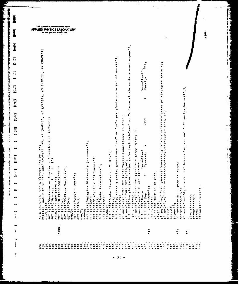
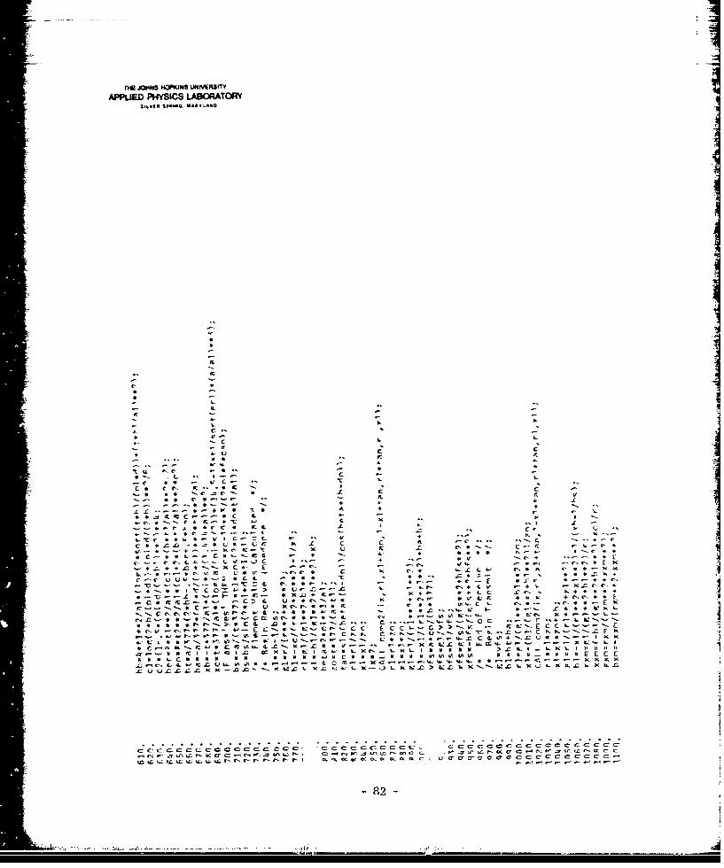
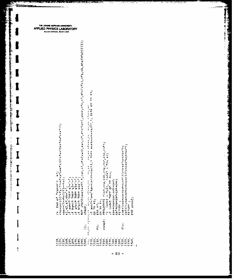
COMPUTER PROGRAM LISTING (CPS LANGUAGE)FOR STRIP RADIATOR ANALYSIS
The computer program listing for strip radiatoranalysis, in Conversational Program System (CPS) lan-guage, is given in the following pages.
- 80 -
IL
ILI
r- aC - t
3- C. a
a atuv
C- Cc -
I 6.- -
- bC C
d, w - C- - - -1* t : t :c s
ccc C CCC
c. Ic c 2 Ij . .% # m a C C :k C41 4 4r
fr81
APPLIED PHYSICS LABORATORY
att
U! V .4 f
4-~ -C S
W4- C- C* C In at
o- I-
cf x - I' >b C x 4+
4- -1 :z zC C c; z ) zC l ; c C zl ! c C c C ;C 7 C 7
- wt 4. c K
~ U It *-.c * K c-. '-LC CCK C8-2
APPLIED PHYSICS LABORATORY3 ~Si&ai Sf4550 M0SL&UM
1.1 -
C.
.4-
a L
Ii1 I iiv'A6. A A sir ( c c
* - -c Sc. :
E E SC C -a-
* . xzX C -C
C. -4m t 'CZ7c S CUa> CL c z uuaUL .
* - - C C
-a.. a ec83
TE JOW" NUIR WEIM1VAPPUED PHYSICS LABORATORY
IILV9t S#5M .MWA*YLkJi
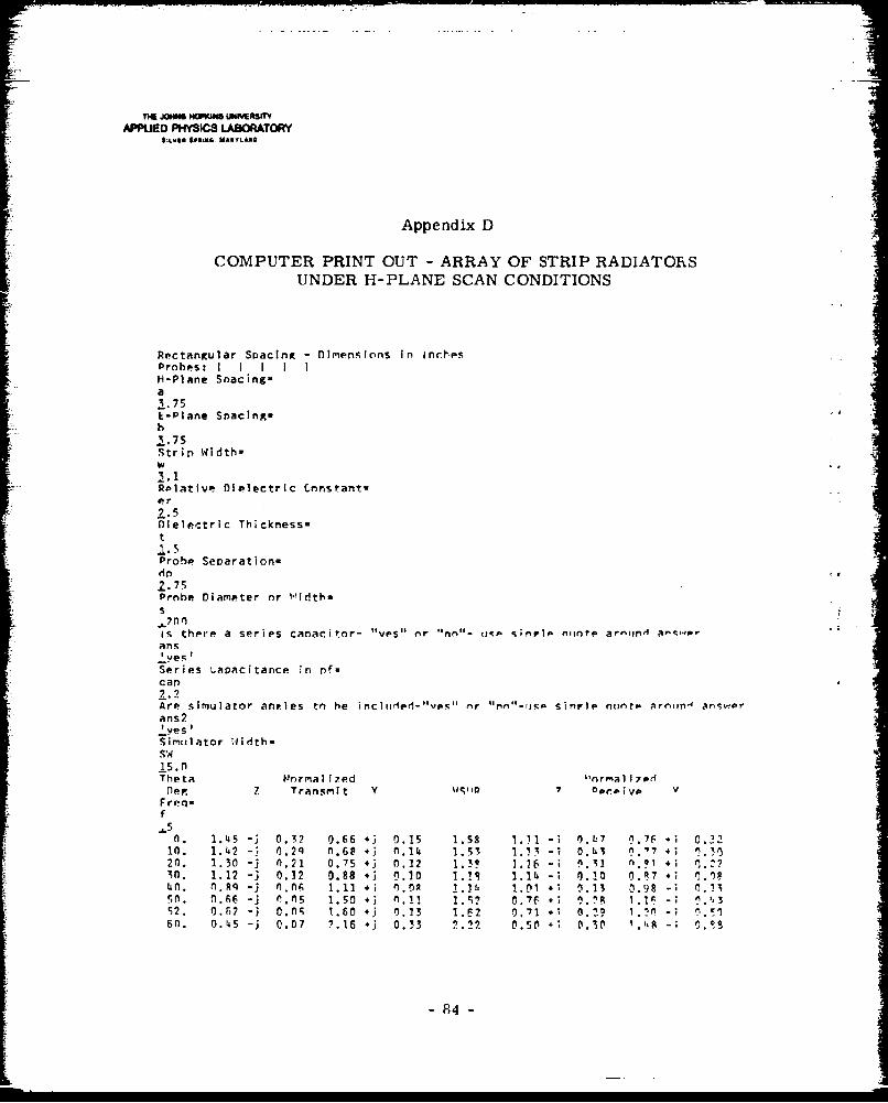
Appendix D
COMPUTER PRINT OUT - ARRAY OF STRIP RADIATORSUNDER H-PLANE SCAN CONDITIONS
Rectangular Snaclnz - Dimensions in inrhpsProbes: I I I I IH-Plane Snacing-a
E-Plane Spacing-b
4.75strip width-w
Relative_ Dielectric Constantser2.5Dielectric Thickness-t
Probe SeDarat ion-dn
s 2.75Prohe Diameter or 1'1idth.s
is. there a series canacitor-
Itvpsl " r nn"tl- tj-;A sinrflp niltp' aeClilA ,.
Series uaDacitance in pf.cap2
Are simulator an.les tn he incluld- "vP" or "oO"-iA Sini SAt,,, SipeI ar"rnI4 a we!r
ans 2"yes o
simulator Width-SW15. nTheta In rmalizpd "orMa1 i7pdDer 7 Tran.mit Yfg 7 Op .piVp v
Freq-f,.5
0. 1.L5 - 0.3? 0.66 .3 0.15 1.58 1.i -; 0.117 .7F 4 0 .3210. 1.42 0- ,.2q n.68 +j M 14 1.53 !.1. -; O.L3 6.77 1 . 3020. 1.30 -j n.21 0.75 *j 0.12 1.3 _ $ - .nn31 .; (1.2'in. 1.12 -j 0.12 0.88 +j n.10 ..l i 1" -; 0.10 0.17 .; 0.1840. n.fq -i n.06 1.11 41 0n.n i.1h I. n! 0.I 0.98 -i 0.ilnf 0.R6 -j n.n5 1.50 M 0.11 1.57 0."f6 +; !.0R I.1 -; .',3
52. 0.2 - 0.0 1.60 *j 0.13 1.52 0.71 .; 0.29 1.10 -; ).6n. -j 0.07 2.16 4i 0.33 ?.22 0.50 +; 0.30 .Its -; 09
- 84 -
I
APPIED PHYSICS LAMORATORY3 Ssa I PaWJ MA,*VLA**
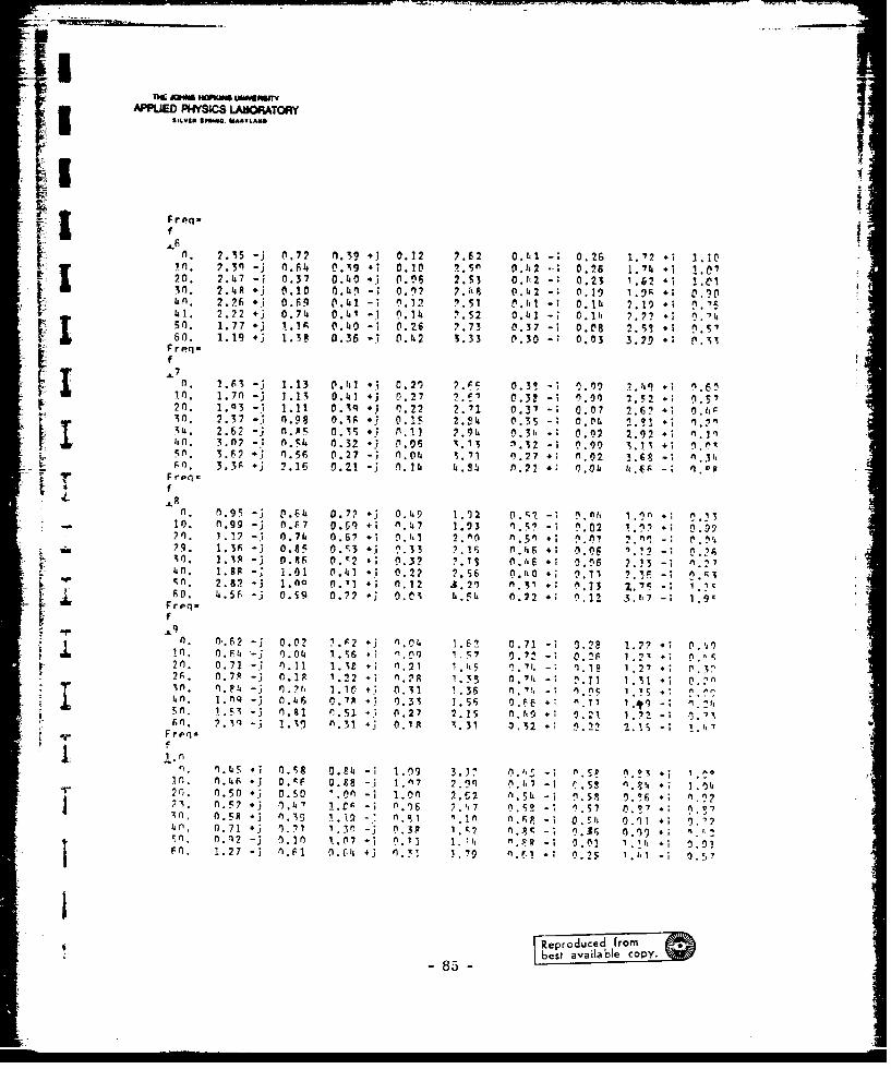
Freqs
Li 'sn. 2.15 -j 0.77 0.5 *j 0.12 2.62 0.1 -; 0.26 1.7? *; 1.10in. 2.3q -) ().F4 0.19 #i 0.10
1 2.5
n 0 .h2 -; ?S 1.74h *; 1.07
20. 2.4.7 -j 0.37 0.40 *j 0.CI6 2.53 0.h,2 -; 0.23 1.62 ,4; 1.tl
311. 2.42 -j 0.10 0.p -; n.9 ? 7.,9 0.32 -; .9 2.9 0.1 0n. 2. 26 +j 0.S. 0.41 = M.22 ? 51 0.1 -; 0 .1; . 16[,1. 2.22 *] 0.74 0.41 -j .14 7.52 0.t1 - 0.11) 7.2? 1. ,14
S•5n. 1.77 * 1..1A 0.40 -i 0.26 7.73 0.37 -i 0.0 8 1.5sJ *; .Sl&,60. 1.19 +j 1.38 0.36 ; 0,.42 3.33 0.30 - 0.03 3.29 0 .1,"I t Freq-
F . 1.3 1.13 0. 1 .2 .. ; 0.3!; .9In . 7 -j 1.1 o. * . 0.27 t 1 . -; It) 12.2 .; 1.520. 1.93 - 1.11 0.5q n (.22 2.93 0.1? -; 0.07 2.67 +*; O.0,i 2o. 2.37 -J o. 0.6, "
; 0.1, 2.4 o.3 4; 0.0, 2.01 -; 1.2,3u. 2.62 -j n.15 0. 9 4; M.3 2.9
, 0.*6 .; 0.02 2.92 +; 1.ll
i80. 3.n? -.j .. 0.32 - 0.32 2.1 0.; 0.06 X73 .13; '5A. 3.6.. -- 11 0.27 * n. Oh 2.6 0. 27 011.02 3. -; O.,'L f . 0.59 0.22 -. 0.08 1.1 0.22, .; I(5. -; k
Frpq.
n. n.95 - 0.64 0. & 0.49 1.92 .. - 9.n , 0.1n + '..31. 20. n.99 - . 0.5 O -q 1.00 A.4 7.519 -; 9.02 0.6 4; 0.097 2n. . 7f0 0. 061 - (.1hl 2.'? n.5A +; 9 .t 2.nq *; 0.?'39. 1.3 - 0.89 1 .1 3 ; .33 ?.10 n.6q -; O.M. 0.11 46 0.+'?
4n. 0.7 - 1 O.01 1.41 -i 0.22 ?.S6 0.110 -; 0.11 ?. ; t.: 3q n =t. 2 . 82 - 1 . 0 n Q P .x
it I ( , 1 2 1 , 7 ) 11 .1 1 + , M .1 3 S. v -; .1 c6 0e; . 4 .5 6 . 0 .5 .9 0 . 7 7 + .1 0 . 0 tl. , .2 2 ; 1 2 3 . 1, 7 - 1 .9
Sn. 0-.62 -J 0.02 2 , 2 *j 11. 1. 62 0.71 -; 0.01 1I. * 0.011in 0 !r . .F,4 11.04 I{.S6 4T ". n9 1 57 0.71 -; n. !1 1.? . ; .,,S= 20. n. 71 -j 1) 11 1. g Is "; n .21 1. I.t -;5 1. 1.is I.2"7 *. 0.3
2A-. n.7 - 0.1 1P i. 22 .-1 n. ,R 1 .5 3S .'ll - 0. 1 1 .'S , * 0 .."
. 6n. 1.27 -j 1.6 0 .7A + . 0.31 1 .6 * 0 fEIV - 0. 7
F; r) F . ? .3q - . 1 . 9 n .33 * 0 .I A .3 i 0.32 +; n. 22 2. IS -; 1.1-'7
8FrPq5
n . 1 5 *; 0 S8 0.94 - 1.99 3 ..I? 1 ) 0. ' -; .5_ It_ *; I
2 0 . (110 . 5 0 + ; 0 . 5 0 " n -; I .o n S . ; .5 - ; . 5 8 P . ! G + ; 9|2". n .5? + j 1 4=' !~r £ 1;n 6 ?.1,7 .. ; .; 0.-
" 5; n '
I4 n . .59 1 9j i , ig 9 -" n.1) A] n. r F - .Sit 0.91I +; 134 0 , 0 . 7 1 + ] f) . 1 1 3 0 - 0 .3 p I . 2 1 . 8 - i 9 .$ -4 0 . 9 9 + ; I .!'
SSn' n. q2 - 0 . q r) 1 n7 -j i0k. IIII 1.),, 1.)o 1; 1. ." !h 0.01IFn. 1. 27 -j n.61 0 . +1 n .31 i. 79 n... _ .; 0. 25 1 .10I 0. 57
: t [Reproduced fromn; best available copy.
-85-
. -wavast
APPUED PHYSIS LABORATORY
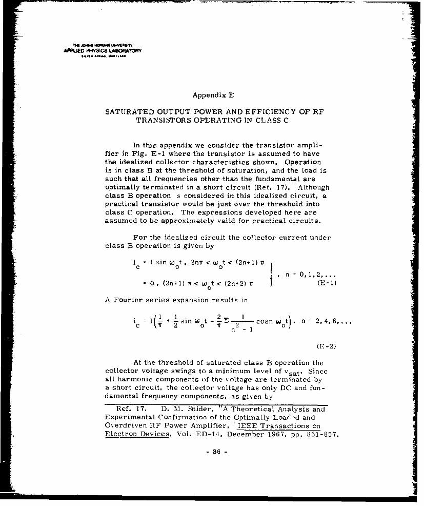
Appendix E
SATURATED OUTPUT POWER AND EFFICIENCY OF RFTRANSISTORS OPERATING IN CLASS C
In this appendix we consider the transistor ampli-fier in Fig. E-1 where the transistor is assumed to havethe idealized collector characteristics shown. Operationis in class B at the threshold of saturation, and the load issuch that all frequencies other than the fundamental areoptimally terminated in a short circuit (Ref. 17). Althoughclass B operation s considered in this idealized circuit, apractical transistor would be just over the threshold intoclass C operation. The expressions developed here areassumed to be approximately valid for practical circuits.
For the idealized circuit the collector current underclass B operation is given by
i - 1 sin w t , 2nrT < w t < (2n 1) T1C o 0
, n t 0,1,2,..
= 0, (2n+1) iT < w t < (2n+2) n - (E-1)O0
A Fourier series expansion results in
i:II 1. 2 1 WticI +1snW -cosn w~), n 2, 4. 6,..
2 0 IT n
(E-2)
At the threshold of saturated class B operation thecollector voltage swings to a minimum level of vsat* Sinceall harmonic components of the voltage are terminated bya short circuit, the collector voltage has only DC and fun-damental frequency components, as given by
Ref. 17. D.M. Snider, "A Theoretical Analysis andExperimental Confirmation of the Optimally Loarc'd andOverdriven RF Power Amplifier, " IEEE Transactions onElectron Devices. Vol. ED-14, December 1967, pp. 851-857.
-86 1
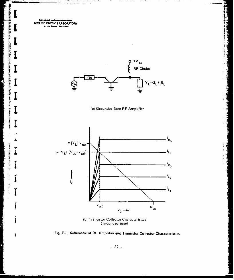
WOUD S USORATOY V1'i +Vc
Icc
I RF Choke
-- =Gy -
(a) Grounded Base RF Amplifier
Fi.E1Sceai o FApife n Tasso Colco Chrceitc
8= IYLI Vcc7 5
" i=lYLI (Vcc-Vsat)- =e4 i
, ie,
Vsat vvc Vcc
~(b) Transistor Collector Characteristics( grounded base)
Fig. E-1 Schematic of RF Amplifier and Transistor Collector Characteristics
-87
T'fE JON"S M~hi*jk UWIWMy
APPI4E1D M""I LMXMATOAYI
v V + -(V -V )sin (w t+9). (E-3)c cc cc sat 0
The relation between the fundamental componentsof collector current (1/2) and collector voltage is given by
1/2 (V -v )jyI (E-4)cc sat L
where
L L jBL at the fundameental frequency.
Transistor saturated output power is found from thecollector voltage across the real part cf -the load (DC blockEcd):
2P 1/2 (V -RF cc sat L (E-5)
The DC power supplied by the power supply is the productof supply voltage and D)C current:
P 1 IV (E-6)DC IT cc
Substituting from Eq. (E-4) yields
P 2 V E-7
The collector efficiency in a transistor amplifier is givenby
x (E /- 8 -)c RF DC
Substituting fromi Eqs. (E-5) and (E-6) results in
x 17 Vcc sat 1 IC; /YI(E-9X 4 L I.
Cc
-88-
APPUED "~tICS LABORATORY
o r
cc2
-89-

APPLIED PhYSCS LABORATORY
I NOMENC LATURE
A waveguide simulator width
Aef = effective antenna aperture area
a spacing between gratingsIb = dielectric thickness, die leci ric -filled guideheight
b =-height of coupled guide
B =waveguide simulator height
B = capacitive susceptance in aperture equivalentcircuit
B 2 =. inductive susceptance in aperture equivalentcircuit
B =inductive susceptance. partially filleddaa
B a = inductive susceptance, partially filled- T-junction
B at =inductive susceptance, dielectric -filledT -junction
B b = capacitive susceptance, partially filledbT T-junct ion
13- capacitive susceptance, dielectric -filledb( T-junction
-B csusceptance of symmetrical iris in air-filledguide
B susceptance of symmetrical iris in dielectric-filled guide
B 9capacitive susceptance. partially filledg L-jurction
BL transistor amplifier load susceptance
-91-
Preceding page blank

APPLMED PI4YiS LABORATORY
B () dielectric sheet susceptance
phase constant in dielectricd :circular probe diameter
d rectangular probe width
d # rectangular probe thickness
d E E-plane spacing
dH H-plane spacing
E electric field
-- free-space permittivity0
C relative dielectric constantr
7c =collector efficiency
6 = plane wave incident angle relative tolongitudinal direction
e = electrical length for balun cavity center to end
-- t plane wave incident angle relative tolongitudinal direction in dielectric
60 simulated scan angle
a electrical length of balun compensating lineS
phase between collector current and voltageG z transistor amplifier load conductance
Lg coupling slit width
h substrate thickness
I peak collector current
i c instantaneous collector current
i e =emitter current
n 120ff. intrinsic impedance of free space
X :free-space wavelength
c waveguide cut-off wavelength
92
"a JO""Oft"- A* *8- DAPPUEO PHYSCS LABORATORY
- = wavelength in dielectric
X waveguide wavelength in air-filled guide
Xg( = waveguide wavelength in dielectric -filledguide
SDC DC power
PRF = RF output power
R = grating resistors
RH = resistive part of Z 1
Re = resistive part of active element impedance
Rp z coaxial termination
- r = equivalent circuit resistance
R (s) = resistive part of active element impedance atprobe separation, s
AN R(w) = resistive part of active element impedance atprobe separation, w (strip edge)
4s -probe separation
t - time
T, T' reference planes
vc instantaneous collector voltage
1 Vcc - supply voltage
V 'sat = saturation voltage
I VSWR = voltage standing wave ratio
w z strip width
IX series reactance due to transformation length
,%a( grating inductive reactance in dielectric medium
X1 reactance of ZI
\ 2 reactance of short circuit stub w/2 in length
X 3 probe capacitive reactance
- 93 -
APJPLIFYSiC LAOCRATORY
X4 probe inductive reactance
Xa grating inductive reactance in free space
Xb grating capacitive reactance in free space
Xb(, grating capacitive reactance in dielectricmedium
YL transistor amplifier load admittance
YO= characteristic admittance. air-filled guideof height b'
YO( characteristic admittance, dielectric -fitledguide of height b
Yot characteristic admittance. guide of height b'zi aperture impedance looking out from strip edge
zc balun cavity characteristic impedance
Ze active element impedance at each probe
ZfS free space impedance per unit half-cell atscanned angle
zin balun input impedance
z 1. im-pedance of cacti balun output line
z 0 1 7characteristic impedance, air-filled guide
ZC character istic impedance in dielectric-filledregion
zs= impedance of balun compensating stub
frequency, rad/s
-94
I W11
APPLED PiYS= LASOMATOR-
REFERENCES
I1. J. L. Allen, "On Array Element Impedance Varia-
Vtion With Spacing." IEEE Transactions on Antennasand Propagation, Vol. AP-12. May 1964, pp. 371-"72. ..
2. E. V. Byron, "A New Flush Mounted Antenna Ele-ment for Phased Array Application," Proceedingsof the Phased-Arra, Antenna Symposium. 1970,pp. 187-192.
3. E. V. Byron, Antenna Aperture Design for ProjectCamel. API./JII" TG 1101, February 1970.
4. G. J. Laughlin. E. V. Byron. and T. C. Cheston."Very Wideband Phased-Array Antenna. " IEEETransactions on Antennas and Propagation. Vol.AP-20, November 19721. pp. 699-704.
5. P. W. Iannan and M. A. Balfour. "Simulation of aPhased-Array Antenna in Waveguide, " IEEE Trans-actions on Antennas and Propagation, Vol. AP-13.
I May 1965, pp. 342-353.
" £6. N. ,Marchand. 'Transmission-Line Conversion.Electronics, Vol. 17, December 1944. pp. 142-145.
7. \V. K. Roberts. "A New Wideband IRalun. Proceed-ings of the IRE. December 1957. pp. )628-1632.
8. J. W. Mcl.aughlin. 1). A. D1n, and R. W. Grow."A Wiciebancl Balun, " IRE Transactions on .Micro-wave Theory and Techniques, Vol. MlTT-6. July1958, pp. 314-316.
95-
APPLUED PHYSICS LABORATORY
9. R. Bawer and J. J. Wolfe. "A Printed CircuitBalun for Use With ,piral Antennas. " IRE Trans-actions on Microwave Theory and Techniques, Vol.MTT-8. May 1960, pp. 319-325.
10. G. OQtman. "The Compensated )3alun." IEEE Trans-actions of Microwave Theory and Techniques, Vol.NITT-14. 'March 1966, pp. 112-119.
11. Fl. R. Phelan. "A Wideband Parallel-ConnectedBalun," IEEE Transactions of Microwave Theoryand Techniques. Vol. MTT-18. May 1970. pp. 259-263.
12. G. .1. Laughlin, Patent 3,827.001, July 1974.
13. E. G. Magill and 1-. A. Wheeler. "Wide-Angle Im-i-pedance Matching of a Phased Array Anternna by aDielectric Sheet." IEEE Transactions on Antennasand Propagation, Vol. AP-14, .anuary 1966. pp. 49-53.
14. W. 1-. Leighton. R. .1. Chaffin. and J. G. Webb."RF Amplifier Design With Large Signal S-Parame-ters." IEEE Transactions on Microwave Theory andTechniques. Vol. M1TT-21. December 1973, pp. 809-814.
15. N. Marcuvitz. Wa\eguide 1tandbook. Vol. 10. N1itRadiation Laboratory Series. New York: McGraw-Hill. 1951.
16. C. C. Montgomery. R. II. Dicke. and F. I.. Pur-cell. Principles of Microwave Circuits. Vol. 8.MIT Radiation Laboratory Series. New York:McGraw-Hill. 1948. pp. 66-67.
17. D. M. Snider. 'A Theoretical :\nalysis and .xperi-mentaL Confirmation of the Optimally L.oaded and Over-drixen RF Power Amplifier. " IEEE Transactions onElectron Devices. Vol. El)-14. l)ecember 1967. pp.851-857.
- 96 -
INITIAL DISTRIBUTION EXTERNAL TO THE APPLIED PHYSICS LABORATORY*The work reported in TG 1278 was done under Navy Contract N00017-72-C-4401. This work is related to
Task A63A, which is supported by NAVSEASYSCOM (SEA-0341).
ORGANIZATION LOCATION ATTENTION No. o
DEPARTMENT OF DEFENSE I -------IICpe
DD C Alexandria, Va. 12
Department of the Nav
NAVSE.A Washington, D. C. SEA-0341 (S. A. Barham,T. Tasaka)2
SEA-652B (R. T. 11111) ISEA-09G3 2
NRL Washington, D. C. I.. Whicker I
NE LC San Diego, Cal. J. Hf. ProvencherI
NSE C Washington, D. C. R. D. L.endingI
NAVAIR Vbashinetrin, D. C. AIR-50174 2
NA VPRO Silver Spring, Mdl.1
C.ON 'R1A CTORS
M' ilncoln Iahoratory t.exinirtn 'Mass. (.BlakeI
Hfughes Aircraft Co. Fullerton, Cal. .1. AlIoka I
RCA Missile & Surface Radar Division Moorestown, N. .1. W. PattonI
Raytheon Santa itarbara. C~a]. 1). ArcherI
Sperry Cyroscopv Division G;rvat Nerk, N. Y. I.. Sch~a~tzmanI
Requests for copies of this report from DoD activities and contractors should be directed to DIDC,Cameron Station, Alexandria. Virginia 22314 using DDC Form I and, if necessary. DOC Form 55.
*Initial distribution of this document within the Applied Physics Laboratory has been maein accordance wntt a list on file in the APL Technical Publications Group,
-97-
Notices of availability of this report have been sent tothe following addressees, who comprise the distribution listfor Quarterly Report Research and Development Programs atThe Johns Hopkins University Applied Physics Laboratory,January-March 1975, APL/JHU C-RQR/75-1. They are notsent to offices listed in the initial distribution.
ORGANIZATION LOCATION ATTENTION
DEPARTMENT OI: I.*FNE
DDR&E Washingtn, D.C'. C'apt. It. (*. .\%rif
Dir. . WSEG Arlinotow,. V,.Tactical Technology Infn. Analysim (*tr. ('o1nl,1S, (0hin Nanv IIiIIDDC AIr-xanolris. Va.Information Ana!y.im ('tr., (CPIA ?4lver sprine. Mdl.Defense MappinR Ageny, Aprompae1
Ctr. M . l~nui.l. Mho. WKI;
Department of the Navy
Department Offies
CNO Wna.hinL-to,. I i. (. ( )I '-i;1
.1" \-f0:i
- 98-
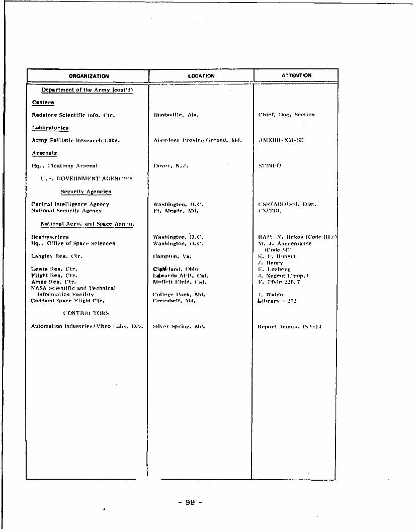
ORGANIZATION LOCATION ATTENTION
Department of the Army (cont'd)
Centers
Redstone Scientific Info. (tr. lieint5(ville, AIla. chief, DoCc. Section
Laboratories
Army Blal listic Rtesearch L ahP. Aiber-le-e,, 1'rviriLG~ rnund. N141. A Ni XlIM-NN.-SE-
Arsenlals
i~q., He1ictinny Arse'nal I)vvv. N...S!
U. S. ()VEINNIINT A;E-NCII1:S-'
Security Agencies
Central Intelligence Agency Wa-chingtmn. D.C. CS1( ADl)IMId. Dist.National Security Agency F~t. Meade. Md. r,3ITI*)l.
National Aerce. andl Space AdIniln.
Headquarters Washdingtoen. IM. . A!': N. liekos (Code I1l.0iiq.. office of Spar, Sciences Wambeitglon. 1).('. M. .1. Aticrernanne
(CoWe %,(;Langley lies. ctr. Ilamiplin. Va. K~. I.. Hutbert
.1. fienryLewis lies. Ctr. Clg.4-lanol. M~in F. l.C.het-LFlight lies. Ctr. F~wards All;. Cal. .1. Nugent (Prop.IAmes Iles. Ctr. RMrfett Field. (*al. F. i'fvie '228. 7NASA Scientific and! TIerhnical
lnrorma4',ion Facilltv CC'ileeL' Park. Uol. .1. WaldoGoddard Space Flight C*tr. (Creerhiwf. %I'I. Librarv - 2-12
CONTI ACTOIIS
Automation Industries/ Vitro t.ah . D~iv. Sii~o-r Spring. Pket. Hepor? Accplk. lDA-i-
-99-
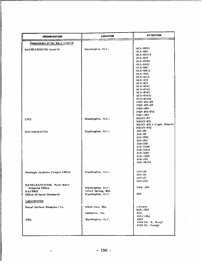
ORGANIZATION LCTO TETO
Department or the Navy (c'mt'd)
NAVSFASYSCON (ccoit'd) Wa41vptV.I..SI.A-032ASl-:A-0:33SlI:A-03:IIAStI.:A-034SKA-014I1SFA-046-Psi*:A-06(;S1:'A-09)(;3SE-A- 5.51SE'A -6512SEA-653SI-A-654SI-:A-6541SEA -694 2S*: A -6543SEA-65431SEA-65432PI'S 3104-20I'NlS 403-40IIMS-4 04l'NIS 404-032[PM'S-405
CN NI Washington, DX.(. NNIAI'-03NNIAl-031.NMAI',031.1 (capt. Krach)NNIAI-032
NAV'AIRSN'SCONl Waxhington. D).('. AIII-00AIR-03AIR -0311AIII-03CAliI-330A Il-S108AIJt-520AAlII -520C
AlR1-5203ATR-5935AIR-501 74
Strategic Systems Project offtice Was4hington. 1).C. SSII-20SS1 '-24SSI'-27SSP-272
NAVEL.EXSYS('OM. Nuvy Spac'eProjects Office Wa-4hington, D.(. PE106
NAVPRO silver Spring. Md.
Office of Naval Research Washington. D.('. 463
Laboratories
Naval Surface Weapons ('tr. White Oak. Md. LibraryN0I,-034
IDahlgren. Va. NIluI)R(:Colh~y
N RL Washlngtum. 1). c. 20276500o (%W. It, .sniy)1;0(6 (11. Gandy)
* -100-
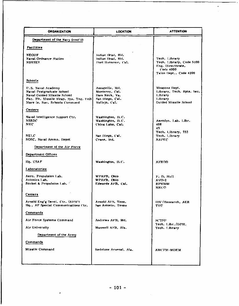
ORGANIZATION LOCATION ATTENTION
Department of the Navy (roiitd)
Facilities
NEODF Indiun I teai. Mdt.Naval Ordnance S-tation Indliun lhead, Md. Tech. LibraryNSWSES Port tlisenenw. Cal. Tech. Library. Code 5100
Eng. D~irectorate.C'ode 4000
'ralos Iept. . Code 4200
Schools
T. S. Naval Academy Annapolis. Md. Weapons D~ept.Naval Postgraduate School Monterey. Cat. Library. Tech. Rpts. Sec.Naval Guided Missile School D~am Neck. Va. LibraryPac. Fit. Mlissile Weap. Sys. Tng. Unit San D~iego, Cal. I.ibraryMare Is. Nat'. Schools Command Vallejo. Cal. Guided Missile School
Centers
Naval Intelligence Support Ctr. Washington. I). C.NSRDC Washington. 1). C. Aerodyn. lab. I.Ibr.NWC China t.ake. Cal. 406
415
Tech. 1,ibrary. 753NEL.C San D~iego, Cal. Tech. I.ibraryNOSC. Naval Ammo. Depot Crane. Ind. NAIFC
Department of the Air Force
Department Offices
lq. USAF Washington. D.C. AFRDD
Laboratories
Aero. Propulsion I.ab. WJ'AIFR. Ohio F. D). StullAvionics l.ab. WPAFI-. Ohio AVO-2Rocket & Propulsion Lab. Edwards A FR. Cal. RPMMM
Centers
Arnold Eng'g Devel. Ctr. (AiFSC) Arnold AlPS. Tenn. I)SC/ltesearch. AERHq. . AF Special Communications ('tr. San Antonio. Texas TI)T
Commands
Air Force Systems C:ommand Andre'ws AFB. Md. SCTSl1Tech. Ilibr. /DPSI.
Air University Maxwell Ai*'l. Ala. Tech. Ilibrary
Department of the Army
Commands
Missile Command Reudstone Arsenal. Ala. AMCI'M-mDFm
-101-


![%Ê'22 b4: G ^ ó/ b Ï X 8 Z - Nihon UniversityF 0 >& ¹ B25 º4 v1 ¥ D >' ^ ] b D í 5 G _ | ~ ' b P Â W W Z r 8 ~ r K S %Ê'22 b4: G ^ ó/ \'ö#. c>*%Ê'2* b s ^ } N%Ê'2 µ6õ](https://img.pdfslide.net/doc/110x75/5e6cbc48c5ed6112b5085546/22-b4-g-b-x-8-z-nihon-f-0-b25-4-v1-d-.jpg)


![y': ,/*l U) - York University · As .:*g r^"tw(l (t L"J tucrtf S?o s.\.'nztS L-rl a hAW t + 3+q) ( fZ) 'ivtftv'ct'r' n Jo ]oSth 6ra](https://img.pdfslide.net/doc/110x75/5fa048c395d0fb02106ed77b/y-l-u-york-as-g-rtwl-t-lj-tucrtf-so-snzts-l-rl-a.jpg)