Embed Size (px)
Citation preview

JOURNAL OF LIGHTWAVE TECHNOLOGY, VOL. 33, NO. 4, FEBRUARY 15, 2015 911
A Scalable, Low-Latency, High-Throughput, OpticalInterconnect Architecture Based on Arrayed
Waveguide Grating RoutersRoberto Proietti, Zheng Cao, Christopher J. Nitta, Yuliang Li, and S. J. Ben Yoo, Fellow, IEEE, Fellow, OSA
Abstract—This paper proposes, simulates, and experimen-tally demonstrates an optical interconnect architecture for large-scale computing systems. The proposed architecture, Hierarchi-cal Lightwave Optical Interconnect Network (H-LION), leverageswavelength routing in arrayed waveguide grating routers (AW-GRs), and computing nodes (or servers) with embedded routersand wavelength-specific optical I/Os. Within the racks and clus-ters, the interconnect topology is hierarchical all-to-all exploitingpassive AWGRs. For the intercluster communication, the proposedarchitecture exploits a flat and distributed Thin-CLOS topologybased on AWGR-based optical switches. H-LION can scale beyond100 000 nodes while guaranteeing up to 1.83× saving in numberof inter-rack cables, and up to 1.5× saving in number of inter-rack switches, when compared with a legacy three-tier Fat Treenetwork. Network simulation results show a system-wide networkthroughput reaching as high as 90% of the total possible capacityin case of synthetic traffic with uniform random distribution. Ex-periments show 97% intracluster throughput for uniform randomtraffic, and error-free intercluster communication at 10 Gb/s.
Index Terms—Arrayed waveguide grating routers (AWGRs),datacenter networking, optical interconnects, optical switches.
I. INTRODUCTION
THE landscape of today’s cyberinfrastructure is dominatedby innovations in data centers and high performance com-
puting (HPC) systems. As of January 2014, Google processesapproximately six billion searches per day [1] and Facebook datacenters serve 1.3 billion users who spend 640 billion minutesbrowsing monthly [2]. In scientific computing, analyses, simu-lations, and visualization of extreme data are enabled by HPCs.Both large scale data centers and HPC systems include manythousands of servers intimately networked with each other. AsAmdahl’s law [3] suggests, a parallel computing system withbalanced processing, memory, and communications can performoptimally across most applications. This indicates that an opti-mized petascale computing system requires ∼1 PB/s bisection
Manuscript received September 8, 2014; revised December 14, 2014 andJanuary 16, 2015; accepted January 16, 2015. Date of publication January 21,2015; date of current version February 20, 2015. This work was supported inpart under DoD Agreement Number: W911NF-13–1–0090.
R. Proietti, C. J. Nitta, and S. J. B. Yoo are with the Department of Electricaland Computer Engineering, University of California, Davis, CA 95616 USA (e-mail: [email protected]; [email protected]; [email protected]).
Z. Cao is with the Institute of Computing Technology, Chinese Academy ofSciences, Beijing 100190, China (e-mail: [email protected]).
Y. Li was with the Department of Electrical and Computer Engineering,University of California, Davis, CA 95616 USA. He is now with the Departmentof Computer Science, University of Southern California, Los Angeles, CA90089-0781 (e-mail: [email protected]).
Color versions of one or more of the figures in this paper are available onlineat http://ieeexplore.ieee.org.
Digital Object Identifier 10.1109/JLT.2015.2395352
bandwidth in addition to ∼1 PB memory and ∼1 petaFLOPSprocessors. Typical petascale data centers and computing sys-tems are already consuming on the order of many megawatts[4]. Scalability, efficiency, throughput, and latency of these largesystems are largely determined by those of the interconnectionnetworks [5]. Today’s interconnection networks typically relyon electronic-crossbar switches that store and forward packets[6], which may lead to limited scalability, capacity, throughput,and power-efficiency. Large-scale data centers and HPC systemsinevitably cascade such switches to interconnect a large num-ber of servers, adding complexity, inefficiency, and latency tothe systems. In order to support several hundreds of thousandsnodes, future data centers and HPCs must undergo completearchitectural and technological transformations so that they willmeet the necessary performance requirements while operatingwithin the power limits.
Optical interconnects can potentially bring transformativechanges to computing system architectures. Compared to elec-trical interconnects, optical interconnects provide (1) highertransmission bandwidth and lower energy consumption inde-pendently of distance, (2) inherent parallelism, (3) low inter-ference and crosstalk, and (4) low parasitic. In addition, op-tics offers wavelength (frequency) routing capability not avail-able in electronics with comparable size. As a result, opti-cally interconnected computing systems can potentially achieve(1) higher scalability and energy efficiency, (2) high-density par-allel links and buses overcoming input/output pin density limits,and (3) low-latency avoiding the need for including repeatersor switches with store-and-forward architectures. Further, op-tical devices with wavelength (frequency) routing capabilitycan achieve all-to-all interconnection between computing nodeswithout contention.
An arrayed waveguide grating router (AWGR) [7], [8] is anexample of devices with such wavelength routing capability.As Fig. 1(a) and (b) illustrate, the well-known wavelength rout-ing property of an AWGR allows any input port to communicatewith any output port simultaneously using different wavelengthswithout contention. Thus an N×N AWGR intrinsically providesall-to-all communication among N compute nodes in a flat topol-ogy using N wavelengths. Fig. 1(c) illustrates an N × N AWGRswitch with N compute nodes (Node 1-Node N Tx/Rx) witheach node having kt transmitters and kr receivers, respectively(1 ≤ kt, kr ≤ N ). Note that, only the TXs are tunable. Thisillustration assumes ring-resonator-based transmitters and mod-ulators with frequency selectivity. When kt = N and kr = N ,all-to-all interconnection without contention can be achieved in
0733-8724 © 2015 IEEE. Personal use is permitted, but republication/redistribution requires IEEE permission.See http://www.ieee.org/publications standards/publications/rights/index.html for more information.

912 JOURNAL OF LIGHTWAVE TECHNOLOGY, VOL. 33, NO. 4, FEBRUARY 15, 2015
Fig. 1. (a) N × N AWGR’s wavelength routing property (shown is N = 5example), (b) a wavelength assignment table. Here, m, m + 1 and m-1 representthree different grating orders (Free Spectral Ranges), and (c) LIONS with aN × N AWGR, N compute nodes, with each node having kt transmitters andkr receivers, respectively (1 + � kt , kr � N). This illustration assumes ringresonator based transmitters and modulators with frequency selectivity.
a flat topology. This case will be called passive AWGR switchor passive Low-latency Interconnect Optical Network Switch(LIONS) since no optical reconfiguration is necessary. If kr <N , contending conditions exist, and Ref. [9] demonstratedbuffered architecture and [10] presented bufferless all-opticaldistributed control plane with performance far greater than typ-ical electronic switches. If kt < N , then the transmitter must beable to tune its wavelength corresponding to the desired desti-nation node. This case will be called an active AWGR switch oractive LIONS. Ref. [9] investigated cases where kt = 1 (singletunable transmitter) and kr < N for a large scale rack-to-rackinterconnect network.
The active AWGR will have to deal with contention resolu-tion, even though the contention probability is minimized bythe use of kr RXs per output port and by the unique wavelengthrouting property in AWGR. Ref. [9], [10] show the performanceof different LIONS switch architectures interconnecting a num-
ber of nodes � 64 with kr = 4. Even with a limited amount ofRXs, the switch can sustain a throughput above 80% in caseof uniform random traffic. Round-robin arbitration and an all-optical first-come first-served arbitration schemes are used in[9], [10], respectively.
This paper investigates and demonstrates a scalable, low-latency, high-throughput, flat optical interconnect architectureemploying passive and active AWGR switches in a hierarchy.The proposed architecture, Hierarchical Lightwave Optical In-terconnect Network (H-LION), leverages wavelength routingin AWGRs, and computing nodes (or servers) with embeddedrouters and wavelength-specific optical I/Os.
Within the racks and clusters, the interconnect topology ishierarchical all-to-all exploiting passive AWGRs and embed-ded switches in the servers. For the inter cluster communica-tion, the proposed architecture exploits a flat and distributedthin-CLOS topology based on AWGR-based optical switches.As explained above, the active AWGR will have to handle someamount of contention, which will affect its performance in termsof throughput and latency. This could be overcome by using all-to-all passive interconnection also for inter-cluster communica-tion, at the expenses of a smaller scalability due to the limitednumber of TRXs available for inter-cluster interconnection.
The remainder of this paper is organized as follows.Section II reviews the related work. Section III introduces theproposed scalable interconnect architecture. Section IV presentsnetwork performance studies for the proposed architecture, andSection V demonstrates system emulation and experimentaltestbed studies by prototyping a cluster network involving AW-GRs and FPGA boards. Section VI concludes the paper.
II. RELATED WORK
Regarding network topologies based on electrical switches,Fat Tree (FT) [5], [11] is one of the most common architectureto build large-scale computing systems and it is usually builtwith some level of oversubscription to reduce the number ofinter-rack switches and cables. For a three-tier FT network with64-port electrical switches, the scalability of FT is well below100 000 nodes.
Flattened Butterfly (FB) [12], [13] is another possible inter-connect architecture. While FB can guarantee a smaller diametercompared to FT network (three hops instead of five), its scalabil-ity is also limited by the radix of the electrical switches, and themaximum number of interconnected nodes is also well below100 000 nodes, assuming to use 64-port electrical switches.
3-D Torus [14] is a well-known network topology for HPCsystems. Its scalability is not limited by the switch radix but thenetwork diameter grows quickly with the number of nodes.
The dragonfly topology [15] is a hierarchal network topologythat creates groups of nodes with an extremely high virtual radix.Ref. [15] does not provide details regarding the intra or the inter-group network, but it specifies that there is at least one global linkbetween any pair of groups. The authors also developed routingalgorithms that assure that the minimal path between any pair ofnodes uses at most one global link. While any arbitrary networkcan be used for the inter-group and intra-group networks, tominimize the worst-case hop count these networks should be

PROIETTI et al.: SCALABLE, LOW-LATENCY, HIGH-THROUGHPUT, OPTICAL INTERCONNECT ARCHITECTURE 913
all-to-all, i.e. all the routers in a group should be connected toeach other directly (otherwise, some local forwarding is requiredvia the intra-group network, which increases the hop count).
A recent trend in large-scale interconnection architectures isto use servers/computing nodes with embedded switches witha large number of ports to create directly connected networkssuch as PERCs from IBM [16]. Embedding the switch/routerdirectly in the node reduces the latency of the initial/final hop.Keeping the diameter of the network small helps to reduce thenetwork’s average latency which is strongly correlated with theaverage number of hops between each source and destinationpairs. Researchers at HP have even proposed [17], [18] integrat-ing photonics into high radix switches in order to meet the needsof future high performance systems.
Concerning the use of optical technologies to improve per-formance or scalability of electrical interconnect architectures,Helios [20] is a popular hybrid electrical/optical switch architec-ture for modular datacenters that uses slow optical switches foroptical circuit switching and a legacy FT topology for electricalpacket switching. In addition, Helios’ design does not addressthe challenges of scalability. The main focus is to offload thehigh-bandwidth traffic to the optical network.
Calabretta et al. proposes and experimentally demonstrates aflat and distributed optical packet switching interconnect archi-tecture for inter-cluster communication [20]. The intra clusternetwork still makes use of legacy electrical networks.
The AWGR based optical switches and optical routers withpacket switching capability have been investigated for a num-ber of years [21]–[23], [11], [24]–[28]. Previous works [11],[21], [24]–[28] mainly focused on applying AWGR techniquesin access and telecommunication networks. However, the wave-length parallelism on AWGR outputs to achieve output queuingwas not explored in those designs due to the need to ensurewavelength consistency on the input and output fibers. Ref. [9]introduced LIONS (initially named as DOS) and the use ofAWGR to achieve output queuing in the optical domain. Ref.[10] presented a significant improvement over the architectureoriginally proposed in [9] by introducing the all-optical dis-tributed control plane based on the optical-TOKEN techniqueand the all-optical NACK. The simulation comparison in [29]shows that LIONS provides low-latency and high-throughputswitching without saturation even at very high (∼90%) inputload. Ref. [30] introduces an optical switch architecture basedon a combination of wavelength routing in AWGR and delivery-coupling-switch fabricated on a single planar lightwave circuit.The architecture can potentially scale beyond 512-ports, but nonetwork performance studies have been reported.
Research efforts in silicon photonics and photonic integratedcircuits can bring advantages in terms of power consumptionand bandwidth. For instance, researchers at HP [31] proposedphotonic I/Os to increase the per-port switch bandwidth up to320 Gb/s by using 32 wavelengths per fiber and having eachwavelength operating at 10 Gb/s. Ref. [32] shows a commer-cial development of a router chip with 168 optical I/Os andan aggregate bandwidth of 1.34 Tb/s. Ref. [33]–[35] reportadvancements and demonstrations of silicon photonics (SiP)WDM solutions. Silicon photonic LIONS in the configurationshown in Fig. 1(c) with 32 transmitters and 32 receivers utilizing
8 × 8 AWGR with kt = kr = 4 have been recently demon-strated [35] on a compact 1.2 mm× 2.4 mm silicon-on-insulatorplatform.
Traffic statistics and patterns in data centers are rarely dis-cussed in most publications, but some recent papers show thata strong communication locality within racks exists [36] andthat some applications (e.g. map reduce) running in data centersexhibit all-to-all communication patterns [37]. In this paper wediscuss a scalable and flat interconnection topology supportingboth locality and all-to-all communications.
III. H-LION: INTERCONNECT ARCHITECTURE EXPLOITING
AWGRS IN HIERARCHY
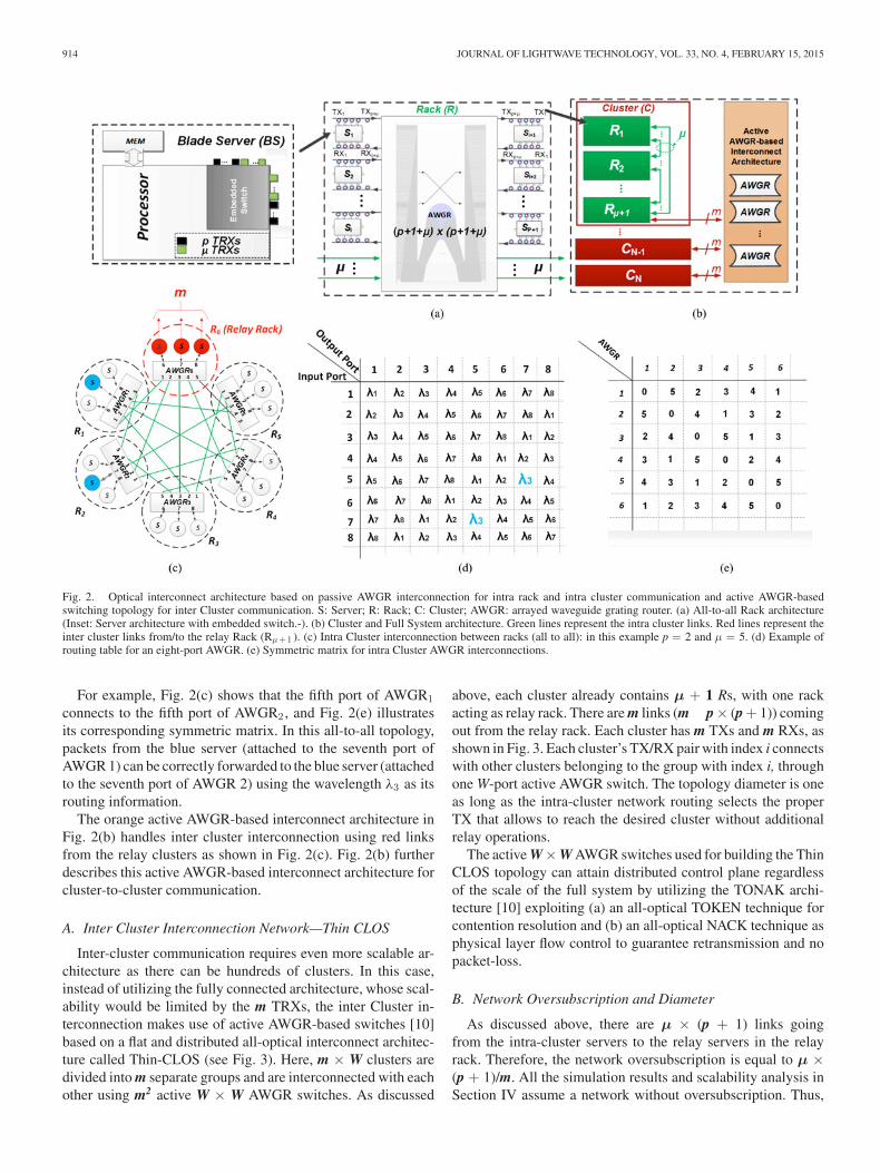
Fig. 2(a), (b), and (c) illustrate the proposed hierarchical op-tical interconnect architecture (H-LIONS), which is organizedin Servers (S), Racks (R) and Clusters (C). The proposed inter-connect architecture exploits passive AWGR (passive-LIONS)all-to-all interconnection for intra rack and intra cluster com-munication, while inter cluster communication is provided bya flat active AWGR switch topology with distributed control(Thin-CLOS, Ref. [10]).
The computing node, i.e. Server (S), has one embedded elec-trical switch with WDM optical I/Os. The embedded switchperforms the routing function within the server to forward thepackets to the proper TRX port based on the destination addressof the packets. The p TRXs are used to connect with other Ssin the same R through all-to-all interconnection of the passiveAWGR within the same R. The μ TRXs are used to connect withSs in different Rs within the same Cluster. This interconnectionalso makes use of wavelength-specific TRXs and each S can actas a relay (the maximum number of hops in one C is two).
Different Rs in a C are directly connected with each othersupporting all-to-all interconnection using multiple passive AW-GRs shown in Fig. 2(c). There are p + 1 S’s in each R, and μ+ 1 R’s in each C. Note that, one of the racks in the cluster,i.e. R6 in Fig. 2(c), acts as a relay rack for the traffic goingin and out from the cluster. In total, the relay Rack has μ ×(p + 1) TRXs for distributing the incoming traffic to the in-tra cluster nodes, and there can be up to p × (p + 1) TRXsfor inter cluster communication. We define m to be the num-ber of TRXs for communication with other clusters (m � p ×(p + 1)). Fig. 2(a) illustrates the architecture of R with all-to-allconnectivity among p + 1 Ss. The inset of Fig. 2(a) shows thearchitecture of the server (S) with the embedded switch and p +μ wavelength-specific transceivers (TRXs).
To perform correct intra-cluster routing, we use an all-to-alltopology built following a symmetric matrix shown in Fig. 2(e).If we label AWGRs as AWGR0 , AWGR1 , . . . , AWGRn anddefine the element aij in the matrix as the sequence number ofthe port to connect AWGRi with AWGRj , then we define thesymmetric matrix as:
⎧⎪⎪⎨
⎪⎪⎩
aij = aji 1 ≤ i ≤ n 1 ≤ j ≤ n i �= j;aij = 0 i = ja1j ∩ a2j ∩ . . . ∩ anj = ∅ 1 ≤ j ≤ nai1 ∩ ai2 ∩ . . . ∩ ain = ∅ 1 ≤ i ≤ n.
(1)
914 JOURNAL OF LIGHTWAVE TECHNOLOGY, VOL. 33, NO. 4, FEBRUARY 15, 2015
Fig. 2. Optical interconnect architecture based on passive AWGR interconnection for intra rack and intra cluster communication and active AWGR-basedswitching topology for inter Cluster communication. S: Server; R: Rack; C: Cluster; AWGR: arrayed waveguide grating router. (a) All-to-all Rack architecture(Inset: Server architecture with embedded switch.-). (b) Cluster and Full System architecture. Green lines represent the intra cluster links. Red lines represent theinter cluster links from/to the relay Rack (Rμ+1 ). (c) Intra Cluster interconnection between racks (all to all): in this example p = 2 and μ = 5. (d) Example ofrouting table for an eight-port AWGR. (e) Symmetric matrix for intra Cluster AWGR interconnections.
For example, Fig. 2(c) shows that the fifth port of AWGR1connects to the fifth port of AWGR2 , and Fig. 2(e) illustratesits corresponding symmetric matrix. In this all-to-all topology,packets from the blue server (attached to the seventh port ofAWGR 1) can be correctly forwarded to the blue server (attachedto the seventh port of AWGR 2) using the wavelength λ3 as itsrouting information.
The orange active AWGR-based interconnect architecture inFig. 2(b) handles inter cluster interconnection using red linksfrom the relay clusters as shown in Fig. 2(c). Fig. 2(b) furtherdescribes this active AWGR-based interconnect architecture forcluster-to-cluster communication.
A. Inter Cluster Interconnection Network—Thin CLOS
Inter-cluster communication requires even more scalable ar-chitecture as there can be hundreds of clusters. In this case,instead of utilizing the fully connected architecture, whose scal-ability would be limited by the m TRXs, the inter Cluster in-terconnection makes use of active AWGR-based switches [10]based on a flat and distributed all-optical interconnect architec-ture called Thin-CLOS (see Fig. 3). Here, m × W clusters aredivided into m separate groups and are interconnected with eachother using m2 active W × W AWGR switches. As discussed
above, each cluster already contains μ + 1 Rs, with one rackacting as relay rack. There are m links (m � p× (p + 1)) comingout from the relay rack. Each cluster has m TXs and m RXs, asshown in Fig. 3. Each cluster’s TX/RX pair with index i connectswith other clusters belonging to the group with index i, throughone W-port active AWGR switch. The topology diameter is oneas long as the intra-cluster network routing selects the properTX that allows to reach the desired cluster without additionalrelay operations.
The active W×W AWGR switches used for building the ThinCLOS topology can attain distributed control plane regardlessof the scale of the full system by utilizing the TONAK archi-tecture [10] exploiting (a) an all-optical TOKEN technique forcontention resolution and (b) an all-optical NACK technique asphysical layer flow control to guarantee retransmission and nopacket-loss.
B. Network Oversubscription and Diameter
As discussed above, there are μ × (p + 1) links goingfrom the intra-cluster servers to the relay servers in the relayrack. Therefore, the network oversubscription is equal to μ ×(p + 1)/m. All the simulation results and scalability analysis inSection IV assume a network without oversubscription. Thus,

PROIETTI et al.: SCALABLE, LOW-LATENCY, HIGH-THROUGHPUT, OPTICAL INTERCONNECT ARCHITECTURE 915
Fig. 3. Thin CLOS topology interconnecting m × W clusters: m groups, with each group containing W clusters. W is the port-count of active AWGR switches.
TABLE IDESIGN PARAMETERS TO ACHIEVE A NETWORKS SCALE � 100 000 SERVERS
WITHOUT OVERSUBSCRIPTION
W p μ m N
32 20 3 63 127 00816 19 4 80 102 40012 18 5 95 108 30010 17 6 108 116 6408 16 7 119 113 2887 15 8 128 114 688
m = μ × (p + 1). For a fair comparison, the scalability analysisand simulation results for the FT network also assume a networkwithout oversubscription.
The network diameter for the proposed architecture is equal to5 (two hops for intra cluster, one hop for inter cluster, two hopsfor intra cluster). The FT network has also a network diameterequal to five in the case of a three-tier FT.
C. Scalability Analysis
The radix of the AWGR is an important consideration in de-termining the scalability of the interconnect networks. Whilehigh port count silicon-photonic AWGRs with 512-ports havebeen experimentally demonstrated [38], in-band crosstalk andthe number of wavelengths become challenging. Noting that32-port AWGRs are commercially available and that 64-portAWGRs were demonstrated in as early as 2003 [7] with<−40 dB crosstalk and ∼6 dB insertion loss, we believe thatthe use of AWGRs with a port count value up to 64 is a vi-able solution both for passive AWGR interconnection and ac-tive AWGR switches (the scalability of active AWGR switchesmainly depends on the crosstalk level of the passive AWGR init). Therefore, we will limit our discussions to AWGRs with portcounts not higher than 64.
In the proposed architecture, the number of servers is N =[(p + 1) × μ] × m × W (we do not count the servers in therelay rack as computing nodes), the number of passive AWGRis NAWGR p = (μ + 1) × m × W , and the number of ac-tive AWGR switches is NAWGR a = m2 . Table I shows somepossible combinations of p, μ and m parameters to achieve anetwork scale beyond 100 000 servers. The assumptions hereare: (a) oversubscription = 1, which means m = (p + 1) × μ,and (b) number of wavelengths � 32. The limit on the num-
Fig. 4. Number of inter-rack cables as function of the number of servers forH-LION and FT architectures without oversubscription.
Fig. 5. Number of inter-rack switches as function of the number of serversfor H-LION and FT architectures without oversubscription.
ber of wavelengths translates into the following conditions: 1)W ≤ 32 for the Thin CLOS architecture; 2) p + μ ≤ 32.
Figs. 4 and 5 show the number of inter-rack bidirectional linksand switches, respectively. We perform the comparison with astandard m-port n-tree FT networks without oversubscription,where m is the port count of the single electrical switch and thenumber of layers in the FT network is n = 3. The number ofservers, cables and switches in Figs. 4 and 5 are calculated forthe following values of m = 38, 48, 64, 72, 80. The total numberof servers is NFT = 2 × (m/2)n ; the total number of switchesis NS = (2n − 1) × (m/2)n−1 , while the total number of inter-rack switches is NS – NFT /(m/2). Finally, the number of cablesis equal to NC = (NS × m − NFT).
916 JOURNAL OF LIGHTWAVE TECHNOLOGY, VOL. 33, NO. 4, FEBRUARY 15, 2015
TABLE IISIMULATION PARAMETERS
Parameter Value Parameter Value
VC’s Buffer size 4 Kbyte SerDes RX TX Delay (GTH) 113 ns � 14 (Cycles)Delay in Receiver Module (RX) 4 (Cycles) Wire Delay per meter 5 nsDelay in Transmit Module (TX) 4 (Cycles) Delay in Passive AWGR 1 nsSwitching Delay (Crossbar) 5 (Cycles) Active AWGR Switching 12 ns
In the proposed architecture, the number of active switchesis NAWGR a = m2 = (p + 1)2 × μ2 , while the number ofcables is NC = 2 × W × [(p + 1) × μ]2 + [(p + 1) × μ ×W ] × [μ × (μ + 1)]. The first term represents the number ofactive switches multiplied for the AWGR port count (the factor“2” account for both input and output ports).
The curves in Figs. 4 and 5 are calculated assuming a constantμ = 3.
For the parameters indicated in Figs. 4 and 5, the proposedarchitecture at a scale of >60 000 nodes guarantees up to 1.84× savings in terms of inter-rack cables, and up to 1.5 × savingsin terms of inter-rack switches. Note that, based on the formulaabove, the lower the μ, the higher the savings in terms of numberof cables.
IV. PERFORMANCE STUDIES
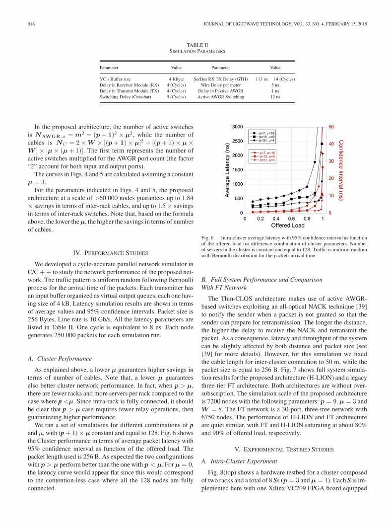
We developed a cycle-accurate parallel network simulator inC/C + + to study the network performance of the proposed net-work. The traffic pattern is uniform random following Bernoulliprocess for the arrival time of the packets. Each transmitter hasan input buffer organized as virtual output queues, each one hav-ing size of 4 kB. Latency simulation results are shown in termsof average values and 95% confidence intervals. Packet size is256 Bytes. Line rate is 10 Gb/s. All the latency parameters arelisted in Table II. One cycle is equivalent to 8 ns. Each nodegenerates 250 000 packets for each simulation run.
A. Cluster Performance
As explained above, a lower μ guarantees higher savings interms of number of cables. Note that, a lower μ guaranteesalso better cluster network performance. In fact, when p > μ,there are fewer racks and more servers per rack compared to thecase where p <μ. Since intra-rack is fully connected, it shouldbe clear that p > μ case requires fewer relay operations, thenguaranteeing higher performance.
We ran a set of simulations for different combinations of pand μ, with (p + 1) × μ constant and equal to 128. Fig. 6 showsthe Cluster performance in terms of average packet latency with95% confidence interval as function of the offered load. Thepacket length used is 256 B. As expected the two configurationswith p > μ perform better than the one with p < μ. For μ = 0,the latency curve would appear flat since this would correspondto the contention-less case where all the 128 nodes are fullyconnected.
Fig. 6. Intra-cluster average latency with 95% confidence interval as functionof the offered load for difference combination of cluster parameters. Numberof servers in the cluster is constant and equal to 128. Traffic is uniform randomwith Bernoulli distribution for the packets arrival time.
B. Full System Performance and ComparisonWith FT Network
The Thin-CLOS architecture makes use of active AWGR-based switches exploiting an all-optical NACK technique [39]to notify the sender when a packet is not granted so that thesender can prepare for retransmission. The longer the distance,the higher the delay to receive the NACK and retransmit thepacket. As a consequence, latency and throughput of the systemcan be slightly affected by both distance and packet size (see[39] for more details). However, for this simulation we fixedthe cable length for inter-cluster connection to 50 m, while thepacket size is equal to 256 B. Fig. 7 shows full system simula-tion results for the proposed architecture (H-LION) and a legacythree-tier FT architecture. Both architectures are without over-subscription. The simulation scale of the proposed architectureis 7200 nodes with the following parameters: p = 9,μ = 3 andW = 8. The FT network is a 30-port, three-tree network with6750 nodes. The performance of H-LION and FT architectureare quiet similar, with FT and H-LION saturating at about 80%and 90% of offered load, respectively.
V. EXPERIMENTAL TESTBED STUDIES
A. Intra-Cluster Experiment
Fig. 8(top) shows a hardware testbed for a cluster composedof two racks and a total of 8 Ss (p = 3 and μ = 1). Each S is im-plemented here with one Xilinx VC709 FPGA board equipped

PROIETTI et al.: SCALABLE, LOW-LATENCY, HIGH-THROUGHPUT, OPTICAL INTERCONNECT ARCHITECTURE 917
Fig. 7. Full-system H-LION network performance 7200 servers (p = 9, μ =3, m = 30, W = 8). Performance of a 6750-server three-tree FT network with-out oversubscription is shown for comparison. Traffic has uniform random dis-tribution with Bernoulli process for the packets arrival time. Average packetlatency with 95% confidence interval as function of the offered load.
Fig. 8. (Top) Picture of the hardware demo using eight VIRTEX 7 FPGAbaords and two 32-port AWGRs. (Bottom) Latency vs. Throughput performancecomparison between hardware and simulations.
with a Virtex 7 chip. Each FPGA implements the traffic gen-eration function and the embedded switch (see Fig. 9 for moredetails) and has four 10 Gb/s WDM SFP + transceivers (TRXs):three for all-to-all intra rack communication and one for interrack communication (within the same cluster). The wavelengthsused for the experiment are in the range 1546.04–1561.04 nm,with a 0.4 nm (50 GHz) frequency grid. The network trafficgenerated by the FPGAs is converted in the optical domain,wavelength-routed by two 32-port AWGRs (one per rack) and
Fig. 9. Architecture of the embedded switch inside the VIRTEX 7 FPGA.
received by the destination servers (FPGAs). The insertion lossof the AWGRs is 8 dB. The TRXs have an output power of∼3 dBm and a sensitivity of −26 dBm at BER = 10−12, asshown in the black BER curve reported in Fig. 11.
Fig. 8(bottom) shows that, under uniform random traffic,the normalized system-wide network throughput of our clus-ter testbed is higher than 97% with the latency below 364 ns,only limited by the FPGA speed. In addition, using the param-eters measured from the testbed (see Table II), a very similarperformance curve can be obtained from the cycle-accurate sim-ulator. This is an important fact that validates the accuracy ofthe simulator. The packet size used for the simulation and ex-periment is 256 B. The slight difference between the simulationand experiment results is likely due to the differences in thecharacteristics of the random traffic generation in the servers.Flow-control mechanism implemented in the testbed and simu-lator avoids any packet loss.
Fig. 9 shows the architecture of the emulated embeddedswitch and traffic generator inside the FPGA VIRTEX 7 chip.The core switching fabric is an 11 × 5 crossbar [including thevirtual channels (VCs)]. We use a matrix arbiter which can im-plement one-cycle fair arbitration to perform the arbitration inthe 11× 5 crossbar. The Inter Rack port (the green port in Fig. 9)has four VCs: one for the packets directed to the server, and threeVCs for redirecting in the incoming packets to the other threenodes in the same rack. The traffic generator has also four VCs,one for each of the Intra Rack ports and Inter Rack port. In anall-to-all fashion, the Intra Rack ports (red ports) do not needVCs since these ports only communicate with the injection port(traffic checker).
In the demo of Fig. 8, p = 3 and μ = 1, while the AWGRradix is 32. In the case where the two racks would be fullypopulated (p + 1 + μ = 32), it is reasonable to expect somepower penalty due to accumulated inband crosstalk at each

918 JOURNAL OF LIGHTWAVE TECHNOLOGY, VOL. 33, NO. 4, FEBRUARY 15, 2015
Fig. 10. (Top) Inter-cluster communication experiment setup. TL-TX: tunable transmitter; TOA: tunable optical attenuator; AWGR: arrayed waveguide gratingrouter. (Bottom) Received waveforms for inter-cluster communication from C1 and C2 to C3.
of the AWGR output ports. However, for the 32-port com-mercial device used in this experiment, the crosstalk level isbelow −35 dB, which can still guarantee error-free operation[40], [41].
B. Inter-Cluster Experiment
This sub-section shows an experimental demonstration ofinter-cluster communications. Fig. 10(top) shows the three-Cluster experiment setup. C1 is the cluster described abovewith eight FPGA boards. FPGA1 (server #1) acts now also asthe relay server for inter-cluster communication. C2 and C3are emulated with two additional FPGA boards. Each clusterhas one 10 Gb/s NRZ-OOK TX with a fast tunable laser (TL)and a 10 Gb/s SFP + RX. Each cluster can communicate withthe other ones through wavelength routing in AWGR3 (eightports, 200 GHz spacing, 8 dB insertion loss). We emulated theoptical TONAK system (to solve the network contention) withan FPGA that implements a first-come first-served arbitrationscheme. The transmitted packets have random length (64 ∼2048 B) and contain different portions of 231 – 1 PRBS.
Fig. 11 shows the measured bit-error-rate (BER) data. First,we show a contention-less scenario where server #4 in C1 sendspackets to server #9 in C2 (red curve) and server #9 in C2 sendspackets to server #17 in C3 (blue curve). The BER was mea-sured with a BER tester implemented in the FPGAs. C2-C3BER curve shows 1-dB penalty due to non-optimum extinctionratio at the tunable TX output. Second, we show a scenario withnetwork contention where C1 and C2 send packets to C3 withrandom arrival time. To avoid resynchronization in the FPGAGTH receiver, tunable optical delay lines in each transmissionpath guarantee clock-phase matching of the packets at AWGRoutput 3. Note that, as for any optical packet switch system, anactual implementation would require to use burst-mode clockrecovery technology (as demonstrated in [42]–[44]) to recover
Fig. 11. BER measurements for intra cluster communications and hierarchicalinter cluster communications. Black dots: BER for packets going from S4 toS1; Red squares: BER for packets going from S1 to S9. Blue triangles: BER forpackets going from S9 to S17. Green triangles: BER for packet switching fromC1 and C2 to C3.
the clock on a packet-by-packet basis. Fig. 10(bottom) showsa snapshot of the received packets captured with Xilinx Chip-Scope analyzer tool. Fig. 11 shows measured BER curves forintra cluster communications (black curve) and hierarchical in-ter cluster communications where the green curve is a plot forinter-cluster C1 and C2 switching to C3, the red curve is forC1 switching to C2, and the blue curve is for C2 switching toC3. Note that, when errors occur at the switching point, the bytemisalignment in the GTH RX damages the full packet. As a con-sequence the BER increases significantly when the RX power isbelow −26.5 dBm. In all cases error-free (BER < 10−12) resultshave been obtained for RX power >−24 dBm.
PROIETTI et al.: SCALABLE, LOW-LATENCY, HIGH-THROUGHPUT, OPTICAL INTERCONNECT ARCHITECTURE 919
VI. CONCLUSION
We proposed a scalable optical interconnect architecturebased on a topology enabled by wavelength routing in AWGRsand by servers with embedded switches and optical I/Os. Theproposed architecture exploits AWGR-based all-to-all passiveinterconnection for intra-rack and intra-cluster communicationand AWGR-based active switching for inter-cluster communi-cation, supporting scalability beyond 100 000 nodes. Networksimulation results show throughput as high as 90% in case oftraffic with uniform random distribution. A testbed demonstra-tion shows system-wide network throughput at 97% for eightcompute nodes and two clusters, with measured Latency-vs.-Throughput data plots closely matching the data plots from thecycle-accurate simulator developed for the AWGR-based inter-connect network.
As discussed above, the AWGR radix is limited by thecrosstalk, which is also affected by the AWGR channel spacingand the number of wavelengths used in the system. However,Thin-CLOS topology can provide the same all-to-all topologyand logical performance as one large N × N AWGR with Nwavelengths but using m groups of W × W AWGRs with Wwavelengths only (W = N/m). The fewer number of wave-lengths allows to solve the crosstalk issue while requiring morefibers.
Areas of studies to further improve the network performanceinclude control plane and routing algorithms in combinationwith flexible bandwidth technologies to dynamically adjust thebandwidth of the different links according to the real traffic de-mand. This can help reducing the congestion between hotspotswhile saving energy for the links with low utilization.
REFERENCES
[1] StatisticBrain. (2014). Google Annual Search Statistics [Online]. Avail-able: http://www.statisticbrain.com/google-searches/
[2] StatisticBrain. (2014). Facebook Statistics. [Online]. Available: http://www.statisticbrain.com/facebook-statistics/
[3] G. Amdahl, “Validity of the single processor approach to achieving large-scale computing capabilities,” in Proc. Spring Joint Comput. Conf., 1967,pp. 483–485.
[4] P. M. Kogge and T. J. Dysart, “Using the TOP500 to trace and projecttechnology and architecture trends,” presented at the International Conf.High Performance Computing, Networking, Storage and Analysis, Seattle,WA, USA, 2011.
[5] M. Al-Fares, A. Loukissas, and A. Vahdat, “A scalable, commodity datacenter network architecture,” SIGCOMM Comput. Commun. Rev., vol. 38,pp. 63–74, 2008.
[6] F. Abel, C. Minkenberg, I. Iliadis, T. Engbersen, M. Gusat, F. Gramsamer,and R. P. Luijten, “Design issues in next-generation merchant switchfabrics,” IEEE-ACM Trans. Netw., vol. 15, no. 6, pp. 1603–1615, Dec.2007.
[7] S. Kamei, M. Ishii, M. Itoh, T. Shibata, Y. Inoue, and T. Kitagawa, “64 x64-channel uniform-loss and cyclic-frequency arrayed-waveguide gratingrouter module,” Electron. Lett., vol. 39, pp. 83–84, 2003.
[8] B. Glance, I. P. Kaminow, and R. W. Wilson, “Applications of the inte-grated waveguide grating router,” J. Lightw. Technol., vol. 12, no. 6, pp.957–962, Jun. 1994.
[9] X. Ye, P. Mejia, Y. Yin, R. Proietti, S. J. B. Yoo, and V. Akella, “DOS—Ascalable optical switch for datacenters,” in Proc. ACM/IEEE Symp. Archit.Netw. Commun. Syst., 2010, pp. 1–12.
[10] R. Proietti, Y. Yin, R. Yu, C. J. Nitta, V. Akella, C. Mineo, and S. J. B. Yoo,“Scalable optical interconnect architecture using AWGR-based TONAKLION switch with limited number of wavelengths,” J. Lightw. Technol.,vol. 31, no. 24, pp. 4087–4097, Dec. 15, 2013.
[11] M. C. Chia, D. K. Hunter, I. Andonovic, P. Ball, I. Wright, S. P. Ferguson,K. M. Guild, and M. J. O’Mahony, “Packet loss and delay performanceof feedback and feed-forward arrayed-waveguide gratings-based opticalpacket switches with WDM inputs-outputs,” J. Lightw. Technol., vol. 19,no. 9, pp. 1241–1254, Sep. 2001.
[12] W. J. Dally and B. P. Towles, Principles and Practices of InterconnectionNetworks. Amsterdam, The Netherlands: Elsevier, 2004.
[13] J. Kim, W. J. Dally, and D. Abts, “Flattened butterfly: A cost-efficienttopology for high-radix networks,” ACM SIGARCH Comput. Archit. News,vol. 35, pp. 126–137, 2007.
[14] S. Horiguchi and T. Ooki, “Hierarchical 3D-torus interconnection net-work,” in Proc. Int. Symp. Parallel Archit., Algorithms Netw., 2000, pp.50–56.
[15] J. Kim, W. J. Dally, S. Scott, and D. Abts, “Technology-driven, highly-scalable dragonfly topology,” ACM SIGARCH Comput. Archit. News, vol.36, pp. 77–88, 2008.
[16] B. Arimilli, R. Arimilli, V. Chung, S. Clark, W. Denzel, B. Drerup, T.Hoefler, J. Joyner, J. Lewis, L. Jian, N. Nan, and R. Rajamony, “ThePERCS high-performance interconnect,” in Proc. IEEE 18th Annu. Symp.High Perform. Interconnects, 2010, pp. 75–82.
[17] N. Binkert, A. Davis, N. P. Jouppi, M. McLaren, N. Muralimanohar, R.Schreiber, and J. H. Ahn, “The role of optics in future high radix switchdesign,” in Proc. 38th Annu. Int. Symp. Comput. Archit., 2011, pp. 437–447.
[18] R. G. Beausoleil, “Large-scale integrated photonics for high-performanceinterconnects,” ACM J. Emerging Technol. Comput. Syst., vol. 7, p. 6,2011.
[19] N. Farrington, G. Porter, S. Radhakrishnan, H. H. Bazzaz, V. Subramanya,Y. Fainman, G. Papen, and A. Vahdat, “Helios: A hybrid electrical/opticalswitch architecture for modular data centers,” SIGCOMM Comput. Com-mun. Rev., vol. 40, pp. 339–350, 2010.
[20] W. Miao, J. Luo, S. Di Lucente, H. Dorren, and N. Calabretta, “Novelflat datacenter network architecture based on scalable and flow-controlledoptical switch system,” Opt. Express, vol. 22, pp. 2465–2472, Feb. 2014.
[21] S. J. B. Yoo, “Optical packet and burst switching technologies for thefuture photonic Internet,” J. Lightw. Technol., vol. 24, no. 12, pp. 4468–4492, Dec. 2006.
[22] M. J. O’Mahony, D. Simeonidou, D. K. Hunter, and A. Tzanakaki, “Theapplication of optical packet switching in future communication net-works,” IEEE Commun. Mag., vol. 39, no. 3, pp. 128–135, Mar. 2001.
[23] C. Guillemot, M. Renaud, P. Gambini, C. Janz, I. Andonovic, R.Bauknecht, B. Bostica, M. Burzio, F. Callegati, M. Casoni, D. Chiaroni,F. Clerot, S. L. Danielsen, F. i. Dorgeuille, A. Dupas, A. Franzen, P. B.Hansen, D. K. Hunter, A. Kloch, R. Krahenbuhl, B. Lavigne, A. L. Corre,C. Raffaelli, M. Schilling, J.-C. Simon, and L. Zucchelli, “Transparent op-tical packet switching: The European ACTS KEOPS project approach,” J.Lightw. Technol., vol. 16, no. 12, pp. 2117–2134, Dec. 1998.
[24] H. Yang and S. J. B. Yoo, “Combined input and output all-optical variablebuffered switch architecture for future optical routers,” IEEE Photon.Technol. Lett., vol. 17, no. 6, pp. 1292–1294, Jun. 2005.
[25] M. Maier, M. Scheutzow, and M. Reisslein, “The arrayed-waveguidegrating-based single-hop WDM network: An architecture for efficientmulticasting,” IEEE J. Select. Areas Commun., vol. 21, no. 9, pp. 1414–1432, Nov. 2003.
[26] S. Bregni, A. Pattavina, and G. Vegetti, “Architectures and performanceof AWG-based optical switching nodes for IP networks,” IEEE J. Select.Areas Commun., vol. 21, no. 7, pp. 1113–1121, Sep. 2003.
[27] W. D. Zhong and R. S. Tucker, “Wavelength routing-based photonic packetbuffers and their applications in photonic packet switching systems,” J.Lightw. Technol., vol. 16, no. 10, pp. 1737–1745, Oct. 1998.
[28] D. Banerjee, J. Frank, and B. Mukherjee, “Passive optical network ar-chitecture based on waveguide grating routers,” IEEE J. Select. AreasCommun., vol. 16, no. 7, pp. 1040–1050, Sep. 1998.
[29] X. Ye, P. Mejia, Y. Yin, R. Proietti, S. J. B. Yoo, and V. Akella, “DOS—Ascalable optical switch for datacenters,” in Proc. ACM/IEEE Symp. Archit.Netw. Commun. Syst., 2010, pp. 1–12.
[30] K. Sato, H. Hasegawa, T. Niwa, and T. Watanabe, “A large-scale wave-length routing optical switch for data center networks,” IEEE Commun.Mag., vol. 51, no. 9, pp. 46–52, Sep. 2013.
[31] N. Binkert, A. Davis, N. P. Jouppi, M. McLaren, N. Muralimanohar, R.Schreiber, and A. Jung Ho,, “The role of optics in future high radix switchdesign,” in Proc. 38th Annu. Int. Symp. Comput. Archit., 2011, pp. 437–447.
[32] K. Hasharoni, “High BW parallel optical interconnects,” presented at theAdvanced Photonics for Communications, San Diego, CA, USA, 2014, p.PT4B.1.

920 JOURNAL OF LIGHTWAVE TECHNOLOGY, VOL. 33, NO. 4, FEBRUARY 15, 2015
[33] P. P. Absil, P. De Heyn, P. Dumon, D. Van Thourhout, P. Verheyen, S. Sel-varaja, G. Lepage, M. Pantouvaki, M. Rakowski, and J. Van Campenhout,“Advances in silicon photonics WDM devices,” in Proc. SPIE 9010, Next-Generation Optical Networks for Data Centers and Short-Reach Links2014, pp. 90100J-1–90100J-7.
[34] Q. Fang, T.-Y. Liow, J. F. Song, K. W. Ang, M. B. Yu, G. Q. Lo, and D.-L.Kwong, “WDM multi-channel silicon photonic receiver with 320 Gbpsdata transmission capability,” Opt. Exp., vol. 18, pp. 5106–5113, Mar. 1,2010.
[35] R. Yu, S. Cheung, Y. Li, K. Okamoto, R. Proietti, Y. Yin, and S. J.B. Yoo, “A scalable silicon photonic chip-scale optical switch for highperformance computing systems,” Opt. Exp., vol. 21, pp. 32655–32667,Dec. 30, 2013.
[36] C. Delimitrou, S. Sankar, A. Kansal, and C. Kozyrakis, “ECHO: Recreat-ing network traffic maps for datacenters with tens of thousands of servers,”in Proc. IEEE Int. Symp. Workload Characterization, 2012, pp. 14–24.
[37] N. Farrington and A. Andreyev, “Facebook’s data center network archi-tecture,” in Proc. IEEE Opt. Interconnects Conf., 2013, pp. 49–50.
[38] S. Cheung, S. Tiehui, K. Okamoto, and S. J. B. Yoo, “Ultra-compactsilicon photonic 512 x 512 25 GHz arrayed waveguide grating router,”IEEE J. Select Topics Quantum Electron, vol. 20, no. 4, pp. 1–7, Jul./Aug.2014.
[39] R. Proietti, Y. Yawei, Y. Runxiang, Y. Xiaohui, C. Nitta, V. Akella, andS. J. B. Yoo, “All-optical physical layer NACK in AWGR-based opticalinterconnects,” IEEE Photon. Technol. Lett, vol. 24, no. 5, pp. 410–412,Mar. 1, 2012.
[40] H. K. Kim and S. Chandrasekhar, “Dependence of coherent crosstalkpenalty on the OSNR of the signal,” in Proc. Opt. Fiber Commun. Conf.,2000, vol. 2, pp. 359–361.
[41] H. Takahashi, K. Oda, and H. Toba, “Impact of crosstalk in an arrayed-waveguide multiplexer on N × N optical interconnection,” J. Lightw,Technol., vol. 14, no. 6, pp. 1097–1105, Jun. 1996.
[42] R. Yu, R. Proietti, Y. Shuang, J. Kurumida, and S. J. B. Yoo, “10-Gb/sBM-CDR circuit with synchronous data output for optical networks,”IEEE Photon. Technol. Lett., vol. 25, no. 5, pp. 508–511, Mar. 1, 2013.
[43] M. Nogawa, K. Nishimura, S. Kimura, T. Yoshida, T. Kawamura, M.Togashi, K. Kumozaki, and Y. Ohtomo, “A 10 Gb/s burst-mode CDR ICin 0.13 μm CMOS,” in Proc. IEEE Int. Solid-State Circuits Conf. DigestTech. Papers., 2005, vol. 1, pp. 228–595.
[44] L. Jri and L. Mingchung, “A 20-Gb/s burst-mode clock and data recoverycircuit using injection-locking technique,” IEEE J. Solid-State Circuits,vol. 43, no. 3, pp. 619–630, Mar. 2008.
Roberto Proietti received the M.S. degree in telecommunications engineeringfrom the University of Pisa, Pisa, Italy, in 2004, and the Ph.D. degree in elec-trical engineering from Scuola Superiore Sant’Anna, Pisa, Italy, in 2009. Heis currently a Project Scientist with the Next Generation Networking SystemsLaboratory, University of California, Davis, CA, USA. His research interestsinclude optical switching technologies and architectures for supercomputingand data center applications, high-spectrum efficiency coherent transmissionsystems and elastic optical networking, and radio-over-fiber technologies foraccess networks.
Zheng Cao received the B.S. degree from the Department of Computer Sci-ence and Technology, Shandong University, Jinan, China, in 2003, and the Ph.D.degree in computer architecture from the Institute of Computing Technology,Chinese Academy of Sciences, Beijing, China, in 2009. He is currently an As-sociate Professor in the Institute of Computing Technology, Chinese Academyof Sciences. His research interest includes large-scale network simulation, low-latency and scalable optical interconnects for data centers, and high-performancecomputing architectures.
Christopher J. Nitta received the Ph.D. degree in computer science from theUniversity of California, Davis, CA, USA, in 2011. He is an Adjunct AssistantProfessor at the University of California, Davis. His research interests includenetwork-on-chip technologies, embedded system and RTOS design, and hybridelectric vehicle control.
Yuliang Li received the B.E. degree in computer science and technology fromTsinghua University, Beijing, China, in 2014. He is currently working towardthe Ph.D. degree at the Department of Computer Science, University of SouthernCalifornia, CA, USA.
S. J. Ben Yoo (S’82–M’84–SM’97–F’07) received the B.S. degree in elec-trical engineering with distinction, the M.S. degree in electrical engineering,and the Ph.D. degree in electrical engineering with a minor in physics, allfrom Stanford University, Stanford, CA, USA, in 1984, 1986, and 1991, re-spectively. He currently serves as a Professor of electrical engineering at theUniversity of California at Davis (UC Davis), CA. His research at UC Davisincludes high-performance all-optical devices, systems, and networking tech-nologies for future computing and communications. Prior to joining UC Davisin 1999, he was a Senior Research Scientist at Bellcore, leading technical ef-forts in optical networking research and systems integration. He participatedATD/MONET testbed integration and a number of standardization activities in-cluding GR-2918-CORE, GR-2918-ILR, GR-1377-CORE, and GR-1377-ILRon dense WDM and OC-192 systems. Dr. Ben Yoo received the DARPA Awardfor Sustained Excellence in 1997, the Bellcore CEO Award in 1998, the Out-standing Mid-Career Research Award (UC Davis, 2004), and the OutstandingSenior Research Award (UC Davis, 2011). He is a Fellow of the Optical Societyof America,