Embed Size (px)
Citation preview

Journal of Magnetism and Magnetic Materials 420 (2016) 62–69
Contents lists available at ScienceDirect
Journal of Magnetism and Magnetic Materials
http://d0304-88
n CorrtronicsItaly.
E-m
journal homepage: www.elsevier.com/locate/jmmm
Scanning microwave microscopy technique for nanoscalecharacterization of magnetic materials
C.H. Joseph a,b,n, G.M. Sardi a, S.S. Tuca c, G. Gramse c, A. Lucibello a, E. Proietti a,F. Kienberger d, R. Marcelli a
a National Research Council, Institute for Microelectronics and Microsystems (CNR-IMM), Via del Fosso del Cavaliere 100, 00133 Rome, Italyb Department of Electronics Engineering, University of Rome “Tor Vergata”, Via del Politecnico 1, 00133 Rome, Italyc Johannes Kepler University, Institute for Biophysics, Gruberstrasse 40, A-4020 Linz, Austriad Keysight Technologies Austria GmbH, Keysight Laboratories, Gruberstrasse 40, A-4020 Linz, Austria
a r t i c l e i n f o
Article history:Received 1 June 2016Accepted 23 June 2016Available online 1 July 2016
Keywords:Scanning microwave microscopyMagnetic materialsHysteresisNanoscaleMagnetic permeability
x.doi.org/10.1016/j.jmmm.2016.06.05353/& 2016 Elsevier B.V. All rights reserved.
esponding author at: National Research Couand Microsystems (CNR-IMM), Via del Fosso d
ail address: [email protected] (C
a b s t r a c t
In this work, microwave characterization of magnetic materials using the scanning microwave micro-scopy (SMM) technique is presented. The capabilities of the SMM are employed for analyzing andimaging local magnetic properties of the materials under test at the nanoscale. The analyses are per-formed by acquiring both amplitude and phase of the reflected microwave signal. The changes in thereflection coefficient S11 are related to the local properties of the material under investigation, and thechanges in its magnetic properties have been studied as a function of an external DC magnetic bias.Yttrium iron garnet (YIG) films deposited by RF sputtering and grown by liquid phase epitaxial (LPE) ongadolinium gallium garnet (GGG) substrates and permalloy samples have been characterized. Anequivalent electromagnetic transmission line model is discussed for the quantitative analysis of the localmagnetic properties. We also observed the hysteretic behavior of the reflection coefficient S11 with anexternal bias field. The imaging and spectroscopy analysis on the experimental results are evidentlyindicating the possibilities of measuring local changes in the intrinsic magnetic properties on the surfaceof the material.
& 2016 Elsevier B.V. All rights reserved.
1. Introduction
Scanning microwave microscopy (SMM) is a novel tool pro-viding the ability to perform microwave frequency material char-acterization and imaging at the nanoscale level [1]; it belongs tothe wider group of near field probing techniques [2]. SMM com-bines an atomic force microscopy (AFM) with a vector networkanalyzer (VNA); by this way highly sensitive measurements can beachieved with high spatial resolution. Imaging as well as quanti-tative characterization of materials and devices at the nanoscalehas become a capital concern in recent years; SMM technique hasbeen proven to be useful in many research fields [3]. This techni-que proffers localized non-destructive characterization of materi-als ranging from semiconductors to biological samples in a widefrequency band of operation (typically 1–20 GHz). Significant re-sults are reported for the electrical characterization of nano-de-vices [4]; with more emphasis on the material under analysis, few
ncil, Institute for Microelec-el Cavaliere 100, 00133 Rome,
.H. Joseph).
works are about graphene testing [5,6]. In this specific case,measurement of the calibrated complex surface impedance atmicrowave frequencies is crucial for proper designing of devices.Contact and non-contact modes of operation are possible in SMM,but the most promising asset is the sub-surface imaging and non-destructive capabilities of the instrument [7].
At present, SMM technique is widely applicable and well es-tablished mainly for dielectric materials [8], for calibrated dopingprofile measurements of semiconductor materials [9,10]. In addi-tion to that, promising results have been reported also for biolo-gical applications [11], for the characterization of the electricpermittivity and complex impedance of bacteria and cells [12,13].Concerning magnetic materials, microwave microscopy is not yet aconsolidated technique in the literature. This is in spite of theimportance of such kind of materials in micro- and nano-elec-tronics devices: tunable filters [14], magnonic crystals [15], mag-netostatic spin waves and tunable resonators [16]. However, thenecessity of an accurate and localized characterization of thesematerials in terms of electric and magnetic properties such as thepermeability is still an actual need. The application of near-fieldmicrowave microscopy for magnetic materials has been brieflydemonstrated for the analysis of the magnetic properties of metal

C.H. Joseph et al. / Journal of Magnetism and Magnetic Materials 420 (2016) 62–69 63
sheets and permalloy thin films [17,18]. A similar technique wasalso used for imaging magnetic artificial domains of a hard disk[19]; in this case magnetic bits (or hard disk sectors) having mi-crometric size are quite clearly recognized with respect to the non-magnetized surface. An interesting challenge is the possibilities ofimaging and of electromagnetically characterizing the nativemagnetic properties variations in magnetic thin films. Here, weperformed SMM characterization focused on yttrium iron garnet(YIG) films deposited by RF sputtering and grown by liquid phaseepitaxy (LPE) on gadolinium gallium garnet (GGG) substrates; wealso studied bulk permalloy as well as permalloy thin films onsilicon substrate. The analysis is performed by acquiring bothamplitude and phase of the reflected microwave signal. The SMMprobe acts as a local antenna, able to detect very small changes ofthe phase and amplitude of the S11 reflected signal. These changesare induced by variations in the measured local impedance of thesample, which are subsequently related to both the intrinsicmagnetic properties of the material under analysis and theirmodification, stimulated by an external DC magnetic bias field.
Fig. 2. Photograph of the experimental arrangement of SMM for magnetic samplemeasurement.
2. Experiment
2.1. Experimental setup
The commercial SMM (Keysight Technology) composed of astandard 5600 atomic force microscopy (AFM) interfaced with avector network analyzer (VNA) is used for the experiments. Inreflection mode SMM, a microwave signal from the VNA fed to aspecially designed conductive AFM tip through a λ/2 coaxial lineresonator. Its length is 90 mm along with a 50Ω shunt resistor tomatch the high impedance of tip to the characteristic impedanceof the VNA (standard value of 50Ω); Fig. 1 shows a sketch of theexperimental setup. Depending on the impedance at the tip/sample interface, part of the microwave signal is reflected backand measured by the VNA as the S11 reflection signal. Using anAFM tip as a probe, SMM can offer simultaneous topography andmicrowave measurements (S11 amplitude and phase) with thespatial resolution of an AFM, on the same order of magnitude ofthe tip apex size. A commercial solid platinum AFM tip (RMN 25pt300B) with spring constant 18 N m�1 and nominal apex radius ofo20 nm with a tip height of �100 mm, from Rocky MountainTechnology is used in our experiment.
A permanent magnet (Sm–Co) is placed under the sample andby this way a DC magnetic field is applied perpendicularly withrespect to the sample surface; the variation of the magnetic bias isobtained by moving the magnet up and down under the sampleplate using a manually adjustable micromanipulator. Fig. 2 shows
Fig. 1. Schematic representation
the photograph of this experimental arrangement. With this ar-rangement, we tuned the DC magnetic field values, from 200 Oe toalmost 1700 Oe. We measured the magnetic field values at eachposition with a Hall probe. All the measurements were performedin contact mode AFM. The reflection coefficient S11 has beenmeasured for different external magnetic bias values. All themeasurements were finally performed in the frequency range of15–20 GHz, where best sensitivity was observed, after acquiringthe full frequency sweep between 1 GHz and 20 GHz.
2.2. Preparation of samples under test
Two different kinds of samples have been considered for thecharacterization:
1. Low permeability lossy sample (YIG thin films);2. High permeability conductive sample (permalloy thin films).
Then, two differently grown YIG film samples have been con-sidered and both samples were grown on commercially available500 mm thick gadolinium gallium garnet (GGG) wafers. One sam-ple was grown by RF sputtering technique, initially the substrateheated up to 400 °C, and the deposition performed at a workingpressure of 5�10�2 mbar with RF powers between 200 and
of the experimental setup.
C.H. Joseph et al. / Journal of Magnetism and Magnetic Materials 420 (2016) 62–6964
300 W. The grown film then crystallized by a post-thermal an-nealing at 850 °C. The other sample was grown by liquid phaseepitaxy (LPE) technique from the PbO/B2O3 fluxed melt. We ob-tained a 2.5 mm thick (RF sputtered) and an 87 mm thick (LPE) YIGfilms.
Subsequently, thermally evaporated permalloy thin films on500 mm silicon substrate with film thicknesses of 30 nm, 50 nmand 70 nm were also prepared and measured.
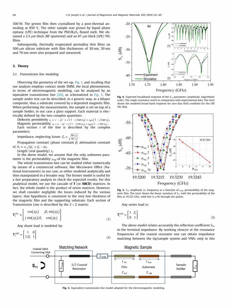
Fig. 4. Expected broadband response of the S11 parameter (amplitude, logarithmicscale). The single resonance notch in comparison with experimental data. The insetshows the modeled broad band response for zero bias field condition for the LPEYIG film.
Fig. 5. S11 amplitude vs. frequency as a function of mmf, permeability of the mag-netic film. The inset shows the linear variation of S11 with the permeability of thefilm at 19.321 GHz, solid line is a fit through the points.
3. Theory
3.1. Transmission line modeling
Observing the geometry of the set-up, Fig. 1, and recalling thatour analysis employs contact mode SMM, the local phenomenon,in terms of electromagnetic modeling, can be analyzed by anequivalent transmission line [20], as schematized in Fig. 3. Thesample under test can be described, in a generic way, as a bilayercomposite, thus a substrate covered by a deposited magnetic film.When performing the measurements, the sample is set on top of asample holder, in our case a glass support. Each material is elec-trically defined by the two complex quantities.
Dielectric permittivity ( ) ( )ε ε ε ε δ ε ε δ= ′ − ″ = ′ − = ′ −j j j1 tan 1 tani e r e0 .Magnetic permeability ( ) ( )μ μ μ μ δ μ μ δ= ′ − ″ = ′ − = ′ −j j j1 tan 1 tani m r m0 .Each section i of the line is described by the complex
parameters:
Impedance, neglecting losses = με
{ }{ }
ZiRe
Rei
i.
Propagation constant (phase constant β, attenuation constantα) ω ε μ β α= = −k ji i i i i.
Length (real quantity) ti.In the above model, we assume that the only unknown para-
meter is the permeability mmf of the magnetic film.The whole transmission line can be studied either numerically
by means of a commercial software, like Microwave Office (Na-tional Instruments) in our case, or either modeled analytically andthen manipulated in a broader way. The former model is useful fora fast preparatory analysis to check the expected results. For thisanalytical model, we use the cascade of T (or ABCD) matrices. Infact, the whole model is the product of seven matrices. However,we shall consider negligible the losses induced by the variouslayers; that hypothesis is consistent to the very low thickness ofthe magnetic film and the supporting substrate. Each section ofTransmission Line is described by the 2�2 matrix:
( ) ( )( ) ( )
β β
β β=
( )
( )⎡
⎣⎢⎢
⎤
⎦⎥⎥
t jZ t
j t Z tT
cos sin
sin / cos 1iTL i i i i i
i i i i i
Any shunt load is modeled by:
=( )
( )⎡⎣⎢
⎤⎦⎥Z
T1 0
1/ 1 2ishl
i
Fig. 3. Equivalent transmission line model ad
Any series load is:
=( )
( )⎡⎣⎢
⎤⎦⎥
ZT
1
0 1 3isel i
The above model relates accurately the reflection coefficient S11to the terminal impedance. By working close/or at the resonancefrequencies of the coaxial resonator one can obtain impedancematching between the tip/sample system and VNA; only in this
opted for the electromagnetic modeling.

Fig. 6. The measured S11 amplitude for the LPE-YIG with respect to different ex-ternal magnetic fields. Inset shows the measured S11 as a function of applied ex-ternal DC magnetic field for the RF sputtered and LPE-YIG samples at the resonancefrequencies.
Fig. 7. Measured S11 response as a function of magnetic field at 17.45 GHz. Thearrows indicate the direction of magnetic field sweep. The inset shows the hys-teresis curve obtained from vibrating sample magnetometer measurement.
C.H. Joseph et al. / Journal of Magnetism and Magnetic Materials 420 (2016) 62–69 65
particular condition, S11 can be approximated as [21]:
≈−+ ( )
SZ ZZ Z 4
total
total11
0
0
Z0 is the characteristic impedance of the system which is 50Ω,
Fig. 8. (a) Measured reflection coefficient for air (empty sample holder), silicon substcondition. (b) Measured S11 variations and resonance frequency as a function of thickne
and = +Z Z Ztotal res sample; Zres is the equivalent impedance of the λ/2coaxial line resonator section, defined as [22]:
ωω= + + +
( )Z Z R j Lj C
1 1 1 15res shunt res res
res
By considering magnetic film and substrate Zsample is a bi-layersystem, defined as:
( )( )=
+
+ ( )Z Z
Z jZ k t
Z jZ k t
tan
tan 6sample mf
sub mf mf mf
mf sub mf mf
where Zsub is the impedance of the substrate and Zmf, kmf and tmf
are the impedance, wave vector and thickness of the magnetic filmrespectively. In our case, with two different kinds of samples (lossydielectric and metallic), the impedance and wave vector of themagnetic film defined as:
( )
( )( )
μ
ε δ
ωμ ε
δ
=−
= + −
( )
⎡⎣⎢
⎤⎦⎥
Zj
k1 tan
and
21 tan 1 ,
for lossy dielectrics YIG 7
mfmf
mf mfmf
mf mfmf
2
( ) ( )( )
π μ ρ π μ ρ= + = +
( )
Z j f k j f1 and 1 / ,
for metals Permalloy 8
mf mf mf mf mf mf
Here mmf, εmf, ρmf and tanδmf are the permeability, permittivity,resistivity and loss tangent of the magnetic film.
3.2. Numerical analysis
Here, we analyze the case of a GGG substrate with a depositedYIG magnetic film (LPE grown YIG with thickness 87 mm). Thelength of the standard coaxial cable connecting the sensing part(tip plus resonator) to the VNA is 105 cm. As the coaxial cablelength is proportional to the loss introduced in the system, weincluded this value in the modeling to obtain the best matchingconditions with respect to the experimental results. The sensingpart is described by the resonator (a coaxial cable of fixed length,with an effective length of 9 cm, and an inner dielectric permit-tivity of 3.72) and a shunt matching load [23], plus the tipequivalent impedance [24] and the cantilever contribution [25].
In the studied case, we vary the permeability mmf of the mag-netic film, keeping geometrical and electromagnetic parametersunchanged. The changing of mmf is expected by means of the var-iation of the intensity of the external magnetic biasing field. In
rate and permalloy films with thicknesses 30 nm, 50 nm and 70 nm at zero biasss of the permalloy film.

Fig. 9. SMM images obtained for bulk permalloy sample at 19.21 GHz. (a) AFM topography image with a scan size of 13 μm�13 μm. (b) Schematic of the bulk sample andarrangement. (c) SMM S11 amplitude image in dB. (d) SMM S11 phase image in degrees. The solid line shows where the profiles of the images has been taken.
C.H. Joseph et al. / Journal of Magnetism and Magnetic Materials 420 (2016) 62–6966
Fig. 4, the inset (1) shows the expected broadband S11 based on ourmodel and in comparison with experimentally obtained S11 re-sponse for the case of air (without sample). The resonator behavesas a band pass filter and shows resonance notches at each 1 GHz,while in Fig. 4 and its inset (2) shows closer look in lower fre-quency region in comparison with experiment data.
It can be observed from Fig. 4 that the experimental resultscannot be completely modeled due to losses and artefacts comingfrom imperfect interconnections in the real setup. Fig. 5 and itsinset show the modeling results of reflection coefficient changes asa function of permeability of the magnetic film. The theory abovesupports the statement that the reflection coefficient S11 decreaseswith increasing permeability. In the practical case, the changes inpermeability will come from the external magnetic bias fieldvariations.
4. Results and discussion
4.1. Spectroscopy
In the experiments, all the measurements were performed incontact mode SMM. As a starting point of the SMM measurement,the frequency sweep from 1 to 20 GHz has been obtained; in asecond step we decided to reduce the frequency bandwidth be-tween 15 GHz and 20 GHz with a step width of 250 kHz, to pro-cure even the smallest variations in the resonance frequency shift.The incident microwave power level was set to 0 dBm and keptthe same for all the measurements. This power level is referred atthe output port of the VNA, and, due to the losses and mismatches,the actual power incident on the sample, can be evaluated,roughly, around 50% of the nominal value, considering the powerdissipation of the shunt matching resistor.

Fig. 10. SMM images obtained for different magnetic bias values (a) H¼0 Oe, (b) H¼225 Oe, (c) 330 Oe, (d) comparison of the profiles of 0 Oe and 225 Oe bias field (e) thetopography and its profile, (f) the S11 variation on the two regions with respect to magnetic bias values. The inset shows a clear variation at 19.75 GHz. The solid lines in theimages represents the place where the profiles have been taken.
C.H. Joseph et al. / Journal of Magnetism and Magnetic Materials 420 (2016) 62–69 67
The measured changes in the amplitude of the reflectioncoefficient S11 with respect to external fields for the RF sputteredand LPE-YIG samples as a function of frequency is shown in Fig. 6.The external magnetic field was applied perpendicular to thesample surface. The inset of Fig. 6 shows the comparison betweenthe LPE and RF sputtered YIG film samples and S11 values as afunction of magnetic field at each resonance frequencies (S11minimum). The LPE sample is more absorptive, as the magneticfield vs amplitude diagram shows a difference of about 1 dBcompared to the RF sputtered film, because of its large thicknessand crystalline nature.
The important point to note here is that S11 changes do notfollow a linear variation with the external magnetic bias field,instead it shows a hysteretic behavior which can be related to themagnetization of the sample. Fig. 7 shows the hysteresis behaviorof S11 with respect to the external magnetic field and the insetshows the hysteresis curve obtained from vibrating sample mag-netometer (VSM) data. The measured in-plane coercivity for LPEand RF sputtered YIG films from the VSM measurements are253.29 Oe and 404.13 Oe and the magnetization values are
0.168 emu and 22.66�10�3 emu respectively.Similarly, the reflection coefficient changes have been analyzed
for the permalloy thin films having different thicknesses. Fig. 8(a) shows the resonance notches for the cases of air (empty sampleholder), pure silicon substrate and permalloy films with thethicknesses of 30 nm, 50 nm and 70 nm. From Eq. (6), we knowthat the changes in the thickness of the film will change the totalimpedance of the system, which results in observing changes inS11. Fig. 8(b) shows the changes in S11 and the shift in the re-sonance frequency with respect to the thickness of the permalloyfilm. It also shows that the 70 nm thick film has large change in S11compared to 30 and 50 nm and this change also related to thesurface quality of the film with the increase in thickness.
4.2. Imaging
Fig. 9 shows the obtained SMM image of bulk permalloy sam-ple surface. The image has been acquired after the selection ofsingle frequency at 19.21 GHz close to a resonance notch from thefrequency sweep of 15–20 GHz. The IF band width was kept at

Fig. 11. The SMM images obtained at 19.94 GHz for the LPE-YIG sample with respect to different external magnetic fields. (a) Topography image with a scan size of10 μm�10 μm. (b) S11 amplitude image in dB for zero magnetic bias, (c) H¼500 Oe, (d) H¼1000 Oe, and (d) H¼1500 Oe. The black solid line shows where the profiles of theimages have been taken.
C.H. Joseph et al. / Journal of Magnetism and Magnetic Materials 420 (2016) 62–6968
500 Hz for all the images and the scan speed was 21.54 mm/s andalso the image obtained without external magnetic bias condition.Fig. 9(a) shows the topography image and Fig. 9(b) shows theschematic of the bulk sample and the arrangement. Fig. 9(c) and(d) show the amplitude and the phase of the recorded S11 signal.The topography shows locally a smooth surface but the amplitudeand phase images are showing two distinct regions with largechanges in S11 signal between them of about 2 dB in amplitudeand more than 10° changes in the phase signal. The profiles areshowing the variations along the solid line in the images whichgoes through the two regions. The variations are clearly visible inS11 signal when comparing these results to the topographicalvariations. This is a visible evidence that those two regions exhibittwo different magnetization properties on the surface of thesample. In order to see the variations with respect to the externalbias field H, different fields of values 225 Oe (Fig. 10(b)) and 330 Oe(Fig. 10(c)) have been applied perpendicularly to the samplesurface.
Fig. 10(a) shows the image of bulk permalloy sample surfacewithout any bias field. Fig. 10(b) as well as (c) shows the imageswith external field values of 225 Oe and 330 Oe, respectively.Fig. 10(e) shows the topography and its profile, which clearly in-dicates that there is no topographic variation and no distinct re-gions like in the case of S11 signal. The images are showing that thevariations with respect to external field are not high, but a verysmall change of about 0.08 dB from 0 Oe to 225 Oe and about0.28 dB when changing the magnetic field from 225 Oe to 330 Oe.Fig. 10(d) shows the comparison of the profiles of zero bias
condition and 225 Oe bias field condition and it shows the im-provement in differentiating the two regions when applying ex-ternal bias field. As the changes observed in the images are ex-tremely sensible when applying external fields, we have alsoperformed single point spectroscopy measurements on the tworegions. To improve the signal to noise ratio, 30 dB amplificationhas been provided using the Dopant Profiling MeasurementModule (DPMM, Keysight Technology). Fig. 10(f) shows the fre-quency sweep response of the two regions with respect to dif-ferent bias fields. The inset shows a clear picture of the variationsin both regions with respect to the bias magnetic field. This is anindication that the magnetic properties on the two regions arechanging with the external field.
Fig. 11 shows the images obtained for the LPE-YIG film sample.Fig. 11(a) shows the topography containing some grains of averagediameter of 1.5 μm. In order to demonstrate the magnetic prop-erties changes on the surface of the sample, we swept the mag-netic bias field: (b) 0 Oe, (c) 500 Oe, (d) 1000 Oe and (e) 1500 Oe. Itis clearly visible, when increasing the magnetic bias value fromzero, the surface becomes more absorptive and this effect resultsin a decrease of S11 amplitude with an increase in magnetic bias.Fig. 11(f) shows the profiles of the single grain absorption withmagnetic bias field. This is evidently an indication that the changesin the impedance of the tip/sample system come only from thechanges in magnetic properties, i.e. from the inductive part of theimpedance, but not from any capacitive changes. Actually, themagnetic bias will not produce any alterations in the capacitancepart, which is related to the dielectric constant of the material and

C.H. Joseph et al. / Journal of Magnetism and Magnetic Materials 420 (2016) 62–69 69
not to the magnetic permeability.
5. Conclusions
We have demonstrated the capability of a scanning microwavemicroscope (SMM) system of characterizing thin and bulk mag-netic materials. Specifically, we tested the response of magneticgarnets and permalloy samples looking for imaging and micro-wave spectroscopy in terms of reflection measurements. Qualita-tive and quantitative results have been discussed, with evidencefor the change of the microwave absorption of the material undertest when biased by means of a DC magnetic field orthogonal tothe surface. The versatility proper of the SMM allows for both afast, large area, characterization of the sample's magnetic prop-erties in imaging mode, and also for point-wise spectroscopymode, which provides higher accuracy and sensitivity of theminute changes in the measured parameters. In fact, the SMM tipacts as a local antenna, able to detect very small changes of thephase and amplitude of the reflected signal. An equivalent elec-tromagnetic transmission line model of the interaction betweenthe tip and the sample has also been proposed, to be evolved forcalibration purposes and for quantitative analysis of the localpermeability. We also observed the hysteretic behavior of the re-flection coefficient S11 with the external bias field. In comparisonwith vibrating sample magnetometry (VSM), which is a non-localmeasurement, SMM can provide a frequency dependent localhysteresis plot. In conclusion, exploiting the nanoscale potentialityof the measurement system, highly localized measurements atmicrowave frequencies can be performed, very useful in thecharacterization of materials and devices exhibiting respectivelymagnetic nanoscale response and details.
Acknowledgments
The authors are highly thankful to Giorgio Badino from Key-sight Technologies (Austria) for helping in carrying out SMMmeasurements. The authors would like to thank Loukas Michalasfrom CNR-IMM Rome (Italy) for helpful technical discussions. Theauthors also wish to thank Muthukumaran from IIT Madras (India)for VSM measurements. The authors wish to acknowledge thesupport from European Commission for “Marie Curie” researchfellowship in the framework of PEOPLE-2012-ITN project: Micro-wave Nanotechnology for Semiconductor and Life Science -NA-NOMICROWAVE, under GA: 317116.
References
[1] S.M. Anlage, V.V. Talanov, A.R. Schwartz, Principle of near field microwavemicroscopy, in: Scanning Probe Microscopy: Electrical and ElectromechanicalPhenomena at the Nanoscale, Springer-Verlag, 2007, pp. 215–253.
[2] B.T. Rosner, D.W. van der Weide, High-frequency near-field microscopy, Rev.Sci. Instrum. 73 (2) (2002) 2505–2525.
[3] A. Imtiaz, T.M. Wallis, P. Kabos, Near-field scanning microwave microscopy: anemerging research tool for nanoscale metrology, IEEE Microw. Mag. 15 (1)
(2014) 52–64.[4] V.V. Talanov, A.R. Schwartz, Near-field scanning microwave microscope for
interline capacitance characterization of nanoelectronics interconnect, IEEETrans. Microw. Theory Tech. 57 (5) (2009) 1224–1229.
[5] V.V. Talanov, C. Del Barga, L. Wickey, I. Kalichava, E. Gonzales, E. Shaner, A. Gin,N. Kalugin, Few-layer graphene characterization by near-field scanning mi-crowave microscopy, ACS Nano 4 (2010) 3831–3838.
[6] A. Tselev, Nickolay V. Lavrik, Ivan Vlassiouk, Dayrl P. Brigg1, Maarten Rutgers,Roger Proksch, Sergei V. Kalinin, Near-field microwave scanning probe ima-ging of conductivity inhomogeneities in CVD graphene, Nanotechnology 23(385706) (2012) 11.
[7] G. Gramse, E. Brinciotti, A. Lucibello, S.B. Patil, M. Kasper, C. Rankl,R. Giridharagopal, P. Hinterdorfer, R. Marcelli, F. Kienberger, Quantitative sub-surface and non-contact imaging using scanning microwave microscopy, Na-notechonology 26 (2015) 135701.
[8] G. Gramse, M. Kasper, L. Fumagalli, G. Gomila, P. Hinterdorfer, F. Kienberger,Calibrated complex impedance and permittivity measurements with scanningmicrowave microscopy, Nanotechnology 25 (14) (2014) 145703.
[9] L. Michalas, E. Brinciotti, A. Lucibello, G. Gramse, C.H. Joseph, F. Kienberger,E. Proietti, R. Marcelli, De-embedding techniques for nanoscale characteriza-tion of semiconductors by scanning microwave microscopy, Microelectron.Eng. 159 (2016) 64–69.
[10] E. Brinciotti, G. Gramse, S. Hommel, T. Schweinboeck, A. Altes, M.A. Fenner,J. Smoliner, M. Kasper, G. Badino, S.-S. Tuca, F. Kienberger, Probing resistivityand doping concentration of semiconductors at the nanoscale using scanningmicrowave microscopy, Nanoscale 7 (2015) 14715.
[11] J. Park, S. Hyun, A. Kim, t Kim, K. Char, Observation of biological samples usinga scanning microwave microscope, Ultramicroscopy 102 (2005) 101–106.
[12] M.C. Biagi, R. Fabregas, G. Gramse, M. Van Der Hofstadt, A. Juárez,F. Kienberger, L. Fumagalli, G. Gomila, Nanoscale electric permittivity of singlebacterial cells at gigahertz frequencies by scanning microwave microscopy,ACS Nano 10 (1) (2016) 280–288.
[13] S.-S. Tuca, G. Badino, G. Gramse, E. Brinciotti, M. Kasper, Y.J. Oh, C. Rankl,P. Hinterdorfer, F. Kienberger, Calibrated complex impedance of CHO cells andE. Coli bacteria at GHz frequencies using scanning microwave microscopy,Nanotechnology 27 (2016) 135702.
[14] G. Srinivasan, A.S. Tatarenko, M.I. Bichurin, Electrically tunable microwavefilters based on ferromagnetic resonance in ferrite-ferroelectric bilayers,Electron. Lett. 41 (10) (2005) 596–598.
[15] Yu. V. Gulyaev, S.A. Nikitov, L.V. Zhivotovskii, A.A. Klimov, Ph Tailhades,L. Presmanes, C. Bonningue, C.S. Tsai, S.L. Vysotskii, Yu. A. Filimonov, Ferro-magnetic films with magnon bandgap periodic structures: magnon crystals, J.Exp. Theor. Phys. Lett. 77 (10) (2003) 567–570.
[16] R. Marcelli, G. Sajin, A. Cismaru, F. Craciunoiu, Band-stop magnetostatic wavesmicromachined resonators, Appl. Phys. Lett. 84 (2004) 2445.
[17] H. Melikyan, A. Hovsepyan, T. Sargsyan, Y. Yoon, H. Yoo, A. Babajanyan, K. Lee,Characterization of magnetic materials using a scanning microwave microp-robe, Ultramicroscopy 108 (2008) 1030–1033.
[18] S.C. Lee, C.P. Vlahacos, B.J. Feenstra, A. Schwartz, D.E. Steinhauer, F.C. Wellstood, S.M. Anlage, Magnetic permeability imaging of metals with ascanning near-field microwave microscope, Appl. Phys. Lett. 77 (2000) 4404.
[19] H. Melikyan, T. Sargsyan, A. Babajanyan, S. Kim, J. Kim, K. Lee, B. Friedman,Hard disk magnetic domain nano-spatial resolution imaging by using a near-field scanning microwave microscope with an AFM probe tip, J. Magn. Magn.Mater. 321 (2009) 2483–2487.
[20] D.M. Pozar, Microwave Engineering, 3rd ed., Wiley 2004, pp. 49–84.[21] K. Lee, H. Melikyan, A. Babajanyan, B. Friedman, Near-field microwave mi-
croscopy for nanoscience and nanotechnology, in: Scanning Probe Microscopyin Nanoscience and Nanotechnology, volume 2, Springer, 2010, pp. 135–169.
[22] G.M. Sardi, A. Lucibello, M. Kasper, G. Gramse, E. Proietti, F. Kienberger,R. Marcelli, Optimization of the imaging response of scanning microwavemicroscopy measurements, Appl. Phys. Lett. 107 (3) (2015) 033107.
[23] K. Torigoe, M. Arita, T. Motooka, Sensitivity analysis of scanning microwavemicroscopy for nano-scale dopant measurement in Si, J. Appl. Phys. 112 (2012)104325.
[24] A.O. Oladipo, M. Kasper, S. Lavdas, G. Gramse, F. Kienberger, N.C. Panoiu,Three-dimensional finite-element simulations of a scanning microwave mi-croscope cantilever for imaging at the nanoscale, Appl. Phys. Lett. 103 (21)(2013) 213106.
[25] G. Bartolucci, G.M. Sardi, R. Marcelli, E. Proietti, A. Lucibello, E. Stoja, F. Frezza,Modeling of a metallic truncated cone for electromagnetic capacitive sensors,J. Appl. Phys. 118 (7) (2015) 074503.