Embed Size (px)
Citation preview
Journal ofMaterials Chemistry A
PAPER
Publ
ishe
d on
09
Dec
embe
r 20
15. D
ownl
oade
d by
Fud
an U
nive
rsity
on
24/0
1/20
16 0
6:07
:09.
View Article OnlineView Journal | View Issue
Uniform carbon-
aDepartment of Materials Science, Fudan U
E-mail: [email protected] of Chemistry and Biochemistr
California 95064, USA. E-mail: zhang@ucsc
† Electronic supplementary informa10.1039/c5ta09024e
Cite this: J. Mater. Chem. A, 2016, 4,1078
Received 8th November 2015Accepted 7th December 2015
DOI: 10.1039/c5ta09024e
www.rsc.org/MaterialsA
1078 | J. Mater. Chem. A, 2016, 4, 1078
coated CdS core–shellnanostructures: synthesis, ultrafast charge carrierdynamics, and photoelectrochemical watersplitting†
Sancan Han,a Ying-Chih Pu,b Lingxia Zheng,a Linfeng Hu,a Jin Zhong Zhang*b
and Xiaosheng Fang*a
Photoelectrochemical (PEC) water splitting using solar energy has received widespread attention, and
strong performance photocatalysts are highly desired. In this work, uniform carbon-coated CdS
nanostructures have been fabricated using ascorbic acid as the carbon source by a facile hydrothermal
method and characterized using transmission electron microscopy (TEM). The thickness of the carbon
layer can be well controlled by the amount of ascorbic acid added during the reaction. Compared to
pristine CdS, carbon-coated CdS nanostructures exhibit stronger light absorption and more efficient
electron transfer as determined by absorption and photoluminescence (PL) spectroscopy. Ultrafast
charge carrier dynamics in the composite CdS/C structures were studied using femtosecond transient
absorption (TA) spectroscopy, which revealed direct evidence of effective charge transfer from CdS to
the carbon layer. In addition, the CdS/C composites were employed as photoanodes for PEC hydrogen
generation, which showed significant improvement in photoactivity over pristine CdS nanospheres. The
photocurrent density (�1.0 V vs. Ag/AgCl) of one of the composite structures, CdS/7-C, exhibited �20
times enhancement compared with that of pristine CdS. The enhanced PEC property can be attributed
to increased light scattering and consequently the light harvesting throughout the whole spectral
wavelength, and the effective electron transfer from CdS to the carbon layer. Such carbon-coated
semiconductor composites based on a simple and low-cost synthesis method should be useful in PEC
as well as other applications such as photovoltaics, detectors and sensors.
1. Introduction
Water splitting utilizing solar energy has been a topic of stronginterest in the eld of renewable energy. In particular, photo-electrochemical (PEC) water splitting using nanoscaled semi-conductor photocatalysts has received signicant attention.1–6
Among them, cadmium sulde (CdS) with a direct bandgap of�2.4 eV has absorption matching well with the spectrum ofsunlight and also owing to its other useful properties such asexcellent charge carrier transport, relatively low work function,good chemical and thermal stability is considered as an excel-lent material for PEC applications.7–12 Despite these advantages,one limitation is its generally low PEC conversion efficienciesdue to fast charge carrier recombination. Therefore, mucheffort has been made to effectively reduce recombination of
niversity, Shanghai 200433, P. R. China.
y, University of California, Santa Cruz,
.edu
tion (ESI) available. See DOI:
–1086
charge carriers.13–16 For example, Wu et al. have demonstratedthat a CdS–Pt heterostructure can provide a possible way foroptimizing the hole transfer step to achieve efficient solar-to-fuel conversion.17 Li et al. reported that the combination ofenhanced charge transfer and broad light absorption wasresponsible for improved hydrogen generation in the sandwich-structured CdS–Au–TiO2 nanorod arrays as photoanodes inPEC.18 However, these semiconductor-layers and plasmonic-metal layers (mainly silver and gold) tend to self-agglomerate,which increases the recombination of electrons and holes.
Carbon materials exhibit excellent electrical conductivity,19
superior chemical and electrochemical stability,20 uniquephysical properties,21 and good light response.22 Intense studieshave been focused on graphene/semiconductor composites inphotocatalytic and PEC applications.13,23–29 However, completeand uniform graphene coverage on the semiconductor, whichensures electron transfer in all directions, has been challengingfor practical application. Meanwhile, carbon-coated semi-conductors with complete and ultrathin carbon layers havebeen extensively investigated in lithium-ion batteries and pho-tocatalysis,30–33 Lou et al. have rstly evidenced that a carbon-
This journal is © The Royal Society of Chemistry 2016
Paper Journal of Materials Chemistry A
Publ
ishe
d on
09
Dec
embe
r 20
15. D
ownl
oade
d by
Fud
an U
nive
rsity
on
24/0
1/20
16 0
6:07
:09.
View Article Online
coated CdS nanohybrid exhibits signicantly enhanced photo-stability and photocatalytic ability,33 indicating that thin carbonlayers with a degree of graphitization can facilitate electrontransfer and prevent the active core materials from contactingwith oxygen and moisture in the air. This suggests that carbonlayers should be an ideal and promising shell material forcoating active semiconductor photocatalysts in PEC applica-tions. However, the report about carbon-coated semiconductorsapplied for a photoelectrochemical eld is scarce. Moreover, todate there are mainly two methods for depositing carbonlayers:34,35 (1) in situ pyrolysis of the organic precursor (e.g.glucose and citric acid); (2) a chemical vapor deposition (CVD)assisted solid-state route. However, these two approachesusually lead to partial carbon coating or require high tempera-ture annealing (>600 �C) under an inert atmosphere. Therefore,a simple, efficient and low-cost method for the deposition ofuniform carbon-coated semiconductors at mild operationtemperature is highly desired.
In this work, CdS/C composites were synthesized in highyields using ascorbic acid as the carbon source by a facile two-step hydrothermal method, which produces a uniform, thincarbon layer coating on the CdS surface. The thickness of thecarbon layer can be easily controlled by the amount of ascorbicacid in the reaction. The effective electron transfer and morelight absorption in CdS/C composites are conrmed by PL, andUV-vis spectroscopy, which could lead to the enhanced photo-activity. According to the PEC study, the carbon-coated CdSelectrode indeed shows excellent photoactivity compared withthat of pristine CdS. Importantly, the role of the carbon layer oncharge carrier dynamics in detail has been investigated usingfemtosecond transient absorption (TA) spectroscopy, whichprovides a direct measure of charge carrier dynamics includingelectron transfer from CdS to the carbon layer. These resultsshow that a uniform and thin layer of carbon material cansubstantially enhance electron transfer, which leads to thesignicant enhancement in the photocurrent density comparedwith that of pristine CdS. Hence, the CdS/C core–shellcomposites obtained provide promising candidates for highperformance PEC and other potential applications, and thefacile and low-cost synthetic method can be extended to fabri-cate other carbon-coated semiconductors.
2. Experimental section2.1 Materials
All chemicals were used as received without any further puri-cation. Cd(CH3COO)2$2H2O (Sinopharm Chemical ReagentCorp.), thiourea (Sinopharm Chemical Reagent Corp.), analyticalcohol (98%, Sigma-Aldrich), and ascorbic acid (SinopharmChemical Reagent Corp.).
2.2 Synthesis of CdS/C composites
The synthesis of pristine CdS nanospheres. The CdS nano-spheres were fabricated by a modied method described indetail elsewhere.12 Typically, 2.4 mmol of Cd(CH3COO)2$2H2Oand 24 mmol of thiourea in 60 mL deionized water, were added
This journal is © The Royal Society of Chemistry 2016
to a 100 mL Teon-lined stainless steel autoclave, then theautoclave was maintained at 200 �C for 5 h and allowed to coolto room temperature naturally aerwards. Yellow precipitateswere collected and washed with deionized water and ethanolthree times, respectively. The nal products were dried ina vacuum oven at 65 �C for 10 h.
The synthesis of CdS/C composites. Pristine CdS nano-spheres in 30 mL de-ionized water and 30 mL ethanol werestirred for 1 hour. Ascorbic acid was added into the solution tostir for another 1 h, and then it was transferred to a 100 mLTeon-lined stainless steel autoclave to maintain the tempera-ture at 200 �C for 2 h and cooled down naturally to roomtemperature. Then the samples were collected by centrifugationand washed with deionized water and ethanol for several times,respectively. The nal products were dried in a vacuum oven for8 h at 60 �C. The pure carbon materials were fabricated withoutCdS for comparison under the same reaction conditions.
2.3 Characterization
The morphology and the carbon layer thickness were deter-mined by high-resolution transmission electron microscopy(HR-TEM, TECNAI G2 S-TWIN). X-ray diffraction using Cu Karadiation (XRD, Bruker D8-A25) was adopted to examine thecrystalline structure of the samples. The optical and uores-cence properties of the samples at room temperature wereinvestigated using a UV-vis spectrophotometer (Hitachi U-4100)and photoluminescence (PL) spectrouorometer (Fluoromax-4).The XPS spectra of the samples were recorded with a PerkinElmer PHI 5000 C ESCA system equipped with a hemisphericalelectron energy analyzer, and the Mg-Ka (1253.6 eV) anode wasoperated at 14 kV and 20 mA. The FT-IR and Raman spectrawere collected on a Nexus 470 FT-IR spectrometer and Spex 403Raman spectrometer.
Ultrafast transient absorption (TA) spectroscopy was carriedout with a Quantronix laser system consisting of a Palitra-FSoptical parametric amplier pumped by an Integra-C Ti:sap-phire amplier system, as reported in the previous work.36
Briey, 795 nm, 820 mW, and 150 fs pulses from Integra-C weresplit 9 : 1 between an optical parametric amplier (OPA) andsapphire crystal, respectively. A pump wavelength of 400 nm(�3.1 eV) was used to excite the samples at 90 nJ per pulse,which could guarantee linear effects. And a white lightcontinuum, which was stable from 430 nm to 800 nm witha pulse width of 100 fs, was used to probe the samples.
2.4 Photoelectrochemical test
The photocurrent of pristine CdS and CdS/C composites elec-trodes was measured using a Solartron 1280 B (Oakridge, TN)electrochemical workstation in a three-electrode electro-chemical cell with a Pt wire as the counter electrode and Ag/AgCl as a reference electrode. In a typical experiment, thepotential was swept from �1.2 V to 0 V vs. Ag/AgCl at a scan rateof 5 mV s�1. IPCE were measured using a xenon lamp (1000 W)coupled with an infrared water lter (Oriel 6127) and alignedmonochromator (Oriel Cornerstone 130 1/8m). The sampleswere spun on the Fluorine-doped Tin Oxide (FTO) glass (7 U
J. Mater. Chem. A, 2016, 4, 1078–1086 | 1079
Journal of Materials Chemistry A Paper
Publ
ishe
d on
09
Dec
embe
r 20
15. D
ownl
oade
d by
Fud
an U
nive
rsity
on
24/0
1/20
16 0
6:07
:09.
View Article Online
sq�1) and then annealed at 350 �C for 2 h under a nitrogenenvironment, used as the working electrode with a working areaof (�1 cm2). A 0.25 M Na2S and 0.35 Na2SO3 aqueous solutionwas used as the electrolyte.
3. Results and discussion
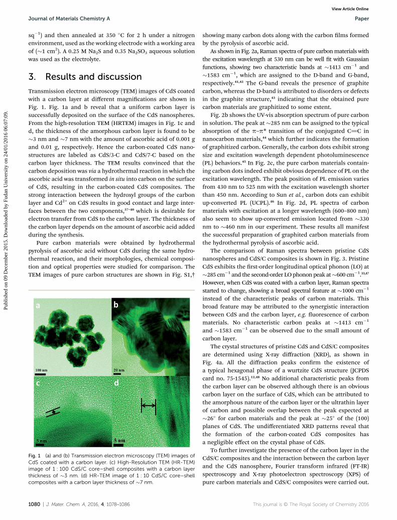
Transmission electron microscopy (TEM) images of CdS coatedwith a carbon layer at different magnications are shown inFig. 1. Fig. 1a and b reveal that a uniform carbon layer issuccessfully deposited on the surface of the CdS nanospheres.From the high-resolution TEM (HRTEM) images in Fig. 1c andd, the thickness of the amorphous carbon layer is found to be�3 nm and �7 nm with the amount of ascorbic acid of 0.001 gand 0.01 g, respectively. Hence the carbon-coated CdS nano-structures are labeled as CdS/3-C and CdS/7-C based on thecarbon layer thickness. The TEM results convinced that thecarbon deposition was via a hydrothermal reaction in which theascorbic acid was transformed in situ into carbon on the surfaceof CdS, resulting in the carbon-coated CdS composites. Thestrong interaction between the hydroxyl groups of the carbonlayer and Cd2+ on CdS results in good contact and large inter-faces between the two components,37–40 which is desirable forelectron transfer from CdS to the carbon layer. The thickness ofthe carbon layer depends on the amount of ascorbic acid addedduring the synthesis.
Pure carbon materials were obtained by hydrothermalpyrolysis of ascorbic acid without CdS during the same hydro-thermal reaction, and their morphologies, chemical composi-tion and optical properties were studied for comparison. TheTEM images of pure carbon structures are shown in Fig. S1,†
Fig. 1 (a) and (b) Transmission electron microscopy (TEM) images ofCdS coated with a carbon layer. (c) High-Resolution TEM (HR-TEM)image of 1 : 100 CdS/C core–shell composites with a carbon layerthickness of �3 nm. (d) HR-TEM image of 1 : 10 CdS/C core–shellcomposites with a carbon layer thickness of �7 nm.
1080 | J. Mater. Chem. A, 2016, 4, 1078–1086
showing many carbon dots along with the carbon lms formedby the pyrolysis of ascorbic acid.
As shown in Fig. 2a, Raman spectra of pure carbonmaterials withthe excitation wavelength at 530 nm can be well t with Gaussianfunctions, showing two characteristic bands at �1413 cm�1 and�1583 cm�1, which are assigned to the D-band and G-band,respectively.41,42 The G-band reveals the presence of graphitecarbon, whereas the D-band is attributed to disorders or defectsin the graphite structure,43 indicating that the obtained purecarbon materials are graphitized to some extent.
Fig. 2b shows the UV-vis absorption spectrum of pure carbonin solution. The peak at �285 nm can be assigned to the typicalabsorption of the p–p* transition of the conjugated C]C innanocarbon materials,44 which further indicates the formationof graphitized carbon. Generally, the carbon dots exhibit strongsize and excitation wavelength dependent photoluminescence(PL) behaviors.45 In Fig. 2c, the pure carbon materials contain-ing carbon dots indeed exhibit obvious dependence of PL on theexcitation wavelength. The peak position of PL emission variesfrom 430 nm to 525 nm with the excitation wavelength shorterthan 450 nm. According to Sun et al., carbon dots can exhibitup-converted PL (UCPL).46 In Fig. 2d, PL spectra of carbonmaterials with excitation at a longer wavelength (600–800 nm)also seem to show up-converted emission located from �330nm to �460 nm in our experiment. These results all manifestthe successful preparation of graphited carbon materials fromthe hydrothermal pyrolysis of ascorbic acid.
The comparison of Raman spectra between pristine CdSnanospheres and CdS/C composites is shown in Fig. 3. PristineCdS exhibits the rst-order longitudinal optical phonon (LO) at�285 cm�1 and the second-order LOphonon peak at�600 cm�1.33,47
However, when CdS was coated with a carbon layer, Raman spectrastarted to change, showing a broad spectral feature at �1000 cm�1
instead of the characteristic peaks of carbon materials. Thisbroad feature may be attributed to the synergistic interactionbetween CdS and the carbon layer, e.g. uorescence of carbonmaterials. No characteristic carbon peaks at �1413 cm�1
and �1583 cm�1 can be observed due to the small amount ofcarbon layer.
The crystal structures of pristine CdS and CdS/C compositesare determined using X-ray diffraction (XRD), as shown inFig. 4a. All the diffraction peaks conrm the existence ofa typical hexagonal phase of a wurtzite CdS structure (JCPDScard no. 75-1545).12,48 No additional characteristic peaks fromthe carbon layer can be observed although there is an obviouscarbon layer on the surface of CdS, which can be attributed tothe amorphous nature of the carbon layer or the ultrathin layerof carbon and possible overlap between the peak expected at�26� for carbon materials and the peak at �25� of the (100)planes of CdS. The undifferentiated XRD patterns reveal thatthe formation of the carbon-coated CdS composites hasa negligible effect on the crystal phase of CdS.
To further investigate the presence of the carbon layer in theCdS/C composites and the interaction between the carbon layerand the CdS nanosphere, Fourier transform infrared (FT-IR)spectroscopy and X-ray photoelectron spectroscopy (XPS) ofpure carbon materials and CdS/C composites were carried out.
This journal is © The Royal Society of Chemistry 2016
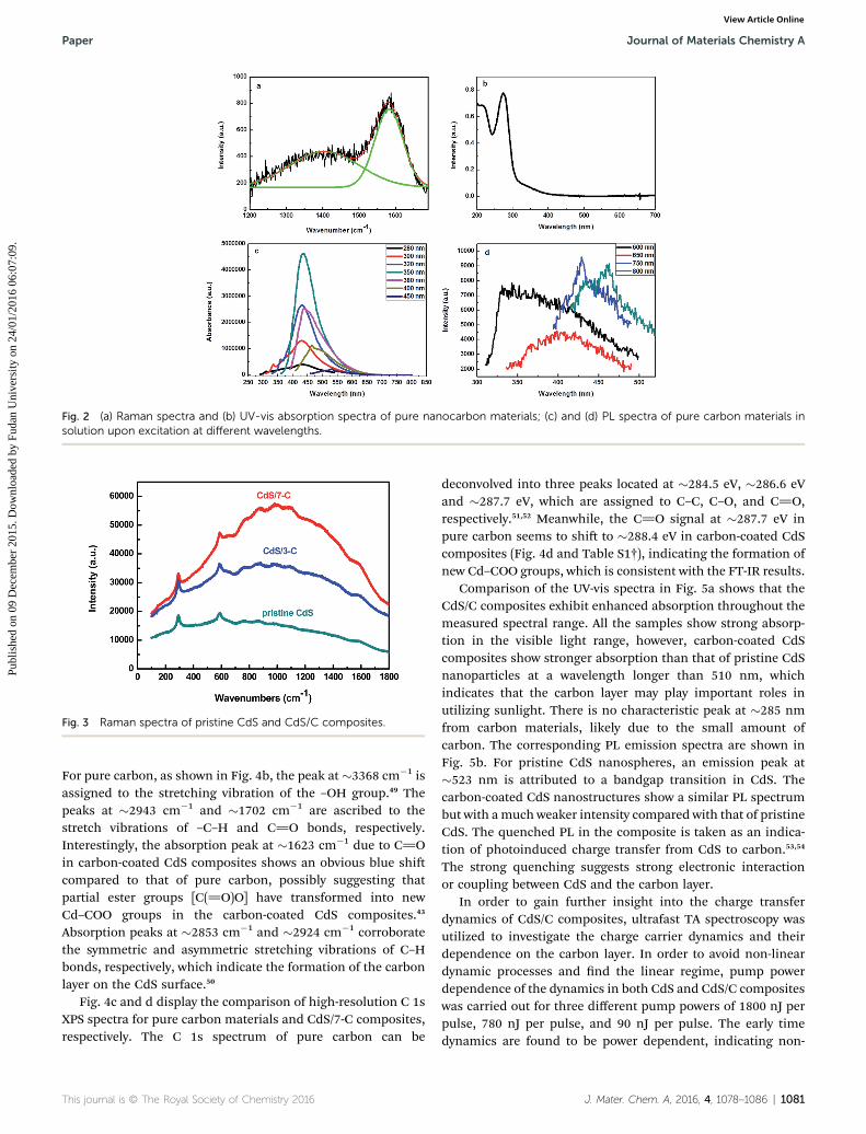
Fig. 2 (a) Raman spectra and (b) UV-vis absorption spectra of pure nanocarbon materials; (c) and (d) PL spectra of pure carbon materials insolution upon excitation at different wavelengths.
Fig. 3 Raman spectra of pristine CdS and CdS/C composites.
Paper Journal of Materials Chemistry A
Publ
ishe
d on
09
Dec
embe
r 20
15. D
ownl
oade
d by
Fud
an U
nive
rsity
on
24/0
1/20
16 0
6:07
:09.
View Article Online
For pure carbon, as shown in Fig. 4b, the peak at�3368 cm�1 isassigned to the stretching vibration of the –OH group.49 Thepeaks at �2943 cm�1 and �1702 cm�1 are ascribed to thestretch vibrations of –C–H and C]O bonds, respectively.Interestingly, the absorption peak at �1623 cm�1 due to C]Oin carbon-coated CdS composites shows an obvious blue shicompared to that of pure carbon, possibly suggesting thatpartial ester groups [C(]O)O] have transformed into newCd–COO groups in the carbon-coated CdS composites.43
Absorption peaks at �2853 cm�1 and �2924 cm�1 corroboratethe symmetric and asymmetric stretching vibrations of C–Hbonds, respectively, which indicate the formation of the carbonlayer on the CdS surface.50
Fig. 4c and d display the comparison of high-resolution C 1sXPS spectra for pure carbon materials and CdS/7-C composites,respectively. The C 1s spectrum of pure carbon can be
This journal is © The Royal Society of Chemistry 2016
deconvolved into three peaks located at �284.5 eV, �286.6 eVand �287.7 eV, which are assigned to C–C, C–O, and C]O,respectively.51,52 Meanwhile, the C]O signal at �287.7 eV inpure carbon seems to shi to �288.4 eV in carbon-coated CdScomposites (Fig. 4d and Table S1†), indicating the formation ofnew Cd–COO groups, which is consistent with the FT-IR results.
Comparison of the UV-vis spectra in Fig. 5a shows that theCdS/C composites exhibit enhanced absorption throughout themeasured spectral range. All the samples show strong absorp-tion in the visible light range, however, carbon-coated CdScomposites show stronger absorption than that of pristine CdSnanoparticles at a wavelength longer than 510 nm, whichindicates that the carbon layer may play important roles inutilizing sunlight. There is no characteristic peak at �285 nmfrom carbon materials, likely due to the small amount ofcarbon. The corresponding PL emission spectra are shown inFig. 5b. For pristine CdS nanospheres, an emission peak at�523 nm is attributed to a bandgap transition in CdS. Thecarbon-coated CdS nanostructures show a similar PL spectrumbut with amuch weaker intensity compared with that of pristineCdS. The quenched PL in the composite is taken as an indica-tion of photoinduced charge transfer from CdS to carbon.53,54
The strong quenching suggests strong electronic interactionor coupling between CdS and the carbon layer.
In order to gain further insight into the charge transferdynamics of CdS/C composites, ultrafast TA spectroscopy wasutilized to investigate the charge carrier dynamics and theirdependence on the carbon layer. In order to avoid non-lineardynamic processes and nd the linear regime, pump powerdependence of the dynamics in both CdS and CdS/C compositeswas carried out for three different pump powers of 1800 nJ perpulse, 780 nJ per pulse, and 90 nJ per pulse. The early timedynamics are found to be power dependent, indicating non-
J. Mater. Chem. A, 2016, 4, 1078–1086 | 1081
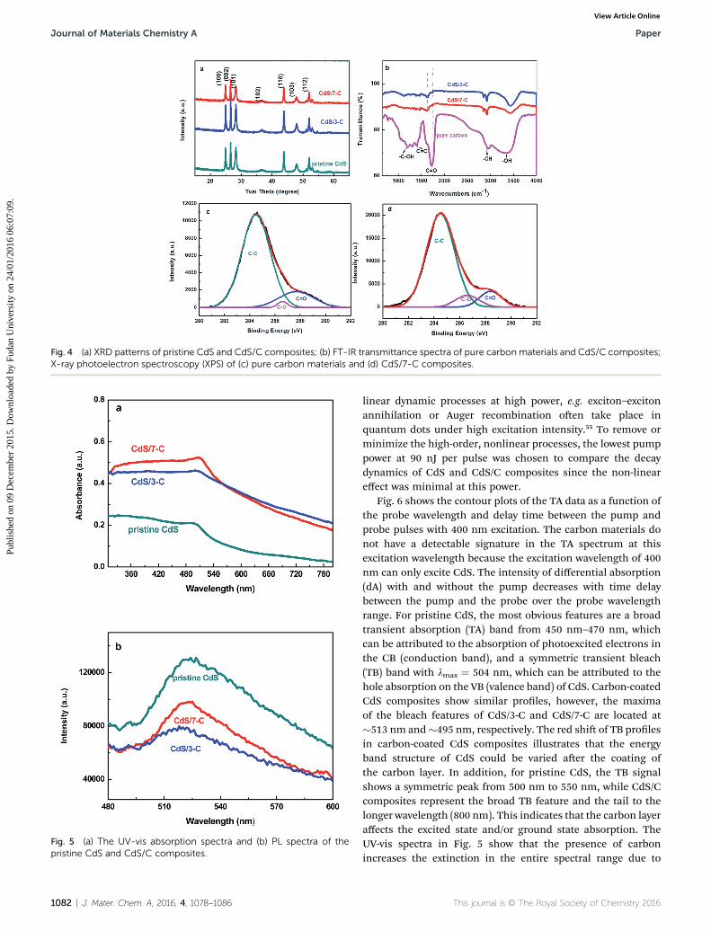
Fig. 4 (a) XRD patterns of pristine CdS and CdS/C composites; (b) FT-IR transmittance spectra of pure carbon materials and CdS/C composites;X-ray photoelectron spectroscopy (XPS) of (c) pure carbon materials and (d) CdS/7-C composites.
Fig. 5 (a) The UV-vis absorption spectra and (b) PL spectra of thepristine CdS and CdS/C composites.
1082 | J. Mater. Chem. A, 2016, 4, 1078–1086
Journal of Materials Chemistry A Paper
Publ
ishe
d on
09
Dec
embe
r 20
15. D
ownl
oade
d by
Fud
an U
nive
rsity
on
24/0
1/20
16 0
6:07
:09.
View Article Online
linear dynamic processes at high power, e.g. exciton–excitonannihilation or Auger recombination oen take place inquantum dots under high excitation intensity.55 To remove orminimize the high-order, nonlinear processes, the lowest pumppower at 90 nJ per pulse was chosen to compare the decaydynamics of CdS and CdS/C composites since the non-lineareffect was minimal at this power.
Fig. 6 shows the contour plots of the TA data as a function ofthe probe wavelength and delay time between the pump andprobe pulses with 400 nm excitation. The carbon materials donot have a detectable signature in the TA spectrum at thisexcitation wavelength because the excitation wavelength of 400nm can only excite CdS. The intensity of differential absorption(dA) with and without the pump decreases with time delaybetween the pump and the probe over the probe wavelengthrange. For pristine CdS, the most obvious features are a broadtransient absorption (TA) band from 450 nm–470 nm, whichcan be attributed to the absorption of photoexcited electrons inthe CB (conduction band), and a symmetric transient bleach(TB) band with lmax ¼ 504 nm, which can be attributed to thehole absorption on the VB (valence band) of CdS. Carbon-coatedCdS composites show similar proles, however, the maximaof the bleach features of CdS/3-C and CdS/7-C are located at�513 nm and�495 nm, respectively. The red shi of TB prolesin carbon-coated CdS composites illustrates that the energyband structure of CdS could be varied aer the coating ofthe carbon layer. In addition, for pristine CdS, the TB signalshows a symmetric peak from 500 nm to 550 nm, while CdS/Ccomposites represent the broad TB feature and the tail to thelonger wavelength (800 nm). This indicates that the carbon layeraffects the excited state and/or ground state absorption. TheUV-vis spectra in Fig. 5 show that the presence of carbonincreases the extinction in the entire spectral range due to
This journal is © The Royal Society of Chemistry 2016
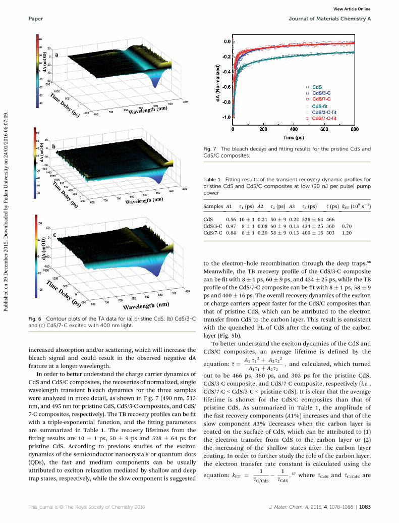
Fig. 6 Contour plots of the TA data for (a) pristine CdS; (b) CdS/3-Cand (c) CdS/7-C excited with 400 nm light.
Fig. 7 The bleach decays and fitting results for the pristine CdS andCdS/C composites.
Table 1 Fitting results of the transient recovery dynamic profiles forpristine CdS and CdS/C composites at low (90 nJ per pulse) pumppower
Samples A1 s1 (ps) A2 s2 (ps) A3 s3 (ps) �s (ps) kET (109 s�1)
CdS 0.56 10 � 1 0.21 50 � 9 0.22 528 � 64 466CdS/3-C 0.97 8 � 1 0.08 60 � 9 0.13 434 � 25 360 0.70CdS/7-C 0.84 8 � 1 0.20 58 � 9 0.13 400 � 16 303 1.20
Paper Journal of Materials Chemistry A
Publ
ishe
d on
09
Dec
embe
r 20
15. D
ownl
oade
d by
Fud
an U
nive
rsity
on
24/0
1/20
16 0
6:07
:09.
View Article Online
increased absorption and/or scattering, which will increase thebleach signal and could result in the observed negative dAfeature at a longer wavelength.
In order to better understand the charge carrier dynamics ofCdS and CdS/C composites, the recoveries of normalized, singlewavelength transient bleach dynamics for the three sampleswere analyzed in more detail, as shown in Fig. 7 (490 nm, 513nm, and 495 nm for pristine CdS, CdS/3-C composites, and CdS/7-C composites, respectively). The TB recovery proles can be twith a triple-exponential function, and the tting parametersare summarized in Table 1. The recovery lifetimes from thetting results are 10 � 1 ps, 50 � 9 ps and 528 � 64 ps forpristine CdS. According to previous studies of the excitondynamics of the semiconductor nanocrystals or quantum dots(QDs), the fast and medium components can be usuallyattributed to exciton relaxation mediated by shallow and deeptrap states, respectively, while the slow component is suggested
This journal is © The Royal Society of Chemistry 2016
to the electron–hole recombination through the deep traps.56
Meanwhile, the TB recovery prole of the CdS/3-C compositecan be t with 8� 1 ps, 60� 9 ps, and 434� 25 ps, while the TBprole of the CdS/7-C composite can be t with 8 � 1 ps, 58 � 9ps and 400� 16 ps. The overall recovery dynamics of the excitonor charge carriers appear faster for the CdS/C composites thanthat of pristine CdS, which can be attributed to the electrontransfer from CdS to the carbon layer. This result is consistentwith the quenched PL of CdS aer the coating of the carbonlayer (Fig. 5b).
To better understand the exciton dynamics of the CdS andCdS/C composites, an average lifetime is dened by the
equation: s ¼ A1 s12 þ A2s22
A1s1 þ A2s2; and calculated, which turned
out to be 466 ps, 360 ps, and 303 ps for the pristine CdS,CdS/3-C composite, and CdS/7-C composite, respectively (i.e.,CdS/7-C < CdS/3-C < pristine CdS). It is clear that the averagelifetime is shorter for the CdS/C composites than that ofpristine CdS. As summarized in Table 1, the amplitude ofthe fast recovery components (A1%) increases and that of theslow component A3% decreases when the carbon layer iscoated on the surface of CdS, which can be attributed to (1)the electron transfer from CdS to the carbon layer or (2)the increasing of the shallow states aer the carbon layercoating. In order to further study the role of the carbon layer,the electron transfer rate constant is calculated using the
equation: kET ¼ 1sC=CdS
� 1sCdS
; 57 where �sCdS and �sC/CdS are
J. Mater. Chem. A, 2016, 4, 1078–1086 | 1083
Journal of Materials Chemistry A Paper
Publ
ishe
d on
09
Dec
embe
r 20
15. D
ownl
oade
d by
Fud
an U
nive
rsity
on
24/0
1/20
16 0
6:07
:09.
View Article Online
the average lifetimes of CdS and CdS/C electrodes, respectively.The electron transfer rates for CdS/3-C and CdS/7-C are deter-mined to be 0.7 � 109 s�1 and 1.2 � 109 s�1, respectively. Theseresults suggest that the electron transfer from CdS to the carbonlayer occurs on an ultrafast time scale, which suggests stronginteraction between the carbon layer and CdS.
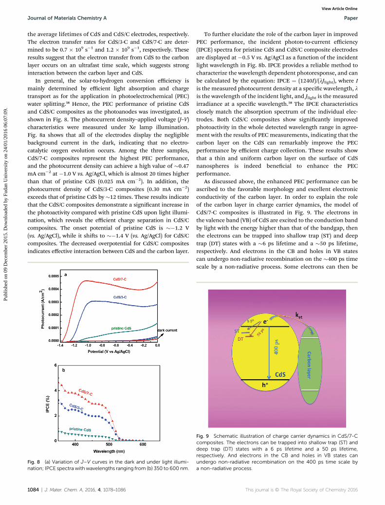
In general, the solar-to-hydrogen conversion efficiency ismainly determined by efficient light absorption and chargetransport as for the application in photoelectrochemical (PEC)water splitting.58 Hence, the PEC performance of pristine CdSand CdS/C composites as the photoanodes was investigated, asshown in Fig. 8. The photocurrent density–applied voltage (J–V)characteristics were measured under Xe lamp illumination.Fig. 8a shows that all of the electrodes display the negligiblebackground current in the dark, indicating that no electro-catalytic oxygen evolution occurs. Among the three samples,CdS/7-C composites represent the highest PEC performance,and the photocurrent density can achieve a high value of �0.47mA cm�2 at �1.0 V vs. Ag/AgCl, which is almost 20 times higherthan that of pristine CdS (0.025 mA cm�2). In addition, thephotocurrent density of CdS/3-C composites (0.30 mA cm�2)exceeds that of pristine CdS by �12 times. These results indicatethat the CdS/C composites demonstrate a signicant increase inthe photoactivity compared with pristine CdS upon light illumi-nation, which reveals the efficient charge separation in CdS/Ccomposites. The onset potential of pristine CdS is ��1.2 V(vs. Ag/AgCl), while it shis to ��1.4 V (vs. Ag/AgCl) for CdS/Ccomposites. The decreased overpotential for CdS/C compositesindicates effective interaction between CdS and the carbon layer.
Fig. 8 (a) Variation of J–V curves in the dark and under light illumi-nation; IPCE spectra with wavelengths ranging from (b) 350 to 600 nm.
1084 | J. Mater. Chem. A, 2016, 4, 1078–1086
To further elucidate the role of the carbon layer in improvedPEC performance, the incident photon-to-current efficiency(IPCE) spectra for pristine CdS and CdS/C composite electrodesare displayed at �0.5 V vs. Ag/AgCl as a function of the incidentlight wavelength in Fig. 8b. IPCE provides a reliable method tocharacterize the wavelength dependent photoresponse, and canbe calculated by the equation: IPCE ¼ (1240I)/(lJlight), where Iis the measured photocurrent density at a specic wavelength, lis the wavelength of the incident light, and Jlight is the measuredirradiance at a specic wavelength.58 The IPCE characteristicsclosely match the absorption spectrum of the individual elec-trodes. Both CdS/C composites show signicantly improvedphotoactivity in the whole detected wavelength range in agree-ment with the results of PEC measurements, indicating that thecarbon layer on the CdS can remarkably improve the PECperformance by efficient charge collection. These results showthat a thin and uniform carbon layer on the surface of CdSnanospheres is indeed benecial to enhance the PECperformance.
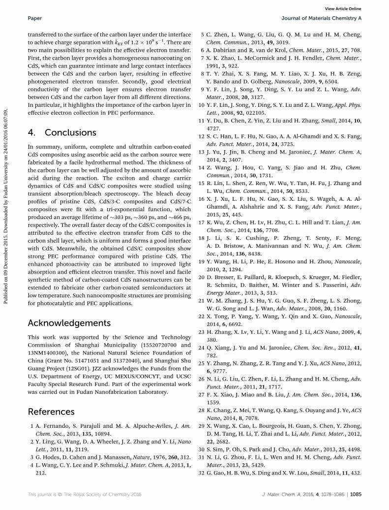
As discussed above, the enhanced PEC performance can beascribed to the favorable morphology and excellent electronicconductivity of the carbon layer. In order to explain the roleof the carbon layer in charge carrier dynamics, the model ofCdS/7-C composites is illustrated in Fig. 9. The electrons inthe valence band (VB) of CdS are excited to the conduction bandby light with the energy higher than that of the bandgap, thenthe electrons can be trapped into shallow trap (ST) and deeptrap (DT) states with a �6 ps lifetime and a �50 ps lifetime,respectively. And electrons in the CB and holes in VB statescan undergo non-radiative recombination on the �400 ps timescale by a non-radiative process. Some electrons can then be
Fig. 9 Schematic illustration of charge carrier dynamics in CdS/7-Ccomposites. The electrons can be trapped into shallow trap (ST) anddeep trap (DT) states with a 6 ps lifetime and a 50 ps lifetime,respectively. And electrons in the CB and holes in VB states canundergo non-radiative recombination on the 400 ps time scale bya non-radiative process.
This journal is © The Royal Society of Chemistry 2016
Paper Journal of Materials Chemistry A
Publ
ishe
d on
09
Dec
embe
r 20
15. D
ownl
oade
d by
Fud
an U
nive
rsity
on
24/0
1/20
16 0
6:07
:09.
View Article Online
transferred to the surface of the carbon layer under the interfaceto achieve charge separation with �kET of 1.2 � 109 s�1. There aretwo main possibilities to explain the effective electron transfer.First, the carbon layer provides a homogeneous nanocoating onCdS, which can guarantee intimate and large contact interfacesbetween the CdS and the carbon layer, resulting in effectivephotogenerated electron transfer. Secondly, good electricalconductivity of the carbon layer ensures electron transferbetween CdS and the carbon layer from all different directions.In particular, it highlights the importance of the carbon layer ineffective electron collection in PEC performance.
4. Conclusions
In summary, uniform, complete and ultrathin carbon-coatedCdS composites using ascorbic acid as the carbon source werefabricated by a facile hydrothermal method. The thickness ofthe carbon layer can be well adjusted by the amount of ascorbicacid during the reaction. The exciton and charge carrierdynamics of CdS and CdS/C composites were studied usingtransient absorption/bleach spectroscopy. The bleach decayproles of pristine CdS, CdS/3-C composites and CdS/7-Ccomposites were t with a tri-exponential function, whichproduced an average lifetime of�303 ps,�360 ps, and�466 ps,respectively. The overall faster decay of the CdS/C composites isattributed to the effective electron transfer from CdS to thecarbon shell layer, which is uniform and forms a good interfacewith CdS. Meanwhile, the obtained CdS/C composites showstrong PEC performance compared with pristine CdS. Theenhanced photoactivity can be attributed to improved lightabsorption and efficient electron transfer. This novel and facilesynthetic method of carbon-coated CdS nanostructures can beextended to fabricate other carbon-coated semiconductors atlow temperature. Such nanocomposite structures are promisingfor photocatalytic and PEC applications.
Acknowledgements
This work was supported by the Science and TechnologyCommission of Shanghai Municipality (15520720700 and13NM1400300), the National Natural Science Foundation ofChina (Grant No. 51471051 and 51372040), and Shanghai ShuGuang Project (12SG01). JZZ acknowledges the Funds from theU.S. Department of Energy, UC MEXUS/CONCYT, and UCSCFaculty Special Research Fund. Part of the experimental workwas carried out in Fudan Nanofabrication Laboratory.
References
1 A. Fernando, S. Parajuli and M. A. Alpuche-Aviles, J. Am.Chem. Soc., 2013, 135, 10894.
2 Y. Ling, G. Wang, D. A. Wheeler, J. Z. Zhang and Y. Li, NanoLett., 2011, 11, 2119.
3 G. Hodes, D. Cahen and J. Manassen, Nature, 1976, 260, 312.4 L. Wang, C. Y. Lee and P. Schmuki, J. Mater. Chem. A, 2013, 1,212.
This journal is © The Royal Society of Chemistry 2016
5 C. Zhen, L. Wang, G. Liu, G. Q. M. Lu and H. M. Cheng,Chem. Commun., 2013, 49, 3019.
6 A. Dabirian and R. van de Krol, Chem. Mater., 2015, 27, 708.7 X. K. Zhao, L. McCormick and J. H. Fendler, Chem. Mater.,1991, 3, 922.
8 T. Y. Zhai, X. S. Fang, M. Y. Liao, X. J. Xu, H. B. Zeng,Y. Bando and D. Golberg, Nanoscale, 2009, 9, 6504.
9 Y. F. Lin, J. Song, Y. Ding, S. Y. Lu and Z. L. Wang, Adv.Mater., 2008, 20, 3127.
10 Y. F. Lin, J. Song, Y. Ding, S. Y. Lu and Z. L. Wang, Appl. Phys.Lett., 2008, 92, 022105.
11 Y. Du, B. Chen, Z. Yin, Z. Liu and H. Zhang, Small, 2014, 10,4727.
12 S. C. Han, L. F. Hu, N. Gao, A. A. Al-Ghamdi and X. S. Fang,Adv. Funct. Mater., 2014, 24, 3725.
13 J. Yu, J. Jin, B. Cheng and M. Jaroniec, J. Mater. Chem. A,2014, 2, 3407.
14 Z. Wang, J. Hou, C. Yang, S. Jiao and H. Zhu, Chem.Commun., 2014, 50, 1731.
15 R. Lin, L. Shen, Z. Ren, W. Wu, Y. Tan, H. Fu, J. Zhang andL. Wu, Chem. Commun., 2014, 50, 8533.
16 X. J. Xu, L. F. Hu, N. Gao, S. X. Liu, S. Wageh, A. A. Al-Ghamdi, A. Alshahrie and X. S. Fang, Adv. Funct. Mater.,2015, 25, 445.
17 K. Wu, Z. Chen, H. Lv, H. Zhu, C. L. Hill and T. Lian, J. Am.Chem. Soc., 2014, 136, 7708.
18 J. Li, S. K. Cushing, P. Zheng, T. Senty, F. Meng,A. D. Bristow, A. Manivannan and N. Wu, J. Am. Chem.Soc., 2014, 136, 8438.
19 Y. Wang, H. Li, P. He, E. Hosono and H. Zhou, Nanoscale,2010, 2, 1294.
20 D. Bresser, E. Paillard, R. Kloepsch, S. Krueger, M. Fiedler,R. Schmitz, D. Baither, M. Winter and S. Passerini, Adv.Energy Mater., 2013, 3, 513.
21 W. M. Zhang, J. S. Hu, Y. G. Guo, S. F. Zheng, L. S. Zhong,W. G. Song and L. J. Wan, Adv. Mater., 2008, 20, 1160.
22 X. Tong, P. Yang, Y. Wang, Y. Qin and X. Guo, Nanoscale,2014, 6, 6692.
23 H. Zhang, X. Lv, Y. Li, Y. Wang and J. Li, ACS Nano, 2009, 4,380.
24 Q. Xiang, J. Yu and M. Jaroniec, Chem. Soc. Rev., 2012, 41,782.
25 Y. Zhang, N. Zhang, Z. R. Tang and Y. J. Xu, ACS Nano, 2012,6, 9777.
26 N. Li, G. Liu, C. Zhen, F. Li, L. Zhang and H. M. Cheng, Adv.Funct. Mater., 2011, 21, 1717.
27 F. X. Xiao, J. Miao and B. Liu, J. Am. Chem. Soc., 2014, 136,1559.
28 K. Chang, Z. Mei, T. Wang, Q. Kang, S. Ouyang and J. Ye, ACSNano, 2014, 8, 7078.
29 X. Wang, X. Cao, L. Bourgeois, H. Guan, S. Chen, Y. Zhong,D. M. Tang, H. Li, T. Zhai and L. Li, Adv. Funct. Mater., 2012,22, 2682.
30 S. Sim, P. Oh, S. Park and J. Cho, Adv. Mater., 2013, 25, 4498.31 N. Li, G. Zhou, F. Li, L. Wen and H. M. Cheng, Adv. Funct.
Mater., 2013, 23, 5429.32 G. Gao, H. B. Wu, S. Ding and X.W. Lou, Small, 2014, 11, 432.
J. Mater. Chem. A, 2016, 4, 1078–1086 | 1085
Journal of Materials Chemistry A Paper
Publ
ishe
d on
09
Dec
embe
r 20
15. D
ownl
oade
d by
Fud
an U
nive
rsity
on
24/0
1/20
16 0
6:07
:09.
View Article Online
33 Y. Hu, X. Gao, L. Yu, Y. Wang, J. Ning, S. Xu and X. W. Lou,Angew. Chem., 2013, 125, 5746.
34 J. Wang and X. Sun, Energy Environ. Sci., 2012, 5, 5163.35 H. Li and H. Zhou, Chem. Commun., 2012, 48, 1201.36 F. Wu, J. H. Yu, J. Joo, T. Hyeon and J. Z. Zhang, Opt. Mater.,
2007, 29, 858.37 T. Jia, A. Kolpin, C. Ma, R. C. T. Chan, W. M. Kwok and
S. E. Tsang, Chem. Commun., 2014, 50, 1185.38 J. Zhang, L. Qi, J. Ran, J. Yu and S. Z. Qiao, Adv. Energy Mater.,
2014, 4, 1301925.39 C. Han, Z. Chen, N. Zhang, J. C. Colmenares and Y. J. Xu,
Adv. Funct. Mater., 2015, 25, 170.40 S. Dutta, R. Sahoo, C. Ray, S. Sarkar, J. Jana, Y. Negishi and
T. Pal, Dalton Trans., 2015, 44, 193.41 L. V. Frolova, I. V. Magedov, A. Harper, S. K. Jha,
M. Ovezmyradov, G. Chandler, J. Garcia, D. Bethke,E. A. Shaner and I. Vasiliev, Carbon, 2015, 81, 216.
42 R. Beams, L. G. Cançado and L. Novotny, J. Phys.: Condens.Matter, 2015, 27, 083002.
43 J. Yang, J. Wang, Y. Tang, D. Wang, X. Li, Y. Hu, R. Li,G. Liang, T. K. Sham and X. Sun, Energy Environ. Sci., 2013,6, 1521.
44 X. Chen, W. Zhang, Q. Wang and J. Fan, Carbon, 2014, 79,165.
45 J. Bian, C. Huang, L. Wang, T. Hung, W. A. Daoud andR. Zhang, ACS Appl. Mater. Interfaces, 2014, 6, 4883.
1086 | J. Mater. Chem. A, 2016, 4, 1078–1086
46 L. Cao, X. Wang, M. J. Meziani, F. Lu, H. Wang, P. G. Luo,Y. Lin, B. A. Harruff, L. M. Veca and D. Murray, J. Am.Chem. Soc., 2007, 129, 11318.
47 R. Kostic and N. Romcevic, Phys. Status Solidi C, 2004, 1,2646.
48 G. Bertoni, V. Grillo, R. Brescia, X. Ke, S. Bals, A. Catellani,H. Li and L. Manna, ACS Nano, 2012, 6, 6453.
49 Z. X. Chi, W. Zhang, X. S. Wang, F. Q. Cheng, J. T. Chen,A. M. Cao and L. J. Wan, J. Mater. Chem. A, 2014, 2, 17359.
50 S. Yuvaraj, S. Amaresh, Y. Lee and R. K. Selvan, RSC Adv.,2014, 4, 6407.
51 Y. Zhang, Z. R. Tang, X. Fu and Y. J. Xu, ACS Nano, 2011, 5,7426.
52 S. Prezioso, F. Perrozzi, L. Giancaterini, C. Cantalini,E. Treossi, V. Palermo, M. Nardone, S. Santucci andL. Ottaviano, J. Phys. Chem. C, 2013, 117, 10683.
53 Z. B. Yu, Y. P. Xie, G. Liu, G. Q. M. Lu, X. L. Ma andH. M. Cheng, J. Mater. Chem. A, 2013, 1, 2773.
54 Y. Hu, H. Qian, Y. Liu, G. Du, F. Zhang, L. Wang and X. Hu,CrystEngComm, 2011, 13, 3438.
55 D. A. Wheeler and J. Z. Zhang, Adv. Mater., 2013, 25, 2878.56 J. K. Cooper, Y. Ling, C. Longo, Y. Li and J. Z. Zhang, J. Phys.
Chem. C, 2012, 116, 17360.57 Y. C. Pu, W. H. Lin and Y. J. Hsu, Appl. Catal., B, 2015, 163,
343.58 Q. Gui, Z. Xu, H. Zhang, C. Cheng, X. Zhu, M. Yin, Y. Song,
L. Lu, X. Chen and D. Li, ACS Appl. Mater. Interfaces, 2014,6, 17053.
This journal is © The Royal Society of Chemistry 2016