Embed Size (px)
Citation preview

452 | J. Mater. Chem. C, 2017, 5, 452--462 This journal is©The Royal Society of Chemistry 2017
Cite this: J.Mater. Chem. C, 2017,
5, 452
Measurement and modelling of dark currentdecay transients in perovskite solar cells†‡
Simon E. J. O’Kane,§a Giles Richardson,§b Adam Pockett,c Ralf G. Niemann,c
James M. Cave,*a Nobuya Sakai,d Giles E. Eperon,d Henry J. Snaith,d
Jamie M. Foster,e Petra J. Cameronc and Alison B. Walkera
The current decay in response to a sudden change of applied bias up to 1 V has been measured on a
methylammonium lead triiodide perovskite solar cell with titania and spiro-OMeTAD transport layers, for
temperatures between 258 and 308 K. These measurements are highly reproducible, in contrast to most
other techniques used to investigate perovskite cells. A drift–diffusion model that accounts for slow
moving ions as well as electrons and holes acting as charge carriers was used to predict the current
transients. The close fit of the model predictions to the measurements shows that mobile ions in the
perovskite layer influence transient behaviour on timescales of up to 50 s. An activation energy of 0.55 eV
is inferred from fitting simulations to measurements made at room temperature.
1 Introduction
Since their invention in 2009,1 organometal halide perovskitesolar cells have reached power conversion efficiencies (PCEs) ofover 20%. Recent reviews of perovskite solar cell technologies aregiven by Sum et al.,2 Stranks and Snaith,3 Niu et al.,4 Miyasaka5
and Park.6 Perovskites are the subject of a great deal of researchinterest due to their potential for easier and lower-cost manu-facture than the market-leading silicon-based technologies.
Historically, the credibility of reported PCE values for perov-skite solar cells has been undermined by widespread use of avoltage scanning protocol that takes advantage of hysteresis inthe current density–voltage ( J–V) characteristics of some cellsto obtain high initial PCE values that decrease as the cell is heldat the maximum power point (MPP) voltage. Zhang et al.7
measured how the efficiency fell over time for different cellarchitectures: in the most extreme case the PCE fell from 11.5%to zero. Hysteresis in the current–voltage characteristics ofperovskite solar cells was first reported in 20148 and confirmedby subsequent studies,9–12 although hysteresis loops in con-ductance measurements of bulk perovskite had been reportedearlier.13
In most perovskite solar cells, the organometal halide perov-skite absorber is sandwiched between an electron transporting(hole blocking) layer and a hole transporting (electron blocking)layer.14 One of the most commonly used,15 and indeed longestused,1 perovskites is methylammonium lead iodide (CH3NH3PbI3),or MAPI. The methylammonium (CH3NH3
+) cation has beensuccessfully replaced with formamidinium16 (NH2CHNH2
+) and/orcaesium17 (Cs+); a mixture of these cations can also be used.18,19
There are efforts to replace lead (Pb2+) with tin (Sn2+), though thisusually comes at the expense of performance and stability.20
Iodide can be replaced with other halides, either entirely or in amixture.3,21,22 The highest efficiency perovskite cells employmixed-cation lead mixed-halides.18,23–25
The hole transporting layer (HTL) usually consists of spiro-OMeTAD (2,20,7,70-tetrakis-(N,N-di-p-methoxyphenylamine)-9,90-spirobifluorene) that forms a planar heterojunction with theperovskite. The most commonly used electron transporting layer(ETL) is titania (TiO2), which can form either a mesostructured1
or planar26 heterojunction with the perovskite.Recently, there have been a number of well-documented
‘hysteresis-free’ cells27–31 in which the titania ETL is replacedwith a different material, popularly the fullerene derivativePCBM (phenyl-C61-butyric acid methyl ester). Often the spiroHTL is replaced as well, such as with the polymer PEDOT:PSS(poly(3,4-ethylenedioxythiophene)polystyrene sulfonate). It hasbeen argued that the removal of hysteresis by this change in theblocking materials demonstrates that ion motion in the perov-skite is not the source of hysteresis.27,32 However it is notablethat Bryant et al.33 demonstrate that apparently hysteresis-freecells employing PEDOT:PSS, MAPI and PCBM still exhibitsignificant hysteresis when cooled to 175 K and that hysteresis
a Department of Physics, University of Bath, UK. E-mail: [email protected] Mathematical Sciences, University of Southampton, UKc Department of Chemistry, University of Bath, UKd Department of Physics, University of Oxford, UKe Department of Mathematics, University of Portsmouth, UK
† The data used to produce Fig. 4–6 and 8 and ESI Fig. S1 are available atDOI: 10.15125/BATH-00251.‡ Electronic supplementary information (ESI) available. See DOI: 10.1039/c6tc04964h§ Authors contributed equally to this work.
Received 14th November 2016,Accepted 15th December 2016
DOI: 10.1039/c6tc04964h
www.rsc.org/MaterialsC
Journal ofMaterials Chemistry C
PAPER
Ope
n A
cces
s A
rtic
le. P
ublis
hed
on 1
5 D
ecem
ber
2016
. Dow
nloa
ded
on 1
5/02
/201
7 14
:03:
08.
Thi
s ar
ticle
is li
cens
ed u
nder
a C
reat
ive
Com
mon
s A
ttrib
utio
n 3.
0 U
npor
ted
Lic
ence
.
View Article OnlineView Journal | View Issue
This journal is©The Royal Society of Chemistry 2017 J. Mater. Chem. C, 2017, 5, 452--462 | 453
under normal operating conditions depends on the choice oftransport layer.34
In addition to hysteresis in both conductance and current–voltage measurements, unusual features have been observed inimpedance spectroscopy,8,35,36 intensity-modulated photocurrentspectroscopy (IMPS)35,36 and open-circuit voltage decay.36–38
These anomalies occur on the same timescale as the hysteresis,suggesting that they may have a common origin.
It was originally suspected13,39 that hysteresis was caused bythe creation of ferroelectric domains via dipoles in the methyl-ammonium (CH3NH3
+) ions, but this hypothesis has now beenruled out by electrical measurements.40 Two other possibleorigins of hysteresis have been proposed: large-scale trappingof electrons27,41,42 and mobile ions in the perovskite film.40,43,44
Yang et al.45 identified that iodide (I�) ions were moving, eithervia interstitials or vacancies. Walsh et al.46 calculated that theactivation energy required to form Schottky defects (vacancypairs) was much lower than that required to form Frenkel defects(an interstitial and a vacancy). Several computational studies47–50
have been conducted in order to calculate the activation energiesfor the migration of each ionic species in MAPI and otherperovskites; all agree that I� is the most mobile ion species,although the calculated values of activation energy for I� ionsvary between 0.08 eV and 0.58 eV.
While activation energies allow calculation of the rate at whichions move, the only way to evaluate the effect of ion motion oncurrent–voltage characteristics is with electrical transport model-ling. Similar to ions in an electrolyte, ionic charge accumulates inDebye layers (also termed double layers) at the edge of theperovskite under the influence of the built-in field.51 Li et al.52
used X-ray photoemission spectroscopy to measure the iodine tolead (I/Pb) ratio at various points in a MAPI film. They found thatapplication of an external field increased the I/Pb ratio at thepositive electrode, indicating a build-up of I� ions, and decreasedthe ratio at the negative electrode, indicating a depletion of I�
ions. Electron and hole densities are negligible in comparison toion vacancy densities at all applied voltages up to and includingthe built-in voltage. The result of this build-up of net charge isband bending, as postulated by Li et al.52 and others.12,47,51,53 Theband structure of the film as seen by charge carriers is modifiedelectrostatically by the Debye layers, which act to screen thebuilt-in field.
The Debye length is a measure of the characteristic width ofthese layers and is over two orders of magnitude smaller then theperovskite layer width (B1.5 nm compared to hundreds of nm)at the high ion vacancy densities encountered in perovskites.These narrow layers create a major computational challengewhen computing the solution over the entire width of theperovskite layer as a very fine mesh spacing is required torepresent the structure of the Debye layers. Richardson et al.51
argued that electron and hole densities are negligible incomparison to ion vacancy densities at all applied voltages upto and including the built-in voltage. They could then use themethod of matched asymptotic expansions to avoid this pitfalland model the Debye layers accurately, providing quantitativeagreement with experimental current–voltage curves in a model
assuming mobile ion vacancies and trap-assisted electron–holerecombination. Van Reenen et al.54 also found that both ionmotion and electron trapping were required to explain thecurrent–voltage hysteresis of the type observed in the literaturebut were unable to reproduce results in the physically relevantregime, nor to achieve quantitative comparison with experiment.We suggest a contributory factor is that the resolution of the finitedifference method employed by these authors was too coarse(4 nm) to accurately resolve the narrow Debye layers.
In this article we explore the effects of ion motion inperovskite solar cells by measuring their dark current decaytransients. These measurements are made in the dark bycausing the applied potential difference to jump from equili-brium, at 0 V, to Vjump and measuring the resulting current flowthrough the cell as a function of time. Prior to the measurementthe cell is held in the dark at open circuit for sufficient time toallow it to equilibrate (up to an hour at low temperatures). Nomore than 1 mV of residual voltage could remain after eachmeasurement for reproducibility on this level. This procedureensures reproducibility of the observed current trace by elimi-nating preconditioning effects; indeed we have shown thatrepeating the experiment on the same device by allowing it toequilibrate again after a measurement gives a result that exactlyoverlays the previous one. In contrast, most reported measuredcurrent–voltage characteristics suffer from irreproducibility –each time the measurement is made the results are different, evenfor the same device, as a result of residual preconditioning fromprevious measurements, slight changes in illumination etc.
Obtaining this repeatability allows us to eliminate extraneouseffects such as cell degradation and material changes arising fromexposure of the perovskite to light, the latter was discussed inGottesman et al.55 The measured current through a cell dependson the ability of charge carriers to traverse the energy landscape ofthe materials. As we later discuss in detail, ion motion has a signi-ficant effect on the electrostatic potential within the perovskitelayer. By probing the physics in this relatively simple setup, wegain crucial insight into the operation of perovskite cells duringstandard lab tests such as J–V curve sweeps and stabilised powerconversion efficiency measurements, and how, and to whatextent, ion motion may affect the results. We therefore improveour understanding of how perovskite-based cells behave undernormal generating conditions, and what material advantages maybe exploited and what barriers need to be overcome.
Here, we report measured dark current decay transients anduse the asymptotic method of Richardson et al.51 along with theexperimental results to perform a drift–diffusion simulation onthe system. We assume the diffusion coefficient D+(T) of iodideions shows Arrhenius behaviour as a function of temperature.47
By measuring and simulating the transients at a fixed tempera-ture for a range of Vjump, we deduce a value for the activationenergy for iodide ion movement for our cell. We then use theobtained D+(T) to simulate transients for a fixed Vjump at a varietyof temperatures and compare to experiment. Experiment andmodel employ a FTO:TiO2:MAPI:spiro-OMeTAD:Au cell, as shownin Fig. 1. The cell was fabricated using the chloride precursorroute as described in Section 2.4.
Paper Journal of Materials Chemistry C
Ope
n A
cces
s A
rtic
le. P
ublis
hed
on 1
5 D
ecem
ber
2016
. Dow
nloa
ded
on 1
5/02
/201
7 14
:03:
08.
Thi
s ar
ticle
is li
cens
ed u
nder
a C
reat
ive
Com
mon
s A
ttrib
utio
n 3.
0 U
npor
ted
Lic
ence
.View Article Online

454 | J. Mater. Chem. C, 2017, 5, 452--462 This journal is©The Royal Society of Chemistry 2017
By using the asymptotic model, most of the features observedin the experimental transients can be understood in terms ofion motion. The structure in our transient results (Fig. 5 and 8)provides the first direct evidence that the rate of charge injectioninto the device, i.e. the current, is dependent on the positionof mobile ions within the cell. This result is a corroborationof our earlier work suggesting ion motion is responsible forthe widely observed current–voltage hysteresis in perovskitedevices.51 Analysis of the effect of temperature variation on thetimescale of the transients confirms the thermally activatedmechanism of ion migration assumed by Eames et al.47 andothers.48–50
2 Methods2.1 Drift–diffusion model
The drift–diffusion model used in this work (see Richardsonet al.51 for details) couples electron and hole charge transport toiodide ion vacancy motion (other vacancies are assumed to beimmobile) within a perovskite layer and assumes that thecontacts with the blocking layers can be treated as metallicbecause of the high doping densities in these layers.
We implement this model in a two-step process. Firstly, theelectric potential f(x,t) – a function of position and time – isfound using a time-dependent asymptotic model that considerssolely the mobile I� vacancies and their effect on the potential,assuming that the contribution of electrons and holes to thepotential is negligible. A schematic diagram of the Debye layer atthe MAPI:spiro interface as modelled in this step is illustrated inFig. 2. We denote the position of the interface of the perovskitewith the titania as x = 0, and the interface of the perovskite withthe spiro as x = b. As the Debye layers are very thin compared tothe perovskite film width, we further denote the edge of theDebye layer on the titania side of the perovskite film as x = 0+ and
the edge of the layer on the spiro side as x = b�. The distinctionbetween b and b� is illustrated in Fig. 2. Secondly, a drift–diffusion calculation of electron and hole motion is performedusing this potential profile which can then be used to determinethe output current density J(t). An accurate calculation of thepotential f(x,t) and I� vacancy motion can be made by using anasymptotic method51 (based on earlier work57) that overcomesthe numerical difficulties encountered when tackling this stiffproblem and accounts for the vacancy charge build-up in thenarrow Debye layers (of size comparable to the Debye length Ld)in terms of a nonlinear capacitance.
The model and its asymptotic solution have previously beendescribed in detail51 and are briefly summarized here. Forvolume-averaged vacancy concentrations N0 4 1017 cm�3 itcan be assumed that the main contributions to space charge inthe perovskite are concentrated in the Debye layers adjacent tothe TiO2 and spiro blocking layers. The bulk of the perovskitebetween these two layers is therefore free of net charge.
Assuming that only the positively charged I� vacancies canmove and the negatively charged CH3NH3
+ and Pb2+ vacanciesare static, the charge per unit area Q in these layers is related to
Fig. 1 Band diagram of the device. Band edges for the perovskite andtransport layers are represented by solid lines, with energies relative to thevacuum level in eV labelled.56 Fermi levels for the contacts are depicted bydotted lines – values for these levels were not required by the model andare difficult to measure accurately, so are not given.
Fig. 2 Schematic of the band structure at the MAPI:spiro interface.Depletion of negative iodide ions (blue circles) from the region adjacentto the interface forms a positively-charged Debye layer. This results in apotential change Vþ across the layer.
Journal of Materials Chemistry C Paper
Ope
n A
cces
s A
rtic
le. P
ublis
hed
on 1
5 D
ecem
ber
2016
. Dow
nloa
ded
on 1
5/02
/201
7 14
:03:
08.
Thi
s ar
ticle
is li
cens
ed u
nder
a C
reat
ive
Com
mon
s A
ttrib
utio
n 3.
0 U
npor
ted
Lic
ence
.View Article Online

This journal is©The Royal Society of Chemistry 2017 J. Mater. Chem. C, 2017, 5, 452--462 | 455
the voltage drop V across them by the asymmetric capacitancerelation
QðVÞ ¼ epVT
LdsignðVÞ
ffiffiffiffiffiffiffiffiffiffiffiffiffiffiffiffiffiffiffiffiffiffiffiffiffiffiffiffiffiffiffiffiffiffiffiffiffiffiffiffiffiffiffiffiffiffiffiffiffiffi2 exp
VVT
� �� 1� V
VT
� �s; (1)
where ep is the permittivity of the perovskite and VT is thethermal voltage. We denote the surface charge density in theDebye layers adjacent to the spiro and TiO2 as Q+ and Q�respectively, and the magnitude of the potential drops acrossthese layers by Vþ and �V� respectively. Due to the large donorand acceptor densities in the TiO2 and spiro,6,58 leading to largeeffective relative permittivities, the potential drop across theseblocking layers is, to a good approximation, zero. The totalpotential drop across the perovskite layer is thus approximatelyequal to that across the entire cell, Vbi � V, where Vbi is thebuilt-in voltage and V the externally applied voltage. The totalpotential drop across the charge-neutral bulk perovskite region(between the Debye layers) is simply the total drop across theperovskite less the drops across the Debye layers. As the widthsof the Debye layers are small compared to the width of the entireperovskite layer (b = 450 nm), the electric field Ebulk across thebulk region is given by
Ebulk �Vbi � Vð Þ � Vþ þ V�
b: (2)
The potential is higher at the TiO2 interface than the spirointerface if the applied voltage V is less than the built-in voltageVbi, which without Debye layers results in a positive Ebulk. Apositive value of Ebulk results in electrons being driven towardsthe TiO2 and holes towards the spiro, which is desirable undernormal solar operating conditions. The Debye layers act to cancelEbulk, however, reducing charge extraction efficiency.
By considering charge conservation and the charge neutralityof the system, it can be shown51 that the problem of determiningthe electric field can be reduced to determining the solution ofthe single ordinary differential equation
dQþdt¼ qDþN0
VTEbulkðtÞ (3)
where Q+ is the areal charge density in the Debye layer nextto the spiro-OMeTAD hole-transporting layer, D+ the iodidevacancy diffusion coefficient, N0 the average iodide vacancydensity and VT the thermal voltage.
The difference between the model here and that reported inRichardson et al.51 is that here we model recombination by acombination of a bimolecular scheme within the perovskiteand so-called surface recombination between an electron in theTiO2 conduction band and a hole in the MAPI valence bandacross the interface. The bimolecular recombination rate Rb isgiven by
Rb(x,t) = B(np � ni2), (4)
where p(x,t) and n(x,t) are the hole and electron densities, ni theintrinsic carrier density and B the bimolecular recombinationcoefficient (a constant). The surface recombination rate betweenan electron in the titania and a hole at the edge of the Debyelayer on the titania side of the perovskite is given by
Rs(x = 0+,t) = vsp(x = 0+,t), (5)
where vs is the surface recombination velocity and p(x = 0+,t)is the hole density in the perovskite at the edge of the Debyelayer.
2.2 Choice of parameters
Table 1 shows the parameter definitions and values used in ourmodel. The (temperature dependent) electron density in theperovskite at the titania interface n(x = 0), hole density at thespiro interface p(x = b), intrinsic carrier density ni(T) and thermalvoltage VT(T) are given by
nðx ¼ 0Þ ¼ gc expEFt � EC
kBT
� �; (6)
pðx ¼ bÞ ¼ gv expEV � EFs
kBT
� �; (7)
niðTÞ ¼ffiffiffiffiffiffiffiffiffigcgv
pexp � Eg
2kBT
� �; (8)
Table 1 Parameters used in the drift–diffusion simulations. Reference numbers are given for those obtained from literature. The values given for thetemperature-dependent quantities Ld, n(x = 0), ni, p(x = b), and VT are for room temperature (298 K)
Symbol Description Value Source
b Perovskite layer width 450 nm MeasuredDN High T vacancy diffusion coefficient 1.35 � 10�3 cm2 s�1 Eames et al.47
EC Perovskite conduction band minimum �3.7 eV Schulz et al.56
EFs Spiro-OMeTAD Fermi level �5.0 eV Schulz et al.56
EFt TiO2 Fermi level �3.95 eV Schulz et al.56
Eg Perovskite bandgap 1.7 eV =EC � EV
EV Perovskite valence band maximum �5.4 eV Schulz et al.56
ep Static dielectric constant 24.1e0 Brivio et al.59
gc Conduction band density of states 8.1 � 1018 cm�3 Brivio et al.59
gv Valence band density of states 5.8 � 1018 cm�3 Brivio et al.59
Ld Debye length 1.5 nm =(epVT/(qN0))1/2
N0 I� volume-averaged vacancy density 1.6 � 1019 cm�3 Walsh et al.46
n(x = 0) Density of electrons in perovskite at TiO2 boundary 4.8 � 1014 cm�3 Eqn (6)ni Intrinsic carrier density 3.0 � 104 cm�3 Eqn (8)p(x = b) Density of holes in perovskite at spiro boundary 1.0 � 1012 cm�3 Eqn (7)VT Thermal voltage 0.0257 V Eqn (9)
Paper Journal of Materials Chemistry C
Ope
n A
cces
s A
rtic
le. P
ublis
hed
on 1
5 D
ecem
ber
2016
. Dow
nloa
ded
on 1
5/02
/201
7 14
:03:
08.
Thi
s ar
ticle
is li
cens
ed u
nder
a C
reat
ive
Com
mon
s A
ttrib
utio
n 3.
0 U
npor
ted
Lic
ence
.View Article Online

456 | J. Mater. Chem. C, 2017, 5, 452--462 This journal is©The Royal Society of Chemistry 2017
and
VT ¼kBT
q; (9)
where kB is the Boltzmann constant and T the absolute tempera-ture. Other symbols are defined in Table 1. According to Walshet al.46 the vacancy density N0 is also temperature-dependent,although N0 has been kept constant in this work due to the largeuncertainty on the variability of this quantity.
In practice, since the simplified asymptotic model is solved onlyin the charge-free bulk region between the thin Debye layers, werequire boundary conditions for the carrier densities at the edge ofthe Debye layers: n(x = 0+) for electrons and p(x = b�) for holes. Theseconditions are obtained by assuming that within the Debye layersboth electron and hole distributions are close to quasi-equilibriumand so are approximately Boltzmann distributed such that
nðxÞ � nðx ¼ 0Þ exp þfðxÞ � fð0ÞVT
� �very close to x ¼ 0;
(10)
pðxÞ � pðx ¼ bÞ exp �fðxÞ � fðbÞVT
� �very close to x ¼ b:
(11)
Given that there is a rapid jump in potential across the right-hand Debye layer of size f b�ð Þ � fðbÞ ¼ Vþ and across the left-hand Debye layer of size f 0þð Þ � fð0Þ ¼ V�, the appropriateboundary conditions on the simplified asymptotic model are
n x ¼ 0þð Þ ¼ nðx ¼ 0Þ exp V�VT
� �; (12)
p x ¼ b�ð Þ ¼ pðx ¼ bÞ exp �VþVT
� �: (13)
where n(x = 0) and p(x = b) are given by (6) and (7).Parameters found by fitting to dark current decay transient
measurements are shown in Table 2. The room-temperaturevalue of the I� vacancy diffusion coefficient D+ was tuned suchthat the time for the simulated dark current transient, as shownin Fig. 5, to reach a stable value matched the experiment. Theelectron and hole diffusion coefficients Dn = Dp were adjustedto achieve the best possible agreement regarding the currenttransient behaviour observed prior to stabilisation at T = 298 K,and were taken to be temperature independent. Savenije et al.60
find that the carrier diffusion coefficients are likely to vary as
T�0.6 – this changes the values of D+ and D� only very slightlyover our temperature range, and negligibly compared to otherparameters that vary exponentially with T. The need to fit D+, Dn
and Dp to our cell’s experimental data arises from sensitivity ofthe diffusion coefficients to grain morphology, which variesfrom cell to cell.
According to Eames et al.,47 the temperature dependence ofD+ is given by
DþðTÞ ¼ D1 exp � EA
kBT
� �; (14)
where EA is the activation energy for vacancy migration and DN
is a constant determined by the frequency at which the I� ionsattempt to move into a vacant site. Eames et al.47 assume anattempt frequency of 1012 Hz, resulting in the value of DN givenin Table 1. Using the fitted parameter for D+ at T = 298 K inTable 2, EA is found to be 0.55 eV, marginally lower than theEA = 0.58 eV found by Eames et al.47
2.3 Simulation protocol
The asymptotic model was used to simulate the equilibration of thecell at 0 V applied potential in the dark for a time teq before abruptlyjumping to Vjump, still in the dark, at t = 0. During equilibration theareal charge density accumulates to Q+ = �Q� = Qeq in the Debyelayer adjacent to the spiro. For T Z 298 K, teq = 30 s; for lowertemperatures teq(T) is inversely proportional to the vacancy diffu-sion coefficient D+(T), which is given by (14). The initial condition istaken to be no net charge in the Debye layers (Q+ = �Q� = 0) att =�teq, although the procedure is not dependent on this. A secondsimulation is then performed, with V = Vjump for t 4 0 and settingQ+ = Qeq at t = 0 as the initial condition. The second simulationyields the evolution of Q+ over time; this information can be used tofind the current density J(t) at any given point in time t.
2.4 Cell fabrication and measurements
For the experimental measurements, planar perovskite solarcells were made by spin coating of the mixed halide precursorsolution of CH3NH3I and PbCl2 (3 : 1 molar ratio) in DMF, witha toluene-drip quenching step to facilitate fast crystallization ofthe film. The full fabrication method is explained in detail inSakai et al.61 Compact TiO2 and spiro-OMeTAD were used asthe electron and hole transport layers respectively. The activearea of the cells was 0.19 cm2 as defined by the overlap of theFTO and gold contacts.
Current decay measurements were performed in the darkusing a Solartron Modulab XM electrochemical system. Care wastaken to ensure that all measurements were started from thesame equilibrium condition by leaving the cell in the dark atopen-circuit between measurements until the residual voltagedropped below 1 mV. This would take up to one hour at lowtemperatures. Temperature controlled measurements were per-formed using a Peltier element and DC temperature controller(Meerstetter Engineering).
We note that some MAPI cells fabricated using chlorideprecursors have been reported to contain residual chloride ions,and it is still an open question as to the effect of these ions
Table 2 Parameter values derived from fitting the drift–diffusion simula-tions to experiment. D+ is temperature-dependent; the value at roomtemperature (298 K) is given here
Symbol Description Value
B Bimolecular recombination factor 4.1 � 10�5 cm3 s�1
D+ I� vacancy diffusion coefficient 7.5 � 10�13 cm2 s�1
Dn Electron diffusion coefficient 0.21 cm2 s�1
Dp Hole diffusion coefficient 0.21 cm2 s�1
EA I� vacancy activation energy 0.55 eVVbi Built-in voltage 1.05 Vvs Surface recombination velocity 0.058 cm s�1
Journal of Materials Chemistry C Paper
Ope
n A
cces
s A
rtic
le. P
ublis
hed
on 1
5 D
ecem
ber
2016
. Dow
nloa
ded
on 1
5/02
/201
7 14
:03:
08.
Thi
s ar
ticle
is li
cens
ed u
nder
a C
reat
ive
Com
mon
s A
ttrib
utio
n 3.
0 U
npor
ted
Lic
ence
.View Article Online

This journal is©The Royal Society of Chemistry 2017 J. Mater. Chem. C, 2017, 5, 452--462 | 457
(if any) on cell behaviour. Sakai et al.16 discuss the crystalgrowth in films produced using PbCl2. XRD shows that initiallygrains of MAPbCl3 form readily over MAPI grains. During theannealing phase, the XRD peak corresponding to MAPbCl3
disappears as the peak for MAPI grows. They note that, duringcrystal growth, the MAPbCl3 acts as a template for MAPI phases.During annealing, I� ions replace Cl� ions, forming apparentlypure MAPI.
The source of controversy here is whether all of the chlorideions are actually removed from the film. In any case, there is aconsensus that iodide ions are present in far greater numbersthan chloride ions. Dar et al.62 used scanning transmissionelectron microscopy-energy dispersive spectroscopy (STEM-EDS)to find that films they produced using the chloride precursorroute were ‘chloride-free’. Yu et al.63 used energy dispersive X-rayspectrometry (EDX) and surface-sensitive X-ray photoelectronspectroscopy (XPS) and found what they called a ‘negligible’amount of Cl in a fully annealed film. However, Yu et al.63 donote a weak XPS signal corresponding to 1% Cl compared to I inthe top 20 nm of their film. In addition, chloride and iodide ionsattach to the same sites on the perovskite lattice. As halidemigration in perovskites is vacancy mediated, this means thatit is only necessary to account for one species of vacancy (seeFig. 3). Unless chloride ions are orders of magnitude more mobilethan iodides, the values of vacancy diffusion coefficient anddensity will be determined solely by the values for iodide ionsalone. Even in the case of extremely mobile chlorides the effecton the model is only to increase the effective vacancy mobility bya small amount. As MAPI cells that are not produced usingchloride precursors exhibit the same hysteresis as ours, we areconfident that it is iodide migration playing the major role in ourcell and any chloride contamination does not significantly impactthe results. We chose the chloride precursor method for thisstudy as cells produced in this manner have been found toexhibit better photovoltaic performance.61
3 Results
Measured device current–voltage characteristics under illumi-nation and the measurement statistics for the cell and batchfrom which it was chosen are given in the ESI.‡
3.1 Ion motion
The equilibrium conduction band profile across the perovskitelayer is depicted in the upper panels of Fig. 4. Since the Debyelayers in which the charge is located are narrow as describedabove, over 95% of the perovskite is free of net charge. Aroundequilibrium conditions the built-in voltage Vbi is fully screenedby charge build-up in the Debye layers (in the form of I�
vacancies), so that the electric field Ebulk in the net charge-freeperovskite bulk is zero. The mobile positively charged vacanciespile up against the interface with the spiro, resulting in most ofthe charge Q+ = Qeq on that side of the perovskite film beingconcentrated within a Debye length Ld of the spiro interface. Thenegative charges on the other hand cannot move, so the chargeQ� = �Qeq on the TiO2 side is formed by the region beingdepleted of positively charged vacancies. While the fraction ofiodide sites that are vacant in CH3NH3PbI3 is relatively large ataround 1 in 750 (0.4% of unit cells have a vacancy),46 there arestill far fewer sites vacant than there are occupied. This meansthere are only a small number of vacancies per unit volume thatcan be removed (filled) until there are none left, but many morevacancies can be piled up in the same volume. As a result, thecharge Q� on the TiO2 side accumulates over several Ld. Thegreater extent of the Debye layer adjacent to the TiO2 compared tothat adjacent to the spiro causes a greater magnitude of potentialdrop V�j j across the former compared to the potential drop Vþj jacross the latter.51 The value of Q+ after being held at 0 V for 30 s,denoted Qeq, was found to be 3.1 mC cm�2.
The evolution of the conduction band profile for the first 8 safter jumping from the equilibrium condition to Vjump = 1 V isdepicted in the lower panels of Fig. 4. When the voltage is firstswitched from 0 V to 1 V, Q+ is still equal to Qeq, causing Ebulk tobe large and negative; specifically, Ebulk = �Vjump/b at t = 0. Astime progresses, the positively charged iodide vacancies aredriven by the negative Ebulk to flow away from the spiro andback towards the TiO2, reducing Q+, |Q�| and |Ebulk|. After 8 s,|Ebulk| has decayed to less than 5% of its initial value. The decayis non-exponential.
While these results are specifically for TiO2:MAPI:spiro, wesuggest the principles found here transfer over to other trans-port layer configurations as we can see no mechanism wherebythe choice of transport layer could completely stop all ionmotion. Other materials would likely alter the size of the layersor shift the timescale of ionic behaviour. The stages in differentfabrication techniques for different layers and chemical effectsbetween the layers and perovskite during and after fabricationmay also play a role.
3.2 Dark current decay transients
Two dark current decay transient experiments were performed.In the first experiment, the absolute temperature T was fixed at298 K and different values of Vjump were used. Fig. 5 shows thesimulated (panel a) and measured (panel b) results of thisexperiment. The current density in this work is defined to bepositive when generation exceeds recombination (i.e. power isbeing generated) and negative when recombination exceeds
Fig. 3 Schematic of the arrangement of iodide ions (red), chloride ions(green) and vacancies in a generic lattice. The relative concentrations ofchloride ions and halide vacancies compared to iodide ions are exaggerated.
Paper Journal of Materials Chemistry C
Ope
n A
cces
s A
rtic
le. P
ublis
hed
on 1
5 D
ecem
ber
2016
. Dow
nloa
ded
on 1
5/02
/201
7 14
:03:
08.
Thi
s ar
ticle
is li
cens
ed u
nder
a C
reat
ive
Com
mon
s A
ttrib
utio
n 3.
0 U
npor
ted
Lic
ence
.View Article Online

458 | J. Mater. Chem. C, 2017, 5, 452--462 This journal is©The Royal Society of Chemistry 2017
generation (i.e. power is being consumed); it is thereforenegative in the dark.
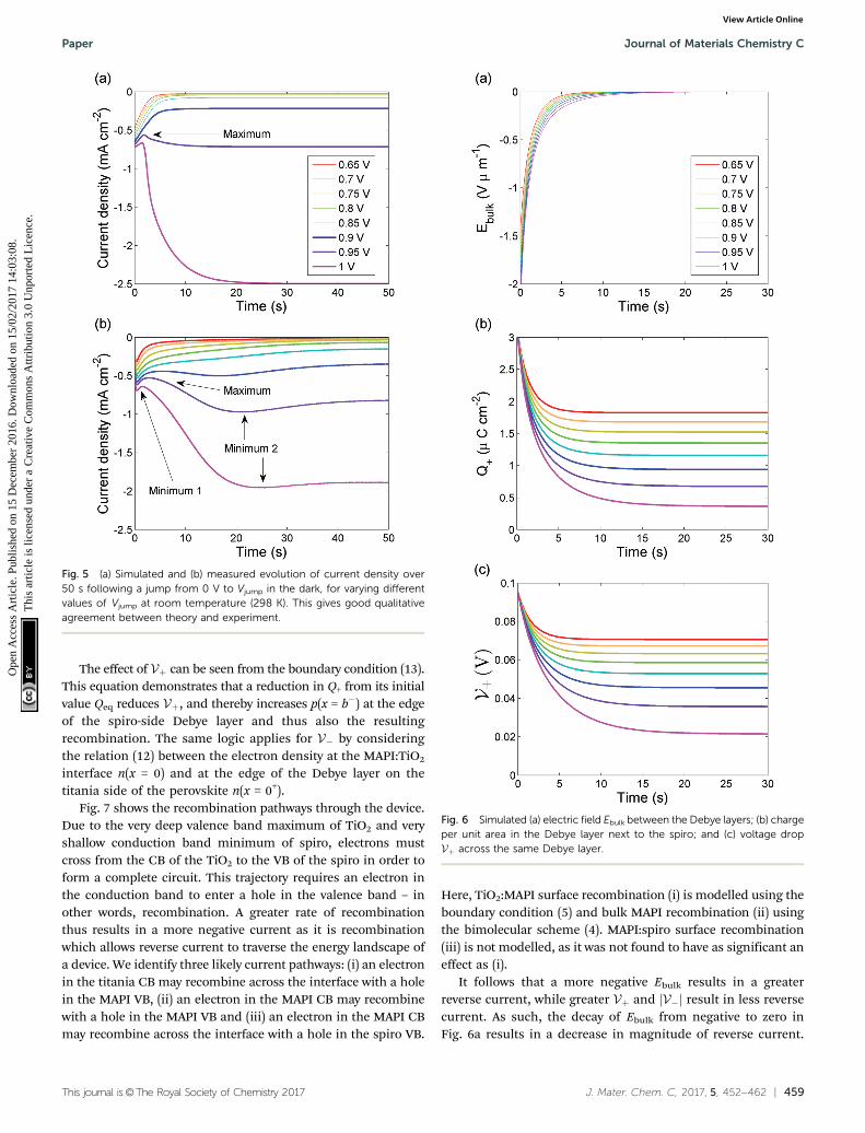
Assuming a diffusion coefficient D+ = 7.5 � 10�13 cm2 s�1 forthe I� vacancies, the agreement between simulation (Fig. 5a)and experiment (Fig. 5b) is good, both in terms of the magni-tudes of the current densities and the timescale of the decay.Crucially, the current density maximum observed at 3 s forVjump = 0.95 V in the measurement is predicted in the simula-tion – its origin is described below. However, the simulationsfail to predict the minima observed for all Vjump at around 1 s,labelled minimum 1 on Fig. 5b, as well as the minima seen ataround 20 s for Vjump Z 0.9 V, labelled minimum 2.
We believe the ‘spike’ at t = 0 in the experiment is due toelectron/hole displacement currents; these are beyond the scopeof this work and provide no insight into ion motion. Minimum 1occurs over short time scales on the order of 1 s and could haveits origins in competing recombination pathways or motion ofrelatively fast Li+ ions in the spiro hole transporting layer.Minimum 2 occurs at much longer timescales, on which theelectric field Ejump has been mostly compensated by the mobileions. Possible causes of this second minimum include the veryslow motion of methylammonium vacancies within the Debyelayers, the creation of additional vacancies at grain boundaries inthe perovskite film, or ions moving between the perovskite andelectron/hole transporting layers (as alluded to by Richardsonet al.51). Further development of the model will be necessary toexplain these discrepancies.
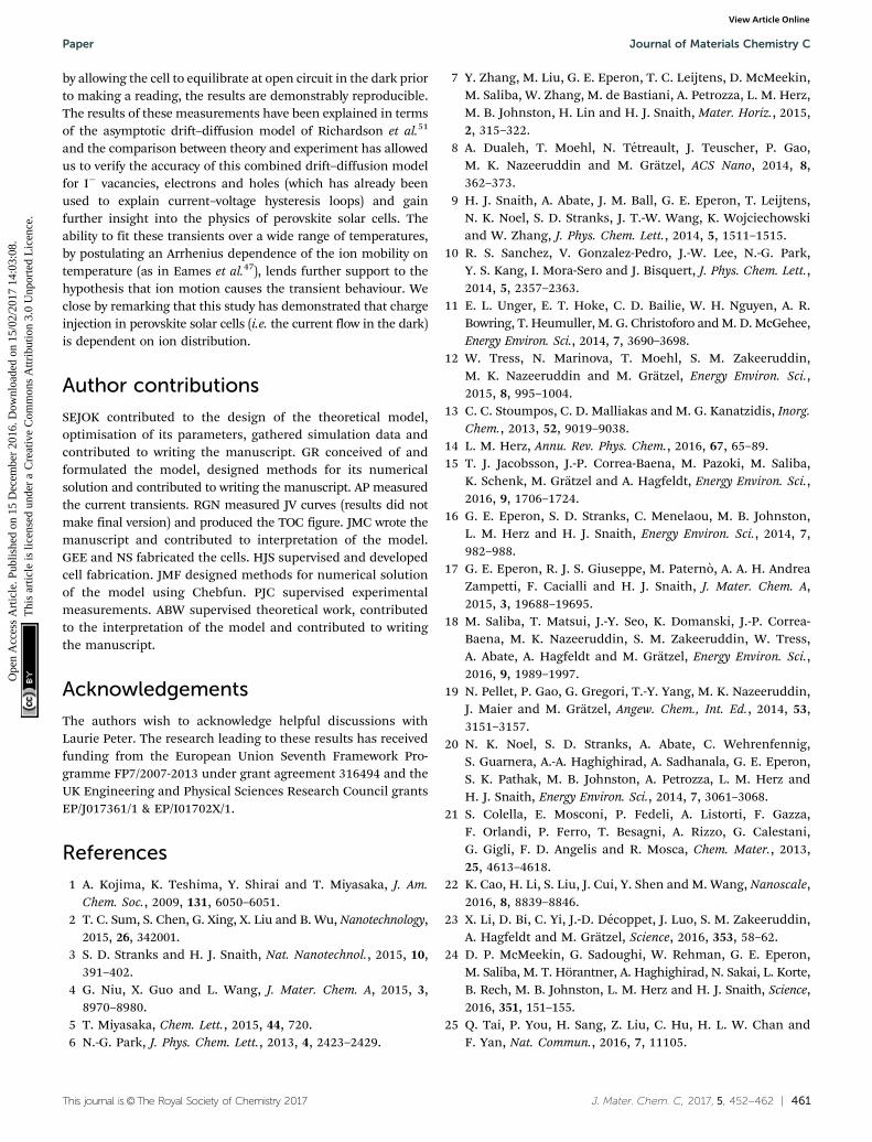
Fig. 6 shows the evolution of the bulk electric field Ebulk, theareal charge density Q+ in the Debye layer adjacent to the spiro
and the voltage drop Vþ across the same Debye layer. The bulkelectric field Ebulk is equal to �Vjump/b at t = 0 (when the jumpfrom 0 V to Vjump takes place) but returns to zero within 30 s.The Debye charge Q+ decays from Qeq to a smaller stable valueQs over the same timescale. This decay occurs because vacanciesmove out of the layer on the spiro side of the perovskite into thebulk and from the bulk into the layer on the side with titania dueto the reduced potential difference across the perovskite.
For values of Vjump less than the built-in voltage, 0 o Qs o Qeq,there is still a net potential difference across the device, though itis reduced to Vbi� Vjump. As there is a smaller potential difference,charge flows out of the Debye layers into the bulk, reducing Q+,|Q�| and the widths of the layers to the extent needed to screenthis smaller voltage. Lower values of Vjump thus correspond tolarger Qs, Vþ and V�j j, each in a nonlinear manner.
If Vjump equals Vbi exactly, Qs = 0. In this case there is nopotential difference across the perovskite, and so nothing tokeep the vacancies in the Debye layers. The Debye layers fullydischarge such that the vacancy density is uniform across theentirety of the perovskite.
As discussed by Richardson et al.51 the quantities that have amajor influence on recombination are Ebulk, Vþ and V�. NegativeEbulk hinders charge extraction as charges in the bulk are pushedto the opposite side of the perovskite bulk to their respectivetransport layers, causing carriers to build up. The increase incarrier density enhances recombination, as in (4) and (5). Afterthe initial jump in the applied potential Ebulk jumps to a negativevalue, causing a sudden increase in recombination, beforegradually relaxing to zero.
Fig. 4 Conduction band edge (CBE) across the 450 nm thick perovskite layer at 298 K, relative to the CBE immediately next to the titania. The centrepanels b and e show the entire perovskite layer. The left panels a and d show a close up of the Debye layer next to the titania; the right panels c and f showthe Debye layer next to the spiro. Upper panels: CB profile after the cell has been held at 0 V for 30 s, before the voltage jump. Lower panels: Evolutionover time of the CB profile for the first 8 s after switching the applied voltage from 0 V to Vjump = 1 V. The arrow indicates the direction of increasing time;the first line depicts the system immediately after the voltage jump at t = 0 s, with successive lines at 1 second intervals.
Journal of Materials Chemistry C Paper
Ope
n A
cces
s A
rtic
le. P
ublis
hed
on 1
5 D
ecem
ber
2016
. Dow
nloa
ded
on 1
5/02
/201
7 14
:03:
08.
Thi
s ar
ticle
is li
cens
ed u
nder
a C
reat
ive
Com
mon
s A
ttrib
utio
n 3.
0 U
npor
ted
Lic
ence
.View Article Online
This journal is©The Royal Society of Chemistry 2017 J. Mater. Chem. C, 2017, 5, 452--462 | 459
The effect of Vþ can be seen from the boundary condition (13).This equation demonstrates that a reduction in Q+ from its initialvalue Qeq reduces Vþ, and thereby increases p(x = b�) at the edgeof the spiro-side Debye layer and thus also the resultingrecombination. The same logic applies for V� by consideringthe relation (12) between the electron density at the MAPI:TiO2
interface n(x = 0) and at the edge of the Debye layer on thetitania side of the perovskite n(x = 0+).
Fig. 7 shows the recombination pathways through the device.Due to the very deep valence band maximum of TiO2 and veryshallow conduction band minimum of spiro, electrons mustcross from the CB of the TiO2 to the VB of the spiro in order toform a complete circuit. This trajectory requires an electron inthe conduction band to enter a hole in the valence band – inother words, recombination. A greater rate of recombinationthus results in a more negative current as it is recombinationwhich allows reverse current to traverse the energy landscape ofa device. We identify three likely current pathways: (i) an electronin the titania CB may recombine across the interface with a holein the MAPI VB, (ii) an electron in the MAPI CB may recombinewith a hole in the MAPI VB and (iii) an electron in the MAPI CBmay recombine across the interface with a hole in the spiro VB.
Here, TiO2:MAPI surface recombination (i) is modelled using theboundary condition (5) and bulk MAPI recombination (ii) usingthe bimolecular scheme (4). MAPI:spiro surface recombination(iii) is not modelled, as it was not found to have as significant aneffect as (i).
It follows that a more negative Ebulk results in a greaterreverse current, while greater Vþ and V�j j result in less reversecurrent. As such, the decay of Ebulk from negative to zero inFig. 6a results in a decrease in magnitude of reverse current.
Fig. 5 (a) Simulated and (b) measured evolution of current density over50 s following a jump from 0 V to Vjump in the dark, for varying differentvalues of Vjump at room temperature (298 K). This gives good qualitativeagreement between theory and experiment.
Fig. 6 Simulated (a) electric field Ebulk between the Debye layers; (b) chargeper unit area in the Debye layer next to the spiro; and (c) voltage dropVþ across the same Debye layer.
Paper Journal of Materials Chemistry C
Ope
n A
cces
s A
rtic
le. P
ublis
hed
on 1
5 D
ecem
ber
2016
. Dow
nloa
ded
on 1
5/02
/201
7 14
:03:
08.
Thi
s ar
ticle
is li
cens
ed u
nder
a C
reat
ive
Com
mon
s A
ttrib
utio
n 3.
0 U
npor
ted
Lic
ence
.View Article Online

460 | J. Mater. Chem. C, 2017, 5, 452--462 This journal is©The Royal Society of Chemistry 2017
At the same time, the decay of Vþ from B0.1 V to a smallervalue in Fig. 6c, and similar for V�, causes an increase inmagnitude of reverse current.
The balance between these two effects explains the behaviourof the current density transient J(t) in Fig. 5. For Vjump r 0.85 V theinfluence of Ebulk dominates causing J to increase then stabilise ata greater (less negative) value. For the case of Vjump Z 0.9 in theexperimental results, Ebulk dominates for a few seconds but thenthe V dominate after, causing J to increase to the maxima observedat t of a few seconds, then decrease again before settling to a stablevalue. The simulated results show these maxima for Vjump Z 0.95 V,but not Vjump = 0.9 V. Notably, the maximum for Vjump = 1 V occursat t = 1.5 s for both simulation and experiment.
3.3 Temperature dependence
A second dark current decay experiment was performed, whereVjump was set to 1 V and the temperature was varied. Tempera-ture variation was incorporated into the asymptotic model viaeqn (6)–(14). For absolute temperatures T o 298 K, holding thecell at 0 V for 30 s is not sufficient to reach equilibrium; thetime teq required to reach equilibrium is inversely proportionalto the vacancy diffusion coefficient D+(T). Six values of absolutetemperature T were investigated and the results shown in Fig. 8.
As with the results in Fig. 6, neither of the current densityminima observed in the measurements are present in thesimulation results, although the agreement is otherwise good.In particular, the simulated and measured current densitiesdecay on similar timescales for all the temperatures considered.If vacancy motion is a thermally activated mechanism (14),as proposed by Eames et al.,47 this temperature dependencesupports the hypothesis that the transients are a consequenceof ion motion.
The large reduction in the saturation current density reachedat large t as the temperature is reduced is also predicted by thesimulations. Notably saturation current density does not dependon ion motion; at long times the ion distribution reaches anequilibrium that is independent of temperature. Increases intemperature lead to increases in carrier concentrations on theperovskite boundaries (through (6) and (7)), hence to increasedcarrier concentrations throughout the perovskite layer andincreased recombination. In turn, this increased recombinationcauses negative saturation currents of greater magnitude at hightemperature (where carrier recombination is high) in comparisonto low temperature (where carrier recombination is low). The factthat the experimental and theoretical saturation current densitiesdo not match up is attributable to small errors in the Fermi levelsused to calculate the boundary conditions (6) and (7) on thecarrier concentration.
4 Conclusions
In conclusion, we have used dark current decay transient measure-ments to probe the physical behaviour of perovskite solar cells.This method has the significant advantage over other experimentalprocedures used to investigate charge transport in such cells that,
Fig. 7 Schematic of the possible paths reverse current can take throughthe device. The applied voltage V ‘pumps’ electrons (purple circles) fromthe gold electrode to the FTO. Upward-pointing green arrows representinjection barriers between materials the electrons must overcome toincrease in energy. Downward-pointing red arrows represent energeticallyfavourable recombination pathways. Electron transport in the MAPI andspiro valence bands is hole mediated.
Fig. 8 Simulated (panels a) and measured (panel b) evolution of currentdensity over 50 s following a jump from 0 V to 1 V in the dark, for sixdifferent values of absolute temperature T.
Journal of Materials Chemistry C Paper
Ope
n A
cces
s A
rtic
le. P
ublis
hed
on 1
5 D
ecem
ber
2016
. Dow
nloa
ded
on 1
5/02
/201
7 14
:03:
08.
Thi
s ar
ticle
is li
cens
ed u
nder
a C
reat
ive
Com
mon
s A
ttrib
utio
n 3.
0 U
npor
ted
Lic
ence
.View Article Online
This journal is©The Royal Society of Chemistry 2017 J. Mater. Chem. C, 2017, 5, 452--462 | 461
by allowing the cell to equilibrate at open circuit in the dark priorto making a reading, the results are demonstrably reproducible.The results of these measurements have been explained in termsof the asymptotic drift–diffusion model of Richardson et al.51
and the comparison between theory and experiment has allowedus to verify the accuracy of this combined drift–diffusion modelfor I� vacancies, electrons and holes (which has already beenused to explain current–voltage hysteresis loops) and gainfurther insight into the physics of perovskite solar cells. Theability to fit these transients over a wide range of temperatures,by postulating an Arrhenius dependence of the ion mobility ontemperature (as in Eames et al.47), lends further support to thehypothesis that ion motion causes the transient behaviour. Weclose by remarking that this study has demonstrated that chargeinjection in perovskite solar cells (i.e. the current flow in the dark)is dependent on ion distribution.
Author contributions
SEJOK contributed to the design of the theoretical model,optimisation of its parameters, gathered simulation data andcontributed to writing the manuscript. GR conceived of andformulated the model, designed methods for its numericalsolution and contributed to writing the manuscript. AP measuredthe current transients. RGN measured JV curves (results did notmake final version) and produced the TOC figure. JMC wrote themanuscript and contributed to interpretation of the model.GEE and NS fabricated the cells. HJS supervised and developedcell fabrication. JMF designed methods for numerical solutionof the model using Chebfun. PJC supervised experimentalmeasurements. ABW supervised theoretical work, contributedto the interpretation of the model and contributed to writingthe manuscript.
Acknowledgements
The authors wish to acknowledge helpful discussions withLaurie Peter. The research leading to these results has receivedfunding from the European Union Seventh Framework Pro-gramme FP7/2007-2013 under grant agreement 316494 and theUK Engineering and Physical Sciences Research Council grantsEP/J017361/1 & EP/I01702X/1.
References
1 A. Kojima, K. Teshima, Y. Shirai and T. Miyasaka, J. Am.Chem. Soc., 2009, 131, 6050–6051.
2 T. C. Sum, S. Chen, G. Xing, X. Liu and B. Wu, Nanotechnology,2015, 26, 342001.
3 S. D. Stranks and H. J. Snaith, Nat. Nanotechnol., 2015, 10,391–402.
4 G. Niu, X. Guo and L. Wang, J. Mater. Chem. A, 2015, 3,8970–8980.
5 T. Miyasaka, Chem. Lett., 2015, 44, 720.6 N.-G. Park, J. Phys. Chem. Lett., 2013, 4, 2423–2429.
7 Y. Zhang, M. Liu, G. E. Eperon, T. C. Leijtens, D. McMeekin,M. Saliba, W. Zhang, M. de Bastiani, A. Petrozza, L. M. Herz,M. B. Johnston, H. Lin and H. J. Snaith, Mater. Horiz., 2015,2, 315–322.
8 A. Dualeh, T. Moehl, N. Tetreault, J. Teuscher, P. Gao,M. K. Nazeeruddin and M. Gratzel, ACS Nano, 2014, 8,362–373.
9 H. J. Snaith, A. Abate, J. M. Ball, G. E. Eperon, T. Leijtens,N. K. Noel, S. D. Stranks, J. T.-W. Wang, K. Wojciechowskiand W. Zhang, J. Phys. Chem. Lett., 2014, 5, 1511–1515.
10 R. S. Sanchez, V. Gonzalez-Pedro, J.-W. Lee, N.-G. Park,Y. S. Kang, I. Mora-Sero and J. Bisquert, J. Phys. Chem. Lett.,2014, 5, 2357–2363.
11 E. L. Unger, E. T. Hoke, C. D. Bailie, W. H. Nguyen, A. R.Bowring, T. Heumuller, M. G. Christoforo and M. D. McGehee,Energy Environ. Sci., 2014, 7, 3690–3698.
12 W. Tress, N. Marinova, T. Moehl, S. M. Zakeeruddin,M. K. Nazeeruddin and M. Gratzel, Energy Environ. Sci.,2015, 8, 995–1004.
13 C. C. Stoumpos, C. D. Malliakas and M. G. Kanatzidis, Inorg.Chem., 2013, 52, 9019–9038.
14 L. M. Herz, Annu. Rev. Phys. Chem., 2016, 67, 65–89.15 T. J. Jacobsson, J.-P. Correa-Baena, M. Pazoki, M. Saliba,
K. Schenk, M. Gratzel and A. Hagfeldt, Energy Environ. Sci.,2016, 9, 1706–1724.
16 G. E. Eperon, S. D. Stranks, C. Menelaou, M. B. Johnston,L. M. Herz and H. J. Snaith, Energy Environ. Sci., 2014, 7,982–988.
17 G. E. Eperon, R. J. S. Giuseppe, M. Paterno, A. A. H. AndreaZampetti, F. Cacialli and H. J. Snaith, J. Mater. Chem. A,2015, 3, 19688–19695.
18 M. Saliba, T. Matsui, J.-Y. Seo, K. Domanski, J.-P. Correa-Baena, M. K. Nazeeruddin, S. M. Zakeeruddin, W. Tress,A. Abate, A. Hagfeldt and M. Gratzel, Energy Environ. Sci.,2016, 9, 1989–1997.
19 N. Pellet, P. Gao, G. Gregori, T.-Y. Yang, M. K. Nazeeruddin,J. Maier and M. Gratzel, Angew. Chem., Int. Ed., 2014, 53,3151–3157.
20 N. K. Noel, S. D. Stranks, A. Abate, C. Wehrenfennig,S. Guarnera, A.-A. Haghighirad, A. Sadhanala, G. E. Eperon,S. K. Pathak, M. B. Johnston, A. Petrozza, L. M. Herz andH. J. Snaith, Energy Environ. Sci., 2014, 7, 3061–3068.
21 S. Colella, E. Mosconi, P. Fedeli, A. Listorti, F. Gazza,F. Orlandi, P. Ferro, T. Besagni, A. Rizzo, G. Calestani,G. Gigli, F. D. Angelis and R. Mosca, Chem. Mater., 2013,25, 4613–4618.
22 K. Cao, H. Li, S. Liu, J. Cui, Y. Shen and M. Wang, Nanoscale,2016, 8, 8839–8846.
23 X. Li, D. Bi, C. Yi, J.-D. Decoppet, J. Luo, S. M. Zakeeruddin,A. Hagfeldt and M. Gratzel, Science, 2016, 353, 58–62.
24 D. P. McMeekin, G. Sadoughi, W. Rehman, G. E. Eperon,M. Saliba, M. T. Horantner, A. Haghighirad, N. Sakai, L. Korte,B. Rech, M. B. Johnston, L. M. Herz and H. J. Snaith, Science,2016, 351, 151–155.
25 Q. Tai, P. You, H. Sang, Z. Liu, C. Hu, H. L. W. Chan andF. Yan, Nat. Commun., 2016, 7, 11105.
Paper Journal of Materials Chemistry C
Ope
n A
cces
s A
rtic
le. P
ublis
hed
on 1
5 D
ecem
ber
2016
. Dow
nloa
ded
on 1
5/02
/201
7 14
:03:
08.
Thi
s ar
ticle
is li
cens
ed u
nder
a C
reat
ive
Com
mon
s A
ttrib
utio
n 3.
0 U
npor
ted
Lic
ence
.View Article Online

462 | J. Mater. Chem. C, 2017, 5, 452--462 This journal is©The Royal Society of Chemistry 2017
26 M. M. Lee, J. Teuscher, T. Miyasaka, T. N. Murakami andH. J. Snaith, Science, 2012, 338, 643–647.
27 Y. Shao, Z. Xiao, C. Bi, Y. Yuan and J. Huang, Nat. Commun.,2014, 5, 5784.
28 N. Tripathi, M. Yanagida, Y. Shirai, T. Masuda, L. Han andK. Miyano, J. Mater. Chem. A, 2015, 3, 12081.
29 Y. Hou, C. O. R. Quiroz, S. Scheiner, W. Chen, T. Stubhan,A. Hirsch, M. Halik and C. J. Brabec, Adv. Energy Mater.,2015, 5, 1501056.
30 H. Yoon, S. M. Kang, J.-K. Lee and M. Choi, Energy Environ.Sci., 2016, 9, 2262.
31 A. T. Mallajosyula, K. Fernando, S. Bhatt, A. Singh,B. W. Alphenaar, J.-C. Blancon, W. Nie, G. Gupta andA. D. Mohite, Mater. Today, 2016, 3, 96–102.
32 L. Cojocaru, S. Uchida, P. V. V. Jayaweera, S. Kaneko,J. Nakazaki, T. Kubo and H. Segawa, Chem. Lett., 2015, 44,1750–1752.
33 D. Bryant, S. Wheeler, B. C. O’Regan, T. Watson, P. R. F.Barnes, D. Worsley and J. Durrant, J. Phys. Chem. Lett., 2015,6, 3190–3194.
34 H.-S. Kim, I.-H. Jang, N. Ahn, M. Choi, A. Guerrero,J. Bisquert and N.-G. Park, J. Phys. Chem. Lett., 2015, 6,4633–4639.
35 E. Guillen, F. J. Ramos, J. A. Anta and S. Ahmad, J. Phys.Chem. C, 2014, 118, 22913–22922.
36 A. Pockett, G. E. Eperon, T. Peltola, H. J. Snaith, A. Walker,L. M. Peter and P. J. Cameron, J. Phys. Chem. C, 2015, 119,3456–3465.
37 A. Baumann, K. Tvingstedt, M. C. Heiber, S. Vath,C. Momblona, H. J. Bolink and V. Dyakonov, APL Mater.,2014, 2, 081501.
38 B. C. O’Regan, P. R. F. Barnes, X. Li, C. Law, E. Palomares andJ. M. Marin-Beloqui, J. Am. Chem. Soc., 2015, 137, 5087–5099.
39 J. M. Frost, K. T. Butler, F. Brivio, C. H. Hendon,M. van Schilfgaarde and A. Walsh, Nano Lett., 2014, 14,2584–2590.
40 J. Beilsten-Edmands, G. E. Eperon, R. D. Johnson, H. J. Snaithand P. G. Radaelli, Appl. Phys. Lett., 2015, 106, 173502.
41 H.-S. Duan, H. Zhou, Q. Chen, P. Sun, S. Luo, T.-B. Song,B. Bob and Y. Yang, Phys. Chem. Chem. Phys., 2015, 17,112–116.
42 J. H. Heo, D. H. Song, H. J. Han, S. Y. Kim, J. H. Kim, D. Kim,H. W. Shin, T. K. Ahn, C. Wolf, T.-W. Lee and S. H. Im, Adv.Mater., 2015, 27, 3424–3430.
43 O. Almora, I. Zarazua, I. Mas-Marza, E. Mora-Sero, J. Bisquertand G. Garcia-Belmonte, J. Phys. Chem. Lett., 2015, 6, 1645–1652.
44 J. Xu, A. Buin, A. H. Ip, W. Li, O. Voznyy, R. Comin, M. Yuan,S. Jeon, Z. Ning, J. J. McDowell, P. Kanjanaboos, J.-P. Sun,
X. Lan, L. N. Quan, D. H. Kim, I. G. Hill, P. Maksymovychand E. H. Sargent, Nat. Commun., 2015, 6, 7081.
45 T.-Y. Yang, G. Gregori, N. Pellet, M. Gratzel and J. Maier,Angew. Chem., Int. Ed., 2015, 54, 7905.
46 A. Walsh, D. O. Scanlon, S. Chen, X. G. Gong and S.-H. Wei,Angew. Chem., Int. Ed., 2015, 127, 1811.
47 C. Eames, J. M. Frost, P. R. F. Barnes, B. C. O’Regan,A. Walsh and M. S. Islam, Nat. Commun., 2015, 6, 7497.
48 J. M. Azpiroz, E. Mosconi, J. Bisquert and F. de Angelis,Energy Environ. Sci., 2015, 8, 2118–2127.
49 J. Haruyama, K. Sodeyama, L. Han and Y. Tateyama, J. Am.Chem. Soc., 2015, 137, 10048–10051.
50 S. Meloni, T. Moehl, W. Tress, M. Franckevicius, M. Saliba,Y. H. Lee, P. Gao, M. K. Nazeeruddin, S. M. Zakeeruddin,U. Rothlisberger and M. Gratzel, Nat. Commun., 2016,7, 10334.
51 G. Richardson, S. E. J. OKane, R. G. Niemann, T. A. Peltola,J. M. Foster, P. J. Cameron and A. B. Walker, Energy Environ.Sci., 2016, 9, 1476–1485.
52 C. Li, S. Tscheuschner, F. Paulus, P. E. Hopkinson,J. Kießling, A. Kohler, Y. Vaynzof and S. Huettner, Adv.Mater., 2016, 28, 2446–2454.
53 Y. Zhao, C. Liang, H. Zhang, D. Lu, D. Tian, G. Li, X. Jing,W. Zhang, W. Xiao, Q. Liu, F. Zhang and Z. He, EnergyEnviron. Sci., 2015, 8, 1256–1260.
54 S. van Reenen, M. Kemerink and H. J. Snaith, J. Phys.Chem. Lett., 2015, 6, 3808–3814.
55 R. Gottesman, L. Gouda, B. S. Kalanoor, E. Haltzi, S. Tirosh,E. Rosh-Hodesh, Y. Tischler, A. Zaban, C. Quarti andE. Mosconi, et al., J. Phys. Chem. Lett., 2015, 6, 2332–2338.
56 P. Schulz, E. Edri, S. Kirmayer, G. Hodes, D. Cahen andA. Kahn, Energy Environ. Sci., 2014, 7, 1377–1381.
57 G. Richardson, Math. Med. Biol., 2009, 26, 201–224.58 P. J. Cameron and L. M. Peter, J. Phys. Chem. B, 2003, 107,
14394–14400.59 F. Brivio, K. T. Butler, A. Walsh and M. van Schilfgaarde,
Phys. Rev. B: Condens. Matter Mater. Phys., 2014, 89, 155204.60 T. J. Savenije, C. S. Ponseca, L. Kunneman, M. Abdellah,
K. Zheng, Y. Tian, Q. Zhu, S. E. Canton, I. G. Scheblykin,T. Pullerits, A. Yartsev and V. Sundstrom, J. Phys. Chem.Lett., 2014, 5, 2189–2194.
61 N. Sakai, S. Pathak, H.-W. Chen, A. A. Haghighirad,S. D. Stranks, T. Miyasaka and H. J. Snaith, J. Mater.Chem. A, 2016, 4, 4464–4471.
62 M. I. Dar, N. Arora, P. Gao, S. Ahmad, M. Gratzel and M. K.Nazeeruddin, Nano Lett., 2014, 14, 6991–6996.
63 H. Yu, F. Wang, F. Xie, W. Li, J. Chen and N. Zhao,Adv. Funct. Mater., 2014, 24, 7102–7108.
Journal of Materials Chemistry C Paper
Ope
n A
cces
s A
rtic
le. P
ublis
hed
on 1
5 D
ecem
ber
2016
. Dow
nloa
ded
on 1
5/02
/201
7 14
:03:
08.
Thi
s ar
ticle
is li
cens
ed u
nder
a C
reat
ive
Com
mon
s A
ttrib
utio
n 3.
0 U
npor
ted
Lic
ence
.View Article Online