Embed Size (px)
Citation preview
Journal of Non-Crystalline Solids 355 (2009) 1508–1516
Contents lists available at ScienceDirect
Journal of Non-Crystalline Solids
journal homepage: www.elsevier .com/ locate / jnoncrysol
Amorphous to crystalline transition and optoelectronic propertiesof nanocrystalline indium tin oxide (ITO) films sputtered with highrf power at room temperature
V. Malathy a, S. Sivaranjani b, V.S. Vidhya c, J. Joseph Prince d, T. Balasubramanian a,C. Sanjeeviraja b, M. Jayachandran c,*
a Department of Physics, National Institute of Technology, Trichy-620 015, Indiab Department of Physics, Alagappa University, Karaikudi-630 003, Indiac ECMS Division, Central Electrochemical Research Institute, Karaikudi-630 006, Indiad Department of Physics, Anna University, Trichy-620 024, India
a r t i c l e i n f o a b s t r a c t
Article history:Received 11 December 2008Received in revised form 20 April 2009Available online 29 June 2009
PACS:81.07.Bc71.20.Nr81.15.Cd91.05.Cp78.66.W73.61.r
Keywords:UPS/XPSX-ray diffractionConductivitySputteringOptical spectroscopyAtomic force and scanning tunnelingmicroscopy
0022-3093/$ - see front matter � 2009 Published bydoi:10.1016/j.jnoncrysol.2009.04.043
* Corresponding author. Tel.: +91 04565 227555x2E-mail address: [email protected] (M. Jayachan
ITO thin films were deposited on quartz substrates by the rf sputtering technique using various rf powerkeeping the substrates at room temperature. The influence of rf power on the structural, electrical, opticaland morphological properties was studied by varying the rf power in the range 50–350 W. X-ray diffrac-tion results show an amorphous – crystalline transition with nano grains. At a power of 250 W, the ITOfilm showed preferential orientation along (4 0 0) peak. It is observed from the optical transmission stud-ies that the optical band gap increased from 3.57 to 3.69 eV when the rf power was increased from 50 to250 W. The resistivity value is minimum and grain size is maximum for the ITO film deposited at 250 W.The X-ray photoelectron spectroscopy (XPS), Energy dispersive X-ray (EDX) and Atomic force microscopyAFM results confirm that the ITO films are stoichiometric and the surface contained nano-sized grainsdistributed uniformly all over the surface. It can be concluded that the ITO film deposited at room tem-perature with 250 W rf power, can provide the required optical and electrical properties useful for devel-oping optoelectronic devices at lower temperatures.
� 2009 Published by Elsevier B.V.
1. Introduction
Thin films of transparent conducting oxide (TCO) have attractedgreater attention due to their interest optoelectronic properties ofhigh optical transparency in the visible wavelength region associ-ated with low sheet resistance [1]. This unique combination makesTCO films highly relevant to various applications and in developingoptoelectronic and electronic devices [2]. Among the many avail-able TCOs, ITO is the most frequently used material, both amor-phous and crystalline form, in developing practical optical andelectronic devices [3].
Indium tin oxides films have been deposited containing Sn4+
ions hosted in the In2O3 structure with concentrations varying up
Elsevier B.V.
18; fax: +91 04565 227713.dran).
to 15% [4]. ITO is a highly degenerate n-type semiconductor witha wide band gap (3.5–4.3 eV), having low enough electrical resistiv-ity of about 10�4 X cm making it easy to be interfaced with elec-tronic circuits and simultaneously shows high transmission in thevisible and near infrared (NIR) regions of the electromagnetic spec-trum [5]. Its low electrical resistivity results from either the non-stoichiometry produced by oxygen deficiency or by the incorpora-tion of tin as tetravalent dopant or from both [6]. Moreover, ITOexhibits excellent substrate adherence, hardness, and chemicalinertness. Because of these advantageous physico-chemical proper-ties ITO is widely used as transparent electrodes for optoelectronicdevices such as solar cells [7], flat panel displays [8], electro chro-mic devices [1], energy efficient windows, heat reflecting mirrorsand anti-reflection coatings [9] in addition to gas sensors [10].
The properties of ITO films such as electrical resistivity, opticaltransmittance, sensitivity to toxic gases are found to strongly
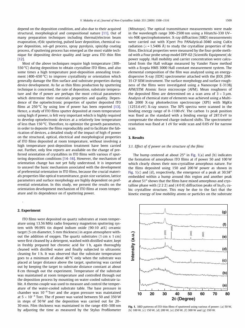
10 20 30 40 50 60 70 802θ (Degree)
(g)
(f)
(e)
(d)
(c)
(b)
(622
)
(440
)(400
)
Inte
nsi
ty (
a.u
.)
(222
)
(a)
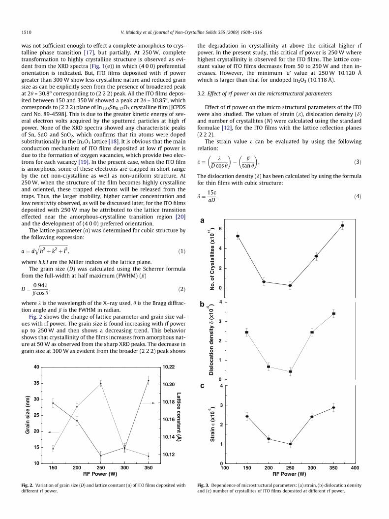
Fig. 1. XRD patterns of ITO thin films rf sputtered using various rf power: (a) 50 W,(b) 100 W, (c) 150 W, (d) 200 W, (e) 250 W, (f) 300 W and (g) 350 W.
V. Malathy et al. / Journal of Non-Crystalline Solids 355 (2009) 1508–1516 1509
depend on the deposition condition, and also due to their acquiredstructural, morphological and compositional nature [11]. Out ofmany preparation techniques including thermal/electron beamevaporation, rf/dc sputtering, pulsed laser deposition, chemical va-por deposition, sol–gel process, spray pyrolysis, spin/dip coatingprocess, rf sputtering process has emerged as the most viable tech-nique for depositing device quality and large area ITO thin film[12].
Most of the above techniques require high temperature (300–550 oC) during deposition to obtain crystalline ITO films, and alsosome times a high temperature post-deposition annealing treat-ment (400–650 oC) to improve crystallinity or orientation whichgenerally damage the film surface and substrate properties duringdevice development. As far as thin films production by sputteringtechnique is concerned, the rate of deposition, substrate tempera-ture and the rf power are perhaps the most critical parameterswhich determine their materials properties and quality. Depen-dence of the optoelectronic properties of sputter deposited ITOfilms at 250 oC by using low rf power has been reported [13].Hence, a study of ITO films sputter deposited at room temperatureusing high rf power, is felt very important which is highly requiredto develop optoelectronic devices at a relatively low temperatureof less than 150 oC. Therefore, to optimize the growth parameters,in order to deposite the films reproducibly and to facilitate the fab-rication of devices, a detailed study of the impact of high rf poweron the structural, optical, electrical and morphological propertiesof ITO films deposited at room temperature, without involving ahigh temperature post-deposition treatment have been carriedout. Further, only few reports are available on the change of pre-ferred orientation of crystallites in ITO films with various rf sput-tering deposition conditions [14–16]. However, the mechanism oforientation change has not yet fully understood. It is importantto unravel the basic mechanism associated with the developmentof preferential orientation in ITO films, because the crucial materi-als properties like optical transmittance, grain size variation, latticeparameters and surface morphology are highly dependent on pref-erential orientation. In this study, we present the results on theorientation development mechanism of ITO films at room temper-ature and its dependence on rf sputtering power.
.
2. Experiment
ITO films were deposited on quartz substrates at room temper-ature using 13.56 MHz radio frequency magnetron sputtering sys-tem with 99.99% tin doped indium oxide (90:10 at%) ceramictarget (5 cm diameter, 5 mm thickness) in argon atmosphere with-out the addition of oxygen. The quartz substrates (1 cm x 1 cm)were first cleaned by a detergent, washed with distilled water, keptin freshly prepared hot chromic acid for 1 h, again thoroughlycleaned with distilled water and finally subjected to ultrasoniccleaning for 1 h. It was observed that the substrate temperaturegoes to a minimum of about 40 oC only when the substrate wasplaced at larger distance above the target, sputtering was carriedout by keeping the target to substrate distance constant at about8 cm through out the experiment. Temperature of the substratewas maintained at room temperature and controlled through outthe deposition process by mounting on water-cooled substrate ta-ble. A thermo couple was used to measure and control the temper-ature of the water-cooled substrate table. The base pressure inchamber was 10�6 Torr and the argon pressure was maintainedat 5 � 10�3 Torr. The rf power was varied between 50 and 350 Win steps of 50 W and the deposition was carried out for 20–30 min. Film thickness was maintained in the range 450–500 nmby adjusting the time as measured by the Stylus Profilometer
(Mitutoyo). The optical transmittance measurements were madein the wavelength range 300–2500 nm using a Hitatchi-330 UV–vis-NIR spectrophotometer. X-ray diffraction (XRD) measurementswere carried out with X’pert Pro PANalytical-3040 using CuKaradiation (k = 1.5406 Å) to study the crystalline properties of thefilms. Electrical properties were measured by the four-probe meth-od with a Four probe setup model DFP-02 (Scientific Equipment) dcpower supply. Hall mobility and carrier concentration were calcu-lated from the Hall voltage measured by Vander Pauw methodwith a Ecopia HMS 3000 Hall constant measurement system. Theelemental composition of the film was analyzed using an energy-dispersive X-ray (EDX) spectrometer attached with the JEOL JSM-35 CF SEM instrument. The surface morphology and surface rough-ness of the films were investigated using a Nanoscope E-3138jAFM/STM Atomic force microscope (AFM). Mean roughness ofthe deposited films are determined on a scan area of 3 � 3 lm.Analysis of chemical state of elements was achieved using a Multi-lab 2000 X-ray photoelectron spectroscope (XPS) with MgKa(1253.6 eV) X-ray source. The XPS spectra were scanned in thebinding energy range of 0–1100 eV. The carbon 1s peak positionwas fixed as the standard with a binding energy of 287.0 eV tocompensate the observed charge-induced shifts. The spectrometerresolution was fixed at 1 eV for wide scan and 0.05 eV for narrowscan.
3. Results
3.1. Effect of rf power on the structure of the films
The hump centered at about 25o in Fig. 1(a) and (b) indicatesthe formation of amorphous ITO films at rf power 50 and 100 Wwhich clearly shows their non-crystalline amorphous nature. Forthe films deposited using 150 and 200 W power as shown inFig. 1(c) and (d), respectively, the emergence of a peak at 30.58o
embedded within a hump around this region and another peakat about 51o shows that the films have mixed amorphous and crys-talline phase with (2 2 2) and (4 0 0) diffraction peaks of In2O3 cu-bic crystalline structure. This may be due to the fact that thekinetic energy of low mobility atoms or particles on the substrate
0
2
4
6
No
. of
Cry
stal
lites
(x1
016)
2
3
4
tio
n d
ensi
ty δ
(x1
0-5)
a
b
1510 V. Malathy et al. / Journal of Non-Crystalline Solids 355 (2009) 1508–1516
was not sufficient enough to effect a complete amorphous to crys-talline phase transition [17], but partially. At 250 W, completetransformation to highly crystalline structure is observed as evi-dent from the XRD spectra (Fig. 1(e)) in which (4 0 0) preferentialorientation is indicated. But, ITO films deposited with rf powergreater than 300 W show less crystalline nature and reduced grainsize as can be explicitly seen from the presence of broadened peakat 2h = 30.8o corresponding to (2 2 2) peak. All the ITO films depos-ited between 150 and 350 W showed a peak at 2h = 30.85o, whichcorresponds to (2 2 2) plane of In1.88Sn0.12O3 crystalline film [JCPDScard No. 89-4598]. This is due to the greater kinetic energy of sev-eral electron volts acquired by the sputtered particles at high rfpower. None of the XRD spectra showed any characteristic peaksof Sn, SnO and SnO2, which confirms that tin atoms were dopedsubstitutionally in the In2O3 lattice [18]. It is obvious that the mainconduction mechanism of ITO films deposited at low rf power isdue to the formation of oxygen vacancies, which provide two elec-trons for each vacancy [19]. In the present case, when the ITO filmis amorphous, some of these electrons are trapped in short rangeby the net non-crystalline as well as non-uniform structure. At250 W, when the structure of the film becomes highly crystallineand oriented, these trapped electrons will be released from thetraps. Thus, the larger mobility, higher carrier concentration andlow resistivity observed, as will be discussed later, for the ITO filmsdeposited with 250 W may be attributed to the lattice transitioneffected near the amorphous-crystalline transition region [20]and the development of (4 0 0) preferred orientation.
The lattice parameter (a) was determined for cubic structure bythe following expression:
a ¼ dffiffiffiffiffiffiffiffiffiffiffiffiffiffiffiffiffiffiffiffiffiffiffiffiffih2 þ k2 þ l2
q; ð1Þ
where h,k,l are the Miller indices of the lattice plane.The grain size (D) was calculated using the Scherrer formula
from the full-width at half maximum (FWHM) (b)
D ¼ 0:94kb cos h
; ð2Þ
where k is the wavelength of the X–ray used, h is the Bragg diffrac-tion angle and b is the FWHM in radian.
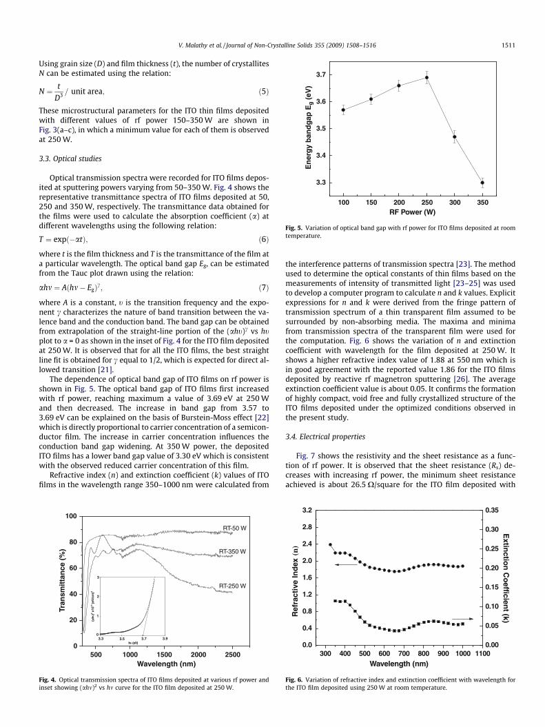
Fig. 2 shows the change of lattice parameter and grain size val-ues with rf power. The grain size is found increasing with rf powerup to 250 W and then shows a decreasing trend. This behaviorshows that crystallinity of the films increases from amorphous nat-ure at 50 W as observed from the sharp XRD peaks. The decrease ingrain size at 300 W as evident from the broader (2 2 2) peak shows
150 200 250 300 35010
15
20
25
30
35
40
RF Power (W)
Gra
in s
ize
(nm
)
10.12
10.14
10.16
10.18
10.20
10.22
Lattice co
nstan
t (Å)
Fig. 2. Variation of grain size (D) and lattice constant (a) of ITO films deposited withdifferent rf power.
the degradation in crystallinity at above the critical higher rfpower. In the present study, this critical rf power is 250 W wherehighest crystallinity is observed for the ITO films. The lattice con-stant value of ITO films decreases from 50 to 250 W and then in-creases. However, the minimum ‘a’ value at 250 W 10.120 Åwhich is larger than that for undoped In2O3 (10.118 Å).
3.2. Effect of rf power on the microstructural parameters
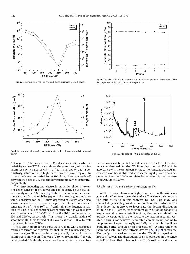
Effect of rf power on the micro structural parameters of the ITOwere also studied. The values of strain (e), dislocation density (d)and number of crystallites (N) were calculated using the standardformulae [12], for the ITO films with the lattice reflection planes(2 2 2).
The strain value e can be evaluated by using the followingrelation:
e ¼ kD cos h
� �� b
tan h
� �; ð3Þ
The dislocation density (d) has been calculated by using the formulafor thin films with cubic structure:
d ¼ 15eaD
; ð4Þ
100 150 200 250 300 350 4000
1
2
3
4
Str
ain
ε (
x10-3
)
RF Power (W)
0
1
Dis
loca
c
Fig. 3. Dependence of microstructural parameters: (a) strain, (b) dislocation densityand (c) number of crystallites of ITO films deposited at different rf power.
100 150 200 250 300 350
3.3
3.4
3.5
3.6
3.7
En
erg
y b
and
gap
Eg (
eV)
RF Power (W)
Fig. 5. Variation of optical band gap with rf power for ITO films deposited at roomtemperature.
V. Malathy et al. / Journal of Non-Crystalline Solids 355 (2009) 1508–1516 1511
Using grain size (D) and film thickness (t), the number of crystallitesN can be estimated using the relation:
N ¼ t
D3 = unit area; ð5Þ
These microstructural parameters for the ITO thin films depositedwith different values of rf power 150–350 W are shown inFig. 3(a–c), in which a minimum value for each of them is observedat 250 W.
3.3. Optical studies
Optical transmission spectra were recorded for ITO films depos-ited at sputtering powers varying from 50–350 W. Fig. 4 shows therepresentative transmittance spectra of ITO films deposited at 50,250 and 350 W, respectively. The transmittance data obtained forthe films were used to calculate the absorption coefficient (a) atdifferent wavelengths using the following relation:
T ¼ expð�atÞ; ð6Þ
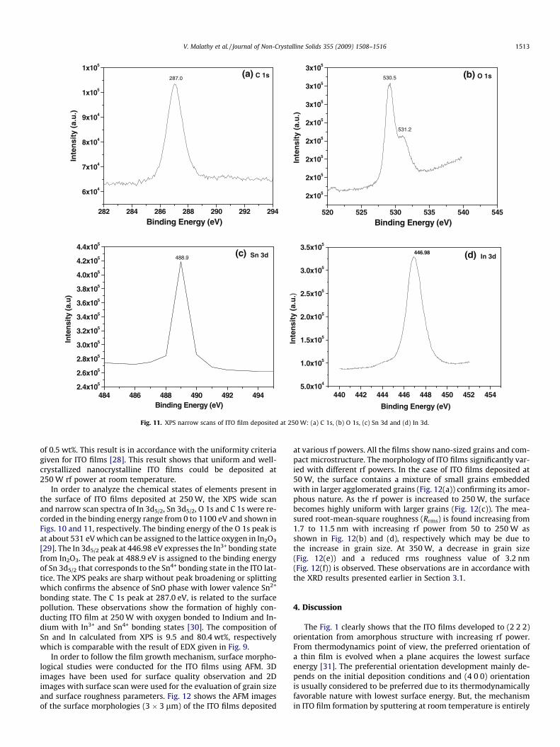
where t is the film thickness and T is the transmittance of the film ata particular wavelength. The optical band gap Eg, can be estimatedfrom the Tauc plot drawn using the relation:
ahm ¼ Aðhm� EgÞc; ð7Þ
where A is a constant, t is the transition frequency and the expo-nent c characterizes the nature of band transition between the va-lence band and the conduction band. The band gap can be obtainedfrom extrapolation of the straight-line portion of the (aht)c vs htplot to a = 0 as shown in the inset of Fig. 4 for the ITO film depositedat 250 W. It is observed that for all the ITO films, the best straightline fit is obtained for c equal to 1/2, which is expected for direct al-lowed transition [21].
The dependence of optical band gap of ITO films on rf power isshown in Fig. 5. The optical band gap of ITO films first increasedwith rf power, reaching maximum a value of 3.69 eV at 250 Wand then decreased. The increase in band gap from 3.57 to3.69 eV can be explained on the basis of Burstein-Moss effect [22]which is directly proportional to carrier concentration of a semicon-ductor film. The increase in carrier concentration influences theconduction band gap widening. At 350 W power, the depositedITO films has a lower band gap value of 3.30 eV which is consistentwith the observed reduced carrier concentration of this film.
Refractive index (n) and extinction coefficient (k) values of ITOfilms in the wavelength range 350–1000 nm were calculated from
500 1000 1500 2000 25000
20
40
60
80
100
RT-250 W
Tran
smit
tan
ce (
%)
Wavelength (nm)
RT-50 W
RT-350 W
3
2
1
03.93.73.53.3
hν (eV)
(αhν
)2 x10
13 (
eV/c
m)2
Fig. 4. Optical transmission spectra of ITO films deposited at various rf power andinset showing (ahm)2 vs hm curve for the ITO film deposited at 250 W.
the interference patterns of transmission spectra [23]. The methodused to determine the optical constants of thin films based on themeasurements of intensity of transmitted light [23–25] was usedto develop a computer program to calculate n and k values. Explicitexpressions for n and k were derived from the fringe pattern oftransmission spectrum of a thin transparent film assumed to besurrounded by non-absorbing media. The maxima and minimafrom transmission spectra of the transparent film were used forthe computation. Fig. 6 shows the variation of n and extinctioncoefficient with wavelength for the film deposited at 250 W. Itshows a higher refractive index value of 1.88 at 550 nm which isin good agreement with the reported value 1.86 for the ITO filmsdeposited by reactive rf magnetron sputtering [26]. The averageextinction coefficient value is about 0.05. It confirms the formationof highly compact, void free and fully crystallized structure of theITO films deposited under the optimized conditions observed inthe present study.
3.4. Electrical properties
Fig. 7 shows the resistivity and the sheet resistance as a func-tion of rf power. It is observed that the sheet resistance (Rs) de-creases with increasing rf power, the minimum sheet resistanceachieved is about 26.5 X/square for the ITO film deposited with
300 400 500 600 700 800 900 1000 11000.0
0.4
0.8
1.2
1.6
2.0
2.4
2.8
3.2
Wavelength (nm)
Ref
ract
ive
Ind
ex
0.00
0.05
0.10
0.15
0.20
0.25
0.30
0.35
Extin
ction
Co
efficient (k)
(n)
Fig. 6. Variation of refractive index and extinction coefficient with wavelength forthe ITO film deposited using 250 W at room temperature.
50 100 150 200 250 300 35010-3
10-2
10-1
100
101
102
103
ρ R
s
RF Power (W)
Res
isti
vity
ρ (
Ωcm
)
Sh
eet Resistan
ce Rs
(Ω/sq
uare )101
102
103
104
105
106
107
Fig. 7. Dependence of resistivity q and sheet resistance Rs on rf power.
100 150 200 250 300 350
1018
1019
1020
1021
RF Power (W)
Car
rier
Co
nce
ntr
atio
n (
cm-3)
0
2
4
6
8
Mo
bility (cm
2/Vs)
Fig. 8. Carrier concentration (n) and mobility (l) of ITO films deposited at various rfpower.
Sn % In %
1 2 3 4 5 60
10
20
30
40
50
60
70
80
90
100
Points
Ele
men
tal C
om
po
siti
on
(w
t%)
Fig. 9. Variation of In and Sn concentration at different points on the surface of ITOfilm deposited with 250 W at room temperature.
Fig. 10. XPS scan of ITO film deposited at 250 W.
1512 V. Malathy et al. / Journal of Non-Crystalline Solids 355 (2009) 1508–1516
250 W power. Then an increase in Rs values is seen. Similarly, theresistivity value of ITO film also shows the same trend, with a min-imum resistivity value of 4.3 � 10�3 X cm at 250 W and largerresistivity values on both higher and lower rf power regions. Inorder to achieve low resistivity in ITO films, there is a trade offbetween their resistivity and the corresponding carrier concentra-tion/mobility.
The semiconducting and electronic properties show an excel-lent dependence on the rf power and consequently on the crystal-line quality of the ITO films. Fig. 8 shows the variation of carrierconcentration (n) and mobility (l) with rf power. Highest mobilityvalue is observed for the ITO films deposited at 250 W which alsoshows the lowest resistivity with the presence of maximum carrierconcentration of 1.75 � 1020 cm�3 confirming the degenerate nat-ure of this ITO film. The recorded carrier concentration values showa variation of about 1018–1020 cm�3 for the ITO films deposited at100 and 250 W, respectively. This shows the transformation ofamorphous ITO films formed at rf power less than 100 W to wellcrystallized films at 250 W.
These electrical properties show that ITO films with amorphousnature are formed for rf power less that 100 W. On increasing thepower, the crystalline nature increases gradually and attains max-imum crystallinity at an rf power of 250 W. Beyond this rf power,the deposited ITO film shows a reduced value of carrier concentra-
tion exposing a deteriorated crystalline nature. The lowest resistiv-ity value observed for the ITO films deposited at 250 W is inaccordance with the trend seen for the carrier concentration. An in-crease in mobility is observed with increasing rf power which be-came maximum at 250 W and then decreased on further increaseof power, up to 350 W.
3.5. Microstructure and surface morphology studies
All the deposited films were highly transparent in the visible re-gion and uniform over the entire surface. The elemental composi-tion ratio of Sn to In was analyzed by EDX. This study wasconducted by selecting six different points on the surface of ITOfilms deposited at 250 W to investigate the dopant distributionof Sn in the ITO lattice. Since uniform distribution of dopants isvery essential in nanocrystalline films, the dopants should beexactly incorporated into the matrix to the maximum extent pos-sible. If this is not achieved, segregated doping occurs leading tothe presence of separated In2O3 and SnO2 particles which will de-grade the optical and electrical properties of ITO films renderingthem not useful in optoelectronic devices [27]. Fig. 9 shows theEDX analysis at various points on the ITO films deposited at250 W rf power. The distribution of Sn is observed in the rangeof 8–11 wt% and that of In about 79–82 wt% with in the deviation
440 442 444 446 448 450 452 4545.0x104
1.0x10⁵
1.5x10⁵
2.0x10⁵
2.5x10⁵
3.0x10⁵
3.5x10⁵
Inte
nsi
ty (
a.u
.)
Binding Energy (eV)
In 3d446.98 (d)
520 525 530 535 540 545
2x10⁵
2x10⁵
2x10⁵
2x10⁵
2x10⁵
3x10⁵
3x10⁵
3x10⁵
O 1s
531.2
Inte
nsi
ty (
a.u
.)
Binding Energy (eV)
530.5 (b)
282 284 286 288 290 292 294
6x10⁴
7x10⁴
8x10⁴
9x10⁴
1x10⁵
1x10⁵
Inte
nsi
ty (
a.u
.)
Binding Energy (eV)
287.0 C 1s(a)
484 486 488 490 492 4942.4x105
2.6x10⁵
2.8x10⁵
3.0x10⁵
3.2x10⁵
3.4x10⁵
3.6x10⁵
3.8x10⁵
4.0x10⁵
4.2x10⁵
4.4x10⁵
Sn 3d
Inte
nsi
ty (
a.u
)
Binding Energy (eV)
488.9(c)
Fig. 11. XPS narrow scans of ITO film deposited at 250 W: (a) C 1s, (b) O 1s, (c) Sn 3d and (d) In 3d.
V. Malathy et al. / Journal of Non-Crystalline Solids 355 (2009) 1508–1516 1513
of 0.5 wt%. This result is in accordance with the uniformity criteriagiven for ITO films [28]. This result shows that uniform and well-crystallized nanocrystalline ITO films could be deposited at250 W rf power at room temperature.
In order to analyze the chemical states of elements present inthe surface of ITO films deposited at 250 W, the XPS wide scanand narrow scan spectra of In 3d5/2, Sn 3d5/2, O 1s and C 1s were re-corded in the binding energy range from 0 to 1100 eV and shown inFigs. 10 and 11, respectively. The binding energy of the O 1s peak isat about 531 eV which can be assigned to the lattice oxygen in In2O3
[29]. The In 3d5/2 peak at 446.98 eV expresses the In3+ bonding statefrom In2O3. The peak at 488.9 eV is assigned to the binding energyof Sn 3d5/2 that corresponds to the Sn4+ bonding state in the ITO lat-tice. The XPS peaks are sharp without peak broadening or splittingwhich confirms the absence of SnO phase with lower valence Sn2+
bonding state. The C 1s peak at 287.0 eV, is related to the surfacepollution. These observations show the formation of highly con-ducting ITO film at 250 W with oxygen bonded to Indium and In-dium with In3+ and Sn4+ bonding states [30]. The composition ofSn and In calculated from XPS is 9.5 and 80.4 wt%, respectivelywhich is comparable with the result of EDX given in Fig. 9.
In order to follow the film growth mechanism, surface morpho-logical studies were conducted for the ITO films using AFM. 3Dimages have been used for surface quality observation and 2Dimages with surface scan were used for the evaluation of grain sizeand surface roughness parameters. Fig. 12 shows the AFM imagesof the surface morphologies (3 � 3 lm) of the ITO films deposited
at various rf powers. All the films show nano-sized grains and com-pact microstructure. The morphology of ITO films significantly var-ied with different rf powers. In the case of ITO films deposited at50 W, the surface contains a mixture of small grains embeddedwith in larger agglomerated grains (Fig. 12(a)) confirming its amor-phous nature. As the rf power is increased to 250 W, the surfacebecomes highly uniform with larger grains (Fig. 12(c)). The mea-sured root-mean-square roughness (Rrms) is found increasing from1.7 to 11.5 nm with increasing rf power from 50 to 250 W asshown in Fig. 12(b) and (d), respectively which may be due tothe increase in grain size. At 350 W, a decrease in grain size(Fig. 12(e)) and a reduced rms roughness value of 3.2 nm(Fig. 12(f)) is observed. These observations are in accordance withthe XRD results presented earlier in Section 3.1.
4. Discussion
The Fig. 1 clearly shows that the ITO films developed to (2 2 2)orientation from amorphous structure with increasing rf power.From thermodynamics point of view, the preferred orientation ofa thin film is evolved when a plane acquires the lowest surfaceenergy [31]. The preferential orientation development mainly de-pends on the initial deposition conditions and (4 0 0) orientationis usually considered to be preferred due to its thermodynamicallyfavorable nature with lowest surface energy. But, the mechanismin ITO film formation by sputtering at room temperature is entirely
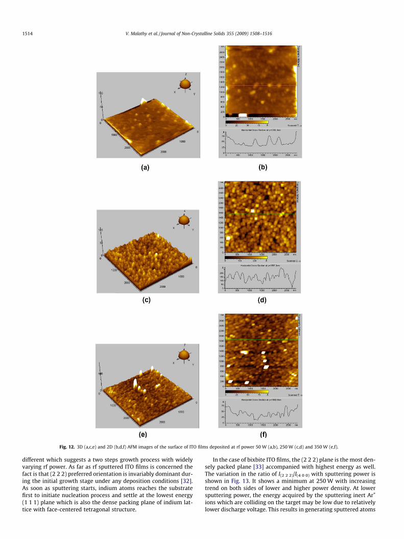
Fig. 12. 3D (a,c,e) and 2D (b,d,f) AFM images of the surface of ITO films deposited at rf power 50 W (a,b), 250 W (c,d) and 350 W (e,f).
1514 V. Malathy et al. / Journal of Non-Crystalline Solids 355 (2009) 1508–1516
different which suggests a two steps growth process with widelyvarying rf power. As far as rf sputtered ITO films is concerned thefact is that (2 2 2) preferred orientation is invariably dominant dur-ing the initial growth stage under any deposition conditions [32].As soon as sputtering starts, indium atoms reaches the substratefirst to initiate nucleation process and settle at the lowest energy(1 1 1) plane which is also the dense packing plane of indium lat-tice with face-centered tetragonal structure.
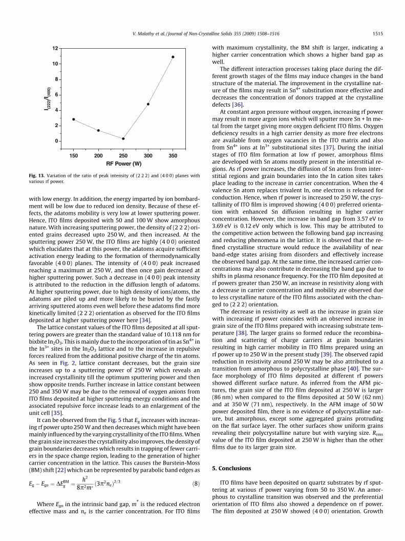
In the case of bixbite ITO films, the (2 2 2) plane is the most den-sely packed plane [33] accompanied with highest energy as well.The variation in the ratio of I(2 2 2)/I(4 0 0) with sputtering power isshown in Fig. 13. It shows a minimum at 250 W with increasingtrend on both sides of lower and higher power density. At lowersputtering power, the energy acquired by the sputtering inert Ar+
ions which are colliding on the target may be low due to relativelylower discharge voltage. This results in generating sputtered atoms
150 200 250 300 350
0
2
4
6
8
10
12I (2
22)/I
(400
)
RF Power (W)
Fig. 13. Variation of the ratio of peak intensity of (2 2 2) and (4 0 0) planes withvarious rf power.
V. Malathy et al. / Journal of Non-Crystalline Solids 355 (2009) 1508–1516 1515
with low energy. In addition, the energy imparted by ion bombard-ment will be low due to reduced ion density. Because of these ef-fects, the adatoms mobility is very low at lower sputtering power.Hence, ITO films deposited with 50 and 100 W show amorphousnature. With increasing sputtering power, the density of (2 2 2) ori-ented grains decreased upto 250 W, and then increased. At thesputtering power 250 W, the ITO films are highly (4 0 0) orientedwhich elucidates that at this power, the adatoms acquire sufficientactivation energy leading to the formation of thermodynamicallyfavorable (4 0 0) planes. The intensity of (4 0 0) peak increasedreaching a maximum at 250 W, and then once gain decreased athigher sputtering power. Such a decrease in (4 0 0) peak intensityis attributed to the reduction in the diffusion length of adatoms.At higher sputtering power, due to high density of ions/atoms, theadatoms are piled up and more likely to be buried by the fastlyarriving sputtered atoms even well before these adatoms find morekinetically limited (2 2 2) orientation as observed for the ITO filmsdeposited at higher sputtering power here [34].
The lattice constant values of the ITO films deposited at all sput-tering powers are greater than the standard value of 10.118 nm forbixbite In2O3. This is mainly due to the incorporation of tin as Sn4+ inthe In3+ sites in the In2O3 lattice and to the increase in repulsiveforces realized from the additional positive charge of the tin atoms.As seen in Fig. 2, lattice constant decreases, but the grain sizeincreases up to a sputtering power of 250 W which reveals anincreased crystallinity till the optimum sputtering power and thenshow opposite trends. Further increase in lattice constant between250 and 350 W may be due to the removal of oxygen anions fromITO films deposited at higher sputtering energy conditions and theassociated repulsive force increase leads to an enlargement of theunit cell [35].
It can be observed from the Fig. 5 that Eg increases with increas-ing rf power upto 250 W and then decreases which might have beenmainly influenced by the varying crystallinity of the ITO films. Whenthe grain size increases the crystallinity also improves, the density ofgrain boundaries decreases which results in trapping of fewer carri-ers in the space change region, leading to the generation of highercarrier concentration in the lattice. This causes the Burstein-Moss(BM) shift [22] which can be represented by parabolic band edges as
Eg � Ego ¼ DEBMg ¼ h2
8p2m�ð3p2neÞ2=3 ð8Þ
Where Ego in the intrinsic band gap, m* is the reduced electroneffective mass and ne is the carrier concentration. For ITO films
with maximum crystallinity, the BM shift is larger, indicating ahigher carrier concentration which shows a higher band gap aswell.
The different interaction processes taking place during the dif-ferent growth stages of the films may induce changes in the bandstructure of the material. The improvement in the crystalline nat-ure of the films may result in Sn4+ substitution more effective anddecreases the concentration of donors trapped at the crystallinedefects [36].
At constant argon pressure without oxygen, increasing rf powermay result in more argon ions which will sputter more Sn + In me-tal from the target giving more oxygen deficient ITO films. Oxygendeficiency results in a high carrier density as more free electronsare available from oxygen vacancies in the ITO matrix and alsofrom Sn4+ ions at In3+ substitutional sites [37]. During the initialstages of ITO film formation at low rf power, amorphous filmsare developed with Sn atoms mostly present in the interstitial re-gions. As rf power increases, the diffusion of Sn atoms from inter-stitial regions and grain boundaries into the In cation sites takesplace leading to the increase in carrier concentration. When the 4valence Sn atom replaces trivalent In, one electron is released forconduction. Hence, when rf power is increased to 250 W, the crys-tallinity of ITO film is improved showing (4 0 0) preferred orienta-tion with enhanced Sn diffusion resulting in higher carrierconcentration. However, the increase in band gap from 3.57 eV to3.69 eV is 0.12 eV only which is low. This may be attributed tothe competitive action between the following band gap increasingand reducing phenomena in the lattice. It is observed that the re-fined crystalline structure would reduce the availability of nearband-edge states arising from disorders and effectively increasethe observed band gap. At the same time, the increased carrier con-centrations may also contribute in decreasing the band gap due toshifts in plasma resonance frequency. For the ITO film deposited atrf powers greater than 250 W, an increase in resistivity along witha decrease in carrier concentration and mobility are observed dueto less crystalline nature of the ITO films associated with the chan-ged to (2 2 2) orientation.
The decrease in resistivity as well as the increase in grain sizewith increasing rf power coincides with an observed increase ingrain size of the ITO films prepared with increasing substrate tem-perature [38]. The larger grains so formed reduce the recombina-tion and scattering of charge carriers at grain boundariesresulting in high carrier mobility in ITO films prepared using anrf power up to 250 W in the present study [39]. The observed rapidreduction in resistivity around 250 W may be also attributed to atransition from amorphous to polycrystalline phase [40]. The sur-face morphology of ITO films deposited at different rf powersshowed different surface nature. As inferred from the AFM pic-tures, the grain size of the ITO film deposited at 250 W is larger(86 nm) when compared to the films deposited at 50 W (62 nm)and at 350 W (71 nm), respectively. In the AFM image of 50 Wpower deposited film, there is no evidence of polycrystalline nat-ure, but amorphous, except some aggregated grains protrudingon the flat surface layer. The other surfaces show uniform grainsrevealing their polycrystalline nature but with varying size. Rrms
value of the ITO film deposited at 250 W is higher than the otherfilms due to its larger grain size.
5. Conclusions
ITO films have been deposited on quartz substrates by rf sput-tering at various rf power varying from 50 to 350 W. An amor-phous to crystalline transition was observed and the preferentialorientation of ITO films also showed a dependence on rf power.The film deposited at 250 W showed (4 0 0) orientation. Growth
1516 V. Malathy et al. / Journal of Non-Crystalline Solids 355 (2009) 1508–1516
mechanism, for the films deposited below and above 250 W, fol-lowed the (2 2 2) orientation even when the films showed eitheramorphous or less crystalline nature. With the increase of rf power,the grain size and crystalline quality of ITO films were improved,the Hall mobility increased to a maximum of 8.3 cm2/vs and theresistivity decreased to a minimum of 4.3 � 10�3 X cm. The bandgap is 3.69 eV and the refractive index and low extinction coeffi-cient values in the visible region confirms the formation of highlycrystalline, void free and compact ITO films whose microstructuralparameters like strain and dislocation density are minimum at250 W. XPS study shows the substitution of In3+ sites with Sn4+
and EDX result reveals the uniform distribution of In and Sn onthe surface supported by the smoother surface with nano grainsas observed from AFM pictures. Through these results, it can beconfirmed that room temperature ITO films on quartz substrateswith 10�3 X cm and above 80% transmittance can be obtainedusing an rf power of 250 W at room temperature.
References
[1] C.G. Granqvist, A. Hultaker, Thin Solid Films 411 (2002) 1.[2] H. Kauazoe, M. Yasukawa, H. Hyodo, M. Kunita, H. Yanagi, H. Hosono, Nature
389 (1997) 939.[3] J.F. Nierengarten, G. Hadziioamnou, N. Armaroli, Mater. Today 4 (2001) 6.[4] G. Neri, A. Bonavita, G. Micali, G. Rizzo, N. Pinna, M. Niederberger, Thin Solid
Films 515 (2007) 8637.[5] H.L. Hartnagel, A.L. Dawar, A.K. Jain, C. Jagadish, Semiconducting Transparent
Thin Films, Institute of Physics, Bristol, 1995.[6] C.N. Carvalhio, A. Luis, O. Conde, E. Foitunato, G. Lavareda, A. Amaral, J. Non-
Cryst. Solids 299–302 (2002) 1208.[7] J. Herrero, C. Guillen, Vacuum 67 (2002) 611.[8] S. Ishibashi, Y. Higuchi, Y. Ota, K. Nakamura, J. Vac. Sci. Technol. A 8 (1990)
1399.[9] C.G. Granquist, Appl. Phys. A 52 (1991) 83.
[10] N.G. Patel, K.K. Makhija, C.J. Panchal, D.B. Dave, V.S. Vaishnav, Sens. Actuators B23 (1995) 49.
[11] W. Gopel, A.D. Amico, G. Sberveglieri (Eds.), in: Proceedings of the FirstEuropean School on Sensors (ESS94), World Scientific, 1995, p. 49.
[12] S. Venkatachalam, D. Mangalaraj, Sa.K. Narayandass, Physica B 393 (2007) 47.[13] E. Terzini, P. Thilakan, C. Minarini, Mater. Sci. Eng. B 77 (2000) 110.[14] P.K. Song, Y. Shigesato, M. Kamei, Jpn. J. Appl. Phys. 38 (1999) 2921.[15] H. Iozumi, F.O. Adurodiya, T. Kaneyoshi, T. Ishihara, H. Yoshioka, M. Motoyama,
J. Appl. Phys. 91 (2002) 1213.[16] F.E. Akkad, M. Marafi, A. Punnoose, G. Prahu, Phys. Stat. Sol. 177 (2000)
445.[17] H.R. Faliah, M. Ghasemi, A. Hassanzadeh, H. Steki, Physica B 383 (2006) 274.[18] J. George, C.S. Menon, Surf. Coat. Technol. 132 (2000) 45.[19] S. Ohmo, Y. Kawaguchi, A. Miyamma, Y. Sato, P.K. Song, M. Yoshikawa, P. Frech,
Y. Shigesarto, Sci. Technol. Adv. Mater. 7 (2006) 56.[20] L. Hao, X. Diao, H. Xu, B. Gu, T. Wang, Appl. Surf. Sci. 254 (2008) 3504.[21] J.R. Rani, V.P. Mahadevan Pillai, R.S. Ajimsha, M.K. Jayaraj, R.S. Jayashree, J.
Appl. Phys. 100 (2006) 014302.[22] E. Burstein, Phys. Rev. 93 (1954) 632.[23] J.C. Manifacier, M. De Municia, J.P. Fillard, E. Vicario, Thin Solid Films 41 (1977)
127.[24] R. Swanepoel, J. Phys. E: Sci. Instrum. 17 (1984) 896.[25] R. Swanepoel, J. Phys. E: Sci. Instrum. 16 (1983) 1214.[26] R. Das, K. Adhikary, S. Ray, Appl. Surf. Sci. 253 (2007) 6068.[27] S.J. Hong, J.I. Han, Curr. Appl. Phys. 681 (2006) 206.[28] S. Seki, Y. Sawada, T. Nishide, Thin Solid Films 338 (2001) 22.[29] A. Gurlo, N. Barsan, M. Ivanoskaya, U. Weiman, W. Gpel, Sens. Actuators B 47
(1998) 92.[30] S. Li, X. Qiao, J. Chen, Mater. Chem. Phys. 98 (2006) 144.[31] R.W. Smith, J. Appl. Phys. 81 (1997) 1196.[32] Y.S. Jung, S.S. Lee, J. Cryst. Growth 259 (2003) 343.[33] C.H. Yi, I. Yasui, Y. Shigesato, Jpn. J. Appl. Phys. 34 (1995) 1638.[34] H. Kim, J.S. Horwitz, G. Kushto, A. Pique, Z.H. Kafafi, C.M. Gilmore, D.B. Chrisey,
J. Appl. Phys. 88 (2000) 6021.[35] G.G. Gonzalez, J.B. Cohen, J.H. Hwang, T.O. Mason, J. Appl. Phys. 87 (2001)
2550.[36] L.J. Meng, A. Macarico, R. Martins, Vacuum 46 (1995) 673.[37] V. Teixeina, H.N. Cui, L.J. Meng, E. Fortunato, R. Mathins, Thin Solid Films 420–
421 (2002) 70.[38] S. Calnan, H.M. Upadhaya, M.J. Thwaites, A.N. Tiwari, Thin Solid Films 515
(2007) 6045.[39] J. Lee, H. Jung, D. Lim, K. Yang, W. Song, J. Li, Thin Solid Films 480–481 (2005)
157.[40] Y.S. Jung, D.W. Lee, D.Y. Jeon, Appl. Surf. Sci. 221 (2004) 136.