Embed Size (px)
Citation preview

July 14 2003 US LC Workshop Cornell U – Chris Damerell1
A CCD-based vertex detector
Chris Damerell on behalf of the LCFI Collaboration
• Project overview and design principles
• R&D programme
• Development of novel CCDs and readout electronics
• Development of thinnest possible detector layers
• Physics studies
• Summary and future plans
July 14 2003 US LC Workshop Cornell U – Chris Damerell2
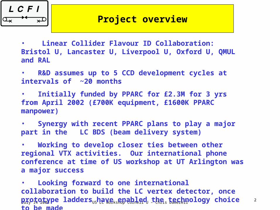
Project overview
• Linear Collider Flavour ID Collaboration: Bristol U, Lancaster U, Liverpool U, Oxford U, QMUL and RAL
• R&D assumes up to 5 CCD development cycles at intervals of ~20 months
• Initially funded by PPARC for £2.3M for 3 yrs from April 2002 (£700K equipment, £1600K PPARC manpower)
• Synergy with recent PPARC plans to play a major part in the LC BDS (beam delivery system)
• Working to develop closer ties between other regional VTX activities. Our international phone conference at time of US workshop at UT Arlington was a major success
• Looking forward to one international collaboration to build the LC vertex detector, once prototype ladders have enabled the technology choice to be made
• One major unknown in the decision process is the accelerator technology

July 14 2003 US LC Workshop Cornell U – Chris Damerell3
Design principles
• 5 layers, inner layer at radius 12-15 mm
• 3-hit coverage to cos= 0.96
• thin layers (<0.1% X0 ) for minimal mult scatt and conversions
July 14 2003 US LC Workshop Cornell U – Chris Damerell4
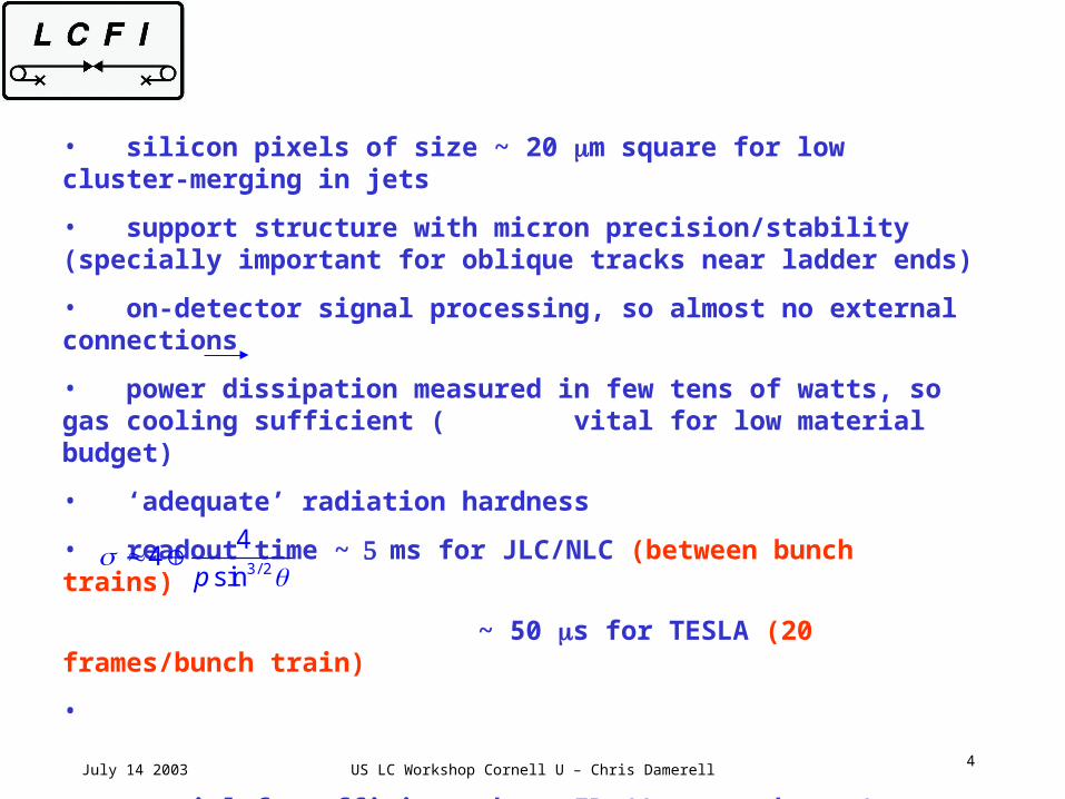
• silicon pixels of size ~ 20 m square for low cluster-merging in jets
• support structure with micron precision/stability (specially important for oblique tracks near ladder ends)
• on-detector signal processing, so almost no external connections
• power dissipation measured in few tens of watts, so gas cooling sufficient ( vital for low material budget)
• ‘adequate’ radiation hardness
• readout time ~ms for JLC/NLC (between bunch trains)
~ 50 s for TESLA (20 frames/bunch train)
•
• crucial for efficient charm ID (1-prong decays), vertex charge (Bs), but quantitative physics examples still being worked on …
3 2
44
/sinp
July 14 2003 US LC Workshop Cornell U – Chris Damerell5
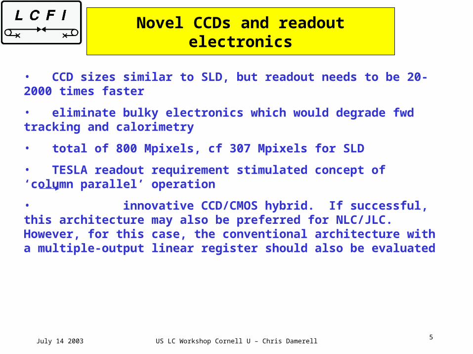
Novel CCDs and readout electronics
• CCD sizes similar to SLD, but readout needs to be 20-2000 times faster
• eliminate bulky electronics which would degrade fwd tracking and calorimetry
• total of 800 Mpixels, cf 307 Mpixels for SLD
• TESLA readout requirement stimulated concept of ‘column parallel’ operation
• innovative CCD/CMOS hybrid. If successful, this architecture may also be preferred for NLC/JLC. However, for this case, the conventional architecture with a multiple-output linear register should also be evaluated
July 14 2003 US LC Workshop Cornell U – Chris Damerell6
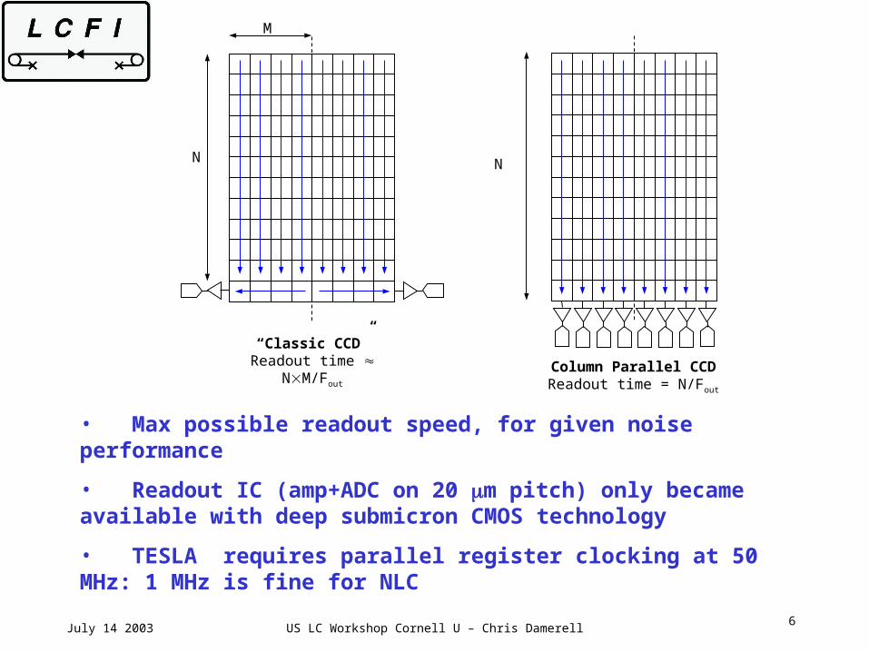
“Classic CCD”Readout time
NM/Fout
N
M
N
Column Parallel CCDReadout time = N/Fout
• Max possible readout speed, for given noise performance
• Readout IC (amp+ADC on 20 m pitch) only became available with deep submicron CMOS technology
• TESLA requires parallel register clocking at 50 MHz: 1 MHz is fine for NLC

July 14 2003 US LC Workshop Cornell U – Chris Damerell7
electronics only at the ends of the ladders
bump-bonded assembly between thinned CPCCD and readout chip
readout chip does all the signal processing, yielding sparsified digital data
CPCCD is driven with high frequency, low voltage clocks
low inductance layout required for clock delivery
July 14 2003 US LC Workshop Cornell U – Chris Damerell8
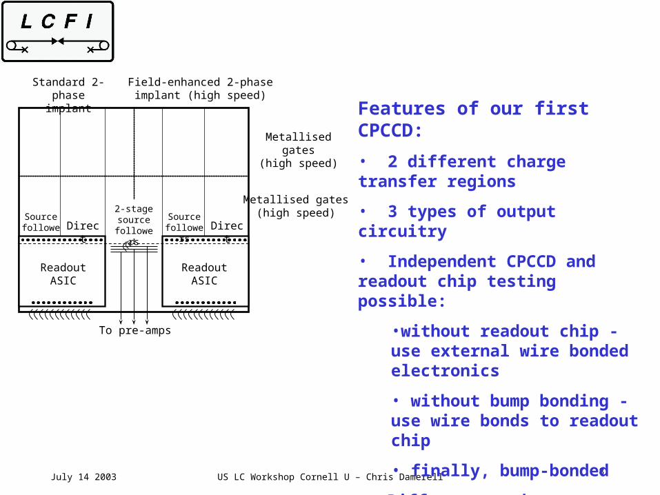
Standard 2-phaseimplant
Metallised gates(high speed)
Metallised gates(high speed)
Field-enhanced 2-phase implant (high speed)
Sourcefollowers
Sourcefollowers DirectDirect
2-stagesource
followers
To pre-amps
ReadoutASIC
ReadoutASIC
Features of our first CPCCD:
• 2 different charge transfer regions
• 3 types of output circuitry
• Independent CPCCD and readout chip testing possible:
•without readout chip - use external wire bonded electronics
• without bump bonding - use wire bonds to readout chip
• finally, bump-bonded
• Different readout concepts can be tested (direct charge sensing, and voltage sensing via source follower)
July 14 2003 US LC Workshop Cornell U – Chris Damerell9
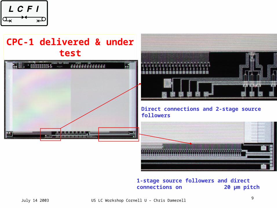
Direct connections and 2-stage source followers
1-stage source followers and direct connections on 20 μm pitch
CPC-1 delivered & under test

July 14 2003 US LC Workshop Cornell U – Chris Damerell10
July 14 2003 US LC Workshop Cornell U – Chris Damerell11
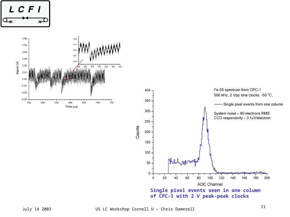
Single pixel events seen in one column of CPC-1 with 2 V peak-peak clocks

July 14 2003 US LC Workshop Cornell U – Chris Damerell12
FIFO
250 5-bit flash ADCs
Charge Amplifiers Voltage Amplifiers
Wire/bump bond pads
Wire/bump bond pads

July 14 2003 US LC Workshop Cornell U – Chris Damerell13
July 14 2003 US LC Workshop Cornell U – Chris Damerell14
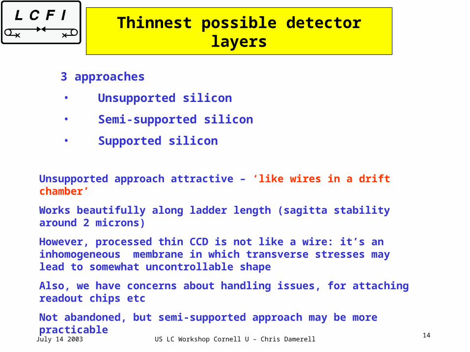
Thinnest possible detector layers
3 approaches
• Unsupported silicon
• Semi-supported silicon
• Supported silicon
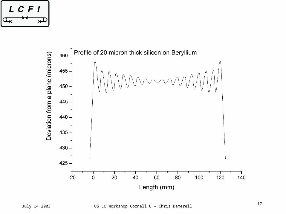
Unsupported approach attractive – ‘like wires in a drift chamber’
Works beautifully along ladder length (sagitta stability around 2 microns)
However, processed thin CCD is not like a wire: it’s an inhomogeneous membrane in which transverse stresses may lead to somewhat uncontrollable shape
Also, we have concerns about handling issues, for attaching readout chips etc
Not abandoned, but semi-supported approach may be more practicable

July 14 2003 US LC Workshop Cornell U – Chris Damerell15
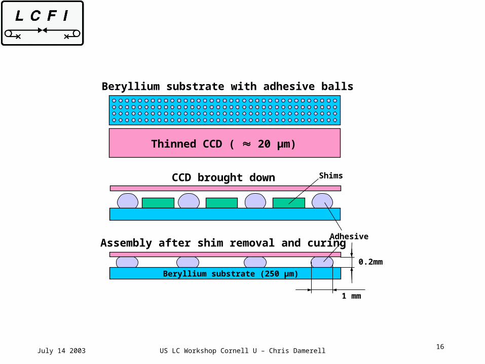
July 14 2003 US LC Workshop Cornell U – Chris Damerell16
CCD brought down
Assembly after shim removal and curing
Beryllium substrate (250 μm)
Beryllium substrate with adhesive balls
Thinned CCD ( 20 μm)
Adhesive
Shims
1 mm
0.2mm
July 14 2003 US LC Workshop Cornell U – Chris Damerell17

July 14 2003 US LC Workshop Cornell U – Chris Damerell18
Physics studies
The design of the VXD should be driven by the physics requirements:
• 4 configurations, 5 layer single thickness and 4 layer double thickness, and other combinations
• make single muon and pion tracks in Brahms for all momenta and angles. Fit the distributions
• include the parametrizations in Simdet
• biggest effect comes from removal of the inner layer
• provide to physics groups

July 14 2003 US LC Workshop Cornell U – Chris Damerell19
5layers4 layers,double
• Clear performance difference between configurations• Charm suffers most, B tagging is “easy”

July 14 2003 US LC Workshop Cornell U – Chris Damerell20
• New procedure to attach track to vertices
• Charged B, up to 89% correct tag, 6-8% worse for 4 layer double thickness configuration
• Charged D, excellent purity, less
difference between configurations
July 14 2003 US LC Workshop Cornell U – Chris Damerell21
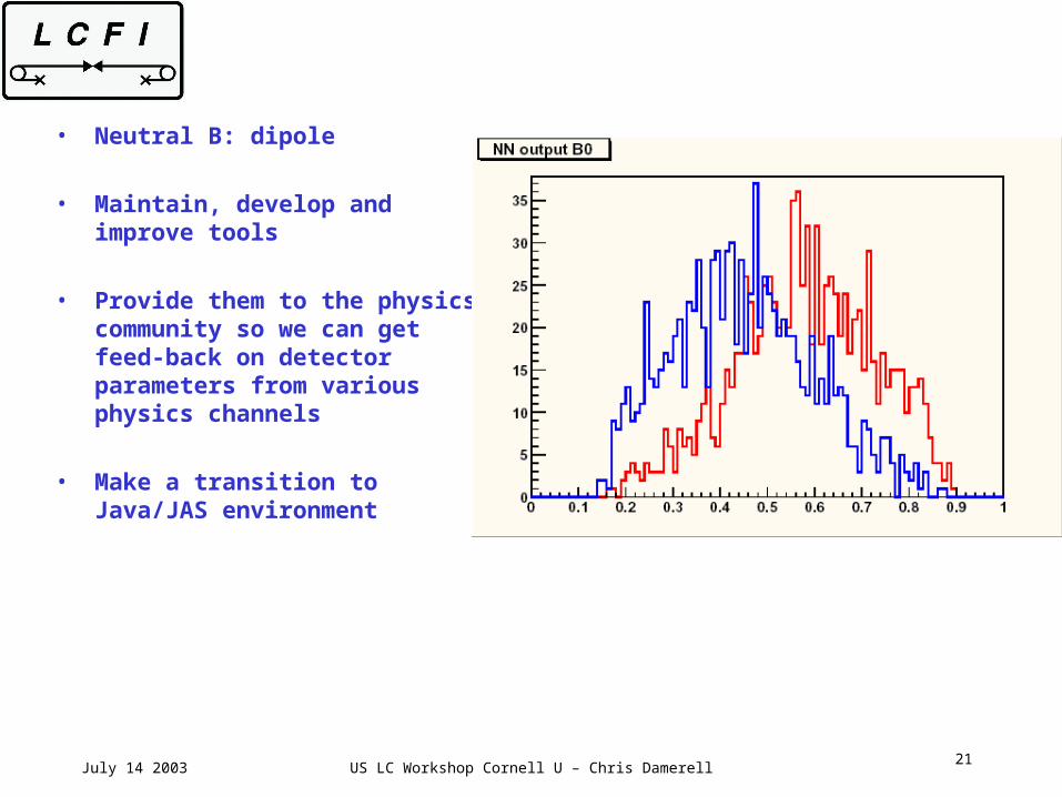
• Neutral B: dipole
• Maintain, develop and improve tools
• Provide them to the physics community so we can get feed-back on detector parameters from various physics channels
• Make a transition to Java/JAS environment

July 14 2003 US LC Workshop Cornell U – Chris Damerell22
Summary and future plans
• Fast CCDs:
• much to study with CPC-1
• tentative plan for design/production of CPC-2 (including detector-scale prototypes, 10x2 cm2) Oct 2003-June 2004
• readout chips CPR-1 and CPR-2 all we need in medium term future
• Thin ladders:
• semi-supported assemblies with a well-behaved adhesive may be fine, including satisfying the bump-bonding assembly requirements
• numerous alternative ideas, some (fortunately) being pursued by other groups – notably the DEPFET collaboration
• Physics studies:
• totally dependent on available effort, a small but dedicated team
• Major opportunities for wider collaboration in all areas, and informally it is happening


![knc/ 6] lcfi](https://img.pdfslide.net/doc/110x75/5d51cddd88c993c9398b5421/knc-6-lcfi.jpg)
