Embed Size (px)
Citation preview
67:1 (2014) 29–34 | www.jurnalteknologi.utm.my | eISSN 2180–3722 |
Full paper Jurnal
Teknologi
A Low-Voltage and Label-Free Impedance-based Miniaturized CMOS Biosensor for DNA Detection Vinny Lam Siu Fana, Wong How Hwana, Yusmeeraz Yusofa*
aFaculty of Electrical Engineering, Universiti Teknologi Malaysia, 81310 UTM Johor Bahru, Johor, Malaysia
*Corresponding author: [email protected]
Article history
Received :1 October 2013
Received in revised form :
4 January 2014 Accepted :30 January 2014
Graphical abstract
Abstract
This study designs a low-voltage, label-free and fully integrated impedance-based biosensor using standard
complementary metal oxide semiconductor (CMOS) technology to compute both capacitance and
resistance of the electrode-electrolyte interface. The proposed biosensor circuit is composed of a common-gate transimpedance amplifier (CG-TIA) with two quadrature phase Gilbert cell double-balanced mixers
and finally integrated with microelectrode using 0.18 µm Silterra CMOS technology process. The output
value of the readout circuit was used to estimate the magnitude and phase of the measured admittance. The developed CG-TIA can achieve a gain of 88.6 dB up to a frequency of 50 MHz. The overall dynamic range
was approximately 116 dB.
Keywords: CMOS; biosensor; impedance;lLabel-free DNA; low-voltage
Abstrak
Penyelidikan ini mereka satu impedans biosensor yang bervoltan rendah, penunjuk bebas dan boleh
disepadukan secara lengkap menggunakan teknologi CMOS untuk mengira kemuatan dan rintangan bagi
antara muka elektrod-elektrolit. Litar biosensor yang dicadangkan terdiri daripada CG-TIA dengan dua fasa
kuadratur Gilbert sel mixers dua seimbang dan akhirnya disepadukan dengan mikroelektrod menggunakan
0.18 µm proses teknologi Silterra CMOS. Nilai keluaran bagi litar bacaan akan digunakan untuk menganggarkan magnitud dan fasa kemasukan tersebut. CG-TIA yang dicadangkan telah mencapai
gandaan sebanyak 88.6 dB sehingga frekuensi 50 MHz. Julat dinamik keseluruhan adalah lebih kurang 116
dB.
Kata kunci: CMOS; biosensor; impedans; penunjuk bebas DNA; voltan rendah
© 2014 Penerbit UTM Press. All rights reserved.
1.0 INTRODUCTION
Deoxyribonucleic Acid (DNA) biosensor is a powerful tool that
utilizes the DNA hybridization procedures to detect the presence of
bacterial and virus diseases through the use of highly conserved
DNA sequences.1 These biological responses can be converted into
an electrical, chemical or acoustic signal. However, these rawest
form of signals are indigestible and require various detection
schemes to extract the relevant information.
Most conventional DNA biosensors are based on
fluorescence-based detection, which provides an excellent
selectivity and sensitivity. This method requires attachment of
visible markers to analytes and also needs high intensity sources,
optical filters and lenses, which made the system bulky, costly,
time-consuming and not suited for point-of-care (POC)
diagnostics. On the contrary, electrochemical biosensors allow
increased sensitivities, label-free, require short analysis time,
affordable and can be readily integrated using standard CMOS
process technology.2
Several types of electrochemical biosensors such as charge transfer
sensor, field-effect based sensor, capacitance-based sensor and
impedance-based sensor have been reported for detecting DNA
hybridization.3,4,5 For example, Schienle et al.3 proposed a fully
electronic DNA sensor by using the amperometric detection, where
the hybridization process was detected by means of the redox
current between the two interdigitated sensing electrodes from the
enzyme label of target DNA molecules. Meanwhile, Stagni et al.4
proposed another label-free capacitance-based DNA sensor that
used the change of capacitance between the electrolyte and
electrode as the detection of hybridization process. Among these
previous works, electrochemical impedance spectroscopy (EIS) is
more favorable due to its label-free and real-time detection
capabilities.
30 Vinny, Wong & Yusmeeraz / Jurnal Teknologi (Sciences & Engineering) 67:1 (2014), 29–34
2.0 PROBLEM STATEMENT
Several studies on the electrical detection of biomolecules based on
the changes in the electrical double layer properties of the
functionalized electrode surface have been proposed. Such systems
harness the unique impedance values from biomolecules such as
DNA, proteins and other cells.
One of the detection method based on this principle is
capacitive detection method.6,7 The notation ‘d’ from Figure 1
represents the distance between the polarized metal electrode and
the attracted ions for the capacitance. After double-stranded DNA
(ds-DNA) are formed due to hybridization event, the capacitance
of the double layer, CDL, decreases and the charge transfer
resistance, RCT, increases. However, the capacitive sensing does
not present enough stable capacitance properties as the measured
capacitance after the hybridization event may increase. As shown
in Figure 1, the flexible single-stranded DNA (ss-DNA) transforms
into a rigid rod upon binding and causes the ds-DNA to become
straight up to the surface. Under this condition, some ions are able
to access near to the electrode surface due to the opening space
between the ds-DNA.8,9,10 To overcome this problem, some efforts
have focused on the modification of the probe layer on the surface
of electrode.11,12
Therefore, the impedance-based biosensor that measures both
capacitance and resistance of the electrode-electrolyte interface
after hybridization event is able to provide a more stable and
accurate result compared to the capacitive detection method.
This paper proposes a low-voltage, label-free and fully
integrated impedance-based biosensor using standard CMOS
technology to compute both capacitance and resistance of the
electrode-electrolyte interface.
Figure 1 The DNA physical changes upon DNA hybridization8
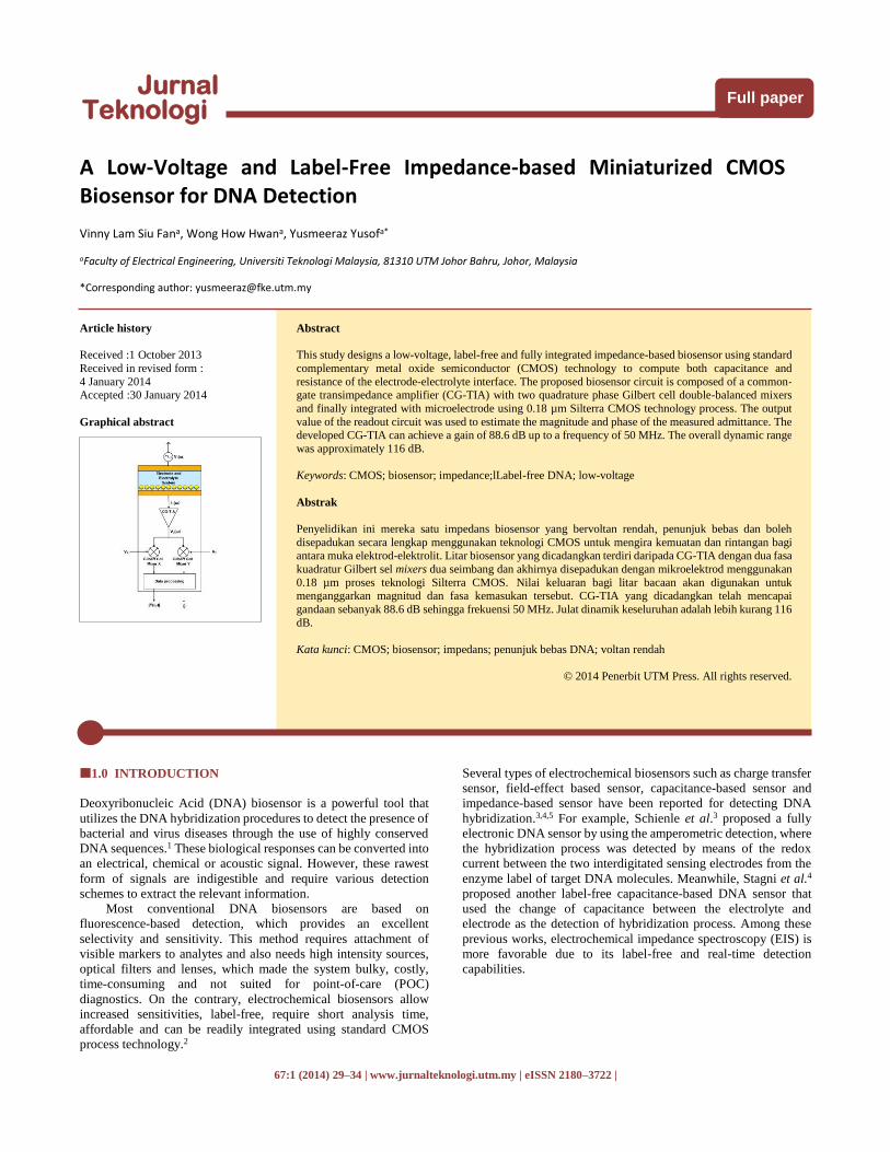
3.0 IMPEDANCE DETECTION SCHEME
Figure 2 shows the conceptual block diagram of EIS detection
method. A small excitation voltage, V1 (ω) was applied across the
electrode-electrolyte system and the magnitude and the phase of the
current flowing through the system was measured. The resulting
current I1 (ω) was amplified and converted to V2 (ω) using a low-
noise CG-TIA. The output voltage from CG-TIA, V2 (ω) was then
multiplied by an orthogonal sinusoidal signal (X or Y) at the
frequency ω. Signal Y is a quadrature phase of Signal X. Two DC
outputs, VX and VY, will be produced, which can be used to
estimate the magnitude, |Y (ω)| and phase φ, of the admittance
using Eq.(1) and Eq.(2):
4.0 CIRCUIT IMPLEMENTATION
As illustrated in Figure 3, the main components of the proposed
impedance-based readout circuit are a CG-TIA and two quadrature
phase Gilbert cell double-balanced mixers8 using 0.18µm Silterra
CMOS technology. The proposed low input impedance CG-TIA
consists of a common gate topology amplifier (MN1, MN2 and
MP1) with a gain boosting amplifier (MN3, MN4 and MP2). The
conversion gain can be boosted by enhancing the transconductance
of MN2 without sacrificing the signal bandwidth. The role of gain
boosting amplifier is not only to enhance the gain of TIA, but also
reduces the input impedance.
To multiply I1 (ω) by the X and Y quadrature signals, the
output voltage from CG-TIA, V2 (ω) was directly connected to the
input of two Gilbert cell mixers (MN5 – MN19) as shown in Figure
3.13 To avoid the mismatch of the input mixers, a replica of the TIA
(MN20-MN23, MP3-MP4) was designed and integrated within the
readout circuit. Under the operation of the mixer (X), the V2 (ω) voltage and the output voltage of the replica circuit were applied to
transistor MN6 and MN7 respectively, which performed a voltage
to current conversion. MN8 – MN12 formed a multiplication
function, multiplied the current from MN6 and MN7 with the X and
signal applied across MN8 – MN12, which provided the switching
function. MN6 and MN7 provided ± current and MN8 and MN12
switched between them to provide the inverted X signal to the left
hand load. MN9 and MN10 switched between them for the right
hand load. The two load resistors formed a current to voltage
transformation, giving differential output voltage, Vx. The same
operations above were applied to the mixer (Y). The load resistors
were realized by using active PMOS load in this design so that the
less layout area was used by the load resistor.
|𝑌(𝜔)| =√𝑉𝑋
2 + 𝑉𝑌2
𝐴𝐷| 𝑉1(𝜔)|
𝐴𝐷 =|𝑉2(𝜔)|
|𝐼1(𝜔)|
(1)
𝜙 = 𝑡𝑎𝑛−1(𝑉𝑌
𝑉𝑋) (2)
Figure 2 Impedance detection architecture
X Y
d d
VX VY
31 Vinny, Wong & Yusmeeraz / Jurnal Teknologi (Sciences & Engineering) 67:1 (2014), 29–34
The current through the CG-TIA with gain-boosting amplifier bias
current (I2) in this design is 7 µA. The bias current used in this
design was lower compared to the impedance-based biosensor
proposed by M. Arun14,15. This will allow the CG-TIA to achieve a
lower minimum detectable input current, which is 4.28 pA. The
overall current consumption of the readout circuit was 58 µA with
a 1.8 V supply.
Figure 3 The schematic of the proposed impedance-based readout circuit (excluding bias circuits)
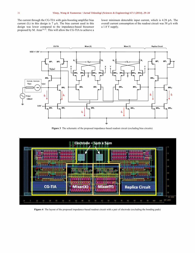
Figure 4 The layout of the proposed impedance-based readout circuit with a pair of electrode (excluding the bonding pads)
32 Vinny, Wong & Yusmeeraz / Jurnal Teknologi (Sciences & Engineering) 67:1 (2014), 29–34
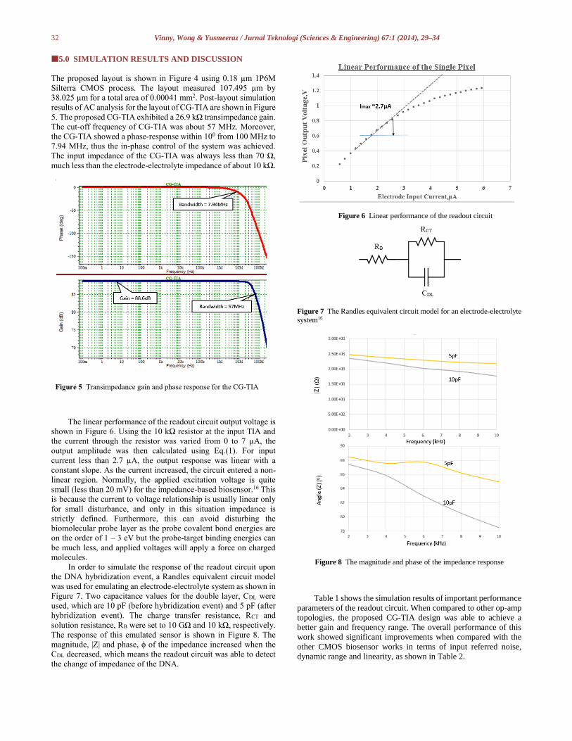
5.0 SIMULATION RESULTS AND DISCUSSION
The proposed layout is shown in Figure 4 using 0.18 µm 1P6M
Silterra CMOS process. The layout measured 107.495 µm by
38.025 µm for a total area of 0.00041 mm2. Post-layout simulation
results of AC analysis for the layout of CG-TIA are shown in Figure
5. The proposed CG-TIA exhibited a 26.9 kΩ transimpedance gain.
The cut-off frequency of CG-TIA was about 57 MHz. Moreover,
the CG-TIA showed a phase-response within 100 from 100 MHz to
7.94 MHz, thus the in-phase control of the system was achieved.
The input impedance of the CG-TIA was always less than 70 Ω,
much less than the electrode-electrolyte impedance of about 10 kΩ.
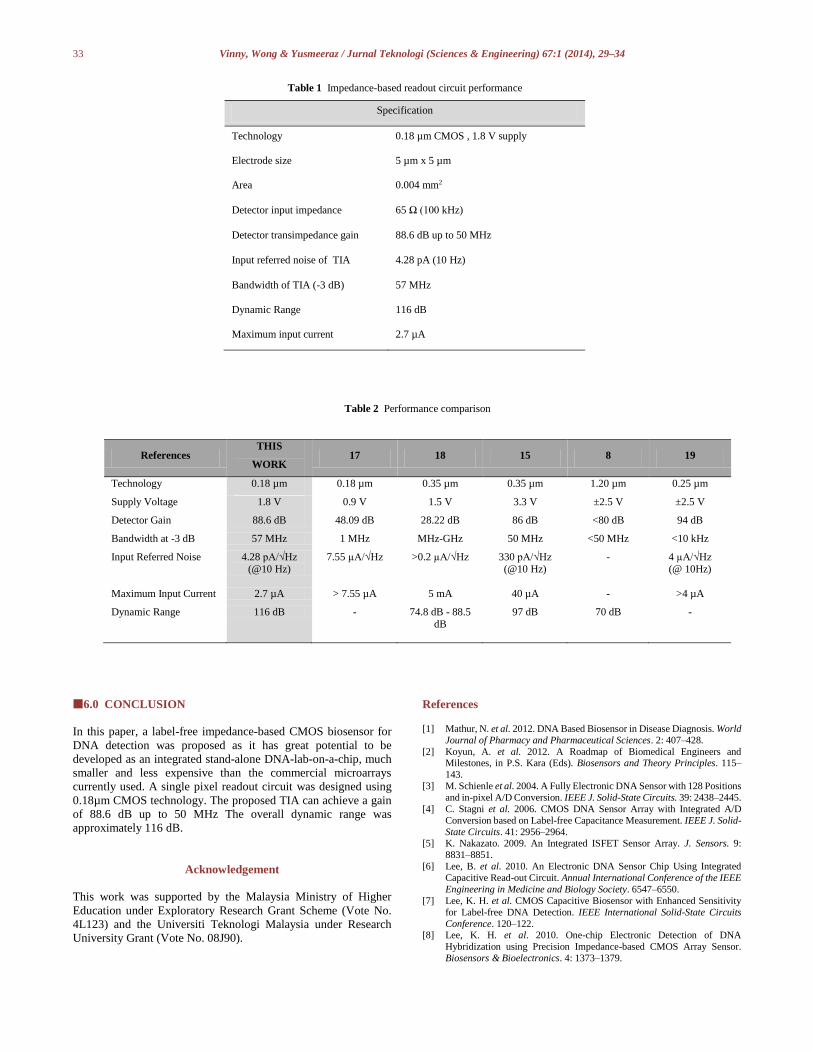
The linear performance of the readout circuit output voltage is
shown in Figure 6. Using the 10 kΩ resistor at the input TIA and
the current through the resistor was varied from 0 to 7 µA, the
output amplitude was then calculated using Eq.(1). For input
current less than 2.7 µA, the output response was linear with a
constant slope. As the current increased, the circuit entered a non-
linear region. Normally, the applied excitation voltage is quite
small (less than 20 mV) for the impedance-based biosensor.16 This
is because the current to voltage relationship is usually linear only
for small disturbance, and only in this situation impedance is
strictly defined. Furthermore, this can avoid disturbing the
biomolecular probe layer as the probe covalent bond energies are
on the order of 1 – 3 eV but the probe-target binding energies can
be much less, and applied voltages will apply a force on charged
molecules.
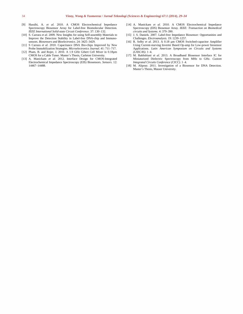
In order to simulate the response of the readout circuit upon
the DNA hybridization event, a Randles equivalent circuit model
was used for emulating an electrode-electrolyte system as shown in
Figure 7. Two capacitance values for the double layer, CDL were
used, which are 10 pF (before hybridization event) and 5 pF (after
hybridization event). The charge transfer resistance, RCT and
solution resistance, RB were set to 10 GΩ and 10 kΩ, respectively.
The response of this emulated sensor is shown in Figure 8. The
magnitude, |Z| and phase, ϕ of the impedance increased when the
CDL decreased, which means the readout circuit was able to detect
the change of impedance of the DNA.
Figure 7 The Randles equivalent circuit model for an electrode-electrolyte
system16
Figure 8 The magnitude and phase of the impedance response
Table 1 shows the simulation results of important performance
parameters of the readout circuit. When compared to other op-amp
topologies, the proposed CG-TIA design was able to achieve a
better gain and frequency range. The overall performance of this
work showed significant improvements when compared with the
other CMOS biosensor works in terms of input referred noise,
dynamic range and linearity, as shown in Table 2.
Figure 5 Transimpedance gain and phase response for the CG-TIA
Figure 6 Linear performance of the readout circuit
33 Vinny, Wong & Yusmeeraz / Jurnal Teknologi (Sciences & Engineering) 67:1 (2014), 29–34
6.0 CONCLUSION
In this paper, a label-free impedance-based CMOS biosensor for
DNA detection was proposed as it has great potential to be
developed as an integrated stand-alone DNA-lab-on-a-chip, much
smaller and less expensive than the commercial microarrays
currently used. A single pixel readout circuit was designed using
0.18µm CMOS technology. The proposed TIA can achieve a gain
of 88.6 dB up to 50 MHz The overall dynamic range was
approximately 116 dB.
Acknowledgement
This work was supported by the Malaysia Ministry of Higher
Education under Exploratory Research Grant Scheme (Vote No.
4L123) and the Universiti Teknologi Malaysia under Research
University Grant (Vote No. 08J90).
References [1] Mathur, N. et al. 2012. DNA Based Biosensor in Disease Diagnosis. World
Journal of Pharmacy and Pharmaceutical Sciences. 2: 407–428.
[2] Koyun, A. et al. 2012. A Roadmap of Biomedical Engineers and Milestones, in P.S. Kara (Eds). Biosensors and Theory Principles. 115–
143.
[3] M. Schienle et al. 2004. A Fully Electronic DNA Sensor with 128 Positions
and in-pixel A/D Conversion. IEEE J. Solid-State Circuits. 39: 2438–2445.
[4] C. Stagni et al. 2006. CMOS DNA Sensor Array with Integrated A/D
Conversion based on Label-free Capacitance Measurement. IEEE J. Solid-
State Circuits. 41: 2956–2964. [5] K. Nakazato. 2009. An Integrated ISFET Sensor Array. J. Sensors. 9:
8831–8851.
[6] Lee, B. et al. 2010. An Electronic DNA Sensor Chip Using Integrated
Capacitive Read-out Circuit. Annual International Conference of the IEEE
Engineering in Medicine and Biology Society. 6547–6550.
[7] Lee, K. H. et al. CMOS Capacitive Biosensor with Enhanced Sensitivity
for Label-free DNA Detection. IEEE International Solid-State Circuits
Conference. 120–122. [8] Lee, K. H. et al. 2010. One-chip Electronic Detection of DNA
Hybridization using Precision Impedance-based CMOS Array Sensor.
Biosensors & Bioelectronics. 4: 1373–1379.
Table 1 Impedance-based readout circuit performance
Specification
Technology 0.18 µm CMOS , 1.8 V supply
Electrode size 5 µm x 5 µm
Area 0.004 mm2
Detector input impedance 65 Ω (100 kHz)
Detector transimpedance gain 88.6 dB up to 50 MHz
Input referred noise of TIA 4.28 pA (10 Hz)
Bandwidth of TIA (-3 dB) 57 MHz
Dynamic Range 116 dB
Maximum input current 2.7 µA
Table 2 Performance comparison
References THIS
WORK 17 18 15 8 19
Technology 0.18 µm 0.18 µm 0.35 µm 0.35 µm 1.20 µm 0.25 µm
Supply Voltage 1.8 V 0.9 V 1.5 V 3.3 V ±2.5 V ±2.5 V
Detector Gain 88.6 dB 48.09 dB 28.22 dB 86 dB <80 dB 94 dB
Bandwidth at -3 dB 57 MHz 1 MHz MHz-GHz 50 MHz <50 MHz <10 kHz
Input Referred Noise 4.28 pA/√Hz (@10 Hz)
7.55 µA/√Hz
>0.2 µA/√Hz 330 pA/√Hz (@10 Hz)
- 4 µA/√Hz (@ 10Hz)
Maximum Input Current 2.7 µA > 7.55 µA 5 mA 40 µA - >4 µA
Dynamic Range 116 dB - 74.8 dB - 88.5 dB
97 dB 70 dB -
34 Vinny, Wong & Yusmeeraz / Jurnal Teknologi (Sciences & Engineering) 67:1 (2014), 29–34
[9] Hassibi, A. et al. 2010. A CMOS Electrochemical Impedance
Spectroscopy Biosensor Array for Label-free Biomolecular Detection.
IEEE International Solid-state Circuit Conference. 37: 130–132.
[10] S. Carrara et al. 2009. New Insights for using Self-assembly Materials to
Improve the Detection Stability in Label-free DNA-chip and Immuno-sensors. Biosensors and Bioelectronics. 24: 3425–3429.
[11] S Carrara et al. 2010. Capacitance DNA Bio-chips Improved by New
Probe Immobilization Strategies. Microelectronics Journal. 41: 711–717.
[12] Pham, B. and Rojer, J. 2010. A 1.9 GHz Gibert Cell Mixer in 0.18µm
CMOS for a Cable Tuner. Master’s Thesis, Carleton University.
[13] A. Manickam et al. 2012. Interface Design for CMOS-Integrated
Electrochemical Impedance Spectroscopy (EIS) Biosensors. Sensors. 12: 14467–14488.
[14] A. Manickam et al. 2010. A CMOS Electrochemical Impedance
Spectroscopy (EIS) Biosensor Array. IEEE: Transaction on Biomedical
circuits and Systems. 4: 379–390.
[15] J. S. Daniels. 2007. Label-free Impedance Biosensor: Opportunities and
Challenges. Electroanalysis. 19: 1239–1257. [16] R. Selby et al. 2013. A 0.18 µm CMOS Switched-capacitor Amplifier
Using Current-starving Inverter Based Op-amp for Low-power biosensor
Applications. Latin American Symposium on Circuits and Systems
(LASCAS). 1–4.
[17] M. Bakhshiani et al. 2013. A Broadband Biosensor Interface IC for
Miniaturized Dielectric Spectroscopy from MHz to GHz. Custom
Integrated Circuits Conference (CICC). 1–4. [18] M. Alipour. 2011. Investigation of a Biosensor for DNA Detection.
Master’s Thesis, Masser University.