Embed Size (px)
Citation preview

KALLEY SERVICE MANUAL
K-LED32HDST2
1. Caution…………………………………………………………………………
2. specification……………………………………………………………………
3. Alignment Procedure…………………………………………………………
4.Block diagram…………………………………………………………………
5.Scheme Diagram ……………………………………………………………
6. Troubleshooting………………………………………………………………
7. Explode drawing................................................................................................
This m anual i s t he l atest at t he t ime of pr inting, and doe s not include the modification which may be made after the printing, by the constant improvement of product

CA UTION: TO RE DUCE THE RIS K OFELECTR ICAL SHOCK, DO NOT REMOVECOVER (OR BACK). NO USER SERVICEABLEPAR TS INS IDE . RE FER SER VIC ING TOQUALIFIED SERVICE PERSONNEL.
The lighting flash with arrowhead symbol, with an equilateral triangle is intended to
alert the user to the presence of uninsulated voltage within the products
enclosure that may be of sufficient magnitude to constitute a risk of electric shock to
the person.
The exclamation point within an equilateral triangle is intended to alert the user to the
presence of important operating and maintenance (servicing) instructions in the
literature accompanying the appliance.
CAUTION:
Use of controls, adjustments or procedures other than those specified herein may result in
hazardous radiation exposure.
CAU T IONRISKRISK OF ELECTRIELECTRIC
SHOCKSHOCK DO NOTNOT OPEN.OPEN.
2
dangerous
WARNING: TO REDUCE RISK OF FIRE OR ELECTRIC SHOCK, DO NOTEXPOSE THIS APPLIANCE TO RAIN OR MOISTURE.
1. CAUTION
2

1. When the power cord or plug is damaged or frayed, unplug this television set from the wall outlet and refer servicing to
qualified service personnel.
2. Do not overload wall outlets and extension cords as this can result in fire or electric shock.
3. Do not allow anything to rest on or roll over the power cord, and do not place the TV where power cord is subject to
traffic or abuse. This may result in a shock or fire hazard.
4. Do not attempt to service this television set yourself as opening or removing covers may expose you to dangerous
voltage or other hazards. Refer all servicing to qualified service personnel.
5. Never push objects of any kind into this television set through cabinet slots as they may touch dangerous voltage
points or short out parts that could result in a fire or electric shock. Never spill liquid of any kind on the television set.
6. If the television set has been dropped or the cabinet has been damaged, unplug this television set from the wall outlet
and refer servicing to qualified service personnel.
7. If liquid has been spilled into the television set, unplug this television set from the wall outlet and refer servicing to
qualified service personnel.
8. Do not subject your television set to impact of any kind. Be particularly careful not to damage the picture tube surface.
9. Unplug this television set from the wall outlet before cleaning. Do not use liquid cleaners or aerosol cleaners. Use a
damp cloth for cleaning.
10.1. Do not place this television set on an unstable cart, stand, or table. The television set may fall, causing serious injury
to a child or an adult, and serious damage to the appliance. Use only with a cart or stand recommended by the
manufacturer, or sold with the television set. Wall or shelf mounting should follow the manufacturer s instructions, and
should use a mounting kit approved by the manufacturer.
10.2. An appliance and cart combination should be moved with care. Quick stops, excessive force, and uneven surfaces
may cause the appliance and cart combination to overturn.
CAUTION:
Read all of these instructions. Sa ve these instructions for later use . Follo w all Warnings and
Instructions marked on the audio equipment.
1. Read Instructions-All the safety and operating instructionsshouldbe read before the productis operated.
2. Retain Instructions- The safety and operating instructions should be retained for future reference.
3. Heed Warnings- All warnings on the productand in the operating instructions should be adhered to.
4. Follow Instructions- All operating and use instructions should be followed.
3
IMPORTANT SAFETY INSTRUCTIONS
FOR YOUR PERSONAL SAFETY
3

11. Do not use this television set near water ... for example, near a bathtub, washbowl, kitchen sink, or laundry tub, in a
wet basement, or near a swimming pool, etc.
Never expose the set to rain or water. If the set has been exposed to rain or water, unplug the set from the wall
outlet and refer servicing to qualified service personnel.
12. Choose a place where light (artificial or sunlight) does not shine directly on the screen.
13. Avoid dusty places, since piling up of dust inside TV chassis may cause failure of the set when high humidity persists.
14. The set has slots, or openings in the cabinet for ventilation purposes, to provide reliable operation of the receiver, to
protect it from overheating. These openings must not be blocked or covered.
Never cover the slots or openings with cloth or other material.
Never block the bottom ventilation slots of the set by placing it on a bed, sofa, rug, etc.
Never place the set near or over a radiator or heat register.
Never place the set in enclosure, unless proper ventilation is provided.
15.1. If an outside antenna is connected to the television set, be sure the antenna system is grounded so as to provide some
protection against voltage surges and built up static charges, Section 810 of the National Electrical Code, NFPA No.
70-1975, provides information with respect to proper grounding of the mast and supporting structure, grounding of the
lead-in wire to an antenna discharge unit, size of grounding conductors, location of antenna discharge unit, connection
to grounding electrode, and requirements for the grounding electrode.
15.2. Note to CATV system installer : (Only for the television set with CATV reception)
This reminder is provided to call the CATV system attention to Article 820-40 of the NEC that provides
guidelines for proper grounding and, in particular, specifies that the cable ground shall be connected to the grounding
system of the building, as close to the point of cable entry as practical.
16. An outside antenna system should not be located in the vicinity of overhead power lines or other electric lights or power
circuits, or where it can fall into such power lines or circuits. When installing an outside antenna system, extreme care
should be taken to keep from touching such power lines or circuits as contact with them might be fatal.
17. For added protection for this television set during a lightning storm, or when it is left unattended and unused for long
periods of time, unplug it from the wall outlet and disconnect the antenna. This will prevent damage due to lightning
and power-line surges.
ANTENNALEAD- IN WIRE
ANTENNA DISCHARGE
UNIT (NEC SECTION
810-20)
GROUNDING
CONDUCTORS
(NEC SECTION810-21)
GROUND CLAMPS
POWER SERVICE GROUNDING
ELECTRODE SYSTEM
(NEC ART 250. PART H)
ELECTRIC SERVICEEQUIPMENT
GROUND CLAMP
NEC-NATIONAL ELECTRICAL CODE
EXAMPLE OF ANTENNA GROUNDING AS PER
NATIONAL ELECTRICAL CODE
EXAMPLE OF ANTENNA GROUNDING AS PER NATIONAL ELECTRICAL CODE INSTRUCTIONS
a built-in
installer s
4
PROTECTION AND LOCATION OF YOUR SET
PROTECTION AND LOCATION OF YOUR SET
4

18. This television set should be operated only from the type of power source indicated on the marking label.If you are not
sure of the type of power supply at your home, consult your television dealer or local power company. For television
sets designed to operate from battery power, refer to the operating instructions.
19. If the television set does not operate normally by following the operating instructions, unplug this television set from the
wall outlet and refer servicing to qualified service personnel. Adjust only those controls that are covered in the operating
instructions as improper adjustment of other controls may result in damage and will often require extensive work by a
qualified technician to restore the television set to normal operation.
20. When going on a holiday : If your television set is to remain unused for a period of time, for instance, when you go on
a holiday, turn the television set and unplug the television set from the wall outlet.
21. If you are unable to restorenormal operationby followingthe detailedprocedurein youroperatinginstructions,
do not attempt any further adjustment. Unplug the set and call your dealer or service technician.
22. Whenever the television set is damaged or fails, or a distinct change in performance indicates a need for
service, unplug the set and have it checked by a professional service technician.
23. It is normal for some TV sets to make occasional snapping or popping sounds, particularly when being
turned on or off. If the snapping or popping is continuous or frequent, unplug the set and consult your
dealer or service technician.
24. Do not use attachments not recommendedby the television set manufacturer as they may cause hazards.
25. When replacementparts are required,be sure the service technicianhas used replacementparts specified
by the manufacturer that have the same characteristics as the original part. Unauthorized substitutions
may result in fire, electric shock, or other hazards.
26. Upon completion of any service or repairs to the television set, ask the service technician to perform
routine safety checks to determine that the television is in safe operating condition.
off
5
OPERATION OF YOUR SET
IF THE SET DOES NOT OPERATE PROPERLY
FOR SERVICE AND MODIFICATION
5

Product Type LCD Smart TV Music support MP3/AC3/HE-AAC/LPCM/WMAChassis MS08GP-LA Picture Support JPEG、BMP、PNG、MPOCPU 1GHZ Support H.264、MPEG1、MPEG2、
MPEG4GPU --- Motion JPEG/VC1OS Linux
Memory Bein 2Gb DDR3 +External 1Gb DDR3/ 2GbNandFlash File ---
OSD Language English/Portuguese/SpanishPAL-M/N ;NTSC-MDVB-T2
AV System PAL,NTSC DVI Video Format Up to XGA for HDMI-PCChannels(Analog) Antenna:2~69;CATV:1~125 HDMI Video Format up to 1080PDTV Channels DVB-T2 Antenna:14~69 PC Compatibility Up to SXGAPower Supply AC 110V-240V 50/60Hz
Power Consumption(TV On) 45W
Power Consumption(Standby) ≤0.5W Backlight Unit LEDCertification CB Panel supplier CSOT(ST3151A05-8)Energy Efficiency Level --- Aspect Ratio 16:9
Wired Network Default Panel Size (inch) 31.5"Built-in Wi-Fi Network Display Resolution 1366*768
Brightness (cd/m2)(typ.) 240Contrast Ratio 3000:1Response Time (G to G) 6.5ms
EPG Yes(at DTV) Viewing Angle (H/V) 178°/178°Subtitle Yes(at DTV) Life Time(Typ.) >30,000hrsParental Control Yes(at DTV) Color 16.7 M(8bit)Lock Yes Refresh Rate 60HzV-Chip ---CCD (Closed Caption) Yes
Sleep Timer YesTeletext NoNicam No Side MTS YesScreen Saver YesSystem Update YesHotel Mode Optional(In factory mode)
REC YesAnalog / Digital Signal Receiver YesMHL ---Card Reader ---TimeShift YesOff Timers Yes
Natura Light Technology ---DCC(Dynamic Contrast Control) ON/OFFBacklight Adjustable Yes (0~100)Color Temperature Warm / Normal/ CoolPicture Mode Normal, Mid, Vivid, UserPicture Size Auto,16:9,4:3,Just ScanGamma Adjustable ---Comb Filter 3DDynamic Noise Reduction 3DAdaptive Deinterlacing 3DMotion Compensation Yes
Basic Function
Picture
Terminals
Special Function
PRODUCT SPECIFICATION RELEASEModel: K-LED32HDST2/MS08GP-LA/Smart TV/CSFGTA
Version:1.0 Issued On: 2015-2-5
Internet Link
Signal Format Capability
Panel Specification
Video
Basic Information Media Format
TV System
1
2
3
4

Sound Scene ---Surround Sound YesDD (Dolby Digital ) YesDobly DD+ Yes
Down
Twitter YesFacebook YesWeb Browser YesYouTube V4 YesOpera TV Store YesNETFLIX YesFile Share Yes
Wireless Display Yes
picasa Yes
Mechanical ID Picture
Pre-Installed Application List
Unit: mm
Unit: mm
Speakers Integrated speakers (Bottom Side) Audio Power Output(THD=7%) 2×5WSmart Volume Yes(Built-in)Smart Audio Normal,Music,Movie,News,UserSound Control Volume, Balance,5 Band EQ
5
Sound

Mechanical Key SpecificationCarton Dimensions LxWxH(mm) 851*136*531
Container Loading---20 feet(pcs) 472
Container Loading---40 feet(pcs) 1004
Container Loading--40 feet High(pcs) 1180
Net Weight With Stand(Kg) 4.8
Net Weight Without Stand(Kg) 4.7
Gross Weight With Packaging(Kg) 6.1(普通纸箱)
VESA Mounting Dimensions LxH(mm) 200X150
Operation Manual English(Default) Wall Mount WMB233
Remote Control and batteries RC199E(with two batteries) Wireless Keyboard ---
Base Stand Integrated Packaging Wireless Mouse ---
AC power cord 1 pc Game Controller ---
Drafted by: gongjunzan Approved by:
Design and specifications are subject to change without notice!
Optional AccessoriesEssential Accessories(Default)
Remote ID Picture
81MM
177MM
483MM
432.3MM
16.1MM
16.1MM
18.5MM
736MM

Alignment Procedure
MS08GP Series
MODEL:L32D2700/L40D2700
VERSION:V1.0
PREPARED BY : Gongjunzan DATE : 2015-3-23
APPROVED BY : DATE :

History Description of major changes Release
Date
Changed by
V1.0 2015-3-23
1.Overview
MS08GP These chassis are designed for Eastern Europe markets Ready for IPTV. The main chip is from Mstar and supports below features matrix:
2.Factory Menu
1、Methods of Entering
Method 1:Using the remote ,
Select “Picture” and press “OK” key to enter into Picture Mode press RIGHT” or “LEFT” key Select User Mode
- Press the subsequence RCU keys “9”, “7”, “3” and “5”,will appear in the left top of screen
In case of “Factory hotKey” is enabled(On), just press RCU “Return” key to pop-up again the Factory menu.
The status of “Factory Key” can be changed in Factory Menu->Hotkey. Press RCU “OK” key or “RIGHT” key to enter the submenu. Press RCU “Menu” key to go back to the root menu. Press RCU “RIGHT” or “LEFT” key to change the values. Press RCU “OK” key run the function. Press RCU “Exit” key exit the Factory menu.
2. General introduction
FACTORY MENU

ITEMS Default
Setting Description
St
at
us
1-Factory hotkey Off Factory hotkey Switch (OFF/ON).Should be OFF
after factory alignment OK
2-WARM-UP Off
OFF:The set would enter standby mode after
15 minutes without input signal;
ON:Aging mode. Aging time will display on
the left bottom of screen.
NOTE: Enter and exit the aging mode method: 1, press on the remote control Left and right the cursor keys will Factory hotkey set to ON; 2, WARM UP is set to ON; according to the panel on the "menu" button to exit the aging mode
OK
3-ADC ADC calibration(refer as follow),NOTE: Not
adjust
OK
4-White balance White Balance data adjustment ( refer as
follow)
The balance data is set by PE before the mass
production. Do not need adjust.
OK
5-SHOP
init(Option)
DO Reset the set after production
alignment;(This operation will remove all
unnecessary factory value; The factory
hotkey will be turn off)
OK
6-NVM reset DO System initialization. Restore all data
except the White Balance and ADC data ;Only
for R&D.
OK
7-Preset Factory
Channel
DO/HZ Preset specific factory channels for
specific factory. Press left and right
button to select the factory, and then press
OK to confirm.
OK
8-Power on mode LAST On: Always turns on TV when AC power on
STB:Always goes to standby mode when AC power
on
LAST:Restore the status before the last AC
power off
OK

9-USB
UPDATE(option)
USB update,(refer as follow)
Sub-item Value NotMain Upgrade Upgrade software
MEMC Upgrade Upgrade MEMC
HDCP Uprade Upgrade HDCP
Mboot upgrade Upgrade Mboot
CI KEY Upgrate Upgrade CI KEY
NVM Upgrade Upgrade NVM
NVM backup Backup NVM
CH list Upgrade Upgrade CH list
CH list backup Backup CH list
NetflixESN Upgrade Upgrade ESN
MAC Upgrade Upgrade MAC Add
OK
10—Deviceld test This item only factory used,
Note: Below the factory menu, some model information are showed, including
software version, Project Name, SIACP Version, and SW release time.
3)ADC Submenu:
NOTE: ADC Date use Default Setting, do without adjust
4)WHITE BALANCE Submenu
ITEMS Default
Setting
Description Statu
s
Source Current
Source
Current Source( HDMI1 need adjustment, Other
Source not use)
OK
COLOR TEMP NORMAL Medium/Cool/Ware OK
R gain 128 R-GAIN OK
G gain 128 G-GAIN OK
B gain 128 B-GAIN OK
White
Balance
init
DO ONLY FOR TCL R&D OK
NOTE:The first step is to adjust HDMI1
3.Design Menu

1、Methods of Entering:
Method 1:Using the remote, enter the “Picture” submenu in the OSD; choosing
the “contrast” item and press the 1,9,5,and 0 in series ,Design Menu will
appear in the left top of screen.
Method 2: Press RETURN button when DESIGN HOTKEY is enabled (ON).
2、General introduction
DESIGN MENU
ITEMS Default
Setting
Description Status
DESIGN
HOTKEY
OFF ON/OFF OK
1-FACTORY
MENU
ON/OFF OK
2-SHOP
Setting
Default setting submenu after production
alignment refer to **
OK
3-Other
Setting
Other set .Only for TCL R&D OK
4-SERVICE
menu
After service menu description OK
5-PARAM
SETTING
Parameter setting submenu OK
6-HOTEL MENU Hotel submenu(not adjust)
OK
SHOP INIT submenu
ITEMS Default
Setting
Description Status
Volume 30 0-100 adjustable OK
PIC MODE STANDARD Normal/Vivid/Mild/User OK
SOUND MODE STEREO Movie/news/Normal/Music/User OK
OSD
Language
English Up to 10 languages optional OK
Preset CH 1 0-199 adjustable OK
Color Temp Normal Normal/warm/cool
Sale Mode Home Mode
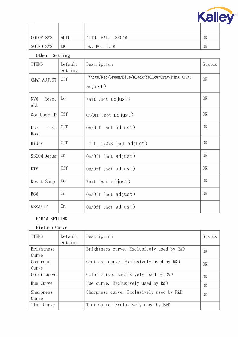
COLOR SYS AUTO AUTO、PAL、 SECAM OK
SOUND SYS DK DK、BG、I、M OK
Other Setting
ITEMS Default
Setting
Description Status
QMAP AUJUST Off White/Red/Green/Blue/Black/Yellow/Gray/Pink(not
adjust)
OK
NVM Reset
ALL
Do Wait(not adjust) OK
Got User ID Off On/Off(not adjust) OK
Use Test
Host
Off On/Off(not adjust) OK
Hidev Off Off..1\2\3(not adjust) OK
SSCOM Debug on On/Off(not adjust) OK
DTV Off On/Off(not adjust) OK
Reset Shop Do Wait(not adjust) OK
BGM On On/Off(not adjust) OK
WSS&ATF On On/Off(not adjust)
PARAM SETTING
Picture Curve
ITEMS Default
Setting
Description Status
Brightness
Curve
Brightness curve. Exclusively used by R&D OK
Contrast
Curve
Contrast curve. Exclusively used by R&D OK
Color Curve Color curve. Exclusively used by R&D OK
Hue Curve Hue curve. Exclusively used by R&D OK
Sharpness
Curve
Sharpness curve. Exclusively used by R&D OK
Tint Curve Tint Curve. Exclusively used by R&D

BackLight
Curve
BackLight curve. Exclusively used by R&D OK
OverScan Exclusively used by R&D
Sound Curve
Volume
Curve
Volume curve. Exclusively used by R&D OK
SSC adjust
SSC >>> SSC adjust . Exclusively used by R&D
Overscan Adjust
Over Scan Over Scan Exclusively used by R&D
DBC
DBC DBC Exclusively used by R&D
Back Light Curce
Back Curve Back curve. Exclusively used by R&D OK
Audio amp Setting
Audio
amp
Setting
Audio amp Setting
. Exclusively used by R&D
OK
DTV Para Setting
DTV Para
Setting
DTV Para Setting
. Exclusively used by R&D
OK
Hotel menu
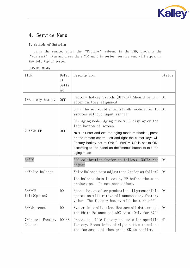
4、Service Menu
1、Methods of Entering
Using the remote, enter the “Picture” submenu in the OSD; choosing the
“contrast” item and press the 9,7,0 and 5 in series, Service Menu will appear in
the left top of screen
SERVICE MENU:
ITEM Defau
lt
Setti
ng
Description Status
1-Factory hotkey Off Factory hotkey Switch (OFF/ON).Should be OFF
after factory alignment
OK
2-WARM-UP Off
OFF:The set would enter standby mode after 15
minutes without input signal;
ON:Aging mode. Aging time will display on the
left bottom of screen.
NOTE: Enter and exit the aging mode method: 1, press on the remote control Left and right the cursor keys will Factory hotkey set to ON; 2, WARM UP is set to ON; according to the panel on the "menu" button to exit the aging mode
OK
3-ADC ADC calibration(refer as follow),NOTE: Not
adjust
OK
4-White balance White Balance data adjustment(refer as follow)
The balance data is set by PE before the mass
production. Do not need adjust.
OK
5-SHOP
init(Option)
DO Reset the set after production alignment;(This
operation will remove all unnecessary factory
value; The factory hotkey will be turn off)
OK
6-NVM reset DO System initialization. Restore all data except
the White Balance and ADC data ;Only for R&D.
OK
7-Preset Factory
Channel
DO/HZ Preset specific factory channels for specific
factory. Press left and right button to select
the factory, and then press OK to confirm.
NG

8-Power on mode LAST On: Always turns on TV when AC power on
STB:Always goes to standby mode when AC power
on
LAST:Restore the status before the last AC
power off
OK
9-USB
UPDATE(option)
USB update,(refer as follow)
Sub-item Value NoteMain Upgrade Upgrade software
MEMC Upgrade Upgrade MEMC
HDCP Uprade Upgrade HDCP
Mboot upgrade Upgrade Mboot
CI KEY Upgrate Upgrade CI KEY
NVM Upgrade Upgrade NVM
NVM backup Backup NVM
CH list Upgrade Upgrade CH list
CH list backup Backup CH list
NetflixESN Upgrade Upgrade ESN
MAC Upgrade Upgrade MAC Addre
10—Deviceld test This item only factory used, ok
5. Debugging
5.1. General Steps of debugging
According to the requirement of the order, below steps are needed for
appropriate setting.
1) Enter the Factory Menu, enable FAC HOTKEY.
2) Check Project ID and the version of software, release date displayed
at the bottom of Factory Menu.
3) Enter Design Menu, choose SERVICE MENU->Project ID, choose
corresponding Project ID number of the product (Refer to the
“V6-PROJECT -ID0**”in the BOM list).
4) Return to Factory Menu, check the Product model.
5) Choose Factory Menu->NVM RESET and press the right button of the
remote and wait until prompt OK appears.
6) Restart the set
7) According to the requirement of the order, Set the items of SHOP
INIT and Hotel Menu etc.

8)
9) Choose Factory Menu ->SHOP and press the button of remote to
initialize the set.
Note: After step 9, Hotel Menu will be disabled by default. Therefore,
if the order requires hotel function, it is necessary to enable hotel
function by set Design MENU->Service Menu->HOTEL ENABLE to ON.
5.2. Equipments
·Color Analyzer CA-210.
·Video Pattern Generator Chroma2329.
·Color TV Pattern Generator PM5418/Fluke5418.
·VGA cable , AV(RCA) cable , HDMI cable etc.
5.3. ADC Function not Calibration
5.4. White Balance adjustments (Manual)
Before adjustment ,you must make sure the ADC status(only PC and YPbPr)
is “success”and Color Analyzer has been calibrated .Only
AV1,YPbPr,PC,HDMI1 need to be adjusted. HDMI1 should be the first.
5.4.1. Signal and generator
The pattern of the signal should be used are White (Chroma2329 pattern
113) and Grey (pattern 114).
The format of signal are respectively 720P for HDMI1 (Chroma2329
Timing 69),PAL (Chroma2329 Timing38) for AV1,1024X768@60Hz(Chroma2329
Timing14) for VGA 。
5.4.2. Steps of adjustment
1).Enter the factory menu-> White Balance, select source HDMI 1 and
Normal Temperature.
2).Input grey signal in 720p format.
3).Change R-OFFSET and B-OFFSET to make sure the value of color
coordination equal to (X=0.270 +/-0.015;Y=0.290 +/-0.015).
4).Input white signal in 720p format.
5). Change R-GAIN and B-GAIN to make sure the value of color
coordination equal to (X=0.270 +/-0.015;Y=0.290 +/-0.015).
After aging under normal temperature, calibrate ADC and adjust
white balance.

6).Repeat step 2—5 until both of the value of color coordination of
white and grey equal to (X=0.270 +/-0.015;Y=0.290 +/-0.015).
For COOL and WARM color temperature, just repeat step 2—5.The color
coordination we recommend for COOL and WARM color temperature is
respectively(X=0.270 +/-0.015;Y=0.270 +/-0.015) and
(X=0.300 +/-0.015;Y=0.305 +/-0.015).
After the adjustment of HDMI1, you can switch to other source AV, PC
and YPbPr and repeat step 1—6 to do the WB adjustment.
Note: For some small size LED panel,the color coordination of specifications is not X=0.270/Y=0.290,and we recommend you adopt the values from panel specifications.
5.5. ADC Calibration and White Balance Adjustment (automatic)
The process of adjusting White Balance automatically is out of the
range of this file, Please refer to the relevant technical file of HuiZhou
factory of TCL.
6.Chip list of software programming before SMT
Following chips must be programmed before SMT by tools
Position Chip type Software description
U301 MT29F2G08ABAEA HDMI HDCP Key, System Software etc.
7.Software update
Method of SW update:
1) Download the bin file to the root directory of your USB device (Do
not change the file name); Then insert the USB device to USB interface
of TV set.
MS08GPSeries with its upgrade file corresponding relation as thetable
below show:
Chassis Name Sales
area Upgrade filename Remark
MS08GP LA MS08GP_MAIN.bin DVB-T2
2)Appendix “How to upgrade SW FLASH using Mstar tool”
See Appendix “How to upgrade MBOOT using USB”
Appendix “How to upgrade FLASH SW using USB”
Copy the SW BIN image “MS08GP_MBOOT.bin” into USB stick root path.Note: If there’s already other “MS08GP_MBOOT.bin” into USB root, it needs to be deleted

or renamed. Plug USB stick to the TV USB slot.Press RCU MENU Option Software upgrade By USB Confirm.Or, turn off the TV press and hold the power key of key board before reconnect ACcord to restart TV for 5-8seconds (Forced Upgrade).When the "UPGRADING SOFTWARE" picture appears as below, it means TV isuploading SW BIN image. Waiting a few minutes.
When updating is successful, TV should restart automatically.There are two methods to upgrade SW using USB, the first one like below: In the previous of upgrade SW using USB, should program mboot bin file” MS08GP_MBOOT.bin” by ISP_Tool or by USB. .
Then switch off TV by removing AC cord.Copy the SW BIN image “MS08GP_MAIN.bin” for MS08GP into USB stick (pen
drive) root path
Note: If there’s already other “The same name ” into USB root, it needs to be deleted or renamed Plug USB stick to the TVPress and hold the power key of key board before reconnect AC cord to restart
TV for 5-8seconds. Once USB stick starts blinking, TV is uploading SW BIN image.When update is successful, TV should restart automatically.Remember to perform “Factory menu NVM reset“ and then press RCU “OK”
key Switch off TV by removing AC cordReconnect AC cord to restart TV and wait few seconds for Eeprom update
The second method: To use this method, there should be SW in mainboard to ensure TV can display
normally. Copy the SW BIN image “MS08GP_MAIN.bin” and into USB stick (pen drive)
root path Press RCU MENU Option Software upgrade By USB ConfirmTV display warning information, that means it is upgrading, almost 3minutes later,
when upgrade successful, TV should restart automatically.

Appendix “How to change ProjectID with RCU”
Process following subsequence IR codes to change project ID:062598+MENU+xxx (xxx: Project ID, ex: 001)Restart TV
Appendix “How to upgrade MAC Address
Upgrading MAC address need to use the tool in factory and through serialcommand, the specific methods according to the operation of the factoryguidance.
Appendix “Instructions of Updating SW”
1. The following IC should be pre-copied before SMT process
Position PART TYPE Part Number SW U301
(CPP)IC-TSOP48 13-FS29F2-G0B Mboot, Main Software
2. The MAC Address, HDCP KEY, Device ID must be upgrade by debug portinto U301.
8, Project ID selecting
1) Press the Menu button of remote control, then select Contrast itemof Picture submenu; press 1,9,5,0 consecutively, there you go the
Design Menu.
2) Select the SERVICE MENU item, press OK and RIGHT button of the remote
to enter submenu,
3) Select the PROJECT ID item, press OK or RIGHT button of the remoteto enter the submenu;
4) Press the right or left button of the remote to select the ID you want;
5) After ID selection, press MENU button of the remote to exit DESIGNMENU.
6) Finally, do AC power on/off.

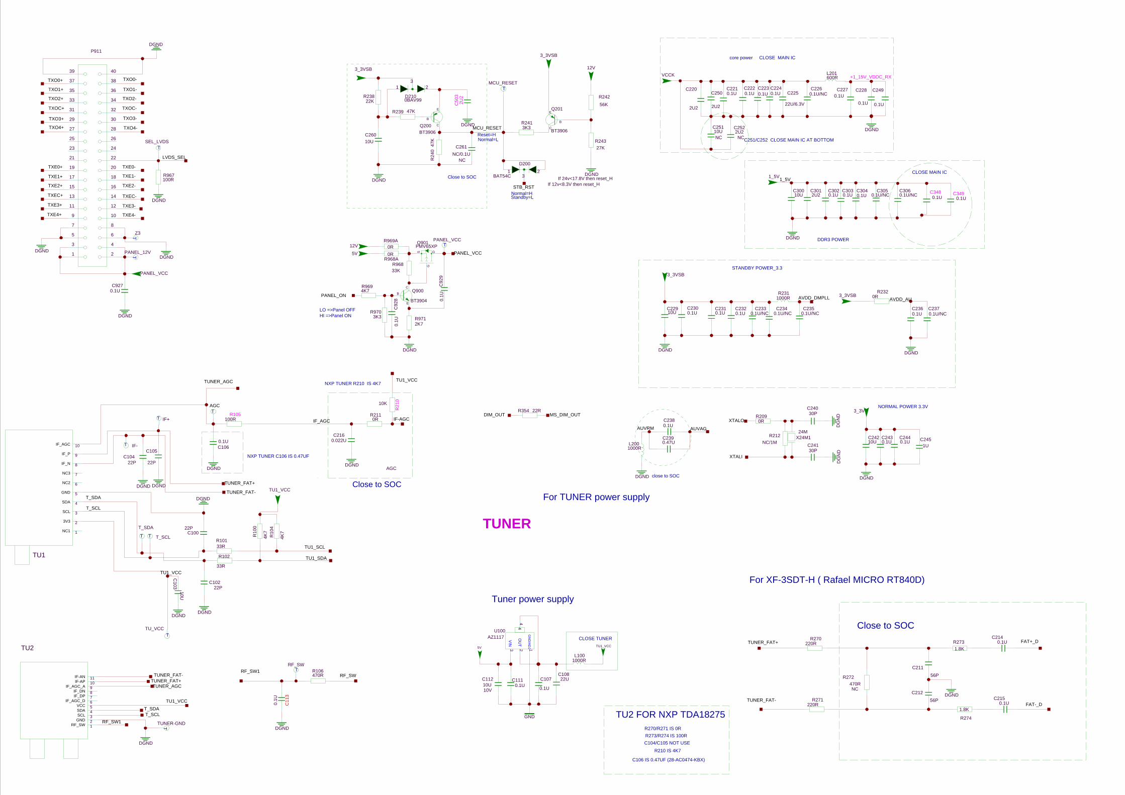
Signal of MS08BP/BPA/MS08GP Block Diagram
LVDS
TPA3110D Panel
LVDS Transimiter
POWERSUPPLY
12v in3.3vSTB in
1GDDR3 option For MS08GPDDR InterfaceLVDS InterfaceAudio R/L CH out
MSD6308RTEM/ MSD6308RTEMB
Nandflash,MS08BP /MS08GP 2G
MS08BPA 4G
Be in 2G DDR3SU
PCMCIA for MS08BP Nandflash date processor
DTV CC/CA Content protection
CICAM
MSD6308RTEM/ MSD6308RTEMB
Key/IR board
SPDIF
AV in CVBS+ Audio R/L
Key/IR controlVideo& sound signal processor
ATV&DTV Decoder
VGA
Audio R/L out
SPDIF
D+ / DRJ45 Network
MS08GP NXP TDA18275Antenna /Cable
ATV&DTV DecoderInternet connectivityHDMI TMDS
HD
HD
FAT+ / FAT-
U HD MS08BP/BPA Rafael RT840D
Antenna
RX+/RX-D+ / D-
W
RJ45 Network(ATV/DTV)
DM
I2
DM
I3
SB
DM
I1
Antenna(ATV/DTV)
WIFI

MS08BP/MS08GP+ POWER
BL_ON_OUT_ _
DIM PWM56V (40”)110V~
240V
LED
AMP1.5A/1.0A 5W*2/80%3 18A
12V
AMP
Panel/0.8APMK65XP0.8A/0.5A8W*2/85%
3.18AMAX:3.5A
5V MP2143 CORE 1.18V VCCK /1.8A
Panel on/offMPS1495/3A440MA/390
POWER_ON
3.3 STB/320MA/263MAUSB/500mA*1
MHL/500mA1.25A2.2A/1.7A
1.1A/0.9A
MPS1495/3A
TUNER TU1_VCC/180MA
WIFI/250mA
PMK65XP U100 LDO AS117-3V3SOT-223 TYPE
LDO AS1117-ADJ
1.2V_T2 DEMOD/165mA
1.5VDDR/500mA/120MA
3.3V NOR/390MA/100mA LDO AS1117-1.2VPOWER_ON
SOT-223 TYPE

T
DGND
DGND
DGND
DGND
DGND
AAM
IN
SWEN/SYNC
BST
FB
GND
VCC
DGND
DGNDDGND
DG
ND
DGND
DGND
DGND
AAM
IN
SWEN/SYNC
BST
FB
GND
VCC
T
T
T
T
OUT
AGND
FB
EN
PGND
SW
VIN
PG
T
T
GND/ADJ
OUT
VIN
4
DGND
DGND
DGND
DGND
DGND
DGNDDGND
DGND
DGND
DGNDDGND
DGND
DG
ND
DGND
GN
D/A
DJ
OU
T
VIN
4
DGND
T
T
...
DD-MM
DD-MM
DD-MM
DD-MM
...
...
...
...
...
... ...
...
...........
... ... ...
...
...
...
DD-MM-YY
...... OF :
PAGE:ON:BY:BY:
ON:
CHECKEDDATE
Last saved :DESCRIPTION Last modifNAME
A
3 2 1
F
E
D
C
B
8 7 6 5
5
4 3 2 1
TH
IS D
RA
WIN
G C
AN
NO
T B
E C
OM
MU
NIC
AT
ED
TO
UN
AU
TH
OR
IZE
D P
ER
SON
S C
OPI
ED
UN
LE
S S
PER
MIT
TE
D I
N W
RIT
ING
F
E
D
C
B
A
4678
FORMAT DIN A2
Index-LabDESIGNATION
SBU :
TCLNO:
DRAWN
NC
FOR DDR3 outside power supplyFor HbbTV USE
HI =>Panel ONLO =>Panel OFF
Shielding L 0710
Typ 3A
12V TO 5V
Shielding L 0710
5V NORMAL POWER
Typ 3A
For chip core power supply
Min 1.16V/ Max 1.24V
Vref=0.6V
(Vin=2.5V-5.5V)
@max3A
Fixed OCP=4.2A
Fixed Fsw=1.2MHZFor timing sequence
BOM COST=1.22RMB
If Vout=1.8V Set R015=150K R017=6.2K R016=68K
If Vout=1.5V Set R015=150K R017=8.2K R016=91K
If Vout=1V Set R015=150K R017=4.7K R016=220K
12V TO 3V3
3V3 POWER SUPPLY
For DDR3 power supply
For +1.2V T2 DEMOD power supply
VCC=0.8(39/12.33+1)=5.24V
VCC=0.8(39/7.27+1)=5.09V
FOR DDR3 power supply
Output 1.5076V=1.25*(1+68/330) & 200mA
If Vout=1.2V Set R015=150K R017=0R R016=150K
If Vout=1.18V Set R015=150K R017=120k R016=33K
C035
22U/6.3V
C01922U
Q0102N7002K
R0294K7NC
R02
84K
7N
C
R0450R
C03
910
U
R0271KNC
R02639K
NC
R01633K
1
40-MS08GP-MAA2HG
12-5-2014_10:07 7
GJZ
C010220U10V
470RR009
C044
22U/6.3V
100KR007
NC
5V
5V
R038
330R
12KR037
3_3V
C027 0.1U
C028 10U
Z3_3VSVB
3_3V
B
C
E
Q002
BT3904 0.1U
C02
4
POWER_ON
82KR008
POWER_ONR046
1K
R03633R
R01082K
+1_2V_DEMOD
R018510K
3_3V
1_5V
3_3VSB
3_3VSB
R015150K
5V
C008
10U/16V
NC
C009
10U/16V
10U
C011
4
3 2 1
AS1117AD
U004
C0020.01U
0.1U
/16V
C04
31
2
3
4
U006
LD1117S12
C02
610
U
120KR017
C017
0.1U
C0160.1U
R005220R
DIM_OUT
R00633K
1V5
R024330R
R02568R
VCCK
C01822U
C01510U
L0001UH VCCK
5
6
7
8
4
3
2
1
U001MP2143 C020
10U
R00
02K
2
BL_ON_OUT
R001330R
C0010.01UR003
10K
C0450.01U
DIM_PWM
BL_ON
POWER_ON
R004330R
POWER_ON_OUTPOWER_ON
BL_ONBL_ON_OUT3_
3VS
B
DIM_OUT DIM_PWM3_3VSB
VID0
Z+1_2V_DEMOD
C040
10U
3_3V
C041
0.1U
C0130.1U
1
2
36
5
8
4
7
U000 MP1495
C004NC/470P
L0016.8UH
R035
6K8
R011
10K
R013
0RR012
NC/10R
R034
33K
C005
1000P
C00315P
R01439K
0.1U
C012
C006
0.1U
0.1U
C007
12V
C029
10U/16V
NC
C030
10U/16V
10U
C036
C0380.1U
R03933R
1
2
36
5
8
4
7
U002 MP1495
C034NC/470P
L0026.8UH
R022
10K
R030
0RR020
NC/10R
R021
33K
R01982K
C0331000P
C04715P
R03139K
0.1U
C021
C032
0.1U
0.1U
C031 82KR033
100KR032
12V
R04033K
R0414K7
R0423K3 R043
2K7
G
DS
Q001PMV65XP
C02
50.
1U
3_3VSB
1_5V 1_5V_E
1_5V_E

WHITE
YELLOW
RED
DGND
DGND
DGND
DGND
T
T T
T
TT
T
T
T
T
T
TT
TT
TT
T
T
T
GND
R
L
DGNDDGND
DGND
DG
ND
DGND
DGND
DGNDDGND
DGND
DGND
DGND
DGND
DGND
DGND
T
close to conn. close to SOC
NEARLY IC
CLOSE TO SOC
close to Mstar IC
close to U300
ETHERNET WLAN CONNECTORIPTV IN
NEARLY CONNECTOR
VGA INPUT CIRCUIT
Must be differential 100ohmRJ45AV1 IN
Mini jack for AUDIO Output
Mini jack for AV Input
VGA_SDA
VGA_SCL
AV-VIN
AV-VIN
AV/YPBPR-LIN
AV/YPBPR-LIN
AV/YPBPR-RIN
AV/YPBPR-RIN
U0RX
U0TX
ZAV_VIN
VGA_VS_IN VGA_VS_IN
VGA_BLU_INVGA_BLU_IN
VGA_HS_INVGA_HS_IN
VGA_SOG_INVGA_SOG_IN
VGA_GRN_INVGA_GRN_IN
VGA_RED_INVGA_RED_IN
R24768R VCOM0
R25868R
75R
R99
0
AV-ROUT
4
1
2
3
P918
ZVGA-GND
VGA_RXD
R902A4K7
R903A
4K7
ZVGA-VS
ZVGA-HS
F922
C276 0.047U
C275 0.047U
C273 0.047U
C93
6
560P
100RR985
R982100R
VGA_GRN
C93
7
560P
VGA_RXD
R986100R
RXVN_1
RXVP_1
TXVN_0
TXVP_0
R920
75R
R918
75R
C9050.1U
C9070.1U
R919
75R
F901F900RXVN_1RXVP_1TXVN_0TXVP_0]
1
2
3
4
5
6
7
8 9
10
11
12
13
14
15
16
U900
TS8121CLF
75R
R917NET_TXC
NET_TX1P
NET_TX1N
NET_RX1P
NET_RX1N
NET_RXC
3
4
5
6
7
8
1
2
9
10
11
12
P902
RX1N
TXC
RX1P
TX1N
TX1P
RXCNET_RXC
NET_RX1N
NET_TXC
NET_RX1P
NET_TX1N
NET_TX1P
C916A1000P
R25733R
F91
9
F91
8
F91
7F
916
F91
5F
914
F91
3
F91
2
C274 0.047U
ZV
GA
-B
R25933R
R99
175
R
R98
975
R
10K
R98
8
R98
710
K
R256
33R
17
16
2
1
9
10
3
13
5
8
12
7
15
14
11
4
6
P917
ZVGA-RX
ZVGA-R
ZVGA-G
ZVGA-TX
F92
0
C941 100PNC
C940100P
NC
U0RX
U0TXR981100R
R984100R
R983 100R
VGA_TXD
VGA_BLU
VG
A_B
LU
VG
A_V
S
VG
A_R
XD
VG
A_G
RN
VG
A_H
S
VG
A_R
ED
VGA_VS
VGA_RED
VGA_HS
VG
A_S
DA
VG
A_S
CL
VG
A_T
XD
VGA_HS_IN
VGA_VS_IN
VGA_SCL
VGA_SDA
ZAVOUT-R ZAVOUT-LR254
220KC277
1000P
C939
2U2
C938
2U2
C278
1000P
R255
220K
ZAVOUT-GND
F923
AVOUT1_R_OUT
AVOUT1_L_OUT
F905
C935
NC/47P
R98
012
K
R24833R
C2650.047U
ZAV-RZAV-L
C271 2U2R977 10K
F906
F902R97475R
C272 2U2R978 10K
R97912K
AV/YPBPR_R_IN
AV/YPBPR_L_IN
AV1_V_IN
3_3VSB
VGA_TXD
ZAV1-GND1
AV-LOUT
C2640.047U
1
2
3
4
5
6P914

DGND
DGND
DGND
DGND
DGNDDGND
T
T
T
T
T
T
T
BLACK
T
T
T
T
TT
RX2+
GND1
RX2-
RX1+
GND2
RX1-
RX0+
GND3
RX0-
RXC+
GND4
RXC-
NC1
NC2
DDCCLK
DDCDA
GND5
VCC
HPD
RX2+
GND1
RX2-
RX1+
GND2
RX1-
RX0+
GND3
RX0-
RXC+
GND4
RXC-
NC1
NC2
DDCCLK
DDCDA
GND5
VCC
HPD
FAULTEN/EN#
GND
VIN
ILIM
VOUT
VIN
EN/EN# NC
GND
VOUT
DGND
DGNDDGND
DGNDDGND
DGND
DGND
DGND DGND
DGND
DGND
DGND
DGND
DG
ND
DGND
DGND
DGND
DGND
RX2+
GND1
RX2-
RX1+
GND2
RX1-
RX0+
GND3
RX0-
RXC+
GND4
RXC-
NC1
NC2
DDCCLK
DDCDA
GND5
VCC
HPD
T
VCC-1
DNEG-1
DPOS-1
GND-1
MNT-HOLE1
MNT-HOLE2
DGND
DGND
VGA UART R954/R955 NOT USE
GND
KEY1
NC
C198 CLOSE TO connect
NC
R-LED
GND
IR
3_3VSB
3_3VSB
close to SOC
SPDIF
WIF
I
USB CONNECTOR
HDMI/MHL
R244/C248 CLOSE TO IC
R904A
0R
NC
5V
C9210.1U
5V
USB1_D-_IN
USB1_D+_IN
D+D-
1
2
3
4
5
6
P907
C912100U10V
C906
100U10V 10U/16V
C917
USB_5V
15
16
2
5
8
11
17
19
13
14
7
9
4
6
1
3
10
12
18
P905
LED_OUT
C913
10U
C923100P
IR_IN
5V_USB
5V
3_3VSB
R9624K7
R961220R3_3VSB
3_3V
R90
1
220R
R900220R/NC
R964220R
5
4 3
2
1U902
RT9711A
F1
H1_SDA
H3_5V
H3_SDA
F3
H3_SCL
H2_5V
43
2
1
5
6U901
RT9728B
R9562R2
R94918K
R946NC/100R
R947 1K
MHL_EN
MHL_CABLE_DET
R948NC/10K
HDMI2_SDA
HDMI3_SCL
H3_RX2+
C910
10U
C919
0.1U
C911
0.1U
R9290R
R94210K
R941
4K7
C914
0.1U
H_CECH_CEC
H_CEC
H3_SDA
H3_HPD
H3_5V
H3_SCL
H3_HPD
H3_HPD_OUT B
C
E BT3904Q403
R9364K7
R934
10K
R9351K
R933 100R
R932 100RR931 47K
R930 47K
H3_5V
H3_SDA
H3_SCL
H3_RXC-
H3_RXC+
H3_RX0-
H3_RX1-
H3_RX1+
H3_RX2-
15
16
2
5
8
11
17
19
13
14
7
9
4
6
1
3
10
12
18
P904
AVDD5V_MHL
R94533RH2_HPD_OUT H2_HPD
C9262U2H1_ARC
R9271K
R925 100R
R924 100R
R921100R
R923 47K
R922 47K
H2_5VR9375R6
15
16
2
5
8
11
17
19
13
14
7
9
4
6
1
3
10
12
18
P903
H1_HPD
H1_RXC-
H1_RXC+
H1_RX0-
H1_RX0+
H1_RX1-
H1_RX1+
H1_RX2-
H1_RX2+
H_CEC
H_CECCEC
F403
C918
0.047U
R939
300K
R938100R MHL_CABLE_DETMHL_DETECT
H2_5VR944 100R
R943 100R
H2_RX2+
H2_RX0+
H2_RX1-
H2_RX2-
H2_RX1+
H2_RX0-
H2_RXC+
H2_RXC-
MHL_DETECT
H1_HPD
H1_SCL
H_CEC
H1_5VF2
H2_SDA
H2_SCL
H2_HPD H2_HPD
H1_HPD
H1_5V
H1_SDA
H1_SCL
H1_SCL
H1_HPD_OUT
HDMI1_SDAHDMI1_SCL
H1_SDA
B
C
E BT3904Q402
R9284K7
R926
10K
H1_ARC_OUT
H1_ARC
H2_5V
H2_SDA
H2_SCL
HDMI2_SCL
H2_SCL
H2_SDA
H1_5V
H3_HPD
H3_RX0+
H_CEC
HDMI3_SDA
H2_5V5V
US
B2_
D+
US
B2_
D-
1
2
3
4
5
6
P908
WIFI_ON
C92
00.
1U
R965 2R2
R966 2R2
R9510R/1206/NC
R9504K7
C91510U
R957
2R2
USB1_D-
GND
USB1_D+
1
2
P912R963120R
C931
33P
C9300.1U
SPDIF
Z1SPDIF_OUT
R95847K
IR
1
2
3
4
5
P910
1
2
3
4
P909R960
1K
3_3VSB
0.1UC248
R24422K
LED
0.1U
C925
0.1U
C924
KEY
13
2
D100 0BAV99NC/
F103
Z2
KEY_IN
3_3VSB
KEY_IN
LED_OUT
KEY
WIFI_EN
C9542P2NC
C9532P2NC
USB2_D-
USB2_D+
GND
GN
D/A
DJ
OU
T
VIN
4
DGND
DGND
T
T T
T
T
T
T
TT
T
IF_AGC
NC2
NC3
IF_N
NC1
SCL
3V3
SDA
GND
IF_P
DGND
DGND
DGND
DGND
DGND
DGND
DGNDDGND
DGND
DGND
DGND
DGND DGND
DG
ND
DG
ND
DGND
DGNDDGND
DGND
DGND
DGND
DGND
DGND
DGND
T
T
IF_AGC_D
IF-ANIF-AP
IF_DPIF_DN
RF_SW
SCLGND
SDAVCC
IF_AGC_A
T
DGND
TU2 FOR NXP TDA18275
For TUNER power supplyClose to SOC
close to SOC
If 24v<17.8V then reset_HIf 12v<8.3V then reset_H
Standby=LNormal=H
Normal=LReset=H
Close to SOC
HI =>Panel ONLO =>Panel OFF
NORMAL POWER 3.3V
STANDBY POWER_3.3
DDR3 POWER
NXP TUNER R210 IS 4K7
Close to SOC
TUNER
Tuner power supply
core power CLOSE MAIN IC
CLOSE MAIN IC
C251/C252 CLOSE MAIN IC AT BOTTOM
For XF-3SDT-H ( Rafael MICRO RT840D)
NXP TUNER C106 IS 0.47UF
R270/R271 IS 0R
R273/R274 IS 100R
C104/C105 NOT USE
R210 IS 4K7
C106 IS 0.47UF (28-AC0474-KBX)
CLOSE TUNER
X24M124M
TU1_VCC
TU1_VCC
C10822U
C1060.1U
TUNER_AGC
TUNER_FAT-
TUNER_FAT+
C211
56P
TUNER_AGC
TUNER_FAT-
AGC
AGC
TUNER_FAT+
6
1110
78
1
32
45
9
TU2
T_SCLT_SDA
TUNER-GND
RF_SW
RF_SW1
RF_SW1
C3490.1U
C3480.1U
C2522U2NC
C25110UNC
C3012U2
C30010U
VCCK
C250
2U2
C220
2U2
+1_15V_VDDC_RX
C249
0.1U
C225
22U/6.3V
C228
0.1U
L1001000R
R2311000R
R969A0R
0.1U
C92
9
R2731.8K
R274
1.8K
R271220R
C212
56P
R270220R
R272470RNC
C2140.1U
C2150.1U
R21
010K
C24130P
C24030P
FAT-_D
10
6
7
8
1
3
2
4
5
9
TU1
T_SDA
T_SCL
TU1_VCC
TU1_VCC
IF+
C10222P
TUNER_FAT-
B
E
C
BT3906Q200
B
E
CBT3906
Q201
L201600R
B
C
E
Q900
BT3904
1 23
D200
BAT54C
MCU_RESET
C50
32U
2
C26010U
3_3VSB
1_5V1_5V
C2330.1U/NC
C2310.1U
3_3V
3_3VSB
R2320R
C2451U
AVDD_DMPLL AVDD_AU
C2220.1U
C2260.1U/NC
C2270.1U
C2210.1U
C2230.1U
C2240.1U
C3020.1U
C3030.1U
C3040.1U
C3060.1U/NC
C3050.1U/NC
C2300.1U
C2320.1U
C2340.1U/NC
C2360.1U
C2370.1U/NC
C2350.1U/NC
C22910U
C2430.1U
C2440.1U
C24210U
C9270.1U
Z3
PANEL_12V
PANEL_VCC
R354 22R
R96833K
R9694K7
R9703K3 R971
2K7
13
2
0BAV99D210
G
DS
Q901PMV65XP
C92
80.
1U
PANEL_VCC
R239 47K
47K
R24
0
R2413K3
12V
3_3VSB
MCU_RESET
56K
R242
R24327K
5V
12V
C261
NC/0.1UNC
R23822K
3_3VSB
1 2
4
6
8
12
14
16
18
20
10
22
24
26
28
3
5
7
9
11
13
15
17
19
21
23
25
27
29 30
32
34
36
38
40
31
33
35
37
39
P911
R967100R
SEL_LVDS
LVDS_SEL
TXE3-
TXEC-
TXE2-
TXE1-
TXE4-
TXO4-
TXE3+
TXEC+
TXE2+
TXO4+
TXO3+ TXO3-
TXOC-
TXO2-
TXO1-
TXO0-
TXOC+
TXO2+
TXO1+
TXO0+
DIM_OUT
PANEL_VCC
STB_RST
MS_DIM_OUT
PANEL_ON
TXE0+ TXE0-
TXE1+
TXE4+
XTALOC2380.1U
C2390.47U
AUVRM AUVAG
R212NC/1M
0RR209
L2001000R
R105100R
R2110R
R102
33R
C2160.022U
TU_VCC
T_SCL
C103
10U
R10
4
4K7
R10
0
4K7
R10133R
C10022P
C105
22PC104
22P
T_SDA
IF-
TU1_SCL
TU1_SDA
TUNER_FAT+
IF-AGCIF_AGC
FAT+_D
R968A0R
123
4
U100AZ1117
5V
0.1U
C107C1110.1U
C11210U10V
R106470R
C11
3
0.1U
RF_SW
TU1_VCC
XTALI

DGND
VIFPVIFM
IFAGC
TGPIO0
T_I2C_CLKT_I2C_SDA
PCM_D0PCM_D1PCM_D2PCM_D3PCM_D4PCM_D5PCM_D6PCM_D7
PCM_A0PCM_A1PCM_A2PCM_A3PCM_A4PCM_A5PCM_A6
PCM_WAIT_N
PCM_A8PCM_A9
PCM_IOWR_N
PCM_A11
PCM_A7
PCM_A12
PCM_RESETPCM_IRQA_N
PCM_OE_NPCM_IORD_N
PCM_A10
PCM_CE_NPCM_WE_N
PCM_A14
PCM_CD_N
PCM_A13
PCM_REG_N
NAND_ALENAND_WPZNAND_CEZNAND_CLENAND_REZNAND_WEZNAND_RBZ
TGPIO1
TS0_D0TS0_D1TS0_D2TS0_D3TS0_D4TS0_D5TS0_D6TS0_D7
TS0_CLKTS0_VLD
TS0_SYNC
TS1_D0TS1_D1TS1_D2TS1_D3TS1_D4TS1_D5TS1_D6TS1_D7
TS1_CLKTS1_VLD
TS1_SYNC
LINE_OUT_0LLINE_OUT_0R
LINE_IN_1LLINE_IN_1RLINE_IN_2LLINE_IN_2R
VAGVRM
SPDIF_INSPDIF_OUT
I2S_OUT_MCKI2S_OUT_WS
CEC
I2S_OUT_BCK
I2S_OUT_SD
IRIN
RESET
XTALINXTALOUT
TESTPIN
PAD_ARC0
LINE_IN_3LLINE_IN_3R
I2S_IN_WS/T2_RESETI2S_IN_BCK/T2_I2CS_SCLI2S_IN_SD/T2_I2CS_SDA
MHL_VBUS_ENMHL_CABLE_DETMCP_TEST
SPI1_DISPI1_CKSPI2_DISPI2_CK
EARPHONEOUTREARPHONEOUTL
C_RX0NC_RX0PC_RX1NC_RX1PC_RX2NC_RX2PC_RXCNC_RXCP
DDCDC_CKDDCDC_DAHOTPLUGC
D_RX0ND_RX0PD_RX1ND_RX1PD_RX2ND_RX2PD_RXCND_RXCP
DDCDD_CKDDCDD_DAHOTPLUGD
A_RX0NA_RX0PA_RX1NA_RX1PA_RX2NA_RX2PA_RXCNA_RXCP
DDCDA_CKDDCDA_DAHOTPLUGA
SPDIFMHL
demod
I2S
HDMI
Analog audioKEY0LED_RARC_DET
3D_EN/PCM_PWR_ENAMP_MUTEBRI_ADJ
PM_SPI_CKPM_SPI_DIPM_SPI_DO
UART0_RXUART0_TX
M_I2C_SLCM_I2C_SDA
PWM_PM
LDELCK
LVSYNCLHSYNC
UART_RX2UART_TX2
SAR3
VID0PANNEL_ON/OFFPWR_ON/OFFVBL_CTRLPMCONFIG03D_LR_INPMCONFIG1
TCON0TCON1TCON2TCON3TCON4TCON5TCON6TCON7
LVA0NLVA0PLVA1NLVA1PLVA2NLVA2P
LVACKNLVACKP
LVA3NLVA3PLVA4NLVA4P
LVB0NLVB0PLVB1NLVB1PLVB2NLVB2P
LVBCKNLVBCKP
LVB3NLVB3PLVB4NLVB4P
PM_SPI_CZ1N
SAR
PWM
SPILVDS
TCONGPIO_PM
DG
ND
DGND
DGND
DGNDDGND
DG
ND
GIN0PGIN0M
HSYNC0VSYNC0
GIN1P
SOGIN1
CVBS0PCVBS1P
VCOM0
TP
RN
TNRP
DM_P0DP_P0DM_P1DP_P1
RIN0P
BIN0P
RIN1PGIN1M
BIN1P
CVBS_OUT
RIN2PGIN2MGIN2PBIN2P
VSYNC2HSYNC2
RGB USB
CVBS
PHYVDDC1VDDC2VDDC3VDDC4VDDC5VDDC6
AVDDL_MOD
DVDD_RX_1
DVDD_RX_1_1
DVDD_RX_2
DVDD_RX_2_1
DVDD_DDR
DVDD_NODIE
AVDD_DDR0_DAVDD_DDR0_D1AVDD_DDR0_D2AVDD_DDR0_CMD
AVDD_DDR1_DAVDD_DDR1_D1AVDD_DDR1_D2AVDD_DDR1_CMDAVDD_DDR1_CLK
AVDD_NODIE
AVDD_DVI_USB_MPLLAVDD_DVI_USB_MPLL1
AVDD_AU33
AVDD3P3_DMPLL
VDDP
AVDD_MODAVDD_MOD1
AVDD_PLL
AVDD_DRAMAVDD_DRAM1
GND_EFUSE
AVDD5V_MHL
GNDGND1GND2GND3GND4GND5GND6GND7GND8
GND9
GND10GND11GND12GND13
GND14GND15GND16GND17GND18GND19
GND20GND21GND22GND23GND24GND25GND26GND27GND28GND29
GND30GND31GND32
GND33
GND34
GND35GND36GND37GND38GND39GND40GND41GND42GND43GND44GND45GND46GND47GND48GND49GND50GND51GND52GND53GND54
GND55GND56GND57GND58GND59
GND60GND61GND62GND63GND64GND65GND66GND67GND68GND69
GND70GND71GND72GND73GND74GND75
DVDD_DDR1
GND76
VDDC7
MCP_VDDCMCP_VDDC1
GND77
GND78
GND79GND80
GND81
GND82GND83GND84
VDDC
DG
ND
T
PCMCIA PIN
PCMCIA PIN
H
LEVEL
PM_CONFIG1
close to SOC
PM_CONFIG0
LG_DIM_OUT
SPI_SDI
Chip config
Chip config PIN
H
L
H
PCMCIA PIN
PCMCIA PIN
PCMCIA PIN
TO NANDFLASH
CLOSE TO MAIN IC
C2534U7
PCM_A7PCM_A6
RF_SW
LG_DIM_OUT
PM_CONFIG1
SPI_SDI
PM_CONFIG0
ZCVBS_OUT
C2900.1U
N12N13N14N15P12P13
P14
M12
A7
M14
B7
M13
F8
C5K12L12K11
C6K14L14K13L13
J7
K7L7
R6
R5
R15
R16R17
R18
B5B6
H7
V6
A13A15A18B12B14B16B17B19B20
A6
C9C10C21
D9
F11F13F15F17F19F21
G9G10G11G12G13G14G15G16G17G18
H8H9
H10
K10
L10
M7M8M9M10N4N5N6N7N8N9N10P4P5P6P7P10P15P16P17P18
R7R11R12R13R14
H17H18J8J9J10J11J12J13J14K8
H11H12H13H14H15H16
C7
E20
M11
N11P11
G8
K9
L8L9
R4
T6T7U6
L11
U200
MSD6308RTMN
L3L2
M5M4
N3
M1
T3T1
T2
C1
B2
C2B1
C4B4Y10W10
M3
K2
N2N1
M2
R1
R2R3P2P3
M6K4
U200
MSD6308RTMN
WIFI_EN
F4D4G7
T18T17U18
D6E7D7
L5L4
L15K15
K5
G20H19G21G19
L16L17
G5
W3E8D1D8U3D5G6
J16J17J15K17J18K18K16L18
N19N21N20P19P20R19R20R21T19T21T20U19
H20J19J20J21K19K21K20L19L20M19M20M21
F7
U200
MSD6308RTMN
PCMCIA_VCC_EN
V2V1
U5V5T5T4
V3U2
E6A4
B3C3
J6
A3
A2
F6
D3
AA2AA3
F9
J5
V4U4
E4F5E5
W5AA10P8
P9R8R9
R10
Y5W4
W7Y8W8Y9AA9W9AA7Y7W6AA6Y6
E2F3F2F1G3G1D2E3J4L6K6
H2J3J2J1K3K1G2H3H6H5G4
U200
MSD6308RTMN
HP_L
HP_R
AV/YPBPR_R_IN
W2W1
Y3
AA4
Y2Y1
U20V15
AA18Y20T16
W18T14Y21
Y18W17Y17W16Y16
AA16W15
V21
Y19AA19
U17
W21
AA15
V20
W19U16
T15V16
AA20
U15U14
V17
V19
W20
V18
T8T9V7U9V9U8U7
Y4
W14W13W11Y15Y13Y12Y14W12AA12AA13Y11
T13U13T12U10T11U11T10V12V13U12V10
U200
MSD6308RTMN
PCM_A2PCM_A1PCM_A0
VGA_VS_INVGA_HS_IN
VGA_BLU_IN
VGA_GRN_INVGA_SOG_IN
VGA_RED_IN
HP_DET_IN
AVOUT1_R_OUT
3_3VSB
R218 4K7NC/
C247
33PNC/
R220 4K7NC/
R217 4K7
R216 4K7
R215 4K7NC/
R214 4K7NC/
C246
1U
R213 4K7
R219 4K7
3_3VSB
AMP_MUTE
LG_DIM_OUT
TXO0+TXO0-
+1_15V_VDDC_RX
VCCK
SPI_SDI
STB_RSTPM_CONFIG1
PM_CONFIG0
VID0
AVDD_DMPLL
AVDD_AU
3_3V
AVDD5V_MHL
1_5V
HDMI3_SDAHDMI3_SCL
H3_HPD_OUT
H3_RXC+H3_RXC-H3_RX2+H3_RX2-H3_RX1+H3_RX1-H3_RX0+H3_RX0-
H2_RX0-
HDMI2_SDAHDMI2_SCL
H2_HPD_OUT
H2_RXC+H2_RXC-H2_RX2+H2_RX2-H2_RX1+H2_RX1-H2_RX0+
HDMI1_SDAHDMI1_SCL
H1_HPD_OUT
H1_RXC+H1_RXC-H1_RX2+H1_RX2-H1_RX1+H1_RX1-H1_RX0+H1_RX0-
CECH1_ARC_OUT
SPDIF_OUT
MHL_ENMHL_CABLE_DET
XTALOXTALI
MCU_RESET
IR_IN
AUVRMAUVAG
AVOUT1_L_OUT
AV/YPBPR_L_IN
TXOC+TXOC-
TXO4+
TXO3+TXO3-
TXO2+
TXO1+
TXO4-
TXO2-
TXO1-
TXE3-
TXE2-
TXEC+TXEC-
TXE4+
TXE3+
TXE2+
TXE1+
TXE0+TXE0-
TXE4-
TXE1-
POWER_ON_OUTBL_ON_OUT
PANEL_ON
U0TXU0RX
LED_OUTKEY_IN
MS_DIM_OUT
PCM_A4PCM_A5
PCM_A3
NAND_RBZNAND_WEZNAND_REZNAND_CLENAND_CEZNAND_WPZNAND_ALE
TU1_SDATU1_SCL
IF-AGC
FAT-_DFAT+_DVCOM0
AV1_V_IN
USB1_D+_INUSB1_D-_INUSB2_D+USB2_D-
TXVP_0
RXVP_1RXVN_1
HD1_SOG_INHD1_PB_INHD1_Y_INHD1_Y_IN-HD1_PR_IN
TXVN_0
C289
0.1U
CVBS_OUT
+1_2V_DEMOD

DGND
DGND
DGND
A0A1A2A3A4A5A6A7A8A9A10A11A12
DQU0DQU1DQU2DQU3DQU4DQU5DQU6DQU7
DQSU/DQSU
DMU
DQL0DQL1DQL2DQL3DQL4DQL5DQL6DQL7
DQSL/DQSL
DMLBA0BA1BA2
/CS/RAS/CAS/WE
CK/CK
CKE
ODT
/RESET
VREFCA
VREFDQ
ZQ
VD
DQ
VD
DQ
1
VD
DQ
2V
DD
Q3
VD
DQ
4V
DD
Q5
VD
DQ
6V
DD
Q7
VD
DQ
8
VS
SQ
VS
SQ
1
VS
SQ
2V
SS
Q3
VS
SQ
4V
SS
Q5
VS
SQ
6V
SS
Q7
VS
SQ
8
VD
DV
DD
1V
DD
2V
DD
3V
DD
4V
DD
5V
DD
6V
DD
7V
DD
8
VS
SV
SS
1V
SS
2V
SS
3V
SS
4V
SS
5V
SS
6V
SS
7V
SS
8V
SS
9V
SS
10
NC1NC2NC3NC4NC5NC6NC7
VS
S11
NC/RSTNCNC1NC2NC3R/B2R/B1RECE1CE2NC4VCCVSSNC5NC6CLEALEWEWPNC7NC8NC9NC10NC11 NC12
NC13NC14NC15
I/O0I/O1I/O2I/O3
NC16NC17NC18VSS1VCC1
PRENC19NC20
I/O4I/O5I/O6I/O7
NC21NC22NC23NC24
DGND
DGND
DG
ND
DGND DGND
DGND
DG
ND
ZQ
B_A[0]B_A[1]B_A[2]B_A[3]B_A[4]B_A[5]B_A[6]B_A[7]B_A[8]B_A[9]
B_A[10]B_A[11]B_A[12]B_A[13]B_A[14]
B_DQL[0]B_DQL[1]B_DQL[2]B_DQL[3]B_DQL[4]B_DQL[5]B_DQL[6]B_DQL[7]B_DQU[0]B_DQU[1]B_DQU[2]B_DQU[3]B_DQU[4]B_DQU[5]B_DQU[6]B_DQU[7]
B_CASZB_RASZB_WEZ
B_DQMLB_DQMU
B_ODTB_BA[0]B_BA[1]B_BA[2]B_RSTB_CKE
B_MCLKB_MCLKZ
B_DQSLB_DQSLBB_DQSU
B_DQSUBB_CS0
MIU1MIU0
DGND
DGND
DGND
Close to DDR POWER PIN
1G DDR3 For HbbTV USE
E9
E11F12D10B10E15B11F14C11D14A12F16D13D15C12E13A20A16C19C15C20C14B21B15F18D19D17E21E19D20D18F20B9C8D11C16D21B8A9D16A10F10E17C13B13A19C18B18C17D12
U200
MSD6308RTMN
C34
7
0.1U
C33
0
0.1U
C33
3
0.1U
C33
2
0.1U
C33
1
0.1U
0.1U
C33
5
0.1U
C33
6
0.1U
C33
7
0.1U
C33
8N
C/
0.1U
C33
9
0.1U
C32
9
123456789
101112131415161718192021222324 25
2627282930313233343536373839404142434445464748
U301MT29F4G08AB
R323 22R
R321 22R
R319 22R
R320 22R
PCM_A7
PCM_A4
PCM_A3
N3P7P3N2P8P2R8R2T8R3L7R7N7
D7C3C8C2A7A2B8A3
C7B7
D3
E3F7F2F8H3H8G2H7
F3G3
E7M2N8M3
L2J3K3L3
J7K7K9
K1
T2
M8
H1
L8
A1
A8
C1
C9
D2
E9
F1
H2
H9
B9
B1
D1
D8
E2
E8
F9
G1
G9
B2
D9
G7
K2
K8
N1
N9
R1
R9
A9
E1
G8J2J8M1
M9
P1
P9
T1
T9
J1J9L1L9M7T3T7
B3
U300
NT5CB64M16C
345
1000P
C344
0.1U
C343
0.1U
C342
1000P
R352
PART_TYPE=RE-0402
22R
OUTLINE=0402
5 4
7 2
1
36
8
R351
22R
R34122R
5 4
7 2
1
36
8
R342
22R
5 4
7 2
1
36
8
R340
22R
5 4
7 2
1
36
8
R338
22R
5 4
7 2
1
36
8
R336
22R
5 4
7 2
1
36
8
R334
22R
5 4
7 2
1
36
8
R332
22R
5 4
7 2
1
36
8
R331
22R
5 4
7 2
1
36
8
R330
22R
5 4
7 2
1
36
8
R329
22R
R30
156
RC
340
0.01
U
5 4
7 2
1
36
8
22R
R328
5 4
7 2
1
36
8
R327
22R
R23
0
240R
1_5V_E
1_5V_E
C33
4
2U2
C34
6
2U2
R3061K
R3051K
R3041K
R35
356
R
R300240R
R35022R
1_5V_E
R3071K
1_5V_E
5 4
7 2
1
36
8
R333
22R
5 4
7 2
1
36
8
R335
22R
5 4
7 2
1
36
8
R337
22R
5 4
7 2
1
36
8
R339
22R
5 4
7 2
1
36
8
R343
22R
5 4
7 2
1
36
8
R344
22R
5 4
7 2
1
36
8
R345
22R
5 4
7 2
1
36
8
R346
22R
5 4
7 2
1
36
8
R347
22R
5 4
7 2
1
36
8
R348
22R
5 4
7 2
1
36
8
R349
22R
B-DDR3-DQU5
B-DDR3-BA2
B_DDR3_CS0
B_DDR3_DQSUB
B_DDR3_DQSLB
B_DDR3_DQSUBB_DDR3_DQSUB_DDR3_DQSLBB_DDR3_DQSLB_DDR3_MCLKZB_DDR3_MCLKB_DDR3_CKEB_DDR3_RESET
B_DDR3_BA2
B_DDR3_BA2B_DDR3_BA1B_DDR3_BA0B_DDR3_ODTB_DDR3_DMUB_DDR3_DMLB_DDR3_WEZB_DDR3_RASZB_DDR3_CASZ
B_DDR3_DQU6
B_DDR3_DQU4
B_DDR3_DQU0
B_DDR3_DQU7B_DDR3_DQU6B_DDR3_DQU5B_DDR3_DQU4B_DDR3_DQU3B_DDR3_DQU2B_DDR3_DQU1
B_DDR3_DQL7
B_DDR3_DQL7B_DDR3_DQL6B_DDR3_DQL5B_DDR3_DQL4B_DDR3_DQL3B_DDR3_DQL2B_DDR3_DQL1B_DDR3_DQL0
B_DDR3_A3
B_DDR3_A0
B_DDR3_A7
B_DDR3_A13
B_DDR3_A9
B_DDR3_A14B_DDR3_A13B_DDR3_A12B_DDR3_A11B_DDR3_A10B_DDR3_A9B_DDR3_A8B_DDR3_A7B_DDR3_A6B_DDR3_A5
B_DDR3_A3B_DDR3_A2B_DDR3_A1B_DDR3_A0
B-MVREFDQ
B-DDR3-MCLKZ
B_DDR3_RESET B-DDR3-RESET
B_DDR3_DQU5
B_DDR3_DML B-DDR3-DML
B-DDR3-DQL2
B-DDR3-DQL0
B-DDR3-DQU7
B-DDR3-DQU6
B-DDR3-DQU2
B-DDR3-WEZ
B-DDR3-CASZ
B-DDR3-CS0
B-DDR3-BA2
B-DDR3-A7
B-DDR3-A8
B-DDR3-A11
B-DDR3-A12
B-DDR3-A3
B-DDR3-A9
B-DDR3-A13
B_DDR3_BA0
B_DDR3_CASZ
B-DDR3-BA0
B_DDR3_A2
B-DDR3-A0
B-DDR3-A2
B_DDR3_A5 B-DDR3-A5
B_DDR3_WEZ
B_DDR3_CS0
B-DDR3-RASZ
B-DDR3-ODT
B_DDR3_RASZ
B_DDR3_ODT
B_DDR3_A11
B_DDR3_A8
B_DDR3_A6
B_DDR3_A4
B-DDR3-A6
B-DDR3-A4
B_DDR3_BA1
B_DDR3_A12
B-DDR3-BA1
B_DDR3_DQU0 B-DDR3-DQU0
B-DDR3-DQU4
B_DDR3_MCLK
B_DDR3_MCLKZ
B-DDR3-MCLK
B_DDR3_DQL1
B_DDR3_DQL3
B-DDR3-DQL1
B-DDR3-DQL3
B_DDR3_DQL5
B-DDR3-DQL7
B-DDR3-DQL5
B_DDR3_DQU2
B-DDR3-DQSUB
B-DDR3-DQSUB_DDR3_DQSU
B-DDR3-DQSLB
B-DDR3-DQSLB_DDR3_DQSL
B_DDR3_DQU3
B_DDR3_DMU
B-DDR3-DQU3
B-DDR3-DMU
B_DDR3_DQU7
B_DDR3_DQU1 B-DDR3-DQU1
B-DDR3-DQL6
B-DDR3-DQL4
B_DDR3_DQL6
B_DDR3_DQL4
B_DDR3_DQL2
B_DDR3_DQL0
B-MVREFCA
B-DDR3-MCLKB-DDR3-MCLKZ
B-DDR3-A0
B-DDR3-A2B-DDR3-A1
B-DDR3-A3B-DDR3-A4B-DDR3-A5B-DDR3-A6B-DDR3-A7B-DDR3-A8B-DDR3-A9B-DDR3-A10B-DDR3-A11B-DDR3-A12
B-DDR3-BA0B-DDR3-BA1
B-DDR3-CS0
B-DDR3-CASZB-DDR3-RASZ
B-DDR3-WEZB-DDR3-ODT
B-MVREFCA
B-DDR3-A13B-DDR3-A14
B-DDR3-DQSUBB-DDR3-DQSUB-DDR3-DMU
B-DDR3-DQU0B-DDR3-DQU1B-DDR3-DQU2B-DDR3-DQU3B-DDR3-DQU4B-DDR3-DQU5B-DDR3-DQU6B-DDR3-DQU7
B-DDR3-DMLB-DDR3-DQSLB-DDR3-DQSLB
B-DDR3-DQL0B-DDR3-DQL1B-DDR3-DQL2B-DDR3-DQL3B-DDR3-DQL4B-DDR3-DQL5B-DDR3-DQL6B-DDR3-DQL7
B-DDR3-CKEB-DDR3-RESET
B-MVREFDQ
B_DDR3_A4
B-DDR3-A10
B-DDR3-CKEB_DDR3_CKE
B_DDR3_A10
B-DDR3-A1
B-DDR3-A14B_DDR3_A14
B_DDR3_A1
C32433P
C32533P
R326NC/10K
R32
510
K
NC/0RR324
R311 22R
R309 22R
3_3V
3_3V
C3200.1U
2U2C321
C32
20.
1U
C32
30.
1U
R322 22R
R318 22R
R317 22R
R316 22R
R315 22R
R314 22R
R313 22R
R312 22R
R310 22R
NAND_CLE
NAND_ALE
NAND-D1NAND-D0
NAND_REZ
NAND-RBZ
PCM_A5
NAND-D1
PCM_A6
NAND-D5
NAND-D6
NAND-D7
NAND-D7 NAND_RBZ
NAND_WPZ
NAND_WEZ
NAND_CEZ
NAND-REZ
NAND-WEZNAND-ALENAND-WEZ NAND-WPZ
NAND-ALE
NAND-CLE
NAND-CLE
NAND-CEZNAND-CEZ
NAND-RBZNAND-REZ
NAND-D5NAND-D4
NAND-D3NAND-D2
NAND-D6
PCM_A0
PCM_A1
PCM_A2
NAND-D0
NAND-D2
NAND-D3
NAND-D4
NAND-WPZ

DGND
DG
ND
DGND
DGND
T
TT
T T
DGND
DGNDDGND
DGND
DGND
DGND
DGNDDG
ND
PVCCL1
NC
PBTL
OUTPL
BSPL
PVCCR1
PVCCR2
LINP
LINN
GAIN0
GAIN1
AVCC
AGND
BSPR
OUTPR
PGND1
OUTNR
BSNR
OUTNL
PGND2
BSNL
GVDD
PLIMIT
RINN
RINP
PVCCL2SD
FAULT
DGND
DGND
DGND
DGND
DGND
DGND
DG
ND
DGND
GAINGAIN020dB26dB32dB36dB
LH
HH
L
HL
GAIN1
Power AMP TPA3113D2
close to SOC
L
R+
R-
L-
L+
RED
WHITE
MUTE Circuit
CLOSE AMP IC
CLOSE AMP IC
2
1
P600
2
1
P601
OUTLN
OUTLN
OUTLP
OUTLP
OUTRNOUTRP
OUTRP
C6410.1U
12VA
AMP_L
R61210R
R60610K
AMP_MUTE
R60
54K
7N
C
C6041000P
C624
330P
27
13
14
25
26
15
16
1
2
3
4
5
6
7
8
17
18
19
20
21
23
24
22
9
10
11
12
28
U600
TPA3113D2
C616330P
R61710R
C613
330P
C600
220U16V
HP_R
HP_L
C6220.1U/50V
C6140.1U/50V
1U/50VC636
HP_R
HP_L
C6170.1U/50V
12VA
AMP_R
OUTLPOUTLN
OUTRN OUTRP
L600392170
C629 1U
C628 1U
12VA
12V
0RR634
R63110K
GAIN1
GAIN0
R62210R1UC602
1UC608
1UC607
C6120.22U
R62810R
R611100R L602
220R/NC
R61310K
C6260.1U
C6110.1U
C6251000P
C6101000P
L60622UH
L60322UH
L60122UH
L60822UH
C621 0.1U/50VC620
330P
R629100K
C6091000P
1UC606
R615100R
R61410K
1UC605
1UC603
1KR610
L607220R/NC
L605220R/NC
L604
220R/NC
C623
0.22U
C619
0.22U
C6180.22U
R61610R
OUTRN
OUTLN
OUTRP
OUTLP
SD
R6201K
R6351K
6.8NC631 R621
NC/100K
R636
NC/100K
6.8NC630
NC/0RR633
R632NC/10K
3_3VSB
GAIN1GAIN0
OUTRN
R60
44K
7
R60
94K
7
B
C
E
Q602BT3904
MUTE
3_3VSB
3_3VSB
SD
C6420.1U

!
PGND
!
!
!
! !
!!
GND
GND
PGND
PGND
GND
GN
D
GND
GND
GND
GND
GND
GN
D
PGND
PGND
GND
PG
ND
GND
GND
PGND
GN
D
GND
T
!
VAL?
VAL?
GND
T
T
TT
T
GN
D
PGND
T
GND
PGND
PGND
PG
ND
VDD
FSW
COMP
GND1
ISET
PWMI
EN
FB4 FB3
FB2
FB1
OVP
GND2
CS
GATE
VCC
V
N3
N1
N4
N2
E1,E2
GATE
CS
VDD
RT
FB
GND
T
!
!
!
T
T
T
T
T
T
T
! !
!
T
T
T
T
T !
!
!
T
SCH
SCH V 1.0
2.5V
/2K
=1.
25m
A
LED Driver
MS08FP
MS08FP.SCH
+50VLEDNCR838
ZPC1
R8331K
FR207 D801
D802FR104
2
43
1
L81
F81
3.15A250VAC
ZL
ZN
ZPGND
12C
N80
0
12V
Z50V
ZPCGND
R83
1M2
R81
1M2
R84 1M
2
R82
1M2
NTC81
1R5
ZVCC1
ZHV
GND
12V
12V-1
GND-1
1
23
4
PC820
TLP781
ZPC2
ZFB
1R5
NTC82
0.47
UC
X81
231
D850A
MBR10150
6
4
5
3
2
1
U801
RT7736
43
2
1
L82
VCC1
2
4
1
3
5
12
11
10
9
8
76
T801
D850
MUR460R85033R
231
D830MBR10150
VR81680V
13
8
15
3
6
16
9
5 4
2
1
7
14
10
11
12
U770
GB98A
FSW
VCCR779A
100K
R779B
NC
LED3
LED4
C77
633
0P
C775 1U
C773 1U
R795 0R
C82
68U450V
L770120UH
ZLED4
C80510U50V
C805A10U50V
R813 10R
R812 10RVS
R8342K
12V
ZLED3
12V
ZLED2ZLED1
ZLED+
Z12V
1
2
3
4
CN802
FSW
C774
100P
B801
100PC
807
1000PC830
B770
R832
10KNC
Q77
0
A0D256
R78
50.
33R
EN
25V470U
C832
C851
47U100V
R8240R
FB
C80
610
0P
R853B4.7K
ZD851
33VR853A4.7K
ZD85033V
12VOUT
R823
0R
R822
0R
C80
822
00P
R821F
150K
220PC850 R85233R
R85133R
ZGND
C783
22U160V
C852
47U100V
C833
470U
25V
1
2
3
4
5
6
7
8
9
10
CN701
R81
9A0.
56
R81
9B0.
56
VLED+
R798 0R
CY
81 1000
PC
Y82
1000
P
BR
C853B0.1U
C853A0.1U
C771
0.1U
C772
100P
R775 470K
R776 1K
R777
200R
ISETR778
6K8
R773
10K
DIM_PWM
R77
210
0K
R771
10K
BL_ON
R770 100R12V
R780 22R
R78
210
K
OVPR
790A
12K
R79
0BN
C
R821E
150K
R821C
150KR
821D150K
R821B
150KR
821A150K
C81
68U450V
R806
510K
R804
510K
R805
510K
BR
R80
7B
8.2K
8.2K
R80
7A
R797 0R
B
E
C
Q802BT3906
R818
10R
R814470R
R801300K
R802300K
R803300K
D83RL255
D81RL255
C78
233
0P
C78
133
0P
C78
033
0P
C77
933
0P
C77
810
00P
C77
733
0P
1UC770
R796 0R
R79
422
0K
R79
322
0K
R79
222
0K
R79
122
0K
R78
91M
R78
60.
33R
R78
40.
33R
R78
30.
33R
ZD770 10V
D770SB5200
R83
939
KR83
76K
8R
836
22K
R83510K
C8360.1U
C8350.1U
32
1
U830
TL431
C834
0.1UC
831470U25V
R83133R
R83033R
1234
HS1
R815 22R
R816
10K
R817 22R
C80
2
10N
C80
10.
1U
C80
310
00P
Q801AOTF11C60
ZD
801
22V
D84RL255
CY83
NC
D82RL255
VCC1
+50VLED
LED4
LED3LED2LED1
FB
12V
OVP
LED1
LED2
LED3LED4
PWMI
ISET
10R
R78
8
R781
1K
R77
410
0K
PWMI
VLED+
HV
12VOUT
HV
VS
VLED+
LED2
LED1VCC
0.22
UC
X82
VCC1
+50VLED
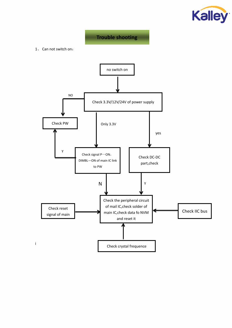
1、 Can not switch on:
i
NO
yes
Only 3.3V
Y
N Y
Check crystal frequence
Check IIC bus
Check the peripheral circuit of mail IC,check solder of
main IC,check data fo NVM and reset it
Check reset signal of main
no switch on
Check 3.3V/12V/24V of power supply
Check PW
Check DC-DC part,check
Check signal P—ON,
DIMBL—ON of main IC link
to PW
Trouble shooting

2、abnormal picture :
Check LVDS signal to main IC?check LVDS cable?
Check crystal frequence?
Check the peripheral circuit of mail IC,updating SW,reset NVM,replace main IC
Abnormal picture
All signal source bad Individual signal source bad
Check the path with this signal source Check panel ID?
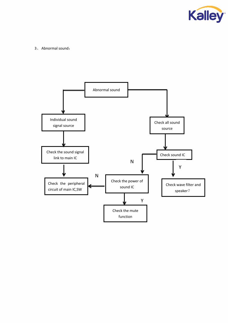
3、 Abnormal sound:
Y
N
N
Check the mute function
Abnormal sound
Check all sound source
Individual sound signal source
Check the sound signal link to main IC
Check the peripheral circuit of main IC,SW
Check the power of sound IC
Check sound IC
Check wave filter and speaker?
Y