Embed Size (px)
Citation preview
KeyStone ArchitectureGigabit Ethernet (GbE) Switch Subsystem
User's Guide
Literature Number: SPRUGV9DNovember 2010–Revised June 2013
2 SPRUGV9D–November 2010–Revised June 2013Submit Documentation Feedback
Copyright © 2010–2013, Texas Instruments Incorporated
Contents
Contents
Preface....................................................................................................................................... 161 Introduction ....................................................................................................................... 17
1.1 Purpose of the Peripheral ................................................................................................. 181.2 Features ..................................................................................................................... 181.3 Gigabit Ethernet Switch Subsystem Functional Block Diagram...................................................... 191.4 Industry Standard(s) Compliance Statement ........................................................................... 21
2 Architecture....................................................................................................................... 222.1 Clock Control................................................................................................................ 23
2.1.1 Gigabit Switch Subsystem Clock................................................................................ 232.1.2 SGMII SerDes Reference Clock................................................................................. 232.1.3 MDIO Clock ........................................................................................................ 232.1.4 IEEE 1588 Time Synchronization Clock ....................................................................... 232.1.5 GMII Clock ......................................................................................................... 23
2.2 Memory Map ................................................................................................................ 242.3 Gigabit Ethernet Switch Architecture .................................................................................... 24
2.3.1 Streaming Packet Interface ...................................................................................... 252.3.1.1 Transmit Streaming Packet Interface .................................................................... 252.3.1.2 Receive Streaming Packet Interface .................................................................... 26
2.3.2 Media Access Controller Submodule Architecture............................................................ 272.3.2.1 Data Receive Operations .................................................................................. 272.3.2.2 Data Transmission .......................................................................................... 28
2.3.3 MAC Receive FIFO Architecture ................................................................................ 322.3.4 Statistics Submodule Architecture .............................................................................. 33
2.3.4.1 Accessing Statistics Registers ............................................................................ 332.3.4.2 Statistics Interrupts ......................................................................................... 332.3.4.3 Receive Statistics Descriptions ........................................................................... 342.3.4.4 Transmit (Only) Statistics Descriptions .................................................................. 392.3.4.5 Receive and Transmit (Shared) Statistics Descriptions ............................................... 42
2.3.5 Time Synchronization Submodule Architecture ............................................................... 432.3.5.1 KeyStone II Time Synchronization Submodule Architecture .......................................... 442.3.5.2 Time Synchronization Submodule Components ........................................................ 442.3.5.3 Time Synchronization Events ............................................................................. 462.3.5.4 Time Synchronization Initialization ....................................................................... 512.3.5.5 Detecting and Processing Time Synchronization Events.............................................. 51
2.3.6 Address Lookup Engine (ALE) Submodule Architecture..................................................... 522.3.6.1 ALE Table .................................................................................................... 532.3.6.2 Reading Entries from the ALE Table ..................................................................... 532.3.6.3 Writing Entries to the ALE Table.......................................................................... 532.3.6.4 ALE Table Entry Types .................................................................................... 542.3.6.5 ALE Packet Forwarding Process ......................................................................... 582.3.6.6 ALE Learning Process...................................................................................... 64
2.4 Serial Gigabit Media Independent Interface (SGMII) Architecture................................................... 652.4.1 SGMII Receive Interface ......................................................................................... 652.4.2 SGMII Transmit Interface......................................................................................... 652.4.3 Modes of Operation ............................................................................................... 65
www.ti.com
3SPRUGV9D–November 2010–Revised June 2013Submit Documentation Feedback
Copyright © 2010–2013, Texas Instruments Incorporated
Contents
2.4.3.1 Digital Loopback ............................................................................................ 652.4.3.2 SGMII to PHY Configuration............................................................................... 662.4.3.3 SGMII to SGMII with Auto-Negotiation Configuration .................................................. 662.4.3.4 SGMII to SGMII with Forced Link Configuration ........................................................ 67
2.5 Management Data Input/Output (MDIO) Architecture ................................................................. 682.5.1 Global PHY Detection and Link State Monitoring ............................................................. 682.5.2 PHY Register User Access ...................................................................................... 68
2.5.2.1 Writing Data to a PHY Register ........................................................................... 692.5.2.2 Reading Data from a PHY Register ...................................................................... 70
2.5.3 MDIO Interrupts.................................................................................................... 702.5.3.1 MDIO User Access Interrupts ............................................................................. 70
2.5.4 Initializing the MDIO Module ..................................................................................... 702.6 KeyStone I Serializer/Deserializer (SerDes) Architecture............................................................. 712.7 KeyStone II Serializer/Deserializer (SerDes) Architecture ............................................................ 712.8 Reset Considerations ...................................................................................................... 712.9 Initialization.................................................................................................................. 71
2.9.1 GbE Switch Subsystem Initialization Procedure .............................................................. 712.10 Interrupt Support ........................................................................................................... 72
2.10.1 Interrupt Events................................................................................................... 722.11 Power Management........................................................................................................ 72
3 Registers........................................................................................................................... 733.1 Summary of Modules ...................................................................................................... 743.2 Gigabit Ethernet (GbE) Switch Subsystem Module.................................................................... 88
3.2.1 Ethernet Switch Subsystem Identification and Version Register (ES_SS_IDVER)....................... 893.3 Serial Gigabit Media Independent Interface (SGMII) module ........................................................ 90
3.3.1 SGMII Identification and Version Register (SGMII_IDVER) ................................................. 913.3.2 SGMII Software Reset Register (SGMII_SOFT_RESET).................................................... 923.3.3 SGMII Control Register (SGMII_CONTROL) .................................................................. 933.3.4 SGMII Status Register (SGMII_STATUS) ..................................................................... 943.3.5 SGMII Advertised Ability Register (SGMII_MR_ADV_ABILITY) ............................................ 95
3.3.5.1 SGMII MODE ................................................................................................ 953.3.6 SGMII Link Partner Advertised Ability Register (SGMII_MR_LP_ADV_ABILITY) ........................ 96
3.4 Management Data Input/Output (MDIO) module....................................................................... 973.4.1 MDIO Version Register (MDIO_VERSION).................................................................... 983.4.2 MDIO Control Register (MDIO_CONTROL) ................................................................... 993.4.3 PHY Alive Status Register (MDIO_ALIVE) ................................................................... 1003.4.4 PHY Link Status Register (MDIO_LINK)...................................................................... 1013.4.5 MDIO Link Status Change Interrupt (Unmasked) Register (MDIO_LINKINTRAW)..................... 1023.4.6 MDIO Link Status Change Interrupt (Masked) Register (MDIO_LINKINTMASKED) ................... 1033.4.7 MDIO User Command Complete Interrupt (Unmasked) Register (MDIO_USERINTRAW)............ 1043.4.8 MDIO User Command Complete Interrupt (Masked) Register (MDIO_USERINTMASKED) .......... 1053.4.9 MDIO User Command Complete Interrupt Mask Set Register (MDIO_USERINTMASKSET) ........ 1063.4.10 MDIO User Command Complete Interrupt Mask Clear Register (MDIO_USERINTMASKCLEAR) . 1073.4.11 MDIO User Access Register 0 (MDIO_USERACCESS0)................................................. 1083.4.12 MDIO User PHY Select Register 0 (MDIO_USERPHYSEL0) ............................................ 1093.4.13 MDIO User Access Register 1 (MDIO_USERACCESS1)................................................. 1103.4.14 MDIO User PHY Select Register 1 (MDIO_USERPHYSEL1) ............................................ 111
3.5 Ethernet Switch Module.................................................................................................. 1123.5.1 Gigabit Ethernet (GbE) Switch Submodule................................................................... 113
3.5.1.1 GbE Switch Identification and Version Register (CPSW_IDVER) .................................. 1163.5.1.2 GbE Switch Control Register (CPSW_CONTROL) ................................................... 1173.5.1.3 Emulation Control Register (EM_CONTROL) ......................................................... 1183.5.1.4 Statistics Port Enable (STAT_PORT_EN) ............................................................. 119
www.ti.com
4 SPRUGV9D–November 2010–Revised June 2013Submit Documentation Feedback
Copyright © 2010–2013, Texas Instruments Incorporated
Contents
3.5.1.5 Priority Type Register (PTYPE) ......................................................................... 1213.5.1.6 KeyStone I and KeyStone II MAC Short Gap Threshold Register (GAP_THRESH) ............. 1223.5.1.7 Transmit FIFO Start Words Register (TX_START_WDS) ........................................... 1233.5.1.8 Flow Control Register (FLOW_CONTROL) ............................................................ 1243.5.1.9 Port 0 Source Identification Register (P0_CPPI_SRC_ID) .......................................... 1253.5.1.10 Port 0 VLAN Register (P0_PORT_VLAN).............................................................. 1263.5.1.11 Port 0 Receive Packet Priority to Header Priority Mapping Register (P0_RX_PRI_MAP) ...... 1273.5.1.12 Port 0 Receive Maximum Length Register (P0_RX_MAXLEN) ..................................... 1283.5.1.13 Port 1 Max Blocks Register (P1_MAX_BLKS)......................................................... 1293.5.1.14 Port 1 Block Count Register (P1_BLK_CNT) .......................................................... 1303.5.1.15 Port 1 VLAN Register (P1_PORT_VLAN).............................................................. 1313.5.1.16 Port 1 Transmit Header Priority to Switch Priority Mapping Register (P1_TX_PRI_MAP) ...... 1323.5.1.17 MAC1 Source Address Low Register (MAC1_SA_LO)............................................... 1333.5.1.18 MAC1 Source Address High Register (MAC1_SA_HI)............................................... 1343.5.1.19 Port 1 Time Sync Control Register (P1_TS_CTL) .................................................... 1353.5.1.20 Port 1 Time Sync Sequence ID and LTYPE Register (P1_TS_SEQ_LTYPE) .................... 1373.5.1.21 Port 1 Time Sync Control Register 2 (P1 _TS_CTL2)................................................ 1383.5.1.22 Port 1 Time Sync Control Register and LTYPE2 (P1 _TS_CTL_LTYPE2)........................ 1393.5.1.23 Port 1 Time Sync VLAN LTYPE Register (P1_TS_VLAN_LTYPE)................................. 1403.5.1.24 Port 2 Max Blocks Register (P2_MAX_BLKS)......................................................... 1413.5.1.25 Port 2 Block Count Register (P2_BLK_CNT) .......................................................... 1423.5.1.26 Port 2 VLAN Register (P2_PORT_VLAN).............................................................. 1433.5.1.27 Port 2 Transmit Header Priority to Switch Priority Mapping Register (P2_TX_PRI_MAP) ...... 1443.5.1.28 MAC2 Source Address Low Register (MAC2_SA_LO)............................................... 1453.5.1.29 MAC2 Source Address High Reserved Register (MAC2_SA_HI) .................................. 1463.5.1.30 Port 2 Time Sync Control Register (P2_TS_CTL) .................................................... 1473.5.1.31 Port 2 Time Sync Sequence ID and LTYPE Register (P2_TS_SEQ_LTYPE) .................... 1493.5.1.32 Port 2 Time Sync VLAN LTYPE Register (P2_TS_VLAN_LTYPE)................................. 1503.5.1.33 Port 2 Time Sync Control Register 2 (P2 _TS_CTL2)................................................ 1513.5.1.34 Port 2 Time Sync Control Register and LTYPE2 (P2 _TS_CTL_LTYPE2)........................ 152
3.5.2 KeyStone II Port 3 & 4 Register Descriptions................................................................ 1533.5.2.1 Port 3 Max Blocks Register (P3_MAX_BLKS)......................................................... 1533.5.2.2 Port 3 Block Count Register (P3_BLK_CNT) .......................................................... 1543.5.2.3 Port 3 VLAN Register (P3_PORT_VLAN).............................................................. 1553.5.2.4 Port 3 Transmit Header Priority to Switch Priority Mapping Register (P3_TX_PRI_MAP) ...... 1563.5.2.5 MAC3 Source Address Low Register (MAC3_SA_LO)............................................... 1573.5.2.6 MAC3 Source Address High Register (MAC3_SA_HI)............................................... 1583.5.2.7 Port 3 Time Sync Control Register (P3 _TS_CTL) ................................................... 1593.5.2.8 Port 3 Time Sync Sequence ID and LTYPE Register (P3_TS_SEQ_LTYPE) .................... 1603.5.2.9 Port 3 Time Sync VLAN LTYPE Register (P3_TS_VLAN_LTYPE)................................. 1613.5.2.10 Port 3 Time Sync Control and LTYPE2 Register (P3 _TS_CTL_LTYPE2)........................ 1623.5.2.11 Port 3 Time Sync Control Register 2 (P3 _TS_CTL2)................................................ 1633.5.2.12 Port 4 Max Blocks Register (P4_MAX_BLKS)......................................................... 1643.5.2.13 Port 4 Block Count Register (P4_BLK_CNT) .......................................................... 1653.5.2.14 Port 4 VLAN Register (P4_PORT_VLAN).............................................................. 1663.5.2.15 Port 4 Transmit Header Priority to Switch Priority Mapping Register (P4_TX_PRI_MAP) ...... 1673.5.2.16 MAC4 Source Address Low Register (MAC4_SA_LO)............................................... 1683.5.2.17 MAC4 Source Address High Register (MAC4_SA_HI)............................................... 1693.5.2.18 Port 4 Time Sync Control Register (P4 _TS_CTL) ................................................... 1703.5.2.19 Port 4 Time Sync Sequence ID and LTYPE Register (P4_TS_SEQ_LTYPE) .................... 1713.5.2.20 Port 4 Time Sync VLAN LTYPE Register (P4_TS_VLAN_LTYPE)................................. 1723.5.2.21 Port 4 Time Sync Control Register and LTYPE2 (P4 _TS_CTL_LTYPE2)........................ 1733.5.2.22 Port 4 Time Sync Control Register 2 (P4 _TS_CTL2)................................................ 174
www.ti.com
5SPRUGV9D–November 2010–Revised June 2013Submit Documentation Feedback
Copyright © 2010–2013, Texas Instruments Incorporated
Contents
3.5.3 Ethernet Media Access Controller (EMAC) Submodule .................................................... 1753.5.3.1 MAC Identification and Version Register (MAC_IDVER)............................................. 1763.5.3.2 MAC Control Register (MAC_CONTROL) ............................................................. 1773.5.3.3 MAC Status Register (MACSTATUS) .................................................................. 1793.5.3.4 Software Reset Register (SOFT_RESET) ............................................................. 1803.5.3.5 Receive Maximum Length Register (RX_MAXLEN) .................................................. 1813.5.3.6 Receive Pause Timer Register (RX_PAUSE) ......................................................... 1823.5.3.7 Transmit Pause Timer Register (TX_PAUSE)......................................................... 1833.5.3.8 Emulation Control Register (EM_CONTROL) ......................................................... 1843.5.3.9 Receive Packet Priority to Header Priority Mapping Register (MAC_RX_PRI_MAP) ............ 185
3.5.4 Statistics (STATS) Submodule................................................................................. 1863.5.4.1 Port n Good Receive Frames Register (STATn_RXGOODFRAMES) ............................. 1883.5.4.2 Broadcast Receive Frames Register (RXBROADCASTFRAMES) ................................. 1893.5.4.3 Multicast Receive Frames Register (RXMULTICASTFRAMES) .................................... 1903.5.4.4 Pause Receive Frames Register (RXPAUSEFRAMES) ............................................. 1913.5.4.5 Receive CRC Errors Register ( RXCRCERRORS) ................................................... 1923.5.4.6 Receive Align/Code Errors Register (RXALIGNCODEERRORS) .................................. 1933.5.4.7 Oversize Receive Frames Register (RXOVERSIZEDFRAMES).................................... 1943.5.4.8 Receive Jabber Frames Register (RXJABBERFRAMES) ........................................... 1953.5.4.9 Undersize (Short) Receive Frames Register (RXUNDERSIZEDFRAMES) ....................... 1963.5.4.10 Receive Fragment Register (RXFRAGMENTS)....................................................... 1973.5.4.11 Port n Receive Octets Register (STATn_RXOCTETS)............................................... 1983.5.4.12 Good Transmit Frames Register (TXGOODFRAMES)............................................... 1993.5.4.13 Broadcast Transmit Frames Register (TXBROADCASTFRAMES)................................. 2003.5.4.14 Multicast Transmit Frames (TXMULTICASTFRAMES) .............................................. 2013.5.4.15 Pause Transmit Frames Register (TXPAUSEFRAMES)............................................. 2023.5.4.16 Deferred Transmit Frames Register (TXDEFERREDFRAMES) .................................... 2033.5.4.17 Transmit Frames Collision Register (TXCOLLISIONFRAMES) ..................................... 2043.5.4.18 Transmit Frames Single Collision Register (TXSINGLECOLLFRAMES) .......................... 2053.5.4.19 Transmit Frames Multiple Collision Register (TXMULTCOLLFRAMES) ........................... 2063.5.4.20 Transmit Excessive Collision Register (TXEXCESSIVECOLLISIONS) ............................ 2073.5.4.21 Transmit Late Collisions Register (TXLATECOLLISIONS) .......................................... 2083.5.4.22 Transmit Frames Underrun Register (TXUNDERRUN) .............................................. 2093.5.4.23 Transmit Carrier Sense Errors Register (TXCARRIERSENSEERRORS) ......................... 2103.5.4.24 Transmit Octets Register (TXOCTETS) ................................................................ 2113.5.4.25 Receive and Transmit 64 Octet Frames Register (64OCTETFRAMES)........................... 2123.5.4.26 Receive and Transmit 65-127 Octet Frames Register (65T127OCTETFRAMES) ............... 2133.5.4.27 Receive and Transmit 128-255 Octet Frames Register (128T255OCTETFRAMES) ............ 2143.5.4.28 Receive and Transmit 256-511 Octet Frames Register (256T511OCTETFRAMES) ............ 2153.5.4.29 Receive and Transmit 512-1023 Octet Frames Register (512T1023OCTETFRAMES) ......... 2163.5.4.30 Receive and Transmit 1024 and Up Octet Frames Register (1024TUPOCTETFRAMES)...... 2173.5.4.31 Net Octets Register (NETOCTETS) .................................................................... 2183.5.4.32 Receive Start of Frame Overruns Register (RXSOFOVERRUNS) ................................. 2193.5.4.33 Receive Middle of Frame Overruns Register (RXMOFOVERRUNS) .............................. 2203.5.4.34 Receive DMA Overruns Register (RXDMAOVERRUNS) ............................................ 221
3.5.5 Time Synchronization (CPTS) Submodule ................................................................... 2223.5.5.1 CPTS Identification and Version Register (CPTS_IDVER) .......................................... 2233.5.5.2 Time Sync Control Register (CPTS_CTL) ............................................................. 2243.5.5.3 RFTCLK Select Register (CPTS_RFTCLK_SEL) ..................................................... 2253.5.5.4 Time Stamp Event Push Register (CPTS_TS_PUSH) ............................................... 2263.5.5.5 Interrupt Status Raw Register (CPTS_INTSTAT_RAW) ............................................. 2273.5.5.6 Interrupt Status Masked Register (CPTS_INTSTAT_MASKED) .................................... 2283.5.5.7 Interrupt Enable Register (CPTS_INT_ENABLE) ..................................................... 229
www.ti.com
6 SPRUGV9D–November 2010–Revised June 2013Submit Documentation Feedback
Copyright © 2010–2013, Texas Instruments Incorporated
Contents
3.5.5.8 Event Pop Register (CPTS_EVENT_POP) ............................................................ 2303.5.5.9 Event Low Register (CPTS_EVENT_LOW)............................................................ 2313.5.5.10 Event Middle Register (CPTS_EVENT_MID).......................................................... 2323.5.5.11 Event High Register (CPTS_EVENT_HIGH) .......................................................... 233
3.5.6 Address Lookup Engine (ALE) submodule ................................................................... 2343.5.6.1 ALE Identification and Version Register (ALE_IDVER) .............................................. 2353.5.6.2 ALE Control Register (ALE_CONTROL) ............................................................... 2363.5.6.3 ALE Prescale Register (ALE_PRESCALE) ............................................................ 2383.5.6.4 ALE Unknown VLAN Register (UNKNOWN_VLAN).................................................. 2393.5.6.5 ALE Table Control Register (ALE_TBLCTL)........................................................... 2403.5.6.6 ALE Table Word 2 Register (ALE_TBLW2)............................................................ 2413.5.6.7 ALE Table Word 1 Register (ALE_TBLW1)............................................................ 2423.5.6.8 ALE Table Word 0 Register (ALE_TBLW0)............................................................ 2433.5.6.9 ALE Port 0 Control Register (ALE_PORTCTL0) ...................................................... 2443.5.6.10 ALE Port 1 Control Register (ALE_PORTCTL1) ...................................................... 2453.5.6.11 ALE Port 2 Control Register (ALE_PORTCTL2) ...................................................... 2463.5.6.12 ALE Port 3 Control Register (ALE_PORTCTL3) ...................................................... 2473.5.6.13 ALE Port 4 Control Register (ALE_PORTCTL4) ...................................................... 2483.5.6.14 ALE Port 5 Control Register (ALE_PORTCTL5) ...................................................... 249
3.6 Serializer/Deserializer (SerDes) SGMII Boot Configuration Registers............................................. 2503.6.1 SGMII SerDes Status Register (SGMII_SERDES_STS) ................................................... 2513.6.2 SGMII PLL Configuration Register (SGMII_SERDES_CFGPLL) ......................................... 2523.6.3 SGMII Receive Configuration Register n (SGMII_SERDES_CFGRX n)................................. 2543.6.4 SGMII Transmit Configuration Register n (SGMII_SERDES_CFGTX n) ................................ 256
Revision History ........................................................................................................................ 258
www.ti.com
7SPRUGV9D–November 2010–Revised June 2013Submit Documentation Feedback
Copyright © 2010–2013, Texas Instruments Incorporated
List of Figures
List of Figures1-1. KeyStone I Ethernet Switch Subsystem Block Diagram .............................................................. 191-2. KeyStone II Ethernet Switch Subsystem Block Diagram ............................................................. 202-1. Free Table Entry............................................................................................................ 542-2. Multicast Address Table Entry............................................................................................ 542-3. VLAN/Multicast Table Entry............................................................................................... 552-4. Unicast Table Entry ........................................................................................................ 552-5. OUI Unicast Table Entry................................................................................................... 562-6. VLAN/Unicast Table Entry ................................................................................................ 562-7. VLAN Table Entry .......................................................................................................... 572-8. SGMII Mode with PHY Configuration.................................................................................... 662-9. SGMII Master to SGMII Slave with Auto-Negotiation Configuration................................................. 662-10. SGMII Master to SGMII Master with Forced Link Configuration ..................................................... 673-1. Ethernet Switch Subsystem Identification and Version Register (ES_SS_IDVER)................................ 893-2. SGMII Identification and Version Register (SGMII_IDVER) .......................................................... 913-3. SGMII Software Reset Register (SGMII_SOFT_RESET) ............................................................ 923-4. SGMII Control Register (SGMII_CONTROL) ........................................................................... 933-5. SGMII Status Register (SGMII_STATUS) .............................................................................. 943-6. SGMII Advertised Ability Register (SGMII_MR_ADV_ABILITY) ..................................................... 953-7. SGMII Link Partner Advertised Ability Register (SGMII_MR_LP_ADV_ABILITY) ................................. 963-8. MDIO Version Register (MDIO_VERSION)............................................................................. 983-9. MDIO Control Register (MDIO_CONTROL) ............................................................................ 993-10. PHY Alive Status Register (MDIO_ALIVE) ............................................................................ 1003-11. PHY Link Status Register (MDIO_LINK)............................................................................... 1013-12. MDIO Link Status Change Interrupt (Unmasked) Register (MDIO_LINKINTRAW).............................. 1023-13. MDIO Link Status Change Interrupt (Masked) Register (MDIO_LINKINTMASKED) ............................ 1033-14. MDIO User Command Complete Interrupt (Unmasked) Register (MDIO_USERINTRAW)..................... 1043-15. MDIO User Command Complete Interrupt (Masked) Register (MDIO_USERINTMASKED) ................... 1053-16. MDIO User Command Complete Interrupt Mask Set Register (MDIO_USERINTMASKSET) ................. 1063-17. MDIO User Command Complete Interrupt Mask Clear Register (MDIO_USERINTMASKCLEAR) ........... 1073-18. MDIO User Access Register 0 (MDIO_USERACCESS0) ........................................................... 1083-19. MDIO User PHY Select Register 0 (MDIO_USERPHYSEL0) ...................................................... 1093-20. MDIO User Access Register 1 (MDIO_USERACCESS1) ........................................................... 1103-21. MDIO User PHY Select Register 1 (MDIO_USERPHYSEL1) ...................................................... 1113-22. GbE Switch Identification and Version Register (CPSW_IDVER).................................................. 1163-23. GbE Switch Control Register (CPSW_CONTROL) .................................................................. 1173-24. Emulation Control Register (EM_CONTROL)......................................................................... 1183-25. KeyStone I Statistics Port Enable (STAT_PORT_EN)............................................................... 1193-26. KeyStone II Statistics Port Enable (STAT_PORT_EN) .............................................................. 1193-27. KeyStone I Priority Type Register (PTYPE)........................................................................... 1213-28. KeyStone II Priority Type Register (PTYPE) .......................................................................... 1213-29. KeyStone I and KeyStone II MAC Short Gap Threshold Register (GAP_THRESH) ............................ 1223-30. Transmit FIFO Start Words Register (TX_START_WDS)........................................................... 1233-31. KeyStone I Flow Control Register (FLOW_CONTROL) ............................................................. 1243-32. KeyStone II Flow Control Register (FLOW_CONTROL) ............................................................ 1243-33. KeyStone I Port 0 Source Identification Register (P0_CPPI_SRC_ID)............................................ 1253-34. KeyStone II Port 0 Source Identification Register (P0_CPPI_SRC_ID) ........................................... 1253-35. Port 0 VLAN Register (P0_PORT_VLAN) ............................................................................. 126
www.ti.com
8 SPRUGV9D–November 2010–Revised June 2013Submit Documentation Feedback
Copyright © 2010–2013, Texas Instruments Incorporated
List of Figures
3-36. Port 0 Receive Packet Priority to Header Priority Mapping Register (P0_RX_PRI_MAP)...................... 1273-37. Port 0 RX Maximum Length Register (P0_RX_MAXLEN) .......................................................... 1283-38. Port 1 Max Blocks Register (P1_MAX_BLKS) ........................................................................ 1293-39. Port 1 Block Count Register (P1_BLK_CNT) ......................................................................... 1303-40. Port 1 VLAN Register (P1_PORT_VLAN) ............................................................................. 1313-41. Port 1 Transmit Header Priority to Switch Priority Mapping Register (P1_TX_PRI_MAP)...................... 1323-42. MAC1 Source Address Low Register (MAC1_SA_LO) .............................................................. 1333-43. MAC1 Source Address High Register (MAC1_SA_HI) .............................................................. 1343-44. KeyStone I Port 1 Time Sync Control Register (P1_TS_CTL)...................................................... 1353-45. KeyStone II Port 1 Time Sync Control Register (P1_TS_CTL)..................................................... 1363-46. Port 1 Time Sync Sequence ID and LTYPE Register (P1_TS_SEQ_LTYPE) ................................... 1373-47. Port 1 Time Sync Control Register 2 (P1_TS_CTL2)................................................................ 1383-48. Port 1 Time Sync Control Register and LTYPE2 (P1_TS_CTL_LTYPE2) ........................................ 1393-49. Port 1 Time Sync VLAN LTYPE Register (P1_TS_VLAN_LTYPE) ................................................ 1403-50. Port 2 Max Blocks Register (P2_MAX_BLKS) ........................................................................ 1413-51. Port 2 Block Count Register (P2_BLK_CNT) ......................................................................... 1423-52. Port 2 VLAN Register (P2_PORT_VLAN) ............................................................................. 1433-53. Port 2 Transmit Header Priority to Switch Priority Mapping Register (P2_TX_PRI_MAP)...................... 1443-54. MAC2 Source Address Low Register (MAC2_SA_LO) .............................................................. 1453-55. MAC2 Source Address High Reserved Register (MAC2_SA_HI).................................................. 1463-56. KeyStone I Port 2 Time Sync Control Register (P2_TS_CTL)...................................................... 1473-57. KeyStone II Port 2 Time Sync Control Register (P1_TS_CTL)..................................................... 1483-58. Port 2 Time Sync Sequence ID and LTYPE Register (P2_TS_SEQ_LTYPE) ................................... 1493-59. Port 2 Time Sync VLAN LTYPE Register (P2_TS_VLAN_LTYPE) ................................................ 1503-60. Port 2Time Sync Control Register 2 (P3_TS_CTL2)................................................................. 1513-61. Port 2 Time Sync Control Register and LTYPE2 (P2_TS_CTL_LTYPE2) ........................................ 1523-62. Port 3 Max Blocks Register (P3_MAX_BLKS) ........................................................................ 1533-63. Port 3 Block Count Register (P3_BLK_CNT) ......................................................................... 1543-64. Port 3 VLAN Register (P3_PORT_VLAN) ............................................................................. 1553-65. Port 3 Transmit Header Priority to Switch Priority Mapping Register (P3_TX_PRI_MAP)...................... 1563-66. MAC3 Source Address Low Register (MAC3_SA_LO) .............................................................. 1573-67. MAC3 Source Address High Register (MAC3_SA_HI) .............................................................. 1583-68. Port 3 Time Sync Control Register (P3_TS_CTL).................................................................... 1593-69. Port 3 Time Sync Sequence ID and LTYPE Register (P3_TS_SEQ_LTYPE) ................................... 1603-70. Port 3 Time Sync VLAN LTYPE Register (P3_TS_VLAN_LTYPE) ................................................ 1613-71. Port 3 Time Sync Control and LTYPE2 Register (P3_TS_CTL_LTYPE2) ........................................ 1623-72. Port 3 Time Sync Control Register 2 (P3_TS_CTL2)................................................................ 1633-73. Port 4 Max Blocks Register (P4_MAX_BLKS) ........................................................................ 1643-74. Port 4 Block Count Register (P4_BLK_CNT) ......................................................................... 1653-75. Port 4 VLAN Register (P4_PORT_VLAN) ............................................................................. 1663-76. Port 4 Transmit Header Priority to Switch Priority Mapping Register (P4_TX_PRI_MAP)...................... 1673-77. MAC4 Source Address Low Register (MAC4_SA_LO) .............................................................. 1683-78. MAC4 Source Address High Register (MAC4_SA_HI) .............................................................. 1693-79. Port 4 Time Sync Control Register (P4_TS_CTL).................................................................... 1703-80. Port 4 Time Sync Sequence ID and LTYPE Register (P4_TS_SEQ_LTYPE) ................................... 1713-81. Port 4 Time Sync VLAN LTYPE Register (P4_TS_VLAN_LTYPE) ................................................ 1723-82. Port 4 Time Sync Control Register and LTYPE2 (P4_TS_CTL_LTYPE2) ........................................ 1733-83. Port 4 Time Sync Control Register 2 (P4_TS_CTL2)................................................................ 1743-84. MAC Identification and Version Register (MAC_IDVER) ........................................................... 176
www.ti.com
9SPRUGV9D–November 2010–Revised June 2013Submit Documentation Feedback
Copyright © 2010–2013, Texas Instruments Incorporated
List of Figures
3-85. MAC Control Register (MAC_CONTROL)............................................................................. 1773-86. MAC Status Register (MACSTATUS).................................................................................. 1793-87. Software Reset Register (SOFT_RESET)............................................................................. 1803-88. Receive Maximum Length Register (RX_MAXLEN) ................................................................. 1813-89. Receive Pause Timer Register (RX_PAUSE)......................................................................... 1823-90. Transmit Pause Timer Register (TX_PAUSE) ........................................................................ 1833-91. Emulation Control Register (EM_CONTROL) ........................................................................ 1843-92. Receive Packet Priority to Header Priority Mapping Register (MAC_RX_PRI_MAP) ........................... 1853-93. Port n Good Receive Frames Register (STATn_RXGOODFRAMES)............................................. 1883-94. Broadcast Receive Frames Register (RXBROADCASTFRAMES) ................................................ 1893-95. Multicast Receive Frames Register (RXMULTICASTFRAMES) ................................................... 1903-96. Pause Receive Frames Register (RXPAUSEFRAMES)............................................................. 1913-97. Receive CRC Errors Register (RXCRCERRORS) ................................................................... 1923-98. Receive Align/Code Errors Register (RXALIGNCODEERRORS).................................................. 1933-99. Oversize Receive Frames Register (RXOVERSIZEDFRAMES) ................................................... 1943-100. Receive Jabber Frames Register (RXJABBERFRAMES)........................................................... 1953-101. Undersize (Short) Receive Frames Register (RXUNDERSIZEDFRAMES)....................................... 1963-102. Receive Fragment Register (RXFRAGMENTS) ...................................................................... 1973-103. Port n Receive Octets Register (STATn_RXOCTETS) .............................................................. 1983-104. Good Transmit Frames Register (TXGOODFRAMES) .............................................................. 1993-105. Broadcast Transmit Frames Register ( TXBROADCASTFRAMES) ............................................... 2003-106. Multicast Transmit Frames (TXMULTICASTFRAMES).............................................................. 2013-107. Pause Transmit Frames Register (TXPAUSEFRAMES) ............................................................ 2023-108. Deferred Transmit Frames Register (TXDEFERREDFRAMES).................................................... 2033-109. Transmit Frames Collision Register (TXCOLLISIONFRAMES) .................................................... 2043-110. Transmit Frames Single Collision Register (TXSINGLECOLLFRAMES) ......................................... 2053-111. Transmit Frames Multiple Collision Register (TXMULTCOLLFRAMES) .......................................... 2063-112. Transmit Excessive Collision Register (TXEXCESSIVECOLLISIONS) ........................................... 2073-113. Transmit Late Collisions Register (TXLATECOLLISIONS).......................................................... 2083-114. Transmit Frames Underrun Register (TXUNDERRUN) ............................................................. 2093-115. Transmit Carrier Sense Errors Register (TXCARRIERSENSEERRORS) ........................................ 2103-116. Transmit Octets Register (TXOCTETS) ............................................................................... 2113-117. Receive and Transmit 64 Octet Frames Register (64OCTETFRAMES) .......................................... 2123-118. Receive and Transmit 65-127 Octet Frames Register (65T127OCTETFRAMES) .............................. 2133-119. Receive and Transmit 128-255 Octet Frames Register (128T255OCTETFRAMES) ........................... 2143-120. Receive and Transmit 256-511 Octet Frames Register (256T511OCTETFRAMES) ........................... 2153-121. Receive and Transmit 512-1023 Octet Frames Register (512T1023OCTETFRAMES) ........................ 2163-122. Receive and Transmit 1024 and Up Octet Frames Register (1024TUPOCTETFRAMES) ..................... 2173-123. Net Octets Register (NETOCTETS).................................................................................... 2183-124. Receive Start of Frame Overruns Register (RXSOFOVERRUNS) ................................................ 2193-125. Receive Middle of Frame Overruns Register (RXMOFOVERRUNS).............................................. 2203-126. Receive DMA Overruns Register (RXDMAOVERRUNS) ........................................................... 2213-127. CPTS Identification and Version Register (CPTS_IDVER) ......................................................... 2233-128. Time Sync Control Register (TS_CTL) ................................................................................ 2243-129. RFTCLK Select Register (CPTS_RFTCLK_SEL) .................................................................... 2253-130. Time Stamp Event Push Register (CPTS_TS_PUSH) .............................................................. 2263-131. Interrupt Status Raw Register (CPTS_INTSTAT_RAW) ............................................................ 2273-132. Interrupt Status Masked Register (CPTS_INTSTAT_MASKED) ................................................... 2283-133. Interrupt Enable Register (CPTS_INT_ENABLE) .................................................................... 229
www.ti.com
10 SPRUGV9D–November 2010–Revised June 2013Submit Documentation Feedback
Copyright © 2010–2013, Texas Instruments Incorporated
List of Figures
3-134. Event Pop Register (CPTS_EVENT_POP) ........................................................................... 2303-135. Event Low Register (CPTS_EVENT_LOW) ........................................................................... 2313-136. Event MIddle Register (CPTS_EVENT_MID) ......................................................................... 2323-137. Event High Register (CPTS_EVENT_HIGH).......................................................................... 2333-138. ALE Identification and Version Register (ALE_IDVER).............................................................. 2353-139. ALE Control Register (ALE_CONTROL) .............................................................................. 2363-140. ALE Prescale Register (ALE_PRESCALE) ........................................................................... 2383-141. ALE Unknown VLAN Register (UNKNOWN_VLAN) ................................................................. 2393-142. ALE Table Control Register (ALE_TBLCTL) .......................................................................... 2403-143. ALE Table Word 2 Register (ALE_TBLW2) ........................................................................... 2413-144. ALE Table Word 1 Register (ALE_TBLW1) ........................................................................... 2423-145. ALE Table Word 0 Register (ALE_TBLW0) ........................................................................... 2433-146. ALE Port 0 Control Register (ALE_PORTCTL0) ..................................................................... 2443-147. ALE Port 1 Control Register (ALE_PORTCTL1) ..................................................................... 2453-148. ALE Port 2 Control Register (ALE_PORTCTL2) ..................................................................... 2463-149. ALE Port 3 Control Register (ALE_PORTCTL3) ..................................................................... 2473-150. ALE Port 4 Control Register (ALE_PORTCTL4) ..................................................................... 2483-151. ALE Port 5 Control Register (ALE_PORTCTL5) ..................................................................... 2493-152. SGMII SerDes Status Register (SGMII_SERDES_STS) ............................................................ 2513-153. SGMII PLL Configuration Register (SGMII_SERDES_CGFPLL) .................................................. 2523-154. SGMII Receive Configuration Register n (SGMII_SERDES_CFGRXn ) ....................................... 2543-155. SGMII Transmit Configuration Register n (SGMII_SERDES_CFGTXn ) ...................................... 256
www.ti.com
11SPRUGV9D–November 2010–Revised June 2013Submit Documentation Feedback
Copyright © 2010–2013, Texas Instruments Incorporated
List of Tables
List of Tables2-1. KeyStone I Gigabit Ethernet Switch Subsystem Modules ............................................................ 242-2. KeyStone II Gigabit Ethernet Switch Subsystem Modules ........................................................... 242-3. KeyStone I PS_FLAGS for GbE Switch Ingress Packets............................................................. 262-4. KeyStone II PS_FLAGS for GbE Switch Ingress Packets ............................................................ 262-5. KeyStone I Time Synchronization Event Fields ........................................................................ 462-6. KeyStone II Time Synchronization Event Fields ....................................................................... 462-7. ALE Table Learned Address Control Bits ............................................................................... 532-8. Free Table Entry Field Configuration .................................................................................... 542-9. Multicast Address Table Entry Field Configuration .................................................................... 542-10. VLAN/Multicast Address Table Entry Field Configuration ............................................................ 552-11. Unicast Address Table Entry Field Configuration ...................................................................... 552-12. OUI Unicast Address Table Entry Field Configuration ................................................................ 562-13. VLAN/Unicast Table Entry Field Configuration ......................................................................... 562-14. VLAN Table Entry Field Configuration................................................................................... 572-15. ALE Table Entry Field Descriptions ..................................................................................... 572-16. Gigabit Ethernet Switch Subsystem Descriptor Error Flags .......................................................... 592-17. ALE Ingress Filtering Process ............................................................................................ 602-18. ALE VLAN Aware Lookup Process ...................................................................................... 612-19. ALE VLAN Unaware Lookup Process ................................................................................... 622-20. ALE Egress Process ....................................................................................................... 632-21. ALE Learning Process ..................................................................................................... 643-1. KeyStone I Gigabit Ethernet Switch Subsystem Modules ............................................................ 743-2. KeyStone II Gigabit Ethernet Switch Subsystem Module ............................................................. 743-3. KeyStone I Gigabit Ethernet Switch Subsystem Complete Register Listing ....................................... 743-4. KeyStone II Gigabit Ethernet Switch Subsystem Complete Register Listing ...................................... 813-5. Ethernet Switch Subsystem Module .................................................................................... 883-6. Ethernet Switch Subsystem Identification and Version Register (ES_SS_IDVER) Field Descriptions ......... 893-7. SGMII Registers ........................................................................................................... 903-8. SGMII Identification and Version Register (SGMII_IDVER) Field Descriptions ................................... 913-9. SGMII Software Reset Register (SGMII_SOFT_RESET) Field Descriptions ...................................... 923-10. SGMII Control Register (SGMII_CONTROL) Field Descriptions .................................................... 933-11. SGMII Status Register (SGMII_STATUS) Field Descriptions ....................................................... 943-12. SGMII Advertised Ability Register (SGMII_MR_ADV_ABILITY) Field Descriptions .............................. 953-13. Advertised Ability and Link Partner Advertised Ability for SGMII Mode ............................................ 953-14. SGMII Link Partner Advertised Ability Register (SGMII_MR_LP_ADV_ABILITY) Field Descriptions........... 963-15. MDIO Registers ............................................................................................................ 973-16. MDIO Version Register (MDIO _VERSION) Field Descriptions ..................................................... 983-17. MDIO Control Register (MDIO_CONTROL) Field Descriptions...................................................... 993-18. PHY Alive Status Register (MDIO_ALIVE) Field Descriptions...................................................... 1003-19. PHY Link Status Register (MDIO_LINK) Field Descriptions ....................................................... 1013-20. MDIO Link Status Change Interrupt (Unmasked) Register (MDIO_LINKINTRAW) Field Descriptions ....... 1023-21. MDIO Link Status Change Interrupt (Masked) Register (MDIO_LINKINTMASKED) Field Descriptions ..... 1033-22. MDIO User Command Complete Interrupt (Unmasked) Register (MDIO_USERINTRAW) Field
Descriptions ............................................................................................................... 1043-23. MDIO User Command Complete Interrupt (Masked) Register (MDIO_USERINTMASKED) Field
Descriptions ............................................................................................................... 1053-24. MDIO User Command Complete Interrupt Mask Set Register (MDIO_USERINTMASKSET) Field
Descriptions ............................................................................................................... 106
www.ti.com
12 SPRUGV9D–November 2010–Revised June 2013Submit Documentation Feedback
Copyright © 2010–2013, Texas Instruments Incorporated
List of Tables
3-25. MDIO User Command Complete Interrupt Mask Clear Register (MDIO_USERINTMASKCLEAR) FieldDescriptions ............................................................................................................... 107
3-26. MDIO User Access Register 0 (MDIO_USERACCESS0) Field Descriptions .................................... 1083-27. MDIO User PHY Select Register 0 (MDIO_USERPHYSEL0) Field Descriptions ............................... 1093-28. MDIO User Access Register 1 (MDIO_USERACCESS1) Field Descriptions .................................... 1103-29. MDIO User PHY Select Register 1 (MDIO_USERPHYSEL1) Field Descriptions ............................... 1113-30. KeyStone I Ethernet Switch Submodules ............................................................................. 1123-31. KeyStone II Ethernet Switch Submodules ............................................................................ 1123-32. KeyStone I Ethernet Switch Registers ................................................................................. 1133-33. KeyStone II Ethernet Switch Registers ................................................................................ 1143-34. GbE Switch Identification and Version Register (CPSW_IDVER) Field Descriptions ........................... 1163-35. GbE Switch Control Register (CPSW_CONTROL) Field Descriptions for KeyStone I and KeyStone II ...... 1173-36. Emulation Control Register (EM_CONTROL) Field Descriptions ................................................. 1183-37. KeyStone I Statistics Port Enable (STAT_PORT_EN) Field Descriptions ........................................ 1193-38. KeyStone II Statistics Port Enable (STAT_PORT_EN) Field Descriptions ....................................... 1193-39. KeyStone I Priority Type Register (PTYPE) Field Descriptions .................................................... 1213-40. KeyStone II Priority Type Register (PTYPE) Field Descriptions ................................................... 1213-41. KeyStone I and KeyStone II MAC Short Gap Threshold Register (GAP_THRESH) Field Descriptions ..... 1223-42. Transmit FIFO Start Words Register (TX_START_WDS) Field Descriptions .................................... 1233-43. KeyStone I Flow Control Register (FLOW_CONTROL) Field Descriptions ...................................... 1243-44. KeyStone II Flow Control Register (FLOW_CONTROL) Field Descriptions ..................................... 1243-45. KeyStone I Port 0 Source Identification Register (P0_CPPI_SRC_ID) Field Descriptions ..................... 1253-46. KeyStone II Port 0 Source Identification Register (P0_CPPI_SRC_ID) Field Descriptions .................... 1253-47. Port 0 VLAN Register (P0_PORT_VLAN) Field Descriptions ...................................................... 1263-48. Port 0 Receive Packet Priority to Header Priority Mapping Register (P0_RX_PRI_MAP) Field
Descriptions ............................................................................................................... 1273-49. Port 0 RX Maximum Length Register (P0_RX_MAXLEN) Field Descriptions ................................... 1283-50. Port 1 Max Blocks Register (P1_MAX_BLKS) Field Descriptions ................................................. 1293-51. Port 1 Block Count Register (P1_BLK_CNT) Field Descriptions .................................................. 1303-52. Port 1 VLAN Register (P1_PORT_VLAN) Field Descriptions ...................................................... 1313-53. Port 1 Transmit Header Priority to Switch Priority Mapping Register (P1_TX_PRI_MAP) Field
Descriptions ............................................................................................................... 1323-54. MAC1 Source Address Low Register (MAC1_SA_LO) Field Descriptions ....................................... 1333-55. MAC1 Source Address High Register (MAC1_SA_HI) Field Descriptions ....................................... 1343-56. KeyStone I Port 1 Time Sync Control Register (P1_TS_CTL) Field Descriptions .............................. 1353-57. KeyStone II Port 1 Time Sync Control Register (P1_TS_CTL) Field Descriptions .............................. 1363-58. Port 1 Time Sync Sequence ID and LTYPE Register (P1_TS_SEQ_LTYPE) Field Descriptions ............ 1373-59. Port 1 Time Sync Control 2 Register (P1_TS_CTL2) Field Descriptions ......................................... 1383-60. Port 1Time Sync Control Register and LTYPE2 (P1_TS_CTL_LTYPE2) Field Descriptions (KeyStone II
Only) ........................................................................................................................ 1393-61. Port 1 Time Sync VLAN LTYPE Register (P1_TS_VLAN_LTYPE) Field Descriptions ......................... 1403-62. Port 2 Max Blocks Register (P2_MAX_BLKS) Field Descriptions ................................................. 1413-63. Port 2 Block Count Register (P2_BLK_CNT) Field Descriptions .................................................. 1423-64. Port 2 VLAN Register (P2_PORT_VLAN) Field Descriptions ...................................................... 1433-65. Port 2 Transmit Header Priority to Switch Priority Mapping Register (P2_TX_PRI_MAP) Field
Descriptions ............................................................................................................... 1443-66. MAC2 Source Address Low Register (MAC2_SA_LO) Field Descriptions ....................................... 1453-67. MAC2 Source Address High Reserved Register (MAC2_SA_HI) Field Descriptions ........................... 1463-68. KeyStone I Port 2 Time Sync Control Register (P2_TS_CTL) Field Descriptions .............................. 1473-69. KeyStone II Port 2 Time Sync Control Register (P2_TS_CTL) Field Descriptions .............................. 148
www.ti.com
13SPRUGV9D–November 2010–Revised June 2013Submit Documentation Feedback
Copyright © 2010–2013, Texas Instruments Incorporated
List of Tables
3-70. Port 2 Time Sync Sequence ID and LTYPE Register (P2_TS_SEQ_LTYPE) Field Descriptions ............ 1493-71. Port 2 Time Sync VLAN LTYPE Register (P2_TS_VLAN_LTYPE) Field Descriptions ......................... 1503-72. Port 2 Time Sync Control Register 2 (P2_TS_CTL2) Field Descriptions ......................................... 1513-73. Port 2 Time Sync Control Register and LTYPE2 (P2_TS_CTL_LTYPE2) Field Descriptions (KeyStone II
Only) ........................................................................................................................ 1523-74. Port 3 Max Blocks Register (P3_MAX_BLKS) Field Descriptions ................................................. 1533-75. Port 3 Block Count Register (P3_BLK_CNT) Field Descriptions .................................................. 1543-76. Port 3 VLAN Register (P3_PORT_VLAN) Field Descriptions ...................................................... 1553-77. Port 3 Transmit Header Priority to Switch Priority Mapping Register (P3_TX_PRI_MAP) Field
Descriptions ............................................................................................................... 1563-78. MAC3 Source Address Low Register (MAC3_SA_LO) Field Descriptions ....................................... 1573-79. MAC3 Source Address High Register (MAC3_SA_HI) Field Descriptions ....................................... 1583-80. Port 3 Time Sync Control Register (P3_TS_CTL) Field Descriptions ............................................ 1593-81. Port 3 Time Sync Sequence ID and LTYPE Register (P3_TS_SEQ_LTYPE) Field Descriptions ............ 1603-82. Port 3 Time Sync VLAN LTYPE Register (P3_TS_VLAN_LTYPE) Field Descriptions ......................... 1613-83. Port 3 Time Sync Control and LTYPE2 Register (P3_TS_CTL_LTYPE2) Field Descriptions ................. 1623-84. Port 3 Time Sync Control 2 Register (P3_TS_CTL2) Field Descriptions ......................................... 1633-85. Port 4 Max Blocks Register (P4_MAX_BLKS) Field Descriptions ................................................. 1643-86. Port 4 Block Count Register (P4_BLK_CNT) Field Descriptions .................................................. 1653-87. Port 4 VLAN Register (P4_PORT_VLAN) Field Descriptions ...................................................... 1663-88. Port 4 Transmit Header Priority to Switch Priority Mapping Register (P4_TX_PRI_MAP) Field
Descriptions ............................................................................................................... 1673-89. MAC4 Source Address Low Register (MAC4_SA_LO) Field Descriptions ....................................... 1683-90. MAC4 Source Address High Register (MAC4_SA_HI) Field Descriptions ....................................... 1693-91. Port 4 Time Sync Control Register (P4_TS_CTL) Field Descriptions ............................................ 1703-92. Port 4 Time Sync Sequence ID and LTYPE Register (P4_TS_SEQ_LTYPE) Field Descriptions ............ 1713-93. Port 4 Time Sync VLAN LTYPE Register (P4_TS_VLAN_LTYPE) Field Descriptions ......................... 1723-94. Port 4 Time Sync Control Register and LTYPE2 (P4_TS_CTL_LTYPE2) Field Descriptions ................. 1733-95. Port 4 Time Sync Control 2 Register (P4_TS_CTL2) Field Descriptions ......................................... 1743-96. EMAC Registers ......................................................................................................... 1753-97. MAC Identification and Version Register (MAC_IDVER) Field Descriptions ..................................... 1763-98. MAC Control Register (MAC_CONTROL) Field Descriptions ...................................................... 1773-99. MAC Status Register (MACSTATUS) Field Descriptions ........................................................... 1793-100. Software Reset Register (SOFT_RESET) Field Descriptions ..................................................... 1803-101. Receive Maximum Length Register (RX_MAXLEN) Field Descriptions .......................................... 1813-102. Receive Pause Timer Register (RX_PAUSE) Field Descriptions ................................................. 1823-103. Transmit Pause Timer Register (TX_PAUSE) Field Descriptions ................................................. 1833-104. Emulation Control Register (EM_CONTROL) Field Descriptions ................................................. 1843-105. Receive Packet Priority to Header Priority Mapping Register (MAC_RX_PRI_MAP) Field Descriptions .... 1853-106. STATS Registers ......................................................................................................... 1863-107. Port n Good Receive Frames Register (STATn_RXGOODFRAMES) Field Descriptions ..................... 1883-108. Broadcast Receive Frames Register (RXBROADCASTFRAMES) Field Descriptions ......................... 1893-109. Multicast Receive Frames Register (RXMULTICASTFRAMES) Field Descriptions ............................ 1903-110. Pause Receive Frames Register (RXPAUSEFRAMES) Field Descriptions ..................................... 1913-111. Receive CRC Errors Register (RXCRCERRORS) Field Descriptions ............................................ 1923-112. Receive Align/Code Errors Register (RXALIGNCODEERRORS) Field Descriptions ........................... 1933-113. Oversized Receive Frames Register (RXOVERSIZEDFRAMES) Field Descriptions .......................... 1943-114. Receive Jabber Frames Register (RXJABBERFRAMES) Field Descriptions ................................... 1953-115. Undersized (Short) Receive Frames Register (RXUNDERSIZEDFRAMES) Field Descriptions .............. 1963-116. Receive Fragment Frames Register (RXFRAGMENTS) Field Descriptions ..................................... 197
www.ti.com
14 SPRUGV9D–November 2010–Revised June 2013Submit Documentation Feedback
Copyright © 2010–2013, Texas Instruments Incorporated
List of Tables
3-117. Port n Receive Octets Register (STATn_RXOCTETS) Field Descriptions ....................................... 1983-118. Good Transmit Frames Register (TXGOODFRAMES) Field Descriptions ....................................... 1993-119. Broadcast Transmit Frames Register TXBROADCASTFRAMES) Field Descriptions .......................... 2003-120. Multicast Transmit Frames Register (TXMULTICASTFRAMES) Field Descriptions ............................ 2013-121. Pause Transmit Frames Register (TXPAUSEFRAMES) Field Descriptions ..................................... 2023-122. Deferred Transmit Frames Register (TXDEFERREDFRAMES) Field Descriptions ............................ 2033-123. Transmit Frames Collision Register (TXCOLLISIONFRAMES) Field Descriptions ............................. 2043-124. Transmit Frames Single Collision Register (TXSINGLECOLLFRAMES) Field Descriptions .................. 2053-125. Transmit Frames Multiple Collision Register (TXMULTCOLLFRAMES) Field Descriptions ................... 2063-126. Transmit Excessive Collisions Register (TXECESSIVECOLLISIONS) Field Descriptions ..................... 2073-127. Transmit Late Collisions Register (TXLATECOLLISIONS) Field Descriptions .................................. 2083-128. Transmit Frames Underrun Register (TXUNDERRUNS) Field Descriptions ..................................... 2093-129. Transmit Carrier Sense Errors Register (TXCARRIERSENSEERRORS) Field Descriptions ................. 2103-130. Transmit Octets Register (TXOCTETS) Field Descriptions ........................................................ 2113-131. Receive and Transmit 64 Octet Frames Register (64OCTETFRAMES) Field Descriptions ................... 2123-132. Receive and Transmit 65-127 Octet Frames Register (65T127OCTETFRAMES) Field Descriptions ....... 2133-133. Receive and Transmit 128-255 Octet Frames Register (128T255OCTETFRAMES) Field Descriptions .... 2143-134. Receive and Transmit 256-511 Octet Frames Register (256T511OCTETFRAMES) Field Descriptions .... 2153-135. Receive and Transmit 512-1023 Octet Frames Register (512T1023OCTETFRAMES) Field Descriptions . 2163-136. Receive and Transmit 1024 and Up Octet Frames Register (1024TUPOCTETFRAMES) Field
Descriptions ............................................................................................................... 2173-137. Net Octets Register (NETOCTETS) Field Descriptions ............................................................. 2183-138. Receive Start of Frame Overrun Register (RXSOFOVERRUNS) Field Descriptions ........................... 2193-139. Receive Middle of Frame Overrun Register (RXMOFOVERRUNS) Field Descriptions ........................ 2203-140. Receive DMA Overruns Register (RXDMAOVERRUNS) Field Descriptions .................................... 2213-141. KeyStone I CPTS Registers ............................................................................................. 2223-142. KeyStone II CPTS Registers ............................................................................................ 2223-143. CPTS Identification and Version Register (CPTS_IDVER) Field Descriptions .................................. 2233-144. Time Sync Control Register (TS_CTL) Field Descriptions ......................................................... 2243-145. RFTCLK Select Register (CPTS_RFTCLK_SEL) Field Descriptions ............................................. 2253-146. Time Stamp Event Push Register (CPTS_TS_PUSH) Field Descriptions ....................................... 2263-147. Interrupt Status Raw Register (CPTS_INTSTAT_RAW) Field Descriptions ..................................... 2273-148. Interrupt Status Masked Register (CPTS_INTSTAT_MASKED) Field Descriptions ............................ 2283-149. Interrupt Enable Register (CPTS_INT_ENABLE) Field Descriptions ............................................. 2293-150. Event Pop Register (CPTS_EVENT_POP) Field Descriptions .................................................... 2303-151. Event Low Register (CTPS_EVENT_LOW) Field Descriptions .................................................... 2313-152. Event Middle Register (CPTS_EVENT_MID) Field Descriptions .................................................. 2323-153. Event High Register (CPTS_EVENT_HIGH) Field Descriptions ................................................... 2333-154. ALE Registers ............................................................................................................. 2343-155. ALE Identification and Version Register (ALE_IDVER) Field Descriptions ....................................... 2353-156. ALE Control Register (ALE_CONTROL) Field Descriptions ....................................................... 2363-157. ALE Prescale Register (ALE_PRESCALE) Field Descriptions .................................................... 2383-158. ALE Unknown VLAN Register (UNKNOWN_VLAN) Field Descriptions .......................................... 2393-159. ALE Table Control Register (ALE_TBLCTL) Field Descriptions ................................................... 2403-160. ALE Table Word 2 Register (ALE_TBLW2) Field Descriptions .................................................... 2413-161. ALE Table Word 1 Register (ALE_TBLW2) Field Descriptions .................................................... 2423-162. ALE Table Word 0 Register (ALE_TBLW0) Field Descriptions .................................................... 2433-163. ALE Port 0 Control Register (ALE_PORTCTL0) Field Descriptions .............................................. 2443-164. ALE Port 1 Control Register (ALE_PORTCTL1) Field Descriptions .............................................. 245
www.ti.com
15SPRUGV9D–November 2010–Revised June 2013Submit Documentation Feedback
Copyright © 2010–2013, Texas Instruments Incorporated
List of Tables
3-165. ALE Port 2 Control Register (ALE_PORTCTL2) Field Descriptions .............................................. 2463-166. ALE Port 3 Control Register (ALE_PORTCTL3) Field Descriptions .............................................. 2473-167. ALE Port Control Register 4 (ALE_PORTCTL4) Field Descriptions .............................................. 2483-168. ALE Port Control Register 5 (ALE_PORTCTL5) Field Descriptions .............................................. 2493-169. SerDes SGMII Boot Configuration Registers ......................................................................... 2503-170. SGMII SerDes Status Register (SGMII_SERDES_STS) Field Descriptions...................................... 2513-171. SGMII PLL Configuration Register (SGMII_SERDES_CGFPLL)Field Descriptions ............................. 2523-172. Ratescale Values ........................................................................................................ 2523-173. SGMII SerDes PLL Multiply Modes .................................................................................... 2533-174. SGMII RX Configuration Register n (SGMII_SERDES_CGFRX n) Field Descriptions ......................... 2543-175. Receiver Equalizer Configuration (EQ) ............................................................................... 2553-176. SGMII TX Configuration Register n (SGMII_SERDES_CGFTX n) Field Descriptions .......................... 2563-177. Differential Output De-emphasis ....................................................................................... 2573-178. Differential Output Swing ................................................................................................ 257
16 SPRUGV9D–November 2010–Revised June 2013Submit Documentation Feedback
Copyright © 2010–2013, Texas Instruments Incorporated
Preface
Read This FirstSPRUGV9D–November 2010–Revised June 2013
Preface
All trademarks are the property of their respective owners.
About This ManualThis document gives a functional description of the Ethernet Switch Subsystem module. The EthernetSwitch Subsystem consists of the Ethernet Media Access Controller (EMAC) module, Serial Gigabit MediaIndependent Interface (SGMII) modules, Physical Layer (PHY) device Management Data Input/Output(MDIO) module, Ethernet Switch module, and other associated submodules that are integrated on thedevice.
Notational ConventionsThis document uses the following conventions:• Commands and keywords are in boldface font.• Arguments for which you supply values are in italic font.• Terminal sessions and information the system displays are in screen font.• Information you must enter is in boldface screen font.• Elements in square brackets ([ ]) are optional.
Notes use the following conventions:
NOTE: Means reader take note. Notes contain helpful suggestions or references to material notcovered in the publication.
The information in a caution or a warning is provided for your protection. Please read each caution andwarning carefully.
CAUTIONIndicates the possibility of service interruption if precautions are not taken.
WARNINGIndicates the possibility of damage to equipment if precautions arenot taken.
Related Documentation from Texas Instruments
Multicore Navigator for KeyStone Devices User's Guide SPRUGR9Network Coprocessor (NETCP) for KeyStone Devices User's Guide SPRUGZ6Packet Accelerator (PA) for KeyStone Devices User's Guide SPRUGS4Phase Locked Loop (PLL) Controller for KeyStone Devices User's Guide SPRUGV2Security Accelerator (SA) for KeyStone Devices User's Guide SPRUGY6
17SPRUGV9D–November 2010–Revised June 2013Submit Documentation Feedback
Copyright © 2010–2013, Texas Instruments Incorporated
Introduction
Chapter 1SPRUGV9D–November 2010–Revised June 2013
Introduction
NOTE: The information in this document should be used in conjunction with information in thedevice-specific Keystone Architecture data manual that applies to the part number of yourdevice.
This document provides a functional description of the Ethernet switch subsystem and related portions ofthe serializer/deserializer (SerDes) module. The Ethernet switch Subsystem consists of the Ethernetmedia access controller (EMAC) module, serial gigabit media-independent interface (SGMII) modules,physical layer (PHY) device management data input/output (MDIO) module, Ethernet switch module, andother associated submodules that are integrated on the device. Included in this document are the featuresof the EMAC, MDIO, SGMII, Ethernet switch and SerDes modules, a discussion of their architecture andoperation, an overview of the internal and external connections, and descriptions of the registers for eachmodule.
Topic ........................................................................................................................... Page
1.1 Purpose of the Peripheral.................................................................................... 181.2 Features............................................................................................................ 181.3 Gigabit Ethernet Switch Subsystem Functional Block Diagram ............................... 191.4 Industry Standard(s) Compliance Statement.......................................................... 21
Purpose of the Peripheral www.ti.com
18 SPRUGV9D–November 2010–Revised June 2013Submit Documentation Feedback
Copyright © 2010–2013, Texas Instruments Incorporated
Introduction
1.1 Purpose of the PeripheralThe gigabit Ethernet (GbE) switch subsystem is one of the main components of the network coprocessor(NetCP) peripheral. The GbE switch subsystem works together with the Packet Accelerator (PA) andSecurity Accelerator (SA) to form a network processing solution. The purpose of the gigabit Ethernetswitch subsystem in the NetCP is to provide an interface to transfer data between the host device andanother connected device in compliance with the Ethernet protocol.
NOTE: For the purposes of this document, the terms ‘ingress’ and ‘egress’ are from the perspectiveof the center of the GbE switch. For example, a packet generated by the host and sent out ofthe device through Ethernet port 1 will go through the ‘ingress’ process of the switch at hostport 0 and will go through the ‘egress’ process of the switch at port 1. As another example, apacket that is received at Ethernet port 3 that is destined for the host will go through the‘ingress’ process of the switch at port 3 and will go through the ‘egress’ process of the switchat host port 0.
1.2 FeaturesThe GbE switch subsystem has the following features:• Two 10/100/1000 Ethernet ports with SGMII interfaces for KeyStone I devices
– Four SGMII ports for KeyStone II devices• SGMII Interface (with the wiz7c2x SerDes macro)• Wire-rate switching (802.1d)• Non-Blocking switch fabric• Flexible logical FIFO-based packet buffer structure• Four priority level QOS support (802.1p)• Host port 0 Streaming Interface• IEEE 1588 Clock Synchronization Support• Ethernet port reset isolation• Address Lookup Engine• 1024 addresses plus VLANs• Wire-rate lookup• VLAN support• Host controlled time-based aging• Spanning tree support• L2 address lock and L2 filtering support• MAC authentication (802.1x)• Receive or destination-based Multicast and Broadcast limits• MAC address blocking• Source port locking• OUI host accept/deny feature• Flow Control Support (802.3x)• EtherStats and 802.3 Stats RMON statistics gathering (shared )• Support for external packet-dropping engine• MAC transmit to MAC receive loopback mode (digital loopback) support• MAC receive to MAC transmit loopback mode (FIFO loopback) support• SGMII or SerDes loopback modes (transmit to receive)• Maximum frame size 9500 bytes ( 9504 with VLAN)• MDIO module for PHY management
3-PortEthernetSwitch
MDIO
SGMII
SGMII
SGMII0 Port(Switch Port 1)
SGMII1 Port(Switch Port 2)
SerDes
SerDes
Configuration Bus
To External Pins
SGMII 0
SGMII 1
PHY
MDIOInterrupts
SwitchInterrupts
Host Port(Switch Port 0)
KeyStone IEthernet Switch
Subsystem
To NETCP
To Host
www.ti.com Gigabit Ethernet Switch Subsystem Functional Block Diagram
19SPRUGV9D–November 2010–Revised June 2013Submit Documentation Feedback
Copyright © 2010–2013, Texas Instruments Incorporated
Introduction
• Programmable interrupt control with selected interrupt pacing• Emulation support• Asynchronous Streaming Packet Interface
The gigabit Ethernet (GbE) switch subsystem does not support 1000-MHz half-duplex mode
1.3 Gigabit Ethernet Switch Subsystem Functional Block DiagramThe GbE switch subsystem consists of four major modules:• Gigabit Ethernet switch• MDIO module• Two SGMII modules (KeyStone I and KeyStone II devices)
– SGMII0– SGMII1
• Two additional SGMII modules (KeyStone II devices)– SGMII2– SGMII3
Figure 1-1 shows the gigabit Ethernet (GbE) switch subsystem functional block diagram for KeyStone Idevices. It has three ports, bus configuration through the network coprocessor (NETCP), and a set ofinterrupts going to the host.
Figure 1-1. KeyStone I Ethernet Switch Subsystem Block Diagram
The KeyStone II version (Figure 1-2), has five ports: two addition SGMII ports with the same path as theoriginal two, and the original host port.
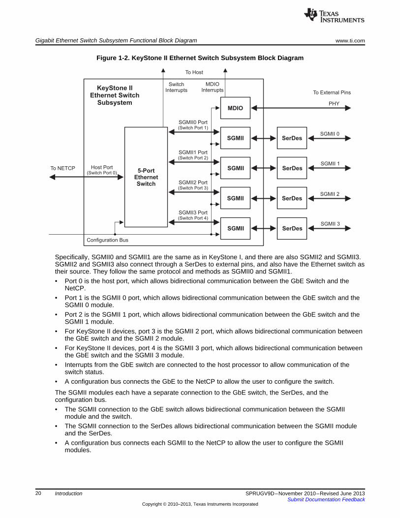
5-PortEthernetSwitch
MDIO
SGMII
SGMII
SGMII0 Port(Switch Port 1)
SGMII1 Port(Switch Port 2)
SerDes
SerDes
Configuration Bus
To External Pins
SGMII 0
SGMII 1
PHY
MDIOInterrupts
SwitchInterrupts
Host Port(Switch Port 0)
KeyStone IIEthernet Switch
Subsystem
To NETCP
To Host
SGMII
SGMII
SGMII2 Port(Switch Port 3)
SGMII3 Port(Switch Port 4)
SerDes
SerDes
SGMII 2
SGMII 3
Gigabit Ethernet Switch Subsystem Functional Block Diagram www.ti.com
20 SPRUGV9D–November 2010–Revised June 2013Submit Documentation Feedback
Copyright © 2010–2013, Texas Instruments Incorporated
Introduction
Figure 1-2. KeyStone II Ethernet Switch Subsystem Block Diagram
Specifically, SGMII0 and SGMII1 are the same as in KeyStone I, and there are also SGMII2 and SGMII3.SGMII2 and SGMII3 also connect through a SerDes to external pins, and also have the Ethernet switch astheir source. They follow the same protocol and methods as SGMII0 and SGMII1.• Port 0 is the host port, which allows bidirectional communication between the GbE Switch and the
NetCP.• Port 1 is the SGMII 0 port, which allows bidirectional communication between the GbE switch and the
SGMII 0 module.• Port 2 is the SGMII 1 port, which allows bidirectional communication between the GbE switch and the
SGMII 1 module.• For KeyStone II devices, port 3 is the SGMII 2 port, which allows bidirectional communication between
the GbE switch and the SGMII 2 module.• For KeyStone II devices, port 4 is the SGMII 3 port, which allows bidirectional communication between
the GbE switch and the SGMII 3 module.• Interrupts from the GbE switch are connected to the host processor to allow communication of the
switch status.• A configuration bus connects the GbE to the NetCP to allow the user to configure the switch.
The SGMII modules each have a separate connection to the GbE switch, the SerDes, and theconfiguration bus.• The SGMII connection to the GbE switch allows bidirectional communication between the SGMII
module and the switch.• The SGMII connection to the SerDes allows bidirectional communication between the SGMII module
and the SerDes.• A configuration bus connects each SGMII to the NetCP to allow the user to configure the SGMII
modules.
www.ti.com Industry Standard(s) Compliance Statement
21SPRUGV9D–November 2010–Revised June 2013Submit Documentation Feedback
Copyright © 2010–2013, Texas Instruments Incorporated
Introduction
The MDIO module, as shown in Figure 1-1, contains a connection to an external PHY device, a set ofinterrupts going to the host, and bus configuration through the network coprocessor.• The connection to an external PHY device allows the MDIO module to monitor the link status of up to
32 addresses.• Interrupts from the MDIO module are connected to the host to allow communication of changes in link
status.• A configuration bus connects the MDIO to the NetCP to allow the user to configure the MDIO.
Note that for KeyStone II devices, there are four instead of two SGMII ports to use, meaning that there arefive ports total. These additional ports have the same functionality as the SGMII ports described above.
1.4 Industry Standard(s) Compliance StatementThe gigabit Ethernet switch subsystem conforms to the following industry standards:• Supports IEEE 802.3 specification• Supports IEEE 1588 specification
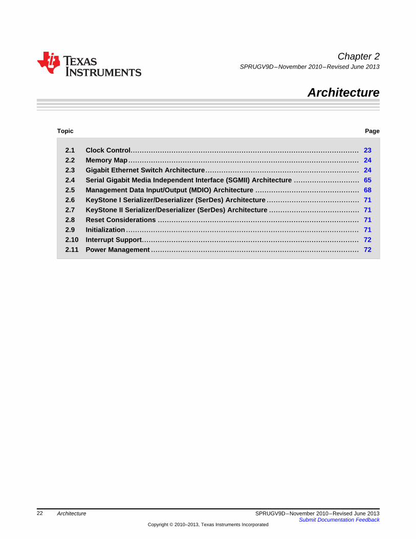
22 SPRUGV9D–November 2010–Revised June 2013Submit Documentation Feedback
Copyright © 2010–2013, Texas Instruments Incorporated
Architecture
Chapter 2SPRUGV9D–November 2010–Revised June 2013
Architecture
Topic ........................................................................................................................... Page
2.1 Clock Control..................................................................................................... 232.2 Memory Map ...................................................................................................... 242.3 Gigabit Ethernet Switch Architecture.................................................................... 242.4 Serial Gigabit Media Independent Interface (SGMII) Architecture ............................. 652.5 Management Data Input/Output (MDIO) Architecture .............................................. 682.6 KeyStone I Serializer/Deserializer (SerDes) Architecture ......................................... 712.7 KeyStone II Serializer/Deserializer (SerDes) Architecture ........................................ 712.8 Reset Considerations ......................................................................................... 712.9 Initialization ....................................................................................................... 712.10 Interrupt Support................................................................................................ 722.11 Power Management ............................................................................................ 72
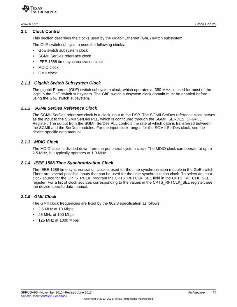
www.ti.com Clock Control
23SPRUGV9D–November 2010–Revised June 2013Submit Documentation Feedback
Copyright © 2010–2013, Texas Instruments Incorporated
Architecture
2.1 Clock ControlThis section describes the clocks used by the gigabit Ethernet (GbE) switch subsystem.
The GbE switch subsystem uses the following clocks:• GbE switch subsystem clock• SGMII SerDes reference clock• IEEE 1588 time synchronization clock• MDIO clock• GMII clock
2.1.1 Gigabit Switch Subsystem ClockThe gigabit Ethernet (GbE) switch subsystem clock, which operates at 350 MHz, is used for most of thelogic in the GbE switch subsystem. The GbE switch subsystem clock domain must be enabled beforeusing the GbE switch subsystem.
2.1.2 SGMII SerDes Reference ClockThe SGMII SerDes reference clock is a clock input to the DSP. The SGMII SerDes reference clock servesas the input to the SGMII SerDes PLL, which is configured through the SGMII_SERDES_CFGPLLRegister. The output from the SGMII SerDes PLL controls the rate at which data is transferred betweenthe SGMII and the SerDes modules. For the input clock ranges for the SGMII SerDes clock, see thedevice-specific data manual.
2.1.3 MDIO ClockThe MDIO clock is divided down from the peripheral system clock. The MDIO clock can operate at up to2.5 MHz, but typically operates at 1.0 MHz.
2.1.4 IEEE 1588 Time Synchronization ClockThe IEEE 1588 time synchronization clock is used for the time synchronization module in the GbE switch.There are several possible inputs that can be used for the time synchronization clock. To select an inputclock source for the CPTS_RCLK, program the CPTS_RFTCLK_SEL field in the CPTS_RFTCLK_SELregister. For a list of clock sources corresponding to the values in the CPTS_RFTCLK_SEL register, seethe device-specific data manual.
2.1.5 GMII ClockThe GMII clock frequencies are fixed by the 802.3 specification as follows:• 2.5 MHz at 10 Mbps• 25 MHz at 100 Mbps• 125 MHz at 1000 Mbps
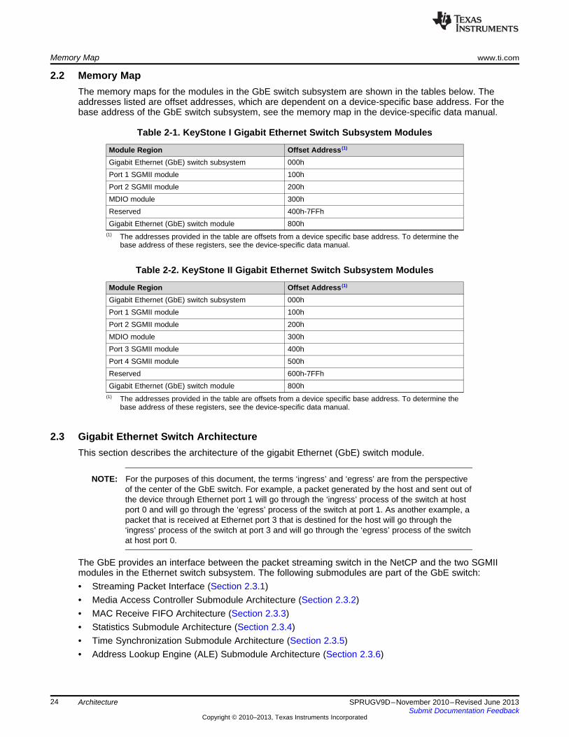
Memory Map www.ti.com
24 SPRUGV9D–November 2010–Revised June 2013Submit Documentation Feedback
Copyright © 2010–2013, Texas Instruments Incorporated
Architecture
2.2 Memory MapThe memory maps for the modules in the GbE switch subsystem are shown in the tables below. Theaddresses listed are offset addresses, which are dependent on a device-specific base address. For thebase address of the GbE switch subsystem, see the memory map in the device-specific data manual.
(1) The addresses provided in the table are offsets from a device specific base address. To determine thebase address of these registers, see the device-specific data manual.
Table 2-1. KeyStone I Gigabit Ethernet Switch Subsystem Modules
Module Region Offset Address (1)
Gigabit Ethernet (GbE) switch subsystem 000hPort 1 SGMII module 100hPort 2 SGMII module 200hMDIO module 300hReserved 400h-7FFhGigabit Ethernet (GbE) switch module 800h
(1) The addresses provided in the table are offsets from a device specific base address. To determine thebase address of these registers, see the device-specific data manual.
Table 2-2. KeyStone II Gigabit Ethernet Switch Subsystem Modules
Module Region Offset Address (1)
Gigabit Ethernet (GbE) switch subsystem 000hPort 1 SGMII module 100hPort 2 SGMII module 200hMDIO module 300hPort 3 SGMII module 400hPort 4 SGMII module 500hReserved 600h-7FFhGigabit Ethernet (GbE) switch module 800h
2.3 Gigabit Ethernet Switch ArchitectureThis section describes the architecture of the gigabit Ethernet (GbE) switch module.
NOTE: For the purposes of this document, the terms ‘ingress’ and ‘egress’ are from the perspectiveof the center of the GbE switch. For example, a packet generated by the host and sent out ofthe device through Ethernet port 1 will go through the ‘ingress’ process of the switch at hostport 0 and will go through the ‘egress’ process of the switch at port 1. As another example, apacket that is received at Ethernet port 3 that is destined for the host will go through the‘ingress’ process of the switch at port 3 and will go through the ‘egress’ process of the switchat host port 0.
The GbE provides an interface between the packet streaming switch in the NetCP and the two SGMIImodules in the Ethernet switch subsystem. The following submodules are part of the GbE switch:• Streaming Packet Interface (Section 2.3.1)• Media Access Controller Submodule Architecture (Section 2.3.2)• MAC Receive FIFO Architecture (Section 2.3.3)• Statistics Submodule Architecture (Section 2.3.4)• Time Synchronization Submodule Architecture (Section 2.3.5)• Address Lookup Engine (ALE) Submodule Architecture (Section 2.3.6)
www.ti.com Gigabit Ethernet Switch Architecture
25SPRUGV9D–November 2010–Revised June 2013Submit Documentation Feedback
Copyright © 2010–2013, Texas Instruments Incorporated
Architecture
The KeyStone I GbE switch has three ports: port 0 communicates with the packet streaming switch, port 1communicates with the SGMII0 module, and port 2 communicates with the SGMII1 module. The KeyStoneII version has two additional ports to the SGMII module, port 3 and port 4. Port 3 communicates with theSGMII3 module and port 4 communicates with the SGMII4 module.
To interface to the packet streaming switch, the GbE switch contains transmit and receive interfaces toconvert between the signals used by the GbE switch and the signals used by the packet streaming switch.To facilitate communication with the SGMII modules, KeyStone I devices have two MAC submodules(EMAC0 and EMAC1) to convert between the signals internal to the switch and the GMII signals requiredby the SGMII modules. KeyStone II devices have two additional MAC submodules (EMAC2 and EMAC3),for a total of four.
The GbE switch also contains several other submodules that provide additional features. The GbE switchhas two modules that provide Ethernet statistics for the packets transmitted and received by the Ethernetswitch subsystem. The GbE switch also contains a time synchronization submodule to support IEEE 1588clock synchronization. The GbE switch provides an address lookup engine (ALE), which is responsible forforwarding and filtering packets based on address. Each of these submodules is covered in more detail inthe respective submodule sections.
2.3.1 Streaming Packet InterfaceThis section describes the details of the streaming packet interface. The streaming packet interface isresponsible for communication between the GbE switch and the packet streaming switch in the NetCP.
For KeyStone I devices, see the Network Coprocessor (NETCP) for KeyStone Devices User's Guide(SPRUGZ6) for definition of the control register for TXA and TXB.
For KeyStone II devices, see the Network Coprocessor (NETCP) for KeyStone Devices User's Guide(SPRUHZ0) for definition of the control register for TXA, TXB, TXC, and TXD. Note that TXC and TXD areavailable only in KeyStone II devices with the 5-port switch.
2.3.1.1 Transmit Streaming Packet InterfaceThe transmit interface is responsible for transmitting packets from the GbE switch port 0 to the packetstreaming switch in the NETCP. The GbE switch has two identical transmit streaming packet interfaces.The first interface (TXA) outputs packets received on port 1 that are destined for port 0. The secondinterface (TXB) outputs packets that were received on port 2 and are destined for port 0. The data on thestreaming interface data is equivalent to MAC output data with the difference being that instead ofoutputting 8-bit GMII data, the data output is formatted for transmission on the streaming interface.
In addition to the packet data, the transmit streaming interface also provides additional information that isplaced in the descriptor of the received packet by the receive flow of the packet DMA. Included in thisextra information is source identification. If the packet originated from port 1, then the value in theTXA_SRC_ID field of the P0_CPPI_SRC_ID Register will be placed in SRC_ID field in the descriptor ofthe receive packet. Similarly, if the packet originated from port 2, the value in the TXB_SRC_ID field of theP0_CPPI_SRC_ID Register is placed in the SRC_ID field in the receive packet descriptor.
Both TXA and TXB transmit interfaces have a 22K-byte buffer to enable more efficient transmit packetoperations. The transmit interfaces do not transmit packets on the streaming interface until there is anentire packet in the output buffer or until there is at least CPPI_THRESH plus two words (not bytes) in theoutput buffer. The plus two is there because a two-word double buffer is also present.
For KeyStone II, additional ports TXC and TXD are included with functionality identical to the TXA andTXB interfaces.
2.3.1.1.1 Transmit VLAN ProcessingThis section covers transmit processing when in VLAN-aware mode. The GbE switch is in VLAN-awaremode when the VLAN_AWARE bit is set in the CPSW_CONTROL Register and the ALE_VLAN_AWAREbit is set in the ALE_CONTROL register. While in VLAN-aware mode, VLAN is added, removed, orreplaced according to the same rules as the MAC transmit (egress) output packet VLAN process.Transmit packets are not modified when VLAN_AWARE is cleared to 0.
Gigabit Ethernet Switch Architecture www.ti.com
26 SPRUGV9D–November 2010–Revised June 2013Submit Documentation Feedback
Copyright © 2010–2013, Texas Instruments Incorporated
Architecture
2.3.1.2 Receive Streaming Packet InterfaceThe receive streaming interface on port 0 of the GbE switch is responsible for receiving packets from thepacket streaming switch in the NetCP. The GbE switch has one receive streaming packet interface for port0. The CPPI receive port is equivalent to a MAC port with the difference being that the data is provided tothe GbE switch in the streaming interface data format instead of 8-bit GMII data format.
In addition to the packet data, the receive streaming interface can also provide additional controlinformation that resides in the PS_FLAGS field of the descriptor of the packet that was transmitted to theGbE switch.
For packets being transmitted to the GbE, the PS_FLAGS field has the following configuration:
Table 2-3. KeyStone I PS_FLAGS for GbE Switch Ingress Packets
PS_FLAGSBits Field Description3 RX_PASS_CRC Receive pass CRC.
• 0 = The packet does not contain a CRC. The CRC should be generated by the MAC module.• 1 = The packet already contains a CRC. The CRC should not be generated by the MAC module.
2-0 TO_PORT Directed packet to port. Setting these bits to a non-zero value indicates that the packet is a directedpacket. Packets with the these bits set will bypass the ALE and send the packet directly to the portindicated.• 0 = No effect• 1 = Send packet to GbE switch port 1• 2 = Send packet to GbE switch port 2• 3-7 = Reserved
Table 2-4. KeyStone II PS_FLAGS for GbE Switch Ingress Packets
PS_FLAGSBits Field Description3 RX_PASS_CRC Receive pass CRC.
• 0 = The packet does not contain a CRC. The CRC should be generated by the MAC module.• 1 = The packet already contains a CRC. The CRC should not be generated by the MAC module.
2-0 TO_PORT Directed packet to port. Setting these bits to a non-zero value indicates that the packet is a directedpacket. Packets with the these bits set bypass the ALE and send the packet directly to the portindicated.• 0 = No effect• 1 = Send packet to GbE switch port 1• 2 = Send packet to GbE switch port 2• 3 = Send packet to GbE switch port 3• 4 = Send packet to GbE switch port 4• Others = Reserved
Setting the RX_PASS_CRC bit indicates that the CRC is passed with the packet data. The packet is adirected packet when any of the TO_PORT bits are non-zero. The packet will be sent to the port indicated.A packet may only be directed to a single port. For directed packets the destination lookup process in theALE is skipped. However, in VLAN aware mode (VLAN_AWARE bit set to 1 in the CPSW_CONTROLregister and ALE_VLAN_AWARE set to 1 in the ALE_CONTROL register) the lookup still takes place butonly to determine if the packet should have the VLAN tag removed during egress (forced untaggedegress).
www.ti.com Gigabit Ethernet Switch Architecture
27SPRUGV9D–November 2010–Revised June 2013Submit Documentation Feedback
Copyright © 2010–2013, Texas Instruments Incorporated
Architecture
2.3.2 Media Access Controller Submodule ArchitectureThis section describes the architecture of the media-access-controller (MAC) submodule. The MACsubmodule is IEEE 802.3 compliant and supports 10/100/1000 megabit per second (Mbps) modes ofoperation. The MAC module provides an interface between the GbE switch and the SGMII modules. Fortransmit operations, the MAC module converts between data signals used by the GbE switch and GMIIsignals used by the SGMII modules. For receive operations, the MAC module converts between GMIIsignals from the SGMII module to the signals used by the GbE switch. Transmit and receive operationsare described in more detail in subsequent sections.
In addition to translating between the SGMII modules and the GbE switch, the MAC module is responsiblefor operations related to IEEE 802.3 Ethernet frames. For all packets, the MAC module adds or removesthe preamble, start of frame delimiter, and interpacket gap to a packet. The MAC module verifies andoptionally generates CRC checksums.
2.3.2.1 Data Receive OperationsThis section describes the data-receive operations of the MAC module.
2.3.2.1.1 Receive ControlThe MAC module is responsible for interpreting GMII data received from the SGMII module. Interpretationof GMII data involves the following operations:• Detection and removal of the preamble• Detection and removal of the start-of-frame delimiter• Extraction of the address• Extraction of the frame length• Data handling• Error checking and reporting• Cyclic redundancy checking (CRC)• Statistics signal generation
All statistics signal generation is reported to the proper statistics module in the GbE switch.
2.3.2.1.2 Receive Interframe IntervalThe 802.3 required interpacket gap (IPG) is 24 GMII clocks (96 bit times) for 10/100 Mbps modes, and 12GMII clocks (96 bit times) for 1000 Mbps mode. However, the MAC module can tolerate a reduced IPG (2GMII clocks in 10/100 mode and 5 GMII clocks in 1000 mode) with a correct preamble and start of framedelimiter.
This interval between frames must include (in the following order):1. An interpacket gap (IPG)2. A seven-octet preamble (all octets 0x55)3. A one-octet start of frame delimiter (0x5D)
2.3.2.1.3 Receive Flow ControlThis section describes the receive flow control functionality. When under heavy load, the MAC module canlimit further frame reception through receive frame flow control. Receive flow control is enabled by settingthe RX_FLOW_EN bit in the MAC_CONTROL Register. When enabled, flow control events are triggeredby the receive FIFO in the GbE switch module. When receive flow control is enabled, and a flow controlevent is triggered, receive flow control is initiated. When in half-duplex mode, receive flow control iscollision based. While in full duplex mode, flow control is handled by issuing 802.3X pause frames. Ineither case, receive flow control prevents frame reception by issuing the flow control appropriate for thecurrent mode of operation. The MAC module is configured for collision or IEEE 802.3X flow control via theFULLDUPLEX bit in the MAC_CONTROL Register.
Gigabit Ethernet Switch Architecture www.ti.com
28 SPRUGV9D–November 2010–Revised June 2013Submit Documentation Feedback
Copyright © 2010–2013, Texas Instruments Incorporated
Architecture
2.3.2.1.3.1 Collision Based Receive Flow ControlCollision-based receive flow control provides a means of preventing frame reception when the port isoperating in half-duplex mode (the FULLDUPLEX bit is cleared in the MAC_CONTROL register). Whenreceive flow control is enabled and triggered, the port generates collisions for received frames. The jamsequence transmitted is the twelve-byte sequence C3.C3.C3.C3.C3.C3.C3.C3.C3.C3.C3.C3 (hex). Thejam sequence begins no later than the moment the source address begins to be received. Note that theseforced collisions are not limited to a maximum of 16 consecutive collisions and are independent of thenormal back-off algorithm. Receive flow control does not depend on the value of the incoming framedestination address. A collision is generated for any incoming packet, regardless of the destinationaddress.
2.3.2.1.3.2 IEEE 802.3X Based Receive Flow ControlIEEE 802.3x-based receive flow control provides a means of preventing frame reception when the port isoperating in full-duplex mode (the FULLDUPLEX bit is set in MAC_CONTROL register). When receiveflow control is enabled and triggered, the port transmits a pause frame to request that the sending stationstop transmitting for the period indicated within the transmitted pause frame.
The MAC module transmits a pause frame to the reserved multicast address at the first availableopportunity. If the MAC module is idle, a pause frame is transmitted immediately, otherwise the pauseframe is sent following the completion of the frame currently being transmitted. When issuing a pauseframe, the frame contains 0xFFFF, which is the maximum possible pause time value. The MAC modulecounts the receive pause frame time, decrementing 0xFF00 down to 0, and retransmits an outgoing pauseframe if the count reaches 0. When the flow control request is removed, the MAC module transmits apause frame with a zero pause time to cancel the pause request.
NOTE: Transmitted pause frames are only a request to the other end station to stop transmitting.Frames that are received during the pause interval are received normally (provided thereceive FIFO is not full).
Pause frames are transmitted if enabled and triggered regardless of whether the port is observing thepause time period from an incoming pause frame.
The MAC module transmits pause frames as described below:• The 48-bit reserved multicast destination address 01.80.C2.00.00.01• The 48-bit source address found in the SLx_SA_HI and SLx_SA_LO Registers in the GbE switch• The 16-bit length/type field containing the value 88.08• The 16-bit pause opcode equal to 00.01• The 16-bit pause time value FF.FF. A pause-quantum is 512 bit-times. Pause frames sent to cancel a
pause request will have a pause time value of 00.00.• Zero padding to 64-byte data length (The MAC module will transmit only 64-byte pause frames)• The 32-bit frame-check sequence (CRC word)
All quantities above are hexadecimal and are transmitted most-significant byte first. The least-significantbit is transferred first in each byte.
If RX_FLOW_EN is cleared to 0 while the pause time is non-0, the pause time will be cleared to 0, and a0-count pause frame will be sent.
2.3.2.2 Data TransmissionThis section describes transmit data operations for the MAC module. The MAC module accepts data fromthe GbE switch, converts the data to GMII format, and transmits the data to the SGMII module. Datatransmission is synchronized to the transmit clock rate. The smallest frame that can be sent is two bytesof data with four bytes of CRC (6 byte frame).
www.ti.com Gigabit Ethernet Switch Architecture
29SPRUGV9D–November 2010–Revised June 2013Submit Documentation Feedback
Copyright © 2010–2013, Texas Instruments Incorporated
Architecture
2.3.2.2.1 Transmit ControlThis section describes transmit control operations for the MAC module. If a collision is detected on atransmit packet , the MAC module outputs a jam sequence. If the collision was late (after the first 64 byteshave been transmitted) the collision is ignored. If the collision is not late, the controller will back off beforeretrying the frame transmission. When operating in full duplex mode, the carrier sense (CRS) and collisionsensing modes are disabled.
2.3.2.2.2 CRC InsertionThis section describes the procedure for inserting CRC checksums into Ethernet frames. The MACmodule can generate and append a 32-bit Ethernet CRC onto transmitted data. By default, the MACmodule generates and appends a CRC. If the user does not want the MAC module to generate a CRC, bit19 of the protocol-specific flags region of the descriptor must be set before transmitting the packet via thepacket DMA to the NETCP. If bit 19 of the protocol-specific flags is set in the descriptor, the last four bytesof the TX data are transmitted as the frame CRC. The four CRC data bytes should be the last four bytesof the frame and should be included in the packet byte count value. The MAC performs no error checkingon the outgoing CRC when bit 19 of the protocol-specific flags field is set in the descriptor.
NOTE: The protocol-specific flags field of a descriptor is a general purpose region used to pass datato the module to which the descriptor is being transmitted. Each module interprets the bitpattern in the protocol-specific flags regions differently. Therefore, the user should set onlybit 19 in the protocol-specific flags field to bypass the CRC checksum when sending thepacket directly to the GbE switch through the queue manager subsystem. If the packet issent to another module such as the Packet Accelerator (PA) (to complete a task such as aUDP checksum), or to the Security Accelerator (SA) (to perform a task such as encryption),before sending the packet to the GbE switch, setting bit 19 in the protocol-specific field willresult in undefined behavior.
2.3.2.2.3 MTXERThe GMII MTXER signal is not used in the MAC module. If an underflow condition occurs on a transmittedframe, the frame CRC will be inverted to indicate the error to the network. Underflow is a hardware error.
2.3.2.2.4 Adaptive Performance Optimization (APO)This section describes adaptive performance optimization (APO) implemented in the MAC module. TheEthernet MAC port incorporates APO logic that may be enabled by setting the TX_PACE bit in theMAC_CONTROL register. When the TX_PACE bit is set, transmission pacing to enhance performance isenabled. Adaptive performance pacing introduces delays into the normal transmission of frames, delayingtransmission attempts between stations. By introducing delays, the probability of collisions will be reducedduring heavy traffic (as indicated by frame deferrals and collisions), thereby increasing the chance ofsuccessful transmission.
When a frame is deferred, suffers a single collision, multiple collisions, or excessive collisions, the pacingcounter is loaded with an initial value of 31. When a frame is transmitted successfully (withoutexperiencing a deferral, single collision, multiple collision, or excessive collision) the pacing counter isdecremented by 1, down to 0.
With pacing enabled, a new frame is permitted to immediately (after one IPG) attempt transmission only ifthe pacing counter is 0. If the pacing counter is non-0, the frame is delayed by the pacing delay, which isequivalent to approximately four Interpacket gap delays. APO affects only the IPG preceding the firstattempt at transmitting a frame. It does not affect the back-off algorithm for retransmitted frames.
Gigabit Ethernet Switch Architecture www.ti.com
30 SPRUGV9D–November 2010–Revised June 2013Submit Documentation Feedback
Copyright © 2010–2013, Texas Instruments Incorporated
Architecture
2.3.2.2.5 Interpacket Gap EnforcementThis section describes the enforcement of interpacket gap for the MAC module. The measurementreference for the IPG of 96 bit times is changed depending on frame traffic conditions. If a frame issuccessfully transmitted without collision, and the MCRS signal is deasserted within approximately 48 bittimes of the MTXEN signal being deasserted, 96 bit times is measured from MTXEN. If the frame suffereda collision, or if the MCRS signal is not de-asserted until more than approximately 48 bit times afterMTXEN is deasserted, 96 bit times (approximately, but not less) is measured from MCRS.
The transmit IPG can be shortened by eight bit times when enabled and triggered. TheTX_SHORT_GAP_EN bit in the MAC_CONTROL register enables the TX_SHORT_GAP input todetermine whether the transmit IPG is shorted by eight bit times.
2.3.2.2.6 Back OffThe MAC module implements the 802.3 binary exponential back-off algorithm .
2.3.2.2.7 Programmable Transmit Interpacket GapThe transmit interpacket gap (IPG) is programmable through the TX_GAP register. The default value isdecimal 12. The transmit IPG may be increased to the maximum value of 0x1ff. Increasing the IPG is notcompatible with transmit pacing. The short gap feature will override the increased gap value, so the shortgap feature may not be compatible with an increased IPG.
2.3.2.2.8 Transmit Flow ControlThis section describes the IEEE 802.3X based transmit flow control implemented in the MAC module.When enabled, incoming pause frames are acted upon to prevent the MAC module from transmitting anyfurther frames. Incoming pause frames are acted upon only when the FULLDUPLEX and TX_FLOW_ENbits are set in the MACCONTROL Register. Pause frames are not acted upon in half-duplex mode. Pauseframe action will be taken if enabled, but normally the frame will be filtered and not transferred to memory.MAC control frames will be transferred to memory if the RX_CMF_EN (copy MAC Frames) bit in theMAC_CONTROL Register is set. The TX_FLOW_EN and FULLDUPLEX bits effect whether or not MACcontrol frames are acted upon, but they have no effect upon whether or not MAC control frames aretransferred to memory or filtered.
Pause frames are a subset of MAC control frames with an opcode field=0x0001. Incoming pause frameswill be acted upon by the port only if all the following conditions are met:• TX_FLOW_EN is set in the MAC_CONTROL Pn_MAC_CTL register• The frame’s length is 64 to MAC_RX_MAXLEN RX_MAXLEN bytes inclusive• The frame contains no CRC error or align/code errors
The pause-time value from valid frames is extracted from the two bytes following the opcode. The pausetime will be loaded into the port’s transmit pause timer and the transmit pause time period will begin.
www.ti.com Gigabit Ethernet Switch Architecture
31SPRUGV9D–November 2010–Revised June 2013Submit Documentation Feedback
Copyright © 2010–2013, Texas Instruments Incorporated
Architecture
If a valid pause frame is received during the transmit pause time period of a previous transmit pauseframe then:• If the destination address is not equal to the reserved multicast address or any enabled or disabled
unicast address, then the transmit pause timer will immediately expire, or• If the new pause time value is 0, then the transmit pause timer will immediately expire, else• The port transmit pause timer will immediately be set to the new pause frame pause time value. (Any
remaining pause time from the previous pause frame will be discarded.)
If the TX_FLOW_EN field in the MAC_CONTROL Pn_MAC_CTL register is cleared, then the pause-timerwill immediately expire.
The port will not start the transmission of a new data frame any sooner than 512-bit times after a pauseframe with a non-zero pause time has finished being received (MRXDV going inactive). No transmissionwill begin until the pause timer has expired (the port may transmit pause frames in order to initiateoutgoing flow control). Any frame already in transmission when a pause frame is received will becompleted and unaffected.
Incoming pause frames consist of:• A 48-bit destination address equal to:
– The reserved multicast destination address 01.80.C2.00.00.01, or– The 48-bit MAC source address found in the SLx_SA_HI and SLx_SA_LO Registers in the GbE
switch• The 48-bit source address of the transmitting device• The 16-bit length/type field containing the value 88.08• The 16-bit pause opcode equal to 00.01• The 16-bit pause_time. A pause-quantum is 512 bit-times• Padding to 64-byte data length• The 32-bit frame-check sequence (CRC word)
All quantities above are hexadecimal and are transmitted most-significant byte first. The least-significantbit is transferred first in each byte.
The padding is required to make up the frame to a minimum of 64 bytes. The standard allows pauseframes longer than 64 bytes to be discarded or interpreted as valid pause frames. The MAC module willrecognize any pause frame between 64 bytes and MAC_RX_MAXLENRX_MAXLEN bytes in length.
2.3.2.2.9 Speed, Duplex Mode, and Pause Frame Support NegotiationThe MAC module can operate in half duplex or full duplex in 10/100 Mbps modes, and can operate only infull duplex in 1000 Mbps mode. Pause frame support is included in 10/100/1000 Mbps modes asconfigured by the host.
2.3.2.2.10 Frame ClassificationReceived frames are proper (good) frames if they are between 64 and MAC_RX_MAXLEN in length(inclusive) and contain no errors (code/align/CRC).
Received frames are long frames if their frame count exceeds the value in the MAC_RX_MAXLENregister. The default MAC_RX_MAXLEN register value is 1518 (decimal). Long received frames are eitheroversized or jabber frames. Long frames with no errors are oversized frames. Long frames with CRC,code, or alignment errors are jabber frames.
Received frames are short frames if their frame count is less than 64 bytes. Short frames that contain noerrors are undersized frames. Short frames with CRC, code, or alignment errors are fragment frames.
Gigabit Ethernet Switch Architecture www.ti.com
32 SPRUGV9D–November 2010–Revised June 2013Submit Documentation Feedback
Copyright © 2010–2013, Texas Instruments Incorporated
Architecture
A received long packet will always contain MAC_RX_MAXLEN number of bytes transferred to memory (ifRX_CEF_EN = 1). An example with MAC_RX_MAXLEN = 1518 is below:• If the frame length is 1518, then the packet is not a long packet and there will be 1518 bytes
transferred to memory• If the frame length is 1519, there will be 1518 bytes transferred to memory. The last three bytes will be
the first three CRC bytes• If the frame length is 1520, there will be 1518 bytes transferred to memory. The last two bytes will be
the first two CRC bytes• If the frame length is 1521, there will be 1518 bytes transferred to memory. The last byte will be the
first CRC byte• If the frame length is 1522, there will be 1518 bytes transferred to memory. The last byte will be the
last data byte
2.3.3 MAC Receive FIFO ArchitectureThis section describes the architecture of the MAC receive FIFOs. Internal to the GbE switch, both MACports have an identical packet FIFO. Each packet FIFO contains a single logical receive queue and fourlogical transmit queues (priority 0 through 3). Each packet FIFO memory contains 81,920 bytes (80k) totalorganized as 10240 by 64-bit words contained in a single memory instance. The packet FIFO memory isused for the associated port transmit and receive queues. The TX_MAX_BLKS field in the FIFO’sassociated MAX_BLKS Register determines the maximum number of 4k FIFO memory blocks to beallocated to the four logical transmit queues (transmit total). The RX_MAX_BLKS field in the FIFO’sassociated MAX_BLKS Register determines the maximum number of 4k memory blocks to be allocated tothe logical receive queue. The TX_MAX_BLKS value plus the RX_MAX_BLKS value should sum to 20(the total number of blocks in the FIFO). If the sum were less than 20 then some memory blocks would beunused. The default is 17 (decimal) transmit blocks and three receive blocks for a port that does not haveflow control enabled. When a port is configured for flow control mode, the receive FIFO blocks allocationshould be increased with a corresponding decrease in transmit FIFO blocks.
www.ti.com Gigabit Ethernet Switch Architecture
33SPRUGV9D–November 2010–Revised June 2013Submit Documentation Feedback
Copyright © 2010–2013, Texas Instruments Incorporated
Architecture
2.3.4 Statistics Submodule ArchitectureThis section describes the architecture of the statistics modules in the GbE switch (see Section 3.5.4.)
The GbE switch has two sets of statistics modules that record events associated with packets enteringand exiting the switch. The statistics for KeyStone I switch port 0 are recorded on statistics module A(STATSA), and statistics for ports 1 and 2 are recorded on statistics module B (STATSB). For KeyStone IIdevices, the additional ports are recorded in the additional statistics modules STATSC and STATSD. Eachstatistic register is 32-bits wide and automatically increments when a certain statistics condition is met.Each statistic will rollover from 0xFFFFFFFF to 0x00000000.
For Keystone II, the Ethernet switch has four sets of statistics that record events associated with frametraffic on selected switch ports. STATSA keeps statistics for port 0 receive, port 0 TXA, and port 0 TXB.STATSC keeps statistics for port 0 TXC and port 0 TXD (STATSC receive statistics are unused). STATSBkeeps statistics for port 1 and STATSD keeps statistics for ports 3 and 4. The statistics are paged in theaddress map. STATSA/B statistics are visible in the address range when stat_sel is cleared to 0 in theStat_Port Register. STATSC/D statistics are visible in the address range when stat_sel is set to 1 in theStat_Port Register.
NOTE: To view the STATS for the STATS module, they must first be enabled in the StatsConfiguration Register.
KeyStone I devices have only STATSA and STATSB — no STATSC or STATSD.
KeyStone II devices have STATSA and STATSB, plus STATSC and STATSD. STATSA andSTATSC share the same address space, and STATSB and STATSD share the sameaddress space.
The user must configure the STATS enable register (Statics port Enable RegisterSTAT_PORT_EN -- Section 3.5.1.4) to pick which of the pair of STATS modules to view —either STATSA/STATSB for port 0 and port 1, or STATSC/STATSD for port 2 and port 3. Allfour cannot be viewed at the same time because they share the same address space.
2.3.4.1 Accessing Statistics RegistersThis section describes how to correctly read and write to the registers in the statistics modules while themodules are disabled or enabled. By default, the statistics modules are disabled. While disabled, allstatistics registers can be read and written normally, so writing 0x00000000 clears a statistics register.After the statistics modules are enabled, all statistics can still be read normally; however, register writeswill become write to decrement, meaning that the value written to the register will be subtracted from theregister value, with the result being stored in the register (new register value = old register value - writevalue). If the value written is greater than the value in the statistics register, then 0 will be written to thatregister. When a statistics module is enabled, writing a value of 0xFFFFFFFF will clear a statisticslocation. When writing to a statistics register, 32-bit accesses must be used. The statistics modules can beenabled by writing to bits 3:0 the STAT_PORT_EN Register.
2.3.4.2 Statistics InterruptsThis section describes interrupts generated by the statistics modules. For KeyStone I, each of the twostatistics modules have the ability to send an interrupt to the host. The interrupt for the STATSA modulewill occur on the STAT_PEND_RAW[0] signal, and the interrupt for the STATSB module will occur on theSTAT_PEND_RAW[1] signal. The interrupt will be triggered when any of the values in the statisticsregisters become greater than or equal to 0x80000000. The statistics interrupt can be removed by writinga value greater than 0x80000000.
For KeyStone II devices, STAT_PEND_RAW is a 4-bit value, with the third and fourth bit representingSTATSC and STATSD respectively.
Gigabit Ethernet Switch Architecture www.ti.com
34 SPRUGV9D–November 2010–Revised June 2013Submit Documentation Feedback
Copyright © 2010–2013, Texas Instruments Incorporated
Architecture
2.3.4.3 Receive Statistics Descriptions
2.3.4.3.1 Good Receive FramesThe good receive frames statistic is the total number of good frames received on the port. A good framehas the following characteristics:• Any data or MAC control frame that matched a unicast, broadcast, or multicast address, or matched
due to promiscuous mode• Was of length 64 to RX_MAXLEN bytes inclusive• Had no CRC error, alignment error, or code error
See the receive align/code errors and receive CRC errors statistic descriptions for definitions of alignment,code, and CRC errors. Overruns have no effect on this statistic.
2.3.4.3.2 Broadcast Receive FramesThe broadcast receive frames statistic is the total number of good broadcast frames received on the port.A good broadcast frame has the following characteristics:• Any data or MAC control frame that was destined for address 0xFFFFFFFFFFFF only• Was of length 64 to RX_MAXLEN bytes inclusive• Had no CRC error, alignment error, or code error
See the receive align/code errors and receive CRC errors statistic descriptions for definitions of alignment,code, and CRC errors. Overruns have no effect on this statistic.
2.3.4.3.3 Multicast Receive FramesThe multicast receive frames statistic is total number of good multicast frames received on the port. Agood multicast frame has the following characteristics:• Any data or MAC control frame that was destined for any multicast address other than
0xFFFFFFFFFFFF• Was of length 64 to RX_MAXLEN bytes inclusive• Had no CRC error, alignment error, or code error
See the receive align/code errors and receive CRC errors statistic descriptions for definitions of alignment,code, and CRC errors. Overruns have no effect on this statistic.
2.3.4.3.4 Pause Receive FramesThe pause receive frames statistic is the total number of IEEE 802.3X pause frames received by the port(whether acted upon or not). Such a frame has the following characteristics:• Contained any unicast, broadcast, or multicast address• Contained the length/type field value 88.08 (hex) and the opcode 0x0001• Was of length 64 to RX_MAXLEN bytes inclusive• Had no CRC error, alignment error or code error• Pause-frames had been enabled in the MAC module on that port (TX_FLOW_EN = 1 )
The port could have been in either half-duplex or full-duplex mode.
See the receive align/code errors and receive CRC errors statistic descriptions for definitions of alignment,code and CRC errors. Overruns have no effect on this statistic.
www.ti.com Gigabit Ethernet Switch Architecture
35SPRUGV9D–November 2010–Revised June 2013Submit Documentation Feedback
Copyright © 2010–2013, Texas Instruments Incorporated
Architecture
2.3.4.3.5 Receive CRC ErrorsThe receive CRC errors statistic is the total number of frames received on the port that experienced aCRC error. Such a frame has the following characteristics:• Was any data or MAC control frame that matched a unicast, broadcast, or multicast address, or
matched due to promiscuous mode• Was of length 64 to RX_MAXLEN bytes inclusive• Had no code/align error, and• Had a CRC error
Overruns have no effect on this statistic.
A CRC error has the following characteristics:• A frame containing an even number of nibbles• Fails the frame check sequence test
2.3.4.3.6 Receive Align/Code ErrorsThe receive align/code errors statistic is the total number of frames received on the port that experiencedan alignment error or code error. Such a frame has the following characteristics:• Was any data or MAC control frame that matched a unicast, broadcast. or multicast address, or
matched due to promiscuous mode• Was of length 64 to RX_MAXLEN bytes inclusive• Had either an alignment error or a code error
Over-runs have no effect on this statistic.
An alignment error has the following characteristics:• A frame containing an odd number of nibbles• Fails the frame check sequence test if the final nibble is ignored
A code error is defined to be a frame that has been discarded because the port’s MRXER pin driven witha 1 for at least one bit-time’s duration at any point during the frame’s reception.
NOTE: RFC 1757 etherStatsCRCAlignErrors Ref. 1.5 can be calculated by summing the receivealign/code errors and receive CRC errors (see above).
2.3.4.3.7 Oversize Receive FramesThe oversize receive frames statistic is total number of oversized frames received on the port. Anoversized frame has the following characteristics:• Was any data or MAC control frame that matched a unicast, broadcast, or multicast address, or
matched due to promiscuous mode• Was greater than RX_MAXLEN in bytes• Had no CRC error, alignment error, or code error
See the receive align/code errors and receive CRC errors statistic descriptions for definitions of alignment,code, and CRC errors. Overruns have no effect on this statistic.
Gigabit Ethernet Switch Architecture www.ti.com
36 SPRUGV9D–November 2010–Revised June 2013Submit Documentation Feedback
Copyright © 2010–2013, Texas Instruments Incorporated
Architecture
2.3.4.3.8 Receive Jabber FramesThe receive jabber frames statistic is the total number of jabber frames received on the port. A jabberframe has the following characteristics:• Was any data or MAC control frame that matched a unicast, broadcast, or multicast address, or
matched due to promiscuous mode• Was more than RX_MAXLEN bytes long• Had a CRC error, an alignment error, or a code error
See the receive align/code errors and receive CRC errors statistic descriptions for definitions of alignment,code, and CRC errors. Overruns have no effect on this statistic.
2.3.4.3.9 Undersize (Short) Receive FramesThe undersize receive frames statistic is the total number of undersized frames received on the port. Anundersized frame has the following characteristics:• Any data frame that matched a unicast, broadcast, or multicast address, or matched due to
promiscuous mode• Was less than 64 bytes long• Had no CRC error, alignment error, or code error
See the receive align/code errors and receive CRC errors statistic descriptions for definitions of alignment,code, and CRC errors. Overruns have no effect on this statistic.
2.3.4.3.10 Receive FragmentsThe receive fragments statistic is the total number of frame fragments received on the port. A framefragment has the following characteristics:• Any data frame (address matching does not matter)• Was less than 64 bytes long• Had a CRC error, an alignment error, or a code error• Was not the result of a collision caused by half duplex, collision based flow control
See the receive align/code errors and receive CRC errors statistic descriptions for definitions of alignment,code, and CRC errors. Overruns have no effect on this statistic.
2.3.4.3.11 Receive Start of Frame OverrunsThe receive start of frame overruns statistic is the total number of frames received on the port that had astart of frame (SOF) overrun or were dropped by due to FIFO resource limitations. SOF overrun frame hasthe following characteristics:• Was any data or MAC control frame that matched a unicast, broadcast or multicast address, or
matched due to promiscuous mode• Was any length (including <64 bytes and > RX_MAXLEN bytes)• The packet was dropped due to FIFO resource limitations
www.ti.com Gigabit Ethernet Switch Architecture
37SPRUGV9D–November 2010–Revised June 2013Submit Documentation Feedback
Copyright © 2010–2013, Texas Instruments Incorporated
Architecture
2.3.4.3.12 KeyStone I Overrun Type 1This section describes the overrun type 1 statistic. The overrun type 1 statistic represents a different eventdepending on whether the statistic is recorded in the STATSA or the STATSB module. The STATSAoverrun type 2 and the STATSB overrun type 2 are discussed separately.
In the STATSA module, the overrun type 1 statistic records the total number of frames received on port 0that had a START of frame (SOF) overrun and were dropped on port 0 ingress (port 0 receive FIFO). AnSOF overrun frame has the following characteristics:• Any data or MAC control frame that matched a unicast, broadcast, or multicast address, or matched
due to promiscuous mode• Was any length (including shorter than 64 bytes or longer than RX_MAXLEN bytes)• Had a SOF of frame overrun on port 0.
In the STATSB module, the overrun type 1 statistic records the total number of frames received on port 1or port 2 that had a START of frame (SOF) overrun and were dropped on port 1 or port 2 ingress (port 1or port 2 receive FIFO). An SOF overrun frame has the following characteristics:• Any data or MAC control frame that matched a unicast, broadcast, or multicast address, or matched
due to promiscuous mode• Was any length (including shorter than 64 bytes or longer than RX_MAXLEN bytes)• Had a SOF of frame overrun
2.3.4.3.13 KeyStone II Overrun Type 1In addition to STATSA and STATSB modules, the KeyStone II devices have two addition statisticsmodules STATSC and STATSD.
In the STATSC module, this overrun type is unused. For STATSD, the total number of frames received onport 3 or port 4 that had a SOF overrun and were dropped on port 3 or port 4 ingress (port 3 or port 4FIFO). The SOF overrun frame is defined to be:• Any data of MAC control frame that matched a unicast, broadcast, of multicast address, or matched
due to promiscuous mode• Was any length (including < 64 bytes and > RX_MAXLEN bytes)• Had a SOF of frame overrun
2.3.4.3.14 KeyStone I Overrun Type 2This section describes the overrun type 2 statistic. The overrun type 2 statistic represents a different eventdepending on whether the statistic is recorded in the STATSA or the STATSB module. The STATSAoverrun type 2 and the STATSB overrun type 2 are discussed separately.
In the STATSA module, the overrun type 2 statistic records the total number of frames received on ports 1or 2 that had a middle of frame (MOF) overrun or start of frame (SOF) overrun on CPPI (port 0) egress.An MOF/SOF overrun frame has the following characteristics:• Any data or MAC control frame that matched a unicast, broadcast, or multicast address, or matched
due to promiscuous mode• Was any length (including shorter than 64 bytes or longer than RX_MAXLEN bytes)• Had a MOF/SOF overrun on egress
In the STATSB module, the overrun type 2 statistic records the total number of frames received on port 2that had a start of frame (SOF) overrun on port 1. If KeyStone II, this is for port 1, 2, or 4) egress (whenattempting to load the packet into the port 1 transmit FIFO). An SOF overrun frame has the followingcharacteristics:• Any data or MAC control frame that matched a unicast, broadcast, or multicast address, or matched
due to promiscuous mode• Was any length (including shorter than 64 bytes or longer than RX_MAXLEN bytes)• Had a SOF of frame overrun on port 1 egress
Gigabit Ethernet Switch Architecture www.ti.com
38 SPRUGV9D–November 2010–Revised June 2013Submit Documentation Feedback
Copyright © 2010–2013, Texas Instruments Incorporated
Architecture
2.3.4.3.15 KeyStone II Overrun Type 2For KeyStone II, STATSA and STATSB are the same statistics block as in KeyStone I.
For STATSC, the total number of frames received SOF or Middle of Frame (MOF) on CPPI (port 0)egress. SOF or MOF overrun frame is defined to be:• Any data of control frame that matched a unicast, broadcast or multicast address or matched due to
promiscuous mode• Was any length (including shorter than 64 bytes or longer than RX_MAXLEN bytes)• Has a MOF/SOF overrun on egress
For STATSD, it is the total number of frames received on port 4 that had a SOF overrun on port 1, 2, or 3egress (when attempting to load the packet into the Ethernet port transmit IFIFO). SOF overrun frame isdefined to be:• Any data of control frame that matched a unicast, broadcast or multicast address or matched due to
promiscuous mode• Was any length (including shorter than 64 bytes or longer than RX_MAXLEN bytes)• Has a SOF overrun on port 1 egress.
Note, this stat can under count dropped frames in rare conditions when port 1 and port 2 are on the sameclock.
2.3.4.3.16 Overrun Type 3This section describes the overrun type 3 statistic. The overrun type 3 statistic represents a different eventdepending on whether the statistic is recorded in the STATSA or the STATSB module. The STATSAoverrun type 2 and the STATSB overrun type 2 will be discussed separately.
In the STATSA module, the overrun type 3 statistic records the total number of frames received on port 0that had a START of frame (SOF) overrun on port 1 or port 2 egress (when attempting to load the packetinto the port 1 or 2 transmit FIFOs). An SOF overrun has the following characteristics:• Any data or MAC control frame that matched a unicast, broadcast, or multicast address, or matched
due to promiscuous mode• Was any length (including shorter than 64 bytes or longer than RX_MAXLEN bytes)• Had a SOF of frame overrun on port 1 or 2 egress
In the STATSB module, the overrun type 3 statistic records the total number of frames received on port 1that had a START of frame (SOF) overrun on port 2 egress (when attempting to load the packet into theport 2 transmit FIFO. It’s port 1, 3 or 4 if KeyStone II devices). An SOF overrun frame has the followingcharacteristics:• Any data or MAC control frame that matched a unicast, broadcast, or multicast address, or matched
due to promiscuous mode• Was any length (including shorter than 64 bytes or longer than RX_MAXLEN bytes)• Had a SOF of frame overrun on port 2 egress
In KeyStone II, for STATSC and STATSD for port 3 and 4 respectively, the same format is followed as forSTATSA overrun Type 3 statistics records.
www.ti.com Gigabit Ethernet Switch Architecture
39SPRUGV9D–November 2010–Revised June 2013Submit Documentation Feedback
Copyright © 2010–2013, Texas Instruments Incorporated
Architecture
2.3.4.3.17 KeyStone II Overrun Type 3For KeyStone II, STATSA and STATSB have the same formatting as mentioned above.
For STATSC, it is the total number of frames received on port 0 that had a SOF overrun on port 3 orport 4 egress (when attempting to load the packet into the port 1 or 2 TX FIFOS). SOF overrun is definedto be:• Any data or MAC control frame that matched a unicast, broadcast, or multicast address, or matched
due to promiscuous mode• Was any length (including shorter than 64 bytes or longer than RX_MAXLEN bytes)• Had a SOF of frame overrun on port 1 or port 2 egress
STATSD has the total number of frames received on port 3 that had a SOF overrun on port 1, 2, or 4egress (when attempting to load the packet into the Ethernet port transmit FIFO). SOF overrun frame isdefined to be:• Any data or MAC control frame that matched a unicast, broadcast, or multicast address, or matched
due to promiscuous mode• Was any length (including shorter than 64 bytes or longer than RX_MAXLEN bytes)• Had a SOF of frame overrun on port 1 egress
2.3.4.4 Transmit (Only) Statistics DescriptionsThe maximum and minimum transmit frame size is software controllable.
2.3.4.4.1 Good Transmit FramesThe good transmit frames statistic is the total number of good frames transmitted on the port. A goodframe has the following characteristics:• Any data or MAC control frame that was destined for any unicast, broadcast or multicast address• Was any length• Had no late or excessive collisions, no carrier loss, and no underrun
2.3.4.4.2 Broadcast Transmit FramesThe broadcast transmit frames statistic is the total number of good broadcast frames transmitted on theport. A good broadcast frame has the following characteristics:• Any data or MAC control frame destined for address 0xFFFFFFFFFFFF only• Was of any length• Had no late or excessive collisions, no carrier loss, and no underrun
2.3.4.4.3 Multicast Transmit FramesThe multicast transmit frames statistic is the total number of good multicast frames transmitted on the port.A good multicast frame has the following characteristics:• Any data or MAC control frame destined for any multicast address other than 0xFFFFFFFFFFFF• Was of any length• Had no late or excessive collisions, no carrier loss, and no underrun
Gigabit Ethernet Switch Architecture www.ti.com
40 SPRUGV9D–November 2010–Revised June 2013Submit Documentation Feedback
Copyright © 2010–2013, Texas Instruments Incorporated
Architecture
2.3.4.4.4 Pause Transmit FramesThe pause transmit frames statistic indicates the number of IEEE 802.3X pause frames transmitted by theport.
Pause frames cannot underrun or contain a CRC error because they are created in the transmitting MAC,so these error conditions have no effect on the statistic. Pause frames sent by software will not beincluded in this count.
Because pause frames are transmitted only in full duplex, carrier loss and collisions have no effect on thisstatistic.
Transmitted pause frames are always 64-byte multicast frames, so they will appear in the transmitmulticast frames and 64 octet frames statistics.
2.3.4.4.5 CollisionsThe collisions statistic records the total number of times that the port experienced a collision. Collisionsoccur under two circumstances:1. When a transmit data or MAC control frame has the following characteristics:
• Was destined for any unicast, broadcast or multicast address• Was any size• Had no carrier loss and no underrun• Experienced a collision
A jam sequence is sent for every non-late collision, so this statistic will increment on each occasionif a frame experiences multiple collisions (and increments on late collisions).CRC errors have no effect on this statistic.
2. When the port is in half-duplex mode, flow control is active, and a frame reception begins
2.3.4.4.6 Single Collision Transmit FramesThe single collision transmit frames statistic is the total number of frames transmitted on the port thatexperienced exactly one collision. Such a frame has the following characteristics:• Was any data or MAC control frame destined for any unicast, broadcast, or multicast address• Was any size• Had no carrier loss and no underrun• Experienced one collision before successful transmission. The collision was not late
CRC errors have no effect on this statistic.
2.3.4.4.7 Multiple Collision Transmit FramesThe multiple collision transmit frames statistic is the total number of frames transmitted on the port thatexperienced multiple collisions. Such a frame has the following characteristics:• Was any data or MAC control frame destined for any unicast, broadcast, or multicast address• Was any size• Had no carrier loss and no underrun• Experienced 2 to 15 collisions before being successfully transmitted. None of the collisions were late.
CRC errors have no effect on this statistic.
www.ti.com Gigabit Ethernet Switch Architecture
41SPRUGV9D–November 2010–Revised June 2013Submit Documentation Feedback
Copyright © 2010–2013, Texas Instruments Incorporated
Architecture
2.3.4.4.8 Excessive CollisionsThe excessive collisions statistic is the total number of frames for which transmission was abandoned dueto excessive collisions. Such a frame has the following characteristics:• Was any data or MAC control frame destined for any unicast, broadcast, or multicast address• Was any size• Had no carrier loss and no underrun• Experienced 16 collisions before abandoning all attempts at transmitting the frame. None of the
collisions were late.
CRC errors have no effect on this statistic.
2.3.4.4.9 Late CollisionsThe late collisions statistic is the total number of frames on the port for which transmission wasabandoned because they experienced a late collision. Such a frame has the following characteristics:• Was any data or MAC control frame destined for any unicast, broadcast, or multicast address• Was any size• Experienced a collision later than 512 bit-times into the transmission. There may have been up to 15
previous (non-late) collisions that had previously required the transmission to be re-attempted.
The late collisions statistic dominates over the single, multiple and excessive collisions statistics - if a latecollision occurs the frame will not be counted in any of these other three statistics.
CRC errors, carrier loss, and underrun have no effect on this statistic.
2.3.4.4.10 Transmit UnderrunThere should be no transmitted frames that experience underrun.
2.3.4.4.11 Deferred Transmit FramesThe deferred transmit frames statistic is the total number of frames transmitted on the port that firstexperienced deferment. Such a frame has the following characteristics:• Was any data or MAC control frame destined for any unicast, broadcast, or multicast address• Was any size• Had no carrier loss and no underrun• Experienced no collisions before being successfully transmitted• Found the medium busy when transmission was first attempted, so had to wait
CRC errors have no effect on this statistic.
NOTE: See RFC1623 Ref. 2.6 dot3StatsDeferredTransmissions.
2.3.4.4.12 Carrier Sense ErrorsThe carrier sense errors statistic is the total number of frames on the port that experienced carrier loss.Such a frame has the following characteristics:• Was any data or MAC control frame destined for any unicast, broadcast, or multicast address• Was any size• The carrier sense condition was lost or never asserted when transmitting the frame (the frame is not
retransmitted)
This is a transmit-only statistic. Carrier Sense is a don’t care for received frames. Transmit frames withcarrier sense errors are sent until completion and are not aborted.
CRC errors and underrun have no effect on this statistic.
Gigabit Ethernet Switch Architecture www.ti.com
42 SPRUGV9D–November 2010–Revised June 2013Submit Documentation Feedback
Copyright © 2010–2013, Texas Instruments Incorporated
Architecture
2.3.4.4.13 Transmit OctetsThe transmit octets statistic is the total number of bytes in all good frames transmitted on the port. A goodframe has the following characteristics:• Any data or MAC control frame that was destined for any unicast, broadcast, or multicast address• Was any size• Had no late or excessive collisions, no carrier loss, and no underrun
2.3.4.5 Receive and Transmit (Shared) Statistics Descriptions
2.3.4.5.1 Net OctetsThe net octets statistic is the total number of bytes of frame data received and transmitted on the port.Each frame counted:• Was any data or MAC control frame destined for any unicast, broadcast or multicast address (address
match does not matter)• Was of any size (including < 64 byte and > RX_MAXLEN byte frames).
Also counted in this statistic are:• Every byte transmitted before a carrier-loss was experienced• Every byte transmitted before each collision was experienced, (i.e., multiple retries are counted each
time)• Every byte received if the port is in half-duplex mode until a jam sequence was transmitted to initiate
flow control. (The jam sequence was not counted to prevent double-counting)
Error conditions such as alignment errors, CRC errors, code errors, overruns and underruns do not affectthe recording of bytes by this statistic.
The objective of this statistic is to give a reasonable indication of Ethernet utilization.
2.3.4.5.2 Receive + Transmit 64 Octet FramesThe receive and transmit 64 octet frames statistic is the total number of 64-byte frames received andtransmitted on the port. Such a frame has the following characteristics:• Any data or MAC control frame that was destined for any unicast, broadcast, or multicast address• Did not experience late collisions, excessive collisions, or carrier sense error• Was exactly 64 bytes long
If the frame was being transmitted and experienced carrier loss that resulted in a frame of this size beingtransmitted, then the frame will be recorded in this statistic.
CRC errors, code/align errors, and overruns do not affect the recording of frames in this statistic.
2.3.4.5.3 Receive + Transmit 65-127 Octet FramesThe receive and transmit 64-127 octet frames statistic is the total number of frames of size 65 to 127bytes received and transmitted on the port. Such a frame has the following characteristics:• Any data or MAC control frame that was destined for any unicast, broadcast, or multicast address• Did not experience late collisions, excessive collisions, or carrier sense error• Was 65 to 127 bytes long
CRC errors, code/align errors, underruns and overruns do not affect the recording of frames in thisstatistic.
www.ti.com Gigabit Ethernet Switch Architecture
43SPRUGV9D–November 2010–Revised June 2013Submit Documentation Feedback
Copyright © 2010–2013, Texas Instruments Incorporated
Architecture
2.3.4.5.4 Receive + Transmit 128-255 Octet FramesThe receive and transmit 128-255 octet frames statistic is the total number of frames of size 128 to 255bytes received and transmitted on the port. Such a frame has the following characteristics:• Any data or MAC control frame that was destined for any unicast, broadcast, or multicast address• Did not experience late collisions, excessive collisions, or carrier sense error• Was 128 to 255 bytes long
CRC errors, code/align errors, underruns, and overruns do not affect the recording of frames in thisstatistic.
NOTE: For receive reference only, see RFC1757 Ref. 1.13 etherStatsPkts128to255Octets.
2.3.4.5.5 Receive + Transmit 256-511 Octet FramesThe receive and transmit 256-511 octet frames statistic is the total number of frames of size 256 to 511bytes received and transmitted on the port. Such a frame has the following characteristics:• Any data or MAC control frame that was destined for any unicast, broadcast, or multicast address• Did not experience late collisions, excessive collisions, or carrier sense error• Was 256 to 511 bytes long
CRC errors, code/align errors, underruns and overruns do not affect the recording of frames in thisstatistic.
2.3.4.5.6 Receive + Transmit 512-1023 Octet FramesThe receive and transmit 512-1023 octet frames statistic is the total number of frames of size 512 to 1023bytes received and transmitted on the port. Such a frame has the following characteristics:• Any data or MAC control frame that was destined for any unicast, broadcast, or multicast address• Did not experience late collisions, excessive collisions, or carrier sense error• Was 512 to 1023 bytes long
CRC errors, code/align errors and overruns do not affect the recording of frames in this statistic.
2.3.4.5.7 Receive + Transmit 1024 and Above Octet FramesThe receive and transmit 1024 and above octet frames statistic is the total number of frames of size 1024to RX_MAXLEN bytes for receive or 1024 or more bytes for transmit on the port. Such a frame has thefollowing characteristics:• Any data or MAC control frame that was destined for any unicast, broadcast, or multicast address• Did not experience late collisions, excessive collisions, or carrier sense error• Was 1024 to RX_MAXLEN bytes long on receive, or 1024 or more bytes on transmit
CRC errors, code/align errors, underruns and overruns do not affect the recording of frames in thisstatistic.
2.3.5 Time Synchronization Submodule ArchitectureThis section describes the time synchronization module in the GbE switch.
The KeyStone 1 time synchronization module is used to facilitate host control of time synchronizationoperations in accordance with Annex F of the IEEE 1588 specification. Much of the IEEE 1588 standard isoutside of the scope of the time synchronization module, and must be handled by host software. The mainpurpose of the time synchronization module is to detect time synchronization events and generatetimestamps, and then provide this information to host software for processing. For receive timesynchronization packets, the time synchronization module is able to support one-step or two-stepoperations. For transmit packets, the time synchronization module supports only the two-step operation.
Gigabit Ethernet Switch Architecture www.ti.com
44 SPRUGV9D–November 2010–Revised June 2013Submit Documentation Feedback
Copyright © 2010–2013, Texas Instruments Incorporated
Architecture
The time synchronization submodule for KeyStone I detects the following six types of time synchronizationevents:• Ethernet receive event• Ethernet transmit event• Software time stamp push event• Time stamp rollover event• Time stamp half-rollover event
Each Ethernet port can cause transmit and receive events. The time stamp push is initiated by software.Each of these six events is covered in more detail later in this section.
2.3.5.1 KeyStone II Time Synchronization Submodule ArchitectureKeyStone II uses CPTS 1.5 versus the version CPTS 1.0 in KeyStone I. For KeyStone II, the timestamping of IEEE1588 specified Annex D, E and F packets by the CPTS block is supported in addition toAnnex F packets.
KeyStone II CPTS has support for hardware push events that can be used to precisely timestamp externalevents based of the CPTS reference clock. These events inputs are available as device pins. KeyStone IIsupports all the different reference clock sources for the CPTS block as in KeyStone I. In addition,KeyStone II supports an external differential clock source.
For SyncE support, KeyStone II exports recovered clocks from the four SGMII ports to device pins.Therecovered clocks could be used by logic external to the device to implement a clock forwardingsynchronous Ethernet solution. KeyStone I did not support exporting of recovered receive clock fromEthernet ports.
The KeyStone II Submodule can detect the following types of events:• Time stamp push event• Time stamp rollover event• Time stamp half rollover event• Hardware time stamp push event• Ethernet receive event• Ethernet transmit event• Time stamp compare event
Each of these events are described in more detail in this section.
2.3.5.2 Time Synchronization Submodule ComponentsThe time synchronization module has several components that together provide the functionality of thetime synchronization module. The time synchronization module is made up of the following components:• Time Stamp Counter (Section 2.3.5.2.1)• Ethernet Port 1 and Port 2 Interfaces (Section 2.3.5.2.2)• Event FIFO (Section 2.3.5.2.3)• Event Pending Interface (Section 2.3.5.2.4)
Each component is described individually.
www.ti.com Gigabit Ethernet Switch Architecture
45SPRUGV9D–November 2010–Revised June 2013Submit Documentation Feedback
Copyright © 2010–2013, Texas Instruments Incorporated
Architecture
2.3.5.2.1 Time Stamp CounterThis section describes the time stamp counter for the time synchronization module. The time stampcounter contains a 32-bit value that is maintained internally within the time synchronization module. Thevalue in the time stamp counter is initialized to 0 when the CPTS_EN bit in the TS_CONTROL register iscleared to 0. When the CPTS_EN bit is set to 1, the time stamp value increments on each rising edge ofthe CPTS_RCLK. The time stamp value can be written by using the TS_LOAD_EN and TS_LOAD_VALRegisters; however, this functionality is provided primarily for test purposes. Host software must maintainthe required number of upper bits of the time stamp value, and must be incremented when the rolloverevent is detected.
2.3.5.2.2 Ethernet Port 1 and Port 2 InterfacesThis section describes the Ethernet port 1 and Ethernet port 2 interfaces to the time synchronizationmodule. The time synchronization module contains two identical port interfaces. One of the interfaces isconnected the port 1 of the GbE switch and one is connected to port 2 of the GbE switch. Each of the timesynchronization Ethernet port interfaces contains separate receive and transmit interfaces. The receiveinterface is used to generate time sync events for valid time synchronization packets that are received onthat port. Similarly, the transmit interface is used to generate time sync events for time synchronizationpackets that are transmitted on that port. Details concerning receive synchronization events can be foundin Section 2.3.4.3.4.
Details concerning transmit synchronization events can be found in Section 2.3.4.3.5.
NOTE: In KeyStone II devices, the interface for port 3 and port 4 follows the format for port 1 andport 2.
2.3.5.2.3 Event FIFOThis section describes the event FIFO in the time synchronization submodule. The event FIFO containstime synchronization events that are waiting to be processed by host software. Events can be processedusing interrupts by enabling the event pending interface, or by polling the INTSTAT_RAW register. Theevent FIFO can hold up to 16 events, and events must be processed in a timely manner to preventoverruns. The time synchronization submodule does not contain any logic to indicate when an overrun hasoccurred.
2.3.5.2.4 Event Pending InterfaceThis section describes the event pending interface. The event pending interface is used to signal to thehost processor when a time synchronization event is detected in the event FIFO. This interface is validonly when using interrupts to process events. The event pending interface is active when theTS_PEND_EN bit in the TS_INT_ENABLE register is set to 1. When this bit is set, interrupts will be usedto notify the host of any time synchronization events that are detected by the time synchronization module.When the TS_PEND_EN bit in the TS_INT_ENABLE register is set to 0, the event pending interface isinactive.
Gigabit Ethernet Switch Architecture www.ti.com
46 SPRUGV9D–November 2010–Revised June 2013Submit Documentation Feedback
Copyright © 2010–2013, Texas Instruments Incorporated
Architecture
2.3.5.3 Time Synchronization EventsThis section describes time synchronization events.
For KeyStone I, time synchronization events are 64-bit values that are pushed onto the event FIFO, whichcan then be read in the 32-bit EVENT_LOW and EVENT_HIGH registers. Table 2-5 shows the timesynchronization event fields for KeyStone I devices. See the EVENT_LOW Register (Section 3.5.5.9) andEVENT_HIGH Register (Section 3.5.5.11) for register bit field information.
For KeyStone II, there is an additional register, EVENT_MID (Section 3.5.5.10). Table 2-6 shows the timesynchronization event fields for KeyStone II devices.
Table 2-5. KeyStone I Time Synchronization Event Fields
Name DescriptionTime Stamp The time stamp field contains the 32-bit time stamp value for a given packet that contains the section where a clock
cycle time stamp can be placed when configured for it. The timestamp value is valid only for time stamp pushevents, Ethernet receive events, and Ethernet transmit events. The time stamp value is not valid for counter rollover event types.
Port Number The port number is used to indicate the port number of an Ethernet event.Event Type The event field contains the type of event that is represented. The available event types are:
• Software time stamp push event• Time stamp rollover event• Time stamp half rollover event• Ethernet receive event• Ethernet transmit event
MessageType
The message type field contains the message type value that was found in an Ethernet receive or transmit event.This field is valid only for Ethernet receive and transmit events.
Sequence ID The sequence ID field contains the 16-bit sequence ID that was contained in an Ethernet receive or transmit timesync packet. This field is valid only for Ethernet receive and transmit events.
Table 2-6. KeyStone II Time Synchronization Event Fields
Name DescriptionTime Stamp The time stamp field contains the 32-bit time stamp value for a given packet that contains the section where a clock
cycle time stamp can be placed when configured for it. The timestamp value is valid only for time stamp pushevents, Ethernet receive events, and Ethernet transmit events. The time stamp value is not valid for counter rollover event types.
Port Number The port number is used to indicate the port number of an Ethernet event.Event Type The event field contains the type of event that is represented. The available event types are:
• Software time stamp push event• Time stamp rollover event• Time stamp half rollover event• Ethernet receive event• Ethernet transmit event• Time Stamp Compare Event
MessageType
The message type field contains the message type value that was found in an Ethernet receive or transmit event.This field is valid only for Ethernet receive and transmit events.
Sequence ID The sequence ID field contains the 16-bit sequence ID that was contained in an Ethernet receive or transmit timesync packet. This field is valid only for Ethernet receive and transmit events.
Domain The 8-bit Domain is the value that was contained in an Ethernet transmit or receive time sync packet. This field isvalid only for Ethernet transmit or receive events.
The subsequent sections describe the different event types supported by the time synchronizationsubmodule.
www.ti.com Gigabit Ethernet Switch Architecture
47SPRUGV9D–November 2010–Revised June 2013Submit Documentation Feedback
Copyright © 2010–2013, Texas Instruments Incorporated
Architecture
2.3.5.3.1 Time Stamp Push EventThis section describes the time stamp push event. The time stamp push event is an event generated byhost software, and is used to obtain the current time stamp value. The time stamp push event is initiatedby writing the TS_PUSH register. After writing the TS_PUSH register, the time stamp event is generatedand pushed into the time synchronization event FIFO with the time stamp push event code. The timestamp value that is returned will be the value of the time stamp at the time that the TS_PUSH register waswritten.
2.3.5.3.2 Time Stamp Counter Rollover EventThis section describes the time stamp counter rollover event. The time stamp rollover event is used toindicate that the 32-bit time stamp maintained by the time synchronization module has rolled over from0xFFFFFFFF to 0x00000000. When the rollover occurs, the time stamp rollover event will be pushed intothe event FIFO for processing by host software with the time stamp counter rollover event code. The hostshould use this event to increment any upper time stamp bits that are being maintained in software.
2.3.5.3.3 Time Stamp Counter Half Rollover EventThis section describes the time stamp counter half-rollover event. The half-rollover event indicates tosoftware that the time stamp value maintained internally by the time synchronization module hasincremented from 0x7FFF_FFFF to 0x8000_0000. The half-rollover event is included to enable software tocorrect a misaligned event condition.
The half-rollover event is included to enable software to determine the correct time for each event thatcontains a valid timestamp value - such as an Ethernet event. If an Ethernet event occurs around acounter rollover (full rollover), then the rollover event could possibly be loaded into the event FIFO beforethe Ethernet event is loaded into the event FIFO even though the Ethernet event time was actually takenbefore the rollover. This misaligned event condition arises because an Ethernet event time stamp occursat the beginning of a packet and time passes before the packet is determined to be a validsynchronization packet. The misaligned event condition occurs if the rollover occurs in the middle, afterthe packet time stamp has been taken, but before the packet has been determined to be a valid time syncpacket.
Host software must detect and correct for the misaligned event condition. For every event time stamp aftera rollover, and before a half-rollover, software must examine the most significant bit of the time stamp . Ifthe most significant bit of the time stamp is 1, then the time stamp value was before the rollover occurred.If the most significant bit of the time stamp is 0, then the event time stamp was taken after the rollover andno correction is required. The misaligned event can occur only on the rollover boundary and not on thehalf-rollover boundary. Software does not correct for the misaligned time stamp between a half-rolloverand a rollover event, only between a rollover event and a half-rollover event.
When a full rollover occurs, software increments the software time stamp upper value. The misalignedcase indicates to software that the misaligned event time stamp has a valid upper value that is pre-increment, so one must be subtracted from the upper value to allow software to calculate the correct timefor the misaligned event.
2.3.5.3.4 Ethernet Receive EventThis section describes Ethernet port receive events. Ethernet ports 1 and 2 can generate Ethernet receiveevents. Each port has an identical interface and can independently generate time synchronization eventsfor valid received time sync packets. For every packet received on the Ethernet ports, a timestamp will becaptured by the receive module inside the CPTS for the corresponding port. The time stamp will becaptured by the receive module regardless of whether or not the packet is a time synchronization packetto make sure that the time stamp is captured as soon as possible. The packet is sampled on both therising and falling edges of the CPTS_RCLK, and the time stamp will be captured once the start of framedelimiter for the receive packet is detected.
After the time stamp has been captured, the receive interface will begin parsing the packet to determine ifit is a valid Ethernet time synchronization packet. The GbE switch 1588v2 decoder determines if thepacket is a valid ethernet receive time synchronization event. The receive interface for the port will use thefollowing criteria to determine if the packet is a valid time synchronization Ethernet receive event.
Gigabit Ethernet Switch Architecture www.ti.com
48 SPRUGV9D–November 2010–Revised June 2013Submit Documentation Feedback
Copyright © 2010–2013, Texas Instruments Incorporated
Architecture
If all of the criteria described in Section 2.3.5.3.6 are met, and the packet is determined to be a valid timesynchronization packet, then the RX interface will push an Ethernet receive event into the event FIFO. Formore information about event formatting please see Table 2-5. For more information on how to detect andprocess receive events, see Section 2.3.5.5.
2.3.5.3.5 Ethernet Transmit EventThis section describes Ethernet port transmit events. Ethernet ports 1 and 2 can generate Ethernettransmit events. Each port has an identical interface and can independently generate time synchronizationevents for valid transmit time sync packets. For every packet transmitted on the Ethernet ports, the porttransmit interface will begin parsing the packet to determine if it is a valid Ethernet time synchronizationpacket. The CPTS transmit interface for the port will use to the following criteria to determine if the packetis a valid time synchronization Ethernet transmit event. The GbE switch 1588v2 decoder determines if thepacket is a valid ethernet receive time synchronization event. To be a valid Ethernet transmit timesynchronization event, all of the 4 conditions listed below must be true.
If all of the criteria in Section 2.3.5.3.6 are met, and the packet is determined to be a valid timesynchronization packet, then the time stamp for the transmit event will not be generated until the start offrame delimiter of the packet is actually transmitted. The start of frame delimiter will be sampled on everyrising and falling edge of the CPTS_RCLK. Once the packet is transmitted, then the TX interface will pushan Ethernet transmit event into the event FIFO. For more information about event formatting please seeTable 2-5. For more information on how to detect and process transmit events, please seeSection 2.3.5.5.
www.ti.com Gigabit Ethernet Switch Architecture
49SPRUGV9D–November 2010–Revised June 2013Submit Documentation Feedback
Copyright © 2010–2013, Texas Instruments Incorporated
Architecture
2.3.5.3.6 GbE Switch 1588 Decoder RulesAnnex F (for KeyStone I and KeyStone II devices)1. Transmit time sync is enabled (pX_ts_tx_annex_f_en is set in the switch Px_TS_Ctl Register).2. One of the sequences below is true.
a. The first packet LTYPE matches pX_ts_ltype1. LTYPE 1 should be used when only one time syncLTYPE is to be enabled.
b. The first packet LTYPE matches pX_ts_ltype2 and pX_ts_ltype2_en is setc. The first packet LTYPE matches pX_ts_vlan_ltype1 and pX_ts_tx_vlan_ltype1_en is set and the
second packet LTYPE matches pX_ts_ltype1d. The first packet LTYPE matches pX_ts_vlan_ltype1 and pX_ts_tx_vlan_ltype1_en is set and the
second packet LTYPE matches pX_ts_ltype2 and pX_ts_ltype2_en is sete. The first packet LTYPE matches pX_ts_vlan_ltype2 and pX_ts_tx_vlan_ltype2_en is set and the
second packet LTYPE matches pX_ts_ltype1f. The first packet LTYPE matches pX_ts_vlan_ltype2 and pX_ts_tx_vlan_ltype2_en is set and the
second packet LTYPE matches pX_ts_ltype2 and pX_ts_ltype2_en is setg. The first packet LTYPE matches pX_ts_vlan_ltype1 and pX_ts_tx_vlan_ltype1_en is set and the
second packet LTYPE matches pX_ts_vlan_ltype2 and pX_ts_tx_vlan_ltype2_en is set and thethird packet LTYPE matches pX_ts_ltype1
h. The first packet LTYPE matches pX_ts_vlan_ltype1 and pX_ts_tx_vlan_ltype1_en is set and thesecond packet LTYPE matches pX_ts_vlan_ltype2 and pX_ts_tx_vlan_ltype2_en is set and thethird packet LTYPE matches pX_ts_ltype2 and pX_ts_ltype2_en is set
3. The packet message type is enabled in the pX_ts_msg_type_en field in the Px_TS_Ctl Register.4. The packet was sent by the host (port 0).
Annex E (for KeyStone II devices only)5. Transmit annex E time sync is enabled (pX_ts_tx_annex_e_en is set in the Px_TS_Ctl Register).6. One of the sequences below is true.
a. The first packet LTYPE matches 0x86dd.b. The first packet LTYPE matches pX_ts_vlan_ltype1 and pX_ts_tx_vlan_ltype1_en is set and the
second packet LTYPE matches 0x86dd.c. The first packet LTYPE matches pX_ts_vlan_ltype2 and pX_ts_tx_vlan_ltype2_en is set and the
second packet LTYPE matches 0x86dd.d. The first packet LTYPE matches pX_ts_vlan_ltype1 and pX_ts_tx_vlan_ltype1_en is set and the
second packet LTYPE matches pX_ts_vlan_ltype2 and pX_ts_tx_vlan_ltype2_en is set and thethird packet LTYPE matches 0x86dd.
7. Byte 14 (the byte after the LTYPE) contains 0x6X (IP_VERSION in most significant nibble).8. Byte 20 contains 0x11 (UDP Fixed Next Header).9. Byte 21 contains 0x01 (Hop Limit = 1).10. The pX_ts_uni_en bit in the Px_TS_Ctl_Ltype2 Register is 0 and Bytes 38 through 53 contain:
a. FF0M:0:0:0:0:0:0:0181 and the pX_ts_129 bit in the switch Px_TS_Ctl_Ltype2 Register is set, orb. FF0M:0:0:0:0:0:0:0182 and the pX_ts_130 bit in the switch Px_TS_Ctl_Ltype2 Register is set, orc. FF0M:0:0:0:0:0:0:0183 and the pX_ts_131 bit in the switch Px_TS_Ctl_Ltype2 Register is set, ord. FF0M:0:0:0:0:0:0:0184 and the pX_ts_132 bit in the switch Px_TS_Ctl_Ltype2 Register is set, ore. FF0M:0:0:0:0:0:0:006B and the pX_ts_107 bit in the switch Px_TS_Ctl_Ltype2 Register is set (all
values above are 16-bit hex numbers with M is enabled in the pX_ts_mcast_type_en field in thePx_TS_Ctl2 Register.Or:
f. The pX_ts_uni_en bit in the Px_TS_Ctl_Ltype2 Register is set and Bytes 38 through 53 containg. any value.h. Bytes 56 and 57 contain (UDP Header in bytes 54 through 61):
Gigabit Ethernet Switch Architecture www.ti.com
50 SPRUGV9D–November 2010–Revised June 2013Submit Documentation Feedback
Copyright © 2010–2013, Texas Instruments Incorporated
Architecture
a. Decimal 0x01 and 0x3f respectively and the pX_ts_319 bit in the Px_TS_Ctl_Ltype2 Registeris set, or
b. Decimal 0x01 and 0x40 respectively and the pX_ts_320 bit in the Px_TS_Ctl_Ltype2 Registeris set.
i. The PTP message begins in byte 62.j. The packet message type is enabled in the pX_ts_msg_type_en field in Px_TS_Ctl.k. The packet was sent by the host (port 0).
Annex D (for KeyStone II devices only)1. Transmit time sync is enabled (pX_ts_tx_annex_d_en is set in the switch Px_TS_Ctl Register).2. One of the sequences below is true.
a. The first packet LTYPE matches 0x0800b. The first packet LTYPE matches pX_ts_vlan_ltype1 and pX_ts_tx_vlan_ltype1_en is set and the
second packet LTYPE matches 0x0800c. The first packet LTYPE matches pX_ts_vlan_ltype2 and pX_ts_tx_vlan_ltype2_en is set and the
second packet LTYPE matches 0x0800d. The first packet LTYPE matches pX_ts_vlan_ltype1 and pX_ts_tx_vlan_ltype1_en is set and the
second packet LTYPE matches pX_ts_vlan_ltype2 and pX_ts_tx_vlan_ltype2_en is set and thethird packet LTYPE matches 0x0800
3. Byte 14 (the byte after the LTYPE) contains 0x45 (IP_VERSION).
NOTE: * The byte numbering assumes that there are no VLANs. The byte number is intended toshow the relative order of the bytes. If VLAN(s) are present, then the byte numbers pushdown.
4. Byte 20 contains 0bXXX00000 (5 lower bits are 0) and Byte 21 contains 0x00 (fragment offset 0)5. Byte 22 contains 0x00 if the pX_ts_ttl_nonzero bit in the switch Px_TS_Ctl Register is 0 or byte 22
contains any value if pX_ts_ttl_nonzero is set. Byte 22 is the time to live field.6. Byte 23 contains 0x11 (Next Header UDP Fixed).7. The pX_ts_uni_en bit in the Px_TS_Ctl_Ltype2 Register is 0 and bytes 30 through 33 contain:
a. Decimal 224.0.1.129 and the pX_ts_129 bit in the switch Px_TS_Ctl_Ltype2 Register is set, orb. Decimal 224.0.1.130 and the pX_ts_130 bit in the switch Px_TS_Ctl_Ltype2 Register is set, orc. Decimal 224.0.1.131 and the pX_ts_131 bit in the switch Px_TS_Ctl_Ltype2 Register is set, ord. Decimal 224.0.1.132 and the pX_ts_132 bit in the switch Px_TS_Ctl_Ltype2 Register is set, ore. Decimal 224.0.0.107 and the pX_ts_107 bit in the switch Px_TS_Ctl_Ltype2 Register is set
Or:8. The pX_ts_uni_en bit in the Px_TS_Ctl_Ltype2 Register is set and Bytes 30 through 33 contain any
values.9. Bytes 36 and 37 contain:
a. Decimal 0x01 and 0x3f respectively and the pX_ts_319 bit in the Px_TS_CTL_Ltype2 Register isset, or
b. Decimal 0x01 and 0x40 respectively and the pX_ts_320 bit in the Px_TS_CTL_Ltype2 Register isset.
10. The PTP message begins in byte 42 (this is offset 0).11. The packet message type is enabled in pX_ts_msg_type_en field in the Px_TS_Ctl Register.12. The packet was sent by the host (port 0).
www.ti.com Gigabit Ethernet Switch Architecture
51SPRUGV9D–November 2010–Revised June 2013Submit Documentation Feedback
Copyright © 2010–2013, Texas Instruments Incorporated
Architecture
2.3.5.4 Time Synchronization InitializationThe time synchronization registers and GbE switch should be configured as shown below:
2.3.5.4.1 Time Synchronization Module ConfigurationStep 1. Clear the CPTS_EN bit to 0 in the TS_CONTROL register. The CPTS module is in reset
while this bit is 0.Step 2. Write the CPTS_RFTCLK_SEL value in the CPTS_RFTCLK_SEL register with the desired
reference clock multiplexor value. This value is allowed to be written only when theCPTS_EN bit is cleared to 0.
Step 3. Write a 1 to the CPTS_EN bit in the TS_CONTROL register.Step 4. Program the P1/2_TS_Ctl, P1/2_TS_LTYPE1/2, P1/2_TS_VLAN_LTYPE1/2,
P1/2_TS_VLAN_LTYPE_1/2_en and P1/2_TS_MSG_EN Registers according to the decoderrules described in Section 2.3.5.3.6.
2.3.5.5 Detecting and Processing Time Synchronization EventsThis section describes detecting and processing time synchronization events. Section 2.3.5.5.1 discusseshow to detect time synchronization events through the use of interrupts and through the use of registerpolling. Section 2.3.5.5.2 discusses how to use the register interface to pop time synchronization eventsfrom the event FIFO.
NOTE: These sections cover only how to detect an event, and pop the event from the event FIFOfor processing. It is up to the application software as to how to process the timesynchronization event.
2.3.5.5.1 Detecting Time Synchronization EventsThis section describes detecting time synchronization events. The time synchronization module allowstime synchronization events to be detected through the use of interrupts or through the use of polling.
If using interrupts, then the time synchronization event pending interrupt will signal when an event ispending. See Section 2.3.5.5.1 for more information about how to configure the time synchronization eventpending interrupt. To enable the time synchronization interrupt write a 1 to the TS_PEND_EN bit in theCPTS_INT_ENABLE register. This will enable the TS_PEND interrupt to be passed to the NetworkCoprocessor.
If polling is the preferred method for detecting time synchronization events, then events can be detectedby directly reading the CPTS_INTSTAT_RAW register. When the TS_PEND_RAW bit in theCPTS_INTSTAT_RAW register is a 1, then it means that there are one or more events pending in theevent FIFO. If using polling make sure that the TS_PEND_EN bit in the CPTS_INT_ENABLE register isset to 0.
Gigabit Ethernet Switch Architecture www.ti.com
52 SPRUGV9D–November 2010–Revised June 2013Submit Documentation Feedback
Copyright © 2010–2013, Texas Instruments Incorporated
Architecture
2.3.5.5.2 Popping Time Synchronization Events from the Event FIFOThis section describes how to pop time synchronization events from the event FIFO. Once a timesynchronization event has been detected, Section 2.3.5.5.2.1 can be used to pop time synchronizationevents from the event FIFO. If there is more than one event in the event FIFO, multiple events can beprocessed back-to-back before returning from the event processing routine. Assume that Step 1 belowtakes place either after a TS_PEND interrupt has occurred -OR- after the TS_PEND_RAW bit in theCPTS_INTSTAT_RAW register has changed to 1 as discovered through polling.
2.3.5.5.2.1 Popping Time Synchronization Events from the Event FIFOStep 1. Read the CPTS_EVENT_INFO0, CPTS_EVENT_INFO1, CPTS_EVENT_INFO2, and
CPTS_EVENT_INFO3 register values.Step 2. Write a 1 to the EVENT_POP bit of the CPTS_EVENT_POP register to pop the previously
read values off the event FIFO.Step 3. If not processing multiple events, go to step 5. Otherwise, wait for at least 4 CPTS_RCLK
periods, plus 4 CPU/3 clock periods.Step 4. Read the TS_PEND_RAW bit in the CPTS_INTSTAT_RAW register to determine if another
valid event is in the event FIFO. If the TS_PEND_RAW bit is nonzero, go to step 1.Otherwise, go to the next step.
Step 5. Return from the event processing routine. If using interrupts instead of polling this includesprocessing the end of interrupt as required by upper level modules which is outside the scopeof this document.
2.3.6 Address Lookup Engine (ALE) Submodule ArchitectureThe Address Lookup Engine (ALE) processes all received packets to determine which port(s) if any thatthe packet should the forwarded to. The ALE uses the incoming packet received port number, destinationaddress, source address, length/type, and VLAN information to determine how the packet should beforwarded. The ALE outputs the port mask to the switch fabric that indicates the port(s) the packet shouldbe forwarded to. The ALE is enabled when the ENABLE_ALE bit in the ALE_CONTROL Register is set.All packets are dropped when the ENABLE_ALE bit is cleared to 0.
In normal operation, the MAC modules are configured to issue an abort, instead of an end of packet, atthe end of a packet that contains an error (runt, frag, oversize, jabber, CRC, alignment, code, etc.) or atthe end of a mac control packet. However, when the CEF, CSF, or CMF MAC configuration bit(s) are set,error frames, short frames or MAC control frames have a normal end of packet instead of an abort at theend of the packet. When the ALE receives a packet that contains errors, or a MAC control frame, anddoes not receive an abort, the packet will be forwarded only to the host port (port 0). No ALE learningoccurs on packets with errors or MAC control frames. Learning is based on source address and lookup isbased on destination address.
The ALE may be configured to operate in bypass mode by setting the ALE_BYPASS bit in theALE_CONTROL register. When in bypass mode, all packets received by the MAC modules are forwardedonly to the host port (port 0). In bypass mode, the ALE processes host port transmit packets (packetscoming into the switch on port 0, destined for port 1 or port 2) the same as it would when in normal mode.The host port is also capable of sending packets directly to either or both of the MAC ports, bypassing theALE, using directed packets.
The ALE may be configured to operate in OUI deny mode by setting the ENABLE_OUI_DENY bit in theALE_CONTROL Register. When in OUI deny mode, a packet with a non-matching OUI source addresswill be dropped unless the destination address matches a multicast table entry with the super bit set.
Broadcast packets will be dropped unless the broadcast address is entered into the table with the superbit set. Unicast packets will be dropped unless the unicast address is in the table with block and secureboth set (supervisory unicast packet).
Multicast supervisory packets are designated by the super bit in the table entry. Unicast supervisorypackets are indicated when block and secure are both set. Supervisory packets are not dropped due torate limiting, OUI, or VLAN processing.
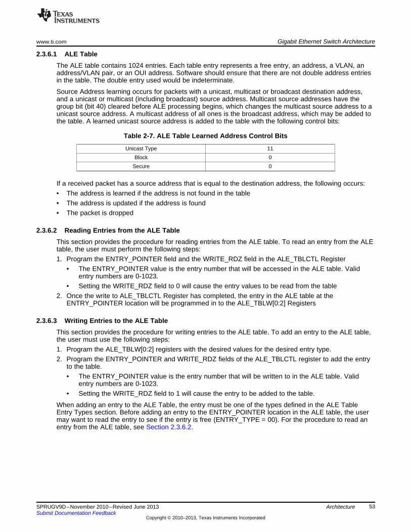
www.ti.com Gigabit Ethernet Switch Architecture
53SPRUGV9D–November 2010–Revised June 2013Submit Documentation Feedback
Copyright © 2010–2013, Texas Instruments Incorporated
Architecture
2.3.6.1 ALE TableThe ALE table contains 1024 entries. Each table entry represents a free entry, an address, a VLAN, anaddress/VLAN pair, or an OUI address. Software should ensure that there are not double address entriesin the table. The double entry used would be indeterminate.
Source Address learning occurs for packets with a unicast, multicast or broadcast destination address,and a unicast or multicast (including broadcast) source address. Multicast source addresses have thegroup bit (bit 40) cleared before ALE processing begins, which changes the multicast source address to aunicast source address. A multicast address of all ones is the broadcast address, which may be added tothe table. A learned unicast source address is added to the table with the following control bits:
Table 2-7. ALE Table Learned Address Control Bits
Unicast Type 11Block 0
Secure 0
If a received packet has a source address that is equal to the destination address, the following occurs:• The address is learned if the address is not found in the table• The address is updated if the address is found• The packet is dropped
2.3.6.2 Reading Entries from the ALE TableThis section provides the procedure for reading entries from the ALE table. To read an entry from the ALEtable, the user must perform the following steps:1. Program the ENTRY_POINTER field and the WRITE_RDZ field in the ALE_TBLCTL Register
• The ENTRY_POINTER value is the entry number that will be accessed in the ALE table. Validentry numbers are 0-1023.
• Setting the WRITE_RDZ field to 0 will cause the entry values to be read from the table2. Once the write to ALE_TBLCTL Register has completed, the entry in the ALE table at the
ENTRY_POINTER location will be programmed in to the ALE_TBLW[0:2] Registers
2.3.6.3 Writing Entries to the ALE TableThis section provides the procedure for writing entries to the ALE table. To add an entry to the ALE table,the user must use the following steps:1. Program the ALE_TBLW[0:2] registers with the desired values for the desired entry type.2. Program the ENTRY_POINTER and WRITE_RDZ fields of the ALE_TBLCTL register to add the entry
to the table.• The ENTRY_POINTER value is the entry number that will be written to in the ALE table. Valid
entry numbers are 0-1023.• Setting the WRITE_RDZ field to 1 will cause the entry to be added to the table.
When adding an entry to the ALE Table, the entry must be one of the types defined in the ALE TableEntry Types section. Before adding an entry to the ENTRY_POINTER location in the ALE table, the usermay want to read the entry to see if the entry is free (ENTRY_TYPE = 00). For the procedure to read anentry from the ALE table, see Section 2.3.6.2.
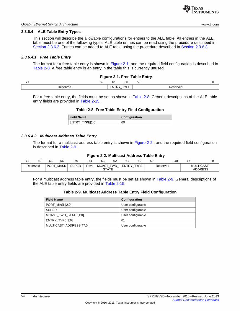
Gigabit Ethernet Switch Architecture www.ti.com
54 SPRUGV9D–November 2010–Revised June 2013Submit Documentation Feedback
Copyright © 2010–2013, Texas Instruments Incorporated
Architecture
2.3.6.4 ALE Table Entry TypesThis section will describe the allowable configurations for entries to the ALE table. All entries in the ALEtable must be one of the following types. ALE table entries can be read using the procedure described inSection 2.3.6.2. Entries can be added to ALE table using the procedure described in Section 2.3.6.3.
2.3.6.4.1 Free Table EntryThe format for a free table entry is shown in Figure 2-1, and the required field configuration is described inTable 2-8. A free table entry is an entry in the table this is currently unused.
Figure 2-1. Free Table Entry71 62 61 60 59 0
Reserved ENTRY_TYPE Reserved
For a free table entry, the fields must be set as shown in Table 2-8. General descriptions of the ALE tableentry fields are provided in Table 2-15.
Table 2-8. Free Table Entry Field Configuration
Field Name ConfigurationENTRY_TYPE[1:0] 00
2.3.6.4.2 Multicast Address Table EntryThe format for a multicast address table entry is shown in Figure 2-2 , and the required field configurationis described in Table 2-9.
Figure 2-2. Multicast Address Table Entry71 69 68 66 65 64 63 62 61 60 59 48 47 0Reserved PORT_MASK SUPER Rsvd MCAST_FWD_
STATEENTRY_TYPE Reserved MULTICAST
_ADDRESS
For a multicast address table entry, the fields must be set as shown in Table 2-9. General descriptions ofthe ALE table entry fields are provided in Table 2-15.
Table 2-9. Multicast Address Table Entry Field Configuration
Field Name ConfigurationPORT_MASK[2:0] User configurableSUPER User configurableMCAST_FWD_STATE[1:0] User configurableENTRY_TYPE[1:0] 01MULTICAST_ADDRESS[47:0] User configurable
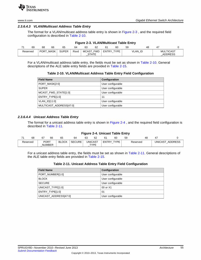
www.ti.com Gigabit Ethernet Switch Architecture
55SPRUGV9D–November 2010–Revised June 2013Submit Documentation Feedback
Copyright © 2010–2013, Texas Instruments Incorporated
Architecture
2.3.6.4.3 VLAN/Multicast Address Table EntryThe format for a VLAN/multicast address table entry is shown in Figure 2-3 , and the required fieldconfiguration is described in Table 2-10.
Figure 2-3. VLAN/Multicast Table Entry71 69 68 66 65 64 63 62 61 60 59 48 47 0Reserved PORT_MASK SUPER Rsvd MCAST_FWD
_STATEENTRY_TYPE VLAN_ID MULTICAST
_ADDRESS
For a VLAN/multicast address table entry, the fields must be set as shown in Table 2-10. Generaldescriptions of the ALE table entry fields are provided in Table 2-15.
Table 2-10. VLAN/Multicast Address Table Entry Field Configuration
Field Name ConfigurationPORT_MASK[2:0] User configurableSUPER User configurableMCAST_FWD_STATE[1:0] User configurableENTRY_TYPE[1:0] 11VLAN_ID[11:0] User configurableMULTICAST_ADDRESS[47:0] User configurable
2.3.6.4.4 Unicast Address Table EntryThe format for a unicast address table entry is shown in Figure 2-4 , and the required field configuration isdescribed in Table 2-11.
Figure 2-4. Unicast Table Entry71 68 67 66 65 64 63 62 61 60 59 48 47 0Reserved PORT
_NUMBERBLOCK SECURE UNICAST
_TYPEENTRY_TYPE Reserved UNICAST_ADDRESS
For a unicast address table entry, the fields must be set as shown in Table 2-11. General descriptions ofthe ALE table entry fields are provided in Table 2-15.
Table 2-11. Unicast Address Table Entry Field Configuration
Field Name ConfigurationPORT_NUMBER[1:0] User configurableBLOCK User configurableSECURE User configurableUNICAST_TYPE[1:0] 00 or X1ENTRY_TYPE[1:0] 01UNICAST_ADDRESS[47:0] User configurable
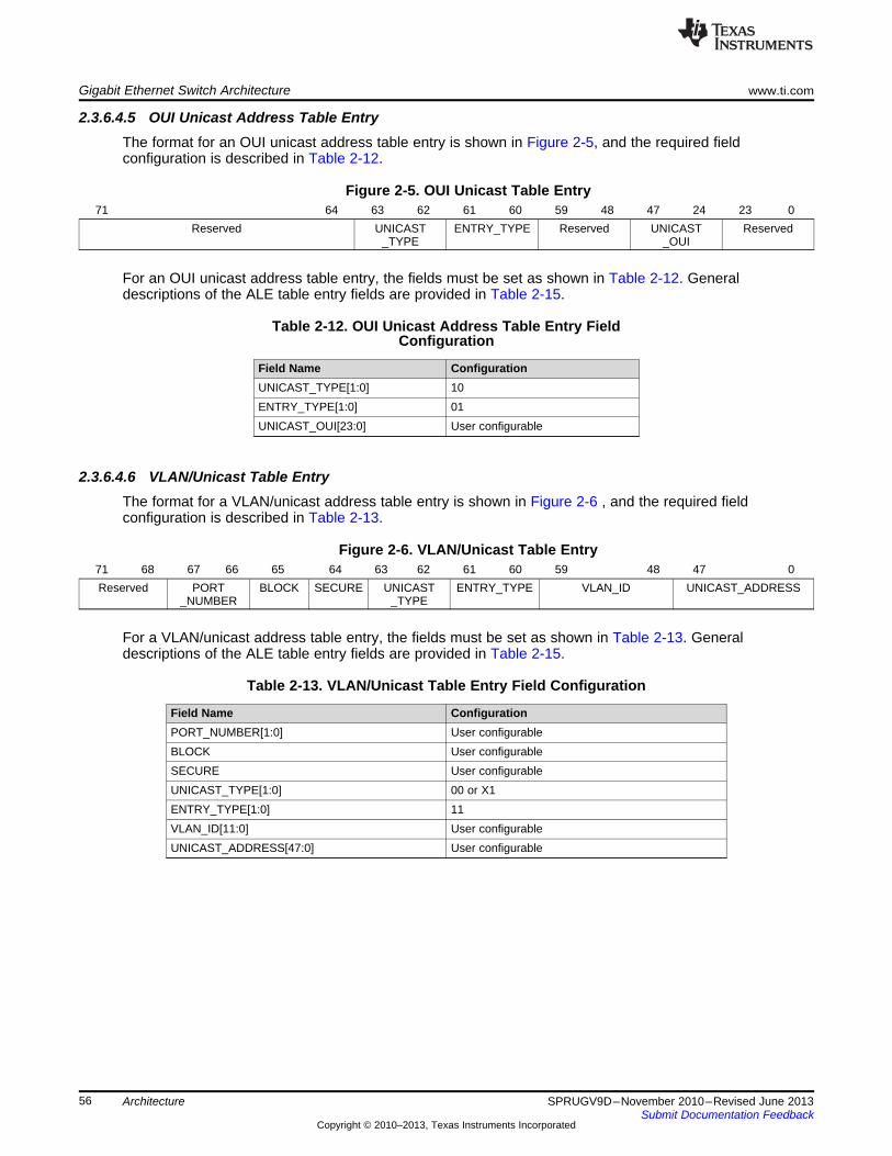
Gigabit Ethernet Switch Architecture www.ti.com
56 SPRUGV9D–November 2010–Revised June 2013Submit Documentation Feedback
Copyright © 2010–2013, Texas Instruments Incorporated
Architecture
2.3.6.4.5 OUI Unicast Address Table EntryThe format for an OUI unicast address table entry is shown in Figure 2-5, and the required fieldconfiguration is described in Table 2-12.
Figure 2-5. OUI Unicast Table Entry71 64 63 62 61 60 59 48 47 24 23 0
Reserved UNICAST_TYPE
ENTRY_TYPE Reserved UNICAST_OUI
Reserved
For an OUI unicast address table entry, the fields must be set as shown in Table 2-12. Generaldescriptions of the ALE table entry fields are provided in Table 2-15.
Table 2-12. OUI Unicast Address Table Entry FieldConfiguration
Field Name ConfigurationUNICAST_TYPE[1:0] 10ENTRY_TYPE[1:0] 01UNICAST_OUI[23:0] User configurable
2.3.6.4.6 VLAN/Unicast Table EntryThe format for a VLAN/unicast address table entry is shown in Figure 2-6 , and the required fieldconfiguration is described in Table 2-13.
Figure 2-6. VLAN/Unicast Table Entry71 68 67 66 65 64 63 62 61 60 59 48 47 0Reserved PORT
_NUMBERBLOCK SECURE UNICAST
_TYPEENTRY_TYPE VLAN_ID UNICAST_ADDRESS
For a VLAN/unicast address table entry, the fields must be set as shown in Table 2-13. Generaldescriptions of the ALE table entry fields are provided in Table 2-15.
Table 2-13. VLAN/Unicast Table Entry Field Configuration
Field Name ConfigurationPORT_NUMBER[1:0] User configurableBLOCK User configurableSECURE User configurableUNICAST_TYPE[1:0] 00 or X1ENTRY_TYPE[1:0] 11VLAN_ID[11:0] User configurableUNICAST_ADDRESS[47:0] User configurable
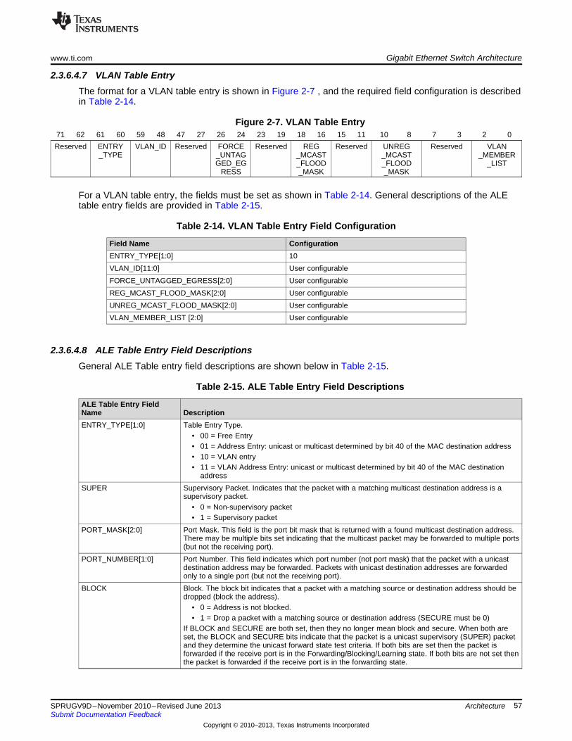
www.ti.com Gigabit Ethernet Switch Architecture
57SPRUGV9D–November 2010–Revised June 2013Submit Documentation Feedback
Copyright © 2010–2013, Texas Instruments Incorporated
Architecture
2.3.6.4.7 VLAN Table EntryThe format for a VLAN table entry is shown in Figure 2-7 , and the required field configuration is describedin Table 2-14.
Figure 2-7. VLAN Table Entry71 62 61 60 59 48 47 27 26 24 23 19 18 16 15 11 10 8 7 3 2 0Reserved ENTRY
_TYPEVLAN_ID Reserved FORCE
_UNTAGGED_EG
RESS
Reserved REG_MCAST_FLOOD_MASK
Reserved UNREG_MCAST_FLOOD_MASK
Reserved VLAN_MEMBER
_LIST
For a VLAN table entry, the fields must be set as shown in Table 2-14. General descriptions of the ALEtable entry fields are provided in Table 2-15.
Table 2-14. VLAN Table Entry Field Configuration
Field Name ConfigurationENTRY_TYPE[1:0] 10VLAN_ID[11:0] User configurableFORCE_UNTAGGED_EGRESS[2:0] User configurableREG_MCAST_FLOOD_MASK[2:0] User configurableUNREG_MCAST_FLOOD_MASK[2:0] User configurableVLAN_MEMBER_LIST [2:0] User configurable
2.3.6.4.8 ALE Table Entry Field DescriptionsGeneral ALE Table entry field descriptions are shown below in Table 2-15.
Table 2-15. ALE Table Entry Field Descriptions
ALE Table Entry FieldName DescriptionENTRY_TYPE[1:0] Table Entry Type.
• 00 = Free Entry• 01 = Address Entry: unicast or multicast determined by bit 40 of the MAC destination address• 10 = VLAN entry• 11 = VLAN Address Entry: unicast or multicast determined by bit 40 of the MAC destination
addressSUPER Supervisory Packet. Indicates that the packet with a matching multicast destination address is a
supervisory packet.• 0 = Non-supervisory packet• 1 = Supervisory packet
PORT_MASK[2:0] Port Mask. This field is the port bit mask that is returned with a found multicast destination address.There may be multiple bits set indicating that the multicast packet may be forwarded to multiple ports(but not the receiving port).
PORT_NUMBER[1:0] Port Number. This field indicates which port number (not port mask) that the packet with a unicastdestination address may be forwarded. Packets with unicast destination addresses are forwardedonly to a single port (but not the receiving port).
BLOCK Block. The block bit indicates that a packet with a matching source or destination address should bedropped (block the address).
• 0 = Address is not blocked.• 1 = Drop a packet with a matching source or destination address (SECURE must be 0)
If BLOCK and SECURE are both set, then they no longer mean block and secure. When both areset, the BLOCK and SECURE bits indicate that the packet is a unicast supervisory (SUPER) packetand they determine the unicast forward state test criteria. If both bits are set then the packet isforwarded if the receive port is in the Forwarding/Blocking/Learning state. If both bits are not set thenthe packet is forwarded if the receive port is in the forwarding state.
Gigabit Ethernet Switch Architecture www.ti.com
58 SPRUGV9D–November 2010–Revised June 2013Submit Documentation Feedback
Copyright © 2010–2013, Texas Instruments Incorporated
Architecture
Table 2-15. ALE Table Entry Field Descriptions (continued)ALE Table Entry FieldName DescriptionSECURE Secure. This bit indicates that a packet with a matching source address should be dropped if the
received port number is not equal to the table entry PORT_NUMBER.• 0 = Received port number is a don’t care• 1 = Drop the packet if the received port is not the secure port for the source address and do not
update the address (BLOCK must be 0)UNICAST_TYPE[1:0] Unicast Type. This field indicates the type of unicast address the table entry contains.
• 00 = Unicast address that is not ageable• 01 = Ageable unicast address that has not been touched• 10 = OUI address - lower 24-bits are don’t cares (not ageable)• 11 = Ageable unicast address that has been touched
MCAST_FWD_STATE[1:0] Multicast Forward State. Indicates the port state(s) required for the received port on a destinationaddress lookup in order for the multicast packet to be forwarded to the transmit port(s). A transmitport must be in the Forwarding state in order to forward the packet. If the transmit PORT_MASK hasmultiple set bits then each forward decision is independent of the other transmit port(s) forwarddecision.
• 00 = Forwarding• 01 = Blocking/Forwarding/Learning• 10 = Forwarding/Learning• 11 = Forwarding
The forward state test returns a true value if both the receive and transmit ports are in the requiredstate.
VLAN_ID VLAN_ID. This is the 12-bit VLAN ID.ADDRESS Packet Address. This is the 48-bit packet MAC address. For an OUI address, only the upper 24-bits
of the address are used in the source or destination address lookup. Otherwise, all 48-bits are usedin the lookup.
VLAN_MEMBER_LIST VLAN Member List. This six bit field indicates which port(s) are a member of the associated VLAN.UNREG_MCAST_FLOOD_MASK
Unregistered Multicast Flood Mask. Mask used for multicast when the multicast address is not found
REG_MCAST_FLOOD_MASK
Registered Multicast Flood Mask. Mask used for multicast when the multicast address is found.
FORCE_UNTAGGED_EGRESS
Force Untagged Packet Egress. Causes the packet VLAN tag to be removed on egress.
2.3.6.5 ALE Packet Forwarding ProcessThis section describes the packet forwarding process used by the ALE. For each packet sent to the ALE,it will decide whether or not the packet should be dropped or forwarded. If the packet is forwarded, thenthe ALE needs to determine which switch port or ports a packet the should be forwarded to. Each port hasan associated packet forwarding state that can be set to one of four values:• Disabled• Blocked• Learning• Forwarding
By default, all ports are disabled. To enable a port, the host must set the packet forwarding state in therespective ALE_PORTCTL register. The receive packet processes are described in the following sections.The state of each port will affect whether or not a packet is forwarded.
There are four processes that an packet may go through to determine packet forwarding. The processesare:• Ingress Filtering• VLAN Aware Lookup• VLAN Unaware Lookup• Egress
www.ti.com Gigabit Ethernet Switch Architecture
59SPRUGV9D–November 2010–Revised June 2013Submit Documentation Feedback
Copyright © 2010–2013, Texas Instruments Incorporated
Architecture
The packet forwarding process begins with the ingress filtering process. In the packet ingress process,there is one forward state test for unicast destination addresses, and another forward state test formulticast addresses. The forward state test that is used is determined by bit 40 of the destination addressin the packet, which will designate the packet as multicast or unicast.The multicast forward state testindicates the port states required for the receiving port in order for the multicast packet to be forwarded tothe transmit port(s). A transmit port must be in the Forwarding state for the packet to be forwarded fortransmission. The MCAST_FWD_STATE indicates the required port state for the receiving port asindicated in the ALE table entry field descriptions above.
The unicast forward state test indicates the port state required for the receiving port in order to forward theunicast packet. The transmit port must be in the Forwarding state in order to forward the packet. The blockand secure bits determine the unicast forward state test criteria. If both bits are set then the packet isforwarded if the receive port is in the Forwarding/Blocking/Learning state. If both bits are not set then thepacket is forwarded if the receive port is in the Forwarding state. The transmit port must be in theForwarding state regardless.
In general, packets received with errors are dropped by the address lookup engine in the ingress filteringprocess without learning, updating, or touching the addresses in the ALE table. The error condition andthe abort are indicated by the MAC module to the ALE. Packets with errors may be passed to the host(not aborted) by a MAC port if the RX_CMF_EN, RX_CEF_EN, or RX_CSF_EN bit(s) have been set in theMAC_CONTROL register in the MAC module. Error packets that are passed to the host by the MACmodule are considered to be bypass packets by the ALE and are sent only to the host. Error packets donot learn, update, or touch addresses in the ALE table regardless of whether they are aborted or sent tothe host. Packets with errors received by the host are dropped.• RX_CEF_EN – This bit in the MAC_CONTROL register enables frames that are fragments, long,
jabber, CRC, code, and alignment errors to be forwarded• RX_CSF_EN – This bit in the MAC_CONTROL register enables short frames to be forwarded• RX_CMF_EN – This bit in the MAC_CONTROL register enables MAC control frames to be forwarded.
If RX_CEF_EN, RX_CSF_EN, RX_CMF_EN bits are enabled in the configuration, then the packets thatare sent with the errors that correspond to these flags' descriptions (i.e., these bits) will be copied tomemory. Their corresponding error flag in the descriptor will be enabled. The error values are shown inTable 2-16.
Table 2-16. Gigabit Ethernet Switch Subsystem Descriptor Error Flags
ErrorThe values listed in the error flags field of the descriptor are defined as follows:
• x000 = no error• x001 = packet CRC error on ingress• x010 = packet code error on ingress• x011 = packet alignment error on ingress• x1xx = middle of packet overrun on egress• 1xxx = Indicates that the descriptor protocol specific flags section has a set long, short, or mac_ctl bit
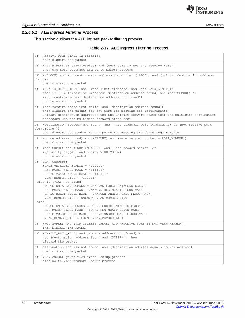
Gigabit Ethernet Switch Architecture www.ti.com
60 SPRUGV9D–November 2010–Revised June 2013Submit Documentation Feedback
Copyright © 2010–2013, Texas Instruments Incorporated
Architecture
2.3.6.5.1 ALE Ingress Filtering ProcessThis section outlines the ALE ingress packet filtering process.
Table 2-17. ALE Ingress Filtering Process
If (Receive PORT_STATE is Disabled)then discard the packet
if ((ALE_BYPASS or error packet) and (host port is not the receive port))then use host portmask and go to Egress process
if (((BLOCK) and (unicast source address found)) or ((BLOCK) and (unicast destination addressfound)))
then discard the packet
if ((ENABLE_RATE_LIMIT) and (rate limit exceeded) and (not RATE_LIMIT_TX)then if (((multicast or broadcast destination address found) and (not SUPER)) or(multicast/broadcast destination address not found))then discard the packet
if ((not forward state test valid) and (destination address found))then discard the packet for any port not meeting the requirementsUnicast destination addresses use the unicast forward state test and multicast destinationaddresses use the multicast forward state test.
if ((destination address not found) and ((not transmit port forwarding) or (not receive portforwarding)))
then discard the packet to any ports not meeting the above requirements
if (source address found) and (SECURE) and (receive port number!= PORT_NUMBER))then discard the packet
if ((not SUPER) and (DROP_UNTAGGED) and ((non-tagged packet) or((priority tagged) and not(EN_VID0_MODE))then discard the packet
If (VLAN_Unaware)FORCE_UNTAGGED_EGRESS = "000000"
REG_MCAST_FLOOD_MASK = "111111"UNREG_MCAST_FLOOD_MASK = "111111"VLAN_MEMBER_LIST = "111111"
else if (VLAN not found)FORCE_UNTAGGED_EGRESS = UNKNOWN_FORCE_UNTAGGED_EGRESSREG_MCAST_FLOOD_MASK = UNKNOWN_REG_MCAST_FLOOD_MASKUNREG_MCAST_FLOOD_MASK = UNKNOWN UNREG_MCAST_FLOOD_MASKVLAN_MEMBER_LIST = UNKNOWN_VLAN_MEMBER_LIST
elseFORCE_UNTAGGED_EGRESS = FOUND FORCE_UNTAGGED_EGRESSREG_MCAST_FLOOD_MASK = FOUND REG_MCAST_FLOOD_MASKUNREG_MCAST_FLOOD_MASK = FOUND UNREG_MCAST_FLOOD_MASKVLAN_MEMBER_LIST = FOUND VLAN_MEMBER_LIST
IF ((NOT SUPER) AND (VID_INGRESS_CHECK) AND (RECEIVE PORT IS NOT VLAN MEMBER))THEN DISCARD THE PACKET
if ((ENABLE_AUTH_MODE) and (source address not found) andnot (destination address found and (SUPER))) thendiscard the packet
if (destination address not found) and (destination address equals source address)then discard the packet
if (VLAN_AWARE) go to VLAN aware lookup processelse go to VLAN unaware lookup process
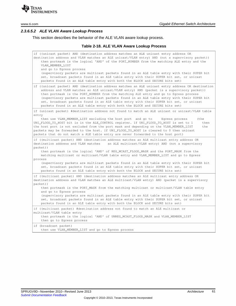
www.ti.com Gigabit Ethernet Switch Architecture
61SPRUGV9D–November 2010–Revised June 2013Submit Documentation Feedback
Copyright © 2010–2013, Texas Instruments Incorporated
Architecture
2.3.6.5.2 ALE VLAN Aware Lookup ProcessThis section describes the behavior of the ALE VLAN aware lookup process.
Table 2-18. ALE VLAN Aware Lookup Process
if ((unicast packet) AND (destination address matches an ALE unicast entry address ORdestination address and VLAN matches an ALE unicast/VLAN entry) AND (not a supervisory packet))
then portmask is the logical "AND" of the PORT_NUMBER from the matching ALE entry and theVLAN_MEMBER_LISTand go to Egress process(supervisory packets are multicast packets found in an ALE table entry with their SUPER bitset, broadcast packets found in an ALE table entry with their SUPER bit set, or unicastpackets found in an ALE table entry with both the BLOCK and SECURE bits set)
if ((unicast packet) AND (destination address matches an ALE unicast entry address OR destinationaddress and VLAN matches an ALE unicast/VLAN entry) AND (packet is a supervisory packet))then portmask is the PORT_NUMBER from the matching ALE entry and go to Egress process(supervisory packets are multicast packets found in an ALE table entry with their SUPER bitset, broadcast packets found in an ALE table entry with their SUPER bit set, or unicastpackets found in an ALE table entry with both the BLOCK and SECURE bits set)
if (unicast packet) #destination address not found to match an ALE unicast or unicast/VLAN tableentry
then use VLAN_MEMBER_LIST excluding the host port and go to Egress process (theUNI_FLOOD_TO_HOST bit is in the ALE_CONTROL register. If UNI_FLOOD_TO_HOST is set to 1 thenthe host port is not excluded from the port mask and depending on the VLAN_MEMBER_LIST thepackets may be forwarded to the host. If UNI_FLOOD_TO_HOST is cleared to 0 then unicastpackets that do not match a ALE table entry are never forwarded to the host port)
if ((multicast packet) AND (destination address matches an ALE multicast entry address ORdestination address and VLAN matches an ALE multicast/VLAN entry) AND (not a supervisorypacket))
then portmask is the logical "AND" of REG_MCAST_FLOOD_MASK and the PORT_MASK from thematching multicast or multicast/VLAN table entry and VLAN_MEMBER_LIST and go to Egress
process(supervisory packets are multicast packets found in an ALE table entry with their SUPER bitset, broadcast packets found in an ALE table entry with their SUPER bit set, or unicastpackets found in an ALE table entry with both the BLOCK and SECURE bits set)
if ((multicast packet) AND (destination address matches an ALE multicast entry address ORdestination address and VLAN matches an ALE multicast/VLAN entry) AND (packet is a supervisorypacket))
then portmask is the PORT_MASK from the matching multicast or multicast/VLAN table entryand go to Egress process(supervisory packets are multicast packets found in an ALE table entry with their SUPER bitset, broadcast packets found in an ALE table entry with their SUPER bit set, or unicastpackets found in an ALE table entry with both the BLOCK and SECURE bits set)
if ((multicast packet) #destination address not found to match an ALE multicast ormulticast/VLAN table entry
then portmask is the logical "AND" of UNREG_MCAST_FLOOD_MASK and VLAN_MEMBER_LISTthen go to Egress process
if (broadcast packet)then use VLAN_MEMBER_LIST and go to Egress process
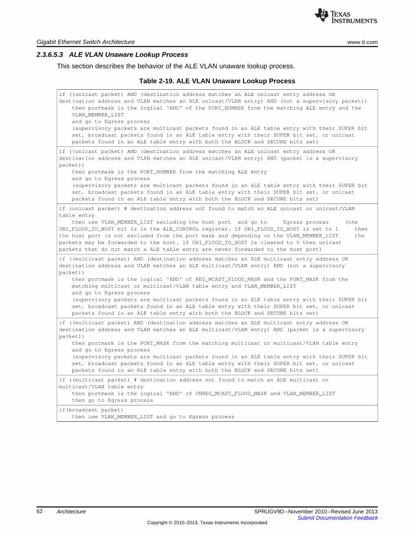
Gigabit Ethernet Switch Architecture www.ti.com
62 SPRUGV9D–November 2010–Revised June 2013Submit Documentation Feedback
Copyright © 2010–2013, Texas Instruments Incorporated
Architecture
2.3.6.5.3 ALE VLAN Unaware Lookup ProcessThis section describes the behavior of the ALE VLAN unaware lookup process.
Table 2-19. ALE VLAN Unaware Lookup Process
if ((unicast packet) AND (destination address matches an ALE unicast entry address ORdestination address and VLAN matches an ALE unicast/VLAN entry) AND (not a supervisory packet))
then portmask is the logical "AND" of the PORT_NUMBER from the matching ALE entry and theVLAN_MEMBER_LISTand go to Egress process(supervisory packets are multicast packets found in an ALE table entry with their SUPER bitset, broadcast packets found in an ALE table entry with their SUPER bit set, or unicastpackets found in an ALE table entry with both the BLOCK and SECURE bits set)
if ((unicast packet) AND (destination address matches an ALE unicast entry address ORdestination address and VLAN matches an ALE unicast/VLAN entry) AND (packet is a supervisorypacket))
then portmask is the PORT_NUMBER from the matching ALE entryand go to Egress process(supervisory packets are multicast packets found in an ALE table entry with their SUPER bitset, broadcast packets found in an ALE table entry with their SUPER bit set, or unicastpackets found in an ALE table entry with both the BLOCK and SECURE bits set)
if (unicast packet) # destination address not found to match an ALE unicast or unicast/VLANtable entry
then use VLAN_MEMBER_LIST excluding the host port and go to Egress process (theUNI_FLOOD_TO_HOST bit is in the ALE_CONTROL register. If UNI_FLOOD_TO_HOST is set to 1 thenthe host port is not excluded from the port mask and depending on the VLAN_MEMBER_LIST thepackets may be forwarded to the host. If UNI_FLOOD_TO_HOST is cleared to 0 then unicastpackets that do not match a ALE table entry are never forwarded to the host port)
if ((multicast packet) AND (destination address matches an ALE multicast entry address ORdestination address and VLAN matches an ALE multicast/VLAN entry) AND (not a supervisorypacket))
then portmask is the logical "AND" of REG_MCAST_FLOOD_MASK and the PORT_MASK from thematching multicast or multicast/VLAN table entry and VLAN_MEMBER_LISTand go to Egress process(supervisory packets are multicast packets found in an ALE table entry with their SUPER bitset, broadcast packets found in an ALE table entry with their SUPER bit set, or unicastpackets found in an ALE table entry with both the BLOCK and SECURE bits set)
if ((multicast packet) AND (destination address matches an ALE multicast entry address ORdestination address and VLAN matches an ALE multicast/VLAN entry) AND (packet is a supervisorypacket))
then portmask is the PORT_MASK from the matching multicast or multicast/VLAN table entryand go to Egress process(supervisory packets are multicast packets found in an ALE table entry with their SUPER bitset, broadcast packets found in an ALE table entry with their SUPER bit set, or unicastpackets found in an ALE table entry with both the BLOCK and SECURE bits set)
if ((multicast packet) # destination address not found to match an ALE multicast ormulticast/VLAN table entry
then portmask is the logical "AND" of UNREG_MCAST_FLOOD_MASK and VLAN_MEMBER_LISTthen go to Egress process
if(broadcast packet)then use VLAN_MEMBER_LIST and go to Egress process
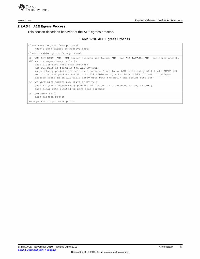
www.ti.com Gigabit Ethernet Switch Architecture
63SPRUGV9D–November 2010–Revised June 2013Submit Documentation Feedback
Copyright © 2010–2013, Texas Instruments Incorporated
Architecture
2.3.6.5.4 ALE Egress ProcessThis section describes behavior of the ALE egress process.
Table 2-20. ALE Egress Process
Clear receive port from portmask(don’t send packet to receive port)
Clear disabled ports from portmask
if ((EN_OUI_DENY) AND (OUI source address not found) AND (not ALE_BYPASS) AND (not error packet)AND (not a supervisory packet))
then clear host port from portmask(EN_OUI_DENY is found in the ALE_CONTROL)(supervisory packets are multicast packets found in an ALE table entry with their SUPER bitset, broadcast packets found in an ALE table entry with their SUPER bit set, or unicastpackets found in an ALE table entry with both the BLOCK and SECURE bits set)
if ((ENABLE_RATE_LIMIT) AND (RATE_LIMIT_TX))then if (not a supervisory packet) AND (rate limit exceeded on any tx port)then clear rate limited tx port from portmask
if (portmask is 0)then discard packet
Send packet to portmask ports
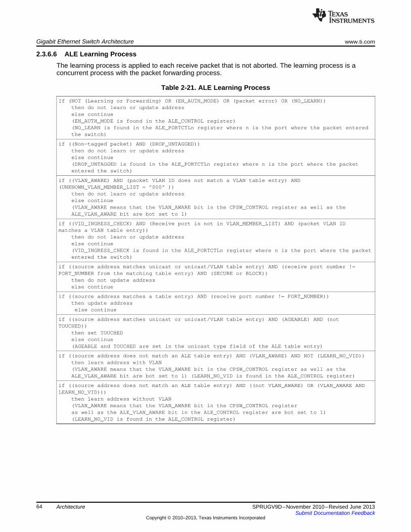
Gigabit Ethernet Switch Architecture www.ti.com
64 SPRUGV9D–November 2010–Revised June 2013Submit Documentation Feedback
Copyright © 2010–2013, Texas Instruments Incorporated
Architecture
2.3.6.6 ALE Learning ProcessThe learning process is applied to each receive packet that is not aborted. The learning process is aconcurrent process with the packet forwarding process.
Table 2-21. ALE Learning Process
If (NOT (Learning or Forwarding) OR (EN_AUTH_MODE) OR (packet error) OR (NO_LEARN))then do not learn or update addresselse continue(EN_AUTH_MODE is found in the ALE_CONTROL register)(NO_LEARN is found in the ALE_PORTCTLn register where n is the port where the packet enteredthe switch)
if ((Non-tagged packet) AND (DROP_UNTAGGED))then do not learn or update addresselse continue(DROP_UNTAGGED is found in the ALE_PORTCTLn register where n is the port where the packetentered the switch)
if ((VLAN_AWARE) AND (packet VLAN ID does not match a VLAN table entry) AND(UNKNOWN_VLAN_MEMBER_LIST = "000" ))
then do not learn or update addresselse continue(VLAN_AWARE means that the VLAN_AWARE bit in the CPSW_CONTROL register as well as theALE_VLAN_AWARE bit are bot set to 1)
if ((VID_INGRESS_CHECK) AND (Receive port is not in VLAN_MEMBER_LIST) AND (packet VLAN IDmatches a VLAN table entry))
then do not learn or update addresselse continue(VID_INGRESS_CHECK is found in the ALE_PORTCTLn register where n is the port where the packetentered the switch)
if ((source address matches unicast or unicast/VLAN table entry) AND (receive port number !=PORT_NUMBER from the matching table entry) AND (SECURE or BLOCK))
then do not update addresselse continue
if ((source address matches a table entry) AND (receive port number != PORT_NUMBER))then update address
else continue
if ((source address matches unicast or unicast/VLAN table entry) AND (AGEABLE) AND (notTOUCHED))
then set TOUCHEDelse continue(AGEABLE and TOUCHED are set in the unicast type field of the ALE table entry)
if ((source address does not match an ALE table entry) AND (VLAN_AWARE) AND NOT (LEARN_NO_VID))then learn address with VLAN(VLAN_AWARE means that the VLAN_AWARE bit in the CPSW_CONTROL register as well as theALE_VLAN_AWARE bit are bot set to 1) (LEARN_NO_VID is found in the ALE_CONTROL register)
if ((source address does not match an ALE table entry) AND ((not VLAN_AWARE) OR (VLAN_AWARE ANDLEARN_NO_VID)))
then learn address without VLAN(VLAN_AWARE means that the VLAN_AWARE bit in the CPSW_CONTROL registeras well as the ALE_VLAN_AWARE bit in the ALE_CONTROL register are bot set to 1)(LEARN_NO_VID is found in the ALE_CONTROL register)
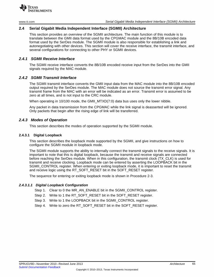
www.ti.com Serial Gigabit Media Independent Interface (SGMII) Architecture
65SPRUGV9D–November 2010–Revised June 2013Submit Documentation Feedback
Copyright © 2010–2013, Texas Instruments Incorporated
Architecture
2.4 Serial Gigabit Media Independent Interface (SGMII) ArchitectureThis section provides an overview of the SGMII architecture. The main function of this module is totranslate between the GMII data format used by the CPGMAC module and the 8B/10B encoded dataformat used by the SerDes module. The SGMII module is also responsible for establishing a link andautonegotiating with other devices. This section will cover the receive interface, the transmit interface, andseveral configurations for connecting to other PHY or SGMII devices.
2.4.1 SGMII Receive InterfaceThe SGMII receive interface converts the 8B/10B encoded receive input from the SerDes into the GMIIsignals required by the MAC module.
2.4.2 SGMII Transmit InterfaceThe SGMII transmit interface converts the GMII input data from the MAC module into the 8B/10B encodedoutput required by the SerDes module. The MAC module does not source the transmit error signal. Anytransmit frame from the MAC with an error will be indicated as an error. Transmit error is assumed to bezero at all times, and is not input to the CRC module.
When operating in 10/100 mode, the GMII_MTXD(7:0) data bus uses only the lower nibble.
Any packet in data transmission from the CPGMAC while the link signal is deasserted will be ignored.Only packets that begin after the rising edge of link will be transferred.
2.4.3 Modes of OperationThis section describes the modes of operation supported by the SGMII module.
2.4.3.1 Digital LoopbackThis section describes the loopback mode supported by the SGMII, and give instructions on how toconfigure the SGMII module in loopback mode.
The SGMII module supports the ability to internally connect the transmit signals to the receive signals. It isimportant to note that this is digital loopback, because the transmit and receive signals are connectedbefore reaching the SerDes module. When in this configuration, the transmit clock (TX_CLK) is used fortransmit and receive clocking. Loopback mode can be entered by asserting the LOOPBACK bit in theSGMII_CONTROL register. When entering or exiting loopback mode, it is important to reset the transmitand receive logic using the RT_SOFT_RESET bit in the SOFT_RESET register.
The sequence for entering or exiting loopback mode is shown in Procedure 2-3.
2.4.3.1.1 Digital Loopback ConfigurationStep 1. Clear to 0 the MR_AN_ENABLE bit in the SGMII_CONTROL register.Step 2. Write to 1 the RT_SOFT_RESET bit in the SOFT_RESET register.Step 3. Write to 1 the LOOPBACK bit in the SGMII_CONTROL register.Step 4. Write to zero the RT_SOFT_RESET bit in the SOFT_RESET register.
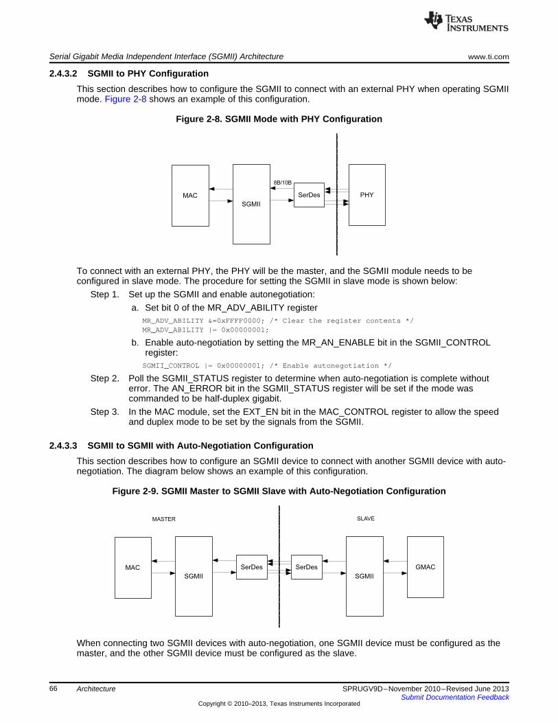
MAC
SGMII
SerDes SerDes
SGMII
GMAC
MASTER SLAVE
MAC
SGMII
SerDes PHY
8B/10B
Serial Gigabit Media Independent Interface (SGMII) Architecture www.ti.com
66 SPRUGV9D–November 2010–Revised June 2013Submit Documentation Feedback
Copyright © 2010–2013, Texas Instruments Incorporated
Architecture
2.4.3.2 SGMII to PHY ConfigurationThis section describes how to configure the SGMII to connect with an external PHY when operating SGMIImode. Figure 2-8 shows an example of this configuration.
Figure 2-8. SGMII Mode with PHY Configuration
To connect with an external PHY, the PHY will be the master, and the SGMII module needs to beconfigured in slave mode. The procedure for setting the SGMII in slave mode is shown below:
Step 1. Set up the SGMII and enable autonegotiation:a. Set bit 0 of the MR_ADV_ABILITY register
MR_ADV_ABILITY &=0xFFFF0000; /* Clear the register contents */MR_ADV_ABILITY |= 0x00000001;
b. Enable auto-negotiation by setting the MR_AN_ENABLE bit in the SGMII_CONTROLregister:
SGMII_CONTROL |= 0x00000001; /* Enable autonegotiation */
Step 2. Poll the SGMII_STATUS register to determine when auto-negotiation is complete withouterror. The AN_ERROR bit in the SGMII_STATUS register will be set if the mode wascommanded to be half-duplex gigabit.
Step 3. In the MAC module, set the EXT_EN bit in the MAC_CONTROL register to allow the speedand duplex mode to be set by the signals from the SGMII.
2.4.3.3 SGMII to SGMII with Auto-Negotiation ConfigurationThis section describes how to configure an SGMII device to connect with another SGMII device with auto-negotiation. The diagram below shows an example of this configuration.
Figure 2-9. SGMII Master to SGMII Slave with Auto-Negotiation Configuration
When connecting two SGMII devices with auto-negotiation, one SGMII device must be configured as themaster, and the other SGMII device must be configured as the slave.
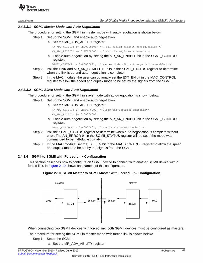
MAC
SGMII
SerDes SerDes
SGMII
MAC
MASTER MASTER
www.ti.com Serial Gigabit Media Independent Interface (SGMII) Architecture
67SPRUGV9D–November 2010–Revised June 2013Submit Documentation Feedback
Copyright © 2010–2013, Texas Instruments Incorporated
Architecture
2.4.3.3.1 SGMII Master Mode with Auto-NegotiationThe procedure for setting the SGMII in master mode with auto-negotiation is shown below:
Step 1. Set up the SGMII and enable auto-negotiation:a. Set the MR_ADV_ABILITY register
MR_ADV_ABILITY |= 0x00009801; /* Full duplex gigabit configuration */
MR_ADV_ABILITY &= 0xFFFF0000; /*Clear the register contents */
b. Enable auto-negotiation by setting the MR_AN_ENABLE bit in the SGMII_CONTROLregister:
SGMII_CONTROL |= 0x00000021; /* Master Mode with autonegotiation enabled */
Step 2. Poll the LINK and MR_AN_COMPLETE bits in the SGMII_STATUS register to determinewhen the link is up and auto-negotiation is complete.
Step 3. In the MAC module, the user can optionally set the EXT_EN bit in the MAC_CONTROLregister to allow the speed and duplex mode to be set by the signals from the SGMII.
2.4.3.3.2 SGMII Slave Mode with Auto-NegotiationThe procedure for setting the SGMII in slave mode with auto-negotiation is shown below:
Step 1. Set up the SGMII and enable auto-negotiation:a. Set the MR_ADV_ABILITY register
MR_ADV_ABILITY &= 0xFFFF0000; /*Clear the register contents*/
MR_ADV_ABILITY |= 0x00000001;
b. Enable auto-negotiation by setting the MR_AN_ENABLE bit in the SGMII_CONTROLregister:
SGMII_CONTROL |= 0x00000001; /* Enable auto-negotiation */
Step 2. Poll the SGMII_STATUS register to determine when auto-negotiation is complete withouterror. The AN_ERROR bit in the SGMII_STATUS register will be set if the mode wascommanded to be half-duplex gigabit.
Step 3. In the MAC module, set the EXT_EN bit in the MAC_CONTROL register to allow the speedand duplex mode to be set by the signals from the SGMII.
2.4.3.4 SGMII to SGMII with Forced Link ConfigurationThis section describes how to configure an SGMII device to connect with another SGMII device with aforced link. in Figure 2-10 shows an example of this configuration.
Figure 2-10. SGMII Master to SGMII Master with Forced Link Configuration
When connecting two SGMII devices with forced link, both SGMII devices must be configured as masters.
The procedure for setting the SGMII in master mode with forced link is shown below:Step 1. Setup the SGMII:
a. Set the MR_ADV_ABILITY register
Management Data Input/Output (MDIO) Architecture www.ti.com
68 SPRUGV9D–November 2010–Revised June 2013Submit Documentation Feedback
Copyright © 2010–2013, Texas Instruments Incorporated
Architecture
MR_ADV_ABILITY &= 0xFFFF0000; /* Clear the register contents */
MR_ADV_ABILITY |= 0x00009801; /* Full duplex gigabit configuration */
b. Set the device in master mode without auto-negotiation by setting the MASTER bit in theSGMII_CONTROL register:
SGMII_CONTROL |= 0x00000020; /* Master Mode, no auto-negotiation */
Step 2. Poll the LINK bit in the SGMII_STATUS register to determine when the link is up.Step 3. In the MAC module, the user must set the EXT_EN bit in the MAC_CONTROL register to
allow the speed and duplex mode to be set by the signals from the SGMII.
2.5 Management Data Input/Output (MDIO) ArchitectureThis section describes the architecture of the Management Data Input/Output (MDIO) module. The MDIOmodule manages up to 32 physical layer (PHY) devices connected to the Ethernet Media AccessController (EMAC). The MDIO module allows almost transparent operation of the MDIO interface with littlemaintenance from the DSP.
The MDIO module enumerates all PHY devices in the system by continuously polling 32 MDIO addresses.Once it detects a PHY device, the MDIO module reads the PHY status register to monitor the PHY linkstate. The MDIO module stores link change events that can interrupt the CPU. The event storage allowsthe DSP to poll the link status of the PHY device without continuously performing MDIO module accesses.When the system must access the MDIO module for configuration and negotiation, the MDIO moduleperforms the MDIO read or write operation independent of the DSP. This independent operation allowsthe DSP to poll for completion or interrupt the CPU once the operation has completed.
2.5.1 Global PHY Detection and Link State MonitoringThe MDIO module enumerates all PHY devices in the system by continuously polling the link status fromthe Generic Status Register of all 32 MDIO addresses. The module tracks whether a PHY on a particularaddress has responded, storing the results in the MDIO_ALIVE Register. The MDIO module also trackswhether the PHY currently has a link, storing the results in the MDIO_LINK Register. This informationallows the software application to quickly determine which MDIO address the PHY is using and if thesystem is using more than one PHY. The software application can then quickly switch between PHYsbased on their current link status. The link status of two of the 32 possible PHY addresses can also bedetermined using the MLINK pin inputs. The LINKSEL bit in the MDIO_USERPHYSEL n Registerdetermines the status input that is used. A change in the link status of the two PHYs being monitored willset the appropriate bit in the MDIO_LINKINTRAW Register and the MDIO_LINKINTMASKED Register, ifenabled by the LINKINTENB bit in the MDIO_USERPHYSEL n Register.
2.5.2 PHY Register User AccessWhen the DSP must access the MDIO for configuration and negotiation, the PHY access module performsthe actual MDIO read or write operation independent of the DSP. Thus, the DSP can poll for completion orreceive an interrupt when the read or write operation has been performed. There are two user accessregisters, MDIO_USERACCESS0 and MDIO_USERACCESS1, which allow the software to submit up totwo access requests simultaneously. The requests are processed sequentially.
At any time, the host can define a transaction for the MDIO module to undertake using the DATA,PHYADR , REGADR, and WRITE fields in the MDIO_USERACCESS n register . When the host sets theGO bit in this register, the MDIO module will begin the transaction without any further intervention from thehost. Upon completion, the MDIO interface will clear the GO bit and set the MDIO_USERINTRAW bit inthe MDIO_USERINTRAW register corresponding to the MDIO_USERACCESS n register being used. Thecorresponding bit in the MDIO_USERINTMASKED register may also be set depending on the masksetting in the MDIO_USERINTMASKSET and MDIO_USERINTMASKCLR registers. A round-robinarbitration scheme is used to schedule transactions that may be queued by the host in differentMDIO_USERACCESS n registers. The host should check the status of the GO bit in theMDIO_USERACCESS n register before initiating a new transaction to ensure that the previous transactionhas completed. The host can use the ACK bit in the MDIO_USERACCESS n register to determine thestatus of a read transaction. In addition, any PHY register read transactions initiated by the host alsocause the MDIO_ALIVE register to be updated.
www.ti.com Management Data Input/Output (MDIO) Architecture
69SPRUGV9D–November 2010–Revised June 2013Submit Documentation Feedback
Copyright © 2010–2013, Texas Instruments Incorporated
Architecture
2.5.2.1 Writing Data to a PHY RegisterThe MDIO module includes a user access register (MDIO_USERACCESS n) to directly access a specifiedPHY device. To write a PHY register, perform the following steps:1. Ensure that the GO bit in the MDIO_USERACCESS n register is cleared.2. Write to the GO, WRITE, REGADR , PHYADR, and DATA bits in MDIO_USERACCESS n
corresponding to the desired PHY and PHY register.3. The write operation to the PHY is scheduled and completed by the MDIO module.4. Completion of the write operation will clear the GO bit to 0, and sets the corresponding bit in the
MDIO_USERINTRAW register for the corresponding MDIO_USERACCESS n.• If interrupts have been enabled on this bit using the MDIO_USERINTMASKSET register, then the
bit is also set in the MDIO_USERINTMASKED register and an interrupt is triggered on the DSP.• If interrupts have not been enabled, then completion can be determined by polling the GO bit in
MDIO_USERACCESS n for a 0.• polling the GO bit in USERACCESSn for a 0.
Management Data Input/Output (MDIO) Architecture www.ti.com
70 SPRUGV9D–November 2010–Revised June 2013Submit Documentation Feedback
Copyright © 2010–2013, Texas Instruments Incorporated
Architecture
2.5.2.2 Reading Data from a PHY RegisterThe MDIO module includes a user access register (MDIO_USERACCESS n) to directly access a specifiedPHY device. To read a PHY register, perform the following:1. Ensure that the GO bit in the MDIO_USERACCESS n register is cleared.2. Write to the GO, REGADR , and PHYADR bits in USERACCESS n corresponding to the desired PHY
and PHY register .3. The read data value is available in the DATA bits of MDIO_USERACCESS n after the module
completes the read operation on the serial bus.4. Completion of a successful read operation will clear the GO bit, set the ACK bit, and set the
corresponding bit in the MDIO_USERINTRAW register for the MDIO_USERACCESS n used.• If interrupts have been enabled on this bit using the MDIO_USERINTMASKSET register, then the
bit is also set in the MDIO_USERINTMASKED register and an interrupt is triggered on the DSP.• If interrupts have not been enabled, then completion can be determined by polling the GO bit in
MDIO_USERACCESS n for a 0, and the ACK bit for a 1.
2.5.3 MDIO InterruptsThe MDIO module provides two sets of interrupts that can be enabled by the user. The first set ofinterrupts is triggered when there is a change in link state of a PHY that is being monitored. The secondset of interrupts will occur when a PHY register access initiated through the MDIO_USERACCESSregisters has completed.
2.5.3.1 MDIO User Access InterruptsWhen the GO bit in the MDIO_USERACCESS registers transitions from 1 to 0, indicating the completionof a user access, and the corresponding MDIO_USERINTMASKED bit in the MDIO_USERINTMASKSETregister is set, the MDIO_USERINTMASKED signal is asserted to 1.
The MDIO_USERINTMASKED event is also captured in the MDIO_USERINTMASKED register.MDIO_USERINTMASKED[0] and MDIO_USERINTMASKED[1] correspond to the MDIO_USERACCESS0and MDIO_USERACCESS1 registers, respectively.
2.5.4 Initializing the MDIO ModuleTo have the application software or device driver initialize the MDIO device, perform the following steps:1. Configure the PREAMBLE and CLKDIV bits in the MDIO_CONTROL register.2. Enable the MDIO module by setting the ENABLE bit in the MDIO_CONTROL register.3. The MDIO_ALIVE register can be read after a delay to determine which PHYs responded, and the
MDIO_LINK register can determine which of those (if any) already have a link.4. Set up the appropriate PHY addresses in the MDIO_USERPHYSEL n register, and set the
LINKINTENB bit to enable a link change event interrupt if desirable.5. If an interrupt on a general MDIO register access is desired, set the corresponding bit in the
MDIO_USERINTMASKSET register to use the MDIO_USERACCESS n register. If only one PHY is tobe used, the application software can set up one of the MDIO_USERACCESS n registers to trigger acompletion interrupt. The other register is not set up.
www.ti.com KeyStone I Serializer/Deserializer (SerDes) Architecture
71SPRUGV9D–November 2010–Revised June 2013Submit Documentation Feedback
Copyright © 2010–2013, Texas Instruments Incorporated
Architecture
2.6 KeyStone I Serializer/Deserializer (SerDes) ArchitectureThe SerDes macro is a self-contained macro that includes two transmitter (TX) and receiver (RX) pairs,and phase-locked-loop (PLL). Each transmitter and receiver pair interfaces to one of the SGMII modules.The internal PLL multiplies a user-supplied reference clock.
NOTE: The SGMII_SERDES registers are located in the chip configuration section of the device.Before writing to these registers, the kicker mechanism must be used to unlock theseregisters. For more information about using the kicker mechanism, see the device specificdata manual.
2.7 KeyStone II Serializer/Deserializer (SerDes) ArchitectureSerDes module information for KeyStone II devices is not provided in this user's guide. Check foravailability of the SerDes User's Guide for KeyStone II Devices on the device product page.
2.8 Reset ConsiderationsThe GbE switch subsystem supports reset isolation of the two Ethernet switch ports in KeyStone I, or fourin KeyStone II. The intent of reset isolation is to allow packets to switch between the two Ethernet portswhile the remainder of the system is undergoing a reset. When the ISOLATE input is asserted the belowoccur simultaneously:• The GbE switch host port (port 0) is removed from ALE processing (packets received on ports 1 and 2
intended for port 0 will be dropped)• Packets from the queue manager subsystem intended the GbE switch host port (port 0) are dropped.
Any packet currently in progress when ISOLATE is asserted is dropped due to a receive packet codeerror (and possible a CRC or FRAG error)
• GbE switch host port (port 0) egress packets in queue are dropped• (For KeyStone II) The asynchronous FIFOs on the streaming packet interface are reset.
For more information about reset isolation for the GbE switch subsystem, see the device-specific datamanual.
2.9 InitializationThis section describes the GbE switch subsystem initialization procedure.
2.9.1 GbE Switch Subsystem Initialization ProcedureStep 1. Configure the CPSW_CONTROL registerStep 2. Configure the MAC1_SA and MAC2_SA (MAC3_SA and MAC4_SA if KeyStone II) source
address hi and lo registersStep 3. Enable the desired statistics ports by programming the CPSW_STAT_PORT_EN registerStep 4. Configure the ALEStep 5. Configure MAC modulesStep 6. Configure the MDIO and external PHY (if used)Step 7. Configure the SGMII modules
Interrupt Support www.ti.com
72 SPRUGV9D–November 2010–Revised June 2013Submit Documentation Feedback
Copyright © 2010–2013, Texas Instruments Incorporated
Architecture
2.10 Interrupt Support
2.10.1 Interrupt EventsThis section describes the interrupts generated in the GbE switch subsystem. Within the GbE switchsubsystem, there are three modules that can generate interrupts: the MDIO module, the statistics module,and the time synchronization module. For more information about the interrupts generated by the MDIOmodule, see Section 2.5. For more information about the interrupts generated by the statistics modules,see Section 2.3.4. For more information about the interrupts generated by the time synchronizationmodule, see Section 2.3.5.
2.11 Power ManagementThe gigabit Ethernet (GbE) switch subsystem provides power management in the form of clock gating.Although the NETCP does have a power domain that can be enabled or disabled, the GbE switchsubsystem is only one of the modules in that power domain, and the power cannot be enabled or disabledfor the individual modules in the NETCP. For more information, see the device specific data manual.
73SPRUGV9D–November 2010–Revised June 2013Submit Documentation Feedback
Copyright © 2010–2013, Texas Instruments Incorporated
Registers
Chapter 3SPRUGV9D–November 2010–Revised June 2013
Registers
This chapter describes the registers available in the Ethernet switch subsystem, its submodules, and therelated registers in the SerDes module. For clarity, the registers for each module and submodule aredescribed separately. Provided for each register is a bit field description and a memory offset address.The offset address values provided are relative to the associated base address of the module. See thedevice-specific data manual for the memory address of these registers.
Topic ........................................................................................................................... Page
3.1 Summary of Modules.......................................................................................... 743.2 Gigabit Ethernet (GbE) Switch Subsystem Module ................................................. 883.3 Serial Gigabit Media Independent Interface (SGMII) module .................................... 903.4 Management Data Input/Output (MDIO) module ..................................................... 973.5 Ethernet Switch Module .................................................................................... 1123.6 Serializer/Deserializer (SerDes) SGMII Boot Configuration Registers ...................... 250
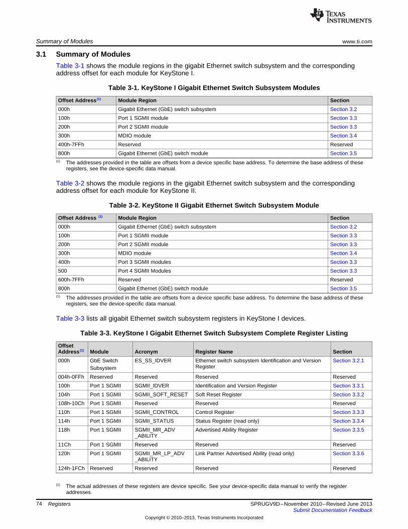
Summary of Modules www.ti.com
74 SPRUGV9D–November 2010–Revised June 2013Submit Documentation Feedback
Copyright © 2010–2013, Texas Instruments Incorporated
Registers
3.1 Summary of ModulesTable 3-1 shows the module regions in the gigabit Ethernet switch subsystem and the correspondingaddress offset for each module for KeyStone I.
(1) The addresses provided in the table are offsets from a device specific base address. To determine the base address of theseregisters, see the device-specific data manual.
Table 3-1. KeyStone I Gigabit Ethernet Switch Subsystem Modules
Offset Address (1) Module Region Section000h Gigabit Ethernet (GbE) switch subsystem Section 3.2100h Port 1 SGMII module Section 3.3200h Port 2 SGMII module Section 3.3300h MDIO module Section 3.4400h-7FFh Reserved Reserved800h Gigabit Ethernet (GbE) switch module Section 3.5
Table 3-2 shows the module regions in the gigabit Ethernet switch subsystem and the correspondingaddress offset for each module for KeyStone II.
(1) The addresses provided in the table are offsets from a device specific base address. To determine the base address of theseregisters, see the device-specific data manual.
Table 3-2. KeyStone II Gigabit Ethernet Switch Subsystem Module
Offset Address (1) Module Region Section000h Gigabit Ethernet (GbE) switch subsystem Section 3.2100h Port 1 SGMII module Section 3.3200h Port 2 SGMII module Section 3.3300h MDIO module Section 3.4400h Port 3 SGMII modules Section 3.3500 Port 4 SGMII Modules Section 3.3600h-7FFh Reserved Reserved800h Gigabit Ethernet (GbE) switch module Section 3.5
Table 3-3 lists all gigabit Ethernet switch subsystem registers in KeyStone I devices.
(1) The actual addresses of these registers are device specific. See your device-specific data manual to verify the registeraddresses.
Table 3-3. KeyStone I Gigabit Ethernet Switch Subsystem Complete Register Listing
OffsetAddress (1) Module Acronym Register Name Section000h GbE Switch
SubsystemES_SS_IDVER Ethernet switch subsystem Identification and Version
RegisterSection 3.2.1
004h-0FFh Reserved Reserved Reserved Reserved100h Port 1 SGMII SGMII_IDVER Identification and Version Register Section 3.3.1104h Port 1 SGMII SGMII_SOFT_RESET Soft Reset Register Section 3.3.2108h-10Ch Port 1 SGMII Reserved Reserved Reserved110h Port 1 SGMII SGMII_CONTROL Control Register Section 3.3.3114h Port 1 SGMII SGMII_STATUS Status Register (read only) Section 3.3.4118h Port 1 SGMII SGMII_MR_ADV
_ABILITYAdvertised Ability Register Section 3.3.5
11Ch Port 1 SGMII Reserved Reserved Reserved120h Port 1 SGMII SGMII_MR_LP_ADV
_ABILITYLink Partner Advertised Ability (read only) Section 3.3.6
124h-1FCh Reserved Reserved Reserved Reserved
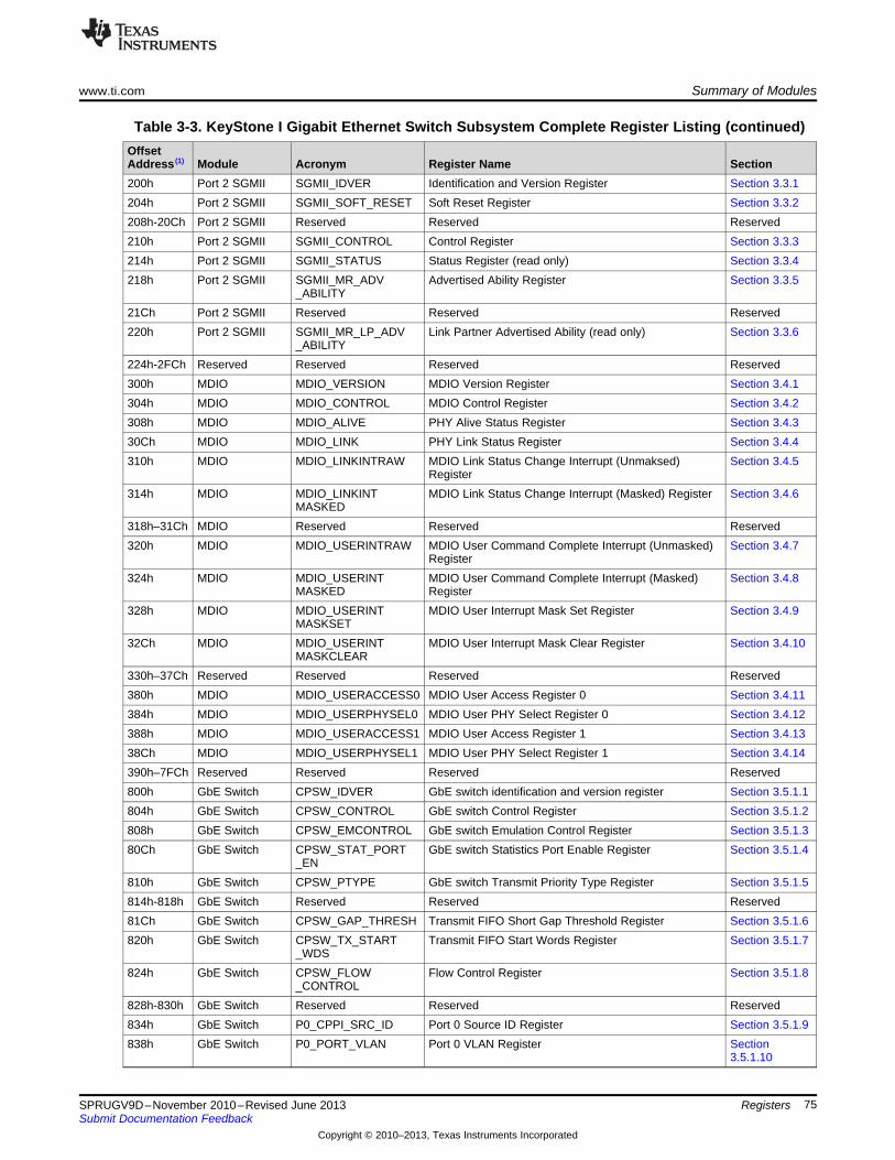
www.ti.com Summary of Modules
75SPRUGV9D–November 2010–Revised June 2013Submit Documentation Feedback
Copyright © 2010–2013, Texas Instruments Incorporated
Registers
Table 3-3. KeyStone I Gigabit Ethernet Switch Subsystem Complete Register Listing (continued)OffsetAddress (1) Module Acronym Register Name Section200h Port 2 SGMII SGMII_IDVER Identification and Version Register Section 3.3.1204h Port 2 SGMII SGMII_SOFT_RESET Soft Reset Register Section 3.3.2208h-20Ch Port 2 SGMII Reserved Reserved Reserved210h Port 2 SGMII SGMII_CONTROL Control Register Section 3.3.3214h Port 2 SGMII SGMII_STATUS Status Register (read only) Section 3.3.4218h Port 2 SGMII SGMII_MR_ADV
_ABILITYAdvertised Ability Register Section 3.3.5
21Ch Port 2 SGMII Reserved Reserved Reserved220h Port 2 SGMII SGMII_MR_LP_ADV
_ABILITYLink Partner Advertised Ability (read only) Section 3.3.6
224h-2FCh Reserved Reserved Reserved Reserved300h MDIO MDIO_VERSION MDIO Version Register Section 3.4.1304h MDIO MDIO_CONTROL MDIO Control Register Section 3.4.2308h MDIO MDIO_ALIVE PHY Alive Status Register Section 3.4.330Ch MDIO MDIO_LINK PHY Link Status Register Section 3.4.4310h MDIO MDIO_LINKINTRAW MDIO Link Status Change Interrupt (Unmaksed)
RegisterSection 3.4.5
314h MDIO MDIO_LINKINTMASKED
MDIO Link Status Change Interrupt (Masked) Register Section 3.4.6
318h–31Ch MDIO Reserved Reserved Reserved320h MDIO MDIO_USERINTRAW MDIO User Command Complete Interrupt (Unmasked)
RegisterSection 3.4.7
324h MDIO MDIO_USERINTMASKED
MDIO User Command Complete Interrupt (Masked)Register
Section 3.4.8
328h MDIO MDIO_USERINTMASKSET
MDIO User Interrupt Mask Set Register Section 3.4.9
32Ch MDIO MDIO_USERINTMASKCLEAR
MDIO User Interrupt Mask Clear Register Section 3.4.10
330h–37Ch Reserved Reserved Reserved Reserved380h MDIO MDIO_USERACCESS0 MDIO User Access Register 0 Section 3.4.11384h MDIO MDIO_USERPHYSEL0 MDIO User PHY Select Register 0 Section 3.4.12388h MDIO MDIO_USERACCESS1 MDIO User Access Register 1 Section 3.4.1338Ch MDIO MDIO_USERPHYSEL1 MDIO User PHY Select Register 1 Section 3.4.14390h–7FCh Reserved Reserved Reserved Reserved800h GbE Switch CPSW_IDVER GbE switch identification and version register Section 3.5.1.1804h GbE Switch CPSW_CONTROL GbE switch Control Register Section 3.5.1.2808h GbE Switch CPSW_EMCONTROL GbE switch Emulation Control Register Section 3.5.1.380Ch GbE Switch CPSW_STAT_PORT
_ENGbE switch Statistics Port Enable Register Section 3.5.1.4
810h GbE Switch CPSW_PTYPE GbE switch Transmit Priority Type Register Section 3.5.1.5814h-818h GbE Switch Reserved Reserved Reserved81Ch GbE Switch CPSW_GAP_THRESH Transmit FIFO Short Gap Threshold Register Section 3.5.1.6820h GbE Switch CPSW_TX_START
_WDSTransmit FIFO Start Words Register Section 3.5.1.7
824h GbE Switch CPSW_FLOW_CONTROL
Flow Control Register Section 3.5.1.8
828h-830h GbE Switch Reserved Reserved Reserved834h GbE Switch P0_CPPI_SRC_ID Port 0 Source ID Register Section 3.5.1.9838h GbE Switch P0_PORT_VLAN Port 0 VLAN Register Section
3.5.1.10
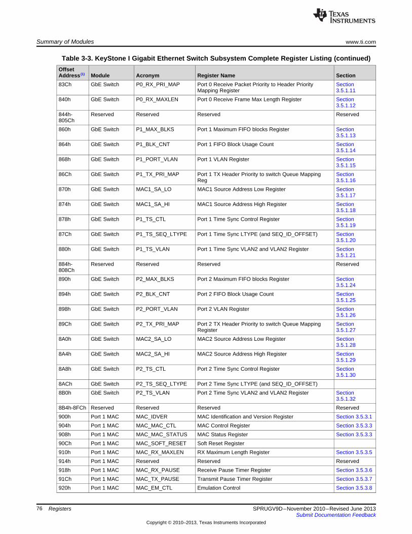
Summary of Modules www.ti.com
76 SPRUGV9D–November 2010–Revised June 2013Submit Documentation Feedback
Copyright © 2010–2013, Texas Instruments Incorporated
Registers
Table 3-3. KeyStone I Gigabit Ethernet Switch Subsystem Complete Register Listing (continued)OffsetAddress (1) Module Acronym Register Name Section83Ch GbE Switch P0_RX_PRI_MAP Port 0 Receive Packet Priority to Header Priority
Mapping RegisterSection3.5.1.11
840h GbE Switch P0_RX_MAXLEN Port 0 Receive Frame Max Length Register Section3.5.1.12
844h-805Ch
Reserved Reserved Reserved Reserved
860h GbE Switch P1_MAX_BLKS Port 1 Maximum FIFO blocks Register Section3.5.1.13
864h GbE Switch P1_BLK_CNT Port 1 FIFO Block Usage Count Section3.5.1.14
868h GbE Switch P1_PORT_VLAN Port 1 VLAN Register Section3.5.1.15
86Ch GbE Switch P1_TX_PRI_MAP Port 1 TX Header Priority to switch Queue MappingReg
Section3.5.1.16
870h GbE Switch MAC1_SA_LO MAC1 Source Address Low Register Section3.5.1.17
874h GbE Switch MAC1_SA_HI MAC1 Source Address High Register Section3.5.1.18
878h GbE Switch P1_TS_CTL Port 1 Time Sync Control Register Section3.5.1.19
87Ch GbE Switch P1_TS_SEQ_LTYPE Port 1 Time Sync LTYPE (and SEQ_ID_OFFSET) Section3.5.1.20
880h GbE Switch P1_TS_VLAN Port 1 Time Sync VLAN2 and VLAN2 Register Section3.5.1.21
884h-808Ch
Reserved Reserved Reserved Reserved
890h GbE Switch P2_MAX_BLKS Port 2 Maximum FIFO blocks Register Section3.5.1.24
894h GbE Switch P2_BLK_CNT Port 2 FIFO Block Usage Count Section3.5.1.25
898h GbE Switch P2_PORT_VLAN Port 2 VLAN Register Section3.5.1.26
89Ch GbE Switch P2_TX_PRI_MAP Port 2 TX Header Priority to switch Queue MappingRegister
Section3.5.1.27
8A0h GbE Switch MAC2_SA_LO MAC2 Source Address Low Register Section3.5.1.28
8A4h GbE Switch MAC2_SA_HI MAC2 Source Address High Register Section3.5.1.29
8A8h GbE Switch P2_TS_CTL Port 2 Time Sync Control Register Section3.5.1.30
8ACh GbE Switch P2_TS_SEQ_LTYPE Port 2 Time Sync LTYPE (and SEQ_ID_OFFSET)8B0h GbE Switch P2_TS_VLAN Port 2 Time Sync VLAN2 and VLAN2 Register Section
3.5.1.328B4h-8FCh Reserved Reserved Reserved Reserved900h Port 1 MAC MAC_IDVER MAC Identification and Version Register Section 3.5.3.1904h Port 1 MAC MAC_MAC_CTL MAC Control Register Section 3.5.3.3908h Port 1 MAC MAC_MAC_STATUS MAC Status Register Section 3.5.3.390Ch Port 1 MAC MAC_SOFT_RESET Soft Reset Register910h Port 1 MAC MAC_RX_MAXLEN RX Maximum Length Register Section 3.5.3.5914h Port 1 MAC Reserved Reserved Reserved918h Port 1 MAC MAC_RX_PAUSE Receive Pause Timer Register Section 3.5.3.691Ch Port 1 MAC MAC_TX_PAUSE Transmit Pause Timer Register Section 3.5.3.7920h Port 1 MAC MAC_EM_CTL Emulation Control Section 3.5.3.8
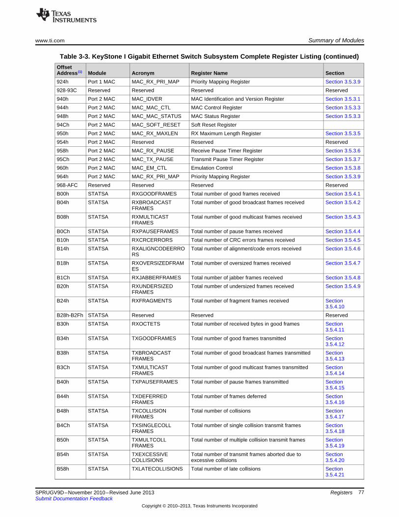
www.ti.com Summary of Modules
77SPRUGV9D–November 2010–Revised June 2013Submit Documentation Feedback
Copyright © 2010–2013, Texas Instruments Incorporated
Registers
Table 3-3. KeyStone I Gigabit Ethernet Switch Subsystem Complete Register Listing (continued)OffsetAddress (1) Module Acronym Register Name Section924h Port 1 MAC MAC_RX_PRI_MAP Priority Mapping Register Section 3.5.3.9928-93C Reserved Reserved Reserved Reserved940h Port 2 MAC MAC_IDVER MAC Identification and Version Register Section 3.5.3.1944h Port 2 MAC MAC_MAC_CTL MAC Control Register Section 3.5.3.3948h Port 2 MAC MAC_MAC_STATUS MAC Status Register Section 3.5.3.394Ch Port 2 MAC MAC_SOFT_RESET Soft Reset Register950h Port 2 MAC MAC_RX_MAXLEN RX Maximum Length Register Section 3.5.3.5954h Port 2 MAC Reserved Reserved Reserved958h Port 2 MAC MAC_RX_PAUSE Receive Pause Timer Register Section 3.5.3.695Ch Port 2 MAC MAC_TX_PAUSE Transmit Pause Timer Register Section 3.5.3.7960h Port 2 MAC MAC_EM_CTL Emulation Control Section 3.5.3.8964h Port 2 MAC MAC_RX_PRI_MAP Priority Mapping Register Section 3.5.3.9968-AFC Reserved Reserved Reserved ReservedB00h STATSA RXGOODFRAMES Total number of good frames received Section 3.5.4.1B04h STATSA RXBROADCAST
FRAMESTotal number of good broadcast frames received Section 3.5.4.2
B08h STATSA RXMULTICASTFRAMES
Total number of good multicast frames received Section 3.5.4.3
B0Ch STATSA RXPAUSEFRAMES Total number of pause frames received Section 3.5.4.4B10h STATSA RXCRCERRORS Total number of CRC errors frames received Section 3.5.4.5B14h STATSA RXALIGNCODEERRO
RSTotal number of alignment/code errors received Section 3.5.4.6
B18h STATSA RXOVERSIZEDFRAMES
Total number of oversized frames received Section 3.5.4.7
B1Ch STATSA RXJABBERFRAMES Total number of jabber frames received Section 3.5.4.8B20h STATSA RXUNDERSIZED
FRAMESTotal number of undersized frames received Section 3.5.4.9
B24h STATSA RXFRAGMENTS Total number of fragment frames received Section3.5.4.10
B28h-B2Fh STATSA Reserved Reserved ReservedB30h STATSA RXOCTETS Total number of received bytes in good frames Section
3.5.4.11B34h STATSA TXGOODFRAMES Total number of good frames transmitted Section
3.5.4.12B38h STATSA TXBROADCAST
FRAMESTotal number of good broadcast frames transmitted Section
3.5.4.13B3Ch STATSA TXMULTICAST
FRAMESTotal number of good multicast frames transmitted Section
3.5.4.14B40h STATSA TXPAUSEFRAMES Total number of pause frames transmitted Section
3.5.4.15B44h STATSA TXDEFERRED
FRAMESTotal number of frames deferred Section
3.5.4.16B48h STATSA TXCOLLISION
FRAMESTotal number of collisions Section
3.5.4.17B4Ch STATSA TXSINGLECOLL
FRAMESTotal number of single collision transmit frames Section
3.5.4.18B50h STATSA TXMULTCOLL
FRAMESTotal number of multiple collision transmit frames Section
3.5.4.19B54h STATSA TXEXCESSIVE
COLLISIONSTotal number of transmit frames aborted due toexcessive collisions
Section3.5.4.20
B58h STATSA TXLATECOLLISIONS Total number of late collisions Section3.5.4.21
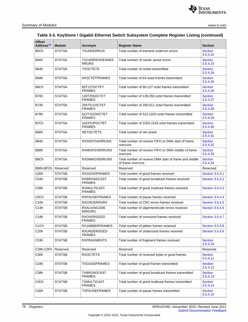
Summary of Modules www.ti.com
78 SPRUGV9D–November 2010–Revised June 2013Submit Documentation Feedback
Copyright © 2010–2013, Texas Instruments Incorporated
Registers
Table 3-3. KeyStone I Gigabit Ethernet Switch Subsystem Complete Register Listing (continued)OffsetAddress (1) Module Acronym Register Name SectionB5Ch STATSA TXUNDERRUN Total number of transmit underrun errors Section
3.5.4.22B60h STATSA TXCARRIERSENSEE
RRORSTotal number of carrier sense errors Section
3.5.4.23B64h STATSA TXOCTETS Total number of octets transmitted Section
3.5.4.24B68h STATSA 64OCTETFRAMES Total number of 64 octet frames transmitted Section
3.5.4.25B6Ch STATSA 65T127OCTET
FRAMESTotal number of 65-127 octet frames transmitted Section
3.5.4.26B70h STATSA 128T255OCTET
FRAMESTotal number of 128-255 octet frames transmitted Section
3.5.4.27B74h STATSA 256T511OCTET
FRAMESTotal number of 256-511 octet frames transmitted Section
3.5.4.28B78h STATSA 512T1023OCTET
FRAMESTotal number of 512-1023 octet frames transmitted Section
3.5.4.29B7Ch STATSA 1024TUPOCTET
FRAMESTotal number of 1023-1518 octet frames transmitted Section
3.5.4.30B80h STATSA NETOCTETS Total number of net octets Section
3.5.4.31B84h STATSA RXSOFOVERRUNS Total number of receive FIFO or DMA start of frame
overrunsSection3.5.4.32
B88h STATSA RXMOFOVERRUNS Total number of receive FIFO or DMA middle of frameoverruns
Section3.5.4.33
B8Ch STATSA RXDMAOVERRUNS Total number of receive DMA start of frame and middleof frame overruns
Section3.5.4.34
B90h-BFCh Reserved Reserved Reserved ReservedC00h STATSB RXGOODFRAMES Total number of good frames received Section 3.5.4.1C04h STATSB RXBROADCAST
FRAMESTotal number of good broadcast frames received Section 3.5.4.2
C08h STATSB RXMULTICASTFRAMES
Total number of good multicast frames received Section 3.5.4.3
C0Ch STATSB RXPAUSEFRAMES Total number of pause frames received Section 3.5.4.4C10h STATSB RXCRCERRORS Total number of CRC errors frames received Section 3.5.4.5C14h STATSB RXALIGNCODE
ERRORSTotal number of alignment/code errors received Section 3.5.4.6
C18h STATSB RXOVERSIZEDFRAMES
Total number of oversized frames received Section 3.5.4.7
C1Ch STATSB RXJABBERFRAMES Total number of jabber frames received Section 3.5.4.8C20h STATSB RXUNDERSIZED
FRAMESTotal number of undersized frames received Section 3.5.4.9
C24h STATSB RXFRAGMENTS Total number of fragment frames received Section3.5.4.10
C28h-C2Fh Reserved Reserved Reserved ReservedC30h STATSB RXOCTETS Total number of received bytes in good frames Section
3.5.4.11C34h STATSB TXGOODFRAMES Total number of good frames transmitted Section
3.5.4.12C38h STATSB TXBROADCAST
FRAMESTotal number of good broadcast frames transmitted Section
3.5.4.13C3Ch STATSB TXMULTICAST
FRAMESTotal number of good multicast frames transmitted Section
3.5.4.14C40h STATSB TXPAUSEFRAMES Total number of pause frames transmitted Section
3.5.4.15
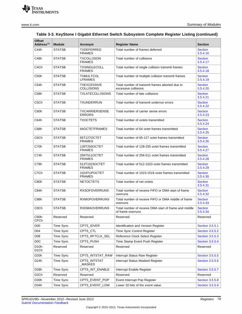
www.ti.com Summary of Modules
79SPRUGV9D–November 2010–Revised June 2013Submit Documentation Feedback
Copyright © 2010–2013, Texas Instruments Incorporated
Registers
Table 3-3. KeyStone I Gigabit Ethernet Switch Subsystem Complete Register Listing (continued)OffsetAddress (1) Module Acronym Register Name SectionC44h STATSB TXDEFERRED
FRAMESTotal number of frames deferred Section
3.5.4.16C48h STATSB TXCOLLISION
FRAMESTotal number of collisions Section
3.5.4.17C4Ch STATSB TXSINGLECOLL
FRAMESTotal number of single collision transmit frames Section
3.5.4.18C50h STATSB TXMULTCOL
LFRAMESTotal number of multiple collision transmit frames Section
3.5.4.19C54h STATSB TXEXCESSIVE
COLLISIONSTotal number of transmit frames aborted due toexcessive collisions
Section3.5.4.20
C58h STATSB TXLATECOLLISIONS Total number of late collisions Section3.5.4.21
C5Ch STATSB TXUNDERRUN Total number of transmit underrun errors Section3.5.4.22
C60h STATSB TXCARRIERSENSEERRORS
Total number of carrier sense errors Section3.5.4.23
C64h STATSB TXOCTETS Total number of octets transmitted Section3.5.4.24
C68h STATSB 64OCTETFRAMES Total number of 64 octet frames transmitted Section3.5.4.25
C6Ch STATSB 65T127OCTETFRAMES
Total number of 65-127 octet frames transmitted Section3.5.4.26
C70h STATSB 128T255OCTETFRAMES
Total number of 128-255 octet frames transmitted Section3.5.4.27
C74h STATSB 256T511OCTETFRAMES
Total number of 256-511 octet frames transmitted Section3.5.4.28
C78h STATSB 512T1023OCTETFRAMES
Total number of 512-1023 octet frames transmitted Section3.5.4.29
C7Ch STATSB 1024TUPOCTETFRAMES
Total number of 1023-1518 octet frames transmitted Section3.5.4.30
C80h STATSB NETOCTETS Total number of net octets Section3.5.4.31
C84h STATSB RXSOFOVERRUNS Total number of receive FIFO or DMA start of frameoverruns
Section3.5.4.32
C88h STATSB RXMOFOVERRUNS Total number of receive FIFO or DMA middle of frameoverruns
Section3.5.4.33
C8Ch STATSB RXDMAOVERRUNS Total number of receive DMA start of frame and middleof frame overruns
Section3.5.4.34
C90h-CFCh
Reserved Reserved Reserved Reserved
D00 Time Sync CPTS_IDVER Identification and Version Register Section 3.5.5.1D04 Time Sync CPTS_CTL Time Sync Control Register Section 3.5.5.2D08 Time Sync CPTS_RFTCLK_SEL Reference Clock Select Register Section 3.5.5.3D0C Time Sync CPTS_PUSH Time Stamp Event Push Register Section 3.5.5.4D10h-D1Ch
Reserved Reserved Reserved Reserved
D20h Time Sync CPTS_INTSTAT_RAW Interrupt Status Raw Register Section 3.5.5.5D24h Time Sync CPTS_INTSTAT
_MASKEDInterrupt Status Masked Register Section 3.5.5.6
D28h Time Sync CPTS_INT_ENABLE Interrupt Enable Register Section 3.5.5.7D2Ch Reserved Reserved Reserved ReservedD30h Time Sync CPTS_EVENT_POP Event Interrupt Pop Register Section 3.5.5.8D34h Time Sync CPTS_EVENT_LOW Lower 32-bits of the event value Section 3.5.5.9
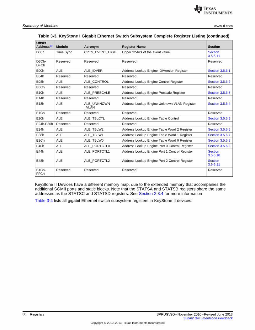
Summary of Modules www.ti.com
80 SPRUGV9D–November 2010–Revised June 2013Submit Documentation Feedback
Copyright © 2010–2013, Texas Instruments Incorporated
Registers
Table 3-3. KeyStone I Gigabit Ethernet Switch Subsystem Complete Register Listing (continued)OffsetAddress (1) Module Acronym Register Name SectionD38h Time Sync CPTS_EVENT_HIGH Upper 32-bits of the event value Section
3.5.5.11D3Ch-DFCh
Reserved Reserved Reserved Reserved
E00h ALE ALE_IDVER Address Lookup Engine ID/Version Register Section 3.5.6.1E04h Reserved Reserved Reserved ReservedE08h ALE ALE_CONTROL Address Lookup Engine Control Register Section 3.5.6.2E0Ch Reserved Reserved Reserved ReservedE10h ALE ALE_PRESCALE Address Lookup Engine Prescale Register Section 3.5.6.3E14h Reserved Reserved Reserved ReservedE18h ALE ALE_UNKNOWN
_VLANAddress Lookup Engine Unknown VLAN Register Section 3.5.6.4
E1Ch Reserved Reserved Reserved ReservedE20h ALE ALE_TBLCTL Address Lookup Engine Table Control Section 3.5.6.5E24h-E30h Reserved Reserved Reserved ReservedE34h ALE ALE_TBLW2 Address Lookup Engine Table Word 2 Register Section 3.5.6.6E38h ALE ALE_TBLW1 Address Lookup Engine Table Word 1 Register Section 3.5.6.7E3Ch ALE ALE_TBLW0 Address Lookup Engine Table Word 0 Register Section 3.5.6.8E40h ALE ALE_PORTCTL0 Address Lookup Engine Port 0 Control Register Section 3.5.6.9E44h ALE ALE_PORTCTL1 Address Lookup Engine Port 1 Control Register Section
3.5.6.10E48h ALE ALE_PORTCTL2 Address Lookup Engine Port 2 Control Register Section
3.5.6.11E4Ch-FFCh
Reserved Reserved Reserved Reserved
KeyStone II Devices have a different memory map, due to the extended memory that accompanies theadditional SGMII ports and static blocks. Note that the STATSA and STATSB registers share the sameaddresses as the STATSC and STATSD registers. See Section 2.3.4 for more information
Table 3-4 lists all gigabit Ethernet switch subsystem registers in KeyStone II devices.
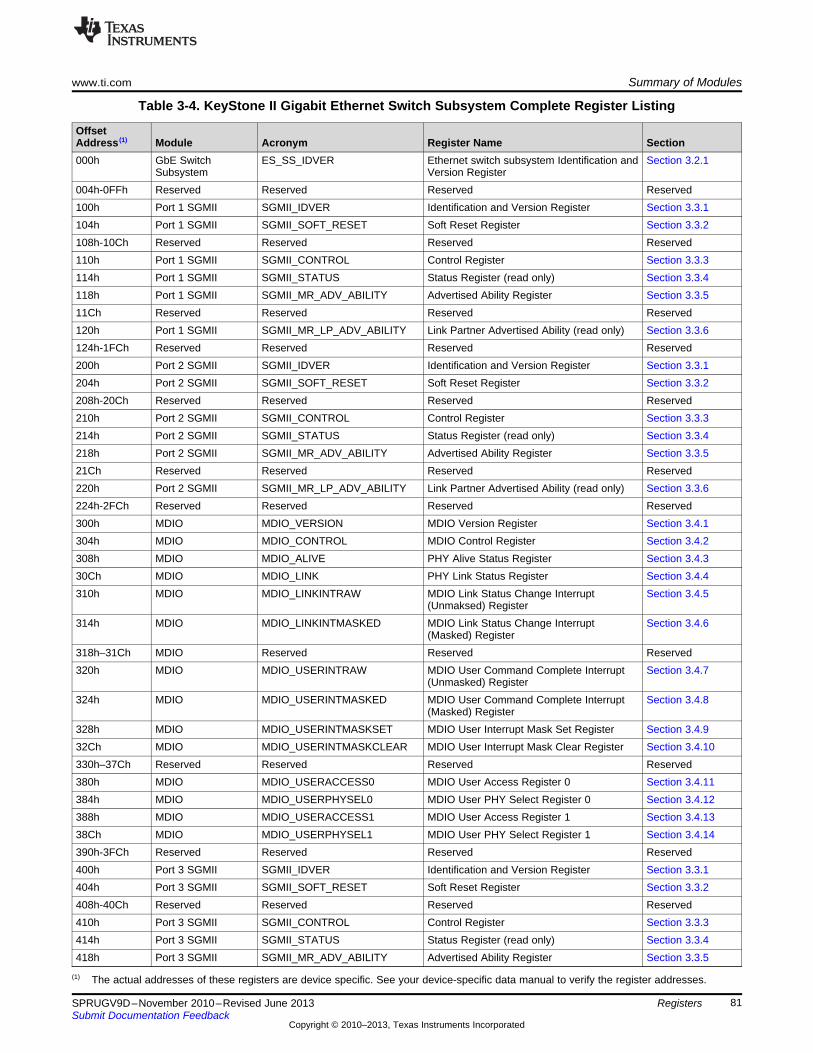
www.ti.com Summary of Modules
81SPRUGV9D–November 2010–Revised June 2013Submit Documentation Feedback
Copyright © 2010–2013, Texas Instruments Incorporated
Registers
(1) The actual addresses of these registers are device specific. See your device-specific data manual to verify the register addresses.
Table 3-4. KeyStone II Gigabit Ethernet Switch Subsystem Complete Register Listing
OffsetAddress (1) Module Acronym Register Name Section000h GbE Switch
SubsystemES_SS_IDVER Ethernet switch subsystem Identification and
Version RegisterSection 3.2.1
004h-0FFh Reserved Reserved Reserved Reserved100h Port 1 SGMII SGMII_IDVER Identification and Version Register Section 3.3.1104h Port 1 SGMII SGMII_SOFT_RESET Soft Reset Register Section 3.3.2108h-10Ch Reserved Reserved Reserved Reserved110h Port 1 SGMII SGMII_CONTROL Control Register Section 3.3.3114h Port 1 SGMII SGMII_STATUS Status Register (read only) Section 3.3.4118h Port 1 SGMII SGMII_MR_ADV_ABILITY Advertised Ability Register Section 3.3.511Ch Reserved Reserved Reserved Reserved120h Port 1 SGMII SGMII_MR_LP_ADV_ABILITY Link Partner Advertised Ability (read only) Section 3.3.6124h-1FCh Reserved Reserved Reserved Reserved200h Port 2 SGMII SGMII_IDVER Identification and Version Register Section 3.3.1204h Port 2 SGMII SGMII_SOFT_RESET Soft Reset Register Section 3.3.2208h-20Ch Reserved Reserved Reserved Reserved210h Port 2 SGMII SGMII_CONTROL Control Register Section 3.3.3214h Port 2 SGMII SGMII_STATUS Status Register (read only) Section 3.3.4218h Port 2 SGMII SGMII_MR_ADV_ABILITY Advertised Ability Register Section 3.3.521Ch Reserved Reserved Reserved Reserved220h Port 2 SGMII SGMII_MR_LP_ADV_ABILITY Link Partner Advertised Ability (read only) Section 3.3.6224h-2FCh Reserved Reserved Reserved Reserved300h MDIO MDIO_VERSION MDIO Version Register Section 3.4.1304h MDIO MDIO_CONTROL MDIO Control Register Section 3.4.2308h MDIO MDIO_ALIVE PHY Alive Status Register Section 3.4.330Ch MDIO MDIO_LINK PHY Link Status Register Section 3.4.4310h MDIO MDIO_LINKINTRAW MDIO Link Status Change Interrupt
(Unmaksed) RegisterSection 3.4.5
314h MDIO MDIO_LINKINTMASKED MDIO Link Status Change Interrupt(Masked) Register
Section 3.4.6
318h–31Ch MDIO Reserved Reserved Reserved320h MDIO MDIO_USERINTRAW MDIO User Command Complete Interrupt
(Unmasked) RegisterSection 3.4.7
324h MDIO MDIO_USERINTMASKED MDIO User Command Complete Interrupt(Masked) Register
Section 3.4.8
328h MDIO MDIO_USERINTMASKSET MDIO User Interrupt Mask Set Register Section 3.4.932Ch MDIO MDIO_USERINTMASKCLEAR MDIO User Interrupt Mask Clear Register Section 3.4.10330h–37Ch Reserved Reserved Reserved Reserved380h MDIO MDIO_USERACCESS0 MDIO User Access Register 0 Section 3.4.11384h MDIO MDIO_USERPHYSEL0 MDIO User PHY Select Register 0 Section 3.4.12388h MDIO MDIO_USERACCESS1 MDIO User Access Register 1 Section 3.4.1338Ch MDIO MDIO_USERPHYSEL1 MDIO User PHY Select Register 1 Section 3.4.14390h-3FCh Reserved Reserved Reserved Reserved400h Port 3 SGMII SGMII_IDVER Identification and Version Register Section 3.3.1404h Port 3 SGMII SGMII_SOFT_RESET Soft Reset Register Section 3.3.2408h-40Ch Reserved Reserved Reserved Reserved410h Port 3 SGMII SGMII_CONTROL Control Register Section 3.3.3414h Port 3 SGMII SGMII_STATUS Status Register (read only) Section 3.3.4418h Port 3 SGMII SGMII_MR_ADV_ABILITY Advertised Ability Register Section 3.3.5
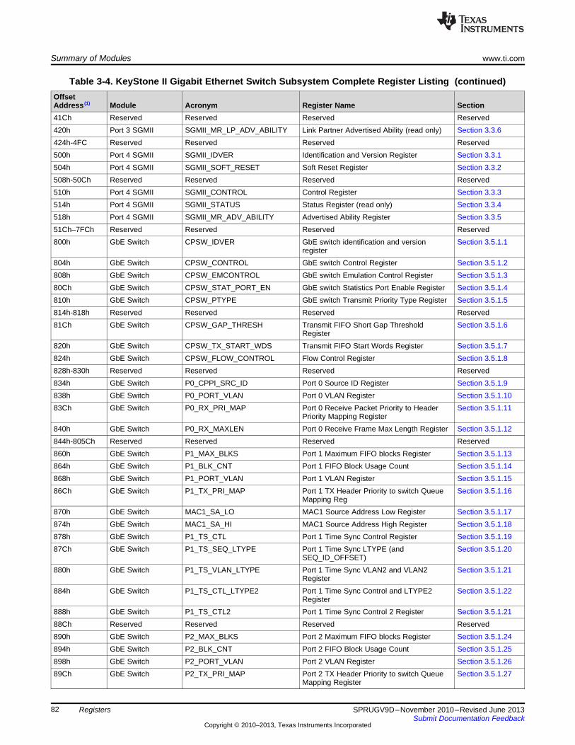
Summary of Modules www.ti.com
82 SPRUGV9D–November 2010–Revised June 2013Submit Documentation Feedback
Copyright © 2010–2013, Texas Instruments Incorporated
Registers
Table 3-4. KeyStone II Gigabit Ethernet Switch Subsystem Complete Register Listing (continued)OffsetAddress (1) Module Acronym Register Name Section41Ch Reserved Reserved Reserved Reserved420h Port 3 SGMII SGMII_MR_LP_ADV_ABILITY Link Partner Advertised Ability (read only) Section 3.3.6424h-4FC Reserved Reserved Reserved Reserved500h Port 4 SGMII SGMII_IDVER Identification and Version Register Section 3.3.1504h Port 4 SGMII SGMII_SOFT_RESET Soft Reset Register Section 3.3.2508h-50Ch Reserved Reserved Reserved Reserved510h Port 4 SGMII SGMII_CONTROL Control Register Section 3.3.3514h Port 4 SGMII SGMII_STATUS Status Register (read only) Section 3.3.4518h Port 4 SGMII SGMII_MR_ADV_ABILITY Advertised Ability Register Section 3.3.551Ch–7FCh Reserved Reserved Reserved Reserved800h GbE Switch CPSW_IDVER GbE switch identification and version
registerSection 3.5.1.1
804h GbE Switch CPSW_CONTROL GbE switch Control Register Section 3.5.1.2808h GbE Switch CPSW_EMCONTROL GbE switch Emulation Control Register Section 3.5.1.380Ch GbE Switch CPSW_STAT_PORT_EN GbE switch Statistics Port Enable Register Section 3.5.1.4810h GbE Switch CPSW_PTYPE GbE switch Transmit Priority Type Register Section 3.5.1.5814h-818h Reserved Reserved Reserved Reserved81Ch GbE Switch CPSW_GAP_THRESH Transmit FIFO Short Gap Threshold
RegisterSection 3.5.1.6
820h GbE Switch CPSW_TX_START_WDS Transmit FIFO Start Words Register Section 3.5.1.7824h GbE Switch CPSW_FLOW_CONTROL Flow Control Register Section 3.5.1.8828h-830h Reserved Reserved Reserved Reserved834h GbE Switch P0_CPPI_SRC_ID Port 0 Source ID Register Section 3.5.1.9838h GbE Switch P0_PORT_VLAN Port 0 VLAN Register Section 3.5.1.1083Ch GbE Switch P0_RX_PRI_MAP Port 0 Receive Packet Priority to Header
Priority Mapping RegisterSection 3.5.1.11
840h GbE Switch P0_RX_MAXLEN Port 0 Receive Frame Max Length Register Section 3.5.1.12844h-805Ch Reserved Reserved Reserved Reserved860h GbE Switch P1_MAX_BLKS Port 1 Maximum FIFO blocks Register Section 3.5.1.13864h GbE Switch P1_BLK_CNT Port 1 FIFO Block Usage Count Section 3.5.1.14868h GbE Switch P1_PORT_VLAN Port 1 VLAN Register Section 3.5.1.1586Ch GbE Switch P1_TX_PRI_MAP Port 1 TX Header Priority to switch Queue
Mapping RegSection 3.5.1.16
870h GbE Switch MAC1_SA_LO MAC1 Source Address Low Register Section 3.5.1.17874h GbE Switch MAC1_SA_HI MAC1 Source Address High Register Section 3.5.1.18878h GbE Switch P1_TS_CTL Port 1 Time Sync Control Register Section 3.5.1.1987Ch GbE Switch P1_TS_SEQ_LTYPE Port 1 Time Sync LTYPE (and
SEQ_ID_OFFSET)Section 3.5.1.20
880h GbE Switch P1_TS_VLAN_LTYPE Port 1 Time Sync VLAN2 and VLAN2Register
Section 3.5.1.21
884h GbE Switch P1_TS_CTL_LTYPE2 Port 1 Time Sync Control and LTYPE2Register
Section 3.5.1.22
888h GbE Switch P1_TS_CTL2 Port 1 Time Sync Control 2 Register Section 3.5.1.2188Ch Reserved Reserved Reserved Reserved890h GbE Switch P2_MAX_BLKS Port 2 Maximum FIFO blocks Register Section 3.5.1.24894h GbE Switch P2_BLK_CNT Port 2 FIFO Block Usage Count Section 3.5.1.25898h GbE Switch P2_PORT_VLAN Port 2 VLAN Register Section 3.5.1.2689Ch GbE Switch P2_TX_PRI_MAP Port 2 TX Header Priority to switch Queue
Mapping RegisterSection 3.5.1.27
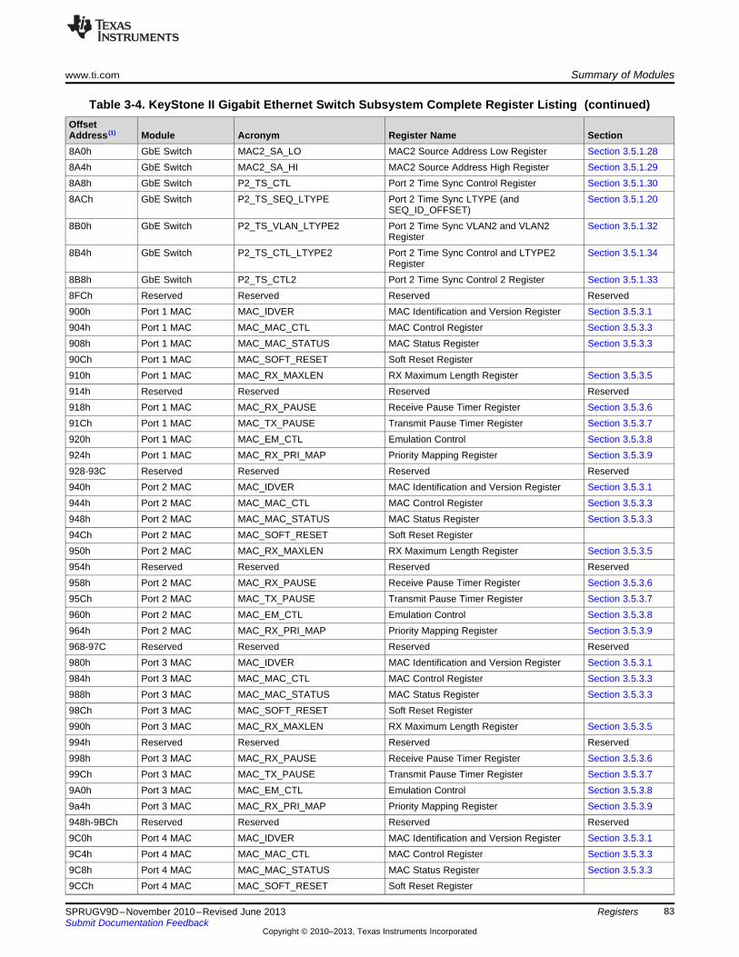
www.ti.com Summary of Modules
83SPRUGV9D–November 2010–Revised June 2013Submit Documentation Feedback
Copyright © 2010–2013, Texas Instruments Incorporated
Registers
Table 3-4. KeyStone II Gigabit Ethernet Switch Subsystem Complete Register Listing (continued)OffsetAddress (1) Module Acronym Register Name Section8A0h GbE Switch MAC2_SA_LO MAC2 Source Address Low Register Section 3.5.1.288A4h GbE Switch MAC2_SA_HI MAC2 Source Address High Register Section 3.5.1.298A8h GbE Switch P2_TS_CTL Port 2 Time Sync Control Register Section 3.5.1.308ACh GbE Switch P2_TS_SEQ_LTYPE Port 2 Time Sync LTYPE (and
SEQ_ID_OFFSET)Section 3.5.1.20
8B0h GbE Switch P2_TS_VLAN_LTYPE2 Port 2 Time Sync VLAN2 and VLAN2Register
Section 3.5.1.32
8B4h GbE Switch P2_TS_CTL_LTYPE2 Port 2 Time Sync Control and LTYPE2Register
Section 3.5.1.34
8B8h GbE Switch P2_TS_CTL2 Port 2 Time Sync Control 2 Register Section 3.5.1.338FCh Reserved Reserved Reserved Reserved900h Port 1 MAC MAC_IDVER MAC Identification and Version Register Section 3.5.3.1904h Port 1 MAC MAC_MAC_CTL MAC Control Register Section 3.5.3.3908h Port 1 MAC MAC_MAC_STATUS MAC Status Register Section 3.5.3.390Ch Port 1 MAC MAC_SOFT_RESET Soft Reset Register910h Port 1 MAC MAC_RX_MAXLEN RX Maximum Length Register Section 3.5.3.5914h Reserved Reserved Reserved Reserved918h Port 1 MAC MAC_RX_PAUSE Receive Pause Timer Register Section 3.5.3.691Ch Port 1 MAC MAC_TX_PAUSE Transmit Pause Timer Register Section 3.5.3.7920h Port 1 MAC MAC_EM_CTL Emulation Control Section 3.5.3.8924h Port 1 MAC MAC_RX_PRI_MAP Priority Mapping Register Section 3.5.3.9928-93C Reserved Reserved Reserved Reserved940h Port 2 MAC MAC_IDVER MAC Identification and Version Register Section 3.5.3.1944h Port 2 MAC MAC_MAC_CTL MAC Control Register Section 3.5.3.3948h Port 2 MAC MAC_MAC_STATUS MAC Status Register Section 3.5.3.394Ch Port 2 MAC MAC_SOFT_RESET Soft Reset Register950h Port 2 MAC MAC_RX_MAXLEN RX Maximum Length Register Section 3.5.3.5954h Reserved Reserved Reserved Reserved958h Port 2 MAC MAC_RX_PAUSE Receive Pause Timer Register Section 3.5.3.695Ch Port 2 MAC MAC_TX_PAUSE Transmit Pause Timer Register Section 3.5.3.7960h Port 2 MAC MAC_EM_CTL Emulation Control Section 3.5.3.8964h Port 2 MAC MAC_RX_PRI_MAP Priority Mapping Register Section 3.5.3.9968-97C Reserved Reserved Reserved Reserved980h Port 3 MAC MAC_IDVER MAC Identification and Version Register Section 3.5.3.1984h Port 3 MAC MAC_MAC_CTL MAC Control Register Section 3.5.3.3988h Port 3 MAC MAC_MAC_STATUS MAC Status Register Section 3.5.3.398Ch Port 3 MAC MAC_SOFT_RESET Soft Reset Register990h Port 3 MAC MAC_RX_MAXLEN RX Maximum Length Register Section 3.5.3.5994h Reserved Reserved Reserved Reserved998h Port 3 MAC MAC_RX_PAUSE Receive Pause Timer Register Section 3.5.3.699Ch Port 3 MAC MAC_TX_PAUSE Transmit Pause Timer Register Section 3.5.3.79A0h Port 3 MAC MAC_EM_CTL Emulation Control Section 3.5.3.89a4h Port 3 MAC MAC_RX_PRI_MAP Priority Mapping Register Section 3.5.3.9948h-9BCh Reserved Reserved Reserved Reserved9C0h Port 4 MAC MAC_IDVER MAC Identification and Version Register Section 3.5.3.19C4h Port 4 MAC MAC_MAC_CTL MAC Control Register Section 3.5.3.39C8h Port 4 MAC MAC_MAC_STATUS MAC Status Register Section 3.5.3.39CCh Port 4 MAC MAC_SOFT_RESET Soft Reset Register
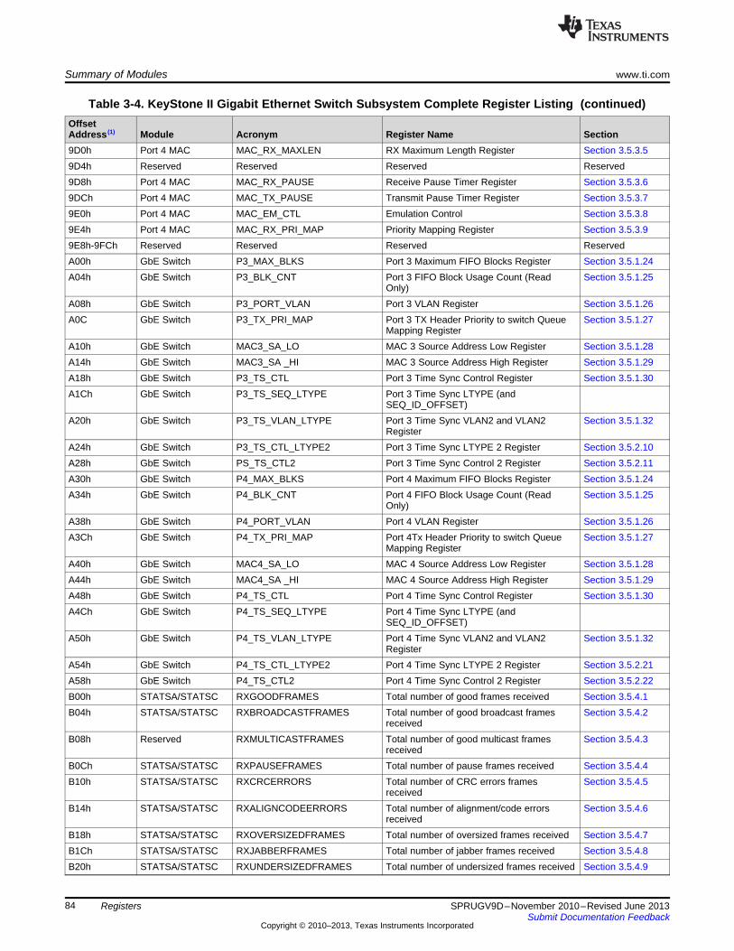
Summary of Modules www.ti.com
84 SPRUGV9D–November 2010–Revised June 2013Submit Documentation Feedback
Copyright © 2010–2013, Texas Instruments Incorporated
Registers
Table 3-4. KeyStone II Gigabit Ethernet Switch Subsystem Complete Register Listing (continued)OffsetAddress (1) Module Acronym Register Name Section9D0h Port 4 MAC MAC_RX_MAXLEN RX Maximum Length Register Section 3.5.3.59D4h Reserved Reserved Reserved Reserved9D8h Port 4 MAC MAC_RX_PAUSE Receive Pause Timer Register Section 3.5.3.69DCh Port 4 MAC MAC_TX_PAUSE Transmit Pause Timer Register Section 3.5.3.79E0h Port 4 MAC MAC_EM_CTL Emulation Control Section 3.5.3.89E4h Port 4 MAC MAC_RX_PRI_MAP Priority Mapping Register Section 3.5.3.99E8h-9FCh Reserved Reserved Reserved ReservedA00h GbE Switch P3_MAX_BLKS Port 3 Maximum FIFO Blocks Register Section 3.5.1.24A04h GbE Switch P3_BLK_CNT Port 3 FIFO Block Usage Count (Read
Only)Section 3.5.1.25
A08h GbE Switch P3_PORT_VLAN Port 3 VLAN Register Section 3.5.1.26A0C GbE Switch P3_TX_PRI_MAP Port 3 TX Header Priority to switch Queue
Mapping RegisterSection 3.5.1.27
A10h GbE Switch MAC3_SA_LO MAC 3 Source Address Low Register Section 3.5.1.28A14h GbE Switch MAC3_SA _HI MAC 3 Source Address High Register Section 3.5.1.29A18h GbE Switch P3_TS_CTL Port 3 Time Sync Control Register Section 3.5.1.30A1Ch GbE Switch P3_TS_SEQ_LTYPE Port 3 Time Sync LTYPE (and
SEQ_ID_OFFSET)A20h GbE Switch P3_TS_VLAN_LTYPE Port 3 Time Sync VLAN2 and VLAN2
RegisterSection 3.5.1.32
A24h GbE Switch P3_TS_CTL_LTYPE2 Port 3 Time Sync LTYPE 2 Register Section 3.5.2.10A28h GbE Switch PS_TS_CTL2 Port 3 Time Sync Control 2 Register Section 3.5.2.11A30h GbE Switch P4_MAX_BLKS Port 4 Maximum FIFO Blocks Register Section 3.5.1.24A34h GbE Switch P4_BLK_CNT Port 4 FIFO Block Usage Count (Read
Only)Section 3.5.1.25
A38h GbE Switch P4_PORT_VLAN Port 4 VLAN Register Section 3.5.1.26A3Ch GbE Switch P4_TX_PRI_MAP Port 4Tx Header Priority to switch Queue
Mapping RegisterSection 3.5.1.27
A40h GbE Switch MAC4_SA_LO MAC 4 Source Address Low Register Section 3.5.1.28A44h GbE Switch MAC4_SA _HI MAC 4 Source Address High Register Section 3.5.1.29A48h GbE Switch P4_TS_CTL Port 4 Time Sync Control Register Section 3.5.1.30A4Ch GbE Switch P4_TS_SEQ_LTYPE Port 4 Time Sync LTYPE (and
SEQ_ID_OFFSET)A50h GbE Switch P4_TS_VLAN_LTYPE Port 4 Time Sync VLAN2 and VLAN2
RegisterSection 3.5.1.32
A54h GbE Switch P4_TS_CTL_LTYPE2 Port 4 Time Sync LTYPE 2 Register Section 3.5.2.21A58h GbE Switch P4_TS_CTL2 Port 4 Time Sync Control 2 Register Section 3.5.2.22B00h STATSA/STATSC RXGOODFRAMES Total number of good frames received Section 3.5.4.1B04h STATSA/STATSC RXBROADCASTFRAMES Total number of good broadcast frames
receivedSection 3.5.4.2
B08h Reserved RXMULTICASTFRAMES Total number of good multicast framesreceived
Section 3.5.4.3
B0Ch STATSA/STATSC RXPAUSEFRAMES Total number of pause frames received Section 3.5.4.4B10h STATSA/STATSC RXCRCERRORS Total number of CRC errors frames
receivedSection 3.5.4.5
B14h STATSA/STATSC RXALIGNCODEERRORS Total number of alignment/code errorsreceived
Section 3.5.4.6
B18h STATSA/STATSC RXOVERSIZEDFRAMES Total number of oversized frames received Section 3.5.4.7B1Ch STATSA/STATSC RXJABBERFRAMES Total number of jabber frames received Section 3.5.4.8B20h STATSA/STATSC RXUNDERSIZEDFRAMES Total number of undersized frames received Section 3.5.4.9
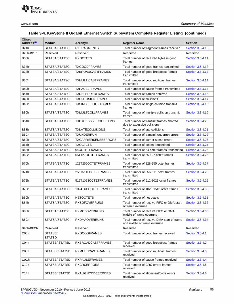
www.ti.com Summary of Modules
85SPRUGV9D–November 2010–Revised June 2013Submit Documentation Feedback
Copyright © 2010–2013, Texas Instruments Incorporated
Registers
Table 3-4. KeyStone II Gigabit Ethernet Switch Subsystem Complete Register Listing (continued)OffsetAddress (1) Module Acronym Register Name SectionB24h STATSA/STATSC RXFRAGMENTS Total number of fragment frames received Section 3.5.4.10B28h-B2Fh Reserved Reserved Reserved ReservedB30h STATSA/STATSC RXOCTETS Total number of received bytes in good
framesSection 3.5.4.11
B34h STATSA/STATSC TXGOODFRAMES Total number of good frames transmitted Section 3.5.4.12B38h STATSA/STATSC TXBROADCASTFRAMES Total number of good broadcast frames
transmittedSection 3.5.4.13
B3Ch STATSA/STATSC TXMULTICASTFRAMES Total number of good multicast framestransmitted
Section 3.5.4.14
B40h STATSA/STATSC TXPAUSEFRAMES Total number of pause frames transmitted Section 3.5.4.15B44h STATSA/STATSC TXDEFERREDFRAMES Total number of frames deferred Section 3.5.4.16B48h STATSA/STATSC TXCOLLISIONFRAMES Total number of collisions Section 3.5.4.17B4Ch STATSA/STATSC TXSINGLECOLLFRAMES Total number of single collision transmit
framesSection 3.5.4.18
B50h STATSA/STATSC TXMULTCOLLFRAMES Total number of multiple collision transmitframes
Section 3.5.4.19
B54h STATSA/STATSC TXEXCESSIVECOLLISIONS Total number of transmit frames aborteddue to excessive collisions
Section 3.5.4.20
B58h STATSA/STATSC TXLATECOLLISIONS Total number of late collisions Section 3.5.4.21B5Ch STATSA/STATSC TXUNDERRUN Total number of transmit underrun errors Section 3.5.4.22B60h STATSA/STATSC TXCARRIERSENSEERRORS Total number of carrier sense errors Section 3.5.4.23B64h STATSA/STATSC TXOCTETS Total number of octets transmitted Section 3.5.4.24B68h STATSA/STATSC 64OCTETFRAMES Total number of 64 octet frames transmitted Section 3.5.4.25B6Ch STATSA/STATSC 65T127OCTETFRAMES Total number of 65-127 octet frames
transmittedSection 3.5.4.26
B70h STATSA/STATSC 128T255OCTETFRAMES Total number of 128-255 octet framestransmitted
Section 3.5.4.27
B74h STATSA/STATSC 256T511OCTETFRAMES Total number of 256-511 octet framestransmitted
Section 3.5.4.28
B78h STATSA/STATSC 512T1023OCTETFRAMES Total number of 512-1023 octet framestransmitted
Section 3.5.4.29
B7Ch STATSA/STATSC 1024TUPOCTETFRAMES Total number of 1023-1518 octet framestransmitted
Section 3.5.4.30
B80h STATSA/STATSC NETOCTETS Total number of net octets Section 3.5.4.31B84h STATSA/STATSC RXSOFOVERRUNS Total number of receive FIFO or DMA start
of frame overrunsSection 3.5.4.32
B88h STATSA/STATSC RXMOFOVERRUNS Total number of receive FIFO or DMAmiddle of frame overruns
Section 3.5.4.33
B8Ch STATSA/STATSC RXDMAOVERRUNS Total number of receive DMA start of frameand middle of frame overruns
Section 3.5.4.34
B90h-BFCh Reserved Reserved Reserved ReservedC00h STATSB/
STATSDRXGOODFRAMES Total number of good frames received Section 3.5.4.1
C04h STATSB/ STATSD RXBROADCASTFRAMES Total number of good broadcast framesreceived
Section 3.5.4.2
C08h STATSB/ STATSD RXMULTICASTFRAMES Total number of good multicast framesreceived
Section 3.5.4.3
C0Ch STATSB/ STATSD RXPAUSEFRAMES Total number of pause frames received Section 3.5.4.4C10h STATSB/ STATSD RXCRCERRORS Total number of CRC errors frames
receivedSection 3.5.4.5
C14h STATSB/ STATSD RXALIGNCODEERRORS Total number of alignment/code errorsreceived
Section 3.5.4.6
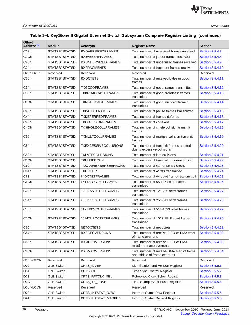
Summary of Modules www.ti.com
86 SPRUGV9D–November 2010–Revised June 2013Submit Documentation Feedback
Copyright © 2010–2013, Texas Instruments Incorporated
Registers
Table 3-4. KeyStone II Gigabit Ethernet Switch Subsystem Complete Register Listing (continued)OffsetAddress (1) Module Acronym Register Name SectionC18h STATSB/ STATSD RXOVERSIZEDFRAMES Total number of oversized frames received Section 3.5.4.7C1Ch STATSB/ STATSD RXJABBERFRAMES Total number of jabber frames received Section 3.5.4.8C20h STATSB/ STATSD RXUNDERSIZEDFRAMES Total number of undersized frames received Section 3.5.4.9C24h STATSB/ STATSD RXFRAGMENTS Total number of fragment frames received Section 3.5.4.10C28h-C2Fh Reserved Reserved Reserved ReservedC30h STATSB/ STATSD RXOCTETS Total number of received bytes in good
framesSection 3.5.4.11
C34h STATSB/ STATSD TXGOODFRAMES Total number of good frames transmitted Section 3.5.4.12C38h STATSB/ STATSD TXBROADCASTFRAMES Total number of good broadcast frames
transmittedSection 3.5.4.13
C3Ch STATSB/ STATSD TXMULTICASTFRAMES Total number of good multicast framestransmitted
Section 3.5.4.14
C40h STATSB/ STATSD TXPAUSEFRAMES Total number of pause frames transmitted Section 3.5.4.15C44h STATSB/ STATSD TXDEFERREDFRAMES Total number of frames deferred Section 3.5.4.16C48h STATSB/ STATSD TXCOLLISIONFRAMES Total number of collisions Section 3.5.4.17C4Ch STATSB/ STATSD TXSINGLECOLLFRAMES Total number of single collision transmit
framesSection 3.5.4.18
C50h STATSB/ STATSD TXMULTCOLLFRAMES Total number of multiple collision transmitframes
Section 3.5.4.19
C54h STATSB/ STATSD TXEXCESSIVECOLLISIONS Total number of transmit frames aborteddue to excessive collisions
Section 3.5.4.20
C58h STATSB/ STATSD TXLATECOLLISIONS Total number of late collisions Section 3.5.4.21C5Ch STATSB/ STATSD TXUNDERRUN Total number of transmit underrun errors Section 3.5.4.22C60h STATSB/ STATSD TXCARRIERSENSEERRORS Total number of carrier sense errors Section 3.5.4.23C64h STATSB/ STATSD TXOCTETS Total number of octets transmitted Section 3.5.4.24C68h STATSB/ STATSD 64OCTETFRAMES Total number of 64 octet frames transmitted Section 3.5.4.25C6Ch STATSB/ STATSD 65T127OCTETFRAMES Total number of 65-127 octet frames
transmittedSection 3.5.4.26
C70h STATSB/ STATSD 128T255OCTETFRAMES Total number of 128-255 octet framestransmitted
Section 3.5.4.27
C74h STATSB/ STATSD 256T511OCTETFRAMES Total number of 256-511 octet framestransmitted
Section 3.5.4.28
C78h STATSB/ STATSD 512T1023OCTETFRAMES Total number of 512-1023 octet framestransmitted
Section 3.5.4.29
C7Ch STATSB/ STATSD 1024TUPOCTETFRAMES Total number of 1023-1518 octet framestransmitted
Section 3.5.4.30
C80h STATSB/ STATSD NETOCTETS Total number of net octets Section 3.5.4.31C84h STATSB/ STATSD RXSOFOVERRUNS Total number of receive FIFO or DMA start
of frame overrunsSection 3.5.4.32
C88h STATSB/ STATSD RXMOFOVERRUNS Total number of receive FIFO or DMAmiddle of frame overruns
Section 3.5.4.33
C8Ch STATSB/ STATSD RXDMAOVERRUNS Total number of receive DMA start of frameand middle of frame overruns
Section 3.5.4.34
C90h-CFCh Reserved Reserved Reserved ReservedD00 GbE Switch CPTS_IDVER Identification and Version Register Section 3.5.5.1D04 GbE Switch CPTS_CTL Time Sync Control Register Section 3.5.5.2D08 GbE Switch CPTS_RFTCLK_SEL Reference Clock Select Register Section 3.5.5.3D0C GbE Switch CPTS_TS_PUSH Time Stamp Event Push Register Section 3.5.5.4D10h-D1Ch Reserved Reserved Reserved ReservedD20h GbE Switch CPTS_INTSTAT_RAW Interrupt Status Raw Register Section 3.5.5.5D24h GbE Switch CPTS_INTSTAT_MASKED Interrupt Status Masked Register Section 3.5.5.6
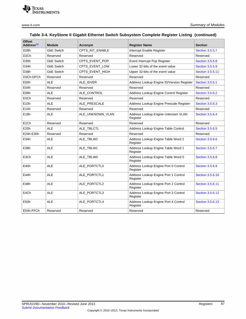
www.ti.com Summary of Modules
87SPRUGV9D–November 2010–Revised June 2013Submit Documentation Feedback
Copyright © 2010–2013, Texas Instruments Incorporated
Registers
Table 3-4. KeyStone II Gigabit Ethernet Switch Subsystem Complete Register Listing (continued)OffsetAddress (1) Module Acronym Register Name SectionD28h GbE Switch CPTS_INT_ENABLE Interrupt Enable Register Section 3.5.5.7D2Ch Reserved Reserved Reserved ReservedD30h GbE Switch CPTS_EVENT_POP Event Interrupt Pop Register Section 3.5.5.8D34h GbE Switch CPTS_EVENT_LOW Lower 32-bits of the event value Section 3.5.5.9D38h GbE Switch CPTS_EVENT_HIGH Upper 32-bits of the event value Section 3.5.5.11D3Ch-DFCh Reserved Reserved Reserved ReservedE00h ALE ALE_IDVER Address Lookup Engine ID/Version Register Section 3.5.6.1E04h Reserved Reserved Reserved ReservedE08h ALE ALE_CONTROL Address Lookup Engine Control Register Section 3.5.6.2E0Ch Reserved Reserved Reserved ReservedE10h ALE ALE_PRESCALE Address Lookup Engine Prescale Register Section 3.5.6.3E14h Reserved Reserved Reserved ReservedE18h ALE ALE_UNKNOWN_VLAN Address Lookup Engine Unknown VLAN
RegisterSection 3.5.6.4
E1Ch Reserved Reserved Reserved ReservedE20h ALE ALE_TBLCTL Address Lookup Engine Table Control Section 3.5.6.5E24h-E30h Reserved Reserved Reserved ReservedE34h ALE ALE_TBLW2 Address Lookup Engine Table Word 2
RegisterSection 3.5.6.6
E38h ALE ALE_TBLW1 Address Lookup Engine Table Word 1Register
Section 3.5.6.7
E3Ch ALE ALE_TBLW0 Address Lookup Engine Table Word 0Register
Section 3.5.6.8
E40h ALE ALE_PORTCTL0 Address Lookup Engine Port 0 ControlRegister
Section 3.5.6.9
E44h ALE ALE_PORTCTL1 Address Lookup Engine Port 1 ControlRegister
Section 3.5.6.10
E48h ALE ALE_PORTCTL2 Address Lookup Engine Port 2 ControlRegister
Section 3.5.6.11
E4Ch ALE ALE_PORTCTL3 Address Lookup Engine Port 3 ControlRegister
Section 3.5.6.12
E50h ALE ALE_PORTCTL4 Address Lookup Engine Port 4 ControlRegister
Section 3.5.6.13
E54h-FFCh Reserved Reserved Reserved Reserved
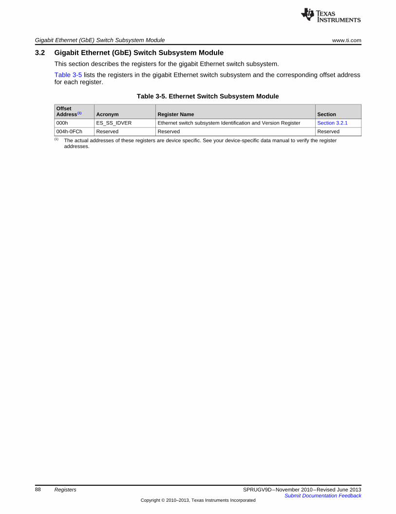
Gigabit Ethernet (GbE) Switch Subsystem Module www.ti.com
88 SPRUGV9D–November 2010–Revised June 2013Submit Documentation Feedback
Copyright © 2010–2013, Texas Instruments Incorporated
Registers
3.2 Gigabit Ethernet (GbE) Switch Subsystem ModuleThis section describes the registers for the gigabit Ethernet switch subsystem.
Table 3-5 lists the registers in the gigabit Ethernet switch subsystem and the corresponding offset addressfor each register.
(1) The actual addresses of these registers are device specific. See your device-specific data manual to verify the registeraddresses.
Table 3-5. Ethernet Switch Subsystem Module
OffsetAddress (1) Acronym Register Name Section000h ES_SS_IDVER Ethernet switch subsystem Identification and Version Register Section 3.2.1004h-0FCh Reserved Reserved Reserved
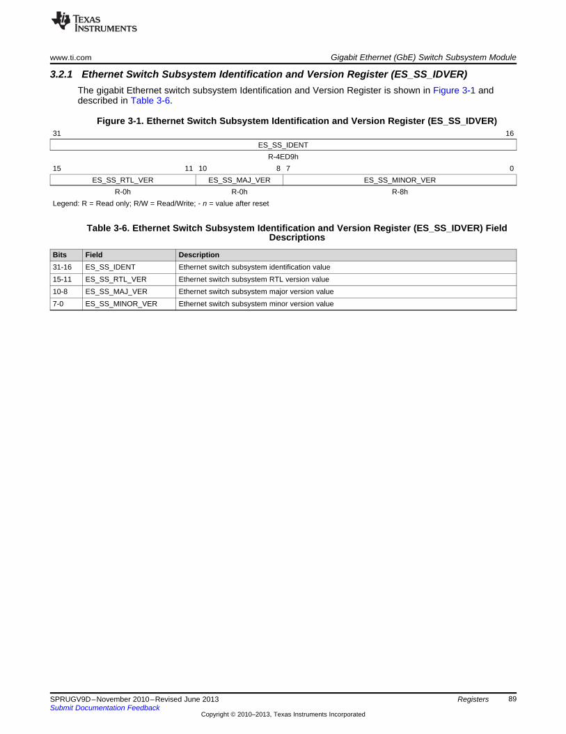
www.ti.com Gigabit Ethernet (GbE) Switch Subsystem Module
89SPRUGV9D–November 2010–Revised June 2013Submit Documentation Feedback
Copyright © 2010–2013, Texas Instruments Incorporated
Registers
3.2.1 Ethernet Switch Subsystem Identification and Version Register (ES_SS_IDVER)The gigabit Ethernet switch subsystem Identification and Version Register is shown in Figure 3-1 anddescribed in Table 3-6.
Figure 3-1. Ethernet Switch Subsystem Identification and Version Register (ES_SS_IDVER)31 16
ES_SS_IDENTR-4ED9h
15 11 10 8 7 0ES_SS_RTL_VER ES_SS_MAJ_VER ES_SS_MINOR_VER
R-0h R-0h R-8hLegend: R = Read only; R/W = Read/Write; - n = value after reset
Table 3-6. Ethernet Switch Subsystem Identification and Version Register (ES_SS_IDVER) FieldDescriptions
Bits Field Description31-16 ES_SS_IDENT Ethernet switch subsystem identification value15-11 ES_SS_RTL_VER Ethernet switch subsystem RTL version value10-8 ES_SS_MAJ_VER Ethernet switch subsystem major version value7-0 ES_SS_MINOR_VER Ethernet switch subsystem minor version value
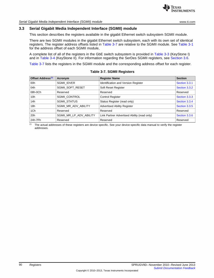
Serial Gigabit Media Independent Interface (SGMII) module www.ti.com
90 SPRUGV9D–November 2010–Revised June 2013Submit Documentation Feedback
Copyright © 2010–2013, Texas Instruments Incorporated
Registers
3.3 Serial Gigabit Media Independent Interface (SGMII) moduleThis section describes the registers available in the gigabit Ethernet switch subsystem SGMII module.
There are two SGMII modules in the gigabit Ethernet switch subsystem, each with its own set of identicalregisters. The register address offsets listed in Table 3-7 are relative to the SGMII module. See Table 3-1for the address offset of each SGMII module,
A complete list of all of the registers in the GbE switch subsystem is provided in Table 3-3 (KeyStone I)and in Table 3-4 (KeyStone II). For information regarding the SerDes SGMII registers, see Section 3.6.
Table 3-7 lists the registers in the SGMII module and the corresponding address offset for each register.
(1) The actual addresses of these registers are device specific. See your device-specific data manual to verify the registeraddresses.
Table 3-7. SGMII Registers
Offset Address (1) Acronym Register Name Section00h SGMII_IDVER Identification and Version Register Section 3.3.104h SGMII_SOFT_RESET Soft Reset Register Section 3.3.208h-0Ch Reserved Reserved Reserved10h SGMII_CONTROL Control Register Section 3.3.314h SGMII_STATUS Status Register (read only) Section 3.3.418h SGMII_MR_ADV_ABILITY Advertised Ability Register Section 3.3.51Ch Reserved Reserved Reserved20h SGMII_MR_LP_ADV_ABILITY Link Partner Advertised Ability (read only) Section 3.3.624h-7Fh Reserved Reserved Reserved
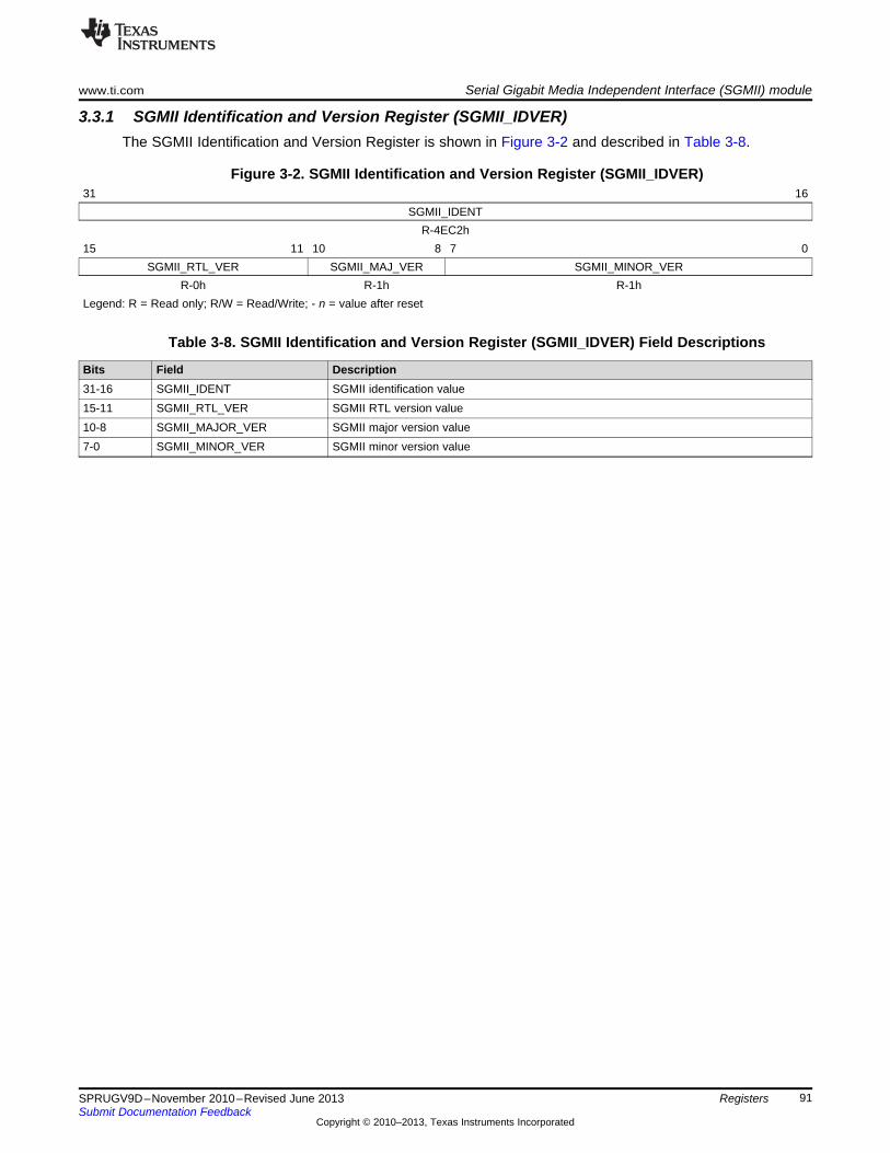
www.ti.com Serial Gigabit Media Independent Interface (SGMII) module
91SPRUGV9D–November 2010–Revised June 2013Submit Documentation Feedback
Copyright © 2010–2013, Texas Instruments Incorporated
Registers
3.3.1 SGMII Identification and Version Register (SGMII_IDVER)The SGMII Identification and Version Register is shown in Figure 3-2 and described in Table 3-8.
Figure 3-2. SGMII Identification and Version Register (SGMII_IDVER)31 16
SGMII_IDENTR-4EC2h
15 11 10 8 7 0SGMII_RTL_VER SGMII_MAJ_VER SGMII_MINOR_VER
R-0h R-1h R-1hLegend: R = Read only; R/W = Read/Write; - n = value after reset
Table 3-8. SGMII Identification and Version Register (SGMII_IDVER) Field Descriptions
Bits Field Description31-16 SGMII_IDENT SGMII identification value15-11 SGMII_RTL_VER SGMII RTL version value10-8 SGMII_MAJOR_VER SGMII major version value7-0 SGMII_MINOR_VER SGMII minor version value
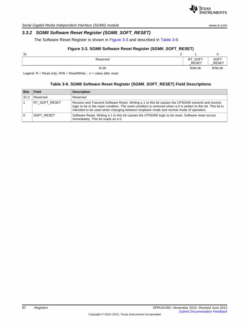
Serial Gigabit Media Independent Interface (SGMII) module www.ti.com
92 SPRUGV9D–November 2010–Revised June 2013Submit Documentation Feedback
Copyright © 2010–2013, Texas Instruments Incorporated
Registers
3.3.2 SGMII Software Reset Register (SGMII_SOFT_RESET)The Software Reset Register is shown in Figure 3-3 and described in Table 3-9.
Figure 3-3. SGMII Software Reset Register (SGMII_SOFT_RESET)31 2 1 0
Reserved RT_SOFT_RESET
SOFT_RESET
R-0h R/W-0h R/W-0hLegend: R = Read only; R/W = Read/Write; - n = value after reset
Table 3-9. SGMII Software Reset Register (SGMII_SOFT_RESET) Field Descriptions
Bits Field Description31-2 Reserved Reserved1 RT_SOFT_RESET Receive and Transmit Software Reset. Writing a 1 to this bit causes the CPSGMII transmit and receive
logic to be in the reset condition. The reset condition is removed when a 0 is written to this bit. This bit isintended to be used when changing between loopback mode and normal mode of operation.
0 SOFT_RESET Software Reset. Writing a 1 to this bit causes the CPSGMII logic to be reset. Software reset occursimmediately. This bit reads as a 0.
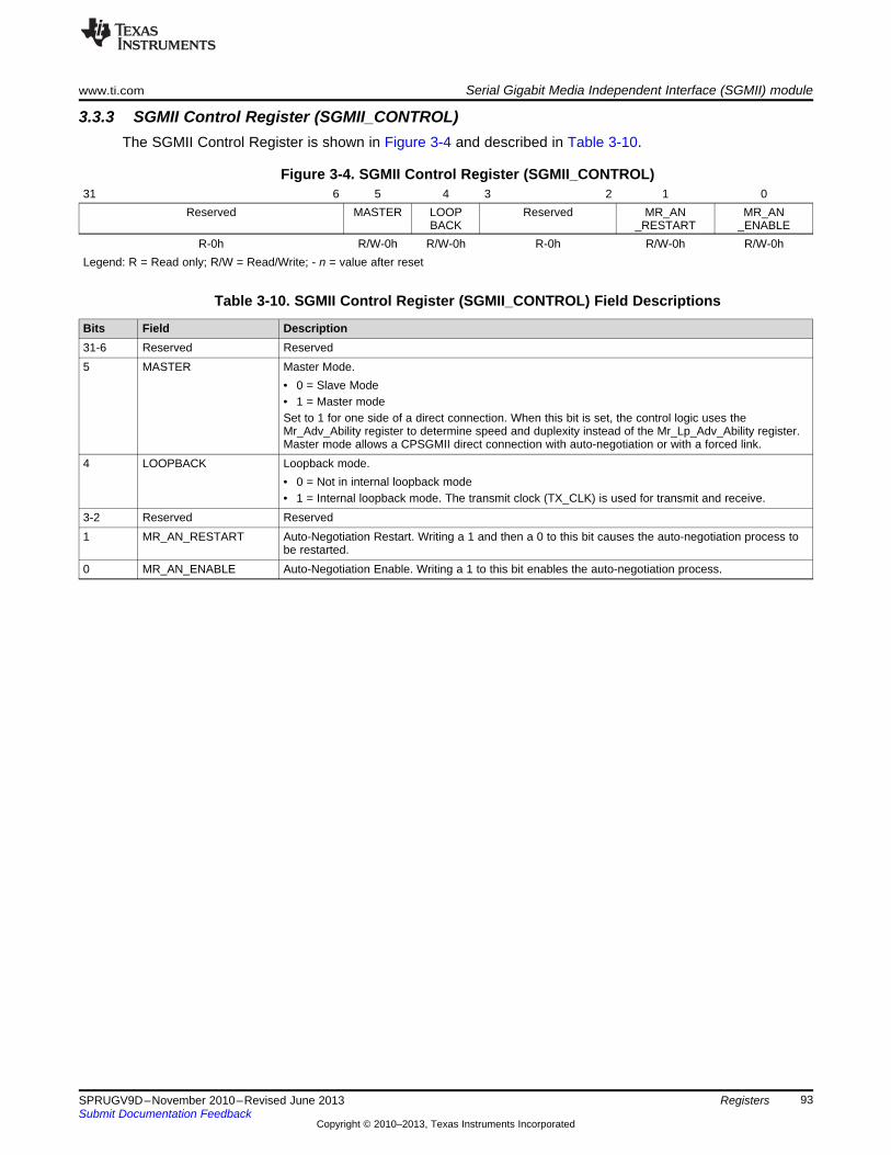
www.ti.com Serial Gigabit Media Independent Interface (SGMII) module
93SPRUGV9D–November 2010–Revised June 2013Submit Documentation Feedback
Copyright © 2010–2013, Texas Instruments Incorporated
Registers
3.3.3 SGMII Control Register (SGMII_CONTROL)The SGMII Control Register is shown in Figure 3-4 and described in Table 3-10.
Figure 3-4. SGMII Control Register (SGMII_CONTROL)31 6 5 4 3 2 1 0
Reserved MASTER LOOPBACK
Reserved MR_AN_RESTART
MR_AN_ENABLE
R-0h R/W-0h R/W-0h R-0h R/W-0h R/W-0hLegend: R = Read only; R/W = Read/Write; - n = value after reset
Table 3-10. SGMII Control Register (SGMII_CONTROL) Field Descriptions
Bits Field Description31-6 Reserved Reserved5 MASTER Master Mode.
• 0 = Slave Mode• 1 = Master modeSet to 1 for one side of a direct connection. When this bit is set, the control logic uses theMr_Adv_Ability register to determine speed and duplexity instead of the Mr_Lp_Adv_Ability register.Master mode allows a CPSGMII direct connection with auto-negotiation or with a forced link.
4 LOOPBACK Loopback mode.• 0 = Not in internal loopback mode• 1 = Internal loopback mode. The transmit clock (TX_CLK) is used for transmit and receive.
3-2 Reserved Reserved1 MR_AN_RESTART Auto-Negotiation Restart. Writing a 1 and then a 0 to this bit causes the auto-negotiation process to
be restarted.0 MR_AN_ENABLE Auto-Negotiation Enable. Writing a 1 to this bit enables the auto-negotiation process.
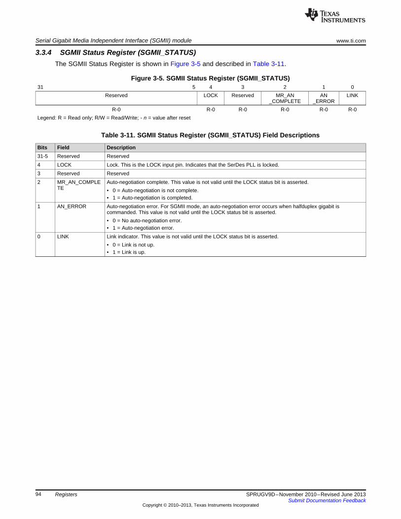
Serial Gigabit Media Independent Interface (SGMII) module www.ti.com
94 SPRUGV9D–November 2010–Revised June 2013Submit Documentation Feedback
Copyright © 2010–2013, Texas Instruments Incorporated
Registers
3.3.4 SGMII Status Register (SGMII_STATUS)The SGMII Status Register is shown in Figure 3-5 and described in Table 3-11.
Figure 3-5. SGMII Status Register (SGMII_STATUS)31 5 4 3 2 1 0
Reserved LOCK Reserved MR_AN_COMPLETE
AN_ERROR
LINK
R-0 R-0 R-0 R-0 R-0 R-0Legend: R = Read only; R/W = Read/Write; - n = value after reset
Table 3-11. SGMII Status Register (SGMII_STATUS) Field Descriptions
Bits Field Description31-5 Reserved Reserved4 LOCK Lock. This is the LOCK input pin. Indicates that the SerDes PLL is locked.3 Reserved Reserved2 MR_AN_COMPLE
TEAuto-negotiation complete. This value is not valid until the LOCK status bit is asserted.• 0 = Auto-negotiation is not complete.• 1 = Auto-negotiation is completed.
1 AN_ERROR Auto-negotiation error. For SGMII mode, an auto-negotiation error occurs when halfduplex gigabit iscommanded. This value is not valid until the LOCK status bit is asserted.• 0 = No auto-negotiation error.• 1 = Auto-negotiation error.
0 LINK Link indicator. This value is not valid until the LOCK status bit is asserted.• 0 = Link is not up.• 1 = Link is up.
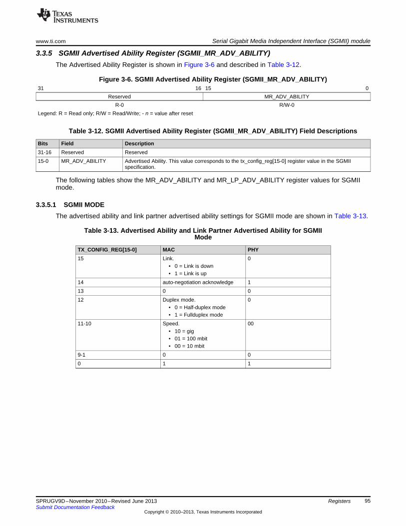
www.ti.com Serial Gigabit Media Independent Interface (SGMII) module
95SPRUGV9D–November 2010–Revised June 2013Submit Documentation Feedback
Copyright © 2010–2013, Texas Instruments Incorporated
Registers
3.3.5 SGMII Advertised Ability Register (SGMII_MR_ADV_ABILITY)The Advertised Ability Register is shown in Figure 3-6 and described in Table 3-12.
Figure 3-6. SGMII Advertised Ability Register (SGMII_MR_ADV_ABILITY)31 16 15 0
Reserved MR_ADV_ABILITYR-0 R/W-0
Legend: R = Read only; R/W = Read/Write; - n = value after reset
Table 3-12. SGMII Advertised Ability Register (SGMII_MR_ADV_ABILITY) Field Descriptions
Bits Field Description31-16 Reserved Reserved15-0 MR_ADV_ABILITY Advertised Ability. This value corresponds to the tx_config_reg[15-0] register value in the SGMII
specification.
The following tables show the MR_ADV_ABILITY and MR_LP_ADV_ABILITY register values for SGMIImode.
3.3.5.1 SGMII MODEThe advertised ability and link partner advertised ability settings for SGMII mode are shown in Table 3-13.
Table 3-13. Advertised Ability and Link Partner Advertised Ability for SGMIIMode
TX_CONFIG_REG[15-0] MAC PHY15 Link.
• 0 = Link is down• 1 = Link is up
0
14 auto-negotiation acknowledge 113 0 012 Duplex mode.
• 0 = Half-duplex mode• 1 = Fullduplex mode
0
11-10 Speed.• 10 = gig• 01 = 100 mbit• 00 = 10 mbit
00
9-1 0 00 1 1
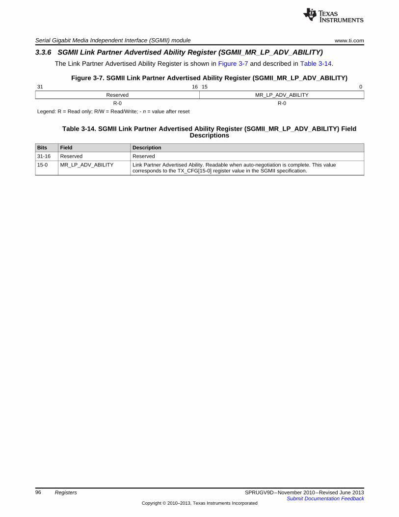
Serial Gigabit Media Independent Interface (SGMII) module www.ti.com
96 SPRUGV9D–November 2010–Revised June 2013Submit Documentation Feedback
Copyright © 2010–2013, Texas Instruments Incorporated
Registers
3.3.6 SGMII Link Partner Advertised Ability Register (SGMII_MR_LP_ADV_ABILITY)The Link Partner Advertised Ability Register is shown in Figure 3-7 and described in Table 3-14.
Figure 3-7. SGMII Link Partner Advertised Ability Register (SGMII_MR_LP_ADV_ABILITY)31 16 15 0
Reserved MR_LP_ADV_ABILITYR-0 R-0
Legend: R = Read only; R/W = Read/Write; - n = value after reset
Table 3-14. SGMII Link Partner Advertised Ability Register (SGMII_MR_LP_ADV_ABILITY) FieldDescriptions
Bits Field Description31-16 Reserved Reserved15-0 MR_LP_ADV_ABILITY Link Partner Advertised Ability. Readable when auto-negotiation is complete. This value
corresponds to the TX_CFG[15-0] register value in the SGMII specification.
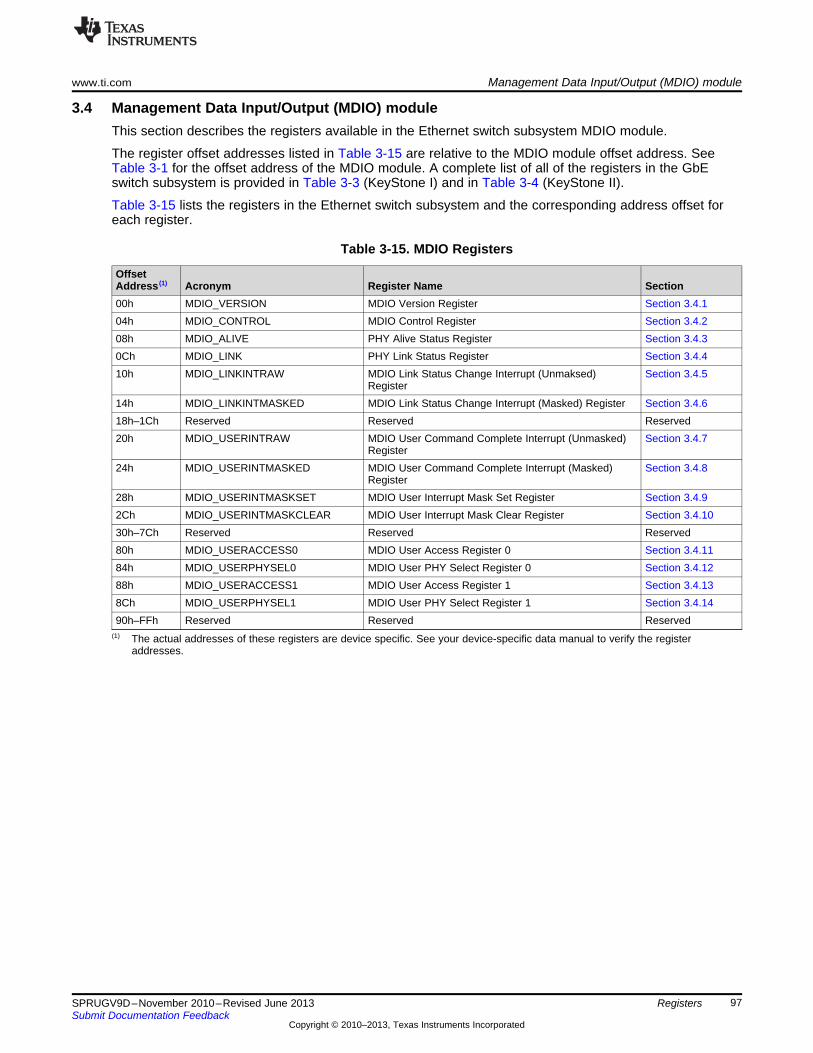
www.ti.com Management Data Input/Output (MDIO) module
97SPRUGV9D–November 2010–Revised June 2013Submit Documentation Feedback
Copyright © 2010–2013, Texas Instruments Incorporated
Registers
3.4 Management Data Input/Output (MDIO) moduleThis section describes the registers available in the Ethernet switch subsystem MDIO module.
The register offset addresses listed in Table 3-15 are relative to the MDIO module offset address. SeeTable 3-1 for the offset address of the MDIO module. A complete list of all of the registers in the GbEswitch subsystem is provided in Table 3-3 (KeyStone I) and in Table 3-4 (KeyStone II).
Table 3-15 lists the registers in the Ethernet switch subsystem and the corresponding address offset foreach register.
(1) The actual addresses of these registers are device specific. See your device-specific data manual to verify the registeraddresses.
Table 3-15. MDIO Registers
OffsetAddress (1) Acronym Register Name Section00h MDIO_VERSION MDIO Version Register Section 3.4.104h MDIO_CONTROL MDIO Control Register Section 3.4.208h MDIO_ALIVE PHY Alive Status Register Section 3.4.30Ch MDIO_LINK PHY Link Status Register Section 3.4.410h MDIO_LINKINTRAW MDIO Link Status Change Interrupt (Unmaksed)
RegisterSection 3.4.5
14h MDIO_LINKINTMASKED MDIO Link Status Change Interrupt (Masked) Register Section 3.4.618h–1Ch Reserved Reserved Reserved20h MDIO_USERINTRAW MDIO User Command Complete Interrupt (Unmasked)
RegisterSection 3.4.7
24h MDIO_USERINTMASKED MDIO User Command Complete Interrupt (Masked)Register
Section 3.4.8
28h MDIO_USERINTMASKSET MDIO User Interrupt Mask Set Register Section 3.4.92Ch MDIO_USERINTMASKCLEAR MDIO User Interrupt Mask Clear Register Section 3.4.1030h–7Ch Reserved Reserved Reserved80h MDIO_USERACCESS0 MDIO User Access Register 0 Section 3.4.1184h MDIO_USERPHYSEL0 MDIO User PHY Select Register 0 Section 3.4.1288h MDIO_USERACCESS1 MDIO User Access Register 1 Section 3.4.138Ch MDIO_USERPHYSEL1 MDIO User PHY Select Register 1 Section 3.4.1490h–FFh Reserved Reserved Reserved
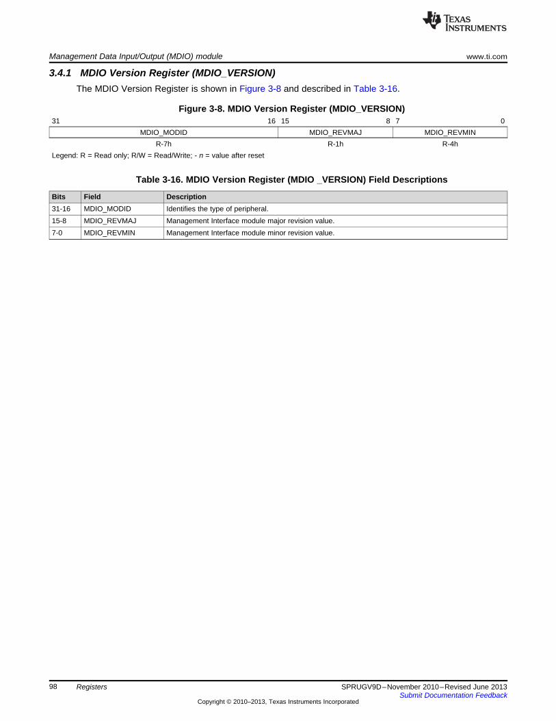
Management Data Input/Output (MDIO) module www.ti.com
98 SPRUGV9D–November 2010–Revised June 2013Submit Documentation Feedback
Copyright © 2010–2013, Texas Instruments Incorporated
Registers
3.4.1 MDIO Version Register (MDIO_VERSION)The MDIO Version Register is shown in Figure 3-8 and described in Table 3-16.
Figure 3-8. MDIO Version Register (MDIO_VERSION)31 16 15 8 7 0
MDIO_MODID MDIO_REVMAJ MDIO_REVMINR-7h R-1h R-4h
Legend: R = Read only; R/W = Read/Write; - n = value after reset
Table 3-16. MDIO Version Register (MDIO _VERSION) Field Descriptions
Bits Field Description31-16 MDIO_MODID Identifies the type of peripheral.15-8 MDIO_REVMAJ Management Interface module major revision value.7-0 MDIO_REVMIN Management Interface module minor revision value.
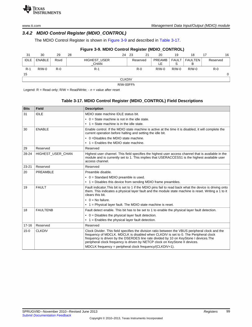
www.ti.com Management Data Input/Output (MDIO) module
99SPRUGV9D–November 2010–Revised June 2013Submit Documentation Feedback
Copyright © 2010–2013, Texas Instruments Incorporated
Registers
3.4.2 MDIO Control Register (MDIO_CONTROL)The MDIO Control Register is shown in Figure 3-9 and described in Table 3-17.
Figure 3-9. MDIO Control Register (MDIO_CONTROL)31 30 29 28 24 23 21 20 19 18 17 16
IDLE ENABLE Rsvd HIGHEST_USER_CHAN
Reserved PREAMBLE
FAULTS
FAULTENB
Reserved
R-1 R/W-0 R-0 R-1 R-0 R/W-0 R/W-0 R/W-0 R-015 0
CLKDIVR/W-00FFh
Legend: R = Read only; R/W = Read/Write; - n = value after reset
Table 3-17. MDIO Control Register (MDIO_CONTROL) Field Descriptions
Bits Field Description31 IDLE MDIO state machine IDLE status bit.
• 0 = State machine is not in the idle state.• 1 = State machine is in the idle state.
30 ENABLE Enable control. If the MDIO state machine is active at the time it is disabled, it will complete thecurrent operation before halting and setting the idle bit.• 0 =Disables the MDIO state machine.• 1 = Enables the MDIO state machine.
29 Reserved Reserved28-24 HIGHEST_USER_CHAN Highest user channel. This field specifies the highest user access channel that is available in the
module and is currently set to 1. This implies that USERACCESS1 is the highest available useraccess channel.
23-21 Reserved Reserved20 PREAMBLE Preamble disable.
• 0 = Standard MDIO preamble is used.• 1 = Disables this device from sending MDIO frame preambles.
19 FAULT Fault indicator.This bit is set to 1 if the MDIO pins fail to read back what the device is driving ontothem. This indicates a physical layer fault and the module state machine is reset. Writing a 1 to itclears this bit.• 0 = No failure.• 1 = Physical layer fault. The MDIO state machine is reset.
18 FAULTENB Fault detect enable. This bit has to be set to 1 to enable the physical layer fault detection.• 0 = Disables the physical layer fault detection.• 1 = Enables the physical layer fault detection.
17-16 Reserved Reserved15-0 CLKDIV Clock Divider. This field specifies the division ratio between the VBUS peripheral clock and the
frequency of MDCLK. MDCLK is disabled when CLKDIV is set to 0. The Peripheral clockfrequency is driven by the DSERDES line rate divided by 10 on KeyStone I devices.Theperipheral clock frequency is driven by NETCP clock on KeyStone II devices.MDCLK frequency = peripheral clock frequency/(CLKDIV+1).
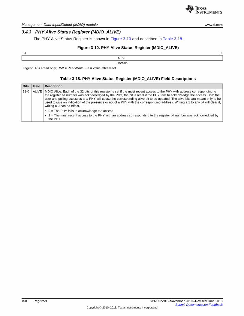
Management Data Input/Output (MDIO) module www.ti.com
100 SPRUGV9D–November 2010–Revised June 2013Submit Documentation Feedback
Copyright © 2010–2013, Texas Instruments Incorporated
Registers
3.4.3 PHY Alive Status Register (MDIO_ALIVE)The PHY Alive Status Register is shown in Figure 3-10 and described in Table 3-18.
Figure 3-10. PHY Alive Status Register (MDIO_ALIVE)31 0
ALIVER/W-0h
Legend: R = Read only; R/W = Read/Write; - n = value after reset
Table 3-18. PHY Alive Status Register (MDIO_ALIVE) Field Descriptions
Bits Field Description31-0 ALIVE MDIO Alive. Each of the 32 bits of this register is set if the most recent access to the PHY with address corresponding to
the register bit number was acknowledged by the PHY, the bit is reset if the PHY fails to acknowledge the access. Both theuser and polling accesses to a PHY will cause the corresponding alive bit to be updated. The alive bits are meant only to beused to give an indication of the presence or not of a PHY with the corresponding address. Writing a 1 to any bit will clear it,writing a 0 has no effect.• 0 = The PHY fails to acknowledge the access• 1 = The most recent access to the PHY with an address corresponding to the register bit number was acknowledged by
the PHY
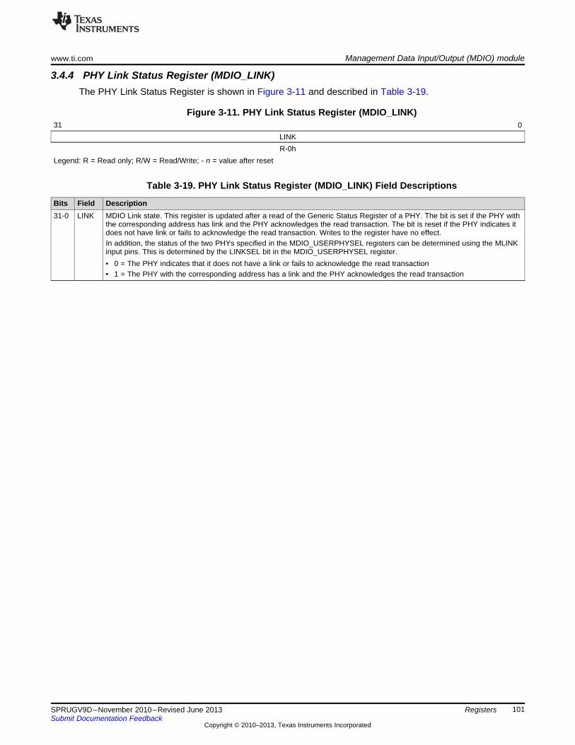
www.ti.com Management Data Input/Output (MDIO) module
101SPRUGV9D–November 2010–Revised June 2013Submit Documentation Feedback
Copyright © 2010–2013, Texas Instruments Incorporated
Registers
3.4.4 PHY Link Status Register (MDIO_LINK)The PHY Link Status Register is shown in Figure 3-11 and described in Table 3-19.
Figure 3-11. PHY Link Status Register (MDIO_LINK)31 0
LINKR-0h
Legend: R = Read only; R/W = Read/Write; - n = value after reset
Table 3-19. PHY Link Status Register (MDIO_LINK) Field Descriptions
Bits Field Description31-0 LINK MDIO Link state. This register is updated after a read of the Generic Status Register of a PHY. The bit is set if the PHY with
the corresponding address has link and the PHY acknowledges the read transaction. The bit is reset if the PHY indicates itdoes not have link or fails to acknowledge the read transaction. Writes to the register have no effect.In addition, the status of the two PHYs specified in the MDIO_USERPHYSEL registers can be determined using the MLINKinput pins. This is determined by the LINKSEL bit in the MDIO_USERPHYSEL register.• 0 = The PHY indicates that it does not have a link or fails to acknowledge the read transaction• 1 = The PHY with the corresponding address has a link and the PHY acknowledges the read transaction
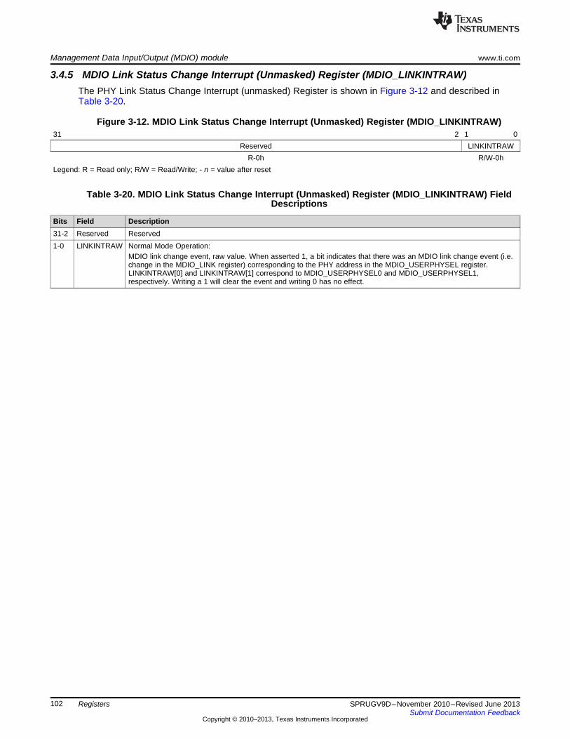
Management Data Input/Output (MDIO) module www.ti.com
102 SPRUGV9D–November 2010–Revised June 2013Submit Documentation Feedback
Copyright © 2010–2013, Texas Instruments Incorporated
Registers
3.4.5 MDIO Link Status Change Interrupt (Unmasked) Register (MDIO_LINKINTRAW)The PHY Link Status Change Interrupt (unmasked) Register is shown in Figure 3-12 and described inTable 3-20.
Figure 3-12. MDIO Link Status Change Interrupt (Unmasked) Register (MDIO_LINKINTRAW)31 2 1 0
Reserved LINKINTRAWR-0h R/W-0h
Legend: R = Read only; R/W = Read/Write; - n = value after reset
Table 3-20. MDIO Link Status Change Interrupt (Unmasked) Register (MDIO_LINKINTRAW) FieldDescriptions
Bits Field Description31-2 Reserved Reserved1-0 LINKINTRAW Normal Mode Operation:
MDIO link change event, raw value. When asserted 1, a bit indicates that there was an MDIO link change event (i.e.change in the MDIO_LINK register) corresponding to the PHY address in the MDIO_USERPHYSEL register.LINKINTRAW[0] and LINKINTRAW[1] correspond to MDIO_USERPHYSEL0 and MDIO_USERPHYSEL1,respectively. Writing a 1 will clear the event and writing 0 has no effect.
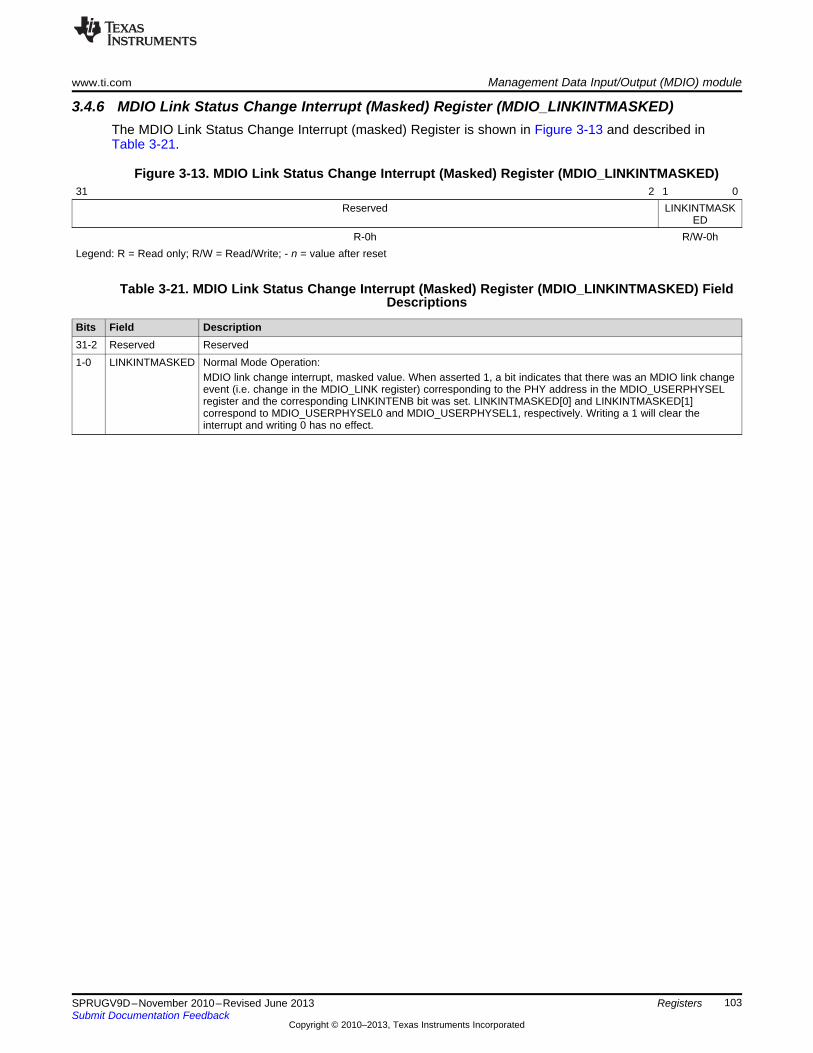
www.ti.com Management Data Input/Output (MDIO) module
103SPRUGV9D–November 2010–Revised June 2013Submit Documentation Feedback
Copyright © 2010–2013, Texas Instruments Incorporated
Registers
3.4.6 MDIO Link Status Change Interrupt (Masked) Register (MDIO_LINKINTMASKED)The MDIO Link Status Change Interrupt (masked) Register is shown in Figure 3-13 and described inTable 3-21.
Figure 3-13. MDIO Link Status Change Interrupt (Masked) Register (MDIO_LINKINTMASKED)31 2 1 0
Reserved LINKINTMASKED
R-0h R/W-0hLegend: R = Read only; R/W = Read/Write; - n = value after reset
Table 3-21. MDIO Link Status Change Interrupt (Masked) Register (MDIO_LINKINTMASKED) FieldDescriptions
Bits Field Description31-2 Reserved Reserved1-0 LINKINTMASKED Normal Mode Operation:
MDIO link change interrupt, masked value. When asserted 1, a bit indicates that there was an MDIO link changeevent (i.e. change in the MDIO_LINK register) corresponding to the PHY address in the MDIO_USERPHYSELregister and the corresponding LINKINTENB bit was set. LINKINTMASKED[0] and LINKINTMASKED[1]correspond to MDIO_USERPHYSEL0 and MDIO_USERPHYSEL1, respectively. Writing a 1 will clear theinterrupt and writing 0 has no effect.
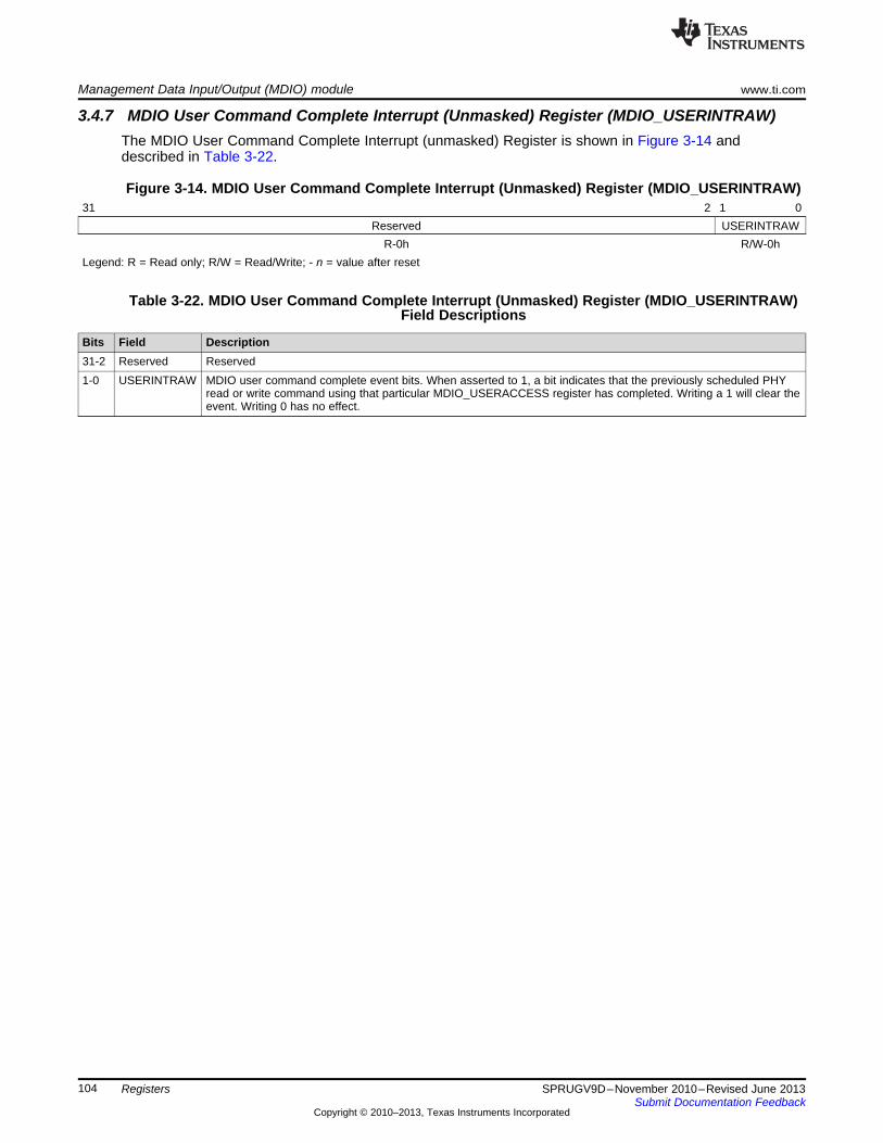
Management Data Input/Output (MDIO) module www.ti.com
104 SPRUGV9D–November 2010–Revised June 2013Submit Documentation Feedback
Copyright © 2010–2013, Texas Instruments Incorporated
Registers
3.4.7 MDIO User Command Complete Interrupt (Unmasked) Register (MDIO_USERINTRAW)The MDIO User Command Complete Interrupt (unmasked) Register is shown in Figure 3-14 anddescribed in Table 3-22.
Figure 3-14. MDIO User Command Complete Interrupt (Unmasked) Register (MDIO_USERINTRAW)31 2 1 0
Reserved USERINTRAWR-0h R/W-0h
Legend: R = Read only; R/W = Read/Write; - n = value after reset
Table 3-22. MDIO User Command Complete Interrupt (Unmasked) Register (MDIO_USERINTRAW)Field Descriptions
Bits Field Description31-2 Reserved Reserved1-0 USERINTRAW MDIO user command complete event bits. When asserted to 1, a bit indicates that the previously scheduled PHY
read or write command using that particular MDIO_USERACCESS register has completed. Writing a 1 will clear theevent. Writing 0 has no effect.
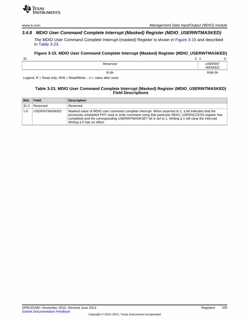
www.ti.com Management Data Input/Output (MDIO) module
105SPRUGV9D–November 2010–Revised June 2013Submit Documentation Feedback
Copyright © 2010–2013, Texas Instruments Incorporated
Registers
3.4.8 MDIO User Command Complete Interrupt (Masked) Register (MDIO_USERINTMASKED)The MDIO User Command Complete Interrupt (masked) Register is shown in Figure 3-15 and describedin Table 3-23.
Figure 3-15. MDIO User Command Complete Interrupt (Masked) Register (MDIO_USERINTMASKED)31 2 1 0
Reserved USERINTMASKED
R-0h R/W-0hLegend: R = Read only; R/W = Read/Write; - n = value after reset
Table 3-23. MDIO User Command Complete Interrupt (Masked) Register (MDIO_USERINTMASKED)Field Descriptions
Bits Field Description31-2 Reserved Reserved1-0 USERINTMASKED Masked value of MDIO user command complete interrupt. When asserted to 1, a bit indicates that the
previously scheduled PHY read or write command using that particular MDIO_USERACCESS register hascompleted and the corresponding USERINTMASKSET bit is set to 1. Writing a 1 will clear the interrupt.Writing a 0 has no effect.
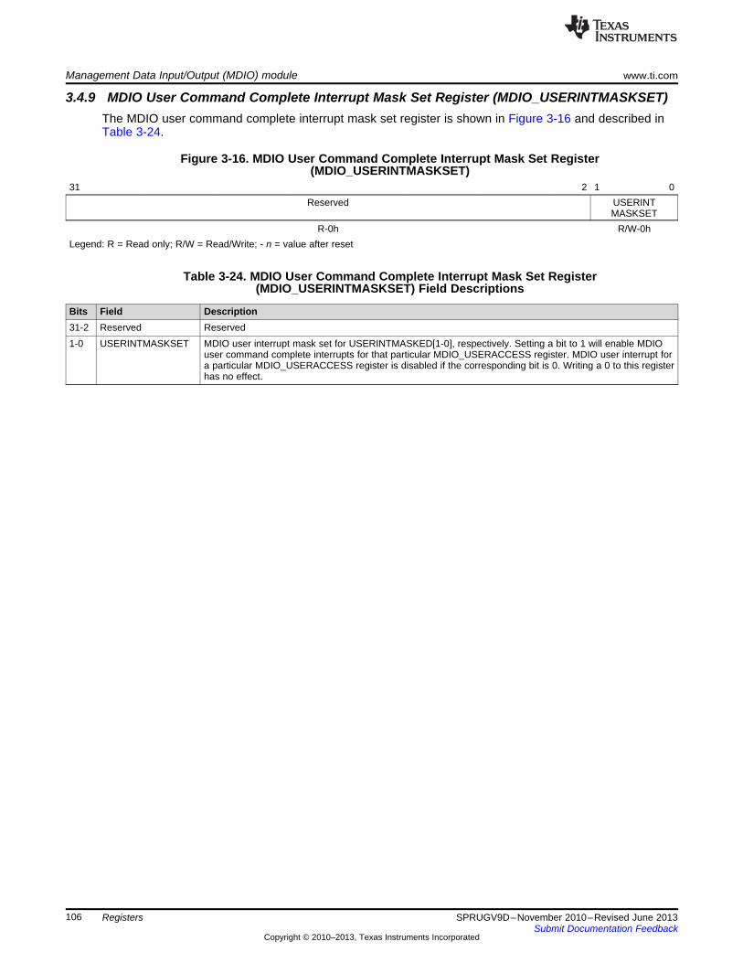
Management Data Input/Output (MDIO) module www.ti.com
106 SPRUGV9D–November 2010–Revised June 2013Submit Documentation Feedback
Copyright © 2010–2013, Texas Instruments Incorporated
Registers
3.4.9 MDIO User Command Complete Interrupt Mask Set Register (MDIO_USERINTMASKSET)The MDIO user command complete interrupt mask set register is shown in Figure 3-16 and described inTable 3-24.
Figure 3-16. MDIO User Command Complete Interrupt Mask Set Register(MDIO_USERINTMASKSET)
31 2 1 0Reserved USERINT
MASKSETR-0h R/W-0h
Legend: R = Read only; R/W = Read/Write; - n = value after reset
Table 3-24. MDIO User Command Complete Interrupt Mask Set Register(MDIO_USERINTMASKSET) Field Descriptions
Bits Field Description31-2 Reserved Reserved1-0 USERINTMASKSET MDIO user interrupt mask set for USERINTMASKED[1-0], respectively. Setting a bit to 1 will enable MDIO
user command complete interrupts for that particular MDIO_USERACCESS register. MDIO user interrupt fora particular MDIO_USERACCESS register is disabled if the corresponding bit is 0. Writing a 0 to this registerhas no effect.
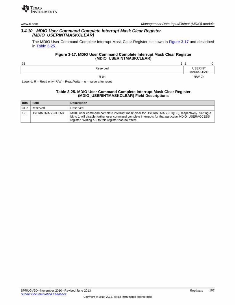
www.ti.com Management Data Input/Output (MDIO) module
107SPRUGV9D–November 2010–Revised June 2013Submit Documentation Feedback
Copyright © 2010–2013, Texas Instruments Incorporated
Registers
3.4.10 MDIO User Command Complete Interrupt Mask Clear Register(MDIO_USERINTMASKCLEAR)The MDIO User Command Complete Interrupt Mask Clear Register is shown in Figure 3-17 and describedin Table 3-25.
Figure 3-17. MDIO User Command Complete Interrupt Mask Clear Register(MDIO_USERINTMASKCLEAR)
31 2 1 0Reserved USERINT
MASKCLEARR-0h R/W-0h
Legend: R = Read only; R/W = Read/Write; - n = value after reset
Table 3-25. MDIO User Command Complete Interrupt Mask Clear Register(MDIO_USERINTMASKCLEAR) Field Descriptions
Bits Field Description31-2 Reserved Reserved1-0 USERINTMASKCLEAR MDIO user command complete interrupt mask clear for USERINTMASKED[1-0], respectively. Setting a
bit to 1 will disable further user command complete interrupts for that particular MDIO_USERACCESSregister. Writing a 0 to this register has no effect.
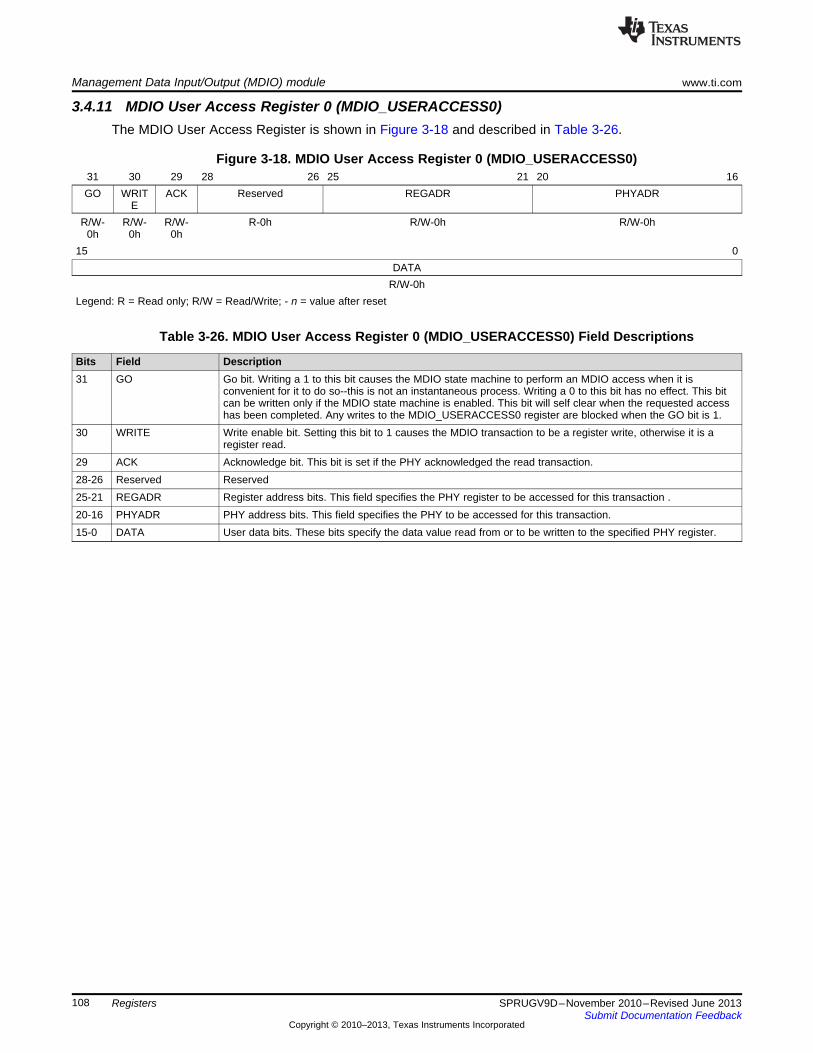
Management Data Input/Output (MDIO) module www.ti.com
108 SPRUGV9D–November 2010–Revised June 2013Submit Documentation Feedback
Copyright © 2010–2013, Texas Instruments Incorporated
Registers
3.4.11 MDIO User Access Register 0 (MDIO_USERACCESS0)The MDIO User Access Register is shown in Figure 3-18 and described in Table 3-26.
Figure 3-18. MDIO User Access Register 0 (MDIO_USERACCESS0)31 30 29 28 26 25 21 20 16GO WRIT
EACK Reserved REGADR PHYADR
R/W-0h
R/W-0h
R/W-0h
R-0h R/W-0h R/W-0h
15 0DATA
R/W-0hLegend: R = Read only; R/W = Read/Write; - n = value after reset
Table 3-26. MDIO User Access Register 0 (MDIO_USERACCESS0) Field Descriptions
Bits Field Description31 GO Go bit. Writing a 1 to this bit causes the MDIO state machine to perform an MDIO access when it is
convenient for it to do so--this is not an instantaneous process. Writing a 0 to this bit has no effect. This bitcan be written only if the MDIO state machine is enabled. This bit will self clear when the requested accesshas been completed. Any writes to the MDIO_USERACCESS0 register are blocked when the GO bit is 1.
30 WRITE Write enable bit. Setting this bit to 1 causes the MDIO transaction to be a register write, otherwise it is aregister read.
29 ACK Acknowledge bit. This bit is set if the PHY acknowledged the read transaction.28-26 Reserved Reserved25-21 REGADR Register address bits. This field specifies the PHY register to be accessed for this transaction .20-16 PHYADR PHY address bits. This field specifies the PHY to be accessed for this transaction.15-0 DATA User data bits. These bits specify the data value read from or to be written to the specified PHY register.
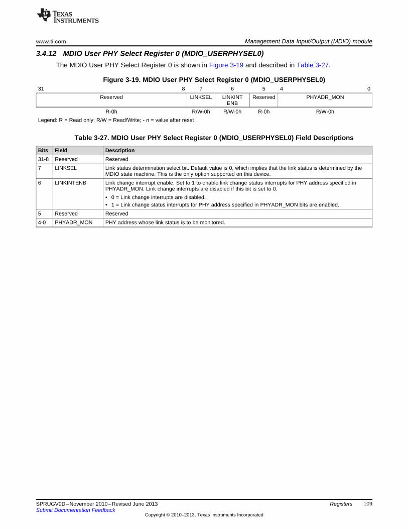
www.ti.com Management Data Input/Output (MDIO) module
109SPRUGV9D–November 2010–Revised June 2013Submit Documentation Feedback
Copyright © 2010–2013, Texas Instruments Incorporated
Registers
3.4.12 MDIO User PHY Select Register 0 (MDIO_USERPHYSEL0)The MDIO User PHY Select Register 0 is shown in Figure 3-19 and described in Table 3-27.
Figure 3-19. MDIO User PHY Select Register 0 (MDIO_USERPHYSEL0)31 8 7 6 5 4 0
Reserved LINKSEL LINKINTENB
Reserved PHYADR_MON
R-0h R/W-0h R/W-0h R-0h R/W-0hLegend: R = Read only; R/W = Read/Write; - n = value after reset
Table 3-27. MDIO User PHY Select Register 0 (MDIO_USERPHYSEL0) Field Descriptions
Bits Field Description31-8 Reserved Reserved7 LINKSEL Link status determination select bit. Default value is 0, which implies that the link status is determined by the
MDIO state machine. This is the only option supported on this device.6 LINKINTENB Link change interrupt enable. Set to 1 to enable link change status interrupts for PHY address specified in
PHYADR_MON. Link change interrupts are disabled if this bit is set to 0.• 0 = Link change interrupts are disabled.• 1 = Link change status interrupts for PHY address specified in PHYADR_MON bits are enabled.
5 Reserved Reserved4-0 PHYADR_MON PHY address whose link status is to be monitored.
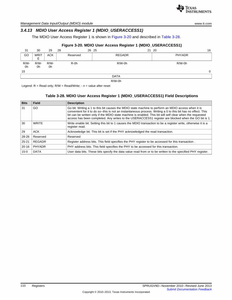
Management Data Input/Output (MDIO) module www.ti.com
110 SPRUGV9D–November 2010–Revised June 2013Submit Documentation Feedback
Copyright © 2010–2013, Texas Instruments Incorporated
Registers
3.4.13 MDIO User Access Register 1 (MDIO_USERACCESS1)The MDIO User Access Register 1 is shown in Figure 3-20 and described in Table 3-28.
Figure 3-20. MDIO User Access Register 1 (MDIO_USERACCESS1)31 30 29 28 26 25 21 20 16GO WRIT
EACK Reserved REGADR PHYADR
R/W-0h
R/W-0h
R/W-0h
R-0h R/W-0h R/W-0h
15 0DATA
R/W-0hLegend: R = Read only; R/W = Read/Write; - n = value after reset
Table 3-28. MDIO User Access Register 1 (MDIO_USERACCESS1) Field Descriptions
Bits Field Description31 GO Go bit. Writing a 1 to this bit causes the MDIO state machine to perform an MDIO access when it is
convenient for it to do so--this is not an instantaneous process. Writing a 0 to this bit has no effect. Thisbit can be written only if the MDIO state machine is enabled. This bit will self clear when the requestedaccess has been completed. Any writes to the USERACCESS1 register are blocked when the GO bit is 1.
30 WRITE Write enable bit. Setting this bit to 1 causes the MDIO transaction to be a register write, otherwise it is aregister read.
29 ACK Acknowledge bit. This bit is set if the PHY acknowledged the read transaction.28-26 Reserved Reserved25-21 REGADR Register address bits. This field specifies the PHY register to be accessed for this transaction .20-16 PHYADR PHY address bits. This field specifies the PHY to be accessed for this transaction.15-0 DATA User data bits. These bits specify the data value read from or to be written to the specified PHY register.
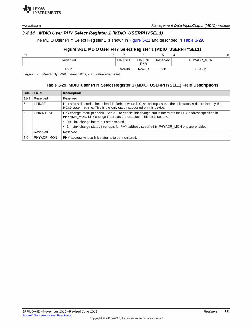
www.ti.com Management Data Input/Output (MDIO) module
111SPRUGV9D–November 2010–Revised June 2013Submit Documentation Feedback
Copyright © 2010–2013, Texas Instruments Incorporated
Registers
3.4.14 MDIO User PHY Select Register 1 (MDIO_USERPHYSEL1)The MDIO User PHY Select Register 1 is shown in Figure 3-21 and described in Table 3-29.
Figure 3-21. MDIO User PHY Select Register 1 (MDIO_USERPHYSEL1)31 8 7 6 5 4 0
Reserved LINKSEL LINKINTENB
Reserved PHYADR_MON
R-0h R/W-0h R/W-0h R-0h R/W-0hLegend: R = Read only; R/W = Read/Write; - n = value after reset
Table 3-29. MDIO User PHY Select Register 1 (MDIO_USERPHYSEL1) Field Descriptions
Bits Field Description31-8 Reserved Reserved7 LINKSEL Link status determination select bit. Default value is 0, which implies that the link status is determined by the
MDIO state machine. This is the only option supported on this device.6 LINKINTENB Link change interrupt enable. Set to 1 to enable link change status interrupts for PHY address specified in
PHYADR_MON. Link change interrupts are disabled if this bit is set to 0.• 0 = Link change interrupts are disabled.• 1 = Link change status interrupts for PHY address specified in PHYADR_MON bits are enabled.
5 Reserved Reserved4-0 PHYADR_MON PHY address whose link status is to be monitored.
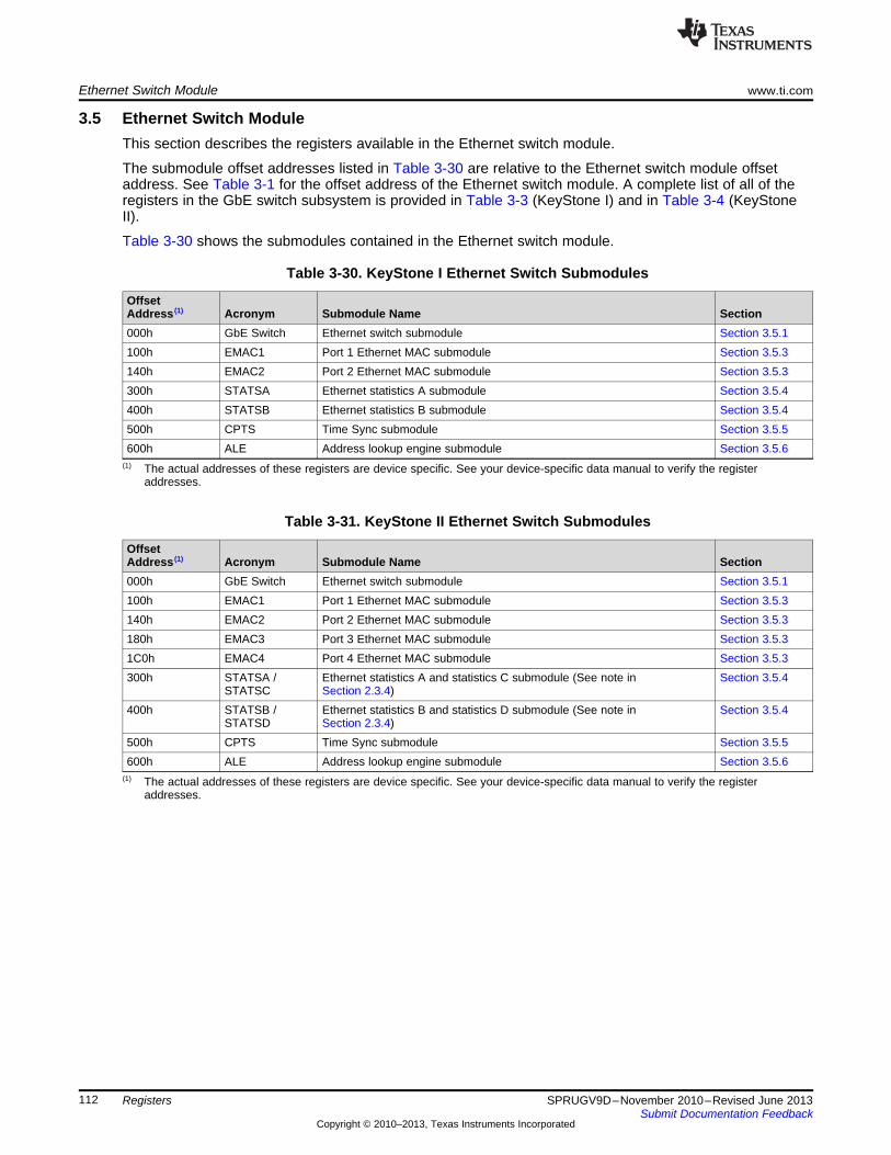
Ethernet Switch Module www.ti.com
112 SPRUGV9D–November 2010–Revised June 2013Submit Documentation Feedback
Copyright © 2010–2013, Texas Instruments Incorporated
Registers
3.5 Ethernet Switch ModuleThis section describes the registers available in the Ethernet switch module.
The submodule offset addresses listed in Table 3-30 are relative to the Ethernet switch module offsetaddress. See Table 3-1 for the offset address of the Ethernet switch module. A complete list of all of theregisters in the GbE switch subsystem is provided in Table 3-3 (KeyStone I) and in Table 3-4 (KeyStoneII).
Table 3-30 shows the submodules contained in the Ethernet switch module.
(1) The actual addresses of these registers are device specific. See your device-specific data manual to verify the registeraddresses.
Table 3-30. KeyStone I Ethernet Switch Submodules
OffsetAddress (1) Acronym Submodule Name Section000h GbE Switch Ethernet switch submodule Section 3.5.1100h EMAC1 Port 1 Ethernet MAC submodule Section 3.5.3140h EMAC2 Port 2 Ethernet MAC submodule Section 3.5.3300h STATSA Ethernet statistics A submodule Section 3.5.4400h STATSB Ethernet statistics B submodule Section 3.5.4500h CPTS Time Sync submodule Section 3.5.5600h ALE Address lookup engine submodule Section 3.5.6
(1) The actual addresses of these registers are device specific. See your device-specific data manual to verify the registeraddresses.
Table 3-31. KeyStone II Ethernet Switch Submodules
OffsetAddress (1) Acronym Submodule Name Section000h GbE Switch Ethernet switch submodule Section 3.5.1100h EMAC1 Port 1 Ethernet MAC submodule Section 3.5.3140h EMAC2 Port 2 Ethernet MAC submodule Section 3.5.3180h EMAC3 Port 3 Ethernet MAC submodule Section 3.5.31C0h EMAC4 Port 4 Ethernet MAC submodule Section 3.5.3300h STATSA /
STATSCEthernet statistics A and statistics C submodule (See note inSection 2.3.4)
Section 3.5.4
400h STATSB /STATSD
Ethernet statistics B and statistics D submodule (See note inSection 2.3.4)
Section 3.5.4
500h CPTS Time Sync submodule Section 3.5.5600h ALE Address lookup engine submodule Section 3.5.6
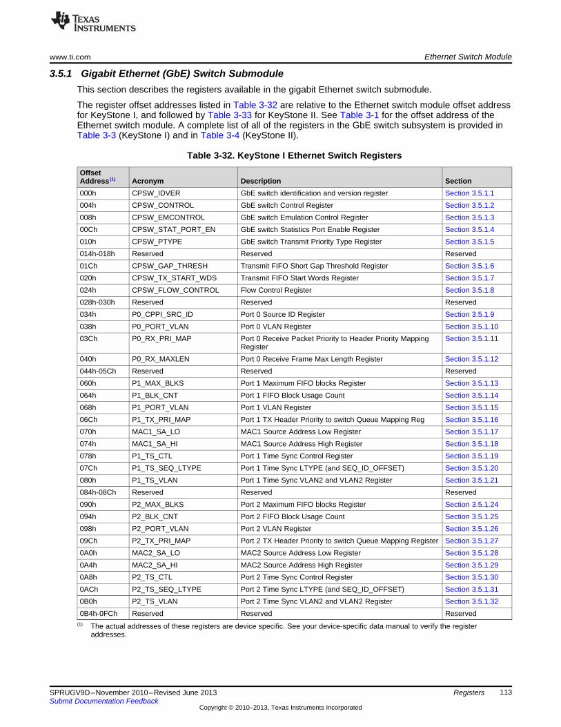
www.ti.com Ethernet Switch Module
113SPRUGV9D–November 2010–Revised June 2013Submit Documentation Feedback
Copyright © 2010–2013, Texas Instruments Incorporated
Registers
3.5.1 Gigabit Ethernet (GbE) Switch SubmoduleThis section describes the registers available in the gigabit Ethernet switch submodule.
The register offset addresses listed in Table 3-32 are relative to the Ethernet switch module offset addressfor KeyStone I, and followed by Table 3-33 for KeyStone II. See Table 3-1 for the offset address of theEthernet switch module. A complete list of all of the registers in the GbE switch subsystem is provided inTable 3-3 (KeyStone I) and in Table 3-4 (KeyStone II).
(1) The actual addresses of these registers are device specific. See your device-specific data manual to verify the registeraddresses.
Table 3-32. KeyStone I Ethernet Switch Registers
OffsetAddress (1) Acronym Description Section000h CPSW_IDVER GbE switch identification and version register Section 3.5.1.1004h CPSW_CONTROL GbE switch Control Register Section 3.5.1.2008h CPSW_EMCONTROL GbE switch Emulation Control Register Section 3.5.1.300Ch CPSW_STAT_PORT_EN GbE switch Statistics Port Enable Register Section 3.5.1.4010h CPSW_PTYPE GbE switch Transmit Priority Type Register Section 3.5.1.5014h-018h Reserved Reserved Reserved01Ch CPSW_GAP_THRESH Transmit FIFO Short Gap Threshold Register Section 3.5.1.6020h CPSW_TX_START_WDS Transmit FIFO Start Words Register Section 3.5.1.7024h CPSW_FLOW_CONTROL Flow Control Register Section 3.5.1.8028h-030h Reserved Reserved Reserved034h P0_CPPI_SRC_ID Port 0 Source ID Register Section 3.5.1.9038h P0_PORT_VLAN Port 0 VLAN Register Section 3.5.1.1003Ch P0_RX_PRI_MAP Port 0 Receive Packet Priority to Header Priority Mapping
RegisterSection 3.5.1.11
040h P0_RX_MAXLEN Port 0 Receive Frame Max Length Register Section 3.5.1.12044h-05Ch Reserved Reserved Reserved060h P1_MAX_BLKS Port 1 Maximum FIFO blocks Register Section 3.5.1.13064h P1_BLK_CNT Port 1 FIFO Block Usage Count Section 3.5.1.14068h P1_PORT_VLAN Port 1 VLAN Register Section 3.5.1.1506Ch P1_TX_PRI_MAP Port 1 TX Header Priority to switch Queue Mapping Reg Section 3.5.1.16070h MAC1_SA_LO MAC1 Source Address Low Register Section 3.5.1.17074h MAC1_SA_HI MAC1 Source Address High Register Section 3.5.1.18078h P1_TS_CTL Port 1 Time Sync Control Register Section 3.5.1.1907Ch P1_TS_SEQ_LTYPE Port 1 Time Sync LTYPE (and SEQ_ID_OFFSET) Section 3.5.1.20080h P1_TS_VLAN Port 1 Time Sync VLAN2 and VLAN2 Register Section 3.5.1.21084h-08Ch Reserved Reserved Reserved090h P2_MAX_BLKS Port 2 Maximum FIFO blocks Register Section 3.5.1.24094h P2_BLK_CNT Port 2 FIFO Block Usage Count Section 3.5.1.25098h P2_PORT_VLAN Port 2 VLAN Register Section 3.5.1.2609Ch P2_TX_PRI_MAP Port 2 TX Header Priority to switch Queue Mapping Register Section 3.5.1.270A0h MAC2_SA_LO MAC2 Source Address Low Register Section 3.5.1.280A4h MAC2_SA_HI MAC2 Source Address High Register Section 3.5.1.290A8h P2_TS_CTL Port 2 Time Sync Control Register Section 3.5.1.300ACh P2_TS_SEQ_LTYPE Port 2 Time Sync LTYPE (and SEQ_ID_OFFSET) Section 3.5.1.310B0h P2_TS_VLAN Port 2 Time Sync VLAN2 and VLAN2 Register Section 3.5.1.320B4h-0FCh Reserved Reserved Reserved
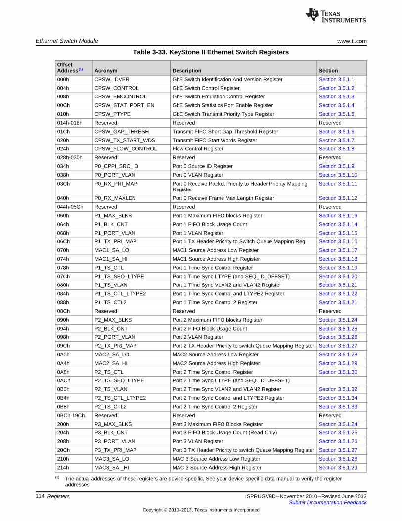
Ethernet Switch Module www.ti.com
114 SPRUGV9D–November 2010–Revised June 2013Submit Documentation Feedback
Copyright © 2010–2013, Texas Instruments Incorporated
Registers
(1) The actual addresses of these registers are device specific. See your device-specific data manual to verify the registeraddresses.
Table 3-33. KeyStone II Ethernet Switch Registers
OffsetAddress (1) Acronym Description Section000h CPSW_IDVER GbE Switch Identification And Version Register Section 3.5.1.1004h CPSW_CONTROL GbE Switch Control Register Section 3.5.1.2008h CPSW_EMCONTROL GbE Switch Emulation Control Register Section 3.5.1.300Ch CPSW_STAT_PORT_EN GbE Switch Statistics Port Enable Register Section 3.5.1.4010h CPSW_PTYPE GbE Switch Transmit Priority Type Register Section 3.5.1.5014h-018h Reserved Reserved Reserved01Ch CPSW_GAP_THRESH Transmit FIFO Short Gap Threshold Register Section 3.5.1.6020h CPSW_TX_START_WDS Transmit FIFO Start Words Register Section 3.5.1.7024h CPSW_FLOW_CONTROL Flow Control Register Section 3.5.1.8028h-030h Reserved Reserved Reserved034h P0_CPPI_SRC_ID Port 0 Source ID Register Section 3.5.1.9038h P0_PORT_VLAN Port 0 VLAN Register Section 3.5.1.1003Ch P0_RX_PRI_MAP Port 0 Receive Packet Priority to Header Priority Mapping
RegisterSection 3.5.1.11
040h P0_RX_MAXLEN Port 0 Receive Frame Max Length Register Section 3.5.1.12044h-05Ch Reserved Reserved Reserved060h P1_MAX_BLKS Port 1 Maximum FIFO blocks Register Section 3.5.1.13064h P1_BLK_CNT Port 1 FIFO Block Usage Count Section 3.5.1.14068h P1_PORT_VLAN Port 1 VLAN Register Section 3.5.1.1506Ch P1_TX_PRI_MAP Port 1 TX Header Priority to Switch Queue Mapping Reg Section 3.5.1.16070h MAC1_SA_LO MAC1 Source Address Low Register Section 3.5.1.17074h MAC1_SA_HI MAC1 Source Address High Register Section 3.5.1.18078h P1_TS_CTL Port 1 Time Sync Control Register Section 3.5.1.1907Ch P1_TS_SEQ_LTYPE Port 1 Time Sync LTYPE (and SEQ_ID_OFFSET) Section 3.5.1.20080h P1_TS_VLAN Port 1 Time Sync VLAN2 and VLAN2 Register Section 3.5.1.21084h P1_TS_CTL_LTYPE2 Port 1 Time Sync Control and LTYPE2 Register Section 3.5.1.22088h P1_TS_CTL2 Port 1 Time Sync Control 2 Register Section 3.5.1.2108Ch Reserved Reserved Reserved090h P2_MAX_BLKS Port 2 Maximum FIFO blocks Register Section 3.5.1.24094h P2_BLK_CNT Port 2 FIFO Block Usage Count Section 3.5.1.25098h P2_PORT_VLAN Port 2 VLAN Register Section 3.5.1.2609Ch P2_TX_PRI_MAP Port 2 TX Header Priority to switch Queue Mapping Register Section 3.5.1.270A0h MAC2_SA_LO MAC2 Source Address Low Register Section 3.5.1.280A4h MAC2_SA_HI MAC2 Source Address High Register Section 3.5.1.290A8h P2_TS_CTL Port 2 Time Sync Control Register Section 3.5.1.300ACh P2_TS_SEQ_LTYPE Port 2 Time Sync LTYPE (and SEQ_ID_OFFSET)0B0h P2_TS_VLAN Port 2 Time Sync VLAN2 and VLAN2 Register Section 3.5.1.320B4h P2_TS_CTL_LTYPE2 Port 2 Time Sync Control and LTYPE2 Register Section 3.5.1.340B8h P2_TS_CTL2 Port 2 Time Sync Control 2 Register Section 3.5.1.330BCh-19Ch Reserved Reserved Reserved200h P3_MAX_BLKS Port 3 Maximum FIFO Blocks Register Section 3.5.1.24204h P3_BLK_CNT Port 3 FIFO Block Usage Count (Read Only) Section 3.5.1.25208h P3_PORT_VLAN Port 3 VLAN Register Section 3.5.1.2620Ch P3_TX_PRI_MAP Port 3 TX Header Priority to switch Queue Mapping Register Section 3.5.1.27210h MAC3_SA_LO MAC 3 Source Address Low Register Section 3.5.1.28214h MAC3_SA _HI MAC 3 Source Address High Register Section 3.5.1.29
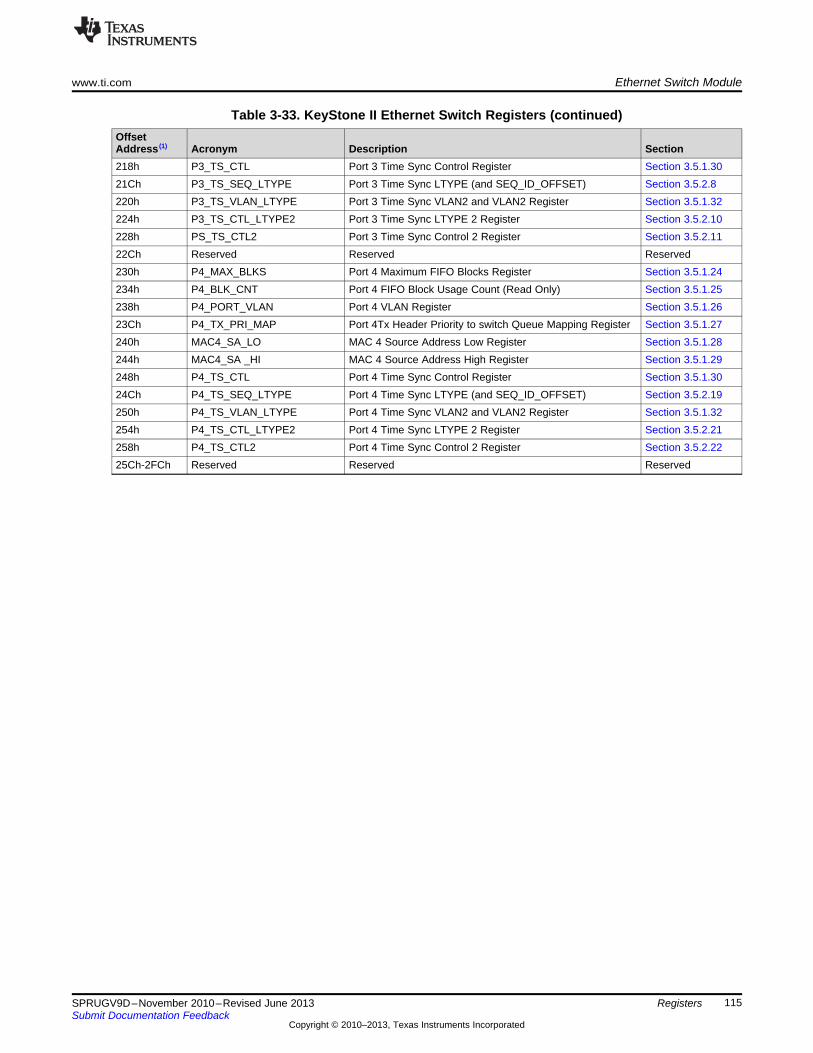
www.ti.com Ethernet Switch Module
115SPRUGV9D–November 2010–Revised June 2013Submit Documentation Feedback
Copyright © 2010–2013, Texas Instruments Incorporated
Registers
Table 3-33. KeyStone II Ethernet Switch Registers (continued)OffsetAddress (1) Acronym Description Section218h P3_TS_CTL Port 3 Time Sync Control Register Section 3.5.1.3021Ch P3_TS_SEQ_LTYPE Port 3 Time Sync LTYPE (and SEQ_ID_OFFSET) Section 3.5.2.8220h P3_TS_VLAN_LTYPE Port 3 Time Sync VLAN2 and VLAN2 Register Section 3.5.1.32224h P3_TS_CTL_LTYPE2 Port 3 Time Sync LTYPE 2 Register Section 3.5.2.10228h PS_TS_CTL2 Port 3 Time Sync Control 2 Register Section 3.5.2.1122Ch Reserved Reserved Reserved230h P4_MAX_BLKS Port 4 Maximum FIFO Blocks Register Section 3.5.1.24234h P4_BLK_CNT Port 4 FIFO Block Usage Count (Read Only) Section 3.5.1.25238h P4_PORT_VLAN Port 4 VLAN Register Section 3.5.1.2623Ch P4_TX_PRI_MAP Port 4Tx Header Priority to switch Queue Mapping Register Section 3.5.1.27240h MAC4_SA_LO MAC 4 Source Address Low Register Section 3.5.1.28244h MAC4_SA _HI MAC 4 Source Address High Register Section 3.5.1.29248h P4_TS_CTL Port 4 Time Sync Control Register Section 3.5.1.3024Ch P4_TS_SEQ_LTYPE Port 4 Time Sync LTYPE (and SEQ_ID_OFFSET) Section 3.5.2.19250h P4_TS_VLAN_LTYPE Port 4 Time Sync VLAN2 and VLAN2 Register Section 3.5.1.32254h P4_TS_CTL_LTYPE2 Port 4 Time Sync LTYPE 2 Register Section 3.5.2.21258h P4_TS_CTL2 Port 4 Time Sync Control 2 Register Section 3.5.2.2225Ch-2FCh Reserved Reserved Reserved
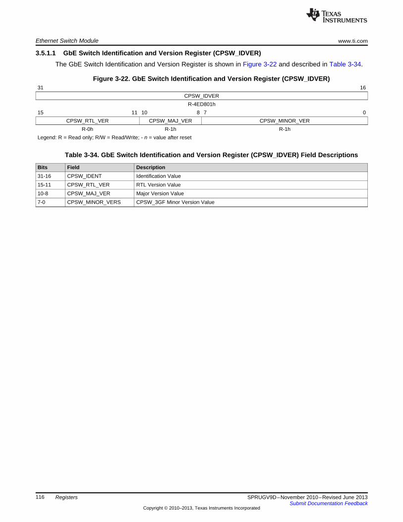
Ethernet Switch Module www.ti.com
116 SPRUGV9D–November 2010–Revised June 2013Submit Documentation Feedback
Copyright © 2010–2013, Texas Instruments Incorporated
Registers
3.5.1.1 GbE Switch Identification and Version Register (CPSW_IDVER)The GbE Switch Identification and Version Register is shown in Figure 3-22 and described in Table 3-34.
Figure 3-22. GbE Switch Identification and Version Register (CPSW_IDVER)31 16
CPSW_IDVERR-4ED801h
15 11 10 8 7 0CPSW_RTL_VER CPSW_MAJ_VER CPSW_MINOR_VER
R-0h R-1h R-1hLegend: R = Read only; R/W = Read/Write; - n = value after reset
Table 3-34. GbE Switch Identification and Version Register (CPSW_IDVER) Field Descriptions
Bits Field Description31-16 CPSW_IDENT Identification Value15-11 CPSW_RTL_VER RTL Version Value10-8 CPSW_MAJ_VER Major Version Value7-0 CPSW_MINOR_VERS CPSW_3GF Minor Version Value
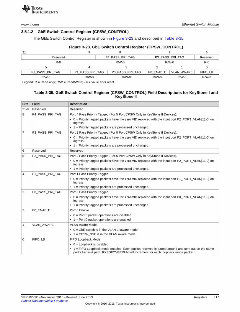
www.ti.com Ethernet Switch Module
117SPRUGV9D–November 2010–Revised June 2013Submit Documentation Feedback
Copyright © 2010–2013, Texas Instruments Incorporated
Registers
3.5.1.2 GbE Switch Control Register (CPSW_CONTROL)The GbE Switch Control Register is shown in Figure 3-23 and described in Table 3-35.
Figure 3-23. GbE Switch Control Register (CPSW_CONTROL)31 9 8 7 6
Reserved P4_PASS_PRI_TAG P3_PASS_PRI_TAG ReservedR-0 R/W-0 R/W-0 R-0
5 4 3 2 1 0P2_PASS_PRI_TAG P1_PASS_PRI_TAG P0_PASS_PRI_TAG P0_ENABLE VLAN_AWARE FIFO_LB
R/W-0 R/W-0 R/W-0 R/W-0 R/W-0 R/W-0Legend: R = Read only; R/W = Read/Write; - n = value after reset
Table 3-35. GbE Switch Control Register (CPSW_CONTROL) Field Descriptions for KeyStone I andKeyStone II
Bits Field Description31-9 Reserved Reserved8 P4_PASS_PRI_TAG Port 4 Pass Priority Tagged (For 5 Port CPSW Only in KeyStone II Devices).
• 0 = Priority tagged packets have the zero VID replaced with the input port P2_PORT_VLAN[11-0] oningress.
• 1 = Priority tagged packets are processed unchanged.7 P3_PASS_PRI_TAG Port 3 Pass Priority Tagged (For 5 Port CPSW Only in KeyStone II Devices).
• 0 = Priority tagged packets have the zero VID replaced with the input port P2_PORT_VLAN[11-0] oningress.
• 1 = Priority tagged packets are processed unchanged.6 Reserved Reserved5 P2_PASS_PRI_TAG Port 2 Pass Priority Tagged (For 5 Port CPSW Only in KeyStone II Devices).
• 0 = Priority tagged packets have the zero VID replaced with the input port P2_PORT_VLAN[11-0] oningress.
• 1 = Priority tagged packets are processed unchanged.4 P1_PASS_PRI_TAG Port 1 Pass Priority Tagged.
• 0 = Priority tagged packets have the zero VID replaced with the input port P1_PORT_VLAN[11-0] oningress.
• 1 = Priority tagged packets are processed unchanged.3 P0_PASS_PRI_TAG Port 0 Pass Priority Tagged.
• 0 = Priority tagged packets have the zero VID replaced with the input port P0_PORT_VLAN[11-0] oningress.
• 1 = Priority tagged packets are processed unchanged.2 P0_ENABLE Port 0 Enable.
• 0 = Port 0 packet operations are disabled.• 1 = Port 0 packet operations are enabled.
1 VLAN_AWARE VLAN Aware Mode.• 0 = GbE switch is in the VLAN unaware mode.• 1 = CPSW_3GF is in the VLAN aware mode.
0 FIFO_LB FIFO Loopback Mode.• 0 = Loopback is disabled• 1 = FIFO Loopback mode enabled. Each packet received is turned around and sent out on the same
port’s transmit path. RXSOFOVERRUN will increment for each loopback mode packet.
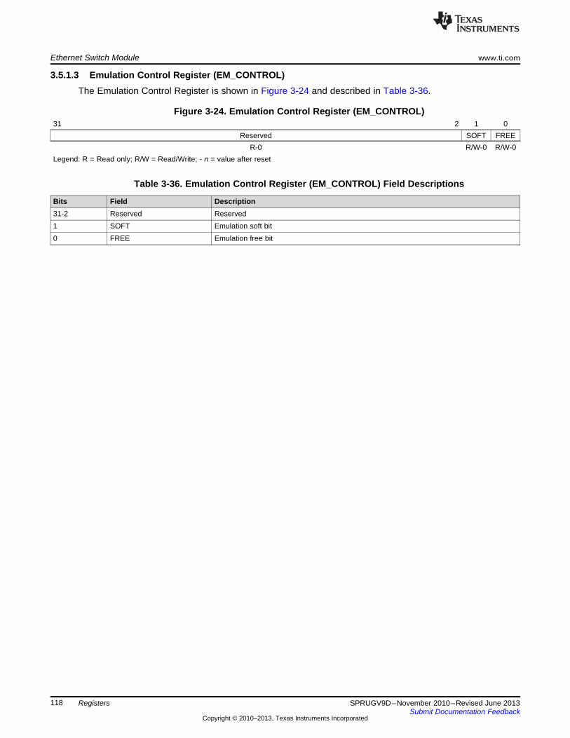
Ethernet Switch Module www.ti.com
118 SPRUGV9D–November 2010–Revised June 2013Submit Documentation Feedback
Copyright © 2010–2013, Texas Instruments Incorporated
Registers
3.5.1.3 Emulation Control Register (EM_CONTROL)The Emulation Control Register is shown in Figure 3-24 and described in Table 3-36.
Figure 3-24. Emulation Control Register (EM_CONTROL)31 2 1 0
Reserved SOFT FREER-0 R/W-0 R/W-0
Legend: R = Read only; R/W = Read/Write; - n = value after reset
Table 3-36. Emulation Control Register (EM_CONTROL) Field Descriptions
Bits Field Description31-2 Reserved Reserved1 SOFT Emulation soft bit0 FREE Emulation free bit
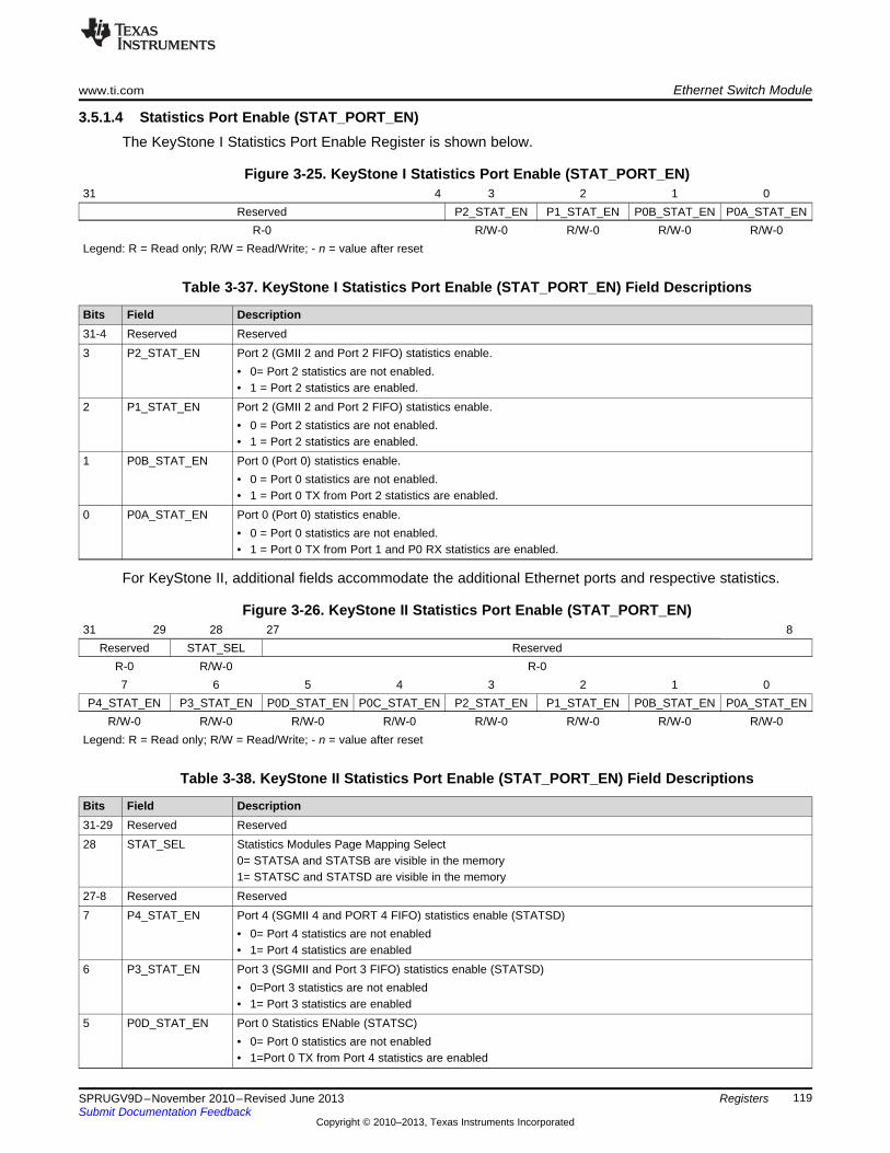
www.ti.com Ethernet Switch Module
119SPRUGV9D–November 2010–Revised June 2013Submit Documentation Feedback
Copyright © 2010–2013, Texas Instruments Incorporated
Registers
3.5.1.4 Statistics Port Enable (STAT_PORT_EN)The KeyStone I Statistics Port Enable Register is shown below.
Figure 3-25. KeyStone I Statistics Port Enable (STAT_PORT_EN)31 4 3 2 1 0
Reserved P2_STAT_EN P1_STAT_EN P0B_STAT_EN P0A_STAT_ENR-0 R/W-0 R/W-0 R/W-0 R/W-0
Legend: R = Read only; R/W = Read/Write; - n = value after reset
Table 3-37. KeyStone I Statistics Port Enable (STAT_PORT_EN) Field Descriptions
Bits Field Description31-4 Reserved Reserved3 P2_STAT_EN Port 2 (GMII 2 and Port 2 FIFO) statistics enable.
• 0= Port 2 statistics are not enabled.• 1 = Port 2 statistics are enabled.
2 P1_STAT_EN Port 2 (GMII 2 and Port 2 FIFO) statistics enable.• 0 = Port 2 statistics are not enabled.• 1 = Port 2 statistics are enabled.
1 P0B_STAT_EN Port 0 (Port 0) statistics enable.• 0 = Port 0 statistics are not enabled.• 1 = Port 0 TX from Port 2 statistics are enabled.
0 P0A_STAT_EN Port 0 (Port 0) statistics enable.• 0 = Port 0 statistics are not enabled.• 1 = Port 0 TX from Port 1 and P0 RX statistics are enabled.
For KeyStone II, additional fields accommodate the additional Ethernet ports and respective statistics.
Figure 3-26. KeyStone II Statistics Port Enable (STAT_PORT_EN)31 29 28 27 8
Reserved STAT_SEL ReservedR-0 R/W-0 R-07 6 5 4 3 2 1 0
P4_STAT_EN P3_STAT_EN P0D_STAT_EN P0C_STAT_EN P2_STAT_EN P1_STAT_EN P0B_STAT_EN P0A_STAT_ENR/W-0 R/W-0 R/W-0 R/W-0 R/W-0 R/W-0 R/W-0 R/W-0
Legend: R = Read only; R/W = Read/Write; - n = value after reset
Table 3-38. KeyStone II Statistics Port Enable (STAT_PORT_EN) Field Descriptions
Bits Field Description31-29 Reserved Reserved28 STAT_SEL Statistics Modules Page Mapping Select
0= STATSA and STATSB are visible in the memory1= STATSC and STATSD are visible in the memory
27-8 Reserved Reserved7 P4_STAT_EN Port 4 (SGMII 4 and PORT 4 FIFO) statistics enable (STATSD)
• 0= Port 4 statistics are not enabled• 1= Port 4 statistics are enabled
6 P3_STAT_EN Port 3 (SGMII and Port 3 FIFO) statistics enable (STATSD)• 0=Port 3 statistics are not enabled• 1= Port 3 statistics are enabled
5 P0D_STAT_EN Port 0 Statistics ENable (STATSC)• 0= Port 0 statistics are not enabled• 1=Port 0 TX from Port 4 statistics are enabled
Ethernet Switch Module www.ti.com
120 SPRUGV9D–November 2010–Revised June 2013Submit Documentation Feedback
Copyright © 2010–2013, Texas Instruments Incorporated
Registers
Table 3-38. KeyStone II Statistics Port Enable (STAT_PORT_EN) Field Descriptions (continued)Bits Field Description4 P0C_STAT_EN Port Statistics Enable (STATSC)
• 0=Port 0 Statistics not enabled• 1= Port 0 TX from Port 3statistics are enabled
3 P2_STAT_EN Port 2 (GMII 2 and Port 2 FIFO) Statistics Enable (STATSB).• 0= Port 2 statistics are not enabled.• 1 = Port 2 statistics are enabled.
2 P1_STAT_EN Port 2 (GMII 1and Port 1 FIFO) Statistics Enable (STATSB).• 0 = Port 1statistics are not enabled.• 1 = Port 1statistics are enabled.
1 P0B_STAT_EN Port 0 (Port 0) Statistics Enable (STATSA).• 0 =Port 0 statistics are not enabled.• 1 =Port 0 TX from Port 2 statistics are enabled.
0 P0A_STAT_EN Port 0 (Port 0) Statistics Enable (STATSA).• 0 =Port 0 statistics are not enabled.• 1 =Port 0 TX from Port 1 and P0 RX statistics are enabled.
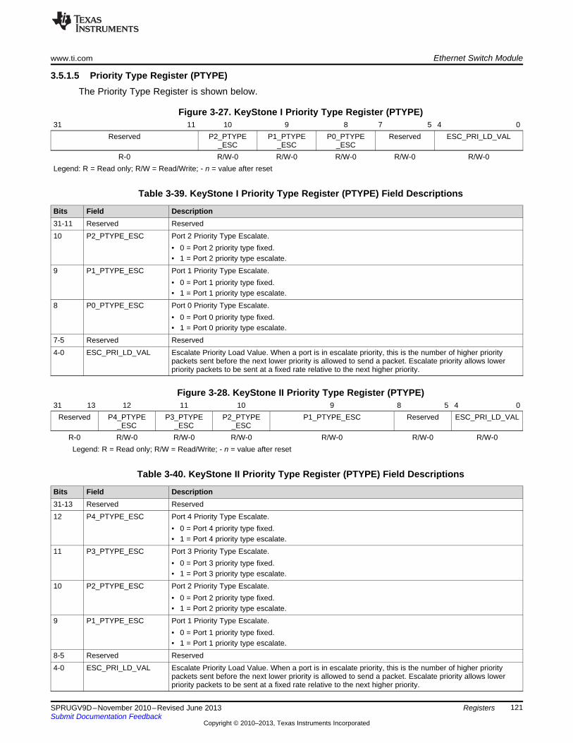
www.ti.com Ethernet Switch Module
121SPRUGV9D–November 2010–Revised June 2013Submit Documentation Feedback
Copyright © 2010–2013, Texas Instruments Incorporated
Registers
3.5.1.5 Priority Type Register (PTYPE)The Priority Type Register is shown below.
Figure 3-27. KeyStone I Priority Type Register (PTYPE)31 11 10 9 8 7 5 4 0
Reserved P2_PTYPE_ESC
P1_PTYPE_ESC
P0_PTYPE_ESC
Reserved ESC_PRI_LD_VAL
R-0 R/W-0 R/W-0 R/W-0 R/W-0 R/W-0Legend: R = Read only; R/W = Read/Write; - n = value after reset
Table 3-39. KeyStone I Priority Type Register (PTYPE) Field Descriptions
Bits Field Description31-11 Reserved Reserved10 P2_PTYPE_ESC Port 2 Priority Type Escalate.
• 0 = Port 2 priority type fixed.• 1 = Port 2 priority type escalate.
9 P1_PTYPE_ESC Port 1 Priority Type Escalate.• 0 = Port 1 priority type fixed.• 1 = Port 1 priority type escalate.
8 P0_PTYPE_ESC Port 0 Priority Type Escalate.• 0 = Port 0 priority type fixed.• 1 = Port 0 priority type escalate.
7-5 Reserved Reserved4-0 ESC_PRI_LD_VAL Escalate Priority Load Value. When a port is in escalate priority, this is the number of higher priority
packets sent before the next lower priority is allowed to send a packet. Escalate priority allows lowerpriority packets to be sent at a fixed rate relative to the next higher priority.
Figure 3-28. KeyStone II Priority Type Register (PTYPE)31 13 12 11 10 9 8 5 4 0
Reserved P4_PTYPE_ESC
P3_PTYPE_ESC
P2_PTYPE_ESC
P1_PTYPE_ESC Reserved ESC_PRI_LD_VAL
R-0 R/W-0 R/W-0 R/W-0 R/W-0 R/W-0 R/W-0Legend: R = Read only; R/W = Read/Write; - n = value after reset
Table 3-40. KeyStone II Priority Type Register (PTYPE) Field Descriptions
Bits Field Description31-13 Reserved Reserved12 P4_PTYPE_ESC Port 4 Priority Type Escalate.
• 0 = Port 4 priority type fixed.• 1 = Port 4 priority type escalate.
11 P3_PTYPE_ESC Port 3 Priority Type Escalate.• 0 = Port 3 priority type fixed.• 1 = Port 3 priority type escalate.
10 P2_PTYPE_ESC Port 2 Priority Type Escalate.• 0 = Port 2 priority type fixed.• 1 = Port 2 priority type escalate.
9 P1_PTYPE_ESC Port 1 Priority Type Escalate.• 0 = Port 1 priority type fixed.• 1 = Port 1 priority type escalate.
8-5 Reserved Reserved4-0 ESC_PRI_LD_VAL Escalate Priority Load Value. When a port is in escalate priority, this is the number of higher priority
packets sent before the next lower priority is allowed to send a packet. Escalate priority allows lowerpriority packets to be sent at a fixed rate relative to the next higher priority.
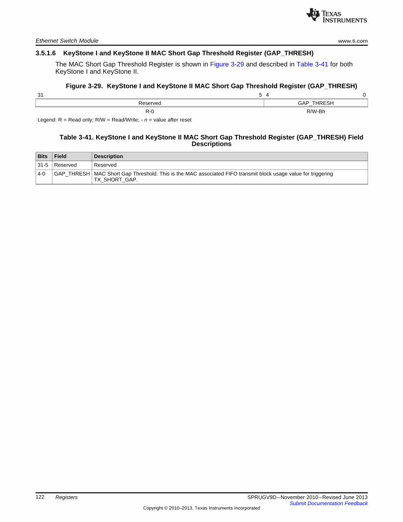
Ethernet Switch Module www.ti.com
122 SPRUGV9D–November 2010–Revised June 2013Submit Documentation Feedback
Copyright © 2010–2013, Texas Instruments Incorporated
Registers
3.5.1.6 KeyStone I and KeyStone II MAC Short Gap Threshold Register (GAP_THRESH)The MAC Short Gap Threshold Register is shown in Figure 3-29 and described in Table 3-41 for bothKeyStone I and KeyStone II.
Figure 3-29. KeyStone I and KeyStone II MAC Short Gap Threshold Register (GAP_THRESH)31 5 4 0
Reserved GAP_THRESHR-0 R/W-Bh
Legend: R = Read only; R/W = Read/Write; - n = value after reset
Table 3-41. KeyStone I and KeyStone II MAC Short Gap Threshold Register (GAP_THRESH) FieldDescriptions
Bits Field Description31-5 Reserved Reserved4-0 GAP_THRESH MAC Short Gap Threshold. This is the MAC associated FIFO transmit block usage value for triggering
TX_SHORT_GAP.
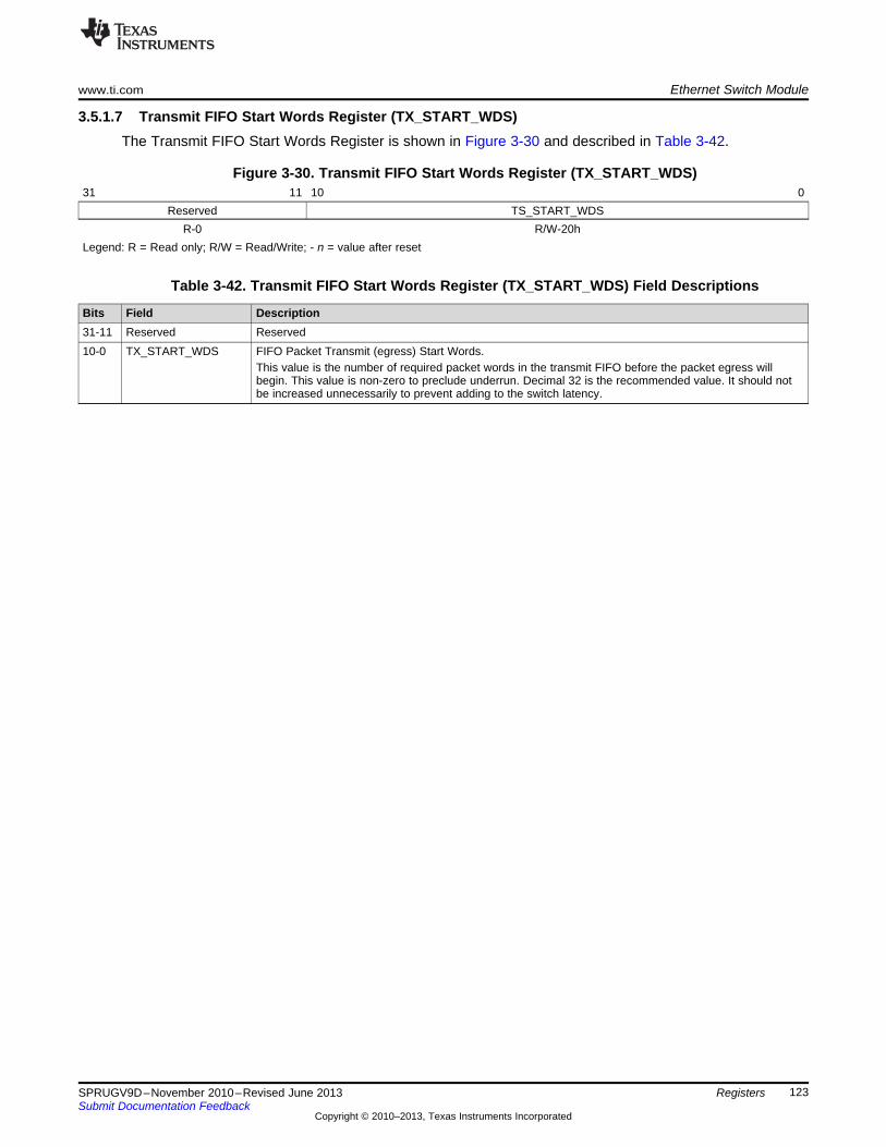
www.ti.com Ethernet Switch Module
123SPRUGV9D–November 2010–Revised June 2013Submit Documentation Feedback
Copyright © 2010–2013, Texas Instruments Incorporated
Registers
3.5.1.7 Transmit FIFO Start Words Register (TX_START_WDS)The Transmit FIFO Start Words Register is shown in Figure 3-30 and described in Table 3-42.
Figure 3-30. Transmit FIFO Start Words Register (TX_START_WDS)31 11 10 0
Reserved TS_START_WDSR-0 R/W-20h
Legend: R = Read only; R/W = Read/Write; - n = value after reset
Table 3-42. Transmit FIFO Start Words Register (TX_START_WDS) Field Descriptions
Bits Field Description31-11 Reserved Reserved10-0 TX_START_WDS FIFO Packet Transmit (egress) Start Words.
This value is the number of required packet words in the transmit FIFO before the packet egress willbegin. This value is non-zero to preclude underrun. Decimal 32 is the recommended value. It should notbe increased unnecessarily to prevent adding to the switch latency.
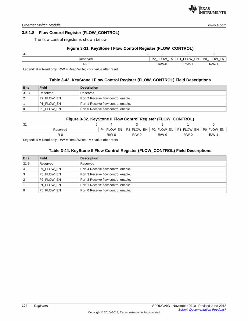
Ethernet Switch Module www.ti.com
124 SPRUGV9D–November 2010–Revised June 2013Submit Documentation Feedback
Copyright © 2010–2013, Texas Instruments Incorporated
Registers
3.5.1.8 Flow Control Register (FLOW_CONTROL)The flow control register is shown below.
Figure 3-31. KeyStone I Flow Control Register (FLOW_CONTROL)31 3 2 1 0
Reserved P2_FLOW_EN P1_FLOW_EN P0_FLOW_ENR-0 R/W-0 R/W-0 R/W-1
Legend: R = Read only; R/W = Read/Write; - n = value after reset
Table 3-43. KeyStone I Flow Control Register (FLOW_CONTROL) Field Descriptions
Bits Field Description31-3 Reserved Reserved2 P2_FLOW_EN Port 2 Receive flow control enable.1 P1_FLOW_EN Port 1 Receive flow control enable.0 P0_FLOW_EN Port 0 Receive flow control enable.
Figure 3-32. KeyStone II Flow Control Register (FLOW_CONTROL)31 5 4 3 2 1 0
Reserved P4_FLOW_EN P3_FLOW_EN P2_FLOW_EN P1_FLOW_EN P0_FLOW_ENR-0 R/W-0 R/W-0 R/W-0 R/W-0 R/W-1
Legend: R = Read only; R/W = Read/Write; - n = value after reset
Table 3-44. KeyStone II Flow Control Register (FLOW_CONTROL) Field Descriptions
Bits Field Description31-5 Reserved Reserved4 P4_FLOW_EN Port 4 Receive flow control enable.3 P3_FLOW_EN Port 3 Receive flow control enable.2 P2_FLOW_EN Port 2 Receive flow control enable.1 P1_FLOW_EN Port 1 Receive flow control enable.0 P0_FLOW_EN Port 0 Receive flow control enable.
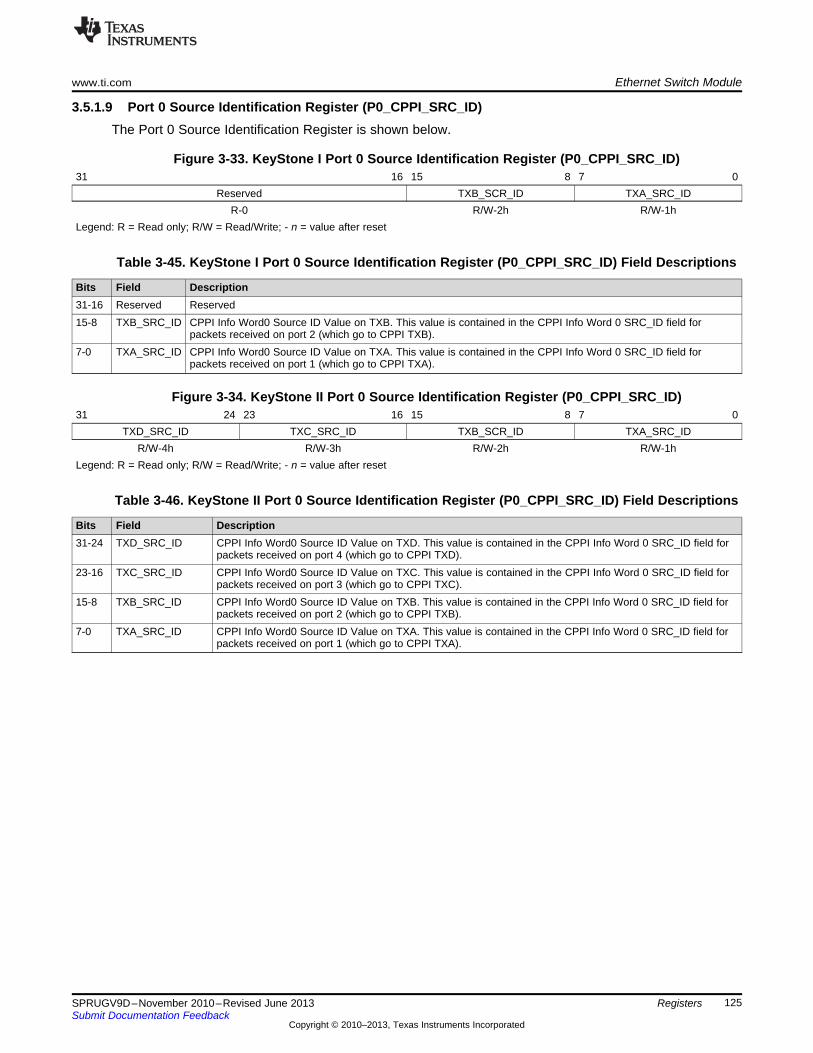
www.ti.com Ethernet Switch Module
125SPRUGV9D–November 2010–Revised June 2013Submit Documentation Feedback
Copyright © 2010–2013, Texas Instruments Incorporated
Registers
3.5.1.9 Port 0 Source Identification Register (P0_CPPI_SRC_ID)The Port 0 Source Identification Register is shown below.
Figure 3-33. KeyStone I Port 0 Source Identification Register (P0_CPPI_SRC_ID)31 16 15 8 7 0
Reserved TXB_SCR_ID TXA_SRC_IDR-0 R/W-2h R/W-1h
Legend: R = Read only; R/W = Read/Write; - n = value after reset
Table 3-45. KeyStone I Port 0 Source Identification Register (P0_CPPI_SRC_ID) Field Descriptions
Bits Field Description31-16 Reserved Reserved15-8 TXB_SRC_ID CPPI Info Word0 Source ID Value on TXB. This value is contained in the CPPI Info Word 0 SRC_ID field for
packets received on port 2 (which go to CPPI TXB).7-0 TXA_SRC_ID CPPI Info Word0 Source ID Value on TXA. This value is contained in the CPPI Info Word 0 SRC_ID field for
packets received on port 1 (which go to CPPI TXA).
Figure 3-34. KeyStone II Port 0 Source Identification Register (P0_CPPI_SRC_ID)31 24 23 16 15 8 7 0
TXD_SRC_ID TXC_SRC_ID TXB_SCR_ID TXA_SRC_IDR/W-4h R/W-3h R/W-2h R/W-1h
Legend: R = Read only; R/W = Read/Write; - n = value after reset
Table 3-46. KeyStone II Port 0 Source Identification Register (P0_CPPI_SRC_ID) Field Descriptions
Bits Field Description31-24 TXD_SRC_ID CPPI Info Word0 Source ID Value on TXD. This value is contained in the CPPI Info Word 0 SRC_ID field for
packets received on port 4 (which go to CPPI TXD).23-16 TXC_SRC_ID CPPI Info Word0 Source ID Value on TXC. This value is contained in the CPPI Info Word 0 SRC_ID field for
packets received on port 3 (which go to CPPI TXC).15-8 TXB_SRC_ID CPPI Info Word0 Source ID Value on TXB. This value is contained in the CPPI Info Word 0 SRC_ID field for
packets received on port 2 (which go to CPPI TXB).7-0 TXA_SRC_ID CPPI Info Word0 Source ID Value on TXA. This value is contained in the CPPI Info Word 0 SRC_ID field for
packets received on port 1 (which go to CPPI TXA).
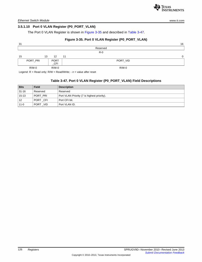
Ethernet Switch Module www.ti.com
126 SPRUGV9D–November 2010–Revised June 2013Submit Documentation Feedback
Copyright © 2010–2013, Texas Instruments Incorporated
Registers
3.5.1.10 Port 0 VLAN Register (P0_PORT_VLAN)The Port 0 VLAN Register is shown in Figure 3-35 and described in Table 3-47.
Figure 3-35. Port 0 VLAN Register (P0_PORT_VLAN)31 16
ReservedR-0
15 13 12 11 0PORT_PRI PORT
_CFIPORT_VID
R/W-0 R/W-0 R/W-0Legend: R = Read only; R/W = Read/Write; - n = value after reset
Table 3-47. Port 0 VLAN Register (P0_PORT_VLAN) Field Descriptions
Bits Field Description31-16 Reserved Reserved15-13 PORT_PRI Port VLAN Priority (7 is highest priority).12 PORT _CFI Port CFI bit.11-0 PORT _VID Port VLAN ID.
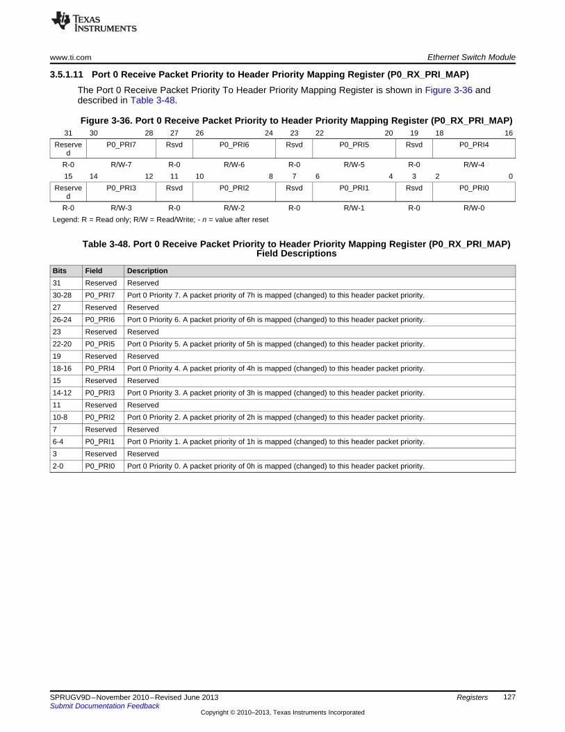
www.ti.com Ethernet Switch Module
127SPRUGV9D–November 2010–Revised June 2013Submit Documentation Feedback
Copyright © 2010–2013, Texas Instruments Incorporated
Registers
3.5.1.11 Port 0 Receive Packet Priority to Header Priority Mapping Register (P0_RX_PRI_MAP)The Port 0 Receive Packet Priority To Header Priority Mapping Register is shown in Figure 3-36 anddescribed in Table 3-48.
Figure 3-36. Port 0 Receive Packet Priority to Header Priority Mapping Register (P0_RX_PRI_MAP)31 30 28 27 26 24 23 22 20 19 18 16
Reserved
P0_PRI7 Rsvd P0_PRI6 Rsvd P0_PRI5 Rsvd P0_PRI4
R-0 R/W-7 R-0 R/W-6 R-0 R/W-5 R-0 R/W-415 14 12 11 10 8 7 6 4 3 2 0
Reserved
P0_PRI3 Rsvd P0_PRI2 Rsvd P0_PRI1 Rsvd P0_PRI0
R-0 R/W-3 R-0 R/W-2 R-0 R/W-1 R-0 R/W-0Legend: R = Read only; R/W = Read/Write; - n = value after reset
Table 3-48. Port 0 Receive Packet Priority to Header Priority Mapping Register (P0_RX_PRI_MAP)Field Descriptions
Bits Field Description31 Reserved Reserved30-28 P0_PRI7 Port 0 Priority 7. A packet priority of 7h is mapped (changed) to this header packet priority.27 Reserved Reserved26-24 P0_PRI6 Port 0 Priority 6. A packet priority of 6h is mapped (changed) to this header packet priority.23 Reserved Reserved22-20 P0_PRI5 Port 0 Priority 5. A packet priority of 5h is mapped (changed) to this header packet priority.19 Reserved Reserved18-16 P0_PRI4 Port 0 Priority 4. A packet priority of 4h is mapped (changed) to this header packet priority.15 Reserved Reserved14-12 P0_PRI3 Port 0 Priority 3. A packet priority of 3h is mapped (changed) to this header packet priority.11 Reserved Reserved10-8 P0_PRI2 Port 0 Priority 2. A packet priority of 2h is mapped (changed) to this header packet priority.7 Reserved Reserved6-4 P0_PRI1 Port 0 Priority 1. A packet priority of 1h is mapped (changed) to this header packet priority.3 Reserved Reserved2-0 P0_PRI0 Port 0 Priority 0. A packet priority of 0h is mapped (changed) to this header packet priority.
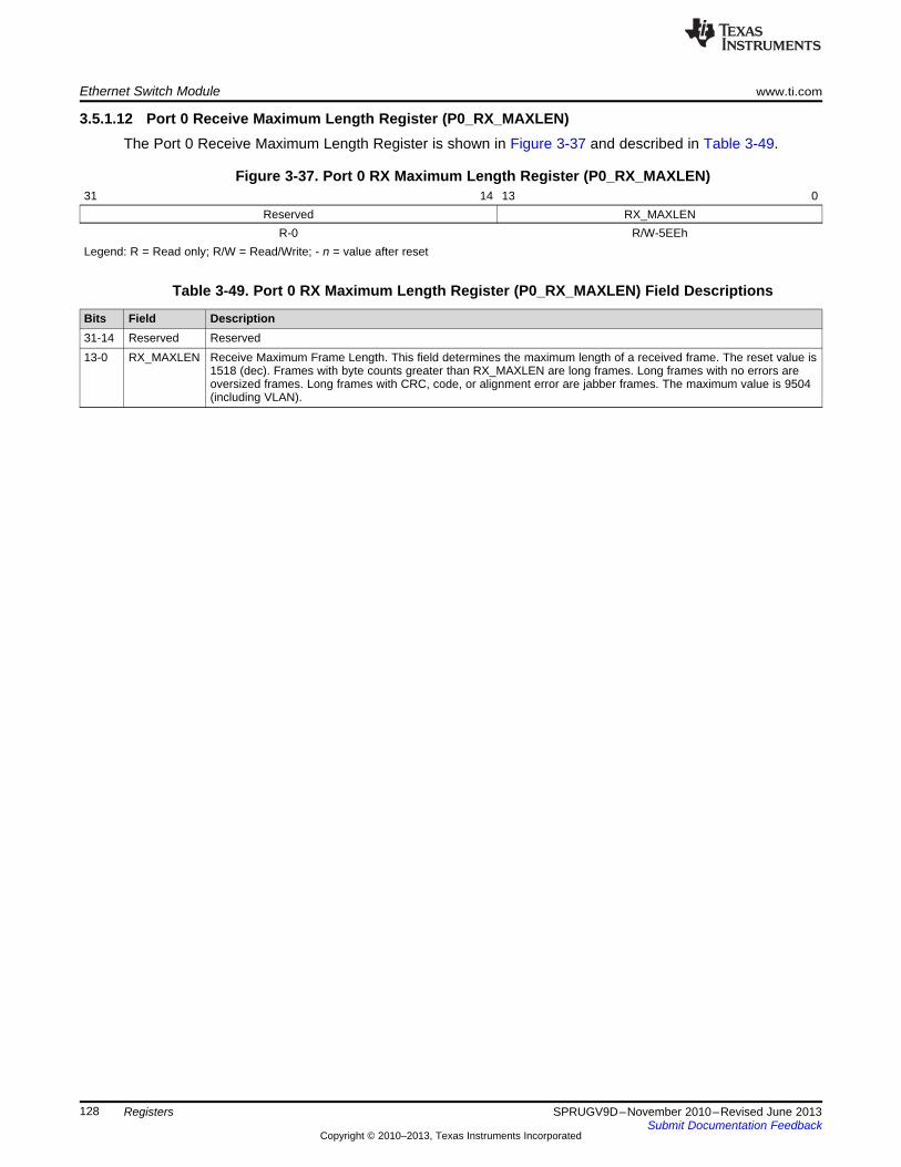
Ethernet Switch Module www.ti.com
128 SPRUGV9D–November 2010–Revised June 2013Submit Documentation Feedback
Copyright © 2010–2013, Texas Instruments Incorporated
Registers
3.5.1.12 Port 0 Receive Maximum Length Register (P0_RX_MAXLEN)The Port 0 Receive Maximum Length Register is shown in Figure 3-37 and described in Table 3-49.
Figure 3-37. Port 0 RX Maximum Length Register (P0_RX_MAXLEN)31 14 13 0
Reserved RX_MAXLENR-0 R/W-5EEh
Legend: R = Read only; R/W = Read/Write; - n = value after reset
Table 3-49. Port 0 RX Maximum Length Register (P0_RX_MAXLEN) Field Descriptions
Bits Field Description31-14 Reserved Reserved13-0 RX_MAXLEN Receive Maximum Frame Length. This field determines the maximum length of a received frame. The reset value is
1518 (dec). Frames with byte counts greater than RX_MAXLEN are long frames. Long frames with no errors areoversized frames. Long frames with CRC, code, or alignment error are jabber frames. The maximum value is 9504(including VLAN).
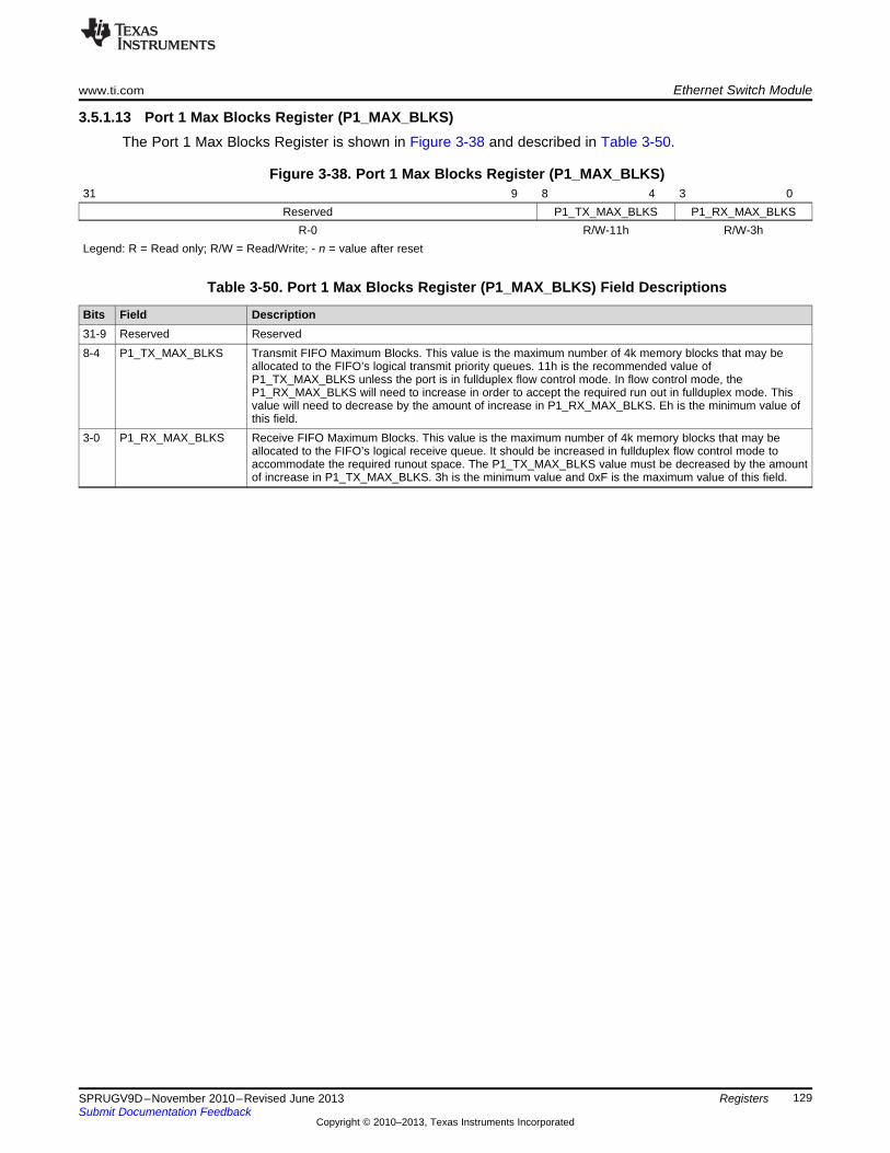
www.ti.com Ethernet Switch Module
129SPRUGV9D–November 2010–Revised June 2013Submit Documentation Feedback
Copyright © 2010–2013, Texas Instruments Incorporated
Registers
3.5.1.13 Port 1 Max Blocks Register (P1_MAX_BLKS)The Port 1 Max Blocks Register is shown in Figure 3-38 and described in Table 3-50.
Figure 3-38. Port 1 Max Blocks Register (P1_MAX_BLKS)31 9 8 4 3 0
Reserved P1_TX_MAX_BLKS P1_RX_MAX_BLKSR-0 R/W-11h R/W-3h
Legend: R = Read only; R/W = Read/Write; - n = value after reset
Table 3-50. Port 1 Max Blocks Register (P1_MAX_BLKS) Field Descriptions
Bits Field Description31-9 Reserved Reserved8-4 P1_TX_MAX_BLKS Transmit FIFO Maximum Blocks. This value is the maximum number of 4k memory blocks that may be
allocated to the FIFO’s logical transmit priority queues. 11h is the recommended value ofP1_TX_MAX_BLKS unless the port is in fullduplex flow control mode. In flow control mode, theP1_RX_MAX_BLKS will need to increase in order to accept the required run out in fullduplex mode. Thisvalue will need to decrease by the amount of increase in P1_RX_MAX_BLKS. Eh is the minimum value ofthis field.
3-0 P1_RX_MAX_BLKS Receive FIFO Maximum Blocks. This value is the maximum number of 4k memory blocks that may beallocated to the FIFO’s logical receive queue. It should be increased in fullduplex flow control mode toaccommodate the required runout space. The P1_TX_MAX_BLKS value must be decreased by the amountof increase in P1_TX_MAX_BLKS. 3h is the minimum value and 0xF is the maximum value of this field.
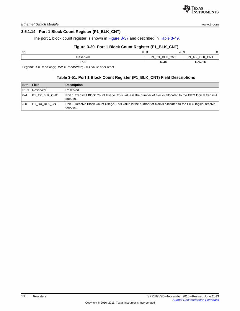
Ethernet Switch Module www.ti.com
130 SPRUGV9D–November 2010–Revised June 2013Submit Documentation Feedback
Copyright © 2010–2013, Texas Instruments Incorporated
Registers
3.5.1.14 Port 1 Block Count Register (P1_BLK_CNT)The port 1 block count register is shown in Figure 3-37 and described in Table 3-49.
Figure 3-39. Port 1 Block Count Register (P1_BLK_CNT)31 9 8 4 3 0
Reserved P1_TX_BLK_CNT P1_RX_BLK_CNTR-0 R-4h R/W-1h
Legend: R = Read only; R/W = Read/Write; - n = value after reset
Table 3-51. Port 1 Block Count Register (P1_BLK_CNT) Field Descriptions
Bits Field Description31-9 Reserved Reserved8-4 P1_TX_BLK_CNT Port 1 Transmit Block Count Usage. This value is the number of blocks allocated to the FIFO logical transmit
queues.3-0 P1_RX_BLK_CNT Port 1 Receive Block Count Usage. This value is the number of blocks allocated to the FIFO logical receive
queues.
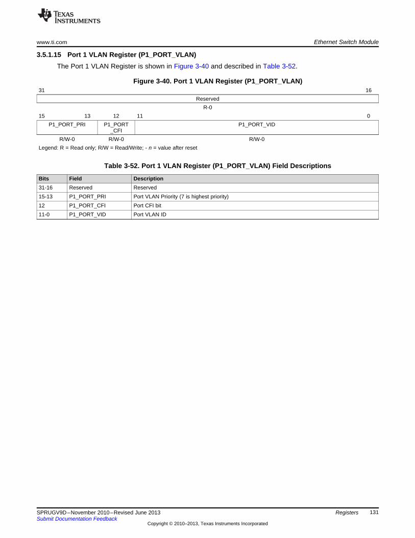
www.ti.com Ethernet Switch Module
131SPRUGV9D–November 2010–Revised June 2013Submit Documentation Feedback
Copyright © 2010–2013, Texas Instruments Incorporated
Registers
3.5.1.15 Port 1 VLAN Register (P1_PORT_VLAN)The Port 1 VLAN Register is shown in Figure 3-40 and described in Table 3-52.
Figure 3-40. Port 1 VLAN Register (P1_PORT_VLAN)31 16
ReservedR-0
15 13 12 11 0P1_PORT_PRI P1_PORT
_CFIP1_PORT_VID
R/W-0 R/W-0 R/W-0Legend: R = Read only; R/W = Read/Write; - n = value after reset
Table 3-52. Port 1 VLAN Register (P1_PORT_VLAN) Field Descriptions
Bits Field Description31-16 Reserved Reserved15-13 P1_PORT_PRI Port VLAN Priority (7 is highest priority)12 P1_PORT_CFI Port CFI bit11-0 P1_PORT_VID Port VLAN ID
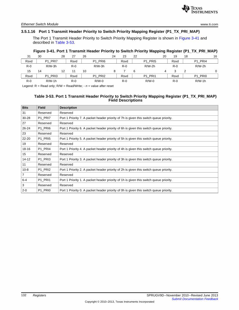
Ethernet Switch Module www.ti.com
132 SPRUGV9D–November 2010–Revised June 2013Submit Documentation Feedback
Copyright © 2010–2013, Texas Instruments Incorporated
Registers
3.5.1.16 Port 1 Transmit Header Priority to Switch Priority Mapping Register (P1_TX_PRI_MAP)The Port 1 Transmit Header Priority to Switch Priority Mapping Register is shown in Figure 3-41 anddescribed in Table 3-53.
Figure 3-41. Port 1 Transmit Header Priority to Switch Priority Mapping Register (P1_TX_PRI_MAP)31 30 28 27 26 24 23 22 20 19 18 16
Rsvd P1_PRI7 Rsvd P1_PRI6 Rsvd P1_PRI5 Rsvd P1_PRI4R-0 R/W-3h R-0 R/W-3h R-0 R/W-2h R-0 R/W-2h15 14 12 11 10 8 7 6 4 3 2 0
Rsvd P1_PRI3 Rsvd P1_PRI2 Rsvd P1_PRI1 Rsvd P1_PRI0R-0 R/W-1h R-0 R/W-0 R-0 R/W-0 R-0 R/W-1h
Legend: R = Read only; R/W = Read/Write; - n = value after reset
Table 3-53. Port 1 Transmit Header Priority to Switch Priority Mapping Register (P1_TX_PRI_MAP)Field Descriptions
Bits Field Description31 Reserved Reserved30-28 P1_PRI7 Port 1 Priority 7. A packet header priority of 7h is given this switch queue priority.27 Reserved Reserved26-24 P1_PRI6 Port 1 Priority 6. A packet header priority of 6h is given this switch queue priority.23 Reserved Reserved22-20 P1_PRI5 Port 1 Priority 5. A packet header priority of 5h is given this switch queue priority.19 Reserved Reserved18-16 P1_PRI4 Port 1 Priority 4. A packet header priority of 4h is given this switch queue priority.15 Reserved Reserved14-12 P1_PRI3 Port 1 Priority 3. A packet header priority of 3h is given this switch queue priority.11 Reserved Reserved10-8 P1_PRI2 Port 1 Priority 2. A packet header priority of 2h is given this switch queue priority.7 Reserved Reserved6-4 P1_PRI1 Port 1 Priority 1. A packet header priority of 1h is given this switch queue priority.3 Reserved Reserved2-0 P1_PRI0 Port 1 Priority 0. A packet header priority of 0h is given this switch queue priority.
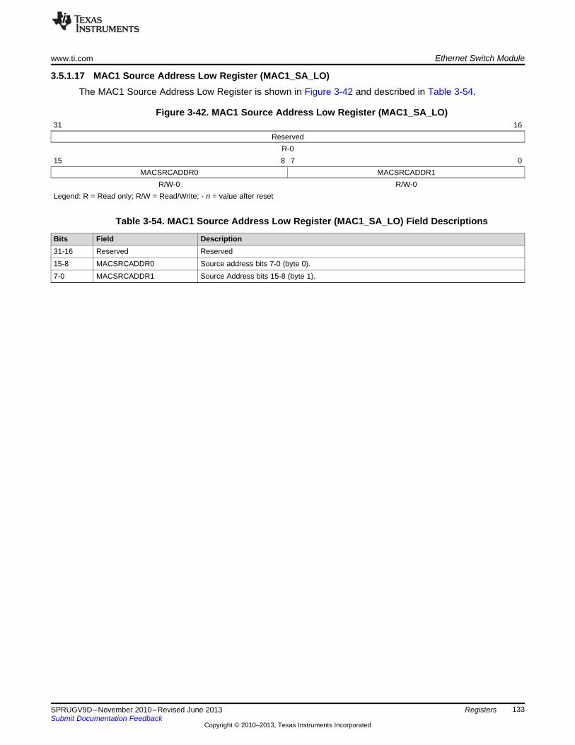
www.ti.com Ethernet Switch Module
133SPRUGV9D–November 2010–Revised June 2013Submit Documentation Feedback
Copyright © 2010–2013, Texas Instruments Incorporated
Registers
3.5.1.17 MAC1 Source Address Low Register (MAC1_SA_LO)The MAC1 Source Address Low Register is shown in Figure 3-42 and described in Table 3-54.
Figure 3-42. MAC1 Source Address Low Register (MAC1_SA_LO)31 16
ReservedR-0
15 8 7 0MACSRCADDR0 MACSRCADDR1
R/W-0 R/W-0Legend: R = Read only; R/W = Read/Write; - n = value after reset
Table 3-54. MAC1 Source Address Low Register (MAC1_SA_LO) Field Descriptions
Bits Field Description31-16 Reserved Reserved15-8 MACSRCADDR0 Source address bits 7-0 (byte 0).7-0 MACSRCADDR1 Source Address bits 15-8 (byte 1).
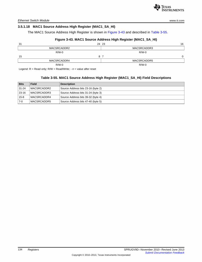
Ethernet Switch Module www.ti.com
134 SPRUGV9D–November 2010–Revised June 2013Submit Documentation Feedback
Copyright © 2010–2013, Texas Instruments Incorporated
Registers
3.5.1.18 MAC1 Source Address High Register (MAC1_SA_HI)The MAC1 Source Address High Register is shown in Figure 3-43 and described in Table 3-55.
Figure 3-43. MAC1 Source Address High Register (MAC1_SA_HI)31 24 23 16
MACSRCADDR2 MACSRCADDR3R/W-0 R/W-0
15 8 7 0MACSRCADDR4 MACSRCADDR5
R/W-0 R/W-0Legend: R = Read only; R/W = Read/Write; - n = value after reset
Table 3-55. MAC1 Source Address High Register (MAC1_SA_HI) Field Descriptions
Bits Field Description31-24 MACSRCADDR2 Source Address bits 23-16 (byte 2)23-16 MACSRCADDR3 Source Address bits 31-24 (byte 3)15-8 MACSRCADDR4 Source Address bits 39-32 (byte 4)7-0 MACSRCADDR5 Source Address bits 47-40 (byte 5)
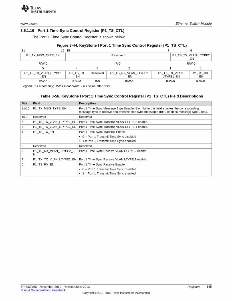
www.ti.com Ethernet Switch Module
135SPRUGV9D–November 2010–Revised June 2013Submit Documentation Feedback
Copyright © 2010–2013, Texas Instruments Incorporated
Registers
3.5.1.19 Port 1 Time Sync Control Register (P1_TS_CTL)The Port 1 Time Sync Control Register is shown below.
Figure 3-44. KeyStone I Port 1 Time Sync Control Register (P1_TS_CTL)31 16 15 7 6
P1_TX_MSG_TYPE_EN Reserved P1_TS_TX_VLAN_LTYPE2_EN
R/W-0 R-0 R/W-05 4 3 2 1 0
P1_TS_TX_VLAN_LTYPE1_EN
P1_TS_TX_EN
Reserved P1_TS_RX_VLAN_LTYPE2_EN
P1_TX_TX_VLAN_LTYPE1_EN
P1_TS_RX_EN
R/W-0 R/W-0 R-0 R/W-0 R/W-0 R/W-0Legend: R = Read only; R/W = Read/Write; - n = value after reset
Table 3-56. KeyStone I Port 1 Time Sync Control Register (P1_TS_CTL) Field Descriptions
Bits Field Description31-16 P1_TX_MSG_TYPE_EN Port 1 Time Sync Message Type Enable. Each bit in this field enables the corresponding
message type in receive and transmit time sync messages (Bit 0 enables message type 0 etc.).15-7 Reserved Reserved6 P1_TS_TX_VLAN_LTYPE2_EN Port 1 Time Sync Transmit VLAN LTYPE 2 enable.5 P1_TS_TX_VLAN_LTYPE1_EN Port 1 Time Sync Transmit VLAN LTYPE 1 enable.4 P1_TS_TX_EN Port 1 Time Sync Transmit Enable.
• 0 = Port 1 Transmit Time Sync disabled• 1 = Port 1 Transmit Time Sync enabled
3 Reserved Reserved2 P1_TS_RX_VLAN_LTYPE2_E
NPort 1 Time Sync Receive VLAN LTYPE 2 enable.
1 P1_TX_TX_VLAN_LTYPE1_EN Port 1 Time Sync Receive VLAN LTYPE 1 enable.0 P1_TS_RX_EN Port 1 Time Sync Receive Enable.
• 0 = Port 1 Transmit Time Sync disabled• 1 = Port 1 Transmit Time Sync enabled
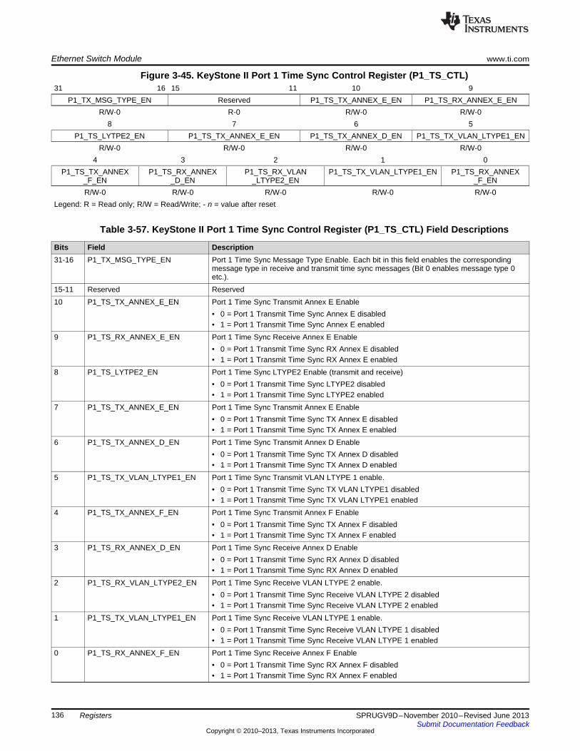
Ethernet Switch Module www.ti.com
136 SPRUGV9D–November 2010–Revised June 2013Submit Documentation Feedback
Copyright © 2010–2013, Texas Instruments Incorporated
Registers
Figure 3-45. KeyStone II Port 1 Time Sync Control Register (P1_TS_CTL)31 16 15 11 10 9
P1_TX_MSG_TYPE_EN Reserved P1_TS_TX_ANNEX_E_EN P1_TS_RX_ANNEX_E_ENR/W-0 R-0 R/W-0 R/W-0
8 7 6 5P1_TS_LYTPE2_EN P1_TS_TX_ANNEX_E_EN P1_TS_TX_ANNEX_D_EN P1_TS_TX_VLAN_LTYPE1_EN
R/W-0 R/W-0 R/W-0 R/W-04 3 2 1 0
P1_TS_TX_ANNEX_F_EN
P1_TS_RX_ANNEX_D_EN
P1_TS_RX_VLAN_LTYPE2_EN
P1_TS_TX_VLAN_LTYPE1_EN P1_TS_RX_ANNEX_F_EN
R/W-0 R/W-0 R/W-0 R/W-0 R/W-0Legend: R = Read only; R/W = Read/Write; - n = value after reset
Table 3-57. KeyStone II Port 1 Time Sync Control Register (P1_TS_CTL) Field Descriptions
Bits Field Description31-16 P1_TX_MSG_TYPE_EN Port 1 Time Sync Message Type Enable. Each bit in this field enables the corresponding
message type in receive and transmit time sync messages (Bit 0 enables message type 0etc.).
15-11 Reserved Reserved10 P1_TS_TX_ANNEX_E_EN Port 1 Time Sync Transmit Annex E Enable
• 0 = Port 1 Transmit Time Sync Annex E disabled• 1 = Port 1 Transmit Time Sync Annex E enabled
9 P1_TS_RX_ANNEX_E_EN Port 1 Time Sync Receive Annex E Enable• 0 = Port 1 Transmit Time Sync RX Annex E disabled• 1 = Port 1 Transmit Time Sync RX Annex E enabled
8 P1_TS_LYTPE2_EN Port 1 Time Sync LTYPE2 Enable (transmit and receive)• 0 = Port 1 Transmit Time Sync LTYPE2 disabled• 1 = Port 1 Transmit Time Sync LTYPE2 enabled
7 P1_TS_TX_ANNEX_E_EN Port 1 Time Sync Transmit Annex E Enable• 0 = Port 1 Transmit Time Sync TX Annex E disabled• 1 = Port 1 Transmit Time Sync TX Annex E enabled
6 P1_TS_TX_ANNEX_D_EN Port 1 Time Sync Transmit Annex D Enable• 0 = Port 1 Transmit Time Sync TX Annex D disabled• 1 = Port 1 Transmit Time Sync TX Annex D enabled
5 P1_TS_TX_VLAN_LTYPE1_EN Port 1 Time Sync Transmit VLAN LTYPE 1 enable.• 0 = Port 1 Transmit Time Sync TX VLAN LTYPE1 disabled• 1 = Port 1 Transmit Time Sync TX VLAN LTYPE1 enabled
4 P1_TS_TX_ANNEX_F_EN Port 1 Time Sync Transmit Annex F Enable• 0 = Port 1 Transmit Time Sync TX Annex F disabled• 1 = Port 1 Transmit Time Sync TX Annex F enabled
3 P1_TS_RX_ANNEX_D_EN Port 1 Time Sync Receive Annex D Enable• 0 = Port 1 Transmit Time Sync RX Annex D disabled• 1 = Port 1 Transmit Time Sync RX Annex D enabled
2 P1_TS_RX_VLAN_LTYPE2_EN Port 1 Time Sync Receive VLAN LTYPE 2 enable.• 0 = Port 1 Transmit Time Sync Receive VLAN LTYPE 2 disabled• 1 = Port 1 Transmit Time Sync Receive VLAN LTYPE 2 enabled
1 P1_TS_TX_VLAN_LTYPE1_EN Port 1 Time Sync Receive VLAN LTYPE 1 enable.• 0 = Port 1 Transmit Time Sync Receive VLAN LTYPE 1 disabled• 1 = Port 1 Transmit Time Sync Receive VLAN LTYPE 1 enabled
0 P1_TS_RX_ANNEX_F_EN Port 1 Time Sync Receive Annex F Enable• 0 = Port 1 Transmit Time Sync RX Annex F disabled• 1 = Port 1 Transmit Time Sync RX Annex F enabled

www.ti.com Ethernet Switch Module
137SPRUGV9D–November 2010–Revised June 2013Submit Documentation Feedback
Copyright © 2010–2013, Texas Instruments Incorporated
Registers
3.5.1.20 Port 1 Time Sync Sequence ID and LTYPE Register (P1_TS_SEQ_LTYPE)The Port 1 Time Sync Sequence ID and LTYPE Register is shown in Figure 3-46 and described inTable 3-58.
Figure 3-46. Port 1 Time Sync Sequence ID and LTYPE Register (P1_TS_SEQ_LTYPE)31 22 21 16 15 0
Reserved P1_TS_SEQ_ID_OFFSET
P1_TS_LTYPE
R-0 R/W-1Eh R/W-0Legend: R = Read only; R/W = Read/Write; - n = value after reset
Table 3-58. Port 1 Time Sync Sequence ID and LTYPE Register (P1_TS_SEQ_LTYPE) FieldDescriptions
Bits Field Description31-22 Reserved Reserved21-16 P1_TS_SEQ_ID_OFFSET Port 1 Time Sync Sequence ID Offset. This is the number of octets that the sequence ID is offset
in the transmit and receive time sync message header. The minimum value is 6.15-0 P1_TS_LTYPE Port 1 Time Sync LTYPE. This is the LTYPE value to match for transmit and receive time sync
messages.
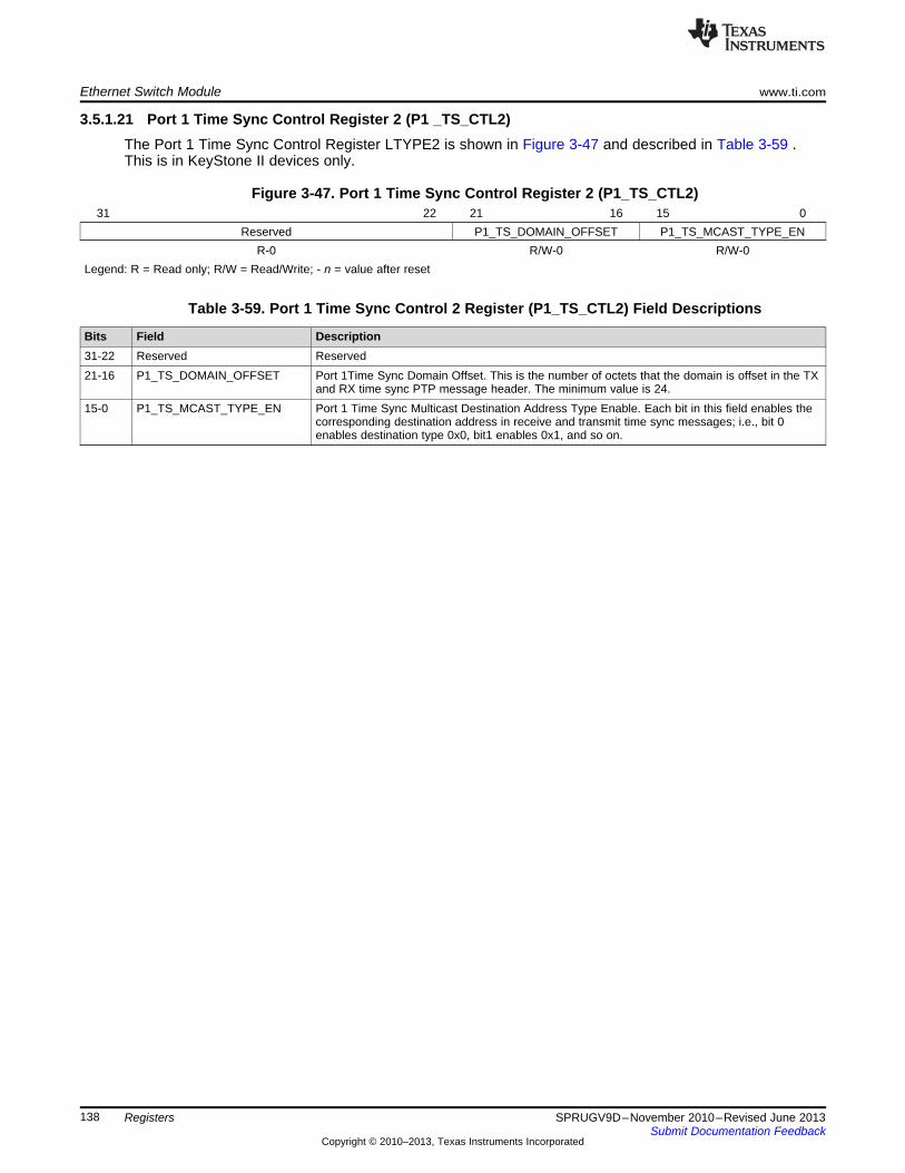
Ethernet Switch Module www.ti.com
138 SPRUGV9D–November 2010–Revised June 2013Submit Documentation Feedback
Copyright © 2010–2013, Texas Instruments Incorporated
Registers
3.5.1.21 Port 1 Time Sync Control Register 2 (P1 _TS_CTL2)The Port 1 Time Sync Control Register LTYPE2 is shown in Figure 3-47 and described in Table 3-59 .This is in KeyStone II devices only.
Figure 3-47. Port 1 Time Sync Control Register 2 (P1_TS_CTL2)31 22 21 16 15 0
Reserved P1_TS_DOMAIN_OFFSET P1_TS_MCAST_TYPE_ENR-0 R/W-0 R/W-0
Legend: R = Read only; R/W = Read/Write; - n = value after reset
Table 3-59. Port 1 Time Sync Control 2 Register (P1_TS_CTL2) Field Descriptions
Bits Field Description31-22 Reserved Reserved21-16 P1_TS_DOMAIN_OFFSET Port 1Time Sync Domain Offset. This is the number of octets that the domain is offset in the TX
and RX time sync PTP message header. The minimum value is 24.15-0 P1_TS_MCAST_TYPE_EN Port 1 Time Sync Multicast Destination Address Type Enable. Each bit in this field enables the
corresponding destination address in receive and transmit time sync messages; i.e., bit 0enables destination type 0x0, bit1 enables 0x1, and so on.
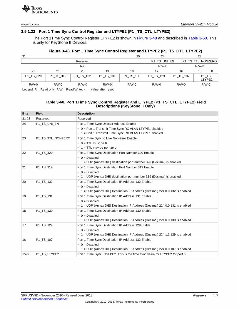
www.ti.com Ethernet Switch Module
139SPRUGV9D–November 2010–Revised June 2013Submit Documentation Feedback
Copyright © 2010–2013, Texas Instruments Incorporated
Registers
3.5.1.22 Port 1 Time Sync Control Register and LTYPE2 (P1 _TS_CTL_LTYPE2)The Port 1Time Sync Control Register LTYPE2 is shown in Figure 3-48 and described in Table 3-60. Thisis only for KeyStone II Devices.
Figure 3-48. Port 1 Time Sync Control Register and LTYPE2 (P1_TS_CTL_LTYPE2)31 25 24 23
Reserved P1_TS_UNI_EN P1_TS_TTL_NONZEROR-0 R/W-0 R/W-0
22 21 20 19 18 17 16 15 0P1_TS_320 P1_TS_319 P1_TS_132 P1_TS_131 P1_TS_130 P1_TS_129 P1_TS_107 P1_TS
_LTYPE2R/W-0 R/W-0 R/W-0 R/W-0 R/W-0 R/W-0 R/W-0 R/W-0
Legend: R = Read only; R/W = Read/Write; - n = value after reset
Table 3-60. Port 1Time Sync Control Register and LTYPE2 (P1_TS_CTL_LTYPE2) FieldDescriptions (KeyStone II Only)
Bits Field Description31-25 Reserved Reserved24 P1_TS_UNI_EN Port 1 Time Sync Unicast Address Enable
• 0 = Port 1 Transmit Time Sync RX VLAN LTYPE1 disabled• 1 = Port 1 Transmit Time Sync RX VLAN LTYPE1 enabled
23 P1_TS_TTL_NONZERO Port 1 Time Sync to Live Non-Zero Enable• 0 = TTL must be 0• 1 = TTL may be non-zero
22 P1_TS_320 Port 1 Time Sync Destination Port Number 320 Enable• 0 = Disabled• 1 = UDP (Annex D/E) destination port number 320 (Decimal) is enabled.
21 P1_TS_319 Port 1 Time Sync Destination Port Number 319 Enable• 0 = Disabled• 1 = UDP (Annex D/E) destination port number 319 (Decimal) is enabled.
20 P1_TS_132 Port 1 Time Sync Destination IP Address 132 Enable• 0 = Disabled• 1 = UDP (Annex D/E) Destination IP Address (Decimal) 224.0.0.132 is enabled
19 P1_TS_131 Port 1 Time Sync Destination IP Address 131 Enable• 0 = Disabled• 1 = UDP (Annex D/E) Destination IP Address (Decimal) 224.0.0.131 is enabled
18 P1_TS_130 Port 1 Time Sync Destination IP Address 130 Enable• 0 = Disabled• 1 = UDP (Annex D/E) Destination IP Address (Decimal) 224.0.0.130 is enabled
17 P1_TS_129 Port 1 Time Sync Destination IP Address 129Enable• 0 = Disabled• 1 = UDP (Annex D/E) Destination IP Address (Decimal) 224.1.1.129 is enabled
16 P1_TS_107 Port 1 Time Sync Destination IP Address 132 Enable• 0 = Disabled• 1 = UDP (Annex D/E) Destination IP Address (Decimal) 224.0.0.107 is enabled
15-0 P1_TS_LTYPE2 Port 1 Time Sync LTYLPE2. This is the time sync value for LTYPE2 for port 3.
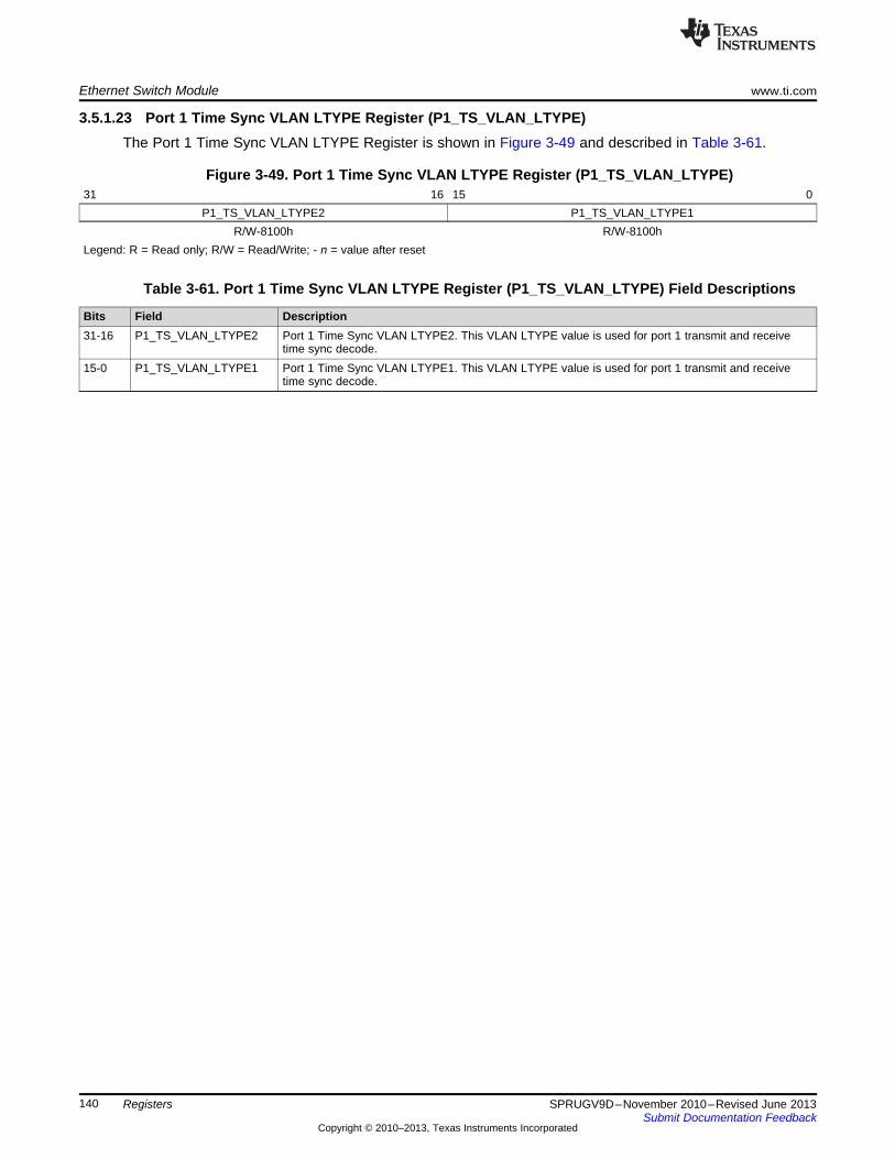
Ethernet Switch Module www.ti.com
140 SPRUGV9D–November 2010–Revised June 2013Submit Documentation Feedback
Copyright © 2010–2013, Texas Instruments Incorporated
Registers
3.5.1.23 Port 1 Time Sync VLAN LTYPE Register (P1_TS_VLAN_LTYPE)The Port 1 Time Sync VLAN LTYPE Register is shown in Figure 3-49 and described in Table 3-61.
Figure 3-49. Port 1 Time Sync VLAN LTYPE Register (P1_TS_VLAN_LTYPE)31 16 15 0
P1_TS_VLAN_LTYPE2 P1_TS_VLAN_LTYPE1R/W-8100h R/W-8100h
Legend: R = Read only; R/W = Read/Write; - n = value after reset
Table 3-61. Port 1 Time Sync VLAN LTYPE Register (P1_TS_VLAN_LTYPE) Field Descriptions
Bits Field Description31-16 P1_TS_VLAN_LTYPE2 Port 1 Time Sync VLAN LTYPE2. This VLAN LTYPE value is used for port 1 transmit and receive
time sync decode.15-0 P1_TS_VLAN_LTYPE1 Port 1 Time Sync VLAN LTYPE1. This VLAN LTYPE value is used for port 1 transmit and receive
time sync decode.
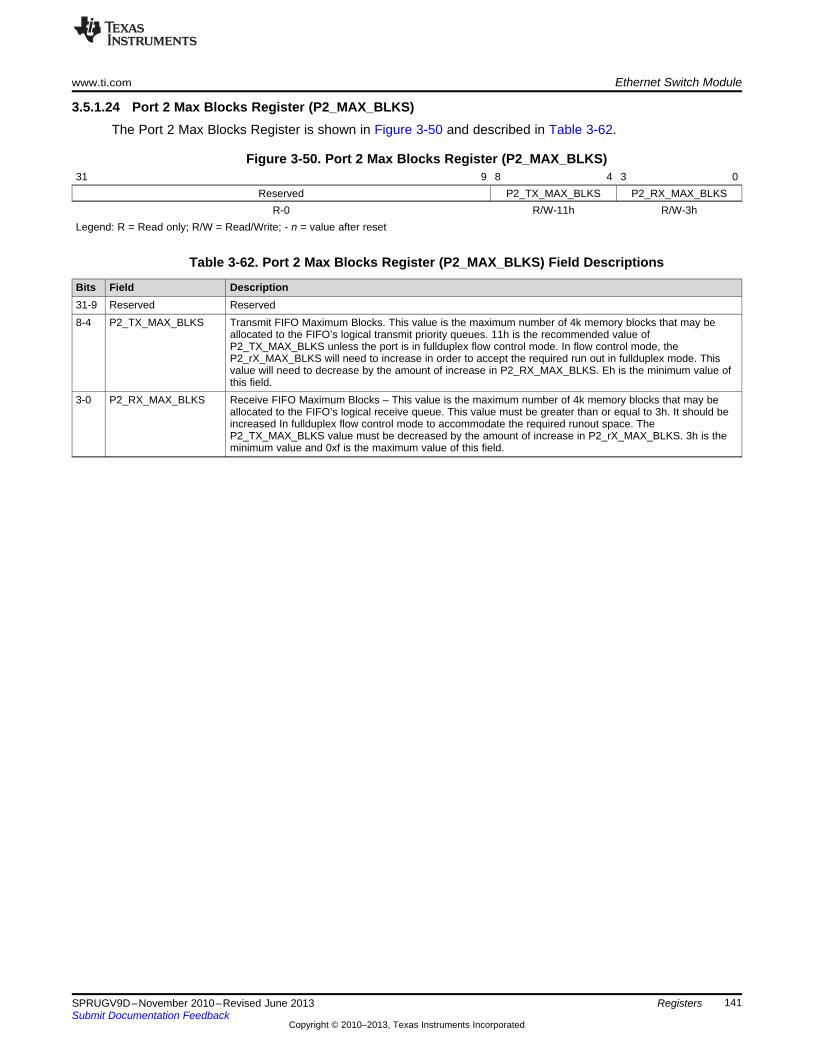
www.ti.com Ethernet Switch Module
141SPRUGV9D–November 2010–Revised June 2013Submit Documentation Feedback
Copyright © 2010–2013, Texas Instruments Incorporated
Registers
3.5.1.24 Port 2 Max Blocks Register (P2_MAX_BLKS)The Port 2 Max Blocks Register is shown in Figure 3-50 and described in Table 3-62.
Figure 3-50. Port 2 Max Blocks Register (P2_MAX_BLKS)31 9 8 4 3 0
Reserved P2_TX_MAX_BLKS P2_RX_MAX_BLKSR-0 R/W-11h R/W-3h
Legend: R = Read only; R/W = Read/Write; - n = value after reset
Table 3-62. Port 2 Max Blocks Register (P2_MAX_BLKS) Field Descriptions
Bits Field Description31-9 Reserved Reserved8-4 P2_TX_MAX_BLKS Transmit FIFO Maximum Blocks. This value is the maximum number of 4k memory blocks that may be
allocated to the FIFO’s logical transmit priority queues. 11h is the recommended value ofP2_TX_MAX_BLKS unless the port is in fullduplex flow control mode. In flow control mode, theP2_rX_MAX_BLKS will need to increase in order to accept the required run out in fullduplex mode. Thisvalue will need to decrease by the amount of increase in P2_RX_MAX_BLKS. Eh is the minimum value ofthis field.
3-0 P2_RX_MAX_BLKS Receive FIFO Maximum Blocks – This value is the maximum number of 4k memory blocks that may beallocated to the FIFO’s logical receive queue. This value must be greater than or equal to 3h. It should beincreased In fullduplex flow control mode to accommodate the required runout space. TheP2_TX_MAX_BLKS value must be decreased by the amount of increase in P2_rX_MAX_BLKS. 3h is theminimum value and 0xf is the maximum value of this field.
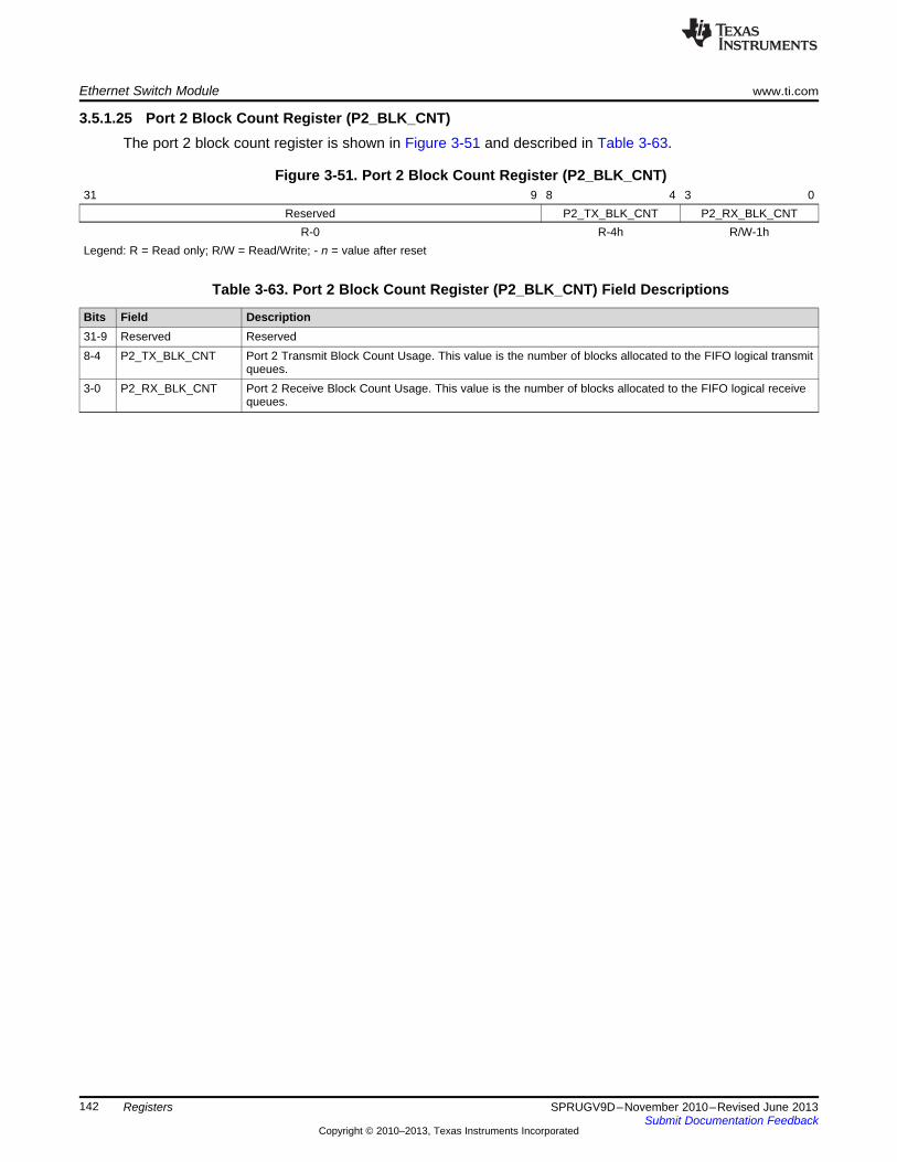
Ethernet Switch Module www.ti.com
142 SPRUGV9D–November 2010–Revised June 2013Submit Documentation Feedback
Copyright © 2010–2013, Texas Instruments Incorporated
Registers
3.5.1.25 Port 2 Block Count Register (P2_BLK_CNT)The port 2 block count register is shown in Figure 3-51 and described in Table 3-63.
Figure 3-51. Port 2 Block Count Register (P2_BLK_CNT)31 9 8 4 3 0
Reserved P2_TX_BLK_CNT P2_RX_BLK_CNTR-0 R-4h R/W-1h
Legend: R = Read only; R/W = Read/Write; - n = value after reset
Table 3-63. Port 2 Block Count Register (P2_BLK_CNT) Field Descriptions
Bits Field Description31-9 Reserved Reserved8-4 P2_TX_BLK_CNT Port 2 Transmit Block Count Usage. This value is the number of blocks allocated to the FIFO logical transmit
queues.3-0 P2_RX_BLK_CNT Port 2 Receive Block Count Usage. This value is the number of blocks allocated to the FIFO logical receive
queues.
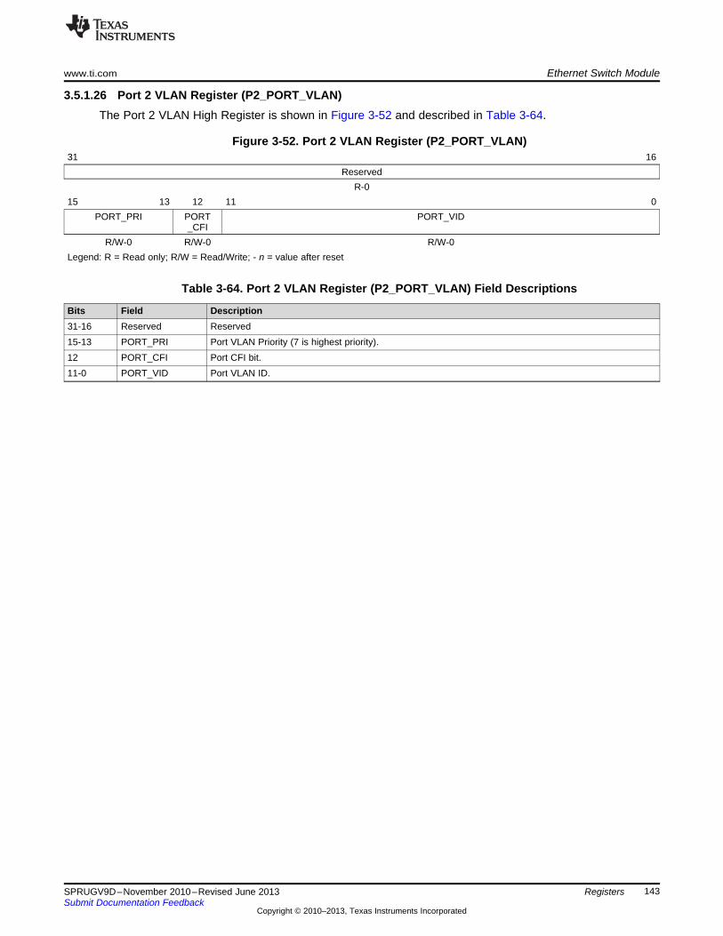
www.ti.com Ethernet Switch Module
143SPRUGV9D–November 2010–Revised June 2013Submit Documentation Feedback
Copyright © 2010–2013, Texas Instruments Incorporated
Registers
3.5.1.26 Port 2 VLAN Register (P2_PORT_VLAN)The Port 2 VLAN High Register is shown in Figure 3-52 and described in Table 3-64.
Figure 3-52. Port 2 VLAN Register (P2_PORT_VLAN)31 16
ReservedR-0
15 13 12 11 0PORT_PRI PORT
_CFIPORT_VID
R/W-0 R/W-0 R/W-0Legend: R = Read only; R/W = Read/Write; - n = value after reset
Table 3-64. Port 2 VLAN Register (P2_PORT_VLAN) Field Descriptions
Bits Field Description31-16 Reserved Reserved15-13 PORT_PRI Port VLAN Priority (7 is highest priority).12 PORT_CFI Port CFI bit.11-0 PORT_VID Port VLAN ID.
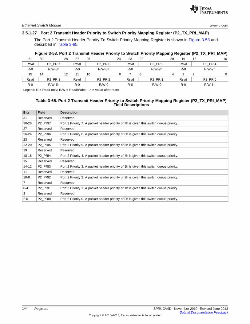
Ethernet Switch Module www.ti.com
144 SPRUGV9D–November 2010–Revised June 2013Submit Documentation Feedback
Copyright © 2010–2013, Texas Instruments Incorporated
Registers
3.5.1.27 Port 2 Transmit Header Priority to Switch Priority Mapping Register (P2_TX_PRI_MAP)The Port 2 Transmit Header Priority To Switch Priority Mapping Register is shown in Figure 3-53 anddescribed in Table 3-65.
Figure 3-53. Port 2 Transmit Header Priority to Switch Priority Mapping Register (P2_TX_PRI_MAP)31 30 28 27 26 24 23 22 20 19 18 16
Rsvd P2_PRI7 Rsvd P2_PRI6 Rsvd P2_PRI5 Rsvd P2_PRI4R-0 R/W-3h R-0 R/W-3h R-0 R/W-2h R-0 R/W-2h15 14 12 11 10 8 7 6 4 3 2 0
Rsvd P2_PRI3 Rsvd P2_PRI2 Rsvd P2_PRI1 Rsvd P2_PRI0R-0 R/W-1h R-0 R/W-0 R-0 R/W-0 R-0 R/W-1h
Legend: R = Read only; R/W = Read/Write; - n = value after reset
Table 3-65. Port 2 Transmit Header Priority to Switch Priority Mapping Register (P2_TX_PRI_MAP)Field Descriptions
Bits Field Description31 Reserved Reserved30-28 P2_PRI7 Port 2 Priority 7. A packet header priority of 7h is given this switch queue priority.27 Reserved Reserved26-24 P2_PRI6 Port 2 Priority 6. A packet header priority of 6h is given this switch queue priority.23 Reserved Reserved22-20 P2_PRI5 Port 2 Priority 5. A packet header priority of 5h is given this switch queue priority.19 Reserved Reserved18-16 P2_PRI4 Port 2 Priority 4. A packet header priority of 4h is given this switch queue priority.15 Reserved Reserved14-12 P2_PRI3 Port 2 Priority 3. A packet header priority of 3h is given this switch queue priority.11 Reserved Reserved10-8 P2_PRI2 Port 2 Priority 2. A packet header priority of 2h is given this switch queue priority.7 Reserved Reserved6-4 P2_PRI1 Port 2 Priority 1. A packet header priority of 1h is given this switch queue priority.3 Reserved Reserved2-0 P2_PRI0 Port 2 Priority 0. A packet header priority of 0h is given this switch queue priority.

www.ti.com Ethernet Switch Module
145SPRUGV9D–November 2010–Revised June 2013Submit Documentation Feedback
Copyright © 2010–2013, Texas Instruments Incorporated
Registers
3.5.1.28 MAC2 Source Address Low Register (MAC2_SA_LO)The MAC2 Source Address Low Register is shown in Figure 3-54 and described in Table 3-66.
Figure 3-54. MAC2 Source Address Low Register (MAC2_SA_LO)31 16
ReservedR-0
15 8 7 0MACSRCADDR0 MACSRCADDR1
R/W-0 R/W-0Legend: R = Read only; R/W = Read/Write; - n = value after reset
Table 3-66. MAC2 Source Address Low Register (MAC2_SA_LO) Field Descriptions
Bits Field Description31-16 Reserved Reserved15-8 MACSRCADDR0 Source address bits 7-0 (byte 0).7-0 MACSRCADDR1 Source address bits 15-8 (byte 1).
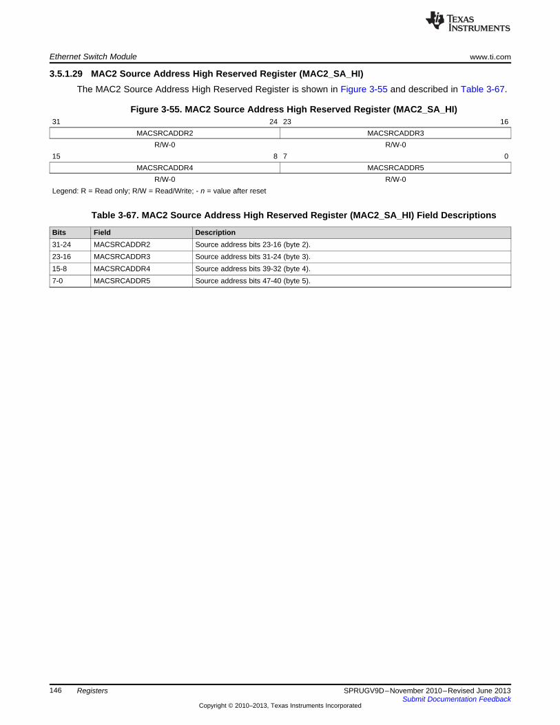
Ethernet Switch Module www.ti.com
146 SPRUGV9D–November 2010–Revised June 2013Submit Documentation Feedback
Copyright © 2010–2013, Texas Instruments Incorporated
Registers
3.5.1.29 MAC2 Source Address High Reserved Register (MAC2_SA_HI)The MAC2 Source Address High Reserved Register is shown in Figure 3-55 and described in Table 3-67.
Figure 3-55. MAC2 Source Address High Reserved Register (MAC2_SA_HI)31 24 23 16
MACSRCADDR2 MACSRCADDR3R/W-0 R/W-0
15 8 7 0MACSRCADDR4 MACSRCADDR5
R/W-0 R/W-0Legend: R = Read only; R/W = Read/Write; - n = value after reset
Table 3-67. MAC2 Source Address High Reserved Register (MAC2_SA_HI) Field Descriptions
Bits Field Description31-24 MACSRCADDR2 Source address bits 23-16 (byte 2).23-16 MACSRCADDR3 Source address bits 31-24 (byte 3).15-8 MACSRCADDR4 Source address bits 39-32 (byte 4).7-0 MACSRCADDR5 Source address bits 47-40 (byte 5).
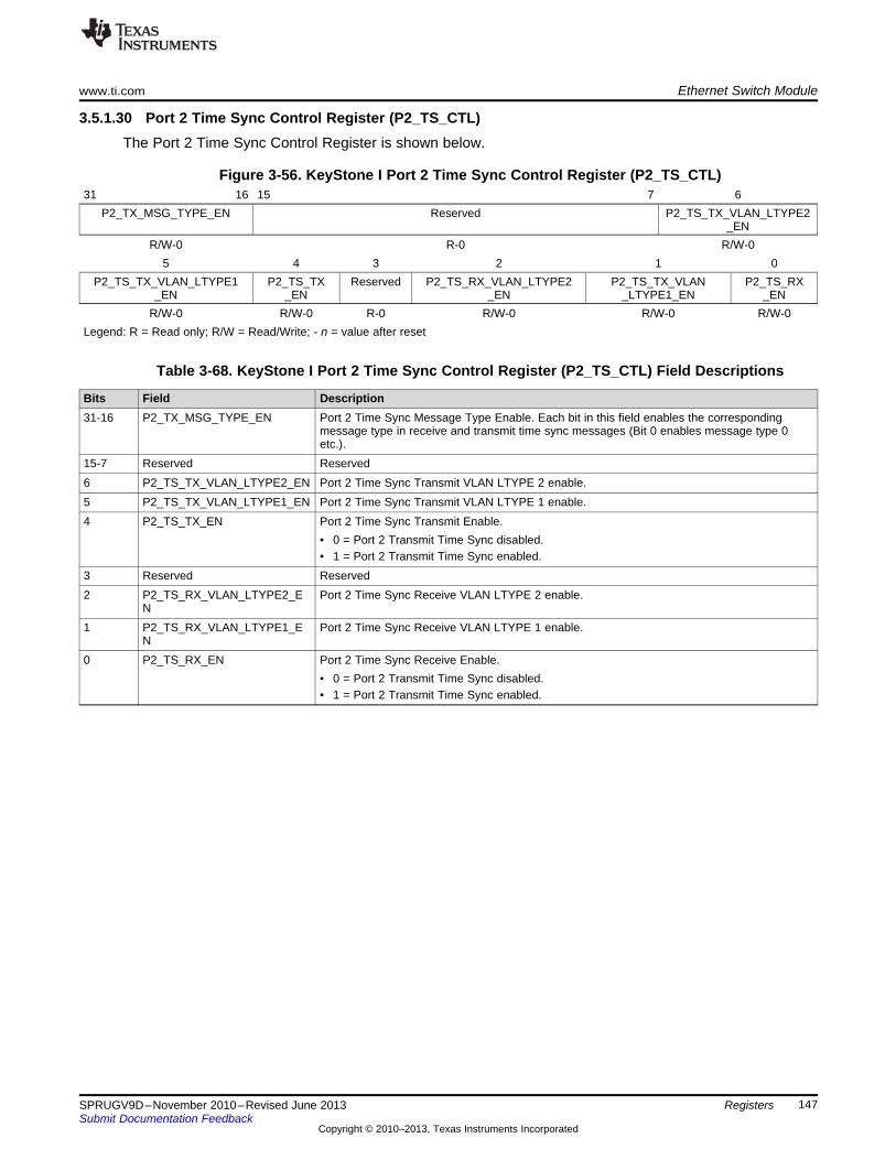
www.ti.com Ethernet Switch Module
147SPRUGV9D–November 2010–Revised June 2013Submit Documentation Feedback
Copyright © 2010–2013, Texas Instruments Incorporated
Registers
3.5.1.30 Port 2 Time Sync Control Register (P2_TS_CTL)The Port 2 Time Sync Control Register is shown below.
Figure 3-56. KeyStone I Port 2 Time Sync Control Register (P2_TS_CTL)31 16 15 7 6
P2_TX_MSG_TYPE_EN Reserved P2_TS_TX_VLAN_LTYPE2_EN
R/W-0 R-0 R/W-05 4 3 2 1 0
P2_TS_TX_VLAN_LTYPE1_EN
P2_TS_TX_EN
Reserved P2_TS_RX_VLAN_LTYPE2_EN
P2_TS_TX_VLAN_LTYPE1_EN
P2_TS_RX_EN
R/W-0 R/W-0 R-0 R/W-0 R/W-0 R/W-0Legend: R = Read only; R/W = Read/Write; - n = value after reset
Table 3-68. KeyStone I Port 2 Time Sync Control Register (P2_TS_CTL) Field Descriptions
Bits Field Description31-16 P2_TX_MSG_TYPE_EN Port 2 Time Sync Message Type Enable. Each bit in this field enables the corresponding
message type in receive and transmit time sync messages (Bit 0 enables message type 0etc.).
15-7 Reserved Reserved6 P2_TS_TX_VLAN_LTYPE2_EN Port 2 Time Sync Transmit VLAN LTYPE 2 enable.5 P2_TS_TX_VLAN_LTYPE1_EN Port 2 Time Sync Transmit VLAN LTYPE 1 enable.4 P2_TS_TX_EN Port 2 Time Sync Transmit Enable.
• 0 = Port 2 Transmit Time Sync disabled.• 1 = Port 2 Transmit Time Sync enabled.
3 Reserved Reserved2 P2_TS_RX_VLAN_LTYPE2_E
NPort 2 Time Sync Receive VLAN LTYPE 2 enable.
1 P2_TS_RX_VLAN_LTYPE1_EN
Port 2 Time Sync Receive VLAN LTYPE 1 enable.
0 P2_TS_RX_EN Port 2 Time Sync Receive Enable.• 0 = Port 2 Transmit Time Sync disabled.• 1 = Port 2 Transmit Time Sync enabled.
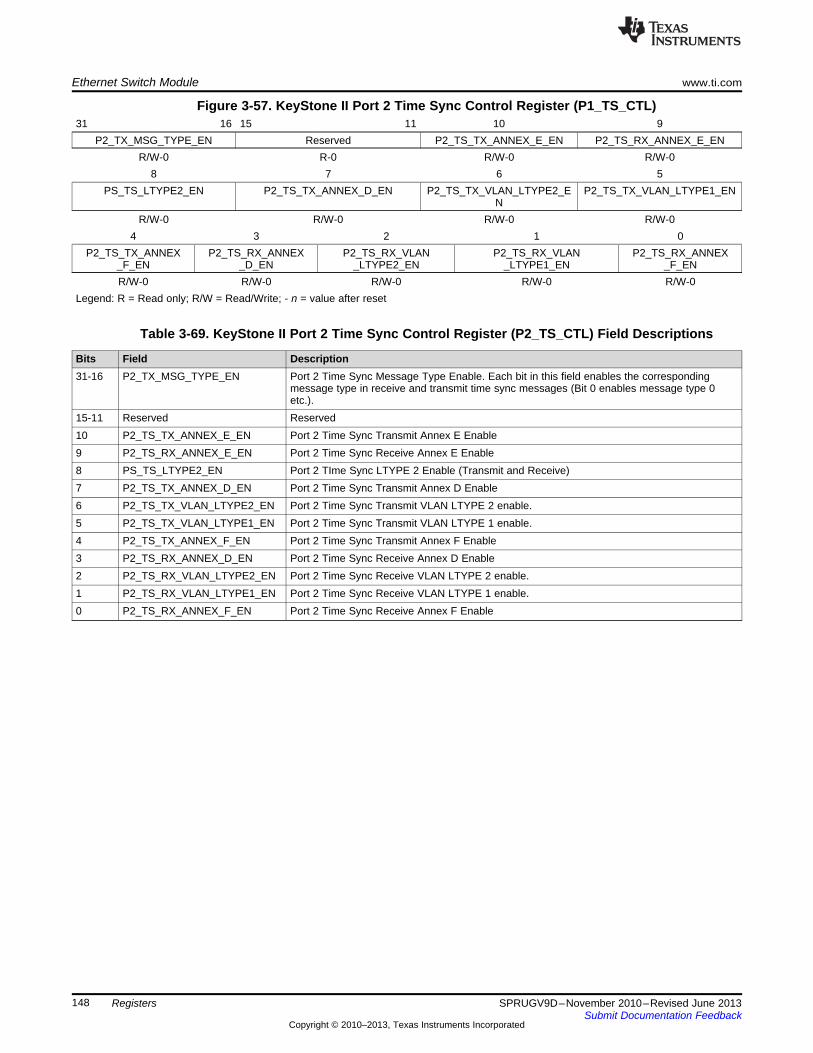
Ethernet Switch Module www.ti.com
148 SPRUGV9D–November 2010–Revised June 2013Submit Documentation Feedback
Copyright © 2010–2013, Texas Instruments Incorporated
Registers
Figure 3-57. KeyStone II Port 2 Time Sync Control Register (P1_TS_CTL)31 16 15 11 10 9
P2_TX_MSG_TYPE_EN Reserved P2_TS_TX_ANNEX_E_EN P2_TS_RX_ANNEX_E_ENR/W-0 R-0 R/W-0 R/W-0
8 7 6 5PS_TS_LTYPE2_EN P2_TS_TX_ANNEX_D_EN P2_TS_TX_VLAN_LTYPE2_E
NP2_TS_TX_VLAN_LTYPE1_EN
R/W-0 R/W-0 R/W-0 R/W-04 3 2 1 0
P2_TS_TX_ANNEX_F_EN
P2_TS_RX_ANNEX_D_EN
P2_TS_RX_VLAN_LTYPE2_EN
P2_TS_RX_VLAN_LTYPE1_EN
P2_TS_RX_ANNEX_F_EN
R/W-0 R/W-0 R/W-0 R/W-0 R/W-0Legend: R = Read only; R/W = Read/Write; - n = value after reset
Table 3-69. KeyStone II Port 2 Time Sync Control Register (P2_TS_CTL) Field Descriptions
Bits Field Description31-16 P2_TX_MSG_TYPE_EN Port 2 Time Sync Message Type Enable. Each bit in this field enables the corresponding
message type in receive and transmit time sync messages (Bit 0 enables message type 0etc.).
15-11 Reserved Reserved10 P2_TS_TX_ANNEX_E_EN Port 2 Time Sync Transmit Annex E Enable9 P2_TS_RX_ANNEX_E_EN Port 2 Time Sync Receive Annex E Enable8 PS_TS_LTYPE2_EN Port 2 TIme Sync LTYPE 2 Enable (Transmit and Receive)7 P2_TS_TX_ANNEX_D_EN Port 2 Time Sync Transmit Annex D Enable6 P2_TS_TX_VLAN_LTYPE2_EN Port 2 Time Sync Transmit VLAN LTYPE 2 enable.5 P2_TS_TX_VLAN_LTYPE1_EN Port 2 Time Sync Transmit VLAN LTYPE 1 enable.4 P2_TS_TX_ANNEX_F_EN Port 2 Time Sync Transmit Annex F Enable3 P2_TS_RX_ANNEX_D_EN Port 2 Time Sync Receive Annex D Enable2 P2_TS_RX_VLAN_LTYPE2_EN Port 2 Time Sync Receive VLAN LTYPE 2 enable.1 P2_TS_RX_VLAN_LTYPE1_EN Port 2 Time Sync Receive VLAN LTYPE 1 enable.0 P2_TS_RX_ANNEX_F_EN Port 2 Time Sync Receive Annex F Enable
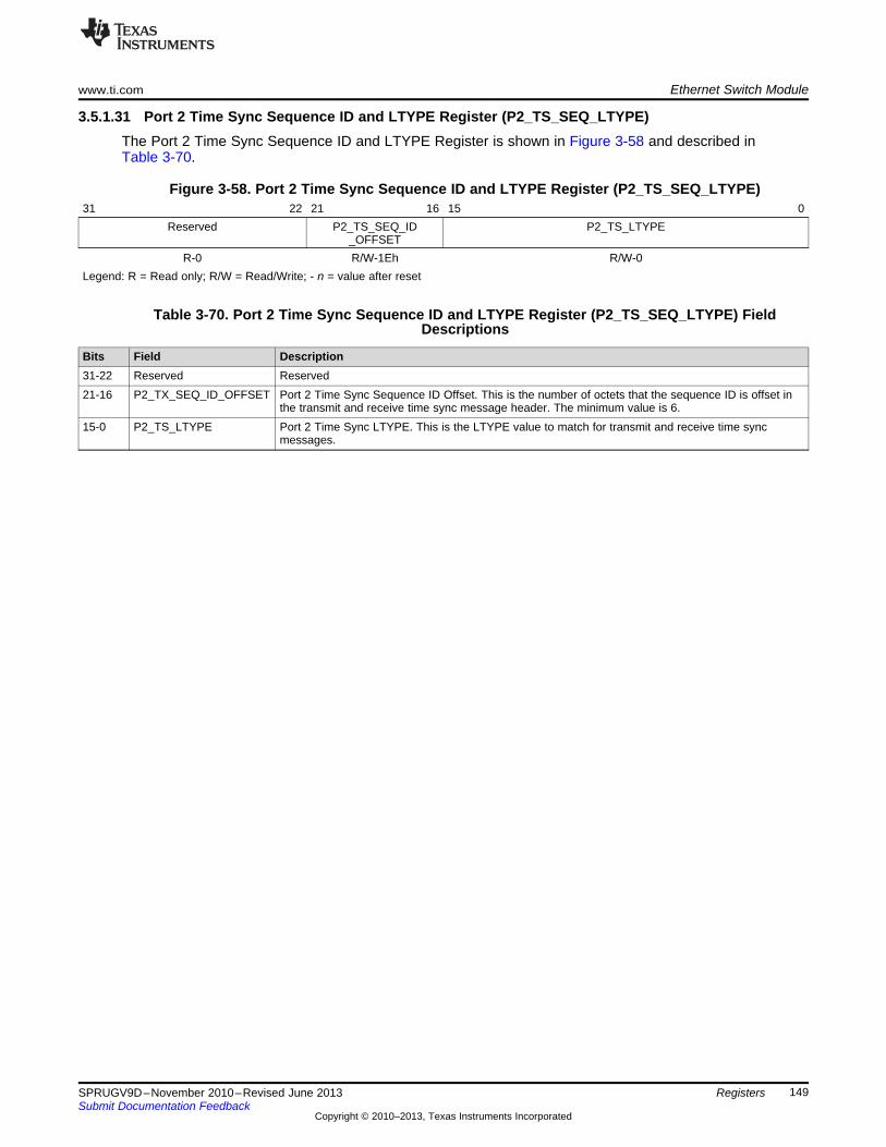
www.ti.com Ethernet Switch Module
149SPRUGV9D–November 2010–Revised June 2013Submit Documentation Feedback
Copyright © 2010–2013, Texas Instruments Incorporated
Registers
3.5.1.31 Port 2 Time Sync Sequence ID and LTYPE Register (P2_TS_SEQ_LTYPE)The Port 2 Time Sync Sequence ID and LTYPE Register is shown in Figure 3-58 and described inTable 3-70.
Figure 3-58. Port 2 Time Sync Sequence ID and LTYPE Register (P2_TS_SEQ_LTYPE)31 22 21 16 15 0
Reserved P2_TS_SEQ_ID_OFFSET
P2_TS_LTYPE
R-0 R/W-1Eh R/W-0Legend: R = Read only; R/W = Read/Write; - n = value after reset
Table 3-70. Port 2 Time Sync Sequence ID and LTYPE Register (P2_TS_SEQ_LTYPE) FieldDescriptions
Bits Field Description31-22 Reserved Reserved21-16 P2_TX_SEQ_ID_OFFSET Port 2 Time Sync Sequence ID Offset. This is the number of octets that the sequence ID is offset in
the transmit and receive time sync message header. The minimum value is 6.15-0 P2_TS_LTYPE Port 2 Time Sync LTYPE. This is the LTYPE value to match for transmit and receive time sync
messages.
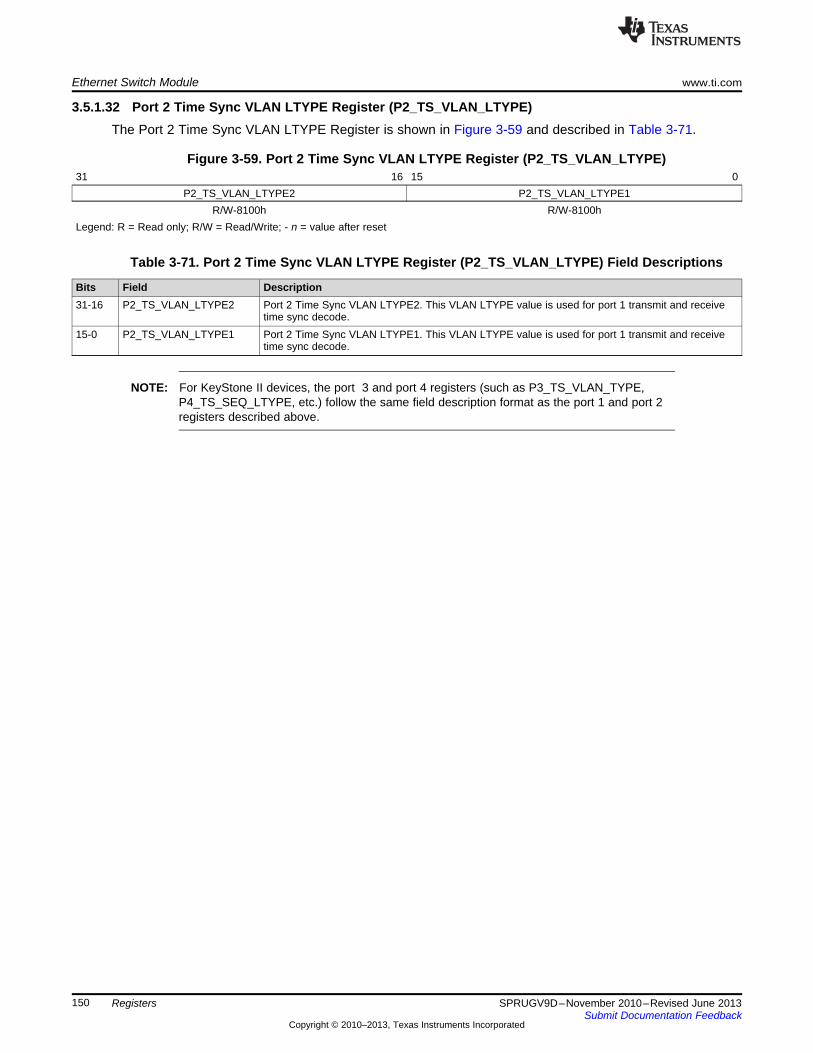
Ethernet Switch Module www.ti.com
150 SPRUGV9D–November 2010–Revised June 2013Submit Documentation Feedback
Copyright © 2010–2013, Texas Instruments Incorporated
Registers
3.5.1.32 Port 2 Time Sync VLAN LTYPE Register (P2_TS_VLAN_LTYPE)The Port 2 Time Sync VLAN LTYPE Register is shown in Figure 3-59 and described in Table 3-71.
Figure 3-59. Port 2 Time Sync VLAN LTYPE Register (P2_TS_VLAN_LTYPE)31 16 15 0
P2_TS_VLAN_LTYPE2 P2_TS_VLAN_LTYPE1R/W-8100h R/W-8100h
Legend: R = Read only; R/W = Read/Write; - n = value after reset
Table 3-71. Port 2 Time Sync VLAN LTYPE Register (P2_TS_VLAN_LTYPE) Field Descriptions
Bits Field Description31-16 P2_TS_VLAN_LTYPE2 Port 2 Time Sync VLAN LTYPE2. This VLAN LTYPE value is used for port 1 transmit and receive
time sync decode.15-0 P2_TS_VLAN_LTYPE1 Port 2 Time Sync VLAN LTYPE1. This VLAN LTYPE value is used for port 1 transmit and receive
time sync decode.
NOTE: For KeyStone II devices, the port 3 and port 4 registers (such as P3_TS_VLAN_TYPE,P4_TS_SEQ_LTYPE, etc.) follow the same field description format as the port 1 and port 2registers described above.
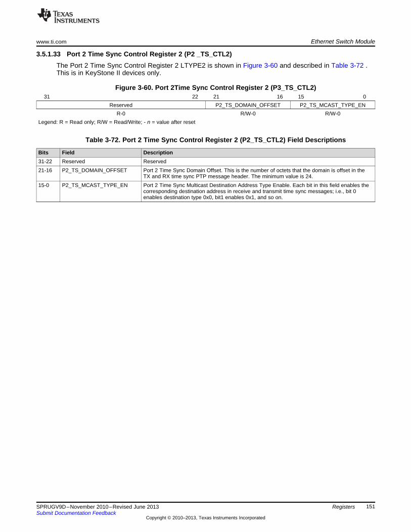
www.ti.com Ethernet Switch Module
151SPRUGV9D–November 2010–Revised June 2013Submit Documentation Feedback
Copyright © 2010–2013, Texas Instruments Incorporated
Registers
3.5.1.33 Port 2 Time Sync Control Register 2 (P2 _TS_CTL2)The Port 2 Time Sync Control Register 2 LTYPE2 is shown in Figure 3-60 and described in Table 3-72 .This is in KeyStone II devices only.
Figure 3-60. Port 2Time Sync Control Register 2 (P3_TS_CTL2)31 22 21 16 15 0
Reserved P2_TS_DOMAIN_OFFSET P2_TS_MCAST_TYPE_ENR-0 R/W-0 R/W-0
Legend: R = Read only; R/W = Read/Write; - n = value after reset
Table 3-72. Port 2 Time Sync Control Register 2 (P2_TS_CTL2) Field Descriptions
Bits Field Description31-22 Reserved Reserved21-16 P2_TS_DOMAIN_OFFSET Port 2 Time Sync Domain Offset. This is the number of octets that the domain is offset in the
TX and RX time sync PTP message header. The minimum value is 24.15-0 P2_TS_MCAST_TYPE_EN Port 2 Time Sync Multicast Destination Address Type Enable. Each bit in this field enables the
corresponding destination address in receive and transmit time sync messages; i.e., bit 0enables destination type 0x0, bit1 enables 0x1, and so on.
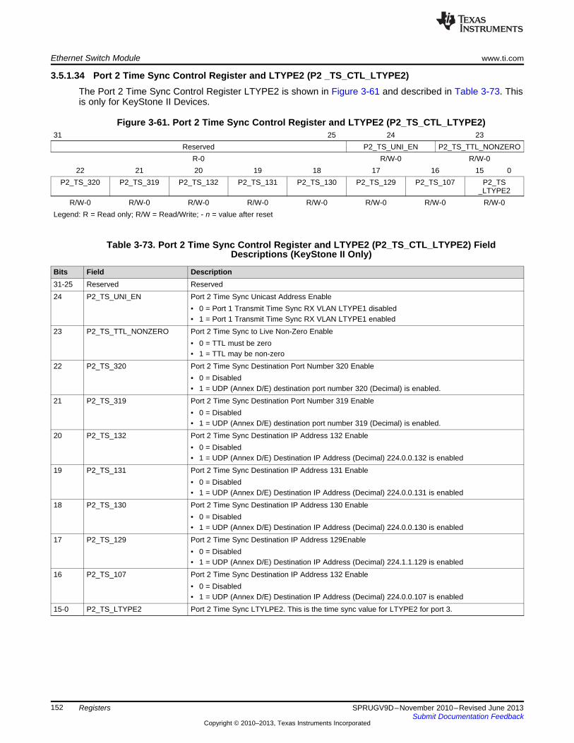
Ethernet Switch Module www.ti.com
152 SPRUGV9D–November 2010–Revised June 2013Submit Documentation Feedback
Copyright © 2010–2013, Texas Instruments Incorporated
Registers
3.5.1.34 Port 2 Time Sync Control Register and LTYPE2 (P2 _TS_CTL_LTYPE2)The Port 2 Time Sync Control Register LTYPE2 is shown in Figure 3-61 and described in Table 3-73. Thisis only for KeyStone II Devices.
Figure 3-61. Port 2 Time Sync Control Register and LTYPE2 (P2_TS_CTL_LTYPE2)31 25 24 23
Reserved P2_TS_UNI_EN P2_TS_TTL_NONZEROR-0 R/W-0 R/W-0
22 21 20 19 18 17 16 15 0P2_TS_320 P2_TS_319 P2_TS_132 P2_TS_131 P2_TS_130 P2_TS_129 P2_TS_107 P2_TS
_LTYPE2R/W-0 R/W-0 R/W-0 R/W-0 R/W-0 R/W-0 R/W-0 R/W-0
Legend: R = Read only; R/W = Read/Write; - n = value after reset
Table 3-73. Port 2 Time Sync Control Register and LTYPE2 (P2_TS_CTL_LTYPE2) FieldDescriptions (KeyStone II Only)
Bits Field Description31-25 Reserved Reserved24 P2_TS_UNI_EN Port 2 Time Sync Unicast Address Enable
• 0 = Port 1 Transmit Time Sync RX VLAN LTYPE1 disabled• 1 = Port 1 Transmit Time Sync RX VLAN LTYPE1 enabled
23 P2_TS_TTL_NONZERO Port 2 Time Sync to Live Non-Zero Enable• 0 = TTL must be zero• 1 = TTL may be non-zero
22 P2_TS_320 Port 2 Time Sync Destination Port Number 320 Enable• 0 = Disabled• 1 = UDP (Annex D/E) destination port number 320 (Decimal) is enabled.
21 P2_TS_319 Port 2 Time Sync Destination Port Number 319 Enable• 0 = Disabled• 1 = UDP (Annex D/E) destination port number 319 (Decimal) is enabled.
20 P2_TS_132 Port 2 Time Sync Destination IP Address 132 Enable• 0 = Disabled• 1 = UDP (Annex D/E) Destination IP Address (Decimal) 224.0.0.132 is enabled
19 P2_TS_131 Port 2 Time Sync Destination IP Address 131 Enable• 0 = Disabled• 1 = UDP (Annex D/E) Destination IP Address (Decimal) 224.0.0.131 is enabled
18 P2_TS_130 Port 2 Time Sync Destination IP Address 130 Enable• 0 = Disabled• 1 = UDP (Annex D/E) Destination IP Address (Decimal) 224.0.0.130 is enabled
17 P2_TS_129 Port 2 Time Sync Destination IP Address 129Enable• 0 = Disabled• 1 = UDP (Annex D/E) Destination IP Address (Decimal) 224.1.1.129 is enabled
16 P2_TS_107 Port 2 Time Sync Destination IP Address 132 Enable• 0 = Disabled• 1 = UDP (Annex D/E) Destination IP Address (Decimal) 224.0.0.107 is enabled
15-0 P2_TS_LTYPE2 Port 2 Time Sync LTYLPE2. This is the time sync value for LTYPE2 for port 3.
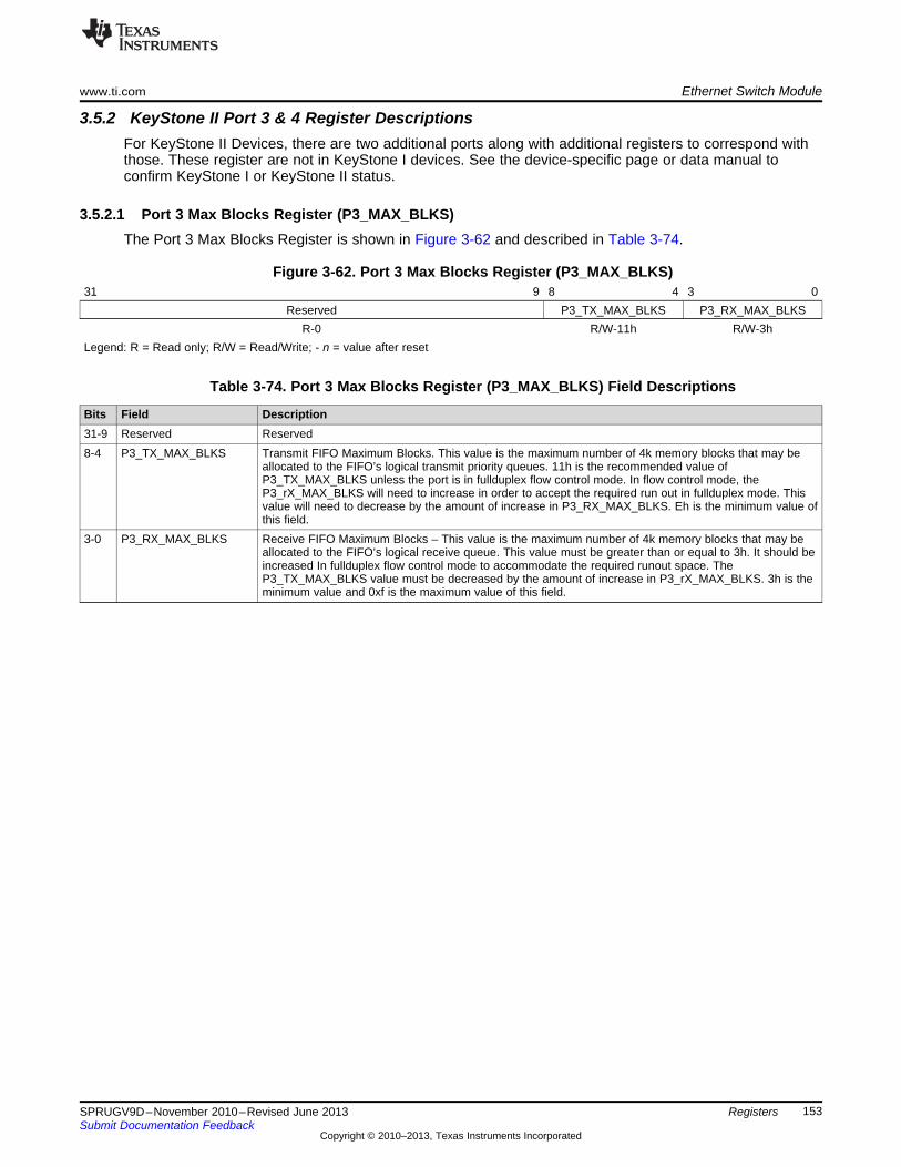
www.ti.com Ethernet Switch Module
153SPRUGV9D–November 2010–Revised June 2013Submit Documentation Feedback
Copyright © 2010–2013, Texas Instruments Incorporated
Registers
3.5.2 KeyStone II Port 3 & 4 Register DescriptionsFor KeyStone II Devices, there are two additional ports along with additional registers to correspond withthose. These register are not in KeyStone I devices. See the device-specific page or data manual toconfirm KeyStone I or KeyStone II status.
3.5.2.1 Port 3 Max Blocks Register (P3_MAX_BLKS)The Port 3 Max Blocks Register is shown in Figure 3-62 and described in Table 3-74.
Figure 3-62. Port 3 Max Blocks Register (P3_MAX_BLKS)31 9 8 4 3 0
Reserved P3_TX_MAX_BLKS P3_RX_MAX_BLKSR-0 R/W-11h R/W-3h
Legend: R = Read only; R/W = Read/Write; - n = value after reset
Table 3-74. Port 3 Max Blocks Register (P3_MAX_BLKS) Field Descriptions
Bits Field Description31-9 Reserved Reserved8-4 P3_TX_MAX_BLKS Transmit FIFO Maximum Blocks. This value is the maximum number of 4k memory blocks that may be
allocated to the FIFO’s logical transmit priority queues. 11h is the recommended value ofP3_TX_MAX_BLKS unless the port is in fullduplex flow control mode. In flow control mode, theP3_rX_MAX_BLKS will need to increase in order to accept the required run out in fullduplex mode. Thisvalue will need to decrease by the amount of increase in P3_RX_MAX_BLKS. Eh is the minimum value ofthis field.
3-0 P3_RX_MAX_BLKS Receive FIFO Maximum Blocks – This value is the maximum number of 4k memory blocks that may beallocated to the FIFO’s logical receive queue. This value must be greater than or equal to 3h. It should beincreased In fullduplex flow control mode to accommodate the required runout space. TheP3_TX_MAX_BLKS value must be decreased by the amount of increase in P3_rX_MAX_BLKS. 3h is theminimum value and 0xf is the maximum value of this field.

Ethernet Switch Module www.ti.com
154 SPRUGV9D–November 2010–Revised June 2013Submit Documentation Feedback
Copyright © 2010–2013, Texas Instruments Incorporated
Registers
3.5.2.2 Port 3 Block Count Register (P3_BLK_CNT)The Port 3 Block Count Register is shown in Figure 3-63 and described in Table 3-75.
Figure 3-63. Port 3 Block Count Register (P3_BLK_CNT)31 9 8 4 3 0
Reserved P3_TX_BLK_CNT P3_RX_BLK_CNTR-0 R-4h RW=1h
Legend: R = Read only; R/W = Read/Write; - n = value after reset
Table 3-75. Port 3 Block Count Register (P3_BLK_CNT) Field Descriptions
Bits Field Description31-9 Reserved Reserved8-4 P3_TX_BLK_CNT Port 3 Transmit Block Count Usage. This value is the number of blocks allocated to the FIFO logical transmit
queues.3-0 P3_RX_BLK_CNT Port 2 Receive Block Count Usage. This value is the number of blocks allocated to the FIFO logical receive
queues.
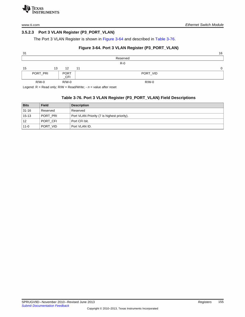
www.ti.com Ethernet Switch Module
155SPRUGV9D–November 2010–Revised June 2013Submit Documentation Feedback
Copyright © 2010–2013, Texas Instruments Incorporated
Registers
3.5.2.3 Port 3 VLAN Register (P3_PORT_VLAN)The Port 3 VLAN Register is shown in Figure 3-64 and described in Table 3-76.
Figure 3-64. Port 3 VLAN Register (P3_PORT_VLAN)31 16
ReservedR-0
15 13 12 11 0PORT_PRI PORT
_CFIPORT_VID
R/W-0 R/W-0 R/W-0Legend: R = Read only; R/W = Read/Write; - n = value after reset
Table 3-76. Port 3 VLAN Register (P3_PORT_VLAN) Field Descriptions
Bits Field Description31-16 Reserved Reserved15-13 PORT_PRI Port VLAN Priority (7 is highest priority).12 PORT_CFI Port CFI bit.11-0 PORT_VID Port VLAN ID.
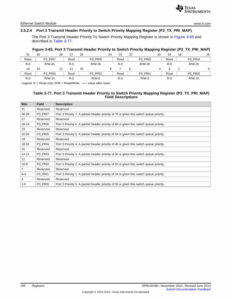
Ethernet Switch Module www.ti.com
156 SPRUGV9D–November 2010–Revised June 2013Submit Documentation Feedback
Copyright © 2010–2013, Texas Instruments Incorporated
Registers
3.5.2.4 Port 3 Transmit Header Priority to Switch Priority Mapping Register (P3_TX_PRI_MAP)The Port 3 Transmit Header Priority To Switch Priority Mapping Register is shown in Figure 3-65 anddescribed in Table 3-77.
Figure 3-65. Port 3 Transmit Header Priority to Switch Priority Mapping Register (P3_TX_PRI_MAP)31 30 28 27 26 24 23 22 20 19 18 16
Reee P3_PRI7 Rsvd P3_PRI6 Rsvd P3_PRI5 Rsvd P3_PRI4R-0 R/W-3h R-0 R/W-3h R-0 R/W-2h R-0 R/W-2h15 14 12 11 10 8 7 6 4 3 2 0
Rsvd P3_PRI3 Rsvd P3_PRI2 Rsvd P3_PRI1 Rsvd P3_PRI0R-0 R/W-1h R-0 R/W-0 R-0 R/W-0 R-0 R/W-1h
Legend: R = Read only; R/W = Read/Write; - n = value after reset
Table 3-77. Port 3 Transmit Header Priority to Switch Priority Mapping Register (P3_TX_PRI_MAP)Field Descriptions
Bits Field Description31 Reserved Reserved30-28 P3_PRI7 Port 3 Priority 7. A packet header priority of 7h is given this switch queue priority.27 Reserved Reserved26-24 P3_PRI6 Port 3 Priority 6. A packet header priority of 6h is given this switch queue priority.23 Reserved Reserved22-20 P3_PRI5 Port 3 Priority 5. A packet header priority of 5h is given this switch queue priority.19 Reserved Reserved18-16 P3_PRI4 Port 3 Priority 4. A packet header priority of 4h is given this switch queue priority.15 Reserved Reserved14-12 P3_PRI3 Port 3 Priority 3. A packet header priority of 3h is given this switch queue priority.11 Reserved Reserved10-8 P3_PRI2 Port 3 Priority 2. A packet header priority of 2h is given this switch queue priority.7 Reserved Reserved6-4 P3_PRI1 Port 3 Priority 1. A packet header priority of 1h is given this switch queue priority.3 Reserved Reserved2-0 P3_PRI0 Port 3 Priority 0. A packet header priority of 0h is given this switch queue priority.

www.ti.com Ethernet Switch Module
157SPRUGV9D–November 2010–Revised June 2013Submit Documentation Feedback
Copyright © 2010–2013, Texas Instruments Incorporated
Registers
3.5.2.5 MAC3 Source Address Low Register (MAC3_SA_LO)The MAC3 Source Address Low Register is shown in Figure 3-66 and described in Table 3-78.
Figure 3-66. MAC3 Source Address Low Register (MAC3_SA_LO)31 16
ReservedR-0
15 8 7 0MACSRCADDR0 MACSRCADDR1
R/W-0 R/W-0Legend: R = Read only; R/W = Read/Write; - n = value after reset
Table 3-78. MAC3 Source Address Low Register (MAC3_SA_LO) Field Descriptions
Bits Field Description31-16 Reserved Reserved15-8 MACSRCADDR0 Source address bits 7-0 (byte 0).7-0 MACSRCADDR1 Source address bits 15-8 (byte 1).
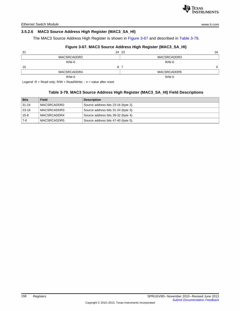
Ethernet Switch Module www.ti.com
158 SPRUGV9D–November 2010–Revised June 2013Submit Documentation Feedback
Copyright © 2010–2013, Texas Instruments Incorporated
Registers
3.5.2.6 MAC3 Source Address High Register (MAC3_SA_HI)The MAC3 Source Address High Register is shown in Figure 3-67 and described in Table 3-79.
Figure 3-67. MAC3 Source Address High Register (MAC3_SA_HI)31 24 23 16
MACSRCADDR2 MACSRCADDR3R/W-0 R/W-0
15 8 7 0MACSRCADDR4 MACSRCADDR5
R/W-0 R/W-0Legend: R = Read only; R/W = Read/Write; - n = value after reset
Table 3-79. MAC3 Source Address High Register (MAC3_SA_HI) Field Descriptions
Bits Field Description31-24 MACSRCADDR2 Source address bits 23-16 (byte 2).23-16 MACSRCADDR3 Source address bits 31-24 (byte 3).15-8 MACSRCADDR4 Source address bits 39-32 (byte 4).7-0 MACSRCADDR5 Source address bits 47-40 (byte 5).
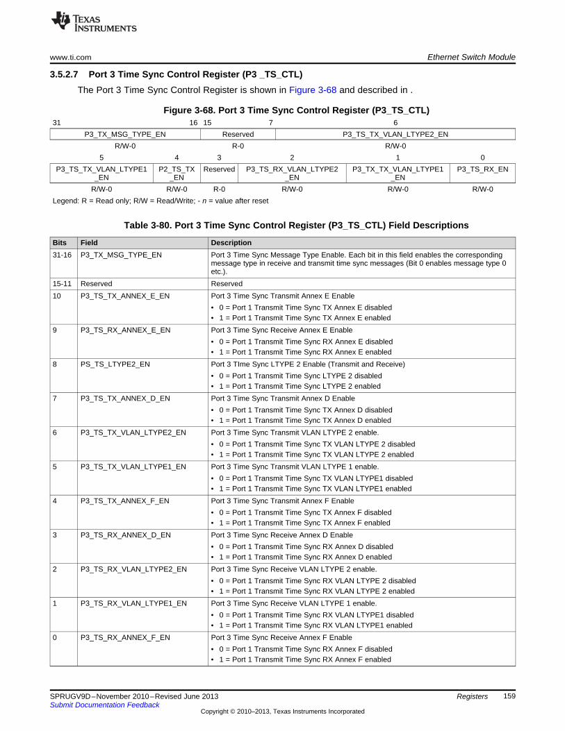
www.ti.com Ethernet Switch Module
159SPRUGV9D–November 2010–Revised June 2013Submit Documentation Feedback
Copyright © 2010–2013, Texas Instruments Incorporated
Registers
3.5.2.7 Port 3 Time Sync Control Register (P3 _TS_CTL)The Port 3 Time Sync Control Register is shown in Figure 3-68 and described in .
Figure 3-68. Port 3 Time Sync Control Register (P3_TS_CTL)31 16 15 7 6
P3_TX_MSG_TYPE_EN Reserved P3_TS_TX_VLAN_LTYPE2_ENR/W-0 R-0 R/W-0
5 4 3 2 1 0P3_TS_TX_VLAN_LTYPE1
_ENP2_TS_TX
_ENReserved P3_TS_RX_VLAN_LTYPE2
_ENP3_TX_TX_VLAN_LTYPE1
_ENP3_TS_RX_EN
R/W-0 R/W-0 R-0 R/W-0 R/W-0 R/W-0Legend: R = Read only; R/W = Read/Write; - n = value after reset
Table 3-80. Port 3 Time Sync Control Register (P3_TS_CTL) Field Descriptions
Bits Field Description31-16 P3_TX_MSG_TYPE_EN Port 3 Time Sync Message Type Enable. Each bit in this field enables the corresponding
message type in receive and transmit time sync messages (Bit 0 enables message type 0etc.).
15-11 Reserved Reserved10 P3_TS_TX_ANNEX_E_EN Port 3 Time Sync Transmit Annex E Enable
• 0 = Port 1 Transmit Time Sync TX Annex E disabled• 1 = Port 1 Transmit Time Sync TX Annex E enabled
9 P3_TS_RX_ANNEX_E_EN Port 3 Time Sync Receive Annex E Enable• 0 = Port 1 Transmit Time Sync RX Annex E disabled• 1 = Port 1 Transmit Time Sync RX Annex E enabled
8 PS_TS_LTYPE2_EN Port 3 TIme Sync LTYPE 2 Enable (Transmit and Receive)• 0 = Port 1 Transmit Time Sync LTYPE 2 disabled• 1 = Port 1 Transmit Time Sync LTYPE 2 enabled
7 P3_TS_TX_ANNEX_D_EN Port 3 Time Sync Transmit Annex D Enable• 0 = Port 1 Transmit Time Sync TX Annex D disabled• 1 = Port 1 Transmit Time Sync TX Annex D enabled
6 P3_TS_TX_VLAN_LTYPE2_EN Port 3 Time Sync Transmit VLAN LTYPE 2 enable.• 0 = Port 1 Transmit Time Sync TX VLAN LTYPE 2 disabled• 1 = Port 1 Transmit Time Sync TX VLAN LTYPE 2 enabled
5 P3_TS_TX_VLAN_LTYPE1_EN Port 3 Time Sync Transmit VLAN LTYPE 1 enable.• 0 = Port 1 Transmit Time Sync TX VLAN LTYPE1 disabled• 1 = Port 1 Transmit Time Sync TX VLAN LTYPE1 enabled
4 P3_TS_TX_ANNEX_F_EN Port 3 Time Sync Transmit Annex F Enable• 0 = Port 1 Transmit Time Sync TX Annex F disabled• 1 = Port 1 Transmit Time Sync TX Annex F enabled
3 P3_TS_RX_ANNEX_D_EN Port 3 Time Sync Receive Annex D Enable• 0 = Port 1 Transmit Time Sync RX Annex D disabled• 1 = Port 1 Transmit Time Sync RX Annex D enabled
2 P3_TS_RX_VLAN_LTYPE2_EN Port 3 Time Sync Receive VLAN LTYPE 2 enable.• 0 = Port 1 Transmit Time Sync RX VLAN LTYPE 2 disabled• 1 = Port 1 Transmit Time Sync RX VLAN LTYPE 2 enabled
1 P3_TS_RX_VLAN_LTYPE1_EN Port 3 Time Sync Receive VLAN LTYPE 1 enable.• 0 = Port 1 Transmit Time Sync RX VLAN LTYPE1 disabled• 1 = Port 1 Transmit Time Sync RX VLAN LTYPE1 enabled
0 P3_TS_RX_ANNEX_F_EN Port 3 Time Sync Receive Annex F Enable• 0 = Port 1 Transmit Time Sync RX Annex F disabled• 1 = Port 1 Transmit Time Sync RX Annex F enabled
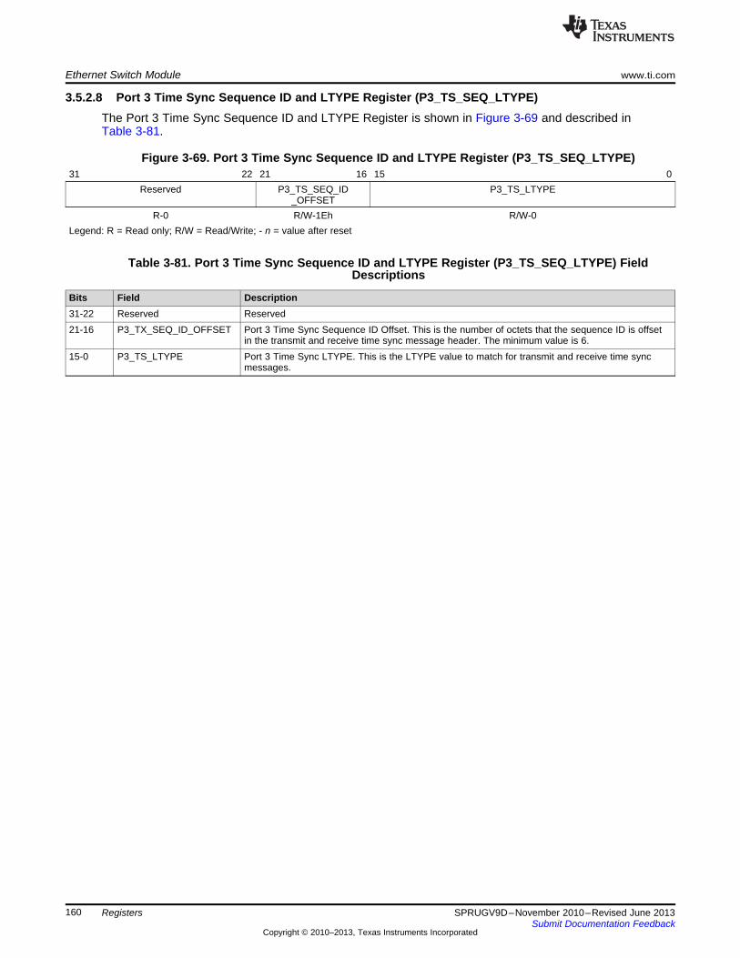
Ethernet Switch Module www.ti.com
160 SPRUGV9D–November 2010–Revised June 2013Submit Documentation Feedback
Copyright © 2010–2013, Texas Instruments Incorporated
Registers
3.5.2.8 Port 3 Time Sync Sequence ID and LTYPE Register (P3_TS_SEQ_LTYPE)The Port 3 Time Sync Sequence ID and LTYPE Register is shown in Figure 3-69 and described inTable 3-81.
Figure 3-69. Port 3 Time Sync Sequence ID and LTYPE Register (P3_TS_SEQ_LTYPE)31 22 21 16 15 0
Reserved P3_TS_SEQ_ID_OFFSET
P3_TS_LTYPE
R-0 R/W-1Eh R/W-0Legend: R = Read only; R/W = Read/Write; - n = value after reset
Table 3-81. Port 3 Time Sync Sequence ID and LTYPE Register (P3_TS_SEQ_LTYPE) FieldDescriptions
Bits Field Description31-22 Reserved Reserved21-16 P3_TX_SEQ_ID_OFFSET Port 3 Time Sync Sequence ID Offset. This is the number of octets that the sequence ID is offset
in the transmit and receive time sync message header. The minimum value is 6.15-0 P3_TS_LTYPE Port 3 Time Sync LTYPE. This is the LTYPE value to match for transmit and receive time sync
messages.
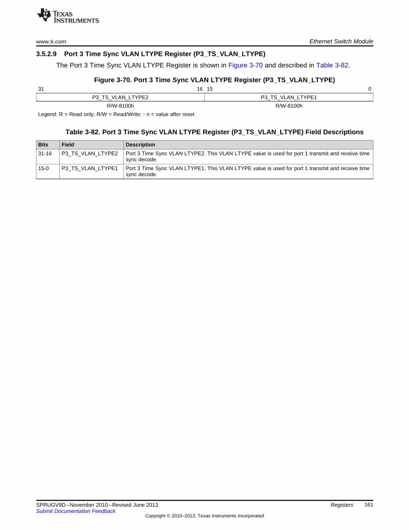
www.ti.com Ethernet Switch Module
161SPRUGV9D–November 2010–Revised June 2013Submit Documentation Feedback
Copyright © 2010–2013, Texas Instruments Incorporated
Registers
3.5.2.9 Port 3 Time Sync VLAN LTYPE Register (P3_TS_VLAN_LTYPE)The Port 3 Time Sync VLAN LTYPE Register is shown in Figure 3-70 and described in Table 3-82.
Figure 3-70. Port 3 Time Sync VLAN LTYPE Register (P3_TS_VLAN_LTYPE)31 16 15 0
P3_TS_VLAN_LTYPE2 P3_TS_VLAN_LTYPE1R/W-8100h R/W-8100h
Legend: R = Read only; R/W = Read/Write; - n = value after reset
Table 3-82. Port 3 Time Sync VLAN LTYPE Register (P3_TS_VLAN_LTYPE) Field Descriptions
Bits Field Description31-16 P3_TS_VLAN_LTYPE2 Port 3 Time Sync VLAN LTYPE2. This VLAN LTYPE value is used for port 1 transmit and receive time
sync decode.15-0 P3_TS_VLAN_LTYPE1 Port 3 Time Sync VLAN LTYPE1. This VLAN LTYPE value is used for port 1 transmit and receive time
sync decode.
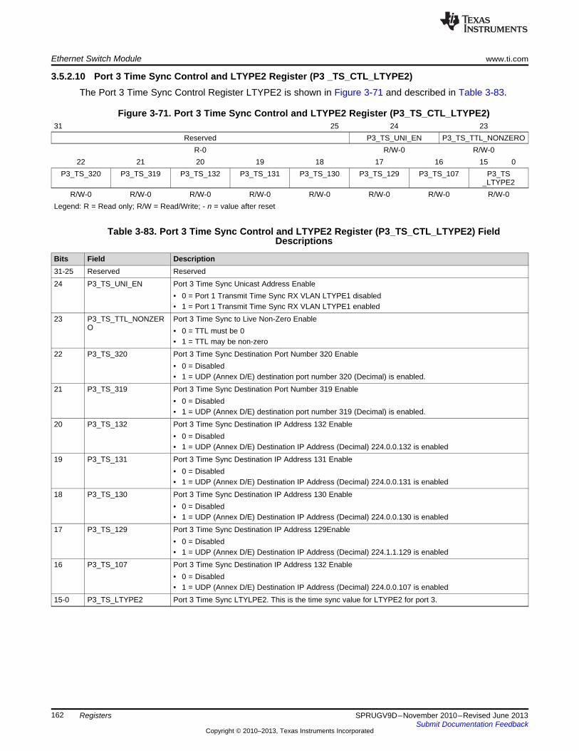
Ethernet Switch Module www.ti.com
162 SPRUGV9D–November 2010–Revised June 2013Submit Documentation Feedback
Copyright © 2010–2013, Texas Instruments Incorporated
Registers
3.5.2.10 Port 3 Time Sync Control and LTYPE2 Register (P3 _TS_CTL_LTYPE2)The Port 3 Time Sync Control Register LTYPE2 is shown in Figure 3-71 and described in Table 3-83.
Figure 3-71. Port 3 Time Sync Control and LTYPE2 Register (P3_TS_CTL_LTYPE2)31 25 24 23
Reserved P3_TS_UNI_EN P3_TS_TTL_NONZEROR-0 R/W-0 R/W-0
22 21 20 19 18 17 16 15 0P3_TS_320 P3_TS_319 P3_TS_132 P3_TS_131 P3_TS_130 P3_TS_129 P3_TS_107 P3_TS
_LTYPE2R/W-0 R/W-0 R/W-0 R/W-0 R/W-0 R/W-0 R/W-0 R/W-0
Legend: R = Read only; R/W = Read/Write; - n = value after reset
Table 3-83. Port 3 Time Sync Control and LTYPE2 Register (P3_TS_CTL_LTYPE2) FieldDescriptions
Bits Field Description31-25 Reserved Reserved24 P3_TS_UNI_EN Port 3 Time Sync Unicast Address Enable
• 0 = Port 1 Transmit Time Sync RX VLAN LTYPE1 disabled• 1 = Port 1 Transmit Time Sync RX VLAN LTYPE1 enabled
23 P3_TS_TTL_NONZERO
Port 3 Time Sync to Live Non-Zero Enable• 0 = TTL must be 0• 1 = TTL may be non-zero
22 P3_TS_320 Port 3 Time Sync Destination Port Number 320 Enable• 0 = Disabled• 1 = UDP (Annex D/E) destination port number 320 (Decimal) is enabled.
21 P3_TS_319 Port 3 Time Sync Destination Port Number 319 Enable• 0 = Disabled• 1 = UDP (Annex D/E) destination port number 319 (Decimal) is enabled.
20 P3_TS_132 Port 3 Time Sync Destination IP Address 132 Enable• 0 = Disabled• 1 = UDP (Annex D/E) Destination IP Address (Decimal) 224.0.0.132 is enabled
19 P3_TS_131 Port 3 Time Sync Destination IP Address 131 Enable• 0 = Disabled• 1 = UDP (Annex D/E) Destination IP Address (Decimal) 224.0.0.131 is enabled
18 P3_TS_130 Port 3 Time Sync Destination IP Address 130 Enable• 0 = Disabled• 1 = UDP (Annex D/E) Destination IP Address (Decimal) 224.0.0.130 is enabled
17 P3_TS_129 Port 3 Time Sync Destination IP Address 129Enable• 0 = Disabled• 1 = UDP (Annex D/E) Destination IP Address (Decimal) 224.1.1.129 is enabled
16 P3_TS_107 Port 3 Time Sync Destination IP Address 132 Enable• 0 = Disabled• 1 = UDP (Annex D/E) Destination IP Address (Decimal) 224.0.0.107 is enabled
15-0 P3_TS_LTYPE2 Port 3 Time Sync LTYLPE2. This is the time sync value for LTYPE2 for port 3.
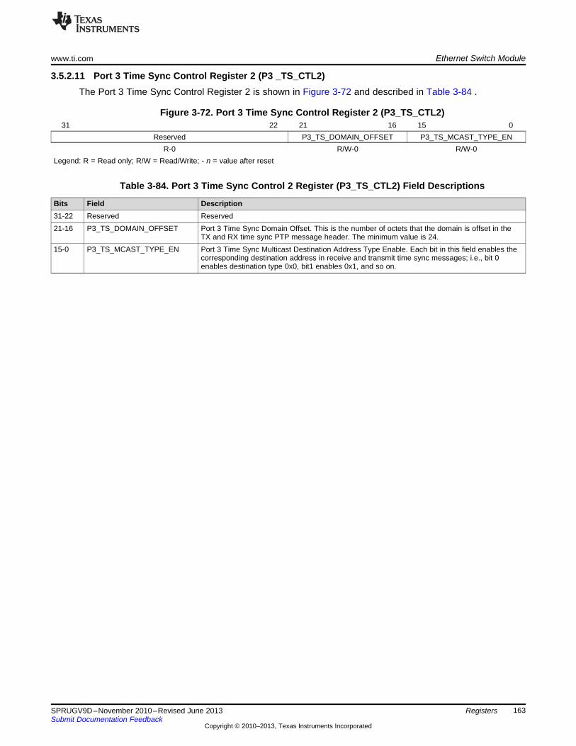
www.ti.com Ethernet Switch Module
163SPRUGV9D–November 2010–Revised June 2013Submit Documentation Feedback
Copyright © 2010–2013, Texas Instruments Incorporated
Registers
3.5.2.11 Port 3 Time Sync Control Register 2 (P3 _TS_CTL2)The Port 3 Time Sync Control Register 2 is shown in Figure 3-72 and described in Table 3-84 .
Figure 3-72. Port 3 Time Sync Control Register 2 (P3_TS_CTL2)31 22 21 16 15 0
Reserved P3_TS_DOMAIN_OFFSET P3_TS_MCAST_TYPE_ENR-0 R/W-0 R/W-0
Legend: R = Read only; R/W = Read/Write; - n = value after reset
Table 3-84. Port 3 Time Sync Control 2 Register (P3_TS_CTL2) Field Descriptions
Bits Field Description31-22 Reserved Reserved21-16 P3_TS_DOMAIN_OFFSET Port 3 Time Sync Domain Offset. This is the number of octets that the domain is offset in the
TX and RX time sync PTP message header. The minimum value is 24.15-0 P3_TS_MCAST_TYPE_EN Port 3 Time Sync Multicast Destination Address Type Enable. Each bit in this field enables the
corresponding destination address in receive and transmit time sync messages; i.e., bit 0enables destination type 0x0, bit1 enables 0x1, and so on.
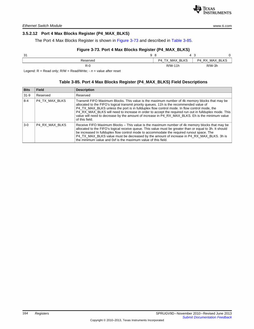
Ethernet Switch Module www.ti.com
164 SPRUGV9D–November 2010–Revised June 2013Submit Documentation Feedback
Copyright © 2010–2013, Texas Instruments Incorporated
Registers
3.5.2.12 Port 4 Max Blocks Register (P4_MAX_BLKS)The Port 4 Max Blocks Register is shown in Figure 3-73 and described in Table 3-85.
Figure 3-73. Port 4 Max Blocks Register (P4_MAX_BLKS)31 9 8 4 3 0
Reserved P4_TX_MAX_BLKS P4_RX_MAX_BLKSR-0 R/W-11h R/W-3h
Legend: R = Read only; R/W = Read/Write; - n = value after reset
Table 3-85. Port 4 Max Blocks Register (P4_MAX_BLKS) Field Descriptions
Bits Field Description31-9 Reserved Reserved8-4 P4_TX_MAX_BLKS Transmit FIFO Maximum Blocks. This value is the maximum number of 4k memory blocks that may be
allocated to the FIFO’s logical transmit priority queues. 11h is the recommended value ofP4_TX_MAX_BLKS unless the port is in fullduplex flow control mode. In flow control mode, theP4_RX_MAX_BLKS will need to increase in order to accept the required run out in fullduplex mode. Thisvalue will need to decrease by the amount of increase in P4_RX_MAX_BLKS. Eh is the minimum valueof this field.
3-0 P4_RX_MAX_BLKS Receive FIFO Maximum Blocks – This value is the maximum number of 4k memory blocks that may beallocated to the FIFO’s logical receive queue. This value must be greater than or equal to 3h. It shouldbe increased In fullduplex flow control mode to accommodate the required runout space. TheP4_TX_MAX_BLKS value must be decreased by the amount of increase in P4_RX_MAX_BLKS. 3h isthe minimum value and 0xf is the maximum value of this field.
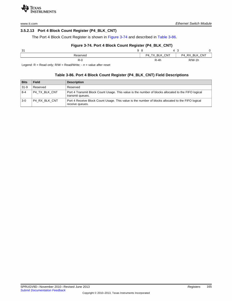
www.ti.com Ethernet Switch Module
165SPRUGV9D–November 2010–Revised June 2013Submit Documentation Feedback
Copyright © 2010–2013, Texas Instruments Incorporated
Registers
3.5.2.13 Port 4 Block Count Register (P4_BLK_CNT)The Port 4 Block Count Register is shown in Figure 3-74 and described in Table 3-86.
Figure 3-74. Port 4 Block Count Register (P4_BLK_CNT)31 9 8 4 3 0
Reserved P4_TX_BLK_CNT P4_RX_BLK_CNTR-0 R-4h R/W-1h
Legend: R = Read only; R/W = Read/Write; - n = value after reset
Table 3-86. Port 4 Block Count Register (P4_BLK_CNT) Field Descriptions
Bits Field Description31-9 Reserved Reserved8-4 P4_TX_BLK_CNT Port 4 Transmit Block Count Usage. This value is the number of blocks allocated to the FIFO logical
transmit queues.3-0 P4_RX_BLK_CNT Port 4 Receive Block Count Usage. This value is the number of blocks allocated to the FIFO logical
receive queues.

Ethernet Switch Module www.ti.com
166 SPRUGV9D–November 2010–Revised June 2013Submit Documentation Feedback
Copyright © 2010–2013, Texas Instruments Incorporated
Registers
3.5.2.14 Port 4 VLAN Register (P4_PORT_VLAN)The Port 4 VLAN Register is shown in Figure 3-75 and described in Table 3-87.
Figure 3-75. Port 4 VLAN Register (P4_PORT_VLAN)31 16
ReservedR-0
15 13 12 11 0PORT_PRI PORT
_CFIPORT_VID
R/W-0 R/W-0 R/W-0Legend: R = Read only; R/W = Read/Write; - n = value after reset
Table 3-87. Port 4 VLAN Register (P4_PORT_VLAN) Field Descriptions
Bits Field Description31-16 Reserved Reserved15-13 PORT_PRI Port VLAN Priority (7 is highest priority).12 PORT_CFI Port CFI bit.11-0 PORT_VID Port VLAN ID.
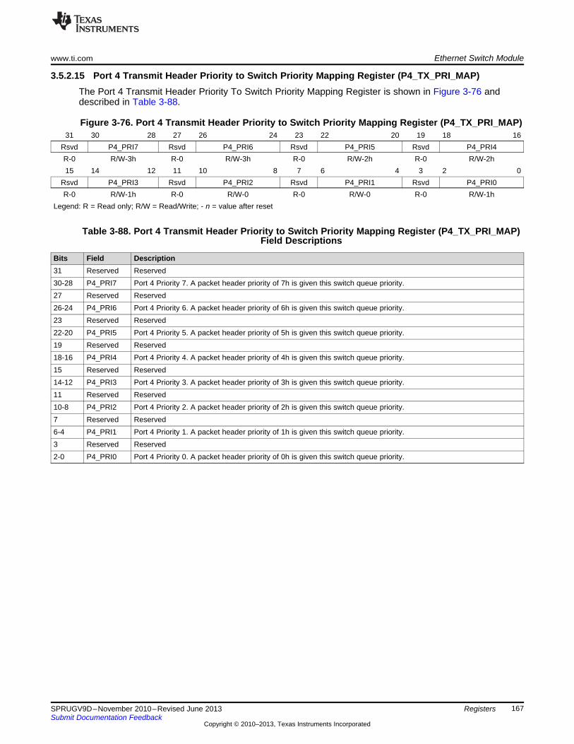
www.ti.com Ethernet Switch Module
167SPRUGV9D–November 2010–Revised June 2013Submit Documentation Feedback
Copyright © 2010–2013, Texas Instruments Incorporated
Registers
3.5.2.15 Port 4 Transmit Header Priority to Switch Priority Mapping Register (P4_TX_PRI_MAP)The Port 4 Transmit Header Priority To Switch Priority Mapping Register is shown in Figure 3-76 anddescribed in Table 3-88.
Figure 3-76. Port 4 Transmit Header Priority to Switch Priority Mapping Register (P4_TX_PRI_MAP)31 30 28 27 26 24 23 22 20 19 18 16
Rsvd P4_PRI7 Rsvd P4_PRI6 Rsvd P4_PRI5 Rsvd P4_PRI4R-0 R/W-3h R-0 R/W-3h R-0 R/W-2h R-0 R/W-2h15 14 12 11 10 8 7 6 4 3 2 0
Rsvd P4_PRI3 Rsvd P4_PRI2 Rsvd P4_PRI1 Rsvd P4_PRI0R-0 R/W-1h R-0 R/W-0 R-0 R/W-0 R-0 R/W-1h
Legend: R = Read only; R/W = Read/Write; - n = value after reset
Table 3-88. Port 4 Transmit Header Priority to Switch Priority Mapping Register (P4_TX_PRI_MAP)Field Descriptions
Bits Field Description31 Reserved Reserved30-28 P4_PRI7 Port 4 Priority 7. A packet header priority of 7h is given this switch queue priority.27 Reserved Reserved26-24 P4_PRI6 Port 4 Priority 6. A packet header priority of 6h is given this switch queue priority.23 Reserved Reserved22-20 P4_PRI5 Port 4 Priority 5. A packet header priority of 5h is given this switch queue priority.19 Reserved Reserved18-16 P4_PRI4 Port 4 Priority 4. A packet header priority of 4h is given this switch queue priority.15 Reserved Reserved14-12 P4_PRI3 Port 4 Priority 3. A packet header priority of 3h is given this switch queue priority.11 Reserved Reserved10-8 P4_PRI2 Port 4 Priority 2. A packet header priority of 2h is given this switch queue priority.7 Reserved Reserved6-4 P4_PRI1 Port 4 Priority 1. A packet header priority of 1h is given this switch queue priority.3 Reserved Reserved2-0 P4_PRI0 Port 4 Priority 0. A packet header priority of 0h is given this switch queue priority.
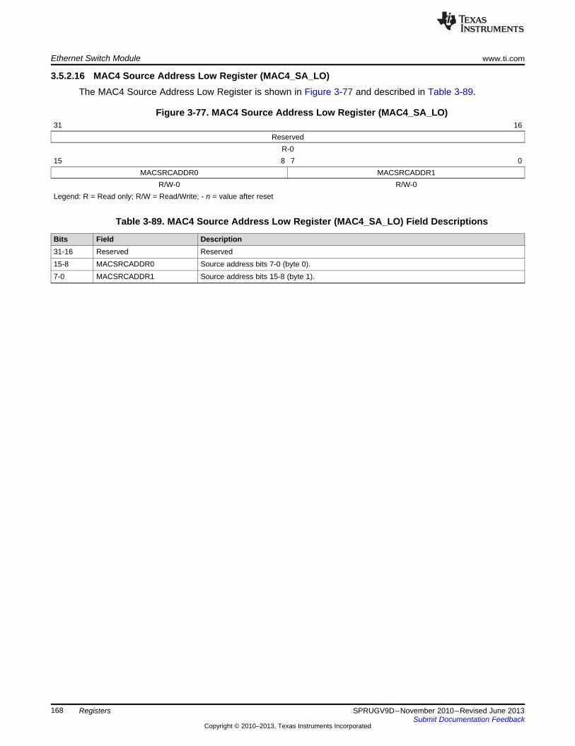
Ethernet Switch Module www.ti.com
168 SPRUGV9D–November 2010–Revised June 2013Submit Documentation Feedback
Copyright © 2010–2013, Texas Instruments Incorporated
Registers
3.5.2.16 MAC4 Source Address Low Register (MAC4_SA_LO)The MAC4 Source Address Low Register is shown in Figure 3-77 and described in Table 3-89.
Figure 3-77. MAC4 Source Address Low Register (MAC4_SA_LO)31 16
ReservedR-0
15 8 7 0MACSRCADDR0 MACSRCADDR1
R/W-0 R/W-0Legend: R = Read only; R/W = Read/Write; - n = value after reset
Table 3-89. MAC4 Source Address Low Register (MAC4_SA_LO) Field Descriptions
Bits Field Description31-16 Reserved Reserved15-8 MACSRCADDR0 Source address bits 7-0 (byte 0).7-0 MACSRCADDR1 Source address bits 15-8 (byte 1).
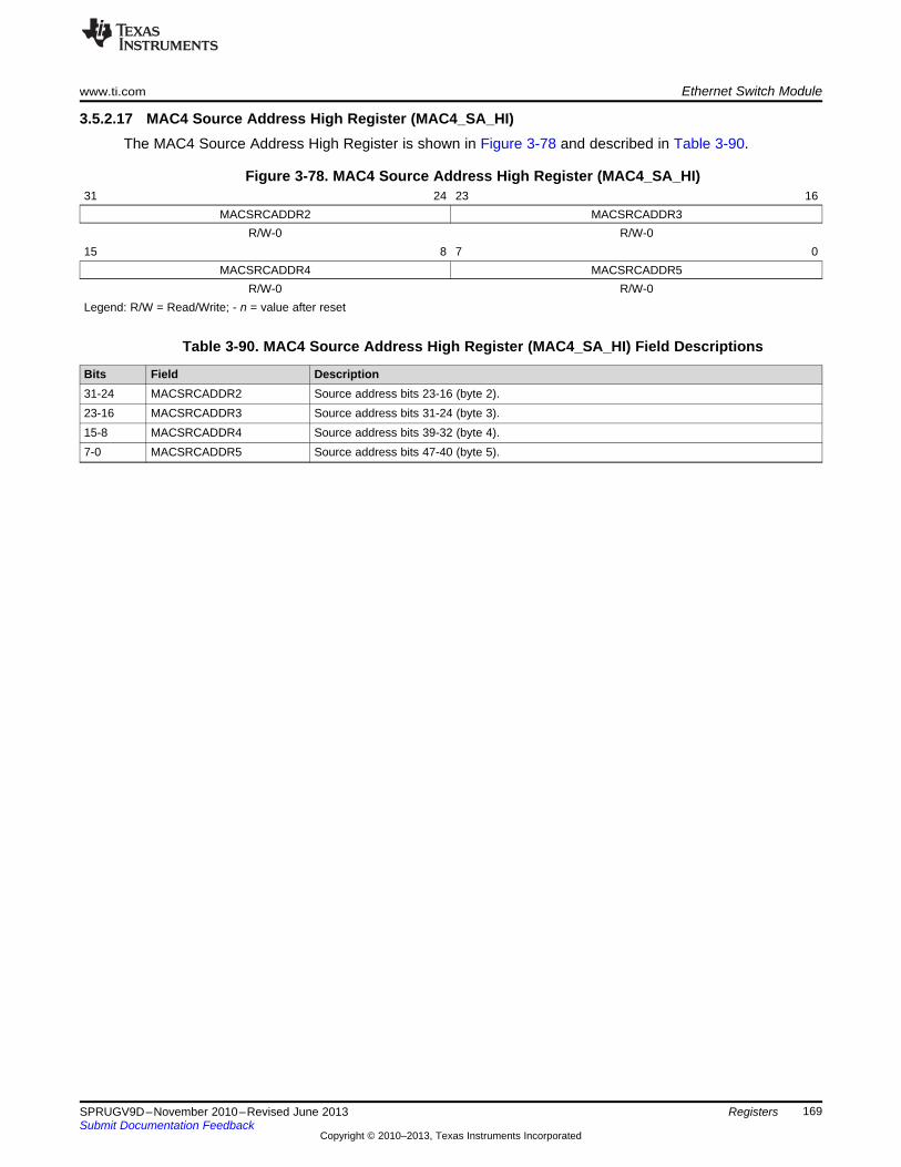
www.ti.com Ethernet Switch Module
169SPRUGV9D–November 2010–Revised June 2013Submit Documentation Feedback
Copyright © 2010–2013, Texas Instruments Incorporated
Registers
3.5.2.17 MAC4 Source Address High Register (MAC4_SA_HI)The MAC4 Source Address High Register is shown in Figure 3-78 and described in Table 3-90.
Figure 3-78. MAC4 Source Address High Register (MAC4_SA_HI)31 24 23 16
MACSRCADDR2 MACSRCADDR3R/W-0 R/W-0
15 8 7 0MACSRCADDR4 MACSRCADDR5
R/W-0 R/W-0Legend: R/W = Read/Write; - n = value after reset
Table 3-90. MAC4 Source Address High Register (MAC4_SA_HI) Field Descriptions
Bits Field Description31-24 MACSRCADDR2 Source address bits 23-16 (byte 2).23-16 MACSRCADDR3 Source address bits 31-24 (byte 3).15-8 MACSRCADDR4 Source address bits 39-32 (byte 4).7-0 MACSRCADDR5 Source address bits 47-40 (byte 5).
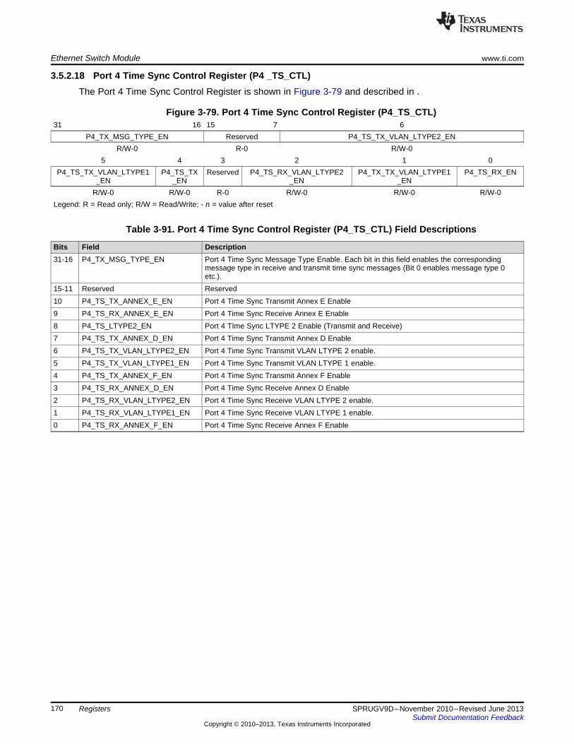
Ethernet Switch Module www.ti.com
170 SPRUGV9D–November 2010–Revised June 2013Submit Documentation Feedback
Copyright © 2010–2013, Texas Instruments Incorporated
Registers
3.5.2.18 Port 4 Time Sync Control Register (P4 _TS_CTL)The Port 4 Time Sync Control Register is shown in Figure 3-79 and described in .
Figure 3-79. Port 4 Time Sync Control Register (P4_TS_CTL)31 16 15 7 6
P4_TX_MSG_TYPE_EN Reserved P4_TS_TX_VLAN_LTYPE2_ENR/W-0 R-0 R/W-0
5 4 3 2 1 0P4_TS_TX_VLAN_LTYPE1
_ENP4_TS_TX
_ENReserved P4_TS_RX_VLAN_LTYPE2
_ENP4_TX_TX_VLAN_LTYPE1
_ENP4_TS_RX_EN
R/W-0 R/W-0 R-0 R/W-0 R/W-0 R/W-0Legend: R = Read only; R/W = Read/Write; - n = value after reset
Table 3-91. Port 4 Time Sync Control Register (P4_TS_CTL) Field Descriptions
Bits Field Description31-16 P4_TX_MSG_TYPE_EN Port 4 Time Sync Message Type Enable. Each bit in this field enables the corresponding
message type in receive and transmit time sync messages (Bit 0 enables message type 0etc.).
15-11 Reserved Reserved10 P4_TS_TX_ANNEX_E_EN Port 4 Time Sync Transmit Annex E Enable9 P4_TS_RX_ANNEX_E_EN Port 4 Time Sync Receive Annex E Enable8 P4_TS_LTYPE2_EN Port 4 TIme Sync LTYPE 2 Enable (Transmit and Receive)7 P4_TS_TX_ANNEX_D_EN Port 4 Time Sync Transmit Annex D Enable6 P4_TS_TX_VLAN_LTYPE2_EN Port 4 Time Sync Transmit VLAN LTYPE 2 enable.5 P4_TS_TX_VLAN_LTYPE1_EN Port 4 Time Sync Transmit VLAN LTYPE 1 enable.4 P4_TS_TX_ANNEX_F_EN Port 4 Time Sync Transmit Annex F Enable3 P4_TS_RX_ANNEX_D_EN Port 4 Time Sync Receive Annex D Enable2 P4_TS_RX_VLAN_LTYPE2_EN Port 4 Time Sync Receive VLAN LTYPE 2 enable.1 P4_TS_RX_VLAN_LTYPE1_EN Port 4 Time Sync Receive VLAN LTYPE 1 enable.0 P4_TS_RX_ANNEX_F_EN Port 4 Time Sync Receive Annex F Enable
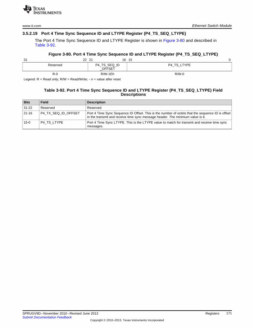
www.ti.com Ethernet Switch Module
171SPRUGV9D–November 2010–Revised June 2013Submit Documentation Feedback
Copyright © 2010–2013, Texas Instruments Incorporated
Registers
3.5.2.19 Port 4 Time Sync Sequence ID and LTYPE Register (P4_TS_SEQ_LTYPE)The Port 4 Time Sync Sequence ID and LTYPE Register is shown in Figure 3-80 and described inTable 3-92.
Figure 3-80. Port 4 Time Sync Sequence ID and LTYPE Register (P4_TS_SEQ_LTYPE)31 22 21 16 15 0
Reserved P4_TS_SEQ_ID_OFFSET
P4_TS_LTYPE
R-0 R/W-1Eh R/W-0Legend: R = Read only; R/W = Read/Write; - n = value after reset
Table 3-92. Port 4 Time Sync Sequence ID and LTYPE Register (P4_TS_SEQ_LTYPE) FieldDescriptions
Bits Field Description31-22 Reserved Reserved21-16 P4_TX_SEQ_ID_OFFSET Port 4 Time Sync Sequence ID Offset. This is the number of octets that the sequence ID is offset
in the transmit and receive time sync message header. The minimum value is 6.15-0 P4_TS_LTYPE Port 4 Time Sync LTYPE. This is the LTYPE value to match for transmit and receive time sync
messages.
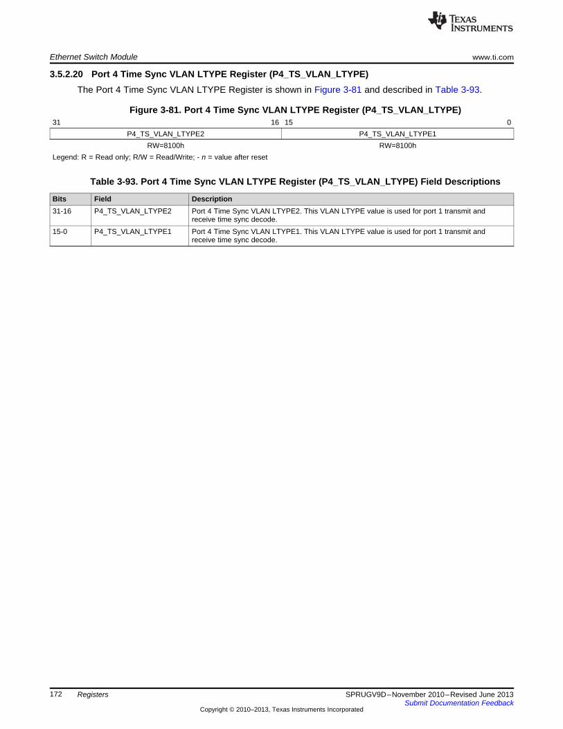
Ethernet Switch Module www.ti.com
172 SPRUGV9D–November 2010–Revised June 2013Submit Documentation Feedback
Copyright © 2010–2013, Texas Instruments Incorporated
Registers
3.5.2.20 Port 4 Time Sync VLAN LTYPE Register (P4_TS_VLAN_LTYPE)The Port 4 Time Sync VLAN LTYPE Register is shown in Figure 3-81 and described in Table 3-93.
Figure 3-81. Port 4 Time Sync VLAN LTYPE Register (P4_TS_VLAN_LTYPE)31 16 15 0
P4_TS_VLAN_LTYPE2 P4_TS_VLAN_LTYPE1RW=8100h RW=8100h
Legend: R = Read only; R/W = Read/Write; - n = value after reset
Table 3-93. Port 4 Time Sync VLAN LTYPE Register (P4_TS_VLAN_LTYPE) Field Descriptions
Bits Field Description31-16 P4_TS_VLAN_LTYPE2 Port 4 Time Sync VLAN LTYPE2. This VLAN LTYPE value is used for port 1 transmit and
receive time sync decode.15-0 P4_TS_VLAN_LTYPE1 Port 4 Time Sync VLAN LTYPE1. This VLAN LTYPE value is used for port 1 transmit and
receive time sync decode.
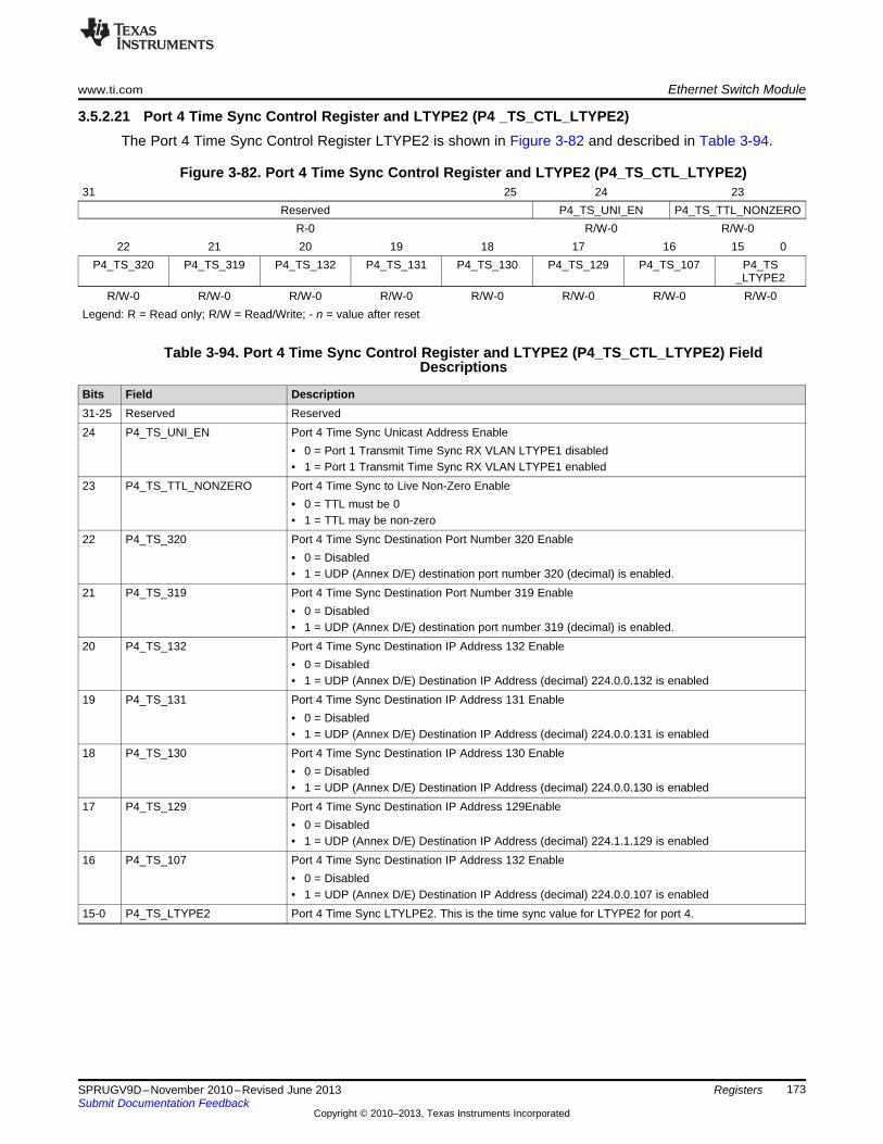
www.ti.com Ethernet Switch Module
173SPRUGV9D–November 2010–Revised June 2013Submit Documentation Feedback
Copyright © 2010–2013, Texas Instruments Incorporated
Registers
3.5.2.21 Port 4 Time Sync Control Register and LTYPE2 (P4 _TS_CTL_LTYPE2)The Port 4 Time Sync Control Register LTYPE2 is shown in Figure 3-82 and described in Table 3-94.
Figure 3-82. Port 4 Time Sync Control Register and LTYPE2 (P4_TS_CTL_LTYPE2)31 25 24 23
Reserved P4_TS_UNI_EN P4_TS_TTL_NONZEROR-0 R/W-0 R/W-0
22 21 20 19 18 17 16 15 0P4_TS_320 P4_TS_319 P4_TS_132 P4_TS_131 P4_TS_130 P4_TS_129 P4_TS_107 P4_TS
_LTYPE2R/W-0 R/W-0 R/W-0 R/W-0 R/W-0 R/W-0 R/W-0 R/W-0
Legend: R = Read only; R/W = Read/Write; - n = value after reset
Table 3-94. Port 4 Time Sync Control Register and LTYPE2 (P4_TS_CTL_LTYPE2) FieldDescriptions
Bits Field Description31-25 Reserved Reserved24 P4_TS_UNI_EN Port 4 Time Sync Unicast Address Enable
• 0 = Port 1 Transmit Time Sync RX VLAN LTYPE1 disabled• 1 = Port 1 Transmit Time Sync RX VLAN LTYPE1 enabled
23 P4_TS_TTL_NONZERO Port 4 Time Sync to Live Non-Zero Enable• 0 = TTL must be 0• 1 = TTL may be non-zero
22 P4_TS_320 Port 4 Time Sync Destination Port Number 320 Enable• 0 = Disabled• 1 = UDP (Annex D/E) destination port number 320 (decimal) is enabled.
21 P4_TS_319 Port 4 Time Sync Destination Port Number 319 Enable• 0 = Disabled• 1 = UDP (Annex D/E) destination port number 319 (decimal) is enabled.
20 P4_TS_132 Port 4 Time Sync Destination IP Address 132 Enable• 0 = Disabled• 1 = UDP (Annex D/E) Destination IP Address (decimal) 224.0.0.132 is enabled
19 P4_TS_131 Port 4 Time Sync Destination IP Address 131 Enable• 0 = Disabled• 1 = UDP (Annex D/E) Destination IP Address (decimal) 224.0.0.131 is enabled
18 P4_TS_130 Port 4 Time Sync Destination IP Address 130 Enable• 0 = Disabled• 1 = UDP (Annex D/E) Destination IP Address (decimal) 224.0.0.130 is enabled
17 P4_TS_129 Port 4 Time Sync Destination IP Address 129Enable• 0 = Disabled• 1 = UDP (Annex D/E) Destination IP Address (decimal) 224.1.1.129 is enabled
16 P4_TS_107 Port 4 Time Sync Destination IP Address 132 Enable• 0 = Disabled• 1 = UDP (Annex D/E) Destination IP Address (decimal) 224.0.0.107 is enabled
15-0 P4_TS_LTYPE2 Port 4 Time Sync LTYLPE2. This is the time sync value for LTYPE2 for port 4.
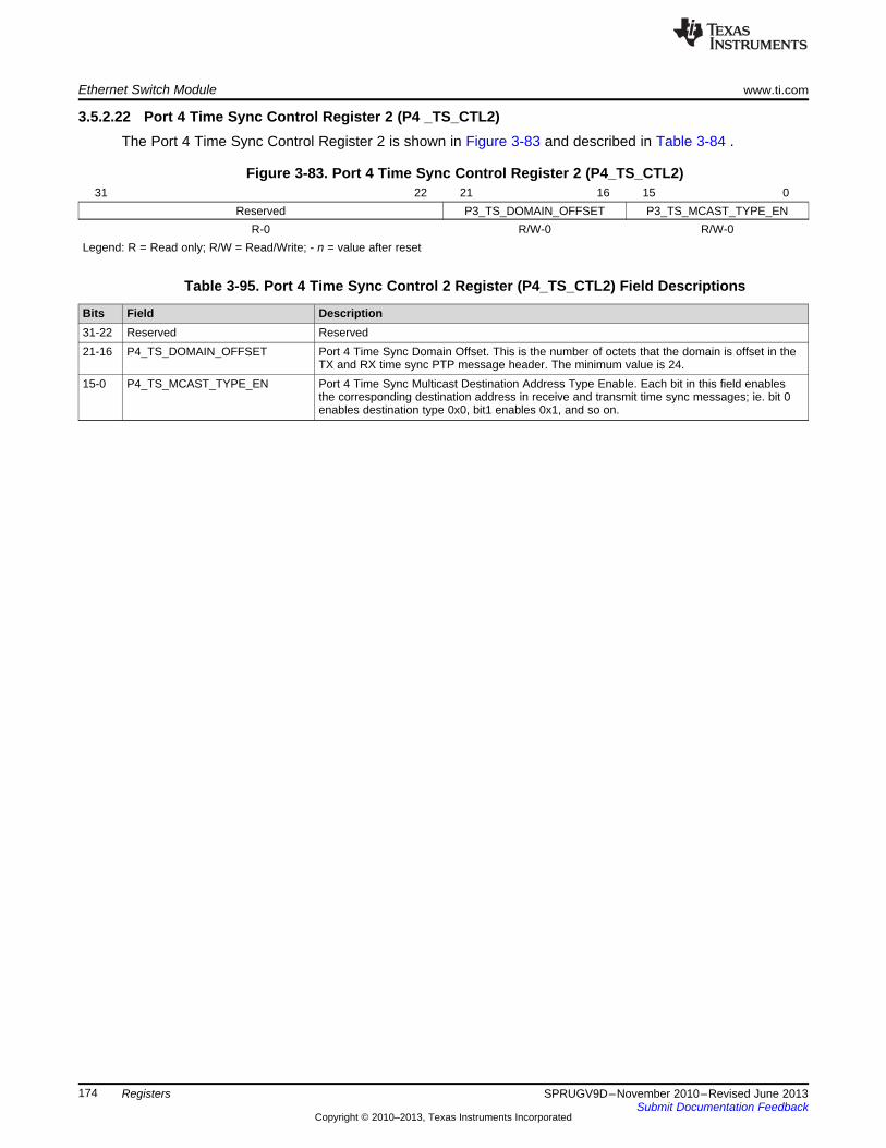
Ethernet Switch Module www.ti.com
174 SPRUGV9D–November 2010–Revised June 2013Submit Documentation Feedback
Copyright © 2010–2013, Texas Instruments Incorporated
Registers
3.5.2.22 Port 4 Time Sync Control Register 2 (P4 _TS_CTL2)The Port 4 Time Sync Control Register 2 is shown in Figure 3-83 and described in Table 3-84 .
Figure 3-83. Port 4 Time Sync Control Register 2 (P4_TS_CTL2)31 22 21 16 15 0
Reserved P3_TS_DOMAIN_OFFSET P3_TS_MCAST_TYPE_ENR-0 R/W-0 R/W-0
Legend: R = Read only; R/W = Read/Write; - n = value after reset
Table 3-95. Port 4 Time Sync Control 2 Register (P4_TS_CTL2) Field Descriptions
Bits Field Description31-22 Reserved Reserved21-16 P4_TS_DOMAIN_OFFSET Port 4 Time Sync Domain Offset. This is the number of octets that the domain is offset in the
TX and RX time sync PTP message header. The minimum value is 24.15-0 P4_TS_MCAST_TYPE_EN Port 4 Time Sync Multicast Destination Address Type Enable. Each bit in this field enables
the corresponding destination address in receive and transmit time sync messages; ie. bit 0enables destination type 0x0, bit1 enables 0x1, and so on.
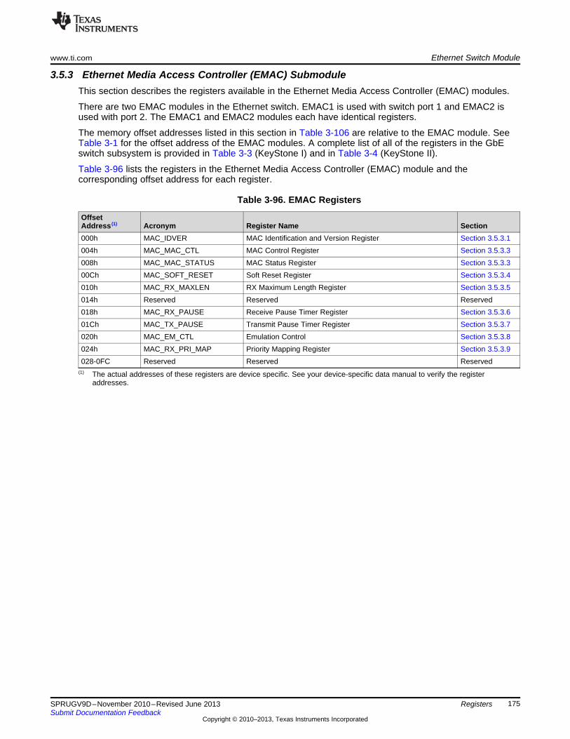
www.ti.com Ethernet Switch Module
175SPRUGV9D–November 2010–Revised June 2013Submit Documentation Feedback
Copyright © 2010–2013, Texas Instruments Incorporated
Registers
3.5.3 Ethernet Media Access Controller (EMAC) SubmoduleThis section describes the registers available in the Ethernet Media Access Controller (EMAC) modules.
There are two EMAC modules in the Ethernet switch. EMAC1 is used with switch port 1 and EMAC2 isused with port 2. The EMAC1 and EMAC2 modules each have identical registers.
The memory offset addresses listed in this section in Table 3-106 are relative to the EMAC module. SeeTable 3-1 for the offset address of the EMAC modules. A complete list of all of the registers in the GbEswitch subsystem is provided in Table 3-3 (KeyStone I) and in Table 3-4 (KeyStone II).
Table 3-96 lists the registers in the Ethernet Media Access Controller (EMAC) module and thecorresponding offset address for each register.
(1) The actual addresses of these registers are device specific. See your device-specific data manual to verify the registeraddresses.
Table 3-96. EMAC Registers
OffsetAddress (1) Acronym Register Name Section000h MAC_IDVER MAC Identification and Version Register Section 3.5.3.1004h MAC_MAC_CTL MAC Control Register Section 3.5.3.3008h MAC_MAC_STATUS MAC Status Register Section 3.5.3.300Ch MAC_SOFT_RESET Soft Reset Register Section 3.5.3.4010h MAC_RX_MAXLEN RX Maximum Length Register Section 3.5.3.5014h Reserved Reserved Reserved018h MAC_RX_PAUSE Receive Pause Timer Register Section 3.5.3.601Ch MAC_TX_PAUSE Transmit Pause Timer Register Section 3.5.3.7020h MAC_EM_CTL Emulation Control Section 3.5.3.8024h MAC_RX_PRI_MAP Priority Mapping Register Section 3.5.3.9028-0FC Reserved Reserved Reserved
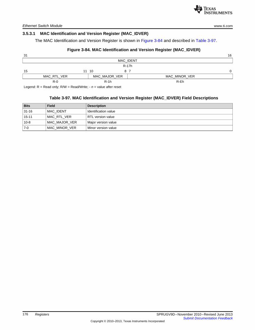
Ethernet Switch Module www.ti.com
176 SPRUGV9D–November 2010–Revised June 2013Submit Documentation Feedback
Copyright © 2010–2013, Texas Instruments Incorporated
Registers
3.5.3.1 MAC Identification and Version Register (MAC_IDVER)The MAC Identification and Version Register is shown in Figure 3-84 and described in Table 3-97.
Figure 3-84. MAC Identification and Version Register (MAC_IDVER)31 16
MAC_IDENTR-17h
15 11 10 8 7 0MAC_RTL_VER MAC_MAJOR_VER MAC_MINOR_VER
R-0 R-1h R-EhLegend: R = Read only; R/W = Read/Write; - n = value after reset
Table 3-97. MAC Identification and Version Register (MAC_IDVER) Field Descriptions
Bits Field Description31-16 MAC_IDENT Identification value15-11 MAC_RTL_VER RTL version value10-8 MAC_MAJOR_VER Major version value7-0 MAC_MINOR_VER Minor version value
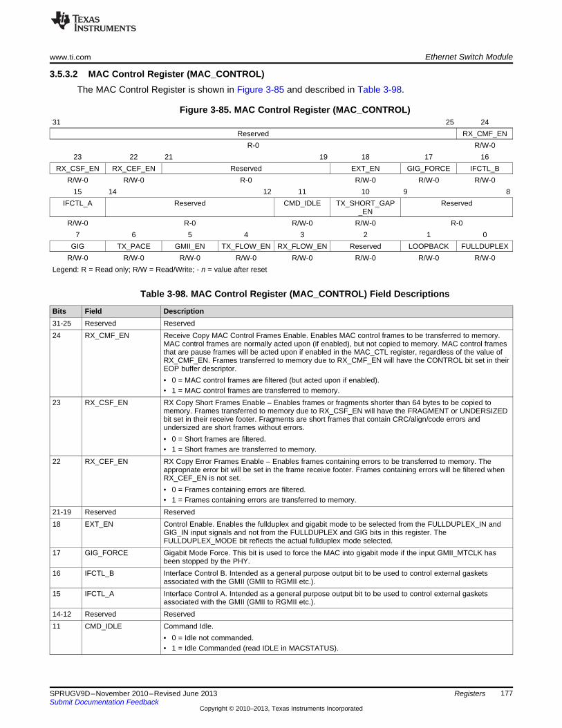
www.ti.com Ethernet Switch Module
177SPRUGV9D–November 2010–Revised June 2013Submit Documentation Feedback
Copyright © 2010–2013, Texas Instruments Incorporated
Registers
3.5.3.2 MAC Control Register (MAC_CONTROL)The MAC Control Register is shown in Figure 3-85 and described in Table 3-98.
Figure 3-85. MAC Control Register (MAC_CONTROL)31 25 24
Reserved RX_CMF_ENR-0 R/W-0
23 22 21 19 18 17 16RX_CSF_EN RX_CEF_EN Reserved EXT_EN GIG_FORCE IFCTL_B
R/W-0 R/W-0 R-0 R/W-0 R/W-0 R/W-015 14 12 11 10 9 8
IFCTL_A Reserved CMD_IDLE TX_SHORT_GAP_EN
Reserved
R/W-0 R-0 R/W-0 R/W-0 R-07 6 5 4 3 2 1 0
GIG TX_PACE GMII_EN TX_FLOW_EN RX_FLOW_EN Reserved LOOPBACK FULLDUPLEXR/W-0 R/W-0 R/W-0 R/W-0 R/W-0 R/W-0 R/W-0 R/W-0
Legend: R = Read only; R/W = Read/Write; - n = value after reset
Table 3-98. MAC Control Register (MAC_CONTROL) Field Descriptions
Bits Field Description31-25 Reserved Reserved24 RX_CMF_EN Receive Copy MAC Control Frames Enable. Enables MAC control frames to be transferred to memory.
MAC control frames are normally acted upon (if enabled), but not copied to memory. MAC control framesthat are pause frames will be acted upon if enabled in the MAC_CTL register, regardless of the value ofRX_CMF_EN. Frames transferred to memory due to RX_CMF_EN will have the CONTROL bit set in theirEOP buffer descriptor.• 0 = MAC control frames are filtered (but acted upon if enabled).• 1 = MAC control frames are transferred to memory.
23 RX_CSF_EN RX Copy Short Frames Enable – Enables frames or fragments shorter than 64 bytes to be copied tomemory. Frames transferred to memory due to RX_CSF_EN will have the FRAGMENT or UNDERSIZEDbit set in their receive footer. Fragments are short frames that contain CRC/align/code errors andundersized are short frames without errors.• 0 = Short frames are filtered.• 1 = Short frames are transferred to memory.
22 RX_CEF_EN RX Copy Error Frames Enable – Enables frames containing errors to be transferred to memory. Theappropriate error bit will be set in the frame receive footer. Frames containing errors will be filtered whenRX_CEF_EN is not set.• 0 = Frames containing errors are filtered.• 1 = Frames containing errors are transferred to memory.
21-19 Reserved Reserved18 EXT_EN Control Enable. Enables the fullduplex and gigabit mode to be selected from the FULLDUPLEX_IN and
GIG_IN input signals and not from the FULLDUPLEX and GIG bits in this register. TheFULLDUPLEX_MODE bit reflects the actual fullduplex mode selected.
17 GIG_FORCE Gigabit Mode Force. This bit is used to force the MAC into gigabit mode if the input GMII_MTCLK hasbeen stopped by the PHY.
16 IFCTL_B Interface Control B. Intended as a general purpose output bit to be used to control external gasketsassociated with the GMII (GMII to RGMII etc.).
15 IFCTL_A Interface Control A. Intended as a general purpose output bit to be used to control external gasketsassociated with the GMII (GMII to RGMII etc.).
14-12 Reserved Reserved11 CMD_IDLE Command Idle.
• 0 = Idle not commanded.• 1 = Idle Commanded (read IDLE in MACSTATUS).
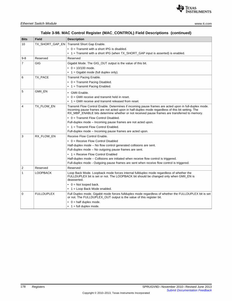
Ethernet Switch Module www.ti.com
178 SPRUGV9D–November 2010–Revised June 2013Submit Documentation Feedback
Copyright © 2010–2013, Texas Instruments Incorporated
Registers
Table 3-98. MAC Control Register (MAC_CONTROL) Field Descriptions (continued)Bits Field Description10 TX_SHORT_GAP_EN Transmit Short Gap Enable.
• 0 = Transmit with a short IPG is disabled.• 1 = Transmit with a short IPG (when TX_SHORT_GAP input is asserted) is enabled.
9-8 Reserved Reserved7 GIG Gigabit Mode. The GIG_OUT output is the value of this bit.
• 0 = 10/100 mode.• 1 = Gigabit mode (full duplex only).
6 TX_PACE Transmit Pacing Enable.• 0 = Transmit Pacing Disabled.• 1 = Transmit Pacing Enabled.
5 GMII_EN • GMII Enable.• 0 = GMII receive and transmit held in reset.• 1 = GMII receive and transmit released from reset.
4 TX_FLOW_EN Transmit Flow Control Enable. Determines if incoming pause frames are acted upon in full-duplex mode.Incoming pause frames are not acted upon in half-duplex mode regardless of this bit setting. TheRX_MBP_ENABLE bits determine whether or not received pause frames are transferred to memory.• 0 = Transmit Flow Control Disabled.Full-duplex mode – Incoming pause frames are not acted upon.• 1 = Transmit Flow Control Enabled.Full-duplex mode – Incoming pause frames are acted upon.
3 RX_FLOW_EN Receive Flow Control Enable.• 0 = Receive Flow Control DisabledHalf-duplex mode – No flow control generated collisions are sent.Full-duplex mode – No outgoing pause frames are sent.• 1 = Receive Flow Control EnabledHalf-duplex mode – Collisions are initiated when receive flow control is triggered.Full-duplex mode - Outgoing pause frames are sent when receive flow control is triggered.
2 Reserved Reserved1 LOOPBACK Loop Back Mode. Loopback mode forces internal fullduplex mode regardless of whether the
FULLDUPLEX bit is set or not. The LOOPBACK bit should be changed only when GMII_EN isdeasserted.• 0 = Not looped back.• 1 = Loop Back Mode enabled.
0 FULLDUPLEX Full Duplex mode. Gigabit mode forces fullduplex mode regardless of whether the FULLDUPLEX bit is setor not. The FULLDUPLEX_OUT output is the value of this register bit.• 0 = half duplex mode.• 1 = full duplex mode.
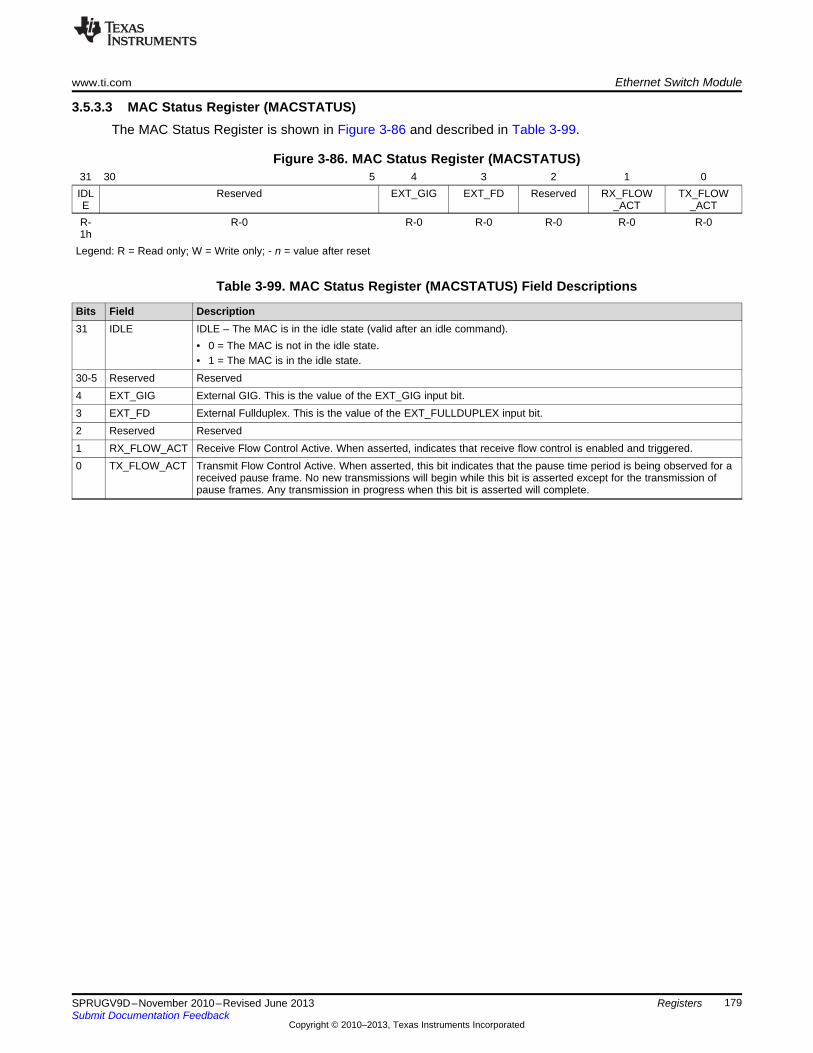
www.ti.com Ethernet Switch Module
179SPRUGV9D–November 2010–Revised June 2013Submit Documentation Feedback
Copyright © 2010–2013, Texas Instruments Incorporated
Registers
3.5.3.3 MAC Status Register (MACSTATUS)The MAC Status Register is shown in Figure 3-86 and described in Table 3-99.
Figure 3-86. MAC Status Register (MACSTATUS)31 30 5 4 3 2 1 0IDLE
Reserved EXT_GIG EXT_FD Reserved RX_FLOW_ACT
TX_FLOW_ACT
R-1h
R-0 R-0 R-0 R-0 R-0 R-0
Legend: R = Read only; W = Write only; - n = value after reset
Table 3-99. MAC Status Register (MACSTATUS) Field Descriptions
Bits Field Description31 IDLE IDLE – The MAC is in the idle state (valid after an idle command).
• 0 = The MAC is not in the idle state.• 1 = The MAC is in the idle state.
30-5 Reserved Reserved4 EXT_GIG External GIG. This is the value of the EXT_GIG input bit.3 EXT_FD External Fullduplex. This is the value of the EXT_FULLDUPLEX input bit.2 Reserved Reserved1 RX_FLOW_ACT Receive Flow Control Active. When asserted, indicates that receive flow control is enabled and triggered.0 TX_FLOW_ACT Transmit Flow Control Active. When asserted, this bit indicates that the pause time period is being observed for a
received pause frame. No new transmissions will begin while this bit is asserted except for the transmission ofpause frames. Any transmission in progress when this bit is asserted will complete.
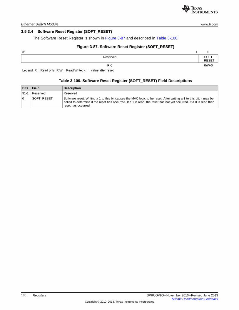
Ethernet Switch Module www.ti.com
180 SPRUGV9D–November 2010–Revised June 2013Submit Documentation Feedback
Copyright © 2010–2013, Texas Instruments Incorporated
Registers
3.5.3.4 Software Reset Register (SOFT_RESET)The Software Reset Register is shown in Figure 3-87 and described in Table 3-100.
Figure 3-87. Software Reset Register (SOFT_RESET)31 1 0
Reserved SOFT_RESET
R-0 R/W-0Legend: R = Read only; R/W = Read/Write; - n = value after reset
Table 3-100. Software Reset Register (SOFT_RESET) Field Descriptions
Bits Field Description31-1 Reserved Reserved0 SOFT_RESET Software reset. Writing a 1 to this bit causes the MAC logic to be reset. After writing a 1 to this bit, it may be
polled to determine if the reset has occurred. If a 1 is read, the reset has not yet occurred. If a 0 is read thenreset has occurred.
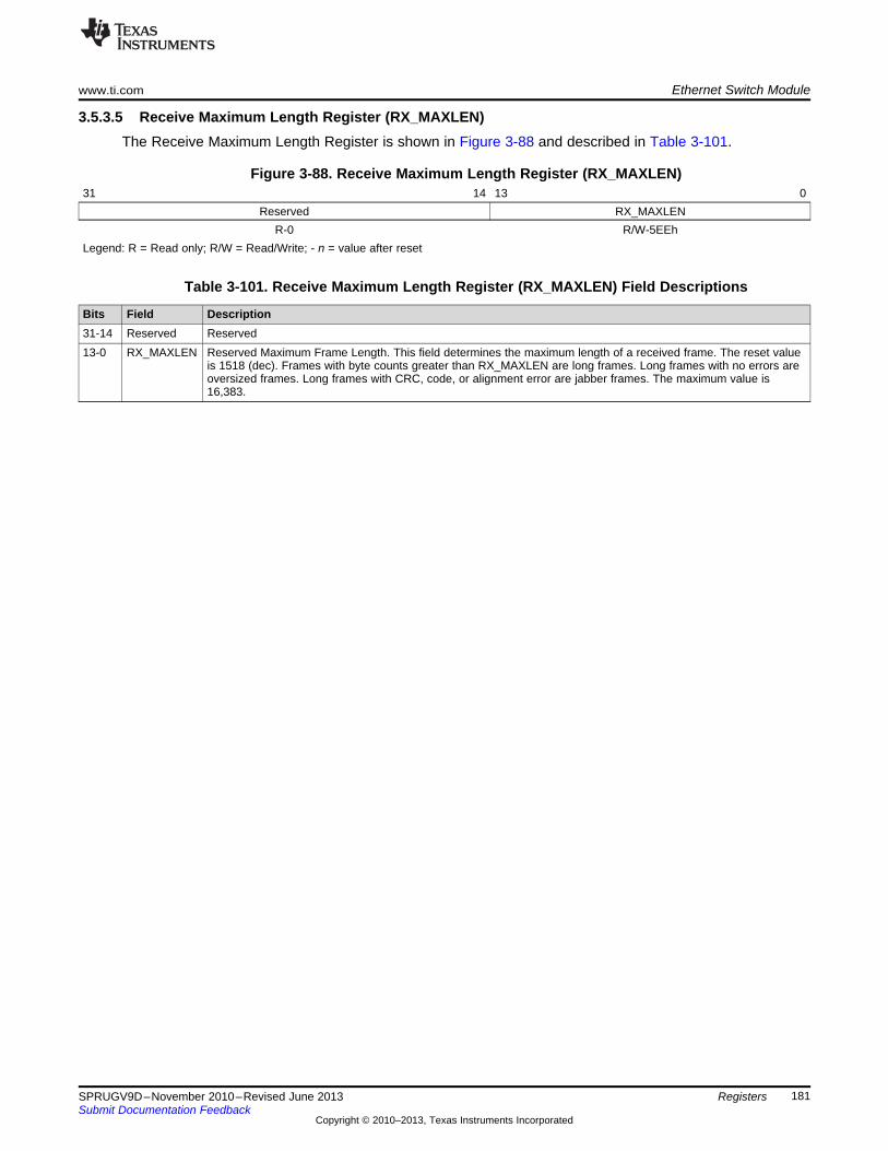
www.ti.com Ethernet Switch Module
181SPRUGV9D–November 2010–Revised June 2013Submit Documentation Feedback
Copyright © 2010–2013, Texas Instruments Incorporated
Registers
3.5.3.5 Receive Maximum Length Register (RX_MAXLEN)The Receive Maximum Length Register is shown in Figure 3-88 and described in Table 3-101.
Figure 3-88. Receive Maximum Length Register (RX_MAXLEN)31 14 13 0
Reserved RX_MAXLENR-0 R/W-5EEh
Legend: R = Read only; R/W = Read/Write; - n = value after reset
Table 3-101. Receive Maximum Length Register (RX_MAXLEN) Field Descriptions
Bits Field Description31-14 Reserved Reserved13-0 RX_MAXLEN Reserved Maximum Frame Length. This field determines the maximum length of a received frame. The reset value
is 1518 (dec). Frames with byte counts greater than RX_MAXLEN are long frames. Long frames with no errors areoversized frames. Long frames with CRC, code, or alignment error are jabber frames. The maximum value is16,383.
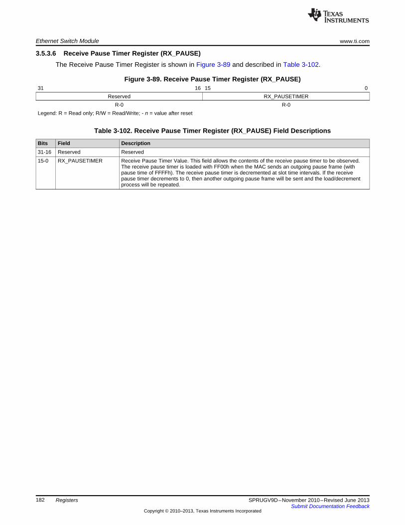
Ethernet Switch Module www.ti.com
182 SPRUGV9D–November 2010–Revised June 2013Submit Documentation Feedback
Copyright © 2010–2013, Texas Instruments Incorporated
Registers
3.5.3.6 Receive Pause Timer Register (RX_PAUSE)The Receive Pause Timer Register is shown in Figure 3-89 and described in Table 3-102.
Figure 3-89. Receive Pause Timer Register (RX_PAUSE)31 16 15 0
Reserved RX_PAUSETIMERR-0 R-0
Legend: R = Read only; R/W = Read/Write; - n = value after reset
Table 3-102. Receive Pause Timer Register (RX_PAUSE) Field Descriptions
Bits Field Description31-16 Reserved Reserved15-0 RX_PAUSETIMER Receive Pause Timer Value. This field allows the contents of the receive pause timer to be observed.
The receive pause timer is loaded with FF00h when the MAC sends an outgoing pause frame (withpause time of FFFFh). The receive pause timer is decremented at slot time intervals. If the receivepause timer decrements to 0, then another outgoing pause frame will be sent and the load/decrementprocess will be repeated.
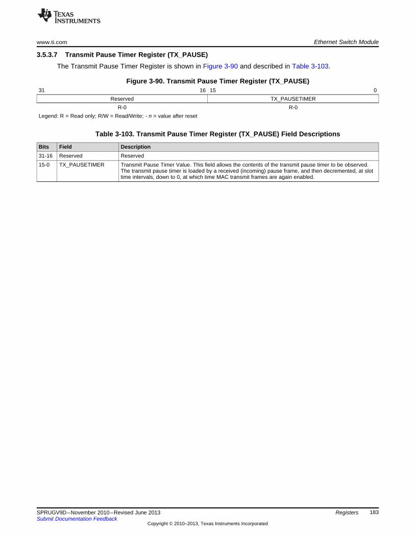
www.ti.com Ethernet Switch Module
183SPRUGV9D–November 2010–Revised June 2013Submit Documentation Feedback
Copyright © 2010–2013, Texas Instruments Incorporated
Registers
3.5.3.7 Transmit Pause Timer Register (TX_PAUSE)The Transmit Pause Timer Register is shown in Figure 3-90 and described in Table 3-103.
Figure 3-90. Transmit Pause Timer Register (TX_PAUSE)31 16 15 0
Reserved TX_PAUSETIMERR-0 R-0
Legend: R = Read only; R/W = Read/Write; - n = value after reset
Table 3-103. Transmit Pause Timer Register (TX_PAUSE) Field Descriptions
Bits Field Description31-16 Reserved Reserved15-0 TX_PAUSETIMER Transmit Pause Timer Value. This field allows the contents of the transmit pause timer to be observed.
The transmit pause timer is loaded by a received (incoming) pause frame, and then decremented, at slottime intervals, down to 0, at which time MAC transmit frames are again enabled.
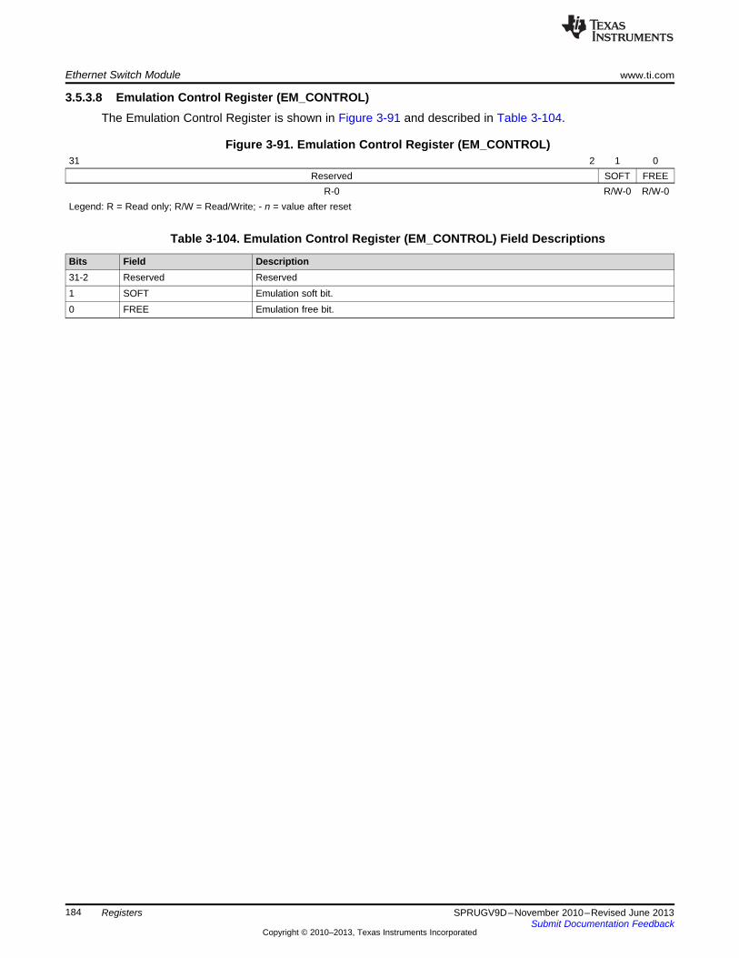
Ethernet Switch Module www.ti.com
184 SPRUGV9D–November 2010–Revised June 2013Submit Documentation Feedback
Copyright © 2010–2013, Texas Instruments Incorporated
Registers
3.5.3.8 Emulation Control Register (EM_CONTROL)The Emulation Control Register is shown in Figure 3-91 and described in Table 3-104.
Figure 3-91. Emulation Control Register (EM_CONTROL)31 2 1 0
Reserved SOFT FREER-0 R/W-0 R/W-0
Legend: R = Read only; R/W = Read/Write; - n = value after reset
Table 3-104. Emulation Control Register (EM_CONTROL) Field Descriptions
Bits Field Description31-2 Reserved Reserved1 SOFT Emulation soft bit.0 FREE Emulation free bit.
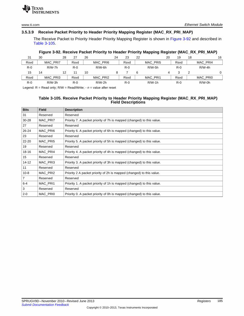
www.ti.com Ethernet Switch Module
185SPRUGV9D–November 2010–Revised June 2013Submit Documentation Feedback
Copyright © 2010–2013, Texas Instruments Incorporated
Registers
3.5.3.9 Receive Packet Priority to Header Priority Mapping Register (MAC_RX_PRI_MAP)The Receive Packet to Priority Header Priority Mapping Register is shown in Figure 3-92 and described inTable 3-105.
Figure 3-92. Receive Packet Priority to Header Priority Mapping Register (MAC_RX_PRI_MAP)31 30 28 27 26 24 23 22 20 19 18 16
Rsvd MAC_PRI7 Rsvd MAC_PRI6 Rsvd MAC_PRI5 Rsvd MAC_PRI4R-0 R/W-7h R-0 R/W-6h R-0 R/W-5h R-0 R/W-4h15 14 12 11 10 8 7 6 4 3 2 0
Rsvd MAC_PRI3 Rsvd MAC_PRI2 Rsvd MAC_PRI1 Rsvd MAC_PRI0R-0 R/W-3h R-0 R/W-2h R-0 R/W-1h R-0 R/W-0h
Legend: R = Read only; R/W = Read/Write; - n = value after reset
Table 3-105. Receive Packet Priority to Header Priority Mapping Register (MAC_RX_PRI_MAP)Field Descriptions
Bits Field Description31 Reserved Reserved30-28 MAC_PRI7 Priority 7. A packet priority of 7h is mapped (changed) to this value.27 Reserved Reserved26-24 MAC_PRI6 Priority 6. A packet priority of 6h is mapped (changed) to this value.23 Reserved Reserved22-20 MAC_PRI5 Priority 5. A packet priority of 5h is mapped (changed) to this value.19 Reserved Reserved18-16 MAC_PRI4 Priority 4. A packet priority of 4h is mapped (changed) to this value.15 Reserved Reserved14-12 MAC_PRI3 Priority 3. A packet priority of 3h is mapped (changed) to this value.11 Reserved Reserved10-8 MAC_PRI2 Priority 2 A packet priority of 2h is mapped (changed) to this value.7 Reserved Reserved6-4 MAC_PRI1 Priority 1. A packet priority of 1h is mapped (changed) to this value.3 Reserved Reserved2-0 MAC_PRI0 Priority 0. A packet priority of 0h is mapped (changed) to this value.
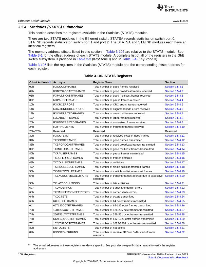
Ethernet Switch Module www.ti.com
186 SPRUGV9D–November 2010–Revised June 2013Submit Documentation Feedback
Copyright © 2010–2013, Texas Instruments Incorporated
Registers
3.5.4 Statistics (STATS) SubmoduleThis section describes the registers available in the Statistics (STATS) modules.
There are two STATS modules in the Ethernet switch. STATSA records statistics on switch port 0.STATSB records statistics on switch port 1 and port 2. The STATSA and STATSB modules each have anidentical registers.
The memory address offsets listed in this section in Table 3-106 are relative to the STATS module. SeeTable 3-1 for the offset address of each STATS module. A complete list of all of the registers in the GbEswitch subsystem is provided in Table 3-3 (KeyStone I) and in Table 3-4 (KeyStone II).
Table 3-106 lists the registers in the Statistics (STATS) module and the corresponding offset address foreach register.
(1) The actual addresses of these registers are device specific. See your device-specific data manual to verify the registeraddresses.
Table 3-106. STATS Registers
Offset Address (1) Acronym Register Name Section00h RXGOODFRAMES Total number of good frames received Section 3.5.4.104h RXBROADCASTFRAMES Total number of good broadcast frames received Section 3.5.4.208h RXMULTICASTFRAMES Total number of good multicast frames received Section 3.5.4.30Ch RXPAUSEFRAMES Total number of pause frames received Section 3.5.4.410h RXCRCERRORS Total number of CRC errors frames received Section 3.5.4.514h RXALIGNCODEERRORS Total number of alignment/code errors received Section 3.5.4.618h RXOVERSIZEDFRAMES Total number of oversized frames received Section 3.5.4.71Ch RXJABBERFRAMES Total number of jabber frames received Section 3.5.4.820h RXUNDERSIZEDFRAMES Total number of undersized frames received Section 3.5.4.924h RXFRAGMENTS Total number of fragment frames received Section 3.5.4.1028h-32Fh Reserved Reserved Reserved30h RXOCTETS Total number of received bytes in good frames Section 3.5.4.1134h TXGOODFRAMES Total number of good frames transmitted Section 3.5.4.1238h TXBROADCASTFRAMES Total number of good broadcast frames transmitted Section 3.5.4.133Ch TXMULTICASTFRAMES Total number of good multicast frames transmitted Section 3.5.4.1440h TXPAUSEFRAMES Total number of pause frames transmitted Section 3.5.4.1544h TXDEFERREDFRAMES Total number of frames deferred Section 3.5.4.1648h TXCOLLISIONFRAMES Total number of collisions Section 3.5.4.174Ch TXSINGLECOLLFRAMES Total number of single collision transmit frames Section 3.5.4.1850h TXMULTCOLLFRAMES Total number of multiple collision transmit frames Section 3.5.4.1954h TXEXCESSIVECOLLISIONS Total number of transmit frames aborted due to excessive
collisionsSection 3.5.4.20
58h TXLATECOLLISIONS Total number of late collisions Section 3.5.4.215Ch TXUNDERRUN Total number of transmit underrun errors Section 3.5.4.2260h TXCARRIERSENSEERRORS Total number of carrier sense errors Section 3.5.4.2364h TXOCTETS Total number of octets transmitted Section 3.5.4.2468h 64OCTETFRAMES Total number of 64 octet frames transmitted Section 3.5.4.256Ch 65T127OCTETFRAMES Total number of 65-127 octet frames transmitted Section 3.5.4.2670h 128T255OCTETFRAMES Total number of 128-255 octet frames transmitted Section 3.5.4.2774h 256T511OCTETFRAMES Total number of 256-511 octet frames transmitted Section 3.5.4.2878h 512T1023OCTETFRAMES Total number of 512-1023 octet frames transmitted Section 3.5.4.297Ch 1024TUPOCTETFRAMES Total number of 1023-1518 octet frames transmitted Section 3.5.4.3080h NETOCTETS Total number of net octets Section 3.5.4.3184h RXSOFOVERRUNS Total number of receive FIFO or DMA start of frame
overrunsSection 3.5.4.32
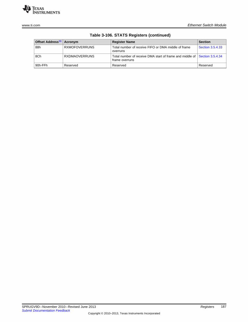
www.ti.com Ethernet Switch Module
187SPRUGV9D–November 2010–Revised June 2013Submit Documentation Feedback
Copyright © 2010–2013, Texas Instruments Incorporated
Registers
Table 3-106. STATS Registers (continued)Offset Address (1) Acronym Register Name Section88h RXMOFOVERRUNS Total number of receive FIFO or DMA middle of frame
overrunsSection 3.5.4.33
8Ch RXDMAOVERRUNS Total number of receive DMA start of frame and middle offrame overruns
Section 3.5.4.34
90h-FFh Reserved Reserved Reserved
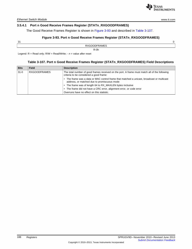
Ethernet Switch Module www.ti.com
188 SPRUGV9D–November 2010–Revised June 2013Submit Documentation Feedback
Copyright © 2010–2013, Texas Instruments Incorporated
Registers
3.5.4.1 Port n Good Receive Frames Register (STATn_RXGOODFRAMES)The Good Receive Frames Register is shown in Figure 3-93 and described in Table 3-107.
Figure 3-93. Port n Good Receive Frames Register (STATn_RXGOODFRAMES)31 0
RXGOODFRAMESR-0h
Legend: R = Read only; R/W = Read/Write; - n = value after reset
Table 3-107. Port n Good Receive Frames Register (STATn_RXGOODFRAMES) Field Descriptions
Bits Field Description31-0 RXGOODFRAMES The total number of good frames received on the port. A frame must match all of the following
criteria to be considered a good frame:• The frame was a data or MAC control frame that matched a unicast, broadcast or multicast
address, or matched due to promiscuous mode• The frame was of length 64 to RX_MAXLEN bytes inclusive• The frame did not have a CRC error, alignment error, or code errorOverruns have no effect on this statistic.
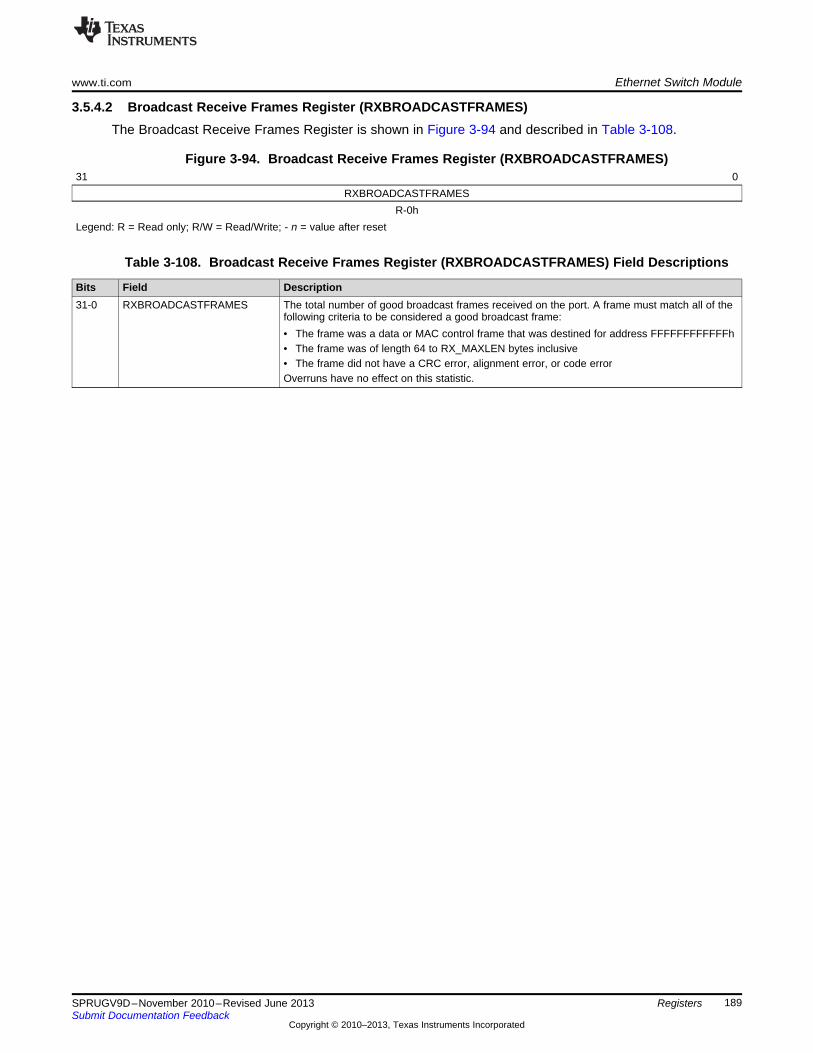
www.ti.com Ethernet Switch Module
189SPRUGV9D–November 2010–Revised June 2013Submit Documentation Feedback
Copyright © 2010–2013, Texas Instruments Incorporated
Registers
3.5.4.2 Broadcast Receive Frames Register (RXBROADCASTFRAMES)The Broadcast Receive Frames Register is shown in Figure 3-94 and described in Table 3-108.
Figure 3-94. Broadcast Receive Frames Register (RXBROADCASTFRAMES)31 0
RXBROADCASTFRAMESR-0h
Legend: R = Read only; R/W = Read/Write; - n = value after reset
Table 3-108. Broadcast Receive Frames Register (RXBROADCASTFRAMES) Field Descriptions
Bits Field Description31-0 RXBROADCASTFRAMES The total number of good broadcast frames received on the port. A frame must match all of the
following criteria to be considered a good broadcast frame:• The frame was a data or MAC control frame that was destined for address FFFFFFFFFFFFh• The frame was of length 64 to RX_MAXLEN bytes inclusive• The frame did not have a CRC error, alignment error, or code errorOverruns have no effect on this statistic.
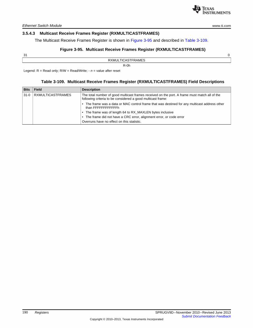
Ethernet Switch Module www.ti.com
190 SPRUGV9D–November 2010–Revised June 2013Submit Documentation Feedback
Copyright © 2010–2013, Texas Instruments Incorporated
Registers
3.5.4.3 Multicast Receive Frames Register (RXMULTICASTFRAMES)The Multicast Receive Frames Register is shown in Figure 3-95 and described in Table 3-109.
Figure 3-95. Multicast Receive Frames Register (RXMULTICASTFRAMES)31 0
RXMULTICASTFRAMESR-0h
Legend: R = Read only; R/W = Read/Write; - n = value after reset
Table 3-109. Multicast Receive Frames Register (RXMULTICASTFRAMES) Field Descriptions
Bits Field Description31-0 RXMULTICASTFRAMES The total number of good multicast frames received on the port. A frame must match all of the
following criteria to be considered a good multicast frame:• The frame was a data or MAC control frame that was destined for any multicast address other
than FFFFFFFFFFFFh• The frame was of length 64 to RX_MAXLEN bytes inclusive• The frame did not have a CRC error, alignment error, or code errorOverruns have no effect on this statistic.
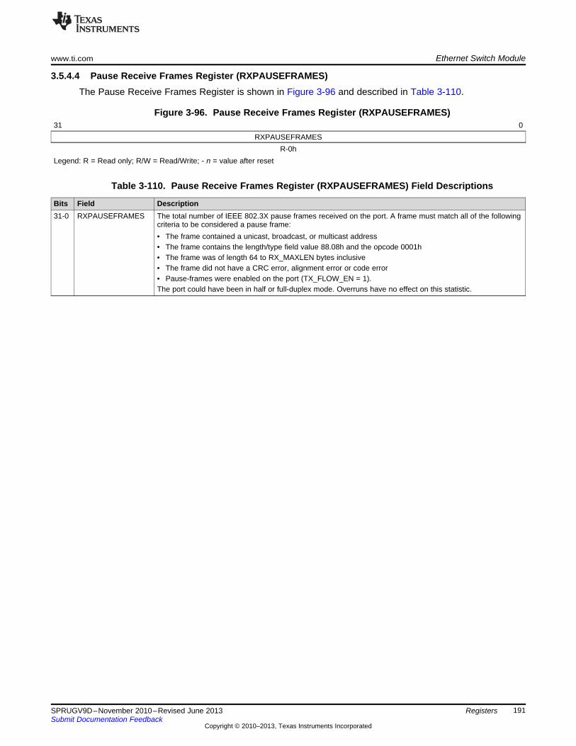
www.ti.com Ethernet Switch Module
191SPRUGV9D–November 2010–Revised June 2013Submit Documentation Feedback
Copyright © 2010–2013, Texas Instruments Incorporated
Registers
3.5.4.4 Pause Receive Frames Register (RXPAUSEFRAMES)The Pause Receive Frames Register is shown in Figure 3-96 and described in Table 3-110.
Figure 3-96. Pause Receive Frames Register (RXPAUSEFRAMES)31 0
RXPAUSEFRAMESR-0h
Legend: R = Read only; R/W = Read/Write; - n = value after reset
Table 3-110. Pause Receive Frames Register (RXPAUSEFRAMES) Field Descriptions
Bits Field Description31-0 RXPAUSEFRAMES The total number of IEEE 802.3X pause frames received on the port. A frame must match all of the following
criteria to be considered a pause frame:• The frame contained a unicast, broadcast, or multicast address• The frame contains the length/type field value 88.08h and the opcode 0001h• The frame was of length 64 to RX_MAXLEN bytes inclusive• The frame did not have a CRC error, alignment error or code error• Pause-frames were enabled on the port (TX_FLOW_EN = 1).The port could have been in half or full-duplex mode. Overruns have no effect on this statistic.
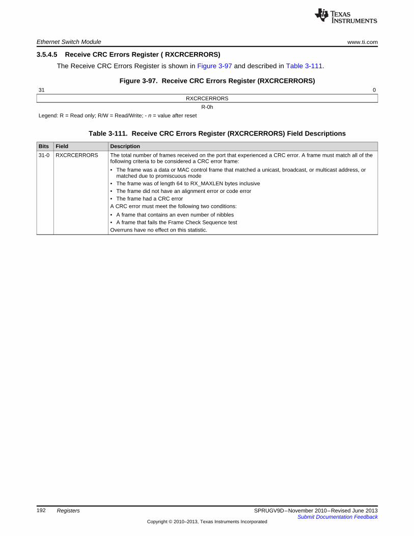
Ethernet Switch Module www.ti.com
192 SPRUGV9D–November 2010–Revised June 2013Submit Documentation Feedback
Copyright © 2010–2013, Texas Instruments Incorporated
Registers
3.5.4.5 Receive CRC Errors Register ( RXCRCERRORS)The Receive CRC Errors Register is shown in Figure 3-97 and described in Table 3-111.
Figure 3-97. Receive CRC Errors Register (RXCRCERRORS)31 0
RXCRCERRORSR-0h
Legend: R = Read only; R/W = Read/Write; - n = value after reset
Table 3-111. Receive CRC Errors Register (RXCRCERRORS) Field Descriptions
Bits Field Description31-0 RXCRCERRORS The total number of frames received on the port that experienced a CRC error. A frame must match all of the
following criteria to be considered a CRC error frame:• The frame was a data or MAC control frame that matched a unicast, broadcast, or multicast address, or
matched due to promiscuous mode• The frame was of length 64 to RX_MAXLEN bytes inclusive• The frame did not have an alignment error or code error• The frame had a CRC errorA CRC error must meet the following two conditions:• A frame that contains an even number of nibbles• A frame that fails the Frame Check Sequence testOverruns have no effect on this statistic.
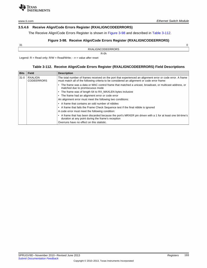
www.ti.com Ethernet Switch Module
193SPRUGV9D–November 2010–Revised June 2013Submit Documentation Feedback
Copyright © 2010–2013, Texas Instruments Incorporated
Registers
3.5.4.6 Receive Align/Code Errors Register (RXALIGNCODEERRORS)The Receive Align/Code Errors Register is shown in Figure 3-98 and described in Table 3-112.
Figure 3-98. Receive Align/Code Errors Register (RXALIGNCODEERRORS)31 0
RXALIGNCODEERRORSR-0h
Legend: R = Read only; R/W = Read/Write; - n = value after reset
Table 3-112. Receive Align/Code Errors Register (RXALIGNCODEERRORS) Field Descriptions
Bits Field Description31-0 RXALIGN
CODEERRORSThe total number of frames received on the port that experienced an alignment error or code error. A framemust match all of the following criteria to be considered an alignment or code error frame:• The frame was a data or MAC control frame that matched a unicast, broadcast, or multicast address, or
matched due to promiscuous mode• The frame was of length 64 to RX_MAXLEN bytes inclusive• The frame had an alignment error or code errorAn alignment error must meet the following two conditions:• A frame that contains an odd number of nibbles• A frame that fails the Frame Check Sequence test if the final nibble is ignoredA code error must meet the following condition:• A frame that has been discarded because the port’s MRXER pin driven with a 1 for at least one bit-time’s
duration at any point during the frame’s receptionOverruns have no effect on this statistic.
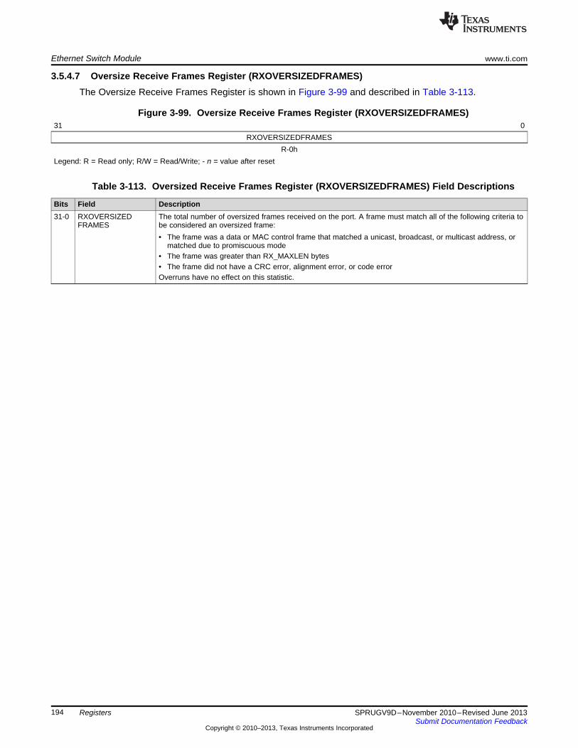
Ethernet Switch Module www.ti.com
194 SPRUGV9D–November 2010–Revised June 2013Submit Documentation Feedback
Copyright © 2010–2013, Texas Instruments Incorporated
Registers
3.5.4.7 Oversize Receive Frames Register (RXOVERSIZEDFRAMES)The Oversize Receive Frames Register is shown in Figure 3-99 and described in Table 3-113.
Figure 3-99. Oversize Receive Frames Register (RXOVERSIZEDFRAMES)31 0
RXOVERSIZEDFRAMESR-0h
Legend: R = Read only; R/W = Read/Write; - n = value after reset
Table 3-113. Oversized Receive Frames Register (RXOVERSIZEDFRAMES) Field Descriptions
Bits Field Description31-0 RXOVERSIZED
FRAMESThe total number of oversized frames received on the port. A frame must match all of the following criteria tobe considered an oversized frame:• The frame was a data or MAC control frame that matched a unicast, broadcast, or multicast address, or
matched due to promiscuous mode• The frame was greater than RX_MAXLEN bytes• The frame did not have a CRC error, alignment error, or code errorOverruns have no effect on this statistic.
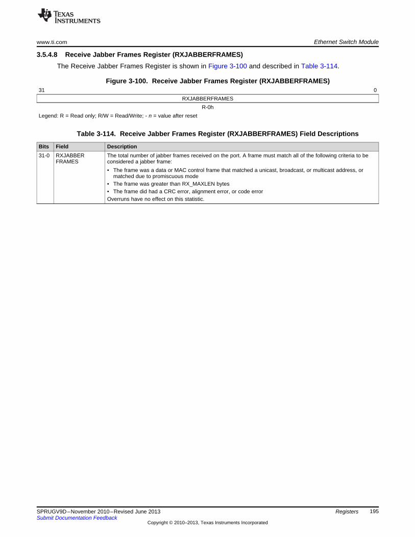
www.ti.com Ethernet Switch Module
195SPRUGV9D–November 2010–Revised June 2013Submit Documentation Feedback
Copyright © 2010–2013, Texas Instruments Incorporated
Registers
3.5.4.8 Receive Jabber Frames Register (RXJABBERFRAMES)The Receive Jabber Frames Register is shown in Figure 3-100 and described in Table 3-114.
Figure 3-100. Receive Jabber Frames Register (RXJABBERFRAMES)31 0
RXJABBERFRAMESR-0h
Legend: R = Read only; R/W = Read/Write; - n = value after reset
Table 3-114. Receive Jabber Frames Register (RXJABBERFRAMES) Field Descriptions
Bits Field Description31-0 RXJABBER
FRAMESThe total number of jabber frames received on the port. A frame must match all of the following criteria to beconsidered a jabber frame:• The frame was a data or MAC control frame that matched a unicast, broadcast, or multicast address, or
matched due to promiscuous mode• The frame was greater than RX_MAXLEN bytes• The frame did had a CRC error, alignment error, or code errorOverruns have no effect on this statistic.
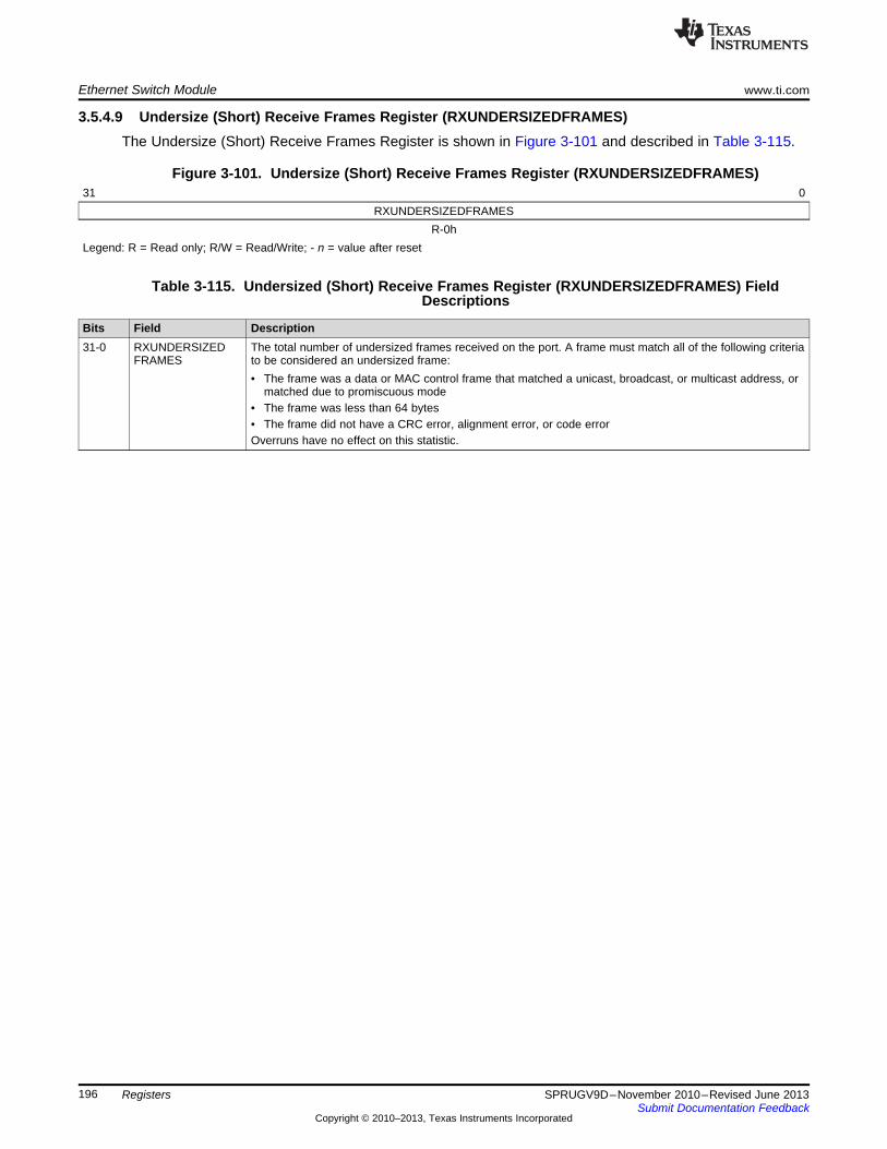
Ethernet Switch Module www.ti.com
196 SPRUGV9D–November 2010–Revised June 2013Submit Documentation Feedback
Copyright © 2010–2013, Texas Instruments Incorporated
Registers
3.5.4.9 Undersize (Short) Receive Frames Register (RXUNDERSIZEDFRAMES)The Undersize (Short) Receive Frames Register is shown in Figure 3-101 and described in Table 3-115.
Figure 3-101. Undersize (Short) Receive Frames Register (RXUNDERSIZEDFRAMES)31 0
RXUNDERSIZEDFRAMESR-0h
Legend: R = Read only; R/W = Read/Write; - n = value after reset
Table 3-115. Undersized (Short) Receive Frames Register (RXUNDERSIZEDFRAMES) FieldDescriptions
Bits Field Description31-0 RXUNDERSIZED
FRAMESThe total number of undersized frames received on the port. A frame must match all of the following criteriato be considered an undersized frame:• The frame was a data or MAC control frame that matched a unicast, broadcast, or multicast address, or
matched due to promiscuous mode• The frame was less than 64 bytes• The frame did not have a CRC error, alignment error, or code errorOverruns have no effect on this statistic.
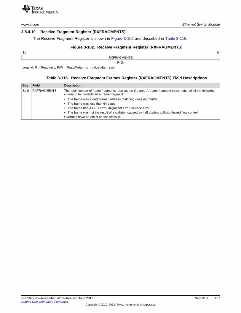
www.ti.com Ethernet Switch Module
197SPRUGV9D–November 2010–Revised June 2013Submit Documentation Feedback
Copyright © 2010–2013, Texas Instruments Incorporated
Registers
3.5.4.10 Receive Fragment Register (RXFRAGMENTS)The Receive Fragment Register is shown in Figure 3-102 and described in Table 3-116.
Figure 3-102. Receive Fragment Register (RXFRAGMENTS)31 0
RXFRAGMENTSR-0h
Legend: R = Read only; R/W = Read/Write; - n = value after reset
Table 3-116. Receive Fragment Frames Register (RXFRAGMENTS) Field Descriptions
Bits Field Description31-0 RXFRAGMENTS The total number of frame fragments received on the port. A frame fragment must match all of the following
criteria to be considered a frame fragment:• The frame was a data frame (address matching does not matter)• The frame was less than 64 bytes• The frame had a CRC error, alignment error, or code error• The frame was not the result of a collision caused by half duplex, collision based flow controlOverruns have no effect on this statistic.
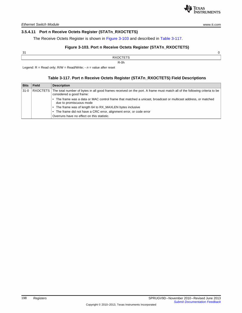
Ethernet Switch Module www.ti.com
198 SPRUGV9D–November 2010–Revised June 2013Submit Documentation Feedback
Copyright © 2010–2013, Texas Instruments Incorporated
Registers
3.5.4.11 Port n Receive Octets Register (STATn_RXOCTETS)The Receive Octets Register is shown in Figure 3-103 and described in Table 3-117.
Figure 3-103. Port n Receive Octets Register (STATn_RXOCTETS)31 0
RXOCTETSR-0h
Legend: R = Read only; R/W = Read/Write; - n = value after reset
Table 3-117. Port n Receive Octets Register (STATn_RXOCTETS) Field Descriptions
Bits Field Description31-0 RXOCTETS The total number of bytes in all good frames received on the port. A frame must match all of the following criteria to be
considered a good frame:• The frame was a data or MAC control frame that matched a unicast, broadcast or multicast address, or matched
due to promiscuous mode• The frame was of length 64 to RX_MAXLEN bytes inclusive• The frame did not have a CRC error, alignment error, or code errorOverruns have no effect on this statistic.
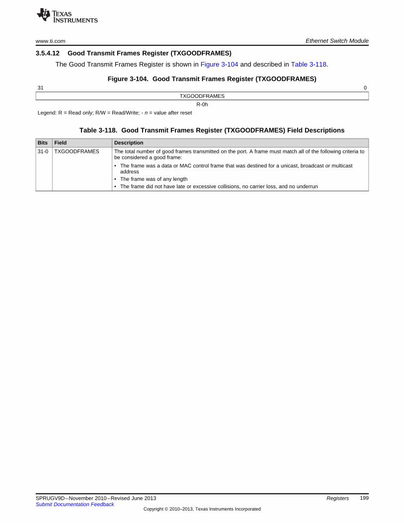
www.ti.com Ethernet Switch Module
199SPRUGV9D–November 2010–Revised June 2013Submit Documentation Feedback
Copyright © 2010–2013, Texas Instruments Incorporated
Registers
3.5.4.12 Good Transmit Frames Register (TXGOODFRAMES)The Good Transmit Frames Register is shown in Figure 3-104 and described in Table 3-118.
Figure 3-104. Good Transmit Frames Register (TXGOODFRAMES)31 0
TXGOODFRAMESR-0h
Legend: R = Read only; R/W = Read/Write; - n = value after reset
Table 3-118. Good Transmit Frames Register (TXGOODFRAMES) Field Descriptions
Bits Field Description31-0 TXGOODFRAMES The total number of good frames transmitted on the port. A frame must match all of the following criteria to
be considered a good frame:• The frame was a data or MAC control frame that was destined for a unicast, broadcast or multicast
address• The frame was of any length• The frame did not have late or excessive collisions, no carrier loss, and no underrun
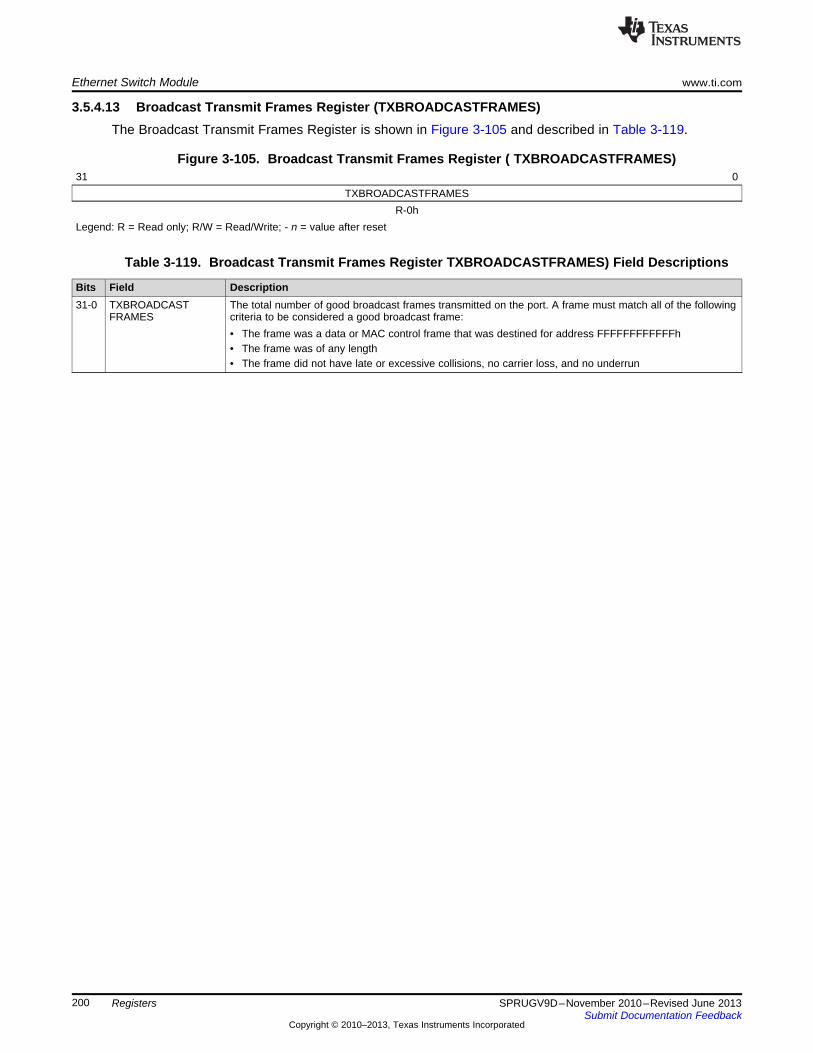
Ethernet Switch Module www.ti.com
200 SPRUGV9D–November 2010–Revised June 2013Submit Documentation Feedback
Copyright © 2010–2013, Texas Instruments Incorporated
Registers
3.5.4.13 Broadcast Transmit Frames Register (TXBROADCASTFRAMES)The Broadcast Transmit Frames Register is shown in Figure 3-105 and described in Table 3-119.
Figure 3-105. Broadcast Transmit Frames Register ( TXBROADCASTFRAMES)31 0
TXBROADCASTFRAMESR-0h
Legend: R = Read only; R/W = Read/Write; - n = value after reset
Table 3-119. Broadcast Transmit Frames Register TXBROADCASTFRAMES) Field Descriptions
Bits Field Description31-0 TXBROADCAST
FRAMESThe total number of good broadcast frames transmitted on the port. A frame must match all of the followingcriteria to be considered a good broadcast frame:• The frame was a data or MAC control frame that was destined for address FFFFFFFFFFFFh• The frame was of any length• The frame did not have late or excessive collisions, no carrier loss, and no underrun
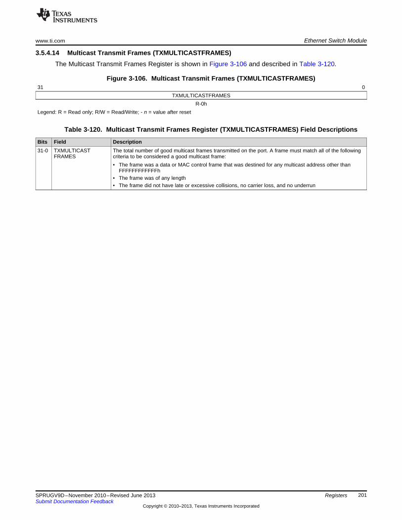
www.ti.com Ethernet Switch Module
201SPRUGV9D–November 2010–Revised June 2013Submit Documentation Feedback
Copyright © 2010–2013, Texas Instruments Incorporated
Registers
3.5.4.14 Multicast Transmit Frames (TXMULTICASTFRAMES)The Multicast Transmit Frames Register is shown in Figure 3-106 and described in Table 3-120.
Figure 3-106. Multicast Transmit Frames (TXMULTICASTFRAMES)31 0
TXMULTICASTFRAMESR-0h
Legend: R = Read only; R/W = Read/Write; - n = value after reset
Table 3-120. Multicast Transmit Frames Register (TXMULTICASTFRAMES) Field Descriptions
Bits Field Description31-0 TXMULTICAST
FRAMESThe total number of good multicast frames transmitted on the port. A frame must match all of the followingcriteria to be considered a good multicast frame:• The frame was a data or MAC control frame that was destined for any multicast address other than
FFFFFFFFFFFFh• The frame was of any length• The frame did not have late or excessive collisions, no carrier loss, and no underrun
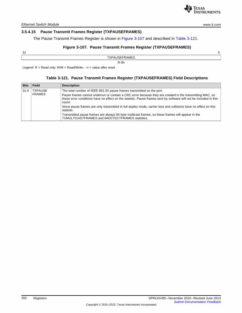
Ethernet Switch Module www.ti.com
202 SPRUGV9D–November 2010–Revised June 2013Submit Documentation Feedback
Copyright © 2010–2013, Texas Instruments Incorporated
Registers
3.5.4.15 Pause Transmit Frames Register (TXPAUSEFRAMES)The Pause Transmit Frames Register is shown in Figure 3-107 and described in Table 3-121.
Figure 3-107. Pause Transmit Frames Register (TXPAUSEFRAMES)31 0
TXPAUSEFRAMESR-0h
Legend: R = Read only; R/W = Read/Write; - n = value after reset
Table 3-121. Pause Transmit Frames Register (TXPAUSEFRAMES) Field Descriptions
Bits Field Description31-0 TXPAUSE
FRAMESThe total number of IEEE 802.3X pause frames transmitted on the port.Pause frames cannot underrun or contain a CRC error because they are created in the transmitting MAC, sothese error conditions have no effect on the statistic. Pause frames sent by software will not be included in thiscount.Since pause frames are only transmitted in full duplex mode, carrier loss and collisions have no effect on thisstatistic.Transmitted pause frames are always 64 byte multicast frames, so these frames will appear in theTXMULTICASTFRAMES and 64OCTECTFRAMES statistics.
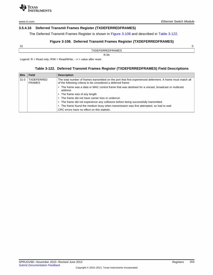
www.ti.com Ethernet Switch Module
203SPRUGV9D–November 2010–Revised June 2013Submit Documentation Feedback
Copyright © 2010–2013, Texas Instruments Incorporated
Registers
3.5.4.16 Deferred Transmit Frames Register (TXDEFERREDFRAMES)The Deferred Transmit Frames Register is shown in Figure 3-108 and described in Table 3-122.
Figure 3-108. Deferred Transmit Frames Register (TXDEFERREDFRAMES)31 0
TXDEFERREDFRAMESR-0h
Legend: R = Read only; R/W = Read/Write; - n = value after reset
Table 3-122. Deferred Transmit Frames Register (TXDEFERREDFRAMES) Field Descriptions
Bits Field Description31-0 TXDEFERRED
FRAMESThe total number of frames transmitted on the port that first experienced deferment. A frame must match allof the following criteria to be considered a deferred frame:• The frame was a data or MAC control frame that was destined for a unicast, broadcast or multicast
address• The frame was of any length• The frame did not have carrier loss or underrun• The frame did not experience any collisions before being successfully transmitted• The frame found the medium busy when transmission was first attempted, so had to waitCRC errors have no effect on this statistic.
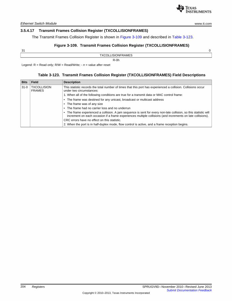
Ethernet Switch Module www.ti.com
204 SPRUGV9D–November 2010–Revised June 2013Submit Documentation Feedback
Copyright © 2010–2013, Texas Instruments Incorporated
Registers
3.5.4.17 Transmit Frames Collision Register (TXCOLLISIONFRAMES)The Transmit Frames Collision Register is shown in Figure 3-109 and described in Table 3-123.
Figure 3-109. Transmit Frames Collision Register (TXCOLLISIONFRAMES)31 0
TXCOLLISIONFRAMESR-0h
Legend: R = Read only; R/W = Read/Write; - n = value after reset
Table 3-123. Transmit Frames Collision Register (TXCOLLISIONFRAMES) Field Descriptions
Bits Field Description31-0 TXCOLLISION
FRAMESThis statistic records the total number of times that this port has experienced a collision. Collisions occurunder two circumstances:1. When all of the following conditions are true for a transmit data or MAC control frame:• The frame was destined for any unicast, broadcast or multicast address• The frame was of any size• The frame had no carrier loss and no underrun• The frame experienced a collision. A jam sequence is sent for every non-late collision, so this statistic will
increment on each occasion if a frame experiences multiple collisions (and increments on late collisions).CRC errors have no effect on this statistic.2. When the port is in half-duplex mode, flow control is active, and a frame reception begins.
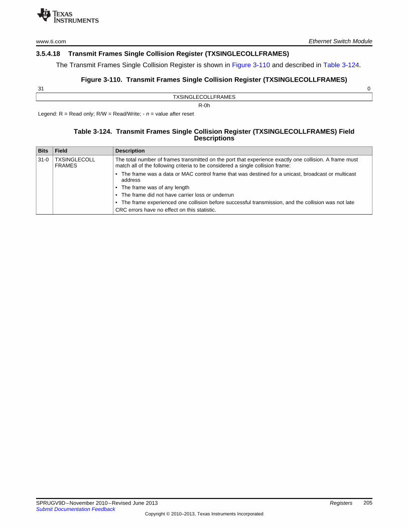
www.ti.com Ethernet Switch Module
205SPRUGV9D–November 2010–Revised June 2013Submit Documentation Feedback
Copyright © 2010–2013, Texas Instruments Incorporated
Registers
3.5.4.18 Transmit Frames Single Collision Register (TXSINGLECOLLFRAMES)The Transmit Frames Single Collision Register is shown in Figure 3-110 and described in Table 3-124.
Figure 3-110. Transmit Frames Single Collision Register (TXSINGLECOLLFRAMES)31 0
TXSINGLECOLLFRAMESR-0h
Legend: R = Read only; R/W = Read/Write; - n = value after reset
Table 3-124. Transmit Frames Single Collision Register (TXSINGLECOLLFRAMES) FieldDescriptions
Bits Field Description31-0 TXSINGLECOLL
FRAMESThe total number of frames transmitted on the port that experience exactly one collision. A frame mustmatch all of the following criteria to be considered a single collision frame:• The frame was a data or MAC control frame that was destined for a unicast, broadcast or multicast
address• The frame was of any length• The frame did not have carrier loss or underrun• The frame experienced one collision before successful transmission, and the collision was not lateCRC errors have no effect on this statistic.
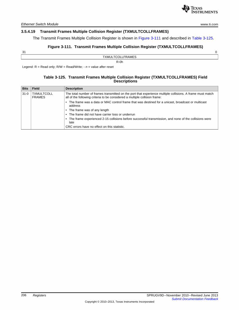
Ethernet Switch Module www.ti.com
206 SPRUGV9D–November 2010–Revised June 2013Submit Documentation Feedback
Copyright © 2010–2013, Texas Instruments Incorporated
Registers
3.5.4.19 Transmit Frames Multiple Collision Register (TXMULTCOLLFRAMES)The Transmit Frames Multiple Collision Register is shown in Figure 3-111 and described in Table 3-125.
Figure 3-111. Transmit Frames Multiple Collision Register (TXMULTCOLLFRAMES)31 0
TXMULTCOLLFRAMESR-0h
Legend: R = Read only; R/W = Read/Write; - n = value after reset
Table 3-125. Transmit Frames Multiple Collision Register (TXMULTCOLLFRAMES) FieldDescriptions
Bits Field Description31-0 TXMULTCOLL
FRAMESThe total number of frames transmitted on the port that experience multiple collisions. A frame must matchall of the following criteria to be considered a multiple collision frame:• The frame was a data or MAC control frame that was destined for a unicast, broadcast or multicast
address• The frame was of any length• The frame did not have carrier loss or underrun• The frame experienced 2-15 collisions before successful transmission, and none of the collisions were
lateCRC errors have no effect on this statistic.
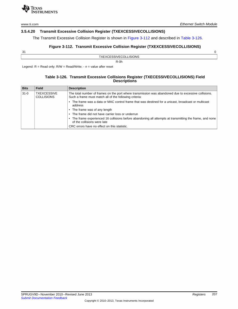
www.ti.com Ethernet Switch Module
207SPRUGV9D–November 2010–Revised June 2013Submit Documentation Feedback
Copyright © 2010–2013, Texas Instruments Incorporated
Registers
3.5.4.20 Transmit Excessive Collision Register (TXEXCESSIVECOLLISIONS)The Transmit Excessive Collision Register is shown in Figure 3-112 and described in Table 3-126.
Figure 3-112. Transmit Excessive Collision Register (TXEXCESSIVECOLLISIONS)31 0
TXEXCESSIVECOLLISIONSR-0h
Legend: R = Read only; R/W = Read/Write; - n = value after reset
Table 3-126. Transmit Excessive Collisions Register (TXECESSIVECOLLISIONS) FieldDescriptions
Bits Field Description31-0 TXEXCESSIVE
COLLISIONSThe total number of frames on the port where transmission was abandoned due to excessive collisions.Such a frame must match all of the following criteria:• The frame was a data or MAC control frame that was destined for a unicast, broadcast or multicast
address• The frame was of any length• The frame did not have carrier loss or underrun• The frame experienced 16 collisions before abandoning all attempts at transmitting the frame, and none
of the collisions were lateCRC errors have no effect on this statistic.
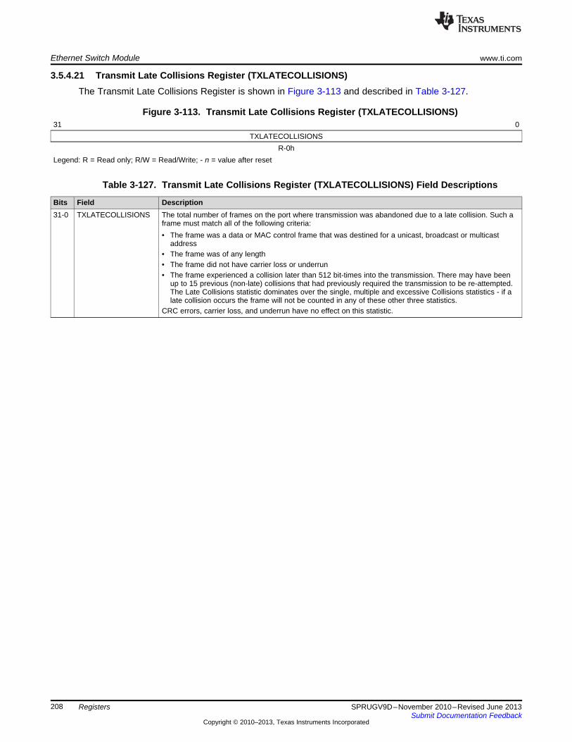
Ethernet Switch Module www.ti.com
208 SPRUGV9D–November 2010–Revised June 2013Submit Documentation Feedback
Copyright © 2010–2013, Texas Instruments Incorporated
Registers
3.5.4.21 Transmit Late Collisions Register (TXLATECOLLISIONS)The Transmit Late Collisions Register is shown in Figure 3-113 and described in Table 3-127.
Figure 3-113. Transmit Late Collisions Register (TXLATECOLLISIONS)31 0
TXLATECOLLISIONSR-0h
Legend: R = Read only; R/W = Read/Write; - n = value after reset
Table 3-127. Transmit Late Collisions Register (TXLATECOLLISIONS) Field Descriptions
Bits Field Description31-0 TXLATECOLLISIONS The total number of frames on the port where transmission was abandoned due to a late collision. Such a
frame must match all of the following criteria:• The frame was a data or MAC control frame that was destined for a unicast, broadcast or multicast
address• The frame was of any length• The frame did not have carrier loss or underrun• The frame experienced a collision later than 512 bit-times into the transmission. There may have been
up to 15 previous (non-late) collisions that had previously required the transmission to be re-attempted.The Late Collisions statistic dominates over the single, multiple and excessive Collisions statistics - if alate collision occurs the frame will not be counted in any of these other three statistics.
CRC errors, carrier loss, and underrun have no effect on this statistic.
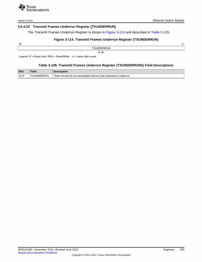
www.ti.com Ethernet Switch Module
209SPRUGV9D–November 2010–Revised June 2013Submit Documentation Feedback
Copyright © 2010–2013, Texas Instruments Incorporated
Registers
3.5.4.22 Transmit Frames Underrun Register (TXUNDERRUN)The Transmit Frames Underrun Register is shown in Figure 3-114 and described in Table 3-128.
Figure 3-114. Transmit Frames Underrun Register (TXUNDERRUN)31 0
TXUNDERRUNR-0h
Legend: R = Read only; R/W = Read/Write; - n = value after reset
Table 3-128. Transmit Frames Underrun Register (TXUNDERRUNS) Field Descriptions
Bits Field Description31-0 TXUNDERRUN There should be no transmitted frames that experience underrun.
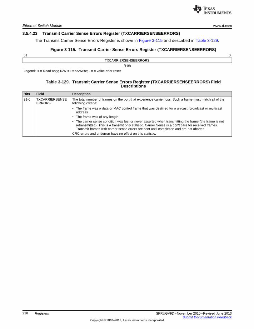
Ethernet Switch Module www.ti.com
210 SPRUGV9D–November 2010–Revised June 2013Submit Documentation Feedback
Copyright © 2010–2013, Texas Instruments Incorporated
Registers
3.5.4.23 Transmit Carrier Sense Errors Register (TXCARRIERSENSEERRORS)The Transmit Carrier Sense Errors Register is shown in Figure 3-115 and described in Table 3-129.
Figure 3-115. Transmit Carrier Sense Errors Register (TXCARRIERSENSEERRORS)31 0
TXCARRIERSENSEERRORSR-0h
Legend: R = Read only; R/W = Read/Write; - n = value after reset
Table 3-129. Transmit Carrier Sense Errors Register (TXCARRIERSENSEERRORS) FieldDescriptions
Bits Field Description31-0 TXCARRIERSENSE
ERRORSThe total number of frames on the port that experience carrier loss. Such a frame must match all of thefollowing criteria:• The frame was a data or MAC control frame that was destined for a unicast, broadcast or multicast
address• The frame was of any length• The carrier sense condition was lost or never asserted when transmitting the frame (the frame is not
retransmitted). This is a transmit only statistic. Carrier Sense is a don't care for received frames.Transmit frames with carrier sense errors are sent until completion and are not aborted.
CRC errors and underrun have no effect on this statistic.
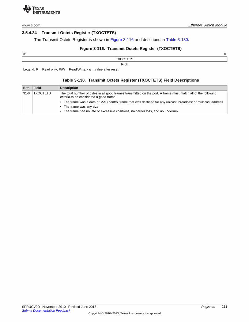
www.ti.com Ethernet Switch Module
211SPRUGV9D–November 2010–Revised June 2013Submit Documentation Feedback
Copyright © 2010–2013, Texas Instruments Incorporated
Registers
3.5.4.24 Transmit Octets Register (TXOCTETS)The Transmit Octets Register is shown in Figure 3-116 and described in Table 3-130.
Figure 3-116. Transmit Octets Register (TXOCTETS)31 0
TXOCTETSR-0h
Legend: R = Read only; R/W = Read/Write; - n = value after reset
Table 3-130. Transmit Octets Register (TXOCTETS) Field Descriptions
Bits Field Description31-0 TXOCTETS The total number of bytes in all good frames transmitted on the port. A frame must match all of the following
criteria to be considered a good frame:• The frame was a data or MAC control frame that was destined for any unicast, broadcast or multicast address• The frame was any size• The frame had no late or excessive collisions, no carrier loss, and no underrun
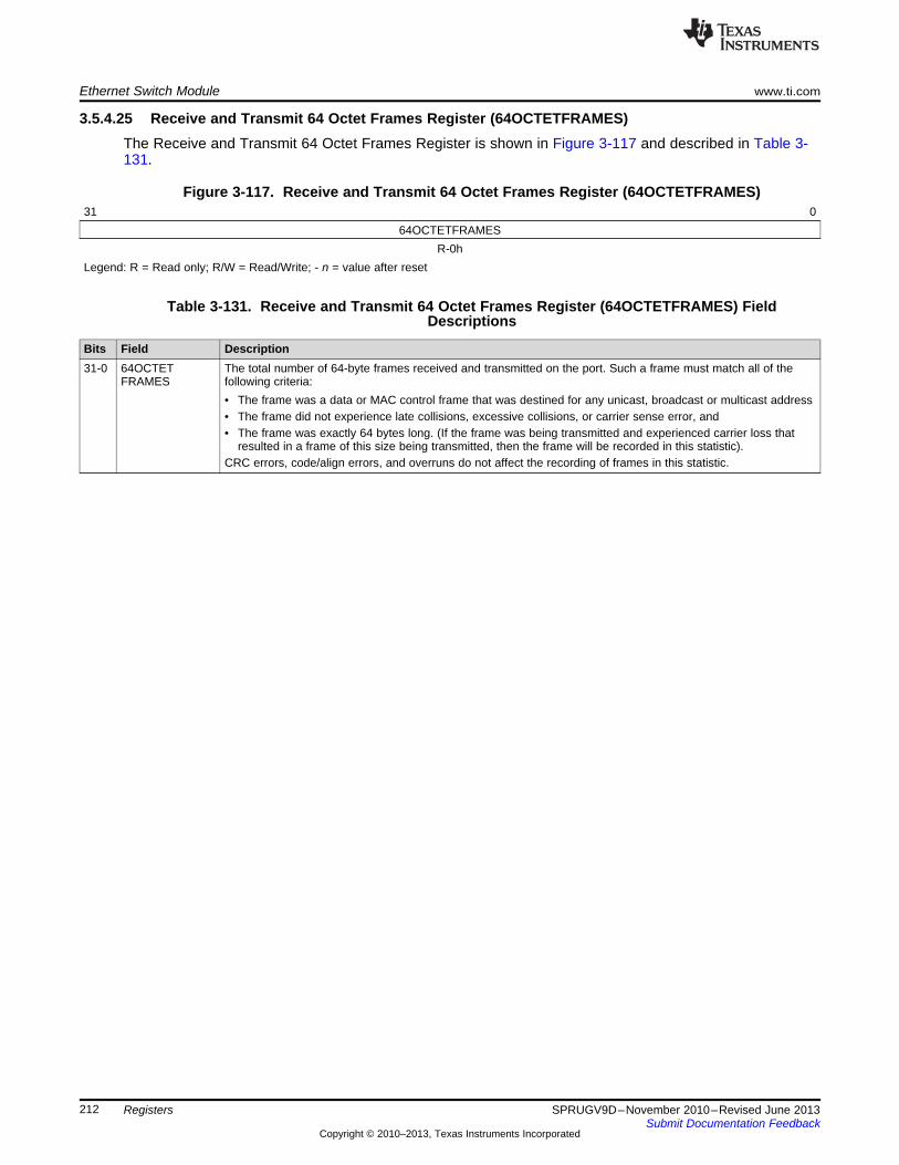
Ethernet Switch Module www.ti.com
212 SPRUGV9D–November 2010–Revised June 2013Submit Documentation Feedback
Copyright © 2010–2013, Texas Instruments Incorporated
Registers
3.5.4.25 Receive and Transmit 64 Octet Frames Register (64OCTETFRAMES)The Receive and Transmit 64 Octet Frames Register is shown in Figure 3-117 and described in Table 3-131.
Figure 3-117. Receive and Transmit 64 Octet Frames Register (64OCTETFRAMES)31 0
64OCTETFRAMESR-0h
Legend: R = Read only; R/W = Read/Write; - n = value after reset
Table 3-131. Receive and Transmit 64 Octet Frames Register (64OCTETFRAMES) FieldDescriptions
Bits Field Description31-0 64OCTET
FRAMESThe total number of 64-byte frames received and transmitted on the port. Such a frame must match all of thefollowing criteria:• The frame was a data or MAC control frame that was destined for any unicast, broadcast or multicast address• The frame did not experience late collisions, excessive collisions, or carrier sense error, and• The frame was exactly 64 bytes long. (If the frame was being transmitted and experienced carrier loss that
resulted in a frame of this size being transmitted, then the frame will be recorded in this statistic).CRC errors, code/align errors, and overruns do not affect the recording of frames in this statistic.
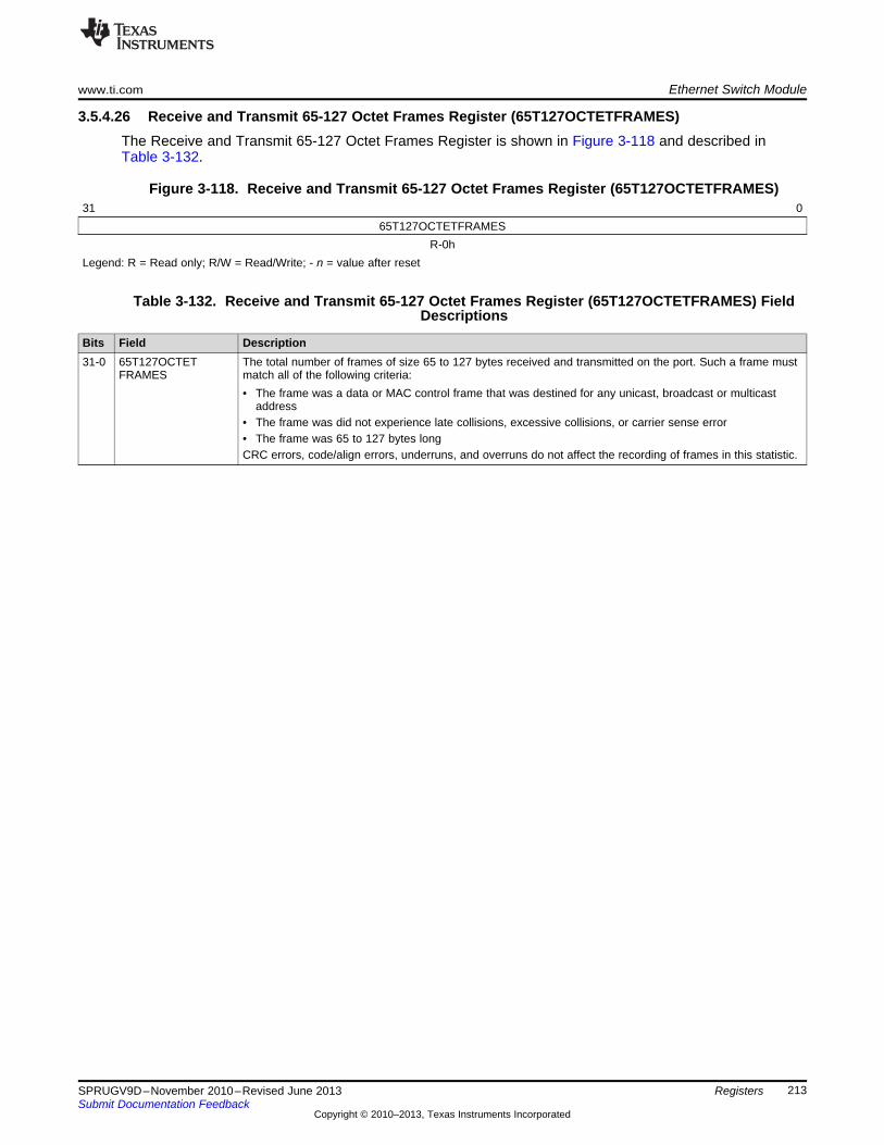
www.ti.com Ethernet Switch Module
213SPRUGV9D–November 2010–Revised June 2013Submit Documentation Feedback
Copyright © 2010–2013, Texas Instruments Incorporated
Registers
3.5.4.26 Receive and Transmit 65-127 Octet Frames Register (65T127OCTETFRAMES)The Receive and Transmit 65-127 Octet Frames Register is shown in Figure 3-118 and described inTable 3-132.
Figure 3-118. Receive and Transmit 65-127 Octet Frames Register (65T127OCTETFRAMES)31 0
65T127OCTETFRAMESR-0h
Legend: R = Read only; R/W = Read/Write; - n = value after reset
Table 3-132. Receive and Transmit 65-127 Octet Frames Register (65T127OCTETFRAMES) FieldDescriptions
Bits Field Description31-0 65T127OCTET
FRAMESThe total number of frames of size 65 to 127 bytes received and transmitted on the port. Such a frame mustmatch all of the following criteria:• The frame was a data or MAC control frame that was destined for any unicast, broadcast or multicast
address• The frame was did not experience late collisions, excessive collisions, or carrier sense error• The frame was 65 to 127 bytes longCRC errors, code/align errors, underruns, and overruns do not affect the recording of frames in this statistic.
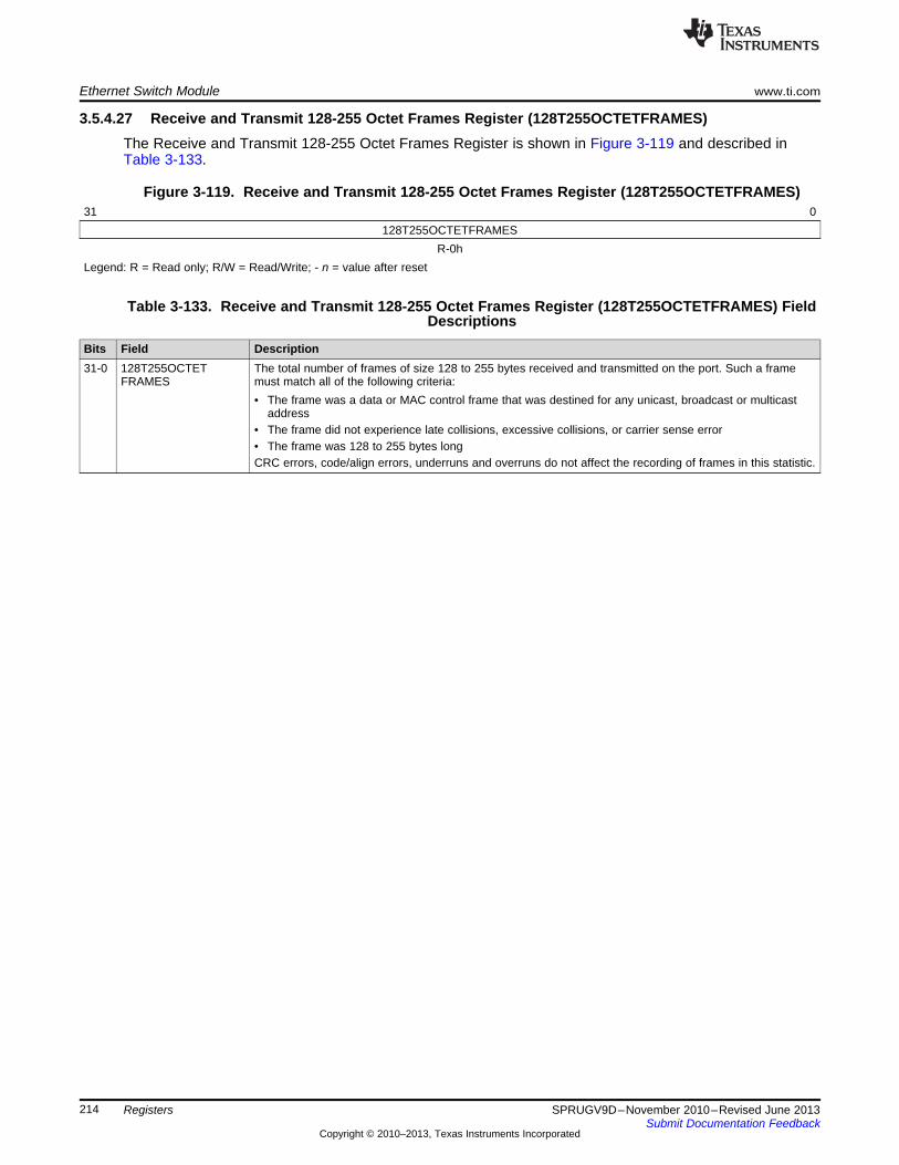
Ethernet Switch Module www.ti.com
214 SPRUGV9D–November 2010–Revised June 2013Submit Documentation Feedback
Copyright © 2010–2013, Texas Instruments Incorporated
Registers
3.5.4.27 Receive and Transmit 128-255 Octet Frames Register (128T255OCTETFRAMES)The Receive and Transmit 128-255 Octet Frames Register is shown in Figure 3-119 and described inTable 3-133.
Figure 3-119. Receive and Transmit 128-255 Octet Frames Register (128T255OCTETFRAMES)31 0
128T255OCTETFRAMESR-0h
Legend: R = Read only; R/W = Read/Write; - n = value after reset
Table 3-133. Receive and Transmit 128-255 Octet Frames Register (128T255OCTETFRAMES) FieldDescriptions
Bits Field Description31-0 128T255OCTET
FRAMESThe total number of frames of size 128 to 255 bytes received and transmitted on the port. Such a framemust match all of the following criteria:• The frame was a data or MAC control frame that was destined for any unicast, broadcast or multicast
address• The frame did not experience late collisions, excessive collisions, or carrier sense error• The frame was 128 to 255 bytes longCRC errors, code/align errors, underruns and overruns do not affect the recording of frames in this statistic.

www.ti.com Ethernet Switch Module
215SPRUGV9D–November 2010–Revised June 2013Submit Documentation Feedback
Copyright © 2010–2013, Texas Instruments Incorporated
Registers
3.5.4.28 Receive and Transmit 256-511 Octet Frames Register (256T511OCTETFRAMES)The Receive and Transmit 256-511 Octet Frames Register is shown in Figure 3-120 and described inTable 3-134.
Figure 3-120. Receive and Transmit 256-511 Octet Frames Register (256T511OCTETFRAMES)31 0
256T511OCTETFRAMESR-0h
Legend: R = Read only; R/W = Read/Write; - n = value after reset
Table 3-134. Receive and Transmit 256-511 Octet Frames Register (256T511OCTETFRAMES) FieldDescriptions
Bits Field Description31-0 256T511OCTET
FRAMESThe total number of frames of size 256 to 511 bytes received and transmitted on the port. Such a framemust match all of the following criteria:• The frame was a data or MAC control frame that was destined for any unicast, broadcast or multicast
address• The frame did not experience late collisions, excessive collisions, or carrier sense error• The frame was 256 to 511 bytes longCRC errors, code/align errors, underruns and overruns do not affect the recording of frames in this statistic.
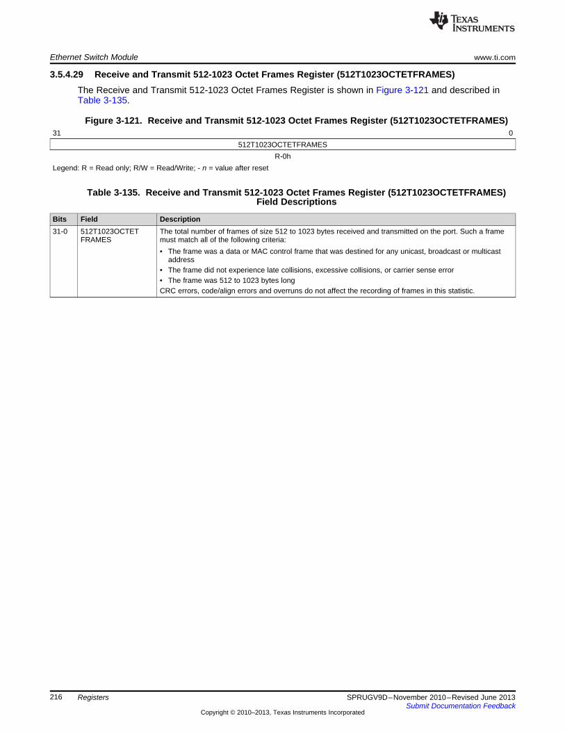
Ethernet Switch Module www.ti.com
216 SPRUGV9D–November 2010–Revised June 2013Submit Documentation Feedback
Copyright © 2010–2013, Texas Instruments Incorporated
Registers
3.5.4.29 Receive and Transmit 512-1023 Octet Frames Register (512T1023OCTETFRAMES)The Receive and Transmit 512-1023 Octet Frames Register is shown in Figure 3-121 and described inTable 3-135.
Figure 3-121. Receive and Transmit 512-1023 Octet Frames Register (512T1023OCTETFRAMES)31 0
512T1023OCTETFRAMESR-0h
Legend: R = Read only; R/W = Read/Write; - n = value after reset
Table 3-135. Receive and Transmit 512-1023 Octet Frames Register (512T1023OCTETFRAMES)Field Descriptions
Bits Field Description31-0 512T1023OCTET
FRAMESThe total number of frames of size 512 to 1023 bytes received and transmitted on the port. Such a framemust match all of the following criteria:• The frame was a data or MAC control frame that was destined for any unicast, broadcast or multicast
address• The frame did not experience late collisions, excessive collisions, or carrier sense error• The frame was 512 to 1023 bytes longCRC errors, code/align errors and overruns do not affect the recording of frames in this statistic.
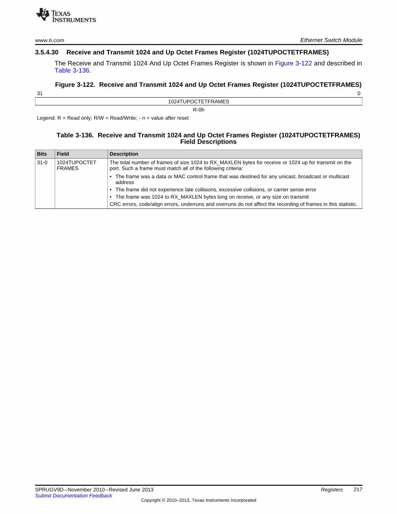
www.ti.com Ethernet Switch Module
217SPRUGV9D–November 2010–Revised June 2013Submit Documentation Feedback
Copyright © 2010–2013, Texas Instruments Incorporated
Registers
3.5.4.30 Receive and Transmit 1024 and Up Octet Frames Register (1024TUPOCTETFRAMES)The Receive and Transmit 1024 And Up Octet Frames Register is shown in Figure 3-122 and described inTable 3-136.
Figure 3-122. Receive and Transmit 1024 and Up Octet Frames Register (1024TUPOCTETFRAMES)31 0
1024TUPOCTETFRAMESR-0h
Legend: R = Read only; R/W = Read/Write; - n = value after reset
Table 3-136. Receive and Transmit 1024 and Up Octet Frames Register (1024TUPOCTETFRAMES)Field Descriptions
Bits Field Description31-0 1024TUPOCTET
FRAMESThe total number of frames of size 1024 to RX_MAXLEN bytes for receive or 1024 up for transmit on theport. Such a frame must match all of the following criteria:• The frame was a data or MAC control frame that was destined for any unicast, broadcast or multicast
address• The frame did not experience late collisions, excessive collisions, or carrier sense error• The frame was 1024 to RX_MAXLEN bytes long on receive, or any size on transmitCRC errors, code/align errors, underruns and overruns do not affect the recording of frames in this statistic.
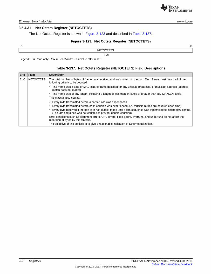
Ethernet Switch Module www.ti.com
218 SPRUGV9D–November 2010–Revised June 2013Submit Documentation Feedback
Copyright © 2010–2013, Texas Instruments Incorporated
Registers
3.5.4.31 Net Octets Register (NETOCTETS)The Net Octets Register is shown in Figure 3-123 and described in Table 3-137.
Figure 3-123. Net Octets Register (NETOCTETS)31 0
NETOCTETSR-0h
Legend: R = Read only; R/W = Read/Write; - n = value after reset
Table 3-137. Net Octets Register (NETOCTETS) Field Descriptions
Bits Field Description31-0 NETOCTETS The total number of bytes of frame data received and transmitted on the port. Each frame must match all of the
following criteria to be counted:• The frame was a data or MAC control frame destined for any unicast, broadcast, or multicast address (address
match does not matter)• The frame was of any length, including a length of less than 64 bytes or greater than RX_MAXLEN bytesThis statistic also counts:• Every byte transmitted before a carrier-loss was experienced• Every byte transmitted before each collision was experienced (i.e. multiple retries are counted each time)• Every byte received if the port is in half-duplex mode until a jam sequence was transmitted to initiate flow control.
(The jam sequence was not counted to prevent double-counting).Error conditions such as alignment errors, CRC errors, code errors, overruns, and underruns do not affect therecording of bytes by this statistic.The objective of this statistic is to give a reasonable indication of Ethernet utilization.
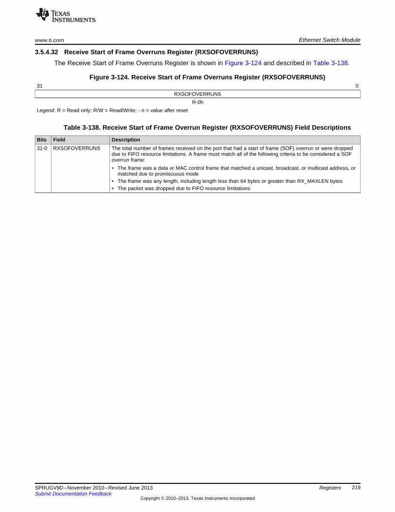
www.ti.com Ethernet Switch Module
219SPRUGV9D–November 2010–Revised June 2013Submit Documentation Feedback
Copyright © 2010–2013, Texas Instruments Incorporated
Registers
3.5.4.32 Receive Start of Frame Overruns Register (RXSOFOVERRUNS)The Receive Start of Frame Overruns Register is shown in Figure 3-124 and described in Table 3-138.
Figure 3-124. Receive Start of Frame Overruns Register (RXSOFOVERRUNS)31 0
RXSOFOVERRUNSR-0h
Legend: R = Read only; R/W = Read/Write; - n = value after reset
Table 3-138. Receive Start of Frame Overrun Register (RXSOFOVERRUNS) Field Descriptions
Bits Field Description31-0 RXSOFOVERRUNS The total number of frames received on the port that had a start of frame (SOF) overrun or were dropped
due to FIFO resource limitations. A frame must match all of the following criteria to be considered a SOFoverrun frame:• The frame was a data or MAC control frame that matched a unicast, broadcast, or multicast address, or
matched due to promiscuous mode• The frame was any length, including length less than 64 bytes or greater than RX_MAXLEN bytes• The packet was dropped due to FIFO resource limitations
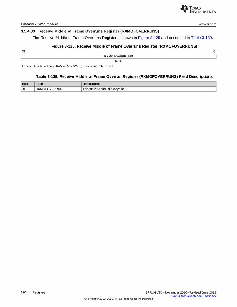
Ethernet Switch Module www.ti.com
220 SPRUGV9D–November 2010–Revised June 2013Submit Documentation Feedback
Copyright © 2010–2013, Texas Instruments Incorporated
Registers
3.5.4.33 Receive Middle of Frame Overruns Register (RXMOFOVERRUNS)The Receive Middle of Frame Overruns Register is shown in Figure 3-125 and described in Table 3-139.
Figure 3-125. Receive Middle of Frame Overruns Register (RXMOFOVERRUNS)31 0
RXMOFOVERRUNSR-0h
Legend: R = Read only; R/W = Read/Write; - n = value after reset
Table 3-139. Receive Middle of Frame Overrun Register (RXMOFOVERRUNS) Field Descriptions
Bits Field Description31-0 RXMOFOVERRUNS This statistic should always be 0.
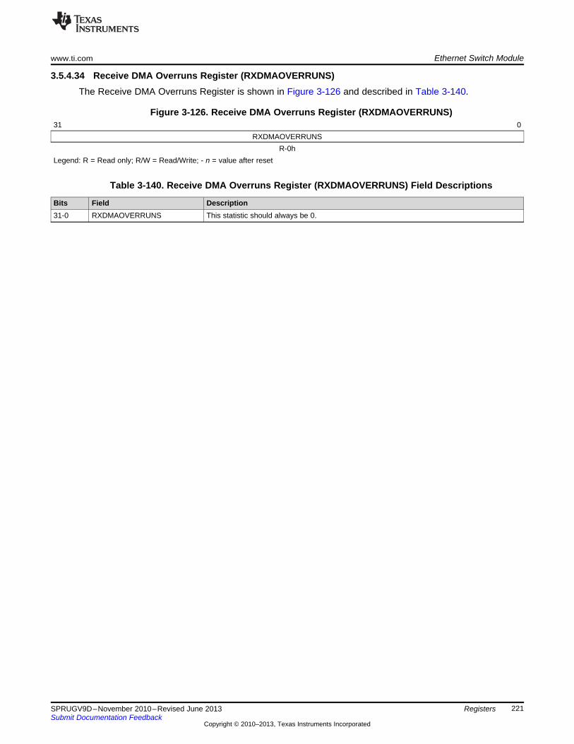
www.ti.com Ethernet Switch Module
221SPRUGV9D–November 2010–Revised June 2013Submit Documentation Feedback
Copyright © 2010–2013, Texas Instruments Incorporated
Registers
3.5.4.34 Receive DMA Overruns Register (RXDMAOVERRUNS)The Receive DMA Overruns Register is shown in Figure 3-126 and described in Table 3-140.
Figure 3-126. Receive DMA Overruns Register (RXDMAOVERRUNS)31 0
RXDMAOVERRUNSR-0h
Legend: R = Read only; R/W = Read/Write; - n = value after reset
Table 3-140. Receive DMA Overruns Register (RXDMAOVERRUNS) Field Descriptions
Bits Field Description31-0 RXDMAOVERRUNS This statistic should always be 0.
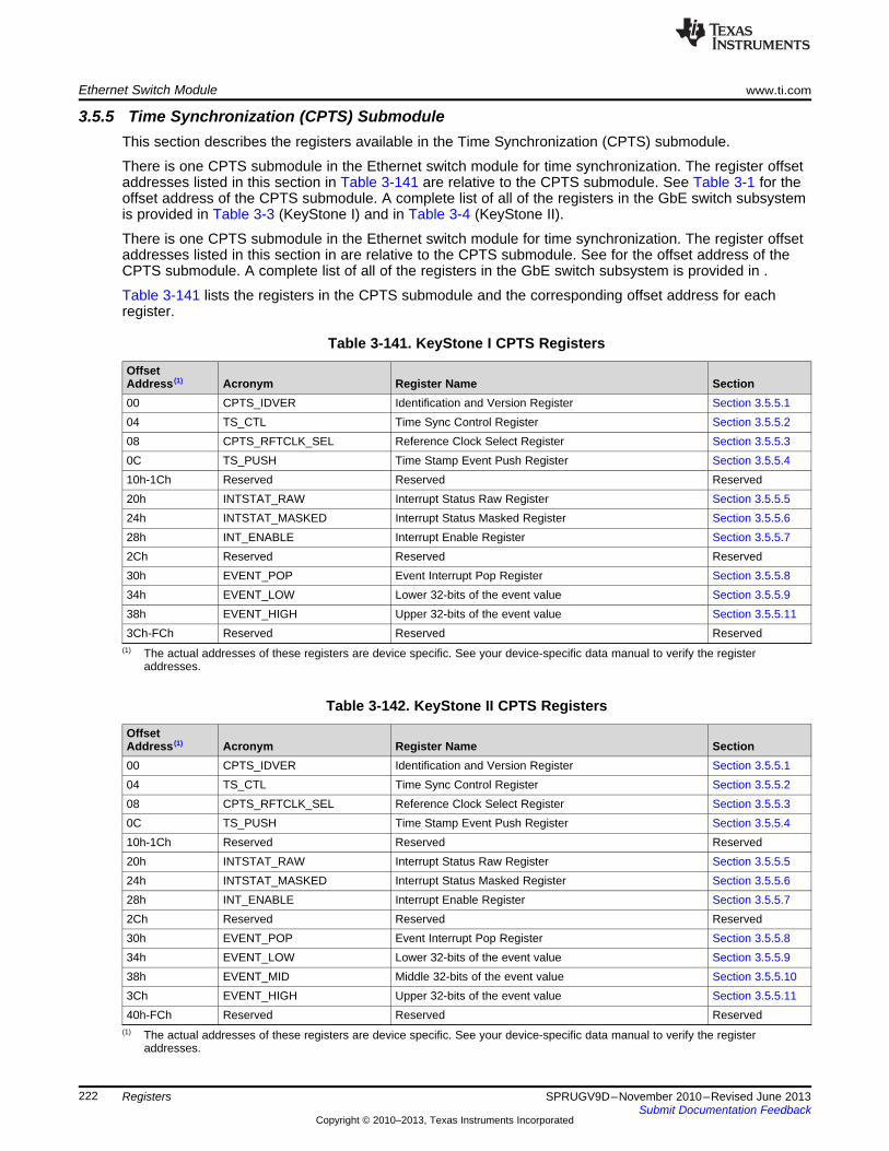
Ethernet Switch Module www.ti.com
222 SPRUGV9D–November 2010–Revised June 2013Submit Documentation Feedback
Copyright © 2010–2013, Texas Instruments Incorporated
Registers
3.5.5 Time Synchronization (CPTS) SubmoduleThis section describes the registers available in the Time Synchronization (CPTS) submodule.
There is one CPTS submodule in the Ethernet switch module for time synchronization. The register offsetaddresses listed in this section in Table 3-141 are relative to the CPTS submodule. See Table 3-1 for theoffset address of the CPTS submodule. A complete list of all of the registers in the GbE switch subsystemis provided in Table 3-3 (KeyStone I) and in Table 3-4 (KeyStone II).
There is one CPTS submodule in the Ethernet switch module for time synchronization. The register offsetaddresses listed in this section in are relative to the CPTS submodule. See for the offset address of theCPTS submodule. A complete list of all of the registers in the GbE switch subsystem is provided in .
Table 3-141 lists the registers in the CPTS submodule and the corresponding offset address for eachregister.
(1) The actual addresses of these registers are device specific. See your device-specific data manual to verify the registeraddresses.
Table 3-141. KeyStone I CPTS Registers
OffsetAddress (1) Acronym Register Name Section00 CPTS_IDVER Identification and Version Register Section 3.5.5.104 TS_CTL Time Sync Control Register Section 3.5.5.208 CPTS_RFTCLK_SEL Reference Clock Select Register Section 3.5.5.30C TS_PUSH Time Stamp Event Push Register Section 3.5.5.410h-1Ch Reserved Reserved Reserved20h INTSTAT_RAW Interrupt Status Raw Register Section 3.5.5.524h INTSTAT_MASKED Interrupt Status Masked Register Section 3.5.5.628h INT_ENABLE Interrupt Enable Register Section 3.5.5.72Ch Reserved Reserved Reserved30h EVENT_POP Event Interrupt Pop Register Section 3.5.5.834h EVENT_LOW Lower 32-bits of the event value Section 3.5.5.938h EVENT_HIGH Upper 32-bits of the event value Section 3.5.5.113Ch-FCh Reserved Reserved Reserved
(1) The actual addresses of these registers are device specific. See your device-specific data manual to verify the registeraddresses.
Table 3-142. KeyStone II CPTS Registers
OffsetAddress (1) Acronym Register Name Section00 CPTS_IDVER Identification and Version Register Section 3.5.5.104 TS_CTL Time Sync Control Register Section 3.5.5.208 CPTS_RFTCLK_SEL Reference Clock Select Register Section 3.5.5.30C TS_PUSH Time Stamp Event Push Register Section 3.5.5.410h-1Ch Reserved Reserved Reserved20h INTSTAT_RAW Interrupt Status Raw Register Section 3.5.5.524h INTSTAT_MASKED Interrupt Status Masked Register Section 3.5.5.628h INT_ENABLE Interrupt Enable Register Section 3.5.5.72Ch Reserved Reserved Reserved30h EVENT_POP Event Interrupt Pop Register Section 3.5.5.834h EVENT_LOW Lower 32-bits of the event value Section 3.5.5.938h EVENT_MID Middle 32-bits of the event value Section 3.5.5.103Ch EVENT_HIGH Upper 32-bits of the event value Section 3.5.5.1140h-FCh Reserved Reserved Reserved
www.ti.com Ethernet Switch Module
223SPRUGV9D–November 2010–Revised June 2013Submit Documentation Feedback
Copyright © 2010–2013, Texas Instruments Incorporated
Registers
3.5.5.1 CPTS Identification and Version Register (CPTS_IDVER)The CPTS Identification And Version Register is shown in Figure 3-127 and described in Table 3-143.
Figure 3-127. CPTS Identification and Version Register (CPTS_IDVER)31 16
CPTS_IDENTR-4E8Ah
15 11 10 8 7 0CPTS_RTL_VER CPTS_MAJOR_VER CPTS_MINOR_VER
R-0h R-0h R-2hLegend: R = Read only; R/W = Read/Write; - n = value after reset
Table 3-143. CPTS Identification and Version Register (CPTS_IDVER) Field Descriptions
Bits Field Description31-16 CPTS_IDENT CPTS Identification Value15-11 CPTS_RTL_VER RTL Version Value10-8 CPTS_MAJOR_VER Major Version Value7-0 CPTS_MINOR_VER Minor Version Value
Ethernet Switch Module www.ti.com
224 SPRUGV9D–November 2010–Revised June 2013Submit Documentation Feedback
Copyright © 2010–2013, Texas Instruments Incorporated
Registers
3.5.5.2 Time Sync Control Register (CPTS_CTL)The Time Sync Control Register is shown in Figure 3-128 and described in Table 3-144.
Figure 3-128. Time Sync Control Register (TS_CTL)31 1 0
Reserved CPTS_ENR-0h R/W-0h
Legend: R = Read only; R/W = Read/Write; - n = value after reset
Table 3-144. Time Sync Control Register (TS_CTL) Field Descriptions
Bits Field Description31-1 Reserved Reserved0 CPTS_EN Time Sync Enable. When disabled (cleared to 0), the RCLK domain is held in reset.
• 0 = Time Sync Disabled• 1 = Time Sync Enabled
www.ti.com Ethernet Switch Module
225SPRUGV9D–November 2010–Revised June 2013Submit Documentation Feedback
Copyright © 2010–2013, Texas Instruments Incorporated
Registers
3.5.5.3 RFTCLK Select Register (CPTS_RFTCLK_SEL)The CPTS_RFTCLK_SEL Select Register is shown in Figure 3-129 and described in Table 3-145.
Figure 3-129. RFTCLK Select Register (CPTS_RFTCLK_SEL)31 5 4 0
Reserved CPTS_RFTCLK_SELR-0h R/W-0h
Legend: R = Read only; R/W = Read/Write; - n = value after reset
Table 3-145. RFTCLK Select Register (CPTS_RFTCLK_SEL) Field Descriptions
Bits Field Description31-5 Reserved Reserved4-0 CPTS_RFTCLK_SEL Reference Clock Select. This signal is used to control an external multiplexer that selects one of up to
32 clocks for time sync reference (RFTCLK). This CPTS_RFTCLK_SEL value can be written only whenthe CPTS_EN bit is cleared to 0both the CPTS_EN and HR_EN bits are both cleared to 0 in theTS_CTL register. For more information on the clock sources for this module, please see the devicespecific data manual.
Ethernet Switch Module www.ti.com
226 SPRUGV9D–November 2010–Revised June 2013Submit Documentation Feedback
Copyright © 2010–2013, Texas Instruments Incorporated
Registers
3.5.5.4 Time Stamp Event Push Register (CPTS_TS_PUSH)The Time Stamp Event Push Register is shown in Figure 3-130 and described in Table 3-146.
Figure 3-130. Time Stamp Event Push Register (CPTS_TS_PUSH)31 1 0
Reserved TS_PUSH
R-0h R/W-0hLegend: R = Read only; R/W = Read/Write; - n = value after reset
Table 3-146. Time Stamp Event Push Register (CPTS_TS_PUSH) Field Descriptions
Bits Field Description31-1 Reserved Reserved0 TS_PUSH Time Stamp Event Push. When a logic high is written to this bit a time stamp event is pushed onto the event FIFO. The
time stamp value is the time of the write of this register, not the time of the event read. The time stamp value can thenbe read on interrupt via the event registers. Software should not push a second time stamp event onto the event FIFOuntil the first time stamp value has been read from the event FIFO (there should be only one time stamp event in theevent FIFO at any given time). This bit is write only and always reads 0.
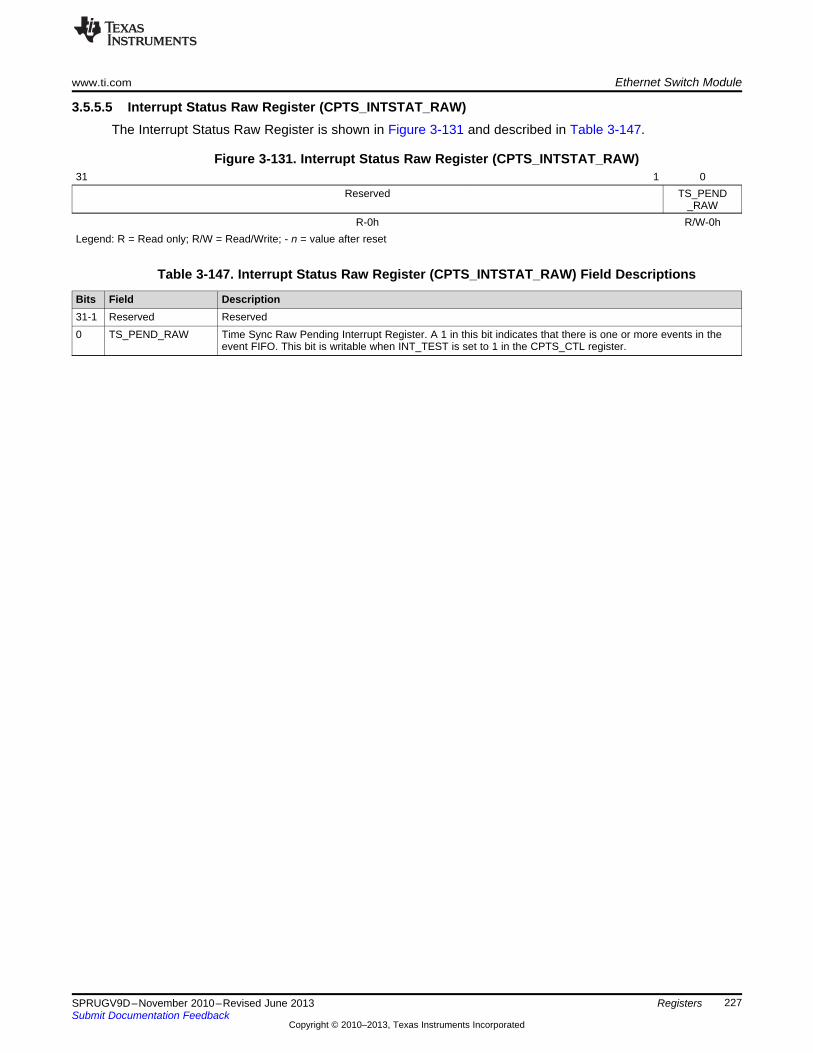
www.ti.com Ethernet Switch Module
227SPRUGV9D–November 2010–Revised June 2013Submit Documentation Feedback
Copyright © 2010–2013, Texas Instruments Incorporated
Registers
3.5.5.5 Interrupt Status Raw Register (CPTS_INTSTAT_RAW)The Interrupt Status Raw Register is shown in Figure 3-131 and described in Table 3-147.
Figure 3-131. Interrupt Status Raw Register (CPTS_INTSTAT_RAW)31 1 0
Reserved TS_PEND_RAW
R-0h R/W-0hLegend: R = Read only; R/W = Read/Write; - n = value after reset
Table 3-147. Interrupt Status Raw Register (CPTS_INTSTAT_RAW) Field Descriptions
Bits Field Description31-1 Reserved Reserved0 TS_PEND_RAW Time Sync Raw Pending Interrupt Register. A 1 in this bit indicates that there is one or more events in the
event FIFO. This bit is writable when INT_TEST is set to 1 in the CPTS_CTL register.
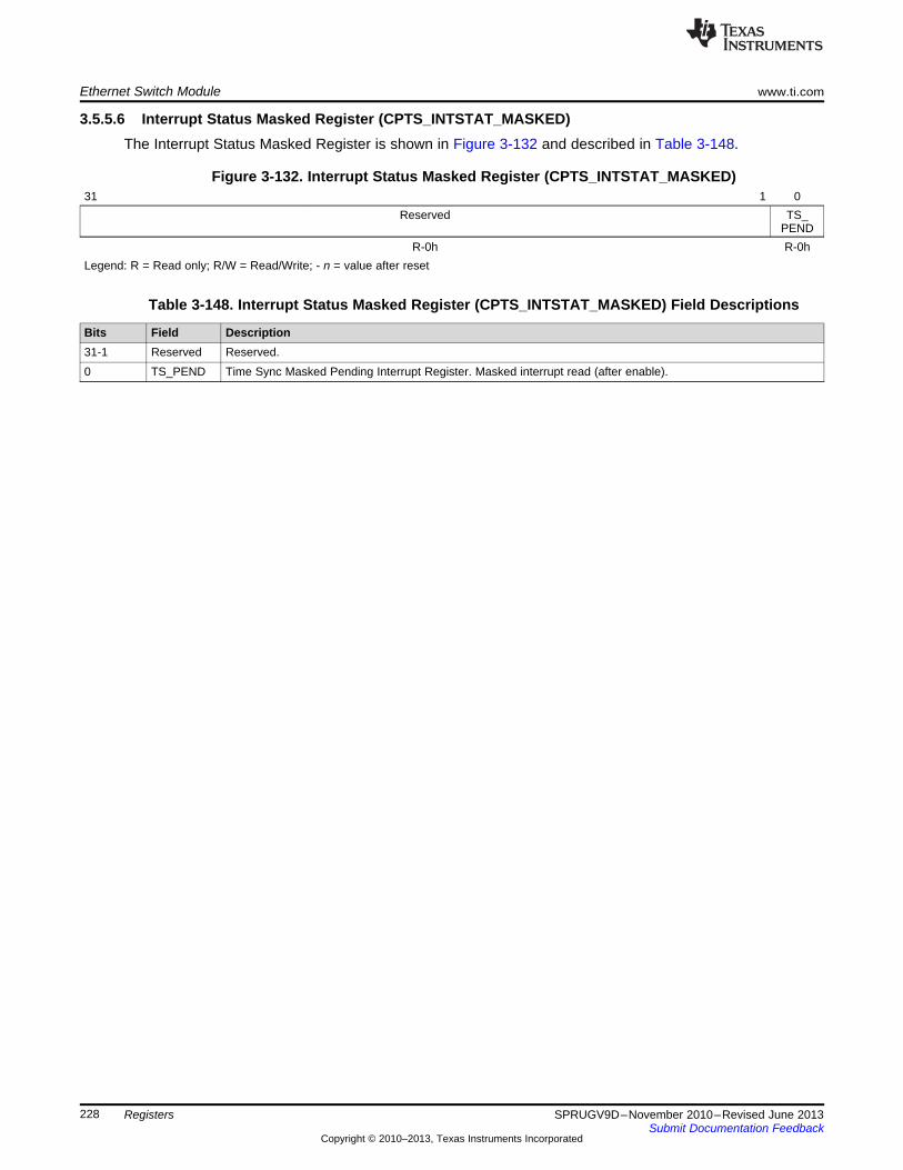
Ethernet Switch Module www.ti.com
228 SPRUGV9D–November 2010–Revised June 2013Submit Documentation Feedback
Copyright © 2010–2013, Texas Instruments Incorporated
Registers
3.5.5.6 Interrupt Status Masked Register (CPTS_INTSTAT_MASKED)The Interrupt Status Masked Register is shown in Figure 3-132 and described in Table 3-148.
Figure 3-132. Interrupt Status Masked Register (CPTS_INTSTAT_MASKED)31 1 0
Reserved TS_PEND
R-0h R-0hLegend: R = Read only; R/W = Read/Write; - n = value after reset
Table 3-148. Interrupt Status Masked Register (CPTS_INTSTAT_MASKED) Field Descriptions
Bits Field Description31-1 Reserved Reserved.0 TS_PEND Time Sync Masked Pending Interrupt Register. Masked interrupt read (after enable).
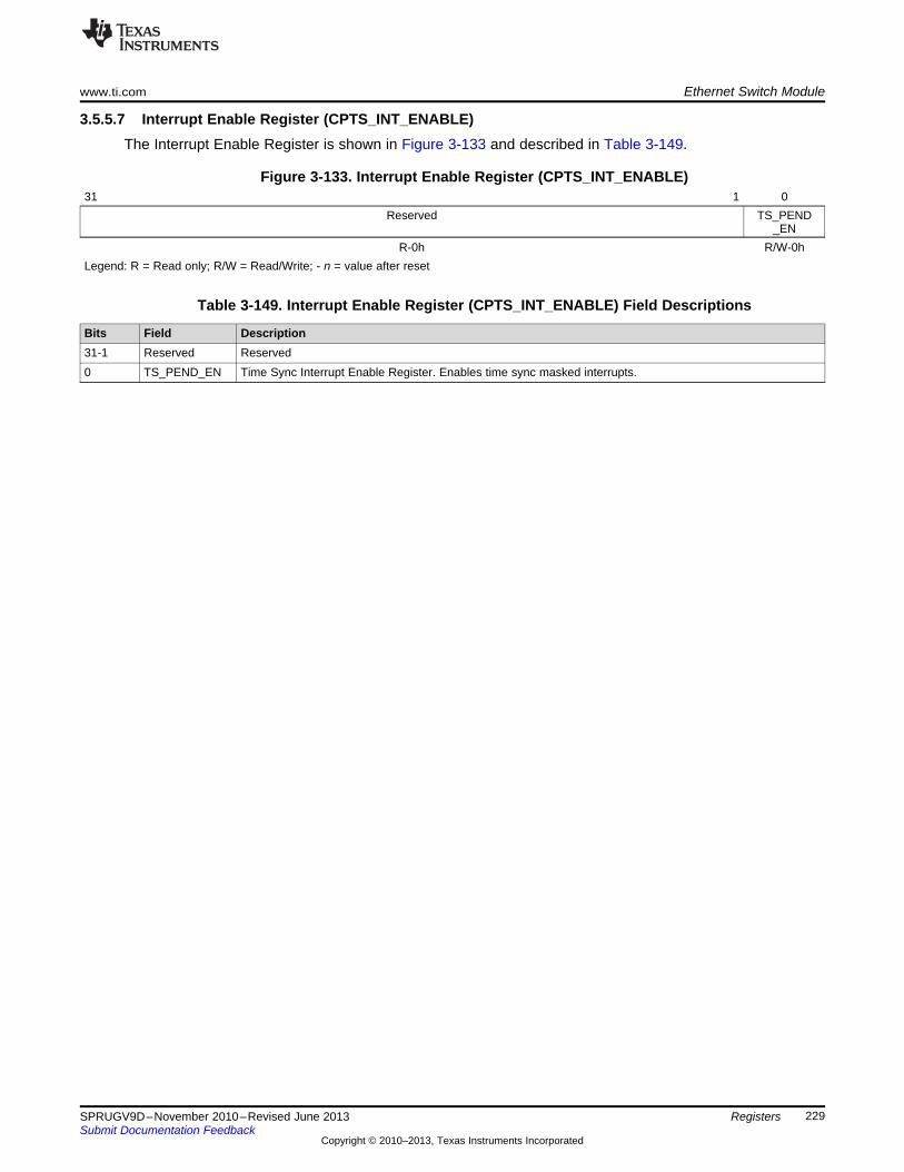
www.ti.com Ethernet Switch Module
229SPRUGV9D–November 2010–Revised June 2013Submit Documentation Feedback
Copyright © 2010–2013, Texas Instruments Incorporated
Registers
3.5.5.7 Interrupt Enable Register (CPTS_INT_ENABLE)The Interrupt Enable Register is shown in Figure 3-133 and described in Table 3-149.
Figure 3-133. Interrupt Enable Register (CPTS_INT_ENABLE)31 1 0
Reserved TS_PEND_EN
R-0h R/W-0hLegend: R = Read only; R/W = Read/Write; - n = value after reset
Table 3-149. Interrupt Enable Register (CPTS_INT_ENABLE) Field Descriptions
Bits Field Description31-1 Reserved Reserved0 TS_PEND_EN Time Sync Interrupt Enable Register. Enables time sync masked interrupts.
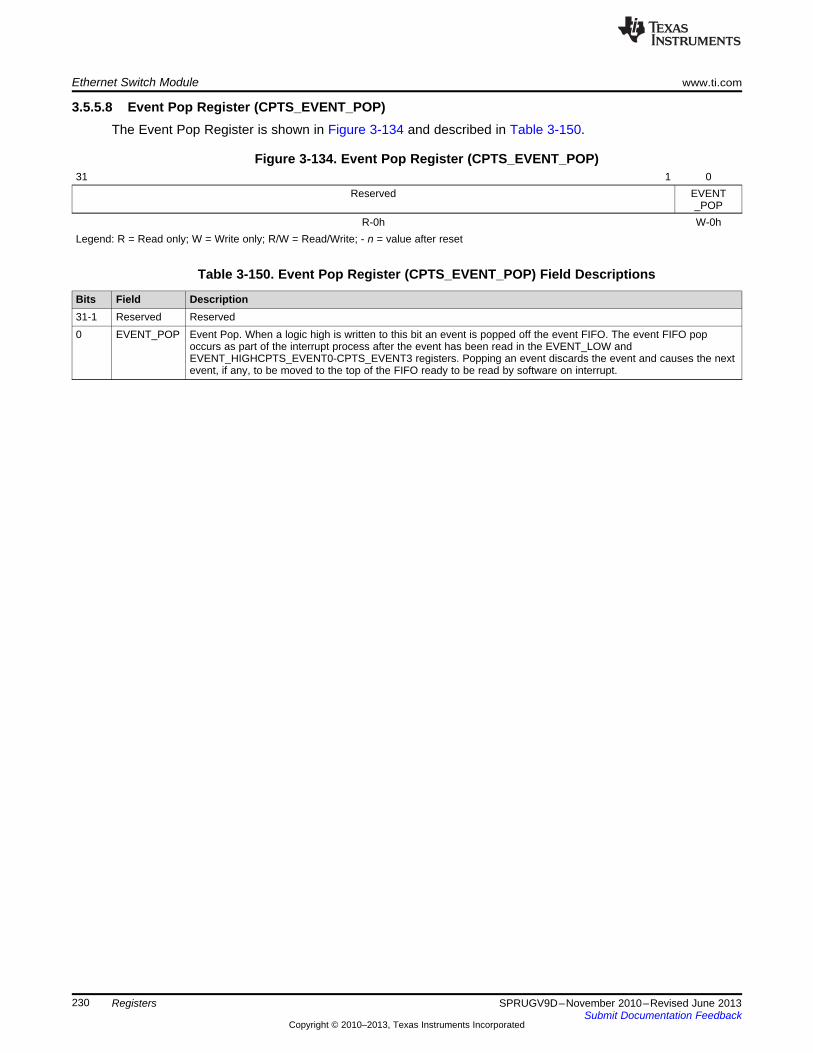
Ethernet Switch Module www.ti.com
230 SPRUGV9D–November 2010–Revised June 2013Submit Documentation Feedback
Copyright © 2010–2013, Texas Instruments Incorporated
Registers
3.5.5.8 Event Pop Register (CPTS_EVENT_POP)The Event Pop Register is shown in Figure 3-134 and described in Table 3-150.
Figure 3-134. Event Pop Register (CPTS_EVENT_POP)31 1 0
Reserved EVENT_POP
R-0h W-0hLegend: R = Read only; W = Write only; R/W = Read/Write; - n = value after reset
Table 3-150. Event Pop Register (CPTS_EVENT_POP) Field Descriptions
Bits Field Description31-1 Reserved Reserved0 EVENT_POP Event Pop. When a logic high is written to this bit an event is popped off the event FIFO. The event FIFO pop
occurs as part of the interrupt process after the event has been read in the EVENT_LOW andEVENT_HIGHCPTS_EVENT0-CPTS_EVENT3 registers. Popping an event discards the event and causes the nextevent, if any, to be moved to the top of the FIFO ready to be read by software on interrupt.
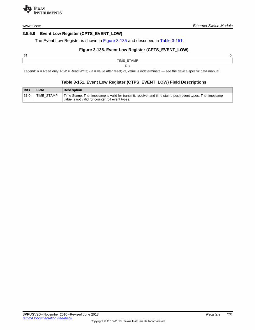
www.ti.com Ethernet Switch Module
231SPRUGV9D–November 2010–Revised June 2013Submit Documentation Feedback
Copyright © 2010–2013, Texas Instruments Incorporated
Registers
3.5.5.9 Event Low Register (CPTS_EVENT_LOW)The Event Low Register is shown in Figure 3-135 and described in Table 3-151.
Figure 3-135. Event Low Register (CPTS_EVENT_LOW)31 0
TIME_STAMPR-x
Legend: R = Read only; R/W = Read/Write; - n = value after reset; -x, value is indeterminate — see the device-specific data manual
Table 3-151. Event Low Register (CTPS_EVENT_LOW) Field Descriptions
Bits Field Description31-0 TIME_STAMP Time Stamp. The timestamp is valid for transmit, receive, and time stamp push event types. The timestamp
value is not valid for counter roll event types.
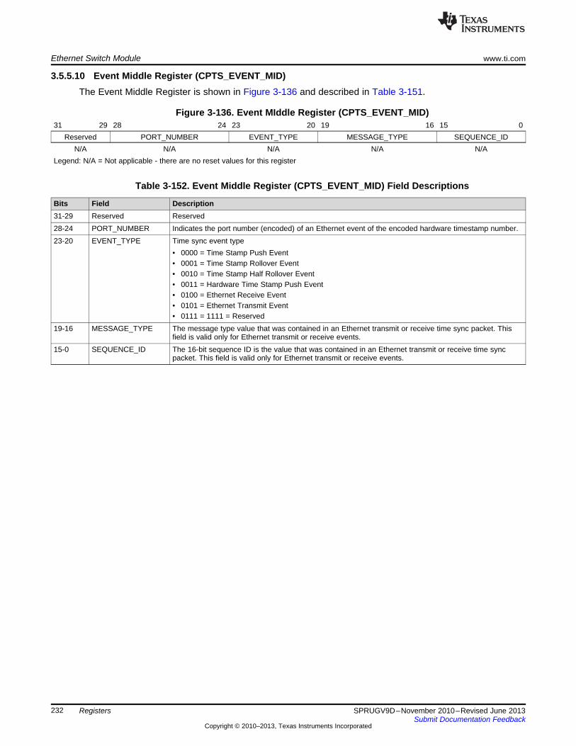
Ethernet Switch Module www.ti.com
232 SPRUGV9D–November 2010–Revised June 2013Submit Documentation Feedback
Copyright © 2010–2013, Texas Instruments Incorporated
Registers
3.5.5.10 Event Middle Register (CPTS_EVENT_MID)The Event Middle Register is shown in Figure 3-136 and described in Table 3-151.
Figure 3-136. Event MIddle Register (CPTS_EVENT_MID)31 29 28 24 23 20 19 16 15 0
Reserved PORT_NUMBER EVENT_TYPE MESSAGE_TYPE SEQUENCE_IDN/A N/A N/A N/A N/A
Legend: N/A = Not applicable - there are no reset values for this register
Table 3-152. Event Middle Register (CPTS_EVENT_MID) Field Descriptions
Bits Field Description31-29 Reserved Reserved28-24 PORT_NUMBER Indicates the port number (encoded) of an Ethernet event of the encoded hardware timestamp number.23-20 EVENT_TYPE Time sync event type
• 0000 = Time Stamp Push Event• 0001 = Time Stamp Rollover Event• 0010 = Time Stamp Half Rollover Event• 0011 = Hardware Time Stamp Push Event• 0100 = Ethernet Receive Event• 0101 = Ethernet Transmit Event• 0111 = 1111 = Reserved
19-16 MESSAGE_TYPE The message type value that was contained in an Ethernet transmit or receive time sync packet. Thisfield is valid only for Ethernet transmit or receive events.
15-0 SEQUENCE_ID The 16-bit sequence ID is the value that was contained in an Ethernet transmit or receive time syncpacket. This field is valid only for Ethernet transmit or receive events.
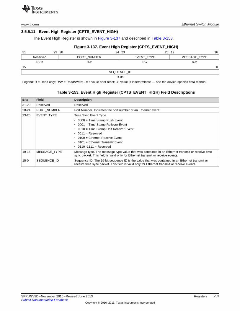
www.ti.com Ethernet Switch Module
233SPRUGV9D–November 2010–Revised June 2013Submit Documentation Feedback
Copyright © 2010–2013, Texas Instruments Incorporated
Registers
3.5.5.11 Event High Register (CPTS_EVENT_HIGH)The Event High Register is shown in Figure 3-137 and described in Table 3-153.
Figure 3-137. Event High Register (CPTS_EVENT_HIGH)31 29 28 24 23 20 19 16
Reserved PORT_NUMBER EVENT_TYPE MESSAGE_TYPER-0h R-x R-x R-x
15 0SEQUENCE_ID
R-0hLegend: R = Read only; R/W = Read/Write; - n = value after reset; -x, value is indeterminate — see the device-specific data manual
Table 3-153. Event High Register (CPTS_EVENT_HIGH) Field Descriptions
Bits Field Description31-29 Reserved Reserved28-24 PORT_NUMBER Port Number. Indicates the port number of an Ethernet event.23-20 EVENT_TYPE Time Sync Event Type.
• 0000 = Time Stamp Push Event• 0001 = Time Stamp Rollover Event• 0010 = Time Stamp Half Rollover Event• 0011 = Reserved• 0100 = Ethernet Receive Event• 0101 = Ethernet Transmit Event• 0110 -1111 = Reserved
19-16 MESSAGE_TYPE Message type. The message type value that was contained in an Ethernet transmit or receive timesync packet. This field is valid only for Ethernet transmit or receive events.
15-0 SEQUENCE_ID Sequence ID. The 16-bit sequence ID is the value that was contained in an Ethernet transmit orreceive time sync packet. This field is valid only for Ethernet transmit or receive events.
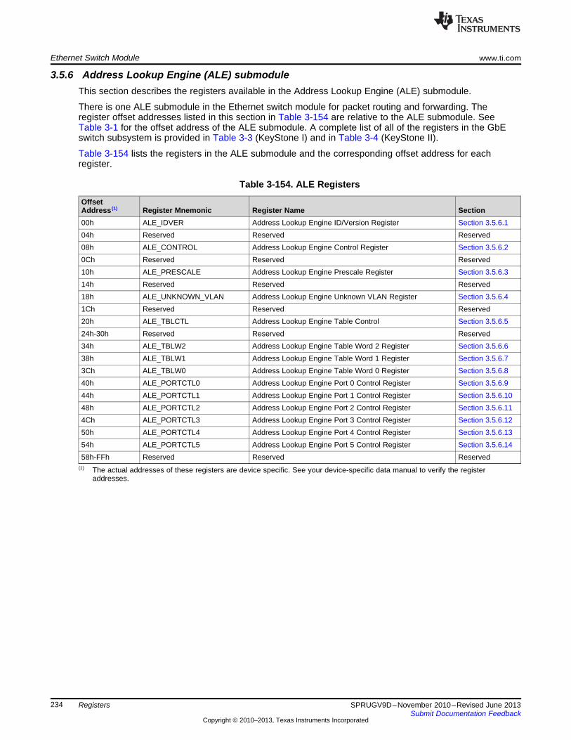
Ethernet Switch Module www.ti.com
234 SPRUGV9D–November 2010–Revised June 2013Submit Documentation Feedback
Copyright © 2010–2013, Texas Instruments Incorporated
Registers
3.5.6 Address Lookup Engine (ALE) submoduleThis section describes the registers available in the Address Lookup Engine (ALE) submodule.
There is one ALE submodule in the Ethernet switch module for packet routing and forwarding. Theregister offset addresses listed in this section in Table 3-154 are relative to the ALE submodule. SeeTable 3-1 for the offset address of the ALE submodule. A complete list of all of the registers in the GbEswitch subsystem is provided in Table 3-3 (KeyStone I) and in Table 3-4 (KeyStone II).
Table 3-154 lists the registers in the ALE submodule and the corresponding offset address for eachregister.
(1) The actual addresses of these registers are device specific. See your device-specific data manual to verify the registeraddresses.
Table 3-154. ALE Registers
OffsetAddress (1) Register Mnemonic Register Name Section00h ALE_IDVER Address Lookup Engine ID/Version Register Section 3.5.6.104h Reserved Reserved Reserved08h ALE_CONTROL Address Lookup Engine Control Register Section 3.5.6.20Ch Reserved Reserved Reserved10h ALE_PRESCALE Address Lookup Engine Prescale Register Section 3.5.6.314h Reserved Reserved Reserved18h ALE_UNKNOWN_VLAN Address Lookup Engine Unknown VLAN Register Section 3.5.6.41Ch Reserved Reserved Reserved20h ALE_TBLCTL Address Lookup Engine Table Control Section 3.5.6.524h-30h Reserved Reserved Reserved34h ALE_TBLW2 Address Lookup Engine Table Word 2 Register Section 3.5.6.638h ALE_TBLW1 Address Lookup Engine Table Word 1 Register Section 3.5.6.73Ch ALE_TBLW0 Address Lookup Engine Table Word 0 Register Section 3.5.6.840h ALE_PORTCTL0 Address Lookup Engine Port 0 Control Register Section 3.5.6.944h ALE_PORTCTL1 Address Lookup Engine Port 1 Control Register Section 3.5.6.1048h ALE_PORTCTL2 Address Lookup Engine Port 2 Control Register Section 3.5.6.114Ch ALE_PORTCTL3 Address Lookup Engine Port 3 Control Register Section 3.5.6.1250h ALE_PORTCTL4 Address Lookup Engine Port 4 Control Register Section 3.5.6.1354h ALE_PORTCTL5 Address Lookup Engine Port 5 Control Register Section 3.5.6.1458h-FFh Reserved Reserved Reserved
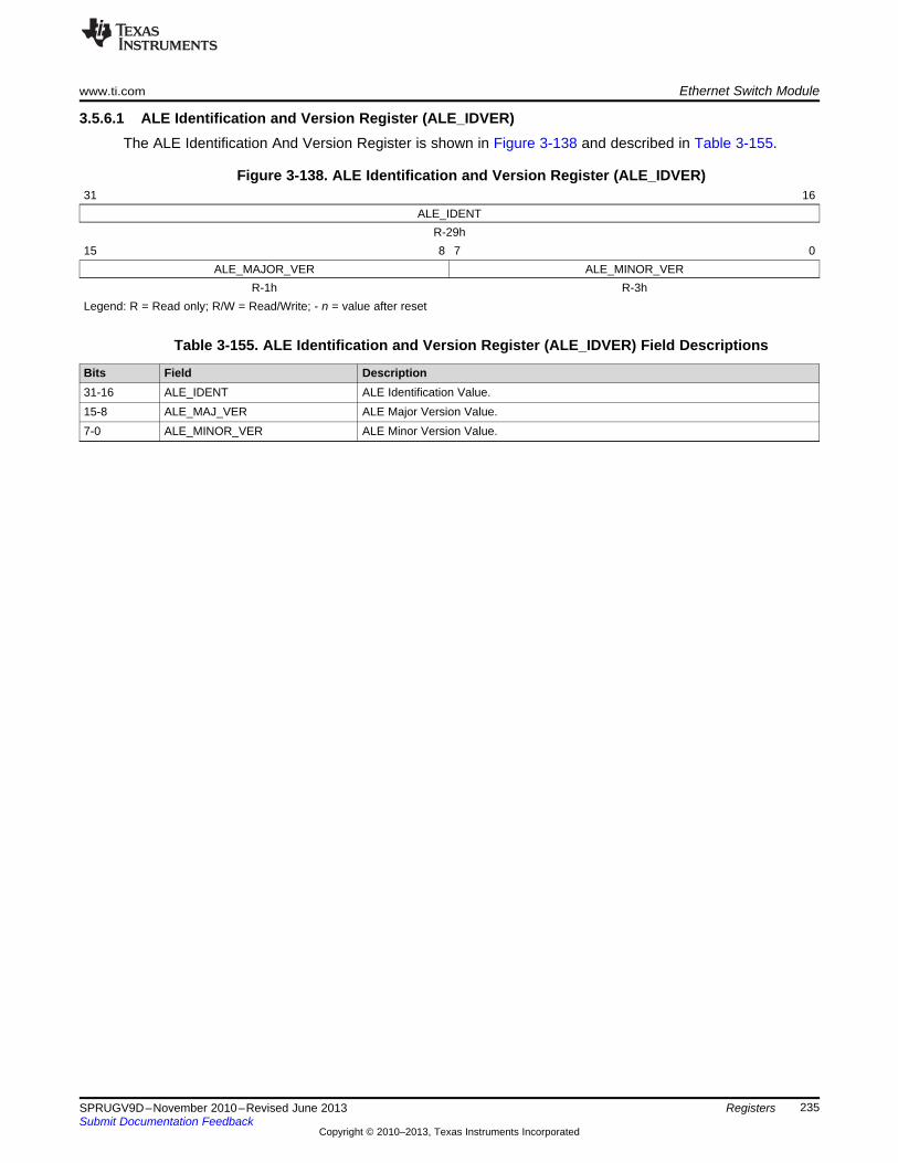
www.ti.com Ethernet Switch Module
235SPRUGV9D–November 2010–Revised June 2013Submit Documentation Feedback
Copyright © 2010–2013, Texas Instruments Incorporated
Registers
3.5.6.1 ALE Identification and Version Register (ALE_IDVER)The ALE Identification And Version Register is shown in Figure 3-138 and described in Table 3-155.
Figure 3-138. ALE Identification and Version Register (ALE_IDVER)31 16
ALE_IDENTR-29h
15 8 7 0ALE_MAJOR_VER ALE_MINOR_VER
R-1h R-3hLegend: R = Read only; R/W = Read/Write; - n = value after reset
Table 3-155. ALE Identification and Version Register (ALE_IDVER) Field Descriptions
Bits Field Description31-16 ALE_IDENT ALE Identification Value.15-8 ALE_MAJ_VER ALE Major Version Value.7-0 ALE_MINOR_VER ALE Minor Version Value.
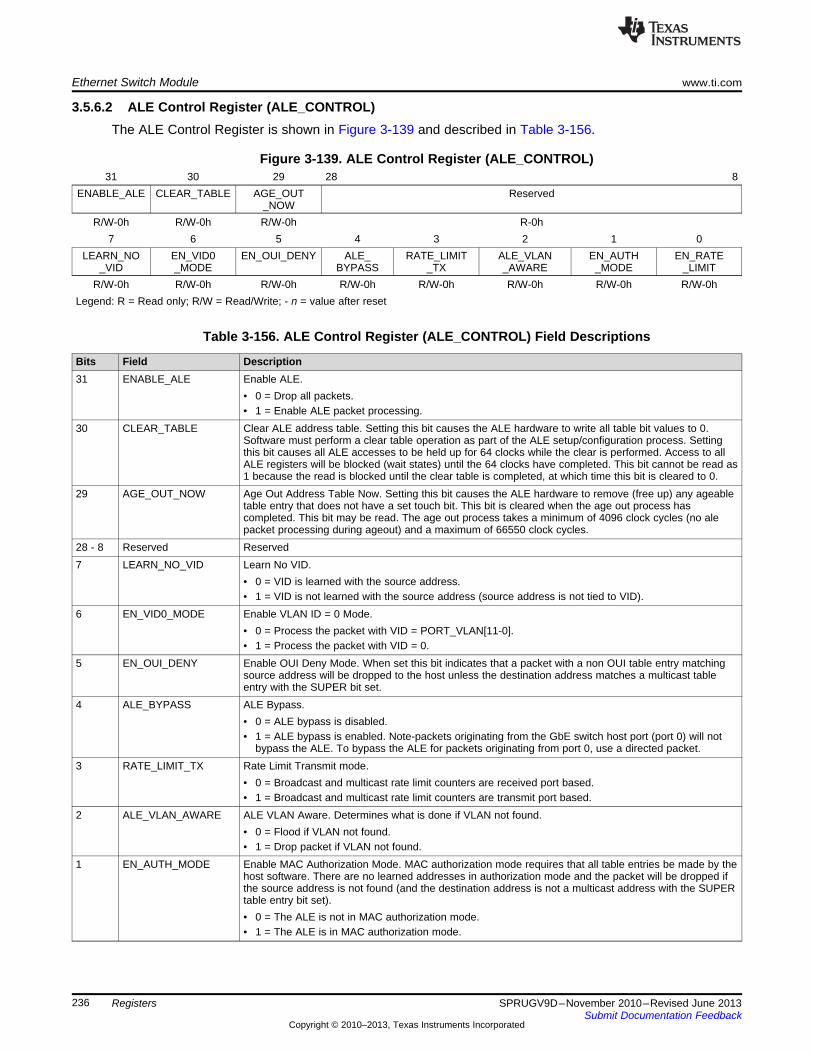
Ethernet Switch Module www.ti.com
236 SPRUGV9D–November 2010–Revised June 2013Submit Documentation Feedback
Copyright © 2010–2013, Texas Instruments Incorporated
Registers
3.5.6.2 ALE Control Register (ALE_CONTROL)The ALE Control Register is shown in Figure 3-139 and described in Table 3-156.
Figure 3-139. ALE Control Register (ALE_CONTROL)31 30 29 28 8
ENABLE_ALE CLEAR_TABLE AGE_OUT_NOW
Reserved
R/W-0h R/W-0h R/W-0h R-0h7 6 5 4 3 2 1 0
LEARN_NO_VID
EN_VID0_MODE
EN_OUI_DENY ALE_BYPASS
RATE_LIMIT_TX
ALE_VLAN_AWARE
EN_AUTH_MODE
EN_RATE_LIMIT
R/W-0h R/W-0h R/W-0h R/W-0h R/W-0h R/W-0h R/W-0h R/W-0hLegend: R = Read only; R/W = Read/Write; - n = value after reset
Table 3-156. ALE Control Register (ALE_CONTROL) Field Descriptions
Bits Field Description31 ENABLE_ALE Enable ALE.
• 0 = Drop all packets.• 1 = Enable ALE packet processing.
30 CLEAR_TABLE Clear ALE address table. Setting this bit causes the ALE hardware to write all table bit values to 0.Software must perform a clear table operation as part of the ALE setup/configuration process. Settingthis bit causes all ALE accesses to be held up for 64 clocks while the clear is performed. Access to allALE registers will be blocked (wait states) until the 64 clocks have completed. This bit cannot be read as1 because the read is blocked until the clear table is completed, at which time this bit is cleared to 0.
29 AGE_OUT_NOW Age Out Address Table Now. Setting this bit causes the ALE hardware to remove (free up) any ageabletable entry that does not have a set touch bit. This bit is cleared when the age out process hascompleted. This bit may be read. The age out process takes a minimum of 4096 clock cycles (no alepacket processing during ageout) and a maximum of 66550 clock cycles.
28 - 8 Reserved Reserved7 LEARN_NO_VID Learn No VID.
• 0 = VID is learned with the source address.• 1 = VID is not learned with the source address (source address is not tied to VID).
6 EN_VID0_MODE Enable VLAN ID = 0 Mode.• 0 = Process the packet with VID = PORT_VLAN[11-0].• 1 = Process the packet with VID = 0.
5 EN_OUI_DENY Enable OUI Deny Mode. When set this bit indicates that a packet with a non OUI table entry matchingsource address will be dropped to the host unless the destination address matches a multicast tableentry with the SUPER bit set.
4 ALE_BYPASS ALE Bypass.• 0 = ALE bypass is disabled.• 1 = ALE bypass is enabled. Note-packets originating from the GbE switch host port (port 0) will not
bypass the ALE. To bypass the ALE for packets originating from port 0, use a directed packet.3 RATE_LIMIT_TX Rate Limit Transmit mode.
• 0 = Broadcast and multicast rate limit counters are received port based.• 1 = Broadcast and multicast rate limit counters are transmit port based.
2 ALE_VLAN_AWARE ALE VLAN Aware. Determines what is done if VLAN not found.• 0 = Flood if VLAN not found.• 1 = Drop packet if VLAN not found.
1 EN_AUTH_MODE Enable MAC Authorization Mode. MAC authorization mode requires that all table entries be made by thehost software. There are no learned addresses in authorization mode and the packet will be dropped ifthe source address is not found (and the destination address is not a multicast address with the SUPERtable entry bit set).• 0 = The ALE is not in MAC authorization mode.• 1 = The ALE is in MAC authorization mode.
www.ti.com Ethernet Switch Module
237SPRUGV9D–November 2010–Revised June 2013Submit Documentation Feedback
Copyright © 2010–2013, Texas Instruments Incorporated
Registers
Table 3-156. ALE Control Register (ALE_CONTROL) Field Descriptions (continued)Bits Field Description0 EN_RATE_LIMIT Enable Broadcast and Multicast Rate Limit.
• 0 = Broadcast/Multicast rates not limited.• 1 = Broadcast/Multicast packet reception limited to the port control register rate limit fields.
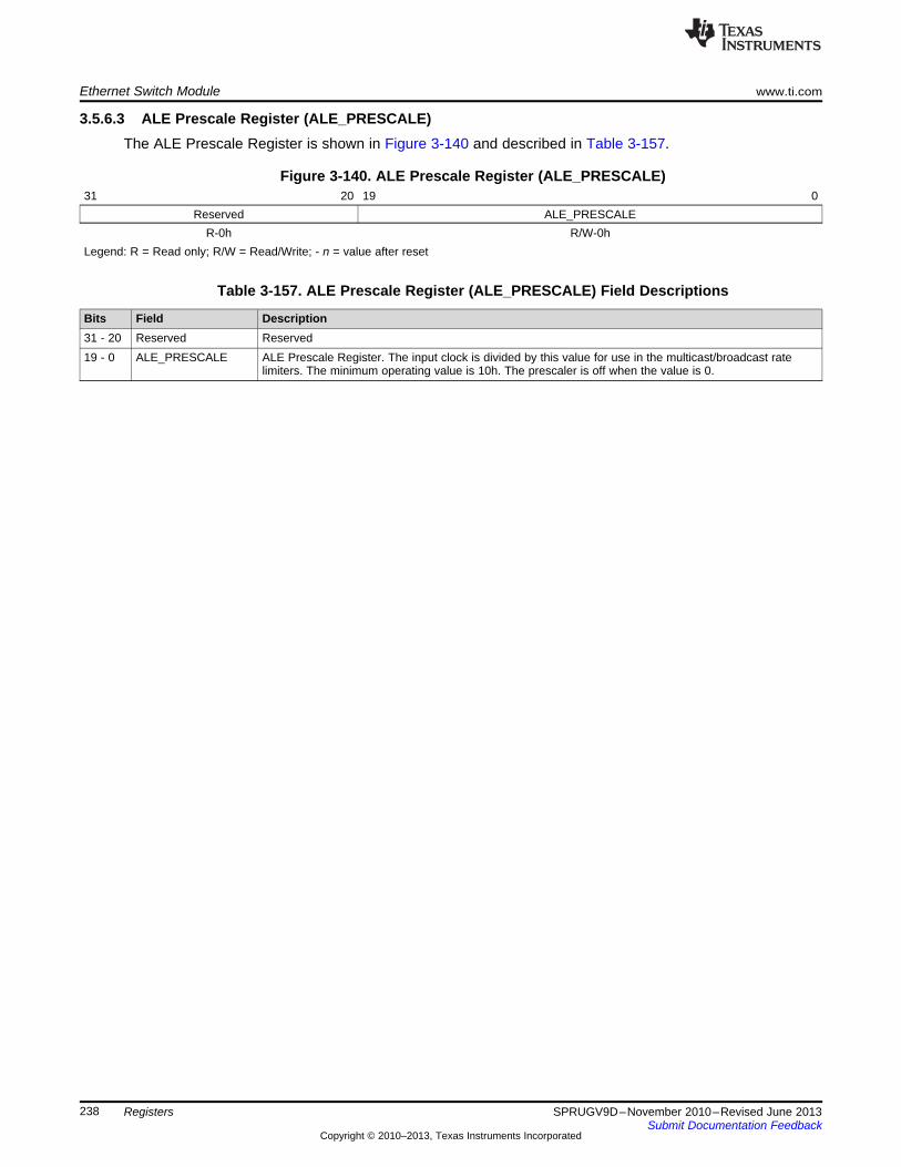
Ethernet Switch Module www.ti.com
238 SPRUGV9D–November 2010–Revised June 2013Submit Documentation Feedback
Copyright © 2010–2013, Texas Instruments Incorporated
Registers
3.5.6.3 ALE Prescale Register (ALE_PRESCALE)The ALE Prescale Register is shown in Figure 3-140 and described in Table 3-157.
Figure 3-140. ALE Prescale Register (ALE_PRESCALE)31 20 19 0
Reserved ALE_PRESCALER-0h R/W-0h
Legend: R = Read only; R/W = Read/Write; - n = value after reset
Table 3-157. ALE Prescale Register (ALE_PRESCALE) Field Descriptions
Bits Field Description31 - 20 Reserved Reserved19 - 0 ALE_PRESCALE ALE Prescale Register. The input clock is divided by this value for use in the multicast/broadcast rate
limiters. The minimum operating value is 10h. The prescaler is off when the value is 0.
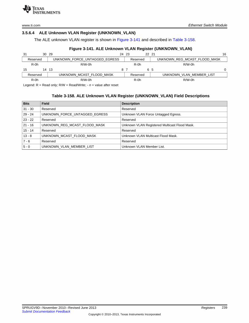
www.ti.com Ethernet Switch Module
239SPRUGV9D–November 2010–Revised June 2013Submit Documentation Feedback
Copyright © 2010–2013, Texas Instruments Incorporated
Registers
3.5.6.4 ALE Unknown VLAN Register (UNKNOWN_VLAN)The ALE unknown VLAN register is shown in Figure 3-141 and described in Table 3-158.
Figure 3-141. ALE Unknown VLAN Register (UNKNOWN_VLAN)31 30 29 24 23 22 21 16
Reserved UNKNOWN_FORCE_UNTAGGED_EGRESS Reserved UNKNOWN_REG_MCAST_FLOOD_MASKR-0h R/W-0h R-0h R/W-0h
15 14 13 8 7 6 5 0Reserved UNKNOWN_MCAST_FLOOD_MASK Reserved UNKNOWN_VLAN_MEMBER_LIST
R-0h R/W-0h R-0h R/W-0hLegend: R = Read only; R/W = Read/Write; - n = value after reset
Table 3-158. ALE Unknown VLAN Register (UNKNOWN_VLAN) Field Descriptions
Bits Field Description31 - 30 Reserved Reserved29 - 24 UNKNOWN_FORCE_UNTAGGED_EGRESS Unknown VLAN Force Untagged Egress.23 - 22 Reserved Reserved21 - 16 UNKNOWN_REG_MCAST_FLOOD_MASK Unknown VLAN Registered Multicast Flood Mask.15 - 14 Reserved Reserved13 - 8 UNKNOWN_MCAST_FLOOD_MASK Unknown VLAN Multicast Flood Mask.7 - 6 Reserved Reserved5 - 0 UNKNOWN_VLAN_MEMBER_LIST Unknown VLAN Member List.
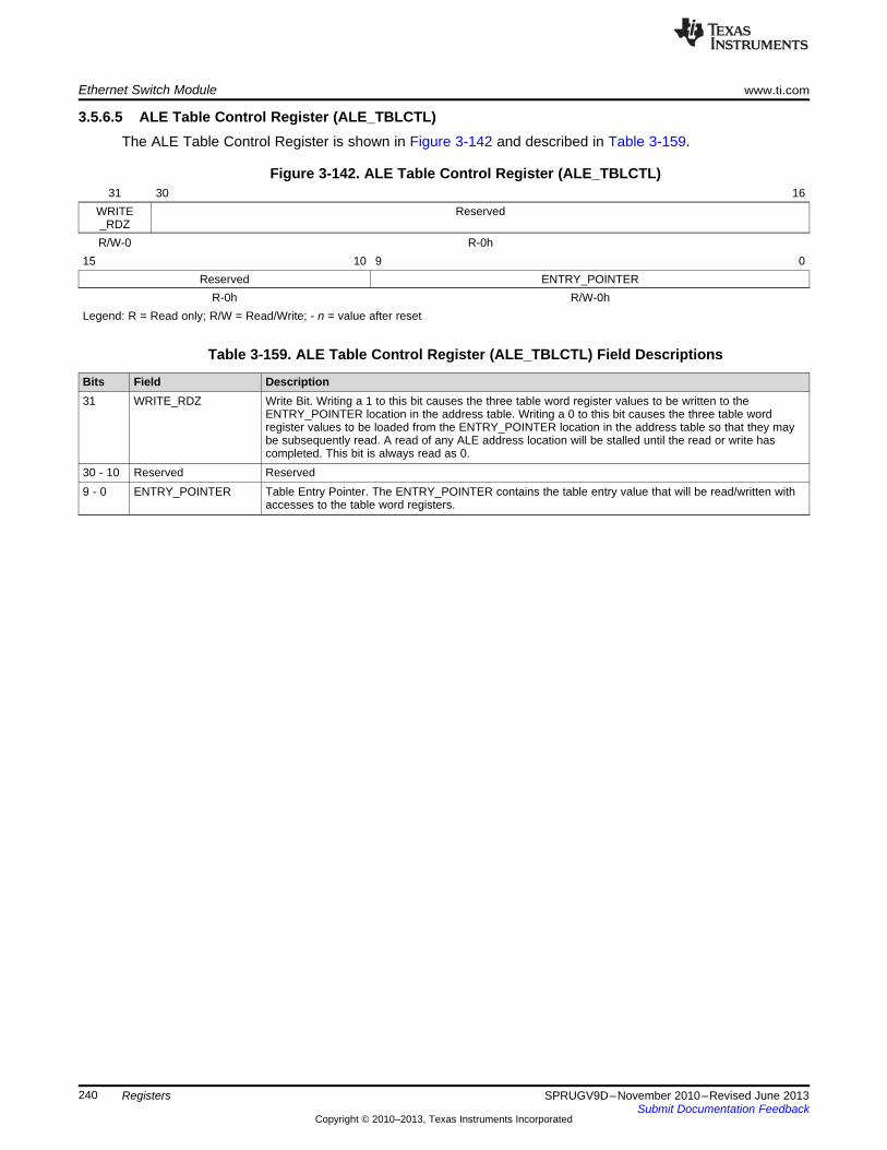
Ethernet Switch Module www.ti.com
240 SPRUGV9D–November 2010–Revised June 2013Submit Documentation Feedback
Copyright © 2010–2013, Texas Instruments Incorporated
Registers
3.5.6.5 ALE Table Control Register (ALE_TBLCTL)The ALE Table Control Register is shown in Figure 3-142 and described in Table 3-159.
Figure 3-142. ALE Table Control Register (ALE_TBLCTL)31 30 16
WRITE_RDZ
Reserved
R/W-0 R-0h15 10 9 0
Reserved ENTRY_POINTERR-0h R/W-0h
Legend: R = Read only; R/W = Read/Write; - n = value after reset
Table 3-159. ALE Table Control Register (ALE_TBLCTL) Field Descriptions
Bits Field Description31 WRITE_RDZ Write Bit. Writing a 1 to this bit causes the three table word register values to be written to the
ENTRY_POINTER location in the address table. Writing a 0 to this bit causes the three table wordregister values to be loaded from the ENTRY_POINTER location in the address table so that they maybe subsequently read. A read of any ALE address location will be stalled until the read or write hascompleted. This bit is always read as 0.
30 - 10 Reserved Reserved9 - 0 ENTRY_POINTER Table Entry Pointer. The ENTRY_POINTER contains the table entry value that will be read/written with
accesses to the table word registers.
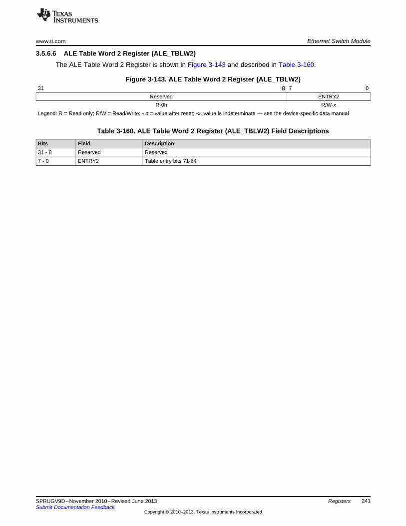
www.ti.com Ethernet Switch Module
241SPRUGV9D–November 2010–Revised June 2013Submit Documentation Feedback
Copyright © 2010–2013, Texas Instruments Incorporated
Registers
3.5.6.6 ALE Table Word 2 Register (ALE_TBLW2)The ALE Table Word 2 Register is shown in Figure 3-143 and described in Table 3-160.
Figure 3-143. ALE Table Word 2 Register (ALE_TBLW2)31 8 7 0
Reserved ENTRY2R-0h R/W-x
Legend: R = Read only; R/W = Read/Write; - n = value after reset; -x, value is indeterminate — see the device-specific data manual
Table 3-160. ALE Table Word 2 Register (ALE_TBLW2) Field Descriptions
Bits Field Description31 - 8 Reserved Reserved7 - 0 ENTRY2 Table entry bits 71-64
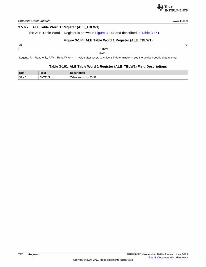
Ethernet Switch Module www.ti.com
242 SPRUGV9D–November 2010–Revised June 2013Submit Documentation Feedback
Copyright © 2010–2013, Texas Instruments Incorporated
Registers
3.5.6.7 ALE Table Word 1 Register (ALE_TBLW1)The ALE Table Word 1 Register is shown in Figure 3-144 and described in Table 3-161.
Figure 3-144. ALE Table Word 1 Register (ALE_TBLW1)31 0
ENTRY1R/W-x
Legend: R = Read only; R/W = Read/Write; - n = value after reset; -x, value is indeterminate — see the device-specific data manual
Table 3-161. ALE Table Word 1 Register (ALE_TBLW2) Field Descriptions
Bits Field Description31 - 0 ENTRY1 Table entry bits 63-32
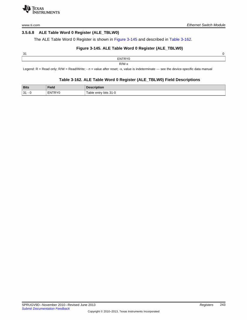
www.ti.com Ethernet Switch Module
243SPRUGV9D–November 2010–Revised June 2013Submit Documentation Feedback
Copyright © 2010–2013, Texas Instruments Incorporated
Registers
3.5.6.8 ALE Table Word 0 Register (ALE_TBLW0)The ALE Table Word 0 Register is shown in Figure 3-145 and described in Table 3-162.
Figure 3-145. ALE Table Word 0 Register (ALE_TBLW0)31 0
ENTRY0R/W-x
Legend: R = Read only; R/W = Read/Write; - n = value after reset; -x, value is indeterminate — see the device-specific data manual
Table 3-162. ALE Table Word 0 Register (ALE_TBLW0) Field Descriptions
Bits Field Description31 - 0 ENTRY0 Table entry bits 31-0
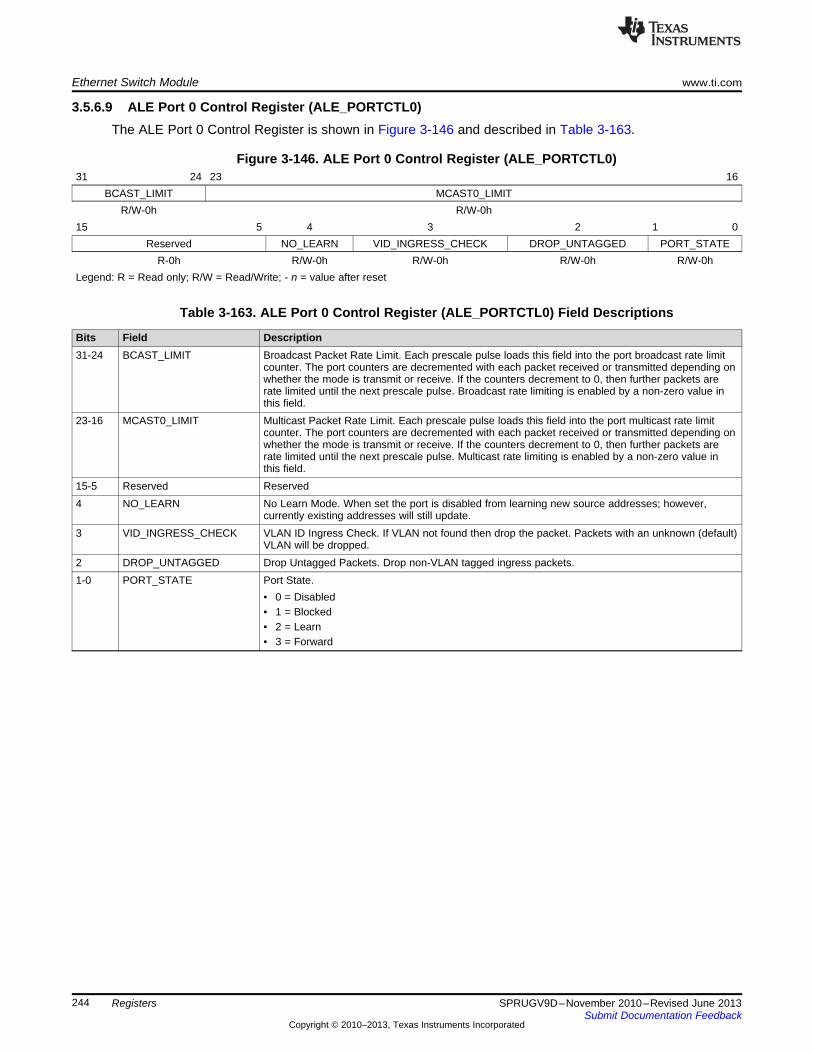
Ethernet Switch Module www.ti.com
244 SPRUGV9D–November 2010–Revised June 2013Submit Documentation Feedback
Copyright © 2010–2013, Texas Instruments Incorporated
Registers
3.5.6.9 ALE Port 0 Control Register (ALE_PORTCTL0)The ALE Port 0 Control Register is shown in Figure 3-146 and described in Table 3-163.
Figure 3-146. ALE Port 0 Control Register (ALE_PORTCTL0)31 24 23 16
BCAST_LIMIT MCAST0_LIMITR/W-0h R/W-0h
15 5 4 3 2 1 0Reserved NO_LEARN VID_INGRESS_CHECK DROP_UNTAGGED PORT_STATE
R-0h R/W-0h R/W-0h R/W-0h R/W-0hLegend: R = Read only; R/W = Read/Write; - n = value after reset
Table 3-163. ALE Port 0 Control Register (ALE_PORTCTL0) Field Descriptions
Bits Field Description31-24 BCAST_LIMIT Broadcast Packet Rate Limit. Each prescale pulse loads this field into the port broadcast rate limit
counter. The port counters are decremented with each packet received or transmitted depending onwhether the mode is transmit or receive. If the counters decrement to 0, then further packets arerate limited until the next prescale pulse. Broadcast rate limiting is enabled by a non-zero value inthis field.
23-16 MCAST0_LIMIT Multicast Packet Rate Limit. Each prescale pulse loads this field into the port multicast rate limitcounter. The port counters are decremented with each packet received or transmitted depending onwhether the mode is transmit or receive. If the counters decrement to 0, then further packets arerate limited until the next prescale pulse. Multicast rate limiting is enabled by a non-zero value inthis field.
15-5 Reserved Reserved4 NO_LEARN No Learn Mode. When set the port is disabled from learning new source addresses; however,
currently existing addresses will still update.3 VID_INGRESS_CHECK VLAN ID Ingress Check. If VLAN not found then drop the packet. Packets with an unknown (default)
VLAN will be dropped.2 DROP_UNTAGGED Drop Untagged Packets. Drop non-VLAN tagged ingress packets.1-0 PORT_STATE Port State.
• 0 = Disabled• 1 = Blocked• 2 = Learn• 3 = Forward
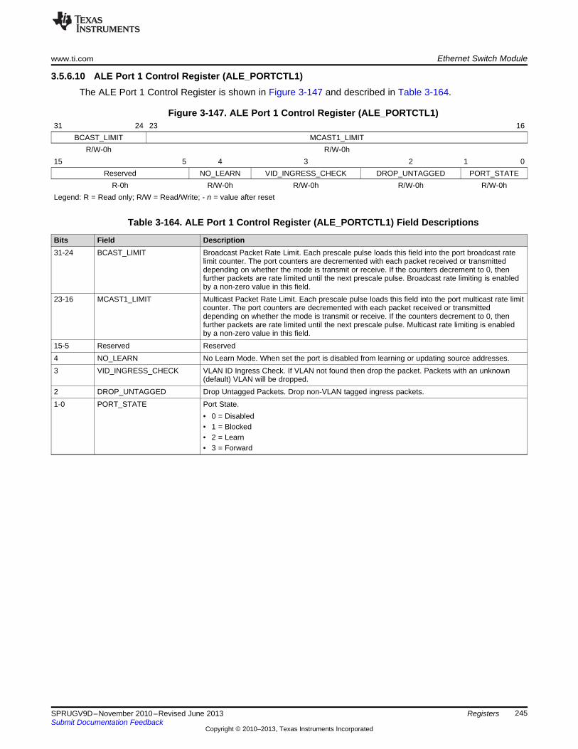
www.ti.com Ethernet Switch Module
245SPRUGV9D–November 2010–Revised June 2013Submit Documentation Feedback
Copyright © 2010–2013, Texas Instruments Incorporated
Registers
3.5.6.10 ALE Port 1 Control Register (ALE_PORTCTL1)The ALE Port 1 Control Register is shown in Figure 3-147 and described in Table 3-164.
Figure 3-147. ALE Port 1 Control Register (ALE_PORTCTL1)31 24 23 16
BCAST_LIMIT MCAST1_LIMITR/W-0h R/W-0h
15 5 4 3 2 1 0Reserved NO_LEARN VID_INGRESS_CHECK DROP_UNTAGGED PORT_STATE
R-0h R/W-0h R/W-0h R/W-0h R/W-0hLegend: R = Read only; R/W = Read/Write; - n = value after reset
Table 3-164. ALE Port 1 Control Register (ALE_PORTCTL1) Field Descriptions
Bits Field Description31-24 BCAST_LIMIT Broadcast Packet Rate Limit. Each prescale pulse loads this field into the port broadcast rate
limit counter. The port counters are decremented with each packet received or transmitteddepending on whether the mode is transmit or receive. If the counters decrement to 0, thenfurther packets are rate limited until the next prescale pulse. Broadcast rate limiting is enabledby a non-zero value in this field.
23-16 MCAST1_LIMIT Multicast Packet Rate Limit. Each prescale pulse loads this field into the port multicast rate limitcounter. The port counters are decremented with each packet received or transmitteddepending on whether the mode is transmit or receive. If the counters decrement to 0, thenfurther packets are rate limited until the next prescale pulse. Multicast rate limiting is enabledby a non-zero value in this field.
15-5 Reserved Reserved4 NO_LEARN No Learn Mode. When set the port is disabled from learning or updating source addresses.3 VID_INGRESS_CHECK VLAN ID Ingress Check. If VLAN not found then drop the packet. Packets with an unknown
(default) VLAN will be dropped.2 DROP_UNTAGGED Drop Untagged Packets. Drop non-VLAN tagged ingress packets.1-0 PORT_STATE Port State.
• 0 = Disabled• 1 = Blocked• 2 = Learn• 3 = Forward
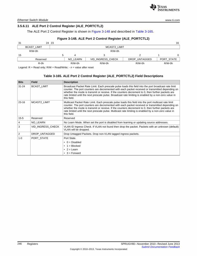
Ethernet Switch Module www.ti.com
246 SPRUGV9D–November 2010–Revised June 2013Submit Documentation Feedback
Copyright © 2010–2013, Texas Instruments Incorporated
Registers
3.5.6.11 ALE Port 2 Control Register (ALE_PORTCTL2)The ALE Port 2 Control Register is shown in Figure 3-148 and described in Table 3-165.
Figure 3-148. ALE Port 2 Control Register (ALE_PORTCTL2)31 24 23 16
BCAST_LIMIT MCAST2_LIMITR/W-0h R/W-0h
15 5 4 3 2 1 0Reserved NO_LEARN VID_INGRESS_CHECK DROP_UNTAGGED PORT_STATE
R-0h R/W-0h R/W-0h R/W-0h R/W-0hLegend: R = Read only; R/W = Read/Write; - n = value after reset
Table 3-165. ALE Port 2 Control Register (ALE_PORTCTL2) Field Descriptions
Bits Field Description31-24 BCAST_LIMIT Broadcast Packet Rate Limit. Each prescale pulse loads this field into the port broadcast rate limit
counter. The port counters are decremented with each packet received or transmitted depending onwhether the mode is transmit or receive. If the counters decrement to 0, then further packets arerate limited until the next prescale pulse. Broadcast rate limiting is enabled by a non-zero value inthis field.
23-16 MCAST2_LIMIT Multicast Packet Rate Limit. Each prescale pulse loads this field into the port multicast rate limitcounter. The port counters are decremented with each packet received or transmitted depending onwhether the mode is transmit or receive. If the counters decrement to 0, then further packets arerate limited until the next prescale pulse. Multicast rate limiting is enabled by a non-zero value inthis field.
15-5 Reserved Reserved4 NO_LEARN No Learn Mode. When set the port is disabled from learning or updating source addresses.3 VID_INGRESS_CHECK VLAN ID Ingress Check. If VLAN not found then drop the packet. Packets with an unknown (default)
VLAN will be dropped.2 DROP_UNTAGGED Drop Untagged Packets. Drop non-VLAN tagged ingress packets.1-0 PORT_STATE Port State.
• 0 = Disabled• 1 = Blocked• 2 = Learn• 3 = Forward
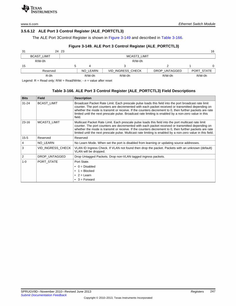
www.ti.com Ethernet Switch Module
247SPRUGV9D–November 2010–Revised June 2013Submit Documentation Feedback
Copyright © 2010–2013, Texas Instruments Incorporated
Registers
3.5.6.12 ALE Port 3 Control Register (ALE_PORTCTL3)The ALE Port 3Control Register is shown in Figure 3-149 and described in Table 3-166.
Figure 3-149. ALE Port 3 Control Register (ALE_PORTCTL3)31 24 23 16
BCAST_LIMIT MCAST3_LIMITR/W-0h R/W-0h
15 5 4 3 2 1 0Reserved NO_LEARN VID_INGRESS_CHECK DROP_UNTAGGED PORT_STATE
R-0h R/W-0h R/W-0h R/W-0h R/W-0hLegend: R = Read only; R/W = Read/Write; - n = value after reset
Table 3-166. ALE Port 3 Control Register (ALE_PORTCTL3) Field Descriptions
Bits Field Description31-24 BCAST_LIMIT Broadcast Packet Rate Limit. Each prescale pulse loads this field into the port broadcast rate limit
counter. The port counters are decremented with each packet received or transmitted depending onwhether the mode is transmit or receive. If the counters decrement to 0, then further packets are ratelimited until the next prescale pulse. Broadcast rate limiting is enabled by a non-zero value in thisfield.
23-16 MCAST3_LIMIT Multicast Packet Rate Limit. Each prescale pulse loads this field into the port multicast rate limitcounter. The port counters are decremented with each packet received or transmitted depending onwhether the mode is transmit or receive. If the counters decrement to 0, then further packets are ratelimited until the next prescale pulse. Multicast rate limiting is enabled by a non-zero value in this field.
15-5 Reserved Reserved4 NO_LEARN No Learn Mode. When set the port is disabled from learning or updating source addresses.3 VID_INGRESS_CHECK VLAN ID Ingress Check. If VLAN not found then drop the packet. Packets with an unknown (default)
VLAN will be dropped.2 DROP_UNTAGGED Drop Untagged Packets. Drop non-VLAN tagged ingress packets.1-0 PORT_STATE Port State.
• 0 = Disabled• 1 = Blocked• 2 = Learn• 3 = Forward
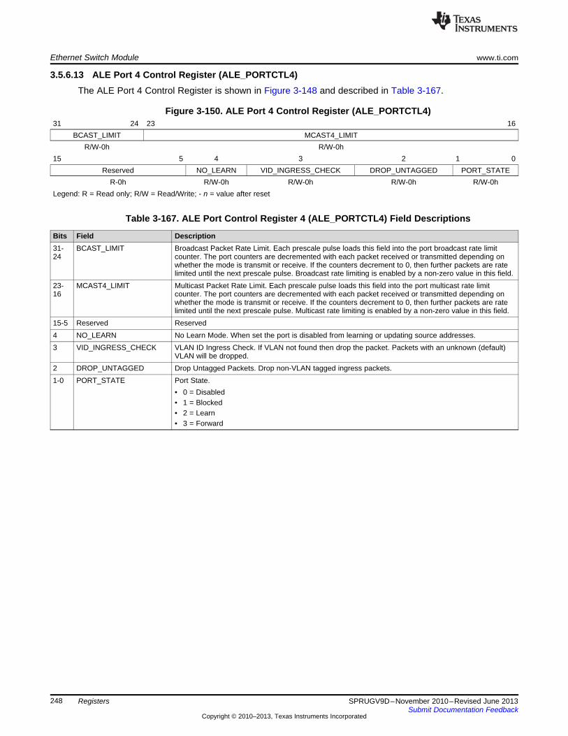
Ethernet Switch Module www.ti.com
248 SPRUGV9D–November 2010–Revised June 2013Submit Documentation Feedback
Copyright © 2010–2013, Texas Instruments Incorporated
Registers
3.5.6.13 ALE Port 4 Control Register (ALE_PORTCTL4)The ALE Port 4 Control Register is shown in Figure 3-148 and described in Table 3-167.
Figure 3-150. ALE Port 4 Control Register (ALE_PORTCTL4)31 24 23 16
BCAST_LIMIT MCAST4_LIMITR/W-0h R/W-0h
15 5 4 3 2 1 0Reserved NO_LEARN VID_INGRESS_CHECK DROP_UNTAGGED PORT_STATE
R-0h R/W-0h R/W-0h R/W-0h R/W-0hLegend: R = Read only; R/W = Read/Write; - n = value after reset
Table 3-167. ALE Port Control Register 4 (ALE_PORTCTL4) Field Descriptions
Bits Field Description31-24
BCAST_LIMIT Broadcast Packet Rate Limit. Each prescale pulse loads this field into the port broadcast rate limitcounter. The port counters are decremented with each packet received or transmitted depending onwhether the mode is transmit or receive. If the counters decrement to 0, then further packets are ratelimited until the next prescale pulse. Broadcast rate limiting is enabled by a non-zero value in this field.
23-16
MCAST4_LIMIT Multicast Packet Rate Limit. Each prescale pulse loads this field into the port multicast rate limitcounter. The port counters are decremented with each packet received or transmitted depending onwhether the mode is transmit or receive. If the counters decrement to 0, then further packets are ratelimited until the next prescale pulse. Multicast rate limiting is enabled by a non-zero value in this field.
15-5 Reserved Reserved4 NO_LEARN No Learn Mode. When set the port is disabled from learning or updating source addresses.3 VID_INGRESS_CHECK VLAN ID Ingress Check. If VLAN not found then drop the packet. Packets with an unknown (default)
VLAN will be dropped.2 DROP_UNTAGGED Drop Untagged Packets. Drop non-VLAN tagged ingress packets.1-0 PORT_STATE Port State.
• 0 = Disabled• 1 = Blocked• 2 = Learn• 3 = Forward
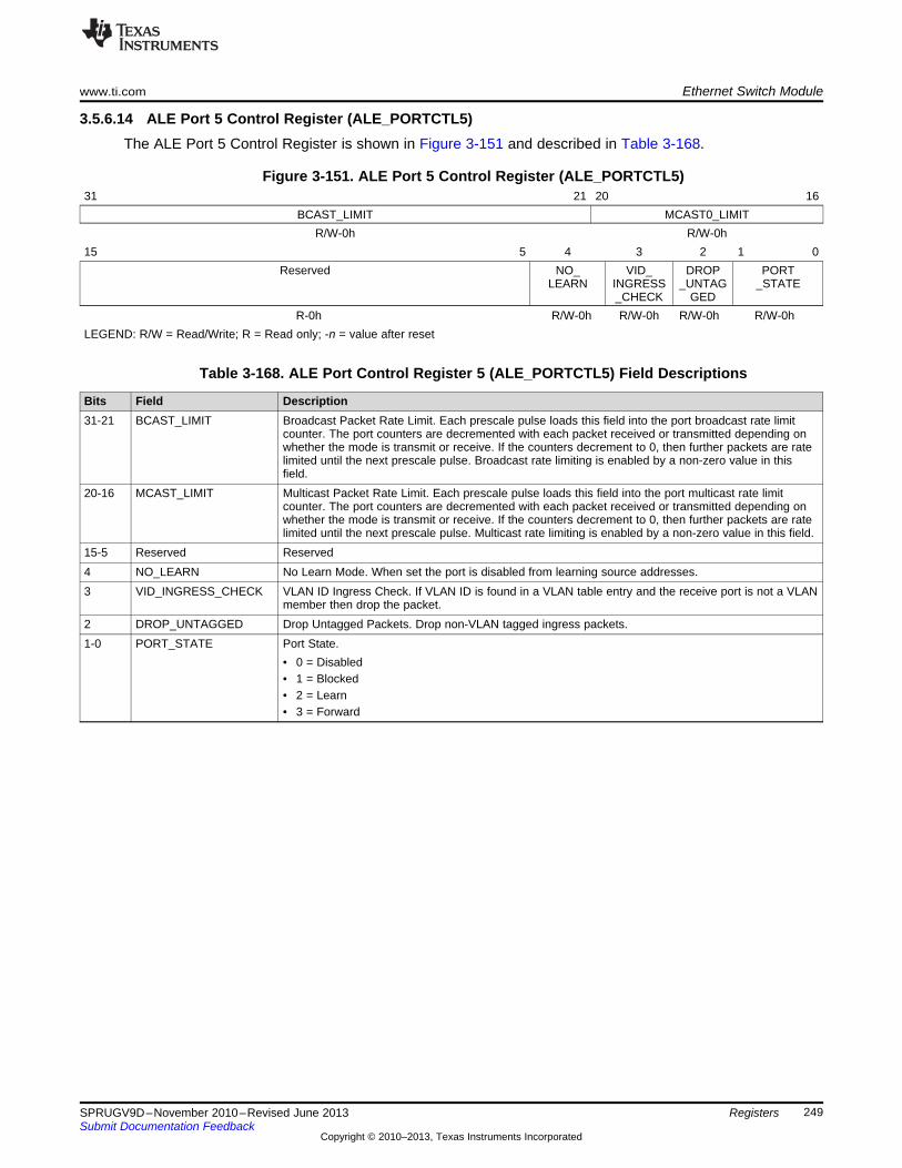
www.ti.com Ethernet Switch Module
249SPRUGV9D–November 2010–Revised June 2013Submit Documentation Feedback
Copyright © 2010–2013, Texas Instruments Incorporated
Registers
3.5.6.14 ALE Port 5 Control Register (ALE_PORTCTL5)The ALE Port 5 Control Register is shown in Figure 3-151 and described in Table 3-168.
Figure 3-151. ALE Port 5 Control Register (ALE_PORTCTL5)31 21 20 16
BCAST_LIMIT MCAST0_LIMITR/W-0h R/W-0h
15 5 4 3 2 1 0Reserved NO_
LEARNVID_
INGRESS_CHECK
DROP_UNTAG
GED
PORT_STATE
R-0h R/W-0h R/W-0h R/W-0h R/W-0hLEGEND: R/W = Read/Write; R = Read only; -n = value after reset
Table 3-168. ALE Port Control Register 5 (ALE_PORTCTL5) Field Descriptions
Bits Field Description31-21 BCAST_LIMIT Broadcast Packet Rate Limit. Each prescale pulse loads this field into the port broadcast rate limit
counter. The port counters are decremented with each packet received or transmitted depending onwhether the mode is transmit or receive. If the counters decrement to 0, then further packets are ratelimited until the next prescale pulse. Broadcast rate limiting is enabled by a non-zero value in thisfield.
20-16 MCAST_LIMIT Multicast Packet Rate Limit. Each prescale pulse loads this field into the port multicast rate limitcounter. The port counters are decremented with each packet received or transmitted depending onwhether the mode is transmit or receive. If the counters decrement to 0, then further packets are ratelimited until the next prescale pulse. Multicast rate limiting is enabled by a non-zero value in this field.
15-5 Reserved Reserved4 NO_LEARN No Learn Mode. When set the port is disabled from learning source addresses.3 VID_INGRESS_CHECK VLAN ID Ingress Check. If VLAN ID is found in a VLAN table entry and the receive port is not a VLAN
member then drop the packet.2 DROP_UNTAGGED Drop Untagged Packets. Drop non-VLAN tagged ingress packets.1-0 PORT_STATE Port State.
• 0 = Disabled• 1 = Blocked• 2 = Learn• 3 = Forward
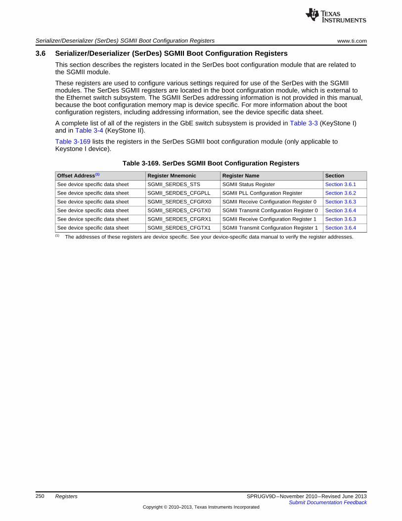
Serializer/Deserializer (SerDes) SGMII Boot Configuration Registers www.ti.com
250 SPRUGV9D–November 2010–Revised June 2013Submit Documentation Feedback
Copyright © 2010–2013, Texas Instruments Incorporated
Registers
3.6 Serializer/Deserializer (SerDes) SGMII Boot Configuration RegistersThis section describes the registers located in the SerDes boot configuration module that are related tothe SGMII module.
These registers are used to configure various settings required for use of the SerDes with the SGMIImodules. The SerDes SGMII registers are located in the boot configuration module, which is external tothe Ethernet switch subsystem. The SGMII SerDes addressing information is not provided in this manual,because the boot configuration memory map is device specific. For more information about the bootconfiguration registers, including addressing information, see the device specific data sheet.
A complete list of all of the registers in the GbE switch subsystem is provided in Table 3-3 (KeyStone I)and in Table 3-4 (KeyStone II).
Table 3-169 lists the registers in the SerDes SGMII boot configuration module (only applicable toKeystone I device).
(1) The addresses of these registers are device specific. See your device-specific data manual to verify the register addresses.
Table 3-169. SerDes SGMII Boot Configuration Registers
Offset Address (1) Register Mnemonic Register Name SectionSee device specific data sheet SGMII_SERDES_STS SGMII Status Register Section 3.6.1See device specific data sheet SGMII_SERDES_CFGPLL SGMII PLL Configuration Register Section 3.6.2See device specific data sheet SGMII_SERDES_CFGRX0 SGMII Receive Configuration Register 0 Section 3.6.3See device specific data sheet SGMII_SERDES_CFGTX0 SGMII Transmit Configuration Register 0 Section 3.6.4See device specific data sheet SGMII_SERDES_CFGRX1 SGMII Receive Configuration Register 1 Section 3.6.3See device specific data sheet SGMII_SERDES_CFGTX1 SGMII Transmit Configuration Register 1 Section 3.6.4
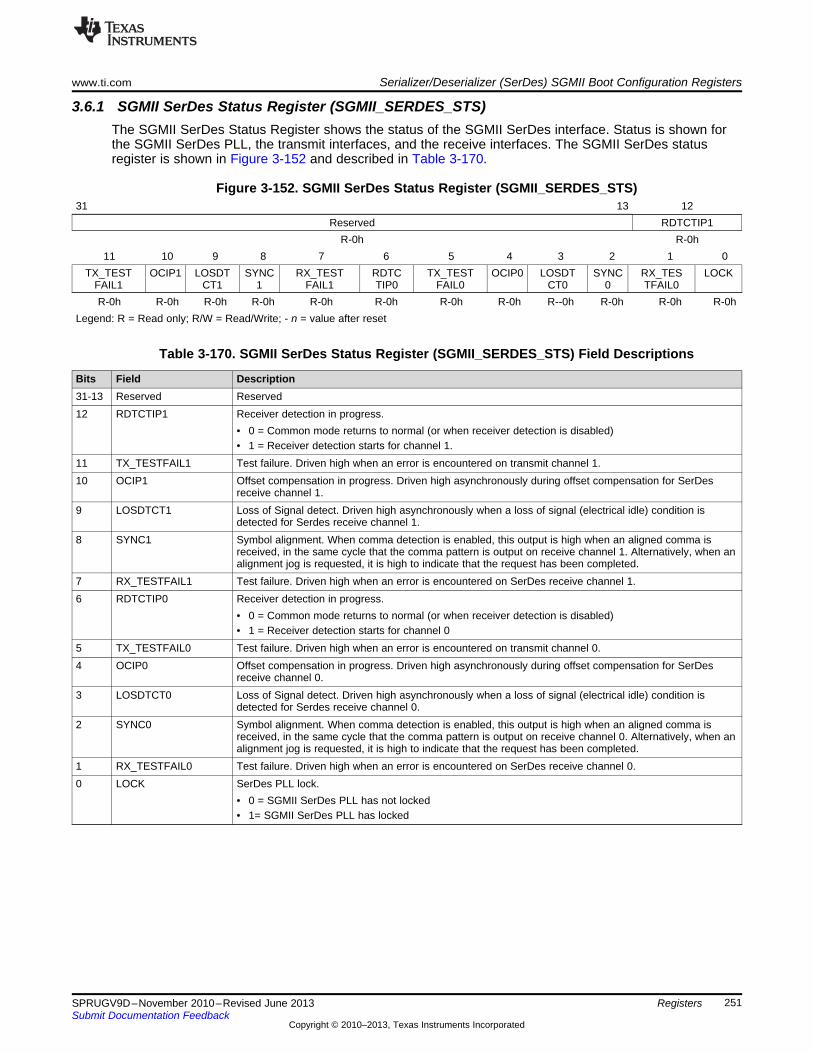
www.ti.com Serializer/Deserializer (SerDes) SGMII Boot Configuration Registers
251SPRUGV9D–November 2010–Revised June 2013Submit Documentation Feedback
Copyright © 2010–2013, Texas Instruments Incorporated
Registers
3.6.1 SGMII SerDes Status Register (SGMII_SERDES_STS)The SGMII SerDes Status Register shows the status of the SGMII SerDes interface. Status is shown forthe SGMII SerDes PLL, the transmit interfaces, and the receive interfaces. The SGMII SerDes statusregister is shown in Figure 3-152 and described in Table 3-170.
Figure 3-152. SGMII SerDes Status Register (SGMII_SERDES_STS)31 13 12
Reserved RDTCTIP1R-0h R-0h
11 10 9 8 7 6 5 4 3 2 1 0TX_TEST
FAIL1OCIP1 LOSDT
CT1SYNC
1RX_TEST
FAIL1RDTCTIP0
TX_TESTFAIL0
OCIP0 LOSDTCT0
SYNC0
RX_TESTFAIL0
LOCK
R-0h R-0h R-0h R-0h R-0h R-0h R-0h R-0h R--0h R-0h R-0h R-0hLegend: R = Read only; R/W = Read/Write; - n = value after reset
Table 3-170. SGMII SerDes Status Register (SGMII_SERDES_STS) Field Descriptions
Bits Field Description31-13 Reserved Reserved12 RDTCTIP1 Receiver detection in progress.
• 0 = Common mode returns to normal (or when receiver detection is disabled)• 1 = Receiver detection starts for channel 1.
11 TX_TESTFAIL1 Test failure. Driven high when an error is encountered on transmit channel 1.10 OCIP1 Offset compensation in progress. Driven high asynchronously during offset compensation for SerDes
receive channel 1.9 LOSDTCT1 Loss of Signal detect. Driven high asynchronously when a loss of signal (electrical idle) condition is
detected for Serdes receive channel 1.8 SYNC1 Symbol alignment. When comma detection is enabled, this output is high when an aligned comma is
received, in the same cycle that the comma pattern is output on receive channel 1. Alternatively, when analignment jog is requested, it is high to indicate that the request has been completed.
7 RX_TESTFAIL1 Test failure. Driven high when an error is encountered on SerDes receive channel 1.6 RDTCTIP0 Receiver detection in progress.
• 0 = Common mode returns to normal (or when receiver detection is disabled)• 1 = Receiver detection starts for channel 0
5 TX_TESTFAIL0 Test failure. Driven high when an error is encountered on transmit channel 0.4 OCIP0 Offset compensation in progress. Driven high asynchronously during offset compensation for SerDes
receive channel 0.3 LOSDTCT0 Loss of Signal detect. Driven high asynchronously when a loss of signal (electrical idle) condition is
detected for Serdes receive channel 0.2 SYNC0 Symbol alignment. When comma detection is enabled, this output is high when an aligned comma is
received, in the same cycle that the comma pattern is output on receive channel 0. Alternatively, when analignment jog is requested, it is high to indicate that the request has been completed.
1 RX_TESTFAIL0 Test failure. Driven high when an error is encountered on SerDes receive channel 0.0 LOCK SerDes PLL lock.
• 0 = SGMII SerDes PLL has not locked• 1= SGMII SerDes PLL has locked
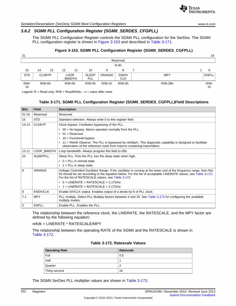
Serializer/Deserializer (SerDes) SGMII Boot Configuration Registers www.ti.com
252 SPRUGV9D–November 2010–Revised June 2013Submit Documentation Feedback
Copyright © 2010–2013, Texas Instruments Incorporated
Registers
3.6.2 SGMII PLL Configuration Register (SGMII_SERDES_CFGPLL)The SGMII PLL Configuration Register controls the SGMII PLL configuration for the SerDes. The SGMIIPLL configuration register is shown in Figure 3-153 and described in Table 3-171.
Figure 3-153. SGMII PLL Configuration Register (SGMII_SERDES_CGFPLL)31 16
ReservedR-0h
15 14 13 12 11 10 9 8 7 1 0STD CLKBYP LOOP
_BWIDTHSLEEP
PLLVRANGE ENDIV
CLKMPY ENPLL
R/W-1h
R/W-0h R/W-0h R/W-0h R/W-1h R/W-0h R/W-28h R/W-1h
Legend: R = Read only; R/W = Read/Write; - n = value after reset
Table 3-171. SGMII PLL Configuration Register (SGMII_SERDES_CGFPLL)Field Descriptions
Bits Field Description31-16 Reserved Reserved15 STD Standard selection. Always write 0 to this register field.14-13 CLKBYP Clock bypass. Facilitates bypassing of the PLL.
• 00 = No bypass. Macro operates normally from the PLL.• 01 = Reserved• 10 = Functional bypass.• 11 = Refclk Observe. The PLL is bypassed by refclkp/n. This diagnostic capability is designed to facilitate
observation of the reference clock from macros containing transmitters.12-11 LOOP_BWIDTH Loop bandwidth. Always program this field to 00b.10 SLEEPPLL Sleep PLL. Puts the PLL into the sleep state when high.
• 0 = PLL in normal state• 1 = PLL in sleep state
9 VRANGE Voltage Controlled Oscillator Range. If the oscillator is running at the lower end of the frequency range, then thisbit should be set according to the equation below. For the list of acceptable LINERATE values, see Table 3-172.For the list of RATESCALE values, see Table 3-172.• 0 = LINERATE × RATESCALE > 2.17GHz• 1 = LINERATE × RATESCALE < 2.17GHz
8 ENDIVCLK Enable DIVCLK output. Enables output of a divide by-5 of PLL clock.7-1 MPY PLL multiply. Select PLL Multiply factors between 4 and 25. See Table 3-173 for configuring the available
multiply modes.0 ENPLL Enable PLL. Enables the PLL.
The relationship between the reference clock, the LINERATE, the RATESCALE, and the MPY factor aredefined by the following equation:
refclk = LINERATE * RATESCALE/MPY
The relationship between the operating RATE of the SGMII and the RATESCALE is shown inTable 3-172.
Table 3-172. Ratescale Values
Operating Rate RatescaleFull 0.5Half 1Quarter 2Thirty-second 16
The SGMII SerDes PLL multiplier values are shown in Table 3-173.
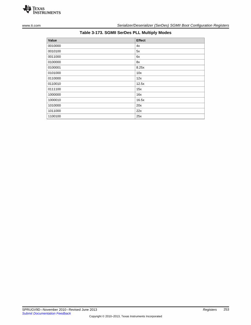
www.ti.com Serializer/Deserializer (SerDes) SGMII Boot Configuration Registers
253SPRUGV9D–November 2010–Revised June 2013Submit Documentation Feedback
Copyright © 2010–2013, Texas Instruments Incorporated
Registers
Table 3-173. SGMII SerDes PLL Multiply Modes
Value Effect0010000 4x0010100 5x0011000 6x0100000 8x0100001 8.25x0101000 10x0110000 12x0110010 12.5x0111100 15x1000000 16x1000010 16.5x1010000 20x1011000 22x1100100 25x
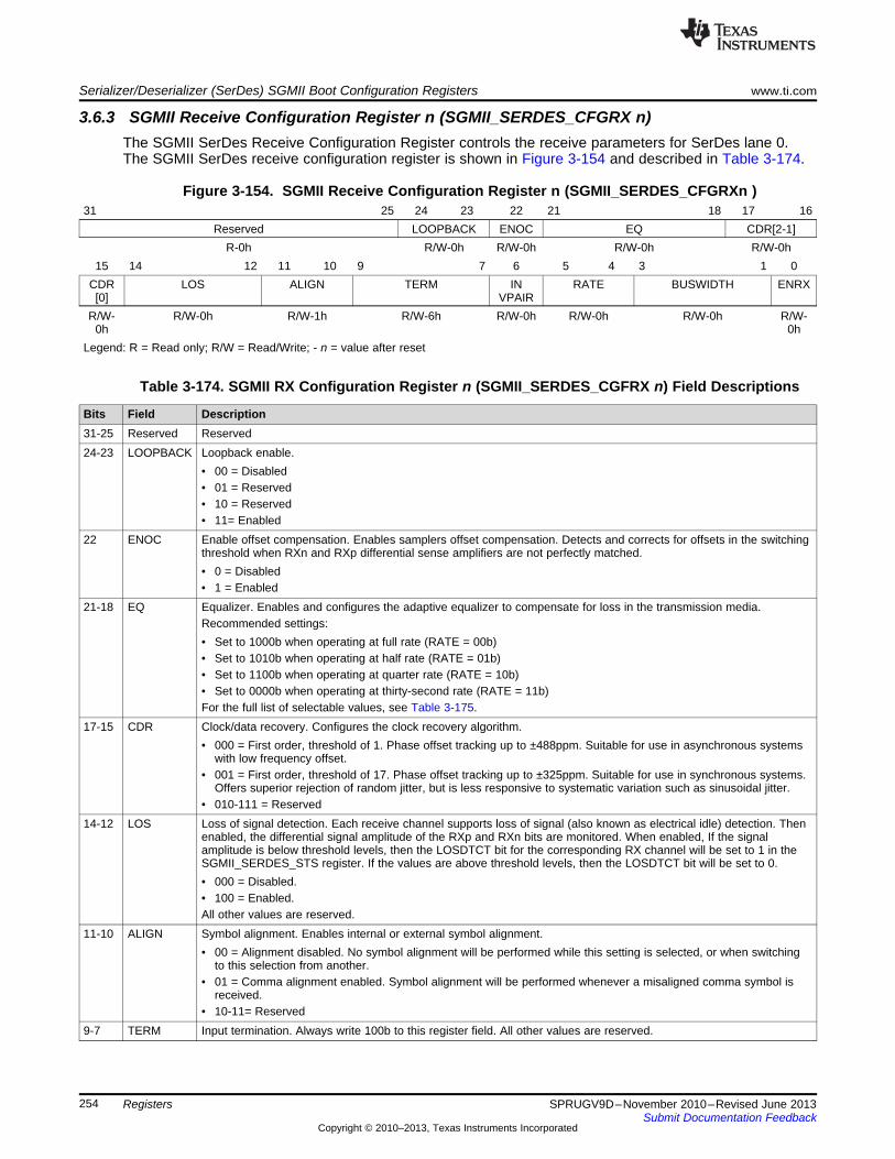
Serializer/Deserializer (SerDes) SGMII Boot Configuration Registers www.ti.com
254 SPRUGV9D–November 2010–Revised June 2013Submit Documentation Feedback
Copyright © 2010–2013, Texas Instruments Incorporated
Registers
3.6.3 SGMII Receive Configuration Register n (SGMII_SERDES_CFGRX n)The SGMII SerDes Receive Configuration Register controls the receive parameters for SerDes lane 0.The SGMII SerDes receive configuration register is shown in Figure 3-154 and described in Table 3-174.
Figure 3-154. SGMII Receive Configuration Register n (SGMII_SERDES_CFGRXn )31 25 24 23 22 21 18 17 16
Reserved LOOPBACK ENOC EQ CDR[2-1]R-0h R/W-0h R/W-0h R/W-0h R/W-0h
15 14 12 11 10 9 7 6 5 4 3 1 0CDR[0]
LOS ALIGN TERM INVPAIR
RATE BUSWIDTH ENRX
R/W-0h
R/W-0h R/W-1h R/W-6h R/W-0h R/W-0h R/W-0h R/W-0h
Legend: R = Read only; R/W = Read/Write; - n = value after reset
Table 3-174. SGMII RX Configuration Register n (SGMII_SERDES_CGFRX n) Field Descriptions
Bits Field Description31-25 Reserved Reserved24-23 LOOPBACK Loopback enable.
• 00 = Disabled• 01 = Reserved• 10 = Reserved• 11= Enabled
22 ENOC Enable offset compensation. Enables samplers offset compensation. Detects and corrects for offsets in the switchingthreshold when RXn and RXp differential sense amplifiers are not perfectly matched.• 0 = Disabled• 1 = Enabled
21-18 EQ Equalizer. Enables and configures the adaptive equalizer to compensate for loss in the transmission media.Recommended settings:• Set to 1000b when operating at full rate (RATE = 00b)• Set to 1010b when operating at half rate (RATE = 01b)• Set to 1100b when operating at quarter rate (RATE = 10b)• Set to 0000b when operating at thirty-second rate (RATE = 11b)For the full list of selectable values, see Table 3-175.
17-15 CDR Clock/data recovery. Configures the clock recovery algorithm.• 000 = First order, threshold of 1. Phase offset tracking up to ±488ppm. Suitable for use in asynchronous systems
with low frequency offset.• 001 = First order, threshold of 17. Phase offset tracking up to ±325ppm. Suitable for use in synchronous systems.
Offers superior rejection of random jitter, but is less responsive to systematic variation such as sinusoidal jitter.• 010-111 = Reserved
14-12 LOS Loss of signal detection. Each receive channel supports loss of signal (also known as electrical idle) detection. Thenenabled, the differential signal amplitude of the RXp and RXn bits are monitored. When enabled, If the signalamplitude is below threshold levels, then the LOSDTCT bit for the corresponding RX channel will be set to 1 in theSGMII_SERDES_STS register. If the values are above threshold levels, then the LOSDTCT bit will be set to 0.• 000 = Disabled.• 100 = Enabled.All other values are reserved.
11-10 ALIGN Symbol alignment. Enables internal or external symbol alignment.• 00 = Alignment disabled. No symbol alignment will be performed while this setting is selected, or when switching
to this selection from another.• 01 = Comma alignment enabled. Symbol alignment will be performed whenever a misaligned comma symbol is
received.• 10-11= Reserved
9-7 TERM Input termination. Always write 100b to this register field. All other values are reserved.
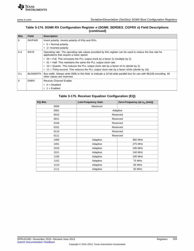
www.ti.com Serializer/Deserializer (SerDes) SGMII Boot Configuration Registers
255SPRUGV9D–November 2010–Revised June 2013Submit Documentation Feedback
Copyright © 2010–2013, Texas Instruments Incorporated
Registers
Table 3-174. SGMII RX Configuration Register n (SGMII_SERDES_CGFRX n) Field Descriptions(continued)
Bits Field Description6 INVPAIR Invert polarity. Inverts polarity of RXp and RXn.
• 0 = Normal polarity• 1= Inverted polarity
5-4 RATE Operating rate. The operating rate values provided by this register can be used to reduce the line rate forapplications that require a lower speed.• 00 = Full. This increases the PLL output clock by a factor 2x (multiply by 2).• 01 = Half. This maintains the same the PLL output clock rate.• 10 = Quarter. This reduces the PLL output clock rate by a factor of 2x (divide by 2).• 11 = Thirty-second. This reduces the PLL output clock rate by a factor of16x (divide by 16).
3-1 BUSWIDTH Bus width. Always write 000b to this field, to indicate a 10-bit-wide parallel bus for use with 8b/10b encoding. Allother values are reserved.
0 ENRX Receive Channel Enable.• 0 = Disabled• 1 = Enabled
Table 3-175. Receiver Equalizer Configuration (EQ)
EQ Bits Low-Frequency Gain Zero-Frequency (at e28 (min))0000 Maximum -0001 Adaptive0010 Reserved0011 Reserved0100 Reserved0101 Reserved0110 Reserved0111 Reserved1000 Adaptive 365 MHz1001 Adaptive 275 MHz1010 Adaptive 195 MHz1011 Adaptive 140 MHz1100 Adaptive 105 MHz1101 Adaptive 75 MHz1110 Adaptive 55 MHz1111 Adaptive 50 MHz
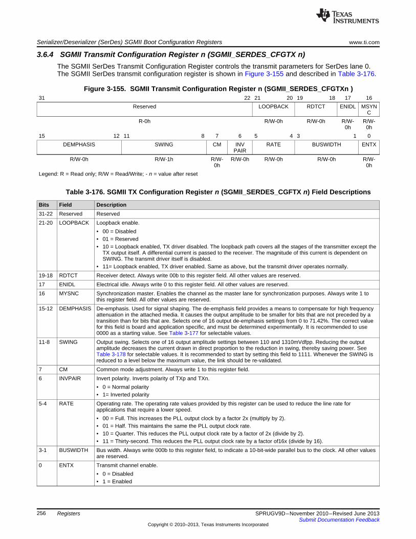
Serializer/Deserializer (SerDes) SGMII Boot Configuration Registers www.ti.com
256 SPRUGV9D–November 2010–Revised June 2013Submit Documentation Feedback
Copyright © 2010–2013, Texas Instruments Incorporated
Registers
3.6.4 SGMII Transmit Configuration Register n (SGMII_SERDES_CFGTX n)The SGMII SerDes Transmit Configuration Register controls the transmit parameters for SerDes lane 0.The SGMII SerDes transmit configuration register is shown in Figure 3-155 and described in Table 3-176.
Figure 3-155. SGMII Transmit Configuration Register n (SGMII_SERDES_CFGTXn )31 22 21 20 19 18 17 16
Reserved LOOPBACK RDTCT ENIDL MSYNC
R-0h R/W-0h R/W-0h R/W-0h
R/W-0h
15 12 11 8 7 6 5 4 3 1 0DEMPHASIS SWING CM INV
PAIRRATE BUSWIDTH ENTX
R/W-0h R/W-1h R/W-0h
R/W-0h R/W-0h R/W-0h R/W-0h
Legend: R = Read only; R/W = Read/Write; - n = value after reset
Table 3-176. SGMII TX Configuration Register n (SGMII_SERDES_CGFTX n) Field Descriptions
Bits Field Description31-22 Reserved Reserved21-20 LOOPBACK Loopback enable.
• 00 = Disabled• 01 = Reserved• 10 = Loopback enabled, TX driver disabled. The loopback path covers all the stages of the transmitter except the
TX output itself. A differential current is passed to the receiver. The magnitude of this current is dependent onSWING. The transmit driver itself is disabled.
• 11= Loopback enabled, TX driver enabled. Same as above, but the transmit driver operates normally.19-18 RDTCT Receiver detect. Always write 00b to this register field. All other values are reserved.17 ENIDL Electrical idle. Always write 0 to this register field. All other values are reserved.16 MYSNC Synchronization master. Enables the channel as the master lane for synchronization purposes. Always write 1 to
this register field. All other values are reserved.15-12 DEMPHASIS De-emphasis. Used for signal shaping. The de-emphasis field provides a means to compensate for high frequency
attenuation in the attached media. It causes the output amplitude to be smaller for bits that are not preceded by atransition than for bits that are. Selects one of 16 output de-emphasis settings from 0 to 71.42%. The correct valuefor this field is board and application specific, and must be determined experimentally. It is recommended to use0000 as a starting value. See Table 3-177 for selectable values.
11-8 SWING Output swing. Selects one of 16 output amplitude settings between 110 and 1310mVdfpp. Reducing the outputamplitude decreases the current drawn in direct proportion to the reduction in swing, thereby saving power. SeeTable 3-178 for selectable values. It is recommended to start by setting this field to 1111. Whenever the SWING isreduced to a level below the maximum value, the link should be re-validated.
7 CM Common mode adjustment. Always write 1 to this register field.6 INVPAIR Invert polarity. Inverts polarity of TXp and TXn.
• 0 = Normal polarity• 1= Inverted polarity
5-4 RATE Operating rate. The operating rate values provided by this register can be used to reduce the line rate forapplications that require a lower speed.• 00 = Full. This increases the PLL output clock by a factor 2x (multiply by 2).• 01 = Half. This maintains the same the PLL output clock rate.• 10 = Quarter. This reduces the PLL output clock rate by a factor of 2x (divide by 2).• 11 = Thirty-second. This reduces the PLL output clock rate by a factor of16x (divide by 16).
3-1 BUSWIDTH Bus width. Always write 000b to this register field, to indicate a 10-bit-wide parallel bus to the clock. All other valuesare reserved.
0 ENTX Transmit channel enable.• 0 = Disabled• 1 = Enabled
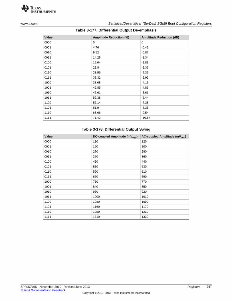
www.ti.com Serializer/Deserializer (SerDes) SGMII Boot Configuration Registers
257SPRUGV9D–November 2010–Revised June 2013Submit Documentation Feedback
Copyright © 2010–2013, Texas Instruments Incorporated
Registers
Table 3-177. Differential Output De-emphasis
Value Amplitude Reduction (%) Amplitude Reduction (dB)0000 0 00001 4.76 -0.420010 9.52 -0.870011 14.28 -1.340100 19.04 -1.830101 23.8 -2.360110 28.56 -2.360111 33.32 -2.921000 38.08 -4.161001 42.85 -4.861010 47.61 -5.611011 52.38 -6.441100 57.14 -7.351101 61.9 -8.381110 66.66 -9.541111 71.42 -10.87
Table 3-178. Differential Output Swing
Value DC-coupled Amplitude (mVdfpp) AC-coupled Amplitude (mVdfpp)0000 110 1200001 190 2000010 270 2800011 350 3600100 430 4400101 510 5300110 590 6100111 670 6901000 750 7701001 840 8501010 930 9201011 1000 10101100 1080 10901101 1160 11701110 1250 12301111 1310 1330
Revision History www.ti.com
258 SPRUGV9D–November 2010–Revised June 2013Submit Documentation Feedback
Copyright © 2010–2013, Texas Instruments Incorporated
Revision History
Revision History
Changes from August 1, 2014 to May 1, 2015 ................................................................................................................. Page
IMPORTANT NOTICE FOR TI DESIGN INFORMATION AND RESOURCES
Texas Instruments Incorporated (‘TI”) technical, application or other design advice, services or information, including, but not limited to,reference designs and materials relating to evaluation modules, (collectively, “TI Resources”) are intended to assist designers who aredeveloping applications that incorporate TI products; by downloading, accessing or using any particular TI Resource in any way, you(individually or, if you are acting on behalf of a company, your company) agree to use it solely for this purpose and subject to the terms ofthis Notice.TI’s provision of TI Resources does not expand or otherwise alter TI’s applicable published warranties or warranty disclaimers for TIproducts, and no additional obligations or liabilities arise from TI providing such TI Resources. TI reserves the right to make corrections,enhancements, improvements and other changes to its TI Resources.You understand and agree that you remain responsible for using your independent analysis, evaluation and judgment in designing yourapplications and that you have full and exclusive responsibility to assure the safety of your applications and compliance of your applications(and of all TI products used in or for your applications) with all applicable regulations, laws and other applicable requirements. Yourepresent that, with respect to your applications, you have all the necessary expertise to create and implement safeguards that (1)anticipate dangerous consequences of failures, (2) monitor failures and their consequences, and (3) lessen the likelihood of failures thatmight cause harm and take appropriate actions. You agree that prior to using or distributing any applications that include TI products, youwill thoroughly test such applications and the functionality of such TI products as used in such applications. TI has not conducted anytesting other than that specifically described in the published documentation for a particular TI Resource.You are authorized to use, copy and modify any individual TI Resource only in connection with the development of applications that includethe TI product(s) identified in such TI Resource. NO OTHER LICENSE, EXPRESS OR IMPLIED, BY ESTOPPEL OR OTHERWISE TOANY OTHER TI INTELLECTUAL PROPERTY RIGHT, AND NO LICENSE TO ANY TECHNOLOGY OR INTELLECTUAL PROPERTYRIGHT OF TI OR ANY THIRD PARTY IS GRANTED HEREIN, including but not limited to any patent right, copyright, mask work right, orother intellectual property right relating to any combination, machine, or process in which TI products or services are used. Informationregarding or referencing third-party products or services does not constitute a license to use such products or services, or a warranty orendorsement thereof. Use of TI Resources may require a license from a third party under the patents or other intellectual property of thethird party, or a license from TI under the patents or other intellectual property of TI.TI RESOURCES ARE PROVIDED “AS IS” AND WITH ALL FAULTS. TI DISCLAIMS ALL OTHER WARRANTIES ORREPRESENTATIONS, EXPRESS OR IMPLIED, REGARDING TI RESOURCES OR USE THEREOF, INCLUDING BUT NOT LIMITED TOACCURACY OR COMPLETENESS, TITLE, ANY EPIDEMIC FAILURE WARRANTY AND ANY IMPLIED WARRANTIES OFMERCHANTABILITY, FITNESS FOR A PARTICULAR PURPOSE, AND NON-INFRINGEMENT OF ANY THIRD PARTY INTELLECTUALPROPERTY RIGHTS.TI SHALL NOT BE LIABLE FOR AND SHALL NOT DEFEND OR INDEMNIFY YOU AGAINST ANY CLAIM, INCLUDING BUT NOTLIMITED TO ANY INFRINGEMENT CLAIM THAT RELATES TO OR IS BASED ON ANY COMBINATION OF PRODUCTS EVEN IFDESCRIBED IN TI RESOURCES OR OTHERWISE. IN NO EVENT SHALL TI BE LIABLE FOR ANY ACTUAL, DIRECT, SPECIAL,COLLATERAL, INDIRECT, PUNITIVE, INCIDENTAL, CONSEQUENTIAL OR EXEMPLARY DAMAGES IN CONNECTION WITH ORARISING OUT OF TI RESOURCES OR USE THEREOF, AND REGARDLESS OF WHETHER TI HAS BEEN ADVISED OF THEPOSSIBILITY OF SUCH DAMAGES.You agree to fully indemnify TI and its representatives against any damages, costs, losses, and/or liabilities arising out of your non-compliance with the terms and provisions of this Notice.This Notice applies to TI Resources. Additional terms apply to the use and purchase of certain types of materials, TI products and services.These include; without limitation, TI’s standard terms for semiconductor products http://www.ti.com/sc/docs/stdterms.htm), evaluationmodules, and samples (http://www.ti.com/sc/docs/sampterms.htm).
Mailing Address: Texas Instruments, Post Office Box 655303, Dallas, Texas 75265Copyright © 2017, Texas Instruments Incorporated