Embed Size (px)
Citation preview
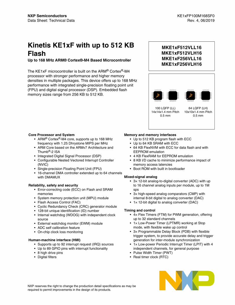
Kinetis KE1xF with up to 512 KBFlashUp to 168 MHz ARM® Cortex®-M4 Based Microcontroller
The KE1xF microcontroller is built on the ARM® Cortex®-M4processor with stronger performance and higher memorydensities in multiple packages. This device offers up to 168 MHzperformance with integrated single-precision floating point unit(FPU) and digital signal processor (DSP). Embedded flashmemory sizes range from 256 KB to 512 KB.
Core Processor and System• ARM® Cortex®-M4 core, supports up to 168 MHz
frequency with 1.25 Dhrystone MIPS per MHz• ARM Core based on the ARMv7 Architecture and
Thumb®-2 ISA• Integrated Digital Signal Processor (DSP)• Configurable Nested Vectored Interrupt Controller
(NVIC)• Single-precision Floating Point Unit (FPU)• 16-channel DMA controller extended up to 64 channels
with DMAMUX
Reliability, safety and security• Error-correcting code (ECC) on Flash and SRAM
memories• System memory protection unit (MPU) module• Flash Access Control (FAC)• Cyclic Redundancy Check (CRC) generator module• 128-bit unique identification (ID) number• Internal watchdog (WDOG) with independent clock
source• External watchdog monitor (EWM) module• ADC self calibration feature• On-chip clock loss monitoring
Human-machine interface (HMI)• Supports up to 92 interrupt request (IRQ) sources• Up to 89 GPIO pins with interrupt functionality• 8 high drive pins• Digital filters
Memory and memory interfaces• Up to 512 KB program flash with ECC• Up to 64 KB SRAM with ECC• 64 KB FlexNVM with ECC for data flash and with
EEPROM emulation• 4 KB FlexRAM for EEPROM emulation• 8 KB I/D cache to minimize performance impact of
memory access latencies• Boot ROM with built in bootloader
Mixed-signal analog• 3× 12-bit analog-to-digital converter (ADC) with up
to 16 channel analog inputs per module, up to 1Msps
• 3× high-speed analog comparators (CMP) withinternal 8-bit digital to analog converter (DAC)
• 1× 12-bit digital to analog converter (DAC)
Timing and control• 4× Flex Timers (FTM) for PWM generation, offering
up to 32 standard channels• 1× Low-Power Timer (LPTMR) working at Stop
mode, with flexible wake up control• 3× Programmable Delay Block (PDB) with flexible
trigger system, to provide accurate delay and triggergeneration for inter-module synchronization
• 1× Low-power Periodic Interrupt Timer (LPIT) with 4independent channels, for general purpose
• Pulse Width Timer (PWT)• Real timer clock (RTC)
MKE1xF512VLL16MKE1xF512VLH16MKE1xF256VLL16MKE1xF256VLH16
100 LQFP (LL)14x14x1.4 mm Pitch
0.5 mm
64 LQFP (LH)10x10x1.4 mm Pitch
0.5 mm
NXP Semiconductors KE1xFP100M168SF0Data Sheet: Technical Data Rev. 4, 06/2019
NXP reserves the right to change the production detail specifications as may berequired to permit improvements in the design of its products.
Clock interfaces• 4 - 40 MHz fast external oscillator (OSC)• 32 kHz slow external oscillator (OSC32)• 48 MHz high-accuracy (up to ±1%) fast internal
reference clock (FIRC) for high-speed run• 8 MHz / 2 MHz high-accuracy (up to ±3%) slow internal
reference clock (SIRC) for low-speed run• 128 kHz low power oscillator (LPO)• Phased lock loop (PLL)• Up to 50 MHz DC external square wave input clock• System clock generator (SCG)• Real time counter (RTC)
Power management• Low-power ARM Cortex-M4 core with excellent energy
efficiency• Power management controller (PMC) with multiple
power modes: HSRun, Run, Wait, Stop, VLPR, VLPWand VLPS
• Supports clock gating for unused modules, and specificperipherals remain working in low power modes
• POR, LVD/LVR
Operating Characteristics• Voltage range: 2.7 to 5.5 V• Ambient temperature range: –40 to 105 °C
Connectivity and communications interfaces• TriggerMUX: for module inter-connectivity• 3× low-power universal asynchronous receiver/
transmitter (LPUART) modules with DMA supportand working at Stop mode
• 2 low-power serial peripheral interface (LPSPI)modules with DMA support and working at Stopmode
• 2× low-power inter-integrated circuit (LPI2C)modules with DMA support and working at Stopmode
• Up to 2 ×FlexCAN modules, with flexible messagebuffers and mailboxes
• FlexIO module for flexible and high performanceserial interfaces emulation
Debug functionality• Serial Wire JTAG Debug Port (SWJ-DP) combines• Debug Watchpoint and Trace (DWT)• Instrumentation Trace Macrocell (ITM)• Test Port Interface Unit (TPIU)• Flash Patch and Breakpoints (FPB)
Related Resources
Type Description Resource
Product Brief The Product Brief contains concise overview/summary information toenable quick evaluation of a device for design suitability.
KE1xF512PB 1
ReferenceManual
The Reference Manual contains a comprehensive description of thestructure and function (operation) of a device.
KE1xFP100M168SF0RM 1
Data Sheet The Data Sheet includes electrical characteristics and signalconnections.
This document:
KE1xFP100M168SF0
Chip Errata The chip mask set Errata provides additional or corrective information fora particular device mask set.
Kinetis_E_0N79P 1
Packagedrawing
Package dimensions are provided in package drawings. 100-LQFP: 98ASS23308W
64-LQFP: 98ASS23234W
1. To find the associated resource, go to http://www.nxp.com and perform a search using this term.
2 Kinetis KE1xF with up to 512 KB Flash, Rev. 4, 06/2019
NXP Semiconductors
Memories and Memory Interfaces
Programflash RAM
12-bit DACx1
CRC
Analog Timers Communication InterfacesSecurityand Integrity
LPSPIx2
FlexMemory
ClocksCore
Debuginterfaces DSP
Interruptcontroller
CMP x3
LPTMR
Human-MachineInterface (HMI)
GPIO
System
eDMA
LPIT, 4ch
Boot ROM
SRTC
LPUARTx3
® CortexARM -M4®
MPU
PDB x3
DMAMUX
LPO
High drive
Digital filters
I/O (8 pins)
OSC32
upto 89
(all ports)
OSC
FIRC
SIRC
PLL
WDOG
PMC
ECC
FAC
EWM
Kinetis KE1xF Sub-Family
FPU
x2LPI C2FlexTimer
8ch x4
FlexCANupto x2
PWTFlexIO
TRGMUX
12-bit ADCx3
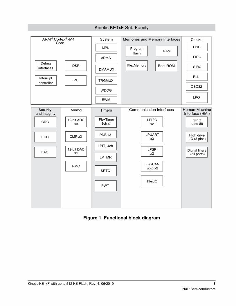
Figure 1. Functional block diagram
Kinetis KE1xF with up to 512 KB Flash, Rev. 4, 06/2019 3
NXP Semiconductors
Table of Contents
1 Ordering information............................................................... 5
2 Overview................................................................................. 5
2.1 System features...............................................................6
2.1.1 ARM Cortex-M4 core........................................ 6
2.1.2 NVIC..................................................................7
2.1.3 AWIC.................................................................7
2.1.4 Memory............................................................. 8
2.1.5 Reset and boot..................................................8
2.1.6 Clock options.....................................................10
2.1.7 Security............................................................. 11
2.1.8 Power management.......................................... 12
2.1.9 Debug controller................................................13
2.2 Peripheral features.......................................................... 14
2.2.1 eDMA and DMAMUX........................................ 14
2.2.2 FTM...................................................................14
2.2.3 ADC...................................................................15
2.2.4 DAC...................................................................15
2.2.5 CMP.................................................................. 16
2.2.6 RTC...................................................................16
2.2.7 LPIT...................................................................17
2.2.8 PDB...................................................................17
2.2.9 LPTMR.............................................................. 18
2.2.10 CRC.................................................................. 18
2.2.11 LPUART............................................................ 18
2.2.12 LPSPI................................................................ 19
2.2.13 FlexCAN............................................................19
2.2.14 LPI2C................................................................ 21
2.2.15 FlexIO................................................................21
2.2.16 Port control and GPIO.......................................22
3 Memory map........................................................................... 24
4 Pinouts.................................................................................... 26
4.1 KE1xF Signal Multiplexing and Pin Assignments............ 26
4.2 Port control and interrupt summary................................. 29
4.3 Module Signal Description Tables................................... 30
4.4 Pinout diagram................................................................ 35
4.5 Package dimensions....................................................... 37
5 Electrical characteristics..........................................................42
5.1 Terminology and guidelines.............................................42
5.1.1 Definitions......................................................... 42
5.1.2 Examples.......................................................... 42
5.1.3 Typical-value conditions....................................43
5.1.4 Relationship between ratings and operating
requirements..................................................... 43
5.1.5 Guidelines for ratings and operating
requirements..................................................... 44
5.2 Ratings............................................................................ 44
5.2.1 Thermal handling ratings...................................44
5.2.2 Moisture handling ratings.................................. 45
5.2.3 ESD handling ratings........................................ 45
5.2.4 Voltage and current operating ratings............... 45
5.3 General............................................................................46
5.3.1 Nonswitching electrical specifications............... 46
5.3.2 Switching specifications.................................... 57
5.3.3 Thermal specifications...................................... 60
5.4 Peripheral operating requirements and behaviors...........63
5.4.1 System modules................................................63
5.4.2 Clock interface modules....................................64
5.4.3 Memories and memory interfaces.....................71
5.4.4 Security and integrity modules.......................... 74
5.4.5 Analog............................................................... 74
5.4.6 Communication interfaces.................................82
5.4.7 Debug modules................................................. 86
6 Design considerations.............................................................90
6.1 Hardware design considerations..................................... 90
6.1.1 Printed circuit board recommendations.............90
6.1.2 Power delivery system...................................... 91
6.1.3 Analog design................................................... 91
6.1.4 Digital design.....................................................92
6.1.5 Crystal oscillator................................................95
6.2 Software considerations.................................................. 96
7 Part identification.....................................................................97
7.1 Description.......................................................................97
7.2 Format............................................................................. 97
7.3 Fields............................................................................... 97
7.4 Example...........................................................................97
8 Revision history.......................................................................98
4 Kinetis KE1xF with up to 512 KB Flash, Rev. 4, 06/2019
NXP Semiconductors
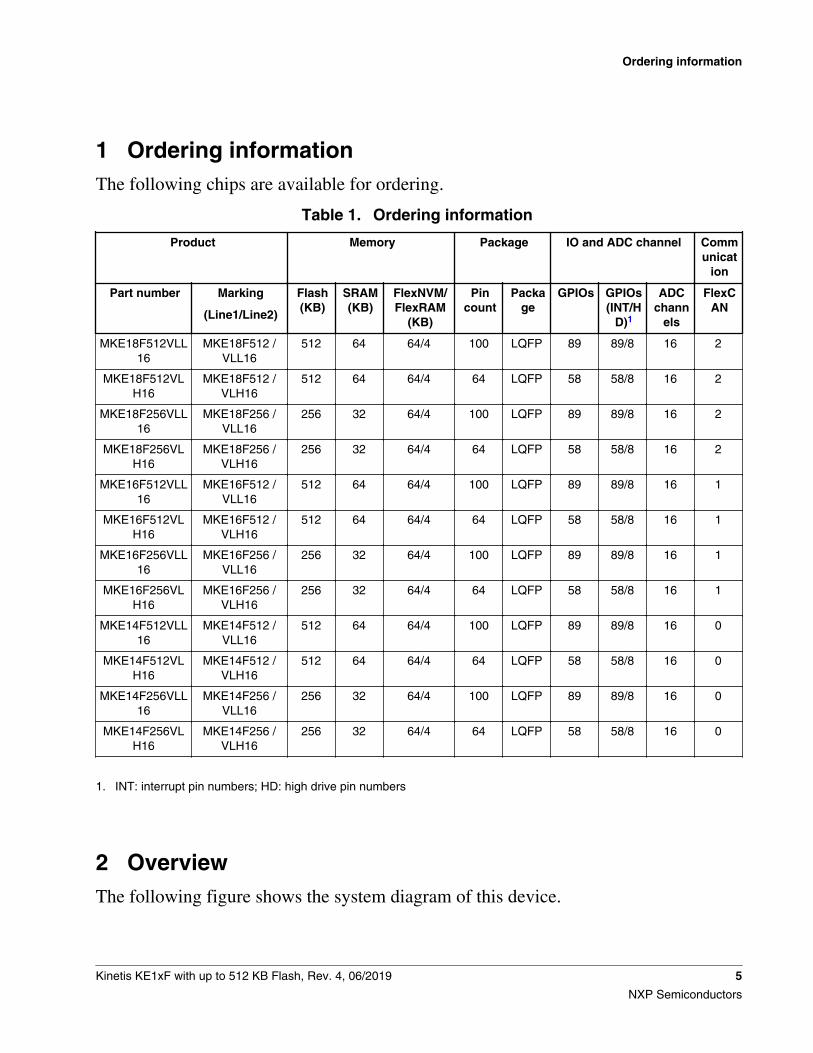
1 Ordering informationThe following chips are available for ordering.
Table 1. Ordering information
Product Memory Package IO and ADC channel Communicat
ion
Part number Marking
(Line1/Line2)
Flash(KB)
SRAM(KB)
FlexNVM/FlexRAM
(KB)
Pincount
Package
GPIOs GPIOs(INT/H
D)1
ADCchann
els
FlexCAN
MKE18F512VLL16
MKE18F512 /VLL16
512 64 64/4 100 LQFP 89 89/8 16 2
MKE18F512VLH16
MKE18F512 /VLH16
512 64 64/4 64 LQFP 58 58/8 16 2
MKE18F256VLL16
MKE18F256 /VLL16
256 32 64/4 100 LQFP 89 89/8 16 2
MKE18F256VLH16
MKE18F256 /VLH16
256 32 64/4 64 LQFP 58 58/8 16 2
MKE16F512VLL16
MKE16F512 /VLL16
512 64 64/4 100 LQFP 89 89/8 16 1
MKE16F512VLH16
MKE16F512 /VLH16
512 64 64/4 64 LQFP 58 58/8 16 1
MKE16F256VLL16
MKE16F256 /VLL16
256 32 64/4 100 LQFP 89 89/8 16 1
MKE16F256VLH16
MKE16F256 /VLH16
256 32 64/4 64 LQFP 58 58/8 16 1
MKE14F512VLL16
MKE14F512 /VLL16
512 64 64/4 100 LQFP 89 89/8 16 0
MKE14F512VLH16
MKE14F512 /VLH16
512 64 64/4 64 LQFP 58 58/8 16 0
MKE14F256VLL16
MKE14F256 /VLL16
256 32 64/4 100 LQFP 89 89/8 16 0
MKE14F256VLH16
MKE14F256 /VLH16
256 32 64/4 64 LQFP 58 58/8 16 0
1. INT: interrupt pin numbers; HD: high drive pin numbers
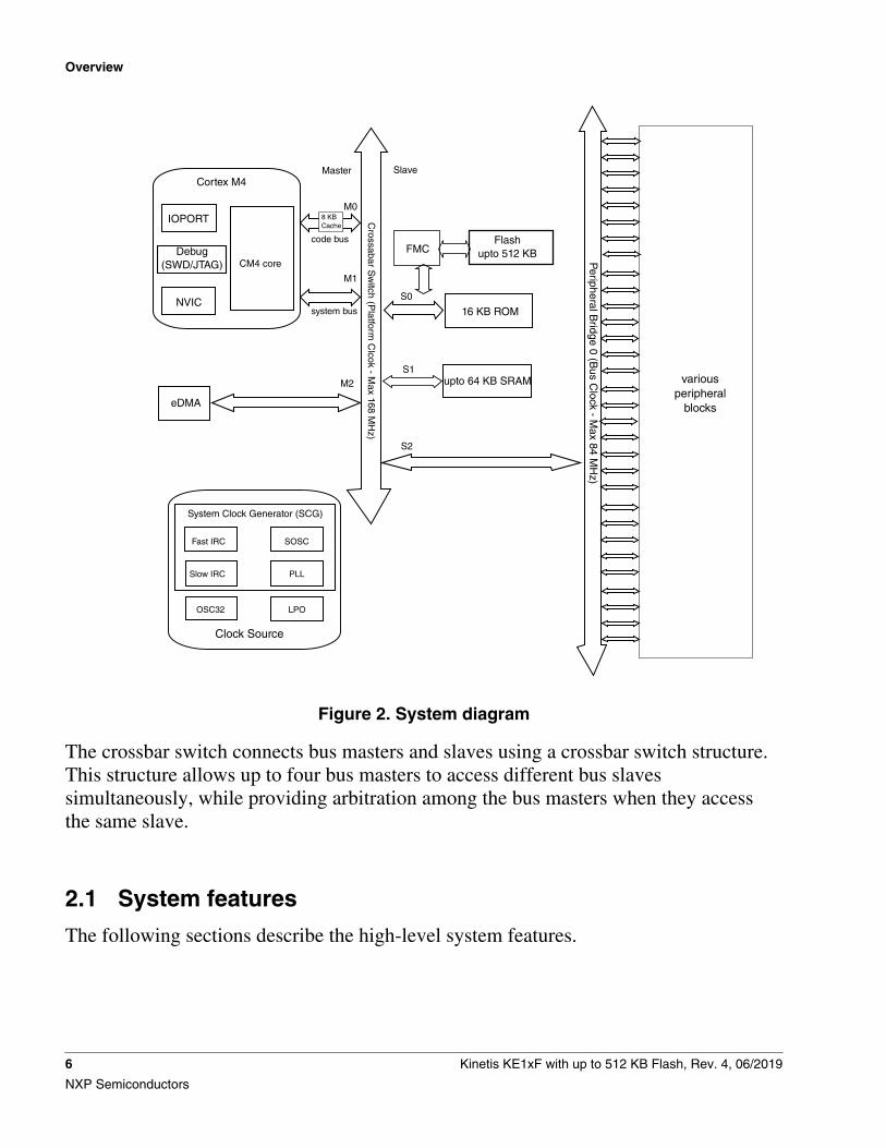
2 OverviewThe following figure shows the system diagram of this device.
Ordering information
Kinetis KE1xF with up to 512 KB Flash, Rev. 4, 06/2019 5
NXP Semiconductors
upto 64 KB SRAM
16 KB ROM
eDMA
IOPORT
Fast IRC
Slow IRC
OSC32 LPO
Flashupto 512 KB
Cortex M4
CM4 core
Crossabar S
witch (P
latform C
lcok - Max 168 M
Hz)
M0
M2
S2
S1
S0
Master Slave
System Clock Generator (SCG)
Peripheral B
ridge 0 (Bus C
lock - Max 84 M
Hz)
NVIC
M1
SOSC
PLL
code bus
system bus
variousperipheral
blocks
FMC
Clock Source
Debug(SWD/JTAG)
8 KBCache
Figure 2. System diagram
The crossbar switch connects bus masters and slaves using a crossbar switch structure.This structure allows up to four bus masters to access different bus slavessimultaneously, while providing arbitration among the bus masters when they accessthe same slave.
2.1 System features
The following sections describe the high-level system features.
Overview
6 Kinetis KE1xF with up to 512 KB Flash, Rev. 4, 06/2019
NXP Semiconductors
2.1.1 ARM Cortex-M4 core
The ARM Cortex-M4 is the member of the Cortex M Series of processors targetingmicrocontroller cores focused on very cost sensitive, deterministic, interrupt drivenenvironments. The Cortex M4 processor is based on the ARMv7 Architecture andThumb®-2 ISA and is upward compatible with the Cortex M3, Cortex M1, andCortex M0 architectures. Cortex M4 improvements include an ARMv7 Thumb-2 DSP(ported from the ARMv7-A/R profile architectures) providing 32-bit instructions withSIMD (single instruction multiple data) DSP style multiply-accumulates andsaturating arithmetic.
2.1.2 NVIC
The Nested Vectored Interrupt Controller supports nested interrupts and 16 prioritylevels for interrupts. In the NVIC, each source in the IPR registers contains 4 bits. Italso differs in number of interrupt sources and supports 240 interrupt vectors.
The Cortex-M family uses a number of methods to improve interrupt latency . It alsocan be used to wake the MCU core from Wait and VLPW modes.
2.1.3 AWIC
The asynchronous wake-up interrupt controller (AWIC) is used to detectasynchronous wake-up events in Stop mode and signal to clock control logic toresume system clocking. After clock restarts, the NVIC observes the pending interruptand performs the normal interrupt or event processing. The AWIC can be used towake MCU core from Partial Stop, Stop and VLPS modes.
Wake-up sources for this SoC are listed as below:
Table 2. AWIC Stop and VLPS Wake-up Sources
Wake-up source Description
Available system resets RESET pin, WDOG, JTAG , loss of clock(LOC) reset and loss of lock (LOL) reset
Pin interrupts Port Control Module - Any enabled pin interrupt is capable of waking the system
ADCx ADCx is optional functional with clock source from SIRC or OSC
CMPx Functional in Stop/VLPS modes with clock source from SIRC or OSC
LPI2C Functional in Stop/VLPS modes with clock source from SIRC or OSC
LPUART Functional in Stop/VLPS modes with clock source from SIRC or OSC
LPSPI Functional in Stop/VLPS modes with clock source from SIRC or OSC
Table continues on the next page...
Overview
Kinetis KE1xF with up to 512 KB Flash, Rev. 4, 06/2019 7
NXP Semiconductors
Table 2. AWIC Stop and VLPS Wake-up Sources (continued)
Wake-up source Description
LPIT Functional in Stop/VLPS modes with clock source from SIRC or OSC
FlexIO Functional in Stop/VLPS modes with clock source from SIRC or OSC
LPTMR Functional in Stop/VLPS modes
RTC Functional in Stop/VLPS modes
SCG Functional in Stop mode (Only SIRC)
CAN CAN stop wakeup
NMI Non-maskable interrupt
2.1.4 MemoryThis device has the following features:
• Upto 512 KB of embedded program flash memory.• Upto 64 KB of embedded SRAM accessible (read/write) at CPU clock speed with 0
wait states.• The non-volatile memory is divided into several arrays:
• 64 KB of embedded data flash memory• 4 KB of Emulated EEPROM• 16 KB ROM (built-in bootloader to support UART, I2C, and SPI interfaces)
The program flash memory contains a 16-byte flash configuration field that storesdefault protection settings and security information. The page size of program flashis 4 KB.
The protection setting can protect 32 regions of the program flash memory fromunintended erase or program operations.
The security circuitry prevents unauthorized access to RAM or flash contents fromdebug port.
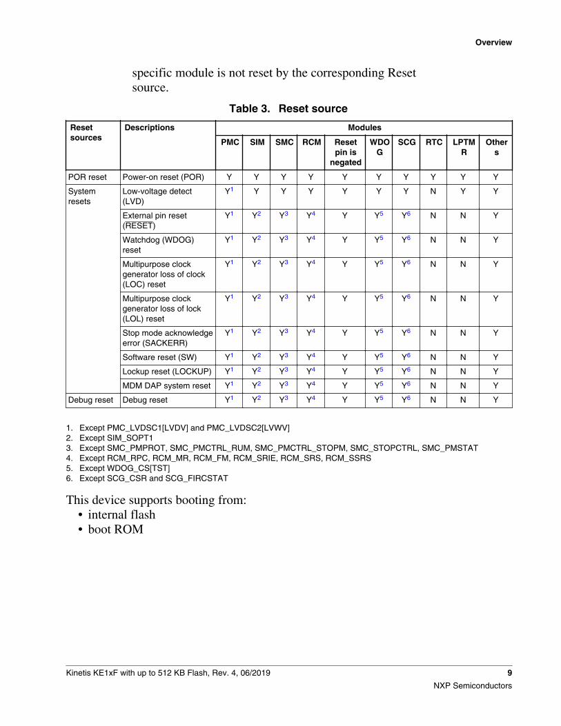
2.1.5 Reset and boot
The following table lists all the reset sources supported by this device.
NOTEIn the following table, Y means the specific module, exceptfor the registers, bits or conditions mentioned in the footnote,is reset by the corresponding Reset source. N means the
Overview
8 Kinetis KE1xF with up to 512 KB Flash, Rev. 4, 06/2019
NXP Semiconductors
specific module is not reset by the corresponding Resetsource.
Table 3. Reset source
Resetsources
Descriptions Modules
PMC SIM SMC RCM Resetpin is
negated
WDOG
SCG RTC LPTMR
Others
POR reset Power-on reset (POR) Y Y Y Y Y Y Y Y Y Y
Systemresets
Low-voltage detect(LVD)
Y1 Y Y Y Y Y Y N Y Y
External pin reset(RESET)
Y1 Y2 Y3 Y4 Y Y5 Y6 N N Y
Watchdog (WDOG)reset
Y1 Y2 Y3 Y4 Y Y5 Y6 N N Y
Multipurpose clockgenerator loss of clock(LOC) reset
Y1 Y2 Y3 Y4 Y Y5 Y6 N N Y
Multipurpose clockgenerator loss of lock(LOL) reset
Y1 Y2 Y3 Y4 Y Y5 Y6 N N Y
Stop mode acknowledgeerror (SACKERR)
Y1 Y2 Y3 Y4 Y Y5 Y6 N N Y
Software reset (SW) Y1 Y2 Y3 Y4 Y Y5 Y6 N N Y
Lockup reset (LOCKUP) Y1 Y2 Y3 Y4 Y Y5 Y6 N N Y
MDM DAP system reset Y1 Y2 Y3 Y4 Y Y5 Y6 N N Y
Debug reset Debug reset Y1 Y2 Y3 Y4 Y Y5 Y6 N N Y
1. Except PMC_LVDSC1[LVDV] and PMC_LVDSC2[LVWV]2. Except SIM_SOPT13. Except SMC_PMPROT, SMC_PMCTRL_RUM, SMC_PMCTRL_STOPM, SMC_STOPCTRL, SMC_PMSTAT4. Except RCM_RPC, RCM_MR, RCM_FM, RCM_SRIE, RCM_SRS, RCM_SSRS5. Except WDOG_CS[TST]6. Except SCG_CSR and SCG_FIRCSTAT
This device supports booting from:• internal flash• boot ROM
Overview
Kinetis KE1xF with up to 512 KB Flash, Rev. 4, 06/2019 9
NXP Semiconductors
Boot from FlashBoot from ROM
POR or Reset
RCM[FORCEROM] =00
FOPT[BOOTPIN_OPT]=0
BOOTCFG0 pin=0
FOPT[BOOTSRC _SEL]=10/11
N
N
N
Y
N
Y
Y
Y
Figure 3. Boot flow chart
The blank chip is default to boot from ROM and remaps the vector table to ROM baseaddress, otherwise, it remaps to flash address.
2.1.6 Clock options
The SCG module controls which clock source is used to derive the system clocks. Theclock generation logic divides the selected clock source into a variety of clock domains,including the clocks for the system bus masters, system bus slaves, and flash memory .The clock generation logic also implements module-specific clock gating to allowgranular shutoff of modules.
The following figure is a high level block diagram of the clock generation. For moredetails on the clock operation and configuration, see the Clocking chapter in theReference Manual.
Overview
10 Kinetis KE1xF with up to 512 KB Flash, Rev. 4, 06/2019
NXP Semiconductors
Peripheral Registers
Fast
Slow
OSC
EXTAL
XTAL
PLL
DIVCORE
SIRCDIV1_CLK
FIRCDIV1_CLK
SOSCDIV1_CLK
SCG
PLLDIV1_CLK
RTC_CLKIN
PMC
OSC
48 MHz
8MHz/2MHz
PREDIVIRC
IRC
default start up
DIVBUS
High Range
OSC
EXTAL32
XTAL32
Low RangeCLKOUT
OSC32
LPO128K
LPO_CLK
PCC
Core RAM
BUS_CLK
BUSOUT
PCC_xxx[CGC]
OSC32_CLK
CLKOUTDIV
SCG CLKOUT
PLLDIV1
FIRCDIV1
SOSCDIV1
PCC_xxx[PCS]
Async clock
WDOG
LPTMR
GPIOC
CORE_CLK/SYS_CLK
SYS_CLK
ADCxFlexIOLPIT
LPI2CxLPUARTx
LPSPIx
RTC_CLKOUT32kHz
1kHz RTC
÷128
PORT Control
CRC8-bit DACACMPx
DMAMUXeDMA
PDB
TCLK2
TCLK1
TCLK0
FTMx
PWT
SCG_xCCR[SCS]
PLL_CLK
SIRC_CLK
FIRC_CLK
SOSC_CLK
SIM_CHIPCTL[CLKOUTSEL]
RTC_CR[LPOS]
SIM_CHIPCTL[RTC_CLKSEL]
SCG_CLKOUTCNFG[CLKOUTSEL]
OSC32_CR[ROSCEREFS]
SCG_SOSCCFG[EREFS]
(SCG_SPLLCFG)
SCG_SPLLCFG[SOURCE]
SIM_FTMOPT0[FTMxCLKSEL]
SIM_CHIPCTL[PWT_CLKSEL]
0
1
00011011
0
10001 0011 0010 0110Other
01
00
10
11
0
1
0110
0011
0010
0001
Other
1
0
00
01
10
11
00
01
10
11
(x=R, V, H)
DIVSLOWFLASH_CLK
Flash
PLLDIV2
SIRCDIV2
SIRCDIV1
FIRCDIV2
SOSCDIV2SOSCDIV2_CLK
FIRCDIV2_CLK
SIRCDIV2_CLK
PLLDIV2_CLK
12-bit DAC
FlexCANx
÷2
0000
EWM
Figure 4. Clocking block diagram
2.1.7 Security
Security state can be enabled via programming flash configure field (0x40e). Afterenabling device security, the SWD/JTAG port cannot access the memory resources ofthe MCU.
External interface Security Unsecure
SWD/JTAG port Can't access memory source by SWD/JTAG interface
the debugger can write to the FlashMass Erase in Progress field of theMDM-AP Control register to trigger amass erase (Erase All Blocks)command
2.1.7.1 Flash Access Control (FAC)
The FAC is a native or third-party configurable memory protection scheme optimizedto allow end users to utilize software libraries while offering programmablerestrictions to these libraries. The flash memory is divided into equal size segmentsthat provide protection to proprietary software libraries. The protection of these
Overview
Kinetis KE1xF with up to 512 KB Flash, Rev. 4, 06/2019 11
NXP Semiconductors
segments is controlled as the FAC provides a cycle-by-cycle evaluation of the accessrights for each transaction routed to the on-chip flash memory. Configurability allowsan increasing number of protected segments while supporting two levels of vendorsadding their proprietary software to a device.
2.1.7.2 Error-correcting code (ECC)
The ECC detection is also supported on Flash and SRAM memories. It supports autocorrection of one-bit error and reporting more than one-bit error.
2.1.8 Power management
The Power Management Controller (PMC) expands upon ARM’s operational modes ofRun, Sleep, and Deep Sleep, to provide multiple configurable modes. These modes canbe used to optimize current consumption for a wide range of applications. The WFI orWFE instruction invokes a Wait or a Stop mode, depending on the currentconfiguration. For more information on ARM’s operational modes, See the ARM®
Cortex® User Guide.
The PMC provides High Speed Run (HSRUN), Normal Run (RUN), and Very LowPower Run (VLPR) configurations in ARM’s Run operation mode. In these modes, theMCU core is active and can access all peripherals. The difference between the modes isthe maximum clock frequency of the system and therefore the power consumption. Theconfiguration that matches the power versus performance requirements of theapplication can be selected.
The PMC provides Wait (Wait) and Very Low Power Wait (VLPW) configurations inARM’s Sleep operation mode. In these modes, even though the MCU core is inactive,all of the peripherals can be enabled and operate as programmed. The differencebetween the modes is the maximum clock frequency of the system and therefore thepower consumption.
The PMC provides Stop (Stop), Very Low Power Stop (VLPS) configurations inARM’s Deep Sleep operational mode. In these modes, the MCU core and most of theperipherals are disabled. Depending on the requirements of the application, differentportions of the analog, logic, and memory can be retained or disabled to conservepower.
Overview
12 Kinetis KE1xF with up to 512 KB Flash, Rev. 4, 06/2019
NXP Semiconductors
The Nested Vectored Interrupt Controller (NVIC), the Asynchronous Wake-upInterrupt Controller (AWIC) are used to wake up the MCU from low power states.The NVIC is used to wake up the MCU core from WAIT and VLPW modes. TheAWIC is used to wake up the MCU core from STOP and VLPS modes.
For additional information regarding operational modes, power management, theNVIC, AWIC, please refer to the Reference Manual.
The following table provides information about the state of the peripherals in thevarious operational modes and the modules that can wake MCU from low powermodes.
Table 5. Peripherals states in different operational modes
Core mode Device mode Descriptions
Run mode High Speed Run In HSRun mode, MCU is able to operate at a faster frequency, and all devicemodules are operational.
Run In Run mode, all device modules are operational.
Very Low Power Run In VLPR mode, all device modules are operational at a reduced frequencyexcept the Low Voltage Detect (LVD) monitor, which is disabled.
Sleep mode Wait In Wait mode, all peripheral modules are operational. The MCU core isplaced into Sleep mode.
Very Low Power Wait In VLPW mode, all peripheral modules are operational at a reducedfrequency except the Low Voltage Detect (LVD) monitor, which is disabled.The MCU core is placed into Sleep mode.
Deep sleep Stop In Stop mode, most peripheral clocks are disabled and placed in a staticstate. Stop mode retains all registers and SRAMs while maintaining LowVoltage Detection protection. In Stop mode, the ADC, DAC, CMP, LPTMR,RTC, and pin interrupts are operational. The NVIC is disabled, but the AWICcan be used to wake up from an interrupt.
Very Low Power Stop In VLPS mode, the contents of the SRAM are retained. The CMP (lowspeed), ADC, OSC, RTC, LPTMR, LPIT, FlexIO, LPUART, LPI2C,LPSPI,and DMA are operational, LVD and NVIC are disabled, AWIC is used towake up from interrupt.
NOTEWhen the MCU is in HSRUN or VLP mode, user cannotwrite FlexRAM (EEPROM), and cannot launch an FTFEcommand including flash programming/erasing.
2.1.9 Debug controller
This device has extensive debug capabilities including run control and tracingcapabilities. The standard ARM debug port supports SWD/JTAG interface.
Overview
Kinetis KE1xF with up to 512 KB Flash, Rev. 4, 06/2019 13
NXP Semiconductors
2.2 Peripheral features
The following sections describe the features of each peripherals of the chip.
2.2.1 eDMA and DMAMUX
The eDMA is a highly programmable data-transfer engine optimized to minimize anyrequired intervention from the host processor. It is intended for use in applicationswhere the data size to be transferred is statically known and not defined within thetransferred data itself. The DMA controller in this device implements 16 channelswhich can be routed from up to 63 DMA request sources through DMA MUX module.
Main features of eDMA are listed below:• All data movement via dual-address transfers: read from source, write to
destination• 16-channel implementation that performs complex data transfers with minimal
intervention from a host processor• Transfer control descriptor (TCD) organized to support two-deep, nested transfer
operations• Channel activation via one of three methods• Fixed-priority and round-robin channel arbitration• Channel completion reported via programmable interrupt requests• Programmable support for scatter/gather DMA processing• Support for complex data structures
2.2.2 FTM
This device contains four FlexTimer modules.
The FlexTimer module (FTM) is a two-to-eight channel timer that supports inputcapture, output compare, and the generation of PWM signals to control electric motorand power management applications. The FTM time reference is a 16-bit counter thatcan be used as an unsigned or signed counter.
Several key enhancements of this module are made:• Signed up counter• Deadtime insertion hardware• Fault control inputs
Overview
14 Kinetis KE1xF with up to 512 KB Flash, Rev. 4, 06/2019
NXP Semiconductors
• Enhanced triggering functionality• Initialization and polarity control
2.2.3 ADC
This device contains three 12-bit SAR ADC modules. The ADC module supportshardware triggers from FTM, LPTMR, PIT, RTC, external trigger pin and CMPoutput. It supports wakeup of MCU in low power mode when using internal clocksource or external crystal clock.
ADC module has the following features:• Linear successive approximation algorithm with up to 12-bit resolution• Up to 16 single-ended external analog inputs• Support 12-bit, 10-bit, and 8-bit single-ended output modes• Single or continuous conversion• Configurable sample time and conversion speed/power• Input clock selectable from up to four sources• Operation in low-power modes for lower noise• Selectable hardware conversion trigger• Automatic compare with interrupt for less-than, greater-than or equal-to, within
range, or out-of-range, programmable value• Temperature sensor• Hardware average function• Selectable Voltage reference: from external or alternate• Self-Calibration mode
2.2.3.1 Temperature sensor
This device contains one temperature sensor internally connected to the input channelof AD26, see ADC electrical characteristics for details of the linearity factor.
The sensor must be calibrated to gain good accuracy, so as to provide good linearity,see also AN3031 for more detailed application information of the temperature sensor.
2.2.4 DAC
The 12-bit digital-to-analog converter (DAC) is a low-power, general-purpose DAC.The output of the DAC can be placed on an external pin or set as one of the inputs tothe analog comparator, or ADC.
Overview
Kinetis KE1xF with up to 512 KB Flash, Rev. 4, 06/2019 15
NXP Semiconductors
DAC module has the following features:• On-chip programmable reference generator output. The voltage output range is
from 1⁄4096 Vin to Vin, and the step is 1⁄4096 Vin, where Vin is the input voltage.• Vin can be selected from two reference sources• Static operation in Normal Stop mode• 16-word data buffer supported with multiple operation modes• DMA support
2.2.5 CMPThere are three analog comparators on this device.
• Each CMP has its own independent 8-bit DAC.• Each CMP supports up to 7 analog inputs from external pins.• Each CMP is able to convert an internal reference from the bandgap.• Each CMP supports internal reference from the on-chip 12-bit DAC out.• Each CMP supports the round-robin sampling scheme. In summary, this allow the
CMP to operate independently in VLPS and Stop modes, whilst being triggeredperiodically to sample up to 8 inputs. Only if an input changes state is a full wakeupgenerated.
The CMP has the following features:• Inputs may range from rail to rail• Programmable hysteresis control• Selectable interrupt on rising-edge, falling-edge, or both rising and falling edges of
the comparator output• Selectable inversion on comparator output• Capability to produce a wide range of outputs such as sampled, windowed, or
digitally filtered• External hysteresis can be used at the same time that the output filter is used for
internal functions• Two software selectable performance levels: Shorter propagation delay at the
expense of higher power, and Low power with longer propagation delay• DMA transfer support• Functional in all power modes available on this MCU• The window and filter functions are not available in STOP mode• Integrated 8-bit DAC with selectable supply reference source and can be power
down to conserve power
Overview
16 Kinetis KE1xF with up to 512 KB Flash, Rev. 4, 06/2019
NXP Semiconductors
2.2.6 RTC
The RTC is an always powered-on block that remains active in all low power modes.The time counter within the RTC is clocked by a 32.768 kHz clock sourced from anexternal crystal using the oscillator, or clock directly from RTC_CLKIN pin.
RTC is reset on power-on reset, and a software reset bit in RTC can also initialize allRTC registers.
The RTC module has the following features• 32-bit seconds counter with roll-over protection and 32-bit alarm• 16-bit prescaler with compensation that can correct errors between 0.12 ppm and
3906 ppm• Register write protection with register lock mechanism• 1 Hz square wave or second pulse output with optional interrupt
2.2.7 LPIT
The Low Power Periodic Interrupt Timer (LPIT) is a multi-channel timer modulegenerating independent pre-trigger and trigger outputs. These timer channels canoperate individually or can be chained together. The LPIT can operate in low powermodes if configured to do so. The pre-trigger and trigger outputs can be used totrigger other modules on the device.
This device contains one LPIT module with four channels. The LPIT generatesperiodic trigger events to the DMAMUX.
2.2.8 PDB
The Programmable Delay Block (PDB) provides controllable delays from either aninternal or an external trigger, or a programmable interval tick, to the hardware triggerinputs of ADCs and/or generates the interval triggers to DACs, so that the precisetiming between ADC conversions and/or DAC updates can be achieved. The PDB canoptionally provide pulse outputs (Pulse-Out's) that are used as the sample window inthe CMP block.
The PDB module has the following capabilities:• trigger input sources and one software trigger source• 1 DAC refresh trigger output, for this device• configurable PDB channels for ADC hardware trigger• 1 pulse output, for this device
Overview
Kinetis KE1xF with up to 512 KB Flash, Rev. 4, 06/2019 17
NXP Semiconductors
2.2.9 LPTMR
The low-power timer (LPTMR) can be configured to operate as a time counter withoptional prescaler, or as a pulse counter with optional glitch filter, across all powermodes, including the low-leakage modes. It can also continue operating through mostsystem reset events, allowing it to be used as a time of day counter.
The LPTMR module has the following features:• 16-bit time counter or pulse counter with compare
• Optional interrupt can generate asynchronous wakeup from any low-powermode
• Hardware trigger output• Counter supports free-running mode or reset on compare
• Configurable clock source for prescaler/glitch filter• Configurable input source for pulse counter
2.2.10 CRC
This device contains one cyclic redundancy check (CRC) module which can generate16/32-bit CRC code for error detection.
The CRC module provides a programmable polynomial, WAS, and other parametersrequired to implement a 16-bit or 32-bit CRC standard.
The CRC module has the following features:• Hardware CRC generator circuit using a 16-bit or 32-bit programmable shift
register• Programmable initial seed value and polynomial• Option to transpose input data or output data (the CRC result) bitwise or bytewise.• Option for inversion of final CRC result• 32-bit CPU register programming interface
2.2.11 LPUART
This product contains three Low-Power UART modules, and can work in Stop andVLPS modes. The module also supports 4× to 32× data oversampling rate to meetdifferent applications.
The LPUART module has the following features:
Overview
18 Kinetis KE1xF with up to 512 KB Flash, Rev. 4, 06/2019
NXP Semiconductors
• Programmable baud rates (13-bit modulo divider) with configurable oversamplingratio from 4× to 32×
• Transmit and receive baud rate can operate asynchronous to the bus clock and canbe configured independently of the bus clock frequency, support operation in Stopmode
• Interrupt, DMA or polled operation• Hardware parity generation and checking• Programmable 8-bit, 9-bit or 10-bit character length• Programmable 1-bit or 2-bit stop bits• Three receiver wakeup methods
• Idle line wakeup• Address mark wakeup• Receive data match
• Automatic address matching to reduce ISR overhead:• Address mark matching• Idle line address matching• Address match start, address match end
• Optional 13-bit break character generation / 11-bit break character detection• Configurable idle length detection supporting 1, 2, 4, 8, 16, 32, 64 or 128 idle
characters• Selectable transmitter output and receiver input polarity
2.2.12 LPSPI
This device contains two LPSPI modules. The LPSPI is a low power Serial PeripheralInterface (SPI) module that supports an efficient interface to an SPI bus as a masterand/or a slave. The LPSPI can continue operating in stop modes provided anappropriate clock is available and is designed for low CPU overhead with DMAoffloading of FIFO register accesses.
The LPSPI modules have the following features:• Command/transmit FIFO of 4 words• Receive FIFO of 4 words• Host request input can be used to control the start time of an SPI bus transfer
Overview
Kinetis KE1xF with up to 512 KB Flash, Rev. 4, 06/2019 19
NXP Semiconductors
2.2.13 FlexCAN
This device contains two FlexCAN modules. The FlexCAN module is a communicationcontroller implementing the CAN protocol according to the ISO 11898-1 standard andCAN 2.0 B protocol specifications.
Each FlexCAN module contains 16 message buffers. Each message buffer is 16 bytes.
The FlexCAN module has the following features:• Flexible mailboxes of zero to eight bytes data length• Each mailbox configurable as receive or transmit, all supporting standard and
extended messages• Individual Rx Mask registers per mailbox• Full-featured Rx FIFO with storage capacity for up to six frames and automatic
internal pointer handling with DMA support• Transmission abort capability• Programmable clock source to the CAN Protocol Interface, either peripheral clock
or oscillator clock• RAM not used by reception or transmission structures can be used as general
purpose RAM space• Listen-Only mode capability• Programmable Loop-Back mode supporting self-test operation• Programmable transmission priority scheme: lowest ID, lowest buffer number, or
highest priority• Time stamp based on 16-bit free-running timer• Global network time, synchronized by a specific message• Maskable interrupts• Independence from the transmission medium (an external transceiver is assumed)• Short latency time due to an arbitration scheme for high-priority messages• Low power modes, with programmable wake up on bus activity• Remote request frames may be handled automatically or by software• CAN bit time settings and configuration bits can only be written in Freeze mode• Tx mailbox status (Lowest priority buffer or empty buffer)• Identifier Acceptance Filter Hit Indicator (IDHIT) register for received frames• SYNCH bit available in Error in Status 1 register to inform that the module is
synchronous with CAN bus• CRC status for transmitted message• Rx FIFO Global Mask register
Overview
20 Kinetis KE1xF with up to 512 KB Flash, Rev. 4, 06/2019
NXP Semiconductors
• Selectable priority between mailboxes and Rx FIFO during matching process• Powerful Rx FIFO ID filtering, capable of matching incoming IDs against either
128 extended, 256 standard, or 512 partial (8 bit) IDs, with up to 32 individualmasking capability
2.2.14 LPI2C
This device contains two LPI2C modules. The LPI2C is a low power Inter-IntegratedCircuit (I2C) module that supports an efficient interface to an I2C bus as a masterand/or a slave. The LPI2C can continue operating in stop modes provided anappropriate clock is available and is designed for low CPU overhead with DMAoffloading of FIFO register accesses. The LPI2C implements logic support forstandard-mode, fast-mode, fast-mode plus and ultra-fast modes of operation. TheLPI2C module also complies with the System Management Bus (SMBus)Specification, version 2.
The LPI2C modules have the following features:• Standard, Fast, Fast+ and Ultra Fast modes are supported• HS-mode supported in slave mode• Multi-master support including synchronization and arbitration• Clock stretching• General call, 7-bit and 10-bit addressing• Software reset, START byte and Device ID require software support• For master mode:
• command/transmit FIFO of 4 words• receive FIFO of 4 words
• For slave mode:• separate I2C slave registers to minimize software overhead due to master/
slave switching• support for 7-bit or 10-bit addressing, address range, SMBus alert and general
call address• transmit/receive data register supporting interrupt or DMA requests
2.2.15 FlexIO
The FlexIO is a highly configurable module providing a wide range of protocolsincluding, but not limited to UART, I2C, SPI, I2S, Camera IF, LCD RGB, PWM/Waveform generation. The module supports programmable baud rates independent ofbus clock frequency, with automatic start/stop bit generation.
Overview
Kinetis KE1xF with up to 512 KB Flash, Rev. 4, 06/2019 21
NXP Semiconductors
The FlexIO module has the following features:• Functional in VLPR/VLPW/Stop/VLPS mode provided the clock it is using
remains enabled• Four 32-bit double buffered shift registers with transmit, receive, and data match
modes, and continuous data transfer• The timing of the shifter's shift, load and store events are controlled by the highly
flexible 16-bit timer assigned to the shifter• Two or more shifters can be concatenated to support large data transfer sizes• Each 16-bit timers operates independently, supports for reset, enable and disable on
a variety of internal or external trigger conditions with programmable triggerpolarity
• Flexible pin configuration supporting output disabled, open drain, bidirectionaloutput data and output mode
• Supports interrupt, DMA or polled transmit/receive operation
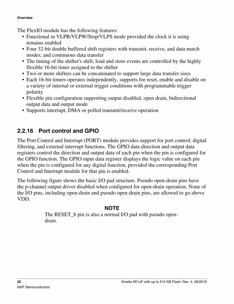
2.2.16 Port control and GPIO
The Port Control and Interrupt (PORT) module provides support for port control, digitalfiltering, and external interrupt functions. The GPIO data direction and output dataregisters control the direction and output data of each pin when the pin is configured forthe GPIO function. The GPIO input data register displays the logic value on each pinwhen the pin is configured for any digital function, provided the corresponding PortControl and Interrupt module for that pin is enabled.
The following figure shows the basic I/O pad structure. Pseudo open-drain pins havethe p-channel output driver disabled when configured for open-drain operation. None ofthe I/O pins, including open-drain and pseudo open-drain pins, are allowed to go aboveVDD.
NOTEThe RESET_b pin is also a normal I/O pad with pseudo open-drain.
Overview
22 Kinetis KE1xF with up to 512 KB Flash, Rev. 4, 06/2019
NXP Semiconductors
ESD Bus
VDD
PE
PS
RPULL
Digital output
Analog input
Digital input
MU
X
LPF
IIFE
IBE
IBE=1 whenever MUX≠000
DSE
Figure 5. I/O simplified block diagram
The PORT module has the following features:• all PIN support interrupt enable• Configurable edge (rising, falling, or both) or level sensitive interrupt type• Support DMA request• Asynchronous wake-up in low-power modes• Configurable pullup, pulldown, and pull-disable on select pins• Configurable high and low drive strength on selected pins• Configurable passive filter on selected pins• Individual mux control field supporting analog or pin disabled, GPIO, and up to
chip-specific digital functions• Pad configuration fields are functional in all digital pin muxing modes.
The GPIO module has the following features:• Port Data Input register visible in all digital pin-multiplexing modes• Port Data Output register with corresponding set/clear/toggle registers• Port Data Direction register• GPIO support single-cycle access via fast GPIO.
Overview
Kinetis KE1xF with up to 512 KB Flash, Rev. 4, 06/2019 23
NXP Semiconductors
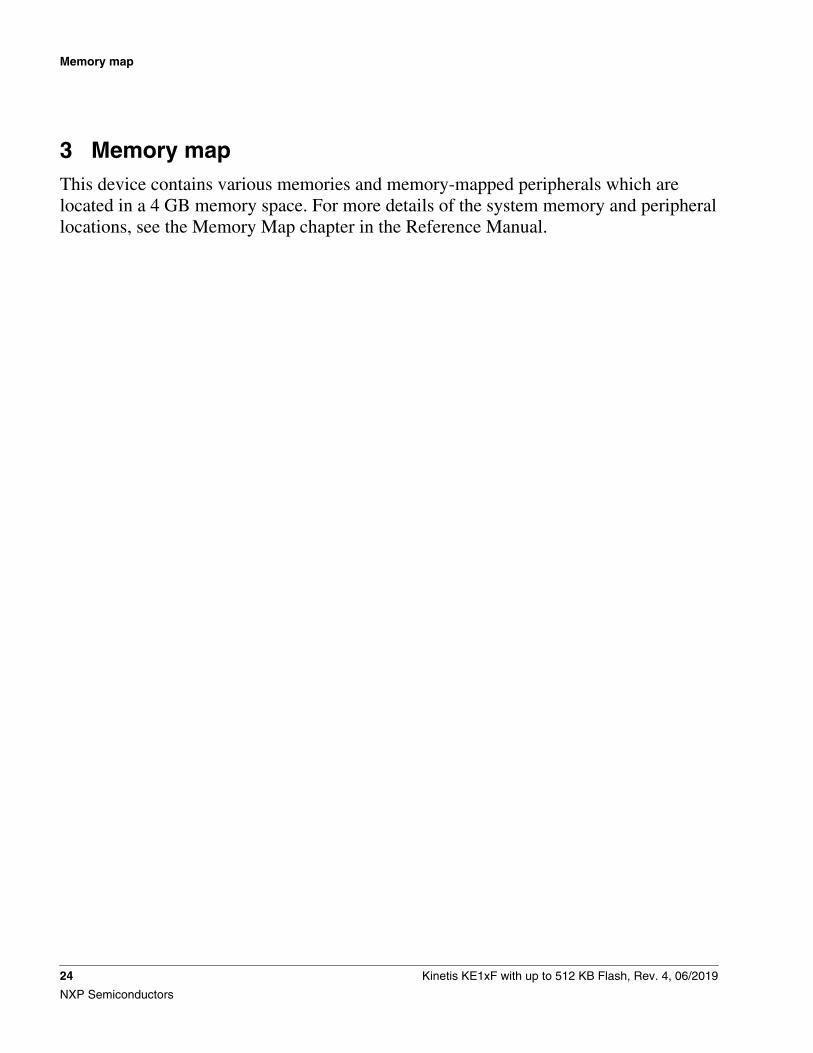
3 Memory mapThis device contains various memories and memory-mapped peripherals which arelocated in a 4 GB memory space. For more details of the system memory and peripherallocations, see the Memory Map chapter in the Reference Manual.
Memory map
24 Kinetis KE1xF with up to 512 KB Flash, Rev. 4, 06/2019
NXP Semiconductors
0x1C00_0000
0x1C00_3FFF
AIPS-Lite
0x1C00_3FFF0x1C00_4000
0x200F_FFFF
0x400F_F0000x400F_FFFF
0x1C00_0000
0xE000_0000
0xE000_E000
0xE000_F000
0xE00F_FFFF
0xE00F_F000
DMA TCD
GPIO controller (aliased to 400F_F000)
Reserved
4003_4000: FlexCAN0
Reserved
Flash memory unit
DMAMUX0
PDB0
LPSPI0
LPSPI1
CRC
Reserved
Reserved
Reserved
Reserved
4003_F000: DAC0
ADC2
LPIT0FTM0FTM1FTM2ADC0
RTC
LPTMR0
SIM
PORT APORT BPORT CPORT DPORT E
WDOG
SCG
TRGMUX0
PWT
FlexIO
EWM
PCC
OSC32
LPI2C0
LPI2C1Reserved
Reserved
Reserved
CMP0
PMC
SMCRCM
0x4000_80000x4000_9000
0x4000_D000
0x4000_F0000x4001_00000x4002_0000
0x4002_10000x4002_2000
0x4002_7000
0x4002_C0000x4002_D000
0x4002_8000
0x4002_E0000x4003_2000
0x4003_C0000x4003_B000
0x4003_A000
0x4003_90000x4003_80000x4003_7000
0x4003_3000
0x4003_E0000x4004_0000
0x4003_D000
0x4004_1000
0x4004_90000x4004_8000
0x4004_A000
0x4004_E000
0x4004_D0000x4004_C0000x4004_B000
0x4005_A0000x4005_7000
0x4005_6000
0x4005_30000x4005_2000
0x4005_B0000x4006_00000x4006_1000
0x4006_4000
0x4006_7000
0x4006_60000x4006_5000
0x4006_2000
0x4006_8000
0x4007_3000
0x4007_5000
0x4007_E000
0x4007_4000
0x4007_FFFF0x4007_F000
0x4007_D000
0x4000_1000
0x4000_0000
0x07FF_FFFF
0x0000_0000
0x4008_0000
eDMA
ADC1
0x4003_6000
0x4006_3000TRGMUX1
0x4006_A000
0x4006_B000
0x4006_C000
LPUART0LPUART1
LPUART20x4006_D000
CMP1
0x1FF0_0000
0x2000_0000
ROM
AIPS peripherals
GPIO
System control space
Reserved
CoreROM table
Flash *
SRAM_L
SRAM_U
Reserved
Reserved
Reserved
Reserved
ReservedMPU
0x4000_E000
0x4000_A000
4003_1000: PDB1
4003_3000: PDB2
Reserved
CMP20x4007_6000
0x0800_0000
0x1FF0_0000
0x2010_0000
0xE000_0000
0xFFFF_FFFF
0xE010_0000
0x1800_0000
0x0000_0000
0x1000_0000
0x1400_0000
0x4010_0000
0x4000_0000
0x4400_0000
0x4200_0000
0x2200_0000
0x2400_0000
0x1001_0000
0x1400_1000
Private peripheral
Code space
Reserved
FlexRAM
FlexNVM
Reserved
Boot ROM
Publicperipheral
Data Space
Aliased to SRAM_U bit-band region
Aliased to AIPSand GPIO
bit-band region
Reserved
Reserved
Reserved
Reserved
Reserved
Reserved
0x1C00_0000
0x4000_0000
0x4002_50000x4002_6000 FTM3
FlexCAN1
0x0007_FFFF Reserved
Reserved
Reserved
Note:The size of Flash and SRAM varies for devices with different part numbers.See "Ordering information" in DataSheet for details.
Figure 6. Memory map
Memory map
Kinetis KE1xF with up to 512 KB Flash, Rev. 4, 06/2019 25
NXP Semiconductors
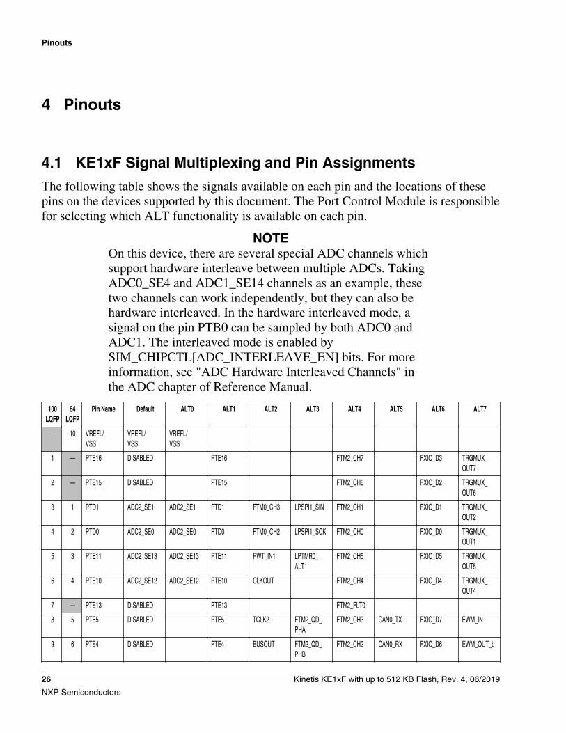
4 Pinouts
4.1 KE1xF Signal Multiplexing and Pin Assignments
The following table shows the signals available on each pin and the locations of thesepins on the devices supported by this document. The Port Control Module is responsiblefor selecting which ALT functionality is available on each pin.
NOTEOn this device, there are several special ADC channels whichsupport hardware interleave between multiple ADCs. TakingADC0_SE4 and ADC1_SE14 channels as an example, thesetwo channels can work independently, but they can also behardware interleaved. In the hardware interleaved mode, asignal on the pin PTB0 can be sampled by both ADC0 andADC1. The interleaved mode is enabled bySIM_CHIPCTL[ADC_INTERLEAVE_EN] bits. For moreinformation, see "ADC Hardware Interleaved Channels" inthe ADC chapter of Reference Manual.
100LQFP
64LQFP
Pin Name Default ALT0 ALT1 ALT2 ALT3 ALT4 ALT5 ALT6 ALT7
— 10 VREFL/VSS
VREFL/VSS
VREFL/VSS
1 — PTE16 DISABLED PTE16 FTM2_CH7 FXIO_D3 TRGMUX_OUT7
2 — PTE15 DISABLED PTE15 FTM2_CH6 FXIO_D2 TRGMUX_OUT6
3 1 PTD1 ADC2_SE1 ADC2_SE1 PTD1 FTM0_CH3 LPSPI1_SIN FTM2_CH1 FXIO_D1 TRGMUX_OUT2
4 2 PTD0 ADC2_SE0 ADC2_SE0 PTD0 FTM0_CH2 LPSPI1_SCK FTM2_CH0 FXIO_D0 TRGMUX_OUT1
5 3 PTE11 ADC2_SE13 ADC2_SE13 PTE11 PWT_IN1 LPTMR0_ALT1
FTM2_CH5 FXIO_D5 TRGMUX_OUT5
6 4 PTE10 ADC2_SE12 ADC2_SE12 PTE10 CLKOUT FTM2_CH4 FXIO_D4 TRGMUX_OUT4
7 — PTE13 DISABLED PTE13 FTM2_FLT0
8 5 PTE5 DISABLED PTE5 TCLK2 FTM2_QD_PHA
FTM2_CH3 CAN0_TX FXIO_D7 EWM_IN
9 6 PTE4 DISABLED PTE4 BUSOUT FTM2_QD_PHB
FTM2_CH2 CAN0_RX FXIO_D6 EWM_OUT_b
Pinouts
26 Kinetis KE1xF with up to 512 KB Flash, Rev. 4, 06/2019
NXP Semiconductors
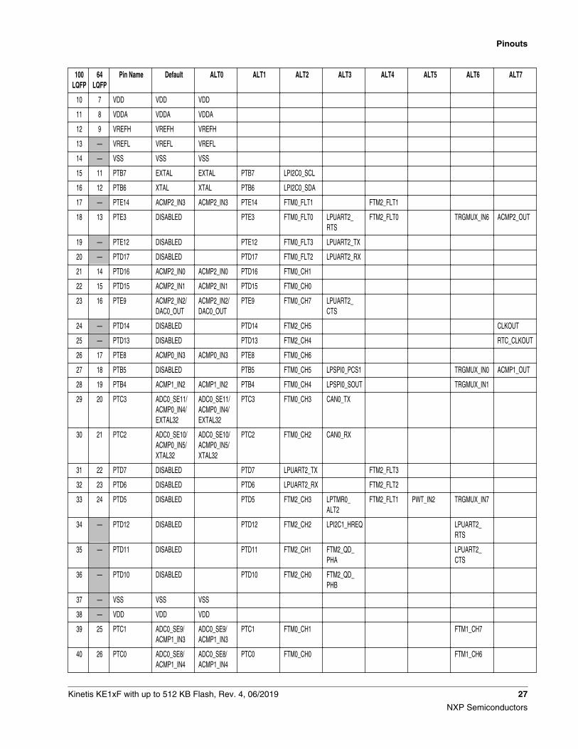
100LQFP
64LQFP
Pin Name Default ALT0 ALT1 ALT2 ALT3 ALT4 ALT5 ALT6 ALT7
10 7 VDD VDD VDD
11 8 VDDA VDDA VDDA
12 9 VREFH VREFH VREFH
13 — VREFL VREFL VREFL
14 — VSS VSS VSS
15 11 PTB7 EXTAL EXTAL PTB7 LPI2C0_SCL
16 12 PTB6 XTAL XTAL PTB6 LPI2C0_SDA
17 — PTE14 ACMP2_IN3 ACMP2_IN3 PTE14 FTM0_FLT1 FTM2_FLT1
18 13 PTE3 DISABLED PTE3 FTM0_FLT0 LPUART2_RTS
FTM2_FLT0 TRGMUX_IN6 ACMP2_OUT
19 — PTE12 DISABLED PTE12 FTM0_FLT3 LPUART2_TX
20 — PTD17 DISABLED PTD17 FTM0_FLT2 LPUART2_RX
21 14 PTD16 ACMP2_IN0 ACMP2_IN0 PTD16 FTM0_CH1
22 15 PTD15 ACMP2_IN1 ACMP2_IN1 PTD15 FTM0_CH0
23 16 PTE9 ACMP2_IN2/DAC0_OUT
ACMP2_IN2/DAC0_OUT
PTE9 FTM0_CH7 LPUART2_CTS
24 — PTD14 DISABLED PTD14 FTM2_CH5 CLKOUT
25 — PTD13 DISABLED PTD13 FTM2_CH4 RTC_CLKOUT
26 17 PTE8 ACMP0_IN3 ACMP0_IN3 PTE8 FTM0_CH6
27 18 PTB5 DISABLED PTB5 FTM0_CH5 LPSPI0_PCS1 TRGMUX_IN0 ACMP1_OUT
28 19 PTB4 ACMP1_IN2 ACMP1_IN2 PTB4 FTM0_CH4 LPSPI0_SOUT TRGMUX_IN1
29 20 PTC3 ADC0_SE11/ACMP0_IN4/EXTAL32
ADC0_SE11/ACMP0_IN4/EXTAL32
PTC3 FTM0_CH3 CAN0_TX
30 21 PTC2 ADC0_SE10/ACMP0_IN5/XTAL32
ADC0_SE10/ACMP0_IN5/XTAL32
PTC2 FTM0_CH2 CAN0_RX
31 22 PTD7 DISABLED PTD7 LPUART2_TX FTM2_FLT3
32 23 PTD6 DISABLED PTD6 LPUART2_RX FTM2_FLT2
33 24 PTD5 DISABLED PTD5 FTM2_CH3 LPTMR0_ALT2
FTM2_FLT1 PWT_IN2 TRGMUX_IN7
34 — PTD12 DISABLED PTD12 FTM2_CH2 LPI2C1_HREQ LPUART2_RTS
35 — PTD11 DISABLED PTD11 FTM2_CH1 FTM2_QD_PHA
LPUART2_CTS
36 — PTD10 DISABLED PTD10 FTM2_CH0 FTM2_QD_PHB
37 — VSS VSS VSS
38 — VDD VDD VDD
39 25 PTC1 ADC0_SE9/ACMP1_IN3
ADC0_SE9/ACMP1_IN3
PTC1 FTM0_CH1 FTM1_CH7
40 26 PTC0 ADC0_SE8/ACMP1_IN4
ADC0_SE8/ACMP1_IN4
PTC0 FTM0_CH0 FTM1_CH6
Pinouts
Kinetis KE1xF with up to 512 KB Flash, Rev. 4, 06/2019 27
NXP Semiconductors
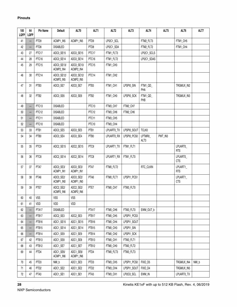
100LQFP
64LQFP
Pin Name Default ALT0 ALT1 ALT2 ALT3 ALT4 ALT5 ALT6 ALT7
41 — PTD9 ACMP1_IN5 ACMP1_IN5 PTD9 LPI2C1_SCL FTM2_FLT3 FTM1_CH5
42 — PTD8 DISABLED PTD8 LPI2C1_SDA FTM2_FLT2 FTM1_CH4
43 27 PTC17 ADC0_SE15 ADC0_SE15 PTC17 FTM1_FLT3 LPI2C1_SCLS
44 28 PTC16 ADC0_SE14 ADC0_SE14 PTC16 FTM1_FLT2 LPI2C1_SDAS
45 29 PTC15 ADC0_SE13/ACMP2_IN4
ADC0_SE13/ACMP2_IN4
PTC15 FTM1_CH3
46 30 PTC14 ADC0_SE12/ACMP2_IN5
ADC0_SE12/ACMP2_IN5
PTC14 FTM1_CH2
47 31 PTB3 ADC0_SE7 ADC0_SE7 PTB3 FTM1_CH1 LPSPI0_SIN FTM1_QD_PHA
TRGMUX_IN2
48 32 PTB2 ADC0_SE6 ADC0_SE6 PTB2 FTM1_CH0 LPSPI0_SCK FTM1_QD_PHB
TRGMUX_IN3
49 — PTC13 DISABLED PTC13 FTM3_CH7 FTM2_CH7
50 — PTC12 DISABLED PTC12 FTM3_CH6 FTM2_CH6
51 — PTC11 DISABLED PTC11 FTM3_CH5
52 — PTC10 DISABLED PTC10 FTM3_CH4
53 33 PTB1 ADC0_SE5 ADC0_SE5 PTB1 LPUART0_TX LPSPI0_SOUT TCLK0
54 34 PTB0 ADC0_SE4 ADC0_SE4 PTB0 LPUART0_RX LPSPI0_PCS0 LPTMR0_ALT3
PWT_IN3
55 35 PTC9 ADC2_SE15 ADC2_SE15 PTC9 LPUART1_TX FTM1_FLT1 LPUART0_RTS
56 36 PTC8 ADC2_SE14 ADC2_SE14 PTC8 LPUART1_RX FTM1_FLT0 LPUART0_CTS
57 37 PTA7 ADC0_SE3/ACMP1_IN1
ADC0_SE3/ACMP1_IN1
PTA7 FTM0_FLT2 RTC_CLKIN LPUART1_RTS
58 38 PTA6 ADC0_SE2/ACMP1_IN0
ADC0_SE2/ACMP1_IN0
PTA6 FTM0_FLT1 LPSPI1_PCS1 LPUART1_CTS
59 39 PTE7 ADC2_SE2/ACMP2_IN6
ADC2_SE2/ACMP2_IN6
PTE7 FTM0_CH7 FTM3_FLT0
60 40 VSS VSS VSS
61 41 VDD VDD VDD
62 — PTA17 DISABLED PTA17 FTM0_CH6 FTM3_FLT0 EWM_OUT_b
63 — PTB17 ADC2_SE3 ADC2_SE3 PTB17 FTM0_CH5 LPSPI1_PCS3
64 — PTB16 ADC1_SE15 ADC1_SE15 PTB16 FTM0_CH4 LPSPI1_SOUT
65 — PTB15 ADC1_SE14 ADC1_SE14 PTB15 FTM0_CH3 LPSPI1_SIN
66 — PTB14 ADC1_SE9 ADC1_SE9 PTB14 FTM0_CH2 LPSPI1_SCK
67 42 PTB13 ADC1_SE8 ADC1_SE8 PTB13 FTM0_CH1 FTM3_FLT1
68 43 PTB12 ADC1_SE7 ADC1_SE7 PTB12 FTM0_CH0 FTM3_FLT2
69 44 PTD4 ADC1_SE6/ACMP1_IN6
ADC1_SE6/ACMP1_IN6
PTD4 FTM0_FLT3 FTM3_FLT3
70 45 PTD3 NMI_b ADC1_SE3 PTD3 FTM3_CH5 LPSPI1_PCS0 FXIO_D5 TRGMUX_IN4 NMI_b
71 46 PTD2 ADC1_SE2 ADC1_SE2 PTD2 FTM3_CH4 LPSPI1_SOUT FXIO_D4 TRGMUX_IN5
72 47 PTA3 ADC1_SE1 ADC1_SE1 PTA3 FTM3_CH1 LPI2C0_SCL EWM_IN LPUART0_TX
Pinouts
28 Kinetis KE1xF with up to 512 KB Flash, Rev. 4, 06/2019
NXP Semiconductors
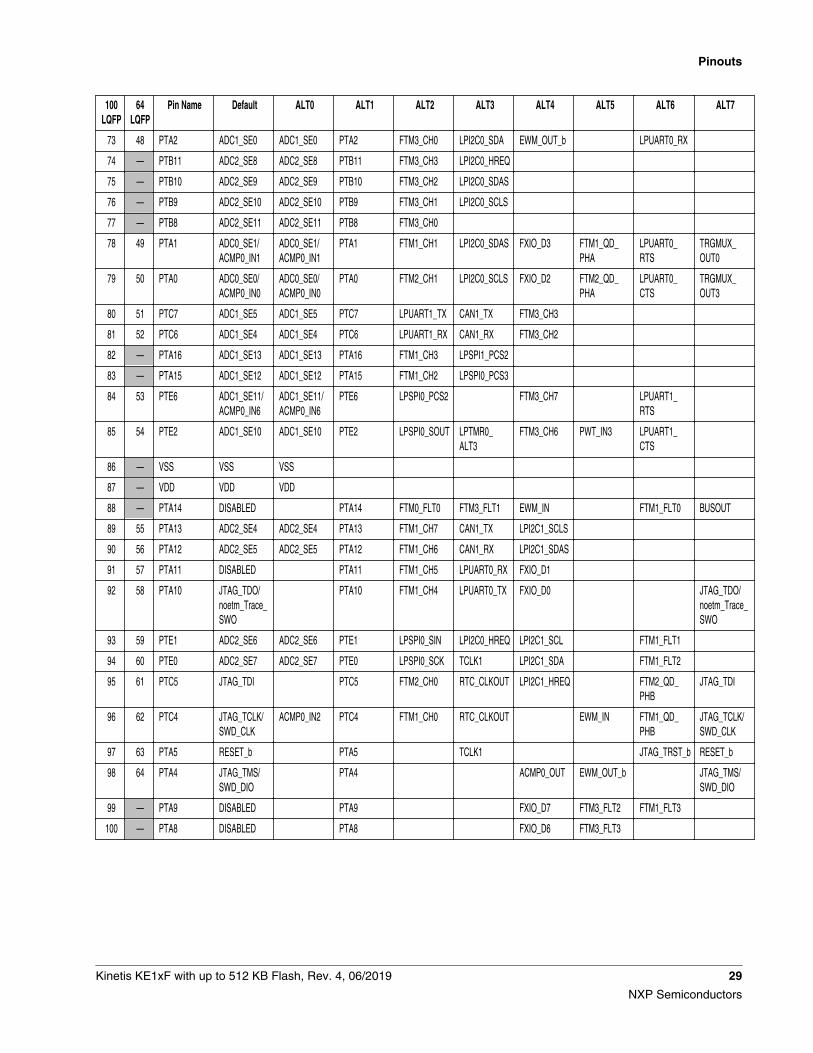
100LQFP
64LQFP
Pin Name Default ALT0 ALT1 ALT2 ALT3 ALT4 ALT5 ALT6 ALT7
73 48 PTA2 ADC1_SE0 ADC1_SE0 PTA2 FTM3_CH0 LPI2C0_SDA EWM_OUT_b LPUART0_RX
74 — PTB11 ADC2_SE8 ADC2_SE8 PTB11 FTM3_CH3 LPI2C0_HREQ
75 — PTB10 ADC2_SE9 ADC2_SE9 PTB10 FTM3_CH2 LPI2C0_SDAS
76 — PTB9 ADC2_SE10 ADC2_SE10 PTB9 FTM3_CH1 LPI2C0_SCLS
77 — PTB8 ADC2_SE11 ADC2_SE11 PTB8 FTM3_CH0
78 49 PTA1 ADC0_SE1/ACMP0_IN1
ADC0_SE1/ACMP0_IN1
PTA1 FTM1_CH1 LPI2C0_SDAS FXIO_D3 FTM1_QD_PHA
LPUART0_RTS
TRGMUX_OUT0
79 50 PTA0 ADC0_SE0/ACMP0_IN0
ADC0_SE0/ACMP0_IN0
PTA0 FTM2_CH1 LPI2C0_SCLS FXIO_D2 FTM2_QD_PHA
LPUART0_CTS
TRGMUX_OUT3
80 51 PTC7 ADC1_SE5 ADC1_SE5 PTC7 LPUART1_TX CAN1_TX FTM3_CH3
81 52 PTC6 ADC1_SE4 ADC1_SE4 PTC6 LPUART1_RX CAN1_RX FTM3_CH2
82 — PTA16 ADC1_SE13 ADC1_SE13 PTA16 FTM1_CH3 LPSPI1_PCS2
83 — PTA15 ADC1_SE12 ADC1_SE12 PTA15 FTM1_CH2 LPSPI0_PCS3
84 53 PTE6 ADC1_SE11/ACMP0_IN6
ADC1_SE11/ACMP0_IN6
PTE6 LPSPI0_PCS2 FTM3_CH7 LPUART1_RTS
85 54 PTE2 ADC1_SE10 ADC1_SE10 PTE2 LPSPI0_SOUT LPTMR0_ALT3
FTM3_CH6 PWT_IN3 LPUART1_CTS
86 — VSS VSS VSS
87 — VDD VDD VDD
88 — PTA14 DISABLED PTA14 FTM0_FLT0 FTM3_FLT1 EWM_IN FTM1_FLT0 BUSOUT
89 55 PTA13 ADC2_SE4 ADC2_SE4 PTA13 FTM1_CH7 CAN1_TX LPI2C1_SCLS
90 56 PTA12 ADC2_SE5 ADC2_SE5 PTA12 FTM1_CH6 CAN1_RX LPI2C1_SDAS
91 57 PTA11 DISABLED PTA11 FTM1_CH5 LPUART0_RX FXIO_D1
92 58 PTA10 JTAG_TDO/noetm_Trace_SWO
PTA10 FTM1_CH4 LPUART0_TX FXIO_D0 JTAG_TDO/noetm_Trace_SWO
93 59 PTE1 ADC2_SE6 ADC2_SE6 PTE1 LPSPI0_SIN LPI2C0_HREQ LPI2C1_SCL FTM1_FLT1
94 60 PTE0 ADC2_SE7 ADC2_SE7 PTE0 LPSPI0_SCK TCLK1 LPI2C1_SDA FTM1_FLT2
95 61 PTC5 JTAG_TDI PTC5 FTM2_CH0 RTC_CLKOUT LPI2C1_HREQ FTM2_QD_PHB
JTAG_TDI
96 62 PTC4 JTAG_TCLK/SWD_CLK
ACMP0_IN2 PTC4 FTM1_CH0 RTC_CLKOUT EWM_IN FTM1_QD_PHB
JTAG_TCLK/SWD_CLK
97 63 PTA5 RESET_b PTA5 TCLK1 JTAG_TRST_b RESET_b
98 64 PTA4 JTAG_TMS/SWD_DIO
PTA4 ACMP0_OUT EWM_OUT_b JTAG_TMS/SWD_DIO
99 — PTA9 DISABLED PTA9 FXIO_D7 FTM3_FLT2 FTM1_FLT3
100 — PTA8 DISABLED PTA8 FXIO_D6 FTM3_FLT3
Pinouts
Kinetis KE1xF with up to 512 KB Flash, Rev. 4, 06/2019 29
NXP Semiconductors
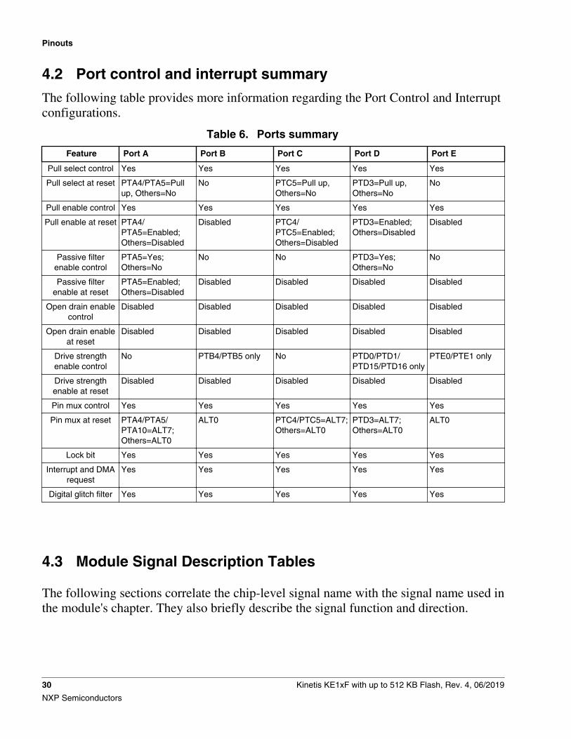
4.2 Port control and interrupt summary
The following table provides more information regarding the Port Control and Interruptconfigurations.
Table 6. Ports summary
Feature Port A Port B Port C Port D Port E
Pull select control Yes Yes Yes Yes Yes
Pull select at reset PTA4/PTA5=Pullup, Others=No
No PTC5=Pull up,Others=No
PTD3=Pull up,Others=No
No
Pull enable control Yes Yes Yes Yes Yes
Pull enable at reset PTA4/PTA5=Enabled;Others=Disabled
Disabled PTC4/PTC5=Enabled;Others=Disabled
PTD3=Enabled;Others=Disabled
Disabled
Passive filterenable control
PTA5=Yes;Others=No
No No PTD3=Yes;Others=No
No
Passive filterenable at reset
PTA5=Enabled;Others=Disabled
Disabled Disabled Disabled Disabled
Open drain enablecontrol
Disabled Disabled Disabled Disabled Disabled
Open drain enableat reset
Disabled Disabled Disabled Disabled Disabled
Drive strengthenable control
No PTB4/PTB5 only No PTD0/PTD1/PTD15/PTD16 only
PTE0/PTE1 only
Drive strengthenable at reset
Disabled Disabled Disabled Disabled Disabled
Pin mux control Yes Yes Yes Yes Yes
Pin mux at reset PTA4/PTA5/PTA10=ALT7;Others=ALT0
ALT0 PTC4/PTC5=ALT7;Others=ALT0
PTD3=ALT7;Others=ALT0
ALT0
Lock bit Yes Yes Yes Yes Yes
Interrupt and DMArequest
Yes Yes Yes Yes Yes
Digital glitch filter Yes Yes Yes Yes Yes
4.3 Module Signal Description Tables
The following sections correlate the chip-level signal name with the signal name used inthe module's chapter. They also briefly describe the signal function and direction.
Pinouts
30 Kinetis KE1xF with up to 512 KB Flash, Rev. 4, 06/2019
NXP Semiconductors
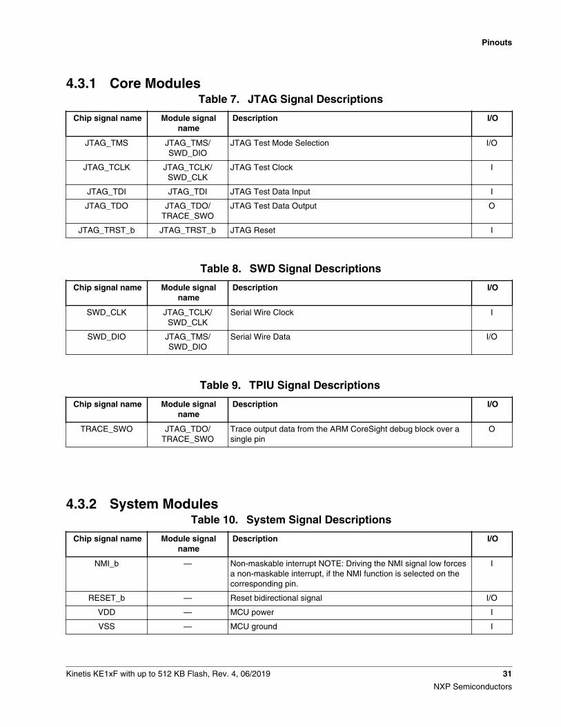
4.3.1 Core ModulesTable 7. JTAG Signal Descriptions
Chip signal name Module signalname
Description I/O
JTAG_TMS JTAG_TMS/SWD_DIO
JTAG Test Mode Selection I/O
JTAG_TCLK JTAG_TCLK/SWD_CLK
JTAG Test Clock I
JTAG_TDI JTAG_TDI JTAG Test Data Input I
JTAG_TDO JTAG_TDO/TRACE_SWO
JTAG Test Data Output O
JTAG_TRST_b JTAG_TRST_b JTAG Reset I
Table 8. SWD Signal Descriptions
Chip signal name Module signalname
Description I/O
SWD_CLK JTAG_TCLK/SWD_CLK
Serial Wire Clock I
SWD_DIO JTAG_TMS/SWD_DIO
Serial Wire Data I/O
Table 9. TPIU Signal Descriptions
Chip signal name Module signalname
Description I/O
TRACE_SWO JTAG_TDO/TRACE_SWO
Trace output data from the ARM CoreSight debug block over asingle pin
O
4.3.2 System ModulesTable 10. System Signal Descriptions
Chip signal name Module signalname
Description I/O
NMI_b — Non-maskable interrupt NOTE: Driving the NMI signal low forcesa non-maskable interrupt, if the NMI function is selected on thecorresponding pin.
I
RESET_b — Reset bidirectional signal I/O
VDD — MCU power I
VSS — MCU ground I
Pinouts
Kinetis KE1xF with up to 512 KB Flash, Rev. 4, 06/2019 31
NXP Semiconductors
Table 11. EWM Signal Descriptions
Chip signal name Module signalname
Description I/O
EWM_IN EWM_in EWM input for safety status of external safety circuits. The polarityof EWM_IN is programmable using the EWM_CTRL[ASSIN] bit.The default polarity is active-low.
I
EWM_OUT_b EWM_out EWM reset out signal O
4.3.3 Clock ModulesTable 12. OSC (in SCG) Signal Descriptions
Chipsignalname
Module signal name Description I/O
EXTAL EXTAL External clock/Oscillator input I
XTAL XTAL Oscillator output O
Table 13. RTC Oscillator (OSC32) Signal Descriptions
Chip signal name Module signalname
Description I/O
EXTAL32 EXTAL32 32.768 kHz oscillator input I
XTAL32 XTAL32 32.768 kHz oscillator output O
4.3.4 AnalogTable 14. ADCn Signal Descriptions
Chip signal name Module signalname
Description I/O
ADCn_SE[15:0] AD[15:0] Single-Ended Analog Channel Inputs I
VREFH VREFSH Voltage Reference Select High I
VREFL VREFSL Voltage Reference Select Low I
VDDA VDDA Analog Power Supply I
Table 15. DAC0 Signal Descriptions
Chip signal name Module signalname
Description I/O
DAC0_OUT — DAC output O
Pinouts
32 Kinetis KE1xF with up to 512 KB Flash, Rev. 4, 06/2019
NXP Semiconductors
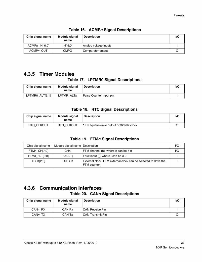
Table 16. ACMPn Signal Descriptions
Chip signal name Module signalname
Description I/O
ACMPn_IN[ 6:0] IN[ 6:0] Analog voltage inputs I
ACMPn_OUT CMPO Comparator output O
4.3.5 Timer ModulesTable 17. LPTMR0 Signal Descriptions
Chip signal name Module signalname
Description I/O
LPTMR0_ALT[3:1] LPTMR_ALTn Pulse Counter Input pin I
Table 18. RTC Signal Descriptions
Chip signal name Module signalname
Description I/O
RTC_CLKOUT RTC_CLKOUT 1 Hz square-wave output or 32 kHz clock O
Table 19. FTMn Signal Descriptions
Chip signal name Module signal name Description I/O
FTMn_CH[7:0] CHn FTM channel (n), where n can be 7-0 I/O
FTMn_FLT[3:0] FAULTj Fault input (j), where j can be 3-0 I
TCLK[2:0] EXTCLK External clock. FTM external clock can be selected to drive theFTM counter.
I
4.3.6 Communication InterfacesTable 20. CANn Signal Descriptions
Chip signal name Module signalname
Description I/O
CANn_RX CAN Rx CAN Receive Pin I
CANn_TX CAN Tx CAN Transmit Pin O
Pinouts
Kinetis KE1xF with up to 512 KB Flash, Rev. 4, 06/2019 33
NXP Semiconductors
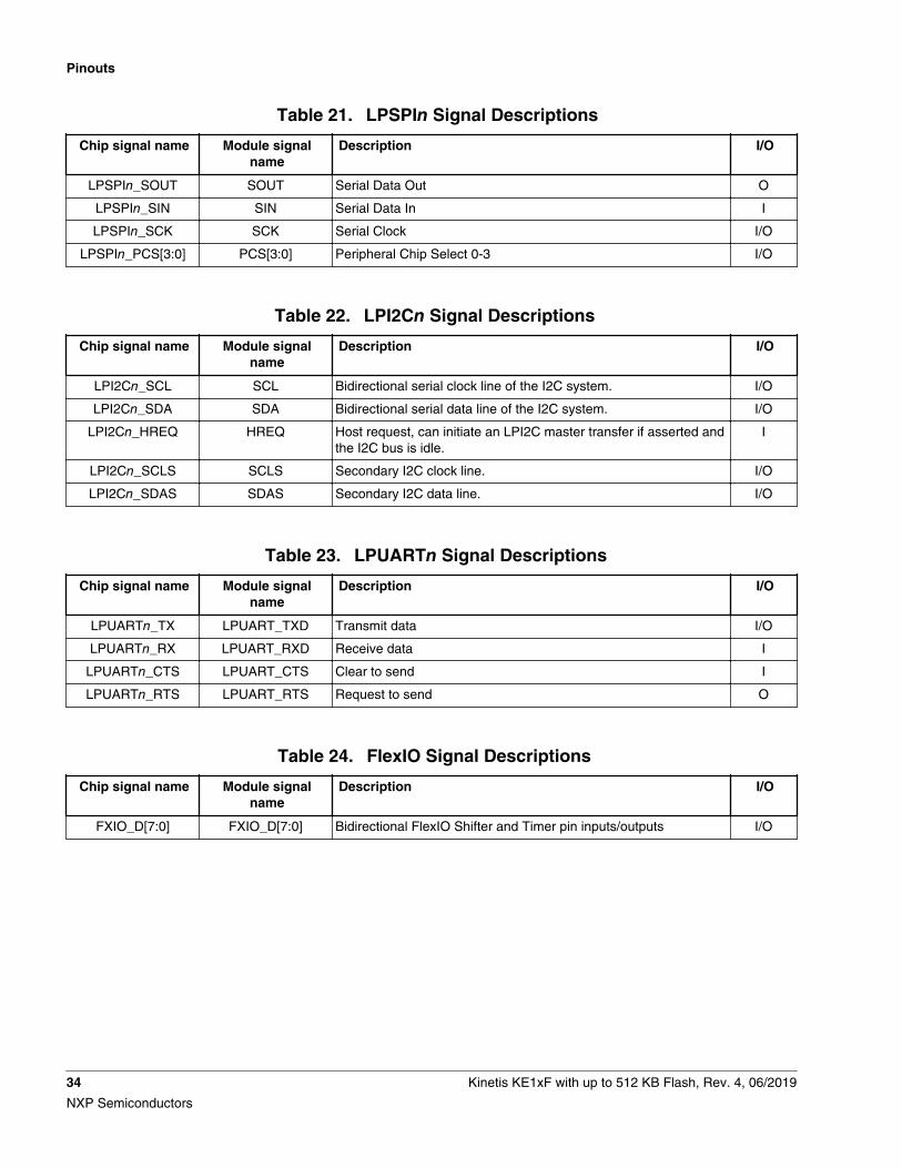
Table 21. LPSPIn Signal Descriptions
Chip signal name Module signalname
Description I/O
LPSPIn_SOUT SOUT Serial Data Out O
LPSPIn_SIN SIN Serial Data In I
LPSPIn_SCK SCK Serial Clock I/O
LPSPIn_PCS[3:0] PCS[3:0] Peripheral Chip Select 0-3 I/O
Table 22. LPI2Cn Signal Descriptions
Chip signal name Module signalname
Description I/O
LPI2Cn_SCL SCL Bidirectional serial clock line of the I2C system. I/O
LPI2Cn_SDA SDA Bidirectional serial data line of the I2C system. I/O
LPI2Cn_HREQ HREQ Host request, can initiate an LPI2C master transfer if asserted andthe I2C bus is idle.
I
LPI2Cn_SCLS SCLS Secondary I2C clock line. I/O
LPI2Cn_SDAS SDAS Secondary I2C data line. I/O
Table 23. LPUARTn Signal Descriptions
Chip signal name Module signalname
Description I/O
LPUARTn_TX LPUART_TXD Transmit data I/O
LPUARTn_RX LPUART_RXD Receive data I
LPUARTn_CTS LPUART_CTS Clear to send I
LPUARTn_RTS LPUART_RTS Request to send O
Table 24. FlexIO Signal Descriptions
Chip signal name Module signalname
Description I/O
FXIO_D[7:0] FXIO_D[7:0] Bidirectional FlexIO Shifter and Timer pin inputs/outputs I/O
Pinouts
34 Kinetis KE1xF with up to 512 KB Flash, Rev. 4, 06/2019
NXP Semiconductors
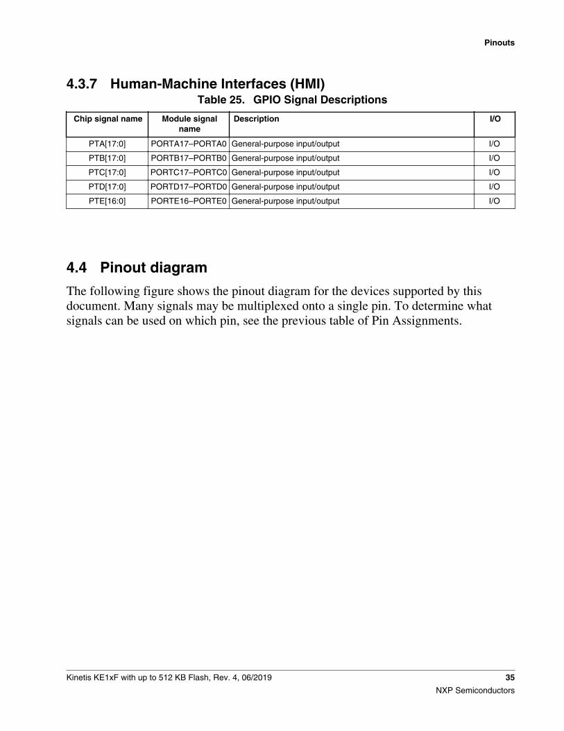
4.3.7 Human-Machine Interfaces (HMI)Table 25. GPIO Signal Descriptions
Chip signal name Module signalname
Description I/O
PTA[17:0] PORTA17–PORTA0 General-purpose input/output I/O
PTB[17:0] PORTB17–PORTB0 General-purpose input/output I/O
PTC[17:0] PORTC17–PORTC0 General-purpose input/output I/O
PTD[17:0] PORTD17–PORTD0 General-purpose input/output I/O
PTE[16:0] PORTE16–PORTE0 General-purpose input/output I/O
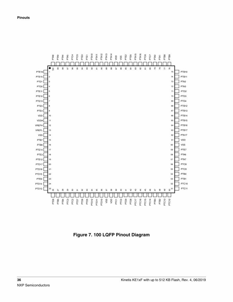
4.4 Pinout diagram
The following figure shows the pinout diagram for the devices supported by thisdocument. Many signals may be multiplexed onto a single pin. To determine whatsignals can be used on which pin, see the previous table of Pin Assignments.
Pinouts
Kinetis KE1xF with up to 512 KB Flash, Rev. 4, 06/2019 35
NXP Semiconductors
60
59
58
57
56
55
54
53
52
51
20
19
18
17
16
15
14
13
12
11
10
9
8
7
6
5
4
3
2
1
PTD17
PTE12
PTE3
PTE14
PTB6
PTB7
VSS
VREFL
VREFH
VDDA
VDD
PTE4
PTE5
PTE13
PTE10
PTE11
PTD0
PTD1
PTE15
PTE16 75
74
73
72
71
70
69
68
67
66
65
64
63
62
61
PTB10
PTB11
PTA2
PTA3
PTD2
PTD3
PTD4
PTB12
PTB13
PTB14
PTB15
PTB16
PTB17
PTA17
VDD
VSS
PTE7
PTA6
PTA7
PTC8
PTC9
PTB0
PTB1
PTC10
PTC1125
24
23
22
21
PTD13
PTD14
PTE9
PTD15
PTD16
403938373635343332313029282726
99 79 78 77 76
PTA
9
PTA
0
PTA
1
PT
B8
PT
B9
50494847464544434241
PT
C12
PT
C13
PT
B2
PT
B3
PT
C14
PT
C15
PT
C16
PT
C17
PT
D8
PT
D9
PT
C0
PT
C1
VD
D
VS
S
PT
D10
PT
D11
PT
D12
PT
D5
PT
D6
PT
D7
PT
C2
PT
C3
PT
B4
PT
B5
PT
E8
98P
TA4
97P
TA5
96P
TC
4
95P
TC
5
94P
TE
0
93P
TE
1
92P
TA10
91P
TA11
90P
TA12
89P
TA13
88P
TA14
80P
TC
7
PT
C6
PTA
16
818283P
TA15
84P
TE
6
85P
TE
2
86V
SS
87V
DD
100
PTA
8
Figure 7. 100 LQFP Pinout Diagram
Pinouts
36 Kinetis KE1xF with up to 512 KB Flash, Rev. 4, 06/2019
NXP Semiconductors
PT
C3
PT
B4
PT
B5
PT
E8
PTE9
PTD15
PTD16
PTE3
PTB6
PTB7
VREFL / VSS
VREFH
VDDA
VDD
PTE4
PTE5
PTE10
PTE11
PTD0
PTD1
60 59 58 57 56 55 54 53 52 51 50 49
48
47
46
45
44
43
42
41
40
39
38
37
36
35
34
33
32313029282726252423222120191817
16
15
14
13
12
11
10
9
8
7
6
5
4
3
2
1
64 63 62 61
PTA
4
PTA
5
PT
C4
PT
C5
PT
E0
PT
E1
PTA
10
PTA
11
PTA
12
PTA
13
PT
E2
PT
E6
PT
C6
PT
C7
PTA
0
PTA
1
PTA2
PTA3
PTD2
PTD3
PTD4
PTB12
PTB13
VDD
VSS
PTE7
PTA6
PTA7
PTC8
PTC9
PTB0
PTB1
PT
B2
PT
B3
PT
C14
PT
C15
PT
C16
PT
C17
PT
C0
PT
C1
PT
D5
PT
D6
PT
D7
PT
C2
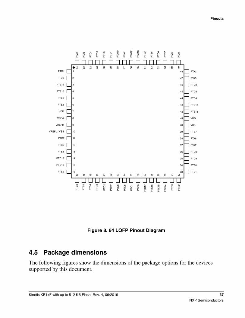
Figure 8. 64 LQFP Pinout Diagram
4.5 Package dimensions
The following figures show the dimensions of the package options for the devicessupported by this document.
Pinouts
Kinetis KE1xF with up to 512 KB Flash, Rev. 4, 06/2019 37
NXP Semiconductors
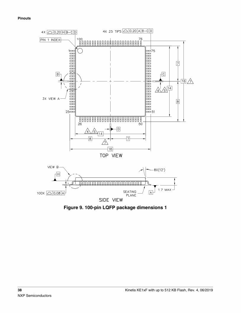
Figure 9. 100-pin LQFP package dimensions 1
Pinouts
38 Kinetis KE1xF with up to 512 KB Flash, Rev. 4, 06/2019
NXP Semiconductors
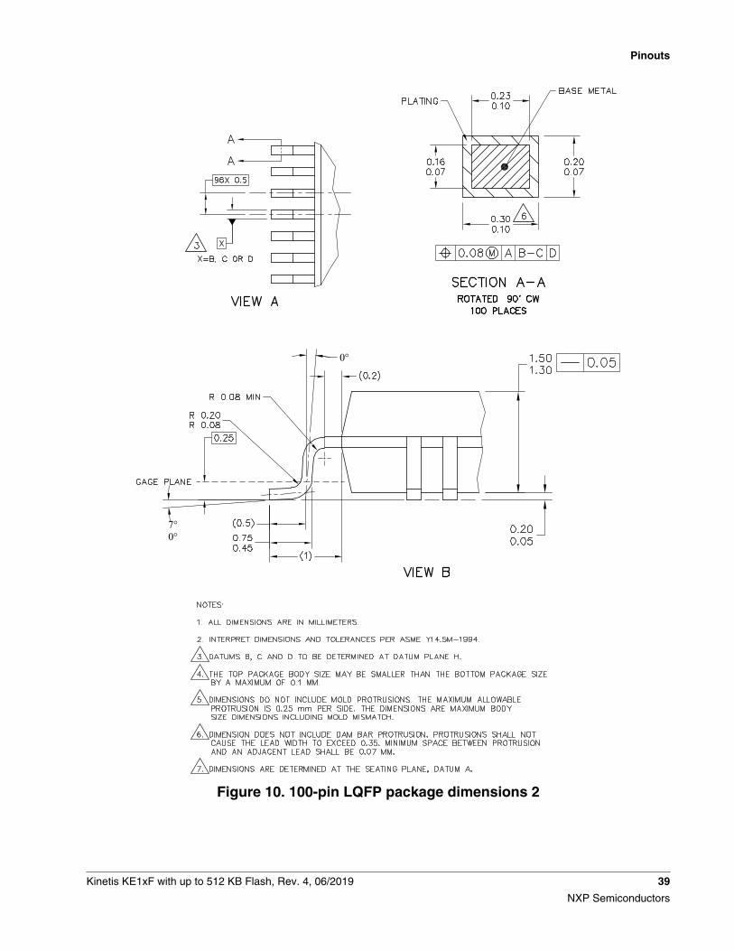
Figure 10. 100-pin LQFP package dimensions 2
Pinouts
Kinetis KE1xF with up to 512 KB Flash, Rev. 4, 06/2019 39
NXP Semiconductors
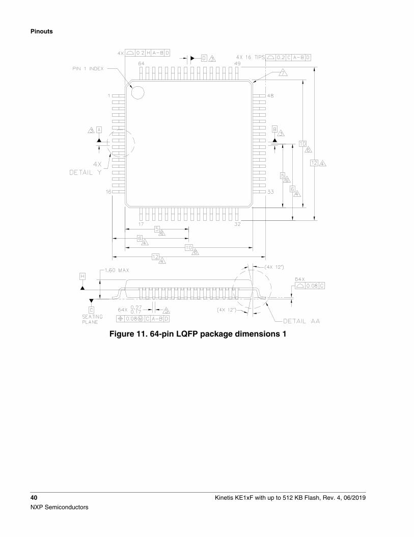
Figure 11. 64-pin LQFP package dimensions 1
Pinouts
40 Kinetis KE1xF with up to 512 KB Flash, Rev. 4, 06/2019
NXP Semiconductors
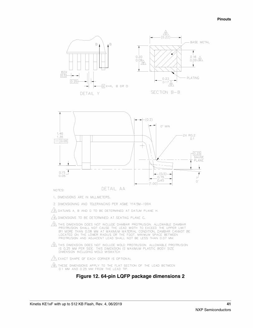
Figure 12. 64-pin LQFP package dimensions 2
Pinouts
Kinetis KE1xF with up to 512 KB Flash, Rev. 4, 06/2019 41
NXP Semiconductors
5 Electrical characteristics
5.1 Terminology and guidelines
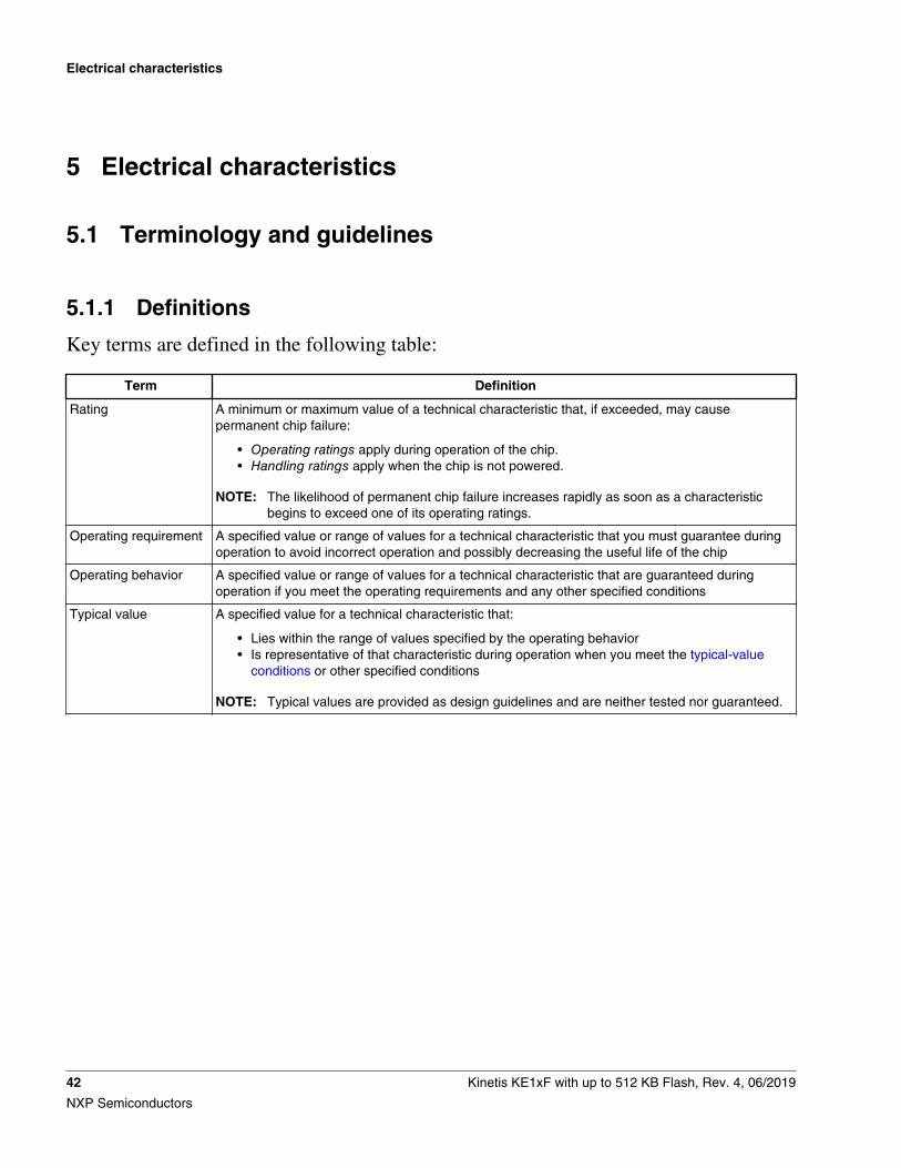
5.1.1 Definitions
Key terms are defined in the following table:
Term Definition
Rating A minimum or maximum value of a technical characteristic that, if exceeded, may causepermanent chip failure:
• Operating ratings apply during operation of the chip.• Handling ratings apply when the chip is not powered.
NOTE: The likelihood of permanent chip failure increases rapidly as soon as a characteristicbegins to exceed one of its operating ratings.
Operating requirement A specified value or range of values for a technical characteristic that you must guarantee duringoperation to avoid incorrect operation and possibly decreasing the useful life of the chip
Operating behavior A specified value or range of values for a technical characteristic that are guaranteed duringoperation if you meet the operating requirements and any other specified conditions
Typical value A specified value for a technical characteristic that:
• Lies within the range of values specified by the operating behavior• Is representative of that characteristic during operation when you meet the typical-value
conditions or other specified conditions
NOTE: Typical values are provided as design guidelines and are neither tested nor guaranteed.
Electrical characteristics
42 Kinetis KE1xF with up to 512 KB Flash, Rev. 4, 06/2019
NXP Semiconductors
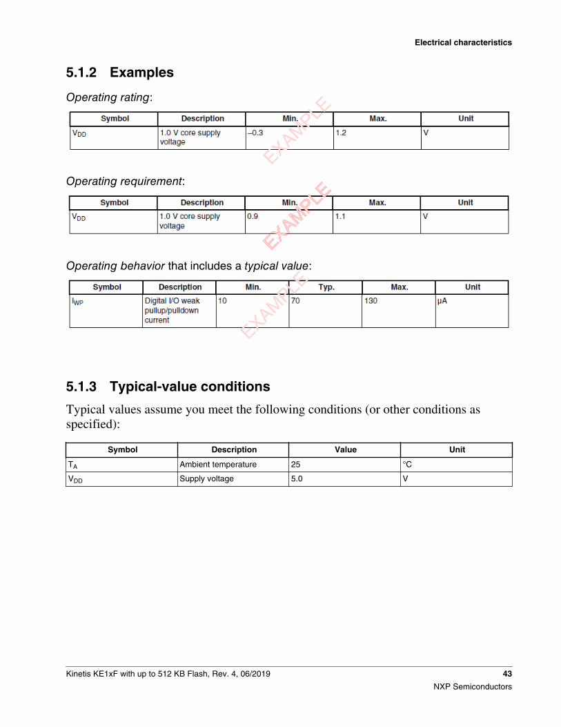
5.1.2 Examples
Operating rating:
Operating requirement:
Operating behavior that includes a typical value:
EXAMPLE
EXAMPLE
EXAMPLE
EXAMPLE
5.1.3 Typical-value conditions
Typical values assume you meet the following conditions (or other conditions asspecified):
Symbol Description Value Unit
TA Ambient temperature 25 °C
VDD Supply voltage 5.0 V
Electrical characteristics
Kinetis KE1xF with up to 512 KB Flash, Rev. 4, 06/2019 43
NXP Semiconductors
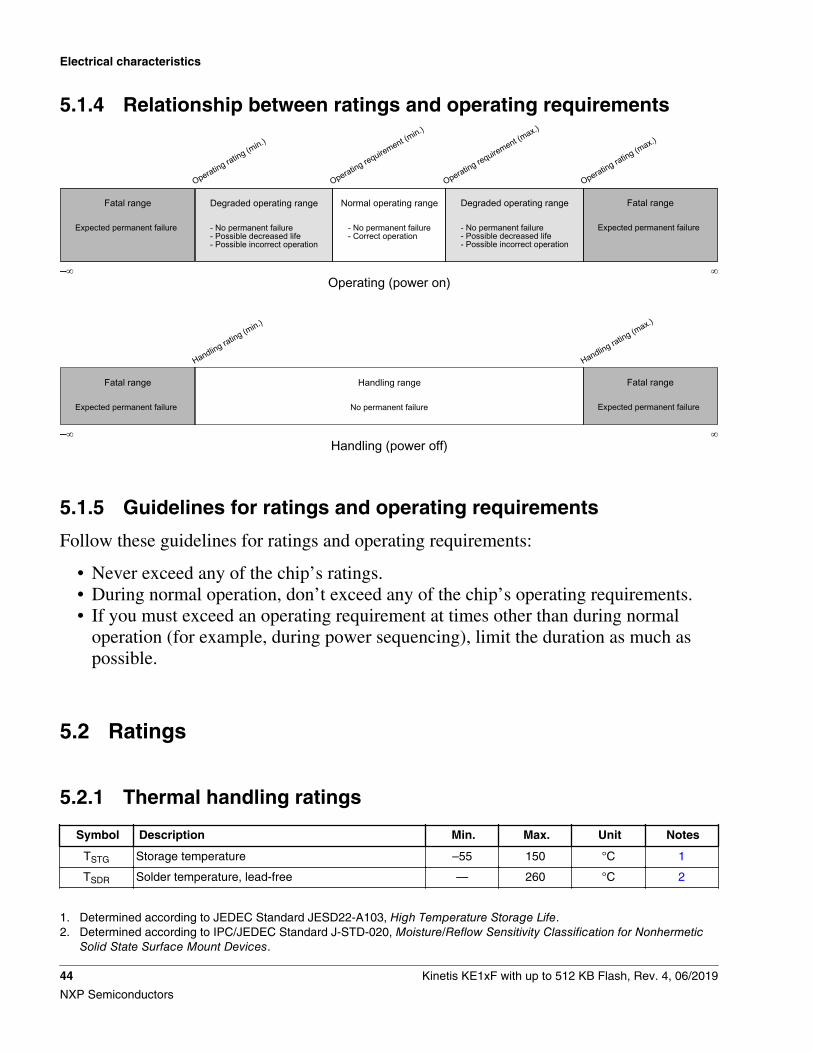
5.1.4 Relationship between ratings and operating requirements
–∞
- No permanent failure- Correct operation
Normal operating rangeFatal range
Expected permanent failure
Fatal range
Expected permanent failure
∞
Operating rating (max.)
Operating requirement (max.)
Operating requirement (min.)
Operating rating (min.)
Operating (power on)
Degraded operating range Degraded operating range
–∞
No permanent failure
Handling rangeFatal range
Expected permanent failure
Fatal range
Expected permanent failure
∞
Handling rating (max.)
Handling rating (min.)
Handling (power off)
- No permanent failure- Possible decreased life- Possible incorrect operation
- No permanent failure- Possible decreased life- Possible incorrect operation
5.1.5 Guidelines for ratings and operating requirements
Follow these guidelines for ratings and operating requirements:
• Never exceed any of the chip’s ratings.• During normal operation, don’t exceed any of the chip’s operating requirements.• If you must exceed an operating requirement at times other than during normal
operation (for example, during power sequencing), limit the duration as much aspossible.
5.2 Ratings
5.2.1 Thermal handling ratings
Symbol Description Min. Max. Unit Notes
TSTG Storage temperature –55 150 °C 1
TSDR Solder temperature, lead-free — 260 °C 2
1. Determined according to JEDEC Standard JESD22-A103, High Temperature Storage Life.2. Determined according to IPC/JEDEC Standard J-STD-020, Moisture/Reflow Sensitivity Classification for Nonhermetic
Solid State Surface Mount Devices.
Electrical characteristics
44 Kinetis KE1xF with up to 512 KB Flash, Rev. 4, 06/2019
NXP Semiconductors
5.2.2 Moisture handling ratings
Symbol Description Min. Max. Unit Notes
MSL Moisture sensitivity level — 3 — 1
1. Determined according to IPC/JEDEC Standard J-STD-020, Moisture/Reflow Sensitivity Classification for NonhermeticSolid State Surface Mount Devices.
5.2.3 ESD handling ratings
Symbol Description Min. Max. Unit Notes
VHBM Electrostatic discharge voltage, human body model − 6000 6000 V 1
VCDM Electrostatic discharge voltage, charged-devicemodel
2
All pins except the corner pins − 500 500 V
Corner pins only − 750 750 V
ILAT Latch-up current at ambient temperature upper limit − 100 100 mA 3
1. Determined according to JEDEC Standard JESD22-A114, Electrostatic Discharge (ESD) Sensitivity Testing HumanBody Model (HBM).
2. Determined according to JEDEC Standard JESD22-C101, Field-Induced Charged-Device Model Test Method forElectrostatic-Discharge-Withstand Thresholds of Microelectronic Components.
3. Determined according to JEDEC Standard JESD78, IC Latch-Up Test.
5.2.4 Voltage and current operating ratings
NOTEFunctional operating conditions appear in the "DC electricalspecifications". Absolute maximum ratings are stress ratingsonly, and functional operation at the maximum values is notguaranteed. Stress beyond the listed maximum values mayaffect device reliability or cause permanent damage to thedevice.
Table 26. Voltage and current operating ratings
Symbol Description Min. Max. Unit
VDD Supply voltage –0.3 5.8 1 V
IDD Digital supply current — 80 mA
Table continues on the next page...
Electrical characteristics
Kinetis KE1xF with up to 512 KB Flash, Rev. 4, 06/2019 45
NXP Semiconductors
Table 26. Voltage and current operating ratings (continued)
Symbol Description Min. Max. Unit
VIO IO pin input voltage VSS – 0.3 VDD + 0.3 V
ID Instantaneous maximum current single pin limit (applies toall port pins)
–25 25 mA
VDDA Analog supply voltage VDD – 0.1 VDD + 0.1 V
1. 60s lifetime - No restrictions, i.e. the part can switch.
10 hours lifetime - Device in reset, i.e. the part cannot switch.
5.3 General
5.3.1 Nonswitching electrical specifications
5.3.1.1 Voltage and current operating requirementsTable 27. Voltage and current operating requirements
Symbol Description Min. Max. Unit Notes
VDD Supply voltage 2.7 5.5 V
VDDA Analog supply voltage 2.7 5.5 V
VDD –VDDA
VDD-to-VDDA differential voltage – 0.1 0.1 V
VSS –VSSA
VSS-to-VSSA differential voltage – 0.1 0.1 V
IICIO DC injection current — single pin
VIN < VSS - 0.3 V (Negative current injection) − 3 — mA 1
VIN > VDD + 0.3 V (Positive current injection) — + 3 mA
IICcont Contiguous pin DC injection current —regional limit, includes sum of negativeinjection currents or sum of positive injectioncurrents of 16 contiguous pins
− 25 + 25 mA
VODPU Open drain pullup voltage level VDD VDD V 2
1. All pins are internally clamped to VSS and VDD through ESD protection diodes. If VIN is less than VSS – 0.3V or greaterthan VDD + 0.3V, a current limiting resistor is required. The negative DC injection current limiting resistor is calculated asR=(VSS – 0.3V–VIN)/|IICIO|. The positive injection current limiting resistor is calculated as R=[VIN–(VDD + 0.3V)]/|IICIO|.The actual resistor values should be an order of magnitude higher to tolerate transient voltages.
2. Open drain outputs must be pulled to VDD.
Electrical characteristics
46 Kinetis KE1xF with up to 512 KB Flash, Rev. 4, 06/2019
NXP Semiconductors
5.3.1.2 DC electrical specifications at 3.3 V Range and 5.0 V RangeTable 28. DC electrical specifications
Symbol Parameter Value Unit Notes
Min Typ Max
VDD I/O Supply Voltage 1
@ VDD = 3.3 V
2.7 3.3 4 V
@ VDD = 5.0 V 4 — 5.5 V
Vih Input Buffer High Voltage
@ VDD = 3.3 V
0.7 × VDD — VDD + 0.3 V
@ VDD = 5.0 V 0.65 × VDD — VDD + 0.3 V
Vil Input Buffer Low Voltage
@ VDD = 3.3 V
VSS − 0.3 — 0.3 × VDD V
@ VDD = 5.0 V VSS − 0.3 — 0.35 ×VDD
V
Vhys Input Buffer Hysteresis 0.06 × VDD — — V
Ioh_5 Normal drive I/O current source capabilitymeasured when pad = (VDD − 0.8 V)
@ VDD = 3.3 V
2.8 — — mA
@ VDD = 5.0 V 4.8 — — mA
Iol_5 Normal drive I/O current sink capabilitymeasured when pad = 0.8 V
@ VDD = 3.3 V
2.4 — — mA
@ VDD = 5.0 V 4.4 — — mA
Ioh_20 High drive I/O current source capabilitymeasured when pad = (VDD − 0.8 V), 2
@ VDD = 3.3 V
10.8 — — mA
@ VDD = 5.0 V 18.5 — — mA 3
Iol_20 High drive I/O current sink capability measuredwhen pad = 0.8 V4
@ VDD = 3.3 V
10.1 — — mA
@ VDD = 5.0 V 18.5 — — mA 3
I_leak Hi-Z (Off state) leakage current (per pin) — — 300 nA 5, 6
VOH Output high voltage 7
Normal drive pad (2.7 V ≤ VDD ≤ 4.0 V, IOH = −2.8 mA)
VDD – 0.8 — — V
Normal drive pad (4.0 V ≤ VDD ≤ 5.5 V, IOH = −4.8 mA)
VDD – 0.8 — — V
High drive pad (2.7 V ≤ VDD ≤ 4.0 V, IOH = −10.8 mA)
VDD – 0.8 — — V
High drive pad (4.0 V ≤ VDD ≤ 5.5 V, IOH = −18.5 mA)
VDD – 0.8 — — V
IOHT Output high current total for all ports — — 100 mA
Table continues on the next page...
Electrical characteristics
Kinetis KE1xF with up to 512 KB Flash, Rev. 4, 06/2019 47
NXP Semiconductors
Table 28. DC electrical specifications (continued)
Symbol Parameter Value Unit Notes
Min Typ Max
VOL Output low voltage 7
Normal drive pad (2.7 V ≤ VDD ≤ 4.0 V, IOH = −2.8 mA)
— — 0.8 V
Normal drive pad (4.0 V ≤ VDD ≤ 5.5 V, IOH = −4.8 mA)
— — 0.8 V
High drive pad (2.7 V ≤ VDD ≤ 4.0 V, IOH = −10.8 mA)
— — 0.8 V
High drive pad (4.0 V ≤ VDD ≤ 5.5 V, IOH = −18.5 mA)
— — 0.8 V
IOLT Output low current total for all ports — — 100 mA
IIN Input leakage current (per pin) for full temperature range
@ VDD = 3.3 V
8, 7
All pins other than high drive port pins — 0.002 0.5 μA
High drive port pins — 0.004 0.5 μA
Input leakage current (per pin) for full temperature range
@ VDD = 5.5 V
All pins other than high drive port pins — 0.005 0.5 μA
High drive port pins — 0.010 0.5 μA
RPU Internal pull-up resistors
@ VDD = 3.3 V
20 — 65 kΩ 9
@ VDD = 5.0 V 20 — 50 kΩ
RPD Internal pull-down resistors
@ VDD = 3.3 V
20 — 65 kΩ 10
@ VDD = 5.0 V 20 — 50 kΩ
1. Max power supply ramp rate is 500 V/ms.2. The value given is measured at high drive strength mode. For value at low drive strength mode see the Ioh_5 value
given above.3. The 20 mA I/O pin is capable of switching a 50 pF load at up to 40 MHz.4. The value given is measured at high drive strength mode. For value at low drive strength mode see the Iol_5 value given
above.5. Refers to the current that leaks into the core when the pad is in Hi-Z (Off state).6. Maximum pin leakage current at the ambient temperature upper limit.7. PTD0, PTD1, PTD15, PTD16, PTB4, PTB5, PTE0 and PTE1 I/O have both high drive and normal drive capability
selected by the associated Portx_PCRn[DSE] control bit. All other GPIOs are normal drive only.8. Refers to the pin leakage on the GPIOs when they are OFF.9. Measured at VDD supply voltage = VDD min and input V = VSS10. Measured at VDD supply voltage = VDD min and input V = VDD
Electrical characteristics
48 Kinetis KE1xF with up to 512 KB Flash, Rev. 4, 06/2019
NXP Semiconductors
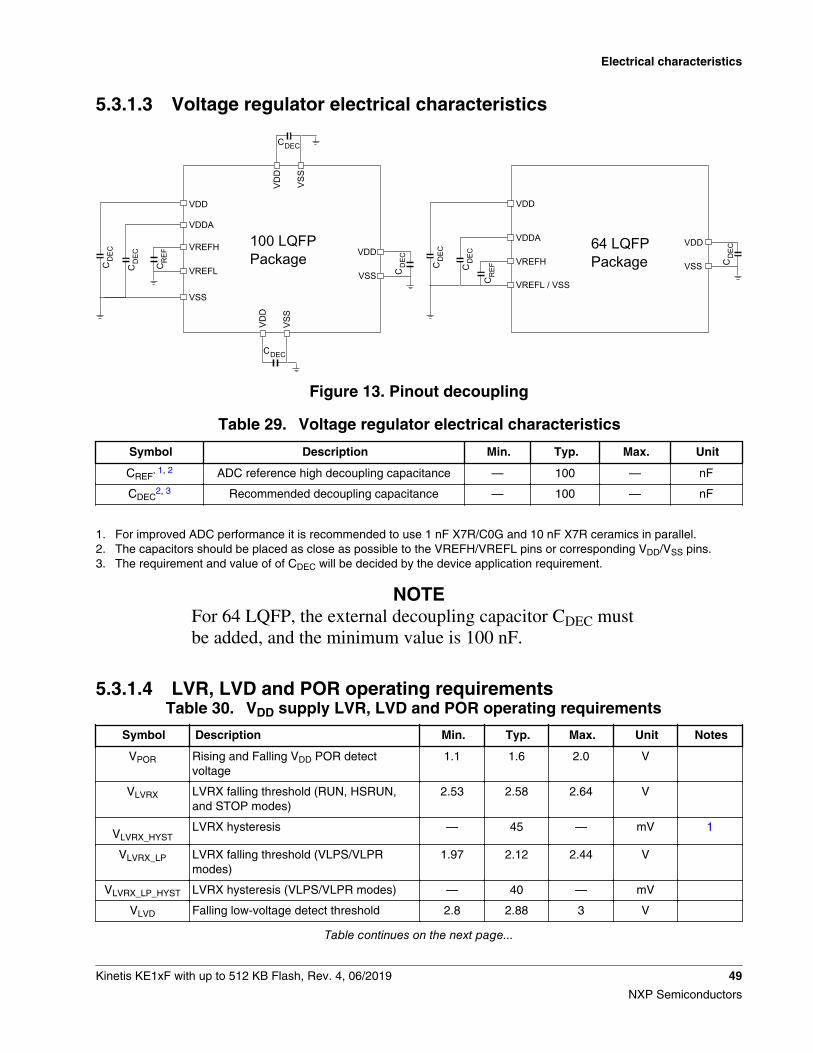
5.3.1.3 Voltage regulator electrical characteristics
VDD
VDDA
VREFH
VREFL
VSS
VDD
VSS
VDD
VSSVD
D
VSS
100 LQFP Package
VDD
VSS
VDDA
VREFH
VREFL / VSS
64 LQFP PackageC
DEC
C REF
C REFC
DEC
CDEC
CDEC
CD
EC CD
EC
CD
EC
CD
EC
VDD
Figure 13. Pinout decoupling
Table 29. Voltage regulator electrical characteristics
Symbol Description Min. Typ. Max. Unit
CREF, 1, 2 ADC reference high decoupling capacitance — 100 — nF
CDEC2, 3 Recommended decoupling capacitance — 100 — nF
1. For improved ADC performance it is recommended to use 1 nF X7R/C0G and 10 nF X7R ceramics in parallel.2. The capacitors should be placed as close as possible to the VREFH/VREFL pins or corresponding VDD/VSS pins.3. The requirement and value of of CDEC will be decided by the device application requirement.
NOTEFor 64 LQFP, the external decoupling capacitor CDEC mustbe added, and the minimum value is 100 nF.
5.3.1.4 LVR, LVD and POR operating requirementsTable 30. VDD supply LVR, LVD and POR operating requirements
Symbol Description Min. Typ. Max. Unit Notes
VPOR Rising and Falling VDD POR detectvoltage
1.1 1.6 2.0 V
VLVRX LVRX falling threshold (RUN, HSRUN,and STOP modes)
2.53 2.58 2.64 V
VLVRX_HYSTLVRX hysteresis — 45 — mV 1
VLVRX_LP LVRX falling threshold (VLPS/VLPRmodes)
1.97 2.12 2.44 V
VLVRX_LP_HYST LVRX hysteresis (VLPS/VLPR modes) — 40 — mV
VLVD Falling low-voltage detect threshold 2.8 2.88 3 V
Table continues on the next page...
Electrical characteristics
Kinetis KE1xF with up to 512 KB Flash, Rev. 4, 06/2019 49
NXP Semiconductors
Table 30. VDD supply LVR, LVD and POR operating requirements (continued)
Symbol Description Min. Typ. Max. Unit Notes
VLVD_HYSTLVD hysteresis — 50 — mV 1
VLVW Falling low-voltage warning threshold 4.19 4.31 4.5 V
VLVW_HYST LVW hysteresis 68 mV 1
VBG Bandgap voltage reference 0.97 1.00 1.03 V
1. Rising threshold is the sum of falling threshold and hysteresis voltage.
5.3.1.5 Power mode transition operating behaviorsTable 31. Power mode transition operating behaviors
Description System Clock Core, Bus, Flashfrequency (MHz)
Min. Typ. (μs)1 Max. (μs)2
STOP→RUN FIRC 48, 48, 24 — 7.32 12.8
STOP→RUN SPLL 120, 60, 24 — 7.04 12.6
VLPS→RUN FIRC 48, 48, 24 — 7.32 12.9
VLPS→RUN SPLL 120, 60, 24 — 142 149
RUN→HSRUN SPLL 120, 60, 24→120, 60, 24 — 3.96 6.74
HSRUN→RUN SPLL 120, 60, 24→120, 60, 24 — 0.704 1.155
RUN→VLPR SPLL→SIRC 120, 60, 24→4, 4, 1 — 7.62 8.54
VLPR→RUN SIRC→FIRC 4, 4, 1→48, 48, 24 — 19.4 31.8
VLPR→RUN SIRC→SPLL 4, 4, 1→120, 60, 24 — 157 168
WAIT→RUN FIRC 48, 48, 24 — 0.476 0.554
WAIT→RUN SPLL 120, 60, 24 — 0.260 0.310
VLPW→VLPR SIRC 4, 4, 1 — 10.3 16.2
VLPS→VLPR SIRC 4, 4, 1 — 10.8 15.7
VLPW→RUN FIRC (reset value) 48, 48, 24 (reset value) — 128 143
tPOR3 FIRC (reset value) 48, 48, 24 (reset value) — 112 122
1. Typical value is the average of values tested at Temperature=25 and VDD=3.3 V.2. Max value is mean+6×sigma of tested values at the worst case of ambient temperature range and VDD 2.7 V to 5.5 V.3. After a POR event, the amount of time from the point VDD reaches the reference voltage 2.7 V to execution of the first
instruction, across the operating temperature range of the chip.
5.3.1.6 Power consumptionThe following table shows the power consumption targets for the device in variousmodes of operations.
Electrical characteristics
50 Kinetis KE1xF with up to 512 KB Flash, Rev. 4, 06/2019
NXP Semiconductors
NOTEThe maximum values stated in the following table representcharacterized results equivalent to the mean plus three timesthe standard deviation (mean + 3 sigma).
Table 32. Power consumption operating behaviors
Mode Symbol ClockConfigur
ation
Description Temperature
Min Typ Max1 Units
HSRUN IDD_HSRUN PLL Running CoreMark in Flash in ComputeOperation mode.
Core@168MHz, bus @84MHz,flash@24MHz VDD=5V
25 — 44.50 46.36 mA
105 — 51.88 59.46
PLL Running CoreMark in Flash allperipheral clock disabled.
Core@168MHz, bus @84MHz,flash@24MHz VDD=5V
25 — 50.49 52.35
105 — 58.31 65.89
PLL Running CoreMark in Flash, allperipheral clock enabled.
Core@168MHz, bus @84MHz,flash@24MHz VDD=5V
25 — 60.51 62.37
105 — 68.62 76.20
PLL Running While(1) loop in Flash, allperipheral clock disabled.
Core@168MHz, bus @84MHz,flash@24MHz VDD=5V
25 — 52.74 54.60
105 — 60.76 68.34
PLL Running While(1) loop in Flash allperipheral clock enabled.
Core@168MHz, bus @84MHz,flash@24MHz VDD=5V
25 — 62.48 64.34
105 — 70.75 78.33
RUN IDD_RUN PLL Running CoreMark in Flash in ComputeOperation mode.
Core@120MHz, bus @60MHz,flash@24MHz VDD=5V
25 — 29.04 29.67 mA
105 — 34.82 40.43
PLL Running CoreMark in Flash allperipheral clock disabled.
Core@120MHz, bus @60MHz,flash@24MHz VDD=5V
25 — 33.29 33.92
105 — 39.08 44.69
PLL Running CoreMark in Flash, allperipheral clock enabled.
Core@120MHz, bus @60MHz,flash@24MHz VDD=5V
25 — 41.00 41.63
105 — 47.00 52.61
PLL Running While(1) loop in Flash, allperipheral clock disabled.
Core@120MHz, bus @60MHz,flash@24MHz VDD=5V
25 — 34.59 35.22
105 — 40.68 46.29
Table continues on the next page...
Electrical characteristics
Kinetis KE1xF with up to 512 KB Flash, Rev. 4, 06/2019 51
NXP Semiconductors
Table 32. Power consumption operating behaviors (continued)
Mode Symbol ClockConfigur
ation
Description Temperature
Min Typ Max1 Units
PLL Running While(1) loop in Flash allperipheral clock enabled.
Core@120MHz, bus @60MHz,flash@24MHz VDD=5V
25 — 39.87 40.50
105 — 46.03 51.64
IRC48M Running CoreMark in Flash in ComputeOperation mode.
Core@48MHz, bus @48MHz, flash@24MHz , VDD=5V
25 — 14.02 14.65
105 — 19.76 25.37
IRC48M Running CoreMark in Flash allperipheral clock disabled.
Core@48MHz, bus @48MHz, flash@24MHz , VDD=5V
25 — 16.83 17.46
105 — 22.64 28.25
IRC48M Running CoreMark in Flash, allperipheral clock enabled.
Core@48MHz, bus @48MHz, flash@24MHz , VDD=5V
25 — 19.70 20.33
105 — 25.59 31.20
IRC48M Running While(1) loop in Flash, allperipheral clock disabled.
Core@48MHz, bus @48MHz, flash@24MHz , VDD=5V
25 — 17.22 17.85
105 — 23.23 28.84
VLPR IDD_VLPR IRC8M Very Low Power Run Core Mark inFlash in Compute Operation mode.
Core@4MHz, bus @4MHz, flash@1MHz, VDD=5V
25 — 1.52 1.63 mA
IRC8M Very Low Power Run Core Mark inFlash all peripheral clock disabled.
Core@4MHz, bus @4MHz, flash@1MHz, VDD=5V
25 — 1.73 1.84
IRC8M Very Low Power Run Core Mark inFlash all peripheral clock enabled.
Core@4MHz, bus @4MHz, flash@1MHz, VDD=5V
25 — 1.95 2.06
IRC8M Very Low Power Run While(1) loop inFlash all peripheral clock disabled.
Core@4MHz, bus @4MHz, flash@1MHz, VDD=5V
25 — 1.77 1.88
IRC8M Very Low Power Run While(1) loop inFlash all peripheral clock enabled.
Core@4MHz, bus @4MHz, flash@1MHz, VDD=5V
25 — 1.96 2.07
IRC2M Very Low Power Run While(1) loop inFlash all peripheral clock disabled.
25 — 1.19 1.30
Table continues on the next page...
Electrical characteristics
52 Kinetis KE1xF with up to 512 KB Flash, Rev. 4, 06/2019
NXP Semiconductors
Table 32. Power consumption operating behaviors (continued)
Mode Symbol ClockConfigur
ation
Description Temperature
Min Typ Max1 Units
Core@2MHz, bus @2MHz, flash@1MHz, VDD=5V
IRC2M Very Low Power Run While(1) loop inFlash all peripheral clock enabled.
Core@2MHz, bus @2MHz, flash@1MHz, VDD=5V
25 — 1.28 1.39
WAIT IDD_WAIT PLL core disabled, system@120MHz, bus@60MHz, flash disabled (flash dozeenabled), VDD=5 V, all peripheralclocks disabled
25 — 14.13 14.78 mA
IRC48M core disabled, system@48 MHz, bus@48MHz, flash disabled (flash dozeenabled), VDD=5 V, all peripheralclocks disabled
25 — 8.50 9.15
VLPW IDD_VLPW IRC8M Very Low Power Wait current, coredisabled system@4MHz, bus@4Mhzand flash@1MHz, all peripheral clocksdisabled, VDD=5V
25 — 1.08 1.18 mA
IRC2M Very Low Power Wait current, coredisabled system@2MHz, bus@2Mhzand flash@1MHz, all peripheral clocksdisabled, VDD=5V
25 — 0.84 0.94
STOP IDD_STOP - Stop mode current, VDD=5V, clock biasenabled 2
25 andbelow
— 175 484 μA
50 — 438 1014
85 — 1433 2864
105 — 2860 5263
STOP IDD_STOP - Stop mode current, VDD=5V, clock biasdisabled 2
25 andbelow
— 92 299 μA
50 — 211 530
85 — 671 1397
105 — 1287 2502
VLPS IDD_VLPS - Very Low Power Stop current, VDD=5V,clock bias enabled 2
25 andbelow
— 175 483 μA
50 — 424 998
85 — 1367 2792
105 — 2864 5258
VLPS IDD_VLPS - Very Low Power Stop current, VDD=5V,clock bias disabled 2
25 andbelow
— 91 298 μA
50 — 208 525
85 — 656 1378
105 — 1305 2514
Electrical characteristics
Kinetis KE1xF with up to 512 KB Flash, Rev. 4, 06/2019 53
NXP Semiconductors
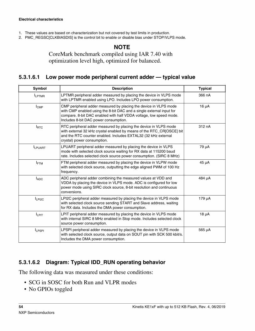
1. These values are based on characterization but not covered by test limits in production.2. PMC_REGSC[CLKBIASDIS] is the control bit to enable or disable bias under STOP/VLPS mode.
NOTECoreMark benchmark compiled using IAR 7.40 withoptimization level high, optimized for balanced.
5.3.1.6.1 Low power mode peripheral current adder — typical value
Symbol Description Typical
ILPTMR LPTMR peripheral adder measured by placing the device in VLPS modewith LPTMR enabled using LPO. Includes LPO power consumption.
366 nA
ICMP CMP peripheral adder measured by placing the device in VLPS modewith CMP enabled using the 8-bit DAC and a single external input forcompare. 8-bit DAC enabled with half VDDA voltage, low speed mode.Includes 8-bit DAC power consumption.
16 μA
IRTC RTC peripheral adder measured by placing the device in VLPS modewith external 32 kHz crystal enabled by means of the RTC_CR[OSCE] bitand the RTC counter enabled. Includes EXTAL32 (32 kHz externalcrystal) power consumption.
312 nA
ILPUART LPUART peripheral adder measured by placing the device in VLPSmode with selected clock source waiting for RX data at 115200 baudrate. Includes selected clock source power consumption. (SIRC 8 MHz)
79 μA
IFTM FTM peripheral adder measured by placing the device in VLPW modewith selected clock source, outputting the edge aligned PWM of 100 Hzfrequency.
45 μA
IADC ADC peripheral adder combining the measured values at VDD andVDDA by placing the device in VLPS mode. ADC is configured for lowpower mode using SIRC clock source, 8-bit resolution and continuousconversions.
484 μA
ILPI2C LPI2C peripheral adder measured by placing the device in VLPS modewith selected clock source sending START and Slave address, waitingfor RX data. Includes the DMA power consumption.
179 μA
ILPIT LPIT peripheral adder measured by placing the device in VLPS modewith internal SIRC 8 MHz enabled in Stop mode. Includes selected clocksource power consumption.
18 μA
ILPSPI LPSPI peripheral adder measured by placing the device in VLPS modewith selected clock source, output data on SOUT pin with SCK 500 kbit/s.Includes the DMA power consumption.
565 μA
5.3.1.6.2 Diagram: Typical IDD_RUN operating behavior
The following data was measured under these conditions:
• SCG in SOSC for both Run and VLPR modes• No GPIOs toggled
Electrical characteristics
54 Kinetis KE1xF with up to 512 KB Flash, Rev. 4, 06/2019
NXP Semiconductors
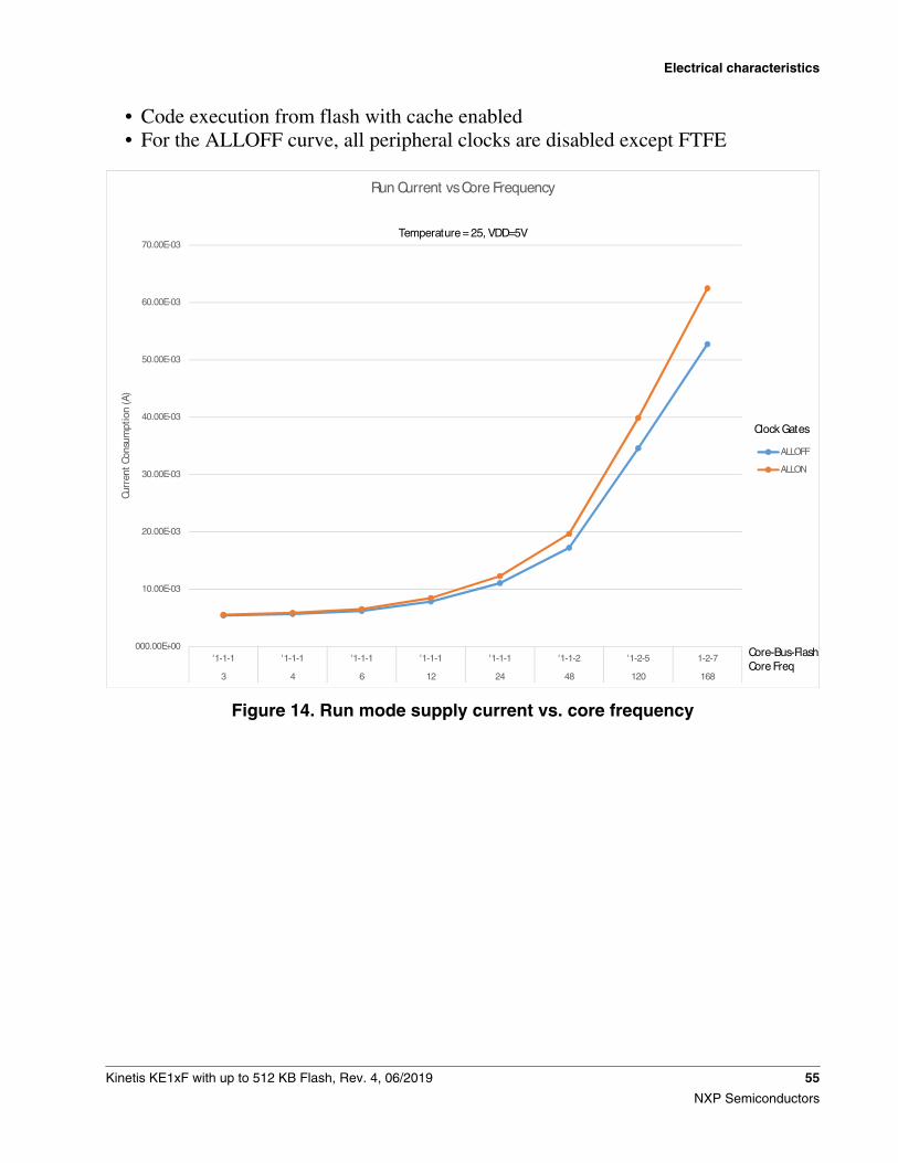
• Code execution from flash with cache enabled• For the ALLOFF curve, all peripheral clocks are disabled except FTFE
000.00E+00
10.00E-03
20.00E-03
30.00E-03
40.00E-03
50.00E-03
60.00E-03
70.00E-03
'1-1-1 '1-1-1 '1-1-1 '1-1-1 '1-1-1 '1-1-2 '1-2-5 1-2-7 3 4 6 12 24 48 120 168
Curr
ent C
onsu
mpt
ion
(A)
Run Current vs Core Frequency
ALLOFF
ALLON
Clock Gates
Temperature = 25, VDD=5V
Core-Bus-Flash Core Freq
Figure 14. Run mode supply current vs. core frequency
Electrical characteristics
Kinetis KE1xF with up to 512 KB Flash, Rev. 4, 06/2019 55
NXP Semiconductors
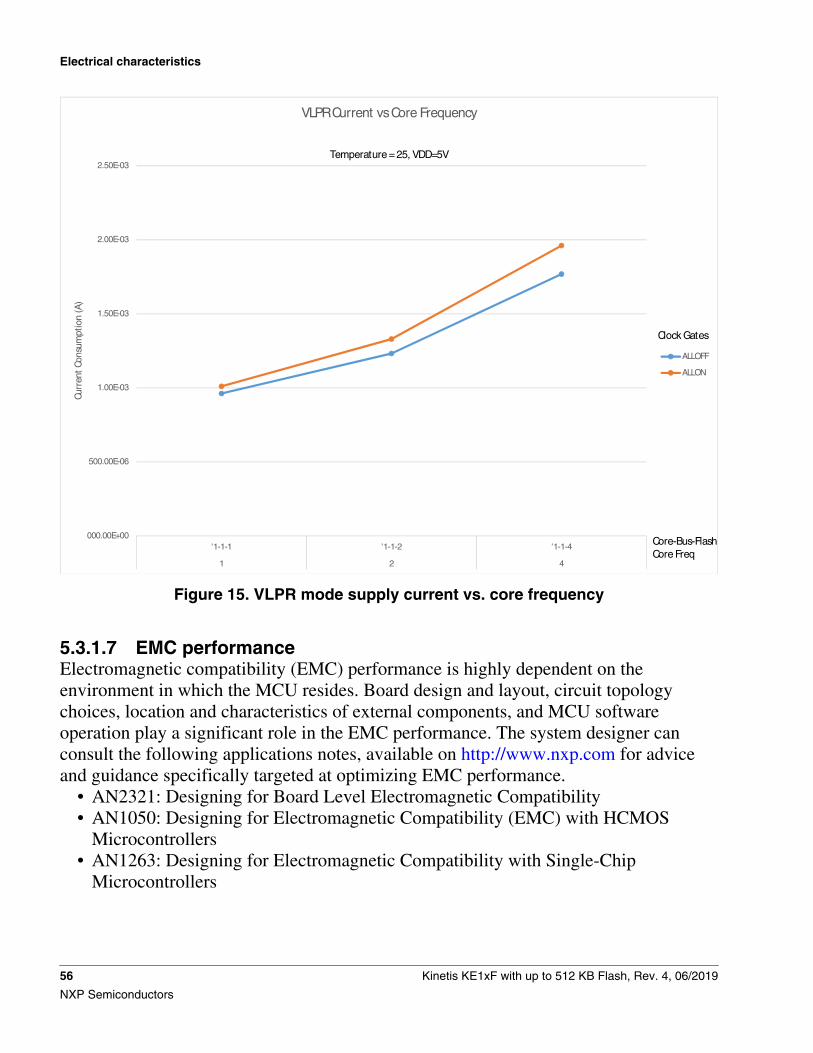
000.00E+00
500.00E-06
1.00E-03
1.50E-03
2.00E-03
2.50E-03
'1-1-1 '1-1-2 '1-1-4 1 2 4
Curr
ent C
onsu
mpt
ion
(A)
VLPR Current vs Core Frequency
ALLOFF
ALLON
Clock Gates
Temperature = 25, VDD=5V
Core-Bus-Flash Core Freq
Figure 15. VLPR mode supply current vs. core frequency
5.3.1.7 EMC performanceElectromagnetic compatibility (EMC) performance is highly dependent on theenvironment in which the MCU resides. Board design and layout, circuit topologychoices, location and characteristics of external components, and MCU softwareoperation play a significant role in the EMC performance. The system designer canconsult the following applications notes, available on http://www.nxp.com for adviceand guidance specifically targeted at optimizing EMC performance.
• AN2321: Designing for Board Level Electromagnetic Compatibility• AN1050: Designing for Electromagnetic Compatibility (EMC) with HCMOS
Microcontrollers• AN1263: Designing for Electromagnetic Compatibility with Single-Chip
Microcontrollers
Electrical characteristics
56 Kinetis KE1xF with up to 512 KB Flash, Rev. 4, 06/2019
NXP Semiconductors
• AN2764: Improving the Transient Immunity Performance of Microcontroller-Based Applications
• AN1259: System Design and Layout Techniques for Noise Reduction in MCU-Based Systems
5.3.1.7.1 EMC radiated emissions operating behaviors
EMC measurements to IC-level IEC standards are available from NXP on request.
5.3.1.7.2 Designing with radiated emissions in mind
To find application notes that provide guidance on designing your system to minimizeinterference from radiated emissions.
1. Go to http://www.nxp.com.2. Perform a keyword search for “EMC design”.3. Select the "Documents" category and find the application notes.
5.3.1.8 Capacitance attributesTable 33. Capacitance attributes
Symbol Description Min. Max. Unit
CIN_A Input capacitance: analog pins — 7 pF
CIN_D Input capacitance: digital pins — 7 pF
NOTEPlease refer to External Oscillator electrical specificationsfor EXTAL/XTAL pins.
5.3.2 Switching specifications
5.3.2.1 Device clock specifications
Table 34. Device clock specifications
Symbol Description Min. Max. Unit Notes
High Speed RUN mode
fSYS System and core clock — 168 MHz
fBUS Bus clock — 84 MHz
Table continues on the next page...
Electrical characteristics
Kinetis KE1xF with up to 512 KB Flash, Rev. 4, 06/2019 57
NXP Semiconductors
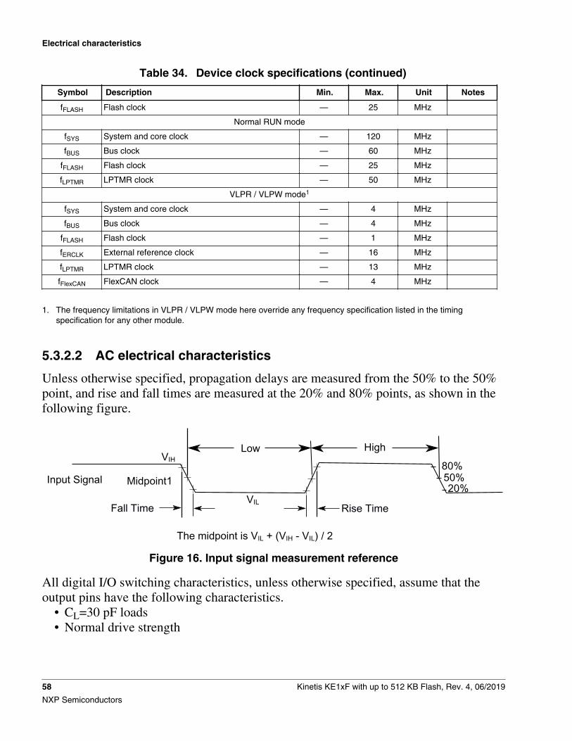
Table 34. Device clock specifications (continued)
Symbol Description Min. Max. Unit Notes
fFLASH Flash clock — 25 MHz
Normal RUN mode
fSYS System and core clock — 120 MHz
fBUS Bus clock — 60 MHz
fFLASH Flash clock — 25 MHz
fLPTMR LPTMR clock — 50 MHz
VLPR / VLPW mode1
fSYS System and core clock — 4 MHz
fBUS Bus clock — 4 MHz
fFLASH Flash clock — 1 MHz
fERCLK External reference clock — 16 MHz
fLPTMR LPTMR clock — 13 MHz
fFlexCAN FlexCAN clock — 4 MHz
1. The frequency limitations in VLPR / VLPW mode here override any frequency specification listed in the timingspecification for any other module.
5.3.2.2 AC electrical characteristics
Unless otherwise specified, propagation delays are measured from the 50% to the 50%point, and rise and fall times are measured at the 20% and 80% points, as shown in thefollowing figure.
80%
20%50%
VIL
Input Signal
VIH
Fall Time
HighLow
Rise Time
Midpoint1
The midpoint is VIL + (VIH - VIL) / 2
Figure 16. Input signal measurement reference
All digital I/O switching characteristics, unless otherwise specified, assume that theoutput pins have the following characteristics.
• CL=30 pF loads• Normal drive strength
Electrical characteristics
58 Kinetis KE1xF with up to 512 KB Flash, Rev. 4, 06/2019
NXP Semiconductors
5.3.2.3 General AC specifications
These general purpose specifications apply to all signals configured for GPIO, UART,and timers.
Table 35. General switching specifications
Symbol Description Min. Max. Unit Notes
GPIO pin interrupt pulse width (digital glitch filterdisabled) — Synchronous path
1.5 — Bus clockcycles
1, 2
External RESET and NMI pin interrupt pulse width —Asynchronous path
100 — ns 3
GPIO pin interrupt pulse width (digital glitch filterdisabled, passive filter disabled) — Asynchronouspath
50 — ns 4
1. This is the minimum pulse width that is guaranteed to pass through the pin synchronization circuitry. Shorter pulsesmay or may not be recognized. In Stop and VLPS modes, the synchronizer is bypassed so shorter pulses can berecognized in that case.
2. The greater of synchronous and asynchronous timing must be met.3. These pins have a passive filter enabled on the inputs. This is the shortest pulse width that is guaranteed to be
recognized.4. These pins do not have a passive filter on the inputs. This is the shortest pulse width that is guaranteed to be
recognized.
5.3.2.4 AC specifications at 3.3 V rangeTable 36. Functional pad AC specifications
Characteristic Symbol Min Typ Max Unit
I/O Supply Voltage Vdd 1 2.7 4 V
1. Max power supply ramp rate is 500 V/ms.
Name Prop Delay (ns) 1 Rise/Fall Edge (ns) 2 Drive Load (pF)
Max Min Max
Normal drive I/O pad 17.5 5 17 25
28 9 32 50
High drive I/O pad 19 5 17 25
26 9 33 50
CMOS Input 3 4 1.2 3 0.5
1. Propagation delay measured from 50% of core side input to 50% of the output.2. Edges measured using 20% and 80% of the VDD supply.3. Input slope = 2 ns.
NOTEAll measurements were taken accounting for 150 mV dropacross VDD and VSS.
Electrical characteristics
Kinetis KE1xF with up to 512 KB Flash, Rev. 4, 06/2019 59
NXP Semiconductors
5.3.2.5 AC specifications at 5 V rangeTable 37. Functional pad AC specifications
Characteristic Symbol Min Typ Max Unit
I/O Supply Voltage Vdd 1 4 5.5 V
1. Max power supply ramp rate is 500 V/ms.
Name Prop Delay (ns) 1 Rise/Fall Edge (ns) 2 Drive Load (pF)
Max Min Max
Normal drive I/O pad 12 3.6 10 25
18 8 17 50
High drive I/O pad 13 3.6 10 25
19 8 19 50
CMOS Input 3 3 1.2 2.8 0.5
1. As measured from 50% of core side input to 50% of the output.2. Edges measured using 20% and 80% of the VDD supply.3. Input slope = 2 ns.
NOTEAll measurements were taken accounting for 150 mV dropacross VDD and VSS.
5.3.3 Thermal specifications
5.3.3.1 Thermal operating requirementsTable 38. Thermal operating requirements
Symbol Description Min. Max. Unit Notes
TJ Die junction temperature –40 125 °C
TA Ambient temperature –40 105 °C 1
1. Maximum TA can be exceeded only if the user ensures that TJ does not exceed maximum TJ. The simplest method todetermine TJ is: TJ = TA + RΘJA × chip power dissipation.
5.3.3.2 Thermal attributes
Electrical characteristics
60 Kinetis KE1xF with up to 512 KB Flash, Rev. 4, 06/2019
NXP Semiconductors
5.3.3.2.1 Description
The tables in the following sections describe the thermal characteristics of the device.
NOTEJunction temperature is a function of die size, on-chip powerdissipation, package thermal resistance, mounting side(board) temperature, ambient temperature, air flow, powerdissipation or other components on the board, and boardthermal resistance.
5.3.3.2.2 Thermal characteristics for the 64-pin LQFP packageTable 39. Thermal characteristics for the 64-pin LQFP package
Rating Conditions Symbol Value Unit
Thermal resistance, Junction to Ambient(Natural Convection)1, 2
Single layer board (1s) RθJA 60 °C/W
Thermal resistance, Junction to Ambient(Natural Convection)1, 2
Four layer board (2s2p) RθJA 42 °C/W
Thermal resistance, Junction to Ambient(@200 ft/min)1, 3
Single layer board (1s) RθJMA 49 °C/W
Thermal resistance, Junction to Ambient(@200 ft/min)1, 3
Four layer board (2s2p) RθJMA 36 °C/W
Thermal resistance, Junction to Board4 — RθJB 24 °C/W
Thermal resistance, Junction to Case 5 — RθJC 12 °C/W
Thermal resistance, Junction to Package Top6 Natural Convection ψJT 2 °C/W
1. Junction temperature is a function of die size, on-chip power dissipation, package thermal resistance, mounting site(board) temperature, ambient temperature, air flow, power dissipation of other components on the board, and boardthermal resistance.
2. Per JEDEC JESD51-2 with natural convection for horizontally oriented board. Board meets JESD51-9 specification for1s or 2s2p board, respectively.
3. Per JEDEC JESD51-6 with forced convection for horizontally oriented board. Board meets JESD51-9 specification for1s or 2s2p board, respectively.
4. Thermal resistance between the die and the printed circuit board per JEDEC JESD51-8. Board temperature ismeasured on the top surface of the board near the package.
5. Thermal resistance between the die and the case top surface as measured by the cold plate method (MIL SPEC-883Method 1012.1).
6. Thermal characterization parameter indicating the temperature difference between package top and the junctiontemperature per JEDEC JESD51-2.
5.3.3.2.3 Thermal characteristics for the 100-pin LQFP packageTable 40. Thermal characteristics for the 100-pin LQFP package
Rating Conditions Symbol Value Unit
Thermal resistance, Junction to Ambient(Natural Convection)1, 2
Single layer board (1s) RθJA 57 °C/W
Table continues on the next page...
Electrical characteristics
Kinetis KE1xF with up to 512 KB Flash, Rev. 4, 06/2019 61
NXP Semiconductors
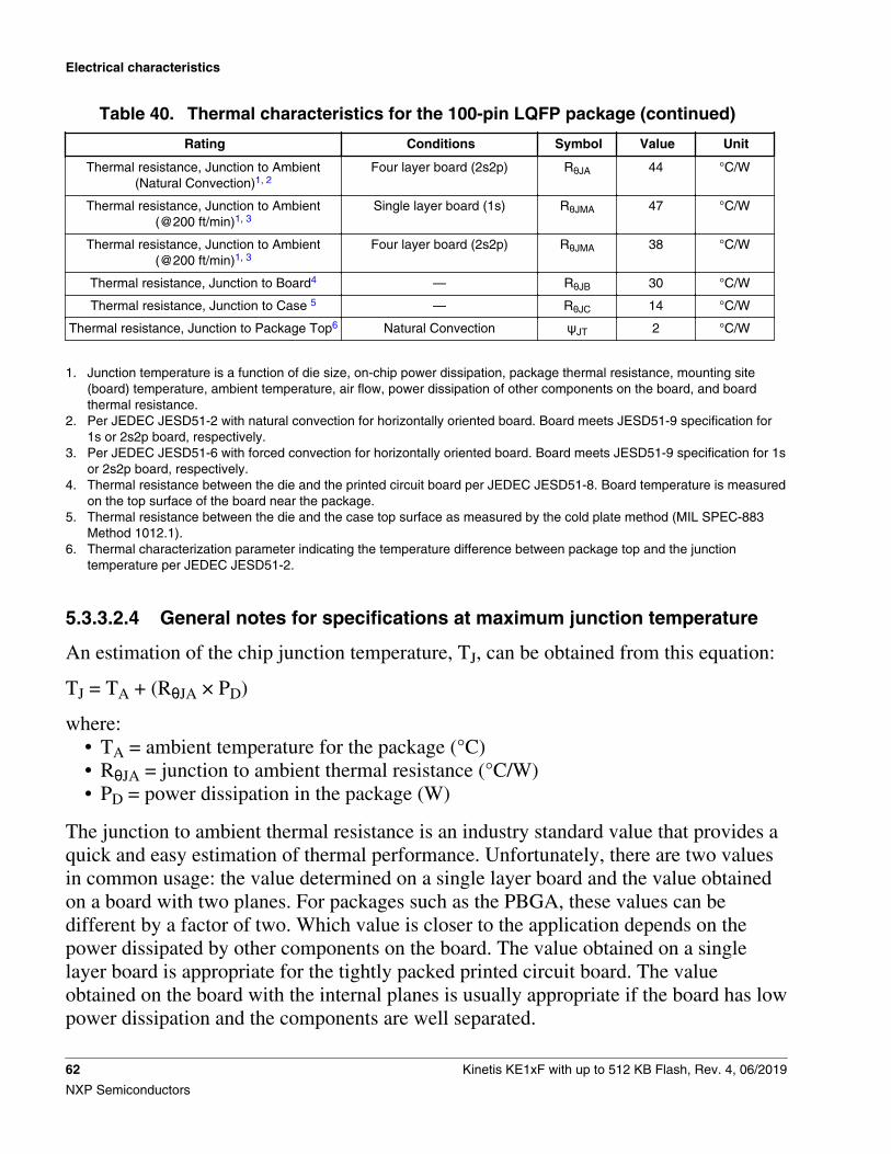
Table 40. Thermal characteristics for the 100-pin LQFP package (continued)
Rating Conditions Symbol Value Unit
Thermal resistance, Junction to Ambient(Natural Convection)1, 2
Four layer board (2s2p) RθJA 44 °C/W
Thermal resistance, Junction to Ambient(@200 ft/min)1, 3
Single layer board (1s) RθJMA 47 °C/W
Thermal resistance, Junction to Ambient(@200 ft/min)1, 3
Four layer board (2s2p) RθJMA 38 °C/W
Thermal resistance, Junction to Board4 — RθJB 30 °C/W
Thermal resistance, Junction to Case 5 — RθJC 14 °C/W
Thermal resistance, Junction to Package Top6 Natural Convection ψJT 2 °C/W
1. Junction temperature is a function of die size, on-chip power dissipation, package thermal resistance, mounting site(board) temperature, ambient temperature, air flow, power dissipation of other components on the board, and boardthermal resistance.
2. Per JEDEC JESD51-2 with natural convection for horizontally oriented board. Board meets JESD51-9 specification for1s or 2s2p board, respectively.
3. Per JEDEC JESD51-6 with forced convection for horizontally oriented board. Board meets JESD51-9 specification for 1sor 2s2p board, respectively.
4. Thermal resistance between the die and the printed circuit board per JEDEC JESD51-8. Board temperature is measuredon the top surface of the board near the package.
5. Thermal resistance between the die and the case top surface as measured by the cold plate method (MIL SPEC-883Method 1012.1).
6. Thermal characterization parameter indicating the temperature difference between package top and the junctiontemperature per JEDEC JESD51-2.
5.3.3.2.4 General notes for specifications at maximum junction temperature
An estimation of the chip junction temperature, TJ, can be obtained from this equation:
TJ = TA + (RθJA × PD)
where:• TA = ambient temperature for the package (°C)• RθJA = junction to ambient thermal resistance (°C/W)• PD = power dissipation in the package (W)
The junction to ambient thermal resistance is an industry standard value that provides aquick and easy estimation of thermal performance. Unfortunately, there are two valuesin common usage: the value determined on a single layer board and the value obtainedon a board with two planes. For packages such as the PBGA, these values can bedifferent by a factor of two. Which value is closer to the application depends on thepower dissipated by other components on the board. The value obtained on a singlelayer board is appropriate for the tightly packed printed circuit board. The valueobtained on the board with the internal planes is usually appropriate if the board has lowpower dissipation and the components are well separated.
Electrical characteristics
62 Kinetis KE1xF with up to 512 KB Flash, Rev. 4, 06/2019
NXP Semiconductors
When a heat sink is used, the thermal resistance is expressed in the following equationas the sum of a junction-to-case thermal resistance and a case-to-ambient thermalresistance:
RθJA = RθJC + RθCA
where:• RθJA = junction to ambient thermal resistance (°C/W)• RθJC = junction to case thermal resistance (°C/W)• RθCA = case to ambient thermal resistance (°C/W)
RθJC is device related and cannot be influenced by the user. The user controls thethermal environment to change the case to ambient thermal resistance, RθCA. Forinstance, the user can change the size of the heat sink, the air flow around the device,the interface material, the mounting arrangement on printed circuit board, or changethe thermal dissipation on the printed circuit board surrounding the device.
To determine the junction temperature of the device in the application when heat sinksare not used, the Thermal Characterization Parameter (ΨJT) can be used to determinethe junction temperature with a measurement of the temperature at the top center ofthe package case using this equation:
TJ = TT + (ΨJT × PD)
where:• TT = thermocouple temperature on top of the package (°C)• ΨJT = thermal characterization parameter (°C/W)• PD = power dissipation in the package (W)
The thermal characterization parameter is measured per JESD51-2 specification usinga 40 gauge type T thermocouple epoxied to the top center of the package case. Thethermocouple should be positioned so that the thermocouple junction rests on thepackage. A small amount of epoxy is placed over the thermocouple junction and overabout 1 mm of wire extending from the junction. The thermocouple wire is placed flatagainst the package case to avoid measurement errors caused by cooling effects of thethermocouple wire.
5.4 Peripheral operating requirements and behaviors
Electrical characteristics
Kinetis KE1xF with up to 512 KB Flash, Rev. 4, 06/2019 63
NXP Semiconductors
5.4.1 System modules
There are no specifications necessary for the device's system modules.
5.4.2 Clock interface modules
5.4.2.1 Oscillator electrical specifications
5.4.2.1.1 External Oscillator electrical specifications
Electrical characteristics
64 Kinetis KE1xF with up to 512 KB Flash, Rev. 4, 06/2019
NXP Semiconductors
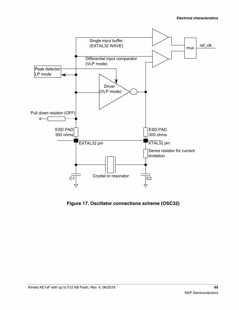
Single input buffer(EXTAL32 WAVE) mux ref_clk
Differential input comparator(VLP mode)
Peak detectorLP mode
Driver(VLP mode)
Pull down resistor (OFF)
ESD PAD300 ohms
ESD PAD300 ohms
EXTAL32 pin XTAL32 pin
Series resistor for current limitation
Crystal or resonatorC1 C2
Figure 17. Oscillator connections scheme (OSC32)
Electrical characteristics
Kinetis KE1xF with up to 512 KB Flash, Rev. 4, 06/2019 65
NXP Semiconductors
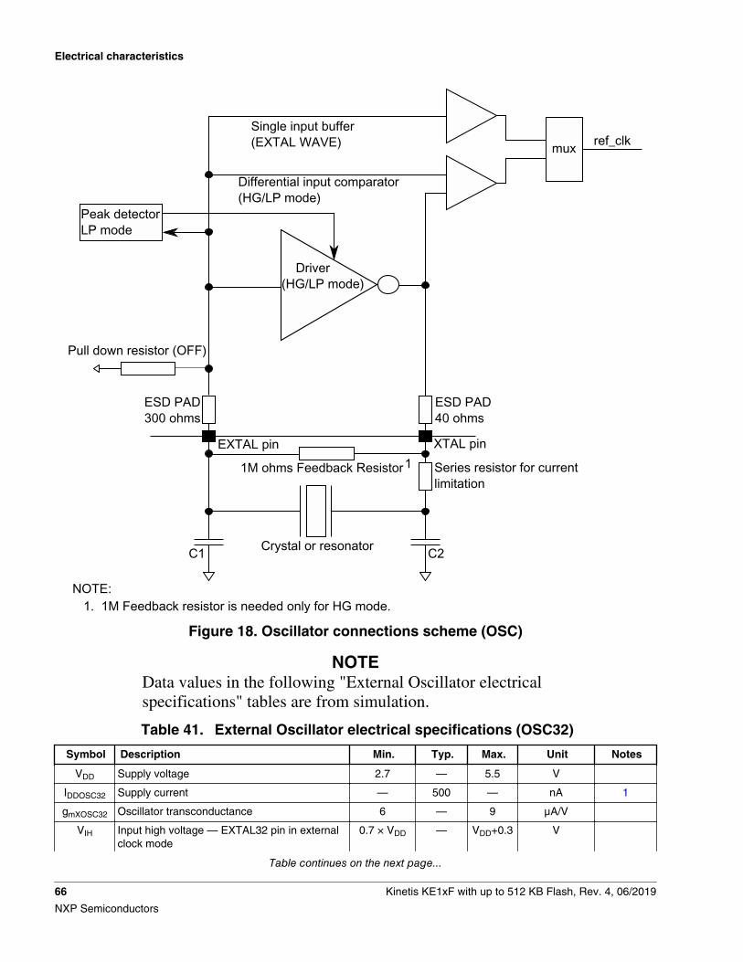
Single input buffer(EXTAL WAVE) mux ref_clk
Differential input comparator(HG/LP mode)
Peak detectorLP mode
Driver(HG/LP mode)
Pull down resistor (OFF)
ESD PAD300 ohms
ESD PAD40 ohms
EXTAL pin XTAL pin
Series resistor for current limitation
Crystal or resonatorC1 C2
1M ohms Feedback Resistor1
NOTE:1. 1M Feedback resistor is needed only for HG mode.
Figure 18. Oscillator connections scheme (OSC)
NOTEData values in the following "External Oscillator electricalspecifications" tables are from simulation.
Table 41. External Oscillator electrical specifications (OSC32)
Symbol Description Min. Typ. Max. Unit Notes
VDD Supply voltage 2.7 — 5.5 V
IDDOSC32 Supply current — 500 — nA 1
gmXOSC32 Oscillator transconductance 6 — 9 µA/V
VIH Input high voltage — EXTAL32 pin in externalclock mode
0.7 × VDD — VDD+0.3 V
Table continues on the next page...
Electrical characteristics
66 Kinetis KE1xF with up to 512 KB Flash, Rev. 4, 06/2019
NXP Semiconductors
Table 41. External Oscillator electrical specifications (OSC32) (continued)
Symbol Description Min. Typ. Max. Unit Notes
@VDD=3.3 V
@VDD=5.0 V 0.65 × VDD — VDD+0.3 V
VIL Input low voltage — EXTAL32 pin in externalclock mode
@VDD=3.3 V
VSS –0.3 — 0.3 ×VDD
V
@VDD=5.0 V VSS –0.3 — 0.35 ×VDD
V
C1 EXTAL32 load capacitance — — — 2
C2 XTAL32 load capacitance — — — 2
RF Feedback resistor — — — MΩ
RS Series resistor — — — kΩ
Vpp_OSC32 Peak-to-peak amplitude of oscillation (oscillatormode)
— 0.6 — V 3
1. Measured at VDD = 5 V, Temperature = 25 °C. The current consumption is according to the crystal or resonator,loading capacitance.
2. C1 and C2 must be provided by external capacitors and their load capacitance depends on the crystal or resonatormanufacturers' recommendation. Please check the crystal datasheet for the recommended values. And also considerthe parasitic capacitance of package and board.
3. The EXTAL32 and XTAL32 pins should only be connected to required oscillator components and must not beconnected to any other devices.
Table 42. External Oscillator electrical specifications (OSC)
Symbol Description Min. Typ. Max. Unit Notes
VDD Supply voltage 2.7 — 5.5 V
IDDOSC Supply current — low-gain mode (low-power mode) (HGO=0) 1
4 MHz — 200 — µA
8 MHz — 300 — µA
16 MHz — 1.2 — mA
24 MHz — 1.6 — mA
32 MHz — 2 — mA
40 MHz — 2.6 — mA
IDDOSC Supply current — high-gain mode (HGO=1) 1
32 kHz — 25 — µA
4 MHz — 1 — mA
8 MHz — 1.2 — mA
16 MHz — 3.5 — mA
24 MHz — 5 — mA
32 MHz — 5.5 — mA
40 MHz — 6 — mA
gmXOSC Fast external crystal oscillator transconductance
Table continues on the next page...
Electrical characteristics
Kinetis KE1xF with up to 512 KB Flash, Rev. 4, 06/2019 67
NXP Semiconductors
Table 42. External Oscillator electrical specifications (OSC)(continued)
Symbol Description Min. Typ. Max. Unit Notes
32 kHz, Low Frequency Range, High Gain (32 kHz) 15 — 45 µA / V
Medium Frequency Range (4-8 MHz) 2.2 — 9.7 mA / V
High Frequency Range (8-40 MHz) 16 37 mA / V
VIH Input high voltage — EXTAL pin in external clockmode
1.75 — VDD V
VIL Input low voltage — EXTAL pin in external clockmode
VSS — 1.20 V
C1 EXTAL load capacitance — — — 2
C2 XTAL load capacitance — — — 2
RF Feedback resistor 3
Low-frequency, high-gain mode (32 kHz) — 10 — MΩ
Medium/high-frequency, low-gain mode (low-powermode) (4-8 MHz, 8-40 MHz)
— — — MΩ
Medium/high-frequency, high-gain mode (4-8 MHz,8-40 MHz)
— 1 — MΩ
RS Series resistor
Low-frequency, high-gain mode (32 kHz) — 200 — kΩ
Medium/high-frequency, low-gain mode (low-powermode) (4-8 MHz, 8-40 MHz)
— 0 — kΩ
Medium/high-frequency, high-gain mode (4-8 MHz,8-40 MHz)
— 0 — kΩ
Vpp Peak-to-peak amplitude of oscillation (oscillator mode) 4
Low-frequency, high-gain mode — 3.3 — V
Medium/high-frequency, low-gain mode — 1.0 — V
Medium/high-frequency, high-gain mode — 3.3 — V
1. Measured at VDD = 5 V, Temperature = 25 °C. The current consumption is according to the crystal or resonator, loadingcapacitance.
2. C1 and C2 must be provided by external capacitors and their load capacitance depends on the crystal or resonatormanufacturers' recommendation. Please check the crystal datasheet for the recommended values. And also considerthe parasitic capacitance of package and board.
3. When low power mode is selected, RF is integrated and must not be attached externally.4. The EXTAL and XTAL pins should only be connected to required oscillator components and must not be connected to
any other devices.
5.4.2.1.2 External Oscillator frequency specificationsTable 43. External Oscillator frequency specifications (OSC32)
Symbol Description Min. Typ. Max. Unit Notes
fosc32_lo Oscillator crystal or resonator frequency — low-frequency mode
30 — 40 kHz
tdc_extal32 Input clock duty cycle (external clock mode) 40 50 60 %
Table continues on the next page...
Electrical characteristics
68 Kinetis KE1xF with up to 512 KB Flash, Rev. 4, 06/2019
NXP Semiconductors
Table 43. External Oscillator frequency specifications (OSC32) (continued)
Symbol Description Min. Typ. Max. Unit Notes
fec_extal32 Input clock frequency (external clock mode) — — 40 kHz
tcst32 Crystal startup time — 32 kHz low-frequency,low-power mode (HGO=0)
— 2000 — ms 1
1. The start-up measured after 4096 cycles. Proper PC board layout procedures must be followed to achievespecifications.
Table 44. External Oscillator frequency specifications (OSC)
Symbol Description Min. Typ. Max. Unit Notes
fosc_lo Oscillator crystal or resonator frequency — LowFrequency, High Gain Mode
32 — 40 kHz
fosc_me Oscillator crystal or resonator frequency —Medium Frequency
4 — 8 MHz
fosc_hi Oscillator crystal or resonator frequency —High Frequency
8 — 40
tdc_extal Input clock duty cycle (external clock mode) 40 50 60 %
fec_extal Input clock frequency (external clock mode) — — 50 MHz
tcst Crystal startup time — 32 kHz Low Frequency,High-Gain Mode
— 500 — ms 1
Crystal startup time — 8 MHz MediumFrequency, Low-Power Mode
— 1.5 —
Crystal startup time — 8 MHz MediumFrequency, High-Gain Mode
— 2.5 —
Crystal startup time — 40 MHz HighFrequency, Low-Power Mode
— 2 —
Crystal startup time — 40 MHz HighFrequency, High-Gain Mode
— 2.5 —
1. The start-up measured after 4096 cycles. Proper PC board layout procedures must be followed to achievespecifications.
5.4.2.2 System Clock Generation (SCG) specifications
5.4.2.2.1 Fast internal RC Oscillator (FIRC) electrical specificationsTable 45. Fast internal RC Oscillator electrical specifications
Symbol Parameter Value Unit
Min. Typ. Max.
FFIRC Fast internal reference frequency —48
— MHz
IVDD Supply current — 400 500 µA
Table continues on the next page...
Electrical characteristics
Kinetis KE1xF with up to 512 KB Flash, Rev. 4, 06/2019 69
NXP Semiconductors
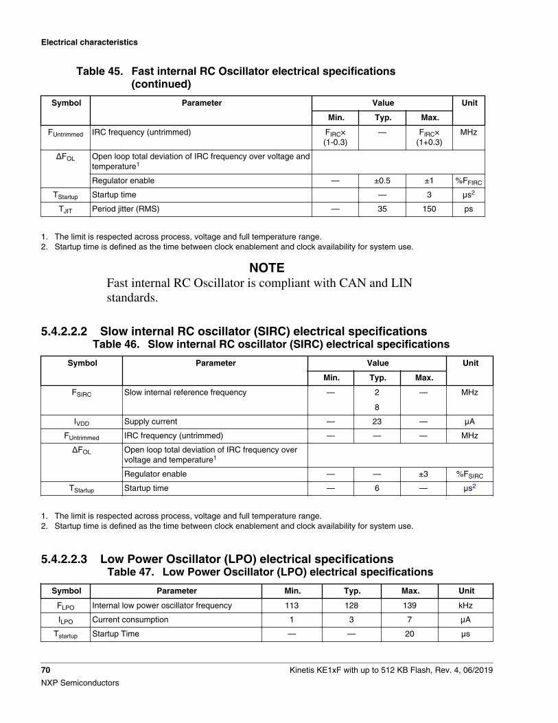
Table 45. Fast internal RC Oscillator electrical specifications(continued)
Symbol Parameter Value Unit
Min. Typ. Max.
FUntrimmed IRC frequency (untrimmed) FIRC×(1-0.3)
— FIRC×(1+0.3)
MHz
ΔFOL Open loop total deviation of IRC frequency over voltage andtemperature1
Regulator enable — ±0.5 ±1 %FFIRC
TStartup Startup time — 3 µs2
TJIT Period jitter (RMS) — 35 150 ps
1. The limit is respected across process, voltage and full temperature range.2. Startup time is defined as the time between clock enablement and clock availability for system use.
NOTEFast internal RC Oscillator is compliant with CAN and LINstandards.
5.4.2.2.2 Slow internal RC oscillator (SIRC) electrical specificationsTable 46. Slow internal RC oscillator (SIRC) electrical specifications
Symbol Parameter Value Unit
Min. Typ. Max.
FSIRC Slow internal reference frequency — 2
8
— MHz
IVDD Supply current — 23 — µA
FUntrimmed IRC frequency (untrimmed) — — — MHz
ΔFOL Open loop total deviation of IRC frequency overvoltage and temperature1
Regulator enable — — ±3 %FSIRC
TStartup Startup time — 6 — µs2
1. The limit is respected across process, voltage and full temperature range.2. Startup time is defined as the time between clock enablement and clock availability for system use.
5.4.2.2.3 Low Power Oscillator (LPO) electrical specificationsTable 47. Low Power Oscillator (LPO) electrical specifications
Symbol Parameter Min. Typ. Max. Unit
FLPO Internal low power oscillator frequency 113 128 139 kHz
ILPO Current consumption 1 3 7 µA
Tstartup Startup Time — — 20 µs
Electrical characteristics
70 Kinetis KE1xF with up to 512 KB Flash, Rev. 4, 06/2019
NXP Semiconductors
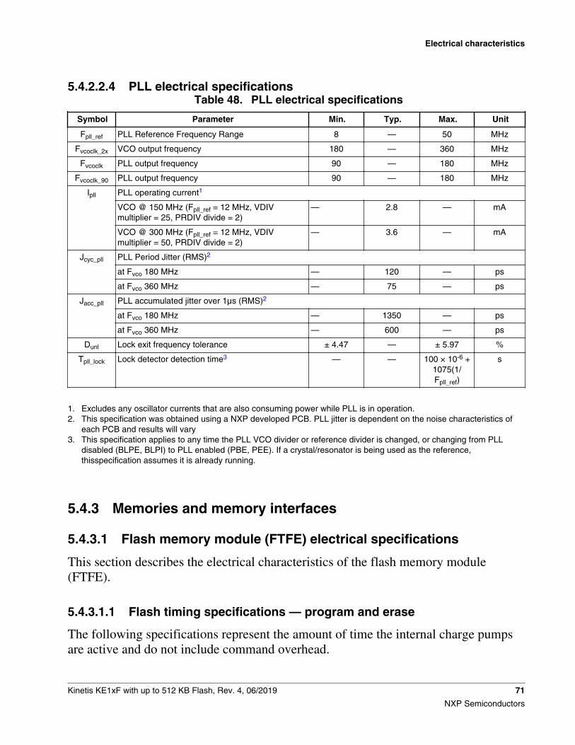
5.4.2.2.4 PLL electrical specificationsTable 48. PLL electrical specifications
Symbol Parameter Min. Typ. Max. Unit
Fpll_ref PLL Reference Frequency Range 8 — 50 MHz
Fvcoclk_2x VCO output frequency 180 — 360 MHz
Fvcoclk PLL output frequency 90 — 180 MHz
Fvcoclk_90 PLL output frequency 90 — 180 MHz
Ipll PLL operating current1
VCO @ 150 MHz (Fpll_ref = 12 MHz, VDIVmultiplier = 25, PRDIV divide = 2)
— 2.8 — mA
VCO @ 300 MHz (Fpll_ref = 12 MHz, VDIVmultiplier = 50, PRDIV divide = 2)
— 3.6 — mA
Jcyc_pll PLL Period Jitter (RMS)2
at Fvco 180 MHz — 120 — ps
at Fvco 360 MHz — 75 — ps
Jacc_pll PLL accumulated jitter over 1µs (RMS)2
at Fvco 180 MHz — 1350 — ps
at Fvco 360 MHz — 600 — ps
Dunl Lock exit frequency tolerance ± 4.47 — ± 5.97 %
Tpll_lock Lock detector detection time3 — — 100 × 10-6 +1075(1/Fpll_ref)
s
1. Excludes any oscillator currents that are also consuming power while PLL is in operation.2. This specification was obtained using a NXP developed PCB. PLL jitter is dependent on the noise characteristics of
each PCB and results will vary3. This specification applies to any time the PLL VCO divider or reference divider is changed, or changing from PLL
disabled (BLPE, BLPI) to PLL enabled (PBE, PEE). If a crystal/resonator is being used as the reference,thisspecification assumes it is already running.
5.4.3 Memories and memory interfaces
5.4.3.1 Flash memory module (FTFE) electrical specifications
This section describes the electrical characteristics of the flash memory module(FTFE).
5.4.3.1.1 Flash timing specifications — program and erase
The following specifications represent the amount of time the internal charge pumpsare active and do not include command overhead.
Electrical characteristics
Kinetis KE1xF with up to 512 KB Flash, Rev. 4, 06/2019 71
NXP Semiconductors
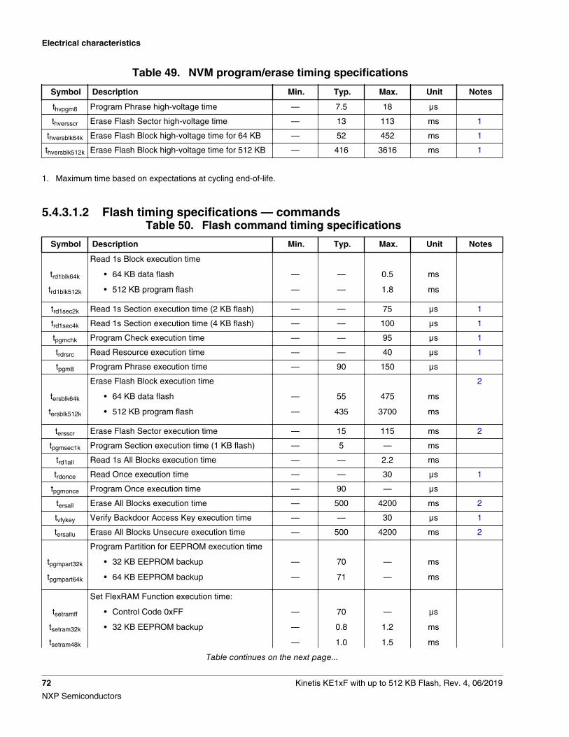
Table 49. NVM program/erase timing specifications
Symbol Description Min. Typ. Max. Unit Notes
thvpgm8 Program Phrase high-voltage time — 7.5 18 μs
thversscr Erase Flash Sector high-voltage time — 13 113 ms 1
thversblk64k Erase Flash Block high-voltage time for 64 KB — 52 452 ms 1
thversblk512k Erase Flash Block high-voltage time for 512 KB — 416 3616 ms 1
1. Maximum time based on expectations at cycling end-of-life.
5.4.3.1.2 Flash timing specifications — commandsTable 50. Flash command timing specifications
Symbol Description Min. Typ. Max. Unit Notes
trd1blk64k
trd1blk512k
Read 1s Block execution time
• 64 KB data flash
• 512 KB program flash
—
—
—
—
0.5
1.8
ms
ms
trd1sec2k Read 1s Section execution time (2 KB flash) — — 75 μs 1
trd1sec4k Read 1s Section execution time (4 KB flash) — — 100 μs 1
tpgmchk Program Check execution time — — 95 μs 1
trdrsrc Read Resource execution time — — 40 μs 1
tpgm8 Program Phrase execution time — 90 150 μs
tersblk64k
tersblk512k
Erase Flash Block execution time
• 64 KB data flash
• 512 KB program flash
—
—
55
435
475
3700
ms
ms
2
tersscr Erase Flash Sector execution time — 15 115 ms 2
tpgmsec1k Program Section execution time (1 KB flash) — 5 — ms
trd1all Read 1s All Blocks execution time — — 2.2 ms
trdonce Read Once execution time — — 30 μs 1
tpgmonce Program Once execution time — 90 — μs
tersall Erase All Blocks execution time — 500 4200 ms 2
tvfykey Verify Backdoor Access Key execution time — — 30 μs 1
tersallu Erase All Blocks Unsecure execution time — 500 4200 ms 2
tpgmpart32k
tpgmpart64k
Program Partition for EEPROM execution time
• 32 KB EEPROM backup
• 64 KB EEPROM backup
—
—
70
71
—
—
ms
ms
tsetramff
tsetram32k
tsetram48k
Set FlexRAM Function execution time:
• Control Code 0xFF
• 32 KB EEPROM backup
—
—
—
70
0.8
1.0
—
1.2
1.5
μs
ms
ms
Table continues on the next page...
Electrical characteristics
72 Kinetis KE1xF with up to 512 KB Flash, Rev. 4, 06/2019
NXP Semiconductors
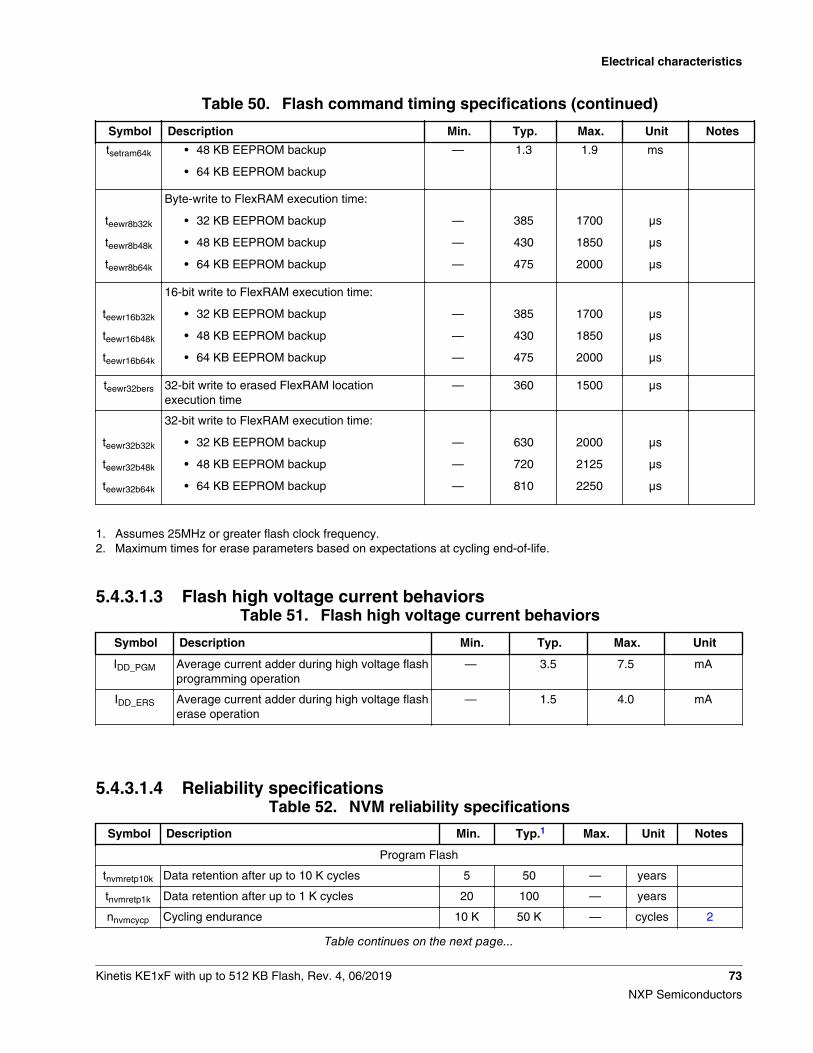
Table 50. Flash command timing specifications (continued)
Symbol Description Min. Typ. Max. Unit Notes
tsetram64k • 48 KB EEPROM backup
• 64 KB EEPROM backup
— 1.3 1.9 ms
teewr8b32k
teewr8b48k
teewr8b64k
Byte-write to FlexRAM execution time:
• 32 KB EEPROM backup
• 48 KB EEPROM backup
• 64 KB EEPROM backup
—
—
—
385
430
475
1700
1850
2000
μs
μs
μs
teewr16b32k
teewr16b48k
teewr16b64k
16-bit write to FlexRAM execution time:
• 32 KB EEPROM backup
• 48 KB EEPROM backup
• 64 KB EEPROM backup
—
—
—
385
430
475
1700
1850
2000
μs
μs
μs
teewr32bers 32-bit write to erased FlexRAM locationexecution time
— 360 1500 μs
teewr32b32k
teewr32b48k
teewr32b64k
32-bit write to FlexRAM execution time:
• 32 KB EEPROM backup
• 48 KB EEPROM backup
• 64 KB EEPROM backup
—
—
—
630
720
810
2000
2125
2250
μs
μs
μs
1. Assumes 25MHz or greater flash clock frequency.2. Maximum times for erase parameters based on expectations at cycling end-of-life.
5.4.3.1.3 Flash high voltage current behaviorsTable 51. Flash high voltage current behaviors
Symbol Description Min. Typ. Max. Unit
IDD_PGM Average current adder during high voltage flashprogramming operation
— 3.5 7.5 mA
IDD_ERS Average current adder during high voltage flasherase operation
— 1.5 4.0 mA
5.4.3.1.4 Reliability specificationsTable 52. NVM reliability specifications
Symbol Description Min. Typ.1 Max. Unit Notes
Program Flash
tnvmretp10k Data retention after up to 10 K cycles 5 50 — years
tnvmretp1k Data retention after up to 1 K cycles 20 100 — years
nnvmcycp Cycling endurance 10 K 50 K — cycles 2
Table continues on the next page...
Electrical characteristics
Kinetis KE1xF with up to 512 KB Flash, Rev. 4, 06/2019 73
NXP Semiconductors
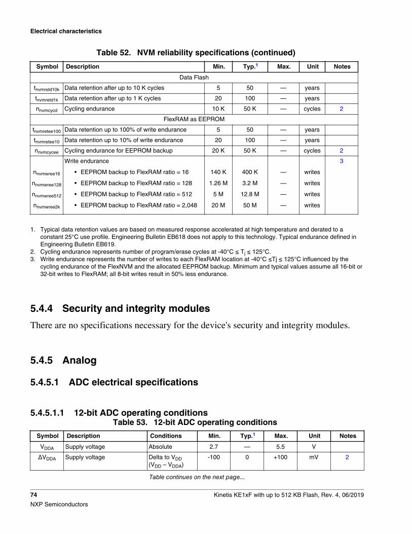
Table 52. NVM reliability specifications (continued)
Symbol Description Min. Typ.1 Max. Unit Notes
Data Flash
tnvmretd10k Data retention after up to 10 K cycles 5 50 — years
tnvmretd1k Data retention after up to 1 K cycles 20 100 — years
nnvmcycd Cycling endurance 10 K 50 K — cycles 2
FlexRAM as EEPROM
tnvmretee100 Data retention up to 100% of write endurance 5 50 — years
tnvmretee10 Data retention up to 10% of write endurance 20 100 — years
nnvmcycee Cycling endurance for EEPROM backup 20 K 50 K — cycles 2
nnvmwree16
nnvmwree128
nnvmwree512
nnvmwree2k
Write endurance
• EEPROM backup to FlexRAM ratio = 16
• EEPROM backup to FlexRAM ratio = 128
• EEPROM backup to FlexRAM ratio = 512
• EEPROM backup to FlexRAM ratio = 2,048
140 K
1.26 M
5 M
20 M
400 K
3.2 M
12.8 M
50 M
—
—
—
—
writes
writes
writes
writes
3
1. Typical data retention values are based on measured response accelerated at high temperature and derated to aconstant 25°C use profile. Engineering Bulletin EB618 does not apply to this technology. Typical endurance defined inEngineering Bulletin EB619.
2. Cycling endurance represents number of program/erase cycles at -40°C ≤ Tj ≤ 125°C.3. Write endurance represents the number of writes to each FlexRAM location at -40°C ≤Tj ≤ 125°C influenced by the
cycling endurance of the FlexNVM and the allocated EEPROM backup. Minimum and typical values assume all 16-bit or32-bit writes to FlexRAM; all 8-bit writes result in 50% less endurance.
5.4.4 Security and integrity modules
There are no specifications necessary for the device's security and integrity modules.
5.4.5 Analog
5.4.5.1 ADC electrical specifications
5.4.5.1.1 12-bit ADC operating conditionsTable 53. 12-bit ADC operating conditions
Symbol Description Conditions Min. Typ.1 Max. Unit Notes
VDDA Supply voltage Absolute 2.7 — 5.5 V
ΔVDDA Supply voltage Delta to VDD(VDD – VDDA)
-100 0 +100 mV 2
Table continues on the next page...
Electrical characteristics
74 Kinetis KE1xF with up to 512 KB Flash, Rev. 4, 06/2019
NXP Semiconductors
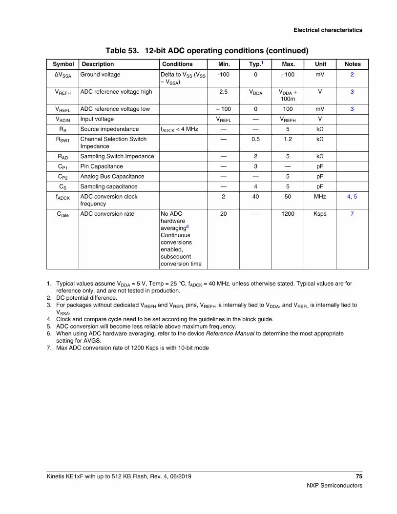
Table 53. 12-bit ADC operating conditions (continued)
Symbol Description Conditions Min. Typ.1 Max. Unit Notes
ΔVSSA Ground voltage Delta to VSS (VSS– VSSA)
-100 0 +100 mV 2
VREFH ADC reference voltage high 2.5 VDDA VDDA +100m
V 3
VREFL ADC reference voltage low − 100 0 100 mV 3
VADIN Input voltage VREFL — VREFH V
RS Source impedendance fADCK < 4 MHz — — 5 kΩ
RSW1 Channel Selection SwitchImpedance
— 0.5 1.2 kΩ
RAD Sampling Switch Impedance — 2 5 kΩ
CP1 Pin Capacitance — 3 — pF
CP2 Analog Bus Capacitance — — 5 pF
CS Sampling capacitance — 4 5 pF
fADCK ADC conversion clockfrequency
2 40 50 MHz 4, 5
Crate ADC conversion rate No ADChardwareaveraging6
Continuousconversionsenabled,subsequentconversion time
20 — 1200 Ksps 7
1. Typical values assume VDDA = 5 V, Temp = 25 °C, fADCK = 40 MHz, unless otherwise stated. Typical values are forreference only, and are not tested in production.
2. DC potential difference.3. For packages without dedicated VREFH and VREFL pins, VREFH is internally tied to VDDA, and VREFL is internally tied to
VSSA.4. Clock and compare cycle need to be set according the guidelines in the block guide.5. ADC conversion will become less reliable above maximum frequency.6. When using ADC hardware averaging, refer to the device Reference Manual to determine the most appropriate
setting for AVGS.7. Max ADC conversion rate of 1200 Ksps is with 10-bit mode
Electrical characteristics
Kinetis KE1xF with up to 512 KB Flash, Rev. 4, 06/2019 75
NXP Semiconductors
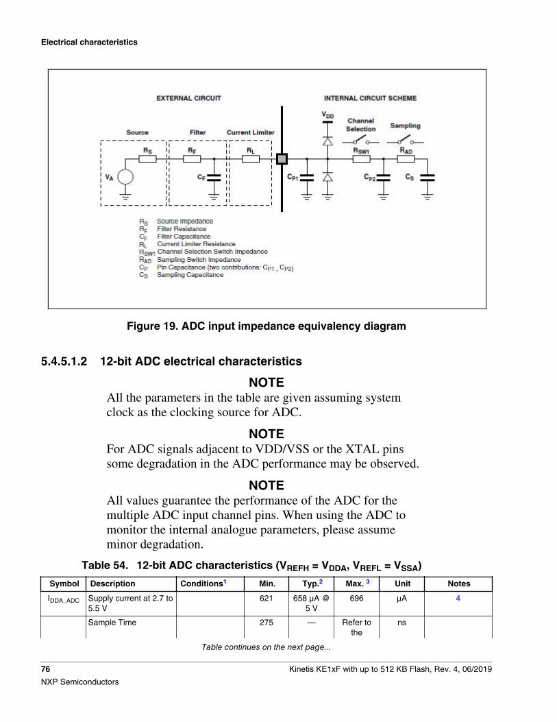
Figure 19. ADC input impedance equivalency diagram
5.4.5.1.2 12-bit ADC electrical characteristics
NOTEAll the parameters in the table are given assuming systemclock as the clocking source for ADC.
NOTEFor ADC signals adjacent to VDD/VSS or the XTAL pinssome degradation in the ADC performance may be observed.
NOTEAll values guarantee the performance of the ADC for themultiple ADC input channel pins. When using the ADC tomonitor the internal analogue parameters, please assumeminor degradation.
Table 54. 12-bit ADC characteristics (VREFH = VDDA, VREFL = VSSA)
Symbol Description Conditions1 Min. Typ.2 Max. 3 Unit Notes
IDDA_ADC Supply current at 2.7 to5.5 V
621 658 μA @5 V
696 μA 4
Sample Time 275 — Refer tothe
ns
Table continues on the next page...
Electrical characteristics
76 Kinetis KE1xF with up to 512 KB Flash, Rev. 4, 06/2019
NXP Semiconductors
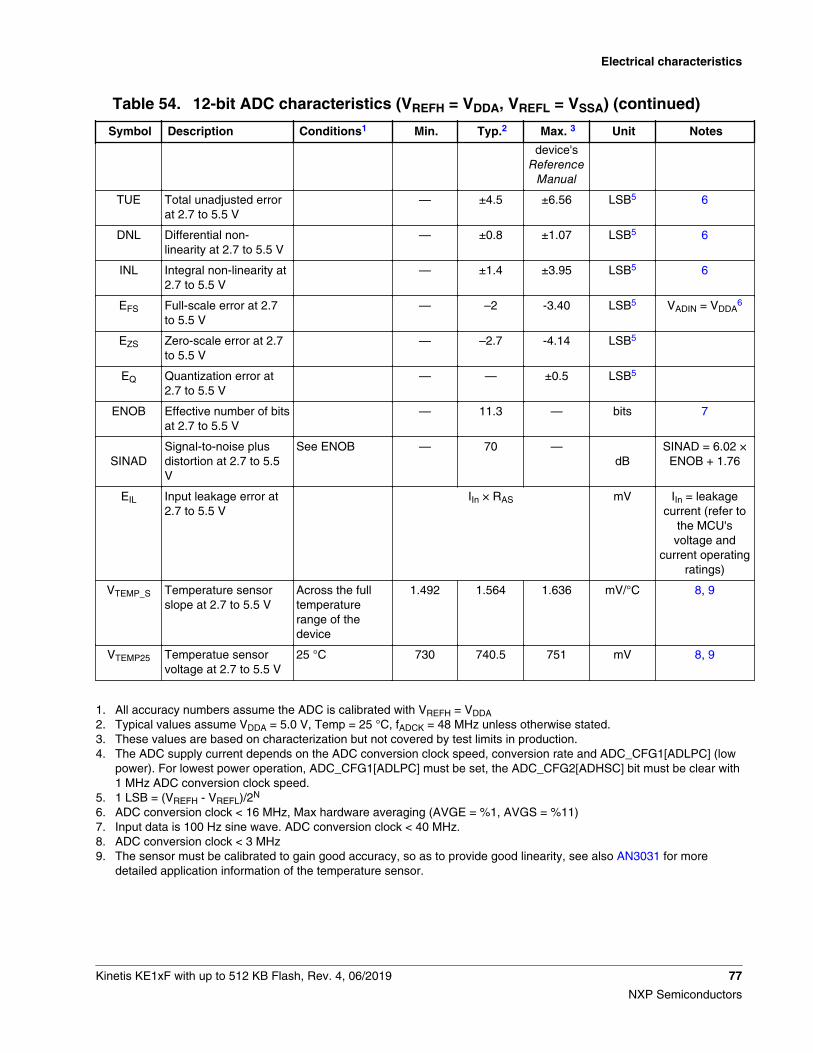
Table 54. 12-bit ADC characteristics (VREFH = VDDA, VREFL = VSSA) (continued)
Symbol Description Conditions1 Min. Typ.2 Max. 3 Unit Notes
device'sReference
Manual
TUE Total unadjusted errorat 2.7 to 5.5 V
— ±4.5 ±6.56 LSB5 6
DNL Differential non-linearity at 2.7 to 5.5 V
— ±0.8 ±1.07 LSB5 6
INL Integral non-linearity at2.7 to 5.5 V
— ±1.4 ±3.95 LSB5 6
EFS Full-scale error at 2.7to 5.5 V
— –2 -3.40 LSB5 VADIN = VDDA6
EZS Zero-scale error at 2.7to 5.5 V
— –2.7 -4.14 LSB5
EQ Quantization error at2.7 to 5.5 V
— — ±0.5 LSB5
ENOB Effective number of bitsat 2.7 to 5.5 V
— 11.3 — bits 7
SINADSignal-to-noise plusdistortion at 2.7 to 5.5V
See ENOB — 70 —dB
SINAD = 6.02 ×ENOB + 1.76
EIL Input leakage error at2.7 to 5.5 V
IIn × RAS mV IIn = leakagecurrent (refer to
the MCU'svoltage and
current operatingratings)
VTEMP_S Temperature sensorslope at 2.7 to 5.5 V
Across the fulltemperaturerange of thedevice
1.492 1.564 1.636 mV/°C 8, 9
VTEMP25 Temperatue sensorvoltage at 2.7 to 5.5 V
25 °C 730 740.5 751 mV 8, 9
1. All accuracy numbers assume the ADC is calibrated with VREFH = VDDA2. Typical values assume VDDA = 5.0 V, Temp = 25 °C, fADCK = 48 MHz unless otherwise stated.3. These values are based on characterization but not covered by test limits in production.4. The ADC supply current depends on the ADC conversion clock speed, conversion rate and ADC_CFG1[ADLPC] (low
power). For lowest power operation, ADC_CFG1[ADLPC] must be set, the ADC_CFG2[ADHSC] bit must be clear with1 MHz ADC conversion clock speed.
5. 1 LSB = (VREFH - VREFL)/2N
6. ADC conversion clock < 16 MHz, Max hardware averaging (AVGE = %1, AVGS = %11)7. Input data is 100 Hz sine wave. ADC conversion clock < 40 MHz.8. ADC conversion clock < 3 MHz9. The sensor must be calibrated to gain good accuracy, so as to provide good linearity, see also AN3031 for more
detailed application information of the temperature sensor.
Electrical characteristics
Kinetis KE1xF with up to 512 KB Flash, Rev. 4, 06/2019 77
NXP Semiconductors
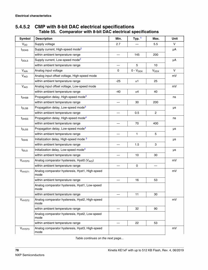
5.4.5.2 CMP with 8-bit DAC electrical specificationsTable 55. Comparator with 8-bit DAC electrical specifications
Symbol Description Min. Typ. 1 Max. Unit
VDD Supply voltage 2.7 — 5.5 V
IDDHS Supply current, High-speed mode2 μA
within ambient temperature range — 145 200
IDDLS Supply current, Low-speed mode2 μA
within ambient temperature range — 5 10
VAIN Analog input voltage 0 0 - VDDX VDDX V
VAIO Analog input offset voltage, High-speed mode mV
within ambient temperature range -25 ±1 25
VAIO Analog input offset voltage, Low-speed mode mV
within ambient temperature range -40 ±4 40
tDHSB Propagation delay, High-speed mode3 ns
within ambient temperature range — 30 200
tDLSB Propagation delay, Low-speed mode3 µs
within ambient temperature range — 0.5 2
tDHSS Propagation delay, High-speed mode4 ns
within ambient temperature range — 70 400
tDLSS Propagation delay, Low-speed mode4 µs
within ambient temperature range — 1 5
tIDHS Initialization delay, High-speed mode 3 μs
within ambient temperature range — 1.5 3
tIDLS Initialization delay, Low-speed mode3 μs
within ambient temperature range — 10 30
VHYST0 Analog comparator hysteresis, Hyst0 (VAIO) mV
within ambient temperature range — 0 —
VHYST1 Analog comparator hysteresis, Hyst1, High-speedmode
mV
within ambient temperature range — 16 53
Analog comparator hysteresis, Hyst1, Low-speedmode
within ambient temperature range — 11 30
VHYST2 Analog comparator hysteresis, Hyst2, High-speedmode
mV
within ambient temperature range — 32 90
Analog comparator hysteresis, Hyst2, Low-speedmode
within ambient temperature range — 22 53
VHYST3 Analog comparator hysteresis, Hyst3, High-speedmode
mV
Table continues on the next page...
Electrical characteristics
78 Kinetis KE1xF with up to 512 KB Flash, Rev. 4, 06/2019
NXP Semiconductors
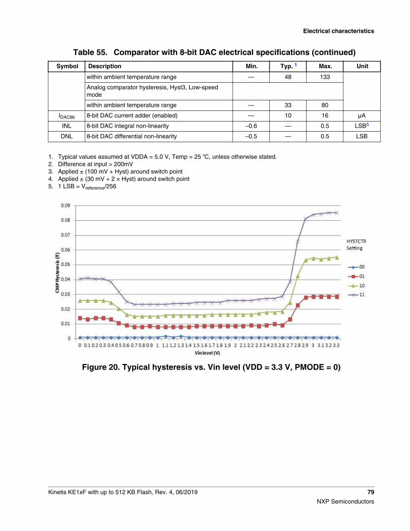
Table 55. Comparator with 8-bit DAC electrical specifications (continued)
Symbol Description Min. Typ. 1 Max. Unit
within ambient temperature range — 48 133
Analog comparator hysteresis, Hyst3, Low-speedmode
within ambient temperature range — 33 80
IDAC8b 8-bit DAC current adder (enabled) — 10 16 μA
INL 8-bit DAC integral non-linearity –0.6 — 0.5 LSB5
DNL 8-bit DAC differential non-linearity –0.5 — 0.5 LSB
1. Typical values assumed at VDDA = 5.0 V, Temp = 25 , unless otherwise stated.2. Difference at input > 200mV3. Applied ± (100 mV + Hyst) around switch point4. Applied ± (30 mV + 2 × Hyst) around switch point5. 1 LSB = Vreference/256
Figure 20. Typical hysteresis vs. Vin level (VDD = 3.3 V, PMODE = 0)
Electrical characteristics
Kinetis KE1xF with up to 512 KB Flash, Rev. 4, 06/2019 79
NXP Semiconductors
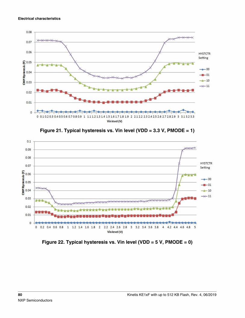
Figure 21. Typical hysteresis vs. Vin level (VDD = 3.3 V, PMODE = 1)
Figure 22. Typical hysteresis vs. Vin level (VDD = 5 V, PMODE = 0)
Electrical characteristics
80 Kinetis KE1xF with up to 512 KB Flash, Rev. 4, 06/2019
NXP Semiconductors
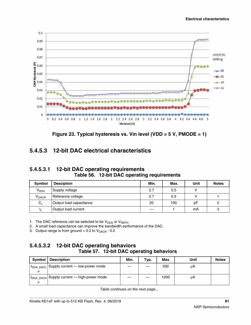
Figure 23. Typical hysteresis vs. Vin level (VDD = 5 V, PMODE = 1)
5.4.5.3 12-bit DAC electrical characteristics
5.4.5.3.1 12-bit DAC operating requirementsTable 56. 12-bit DAC operating requirements
Symbol Desciption Min. Max. Unit Notes
VDDA Supply voltage 2.7 5.5 V
VDACR Reference voltage 2.7 5.5 V 1
CL Output load capacitance 20 100 pF 2
IL Output load current — 1 mA 3
1. The DAC reference can be selected to be VDDA or VREFH.2. A small load capacitance can improve the bandwidth performance of the DAC.3. Output range is from ground + 0.2 to VDACR - 0.2
5.4.5.3.2 12-bit DAC operating behaviorsTable 57. 12-bit DAC operating behaviors
Symbol Description Min. Typ. Max. Unit Notes
IDDA_DACL
P
Supply current — low-power mode — — 330 μA
IDDA_DACH
P
Supply current — high-power mode — — 1200 μA
Table continues on the next page...
Electrical characteristics
Kinetis KE1xF with up to 512 KB Flash, Rev. 4, 06/2019 81
NXP Semiconductors
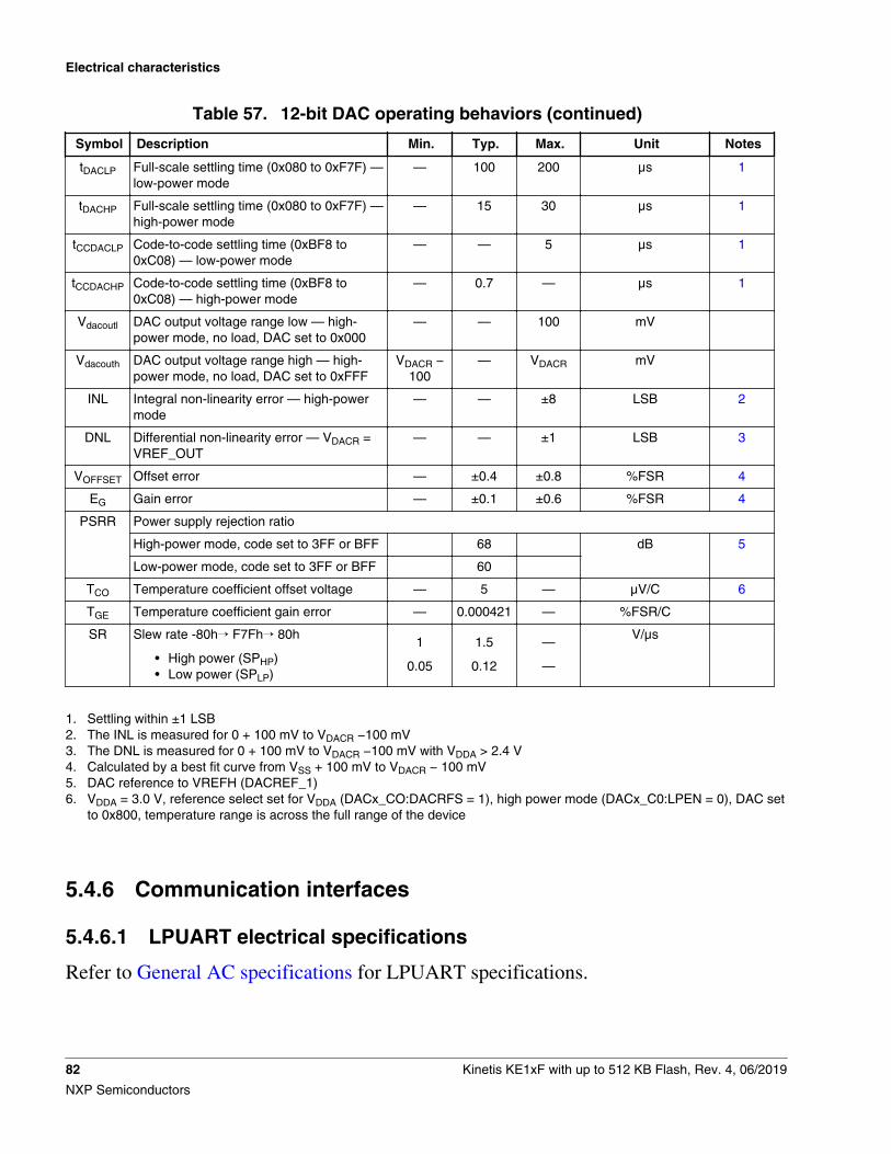
Table 57. 12-bit DAC operating behaviors (continued)
Symbol Description Min. Typ. Max. Unit Notes
tDACLP Full-scale settling time (0x080 to 0xF7F) —low-power mode
— 100 200 μs 1
tDACHP Full-scale settling time (0x080 to 0xF7F) —high-power mode
— 15 30 μs 1
tCCDACLP Code-to-code settling time (0xBF8 to0xC08) — low-power mode
— — 5 μs 1
tCCDACHP Code-to-code settling time (0xBF8 to0xC08) — high-power mode
— 0.7 — μs 1
Vdacoutl DAC output voltage range low — high-power mode, no load, DAC set to 0x000
— — 100 mV
Vdacouth DAC output voltage range high — high-power mode, no load, DAC set to 0xFFF
VDACR −100
— VDACR mV
INL Integral non-linearity error — high-powermode
— — ±8 LSB 2
DNL Differential non-linearity error — VDACR =VREF_OUT
— — ±1 LSB 3
VOFFSET Offset error — ±0.4 ±0.8 %FSR 4
EG Gain error — ±0.1 ±0.6 %FSR 4
PSRR Power supply rejection ratio
High-power mode, code set to 3FF or BFF 68 dB 5
Low-power mode, code set to 3FF or BFF 60
TCO Temperature coefficient offset voltage — 5 — μV/C 6
TGE Temperature coefficient gain error — 0.000421 — %FSR/C
SR Slew rate -80h→ F7Fh→ 80h
• High power (SPHP)• Low power (SPLP)
1
0.05
1.5
0.12
—
—
V/μs
1. Settling within ±1 LSB2. The INL is measured for 0 + 100 mV to VDACR −100 mV3. The DNL is measured for 0 + 100 mV to VDACR −100 mV with VDDA > 2.4 V4. Calculated by a best fit curve from VSS + 100 mV to VDACR − 100 mV5. DAC reference to VREFH (DACREF_1)6. VDDA = 3.0 V, reference select set for VDDA (DACx_CO:DACRFS = 1), high power mode (DACx_C0:LPEN = 0), DAC set
to 0x800, temperature range is across the full range of the device
5.4.6 Communication interfaces
5.4.6.1 LPUART electrical specifications
Refer to General AC specifications for LPUART specifications.
Electrical characteristics
82 Kinetis KE1xF with up to 512 KB Flash, Rev. 4, 06/2019
NXP Semiconductors
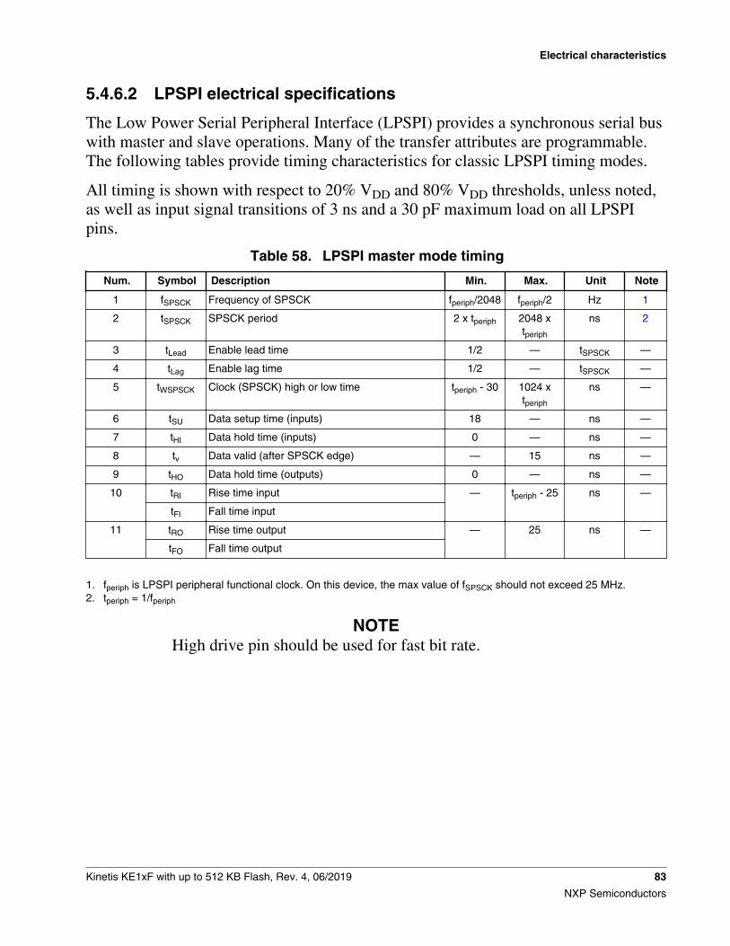
5.4.6.2 LPSPI electrical specifications
The Low Power Serial Peripheral Interface (LPSPI) provides a synchronous serial buswith master and slave operations. Many of the transfer attributes are programmable.The following tables provide timing characteristics for classic LPSPI timing modes.
All timing is shown with respect to 20% VDD and 80% VDD thresholds, unless noted,as well as input signal transitions of 3 ns and a 30 pF maximum load on all LPSPIpins.
Table 58. LPSPI master mode timing
Num. Symbol Description Min. Max. Unit Note
1 fSPSCK Frequency of SPSCK fperiph/2048 fperiph/2 Hz 1
2 tSPSCK SPSCK period 2 x tperiph 2048 xtperiph
ns 2
3 tLead Enable lead time 1/2 — tSPSCK —
4 tLag Enable lag time 1/2 — tSPSCK —
5 tWSPSCK Clock (SPSCK) high or low time tperiph - 30 1024 xtperiph
ns —
6 tSU Data setup time (inputs) 18 — ns —
7 tHI Data hold time (inputs) 0 — ns —
8 tv Data valid (after SPSCK edge) — 15 ns —
9 tHO Data hold time (outputs) 0 — ns —
10 tRI Rise time input — tperiph - 25 ns —
tFI Fall time input
11 tRO Rise time output — 25 ns —
tFO Fall time output
1. fperiph is LPSPI peripheral functional clock. On this device, the max value of fSPSCK should not exceed 25 MHz.2. tperiph = 1/fperiph
NOTEHigh drive pin should be used for fast bit rate.
Electrical characteristics
Kinetis KE1xF with up to 512 KB Flash, Rev. 4, 06/2019 83
NXP Semiconductors
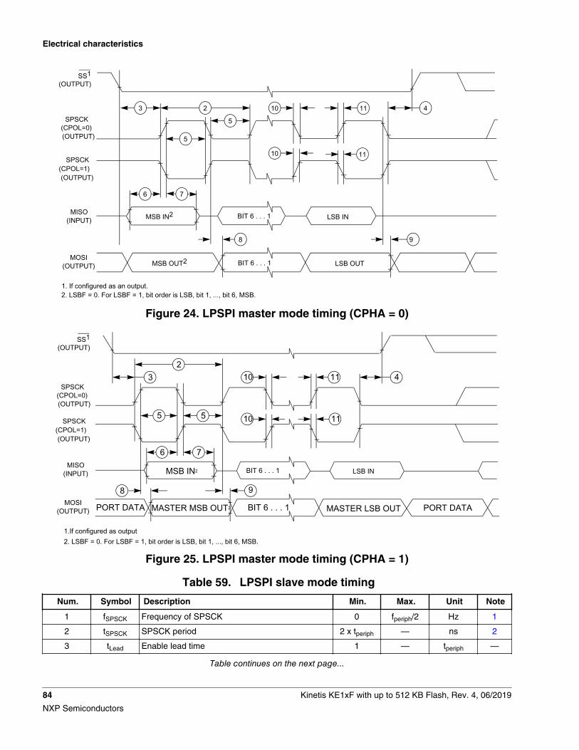
(OUTPUT)
2
8
6 7
MSB IN2 LSB IN
MSB OUT2 LSB OUT
9
5
5
3
(CPOL=0)
411
1110
10SPSCK
SPSCK(CPOL=1)
2. LSBF = 0. For LSBF = 1, bit order is LSB, bit 1, ..., bit 6, MSB.1. If configured as an output.
SS1
(OUTPUT)
(OUTPUT)
MOSI(OUTPUT)
MISO(INPUT) BIT 6 . . . 1
BIT 6 . . . 1
Figure 24. LPSPI master mode timing (CPHA = 0)
<<CLASSIFICATION>> <<NDA MESSAGE>>
38
2
6 7
MSB IN2
BIT 6 . . . 1 MASTER MSB OUT2 MASTER LSB OUT
55
8
10 11
PORT DATA PORT DATA
3 10 11 4
1.If configured as output 2. LSBF = 0. For LSBF = 1, bit order is LSB, bit 1, ..., bit 6, MSB.
9
(OUTPUT)
(CPOL=0)SPSCK
SPSCK(CPOL=1)
SS1
(OUTPUT)
(OUTPUT)
MOSI(OUTPUT)
MISO(INPUT) LSB INBIT 6 . . . 1
Figure 25. LPSPI master mode timing (CPHA = 1)
Table 59. LPSPI slave mode timing
Num. Symbol Description Min. Max. Unit Note
1 fSPSCK Frequency of SPSCK 0 fperiph/2 Hz 1
2 tSPSCK SPSCK period 2 x tperiph — ns 2
3 tLead Enable lead time 1 — tperiph —
Table continues on the next page...
Electrical characteristics
84 Kinetis KE1xF with up to 512 KB Flash, Rev. 4, 06/2019
NXP Semiconductors
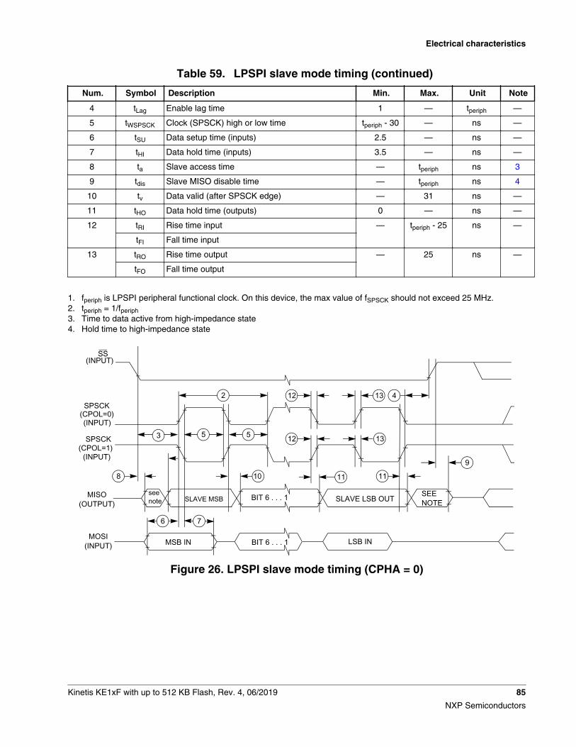
Table 59. LPSPI slave mode timing (continued)
Num. Symbol Description Min. Max. Unit Note
4 tLag Enable lag time 1 — tperiph —
5 tWSPSCK Clock (SPSCK) high or low time tperiph - 30 — ns —
6 tSU Data setup time (inputs) 2.5 — ns —
7 tHI Data hold time (inputs) 3.5 — ns —
8 ta Slave access time — tperiph ns 3
9 tdis Slave MISO disable time — tperiph ns 4
10 tv Data valid (after SPSCK edge) — 31 ns —
11 tHO Data hold time (outputs) 0 — ns —
12 tRI Rise time input — tperiph - 25 ns —
tFI Fall time input
13 tRO Rise time output — 25 ns —
tFO Fall time output
1. fperiph is LPSPI peripheral functional clock. On this device, the max value of fSPSCK should not exceed 25 MHz.2. tperiph = 1/fperiph3. Time to data active from high-impedance state4. Hold time to high-impedance state
2
10
6 7
MSB IN
BIT 6 . . . 1 SLAVE MSB SLAVE LSB OUT
11
553
8
4
13
12
12
11
SEE NOTE
13
9
see note
(INPUT)
(CPOL=0)SPSCK
SPSCK(CPOL=1)
SS
(INPUT)
(INPUT)
MOSI(INPUT)
MISO(OUTPUT)
LSB INBIT 6 . . . 1
Figure 26. LPSPI slave mode timing (CPHA = 0)
Electrical characteristics
Kinetis KE1xF with up to 512 KB Flash, Rev. 4, 06/2019 85
NXP Semiconductors
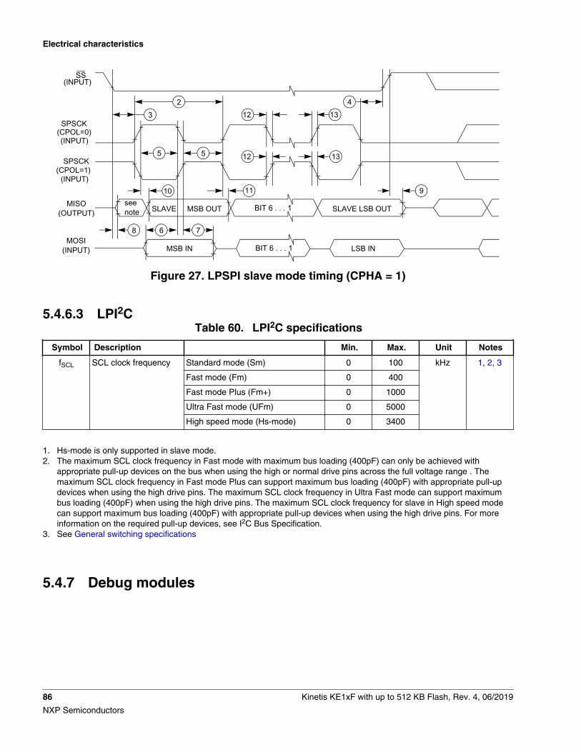
2
6 7
MSB IN
BIT 6 . . . 1 MSB OUT SLAVE LSB OUT
55
10
12 13
3 12 134
SLAVE
8
9see note
(INPUT)
(CPOL=0)SPSCK
SPSCK(CPOL=1)
SS
(INPUT)
(INPUT)
MOSI(INPUT)
MISO(OUTPUT)
11
LSB INBIT 6 . . . 1
Figure 27. LPSPI slave mode timing (CPHA = 1)
5.4.6.3 LPI2CTable 60. LPI2C specifications
Symbol Description Min. Max. Unit Notes
fSCL SCL clock frequency Standard mode (Sm) 0 100 kHz 1, 2, 3
Fast mode (Fm) 0 400
Fast mode Plus (Fm+) 0 1000
Ultra Fast mode (UFm) 0 5000
High speed mode (Hs-mode) 0 3400
1. Hs-mode is only supported in slave mode.2. The maximum SCL clock frequency in Fast mode with maximum bus loading (400pF) can only be achieved with
appropriate pull-up devices on the bus when using the high or normal drive pins across the full voltage range . Themaximum SCL clock frequency in Fast mode Plus can support maximum bus loading (400pF) with appropriate pull-updevices when using the high drive pins. The maximum SCL clock frequency in Ultra Fast mode can support maximumbus loading (400pF) when using the high drive pins. The maximum SCL clock frequency for slave in High speed modecan support maximum bus loading (400pF) with appropriate pull-up devices when using the high drive pins. For moreinformation on the required pull-up devices, see I2C Bus Specification.
3. See General switching specifications
5.4.7 Debug modules
Electrical characteristics
86 Kinetis KE1xF with up to 512 KB Flash, Rev. 4, 06/2019
NXP Semiconductors
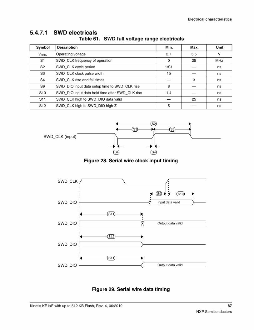
5.4.7.1 SWD electricalsTable 61. SWD full voltage range electricals
Symbol Description Min. Max. Unit
VDDA Operating voltage 2.7 5.5 V
S1 SWD_CLK frequency of operation 0 25 MHz
S2 SWD_CLK cycle period 1/S1 — ns
S3 SWD_CLK clock pulse width 15 — ns
S4 SWD_CLK rise and fall times — 3 ns
S9 SWD_DIO input data setup time to SWD_CLK rise 8 — ns
S10 SWD_DIO input data hold time after SWD_CLK rise 1.4 — ns
S11 SWD_CLK high to SWD_DIO data valid — 25 ns
S12 SWD_CLK high to SWD_DIO high-Z 5 — ns
S2S3 S3
S4 S4
SWD_CLK (input)
Figure 28. Serial wire clock input timing
S11
S12
S11
S9 S10
Input data valid
Output data valid
Output data valid
SWD_CLK
SWD_DIO
SWD_DIO
SWD_DIO
SWD_DIO
Figure 29. Serial wire data timing
Electrical characteristics
Kinetis KE1xF with up to 512 KB Flash, Rev. 4, 06/2019 87
NXP Semiconductors
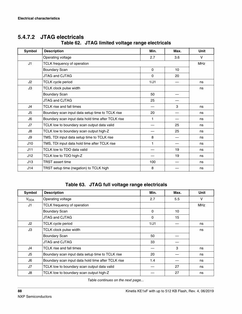
5.4.7.2 JTAG electricalsTable 62. JTAG limited voltage range electricals
Symbol Description Min. Max. Unit
Operating voltage 2.7 3.6 V
J1 TCLK frequency of operation MHz
Boundary Scan 0 10
JTAG and CJTAG 0 20
J2 TCLK cycle period 1/J1 — ns
J3 TCLK clock pulse width ns
Boundary Scan 50 —
JTAG and CJTAG 25 —
J4 TCLK rise and fall times — 3 ns
J5 Boundary scan input data setup time to TCLK rise 20 — ns
J6 Boundary scan input data hold time after TCLK rise 1 — ns
J7 TCLK low to boundary scan output data valid — 25 ns
J8 TCLK low to boundary scan output high-Z — 25 ns
J9 TMS, TDI input data setup time to TCLK rise 8 — ns
J10 TMS, TDI input data hold time after TCLK rise 1 — ns
J11 TCLK low to TDO data valid — 19 ns
J12 TCLK low to TDO high-Z — 19 ns
J13 TRST assert time 100 — ns
J14 TRST setup time (negation) to TCLK high 8 — ns
Table 63. JTAG full voltage range electricals
Symbol Description Min. Max. Unit
VDDA Operating voltage 2.7 5.5 V
J1 TCLK frequency of operation MHz
Boundary Scan 0 10
JTAG and CJTAG 0 15
J2 TCLK cycle period 1/J1 — ns
J3 TCLK clock pulse width ns
Boundary Scan 50 —
JTAG and CJTAG 33 —
J4 TCLK rise and fall times — 3 ns
J5 Boundary scan input data setup time to TCLK rise 20 — ns
J6 Boundary scan input data hold time after TCLK rise 1.4 — ns
J7 TCLK low to boundary scan output data valid — 27 ns
J8 TCLK low to boundary scan output high-Z — 27 ns
Table continues on the next page...
Electrical characteristics
88 Kinetis KE1xF with up to 512 KB Flash, Rev. 4, 06/2019
NXP Semiconductors
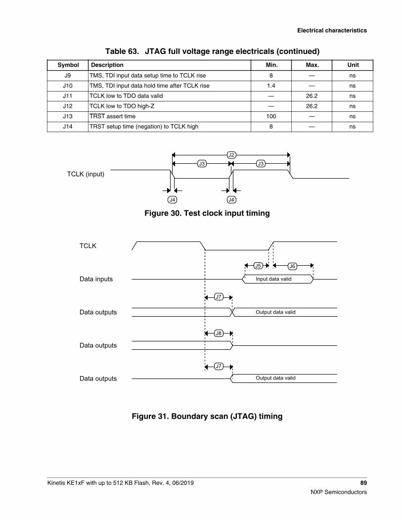
Table 63. JTAG full voltage range electricals (continued)
Symbol Description Min. Max. Unit
J9 TMS, TDI input data setup time to TCLK rise 8 — ns
J10 TMS, TDI input data hold time after TCLK rise 1.4 — ns
J11 TCLK low to TDO data valid — 26.2 ns
J12 TCLK low to TDO high-Z — 26.2 ns
J13 TRST assert time 100 — ns
J14 TRST setup time (negation) to TCLK high 8 — ns
J2J3 J3
J4 J4
TCLK (input)
Figure 30. Test clock input timing
J7
J8
J7
J5 J6
Input data valid
Output data valid
Output data valid
TCLK
Data inputs
Data outputs
Data outputs
Data outputs
Figure 31. Boundary scan (JTAG) timing
Electrical characteristics
Kinetis KE1xF with up to 512 KB Flash, Rev. 4, 06/2019 89
NXP Semiconductors
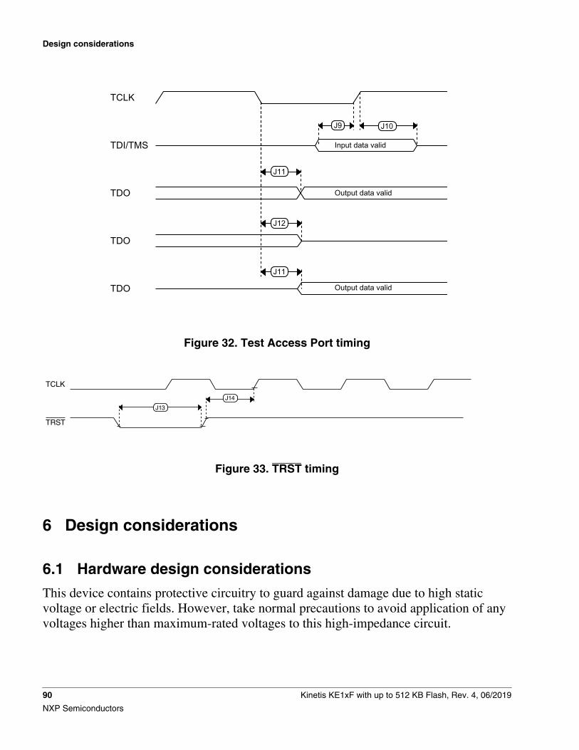
J11
J12
J11
J9 J10
Input data valid
Output data valid
Output data valid
TCLK
TDI/TMS
TDO
TDO
TDO
Figure 32. Test Access Port timing
J14
J13
TCLK
TRST
Figure 33. TRST timing
6 Design considerations
6.1 Hardware design considerations
This device contains protective circuitry to guard against damage due to high staticvoltage or electric fields. However, take normal precautions to avoid application of anyvoltages higher than maximum-rated voltages to this high-impedance circuit.
Design considerations
90 Kinetis KE1xF with up to 512 KB Flash, Rev. 4, 06/2019
NXP Semiconductors
6.1.1 Printed circuit board recommendations• Place connectors or cables on one edge of the board and do not place digital
circuits between connectors.• Drivers and filters for I/O functions must be placed as close to the connectors as
possible. Connect TVS devices at the connector to a good ground. Connect filtercapacitors at the connector to a good ground. Consider to add ferrite bead orinductor to some sensitive lines.
• Physically isolate analog circuits from digital circuits if possible.• Place input filter capacitors as close to the MCU as possible.• For best EMC performance, route signals as transmission lines; use a ground
plane directly under LQFP packages; and solder the exposed pad (EP) to grounddirectly under QFN packages.
6.1.2 Power delivery systemConsider the following items in the power delivery system:
• Use a plane for ground.• Use a plane for MCU VDD supply if possible.• Always route ground first, as a plane or continuous surface, and never as
sequential segments.• Always route the power net as star topology, and make each power trace loop as
minimum as possible.• Route power next, as a plane or traces that are parallel to ground traces.• Place bulk capacitance, 10 μF or more, at the entrance of the power plane.• Place bypass capacitors for MCU power domain as close as possible to each
VDD/VSS pair, including VDDA/VSSA and VREFH/VREFL.• The minimum bypass requirement is to place 0.1 μF capacitors positioned as near
as possible to the package supply pins.
6.1.3 Analog design
Each ADC input must have an RC filter as shown in the following figure. Themaximum value of R must be RAS max if fast sampling and high resolution arerequired. The value of C must be chosen to ensure that the RC time constant is verysmall compared to the sample period.
Design considerations
Kinetis KE1xF with up to 512 KB Flash, Rev. 4, 06/2019 91
NXP Semiconductors
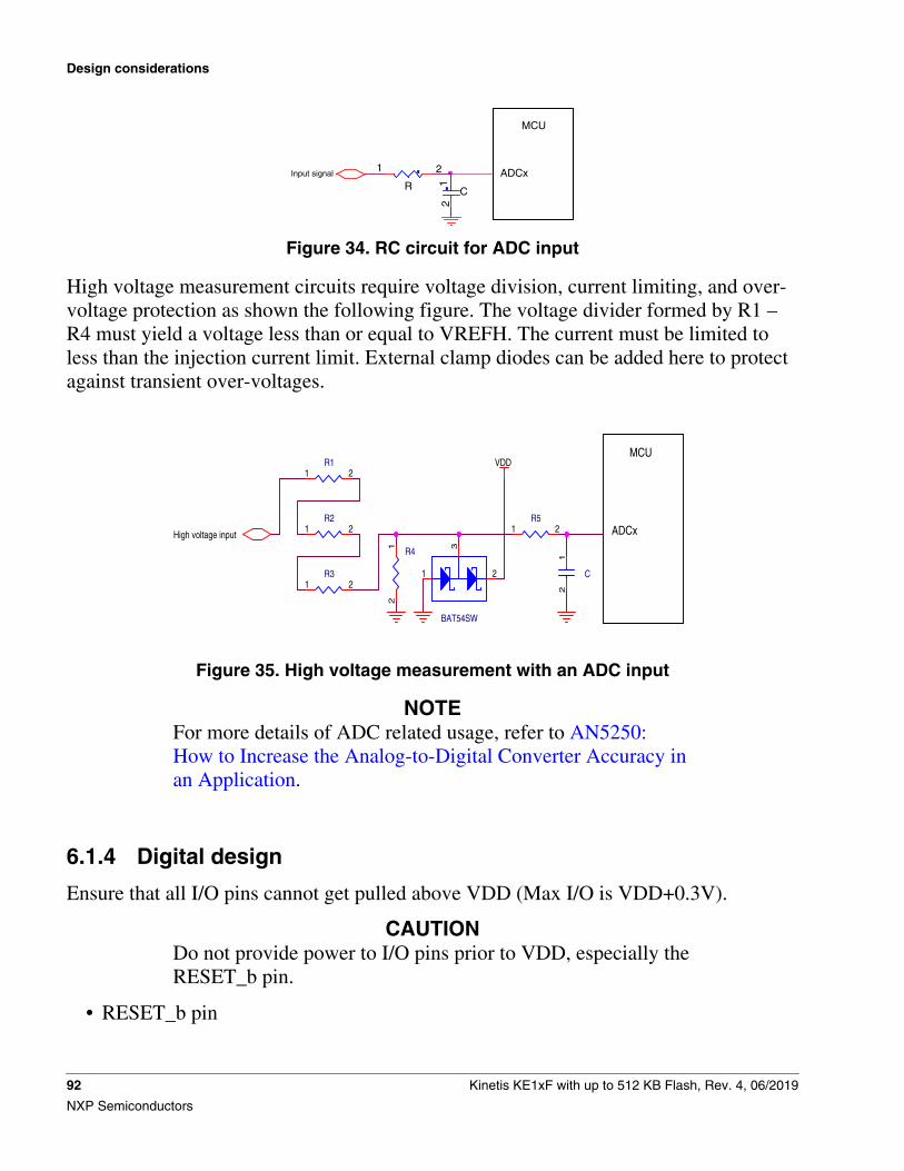
MCU
ADCx
CRInput signal
1 2
12
Figure 34. RC circuit for ADC input
High voltage measurement circuits require voltage division, current limiting, and over-voltage protection as shown the following figure. The voltage divider formed by R1 –R4 must yield a voltage less than or equal to VREFH. The current must be limited toless than the injection current limit. External clamp diodes can be added here to protectagainst transient over-voltages.
5
5
4
4
3
3
2
2
1
1
D D
C C
B B
A A
EXTAL XTAL
OSCILLATOR
EXTAL XTAL
OSCILLATOR
EXTAL XTAL
OSCILLATOR
EXTAL XTAL
OSCILLATOR
EXTAL XTAL
OSCILLATOR
EXTAL XTAL
OSCILLATOR
MCU
ADCx
MCU
ADCx
MCU
RESET_b
MCU
NMI_b
MCU
RESET_b
Supervisor Chip
OUT
Active high,open drain
RESET_b
SWD_DIOSWD_CLK
Analog input
High voltage input
RESET_b
VDD
VDD
VDD
VDD
VDD
VDD
Drawing Title:
Size Document Number Rev
Date: Sheet of
Page Title:
ICAP Classification: FCP: FIUO: PUBI:
SCH-XXXXX PDF: SPF-XXXXX X
<Title>
C
Friday, February 06, 2015
<PageTitle>
1 1
___ ___XDrawing Title:
Size Document Number Rev
Date: Sheet of
Page Title:
ICAP Classification: FCP: FIUO: PUBI:
SCH-XXXXX PDF: SPF-XXXXX X
<Title>
C
Friday, February 06, 2015
<PageTitle>
1 1
___ ___XDrawing Title:
Size Document Number Rev
Date: Sheet of
Page Title:
ICAP Classification: FCP: FIUO: PUBI:
SCH-XXXXX PDF: SPF-XXXXX X
<Title>
C
Friday, February 06, 2015
<PageTitle>
1 1
___ ___X
R
1 2
0.1uF
12
R51 2
Cx
12
0.1uF
12
RESONATOR
1 3
2Cy
12
Cx
12
CRYSTAL
21
J1
HDR_5X2
1 23 4
657 89 10
Cy
12
10k
12
10k
12
R412
CRYSTAL
21
0.1uF
12
10k
12
CRYSTAL
21
R11 2
R31 2
C
12
RESONATOR
1 3
2
R21 2
10k
12
10k
12
RF
1 2
RS
12
BAT54SW
1 2
3
RS
12
RS
12
C1
2
RF
1 2
RS
1 2
RF
1 2
CRYSTAL
21
Figure 35. High voltage measurement with an ADC input
NOTEFor more details of ADC related usage, refer to AN5250:How to Increase the Analog-to-Digital Converter Accuracy inan Application.
6.1.4 Digital design
Ensure that all I/O pins cannot get pulled above VDD (Max I/O is VDD+0.3V).
CAUTIONDo not provide power to I/O pins prior to VDD, especially theRESET_b pin.
• RESET_b pin
Design considerations
92 Kinetis KE1xF with up to 512 KB Flash, Rev. 4, 06/2019
NXP Semiconductors
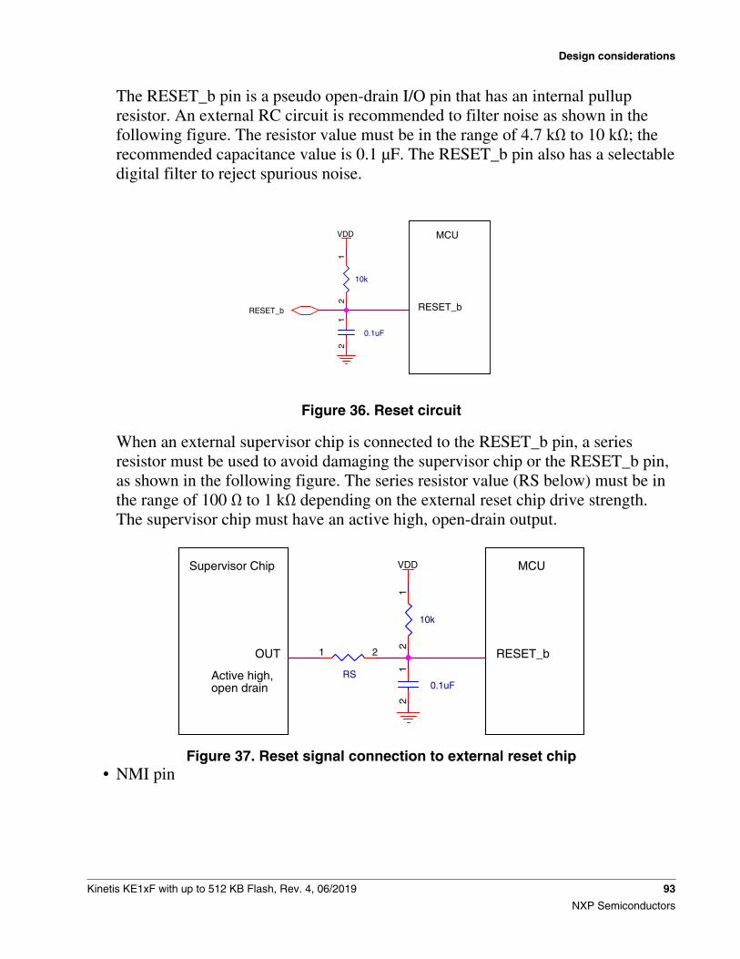
The RESET_b pin is a pseudo open-drain I/O pin that has an internal pullupresistor. An external RC circuit is recommended to filter noise as shown in thefollowing figure. The resistor value must be in the range of 4.7 kΩ to 10 kΩ; therecommended capacitance value is 0.1 μF. The RESET_b pin also has a selectabledigital filter to reject spurious noise.
5
5
4
4
3
3
2
2
1
1
D D
C C
B B
A A
EXTAL XTAL OSCILLATOR
EXTAL XTAL OSCILLATOR
EXTAL XTAL OSCILLATOR EXTAL XTAL OSCILLATOR
EXTAL XTAL OSCILLATOR EXTAL XTAL OSCILLATOR
MCU
ADCx
MCU
ADCx
MCU
RESET_b
MCU
NMI_b
MCU
RESET_b
Supervisor Chip
OUT Active high, open drain
RESET_b
SWD_DIOSWD_CLK
Analog input
High voltage input
RESET_b
VDD
VDD
VDD
VDD
VDD
VDD
Drawing Title: Size Document Number Rev Date: Sheet of Page Title:
ICAP Classification: FCP: FIUO: PUBI:
SCH-XXXXX PDF: SPF-XXXXX X
<Title>
C Friday, February 06, 2015
<PageTitle>
1 1
___ ___ X Drawing Title: Size Document Number Rev Date: Sheet of Page Title:
ICAP Classification: FCP: FIUO: PUBI:
SCH-XXXXX PDF: SPF-XXXXX X
<Title>
C Friday, February 06, 2015
<PageTitle>
1 1
___ ___ X Drawing Title: Size Document Number Rev Date: Sheet of Page Title:
ICAP Classification: FCP: FIUO: PUBI:
SCH-XXXXX PDF: SPF-XXXXX X
<Title>
C Friday, February 06, 2015
<PageTitle>
1 1
___ ___ X
R
1 2
0.1uF1
2
R51 2
Cx
12
0.1uF
12
RESONATOR
1 3
2Cy
12
Cx
12
CRYSTAL
21
J1
HDR_5X2
1 23 4
657 89 10
Cy
12
10k
12
10k
12
R412
CRYSTAL
21
0.1uF
12
10k
12
CRYSTAL
21
R11 2
R31 2
C
12
RESONATOR
1 3
2
R21 2
10k
12
10k
12
RF
1 2
RS
12
BAT54SW
1 2
3
RS
12
RS
12
C
12
RF
1 2
RS
1 2
RF
1 2
CRYSTAL
21
Figure 36. Reset circuit
When an external supervisor chip is connected to the RESET_b pin, a seriesresistor must be used to avoid damaging the supervisor chip or the RESET_b pin,as shown in the following figure. The series resistor value (RS below) must be inthe range of 100 Ω to 1 kΩ depending on the external reset chip drive strength.The supervisor chip must have an active high, open-drain output.
5
5
4
4
3
3
2
2
1
1
D D
C C
B B
A A
EXTAL XTAL OSCILLATOR
EXTAL XTAL OSCILLATOR
EXTAL XTAL OSCILLATOR EXTAL XTAL OSCILLATOR
EXTAL XTAL OSCILLATOR EXTAL XTAL OSCILLATOR
MCU
ADCx
MCU
ADCx
MCU
RESET_b
MCU
NMI_b
MCU
RESET_b
Supervisor Chip
OUT Active high, open drain
RESET_b
SWD_DIOSWD_CLK
Analog input
High voltage input
RESET_b
VDD
VDD
VDD
VDD
VDD
VDD
Drawing Title: Size Document Number Rev Date: Sheet of Page Title:
ICAP Classification: FCP: FIUO: PUBI:
SCH-XXXXX PDF: SPF-XXXXX X
<Title>
C Friday, February 06, 2015
<PageTitle>
1 1
___ ___ X Drawing Title: Size Document Number Rev Date: Sheet of Page Title:
ICAP Classification: FCP: FIUO: PUBI:
SCH-XXXXX PDF: SPF-XXXXX X
<Title>
C Friday, February 06, 2015
<PageTitle>
1 1
___ ___ X Drawing Title: Size Document Number Rev Date: Sheet of Page Title:
ICAP Classification: FCP: FIUO: PUBI:
SCH-XXXXX PDF: SPF-XXXXX X
<Title>
C Friday, February 06, 2015
<PageTitle>
1 1
___ ___ X
R
1 2
0.1uF
12
R51 2
Cx
12
0.1uF
12
RESONATOR
1 3
2Cy
12
Cx
12
CRYSTAL
21
J1
HDR_5X2
1 23 4
657 89 10
Cy
12
10k
12
10k
12
R412
CRYSTAL
21
0.1uF
12
10k
12
CRYSTAL
21
R11 2
R31 2
C
12
RESONATOR
1 3
2
R21 2
10k
12
10k
12
RF
1 2
RS
12
BAT54SW
1 23
RS
12
RS
12
C
12
RF
1 2
RS
1 2
RF
1 2
CRYSTAL
21
Figure 37. Reset signal connection to external reset chip• NMI pin
Design considerations
Kinetis KE1xF with up to 512 KB Flash, Rev. 4, 06/2019 93
NXP Semiconductors
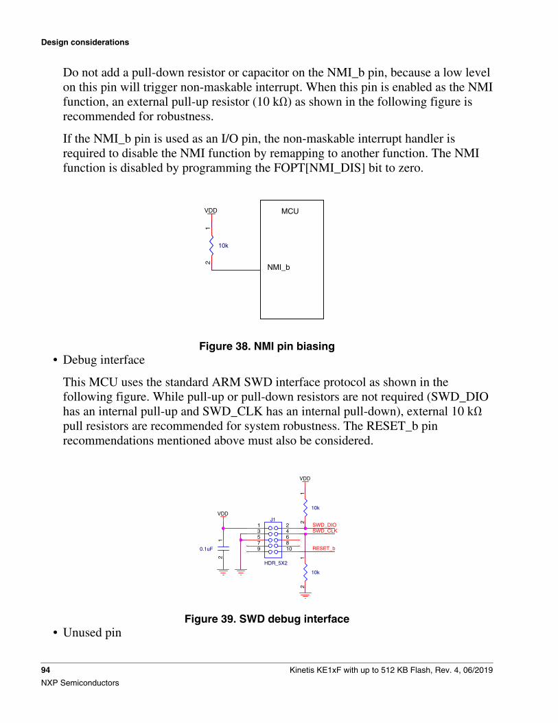
Do not add a pull-down resistor or capacitor on the NMI_b pin, because a low levelon this pin will trigger non-maskable interrupt. When this pin is enabled as the NMIfunction, an external pull-up resistor (10 kΩ) as shown in the following figure isrecommended for robustness.
If the NMI_b pin is used as an I/O pin, the non-maskable interrupt handler isrequired to disable the NMI function by remapping to another function. The NMIfunction is disabled by programming the FOPT[NMI_DIS] bit to zero.
5
5
4
4
3
3
2
2
1
1
D D
C C
B B
A A
EXTAL XTAL OSCILLATOR
EXTAL XTAL OSCILLATOR
EXTAL XTAL OSCILLATOR EXTAL XTAL OSCILLATOR
EXTAL XTAL OSCILLATOR EXTAL XTAL OSCILLATOR
MCU
ADCx
MCU
ADCx
MCU
RESET_b
MCU
NMI_b
MCU
RESET_b
Supervisor Chip
OUT Active high, open drain
RESET_b
SWD_DIOSWD_CLK
Analog input
High voltage input
RESET_b
VDD
VDD
VDD
VDD
VDD
VDD
Drawing Title: Size Document Number Rev Date: Sheet of Page Title:
ICAP Classification: FCP: FIUO: PUBI:
SCH-XXXXX PDF: SPF-XXXXX X
<Title>
C Friday, February 06, 2015
<PageTitle>
1 1
___ ___ X Drawing Title: Size Document Number Rev Date: Sheet of Page Title:
ICAP Classification: FCP: FIUO: PUBI:
SCH-XXXXX PDF: SPF-XXXXX X
<Title>
C Friday, February 06, 2015
<PageTitle>
1 1
___ ___ X Drawing Title: Size Document Number Rev Date: Sheet of Page Title:
ICAP Classification: FCP: FIUO: PUBI:
SCH-XXXXX PDF: SPF-XXXXX X
<Title>
C Friday, February 06, 2015
<PageTitle>
1 1
___ ___ X
R
1 2
0.1uF
12
R51 2
Cx
12
0.1uF
12
RESONATOR
1 3
2Cy
12
Cx
12
CRYSTAL
21
J1
HDR_5X2
1 23 4
657 89 10
Cy
12
10k
12
10k
12
R412
CRYSTAL
21
0.1uF
12
10k
12
CRYSTAL
21
R11 2
R31 2
C
12
RESONATOR
1 3
2
R21 2
10k
12
10k
12
RF
1 2
RS
12
BAT54SW
1 2
3
RS
12
RS
12
C
12
RF
1 2
RS
1 2
RF
1 2
CRYSTAL
21
Figure 38. NMI pin biasing• Debug interface
This MCU uses the standard ARM SWD interface protocol as shown in thefollowing figure. While pull-up or pull-down resistors are not required (SWD_DIOhas an internal pull-up and SWD_CLK has an internal pull-down), external 10 kΩpull resistors are recommended for system robustness. The RESET_b pinrecommendations mentioned above must also be considered.
5
5
4
4
3
3
2
2
1
1
D D
C C
B B
A A
EXTAL XTAL OSCILLATOR
EXTAL XTAL OSCILLATOR
EXTAL XTAL OSCILLATOR EXTAL XTAL OSCILLATOR
EXTAL XTAL OSCILLATOR EXTAL XTAL OSCILLATOR
MCU
ADCx
MCU
ADCx
MCU
RESET_b
MCU
NMI_b
MCU
RESET_b
Supervisor Chip
OUT Active high, open drain
RESET_b
SWD_DIOSWD_CLK
Analog input
High voltage input
RESET_b
VDD
VDD
VDD
VDD
VDD
VDD
Drawing Title: Size Document Number Rev Date: Sheet of Page Title:
ICAP Classification: FCP: FIUO: PUBI:
SCH-XXXXX PDF: SPF-XXXXX X
<Title>
C Friday, February 06, 2015
<PageTitle>
1 1
___ ___ X Drawing Title: Size Document Number Rev Date: Sheet of Page Title:
ICAP Classification: FCP: FIUO: PUBI:
SCH-XXXXX PDF: SPF-XXXXX X
<Title>
C Friday, February 06, 2015
<PageTitle>
1 1
___ ___ X Drawing Title: Size Document Number Rev Date: Sheet of Page Title:
ICAP Classification: FCP: FIUO: PUBI:
SCH-XXXXX PDF: SPF-XXXXX X
<Title>
C Friday, February 06, 2015
<PageTitle>
1 1
___ ___ X
R
1 2
0.1uF
12
R51 2
Cx
12
0.1uF
12
RESONATOR
1 3
2Cy
12
Cx
12
CRYSTAL
21
J1
HDR_5X2
1 23 4
657 89 10
Cy
12
10k
12
10k
12
R412
CRYSTAL
21
0.1uF
12
10k
12
CRYSTAL
21
R11 2
R31 2
C
12
RESONATOR
1 3
2
R21 2
10k
12
10k
12
RF
1 2
RS
12
BAT54SW
1 2
3
RS
12
RS
12
C
12
RF
1 2
RS
1 2
RF
1 2
CRYSTAL
21
Figure 39. SWD debug interface• Unused pin
Design considerations
94 Kinetis KE1xF with up to 512 KB Flash, Rev. 4, 06/2019
NXP Semiconductors
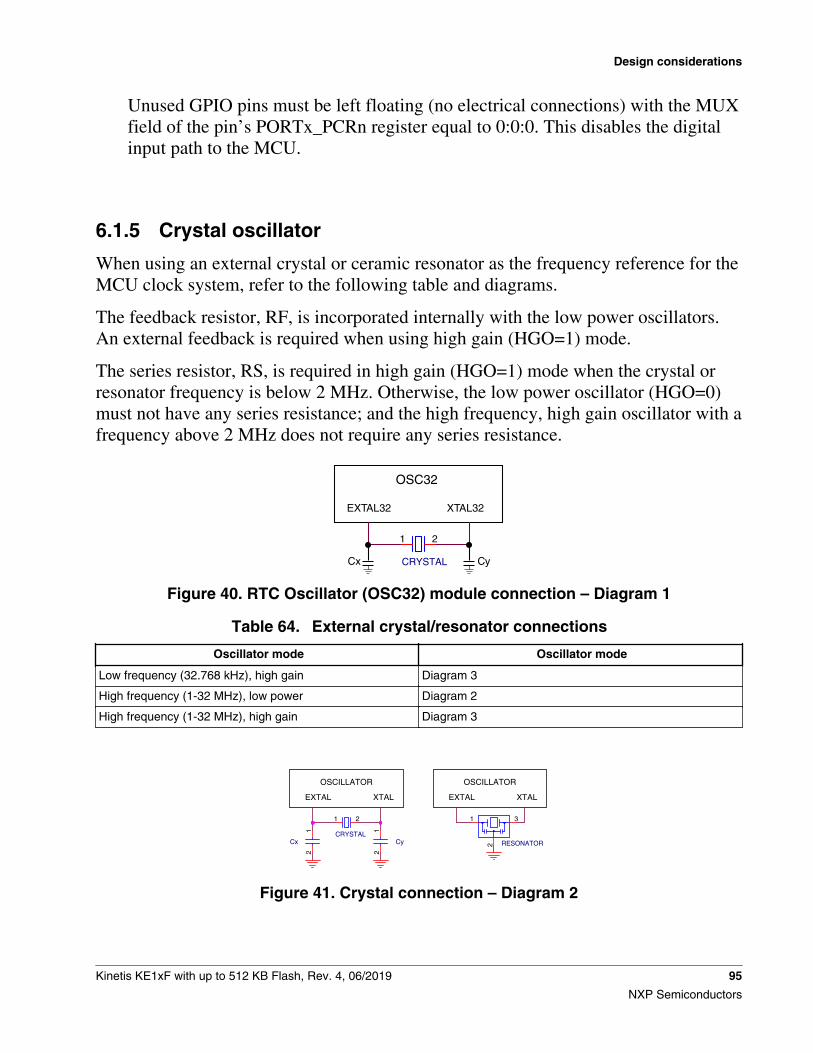
Unused GPIO pins must be left floating (no electrical connections) with the MUXfield of the pin’s PORTx_PCRn register equal to 0:0:0. This disables the digitalinput path to the MCU.
6.1.5 Crystal oscillator
When using an external crystal or ceramic resonator as the frequency reference for theMCU clock system, refer to the following table and diagrams.
The feedback resistor, RF, is incorporated internally with the low power oscillators.An external feedback is required when using high gain (HGO=1) mode.
The series resistor, RS, is required in high gain (HGO=1) mode when the crystal orresonator frequency is below 2 MHz. Otherwise, the low power oscillator (HGO=0)must not have any series resistance; and the high frequency, high gain oscillator with afrequency above 2 MHz does not require any series resistance.
5
5
4
4
3
3
2
2
1
1
D D
C C
B B
A A
Cx Cy
RESET_b
SWD_DIOSWD_CLK
Analog input
High voltage input
RESET_b
VDD
VDD
VDD
VDD
VDD
VDD
Drawing Title: Size Document Number Rev Date: Sheet of Page Title:
ICAP Classification: FCP: FIUO: PUBI:
SCH-XXXXX PDF: SPF-XXXXX X
<Title>
C Friday, February 06, 2015
<PageTitle>
1 1
___ ___ X Drawing Title: Size Document Number Rev Date: Sheet of Page Title:
ICAP Classification: FCP: FIUO: PUBI:
SCH-XXXXX PDF: SPF-XXXXX X
<Title>
C Friday, February 06, 2015
<PageTitle>
1 1
___ ___ X Drawing Title: Size Document Number Rev Date: Sheet of Page Title:
ICAP Classification: FCP: FIUO: PUBI:
SCH-XXXXX PDF: SPF-XXXXX X
<Title>
C Friday, February 06, 2015
<PageTitle>
1 1
___ ___ X
R
1 2
0.1uF
12
R51 2
Cx1
2
0.1uF
12
RESONATOR
1 3
2Cy
12
Cx
12
CRYSTAL
21
J1
HDR_5X2
1 23 4
657 89 10
Cy
12
10k
12
10k
12
R412
CRYSTAL
21
0.1uF
12
10k
12
CRYSTAL
21
R11 2
R31 2
C
12
RESONATOR
1 3
2
R21 2
10k
12
10k
12
RF
1 2
RS
12
BAT54SW
1 2
3
RS
12
RS
12
C
12
RF
1 2
RS
1 2
RF
1 2
CRYSTAL
21
EXTAL32 XTAL32
OSC32
Figure 40. RTC Oscillator (OSC32) module connection – Diagram 1
Table 64. External crystal/resonator connections
Oscillator mode Oscillator mode
Low frequency (32.768 kHz), high gain Diagram 3
High frequency (1-32 MHz), low power Diagram 2
High frequency (1-32 MHz), high gain Diagram 3
5
5
4
4
3
3
2
2
1
1
D D
C C
B B
A A
EXTAL XTAL OSCILLATOR
EXTAL XTAL OSCILLATOR
EXTAL XTAL OSCILLATOR EXTAL XTAL OSCILLATOR
EXTAL XTAL OSCILLATOR EXTAL XTAL OSCILLATOR
MCU
ADCx
MCU
ADCx
MCU
RESET_b
MCU
NMI_b
MCU
RESET_b
Supervisor Chip
OUT Active high, open drain
RESET_b
SWD_DIOSWD_CLK
Analog input
High voltage input
RESET_b
VDD
VDD
VDD
VDD
VDD
VDD
Drawing Title: Size Document Number Rev Date: Sheet of Page Title:
ICAP Classification: FCP: FIUO: PUBI:
SCH-XXXXX PDF: SPF-XXXXX X
<Title>
C Friday, February 06, 2015
<PageTitle>
1 1
___ ___ X Drawing Title: Size Document Number Rev Date: Sheet of Page Title:
ICAP Classification: FCP: FIUO: PUBI:
SCH-XXXXX PDF: SPF-XXXXX X
<Title>
C Friday, February 06, 2015
<PageTitle>
1 1
___ ___ X Drawing Title: Size Document Number Rev Date: Sheet of Page Title:
ICAP Classification: FCP: FIUO: PUBI:
SCH-XXXXX PDF: SPF-XXXXX X
<Title>
C Friday, February 06, 2015
<PageTitle>
1 1
___ ___ X
R
1 2
0.1uF
12
R51 2
Cx
12
0.1uF
12
RESONATOR
1 3
2Cy
12
Cx
12
CRYSTAL
21
J1
HDR_5X2
1 23 4
657 89 10
Cy
12
10k
12
10k
12
R412
CRYSTAL
21
0.1uF
12
10k
12
CRYSTAL
21
R11 2
R31 2
C
12
RESONATOR
1 3
2
R21 2
10k
12
10k
12
RF
1 2
RS
12
BAT54SW
1 2
3
RS
12
RS
12
C
12
RF
1 2
RS
1 2
RF
1 2
CRYSTAL
21
Figure 41. Crystal connection – Diagram 2
Design considerations
Kinetis KE1xF with up to 512 KB Flash, Rev. 4, 06/2019 95
NXP Semiconductors
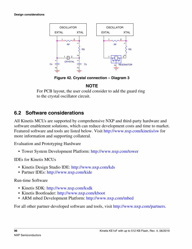
5
5
4
4
3
3
2
2
1
1
D D
C C
B B
A A
EXTAL XTAL OSCILLATOR
EXTAL XTAL OSCILLATOR
EXTAL XTAL OSCILLATOR EXTAL XTAL OSCILLATOR
EXTAL XTAL OSCILLATOR EXTAL XTAL OSCILLATOR
MCU
ADCx
MCU
ADCx
MCU
RESET_b
MCU
NMI_b
MCU
RESET_b
Supervisor Chip
OUT Active high, open drain
RESET_b
SWD_DIOSWD_CLK
Analog input
High voltage input
RESET_b
VDD
VDD
VDD
VDD
VDD
VDD
Drawing Title: Size Document Number Rev Date: Sheet of Page Title:
ICAP Classification: FCP: FIUO: PUBI:
SCH-XXXXX PDF: SPF-XXXXX X
<Title>
C Friday, February 06, 2015
<PageTitle>
1 1
___ ___ X Drawing Title: Size Document Number Rev Date: Sheet of Page Title:
ICAP Classification: FCP: FIUO: PUBI:
SCH-XXXXX PDF: SPF-XXXXX X
<Title>
C Friday, February 06, 2015
<PageTitle>
1 1
___ ___ X Drawing Title: Size Document Number Rev Date: Sheet of Page Title:
ICAP Classification: FCP: FIUO: PUBI:
SCH-XXXXX PDF: SPF-XXXXX X
<Title>
C Friday, February 06, 2015
<PageTitle>
1 1
___ ___ X
R
1 2
0.1uF
12
R51 2
Cx
12
0.1uF
12
RESONATOR
1 3
2Cy
12
Cx
12
CRYSTAL
21
J1
HDR_5X2
1 23 4
657 89 10
Cy
12
10k
12
10k
12
R412
CRYSTAL
21
0.1uF
12
10k
12
CRYSTAL
21
R11 2
R31 2
C
12
RESONATOR
1 3
2
R21 2
10k
12
10k
12
RF
1 2
RS
12
BAT54SW
1 2
3
RS
12
RS
12
C
12
RF
1 2
RS
1 2
RF
1 2
CRYSTAL
21
Figure 42. Crystal connection – Diagram 3
NOTEFor PCB layout, the user could consider to add the guard ringto the crystal oscillator circuit.
6.2 Software considerations
All Kinetis MCUs are supported by comprehensive NXP and third-party hardware andsoftware enablement solutions, which can reduce development costs and time to market.Featured software and tools are listed below. Visit http://www.nxp.com/kinetis/sw formore information and supporting collateral.
Evaluation and Prototyping Hardware
• Tower System Development Platform: http://www.nxp.com/tower
IDEs for Kinetis MCUs
• Kinetis Design Studio IDE: http://www.nxp.com/kds• Partner IDEs: http://www.nxp.com/kide
Run-time Software
• Kinetis SDK: http://www.nxp.com/ksdk• Kinetis Bootloader: http://www.nxp.com/kboot• ARM mbed Development Platform: http://www.nxp.com/mbed
For all other partner-developed software and tools, visit http://www.nxp.com/partners.
Design considerations
96 Kinetis KE1xF with up to 512 KB Flash, Rev. 4, 06/2019
NXP Semiconductors
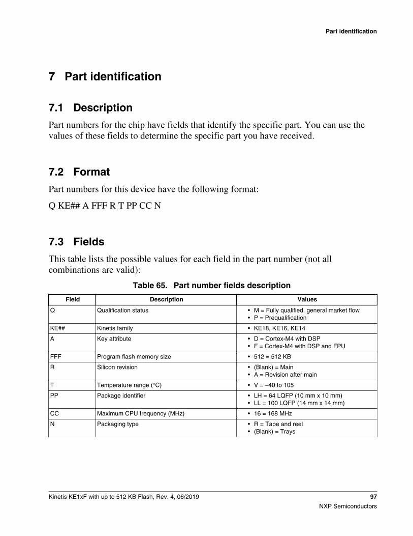
7 Part identification
7.1 Description
Part numbers for the chip have fields that identify the specific part. You can use thevalues of these fields to determine the specific part you have received.
7.2 Format
Part numbers for this device have the following format:
Q KE## A FFF R T PP CC N
7.3 Fields
This table lists the possible values for each field in the part number (not allcombinations are valid):
Table 65. Part number fields description
Field Description Values
Q Qualification status • M = Fully qualified, general market flow• P = Prequalification
KE## Kinetis family • KE18, KE16, KE14
A Key attribute • D = Cortex-M4 with DSP• F = Cortex-M4 with DSP and FPU
FFF Program flash memory size • 512 = 512 KB
R Silicon revision • (Blank) = Main• A = Revision after main
T Temperature range (°C) • V = –40 to 105
PP Package identifier • LH = 64 LQFP (10 mm x 10 mm)• LL = 100 LQFP (14 mm x 14 mm)
CC Maximum CPU frequency (MHz) • 16 = 168 MHz
N Packaging type • R = Tape and reel• (Blank) = Trays
Part identification
Kinetis KE1xF with up to 512 KB Flash, Rev. 4, 06/2019 97
NXP Semiconductors
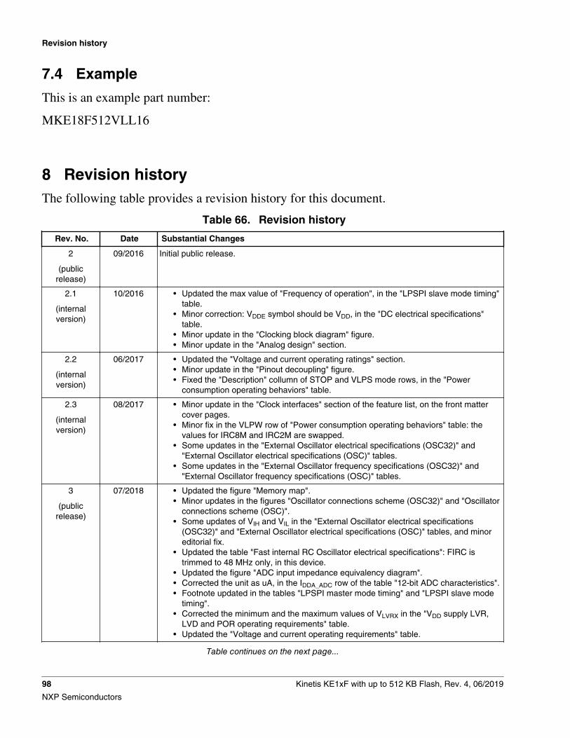
7.4 Example
This is an example part number:
MKE18F512VLL16
8 Revision historyThe following table provides a revision history for this document.
Table 66. Revision history
Rev. No. Date Substantial Changes
2
(publicrelease)
09/2016 Initial public release.
2.1
(internalversion)
10/2016 • Updated the max value of "Frequency of operation", in the "LPSPI slave mode timing"table.
• Minor correction: VDDE symbol should be VDD, in the "DC electrical specifications"table.
• Minor update in the "Clocking block diagram" figure.• Minor update in the "Analog design" section.
2.2
(internalversion)
06/2017 • Updated the "Voltage and current operating ratings" section.• Minor update in the "Pinout decoupling" figure.• Fixed the "Description" collumn of STOP and VLPS mode rows, in the "Power
consumption operating behaviors" table.
2.3
(internalversion)
08/2017 • Minor update in the "Clock interfaces" section of the feature list, on the front mattercover pages.
• Minor fix in the VLPW row of "Power consumption operating behaviors" table: thevalues for IRC8M and IRC2M are swapped.
• Some updates in the "External Oscillator electrical specifications (OSC32)" and"External Oscillator electrical specifications (OSC)" tables.
• Some updates in the "External Oscillator frequency specifications (OSC32)" and"External Oscillator frequency specifications (OSC)" tables.
3
(publicrelease)
07/2018 • Updated the figure "Memory map".• Minor updates in the figures "Oscillator connections scheme (OSC32)" and "Oscillator
connections scheme (OSC)".• Some updates of VIH and VIL in the "External Oscillator electrical specifications
(OSC32)" and "External Oscillator electrical specifications (OSC)" tables, and minoreditorial fix.
• Updated the table "Fast internal RC Oscillator electrical specifications": FIRC istrimmed to 48 MHz only, in this device.
• Updated the figure "ADC input impedance equivalency diagram".• Corrected the unit as uA, in the IDDA_ADC row of the table "12-bit ADC characteristics".• Footnote updated in the tables "LPSPI master mode timing" and "LPSPI slave mode
timing".• Corrected the minimum and the maximum values of VLVRX in the "VDD supply LVR,
LVD and POR operating requirements" table.• Updated the "Voltage and current operating requirements" table.
Table continues on the next page...
Revision history
98 Kinetis KE1xF with up to 512 KB Flash, Rev. 4, 06/2019
NXP Semiconductors
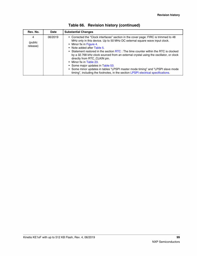
Table 66. Revision history (continued)
Rev. No. Date Substantial Changes
4
(publicrelease)
06/2019 • Corrected the "Clock interfaces" section in the cover page: FIRC is trimmed to 48MHz only in this device. Up to 50 MHz DC external square wave input clock.
• Minor fix in Figure 4.• Note added after Table 5.• Statement restored in the section RTC : The time counter within the RTC is clocked
by a 32.768 kHz clock sourced from an external crystal using the oscillator, or clockdirectly from RTC_CLKIN pin.
• Minor fix in Table 23.• Some major updates in Table 53.• Some minor updates in tables "LPSPI master mode timing" and "LPSPI slave mode
timing", including the footnotes, in the section LPSPI electrical specifications.
Revision history
Kinetis KE1xF with up to 512 KB Flash, Rev. 4, 06/2019 99
NXP Semiconductors

How to Reach Us:
Home Page:nxp.com
Web Support:nxp.com/support
Information in this document is provided solely to enable system and software implementers to useNXP products. There are no express or implied copyright licenses granted hereunder to design orfabricate any integrated circuits based on the information in this document. NXP reserves the right tomake changes without further notice to any products herein.
NXP makes no warranty, representation, or guarantee regarding the suitability of its products for anyparticular purpose, nor does NXP assume any liability arising out of the application or use of anyproduct or circuit, and specifically disclaims any and all liability, including without limitationconsequential or incidental damages. "Typical" parameters that may be provided in NXP data sheetsand/or specifications can and do vary in different applications, and actual performance may vary overtime. All operating parameters, including "typicals," must be validated for each customer applicationby customer's technical experts. NXP does not convey any license under its patent rights nor therights of others. NXP sells products pursuant to standard terms and conditions of sale, which can befound at the following address: nxp.com/SalesTermsandConditions.
While NXP has implemented advanced security features, all products may be subject to unidentifiedvulnerabilities. Customers are responsible for the design and operation of their applications andproducts to reduce the effect of these vulnerabilities on customer's applications and products, andNXP accepts no liability for any vulnerability that is discovered. Customers should implementappropriate design and operating safeguards to minimize the risks associated with their applicationsand products.
NXP, the NXP logo, NXP SECURE CONNECTIONS FOR A SMARTER WORLD, COOLFLUX,EMBRACE, GREENCHIP, HITAG, I2C BUS, ICODE, JCOP, LIFE VIBES, MIFARE, MIFARECLASSIC, MIFARE DESFire, MIFARE PLUS, MIFARE FLEX, MANTIS, MIFARE ULTRALIGHT,MIFARE4MOBILE, MIGLO, NTAG, ROADLINK, SMARTLX, SMARTMX, STARPLUG, TOPFET,TRENCHMOS, UCODE, Freescale, the Freescale logo, AltiVec, C‑5, CodeTEST, CodeWarrior,ColdFire, ColdFire+, C‑Ware, the Energy Efficient Solutions logo, Kinetis, Layerscape, MagniV,mobileGT, PEG, PowerQUICC, Processor Expert, QorIQ, QorIQ Qonverge, Ready Play, SafeAssure,the SafeAssure logo, StarCore, Symphony, VortiQa, Vybrid, Airfast, BeeKit, BeeStack, CoreNet,Flexis, MXC, Platform in a Package, QUICC Engine, SMARTMOS, Tower, TurboLink, UMEMS, eIQ,Immersiv3D, EdgeLock, and EdgeScale are trademarks of NXP B.V. All other product or servicenames are the property of their respective owners. AMBA, Arm, Arm7, Arm7TDMI, Arm9, Arm11,Artisan, big.LITTLE, Cordio, CoreLink, CoreSight, Cortex, DesignStart, DynamIQ, Jazelle, Keil, Mali,Mbed, Mbed Enabled, NEON, POP, RealView, SecurCore, Socrates, Thumb, TrustZone, ULINK,ULINK2, ULINK-ME, ULINK-PLUS, ULINKpro, µVision, Versatile are trademarks or registeredtrademarks of Arm Limited (or its subsidiaries) in the US and/or elsewhere. The related technologymay be protected by any or all of patents, copyrights, designs and trade secrets. All rights reserved.Oracle and Java are registered trademarks of Oracle and/or its affiliates. The Power Architecture andPower.org word marks and the Power and Power.org logos and related marks are trademarks andservice marks licensed by Power.org.
©2015–2019 NXP B.V.
Document Number KE1xFP100M168SF0Revision 4, 06/2019