Embed Size (px)
Citation preview
i
Klystron Switching Power Supplies
for the International Linear Collider
Andrea Fraioli
Masterrsquos Degree Dissertation
December 2009
ii
DISSERTATION ABSTRACT
Klystron Switching Power Supplies
For the International Linear Collider
dott Andrea Fraioli
Supervisor Supervisor Prof Giovanni Busatto Prof Carmine E Pagliarone
Electrical Engineering Masterrsquos Degree
At the
UNIVERSITY OF CASSINO FACULTY OF ENGINEERING
December 2009
The International Linear Collider is a majestic High Energy Physics particle accelerator that will give physicists a new cosmic doorway to explore energy regimes beyond the reach of todayrsquos accelerators ILC will complement the Large Hadron Collider (LHC) a proton-proton collider at the European Center for Nuclear Research (CERN) in Geneva Switzerland by producing electron-positron collisions at center of mass energy of about 500 GeV In particular the subject of this dissertation is the RampD for a solid state Marx Modulator and relative switching power supply for the International Linear Collider Main LINAC Radio Frequency stations
iii
Acknowledgements
I would like to express my gratitude to Prof Carmine Elvezio Pagliarone His continuous supervision during my work at Fermi National Accelerator Laboratory (Fermilab) and before has been for me very important and intellectually a pleasure He guided me through all different aspects of Particle Accelerator Collider Physics and in particular on our intense RampD on a Solid State Marx Modulator for the ILC Klystron Modulators I would like to extend my gratitude to Prof Giovanni Busatto for his supervision during my work at University of Cassino His knowledge of power electronics devices has guided me during the Switch in Line Converter project Besides I want express my gratitude to the NTA-ILC Pisa Group Leader Dott Franco Bedeschi for supporting us in this RampD activity and then to Prof Giovanni Maria Piacentino the senior Cassino University physicist for the support and collaboration in the Cassino Group At the end a special thanks goes to Fermi National Accelerator Laboratory for technical support during this research activity
iv
Dedication
A mia Madre ed a mio Padre per aver dedicato tutto il loro amore e tutti i loro sacrific quotidiani a me e a mio Fratello dedico questa tesi quale frutto di un intenso lavoro intellettuale prolifico di soddisfazioni
v
Table of Contents Abstract ii Acknowledgements iii Dedication iv Index v List of Tables viii List of Figures ix
vi
INDEX
1 Physics motivations for the International Linear Collider 11 Introduction ` 1 12 Higgs Boson Physics 2 13 Dark Matter amp Extra Dimension 5
2 The ILC accelerator Design 21 Electron and positron sources 8 22 Service Rings 10
221 Damping Rings 12 222 Ring to Main Linac 12
23 Main Linac 15 24 The ILC Accelerating system 16
241 Superconducting cavities 17 242 RF distribution system 17 243 Klystron 19 244 Klystron Modulator 21 245 The cryogenic systems 24
25 Estimate for construction of ILC 26
3 Klystron Modulator Power Supplies 31 Modulator charging power supply design requirements 35 32 Modulator power supply design analysis 37
321 TESLA design 37 322 A Russian design for TESLA 39 323 Fermilab Power Supply 42 324 SCR bridge in series with a diode rectifier 43
3241 SCR bridge with single phase control 44 3242 Digital regulation 46
325 Series connection of buck converters 50 33 The Buck converter solution 51
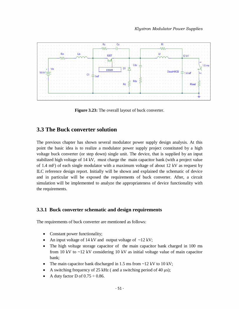
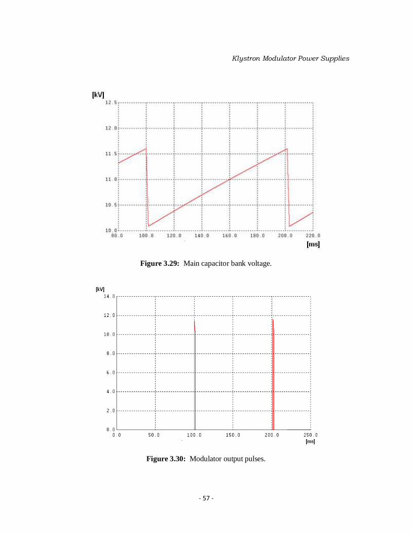
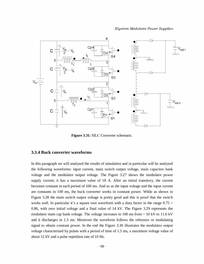
331 Buck converter schematic and design requirements 51 332 Circuit simulation and analysis 52 333 Main switch control for constant power 53 334 Buck converter waveforms 58
34 The Switch In Line Converter 59 341 Operation Principle 59 342 30 kW SILC Project 61
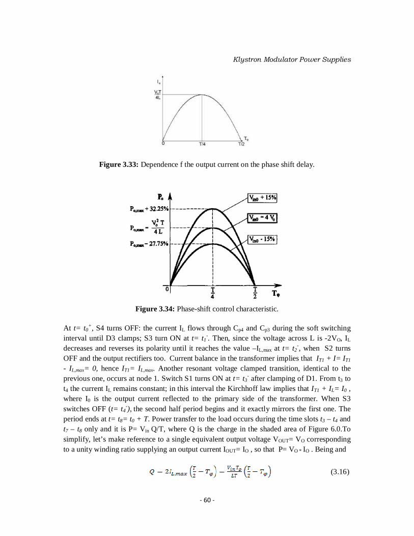
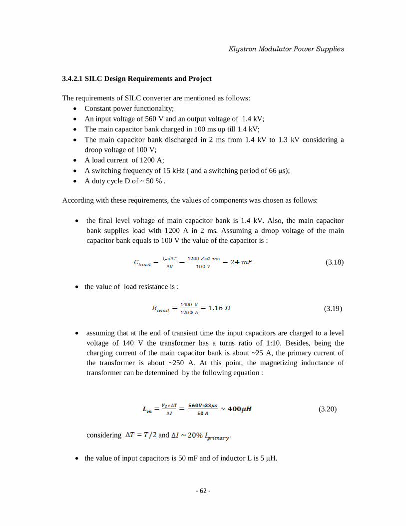
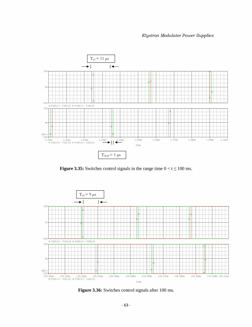
3421 SILC design requirements and Project 62 3422 Circuit simulation and analysis 64 3423 Control signals of switches 64
vii
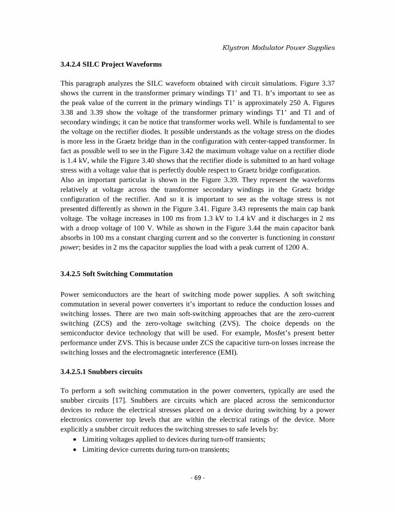
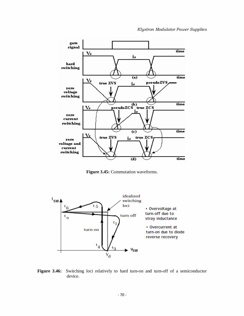
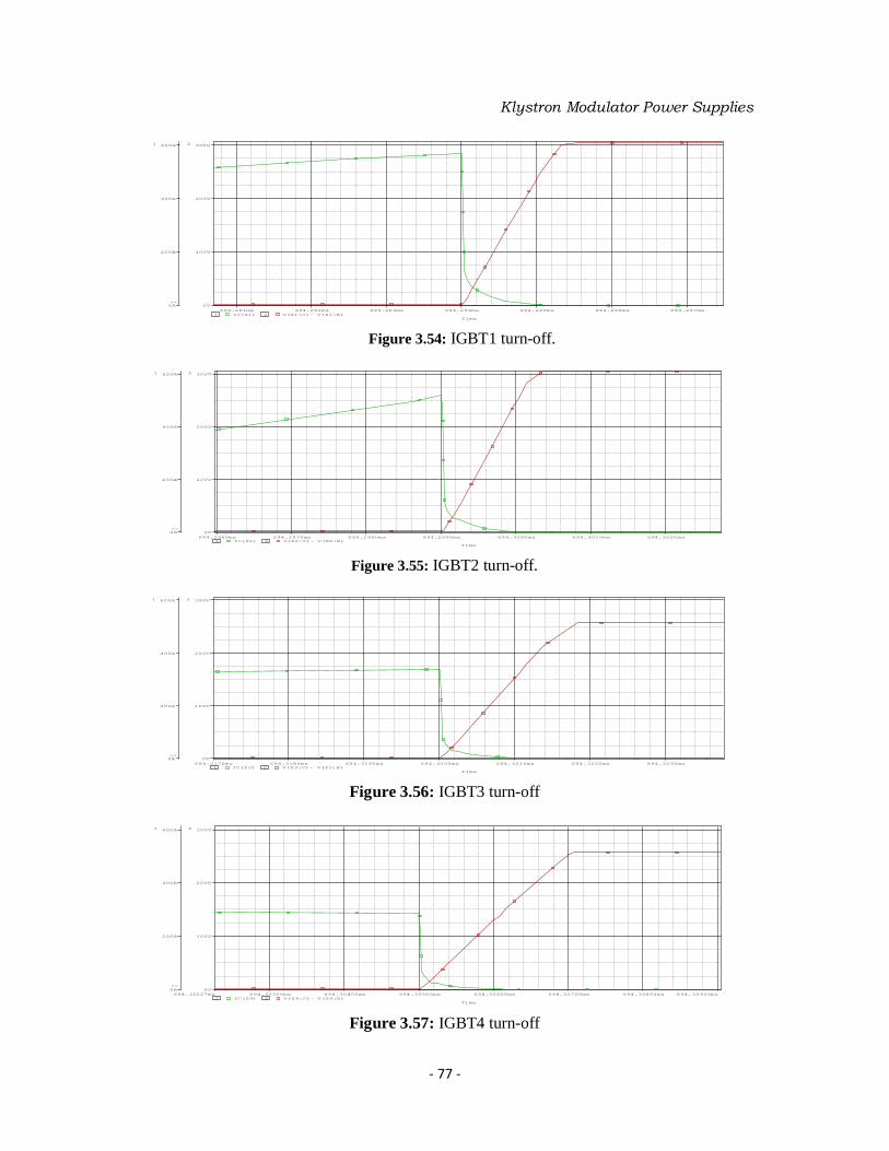
3424 SILC waveforms 69 3425 Soft switching commutation 69
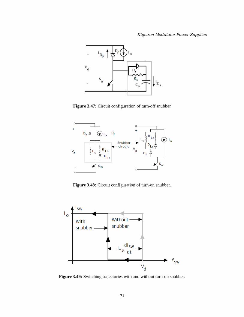
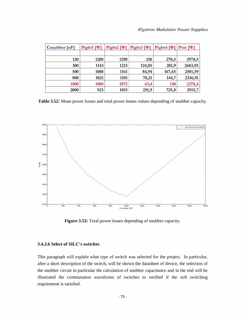
34251 Snubbers circuits 69 3426 Select of SILCrsquos switches 75
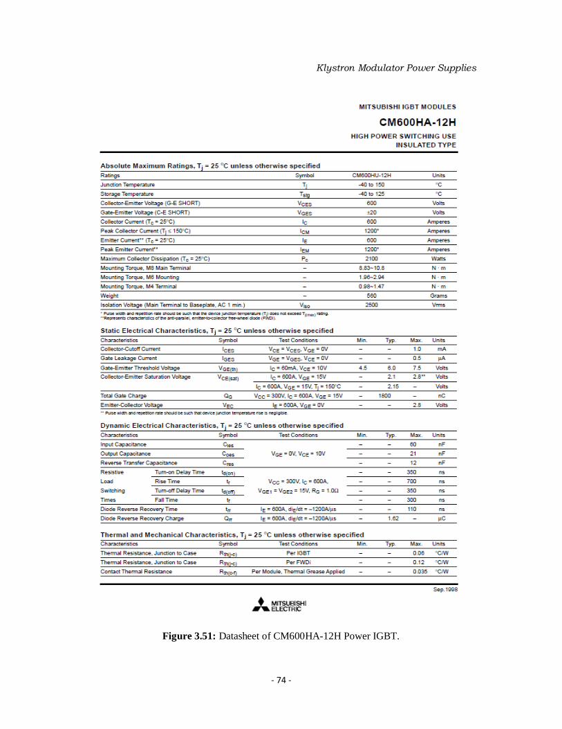
34261 Insulated Gate Bipolar Transistors (IGBTs) 76 34262 Choose of snubber capacity and switching commutations 76
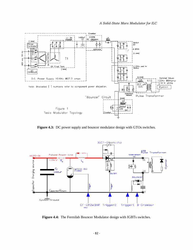
4 A Solid State Marx Modulator for ILC 41 Introduction 79 42 The Fermilab Bouncer Modulator 79
421 Operation principle 81 422 The Bouncer Modulator key components and costs 81
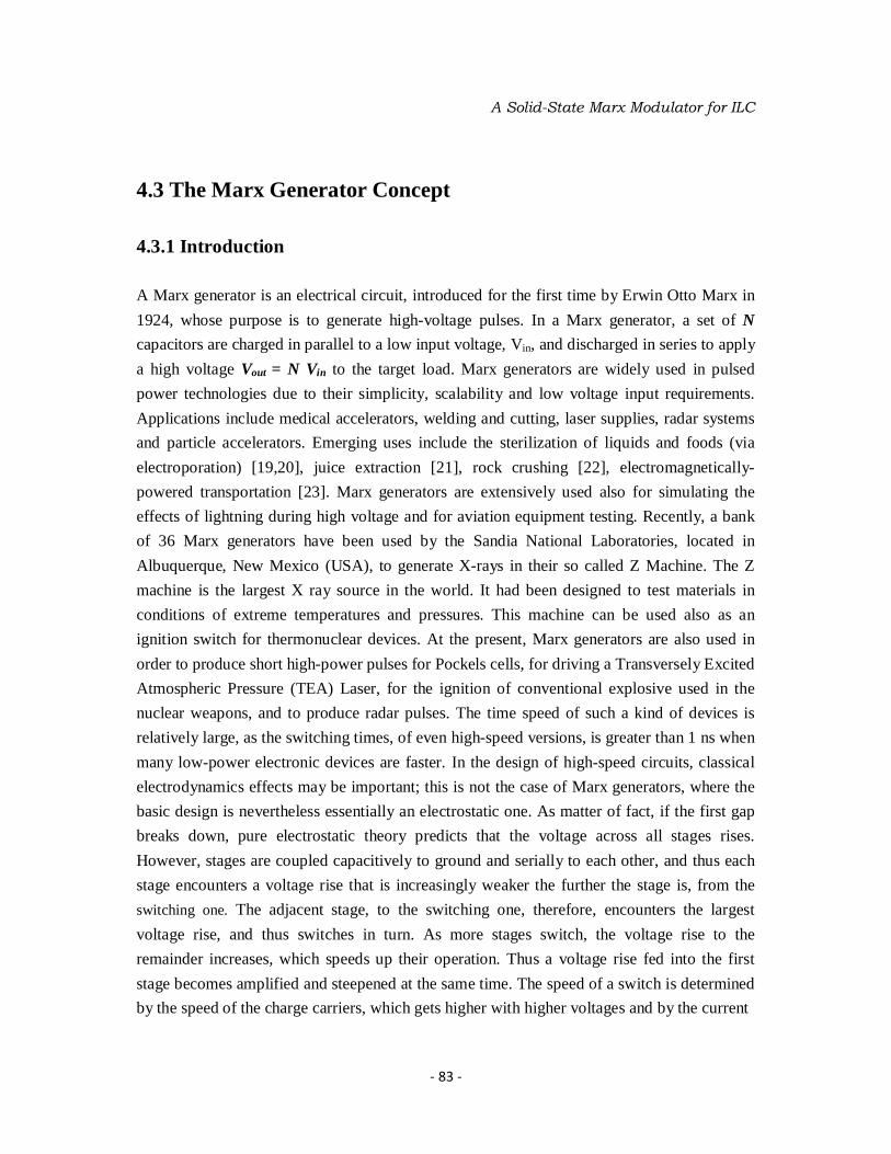
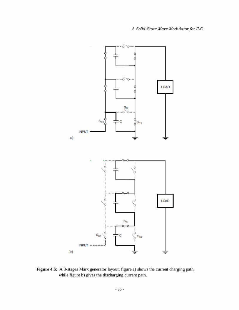
43 The Marx Generator Concept 83 431 Introduction 83 432 The classical layout 84 433 Solid State Marx Generator 86
44 A SM2 Solid State Marx Modulator for ILC 87 441 The SM2 fundamental cell design 89 442 The SM2 Main Marx generator 90
4421 The Main Marx Layout and Design Requirements 90 4422 Stray Capacitance Charging Losses 92 4423 Main Marx output response 92
443 The Flattener circuit 94 444 The SM2 Switching Trigger System 96
45 Solid State Marx Modulator Single Failure Risks 98 46 SM2 Modulator circuit simulations and analysis 99 47 Conclusions 100
Appendix A The synchrotron radiation energy loss 104 B The concept of luminosity 109
Bibliography
viii
LIST OF TABLES 201 Electrons Source System parameters 11
202 Nominal Positron Source parameters 11
203 Positron Damping Ring parameters the Electron Damping Ring is identical except for a smaller injected emittance
13
204 Basic beam parameters of the RTML 15
205 Nominal beam parameters in the ILC Main Linac 16
206 ILC 9-cell Superconducting Cavity layout parameters 18
207 Properties of high-RRR (residual resistivity ratio) Niobium suitable for use in ILC Cavities
18
208 RF Unit parameters 20
209 10MW MBK parameters 22
210 Modulator Specifications amp Requirements Assuming Klystron microP=338 Effy= 65
25
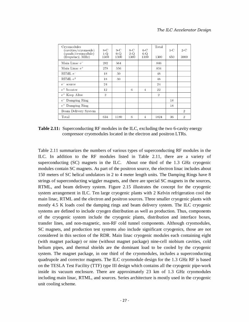
211 Superconducting RF modules in the ILC excluding the two 6-cavity energy compressor cryomodules located in the electron and positron LTRs
27
212 Possible division of responsibilities for the 3 sample sites (ILC Units) 31
213 Distribution of the ILC Value Estimate by area system and common infrastructure in ILC Units The estimate for the experimental detectors for particle physics is not included
32
214 Explicit labor which may be supplied by collaborating laboratories or institutions listed by Global Technical and some Area-specific Systems
33
215 Composition of the management structure at ILC 34
ix
LIST OF FIGURES 101 Feynman diagrams for Higgsstrahlung (top) and WW fusion (bottom) Right cross
sections of the two processes as function of the center of mass energy for Higgs masses of 200 and 320 GeVc2
2
102 SM and MSSM predictions for gttH versus gWWH and expected precision of the corresponding LHC and ILC measurements
4
103 Reconstructed mass sum and difference for HArarr 4b for masses of mH = 250 GeVc2 and mA = 300 GeVc2 at a center of mass energy of 800 GeVc2
4
104 Left Production mechanism for e+e-rarr γG the graviton escapes into extra dimensions Right The cross section of this process as a function of the center of mass energy for different numbers of extra dimensions The points with error bars indicate the precision of the ILC measurements
6
105 Dark matter relic density versus WIMP mass in the LCC1 SUSY scenario Possible parameter choices are indicated as black dots which are compared to the sensitivity of present and future measurements from satellite and accelerator based experiments
6
201 A schematic layout of the International Linear Collider 9
202 Cutaway view of the linac dual-tunnel configuration On the left you can see the Main Linac tunnel on the right the service tunnel hosting the klystrons the klystron modulators and switching power supplies
9
203 Schematic view of the polarized Electron Source 10
204 Overall layout of the Positron Source 12
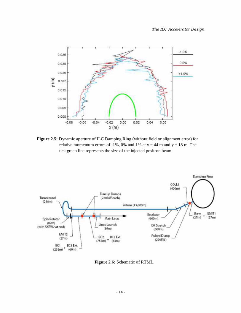
205 Dynamic aperture of ILC Damping Ring (without field or alignment error) for relative momentum errors of -1 0 and 1 at x = 44 m and y = 18 m The tick green line represents the size of the injected positron beam
14
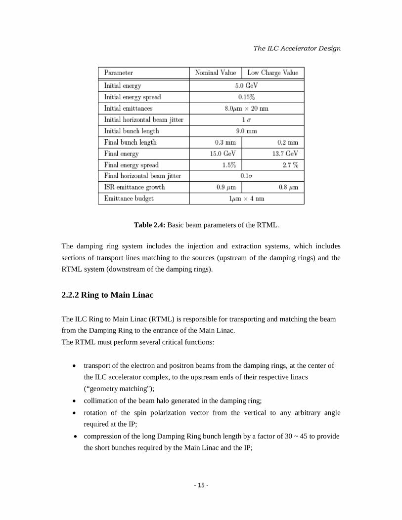
206 Schematic of RTML 14
207 9-cells Superconducting RF Cavity 17
208 RF unit diagram showing the basic waveguide distribution layout between the klystron and 26 cavities in three cryomodules
19
209 Waveguide circuit from tap-off hybrid to coupler input showing the various components (except for the directional coupler)
21
210 Toshiba 3736 Multi-Beam Klystron 21
211 a) CPI VKL-8301 b) Thales TH 1801 c) Toshiba MBK E3736 23
212 Test results for a) CPI VKL-8301 at reduced pulse width b) Toshiba MBK E3736 at full spec pulse width c) Thales TH1801 at reduced pulse width
24
x
213 a) Capacitor Stack b) Dual IGBT Switch c) Bouncer Choke d) Pulse transformer 24
214 Damping Ring 12 MW RF station (1 of 20) 25
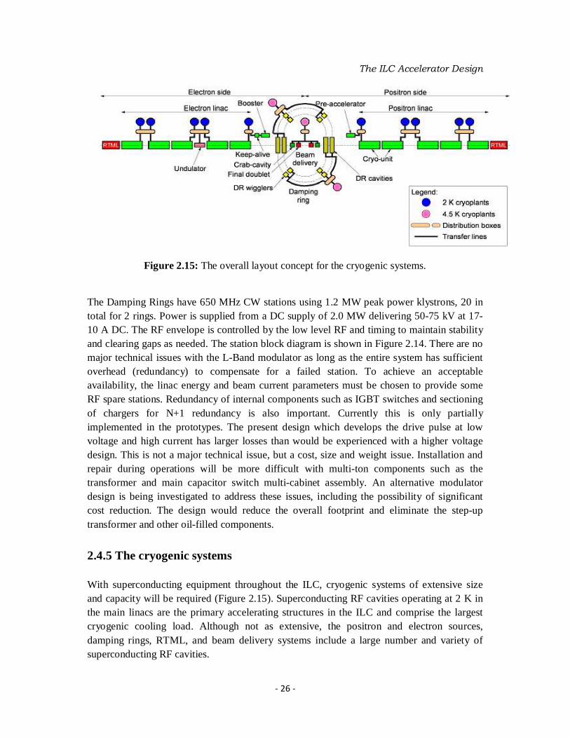
215 The overall layout concept for the cryogenic systems 26
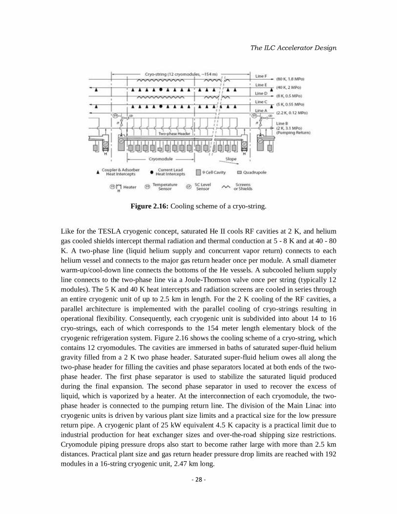
216 Cooling scheme of a cryo-string 28
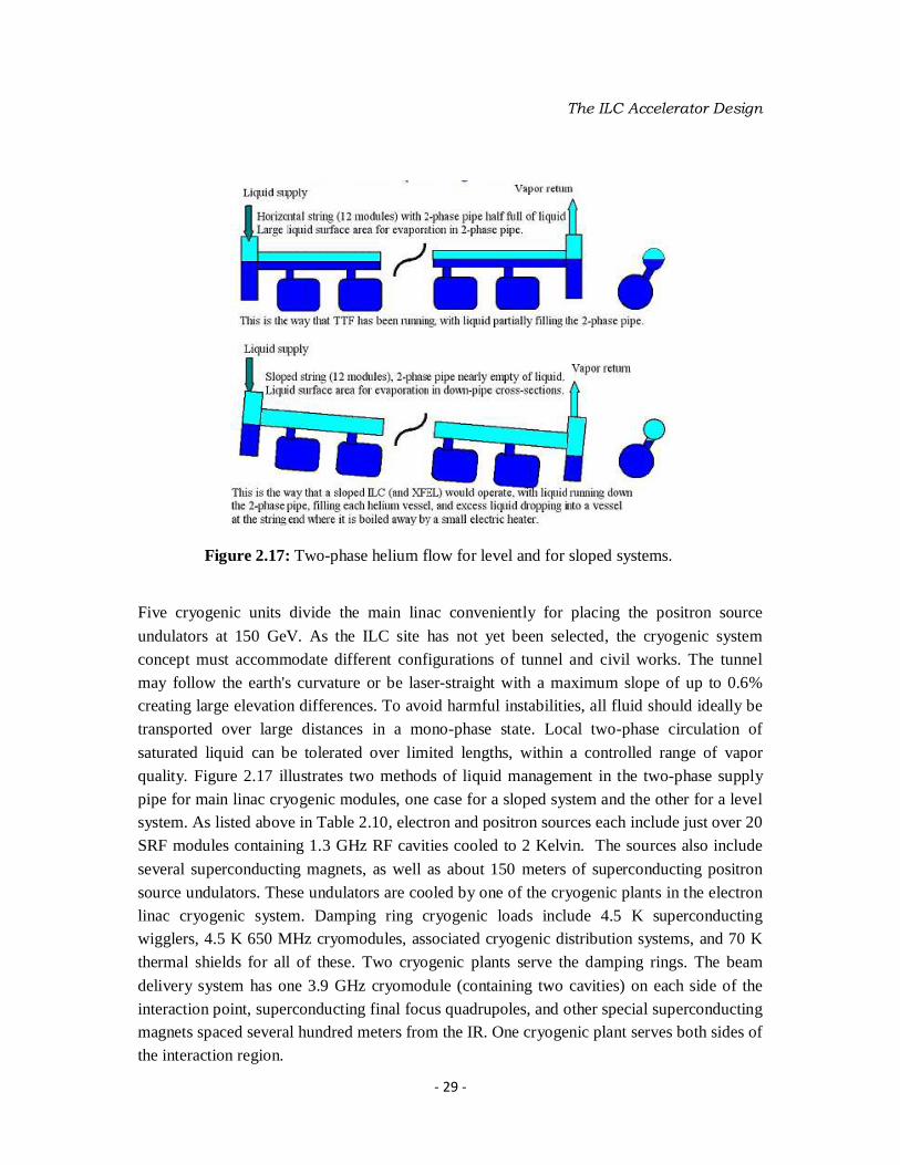
217 Two-phase helium flow for level and for sloped systems 29
218 Distribution of the ILC value estimate by area system and common infrastructure in ILC Units The estimate for the experimental detectors for particle physics is not included
30
219 Explicit labor which may be supplied by collaborating laboratories or institutions listed by Global Technical and some Area-specific Systems
32
301 Schematic of the series resonance sine converter 36
302 Equivalent circuit of the power supply 36
303 Series resonance sine converter with only one capacitor 36
304 Voltage and current function of the half bridge 37
305 Voltage and current waveform of power supply 38
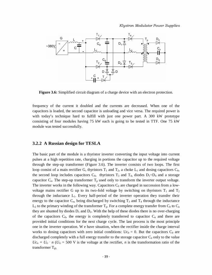
306 Simplified circuit diagram of a charge device with an electron protection 39
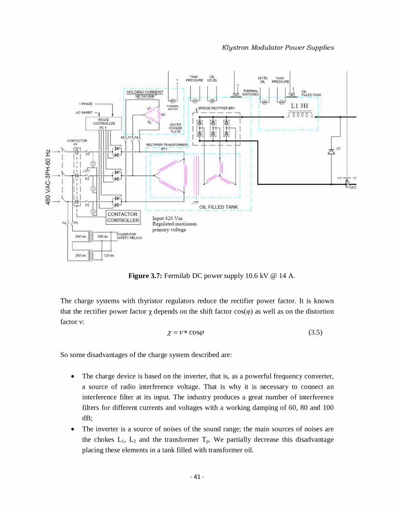
307 Fermilab DC power supply 106 kV 14 A 41
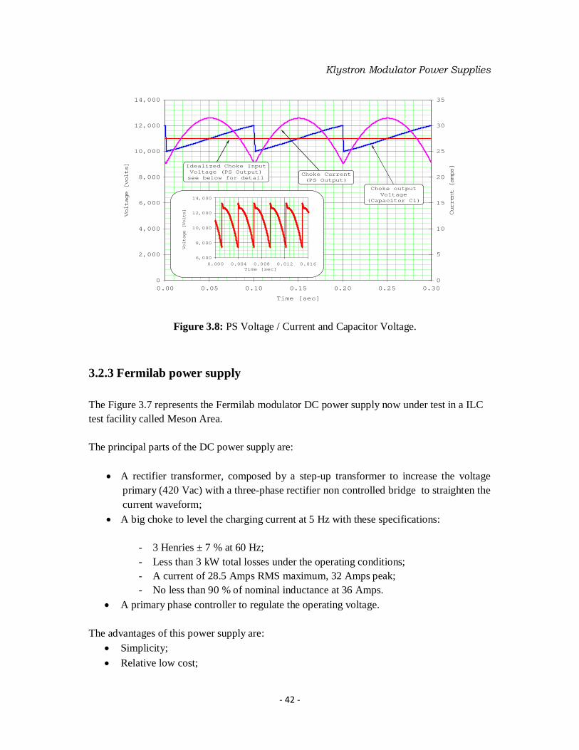
308 PS Voltage Current and Capacitor Voltage 42
309 Series connection of a diode and a SCR bridge 43
310 Voltage curve form of the main capacitor bank in the modulator 43
311 Voltage curve of series connection of diode and SCR bridge 44
312 Real and reactive power in dependence of the phase angle α 45
313 Power diagram of a series connection of a diode and SCR bride α(P) 46
314 Simplified modulator circuit 46
315 Voltage curve of the main capacitor 47
316 Stored reference charging curve of the capacitor 47
317 Input power of the modulator 47
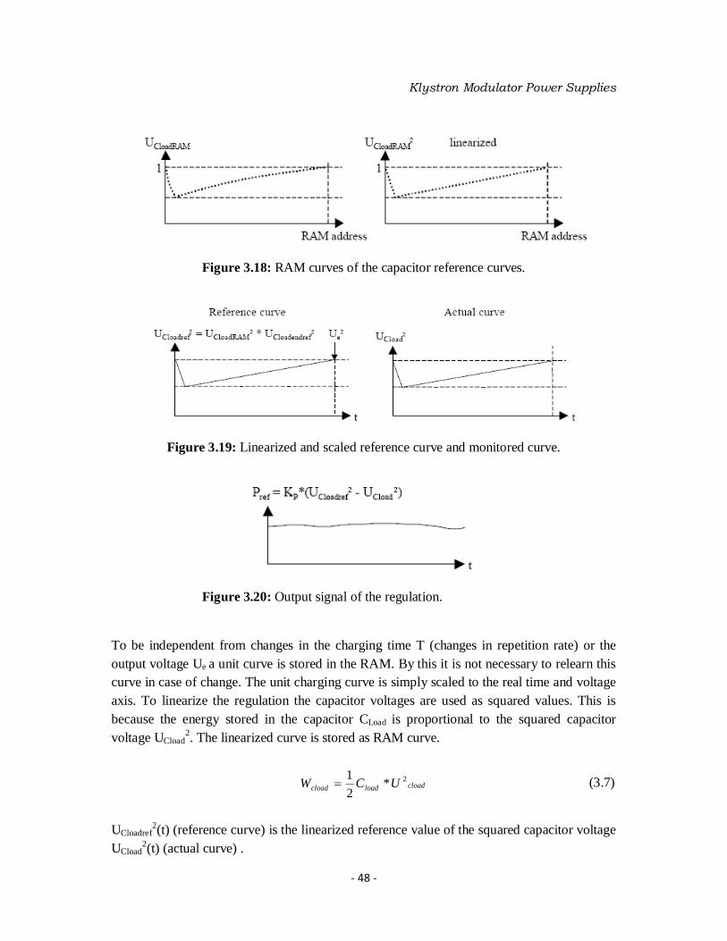
318 RAM curves of the capacitor reference curves 48
xi
319 Linearized and scaled reference curve and monitored curve 48
320 Output signal of the regulation 48
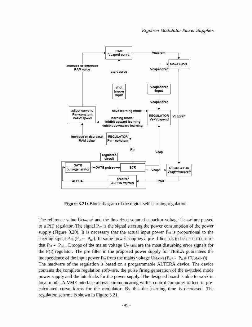
321 Block diagram of the digital self-learning regulation 49
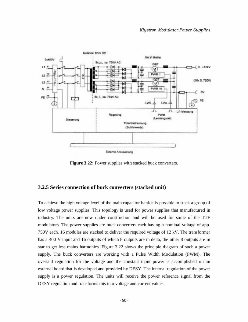
322 Power supplies with stacked buck converters 50
323 The overall layout of buck converter 51
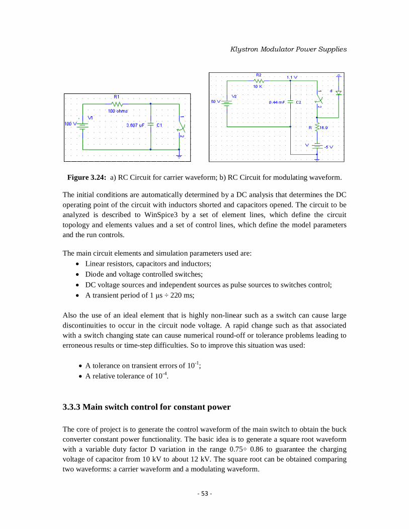
324 a) RC Circuit for carrier waveform b) RC Circuit for modulating waveform 53
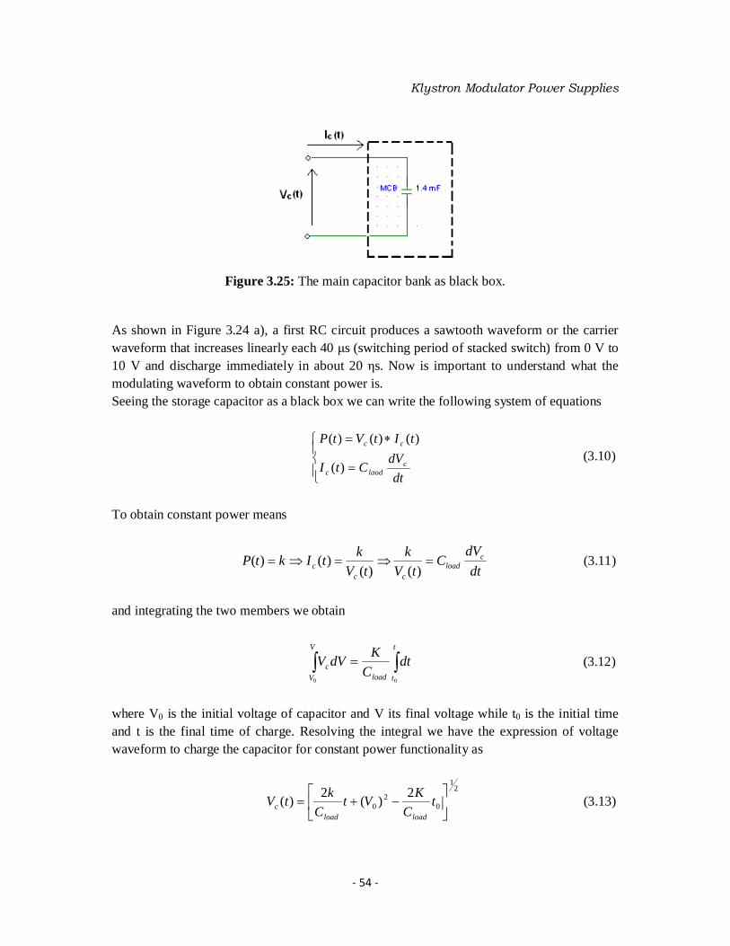
325 The main capacitor bank as black box 54
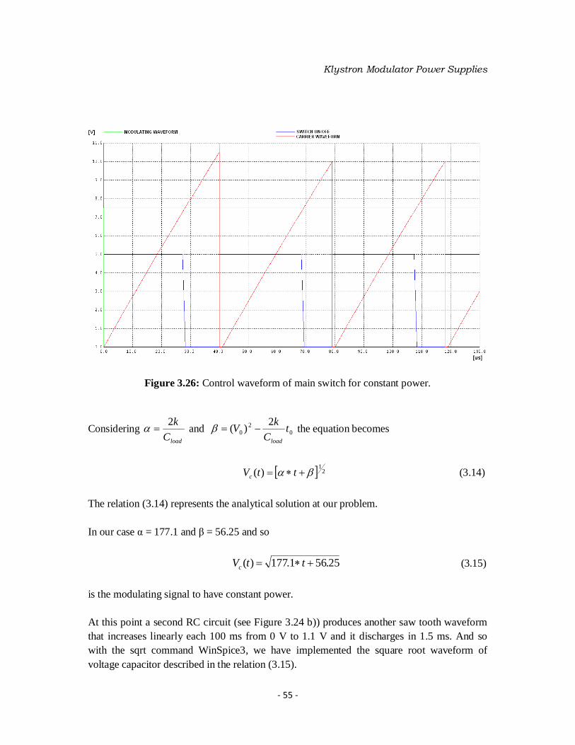
326 Control waveform of main switch for constant power 55
327 Buck converter input current 56
328 Main switch output voltage 56
329 Main capacitor bank voltage 57
330 Modulator output pulses 57
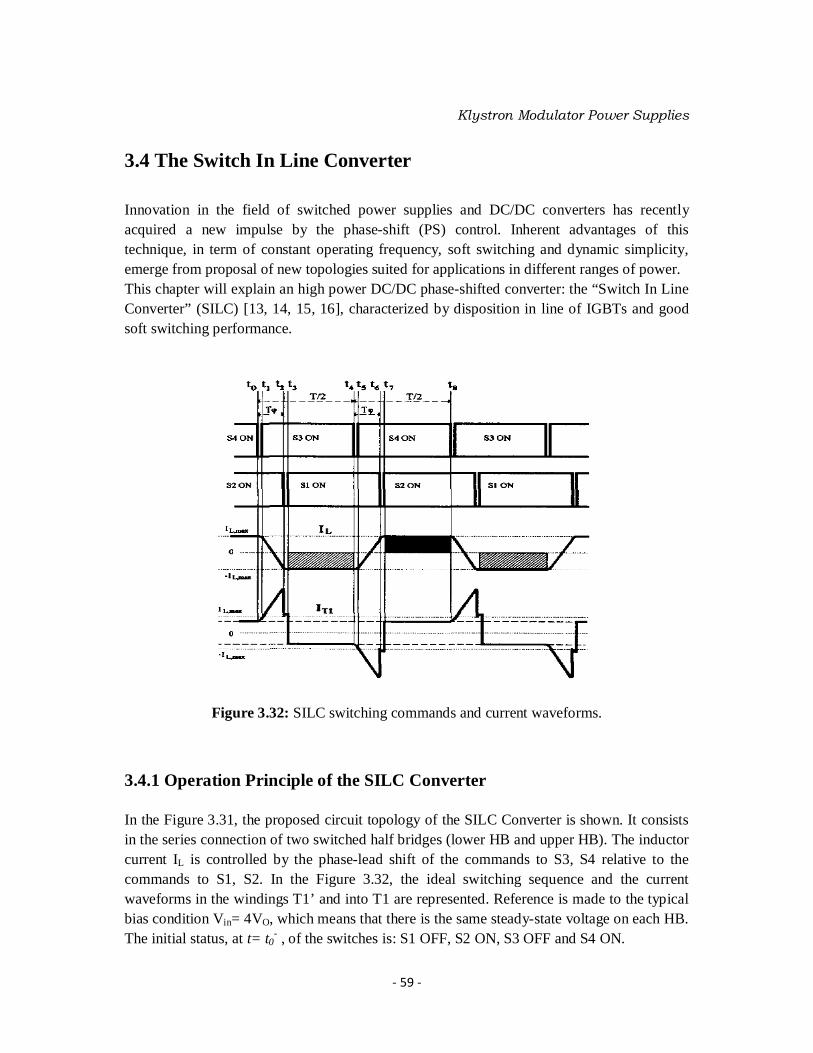
331 SILC Converter schematic 58
332 SILC switching commands and current waveforms 59
333 Dependence of the output current on the phase shift delay 60
334 Phase-shift control characteristic 60
335 Switches control signals in the range time 0 lt t le 100 ms 63
336 Switches control signals after 100 ms 63
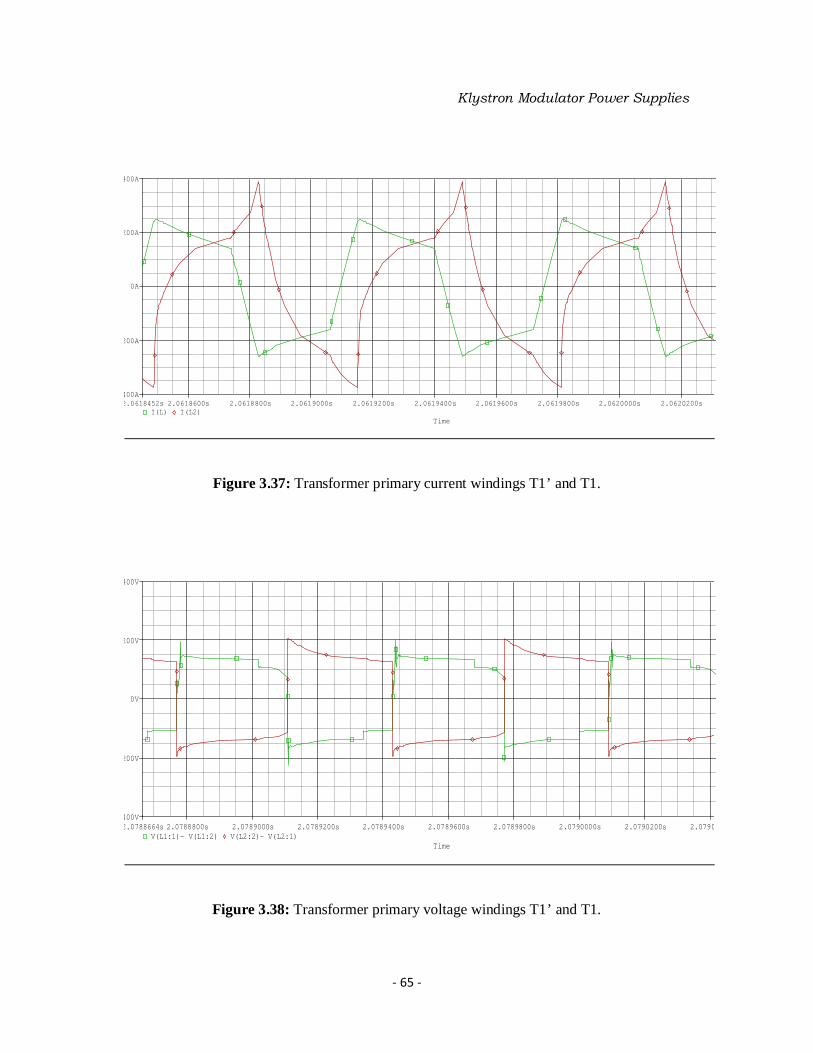
337 Transformer current primary windings T1rsquo and T1 65
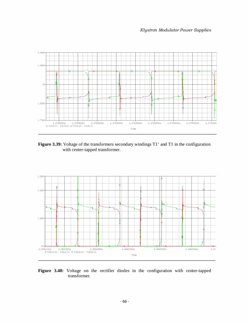
338 Transformers voltage primary windings T1rsquo and T1 65
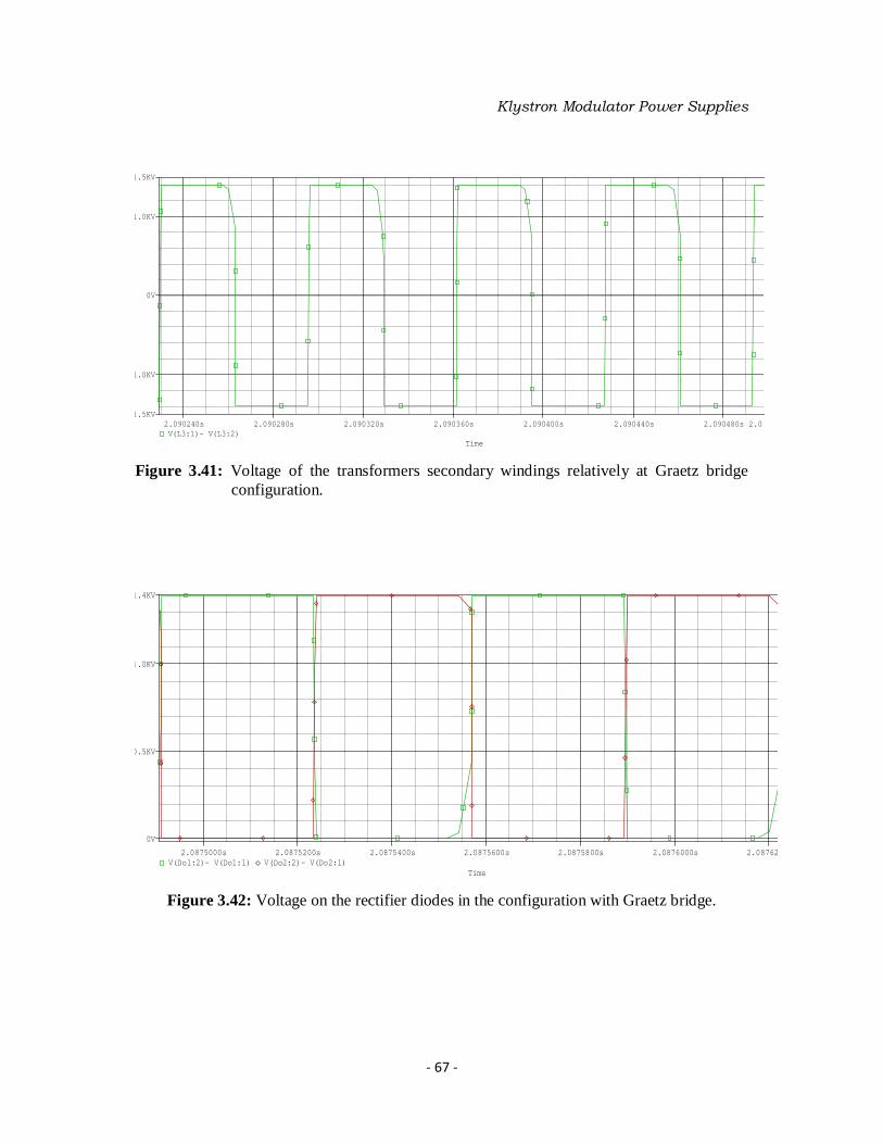
339 Voltage of the transformers secondary windings T1rsquo and T1 in the configuration with center-tapped transformer
66
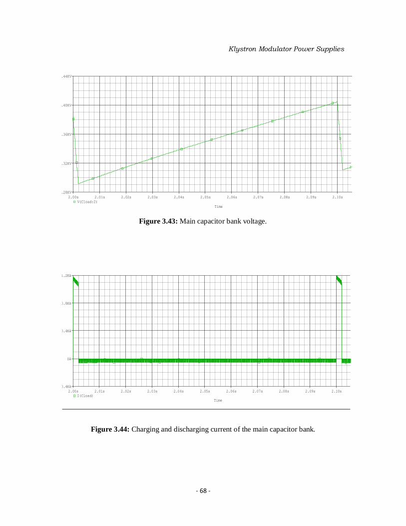
340 Voltage on the rectifier diodes in the configuration with center-tapped transformer 66
341 Voltage of the transformers secondary windings relatively at Graetz bridge configuration
67
342 Voltage on the rectifier diodes in the configuration with Graetz bridge 67
343 Main capacitor bank voltage 68
344 Charging and discharging current of the main capacitor bank 68
xii
345 Commutation waveforms 70
346 Switching loci relatively to hard turn-on and turn-off of a semiconductor device 70
347 Circuit configuration of turn-off snubber 71
348 Circuit configuration of turn-on snubber 71
349 Switching trajectories with and without turn-on snubber 71
350 IGBT circuit symbol and equivalent circuit 72
351 Datasheet of CM600HA-12H Power IGBT 74
353 Total power losses depending of snubber capacity 75
354 IGBT1 turn-off 77
355 IGBT2 turn-off 77
356 IGBT3 turn-off 77
357 IGBT4 turn-off 77
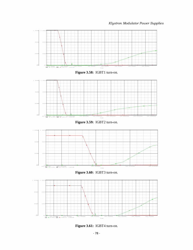
358 IGBT1 turn-on 78
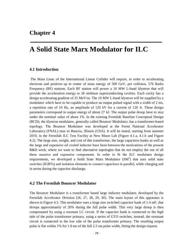
359 IGBT2 turn-on 78
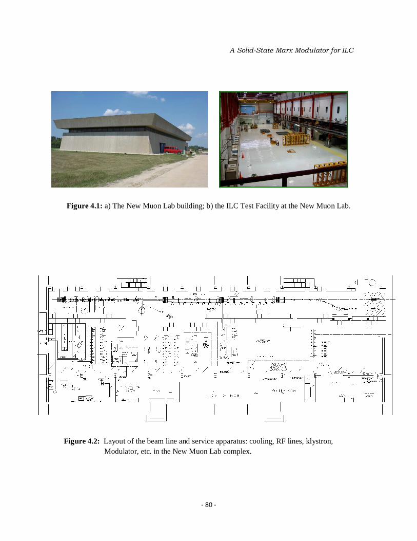
360 IGBT3 turn-on 78
361 IGBT4 turn-on 78
401 a) The New Muon Lab building b) the ILC Test Facility at the New Muon Lab 80
402 Layout of the beam line and service apparatus cooling RF lines klystron Modulator etc in the New Muon Lab complex
80
403 DC power supply and bouncer modulator design with GTOs switches 82
404 The Fermilab Bouncer Modulator design with IGBTs switches 82
405 A classical 4-stages Marx generator circuit 84
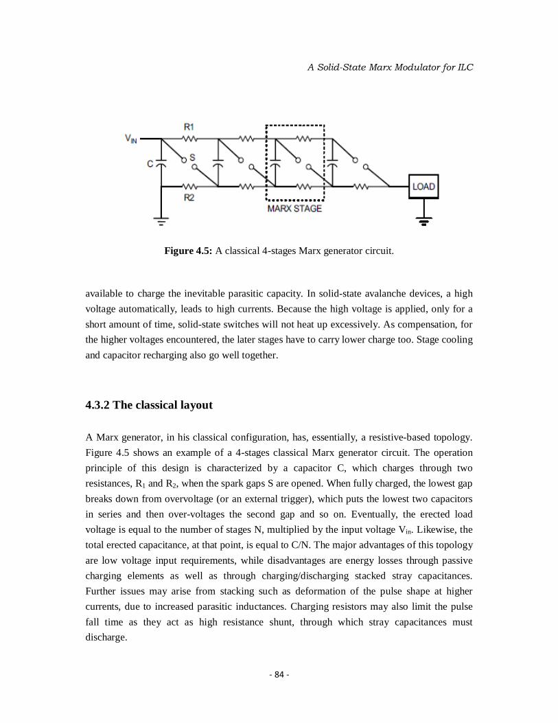
406 A 3-stages Marx generator layout figure a) shows the current charging path while figure b) gives the discharging current path
85
407 An example of 3-stages Solid State Marx Bank emp88loying ideal charge and discharge IGBTs (SC and SD)
86
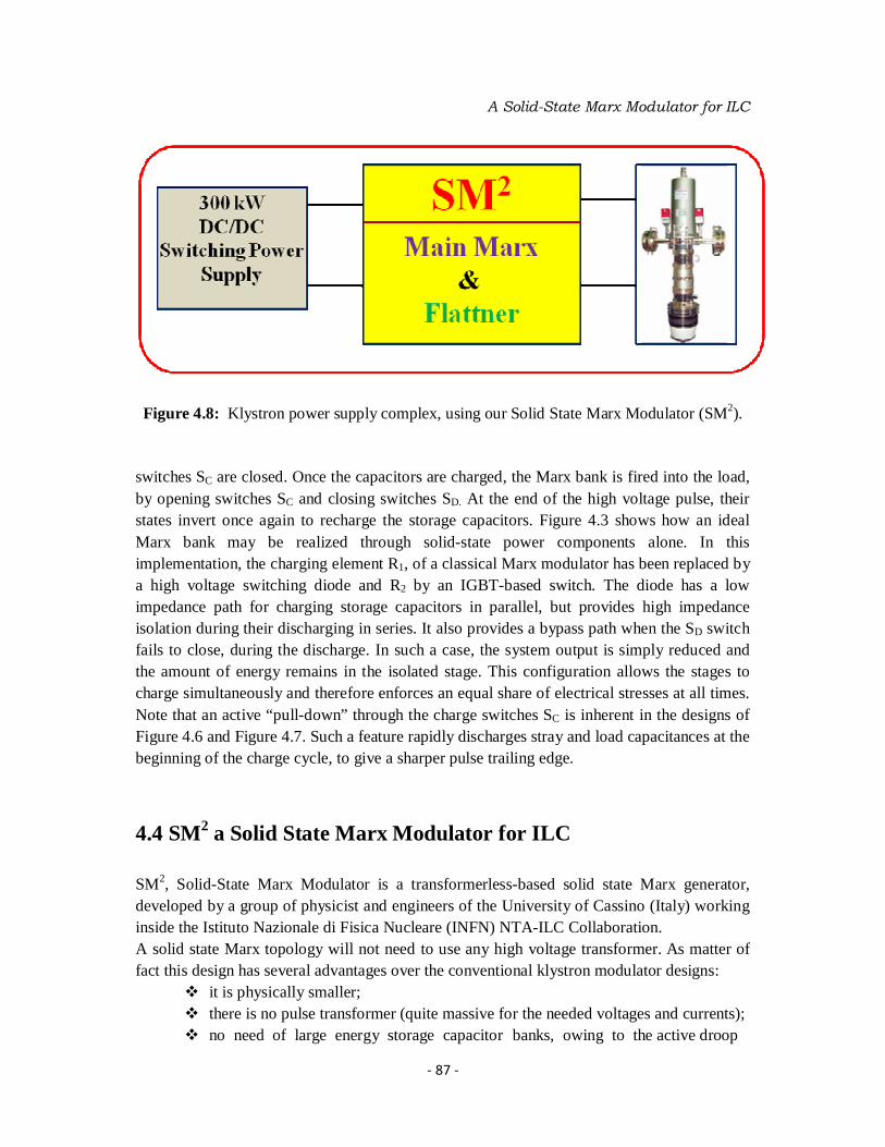
408 Klystron power supply complex using our Solid State Marx Modulator (SM2) 87
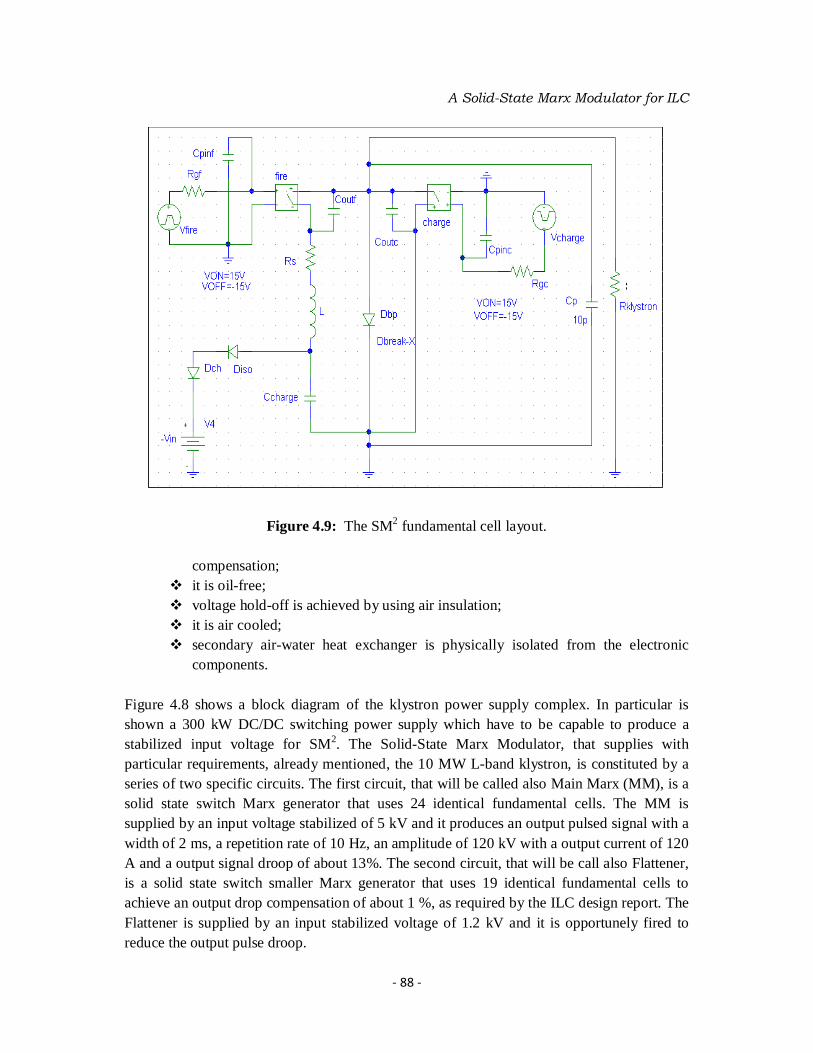
409 The SM2 fundamental cell layout 88
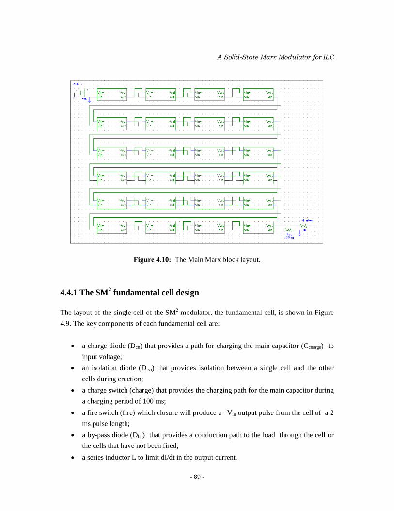
410 The Main Marx block layout 89
xiii
411 Marx bank efficiency versus the number of Marx stages for various stray stage capacitances The inset shows a close-up of 10-stages modulator efficiency
90
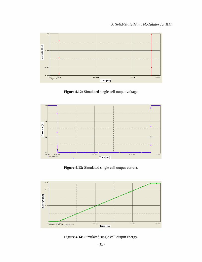
412 Simulated single cell output voltage 91
413 Simulated single cell output current 91
414 Simulated single cell output energy 91
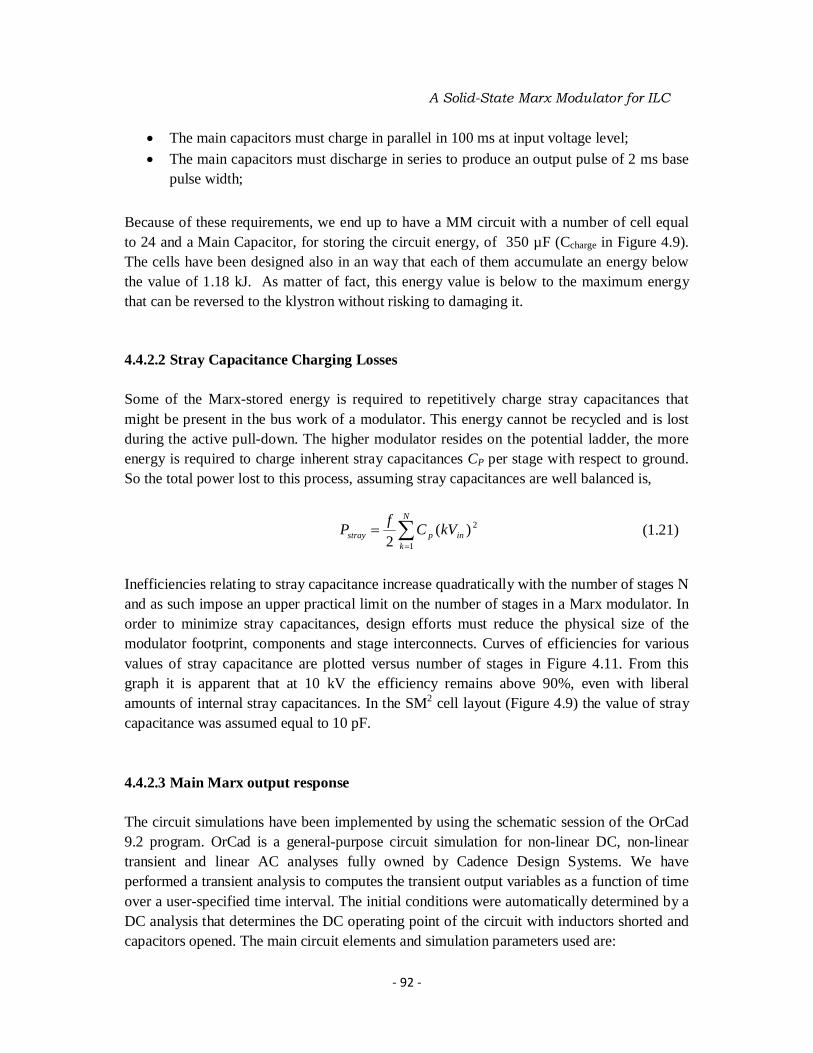
415 Simulated Main Marx output voltage the droop in the output voltage has a value of about 13
93
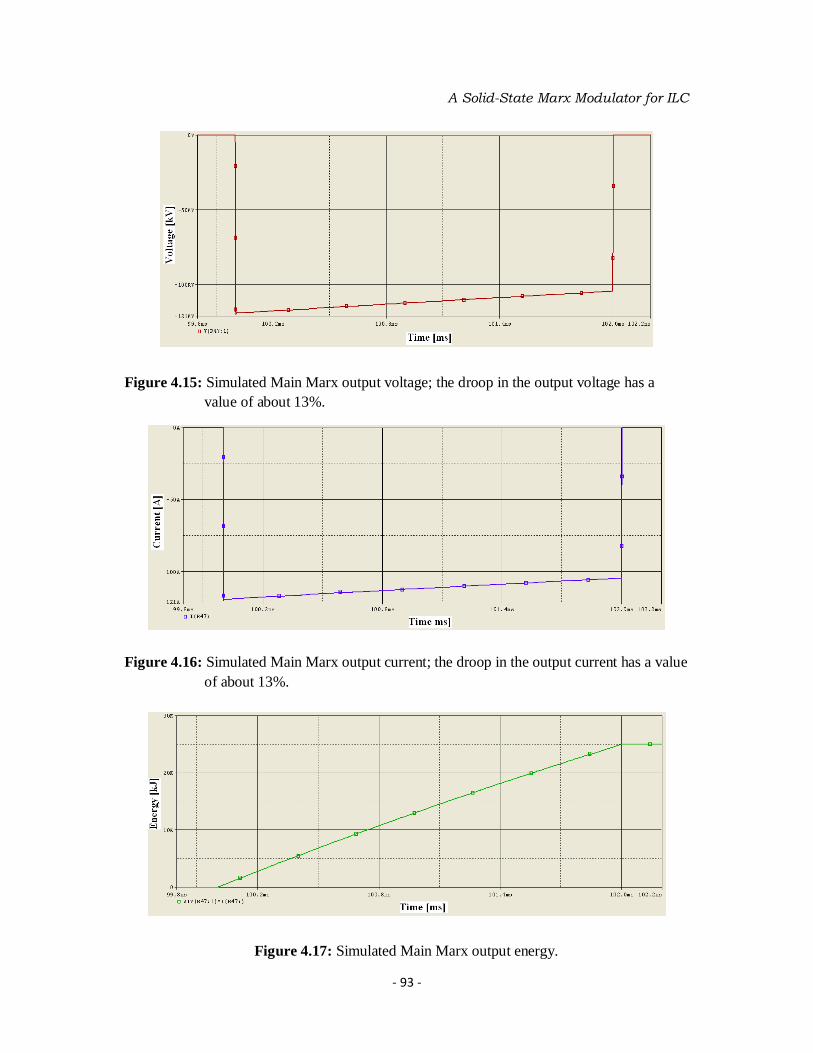
416 Simulated Main Marx output current the droop in the output current has a value of about 13
93
417 Simulated Main Marx output energy 93
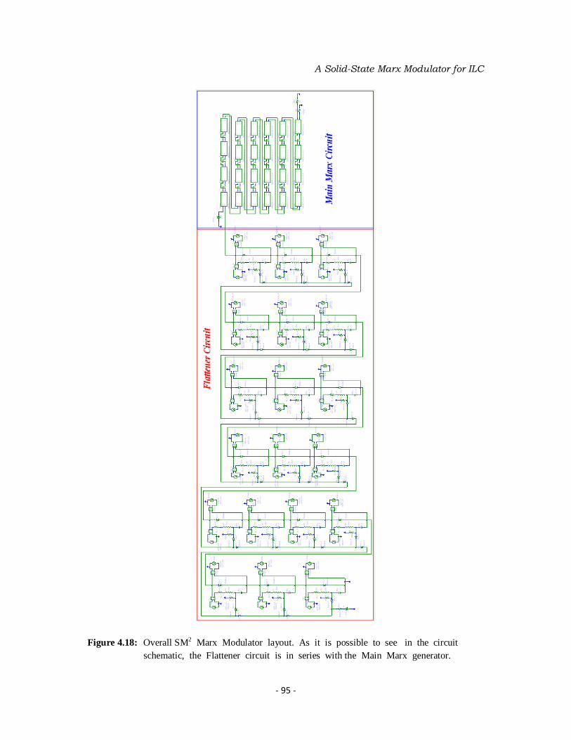
418 Overall SM2 Marx Modulator layout As it is possible to see in the circuit schematic the Flattener circuit is in series with the Main Marx generator
95
419 Full SM2 Modulator conceptual design where STS is the Switching Trigger System for the SM2 modulator MM is the SM2 Main Marx modulator the MMDS is the Main Marx Driving System FDS is the Flattener Driving System and the KEDOSS is the Klystron Energy Droop Out Safety System PS is the SM2 DCDC switching power supply
96
420 Sequence of the trigger signals necessary to operate the Flattener charging switches 97
421 Pulse width of the trigger signals necessary to operate the Flattener discharging switches
97
422 Simulated Flattener output voltage 98
423 Simulated voltage (a) and current (b) droop as a function of number of cell that failed in the SM2 modulator
99
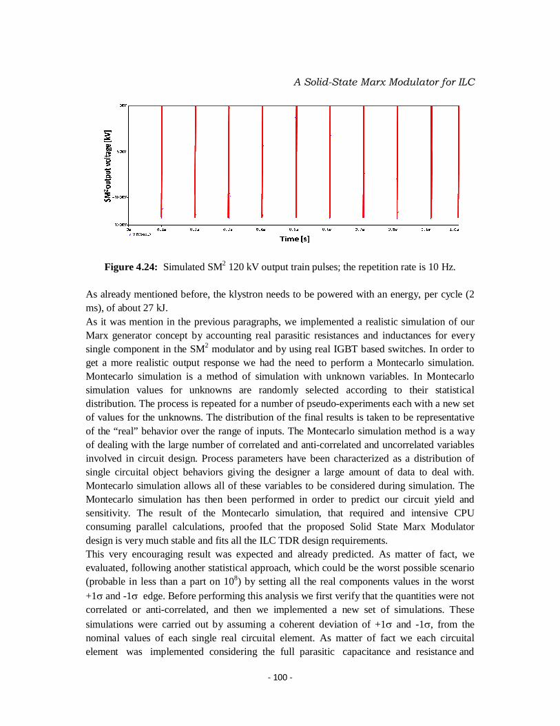
424 Simulated SM2 120 kV output train pulses the repetition rate is 10 Hz 100
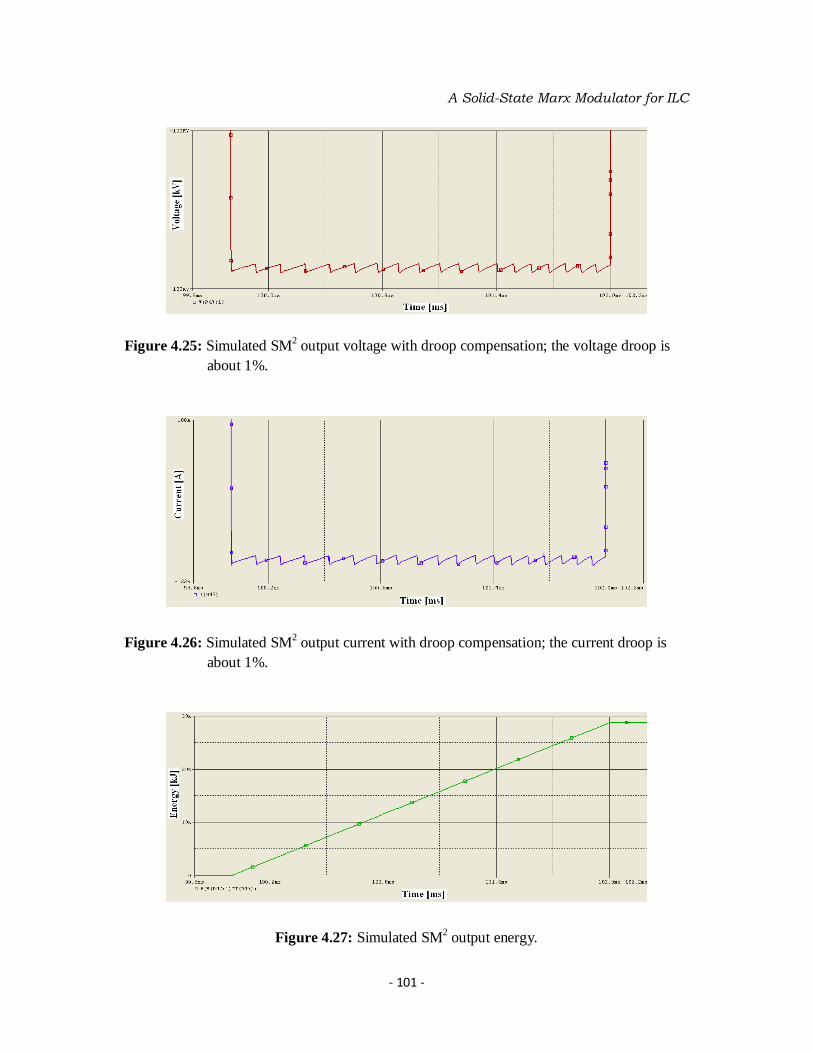
425 Simulated SM2 output voltage with droop compensation the voltage droop is about 1
101
426 Simulated SM2 output voltage with droop compensation the voltage droop is about 1
101
427 Simulated SM2 output energy 101
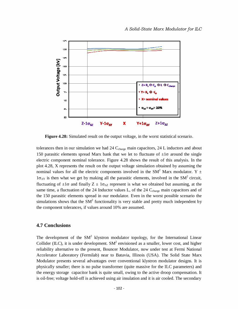
428 Simulated result on the output voltage in the worst statistical scenario 102
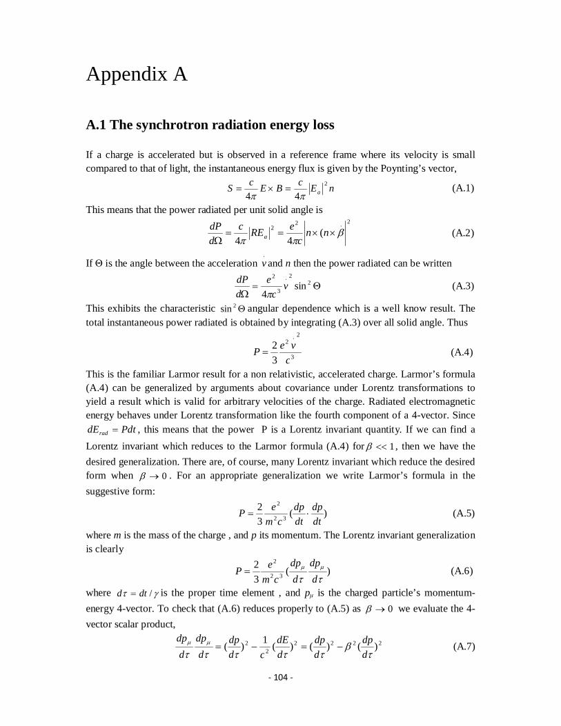
A1 Angular distribution of synchrotron radiation 107
xiv
ldquoCi sono soltanto due possibili conclusioni Se il risultato conferma le ipotesi allora hai appena fatto una misura Se il risultato egrave contrario alle ipotesi allora hai fatto una scopertardquo
Enrico Fermi
ldquoIf we take everything into account not only what the ancient knew but all of what we know today that they didnrsquot know then I think we must frankly admit that we do not knowrdquo
Richard P Feynman
- 1 -
Chapter 1
Physics motivations for the International Linear Collider The International Linear Collider (ILC) is the next large project in accelerator based particle physics It is complementary to the Large Hadron Collider (LHC) in many aspects Measurements from both machines together will finally shed light onto the known deficiencies of the Standard Model of particle physics and allow to unveil a possible underlying more fundamental theory Here the possibilities of the ILC will be discussed with special emphasis on the Higgs sector and on topics with a strong connection to cosmological questions like extra dimensions or dark matter candidates
11 Introduction The Standard Model of particle physics (SM) provides a unified and precise description of all known subatomic phenomena It is consistent at the quantum loop level and it covers distances down to 10minus18 m and times from today until 10minus10 s after the Big Bang Despite its success the SM has some deficiencies which indicate that it is only the effective low energy limit of a more fundamental theory These deficiencies comprise the absence of experimental evidence for the Higgs particle its number of free parameters and their values finendashtuning and stability problems above energies of about 1 TeV and last but not least its ignorance of gravity Furthermore the SM contains no particle which could account for the cold dark matter observed in the universe There are good reasons to expect phenomena beyond the SM at the TeV scale ie in the reach of the immediate generation of new accelerators Any new physics which solves the hierarchy problem between the electroweak and the Planck scale needs to be close to the former Experimental hints arise from the fits to electroweak precision data which require either a Higgs boson mass below 250 GeVc2 or something else which causes similar loop corrections Furthermore most cold dark matter scenarios based on the hypothesis of a weakly interacting massive particle favour masses of about 100 GeVc2 If there are new particles ldquoaround the cornerrdquo the LHC is likely to discover them The ultimate goal however is not only to discover new particles but to measure their properties and interaction with high precision in order to pin down the underlying theory and to determine its parameters In the unlikely case that the LHC will not find any new particles the task of the ILC would be to measure the SM parameters with even higher precision than before [56] in order to find out what is wrong with today fits that point to a light Higgs and new physics at the TeV scale In any case an electron position collider will provide an invaluable tool complementary to the LHC
- 2 -
Physics motivations for the International Linear Collider
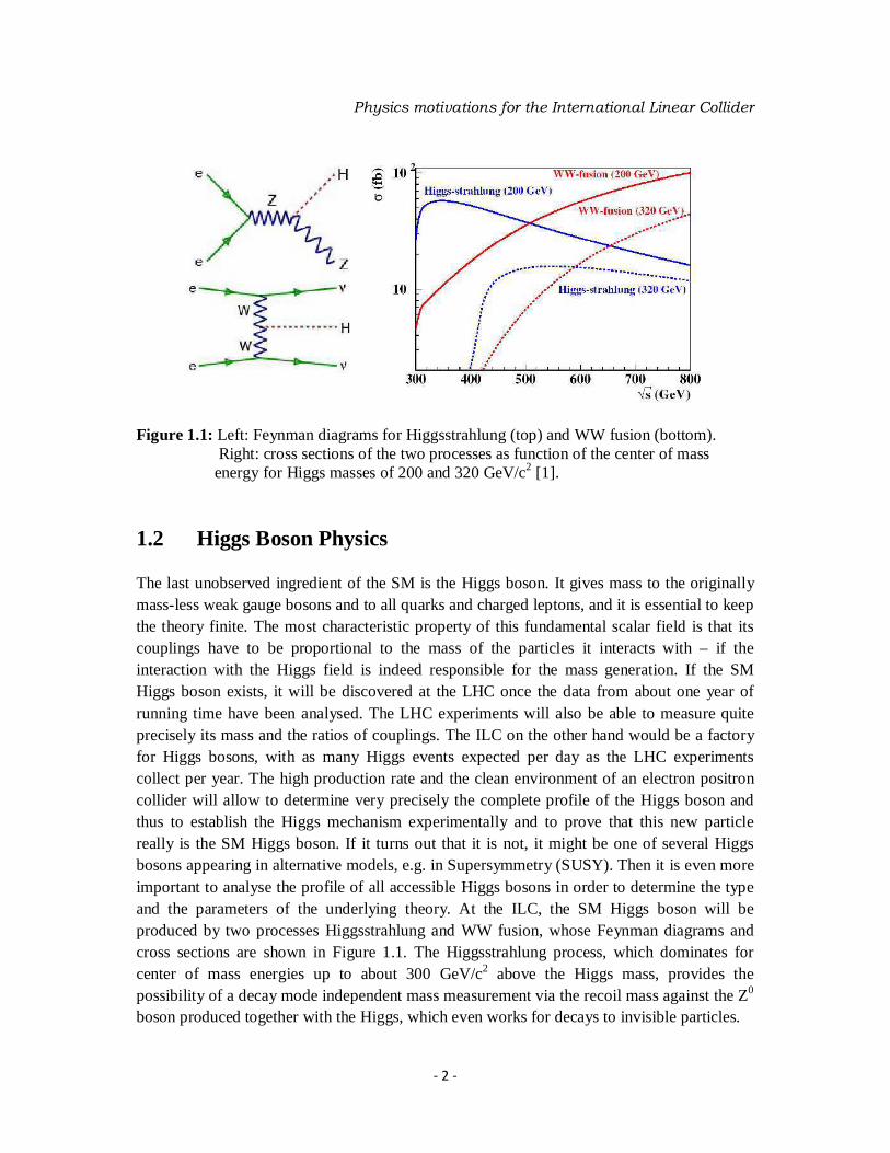
Figure 11 Left Feynman diagrams for Higgsstrahlung (top) and WW fusion (bottom) Right cross sections of the two processes as function of the center of mass energy for Higgs masses of 200 and 320 GeVc2 [1]
12 Higgs Boson Physics The last unobserved ingredient of the SM is the Higgs boson It gives mass to the originally mass-less weak gauge bosons and to all quarks and charged leptons and it is essential to keep the theory finite The most characteristic property of this fundamental scalar field is that its couplings have to be proportional to the mass of the particles it interacts with ndash if the interaction with the Higgs field is indeed responsible for the mass generation If the SM Higgs boson exists it will be discovered at the LHC once the data from about one year of running time have been analysed The LHC experiments will also be able to measure quite precisely its mass and the ratios of couplings The ILC on the other hand would be a factory for Higgs bosons with as many Higgs events expected per day as the LHC experiments collect per year The high production rate and the clean environment of an electron positron collider will allow to determine very precisely the complete profile of the Higgs boson and thus to establish the Higgs mechanism experimentally and to prove that this new particle really is the SM Higgs boson If it turns out that it is not it might be one of several Higgs bosons appearing in alternative models eg in Supersymmetry (SUSY) Then it is even more important to analyse the profile of all accessible Higgs bosons in order to determine the type and the parameters of the underlying theory At the ILC the SM Higgs boson will be produced by two processes Higgsstrahlung and WW fusion whose Feynman diagrams and cross sections are shown in Figure 11 The Higgsstrahlung process which dominates for center of mass energies up to about 300 GeVc2 above the Higgs mass provides the possibility of a decay mode independent mass measurement via the recoil mass against the Z0 boson produced together with the Higgs which even works for decays to invisible particles
- 3 -
Physics motivations for the International Linear Collider
With the detectors planned for the ILC precisions below 01 are achievable over the mass
range favoured by the SM The WW fusion process is a unique tool for determining the total
width of the Higgs boson even for low Higgs masses ie mH lt 200 GeVc2 by measuring the
total WW fusion cross section and the branching ration BR (H WW) At high masses the
Higgs is so broad that its width can be determined directly from its line-shape The total
width then gives access to all couplings via measuring the branching fractions Figure 12
shows the expected precision for the different Higgs branching ratios Especially
disentangling decays to and gg is challenging and requires an excellent vertex
detector The only coupling not accessible in decays is the top Higgs Yukawa coupling gt due
to the high mass of the top quark At the ILC alone one would need to collect 1000 fb-1 at
800 GeVc2 to produce enough e+e- rarr H events to reach a precision of 5 to 10 for gt
A more elegant way to extract gtt H would be to combine the rate measurement of ggrarr
H (with the Higgs decaying further to or W+W-) from the LHC which is proportional to
gt2gb
2W with the absolute measurements of gb and gW from the ILC The mass of the top
quark is one of the most important SM parameters in order to check the overall consistency of
the Higgs mechanism With a scan of the production threshold the top mass can be measured
at the ILC to 50divide100 MeV and its width to 3divide5 The ultimate proof of the Higgs
mechanism is the measurement of the Higgs self coupling λ which allows to map the Higgs
potential and check the relation between λ the Higgs mass and its vacuum expectation value
λ= mH22v2 This needs Higgsstrahlung events where the Higgs itself radiates off a second
Higgs boson which leads to 6-fermion final states including 6-jet final states These require
an excellent jet energy resolution much superior to for example the LEP detectors Once all
Higgs parameters are measured a global fit to all Higgs properties will answer the question if
it really is the SM Higgs boson - or for example a supersymmetric one - even if no other new
particle should be observed at the LHC Even if other particles will have been already
discovered a careful analysis of the Higgs sector is essential to unveil the model beneath the
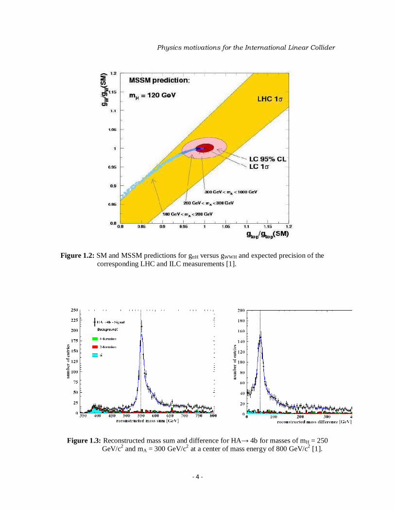
new phenomena and to determine its parameters Figure 12 shows the SM and some MSSM
expectations in the gt-gW plane and the precisions achievable at LHC and at ILC If
Supersymmetry is realised in nature there will be at least five physical Higgs bosons two
CP-even bosons h and H similar to the SM one a neutral CP-odd boson A and two charged
Higgs bosons Hplusmn In contrast to the SM case the Higgs masses are not free parameters but
depend in on other SUSY and SM parameters
- 4 -
Physics motivations for the International Linear Collider
Figure 12 SM and MSSM predictions for gttH versus gWWH and expected precision of the corresponding LHC and ILC measurements [1]
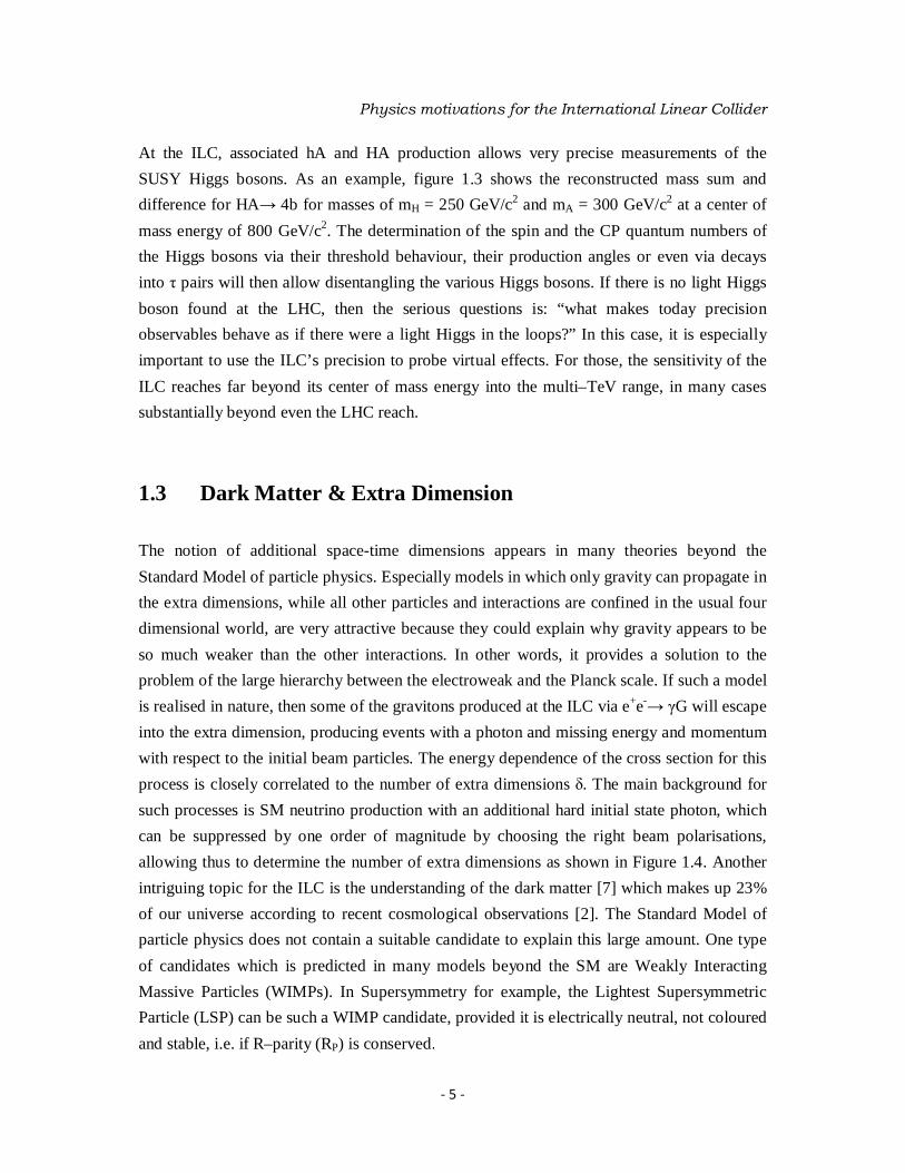
Figure 13 Reconstructed mass sum and difference for HArarr 4b for masses of mH = 250 GeVc2 and mA = 300 GeVc2 at a center of mass energy of 800 GeVc2 [1]
- 5 -
Physics motivations for the International Linear Collider At the ILC associated hA and HA production allows very precise measurements of the
SUSY Higgs bosons As an example figure 13 shows the reconstructed mass sum and
difference for HArarr 4b for masses of mH = 250 GeVc2 and mA = 300 GeVc2 at a center of
mass energy of 800 GeVc2 The determination of the spin and the CP quantum numbers of
the Higgs bosons via their threshold behaviour their production angles or even via decays
into τ pairs will then allow disentangling the various Higgs bosons If there is no light Higgs
boson found at the LHC then the serious questions is ldquowhat makes today precision
observables behave as if there were a light Higgs in the loopsrdquo In this case it is especially
important to use the ILCrsquos precision to probe virtual effects For those the sensitivity of the
ILC reaches far beyond its center of mass energy into the multindashTeV range in many cases
substantially beyond even the LHC reach
13 Dark Matter amp Extra Dimension
The notion of additional space-time dimensions appears in many theories beyond the
Standard Model of particle physics Especially models in which only gravity can propagate in
the extra dimensions while all other particles and interactions are confined in the usual four
dimensional world are very attractive because they could explain why gravity appears to be
so much weaker than the other interactions In other words it provides a solution to the
problem of the large hierarchy between the electroweak and the Planck scale If such a model
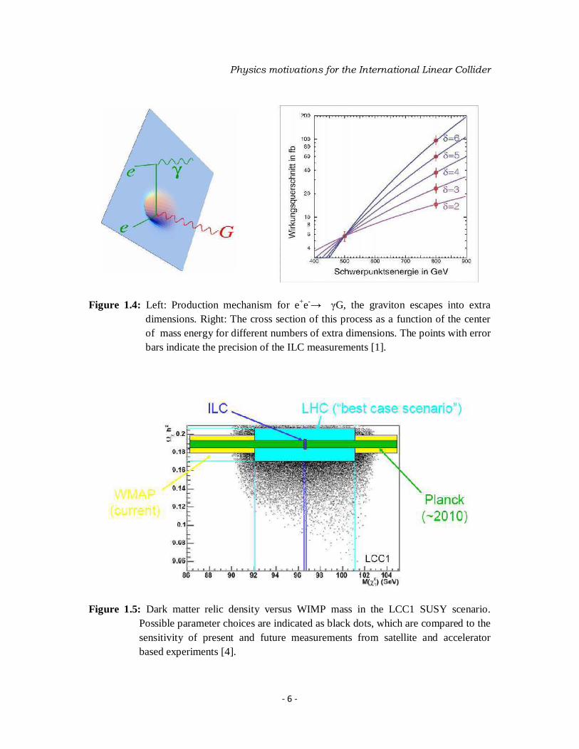
is realised in nature then some of the gravitons produced at the ILC via e+e-rarr γG will escape
into the extra dimension producing events with a photon and missing energy and momentum
with respect to the initial beam particles The energy dependence of the cross section for this
process is closely correlated to the number of extra dimensions δ The main background for
such processes is SM neutrino production with an additional hard initial state photon which
can be suppressed by one order of magnitude by choosing the right beam polarisations
allowing thus to determine the number of extra dimensions as shown in Figure 14 Another
intriguing topic for the ILC is the understanding of the dark matter [7] which makes up 23
of our universe according to recent cosmological observations [2] The Standard Model of
particle physics does not contain a suitable candidate to explain this large amount One type
of candidates which is predicted in many models beyond the SM are Weakly Interacting
Massive Particles (WIMPs) In Supersymmetry for example the Lightest Supersymmetric
Particle (LSP) can be such a WIMP candidate provided it is electrically neutral not coloured
and stable ie if Rndashparity (RP) is conserved
- 6 -
Physics motivations for the International Linear Collider
Figure 14 Left Production mechanism for e+e-rarr γG the graviton escapes into extra dimensions Right The cross section of this process as a function of the center of mass energy for different numbers of extra dimensions The points with error bars indicate the precision of the ILC measurements [1]
Figure 15 Dark matter relic density versus WIMP mass in the LCC1 SUSY scenario Possible parameter choices are indicated as black dots which are compared to the sensitivity of present and future measurements from satellite and accelerator based experiments [4]
- 7 -
Physics motivations for the International Linear Collider The lightest CP-even Higgs h for example must have a mass of less than about 135 GeVc2
Despite its large center of mass energy there are regions in the SUSY parameter space where
the LHC can see only one of the Higgs bosons depending on the parameters of the Higgs
sector for example in maximal mixing scenario at intermediate values of tan β In these
cases the additional precision information from the ILC will be especially important In
many SUSY scenarios the lightest neutralino plays this role which would be discovered at
the LHC The observation and even the mass measurement alone however do not answer the
question whether the LSP accounts for the dark matter in the universe This can only be
clarified when all relevant parameters of the model are determined so that the cross section
for all reactions of the WIMPs with themselves andor other particles and thus the relic
density can be calculated This is illustrated in Figure 15 which shows the calculated relic
density as a function of the mass of the lightest neutralino in the so called LCC1 scenario
The yellow band shows the current knowledge of the relic density from the WMAP
experiment which is expected to be improved significantly by the Planck satellite in the
future (green band) The scattered points result from a scan over the free parameters of this
scenario which can for the same LSP mass yield a large variation in the relic density The
light blue and dark blue boxes indicate the precision of the measurements at the LHC and
ILC respectively It is evident that only the precision of the ILC can match in an appropriate
way the precision of the cosmological observations
Another unique opportunity for dark matter searches at the ILC opens up independently from
specific models By only assuming that WIMPs annihilate into SM particles one can use the
observed relic density and crossing symmetries to calculate an expected rate for WIMP pair
production via e+e- rarr χχ The predicted rates [3] show that such events could be observed at
the ILC by the detection of an additional hard initial state radiation photon however further
more detailed studies are needed
- 8 -
Chapter 2
The ILC Accelerator Design In the past century physicists have explored smaller and smaller scales cataloguing and
understanding the fundamental components of the universe trying to explain the origin of
mass and probing the theory of extra dimensions And in recent years experiments and
observations have pointed to evidence that we can only account for a surprising five percent
of the universe The International Linear Collider (ILC) is a proposed linear particle
accelerator consisting of two linear accelerators that face each other (Figure 21) ILC will
hurl some 10 billion electrons and their anti-particles positrons toward each other at nearly
the speed of light Superconducting accelerator cavities operating at temperatures near
absolute zero give the particles more and more energy until they smash in a blazing crossfire
at the centre of the machine Stretching approximately 31 kilometers in length the beams
collide 14000 times every second at extremely high energies 500 GeV Each collision will
create an array of new particles that could answer some of the most fundamental questions of
all time The current baseline design allows for an upgrade to a 50-kilometre 1 trillion-
electron-volt (TeV) machine during the second stage of the project ILC would collide
electrons with positrons The ILC is based on 13 GHz superconducting RF cavities operating
at a nominal gradient of 35 MeVm The collider operates at a repetition rate of 5divide10 Hz The
site length is 31 km for center of mass energy of 500 GeV the site would have to be extended
to reach 1 TeV The International Linear Colliderrsquos (ILC) most important requirements are
bull an initial center-of-mass (cms) energy up to 500 GeV with the ability to upgrade to 1
TeV
bull an integrated luminosity in the first four years of 500 fb-1 at 500 GeV cms or
equivalent at lower energies
bull the ability to scan in energy between 200 and 500 GeV cms
The installed RF system is capable of accelerating beams for collisions up to center of mass
energy of 500 GeV The design peak luminosity of 2middot1034 cm-2 s-1 at 500 GeV and a collider
availability of 75 should enable to the delivery a total integrated luminosity of about 500
fb-1 in the first four years of physics operations assuming an annual physics run of 9 months
and a gradual ramp up of luminosity over the four years
- 9 -
The ILC Accelerator Design
Figure 21 A schematic layout of the International Linear Collider
Figure 22 Cutaway view of the linac dual-tunnel configuration On the left you can see the
Main Linac tunnel on the right the service tunnel hosting the klystrons the klystron modulators and switching power supplies
- 10 -
The ILC Accelerator Design
Figura 23 Schematic view of the polarized Electron Source
The energy flexibility has been a consideration throughout the design and essential items to
facilitate a future upgrade to 1 TeV such as the length of the beam delivery system and the
power rating of the main beam dumps have been incorporated The beams are prepared in
low energy damping rings that operate at 5 GeV and are 67 km in circumference They are
then accelerated in the main linacs which are around 11 km per side Finally they are focused
down to very small spot sizes at the collision point with a beam delivery system that is about
22 km per side To obtain a peak luminosity of 2middot1034 cm-2 s-1 the collider requires
approximately 230 MW of electrical power
21 Electron and Positron Sources
The ILC polarized electron source (Figure 23) must produce the required train of polarized
electron bunches and transport them to the Damping Ring The nominal train is 2625
bunches of 201010 electrons at 5 Hz with polarization greater than 80 (Table 21) The
beam is produced by a laser illuminating a photocathode in a DC gun Two independent laser
and gun systems provide redundancy Normal-conducting structures are used for bunching
and pre-acceleration to 76 MeV after which the beam is accelerated to 5 GeV in a
superconducting linac Before injection into the damping ring superconducting solenoids
rotate the spin vector into the vertical and a separate superconducting RF structure is used for
energy compression
- 11 -
The ILC Accelerator Design
Table 21 Electrons Source System parameters
Table 22 Nominal Positron Source parameters A third polarized electron source (500 MeV) drives the Positron Keep Alive Source (KAS) Polarization is not required in the baseline but will be required for either the e- - e- or γ ndash γ options The SLC polarized electron source already meets the requirements for polarization charge and lifetime The primary challenge for the ILC source is the long bunch train which demands a laser system beyond that used at any existing accelerator and normal conducting structures which can handle high RF power Both RampD developments are considered manageable In other hand ILC Positron Source uses photo-production to generate positrons (Figure 24)
- 12 -
The ILC Accelerator Design
Figura 24 Overall layout of the Positron Source
The electron main linac beam passes through a long helical undulator to generate a multi-MeV photon beam which then strikes a thin metal target to generate positrons in an electromagnetic shower The positrons are captured accelerated separated from the shower constituents and unused photon beam and then are transported to the Damping Ring Although the baseline design only requires unpolarized positrons the positron beam produced by the baseline source has a polarization of ~30 and beam-line space has been reserved for an eventual upgrade to ~60 polarization (Table 22) The positron source must perform three critical functions
bull generate a high power multi-MeV photon production drive beam in a suitable short period high K-value helical undulator
bull produce the needed positron bunches in a metal target that can reliably deal with the beam power and induced radioactivity
bull capture and transport the positron bunch to the ILC Damping Rings with minimal beam loss In addition the Positron Source requires sufficient instrumentation diagnostics and feedback (feed-forward) systems to ensure optimal operation of the source and ILC
22 Service Rings
221 Damping Rings The ILC damping rings include one electron and one positron ring each 67 km long operating at beam energy of 5 GeV The two rings are housed in a single tunnel near the center of the site with one ring positioned directly above the other The damping rings must perform three critical functions
- 13 -
The ILC Accelerator Design
Table 23 Positron Damping Ring parameters the Electron Damping Ring is identical except for a smaller injected emittance
bull Accept e- and e+ beams with large transverse and longitudinal emittances and produce
the low-emittance beams required for luminosity production
bull Damp incoming beam jitter (transverse and longitudinal) and provide highly stable
beams for downstream systems
bull Delay bunches from the source to allow feed-forward systems to compensate for
pulse- to-pulse variations in parameters such as the bunch charge
- 14 -
The ILC Accelerator Design
Figure 25 Dynamic aperture of ILC Damping Ring (without field or alignment error) for relative momentum errors of -1 0 and 1 at x = 44 m and y = 18 m The tick green line represents the size of the injected positron beam
Figure 26 Schematic of RTML
- 15 -
The ILC Accelerator Design
Table 24 Basic beam parameters of the RTML The damping ring system includes the injection and extraction systems which includes
sections of transport lines matching to the sources (upstream of the damping rings) and the
RTML system (downstream of the damping rings)
222 Ring to Main Linac
The ILC Ring to Main Linac (RTML) is responsible for transporting and matching the beam
from the Damping Ring to the entrance of the Main Linac
The RTML must perform several critical functions
bull transport of the electron and positron beams from the damping rings at the center of
the ILC accelerator complex to the upstream ends of their respective linacs
(ldquogeometry matching)
bull collimation of the beam halo generated in the damping ring
bull rotation of the spin polarization vector from the vertical to any arbitrary angle
required at the IP
bull compression of the long Damping Ring bunch length by a factor of 30 ~ 45 to provide
the short bunches required by the Main Linac and the IP
- 16 -
The ILC Accelerator Design
Table 25 Nominal beam parameters in the ILC Main Linac
23 Main Linacs
The two main linacs accelerate the electron and positron beams from their injected energy of
15 GeV to the final beam energy of 250 GeV over a combined length of 23 km This must be
accomplished while preserving the small bunch emittances which requires precise orbit
control based on data from high resolution beam position monitors The linacs utilize L-band
(13 GHz) superconducting technology with nine-cell standing-wave niobium cavities
operating at an average gradient of 315 MVm in a 2K super-fluid helium bath The choice
of operating frequency is a balance between the high cavity cost due to size at lower
frequency and the lower sustainable gradient due to increased surface resistivity at higher
frequency The accelerator gradient is somewhat higher than that typically achievable today
and assumes that further progress will be made during the next few years in the aggressive
program that is being pursued to improve cavity performance The Table 25 lists the key
beam parameters in the main linac The rms bunch length remains constant along the linacs
while the bunch fractional energy spread decreases roughly as E0E where E is the beam
energy and E0 is the initial main linac beam energy Bunches are phased 5deg off-crest to
minimize their energy spread No BNS energy spread is included to suppress resonant head-
to-tail bunch trajectory growth as the short-range wake-field is fairly weak For this same
reason the focusing strength of the quadrupole lattice in the linacs is kept fairly weak to
reduce emittance growth from quadrupole misalignments
- 17 -
The ILC Accelerator Design
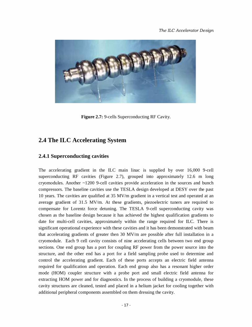
Figure 27 9-cells Superconducting RF Cavity
24 The ILC Accelerating System 241 Superconducting cavities The accelerating gradient in the ILC main linac is supplied by over 16000 9-cell superconducting RF cavities (Figure 27) grouped into approximately 126 m long cryomodules Another ~1200 9-cell cavities provide acceleration in the sources and bunch compressors The baseline cavities use the TESLA design developed at DESY over the past 10 years The cavities are qualified at 35 MVm gradient in a vertical test and operated at an average gradient of 315 MVm At these gradients piezoelectric tuners are required to compensate for Lorentz force detuning The TESLA 9-cell superconducting cavity was chosen as the baseline design because it has achieved the highest qualification gradients to date for multi-cell cavities approximately within the range required for ILC There is significant operational experience with these cavities and it has been demonstrated with beam that accelerating gradients of greater then 30 MVm are possible after full installation in a cryomodule Each 9 cell cavity consists of nine accelerating cells between two end group sections One end group has a port for coupling RF power from the power source into the structure and the other end has a port for a field sampling probe used to determine and control the accelerating gradient Each of these ports accepts an electric field antenna required for qualification and operation Each end group also has a resonant higher order mode (HOM) coupler structure with a probe port and small electric field antenna for extracting HOM power and for diagnostics In the process of building a cryomodule these cavity structures are cleaned tested and placed in a helium jacket for cooling together with additional peripheral components assembled on them dressing the cavity
- 18 -
The ILC Accelerator Design
Table 26 ILC 9-cell Superconducting Cavity layout parameters
Table 27 Properties of high-RRR (residual resistivity ratio) Niobium suitable for use in ILC Cavities A dressed cavity contains one 9-cell niobium cavity structure coarse and fine tuners for adjusting the frequency of the structure magnetic shielding material to minimize the cavity losses a variable coupling high power input antenna for powering the cavity an electric field sampling antenna and two higher order mode electric field antennas Nine of these dressed cavities are usually connected into a string and are a subcomponent of a superconducting cryomodule The basic design parameters for this cavity are listed in Table 26 and 27
- 19 -
The ILC Accelerator Design
Figure 28 RF unit diagram showing the basic waveguide distribution layout between the klystron and 26 cavities in three cryomodules
242 RF distribution system The main linacs are composed of RF units whose layout is illustrated in Figure 28 and whose parameters are listed in Table 28 Each unit has a stand-alone RF source that powers three contiguous cryomodules containing a total of 26 cavities (with 9 8 and 9 cavities in each cryomodule respectively) The RF source includes a high-voltage modulator a 10 MW klystron and a waveguide system that distributes the RF power to the cavities It also includes the low-level RF (LLRF) system to regulate the cavity field levels interlock systems to protect the source components and the power supplies and support electronics associated with the operation of the source To facilitate maintenance and limit radiation exposure the RF source is housed mainly in a separate service tunnel that runs parallel to the beam tunnel The modulator is a conventional pulse-transformer type with a bouncer circuit to compensate the voltage droop that occurs in the main storage capacitor during the pulse The modulator produces 120 kV 130 A 16 ms 5-10 Hz pulses with an efficiency of 83 including the charging supply and rise time losses These high voltage pulses power a multi-beam klystron (MBK) that amplifies ~ 100 W 16 ms RF pulses from the LLRF system up to 10 MW This klystron has higher power and improved efficiency (65 goal) relative to commercial 5 MW tubes (40-45) The dual outputs of the klystron feed into two waveguides each carrying half the power which runs roughly 11 m to the linac through a penetration between the service tunnel and the main tunnel High-power in-line attenuators allow more power to be sent through one arm than the other to accommodate different average gradient capabilities in the sets of cavities they feed The penetration emerges approximately at the center of the middle cryomodule of the unit Here a hybrid splitter divides the power in each waveguide with a 49 ratio (-512 dB)
- 20 -
The ILC Accelerator Design
Table 28 RF Unit parameters
The lower power output of each splitter feeds half the center cryomodule and the higher
power output is carried approximately 6 m to one of the outer cryomodules (see Figure 28)
Along each cryomodule RF power is equally distributed among the cavities in a linear
waveguide system passing through a series of hybrid-style 4-port tap-offs These tap-offs
couple the appropriate sequential fraction (18 17 12 or 141312) of the power
remaining in the line to all but the last cavity which is directly fed the remainder The
nominal power required in each cavity is 2937 kW Between the tap-offs the remainder of
the 1326 m coupler spacing is filled with modified straight waveguide sections whose width
is symmetrically tapered with 14-wave transformer matching steps varying the guide
wavelength to roughly yield the proper inter-cavity phasing Between each tap-off output and
its associated cavity coupler are a circulator a three-stub tuner and a diagnostic directional
coupler (see Figure 29) The three-stub tuner allows fine adjustment of both cavity phase and
external coupling The circulator with a load on its third port (thus technically an isolator)
absorbs RF power reflected from the standing-wave cavity during filling and emitted during
discharge It provides protection to the klystron and isolation between cavities A couple of
E-plane waveguide U-bends are also needed to keep the system compact and feed into the
downward pointed coupler flange and a short semi-flexible section is included to relieve
stress and ease alignment tolerances
- 21 -
The ILC Accelerator Design
Figure 29 Waveguide circuit from tap-off hybrid to coupler input showing the various components (except for the directional coupler)
Figure 210 Toshiba 3736 Multi-Beam Klystron
243 Klystron
The accelerating gradient for the ILC main linacs is supplied by superconducting 13 GHz cavities powered by 560 10 MW RF stations each with a modulator klystron and RF distribution system Another 86 identical klystronmodulator systems are used in the e+ and e- Sources and RTML bunch compressors The damping ring RF power is supplied by 650 MHz superconducting cavities powered by 12 MW CW klystrons These are fed from a DC charging supply and do not have modulators There are also a few special purpose S-band RF stations for instrumentation and a 39 GHz RF station to power the crab cavities near the Interaction Point
- 22 -
The ILC Accelerator Design
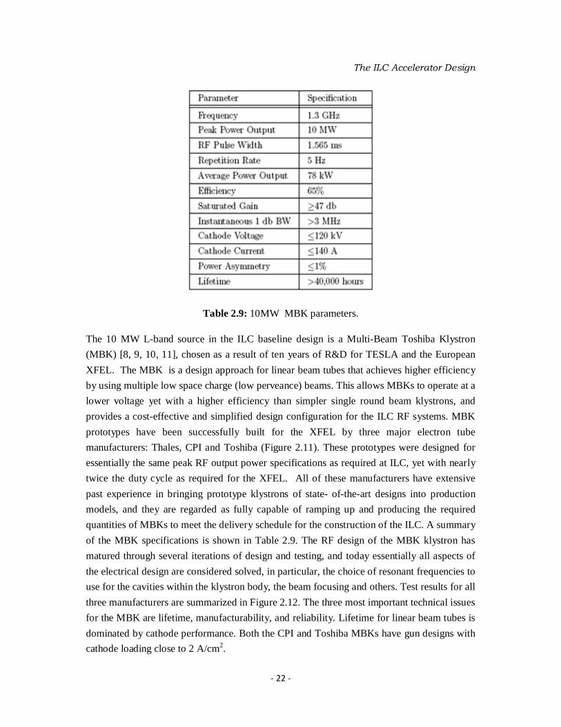
Table 29 10MW MBK parameters The 10 MW L-band source in the ILC baseline design is a Multi-Beam Toshiba Klystron
(MBK) [8 9 10 11] chosen as a result of ten years of RampD for TESLA and the European
XFEL The MBK is a design approach for linear beam tubes that achieves higher efficiency
by using multiple low space charge (low perveance) beams This allows MBKs to operate at a
lower voltage yet with a higher efficiency than simpler single round beam klystrons and
provides a cost-effective and simplified design configuration for the ILC RF systems MBK
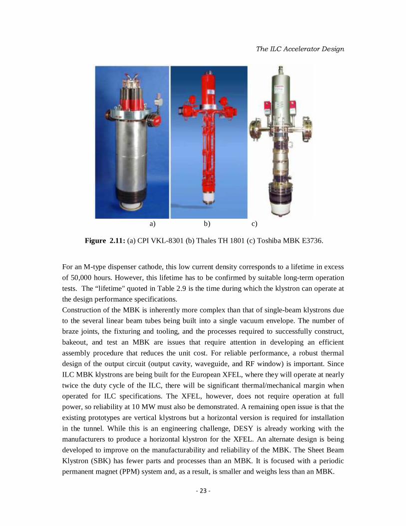
prototypes have been successfully built for the XFEL by three major electron tube
manufacturers Thales CPI and Toshiba (Figure 211) These prototypes were designed for
essentially the same peak RF output power specifications as required at ILC yet with nearly
twice the duty cycle as required for the XFEL All of these manufacturers have extensive
past experience in bringing prototype klystrons of state- of-the-art designs into production
models and they are regarded as fully capable of ramping up and producing the required
quantities of MBKs to meet the delivery schedule for the construction of the ILC A summary
of the MBK specifications is shown in Table 29 The RF design of the MBK klystron has
matured through several iterations of design and testing and today essentially all aspects of
the electrical design are considered solved in particular the choice of resonant frequencies to
use for the cavities within the klystron body the beam focusing and others Test results for all
three manufacturers are summarized in Figure 212 The three most important technical issues
for the MBK are lifetime manufacturability and reliability Lifetime for linear beam tubes is
dominated by cathode performance Both the CPI and Toshiba MBKs have gun designs with
cathode loading close to 2 Acm2
- 23 -
The ILC Accelerator Design
a) b) c)
Figure 211 (a) CPI VKL-8301 (b) Thales TH 1801 (c) Toshiba MBK E3736
For an M-type dispenser cathode this low current density corresponds to a lifetime in excess
of 50000 hours However this lifetime has to be confirmed by suitable long-term operation
tests The ldquolifetime quoted in Table 29 is the time during which the klystron can operate at
the design performance specifications
Construction of the MBK is inherently more complex than that of single-beam klystrons due
to the several linear beam tubes being built into a single vacuum envelope The number of
braze joints the fixturing and tooling and the processes required to successfully construct
bakeout and test an MBK are issues that require attention in developing an efficient
assembly procedure that reduces the unit cost For reliable performance a robust thermal
design of the output circuit (output cavity waveguide and RF window) is important Since
ILC MBK klystrons are being built for the European XFEL where they will operate at nearly
twice the duty cycle of the ILC there will be significant thermalmechanical margin when
operated for ILC specifications The XFEL however does not require operation at full
power so reliability at 10 MW must also be demonstrated A remaining open issue is that the
existing prototypes are vertical klystrons but a horizontal version is required for installation
in the tunnel While this is an engineering challenge DESY is already working with the
manufacturers to produce a horizontal klystron for the XFEL An alternate design is being
developed to improve on the manufacturability and reliability of the MBK The Sheet Beam
Klystron (SBK) has fewer parts and processes than an MBK It is focused with a periodic
permanent magnet (PPM) system and as a result is smaller and weighs less than an MBK
- 24 -
The ILC Accelerator Design
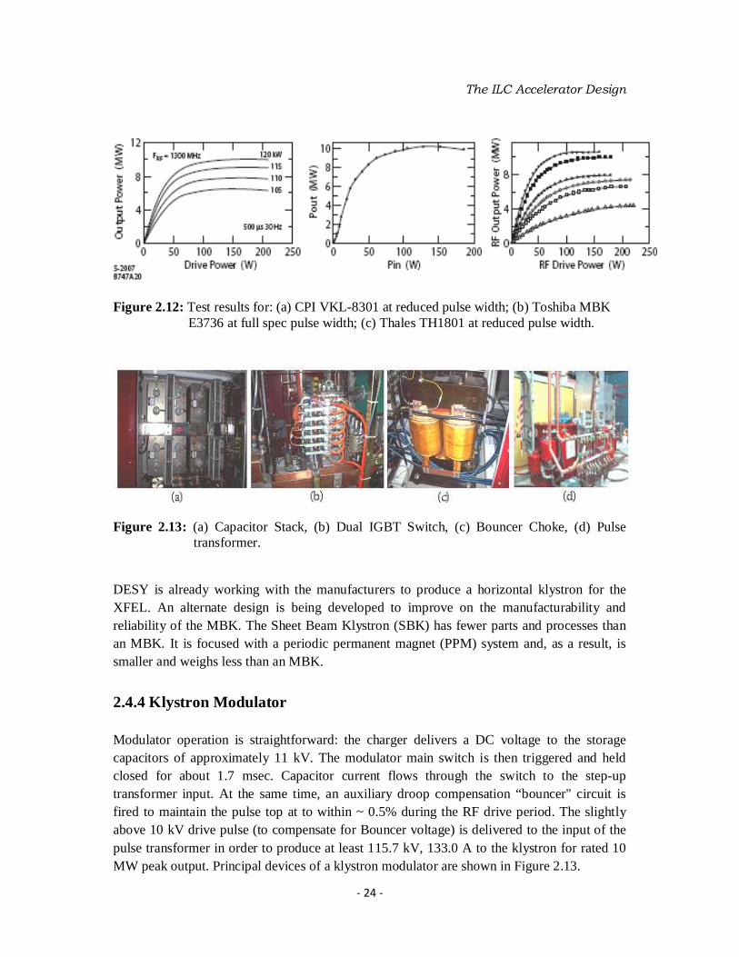
Figure 212 Test results for (a) CPI VKL-8301 at reduced pulse width (b) Toshiba MBK E3736 at full spec pulse width (c) Thales TH1801 at reduced pulse width
Figure 213 (a) Capacitor Stack (b) Dual IGBT Switch (c) Bouncer Choke (d) Pulse
transformer DESY is already working with the manufacturers to produce a horizontal klystron for the XFEL An alternate design is being developed to improve on the manufacturability and reliability of the MBK The Sheet Beam Klystron (SBK) has fewer parts and processes than an MBK It is focused with a periodic permanent magnet (PPM) system and as a result is smaller and weighs less than an MBK
244 Klystron Modulator Modulator operation is straightforward the charger delivers a DC voltage to the storage capacitors of approximately 11 kV The modulator main switch is then triggered and held closed for about 17 msec Capacitor current flows through the switch to the step-up transformer input At the same time an auxiliary droop compensation ldquobouncer circuit is fired to maintain the pulse top at to within ~ 05 during the RF drive period The slightly above 10 kV drive pulse (to compensate for Bouncer voltage) is delivered to the input of the pulse transformer in order to produce at least 1157 kV 1330 A to the klystron for rated 10 MW peak output Principal devices of a klystron modulator are shown in Figure 213
- 25 -
The ILC Accelerator Design
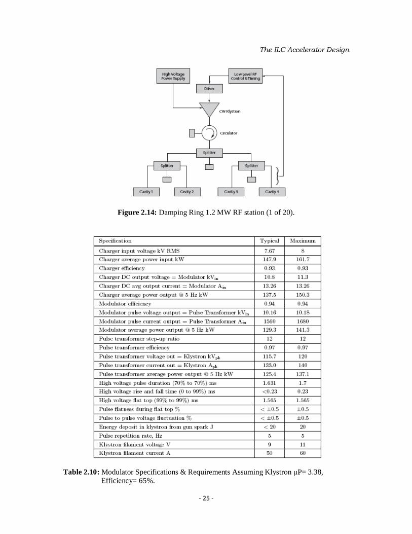
Figure 214 Damping Ring 12 MW RF station (1 of 20)
Table 210 Modulator Specifications amp Requirements Assuming Klystron microP= 338 Efficiency= 65
- 26 -
The ILC Accelerator Design
Figure 215 The overall layout concept for the cryogenic systems The Damping Rings have 650 MHz CW stations using 12 MW peak power klystrons 20 in total for 2 rings Power is supplied from a DC supply of 20 MW delivering 50-75 kV at 17-10 A DC The RF envelope is controlled by the low level RF and timing to maintain stability and clearing gaps as needed The station block diagram is shown in Figure 214 There are no major technical issues with the L-Band modulator as long as the entire system has sufficient overhead (redundancy) to compensate for a failed station To achieve an acceptable availability the linac energy and beam current parameters must be chosen to provide some RF spare stations Redundancy of internal components such as IGBT switches and sectioning of chargers for N+1 redundancy is also important Currently this is only partially implemented in the prototypes The present design which develops the drive pulse at low voltage and high current has larger losses than would be experienced with a higher voltage design This is not a major technical issue but a cost size and weight issue Installation and repair during operations will be more difficult with multi-ton components such as the transformer and main capacitor switch multi-cabinet assembly An alternative modulator design is being investigated to address these issues including the possibility of significant cost reduction The design would reduce the overall footprint and eliminate the step-up transformer and other oil-filled components
245 The cryogenic systems With superconducting equipment throughout the ILC cryogenic systems of extensive size and capacity will be required (Figure 215) Superconducting RF cavities operating at 2 K in the main linacs are the primary accelerating structures in the ILC and comprise the largest cryogenic cooling load Although not as extensive the positron and electron sources damping rings RTML and beam delivery systems include a large number and variety of superconducting RF cavities
- 27 -
The ILC Accelerator Design
Table 211 Superconducting RF modules in the ILC excluding the two 6-cavity energy compressor cryomodules located in the electron and positron LTRs Table 211 summarizes the numbers of various types of superconducting RF modules in the ILC In addition to the RF modules listed in Table 211 there are a variety of superconducting (SC) magnets in the ILC About one third of the 13 GHz cryogenic modules contain SC magnets As part of the positron source the electron linac includes about 150 meters of SC helical undulators in 2 to 4 meter length units The Damping Rings have 8 strings of superconducting wiggler magnets and there are special SC magnets in the sources RTML and beam delivery system Figure 215 illustrates the concept for the cryogenic system arrangement in ILC Ten large cryogenic plants with 2 Kelvin refrigeration cool the main linac RTML and the electron and positron sources Three smaller cryogenic plants with mostly 45 K loads cool the damping rings and beam delivery system The ILC cryogenic systems are defined to include cryogen distribution as well as production Thus components of the cryogenic system include the cryogenic plants distribution and interface boxes transfer lines and non-magnetic non-RF cold tunnel components Although cryomodules SC magnets and production test systems also include significant cryogenics those are not considered in this section of the RDR Main linac cryogenic modules each containing eight (with magnet package) or nine (without magnet package) nine-cell niobium cavities cold helium pipes and thermal shields are the dominant load to be cooled by the cryogenic system The magnet package in one third of the cryomodules includes a superconducting quadrupole and corrector magnets The ILC cryomodule design for the 13 GHz RF is based on the TESLA Test Facility (TTF) type III design which contains all the cryogenic pipe-work inside its vacuum enclosure There are approximately 23 km of 13 GHz cryomodules including main linac RTML and sources Series architecture is mostly used in the cryogenic unit cooling scheme
- 28 -
The ILC Accelerator Design
Figure 216 Cooling scheme of a cryo-string
Like for the TESLA cryogenic concept saturated He II cools RF cavities at 2 K and helium gas cooled shields intercept thermal radiation and thermal conduction at 5 - 8 K and at 40 - 80 K A two-phase line (liquid helium supply and concurrent vapor return) connects to each helium vessel and connects to the major gas return header once per module A small diameter warm-upcool-down line connects the bottoms of the He vessels A subcooled helium supply line connects to the two-phase line via a Joule-Thomson valve once per string (typically 12 modules) The 5 K and 40 K heat intercepts and radiation screens are cooled in series through an entire cryogenic unit of up to 25 km in length For the 2 K cooling of the RF cavities a parallel architecture is implemented with the parallel cooling of cryo-strings resulting in operational flexibility Consequently each cryogenic unit is subdivided into about 14 to 16 cryo-strings each of which corresponds to the 154 meter length elementary block of the cryogenic refrigeration system Figure 216 shows the cooling scheme of a cryo-string which contains 12 cryomodules The cavities are immersed in baths of saturated super-fluid helium gravity filled from a 2 K two phase header Saturated super-fluid helium owes all along the two-phase header for filling the cavities and phase separators located at both ends of the two-phase header The first phase separator is used to stabilize the saturated liquid produced during the final expansion The second phase separator in used to recover the excess of liquid which is vaporized by a heater At the interconnection of each cryomodule the two-phase header is connected to the pumping return line The division of the Main Linac into cryogenic units is driven by various plant size limits and a practical size for the low pressure return pipe A cryogenic plant of 25 kW equivalent 45 K capacity is a practical limit due to industrial production for heat exchanger sizes and over-the-road shipping size restrictions Cryomodule piping pressure drops also start to become rather large with more than 25 km distances Practical plant size and gas return header pressure drop limits are reached with 192 modules in a 16-string cryogenic unit 247 km long
- 29 -
The ILC Accelerator Design
Figure 217 Two-phase helium flow for level and for sloped systems Five cryogenic units divide the main linac conveniently for placing the positron source
undulators at 150 GeV As the ILC site has not yet been selected the cryogenic system
concept must accommodate different configurations of tunnel and civil works The tunnel
may follow the earths curvature or be laser-straight with a maximum slope of up to 06 creating large elevation differences To avoid harmful instabilities all fluid should ideally be
transported over large distances in a mono-phase state Local two-phase circulation of
saturated liquid can be tolerated over limited lengths within a controlled range of vapor
quality Figure 217 illustrates two methods of liquid management in the two-phase supply
pipe for main linac cryogenic modules one case for a sloped system and the other for a level system As listed above in Table 210 electron and positron sources each include just over 20
SRF modules containing 13 GHz RF cavities cooled to 2 Kelvin The sources also include
several superconducting magnets as well as about 150 meters of superconducting positron
source undulators These undulators are cooled by one of the cryogenic plants in the electron
linac cryogenic system Damping ring cryogenic loads include 45 K superconducting wigglers 45 K 650 MHz cryomodules associated cryogenic distribution systems and 70 K
thermal shields for all of these Two cryogenic plants serve the damping rings The beam
delivery system has one 39 GHz cryomodule (containing two cavities) on each side of the
interaction point superconducting final focus quadrupoles and other special superconducting magnets spaced several hundred meters from the IR One cryogenic plant serves both sides of
the interaction region
- 30 -
The ILC Accelerator Design
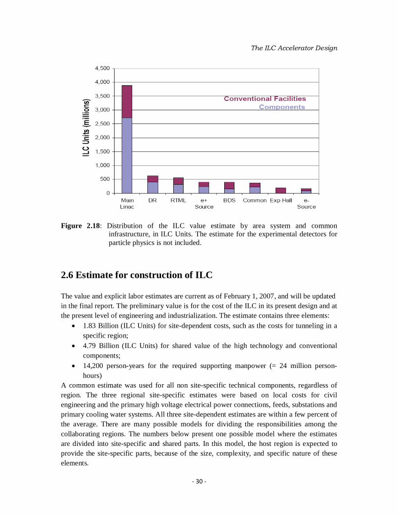
Figure 218 Distribution of the ILC value estimate by area system and common
infrastructure in ILC Units The estimate for the experimental detectors for particle physics is not included
26 Estimate for construction of ILC The value and explicit labor estimates are current as of February 1 2007 and will be updated in the final report The preliminary value is for the cost of the ILC in its present design and at the present level of engineering and industrialization The estimate contains three elements
bull 183 Billion (ILC Units) for site-dependent costs such as the costs for tunneling in a specific region
bull 479 Billion (ILC Units) for shared value of the high technology and conventional components
bull 14200 person-years for the required supporting manpower (= 24 million person-hours)
A common estimate was used for all non site-specific technical components regardless of region The three regional site-specific estimates were based on local costs for civil engineering and the primary high voltage electrical power connections feeds substations and primary cooling water systems All three site-dependent estimates are within a few percent of the average There are many possible models for dividing the responsibilities among the collaborating regions The numbers below present one possible model where the estimates are divided into site-specific and shared parts In this model the host region is expected to provide the site-specific parts because of the size complexity and specific nature of these elements
- 31 -
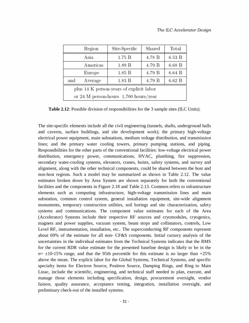
The ILC Accelerator Design
Table 212 Possible division of responsibilities for the 3 sample sites (ILC Units)
The site-specific elements include all the civil engineering (tunnels shafts underground halls and caverns surface buildings and site development work) the primary high-voltage electrical power equipment main substations medium voltage distribution and transmission lines and the primary water cooling towers primary pumping stations and piping Responsibilities for the other parts of the conventional facilities low-voltage electrical power distribution emergency power communications HVAC plumbing fire suppression secondary water-cooling systems elevators cranes hoists safety systems and survey and alignment along with the other technical components could be shared between the host and non-host regions Such a model may be summarized as shown in Table 212 The value estimates broken down by Area System are shown separately for both the conventional facilities and the components in Figure 218 and Table 213 Common refers to infrastructure elements such as computing infrastructure high-voltage transmission lines and main substation common control system general installation equipment site-wide alignment monuments temporary construction utilities soil borings and site characterization safety systems and communications The component value estimates for each of the Area (Accelerator) Systems include their respective RF sources and cryomodules cryogenics magnets and power supplies vacuum system beam stops and collimators controls Low Level RF instrumentation installation etc The superconducting RF components represent about 69 of the estimate for all non- CFampS components Initial cursory analysis of the uncertainties in the individual estimates from the Technical Systems indicates that the RMS for the current RDR value estimate for the presented baseline design is likely to be in the σ= plusmn10-15 range and that the 95th percentile for this estimate is no larger than +25 above the mean The explicit labor for the Global Systems Technical Systems and specific specialty items for Electron Source Positron Source Damping Rings and Ring to Main Linac include the scientific engineering and technical staff needed to plan execute and manage those elements including specification design procurement oversight vendor liaison quality assurance acceptance testing integration installation oversight and preliminary check-out of the installed systems
- 32 -
The ILC Accelerator Design
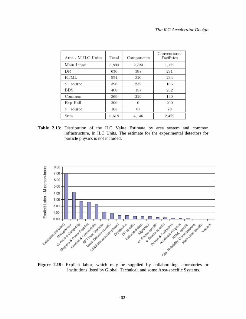
Table 213 Distribution of the ILC Value Estimate by area system and common infrastructure in ILC Units The estimate for the experimental detectors for particle physics is not included
Figure 219 Explicit labor which may be supplied by collaborating laboratories or
institutions listed by Global Technical and some Area-specific Systems
- 33 -
The ILC Accelerator Design
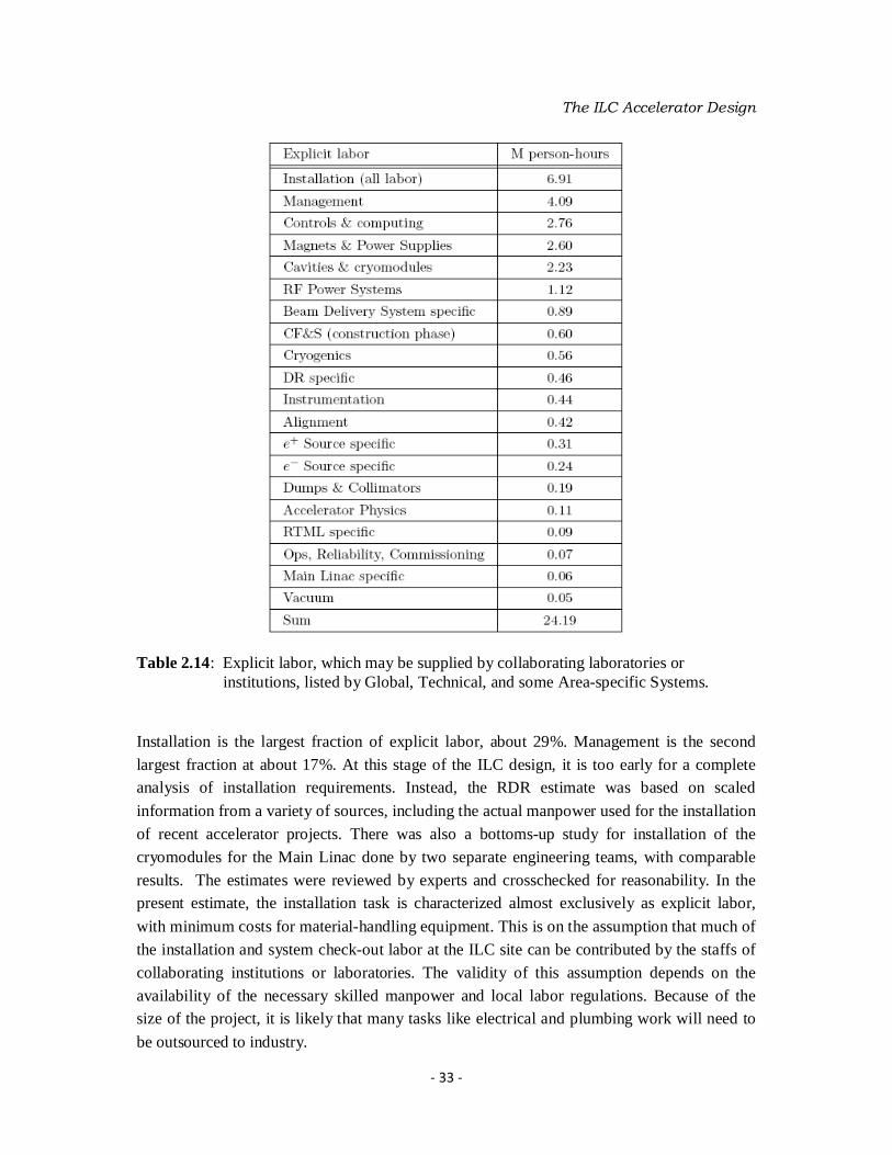
Table 214 Explicit labor which may be supplied by collaborating laboratories or institutions listed by Global Technical and some Area-specific Systems
Installation is the largest fraction of explicit labor about 29 Management is the second
largest fraction at about 17 At this stage of the ILC design it is too early for a complete analysis of installation requirements Instead the RDR estimate was based on scaled
information from a variety of sources including the actual manpower used for the installation
of recent accelerator projects There was also a bottoms-up study for installation of the
cryomodules for the Main Linac done by two separate engineering teams with comparable
results The estimates were reviewed by experts and crosschecked for reasonability In the present estimate the installation task is characterized almost exclusively as explicit labor
with minimum costs for material-handling equipment This is on the assumption that much of
the installation and system check-out labor at the ILC site can be contributed by the staffs of
collaborating institutions or laboratories The validity of this assumption depends on the
availability of the necessary skilled manpower and local labor regulations Because of the size of the project it is likely that many tasks like electrical and plumbing work will need to
be outsourced to industry
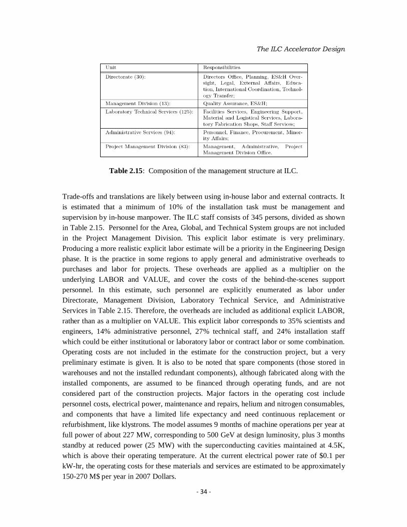
- 34 -
The ILC Accelerator Design
Table 215 Composition of the management structure at ILC Trade-offs and translations are likely between using in-house labor and external contracts It is estimated that a minimum of 10 of the installation task must be management and supervision by in-house manpower The ILC staff consists of 345 persons divided as shown in Table 215 Personnel for the Area Global and Technical System groups are not included in the Project Management Division This explicit labor estimate is very preliminary Producing a more realistic explicit labor estimate will be a priority in the Engineering Design phase It is the practice in some regions to apply general and administrative overheads to purchases and labor for projects These overheads are applied as a multiplier on the underlying LABOR and VALUE and cover the costs of the behind-the-scenes support personnel In this estimate such personnel are explicitly enumerated as labor under Directorate Management Division Laboratory Technical Service and Administrative Services in Table 215 Therefore the overheads are included as additional explicit LABOR rather than as a multiplier on VALUE This explicit labor corresponds to 35 scientists and engineers 14 administrative personnel 27 technical staff and 24 installation staff which could be either institutional or laboratory labor or contract labor or some combination Operating costs are not included in the estimate for the construction project but a very preliminary estimate is given It is also to be noted that spare components (those stored in warehouses and not the installed redundant components) although fabricated along with the installed components are assumed to be financed through operating funds and are not considered part of the construction projects Major factors in the operating cost include personnel costs electrical power maintenance and repairs helium and nitrogen consumables and components that have a limited life expectancy and need continuous replacement or refurbishment like klystrons The model assumes 9 months of machine operations per year at full power of about 227 MW corresponding to 500 GeV at design luminosity plus 3 months standby at reduced power (25 MW) with the superconducting cavities maintained at 45K which is above their operating temperature At the current electrical power rate of $01 per kW-hr the operating costs for these materials and services are estimated to be approximately 150-270 M$ per year in 2007 Dollars
- 35 -
Chapter 3
Klystron Modulator Power Supplies
31 Modulator charging PS design requirements The baseline design for the International Linear Collider outlined in the Reference Design Report [8] envisions two parallel tunnels for each main linac an accelerator tunnel housing the beamline itself and a service tunnel containing the RF sources ndash power supplies modulators and klystrons ndash that power it through waveguide penetrations A primary goal of the current ILC design phase is to identify and evaluate cost-saving options The Modulators are used to generate the pulsed power for the klystrons of 13 GHz Radio Frequency superconducting cavities of the International Linear Collider They have been able to produce rectangular high voltage pulses of with amplitude of 120 kV corresponding a nominal current of 120 A 2 ms of pulse width and a repetition rate of 10 Hz Besides the droop of high voltage pulses must be around 1 of nominal value The electrical power during the pulse is typically 15 MW and can be at maximum 168 MW This leads to a needed pulsed power of 89 GW It is obvious that this energy can not be taken from the mains directly Therefore it is stored in capacitor banks to be released during the pulse DCDC switching power supply is needed to recharge the main capacitor banks and to decouple the low repetition rate from the mains General requirements of a DCDC switching power supply to the charge the klystron modulators are mentioned as follows
bull Maximum charge voltage= 12 kV
bull Pulse repetition rate = 10 Hz
bull Average power per modulator = 300 kW
bull Power factor ~94
bull Total line voltage variation at 5divide10 Hz = plusmn05
bull Maximum efficiency
bull The Main Capacitor Bank (MCB) loaded with constant power minimum ripple phase distortions and an accuracy of plusmn05
bull Maximum power factor of the rectifier feeding the charge device by both decreasing the harmonic composition of the consumed current and by the high value of cosφ
bull The low repetition rate (5divide10 Hz) has to be suppressed in order not to produce disturbances to the mains
- 36 -
Klystron Modulator Power Supplies
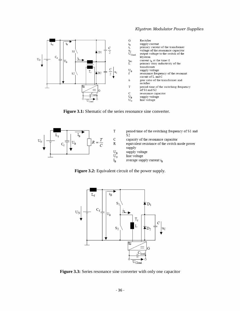
Figure 31 Shematic of the series resonance sine converter
Figure 32 Equivalent circuit of the power supply
Figure 33 Series resonance sine converter with only one capacitor
- 37 -
Klystron Modulator Power Supplies
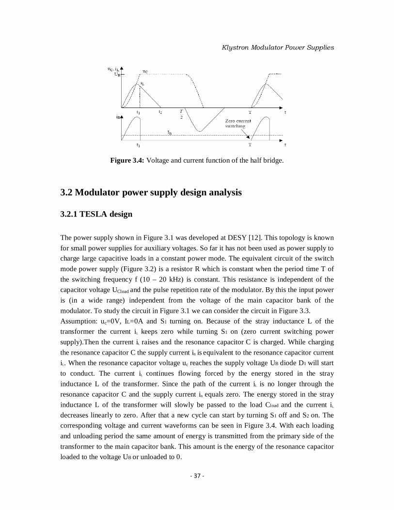
Figure 34 Voltage and current function of the half bridge
32 Modulator power supply design analysis 321 TESLA design
The power supply shown in Figure 31 was developed at DESY [12] This topology is known
for small power supplies for auxiliary voltages So far it has not been used as power supply to
charge large capacitive loads in a constant power mode The equivalent circuit of the switch
mode power supply (Figure 32) is a resistor R which is constant when the period time T of
the switching frequency f (10 ndash 20 kHz) is constant This resistance is independent of the
capacitor voltage UCload and the pulse repetition rate of the modulator By this the input power
is (in a wide range) independent from the voltage of the main capacitor bank of the
modulator To study the circuit in Figure 31 we can consider the circuit in Figure 33
Assumption uc=0V IL=0A and S1 turning on Because of the stray inductance L of the
transformer the current iL keeps zero while turning S1 on (zero current switching power
supply)Then the current iL raises and the resonance capacitor C is charged While charging
the resonance capacitor C the supply current iB is equivalent to the resonance capacitor current
iL When the resonance capacitor voltage uc reaches the supply voltage UB diode D1 will start
to conduct The current iL continues flowing forced by the energy stored in the stray
inductance L of the transformer Since the path of the current iL is no longer through the
resonance capacitor C and the supply current iB equals zero The energy stored in the stray
inductance L of the transformer will slowly be passed to the load Cload and the current iL
decreases linearly to zero After that a new cycle can start by turning S1 off and S2 on The
corresponding voltage and current waveforms can be seen in Figure 34 With each loading
and unloading period the same amount of energy is transmitted from the primary side of the
transformer to the main capacitor bank This amount is the energy of the resonance capacitor
loaded to the voltage UB or unloaded to 0
- 38 -
Klystron Modulator Power Supplies
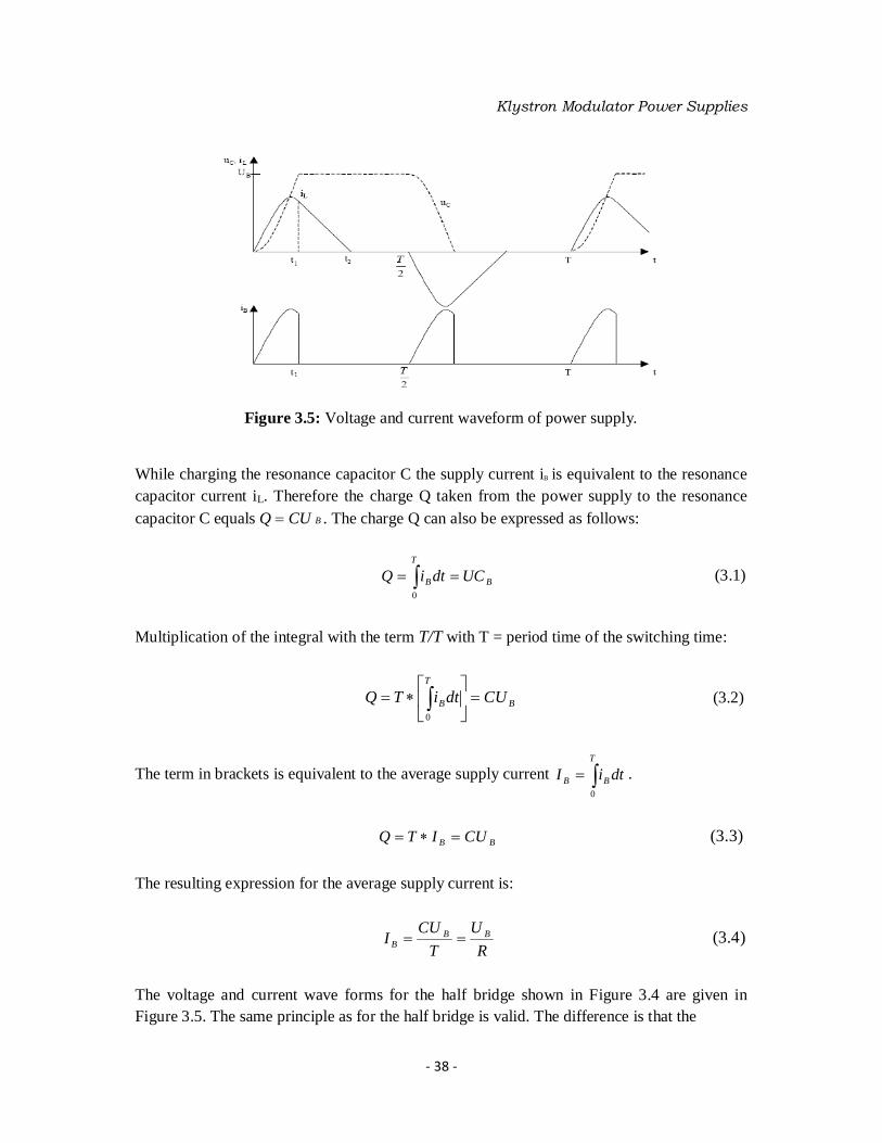
Figure 35 Voltage and current waveform of power supply While charging the resonance capacitor C the supply current iB is equivalent to the resonance capacitor current iL Therefore the charge Q taken from the power supply to the resonance capacitor C equals Q = CU B The charge Q can also be expressed as follows
B
T
B UCdtiQ == int0
(31)
Multiplication of the integral with the term TT with T = period time of the switching time
B
T
B CUdtiTQ =
lowast= int
0
(32)
The term in brackets is equivalent to the average supply current int=T
BB dtiI0
BB CUITQ =lowast= (33)
The resulting expression for the average supply current is
R
U
T
CUI BB
B == (34)
The voltage and current wave forms for the half bridge shown in Figure 34 are given in Figure 35 The same principle as for the half bridge is valid The difference is that the
- 39 -
Klystron Modulator Power Supplies
Figure 36 Simplified circuit diagram of a charge device with an electron protection frequency of the current it doubled and the currents are decreased When one of the capacitors is loaded the second capacitor is unloading and vice versa The required power is with todayrsquos technique hard to fulfill with just one power part A 300 kW prototype consisting of four modules having 75 kW each is going to be tested in TTF One 75 kW module was tested successfully
322 A Russian design for TESLA The basic part of the module is a thyristor inverter converting the input voltage into current pulses at a high repetition rate charging in portions the capacitor up to the required voltage through the step-up transformer (Figure 36) The inverter consists of two loops The first loop consist of a main rectifier G thyristors T1 and T2 a choke L1 and dosing capacitors C0 the second loop includes capacitors C0 thyristors T3 and T4 diodes D1divideD4 and a storage capacitor Cn The step-up transformer Tp used only to transform the inverter output voltage The inverter works in the following way Capacitors C0 are charged in succession from a low-voltage mains rectifier G up to its two-fold voltage by switching on thyristors T1 and T2 through the inductance L1 Every half-period of the inverter operation they transfer their energy to the capacitor Cn being discharged by switching T3 and T4 through the inductance L2 to the primary winding of the transformer Tp For a complete energy transfer from C0 to Cn they are shunted by diodes D1 and D2 With the help of these diodes there is no over-charging of the capacitors C0 the energy is completely transferred to capacitor Cn and there are provided initial conditions for the next charge cycle The last process is the most principle one in the inverter operation W e have situation when the rectifier inside the charge interval works to dosing capacitors with zero initial conditions Uc0 = 0 But the capacitors C0 are discharged completely with a full energy transfer to the storage capacitor Cn only to the value Ucn = UG n (UG = 500 V is the voltage at the rectifier n is the transformation ratio of the transformer Tp)
- 40 -
Klystron Modulator Power Supplies
With a further increase in the voltage on Cn the capacitors C0 donrsquot discharge completely which leads to a reduction in the average value of the consumed current and a violation of the constant power consumption from the mains The capacitor charging is finished at Ucn ~ (105divide11)UGn which is the maximum tolerable over-voltage in the circuit Thus the range 0 lt Ucn lt UGn is the condition for the optimal operation at a constant power consumption The control of the charge voltage level is performed by varying the pulse repetition rate of the inverter The maximum pulse repetition rate corresponds to the continuous inverter operation and the maximum charge voltage The voltage decreases with the pulse repetition rate The thyristors are triggered by means of a functional ldquovoltage-frequencyrdquo converter which is controlled with the help of a variable reference voltage The operation of a single charging device provided the mean power consumed from the mains is constant is characterized by ripples with drops to zero in the intervals between the charge pulses At a maximum repetition rate the phase shift between the sinusoidal charge pulse of the current is equal to π In this case the efficiency coefficient Kef = Iav Imax (Imax-maximum value of current) is equal to 0637 and decrease with the increase in the phase shift during the voltage drop in the process of control The multi phase design of the charge system decreases fluctuations and makes the efficiency coefficient equal to Kef = 09 in the two-phase variant for the phase shift by π2 095 and 097 in the three - and four - phase variants respectively The inverter doesnrsquot require an insulating mains transformer in the rectifier G Either one or a number (10divide20) of inverters can operate from one high-current rectifier Between the rectifier and the inverter an electron switch is used It works together with emergency switches which are of a comparatively slow action The protection circuit operates as follows the capacitor C charged from the low power rectifier (50divide100 W)( in the indicated polarity is in a waiting mode During the alarm situation for example when the operation fails or inverter sticks the rectifier current feeding the inverter goes out of the design mode In this moment when it reaches the determinate level the thyristor T is switched on by a comparator signal and the reverse voltage from the capacitor C is applied o the inverter thyristors T1 and T2 at the same time the trigger pulses are taken off The thyristor which was switched on at that moment (T1 or T2) switches off the inverter alarm current is taken over by the circuit the capacitor C the thyristor T and one of diodes D After the polarity reversal of the C the thyristor T is switched off and the protection circuit is restored It seems advantageous to employ the following scheme of a power supply for the TESLA modulators
bull Each inverter is located near the modulator It is connected to the rectifier through contactor
bull The contactor is remote-controlled in emergency situations it is automatically disconnected
Many of charge devices are based on thyristor rectifiers where the capacitor charge mode is preset by a thyristor switch phase As a rule the thyristor switch phase is close to π at the beginning of the charge interval and as the capacitor is being charged it decrease approaching at the best value of the mains phase ie π3 This fact impairs the harmonic composition of the consumed current and leads to a charge of cosφ inside the charge interval
- 41 -
Klystron Modulator Power Supplies
Figure 37 Fermilab DC power supply 106 kV 14 A The charge systems with thyristor regulators reduce the rectifier power factor It is known
that the rectifier power factor χ depends on the shift factor cos(φ) as well as on the distortion
factor ν
ϕνχ coslowast= (35)
So some disadvantages of the charge system described are
bull The charge device is based on the inverter that is as a powerful frequency converter
a source of radio interference voltage That is why it is necessary to connect an
interference filter at its input The industry produces a great number of interference
filters for different currents and voltages with a working damping of 60 80 and 100
dB
bull The inverter is a source of noises of the sound range the main sources of noises are
the chokes L1 L2 and the transformer Tp We partially decrease this disadvantage
placing these elements in a tank filled with transformer oil
- 42 -
Klystron Modulator Power Supplies
0
2000
4000
6000
8000
10000
12000
14000
000 005 010 015 020 025 030
Time [sec]
Voltage [volts]
0
5
10
15
20
25
30
35
Current [amps]
Choke Current(PS Output)
Choke outputVoltage
(Capacitor C1)
Idealized Choke InputVoltage (PS Output)see below for detail
6000
8000
10000
12000
14000
0000 0004 0008 0012 0016Time [sec]
Voltage [Volts]
Figure 38 PS Voltage Current and Capacitor Voltage 323 Fermilab power supply The Figure 37 represents the Fermilab modulator DC power supply now under test in a ILC test facility called Meson Area The principal parts of the DC power supply are
bull A rectifier transformer composed by a step-up transformer to increase the voltage primary (420 Vac) with a three-phase rectifier non controlled bridge to straighten the current waveform
bull A big choke to level the charging current at 5 Hz with these specifications - 3 Henries plusmn 7 at 60 Hz - Less than 3 kW total losses under the operating conditions - A current of 285 Amps RMS maximum 32 Amps peak - No less than 90 of nominal inductance at 36 Amps
bull A primary phase controller to regulate the operating voltage The advantages of this power supply are
bull Simplicity
bull Relative low cost
- 43 -
Klystron Modulator Power Supplies
Figure 39 Series connection of a diode and a SCR bridge
Figure 310 Voltage curve form of the main capacitor bank in the modulator In other hand the disadvantages of the device are
bull The necessity to have an holding current network for the SCRs use bull The burden and the price of the large 3H choke
bull The high variation of the power supply output current waveform as shown in Figure 38
324 SCR series with a diode rectifier When we looks at the waveform of the capacitor bank the modulator voltage (Figure 310) can be divided into two parts There is a constant DC part and a part of varying voltage The basic idea is to produce the constant DC part with an unregulated diode rectifier The changing part will be produced by a switched mode power supply eg a buck converter By this combination the full regulation dynamic of the switched mode supply can be used Since the price of the diode rectifier is app 40 to 50 of the price of a switched mode supply an overall price reduction of 20 to 30 seems possible depending on the chosen value of the DC voltage
- 44 -
Klystron Modulator Power Supplies
Figure 311 Voltage curve of series connection of diode and SCR Bridge
The same basic idea as for the hybrid supply is assumed Here the switched mode supply shall be replaced by SCR technology to further reduce cost The voltage of the diode rectifier is at 10 kV The SCR has to be in inverter mode at the beginning of the loading period to decrease the voltage At the end of the loading period the power supply has to add voltage A principle schematic is shown in Figure 39 The voltage curves are shown in Figure 311 3241 SCR bridge with a single phase control The power of the SCR supply can be calculated P real power αcos Ldi IUP =
Q reactive power 20
21 QQQ +=
S apparent power 22 QPS +=
Q1 fundamental reactive power αsin1 Ldi IUQ =
Q0 harmonics reactive power Ldi IUQ 3100 =
S1 fundamental apparent power Ldi IUS 1 =
α trigger angle
- 45 -
Klystron Modulator Power Supplies
Figure 312 Real and reactive power in dependence of the phase angle α The correspondence of the reactive power to the real power in dependence of the trigger angle is shown in Figure 312 The overall real power is LdLditdiodethyristor IUIUPPP cos +=+= α
For a constant power α can be calculated
minus=
ditdid
L UU
I
PArc
1cosα
The arccos function is only valid when dit
didL U
UI
P 1minus is between -1 and 1
If the relation
ditdid
Lditdid UU
PI
UU
P
minuslele
+ (36)
is not valid no phase shift angles can be calculated for a constant power mode The simulation shows that a constant power mode is possible when having a nominal voltage of 3 kV of the SCR supply The power diagram is shown in Figure 313 The power was calculated in periods of 20 ms the repetition rate is 10 Hz 3242 Digital regulation The regulation is a major part of a constant power supply The voltage of the capacitor bank at the trigger time of the pulses has to have a pulse to pulse repetition accuracy of +- 05 This in combination with the demand of constant power requires a digital regulation To be able to react on variations of the mains temperature effects or non linear behavior of components the regulation is self learning A simplified modulator circuit is shown in Figure 314 The regulator contains a RAM wherein the charging curve of the capacitor voltage UCload is stored It is driven according to the RAM curve A fast regulator ensures that the
- 46 -
Klystron Modulator Power Supplies
Figure 313 Power diagram of a series connection of a diode and SCR bride α(P)
Figure 314 Simplified modulator circuit
- 47 -
Klystron Modulator Power Supplies
Figure 315 Voltage curve of the main capacitor
Figure 316 Stored reference charging curve of the capacitor
Figure 317 Input power of the modulator
RAM curve and the capacitor voltage UCload are equal despite of even fast voltage variations of the mains voltage UMAINS For this reason it is obvious that the final voltage Ue= UCload at time te remains the same at each charging cycle because it equals the well known RAM curve Figure 315 shows again the voltage curve of the main capacitor bank For achieving constant input power a learning process is introduced A voltage charging curve for Cload is determined With this curve the final charging voltage equals the nominal voltage (Vcapend=Vcapendref) This charging curve is stored in the memory The possible starting curve is shown in Figure 316 With this reference charging curve the input power is not yet constant but looks eg like the curve shown in Figure 317 The aim is to have a constant power With the self learning algorithm the stored reference curve is modified in such a way that the reference values are increased or decreased until the input power is constant The result of the learning process is equal output voltage UCload= Ue = constant after each charging cycle T and constant input power consumption Pin = Paverage = constant
- 48 -
Klystron Modulator Power Supplies
Figure 318 RAM curves of the capacitor reference curves
Figure 319 Linearized and scaled reference curve and monitored curve
Figure 320 Output signal of the regulation To be independent from changes in the charging time T (changes in repetition rate) or the output voltage Ue a unit curve is stored in the RAM By this it is not necessary to relearn this curve in case of change The unit charging curve is simply scaled to the real time and voltage axis To linearize the regulation the capacitor voltages are used as squared values This is because the energy stored in the capacitor CLoad is proportional to the squared capacitor voltage UCload
2 The linearized curve is stored as RAM curve
cloadloadcload UCW 22
1= (37)
UCloadref
2(t) (reference curve) is the linearized reference value of the squared capacitor voltage UCload
2(t) (actual curve)
- 49 -
Klystron Modulator Power Supplies
Figure 321 Block diagram of the digital self-learning regulation The reference value UCloadrefsup2 and the linearized squared capacitor voltage UCloadsup2 are passed to a P(I) regulator The signal Pref is the signal steering the power consumption of the power supply (Figure 320) It is necessary that the actual input power Pin is proportional to the steering signal Pref (Pin sim Pref) In some power supplies a pre- filter has to be used to ensure that Pin sim Pref Droops of the mains voltage UMAINS are the most disturbing error signals for the P(I) regulator The pre filter in the proposed power supply for TESLA guarantees the independence of the input power Pin from the mains voltage UMAINS (Pref sim Pin ne f(UMAINS)) The hardware of the regulation is based on a programmable ALTERA device The device contains the complete regulation software the pulse firing generation of the switched mode power supply and the interlocks for the power supply The designed board is able to work in local mode A VME interface allows communicating with a control computer to feed in pre-calculated curve forms for the modulator By this the learning time is decreased The regulation scheme is shown in Figure 321
- 50 -
Klystron Modulator Power Supplies
Figure 322 Power supplies with stacked buck converters
325 Series connection of buck converters (stacked unit)
To achieve the high voltage level of the main capacitor bank it is possible to stack a group of
low voltage power supplies This topology is used for power supplies that manufactured in
industry The units are now under construction and will be used for some of the TTF
modulators The power supplies are buck converters each having a nominal voltage of app
750V each 16 modules are stacked to deliver the required voltage of 12 kV The transformer
has a 400 V input and 16 outputs of which 8 outputs are in delta the other 8 outputs are in
star to get less mains harmonics Figure 322 shows the principle diagram of such a power
supply The buck converters are working with a Pulse Width Modulation (PWM) The
overlaid regulation for the voltage and the constant input power is accomplished on an
external board that is developed and provided by DESY The internal regulation of the power
supply is a power regulation The units will receive the power reference signal from the
DESY regulation and transforms this into voltage and current values
- 51 -
Klystron Modulator Power Supplies
Figure 323 The overall layout of buck converter
33 The Buck converter solution The previous chapter has shown several modulator power supply design analysis At this point the basic idea is to realize a modulator power supply project constituted by a high voltage buck converter (or step down) single unit The device that is supplied by an input stabilized high voltage of 14 kV must charge the main capacitor bank (with a project value of 14 mF) of each single modulator with a maximum voltage of about 12 kV as request by ILC reference design report Initially will be shown and explained the schematic of device and in particular will be exposed the requirements of buck converter After a circuit simulation will be implemented to analyze the appropriateness of device functionality with the requirements
331 Buck converter schematic and design requirements The requirements of buck converter are mentioned as follows
bull Constant power functionality bull An input voltage of 14 kV and output voltage of ~12 kV bull The high voltage storage capacitor of the main capacitor bank charged in 100 ms
from 10 kV to ~12 kV considering 10 kV as initial voltage value of main capacitor bank
bull The main capacitor bank discharged in 15 ms from ~12 kV to 10 kV bull A switching frequency of 25 kHz ( and a switching period of 40 micros) bull A duty factor D of 075 divide 086
- 52 -
Klystron Modulator Power Supplies
The Figure 323 shows the circuital structure of the device that will be analyzed The principal parts of buck converter and them functionalities are
An input LC filter that isolates power lines from harmonics generated during the main switch turn-onoff the value of input inductance Lin is 10 microH while the value of input capacitor C1 is 1 mF
A main switch characterized by an IGBT stacked switch working in hard switching It produces a variable voltage proportional to duty factor
A free-wheeling diode D1 that allows path of inductor current during the mains switch turn-off
The main switch and diode RC snubber circuits that limit overvoltage on switches during them turn-off the value of snubber resistance and capacitor chosen are 200 Ω and 1 ηF
A charging inductance Lf that reduces the main capacitor bank charging current ripple to an appropriate value The Lf value can be calculated in the following way The main capacitor bank Cload must be charge in 100 ms from 10 kV to 12 kV Its charging current is
Ams
kVmF
t
VCIc c
load 30100
241 asymplowast=
∆
∆lowast= (38)
Now considering the inductance charging current variation of 10 we can calculate the Lfilter value as
mHA
kVkHz
A
kVf
I
VtL
L
L 5133
250
1
3
22
1
conglowast
conglowast
cong∆
lowast∆= (39)
The Rload represents the modulator resistance and in particular the value chosen is 76 Ω
332 Circuit simulations and analysis The circuit simulation have been implemented using WinSpice3 (version 112004) a general-purpose circuit simulation for non-linear DC non-linear transient and linear AC analyses It is based on Spice3 developed by Department of Electrical Engineering and Computer Sciences University of California Berkeley We have performed a transient analysis to computes the transient output variables as a function of time over a user-specified time interval
- 53 -
Klystron Modulator Power Supplies
Figure 324 a) RC Circuit for carrier waveform b) RC Circuit for modulating waveform The initial conditions are automatically determined by a DC analysis that determines the DC operating point of the circuit with inductors shorted and capacitors opened The circuit to be analyzed is described to WinSpice3 by a set of element lines which define the circuit topology and elements values and a set of control lines which define the model parameters and the run controls The main circuit elements and simulation parameters used are
bull Linear resistors capacitors and inductors
bull Diode and voltage controlled switches
bull DC voltage sources and independent sources as pulse sources to switches control bull A transient period of 1 micros divide 220 ms
Also the use of an ideal element that is highly non-linear such as a switch can cause large discontinuities to occur in the circuit node voltage A rapid change such as that associated with a switch changing state can cause numerical round-off or tolerance problems leading to erroneous results or time-step difficulties So to improve this situation was used
bull A tolerance on transient errors of 10-1 bull A relative tolerance of 10-4
333 Main switch control for constant power The core of project is to generate the control waveform of the main switch to obtain the buck converter constant power functionality The basic idea is to generate a square root waveform with a variable duty factor D variation in the range 075divide 086 to guarantee the charging voltage of capacitor from 10 kV to about 12 kV The square root can be obtained comparing two waveforms a carrier waveform and a modulating waveform
- 54 -
Klystron Modulator Power Supplies
Figure 325 The main capacitor bank as black box
As shown in Figure 324 a) a first RC circuit produces a sawtooth waveform or the carrier waveform that increases linearly each 40 micros (switching period of stacked switch) from 0 V to 10 V and discharge immediately in about 20 ηs Now is important to understand what the modulating waveform to obtain constant power is Seeing the storage capacitor as a black box we can write the following system of equations
=
lowast=
dt
dVCtI
tItVtP
claodc
cc
)(
)()()( (310)
To obtain constant power means
dt
dVC
tV
k
tV
ktIktP c
loadcc
c =rArr=rArr=)()(
)()( (311)
and integrating the two members we obtain
intint =t
tload
V
V
c dtC
KdVV
00
(312)
where V0 is the initial voltage of capacitor and V its final voltage while t0 is the initial time and t is the final time of charge Resolving the integral we have the expression of voltage waveform to charge the capacitor for constant power functionality as
21
02
0
2)(
2)(
minus+= t
C
KVt
C
ktV
loadloadc (313)
- 55 -
Klystron Modulator Power Supplies
Figure 326 Control waveform of main switch for constant power
Considering loadC
k2=α and 0
20
2)( t
C
kV
load
minus=β the equation becomes
[ ] 21
)( βα +lowast= ttVc (314)
The relation (314) represents the analytical solution at our problem In our case α = 1771 and β = 5625 and so
25561177)( +lowast= ttVc (315)
is the modulating signal to have constant power At this point a second RC circuit (see Figure 324 b)) produces another saw tooth waveform that increases linearly each 100 ms from 0 V to 11 V and it discharges in 15 ms And so with the sqrt command WinSpice3 we have implemented the square root waveform of voltage capacitor described in the relation (315)
- 56 -
Klystron Modulator Power Supplies
Figure 327 Buck converter input current
Figure 328 Main switch output voltage
- 57 -
Klystron Modulator Power Supplies
Figure 329 Main capacitor bank voltage
Figure 330 Modulator output pulses
- 58 -
Klystron Modulator Power Supplies
Figure 331 SILC Converter schematic
334 Buck converter waveforms In this paragraph we will analyzed the results of simulation and in particular will be analyzed
the following waveforms input current main switch output voltage main capacitor bank
voltage and the modulator output voltage The Figure 327 shows the modulator power
supply current it has a maximum value of 18 A After an initial transitory the current
becomes constant in each period of 100 ms And so as the input voltage and the input current
are constants in 100 ms the buck converter works in constant power While as shown in
Figure 328 the main switch output voltage is pretty good and this is proof that the switch
works well In particular itrsquos a square root waveform with a duty factor in the range 075 divide
086 with zero initial voltage and a final value of 14 kV The Figure 329 represents the
modulator main cap bank voltage The voltage increases in 100 ms from ~ 10 kV to 116 kV
and it discharges in 15 ms Moreover the waveform follows the reference or modulating
signal to obtain constant power In the end the Figure 330 illustrates the modulator output
voltage characterized by pulses with a period of time of 15 ms a maximum voltage value of
about 12 kV and a pulse repetition rate of 10 Hz
- 59 -
Klystron Modulator Power Supplies
34 The Switch In Line Converter Innovation in the field of switched power supplies and DCDC converters has recently acquired a new impulse by the phase-shift (PS) control Inherent advantages of this technique in term of constant operating frequency soft switching and dynamic simplicity emerge from proposal of new topologies suited for applications in different ranges of power This chapter will explain an high power DCDC phase-shifted converter the ldquoSwitch In Line Converterrdquo (SILC) [13 14 15 16] characterized by disposition in line of IGBTs and good soft switching performance
Figure 332 SILC switching commands and current waveforms
341 Operation Principle of the SILC Converter
In the Figure 331 the proposed circuit topology of the SILC Converter is shown It consists in the series connection of two switched half bridges (lower HB and upper HB) The inductor current IL is controlled by the phase-lead shift of the commands to S3 S4 relative to the commands to S1 S2 In the Figure 332 the ideal switching sequence and the current waveforms in the windings T1rsquo and into T1 are represented Reference is made to the typical bias condition Vin= 4VO which means that there is the same steady-state voltage on each HB The initial status at t= t0
- of the switches is S1 OFF S2 ON S3 OFF and S4 ON
- 60 -
Klystron Modulator Power Supplies
Figure 333 Dependence f the output current on the phase shift delay
Figure 334 Phase-shift control characteristic
At t= t0+ S4 turns OFF the current IL flows through Cp4 and Cp3 during the soft switching
interval until D3 clamps S3 turn ON at t= t1- Then since the voltage across L is -2VO IL
decreases and reverses its polarity until it reaches the value ndashILmax at t= t2- when S2 turns
OFF and the output rectifiers too Current balance in the transformer implies that IT1 + I= I T1 - ILmax= 0 hence IT1= I Lmax Another resonant voltage clamped transition identical to the previous one occurs at node 1 Switch S1 turns ON at t= t3
- after clamping of D1 From t3 to t4 the current IL remains constant in this interval the Kirchhoff law implies that IT1 + IL= I 0 where I0 is the output current reflected to the primary side of the transformer When S3 switches OFF (t= t4
-) the second half period begins and it exactly mirrors the first one The period ends at t= t8= t0 + T Power transfer to the load occurs during the time slots t3 ndash t4 and t7 ndash t8 only and it is P= Vin QT where Q is the charge in the shaded area of Figure 60To simplify letrsquos make reference to a single equivalent output voltage VOUT= VO corresponding to a unity winding ratio supplying an output current IOUT= IO so that P= VO IO Being and
(316)
- 61 -
Klystron Modulator Power Supplies
assuming zero ripple in the capacitor that is the output current referred to VO is given
by
(317)
The parabolic dependence of IO on is shown in the Figure 333 where the operative
control range emerges to be 0 ltlt T4 The advantages of the SILC topology are
bull the input voltage partition due the series connection of the half bridges reduces the
stress of the power switches and the voltage transient amplitude at the switching
resonance
bull the converter acts like a controlled current generator
bull increased ZVS range and efficiency
bull ldquointegrated-magneticrdquo feasibility as L can be obtained by the leakage inductance of
T1rsquo
bull non isolated feedback
bull suitability for multiple output in series or in parallel
bull nearly symmetrical soft switching
bull inherent power limitation and short circuit protection
bull natural output voltage clamping
bull high failure tolerance because of the in-line disposition of the switches
bull single pole dynamics
342 The 30 kW SILC Project
The previous chapter has shown the detailed SILC operation At this point the basic idea is to
realize a high DCDC switching power supply constituted by a Switch In Line Converter of
30 kW The device thatrsquos supplied by an input stabilized low voltage of 560 V must charge a
main capacitor bank with a maximum voltage of 14 kV Initially will be exposed the
requirements of SILC After a circuit simulation will be implemented to analyze the
appropriateness of device functionality with the requirements
- 62 -
Klystron Modulator Power Supplies 3421 SILC Design Requirements and Project
The requirements of SILC converter are mentioned as follows bull Constant power functionality bull An input voltage of 560 V and an output voltage of 14 kV bull The main capacitor bank charged in 100 ms up till 14 kV
bull The main capacitor bank discharged in 2 ms from 14 kV to 13 kV considering a droop voltage of 100 V
bull A load current of 1200 A
bull A switching frequency of 15 kHz ( and a switching period of 66 micros) bull A duty cycle D of ~ 50
According with these requirements the values of components was chosen as follows
bull the final level voltage of main capacitor bank is 14 kV Also the main capacitor bank supplies load with 1200 A in 2 ms Assuming a droop voltage of the main capacitor bank equals to 100 V the value of the capacitor is
(318)
bull the value of load resistance is
(319)
bull assuming that at the end of transient time the input capacitors are charged to a level
voltage of 140 V the transformer has a turns ratio of 110 Besides being the charging current of the main capacitor bank is about ~25 A the primary current of the transformer is about ~250 A At this point the magnetizing inductance of transformer can be determined by the following equation
(320)
considering and
bull the value of input capacitors is 50 mF and of inductor L is 5 microH
- 63 -
Klystron Modulator Power Supplies
Time
100ms 101ms 102ms 103ms 104ms 105ms 106ms 107ms 108ms 109ms 110msV(S11)- V(S12) V(S21)- V(S22)
-20V
0V
20V
SELgtgt
V(S31)- V(S32) V(S41)- V(S42)-20V
0V
20V
Figure 335 Switches control signals in the range time 0 lt t le 100 ms
Time
13000ms 13001ms 13002ms 13003ms 13004ms 13005ms 13006ms 13007ms 13008ms 13009ms 13010ms 13011msV(S11)- V(S12) V(S21)- V(S22)
-20V
0V
20V
SELgtgt
V(S31)- V(S32) V(S41)- V(S42)-20V
0V
20V
Figure 336 Switches control signals after 100 ms
Tφ1 = 11 micros
Tdead = 1 micros
Tφ2 = 9 micros
- 64 -
Klystron Modulator Power Supplies
3422 Circuit Simulations and Analysis
The circuit simulations have been implemented using the Schematic session of OrCad 92 a general-purpose circuit simulation for non-linear DC non-linear transient and linear AC analyses We have performed a transient analysis to computes the transient output variables as a function of time over a user-specified time interval The initial conditions are automatically determined by a DC analysis that determines the DC operating point of the circuit with inductors shorted and capacitors opened The main circuit elements and simulation parameters used are
bull Linear resistors capacitors and inductors
bull Power diode and power switches (IGBT)
bull A step-up transformer with a coupling factor k= 0999
bull DC voltage sources and independent sources as pulse sources to switches control
bull A transient period of 3 s
Also the use of an ideal element that is highly non-linear such as a switch can cause large discontinuities to occur in the circuit node voltage A rapid change such as that associated with a switch changing state can cause numerical round-off or tolerance problems leading to erroneous results or time-step difficulties So to improve this situation was used
bull A tolerance on transient errors of 10-1
bull A relative tolerance of 10-4
3423 Control Signals of Switches According to the relation (317) the control of transfer power with the SILC topology is obtained with the control of the phase-lead shift of the commands to S3 S4 relative to the commands to S1 S2 In particular the maximum transfer power is achieved when Tφ= T4 as well shown in the Figure 334 In the project was assumed a topology of control that consists to lead the switches commutation with a high value of Tφ until 100 ms and after the switches are controlled with a less Tφ so that it is possible to control that the main capacitor bank is charged at level of voltage required Accurately the values of Tφ chosen are
- Tφ1= T6= 11 micros ( 0 lt t le 100 ms) - Tφ2~ T7= 9 micros ( after 100 ms )
The Figures 335 and 336 show the control waveforms for switches
- 65 -
Klystron Modulator Power Supplies
Time
20618600s 20618800s 20619000s 20619200s 20619400s 20619600s 20619800s 20620000s 20620200s20618452sI(L) I(L2)
-400A
-200A
0A
200A
400A
Figure 337 Transformer primary current windings T1rsquo and T1
Time
20788800s 20789000s 20789200s 20789400s 20789600s 20789800s 20790000s 20790200s 20790400s20788664sV(L11)- V(L12) V(L22)- V(L21)
-400V
-200V
0V
200V
400V
Figure 338 Transformer primary voltage windings T1rsquo and T1
- 66 -
Klystron Modulator Power Supplies
Time
20788800s 20789000s 20789200s 20789400s 20789600s 20789800s 20790000s 20790200s 20790400sV(L31)- V(L32) V(L42)- V(L41)
-200KV
0V
200KV
-377KV
336KV
Figure 339 Voltage of the transformers secondary windings T1rsquo and T1 in the configuration
with center-tapped transformer
Time
20861500s 20862000s 20862500s 20863000s 20863500s20861191s 20863997sV(Do12)- V(Do11) V(Do22)- V(Do21)
0V
20KV
40KV
50KV
Figure 340 Voltage on the rectifier diodes in the configuration with center-tapped
transformer
- 67 -
Klystron Modulator Power Supplies
Time
2090240s 2090280s 2090320s 2090360s 2090400s 2090440s 2090480s 2090509sV(L31)- V(L32)
-10KV
0V
10KV
-15KV
15KV
Figure 341 Voltage of the transformers secondary windings relatively at Graetz bridge configuration
Time
20875000s 20875200s 20875400s 20875600s 20875800s 20876000s 20876200sV(Do12)- V(Do11) V(Do22)- V(Do21)
0V
05KV
10KV
14KV
Figure 342 Voltage on the rectifier diodes in the configuration with Graetz bridge
- 68 -
Klystron Modulator Power Supplies
Time
200s 201s 202s 203s 204s 205s 206s 207s 208s 209s 210sV(Cload2)
128KV
132KV
136KV
140KV
144KV
Figure 343 Main capacitor bank voltage
Time
200s 201s 202s 203s 204s 205s 206s 207s 208s 209s 210sI(Cload)
-04KA
0A
04KA
08KA
12KA
Figure 344 Charging and discharging current of the main capacitor bank
- 69 -
Klystron Modulator Power Supplies
3424 SILC Project Waveforms This paragraph analyzes the SILC waveform obtained with circuit simulations Figure 337 shows the current in the transformer primary windings T1rsquo and T1 Itrsquos important to see as the peak value of the current in the primary windings T1rsquo is approximately 250 A Figures 338 and 339 show the voltage of the transformer primary windings T1rsquo and T1 and of secondary windings it can be notice that transformer works well While is fundamental to see the voltage on the rectifier diodes It possible understands as the voltage stress on the diodes is more less in the Graetz bridge than in the configuration with center-tapped transformer In fact as possible well to see in the Figure 342 the maximum voltage value on a rectifier diode is 14 kV while the Figure 340 shows that the rectifier diode is submitted to an hard voltage stress with a voltage value that is perfectly double respect to Graetz bridge configuration Also an important particular is shown in the Figure 339 They represent the waveforms relatively at voltage across the transformer secondary windings in the Graetz bridge configuration of the rectifier And so it is important to see as the voltage stress is not presented differently as shown in the Figure 341 Figure 343 represents the main cap bank voltage The voltage increases in 100 ms from 13 kV to 14 kV and it discharges in 2 ms with a droop voltage of 100 V While as shown in the Figure 344 the main capacitor bank absorbs in 100 ms a constant charging current and so the converter is functioning in constant power besides in 2 ms the capacitor supplies the load with a peak current of 1200 A 3425 Soft Switching Commutation
Power semiconductors are the heart of switching mode power supplies A soft switching commutation in several power converters itrsquos important to reduce the conduction losses and switching losses There are two main soft-switching approaches that are the zero-current switching (ZCS) and the zero-voltage switching (ZVS) The choice depends on the semiconductor device technology that will be used For example Mosfetrsquos present better performance under ZVS This is because under ZCS the capacitive turn-on losses increase the switching losses and the electromagnetic interference (EMI) 34251 Snubbers circuits
To perform a soft switching commutation in the power converters typically are used the snubber circuits [17] Snubbers are circuits which are placed across the semiconductor devices to reduce the electrical stresses placed on a device during switching by a power electronics converter top levels that are within the electrical ratings of the device More explicitly a snubber circuit reduces the switching stresses to safe levels by
bull Limiting voltages applied to devices during turn-off transients
bull Limiting device currents during turn-on transients
- 70 -
Klystron Modulator Power Supplies
Figure 345 Commutation waveforms
Figure 346 Switching loci relatively to hard turn-on and turn-off of a semiconductor
device
- 71 -
Klystron Modulator Power Supplies
Figure 347 Circuit configuration of turn-off snubber
Figure 348 Circuit configuration of turn-on snubber
Figure 349 Switching trajectories with and without turn-on snubber
- 72 -
Klystron Modulator Power Supplies
Figure 350 IGBT circuit symbol and equivalent circuit
bull Limiting the rate of rise (didt) of currents through devices at device turn-on
bull Limiting the rate of rise (dvdt) of voltages across devices during its turn-off or during reapplied forward blocking voltages (eg SCRs during the forward blocking state)
bull Shaping of switching trajectory of the device as it turns on and off to keep the functioning of the devise inside its safe operating area (SOA)
bull Limiting total losses due to switching
bull Limiting EMI by damping voltage and current ringing From circuit topology perspective there are three broad classes of snubber circuits These classes include
bull Unpolarized series R-C snubbers used to protect diodes and thyristors by limiting the maximum voltage and dvdt at reverse recovery
bull Polarized R-C snubbers These snubbers are used to shape the turn-off portion of the switching trajectory of controllable switches to clamp voltage applied to the device to safe levels or to limit dvdt during device turn-off The Figure 347 shows an example of this type of snubbers
bull Polarized L-R snubbers These snubbers are used to shape the turn-on switching trajectory of controllable switches andor to limit didt during device turn-on The Figure 348 shows an example of this type of snubbers and the Figure 349 shows the shape of switching trajectory of the device using the turn-on snubber
It must be emphasized that snubbers are not fundamental part of a power electronic converter circuit The snubber circuit is an addition to a basic converter which is added to reduce stresses on an electrical component usually a power semiconductor device Snubbers may be used singly or in combination depending on the requirements The additional complexity and cost added to converter circuit by the presence of the snubber must be balanced against the benefits of limiting the electrical stresses on critical components
- 73 -
Klystron Modulator Power Supplies
- 74 -
Klystron Modulator Power Supplies
Figure 351 Datasheet of CM600HA-12H Power IGBT
- 75 -
Klystron Modulator Power Supplies
Csnubber [nF] Pigbt1 [W] Pigbt2 [W] Pigbt3 [W] Pigbt4 [W] Ptot [W]
120 1200 1290 210 2785 29785
300 1143 1215 12405 2019 268395
500 1088 1161 8494 16765 250159
800 1021 1101 7021 1447 233691
1000 1000 1075 634 140 22784
2000 923 1015 2519 7258 29157
Table 352 Mean power losses and total power losses values depending of snubber capacity
0 200 400 600 800 1000 1200 1400 1600 1800 20002200
2300
2400
2500
2600
2700
2800
2900
3000
Csnubber [nF]
P [
W]
Pz1+Pz2+Pz3+Pz4
Figure 353 Total power losses depending of snubber capacity 3426 Select of SILCrsquos switches
This paragraph will explain what type of switch was selected for the project In particular
after a short description of the switch will be shown the datasheet of device the selection of
the snubber circuit in particular the calculation of snubber capacitance and in the end will be
illustrated the commutation waveforms of switches to verified if the soft switching
requirement is satisfied
- 76 -
Klystron Modulator Power Supplies
34261 Insulated Gate Bipolar Transistors ( IGBTs)
As previously illustrated we have need of four switches that work with high values of
voltage and current and with a low switching frequency (15 kHz) For this reasons IGBT
switches was chosen The circuit symbol and equivalent circuit for an IGBT is shown in
Figure 350
The IGBTs have some advantages of the MOSFETs (Metal-Oxide-Semiconductor Field-
Effect Transistor) the BJT (Bipolar Junction Transistor) and the GTO (Gate Turn-On
Thyristor) combined Similar to the MOSFET the IGBT has a high impedance gate which
requires only a small amount of energy to switch the device Like the BJT the IGBT has a
small on-state voltage even in devices with large blocking voltage ratings (for example Von is
2-3 V in 1000 V device) While similar to the GTO IGBTs can be designed to block negative
voltages as their idealized switch characteristics Besides insulated gate bipolar transistors
have turn-on and turn-off times on the order of 1 micros and are available in module ratings as
large as 1700 V and 1200 A Voltages ratings of up to 3-4 kV are projected and utilized In
the SILC project was utilized the Spice Model of CM600HA-12H the Mitsubishi IGBT
modules with a collector-emitter voltage of 600V and a collector current of 600 A The
datasheet of device is proposed [18]
34262 Choose of Snubber Capacity and Switching Commutations
The aim of this paragraph is explain the procedure for the selection of the the snubber
capacity to guarantee the soft switching of devices in their turn-offs The particular procedure
that was followed is to fix a value of snubber capacity and after a simulation take the value of
mean power loss of a single device considering the turn-on and turn-off The dates
concerning this aspect are listed in the first four columns of the Table 351 while the last
column represent for a particular value of snubber capacity the total mean power loss of all
devices Besides itrsquos important to observe that the topology of SILC converter produce
always in any different case a major stress on the switches of the low half bridge ( IGBT1 and
IGBT2) In fact the Table 352 shows well as the main part of switching power losses derive
from these switches In the end considering the Figure 353 the value of snubber capacity
that was chosen for the project is Cs = 1000 nF
Figures 354 355 356 357 358 359 360 and 361 show the turn-on and turn-off
commutations of IGBTs and in particular itrsquos important to see as ZVS and ZCS commutation
on all IGBTs are guaranteed
- 77 -
Klystron Modulator Power Supplies
Time
694261ms 694262ms 694263ms 694264ms 694265ms 694266ms 694267ms1 IC(Z1) 2 V(Z1C)- V(Z1E)
0A
200A
400A
600A1
gtgt0V
100V
200V
300V2
Figure 354 IGBT1 turn-off
Time
6942960ms 6942970ms 6942980ms 6942990ms 6943000ms 6943010ms 6943020ms1 IC(Z2) 2 V(Z2C)- V(Z2E)
0A
200A
400A
600A1
gtgt0V
100V
200V
300V2
Figure 355 IGBT2 turn-off
Time
6943170ms 6943180ms 6943190ms 6943200ms 6943210ms 6943220ms 6943230ms1 IC(Z3) 2 V(Z3C)- V(Z3E)
0A
200A
400A
600A1
gtgt0V
100V
200V
300V2
Figure 356 IGBT3 turn-off
Time
69435300ms 69435400ms 69435500ms 69435600ms 69435700ms 69435800ms 69435900ms69435227ms1 IC(Z4) 2 V(Z4C)- V(Z4E)
0A
200A
400A
600A1
gtgt0V
100V
200V
300V2
Figure 357 IGBT4 turn-off
- 78 -
Klystron Modulator Power Supplies
Time
692846ms 692848ms 692850ms 692852ms 692854ms 692856ms 692858ms 692860ms1 IC(Z1) 2 V(Z1C)- V(Z1E)
0A
200A
400A
600A1
gtgt0V
100V
200V
300V2
Figure 358 IGBT1 turn-on
Time
69287800ms 69288000ms 69288200ms 69288400ms 69288600ms 69288800ms 69289000ms 69289200ms69287643ms1 IC(Z2) 2 V(Z2C)- V(Z2E)
0A
200A
400A
600A1
gtgt0V
100V
200V
300V2
Figure 359 IGBT2 turn-on
Time
69290000ms 69290500ms 69291000ms69289771ms 69291409ms1 IC(Z3) 2 V(Z3C)- V(Z3E)
0A
200A
400A
600A1
gtgt0V
100V
200V
300V2
Figure 360 IGBT3 turn-on
Time
6929300ms 6929320ms 6929340ms 6929360ms 6929380ms 6929400ms 6929420ms 6929440ms1 IC(Z4) 2 V(Z4C)- V(Z4E)
0A
200A
400A
600A1
gtgt0V
100V
200V
300V2
Figure 361 IGBT4 turn-on
- 79 -
Chapter 4
A Solid State Marx Modulator for ILC 41 Introduction The Main Linac of the International Linear Collider will require in order to accelerating electrons and positron up to center of mass energy of 500 GeV per collision 576 Radio Frequency (RF) stations Each RF station will power a 10 MW L-band klystron that will provide the acceleration energy to 26 niobium superconducting cavities Each cavity has a design accelerating gradient of 35 MeVm The 10 MW L-band klystron will be supplied by a modulator which have to be capable to produce an output pulsed signal with a width of 2 ms a repetition rate of 10 Hz an amplitude of 120 kV for a current of 120 A These design parameters correspond to output energy of about 27 kJ The output pulse droop have to stay under the nominal value of about 1 In the existing Fermilab Baseline Conceptual Design (BCD) the klystron modulator generally called Bouncer Modulator has a transformer-based topology The Bouncer Modulator was developed at the Fermi National Accelerator Laboratory (FNAL) near to Batavia Illinois (USA) It will be tested starting from summer 2010 in the Fermilab ILC Test Facility at New Muon Lab (Figure 41a 41b and Figure 42) The large size weight and cost of this transformer the large capacitors banks as well as the large and expensive oil cooled inductor have been between the motivations of the present RampD work where we want to find alternative topologies that do not employ the use of all these massive and expensive components In order to fit the ILC modulator design requirements we developed a Solid State Marx Modulator (SM2) that uses solid state switches (IGBTs) and isolation elements to connect capacitors in parallel while charging and in series during the capacitor discharge
42 The Fermilab Bouncer Modulator The Bouncer Modulator is a transformer based large inductor modulator developed by the Fermilab Accelerator Division [26 27 28 29 30] The main layout of this apparatus is shown in Figure 43 This modulator uses a large size switched capacitor bank of 14 mF that droops approximately of 20 during the full pulse width This very large droop is then compensated by using a resonant LC circuit If the capacitor bank is connected to the high side of the pulse transformer primary using a series of GTO switches instead the resonant circuit is connected to the low side of the pulse transformer primary The resulting output pulse is flat within 1 for 19 ms of the full 23 ms pulse width fitting the design request
- 80 -
A Solid-State Marx Modulator for ILC
Figure 41 a) The New Muon Lab building b) the ILC Test Facility at the New Muon Lab
Figure 42 Layout of the beam line and service apparatus cooling RF lines klystron Modulator etc in the New Muon Lab complex
- 81 -
A Solid-State Marx Modulator for ILC
The Fermilab Bouncer Modulator has been tested and it is efficiency measured from breaker
to klystron including energy losses in the rise time These measurements show that the
Bouncer Modulator has an efficiency of 85
421 Operational Principle
The Bouncer Modulator operational principle is the following The main capacitor bank C1
is charged approximately at a value that is 10 higher than what required output voltage
while the bouncer circuit elements L3 (600 microH) and C2 (2 mF) in Figure 43 are charged to
10 of the required output voltage In order to produce a long output pulse width the
bouncer resonant circuits switch S4 is closed and the capacitor starts to ring with the
inductor At the appropriate time the GTO switch S1 connecting the main capacitor bank to
the pulse transformer is closed Then after 2 ms the GTO switch is opened The bouncer
circuit then continues to ring through is full cycle
422 The Bouncer Modulator key components and costs
The Fermilab Bouncer Modulator is done by several components that are custom A reliable
and robust closing and opening switches are required so a series stack of six Gate Turn Off
Thyristors (GTO) are used Recently IGBTs switches are used as a replacement for GTOs
switches because of their higher reliability lower cost and better switch control [27] Figure
44 shows the Bouncer Modulator with a series stack of seven IGBTs The bouncer circuit
must be designed with low loss and the maximum impedance consistent with effective output
regulation The main capacitor bank must be designed for a crowbar operation and capacitor
fault conditions The pulse transformer (with 112 turns ratio) must have a very large volt
second rating and a relatively low leakage inductance (317 microH) Moreover mechanical
vibration from the system must be kept to a minimum because the RF superconducting
cavities are nearby The cost for the Bouncer Modulator components have been of about 370
k$ This prize includes approximately 20 k$ spent for buying the control system 50 k$ for
the GTO switches 75 k$ for the 400V AC phase controller and for the power transformer and
90 k$ for the pulse transformer Fermilab facility testing and the labor costs have not been
included in the present list of the costs
- 82 -
A Solid-State Marx Modulator for ILC
Figure 43 DC power supply and bouncer modulator design with GTOs switches
Figure 44 The Fermilab Bouncer Modulator design with IGBTs switches
- 83 -
A Solid-State Marx Modulator for ILC
43 The Marx Generator Concept 431 Introduction A Marx generator is an electrical circuit introduced for the first time by Erwin Otto Marx in
1924 whose purpose is to generate high-voltage pulses In a Marx generator a set of N
capacitors are charged in parallel to a low input voltage Vin and discharged in series to apply
a high voltage Vout = N Vin to the target load Marx generators are widely used in pulsed
power technologies due to their simplicity scalability and low voltage input requirements
Applications include medical accelerators welding and cutting laser supplies radar systems
and particle accelerators Emerging uses include the sterilization of liquids and foods (via
electroporation) [1920] juice extraction [21] rock crushing [22] electromagnetically-
powered transportation [23] Marx generators are extensively used also for simulating the
effects of lightning during high voltage and for aviation equipment testing Recently a bank
of 36 Marx generators have been used by the Sandia National Laboratories located in
Albuquerque New Mexico (USA) to generate X-rays in their so called Z Machine The Z
machine is the largest X ray source in the world It had been designed to test materials in
conditions of extreme temperatures and pressures This machine can be used also as an
ignition switch for thermonuclear devices At the present Marx generators are also used in
order to produce short high-power pulses for Pockels cells for driving a Transversely Excited
Atmospheric Pressure (TEA) Laser for the ignition of conventional explosive used in the
nuclear weapons and to produce radar pulses The time speed of such a kind of devices is
relatively large as the switching times of even high-speed versions is greater than 1 ns when
many low-power electronic devices are faster In the design of high-speed circuits classical
electrodynamics effects may be important this is not the case of Marx generators where the
basic design is nevertheless essentially an electrostatic one As matter of fact if the first gap
breaks down pure electrostatic theory predicts that the voltage across all stages rises
However stages are coupled capacitively to ground and serially to each other and thus each
stage encounters a voltage rise that is increasingly weaker the further the stage is from the
switching one The adjacent stage to the switching one therefore encounters the largest
voltage rise and thus switches in turn As more stages switch the voltage rise to the
remainder increases which speeds up their operation Thus a voltage rise fed into the first
stage becomes amplified and steepened at the same time The speed of a switch is determined
by the speed of the charge carriers which gets higher with higher voltages and by the current
- 84 -
A Solid-State Marx Modulator for ILC
Figure 45 A classical 4-stages Marx generator circuit
available to charge the inevitable parasitic capacity In solid-state avalanche devices a high
voltage automatically leads to high currents Because the high voltage is applied only for a
short amount of time solid-state switches will not heat up excessively As compensation for
the higher voltages encountered the later stages have to carry lower charge too Stage cooling
and capacitor recharging also go well together
432 The classical layout
A Marx generator in his classical configuration has essentially a resistive-based topology
Figure 45 shows an example of a 4-stages classical Marx generator circuit The operation
principle of this design is characterized by a capacitor C which charges through two
resistances R1 and R2 when the spark gaps S are opened When fully charged the lowest gap
breaks down from overvoltage (or an external trigger) which puts the lowest two capacitors
in series and then over-voltages the second gap and so on Eventually the erected load
voltage is equal to the number of stages N multiplied by the input voltage Vin Likewise the
total erected capacitance at that point is equal to CN The major advantages of this topology
are low voltage input requirements while disadvantages are energy losses through passive
charging elements as well as through chargingdischarging stacked stray capacitances
Further issues may arise from stacking such as deformation of the pulse shape at higher
currents due to increased parasitic inductances Charging resistors may also limit the pulse
fall time as they act as high resistance shunt through which stray capacitances must
discharge
- 85 -
A Solid-State Marx Modulator for ILC
Figure 46 A 3-stages Marx generator layout figure a) shows the current charging path while figure b) gives the discharging current path
- 86 -
A Solid-State Marx Modulator for ILC
Figure 47 An example of 3-stages Solid State Marx Bank employing ideal charge and discharge IGBTs (SC and SD)
433 Solid State Marx Generator In recent years the classical Marx layout has been improved by using semiconductor switches that increase control efficiency and pulse form [24 25] In a Marx design the danger of overvoltage is also minimized because switches donrsquot hold-off large potentials and remain isolated within the subsystems In many cases the improvements consist solely of replacing traditional switches (eg spark gaps) with solid-state devices but traditional passive elements (inductive chokes of resistors) are kept to provide charging paths and stage isolation This is an improvement only half-complete While newer switching technologies bring certain advantages to the fore passive elements continue to inhibit performances through an inherent trade-off between efficiency and duty cycle Charging resistances must be large enough to isolate stages during the discharge (force energy through the load) but small enough to allow rapid recharging in the dead time between pulses This trade-off is the reason for why chokes are now typically used instead of resistors yet they become themselves impractical when longer pulse widths are required To balance the trade-off components are selected for a specific duty cycle A deviation from this configuration is detrimental to performance A solid state Marx generator design is outlined in Figure 46 and in Figure 47 The first shows the general design concept where the passive elements R1 and R2 in Figure 45 have been replaced by a solid state charge and discharge switches SC and SD respectively In order to charge the storage capacitors all switches SD are opened and all
- 87 -
A Solid-State Marx Modulator for ILC
Figure 48 Klystron power supply complex using our Solid State Marx Modulator (SM2)
switches SC are closed Once the capacitors are charged the Marx bank is fired into the load by opening switches SC and closing switches SD At the end of the high voltage pulse their states invert once again to recharge the storage capacitors Figure 43 shows how an ideal Marx bank may be realized through solid-state power components alone In this implementation the charging element R1 of a classical Marx modulator has been replaced by a high voltage switching diode and R2 by an IGBT-based switch The diode has a low impedance path for charging storage capacitors in parallel but provides high impedance isolation during their discharging in series It also provides a bypass path when the SD switch fails to close during the discharge In such a case the system output is simply reduced and the amount of energy remains in the isolated stage This configuration allows the stages to charge simultaneously and therefore enforces an equal share of electrical stresses at all times Note that an active ldquopull-downrdquo through the charge switches SC is inherent in the designs of Figure 46 and Figure 47 Such a feature rapidly discharges stray and load capacitances at the beginning of the charge cycle to give a sharper pulse trailing edge
44 SM2 a Solid State Marx Modulator for ILC SM2 Solid-State Marx Modulator is a transformerless-based solid state Marx generator developed by a group of physicist and engineers of the University of Cassino (Italy) working inside the Istituto Nazionale di Fisica Nucleare (INFN) NTA-ILC Collaboration A solid state Marx topology will not need to use any high voltage transformer As matter of fact this design has several advantages over the conventional klystron modulator designs
it is physically smaller there is no pulse transformer (quite massive for the needed voltages and currents) no need of large energy storage capacitor banks owing to the active droop
- 88 -
A Solid-State Marx Modulator for ILC
Figure 49 The SM2 fundamental cell layout
compensation it is oil-free voltage hold-off is achieved by using air insulation it is air cooled secondary air-water heat exchanger is physically isolated from the electronic
components Figure 48 shows a block diagram of the klystron power supply complex In particular is shown a 300 kW DCDC switching power supply which have to be capable to produce a stabilized input voltage for SM2 The Solid-State Marx Modulator that supplies with particular requirements already mentioned the 10 MW L-band klystron is constituted by a series of two specific circuits The first circuit that will be called also Main Marx (MM) is a solid state switch Marx generator that uses 24 identical fundamental cells The MM is supplied by an input voltage stabilized of 5 kV and it produces an output pulsed signal with a width of 2 ms a repetition rate of 10 Hz an amplitude of 120 kV with a output current of 120 A and a output signal droop of about 13 The second circuit that will be call also Flattener is a solid state switch smaller Marx generator that uses 19 identical fundamental cells to achieve an output drop compensation of about 1 as required by the ILC design report The Flattener is supplied by an input stabilized voltage of 12 kV and it is opportunely fired to reduce the output pulse droop
- 89 -
A Solid-State Marx Modulator for ILC
Figure 410 The Main Marx block layout
441 The SM2 fundamental cell design The layout of the single cell of the SM2 modulator the fundamental cell is shown in Figure
49 The key components of each fundamental cell are
bull a charge diode (Dch) that provides a path for charging the main capacitor (Ccharge) to
input voltage
bull an isolation diode (Diso) that provides isolation between a single cell and the other
cells during erection
bull a charge switch (charge) that provides the charging path for the main capacitor during
a charging period of 100 ms
bull a fire switch (fire) which closure will produce a ndashVin output pulse from the cell of a 2
ms pulse length
bull a by-pass diode (Dbp) that provides a conduction path to the load through the cell or
the cells that have not been fired
bull a series inductor L to limit dIdt in the output current
- 90 -
A Solid-State Marx Modulator for ILC
Figure 411 Marx bank efficiency versus the number of Marx stages for various stray stage capacitances The inset shows a close-up of 10-stages modulator efficiency
442 The SM2 Main Marx Generator In the previous chapter we discussed the layout of a fundamental cell of the SM2 Modulator In this paragraph we will describe the development of a Marx modulator able to produce output pulsed signals of 120 kV for a current of 120 A 2 ms base pulse width and a repetition rate of 10 Hz We will start reviewing the circuit requirements and then we will discuss the results of the simulations performed in order to study the behavior of a fundamental cell and of the full Main Marx generator
4421 The Main Marx Layout and Design Requirements The Main Marx modulator is a Marx generator that uses solid state switches MM uses 24 identical fundamental cells The MM design requirements are the following
bull An input stabilized high voltage of 5 kV and an high output voltage of 120 kV
bull An output voltage droop of about 13
bull An output current of 120 A
- 91 -
A Solid-State Marx Modulator for ILC
Figure 412 Simulated single cell output voltage
Figure 413 Simulated single cell output current
Figure 414 Simulated single cell output energy
- 92 -
A Solid-State Marx Modulator for ILC
bull The main capacitors must charge in parallel in 100 ms at input voltage level
bull The main capacitors must discharge in series to produce an output pulse of 2 ms base pulse width
Because of these requirements we end up to have a MM circuit with a number of cell equal to 24 and a Main Capacitor for storing the circuit energy of 350 microF (Ccharge in Figure 49) The cells have been designed also in an way that each of them accumulate an energy below the value of 118 kJ As matter of fact this energy value is below to the maximum energy that can be reversed to the klystron without risking to damaging it
4422 Stray Capacitance Charging Losses Some of the Marx-stored energy is required to repetitively charge stray capacitances that might be present in the bus work of a modulator This energy cannot be recycled and is lost during the active pull-down The higher modulator resides on the potential ladder the more energy is required to charge inherent stray capacitances CP per stage with respect to ground So the total power lost to this process assuming stray capacitances are well balanced is
sum=
=N
kinpstray kVC
fP
1
2)(2
(121)
Inefficiencies relating to stray capacitance increase quadratically with the number of stages N and as such impose an upper practical limit on the number of stages in a Marx modulator In order to minimize stray capacitances design efforts must reduce the physical size of the modulator footprint components and stage interconnects Curves of efficiencies for various values of stray capacitance are plotted versus number of stages in Figure 411 From this graph it is apparent that at 10 kV the efficiency remains above 90 even with liberal amounts of internal stray capacitances In the SM2 cell layout (Figure 49) the value of stray capacitance was assumed equal to 10 pF 4423 Main Marx output response
The circuit simulations have been implemented by using the schematic session of the OrCad 92 program OrCad is a general-purpose circuit simulation for non-linear DC non-linear transient and linear AC analyses fully owned by Cadence Design Systems We have performed a transient analysis to computes the transient output variables as a function of time over a user-specified time interval The initial conditions were automatically determined by a DC analysis that determines the DC operating point of the circuit with inductors shorted and capacitors opened The main circuit elements and simulation parameters used are
- 93 -
A Solid-State Marx Modulator for ILC
Figure 415 Simulated Main Marx output voltage the droop in the output voltage has a value of about 13
Figure 416 Simulated Main Marx output current the droop in the output current has a value of about 13
Figure 417 Simulated Main Marx output energy
- 94 -
A Solid-State Marx Modulator for ILC
bull Linear resistors capacitors and inductors
bull Stray resistance and capacitance
bull Real power diode and real power IGBTs
bull DC voltage sources and independent sources as pulse sources to switches control bull A transient period of 50 ms
Also the use of an ideal element that is highly non-linear such as a switch can cause large discontinuities to occur in the circuit node voltage A rapid change such as that associated with a switch changing state can cause numerical round-off or tolerance problems leading to erroneous results or time-step difficulties So to improve this situation was used
bull A step ceiling of 10-3
bull A relative tolerance of 10-2
In order to perform a realistic study of the circuit behavior we used in the simulation real circuital elements by implementing real switches and by adding to each circuital component parasitic capacitance and resistance as well as real tolerances These quantities have been also used later in the Montecarlo simulations of the full SM2 Modulator behavior under different operational conditions The output response of our simulations performed on a single fundamental MM cell is given in Figure 412 413 and 414 where the output voltage the output current and the output energy are plotted Figure 415 416 and 417 on the other hand show the behavior of the full Main Marx generator As it is possible to see the droop in the output voltage and in the output current is around 13 of the total voltage and current value (120 kV 120 A)
443 The Flattener circuit In the SM2 Modulator the droop regulation of the output pulses up to a value of plusmn05 is achieved by adding a small Marx in series with the Main Marx This small Marx generator the Flattener circuit is composed of 19 fundamental 12 kV cells similar to the one used for the Main Marx The flattener cells are then fired sequentially in order to be able to generate a series of discrete corrections on the Main Marx output signal droop If we compare this droop compensation strategy to the droop compensation achieved in a bouncer-like correction the conclusions are that our scheme is much smaller and less expensive than the other Figure 418 shows the overall modulator characterized by the Flattener in series with the Main Marx The time regulation of such a system is very crucial in order to achieve the droop compensation up to the design requirements In the next paragraph we will describe how the Flattener charging and discharging switches are fired and in particular we will show the control driving law that must be implemented together with the trigger system in order to obtain a good performance of Flattener circuit
- 95 -
A Solid-State Marx Modulator for ILC
Figure 418 Overall SM2 Marx Modulator layout As it is possible to see in the circuit schematic the Flattener circuit is in series with the Main Marx generator
- 96 -
A Solid-State Marx Modulator for ILC
Figure 419 Full SM2 Modulator conceptual design where STS is the Switching Trigger System for the SM2 modulator MM is the SM2 Main Marx modulator the MMDS is the Main Marx Driving System FDS is the Flattener Driving System and the KEDOSS is the Klystron Energy Droop Out Safety System PS is the SM2 DCDC switching power supply
444 The SM2 Switching Trigger System The implementation of the SM2 Switch Trigger System (STS) is an important part of our solid state Marx generator complex It is mainly based on a general controller that acts on two different digital trigger systems
bull The Main Marx Driving System (MMDS) that is used to generate the control signal sequence for the Main Marx Generator switch charging and discharging The MMDS controls the closing of all charging switches during a period time of 100 ms to allow the main capacitor charging (Ccharge) in parallel and the closing of all the discharging switches during the output signal creation in a period of time of 2 ms
bull the Flattener Driving System (FDS) that is used in order to fire with an appropriate time control sequence the charging and discharging switches of the Flattener circuit in order to open and close sequentially the switches for the Main Marx droop compensation in the high voltage output pulses
It has to be noticed that the MMDS and the FDS must be accurate in order to fire simultaneously all charging switches during the charging time and all discharging switches during discharging period Nowadays the implementation of such an apparatus can be easily achieved by using Field-Programmable Gate Array devices (FPGA) and optical fibers for trigger signal transport Figure 419 gives a schematic overview of the full Solid State Marx
- 97 -
A Solid-State Marx Modulator for ILC
Figure 420 Sequence of the trigger signals necessary to operate the Flattener charging switches
Figure 421 Pulse width of the trigger signals necessary to operate the Flattener discharging switches
- 98 -
A Solid-State Marx Modulator for ILC
Figure 422 Simulated Flattener output voltage
Modulator and Switching Trigger System In Figure 420 421 we report the time sequence needed to trigger the charging and discharging switches of the Flattener In particular Figure 420 shows the sequence of the trigger signals necessary to operate the Flattener charging switches while in Figure 421 the pulse widths of the trigger signals necessary to operate the Flattener discharging switches are illustrated Finally the simulated output signal coming from the Flattener circuit is given in Figure 422
45 Solid State Marx Modulator single Failure Risks The probability of critical component failure increases directly with the number of elements In the basic design scheme the failure of any single IGBT or capacitor will fail the entire modulator by shorting out the input DC power These critical single-point failures must be eliminated in any practical design by using a large numbers of cells with a lower ripple voltage The transmission scheme for vital control data and timing fiducials must also be massively parallel in nature to avoid single-point control-induced failures Failures of any IGBT or capacitor in a basic Solid State Marx Modulator design will fail the entire modulator These single-point risks can be mitigated by adding a simplified high-side IGBT buck regulator to each cell This regulator serves three vital functions
1 Control of inrush currents during the charging cycle 2 Local regulation of the cell operating voltage 3 Isolation of the cell from the main DC charging path in the event of a cell failure
Another important characteristic of any klystron modulator have the protection from arcs when the klystron faults The klystron is a very expensive device and it will probably arc at some time of its life Regarding the ILC TDR klystron model Toshiba MBK 3736 that works typically with the following voltages and currents VIn= 120 kV IIn= 120 A
- 99 -
A Solid-State Marx Modulator for ILC
Figure 423 Simulated voltage (a) and current (b) droop as a function of number of cell that failed in the SM2 modulator
(RLoad= 1 kΩ) the SM2 modulator is expected to deliver an energy to the klystron of about E= RI2T= 288 kJ Then an arc protection system has to be implemented Figure 421 shows the SM2 modulator conceptual design where the Klystron Energy Drop-out Safety System (KEDOSS) is also represented The development of the KEDOSS apparatus goes beyond the goals of the present work Anyhow there are several solutions under consideration The first one that we considered is a conventional crowbar circuit that suddenly quenches the klystron arc into a discharge of the stored energy However the crowbar circuit has false-firing problems caused by electric noise and other crowbarless solutions have been considered In Figure 423a and in Figure 423b we show the simulated current and voltage droop as a function of the number of cell that failed inside the SM2 Modulator The behavior reflects what expected as Marx generator adds to each step linearly the same voltage step-up Vout= NmiddotVcell As the probability of N independent failures inside SM2 goes as PN this plot show that a failure of a single cell doesnrsquot quench the modulator output response
46 The SM2 Marx Modulator circuit simulation and analysis In this paragraph we describe a part of the ample analysis that has been performed in order to study the behavior of our Solid State Marx Modulator design To begin we will show that the ILC TDR design requirements have been achieved Figure 424 shows the simulated SM2 120 kV output train pulses as it possible to see the repetition rate fits the design of a 10 Hz repetition rate modulator Figure 425 shows the simulated SM2 output voltage that goes to power the klystron This distribution has a maximum absolute value of 120 kV a pulse width of 2 ms and the output voltage droop stay below the nominal TDR request of about 1 [31] Figure 426 shows the simulated SM2 output current The plot has a maximum value of 120 A a pulse width of 2 ms and an output current droop that stays below the nominal TDR request of about 1 Besides Figure 427 shows the SM2 produced output energy that supplies the klystron of the needed energy to power the 26 niobium superconducting cavities
- 100 -
A Solid-State Marx Modulator for ILC
Figure 424 Simulated SM2 120 kV output train pulses the repetition rate is 10 Hz As already mentioned before the klystron needs to be powered with an energy per cycle (2 ms) of about 27 kJ As it was mention in the previous paragraphs we implemented a realistic simulation of our Marx generator concept by accounting real parasitic resistances and inductances for every single component in the SM2 modulator and by using real IGBT based switches In order to get a more realistic output response we had the need to perform a Montecarlo simulation Montecarlo simulation is a method of simulation with unknown variables In Montecarlo simulation values for unknowns are randomly selected according to their statistical distribution The process is repeated for a number of pseudo-experiments each with a new set of values for the unknowns The distribution of the final results is taken to be representative of the ldquorealrdquo behavior over the range of inputs The Montecarlo simulation method is a way of dealing with the large number of correlated and anti-correlated and uncorrelated variables involved in circuit design Process parameters have been characterized as a distribution of single circuital object behaviors giving the designer a large amount of data to deal with Montecarlo simulation allows all of these variables to be considered during simulation The Montecarlo simulation has then been performed in order to predict our circuit yield and sensitivity The result of the Montecarlo simulation that required and intensive CPU consuming parallel calculations proofed that the proposed Solid State Marx Modulator design is very much stable and fits all the ILC TDR design requirements This very encouraging result was expected and already predicted As matter of fact we evaluated following another statistical approach which could be the worst possible scenario (probable in less than a part on 108) by setting all the real components values in the worst +1σ and -1σ edge Before performing this analysis we first verify that the quantities were not correlated or anti-correlated and then we implemented a new set of simulations These
simulations were carried out by assuming a coherent deviation of +1σ and -1σ from the nominal values of each single real circuital element As matter of fact we each circuital element was implemented considering the full parasitic capacitance and resistance and
- 101 -
A Solid-State Marx Modulator for ILC
Figure 425 Simulated SM2 output voltage with droop compensation the voltage droop is about 1
Figure 426 Simulated SM2 output current with droop compensation the current droop is about 1
Figure 427 Simulated SM2 output energy
- 102 -
A Solid-State Marx Modulator for ILC
Figure 428 Simulated result on the output voltage in the worst statistical scenario tolerances then in our simulation we had 24 Ccharge main capacitors 24 L inductors and about 150 parasitic elements spread Marx bank that we let to fluctuate of plusmn1σ around the single electric component nominal tolerance Figure 428 shows the result of this analysis In the plot 428 X represents the result on the output voltage simulation obtained by assuming the nominal values for all the electric components involved in the SM2 Marx modulator Y plusmn 1σ∆Y is then what we get by making all the parasitic elements involved in the SM2 circuit
fluctuating of plusmn1σ and finally Z plusmn 1σ∆Z represent is what we obtained but assuming at the same time a fluctuation of the 24 Inductor values L of the 24 Ccharge main capacitors and of the 150 parasitic elements spread in our modulator Even in the worst possible scenario the simulations shows that the SM2 functionality is very stable and pretty much independent by the component tolerances if values around 10 are assumed
47 Conclusions
The development of the SM2 klystron modulator topology for the International Linear Collider (ILC) it is under development SM2 envisioned as a smaller lower cost and higher reliability alternative to the present Bouncer Modulator now under test at Fermi National Accelerator Laboratory (Fermilab) near to Batavia Illinois (USA) The Solid State Marx Modulator presents several advantages over conventional klystron modulator designs It is physically smaller there is no pulse transformer (quite massive for the ILC parameters) and the energy storage capacitor bank is quite small owing to the active droop compensation It is oil-free voltage hold-off is achieved using air insulation and it is air cooled The secondary
- 103 -
A Solid-State Marx Modulator for ILC
air-water heat exchanger is physically isolated from the electronic components The SM2 employs all solid state elements IGBT based switches and diodes to control the charge discharge and isolation of the cells A general overview of the SM2 Marx Modulator design and relative simulations have been presented in this work The SM2 solution is a Solid State Marx Modulator based on double switch topology to perform the energy loading and the energy commutation to the klystron This solution is based on four baseline elements The first the Main Marx (MM) that is a solid state switch Marx generator that uses 24 identical fundamental cells The MM is supplied by an input voltage stabilized of 5 kV and it produces an output pulsed signal with a width of 2 ms a repetition rate of 10 Hz an amplitude of 120 kV with a output current of 120 A and a output signal droop of about 13 A second part the Flattener that is a solid state switch smaller Marx generator that uses 19 identical fundamental cells to achieve an output droop compensation of about 1 as required by the
ILC design report The Flattener is supplied by an input stabilized voltage of 12 kV and it is opportunely fired to reduce the output pulse droop The third fundamental component of our modulator design is the SM2 Switch Trigger System (STS) mainly based on a general controller that acts on two different digital trigger systems
bull The Main Marx Driving System (MMDS) that is used to generate the control signal sequence for the Main Marx Generator switch charging and discharging The MMDS controls the closing of all charging switches during a period time of 100 ms to allow the main capacitor charging (Ccharge) in parallel and then thee closing of all the discharging switches during the output signal creation in a period of time of 2 ms
bull the Flattener Driving System (FDS) that is used in order to fire with an appropriate time control sequence the charging and discharging switches of the Flattener circuit in order to open and close sequentially the switches for the Main Marx droop compensation in the high voltage output pulses
At the end there is a need to develop the fourth baseline component that is the Klystron Energy Drop-Out Safety Systems (KEDOSS) that will allow the protection from arcs when the klystron faults by suddenly quenching the klystron arc into a discharge of the modulator stored energy Finally in the present work we have proved at a simulation level that SM2 fits all the ILC TDR expectations even after a severe Montecarlo simulation of the circuit behavior
- 104 -
Appendix A
A1 The synchrotron radiation energy loss If a charge is accelerated but is observed in a reference frame where its velocity is small compared to that of light the instantaneous energy flux is given by the Poyntingrsquos vector
nEc
BEc
S a
2
44 ππ=times= (A1)
This means that the power radiated per unit solid angle is
22
2(
44β
ππtimestimes==
Ωnn
c
eRE
c
d
dPa (A2)
If Θ is the angle between the acceleration
vand n then the power radiated can be written
Θ=Ω
22
3
2
sin4
vc
e
d
dP
π (A3)
This exhibits the characteristic Θ2sin angular dependence which is a well know result The total instantaneous power radiated is obtained by integrating (A3) over all solid angle Thus
3
22
3
2
c
veP = (A4)
This is the familiar Larmor result for a non relativistic accelerated charge Larmorrsquos formula (A4) can be generalized by arguments about covariance under Lorentz transformations to yield a result which is valid for arbitrary velocities of the charge Radiated electromagnetic energy behaves under Lorentz transformation like the fourth component of a 4-vector Since
PdtdErad = this means that the power P is a Lorentz invariant quantity If we can find a
Lorentz invariant which reduces to the Larmor formula (A4) for 1ltltβ then we have the
desired generalization There are of course many Lorentz invariant which reduce the desired form when 0rarrβ For an appropriate generalization we write Larmorrsquos formula in the
suggestive form
)(3
232
2
dt
dp
dt
dp
cm
eP sdot= (A5)
where m is the mass of the charge and p its momentum The Lorentz invariant generalization is clearly
)(3
232
2
ττmicromicro
d
dp
d
dp
cm
eP = (A6)
where γτ dtd = is the proper time element and pmicro is the charged particlersquos momentum-
energy 4-vector To check that (A6) reduces properly to (A5) as 0rarrβ we evaluate the 4-
vector scalar product
22222
2 )()()(1
)(τ
βτττττ
micromicro
d
dp
d
dp
d
dE
cd
dp
d
dp
d
dpminus=minus= (A7)
- 105 -
The synchrotron radiation energy loss
Radiation losses are sometimes the limiting factor in the maximum practical energy attainable For a given applied force the radiated (A6) depends inversely on the square of the mass of the particle involved Consequently these radioactive effects are largest for electrons So in a linear accelerator the motion is one dimensional From (A7) it is evident that in the that case the radiated power is
232
2
)(3
2
dt
dp
cm
eP = (A8)
The rate of change of momentum is equal to the change in energy of the particle per unit distance Consequently
232
2
)(3
2
dx
dE
cm
eP = (A9)
showing that for linear motion the power radiated depends only on the external forces which determine the rate of change of particle energy with distance not on the actual or momentum of the particle The ratio of power radiated to power supplied by the external sources is
dx
dE
mc
mce
dx
dE
vcm
e
dxdE
PG
2
22
32
2 )(
3
21
3
2
rarr== (A10)
Where the last form holds for relativistic particles )1( rarrβ Equation (A10) shows that the
radiation loss will be unimportant unless the gain in energy is of the order mc2 = 0511 MeV in a distance of e2mc2 = 28210-13 cm or of the order of 21014 MeVmeter Typical energy gains less than 10 MeVmeter In fact if we considered a gain G = 1 this is the case in which total energy that receive the particle is eliminated as radiation and so
mMeVcm
mc
dx
dE1052
10822
3)( 14
13
2
==minus
(A11)
In the ILC the (dEdx) = 315 MeVm and so the beam losses are unimportant Moreover in the ILC the gain is
1713
10151531510
1082
3
2asympasymp
minus
mMeVMeV
cmG (A12)
Circumstances change drastically in circular accelerators like the synchrotron or betatron In such machines the momentum p changes rapidly in direction as the particle rotates but the change in energy per revolution is small Then the radiated power (A10) can be written approximately
442
2222
32
2
3
2
3
2γβ
ρωγ
cep
cm
eP == (A13)
Where we have used ρρβω )(c= being the orbit radius This result was first obtained by
Liegravenard in 1898 The radioactive-energy loss per evolution is
432
3
42γβ
ρπ
βπρ
δe
Pc
E == (A14)
- 106 -
The synchrotron radiation energy loss
For high-energy electrons ( )1( asympβ this has the numerical value
)(
)]([10858)(
42
meters
BevEMeVE
ρδ minus= (A15)
For a typical low-energy synchrotron 1asympρ meter Emax ~ 03BeV Hence δEmax ~ 1 KeV per
revolution This is less than but not negligible compared to the energy gain of a few kilovolts per turn In the largest electron synchrotron the orbit radius is the order of 10 meters and the maximum energy is 5 BeV Then the radioactive loss is about 55 MeV per revolution Since it extremely difficult to generate radiofrequency power at levels high enough to produce energy increments much greater than this amount per revolution it appears that 5 ndash 10 BeV is an upper limit on the maximum energy of circular electrons accelerators The power radiated in circular accelerators can be expressed numerically as
)()(
)(
2
10)(
6
ampJmeters
MeVEwattsP
ρδ
π= (A16)
where J is the circulating beam current This equation is valid if the emission of radiation from the different electrons in the circulating beam is incoherent In the largest electron synchrotron the radiated power amounts to 01 watt per microampere of beam For an accelerated charge in nonrelativistic motion the angular distribution shows a simple sin2Θ behavior as given by (A3) where Θ is measured relative to the direction of
acceleration For relativistic motion the acceleration fields depend on the velocity as well as the acceleration and consequently the angular distribution is more complicated I we imagine a linear motion of charge during which the ordinary velocity and acceleration have same magnitude direction and are parallel so the power radiated per unit solid angle proportional to the angular distribution of the energy radiated is
5
2
3
22
)cos1(
sin
4
)(
θβθ
π minus=
Ω c
ve
d
tdP (A17)
For 1ltltβ this is the Larmor result (A4) But as 1rarrβ the angular distribution is tipped
forward more and more increases in magnitude The angle Θmax for which the intensity is a maximum is
γ
ββ
θ2
1)]1151(
3
1[cos 21
max rarrminus+= minus (A18)
Where the last form is the limiting value for 1rarrβ In this same limit the peak intensity is
proportional to 8γ Even for β = 05 corresponding to electrons of ~ 80 KeV kinetic energy
Θmax = 382deg For relativistic particle Θmax is very small being of the order of the ratio of the rest energy of the particles to its total energy Thus the angular distribution is confined to a very narrow cone in the direction of motion For such small angles the angular distribution (A17) can be approximately
522
28
3
22
)1(
)(8)(
θγγθ
γπ +
asympΩ c
ve
d
tdP (A19)
- 107 -
The synchrotron radiation energy loss
Figura A1 Angular distribution of synchrotron radiation
The natural unit is evidently γ-1 The peak in the angular distribution occurs at 2
1=γθ and the
half-power points at 230=γθ and 910=γθ The root mean square angle of emission of
radiation in the relativistic limit is
E
mc2
2
1 1==
γθ (A20)
The total power radiated can be obtained by integrating (A17) over all angles Thus
62
3
2
3
2)( γv
c
etP = (A21)
in agreement with (A18) Another example of angular distribution of radiation is that for a charge instantaneously circular motions with its acceleration perpendicular its velocity At this point we choose a coordinate system such that instantaneously velocity in the z direction and acceleration in the x direction With the customary polar angles ΘΦ defining the direction of observation the formula is
minusminus
minus=
Ω 22
22
33
22
)cos1(
cossin1
)cos1(
1
4
)(
θβγφθ
θβπc
ve
d
tdP (A22)
We note that although the detailed angular distribution is different from the linear acceleration case the same characteristic relativistic peaking at forward angles is present In the relativistic limit )1( gtgtγ the angular distribution can be written approximately
+minus
+asymp
222
222
3226
3
22
)1(
cos41
)1(
12)(
θγφθγ
θγγ
π c
ve
dt
tdP (A23)
- 108 -
The synchrotron radiation energy loss
The root mean square angle of emission in this approximation is given by (A20) just as for one-dimensional motion The total power radiated can be found by integrating (A22)
43
22
3
2)( γ
c
vetP = (A24)
It is instructive to compare the power radiated for acceleration parallel to the velocity (A23) or (A8) with the power radiated for acceleration perpendicular to the velocity (A4) for the same magnitude of applied force For circular motion the magnitude of the rate of change of
momentum (which is equal to the applied force) is
vmγ Consequently (A24) can be written
2232
2
)(3
2)(
dt
dp
cm
etPcircular γ= (A25)
When this is compared to the corresponding result (A8) for rectilinear motion we find that for a given magnitude of applied force the radiation emitted with a transverse acceleration is
a factor of 2γ larger than with a parallel acceleration
- 109 -
Appendix B
B1 Collider luminosity The event rate R in a collider is proportional to the interaction cross section σint and the factor of proportionality is called the luminosity intσLR = (B1)
It two bunches containing n1 and n2 particles collide with frequency f the luminosity is
yx
nnfL
σπσ421= (B2)
where σx and σy characterized the Gaussian transverse beam profiles in the horizontal and vertical directions and to simplify the expression it is assumed that the bunches are identical in transverse profile thet the profiles are independent of position along the bunch and the particle distributions are not altered during collision Whatever the distribution at the source by the time the beam reaches high energy the normal form is good approximation thanks to the central limit theorem of probability ant the diminished importance of space charge effects The beam size can be expressed in terms of two quantities one termed the transverse emittante Є and the other the amplitude function β The transverse emittance is a beam quality concept reflecting the process of bunch preparation extending all the way back to the source for hadrons and in the case of electrons mostly dependent on synchrotron radiation The amplitude function is a beam optics quantity and is determined by the accelerator magnet configuration When expressed in terms of σ and β the transverse emittance becomes
βπσε 2= (B3)
Of particular significance is the value of the amplitude function at the interaction point β Clearly one wants β to be as small as possible how small depends on the capability of the hardware to make a near-focus at the interaction point Eq (B2) can now be recast in terms of emittances and amplitude function as
yyxx
nnfL
21
4 βεβε= (B4)
Thus to achieve high luminosity all one has to do is make high population bunches of low emittance to collide at high frequency at locations where the beam optics provides as low values of the amplitude functions as possible
- 110 -
Bibliography [1] R D Heuer D Miller F Richard P Zerwas (Editors) ldquoTESLA Technical Design Report Part IIIrdquo httptesladesydenew pagesTDR CDstarthtml [2] D N Spergel et al arXivastro-ph0603449 [3] A Birkedal K Matchev and M Perelstein Phys Rev D 70 (2004) 077701 [4] J Feng ldquoILC Cosmologyrdquo arXivhep-ph0509309 [5] C Pagliarone L Diaz-Cruz ldquoPerspectives of detecting CKM-suppressed top quark decays at ILCrdquo Proceedings of Summer School and Conference on New Trends in High-Energy Physics Experiment Phenomenology Theory Yalta Crimea Ukraine 16-23 Sep 2006 e-Print hep-ph0612120 [6] CPagliarone L Diaz-Cruz R Gaitan-Lozano G Lopez-Castro ldquoCKM-suppressed top quark decays trarr s(d)+W in the standard model and beyondrdquo PhysRevD770940102008 [7] CPagliaroneldquoExtra dimensions and black hole productionrdquo Proceedings of International Conference on New Trends in High-Energy Physics Experiment Phenomenology Theory Yalta Crimea 22-29 Sep 2001 hep-ex0111063 [8] V Vogel and S Choroba ldquoStatus Toshiba MB (2006) [9] E Wright H Bolen S Lenci and A Balkcum ldquoRF Source Selection for the ILC rdquo Snowmass 2005 (2005) [10] D Sprehn ldquoMBK Testing at DESY - May 22 -June 2 2006 (2006) [11] A Beunas G Faillon S Choroba A Gamp ldquoA High Efficiency Long Pulse Multi Beam Klystron for the Tesla Linear Collider PAC01 (2001) [12] H-J Eckoldt N Heidbrook ldquoPower Supplies for Modulatorsrdquo DESY print TESLA 2000-36 [13] F Belloni PMaranesi M Riva ldquoDC to DC Converters for the International Space Stationrdquo proceedings of the EPE Conference rsquo03 Sep2003 [14] M Legnani PG Maranesi G Naummi ldquoSILC a Novel Phase-Shifted PWM Power Converterrdquo Proceedings of the EPE rsquo93 Vol3 [15] JASabategrave V Vlatkovic RB Ridley FC Lee BH Cho ldquoDesign Consideration for High-Voltage High-power Full Bridge Zero-Voltage-Switched PWM Converterrdquo Proceedings of the IEEE APEC rsquo90pp 275-284 [16] Tingting Song Huang N Ioinovici A ldquoA zero-voltage and zero-current switching three-level DC-DC converter with secondary assisted generative passive snubberrdquo Circuits and Systems 2004 ISCAS rsquo04 Proceedings of the 2004 International Symposium on Volume 5 23-26 May 2004 [17] Ned MohanWilliam P Robbins ldquoPower Electronics Converters and Applicationsrdquo [18] httpwwwdatasheetcatalogorgdatasheetMitsubishiElectricCorporationmXvzpdf [19] Z Ghasemi S Macgregor J Andreson and Y Lamont ldquoDevelopment of an integrated solid-state generator for light inactivation of food-related pathogenic bacteriardquo Measurement Science and Technology 14(6)26-32 2003
- 111 -
[20] KH Schoenbach RH Stark S Beebe and S Buescher ldquoBioelectrics - new applications for pulsed power technologyrdquo IEEE International Conference on Plasma Science pages 293-300 2001 [21] MI Bazhal NI Lebovka and E Vorobiev ldquoPulsed electric field treatment of apple tissue during compression for juice extractionrdquo Journal of Food Engineering 50(3)129-139 2001 [22] Geun-Hie Rim Chu-Hyun Cho Hong-Silk Lee and EP PavlovldquoElectric-blast system for rock fragmentationrdquo Digest of Technical Papers-IEEE International Pulsed POWER Conference 1165-168 1999 [23] Ronald J Kaye Bob N Turman and Steven L Shope ldquoApplications of coil gun electromagnetic propulsion technologyrdquo IEEE Transactions on Plasma Science 25(2)155-159 1997 [24] MPJ Gaudreau JACasey MAKempkes TJHawkey and JMMulvaney ldquoSolid- state modulators for plasma immersion ion implantation applicationsrdquo J Vac Sci Technol B Microelectron Nanometer Struct (USA) 17(2)888-894 1999 [25] RJ Ritcher-Sand RJ Adler R Finch and B Ashcraft ldquoMarx-stacked IGBT modulators for high voltage high power applicationsrdquo IEEE Conference Record of power Modulator Symposium pages 390-393 2002 [26] H Pfeffer LBartelson KBourkland ldquoA Long Pulse Modulator for Reduced Size and Costrdquo- Proc of Fourth European Particle Accelerator Conference London 1994 [27] H Pfeffer LBartelson KBourkland ldquoA Second Long Pulse Modulator for Reduce Size and Costrdquo- Proceedings of Fifth European Particle Accelerator Conference Barcelona 1996 [28] H Pfeffer LBartelson K Bourkland CJensen Q Kerns P Prieto G Saewert DWolff ldquoTHE TESLA 5 MEGAWATT MODULATORrdquo [29] H Pfeffer C Jensen amp D Wolff ldquoThe FERMI SMTF Modulatorsrdquo (2005) [30] C Jensen H Pfeffer D Wolff ldquoILC Modulator Talkrdquo (2004) [31] ldquo International Linear Collider TDRrdquo August 2007
This document was created with Win2PDF available at httpwwwwin2pdfcomThe unregistered version of Win2PDF is for evaluation or non-commercial use onlyThis page will not be added after purchasing Win2PDF
ii
DISSERTATION ABSTRACT
Klystron Switching Power Supplies
For the International Linear Collider
dott Andrea Fraioli
Supervisor Supervisor Prof Giovanni Busatto Prof Carmine E Pagliarone
Electrical Engineering Masterrsquos Degree
At the
UNIVERSITY OF CASSINO FACULTY OF ENGINEERING
December 2009
The International Linear Collider is a majestic High Energy Physics particle accelerator that will give physicists a new cosmic doorway to explore energy regimes beyond the reach of todayrsquos accelerators ILC will complement the Large Hadron Collider (LHC) a proton-proton collider at the European Center for Nuclear Research (CERN) in Geneva Switzerland by producing electron-positron collisions at center of mass energy of about 500 GeV In particular the subject of this dissertation is the RampD for a solid state Marx Modulator and relative switching power supply for the International Linear Collider Main LINAC Radio Frequency stations
iii
Acknowledgements
I would like to express my gratitude to Prof Carmine Elvezio Pagliarone His continuous supervision during my work at Fermi National Accelerator Laboratory (Fermilab) and before has been for me very important and intellectually a pleasure He guided me through all different aspects of Particle Accelerator Collider Physics and in particular on our intense RampD on a Solid State Marx Modulator for the ILC Klystron Modulators I would like to extend my gratitude to Prof Giovanni Busatto for his supervision during my work at University of Cassino His knowledge of power electronics devices has guided me during the Switch in Line Converter project Besides I want express my gratitude to the NTA-ILC Pisa Group Leader Dott Franco Bedeschi for supporting us in this RampD activity and then to Prof Giovanni Maria Piacentino the senior Cassino University physicist for the support and collaboration in the Cassino Group At the end a special thanks goes to Fermi National Accelerator Laboratory for technical support during this research activity
iv
Dedication
A mia Madre ed a mio Padre per aver dedicato tutto il loro amore e tutti i loro sacrific quotidiani a me e a mio Fratello dedico questa tesi quale frutto di un intenso lavoro intellettuale prolifico di soddisfazioni
v
Table of Contents Abstract ii Acknowledgements iii Dedication iv Index v List of Tables viii List of Figures ix
vi
INDEX
1 Physics motivations for the International Linear Collider 11 Introduction ` 1 12 Higgs Boson Physics 2 13 Dark Matter amp Extra Dimension 5
2 The ILC accelerator Design 21 Electron and positron sources 8 22 Service Rings 10
221 Damping Rings 12 222 Ring to Main Linac 12
23 Main Linac 15 24 The ILC Accelerating system 16
241 Superconducting cavities 17 242 RF distribution system 17 243 Klystron 19 244 Klystron Modulator 21 245 The cryogenic systems 24
25 Estimate for construction of ILC 26
3 Klystron Modulator Power Supplies 31 Modulator charging power supply design requirements 35 32 Modulator power supply design analysis 37
321 TESLA design 37 322 A Russian design for TESLA 39 323 Fermilab Power Supply 42 324 SCR bridge in series with a diode rectifier 43
3241 SCR bridge with single phase control 44 3242 Digital regulation 46
325 Series connection of buck converters 50 33 The Buck converter solution 51
331 Buck converter schematic and design requirements 51 332 Circuit simulation and analysis 52 333 Main switch control for constant power 53 334 Buck converter waveforms 58
34 The Switch In Line Converter 59 341 Operation Principle 59 342 30 kW SILC Project 61
3421 SILC design requirements and Project 62 3422 Circuit simulation and analysis 64 3423 Control signals of switches 64
vii
3424 SILC waveforms 69 3425 Soft switching commutation 69
34251 Snubbers circuits 69 3426 Select of SILCrsquos switches 75
34261 Insulated Gate Bipolar Transistors (IGBTs) 76 34262 Choose of snubber capacity and switching commutations 76
4 A Solid State Marx Modulator for ILC 41 Introduction 79 42 The Fermilab Bouncer Modulator 79
421 Operation principle 81 422 The Bouncer Modulator key components and costs 81
43 The Marx Generator Concept 83 431 Introduction 83 432 The classical layout 84 433 Solid State Marx Generator 86
44 A SM2 Solid State Marx Modulator for ILC 87 441 The SM2 fundamental cell design 89 442 The SM2 Main Marx generator 90
4421 The Main Marx Layout and Design Requirements 90 4422 Stray Capacitance Charging Losses 92 4423 Main Marx output response 92
443 The Flattener circuit 94 444 The SM2 Switching Trigger System 96
45 Solid State Marx Modulator Single Failure Risks 98 46 SM2 Modulator circuit simulations and analysis 99 47 Conclusions 100
Appendix A The synchrotron radiation energy loss 104 B The concept of luminosity 109
Bibliography
viii
LIST OF TABLES 201 Electrons Source System parameters 11
202 Nominal Positron Source parameters 11
203 Positron Damping Ring parameters the Electron Damping Ring is identical except for a smaller injected emittance
13
204 Basic beam parameters of the RTML 15
205 Nominal beam parameters in the ILC Main Linac 16
206 ILC 9-cell Superconducting Cavity layout parameters 18
207 Properties of high-RRR (residual resistivity ratio) Niobium suitable for use in ILC Cavities
18
208 RF Unit parameters 20
209 10MW MBK parameters 22
210 Modulator Specifications amp Requirements Assuming Klystron microP=338 Effy= 65
25
211 Superconducting RF modules in the ILC excluding the two 6-cavity energy compressor cryomodules located in the electron and positron LTRs
27
212 Possible division of responsibilities for the 3 sample sites (ILC Units) 31
213 Distribution of the ILC Value Estimate by area system and common infrastructure in ILC Units The estimate for the experimental detectors for particle physics is not included
32
214 Explicit labor which may be supplied by collaborating laboratories or institutions listed by Global Technical and some Area-specific Systems
33
215 Composition of the management structure at ILC 34
ix
LIST OF FIGURES 101 Feynman diagrams for Higgsstrahlung (top) and WW fusion (bottom) Right cross
sections of the two processes as function of the center of mass energy for Higgs masses of 200 and 320 GeVc2
2
102 SM and MSSM predictions for gttH versus gWWH and expected precision of the corresponding LHC and ILC measurements
4
103 Reconstructed mass sum and difference for HArarr 4b for masses of mH = 250 GeVc2 and mA = 300 GeVc2 at a center of mass energy of 800 GeVc2
4
104 Left Production mechanism for e+e-rarr γG the graviton escapes into extra dimensions Right The cross section of this process as a function of the center of mass energy for different numbers of extra dimensions The points with error bars indicate the precision of the ILC measurements
6
105 Dark matter relic density versus WIMP mass in the LCC1 SUSY scenario Possible parameter choices are indicated as black dots which are compared to the sensitivity of present and future measurements from satellite and accelerator based experiments
6
201 A schematic layout of the International Linear Collider 9
202 Cutaway view of the linac dual-tunnel configuration On the left you can see the Main Linac tunnel on the right the service tunnel hosting the klystrons the klystron modulators and switching power supplies
9
203 Schematic view of the polarized Electron Source 10
204 Overall layout of the Positron Source 12
205 Dynamic aperture of ILC Damping Ring (without field or alignment error) for relative momentum errors of -1 0 and 1 at x = 44 m and y = 18 m The tick green line represents the size of the injected positron beam
14
206 Schematic of RTML 14
207 9-cells Superconducting RF Cavity 17
208 RF unit diagram showing the basic waveguide distribution layout between the klystron and 26 cavities in three cryomodules
19
209 Waveguide circuit from tap-off hybrid to coupler input showing the various components (except for the directional coupler)
21
210 Toshiba 3736 Multi-Beam Klystron 21
211 a) CPI VKL-8301 b) Thales TH 1801 c) Toshiba MBK E3736 23
212 Test results for a) CPI VKL-8301 at reduced pulse width b) Toshiba MBK E3736 at full spec pulse width c) Thales TH1801 at reduced pulse width
24
x
213 a) Capacitor Stack b) Dual IGBT Switch c) Bouncer Choke d) Pulse transformer 24
214 Damping Ring 12 MW RF station (1 of 20) 25
215 The overall layout concept for the cryogenic systems 26
216 Cooling scheme of a cryo-string 28
217 Two-phase helium flow for level and for sloped systems 29
218 Distribution of the ILC value estimate by area system and common infrastructure in ILC Units The estimate for the experimental detectors for particle physics is not included
30
219 Explicit labor which may be supplied by collaborating laboratories or institutions listed by Global Technical and some Area-specific Systems
32
301 Schematic of the series resonance sine converter 36
302 Equivalent circuit of the power supply 36
303 Series resonance sine converter with only one capacitor 36
304 Voltage and current function of the half bridge 37
305 Voltage and current waveform of power supply 38
306 Simplified circuit diagram of a charge device with an electron protection 39
307 Fermilab DC power supply 106 kV 14 A 41
308 PS Voltage Current and Capacitor Voltage 42
309 Series connection of a diode and a SCR bridge 43
310 Voltage curve form of the main capacitor bank in the modulator 43
311 Voltage curve of series connection of diode and SCR bridge 44
312 Real and reactive power in dependence of the phase angle α 45
313 Power diagram of a series connection of a diode and SCR bride α(P) 46
314 Simplified modulator circuit 46
315 Voltage curve of the main capacitor 47
316 Stored reference charging curve of the capacitor 47
317 Input power of the modulator 47
318 RAM curves of the capacitor reference curves 48
xi
319 Linearized and scaled reference curve and monitored curve 48
320 Output signal of the regulation 48
321 Block diagram of the digital self-learning regulation 49
322 Power supplies with stacked buck converters 50
323 The overall layout of buck converter 51
324 a) RC Circuit for carrier waveform b) RC Circuit for modulating waveform 53
325 The main capacitor bank as black box 54
326 Control waveform of main switch for constant power 55
327 Buck converter input current 56
328 Main switch output voltage 56
329 Main capacitor bank voltage 57
330 Modulator output pulses 57
331 SILC Converter schematic 58
332 SILC switching commands and current waveforms 59
333 Dependence of the output current on the phase shift delay 60
334 Phase-shift control characteristic 60
335 Switches control signals in the range time 0 lt t le 100 ms 63
336 Switches control signals after 100 ms 63
337 Transformer current primary windings T1rsquo and T1 65
338 Transformers voltage primary windings T1rsquo and T1 65
339 Voltage of the transformers secondary windings T1rsquo and T1 in the configuration with center-tapped transformer
66
340 Voltage on the rectifier diodes in the configuration with center-tapped transformer 66
341 Voltage of the transformers secondary windings relatively at Graetz bridge configuration
67
342 Voltage on the rectifier diodes in the configuration with Graetz bridge 67
343 Main capacitor bank voltage 68
344 Charging and discharging current of the main capacitor bank 68
xii
345 Commutation waveforms 70
346 Switching loci relatively to hard turn-on and turn-off of a semiconductor device 70
347 Circuit configuration of turn-off snubber 71
348 Circuit configuration of turn-on snubber 71
349 Switching trajectories with and without turn-on snubber 71
350 IGBT circuit symbol and equivalent circuit 72
351 Datasheet of CM600HA-12H Power IGBT 74
353 Total power losses depending of snubber capacity 75
354 IGBT1 turn-off 77
355 IGBT2 turn-off 77
356 IGBT3 turn-off 77
357 IGBT4 turn-off 77
358 IGBT1 turn-on 78
359 IGBT2 turn-on 78
360 IGBT3 turn-on 78
361 IGBT4 turn-on 78
401 a) The New Muon Lab building b) the ILC Test Facility at the New Muon Lab 80
402 Layout of the beam line and service apparatus cooling RF lines klystron Modulator etc in the New Muon Lab complex
80
403 DC power supply and bouncer modulator design with GTOs switches 82
404 The Fermilab Bouncer Modulator design with IGBTs switches 82
405 A classical 4-stages Marx generator circuit 84
406 A 3-stages Marx generator layout figure a) shows the current charging path while figure b) gives the discharging current path
85
407 An example of 3-stages Solid State Marx Bank emp88loying ideal charge and discharge IGBTs (SC and SD)
86
408 Klystron power supply complex using our Solid State Marx Modulator (SM2) 87
409 The SM2 fundamental cell layout 88
410 The Main Marx block layout 89
xiii
411 Marx bank efficiency versus the number of Marx stages for various stray stage capacitances The inset shows a close-up of 10-stages modulator efficiency
90
412 Simulated single cell output voltage 91
413 Simulated single cell output current 91
414 Simulated single cell output energy 91
415 Simulated Main Marx output voltage the droop in the output voltage has a value of about 13
93
416 Simulated Main Marx output current the droop in the output current has a value of about 13
93
417 Simulated Main Marx output energy 93
418 Overall SM2 Marx Modulator layout As it is possible to see in the circuit schematic the Flattener circuit is in series with the Main Marx generator
95
419 Full SM2 Modulator conceptual design where STS is the Switching Trigger System for the SM2 modulator MM is the SM2 Main Marx modulator the MMDS is the Main Marx Driving System FDS is the Flattener Driving System and the KEDOSS is the Klystron Energy Droop Out Safety System PS is the SM2 DCDC switching power supply
96
420 Sequence of the trigger signals necessary to operate the Flattener charging switches 97
421 Pulse width of the trigger signals necessary to operate the Flattener discharging switches
97
422 Simulated Flattener output voltage 98
423 Simulated voltage (a) and current (b) droop as a function of number of cell that failed in the SM2 modulator
99
424 Simulated SM2 120 kV output train pulses the repetition rate is 10 Hz 100
425 Simulated SM2 output voltage with droop compensation the voltage droop is about 1
101
426 Simulated SM2 output voltage with droop compensation the voltage droop is about 1
101
427 Simulated SM2 output energy 101
428 Simulated result on the output voltage in the worst statistical scenario 102
A1 Angular distribution of synchrotron radiation 107
xiv
ldquoCi sono soltanto due possibili conclusioni Se il risultato conferma le ipotesi allora hai appena fatto una misura Se il risultato egrave contrario alle ipotesi allora hai fatto una scopertardquo
Enrico Fermi
ldquoIf we take everything into account not only what the ancient knew but all of what we know today that they didnrsquot know then I think we must frankly admit that we do not knowrdquo
Richard P Feynman
- 1 -
Chapter 1
Physics motivations for the International Linear Collider The International Linear Collider (ILC) is the next large project in accelerator based particle physics It is complementary to the Large Hadron Collider (LHC) in many aspects Measurements from both machines together will finally shed light onto the known deficiencies of the Standard Model of particle physics and allow to unveil a possible underlying more fundamental theory Here the possibilities of the ILC will be discussed with special emphasis on the Higgs sector and on topics with a strong connection to cosmological questions like extra dimensions or dark matter candidates
11 Introduction The Standard Model of particle physics (SM) provides a unified and precise description of all known subatomic phenomena It is consistent at the quantum loop level and it covers distances down to 10minus18 m and times from today until 10minus10 s after the Big Bang Despite its success the SM has some deficiencies which indicate that it is only the effective low energy limit of a more fundamental theory These deficiencies comprise the absence of experimental evidence for the Higgs particle its number of free parameters and their values finendashtuning and stability problems above energies of about 1 TeV and last but not least its ignorance of gravity Furthermore the SM contains no particle which could account for the cold dark matter observed in the universe There are good reasons to expect phenomena beyond the SM at the TeV scale ie in the reach of the immediate generation of new accelerators Any new physics which solves the hierarchy problem between the electroweak and the Planck scale needs to be close to the former Experimental hints arise from the fits to electroweak precision data which require either a Higgs boson mass below 250 GeVc2 or something else which causes similar loop corrections Furthermore most cold dark matter scenarios based on the hypothesis of a weakly interacting massive particle favour masses of about 100 GeVc2 If there are new particles ldquoaround the cornerrdquo the LHC is likely to discover them The ultimate goal however is not only to discover new particles but to measure their properties and interaction with high precision in order to pin down the underlying theory and to determine its parameters In the unlikely case that the LHC will not find any new particles the task of the ILC would be to measure the SM parameters with even higher precision than before [56] in order to find out what is wrong with today fits that point to a light Higgs and new physics at the TeV scale In any case an electron position collider will provide an invaluable tool complementary to the LHC
- 2 -
Physics motivations for the International Linear Collider
Figure 11 Left Feynman diagrams for Higgsstrahlung (top) and WW fusion (bottom) Right cross sections of the two processes as function of the center of mass energy for Higgs masses of 200 and 320 GeVc2 [1]
12 Higgs Boson Physics The last unobserved ingredient of the SM is the Higgs boson It gives mass to the originally mass-less weak gauge bosons and to all quarks and charged leptons and it is essential to keep the theory finite The most characteristic property of this fundamental scalar field is that its couplings have to be proportional to the mass of the particles it interacts with ndash if the interaction with the Higgs field is indeed responsible for the mass generation If the SM Higgs boson exists it will be discovered at the LHC once the data from about one year of running time have been analysed The LHC experiments will also be able to measure quite precisely its mass and the ratios of couplings The ILC on the other hand would be a factory for Higgs bosons with as many Higgs events expected per day as the LHC experiments collect per year The high production rate and the clean environment of an electron positron collider will allow to determine very precisely the complete profile of the Higgs boson and thus to establish the Higgs mechanism experimentally and to prove that this new particle really is the SM Higgs boson If it turns out that it is not it might be one of several Higgs bosons appearing in alternative models eg in Supersymmetry (SUSY) Then it is even more important to analyse the profile of all accessible Higgs bosons in order to determine the type and the parameters of the underlying theory At the ILC the SM Higgs boson will be produced by two processes Higgsstrahlung and WW fusion whose Feynman diagrams and cross sections are shown in Figure 11 The Higgsstrahlung process which dominates for center of mass energies up to about 300 GeVc2 above the Higgs mass provides the possibility of a decay mode independent mass measurement via the recoil mass against the Z0 boson produced together with the Higgs which even works for decays to invisible particles
- 3 -
Physics motivations for the International Linear Collider
With the detectors planned for the ILC precisions below 01 are achievable over the mass
range favoured by the SM The WW fusion process is a unique tool for determining the total
width of the Higgs boson even for low Higgs masses ie mH lt 200 GeVc2 by measuring the
total WW fusion cross section and the branching ration BR (H WW) At high masses the
Higgs is so broad that its width can be determined directly from its line-shape The total
width then gives access to all couplings via measuring the branching fractions Figure 12
shows the expected precision for the different Higgs branching ratios Especially
disentangling decays to and gg is challenging and requires an excellent vertex
detector The only coupling not accessible in decays is the top Higgs Yukawa coupling gt due
to the high mass of the top quark At the ILC alone one would need to collect 1000 fb-1 at
800 GeVc2 to produce enough e+e- rarr H events to reach a precision of 5 to 10 for gt
A more elegant way to extract gtt H would be to combine the rate measurement of ggrarr
H (with the Higgs decaying further to or W+W-) from the LHC which is proportional to
gt2gb
2W with the absolute measurements of gb and gW from the ILC The mass of the top
quark is one of the most important SM parameters in order to check the overall consistency of
the Higgs mechanism With a scan of the production threshold the top mass can be measured
at the ILC to 50divide100 MeV and its width to 3divide5 The ultimate proof of the Higgs
mechanism is the measurement of the Higgs self coupling λ which allows to map the Higgs
potential and check the relation between λ the Higgs mass and its vacuum expectation value
λ= mH22v2 This needs Higgsstrahlung events where the Higgs itself radiates off a second
Higgs boson which leads to 6-fermion final states including 6-jet final states These require
an excellent jet energy resolution much superior to for example the LEP detectors Once all
Higgs parameters are measured a global fit to all Higgs properties will answer the question if
it really is the SM Higgs boson - or for example a supersymmetric one - even if no other new
particle should be observed at the LHC Even if other particles will have been already
discovered a careful analysis of the Higgs sector is essential to unveil the model beneath the
new phenomena and to determine its parameters Figure 12 shows the SM and some MSSM
expectations in the gt-gW plane and the precisions achievable at LHC and at ILC If
Supersymmetry is realised in nature there will be at least five physical Higgs bosons two
CP-even bosons h and H similar to the SM one a neutral CP-odd boson A and two charged
Higgs bosons Hplusmn In contrast to the SM case the Higgs masses are not free parameters but
depend in on other SUSY and SM parameters
- 4 -
Physics motivations for the International Linear Collider
Figure 12 SM and MSSM predictions for gttH versus gWWH and expected precision of the corresponding LHC and ILC measurements [1]
Figure 13 Reconstructed mass sum and difference for HArarr 4b for masses of mH = 250 GeVc2 and mA = 300 GeVc2 at a center of mass energy of 800 GeVc2 [1]
- 5 -
Physics motivations for the International Linear Collider At the ILC associated hA and HA production allows very precise measurements of the
SUSY Higgs bosons As an example figure 13 shows the reconstructed mass sum and
difference for HArarr 4b for masses of mH = 250 GeVc2 and mA = 300 GeVc2 at a center of
mass energy of 800 GeVc2 The determination of the spin and the CP quantum numbers of
the Higgs bosons via their threshold behaviour their production angles or even via decays
into τ pairs will then allow disentangling the various Higgs bosons If there is no light Higgs
boson found at the LHC then the serious questions is ldquowhat makes today precision
observables behave as if there were a light Higgs in the loopsrdquo In this case it is especially
important to use the ILCrsquos precision to probe virtual effects For those the sensitivity of the
ILC reaches far beyond its center of mass energy into the multindashTeV range in many cases
substantially beyond even the LHC reach
13 Dark Matter amp Extra Dimension
The notion of additional space-time dimensions appears in many theories beyond the
Standard Model of particle physics Especially models in which only gravity can propagate in
the extra dimensions while all other particles and interactions are confined in the usual four
dimensional world are very attractive because they could explain why gravity appears to be
so much weaker than the other interactions In other words it provides a solution to the
problem of the large hierarchy between the electroweak and the Planck scale If such a model
is realised in nature then some of the gravitons produced at the ILC via e+e-rarr γG will escape
into the extra dimension producing events with a photon and missing energy and momentum
with respect to the initial beam particles The energy dependence of the cross section for this
process is closely correlated to the number of extra dimensions δ The main background for
such processes is SM neutrino production with an additional hard initial state photon which
can be suppressed by one order of magnitude by choosing the right beam polarisations
allowing thus to determine the number of extra dimensions as shown in Figure 14 Another
intriguing topic for the ILC is the understanding of the dark matter [7] which makes up 23
of our universe according to recent cosmological observations [2] The Standard Model of
particle physics does not contain a suitable candidate to explain this large amount One type
of candidates which is predicted in many models beyond the SM are Weakly Interacting
Massive Particles (WIMPs) In Supersymmetry for example the Lightest Supersymmetric
Particle (LSP) can be such a WIMP candidate provided it is electrically neutral not coloured
and stable ie if Rndashparity (RP) is conserved
- 6 -
Physics motivations for the International Linear Collider
Figure 14 Left Production mechanism for e+e-rarr γG the graviton escapes into extra dimensions Right The cross section of this process as a function of the center of mass energy for different numbers of extra dimensions The points with error bars indicate the precision of the ILC measurements [1]
Figure 15 Dark matter relic density versus WIMP mass in the LCC1 SUSY scenario Possible parameter choices are indicated as black dots which are compared to the sensitivity of present and future measurements from satellite and accelerator based experiments [4]
- 7 -
Physics motivations for the International Linear Collider The lightest CP-even Higgs h for example must have a mass of less than about 135 GeVc2
Despite its large center of mass energy there are regions in the SUSY parameter space where
the LHC can see only one of the Higgs bosons depending on the parameters of the Higgs
sector for example in maximal mixing scenario at intermediate values of tan β In these
cases the additional precision information from the ILC will be especially important In
many SUSY scenarios the lightest neutralino plays this role which would be discovered at
the LHC The observation and even the mass measurement alone however do not answer the
question whether the LSP accounts for the dark matter in the universe This can only be
clarified when all relevant parameters of the model are determined so that the cross section
for all reactions of the WIMPs with themselves andor other particles and thus the relic
density can be calculated This is illustrated in Figure 15 which shows the calculated relic
density as a function of the mass of the lightest neutralino in the so called LCC1 scenario
The yellow band shows the current knowledge of the relic density from the WMAP
experiment which is expected to be improved significantly by the Planck satellite in the
future (green band) The scattered points result from a scan over the free parameters of this
scenario which can for the same LSP mass yield a large variation in the relic density The
light blue and dark blue boxes indicate the precision of the measurements at the LHC and
ILC respectively It is evident that only the precision of the ILC can match in an appropriate
way the precision of the cosmological observations
Another unique opportunity for dark matter searches at the ILC opens up independently from
specific models By only assuming that WIMPs annihilate into SM particles one can use the
observed relic density and crossing symmetries to calculate an expected rate for WIMP pair
production via e+e- rarr χχ The predicted rates [3] show that such events could be observed at
the ILC by the detection of an additional hard initial state radiation photon however further
more detailed studies are needed
- 8 -
Chapter 2
The ILC Accelerator Design In the past century physicists have explored smaller and smaller scales cataloguing and
understanding the fundamental components of the universe trying to explain the origin of
mass and probing the theory of extra dimensions And in recent years experiments and
observations have pointed to evidence that we can only account for a surprising five percent
of the universe The International Linear Collider (ILC) is a proposed linear particle
accelerator consisting of two linear accelerators that face each other (Figure 21) ILC will
hurl some 10 billion electrons and their anti-particles positrons toward each other at nearly
the speed of light Superconducting accelerator cavities operating at temperatures near
absolute zero give the particles more and more energy until they smash in a blazing crossfire
at the centre of the machine Stretching approximately 31 kilometers in length the beams
collide 14000 times every second at extremely high energies 500 GeV Each collision will
create an array of new particles that could answer some of the most fundamental questions of
all time The current baseline design allows for an upgrade to a 50-kilometre 1 trillion-
electron-volt (TeV) machine during the second stage of the project ILC would collide
electrons with positrons The ILC is based on 13 GHz superconducting RF cavities operating
at a nominal gradient of 35 MeVm The collider operates at a repetition rate of 5divide10 Hz The
site length is 31 km for center of mass energy of 500 GeV the site would have to be extended
to reach 1 TeV The International Linear Colliderrsquos (ILC) most important requirements are
bull an initial center-of-mass (cms) energy up to 500 GeV with the ability to upgrade to 1
TeV
bull an integrated luminosity in the first four years of 500 fb-1 at 500 GeV cms or
equivalent at lower energies
bull the ability to scan in energy between 200 and 500 GeV cms
The installed RF system is capable of accelerating beams for collisions up to center of mass
energy of 500 GeV The design peak luminosity of 2middot1034 cm-2 s-1 at 500 GeV and a collider
availability of 75 should enable to the delivery a total integrated luminosity of about 500
fb-1 in the first four years of physics operations assuming an annual physics run of 9 months
and a gradual ramp up of luminosity over the four years
- 9 -
The ILC Accelerator Design
Figure 21 A schematic layout of the International Linear Collider
Figure 22 Cutaway view of the linac dual-tunnel configuration On the left you can see the
Main Linac tunnel on the right the service tunnel hosting the klystrons the klystron modulators and switching power supplies
- 10 -
The ILC Accelerator Design
Figura 23 Schematic view of the polarized Electron Source
The energy flexibility has been a consideration throughout the design and essential items to
facilitate a future upgrade to 1 TeV such as the length of the beam delivery system and the
power rating of the main beam dumps have been incorporated The beams are prepared in
low energy damping rings that operate at 5 GeV and are 67 km in circumference They are
then accelerated in the main linacs which are around 11 km per side Finally they are focused
down to very small spot sizes at the collision point with a beam delivery system that is about
22 km per side To obtain a peak luminosity of 2middot1034 cm-2 s-1 the collider requires
approximately 230 MW of electrical power
21 Electron and Positron Sources
The ILC polarized electron source (Figure 23) must produce the required train of polarized
electron bunches and transport them to the Damping Ring The nominal train is 2625
bunches of 201010 electrons at 5 Hz with polarization greater than 80 (Table 21) The
beam is produced by a laser illuminating a photocathode in a DC gun Two independent laser
and gun systems provide redundancy Normal-conducting structures are used for bunching
and pre-acceleration to 76 MeV after which the beam is accelerated to 5 GeV in a
superconducting linac Before injection into the damping ring superconducting solenoids
rotate the spin vector into the vertical and a separate superconducting RF structure is used for
energy compression
- 11 -
The ILC Accelerator Design
Table 21 Electrons Source System parameters
Table 22 Nominal Positron Source parameters A third polarized electron source (500 MeV) drives the Positron Keep Alive Source (KAS) Polarization is not required in the baseline but will be required for either the e- - e- or γ ndash γ options The SLC polarized electron source already meets the requirements for polarization charge and lifetime The primary challenge for the ILC source is the long bunch train which demands a laser system beyond that used at any existing accelerator and normal conducting structures which can handle high RF power Both RampD developments are considered manageable In other hand ILC Positron Source uses photo-production to generate positrons (Figure 24)
- 12 -
The ILC Accelerator Design
Figura 24 Overall layout of the Positron Source
The electron main linac beam passes through a long helical undulator to generate a multi-MeV photon beam which then strikes a thin metal target to generate positrons in an electromagnetic shower The positrons are captured accelerated separated from the shower constituents and unused photon beam and then are transported to the Damping Ring Although the baseline design only requires unpolarized positrons the positron beam produced by the baseline source has a polarization of ~30 and beam-line space has been reserved for an eventual upgrade to ~60 polarization (Table 22) The positron source must perform three critical functions
bull generate a high power multi-MeV photon production drive beam in a suitable short period high K-value helical undulator
bull produce the needed positron bunches in a metal target that can reliably deal with the beam power and induced radioactivity
bull capture and transport the positron bunch to the ILC Damping Rings with minimal beam loss In addition the Positron Source requires sufficient instrumentation diagnostics and feedback (feed-forward) systems to ensure optimal operation of the source and ILC
22 Service Rings
221 Damping Rings The ILC damping rings include one electron and one positron ring each 67 km long operating at beam energy of 5 GeV The two rings are housed in a single tunnel near the center of the site with one ring positioned directly above the other The damping rings must perform three critical functions
- 13 -
The ILC Accelerator Design
Table 23 Positron Damping Ring parameters the Electron Damping Ring is identical except for a smaller injected emittance
bull Accept e- and e+ beams with large transverse and longitudinal emittances and produce
the low-emittance beams required for luminosity production
bull Damp incoming beam jitter (transverse and longitudinal) and provide highly stable
beams for downstream systems
bull Delay bunches from the source to allow feed-forward systems to compensate for
pulse- to-pulse variations in parameters such as the bunch charge
- 14 -
The ILC Accelerator Design
Figure 25 Dynamic aperture of ILC Damping Ring (without field or alignment error) for relative momentum errors of -1 0 and 1 at x = 44 m and y = 18 m The tick green line represents the size of the injected positron beam
Figure 26 Schematic of RTML
- 15 -
The ILC Accelerator Design
Table 24 Basic beam parameters of the RTML The damping ring system includes the injection and extraction systems which includes
sections of transport lines matching to the sources (upstream of the damping rings) and the
RTML system (downstream of the damping rings)
222 Ring to Main Linac
The ILC Ring to Main Linac (RTML) is responsible for transporting and matching the beam
from the Damping Ring to the entrance of the Main Linac
The RTML must perform several critical functions
bull transport of the electron and positron beams from the damping rings at the center of
the ILC accelerator complex to the upstream ends of their respective linacs
(ldquogeometry matching)
bull collimation of the beam halo generated in the damping ring
bull rotation of the spin polarization vector from the vertical to any arbitrary angle
required at the IP
bull compression of the long Damping Ring bunch length by a factor of 30 ~ 45 to provide
the short bunches required by the Main Linac and the IP
- 16 -
The ILC Accelerator Design
Table 25 Nominal beam parameters in the ILC Main Linac
23 Main Linacs
The two main linacs accelerate the electron and positron beams from their injected energy of
15 GeV to the final beam energy of 250 GeV over a combined length of 23 km This must be
accomplished while preserving the small bunch emittances which requires precise orbit
control based on data from high resolution beam position monitors The linacs utilize L-band
(13 GHz) superconducting technology with nine-cell standing-wave niobium cavities
operating at an average gradient of 315 MVm in a 2K super-fluid helium bath The choice
of operating frequency is a balance between the high cavity cost due to size at lower
frequency and the lower sustainable gradient due to increased surface resistivity at higher
frequency The accelerator gradient is somewhat higher than that typically achievable today
and assumes that further progress will be made during the next few years in the aggressive
program that is being pursued to improve cavity performance The Table 25 lists the key
beam parameters in the main linac The rms bunch length remains constant along the linacs
while the bunch fractional energy spread decreases roughly as E0E where E is the beam
energy and E0 is the initial main linac beam energy Bunches are phased 5deg off-crest to
minimize their energy spread No BNS energy spread is included to suppress resonant head-
to-tail bunch trajectory growth as the short-range wake-field is fairly weak For this same
reason the focusing strength of the quadrupole lattice in the linacs is kept fairly weak to
reduce emittance growth from quadrupole misalignments
- 17 -
The ILC Accelerator Design
Figure 27 9-cells Superconducting RF Cavity
24 The ILC Accelerating System 241 Superconducting cavities The accelerating gradient in the ILC main linac is supplied by over 16000 9-cell superconducting RF cavities (Figure 27) grouped into approximately 126 m long cryomodules Another ~1200 9-cell cavities provide acceleration in the sources and bunch compressors The baseline cavities use the TESLA design developed at DESY over the past 10 years The cavities are qualified at 35 MVm gradient in a vertical test and operated at an average gradient of 315 MVm At these gradients piezoelectric tuners are required to compensate for Lorentz force detuning The TESLA 9-cell superconducting cavity was chosen as the baseline design because it has achieved the highest qualification gradients to date for multi-cell cavities approximately within the range required for ILC There is significant operational experience with these cavities and it has been demonstrated with beam that accelerating gradients of greater then 30 MVm are possible after full installation in a cryomodule Each 9 cell cavity consists of nine accelerating cells between two end group sections One end group has a port for coupling RF power from the power source into the structure and the other end has a port for a field sampling probe used to determine and control the accelerating gradient Each of these ports accepts an electric field antenna required for qualification and operation Each end group also has a resonant higher order mode (HOM) coupler structure with a probe port and small electric field antenna for extracting HOM power and for diagnostics In the process of building a cryomodule these cavity structures are cleaned tested and placed in a helium jacket for cooling together with additional peripheral components assembled on them dressing the cavity
- 18 -
The ILC Accelerator Design
Table 26 ILC 9-cell Superconducting Cavity layout parameters
Table 27 Properties of high-RRR (residual resistivity ratio) Niobium suitable for use in ILC Cavities A dressed cavity contains one 9-cell niobium cavity structure coarse and fine tuners for adjusting the frequency of the structure magnetic shielding material to minimize the cavity losses a variable coupling high power input antenna for powering the cavity an electric field sampling antenna and two higher order mode electric field antennas Nine of these dressed cavities are usually connected into a string and are a subcomponent of a superconducting cryomodule The basic design parameters for this cavity are listed in Table 26 and 27
- 19 -
The ILC Accelerator Design
Figure 28 RF unit diagram showing the basic waveguide distribution layout between the klystron and 26 cavities in three cryomodules
242 RF distribution system The main linacs are composed of RF units whose layout is illustrated in Figure 28 and whose parameters are listed in Table 28 Each unit has a stand-alone RF source that powers three contiguous cryomodules containing a total of 26 cavities (with 9 8 and 9 cavities in each cryomodule respectively) The RF source includes a high-voltage modulator a 10 MW klystron and a waveguide system that distributes the RF power to the cavities It also includes the low-level RF (LLRF) system to regulate the cavity field levels interlock systems to protect the source components and the power supplies and support electronics associated with the operation of the source To facilitate maintenance and limit radiation exposure the RF source is housed mainly in a separate service tunnel that runs parallel to the beam tunnel The modulator is a conventional pulse-transformer type with a bouncer circuit to compensate the voltage droop that occurs in the main storage capacitor during the pulse The modulator produces 120 kV 130 A 16 ms 5-10 Hz pulses with an efficiency of 83 including the charging supply and rise time losses These high voltage pulses power a multi-beam klystron (MBK) that amplifies ~ 100 W 16 ms RF pulses from the LLRF system up to 10 MW This klystron has higher power and improved efficiency (65 goal) relative to commercial 5 MW tubes (40-45) The dual outputs of the klystron feed into two waveguides each carrying half the power which runs roughly 11 m to the linac through a penetration between the service tunnel and the main tunnel High-power in-line attenuators allow more power to be sent through one arm than the other to accommodate different average gradient capabilities in the sets of cavities they feed The penetration emerges approximately at the center of the middle cryomodule of the unit Here a hybrid splitter divides the power in each waveguide with a 49 ratio (-512 dB)
- 20 -
The ILC Accelerator Design
Table 28 RF Unit parameters
The lower power output of each splitter feeds half the center cryomodule and the higher
power output is carried approximately 6 m to one of the outer cryomodules (see Figure 28)
Along each cryomodule RF power is equally distributed among the cavities in a linear
waveguide system passing through a series of hybrid-style 4-port tap-offs These tap-offs
couple the appropriate sequential fraction (18 17 12 or 141312) of the power
remaining in the line to all but the last cavity which is directly fed the remainder The
nominal power required in each cavity is 2937 kW Between the tap-offs the remainder of
the 1326 m coupler spacing is filled with modified straight waveguide sections whose width
is symmetrically tapered with 14-wave transformer matching steps varying the guide
wavelength to roughly yield the proper inter-cavity phasing Between each tap-off output and
its associated cavity coupler are a circulator a three-stub tuner and a diagnostic directional
coupler (see Figure 29) The three-stub tuner allows fine adjustment of both cavity phase and
external coupling The circulator with a load on its third port (thus technically an isolator)
absorbs RF power reflected from the standing-wave cavity during filling and emitted during
discharge It provides protection to the klystron and isolation between cavities A couple of
E-plane waveguide U-bends are also needed to keep the system compact and feed into the
downward pointed coupler flange and a short semi-flexible section is included to relieve
stress and ease alignment tolerances
- 21 -
The ILC Accelerator Design
Figure 29 Waveguide circuit from tap-off hybrid to coupler input showing the various components (except for the directional coupler)
Figure 210 Toshiba 3736 Multi-Beam Klystron
243 Klystron
The accelerating gradient for the ILC main linacs is supplied by superconducting 13 GHz cavities powered by 560 10 MW RF stations each with a modulator klystron and RF distribution system Another 86 identical klystronmodulator systems are used in the e+ and e- Sources and RTML bunch compressors The damping ring RF power is supplied by 650 MHz superconducting cavities powered by 12 MW CW klystrons These are fed from a DC charging supply and do not have modulators There are also a few special purpose S-band RF stations for instrumentation and a 39 GHz RF station to power the crab cavities near the Interaction Point
- 22 -
The ILC Accelerator Design
Table 29 10MW MBK parameters The 10 MW L-band source in the ILC baseline design is a Multi-Beam Toshiba Klystron
(MBK) [8 9 10 11] chosen as a result of ten years of RampD for TESLA and the European
XFEL The MBK is a design approach for linear beam tubes that achieves higher efficiency
by using multiple low space charge (low perveance) beams This allows MBKs to operate at a
lower voltage yet with a higher efficiency than simpler single round beam klystrons and
provides a cost-effective and simplified design configuration for the ILC RF systems MBK
prototypes have been successfully built for the XFEL by three major electron tube
manufacturers Thales CPI and Toshiba (Figure 211) These prototypes were designed for
essentially the same peak RF output power specifications as required at ILC yet with nearly
twice the duty cycle as required for the XFEL All of these manufacturers have extensive
past experience in bringing prototype klystrons of state- of-the-art designs into production
models and they are regarded as fully capable of ramping up and producing the required
quantities of MBKs to meet the delivery schedule for the construction of the ILC A summary
of the MBK specifications is shown in Table 29 The RF design of the MBK klystron has
matured through several iterations of design and testing and today essentially all aspects of
the electrical design are considered solved in particular the choice of resonant frequencies to
use for the cavities within the klystron body the beam focusing and others Test results for all
three manufacturers are summarized in Figure 212 The three most important technical issues
for the MBK are lifetime manufacturability and reliability Lifetime for linear beam tubes is
dominated by cathode performance Both the CPI and Toshiba MBKs have gun designs with
cathode loading close to 2 Acm2
- 23 -
The ILC Accelerator Design
a) b) c)
Figure 211 (a) CPI VKL-8301 (b) Thales TH 1801 (c) Toshiba MBK E3736
For an M-type dispenser cathode this low current density corresponds to a lifetime in excess
of 50000 hours However this lifetime has to be confirmed by suitable long-term operation
tests The ldquolifetime quoted in Table 29 is the time during which the klystron can operate at
the design performance specifications
Construction of the MBK is inherently more complex than that of single-beam klystrons due
to the several linear beam tubes being built into a single vacuum envelope The number of
braze joints the fixturing and tooling and the processes required to successfully construct
bakeout and test an MBK are issues that require attention in developing an efficient
assembly procedure that reduces the unit cost For reliable performance a robust thermal
design of the output circuit (output cavity waveguide and RF window) is important Since
ILC MBK klystrons are being built for the European XFEL where they will operate at nearly
twice the duty cycle of the ILC there will be significant thermalmechanical margin when
operated for ILC specifications The XFEL however does not require operation at full
power so reliability at 10 MW must also be demonstrated A remaining open issue is that the
existing prototypes are vertical klystrons but a horizontal version is required for installation
in the tunnel While this is an engineering challenge DESY is already working with the
manufacturers to produce a horizontal klystron for the XFEL An alternate design is being
developed to improve on the manufacturability and reliability of the MBK The Sheet Beam
Klystron (SBK) has fewer parts and processes than an MBK It is focused with a periodic
permanent magnet (PPM) system and as a result is smaller and weighs less than an MBK
- 24 -
The ILC Accelerator Design
Figure 212 Test results for (a) CPI VKL-8301 at reduced pulse width (b) Toshiba MBK E3736 at full spec pulse width (c) Thales TH1801 at reduced pulse width
Figure 213 (a) Capacitor Stack (b) Dual IGBT Switch (c) Bouncer Choke (d) Pulse
transformer DESY is already working with the manufacturers to produce a horizontal klystron for the XFEL An alternate design is being developed to improve on the manufacturability and reliability of the MBK The Sheet Beam Klystron (SBK) has fewer parts and processes than an MBK It is focused with a periodic permanent magnet (PPM) system and as a result is smaller and weighs less than an MBK
244 Klystron Modulator Modulator operation is straightforward the charger delivers a DC voltage to the storage capacitors of approximately 11 kV The modulator main switch is then triggered and held closed for about 17 msec Capacitor current flows through the switch to the step-up transformer input At the same time an auxiliary droop compensation ldquobouncer circuit is fired to maintain the pulse top at to within ~ 05 during the RF drive period The slightly above 10 kV drive pulse (to compensate for Bouncer voltage) is delivered to the input of the pulse transformer in order to produce at least 1157 kV 1330 A to the klystron for rated 10 MW peak output Principal devices of a klystron modulator are shown in Figure 213
- 25 -
The ILC Accelerator Design
Figure 214 Damping Ring 12 MW RF station (1 of 20)
Table 210 Modulator Specifications amp Requirements Assuming Klystron microP= 338 Efficiency= 65
- 26 -
The ILC Accelerator Design
Figure 215 The overall layout concept for the cryogenic systems The Damping Rings have 650 MHz CW stations using 12 MW peak power klystrons 20 in total for 2 rings Power is supplied from a DC supply of 20 MW delivering 50-75 kV at 17-10 A DC The RF envelope is controlled by the low level RF and timing to maintain stability and clearing gaps as needed The station block diagram is shown in Figure 214 There are no major technical issues with the L-Band modulator as long as the entire system has sufficient overhead (redundancy) to compensate for a failed station To achieve an acceptable availability the linac energy and beam current parameters must be chosen to provide some RF spare stations Redundancy of internal components such as IGBT switches and sectioning of chargers for N+1 redundancy is also important Currently this is only partially implemented in the prototypes The present design which develops the drive pulse at low voltage and high current has larger losses than would be experienced with a higher voltage design This is not a major technical issue but a cost size and weight issue Installation and repair during operations will be more difficult with multi-ton components such as the transformer and main capacitor switch multi-cabinet assembly An alternative modulator design is being investigated to address these issues including the possibility of significant cost reduction The design would reduce the overall footprint and eliminate the step-up transformer and other oil-filled components
245 The cryogenic systems With superconducting equipment throughout the ILC cryogenic systems of extensive size and capacity will be required (Figure 215) Superconducting RF cavities operating at 2 K in the main linacs are the primary accelerating structures in the ILC and comprise the largest cryogenic cooling load Although not as extensive the positron and electron sources damping rings RTML and beam delivery systems include a large number and variety of superconducting RF cavities
- 27 -
The ILC Accelerator Design
Table 211 Superconducting RF modules in the ILC excluding the two 6-cavity energy compressor cryomodules located in the electron and positron LTRs Table 211 summarizes the numbers of various types of superconducting RF modules in the ILC In addition to the RF modules listed in Table 211 there are a variety of superconducting (SC) magnets in the ILC About one third of the 13 GHz cryogenic modules contain SC magnets As part of the positron source the electron linac includes about 150 meters of SC helical undulators in 2 to 4 meter length units The Damping Rings have 8 strings of superconducting wiggler magnets and there are special SC magnets in the sources RTML and beam delivery system Figure 215 illustrates the concept for the cryogenic system arrangement in ILC Ten large cryogenic plants with 2 Kelvin refrigeration cool the main linac RTML and the electron and positron sources Three smaller cryogenic plants with mostly 45 K loads cool the damping rings and beam delivery system The ILC cryogenic systems are defined to include cryogen distribution as well as production Thus components of the cryogenic system include the cryogenic plants distribution and interface boxes transfer lines and non-magnetic non-RF cold tunnel components Although cryomodules SC magnets and production test systems also include significant cryogenics those are not considered in this section of the RDR Main linac cryogenic modules each containing eight (with magnet package) or nine (without magnet package) nine-cell niobium cavities cold helium pipes and thermal shields are the dominant load to be cooled by the cryogenic system The magnet package in one third of the cryomodules includes a superconducting quadrupole and corrector magnets The ILC cryomodule design for the 13 GHz RF is based on the TESLA Test Facility (TTF) type III design which contains all the cryogenic pipe-work inside its vacuum enclosure There are approximately 23 km of 13 GHz cryomodules including main linac RTML and sources Series architecture is mostly used in the cryogenic unit cooling scheme
- 28 -
The ILC Accelerator Design
Figure 216 Cooling scheme of a cryo-string
Like for the TESLA cryogenic concept saturated He II cools RF cavities at 2 K and helium gas cooled shields intercept thermal radiation and thermal conduction at 5 - 8 K and at 40 - 80 K A two-phase line (liquid helium supply and concurrent vapor return) connects to each helium vessel and connects to the major gas return header once per module A small diameter warm-upcool-down line connects the bottoms of the He vessels A subcooled helium supply line connects to the two-phase line via a Joule-Thomson valve once per string (typically 12 modules) The 5 K and 40 K heat intercepts and radiation screens are cooled in series through an entire cryogenic unit of up to 25 km in length For the 2 K cooling of the RF cavities a parallel architecture is implemented with the parallel cooling of cryo-strings resulting in operational flexibility Consequently each cryogenic unit is subdivided into about 14 to 16 cryo-strings each of which corresponds to the 154 meter length elementary block of the cryogenic refrigeration system Figure 216 shows the cooling scheme of a cryo-string which contains 12 cryomodules The cavities are immersed in baths of saturated super-fluid helium gravity filled from a 2 K two phase header Saturated super-fluid helium owes all along the two-phase header for filling the cavities and phase separators located at both ends of the two-phase header The first phase separator is used to stabilize the saturated liquid produced during the final expansion The second phase separator in used to recover the excess of liquid which is vaporized by a heater At the interconnection of each cryomodule the two-phase header is connected to the pumping return line The division of the Main Linac into cryogenic units is driven by various plant size limits and a practical size for the low pressure return pipe A cryogenic plant of 25 kW equivalent 45 K capacity is a practical limit due to industrial production for heat exchanger sizes and over-the-road shipping size restrictions Cryomodule piping pressure drops also start to become rather large with more than 25 km distances Practical plant size and gas return header pressure drop limits are reached with 192 modules in a 16-string cryogenic unit 247 km long
- 29 -
The ILC Accelerator Design
Figure 217 Two-phase helium flow for level and for sloped systems Five cryogenic units divide the main linac conveniently for placing the positron source
undulators at 150 GeV As the ILC site has not yet been selected the cryogenic system
concept must accommodate different configurations of tunnel and civil works The tunnel
may follow the earths curvature or be laser-straight with a maximum slope of up to 06 creating large elevation differences To avoid harmful instabilities all fluid should ideally be
transported over large distances in a mono-phase state Local two-phase circulation of
saturated liquid can be tolerated over limited lengths within a controlled range of vapor
quality Figure 217 illustrates two methods of liquid management in the two-phase supply
pipe for main linac cryogenic modules one case for a sloped system and the other for a level system As listed above in Table 210 electron and positron sources each include just over 20
SRF modules containing 13 GHz RF cavities cooled to 2 Kelvin The sources also include
several superconducting magnets as well as about 150 meters of superconducting positron
source undulators These undulators are cooled by one of the cryogenic plants in the electron
linac cryogenic system Damping ring cryogenic loads include 45 K superconducting wigglers 45 K 650 MHz cryomodules associated cryogenic distribution systems and 70 K
thermal shields for all of these Two cryogenic plants serve the damping rings The beam
delivery system has one 39 GHz cryomodule (containing two cavities) on each side of the
interaction point superconducting final focus quadrupoles and other special superconducting magnets spaced several hundred meters from the IR One cryogenic plant serves both sides of
the interaction region
- 30 -
The ILC Accelerator Design
Figure 218 Distribution of the ILC value estimate by area system and common
infrastructure in ILC Units The estimate for the experimental detectors for particle physics is not included
26 Estimate for construction of ILC The value and explicit labor estimates are current as of February 1 2007 and will be updated in the final report The preliminary value is for the cost of the ILC in its present design and at the present level of engineering and industrialization The estimate contains three elements
bull 183 Billion (ILC Units) for site-dependent costs such as the costs for tunneling in a specific region
bull 479 Billion (ILC Units) for shared value of the high technology and conventional components
bull 14200 person-years for the required supporting manpower (= 24 million person-hours)
A common estimate was used for all non site-specific technical components regardless of region The three regional site-specific estimates were based on local costs for civil engineering and the primary high voltage electrical power connections feeds substations and primary cooling water systems All three site-dependent estimates are within a few percent of the average There are many possible models for dividing the responsibilities among the collaborating regions The numbers below present one possible model where the estimates are divided into site-specific and shared parts In this model the host region is expected to provide the site-specific parts because of the size complexity and specific nature of these elements
- 31 -
The ILC Accelerator Design
Table 212 Possible division of responsibilities for the 3 sample sites (ILC Units)
The site-specific elements include all the civil engineering (tunnels shafts underground halls and caverns surface buildings and site development work) the primary high-voltage electrical power equipment main substations medium voltage distribution and transmission lines and the primary water cooling towers primary pumping stations and piping Responsibilities for the other parts of the conventional facilities low-voltage electrical power distribution emergency power communications HVAC plumbing fire suppression secondary water-cooling systems elevators cranes hoists safety systems and survey and alignment along with the other technical components could be shared between the host and non-host regions Such a model may be summarized as shown in Table 212 The value estimates broken down by Area System are shown separately for both the conventional facilities and the components in Figure 218 and Table 213 Common refers to infrastructure elements such as computing infrastructure high-voltage transmission lines and main substation common control system general installation equipment site-wide alignment monuments temporary construction utilities soil borings and site characterization safety systems and communications The component value estimates for each of the Area (Accelerator) Systems include their respective RF sources and cryomodules cryogenics magnets and power supplies vacuum system beam stops and collimators controls Low Level RF instrumentation installation etc The superconducting RF components represent about 69 of the estimate for all non- CFampS components Initial cursory analysis of the uncertainties in the individual estimates from the Technical Systems indicates that the RMS for the current RDR value estimate for the presented baseline design is likely to be in the σ= plusmn10-15 range and that the 95th percentile for this estimate is no larger than +25 above the mean The explicit labor for the Global Systems Technical Systems and specific specialty items for Electron Source Positron Source Damping Rings and Ring to Main Linac include the scientific engineering and technical staff needed to plan execute and manage those elements including specification design procurement oversight vendor liaison quality assurance acceptance testing integration installation oversight and preliminary check-out of the installed systems
- 32 -
The ILC Accelerator Design
Table 213 Distribution of the ILC Value Estimate by area system and common infrastructure in ILC Units The estimate for the experimental detectors for particle physics is not included
Figure 219 Explicit labor which may be supplied by collaborating laboratories or
institutions listed by Global Technical and some Area-specific Systems
- 33 -
The ILC Accelerator Design
Table 214 Explicit labor which may be supplied by collaborating laboratories or institutions listed by Global Technical and some Area-specific Systems
Installation is the largest fraction of explicit labor about 29 Management is the second
largest fraction at about 17 At this stage of the ILC design it is too early for a complete analysis of installation requirements Instead the RDR estimate was based on scaled
information from a variety of sources including the actual manpower used for the installation
of recent accelerator projects There was also a bottoms-up study for installation of the
cryomodules for the Main Linac done by two separate engineering teams with comparable
results The estimates were reviewed by experts and crosschecked for reasonability In the present estimate the installation task is characterized almost exclusively as explicit labor
with minimum costs for material-handling equipment This is on the assumption that much of
the installation and system check-out labor at the ILC site can be contributed by the staffs of
collaborating institutions or laboratories The validity of this assumption depends on the
availability of the necessary skilled manpower and local labor regulations Because of the size of the project it is likely that many tasks like electrical and plumbing work will need to
be outsourced to industry
- 34 -
The ILC Accelerator Design
Table 215 Composition of the management structure at ILC Trade-offs and translations are likely between using in-house labor and external contracts It is estimated that a minimum of 10 of the installation task must be management and supervision by in-house manpower The ILC staff consists of 345 persons divided as shown in Table 215 Personnel for the Area Global and Technical System groups are not included in the Project Management Division This explicit labor estimate is very preliminary Producing a more realistic explicit labor estimate will be a priority in the Engineering Design phase It is the practice in some regions to apply general and administrative overheads to purchases and labor for projects These overheads are applied as a multiplier on the underlying LABOR and VALUE and cover the costs of the behind-the-scenes support personnel In this estimate such personnel are explicitly enumerated as labor under Directorate Management Division Laboratory Technical Service and Administrative Services in Table 215 Therefore the overheads are included as additional explicit LABOR rather than as a multiplier on VALUE This explicit labor corresponds to 35 scientists and engineers 14 administrative personnel 27 technical staff and 24 installation staff which could be either institutional or laboratory labor or contract labor or some combination Operating costs are not included in the estimate for the construction project but a very preliminary estimate is given It is also to be noted that spare components (those stored in warehouses and not the installed redundant components) although fabricated along with the installed components are assumed to be financed through operating funds and are not considered part of the construction projects Major factors in the operating cost include personnel costs electrical power maintenance and repairs helium and nitrogen consumables and components that have a limited life expectancy and need continuous replacement or refurbishment like klystrons The model assumes 9 months of machine operations per year at full power of about 227 MW corresponding to 500 GeV at design luminosity plus 3 months standby at reduced power (25 MW) with the superconducting cavities maintained at 45K which is above their operating temperature At the current electrical power rate of $01 per kW-hr the operating costs for these materials and services are estimated to be approximately 150-270 M$ per year in 2007 Dollars
- 35 -
Chapter 3
Klystron Modulator Power Supplies
31 Modulator charging PS design requirements The baseline design for the International Linear Collider outlined in the Reference Design Report [8] envisions two parallel tunnels for each main linac an accelerator tunnel housing the beamline itself and a service tunnel containing the RF sources ndash power supplies modulators and klystrons ndash that power it through waveguide penetrations A primary goal of the current ILC design phase is to identify and evaluate cost-saving options The Modulators are used to generate the pulsed power for the klystrons of 13 GHz Radio Frequency superconducting cavities of the International Linear Collider They have been able to produce rectangular high voltage pulses of with amplitude of 120 kV corresponding a nominal current of 120 A 2 ms of pulse width and a repetition rate of 10 Hz Besides the droop of high voltage pulses must be around 1 of nominal value The electrical power during the pulse is typically 15 MW and can be at maximum 168 MW This leads to a needed pulsed power of 89 GW It is obvious that this energy can not be taken from the mains directly Therefore it is stored in capacitor banks to be released during the pulse DCDC switching power supply is needed to recharge the main capacitor banks and to decouple the low repetition rate from the mains General requirements of a DCDC switching power supply to the charge the klystron modulators are mentioned as follows
bull Maximum charge voltage= 12 kV
bull Pulse repetition rate = 10 Hz
bull Average power per modulator = 300 kW
bull Power factor ~94
bull Total line voltage variation at 5divide10 Hz = plusmn05
bull Maximum efficiency
bull The Main Capacitor Bank (MCB) loaded with constant power minimum ripple phase distortions and an accuracy of plusmn05
bull Maximum power factor of the rectifier feeding the charge device by both decreasing the harmonic composition of the consumed current and by the high value of cosφ
bull The low repetition rate (5divide10 Hz) has to be suppressed in order not to produce disturbances to the mains
- 36 -
Klystron Modulator Power Supplies
Figure 31 Shematic of the series resonance sine converter
Figure 32 Equivalent circuit of the power supply
Figure 33 Series resonance sine converter with only one capacitor
- 37 -
Klystron Modulator Power Supplies
Figure 34 Voltage and current function of the half bridge
32 Modulator power supply design analysis 321 TESLA design
The power supply shown in Figure 31 was developed at DESY [12] This topology is known
for small power supplies for auxiliary voltages So far it has not been used as power supply to
charge large capacitive loads in a constant power mode The equivalent circuit of the switch
mode power supply (Figure 32) is a resistor R which is constant when the period time T of
the switching frequency f (10 ndash 20 kHz) is constant This resistance is independent of the
capacitor voltage UCload and the pulse repetition rate of the modulator By this the input power
is (in a wide range) independent from the voltage of the main capacitor bank of the
modulator To study the circuit in Figure 31 we can consider the circuit in Figure 33
Assumption uc=0V IL=0A and S1 turning on Because of the stray inductance L of the
transformer the current iL keeps zero while turning S1 on (zero current switching power
supply)Then the current iL raises and the resonance capacitor C is charged While charging
the resonance capacitor C the supply current iB is equivalent to the resonance capacitor current
iL When the resonance capacitor voltage uc reaches the supply voltage UB diode D1 will start
to conduct The current iL continues flowing forced by the energy stored in the stray
inductance L of the transformer Since the path of the current iL is no longer through the
resonance capacitor C and the supply current iB equals zero The energy stored in the stray
inductance L of the transformer will slowly be passed to the load Cload and the current iL
decreases linearly to zero After that a new cycle can start by turning S1 off and S2 on The
corresponding voltage and current waveforms can be seen in Figure 34 With each loading
and unloading period the same amount of energy is transmitted from the primary side of the
transformer to the main capacitor bank This amount is the energy of the resonance capacitor
loaded to the voltage UB or unloaded to 0
- 38 -
Klystron Modulator Power Supplies
Figure 35 Voltage and current waveform of power supply While charging the resonance capacitor C the supply current iB is equivalent to the resonance capacitor current iL Therefore the charge Q taken from the power supply to the resonance capacitor C equals Q = CU B The charge Q can also be expressed as follows
B
T
B UCdtiQ == int0
(31)
Multiplication of the integral with the term TT with T = period time of the switching time
B
T
B CUdtiTQ =
lowast= int
0
(32)
The term in brackets is equivalent to the average supply current int=T
BB dtiI0
BB CUITQ =lowast= (33)
The resulting expression for the average supply current is
R
U
T
CUI BB
B == (34)
The voltage and current wave forms for the half bridge shown in Figure 34 are given in Figure 35 The same principle as for the half bridge is valid The difference is that the
- 39 -
Klystron Modulator Power Supplies
Figure 36 Simplified circuit diagram of a charge device with an electron protection frequency of the current it doubled and the currents are decreased When one of the capacitors is loaded the second capacitor is unloading and vice versa The required power is with todayrsquos technique hard to fulfill with just one power part A 300 kW prototype consisting of four modules having 75 kW each is going to be tested in TTF One 75 kW module was tested successfully
322 A Russian design for TESLA The basic part of the module is a thyristor inverter converting the input voltage into current pulses at a high repetition rate charging in portions the capacitor up to the required voltage through the step-up transformer (Figure 36) The inverter consists of two loops The first loop consist of a main rectifier G thyristors T1 and T2 a choke L1 and dosing capacitors C0 the second loop includes capacitors C0 thyristors T3 and T4 diodes D1divideD4 and a storage capacitor Cn The step-up transformer Tp used only to transform the inverter output voltage The inverter works in the following way Capacitors C0 are charged in succession from a low-voltage mains rectifier G up to its two-fold voltage by switching on thyristors T1 and T2 through the inductance L1 Every half-period of the inverter operation they transfer their energy to the capacitor Cn being discharged by switching T3 and T4 through the inductance L2 to the primary winding of the transformer Tp For a complete energy transfer from C0 to Cn they are shunted by diodes D1 and D2 With the help of these diodes there is no over-charging of the capacitors C0 the energy is completely transferred to capacitor Cn and there are provided initial conditions for the next charge cycle The last process is the most principle one in the inverter operation W e have situation when the rectifier inside the charge interval works to dosing capacitors with zero initial conditions Uc0 = 0 But the capacitors C0 are discharged completely with a full energy transfer to the storage capacitor Cn only to the value Ucn = UG n (UG = 500 V is the voltage at the rectifier n is the transformation ratio of the transformer Tp)
- 40 -
Klystron Modulator Power Supplies
With a further increase in the voltage on Cn the capacitors C0 donrsquot discharge completely which leads to a reduction in the average value of the consumed current and a violation of the constant power consumption from the mains The capacitor charging is finished at Ucn ~ (105divide11)UGn which is the maximum tolerable over-voltage in the circuit Thus the range 0 lt Ucn lt UGn is the condition for the optimal operation at a constant power consumption The control of the charge voltage level is performed by varying the pulse repetition rate of the inverter The maximum pulse repetition rate corresponds to the continuous inverter operation and the maximum charge voltage The voltage decreases with the pulse repetition rate The thyristors are triggered by means of a functional ldquovoltage-frequencyrdquo converter which is controlled with the help of a variable reference voltage The operation of a single charging device provided the mean power consumed from the mains is constant is characterized by ripples with drops to zero in the intervals between the charge pulses At a maximum repetition rate the phase shift between the sinusoidal charge pulse of the current is equal to π In this case the efficiency coefficient Kef = Iav Imax (Imax-maximum value of current) is equal to 0637 and decrease with the increase in the phase shift during the voltage drop in the process of control The multi phase design of the charge system decreases fluctuations and makes the efficiency coefficient equal to Kef = 09 in the two-phase variant for the phase shift by π2 095 and 097 in the three - and four - phase variants respectively The inverter doesnrsquot require an insulating mains transformer in the rectifier G Either one or a number (10divide20) of inverters can operate from one high-current rectifier Between the rectifier and the inverter an electron switch is used It works together with emergency switches which are of a comparatively slow action The protection circuit operates as follows the capacitor C charged from the low power rectifier (50divide100 W)( in the indicated polarity is in a waiting mode During the alarm situation for example when the operation fails or inverter sticks the rectifier current feeding the inverter goes out of the design mode In this moment when it reaches the determinate level the thyristor T is switched on by a comparator signal and the reverse voltage from the capacitor C is applied o the inverter thyristors T1 and T2 at the same time the trigger pulses are taken off The thyristor which was switched on at that moment (T1 or T2) switches off the inverter alarm current is taken over by the circuit the capacitor C the thyristor T and one of diodes D After the polarity reversal of the C the thyristor T is switched off and the protection circuit is restored It seems advantageous to employ the following scheme of a power supply for the TESLA modulators
bull Each inverter is located near the modulator It is connected to the rectifier through contactor
bull The contactor is remote-controlled in emergency situations it is automatically disconnected
Many of charge devices are based on thyristor rectifiers where the capacitor charge mode is preset by a thyristor switch phase As a rule the thyristor switch phase is close to π at the beginning of the charge interval and as the capacitor is being charged it decrease approaching at the best value of the mains phase ie π3 This fact impairs the harmonic composition of the consumed current and leads to a charge of cosφ inside the charge interval
- 41 -
Klystron Modulator Power Supplies
Figure 37 Fermilab DC power supply 106 kV 14 A The charge systems with thyristor regulators reduce the rectifier power factor It is known
that the rectifier power factor χ depends on the shift factor cos(φ) as well as on the distortion
factor ν
ϕνχ coslowast= (35)
So some disadvantages of the charge system described are
bull The charge device is based on the inverter that is as a powerful frequency converter
a source of radio interference voltage That is why it is necessary to connect an
interference filter at its input The industry produces a great number of interference
filters for different currents and voltages with a working damping of 60 80 and 100
dB
bull The inverter is a source of noises of the sound range the main sources of noises are
the chokes L1 L2 and the transformer Tp We partially decrease this disadvantage
placing these elements in a tank filled with transformer oil
- 42 -
Klystron Modulator Power Supplies
0
2000
4000
6000
8000
10000
12000
14000
000 005 010 015 020 025 030
Time [sec]
Voltage [volts]
0
5
10
15
20
25
30
35
Current [amps]
Choke Current(PS Output)
Choke outputVoltage
(Capacitor C1)
Idealized Choke InputVoltage (PS Output)see below for detail
6000
8000
10000
12000
14000
0000 0004 0008 0012 0016Time [sec]
Voltage [Volts]
Figure 38 PS Voltage Current and Capacitor Voltage 323 Fermilab power supply The Figure 37 represents the Fermilab modulator DC power supply now under test in a ILC test facility called Meson Area The principal parts of the DC power supply are
bull A rectifier transformer composed by a step-up transformer to increase the voltage primary (420 Vac) with a three-phase rectifier non controlled bridge to straighten the current waveform
bull A big choke to level the charging current at 5 Hz with these specifications - 3 Henries plusmn 7 at 60 Hz - Less than 3 kW total losses under the operating conditions - A current of 285 Amps RMS maximum 32 Amps peak - No less than 90 of nominal inductance at 36 Amps
bull A primary phase controller to regulate the operating voltage The advantages of this power supply are
bull Simplicity
bull Relative low cost
- 43 -
Klystron Modulator Power Supplies
Figure 39 Series connection of a diode and a SCR bridge
Figure 310 Voltage curve form of the main capacitor bank in the modulator In other hand the disadvantages of the device are
bull The necessity to have an holding current network for the SCRs use bull The burden and the price of the large 3H choke
bull The high variation of the power supply output current waveform as shown in Figure 38
324 SCR series with a diode rectifier When we looks at the waveform of the capacitor bank the modulator voltage (Figure 310) can be divided into two parts There is a constant DC part and a part of varying voltage The basic idea is to produce the constant DC part with an unregulated diode rectifier The changing part will be produced by a switched mode power supply eg a buck converter By this combination the full regulation dynamic of the switched mode supply can be used Since the price of the diode rectifier is app 40 to 50 of the price of a switched mode supply an overall price reduction of 20 to 30 seems possible depending on the chosen value of the DC voltage
- 44 -
Klystron Modulator Power Supplies
Figure 311 Voltage curve of series connection of diode and SCR Bridge
The same basic idea as for the hybrid supply is assumed Here the switched mode supply shall be replaced by SCR technology to further reduce cost The voltage of the diode rectifier is at 10 kV The SCR has to be in inverter mode at the beginning of the loading period to decrease the voltage At the end of the loading period the power supply has to add voltage A principle schematic is shown in Figure 39 The voltage curves are shown in Figure 311 3241 SCR bridge with a single phase control The power of the SCR supply can be calculated P real power αcos Ldi IUP =
Q reactive power 20
21 QQQ +=
S apparent power 22 QPS +=
Q1 fundamental reactive power αsin1 Ldi IUQ =
Q0 harmonics reactive power Ldi IUQ 3100 =
S1 fundamental apparent power Ldi IUS 1 =
α trigger angle
- 45 -
Klystron Modulator Power Supplies
Figure 312 Real and reactive power in dependence of the phase angle α The correspondence of the reactive power to the real power in dependence of the trigger angle is shown in Figure 312 The overall real power is LdLditdiodethyristor IUIUPPP cos +=+= α
For a constant power α can be calculated
minus=
ditdid
L UU
I
PArc
1cosα
The arccos function is only valid when dit
didL U
UI
P 1minus is between -1 and 1
If the relation
ditdid
Lditdid UU
PI
UU
P
minuslele
+ (36)
is not valid no phase shift angles can be calculated for a constant power mode The simulation shows that a constant power mode is possible when having a nominal voltage of 3 kV of the SCR supply The power diagram is shown in Figure 313 The power was calculated in periods of 20 ms the repetition rate is 10 Hz 3242 Digital regulation The regulation is a major part of a constant power supply The voltage of the capacitor bank at the trigger time of the pulses has to have a pulse to pulse repetition accuracy of +- 05 This in combination with the demand of constant power requires a digital regulation To be able to react on variations of the mains temperature effects or non linear behavior of components the regulation is self learning A simplified modulator circuit is shown in Figure 314 The regulator contains a RAM wherein the charging curve of the capacitor voltage UCload is stored It is driven according to the RAM curve A fast regulator ensures that the
- 46 -
Klystron Modulator Power Supplies
Figure 313 Power diagram of a series connection of a diode and SCR bride α(P)
Figure 314 Simplified modulator circuit
- 47 -
Klystron Modulator Power Supplies
Figure 315 Voltage curve of the main capacitor
Figure 316 Stored reference charging curve of the capacitor
Figure 317 Input power of the modulator
RAM curve and the capacitor voltage UCload are equal despite of even fast voltage variations of the mains voltage UMAINS For this reason it is obvious that the final voltage Ue= UCload at time te remains the same at each charging cycle because it equals the well known RAM curve Figure 315 shows again the voltage curve of the main capacitor bank For achieving constant input power a learning process is introduced A voltage charging curve for Cload is determined With this curve the final charging voltage equals the nominal voltage (Vcapend=Vcapendref) This charging curve is stored in the memory The possible starting curve is shown in Figure 316 With this reference charging curve the input power is not yet constant but looks eg like the curve shown in Figure 317 The aim is to have a constant power With the self learning algorithm the stored reference curve is modified in such a way that the reference values are increased or decreased until the input power is constant The result of the learning process is equal output voltage UCload= Ue = constant after each charging cycle T and constant input power consumption Pin = Paverage = constant
- 48 -
Klystron Modulator Power Supplies
Figure 318 RAM curves of the capacitor reference curves
Figure 319 Linearized and scaled reference curve and monitored curve
Figure 320 Output signal of the regulation To be independent from changes in the charging time T (changes in repetition rate) or the output voltage Ue a unit curve is stored in the RAM By this it is not necessary to relearn this curve in case of change The unit charging curve is simply scaled to the real time and voltage axis To linearize the regulation the capacitor voltages are used as squared values This is because the energy stored in the capacitor CLoad is proportional to the squared capacitor voltage UCload
2 The linearized curve is stored as RAM curve
cloadloadcload UCW 22
1= (37)
UCloadref
2(t) (reference curve) is the linearized reference value of the squared capacitor voltage UCload
2(t) (actual curve)
- 49 -
Klystron Modulator Power Supplies
Figure 321 Block diagram of the digital self-learning regulation The reference value UCloadrefsup2 and the linearized squared capacitor voltage UCloadsup2 are passed to a P(I) regulator The signal Pref is the signal steering the power consumption of the power supply (Figure 320) It is necessary that the actual input power Pin is proportional to the steering signal Pref (Pin sim Pref) In some power supplies a pre- filter has to be used to ensure that Pin sim Pref Droops of the mains voltage UMAINS are the most disturbing error signals for the P(I) regulator The pre filter in the proposed power supply for TESLA guarantees the independence of the input power Pin from the mains voltage UMAINS (Pref sim Pin ne f(UMAINS)) The hardware of the regulation is based on a programmable ALTERA device The device contains the complete regulation software the pulse firing generation of the switched mode power supply and the interlocks for the power supply The designed board is able to work in local mode A VME interface allows communicating with a control computer to feed in pre-calculated curve forms for the modulator By this the learning time is decreased The regulation scheme is shown in Figure 321
- 50 -
Klystron Modulator Power Supplies
Figure 322 Power supplies with stacked buck converters
325 Series connection of buck converters (stacked unit)
To achieve the high voltage level of the main capacitor bank it is possible to stack a group of
low voltage power supplies This topology is used for power supplies that manufactured in
industry The units are now under construction and will be used for some of the TTF
modulators The power supplies are buck converters each having a nominal voltage of app
750V each 16 modules are stacked to deliver the required voltage of 12 kV The transformer
has a 400 V input and 16 outputs of which 8 outputs are in delta the other 8 outputs are in
star to get less mains harmonics Figure 322 shows the principle diagram of such a power
supply The buck converters are working with a Pulse Width Modulation (PWM) The
overlaid regulation for the voltage and the constant input power is accomplished on an
external board that is developed and provided by DESY The internal regulation of the power
supply is a power regulation The units will receive the power reference signal from the
DESY regulation and transforms this into voltage and current values
- 51 -
Klystron Modulator Power Supplies
Figure 323 The overall layout of buck converter
33 The Buck converter solution The previous chapter has shown several modulator power supply design analysis At this point the basic idea is to realize a modulator power supply project constituted by a high voltage buck converter (or step down) single unit The device that is supplied by an input stabilized high voltage of 14 kV must charge the main capacitor bank (with a project value of 14 mF) of each single modulator with a maximum voltage of about 12 kV as request by ILC reference design report Initially will be shown and explained the schematic of device and in particular will be exposed the requirements of buck converter After a circuit simulation will be implemented to analyze the appropriateness of device functionality with the requirements
331 Buck converter schematic and design requirements The requirements of buck converter are mentioned as follows
bull Constant power functionality bull An input voltage of 14 kV and output voltage of ~12 kV bull The high voltage storage capacitor of the main capacitor bank charged in 100 ms
from 10 kV to ~12 kV considering 10 kV as initial voltage value of main capacitor bank
bull The main capacitor bank discharged in 15 ms from ~12 kV to 10 kV bull A switching frequency of 25 kHz ( and a switching period of 40 micros) bull A duty factor D of 075 divide 086
- 52 -
Klystron Modulator Power Supplies
The Figure 323 shows the circuital structure of the device that will be analyzed The principal parts of buck converter and them functionalities are
An input LC filter that isolates power lines from harmonics generated during the main switch turn-onoff the value of input inductance Lin is 10 microH while the value of input capacitor C1 is 1 mF
A main switch characterized by an IGBT stacked switch working in hard switching It produces a variable voltage proportional to duty factor
A free-wheeling diode D1 that allows path of inductor current during the mains switch turn-off
The main switch and diode RC snubber circuits that limit overvoltage on switches during them turn-off the value of snubber resistance and capacitor chosen are 200 Ω and 1 ηF
A charging inductance Lf that reduces the main capacitor bank charging current ripple to an appropriate value The Lf value can be calculated in the following way The main capacitor bank Cload must be charge in 100 ms from 10 kV to 12 kV Its charging current is
Ams
kVmF
t
VCIc c
load 30100
241 asymplowast=
∆
∆lowast= (38)
Now considering the inductance charging current variation of 10 we can calculate the Lfilter value as
mHA
kVkHz
A
kVf
I
VtL
L
L 5133
250
1
3
22
1
conglowast
conglowast
cong∆
lowast∆= (39)
The Rload represents the modulator resistance and in particular the value chosen is 76 Ω
332 Circuit simulations and analysis The circuit simulation have been implemented using WinSpice3 (version 112004) a general-purpose circuit simulation for non-linear DC non-linear transient and linear AC analyses It is based on Spice3 developed by Department of Electrical Engineering and Computer Sciences University of California Berkeley We have performed a transient analysis to computes the transient output variables as a function of time over a user-specified time interval
- 53 -
Klystron Modulator Power Supplies
Figure 324 a) RC Circuit for carrier waveform b) RC Circuit for modulating waveform The initial conditions are automatically determined by a DC analysis that determines the DC operating point of the circuit with inductors shorted and capacitors opened The circuit to be analyzed is described to WinSpice3 by a set of element lines which define the circuit topology and elements values and a set of control lines which define the model parameters and the run controls The main circuit elements and simulation parameters used are
bull Linear resistors capacitors and inductors
bull Diode and voltage controlled switches
bull DC voltage sources and independent sources as pulse sources to switches control bull A transient period of 1 micros divide 220 ms
Also the use of an ideal element that is highly non-linear such as a switch can cause large discontinuities to occur in the circuit node voltage A rapid change such as that associated with a switch changing state can cause numerical round-off or tolerance problems leading to erroneous results or time-step difficulties So to improve this situation was used
bull A tolerance on transient errors of 10-1 bull A relative tolerance of 10-4
333 Main switch control for constant power The core of project is to generate the control waveform of the main switch to obtain the buck converter constant power functionality The basic idea is to generate a square root waveform with a variable duty factor D variation in the range 075divide 086 to guarantee the charging voltage of capacitor from 10 kV to about 12 kV The square root can be obtained comparing two waveforms a carrier waveform and a modulating waveform
- 54 -
Klystron Modulator Power Supplies
Figure 325 The main capacitor bank as black box
As shown in Figure 324 a) a first RC circuit produces a sawtooth waveform or the carrier waveform that increases linearly each 40 micros (switching period of stacked switch) from 0 V to 10 V and discharge immediately in about 20 ηs Now is important to understand what the modulating waveform to obtain constant power is Seeing the storage capacitor as a black box we can write the following system of equations
=
lowast=
dt
dVCtI
tItVtP
claodc
cc
)(
)()()( (310)
To obtain constant power means
dt
dVC
tV
k
tV
ktIktP c
loadcc
c =rArr=rArr=)()(
)()( (311)
and integrating the two members we obtain
intint =t
tload
V
V
c dtC
KdVV
00
(312)
where V0 is the initial voltage of capacitor and V its final voltage while t0 is the initial time and t is the final time of charge Resolving the integral we have the expression of voltage waveform to charge the capacitor for constant power functionality as
21
02
0
2)(
2)(
minus+= t
C
KVt
C
ktV
loadloadc (313)
- 55 -
Klystron Modulator Power Supplies
Figure 326 Control waveform of main switch for constant power
Considering loadC
k2=α and 0
20
2)( t
C
kV
load
minus=β the equation becomes
[ ] 21
)( βα +lowast= ttVc (314)
The relation (314) represents the analytical solution at our problem In our case α = 1771 and β = 5625 and so
25561177)( +lowast= ttVc (315)
is the modulating signal to have constant power At this point a second RC circuit (see Figure 324 b)) produces another saw tooth waveform that increases linearly each 100 ms from 0 V to 11 V and it discharges in 15 ms And so with the sqrt command WinSpice3 we have implemented the square root waveform of voltage capacitor described in the relation (315)
- 56 -
Klystron Modulator Power Supplies
Figure 327 Buck converter input current
Figure 328 Main switch output voltage
- 57 -
Klystron Modulator Power Supplies
Figure 329 Main capacitor bank voltage
Figure 330 Modulator output pulses
- 58 -
Klystron Modulator Power Supplies
Figure 331 SILC Converter schematic
334 Buck converter waveforms In this paragraph we will analyzed the results of simulation and in particular will be analyzed
the following waveforms input current main switch output voltage main capacitor bank
voltage and the modulator output voltage The Figure 327 shows the modulator power
supply current it has a maximum value of 18 A After an initial transitory the current
becomes constant in each period of 100 ms And so as the input voltage and the input current
are constants in 100 ms the buck converter works in constant power While as shown in
Figure 328 the main switch output voltage is pretty good and this is proof that the switch
works well In particular itrsquos a square root waveform with a duty factor in the range 075 divide
086 with zero initial voltage and a final value of 14 kV The Figure 329 represents the
modulator main cap bank voltage The voltage increases in 100 ms from ~ 10 kV to 116 kV
and it discharges in 15 ms Moreover the waveform follows the reference or modulating
signal to obtain constant power In the end the Figure 330 illustrates the modulator output
voltage characterized by pulses with a period of time of 15 ms a maximum voltage value of
about 12 kV and a pulse repetition rate of 10 Hz
- 59 -
Klystron Modulator Power Supplies
34 The Switch In Line Converter Innovation in the field of switched power supplies and DCDC converters has recently acquired a new impulse by the phase-shift (PS) control Inherent advantages of this technique in term of constant operating frequency soft switching and dynamic simplicity emerge from proposal of new topologies suited for applications in different ranges of power This chapter will explain an high power DCDC phase-shifted converter the ldquoSwitch In Line Converterrdquo (SILC) [13 14 15 16] characterized by disposition in line of IGBTs and good soft switching performance
Figure 332 SILC switching commands and current waveforms
341 Operation Principle of the SILC Converter
In the Figure 331 the proposed circuit topology of the SILC Converter is shown It consists in the series connection of two switched half bridges (lower HB and upper HB) The inductor current IL is controlled by the phase-lead shift of the commands to S3 S4 relative to the commands to S1 S2 In the Figure 332 the ideal switching sequence and the current waveforms in the windings T1rsquo and into T1 are represented Reference is made to the typical bias condition Vin= 4VO which means that there is the same steady-state voltage on each HB The initial status at t= t0
- of the switches is S1 OFF S2 ON S3 OFF and S4 ON
- 60 -
Klystron Modulator Power Supplies
Figure 333 Dependence f the output current on the phase shift delay
Figure 334 Phase-shift control characteristic
At t= t0+ S4 turns OFF the current IL flows through Cp4 and Cp3 during the soft switching
interval until D3 clamps S3 turn ON at t= t1- Then since the voltage across L is -2VO IL
decreases and reverses its polarity until it reaches the value ndashILmax at t= t2- when S2 turns
OFF and the output rectifiers too Current balance in the transformer implies that IT1 + I= I T1 - ILmax= 0 hence IT1= I Lmax Another resonant voltage clamped transition identical to the previous one occurs at node 1 Switch S1 turns ON at t= t3
- after clamping of D1 From t3 to t4 the current IL remains constant in this interval the Kirchhoff law implies that IT1 + IL= I 0 where I0 is the output current reflected to the primary side of the transformer When S3 switches OFF (t= t4
-) the second half period begins and it exactly mirrors the first one The period ends at t= t8= t0 + T Power transfer to the load occurs during the time slots t3 ndash t4 and t7 ndash t8 only and it is P= Vin QT where Q is the charge in the shaded area of Figure 60To simplify letrsquos make reference to a single equivalent output voltage VOUT= VO corresponding to a unity winding ratio supplying an output current IOUT= IO so that P= VO IO Being and
(316)
- 61 -
Klystron Modulator Power Supplies
assuming zero ripple in the capacitor that is the output current referred to VO is given
by
(317)
The parabolic dependence of IO on is shown in the Figure 333 where the operative
control range emerges to be 0 ltlt T4 The advantages of the SILC topology are
bull the input voltage partition due the series connection of the half bridges reduces the
stress of the power switches and the voltage transient amplitude at the switching
resonance
bull the converter acts like a controlled current generator
bull increased ZVS range and efficiency
bull ldquointegrated-magneticrdquo feasibility as L can be obtained by the leakage inductance of
T1rsquo
bull non isolated feedback
bull suitability for multiple output in series or in parallel
bull nearly symmetrical soft switching
bull inherent power limitation and short circuit protection
bull natural output voltage clamping
bull high failure tolerance because of the in-line disposition of the switches
bull single pole dynamics
342 The 30 kW SILC Project
The previous chapter has shown the detailed SILC operation At this point the basic idea is to
realize a high DCDC switching power supply constituted by a Switch In Line Converter of
30 kW The device thatrsquos supplied by an input stabilized low voltage of 560 V must charge a
main capacitor bank with a maximum voltage of 14 kV Initially will be exposed the
requirements of SILC After a circuit simulation will be implemented to analyze the
appropriateness of device functionality with the requirements
- 62 -
Klystron Modulator Power Supplies 3421 SILC Design Requirements and Project
The requirements of SILC converter are mentioned as follows bull Constant power functionality bull An input voltage of 560 V and an output voltage of 14 kV bull The main capacitor bank charged in 100 ms up till 14 kV
bull The main capacitor bank discharged in 2 ms from 14 kV to 13 kV considering a droop voltage of 100 V
bull A load current of 1200 A
bull A switching frequency of 15 kHz ( and a switching period of 66 micros) bull A duty cycle D of ~ 50
According with these requirements the values of components was chosen as follows
bull the final level voltage of main capacitor bank is 14 kV Also the main capacitor bank supplies load with 1200 A in 2 ms Assuming a droop voltage of the main capacitor bank equals to 100 V the value of the capacitor is
(318)
bull the value of load resistance is
(319)
bull assuming that at the end of transient time the input capacitors are charged to a level
voltage of 140 V the transformer has a turns ratio of 110 Besides being the charging current of the main capacitor bank is about ~25 A the primary current of the transformer is about ~250 A At this point the magnetizing inductance of transformer can be determined by the following equation
(320)
considering and
bull the value of input capacitors is 50 mF and of inductor L is 5 microH
- 63 -
Klystron Modulator Power Supplies
Time
100ms 101ms 102ms 103ms 104ms 105ms 106ms 107ms 108ms 109ms 110msV(S11)- V(S12) V(S21)- V(S22)
-20V
0V
20V
SELgtgt
V(S31)- V(S32) V(S41)- V(S42)-20V
0V
20V
Figure 335 Switches control signals in the range time 0 lt t le 100 ms
Time
13000ms 13001ms 13002ms 13003ms 13004ms 13005ms 13006ms 13007ms 13008ms 13009ms 13010ms 13011msV(S11)- V(S12) V(S21)- V(S22)
-20V
0V
20V
SELgtgt
V(S31)- V(S32) V(S41)- V(S42)-20V
0V
20V
Figure 336 Switches control signals after 100 ms
Tφ1 = 11 micros
Tdead = 1 micros
Tφ2 = 9 micros
- 64 -
Klystron Modulator Power Supplies
3422 Circuit Simulations and Analysis
The circuit simulations have been implemented using the Schematic session of OrCad 92 a general-purpose circuit simulation for non-linear DC non-linear transient and linear AC analyses We have performed a transient analysis to computes the transient output variables as a function of time over a user-specified time interval The initial conditions are automatically determined by a DC analysis that determines the DC operating point of the circuit with inductors shorted and capacitors opened The main circuit elements and simulation parameters used are
bull Linear resistors capacitors and inductors
bull Power diode and power switches (IGBT)
bull A step-up transformer with a coupling factor k= 0999
bull DC voltage sources and independent sources as pulse sources to switches control
bull A transient period of 3 s
Also the use of an ideal element that is highly non-linear such as a switch can cause large discontinuities to occur in the circuit node voltage A rapid change such as that associated with a switch changing state can cause numerical round-off or tolerance problems leading to erroneous results or time-step difficulties So to improve this situation was used
bull A tolerance on transient errors of 10-1
bull A relative tolerance of 10-4
3423 Control Signals of Switches According to the relation (317) the control of transfer power with the SILC topology is obtained with the control of the phase-lead shift of the commands to S3 S4 relative to the commands to S1 S2 In particular the maximum transfer power is achieved when Tφ= T4 as well shown in the Figure 334 In the project was assumed a topology of control that consists to lead the switches commutation with a high value of Tφ until 100 ms and after the switches are controlled with a less Tφ so that it is possible to control that the main capacitor bank is charged at level of voltage required Accurately the values of Tφ chosen are
- Tφ1= T6= 11 micros ( 0 lt t le 100 ms) - Tφ2~ T7= 9 micros ( after 100 ms )
The Figures 335 and 336 show the control waveforms for switches
- 65 -
Klystron Modulator Power Supplies
Time
20618600s 20618800s 20619000s 20619200s 20619400s 20619600s 20619800s 20620000s 20620200s20618452sI(L) I(L2)
-400A
-200A
0A
200A
400A
Figure 337 Transformer primary current windings T1rsquo and T1
Time
20788800s 20789000s 20789200s 20789400s 20789600s 20789800s 20790000s 20790200s 20790400s20788664sV(L11)- V(L12) V(L22)- V(L21)
-400V
-200V
0V
200V
400V
Figure 338 Transformer primary voltage windings T1rsquo and T1
- 66 -
Klystron Modulator Power Supplies
Time
20788800s 20789000s 20789200s 20789400s 20789600s 20789800s 20790000s 20790200s 20790400sV(L31)- V(L32) V(L42)- V(L41)
-200KV
0V
200KV
-377KV
336KV
Figure 339 Voltage of the transformers secondary windings T1rsquo and T1 in the configuration
with center-tapped transformer
Time
20861500s 20862000s 20862500s 20863000s 20863500s20861191s 20863997sV(Do12)- V(Do11) V(Do22)- V(Do21)
0V
20KV
40KV
50KV
Figure 340 Voltage on the rectifier diodes in the configuration with center-tapped
transformer
- 67 -
Klystron Modulator Power Supplies
Time
2090240s 2090280s 2090320s 2090360s 2090400s 2090440s 2090480s 2090509sV(L31)- V(L32)
-10KV
0V
10KV
-15KV
15KV
Figure 341 Voltage of the transformers secondary windings relatively at Graetz bridge configuration
Time
20875000s 20875200s 20875400s 20875600s 20875800s 20876000s 20876200sV(Do12)- V(Do11) V(Do22)- V(Do21)
0V
05KV
10KV
14KV
Figure 342 Voltage on the rectifier diodes in the configuration with Graetz bridge
- 68 -
Klystron Modulator Power Supplies
Time
200s 201s 202s 203s 204s 205s 206s 207s 208s 209s 210sV(Cload2)
128KV
132KV
136KV
140KV
144KV
Figure 343 Main capacitor bank voltage
Time
200s 201s 202s 203s 204s 205s 206s 207s 208s 209s 210sI(Cload)
-04KA
0A
04KA
08KA
12KA
Figure 344 Charging and discharging current of the main capacitor bank
- 69 -
Klystron Modulator Power Supplies
3424 SILC Project Waveforms This paragraph analyzes the SILC waveform obtained with circuit simulations Figure 337 shows the current in the transformer primary windings T1rsquo and T1 Itrsquos important to see as the peak value of the current in the primary windings T1rsquo is approximately 250 A Figures 338 and 339 show the voltage of the transformer primary windings T1rsquo and T1 and of secondary windings it can be notice that transformer works well While is fundamental to see the voltage on the rectifier diodes It possible understands as the voltage stress on the diodes is more less in the Graetz bridge than in the configuration with center-tapped transformer In fact as possible well to see in the Figure 342 the maximum voltage value on a rectifier diode is 14 kV while the Figure 340 shows that the rectifier diode is submitted to an hard voltage stress with a voltage value that is perfectly double respect to Graetz bridge configuration Also an important particular is shown in the Figure 339 They represent the waveforms relatively at voltage across the transformer secondary windings in the Graetz bridge configuration of the rectifier And so it is important to see as the voltage stress is not presented differently as shown in the Figure 341 Figure 343 represents the main cap bank voltage The voltage increases in 100 ms from 13 kV to 14 kV and it discharges in 2 ms with a droop voltage of 100 V While as shown in the Figure 344 the main capacitor bank absorbs in 100 ms a constant charging current and so the converter is functioning in constant power besides in 2 ms the capacitor supplies the load with a peak current of 1200 A 3425 Soft Switching Commutation
Power semiconductors are the heart of switching mode power supplies A soft switching commutation in several power converters itrsquos important to reduce the conduction losses and switching losses There are two main soft-switching approaches that are the zero-current switching (ZCS) and the zero-voltage switching (ZVS) The choice depends on the semiconductor device technology that will be used For example Mosfetrsquos present better performance under ZVS This is because under ZCS the capacitive turn-on losses increase the switching losses and the electromagnetic interference (EMI) 34251 Snubbers circuits
To perform a soft switching commutation in the power converters typically are used the snubber circuits [17] Snubbers are circuits which are placed across the semiconductor devices to reduce the electrical stresses placed on a device during switching by a power electronics converter top levels that are within the electrical ratings of the device More explicitly a snubber circuit reduces the switching stresses to safe levels by
bull Limiting voltages applied to devices during turn-off transients
bull Limiting device currents during turn-on transients
- 70 -
Klystron Modulator Power Supplies
Figure 345 Commutation waveforms
Figure 346 Switching loci relatively to hard turn-on and turn-off of a semiconductor
device
- 71 -
Klystron Modulator Power Supplies
Figure 347 Circuit configuration of turn-off snubber
Figure 348 Circuit configuration of turn-on snubber
Figure 349 Switching trajectories with and without turn-on snubber
- 72 -
Klystron Modulator Power Supplies
Figure 350 IGBT circuit symbol and equivalent circuit
bull Limiting the rate of rise (didt) of currents through devices at device turn-on
bull Limiting the rate of rise (dvdt) of voltages across devices during its turn-off or during reapplied forward blocking voltages (eg SCRs during the forward blocking state)
bull Shaping of switching trajectory of the device as it turns on and off to keep the functioning of the devise inside its safe operating area (SOA)
bull Limiting total losses due to switching
bull Limiting EMI by damping voltage and current ringing From circuit topology perspective there are three broad classes of snubber circuits These classes include
bull Unpolarized series R-C snubbers used to protect diodes and thyristors by limiting the maximum voltage and dvdt at reverse recovery
bull Polarized R-C snubbers These snubbers are used to shape the turn-off portion of the switching trajectory of controllable switches to clamp voltage applied to the device to safe levels or to limit dvdt during device turn-off The Figure 347 shows an example of this type of snubbers
bull Polarized L-R snubbers These snubbers are used to shape the turn-on switching trajectory of controllable switches andor to limit didt during device turn-on The Figure 348 shows an example of this type of snubbers and the Figure 349 shows the shape of switching trajectory of the device using the turn-on snubber
It must be emphasized that snubbers are not fundamental part of a power electronic converter circuit The snubber circuit is an addition to a basic converter which is added to reduce stresses on an electrical component usually a power semiconductor device Snubbers may be used singly or in combination depending on the requirements The additional complexity and cost added to converter circuit by the presence of the snubber must be balanced against the benefits of limiting the electrical stresses on critical components
- 73 -
Klystron Modulator Power Supplies
- 74 -
Klystron Modulator Power Supplies
Figure 351 Datasheet of CM600HA-12H Power IGBT
- 75 -
Klystron Modulator Power Supplies
Csnubber [nF] Pigbt1 [W] Pigbt2 [W] Pigbt3 [W] Pigbt4 [W] Ptot [W]
120 1200 1290 210 2785 29785
300 1143 1215 12405 2019 268395
500 1088 1161 8494 16765 250159
800 1021 1101 7021 1447 233691
1000 1000 1075 634 140 22784
2000 923 1015 2519 7258 29157
Table 352 Mean power losses and total power losses values depending of snubber capacity
0 200 400 600 800 1000 1200 1400 1600 1800 20002200
2300
2400
2500
2600
2700
2800
2900
3000
Csnubber [nF]
P [
W]
Pz1+Pz2+Pz3+Pz4
Figure 353 Total power losses depending of snubber capacity 3426 Select of SILCrsquos switches
This paragraph will explain what type of switch was selected for the project In particular
after a short description of the switch will be shown the datasheet of device the selection of
the snubber circuit in particular the calculation of snubber capacitance and in the end will be
illustrated the commutation waveforms of switches to verified if the soft switching
requirement is satisfied
- 76 -
Klystron Modulator Power Supplies
34261 Insulated Gate Bipolar Transistors ( IGBTs)
As previously illustrated we have need of four switches that work with high values of
voltage and current and with a low switching frequency (15 kHz) For this reasons IGBT
switches was chosen The circuit symbol and equivalent circuit for an IGBT is shown in
Figure 350
The IGBTs have some advantages of the MOSFETs (Metal-Oxide-Semiconductor Field-
Effect Transistor) the BJT (Bipolar Junction Transistor) and the GTO (Gate Turn-On
Thyristor) combined Similar to the MOSFET the IGBT has a high impedance gate which
requires only a small amount of energy to switch the device Like the BJT the IGBT has a
small on-state voltage even in devices with large blocking voltage ratings (for example Von is
2-3 V in 1000 V device) While similar to the GTO IGBTs can be designed to block negative
voltages as their idealized switch characteristics Besides insulated gate bipolar transistors
have turn-on and turn-off times on the order of 1 micros and are available in module ratings as
large as 1700 V and 1200 A Voltages ratings of up to 3-4 kV are projected and utilized In
the SILC project was utilized the Spice Model of CM600HA-12H the Mitsubishi IGBT
modules with a collector-emitter voltage of 600V and a collector current of 600 A The
datasheet of device is proposed [18]
34262 Choose of Snubber Capacity and Switching Commutations
The aim of this paragraph is explain the procedure for the selection of the the snubber
capacity to guarantee the soft switching of devices in their turn-offs The particular procedure
that was followed is to fix a value of snubber capacity and after a simulation take the value of
mean power loss of a single device considering the turn-on and turn-off The dates
concerning this aspect are listed in the first four columns of the Table 351 while the last
column represent for a particular value of snubber capacity the total mean power loss of all
devices Besides itrsquos important to observe that the topology of SILC converter produce
always in any different case a major stress on the switches of the low half bridge ( IGBT1 and
IGBT2) In fact the Table 352 shows well as the main part of switching power losses derive
from these switches In the end considering the Figure 353 the value of snubber capacity
that was chosen for the project is Cs = 1000 nF
Figures 354 355 356 357 358 359 360 and 361 show the turn-on and turn-off
commutations of IGBTs and in particular itrsquos important to see as ZVS and ZCS commutation
on all IGBTs are guaranteed
- 77 -
Klystron Modulator Power Supplies
Time
694261ms 694262ms 694263ms 694264ms 694265ms 694266ms 694267ms1 IC(Z1) 2 V(Z1C)- V(Z1E)
0A
200A
400A
600A1
gtgt0V
100V
200V
300V2
Figure 354 IGBT1 turn-off
Time
6942960ms 6942970ms 6942980ms 6942990ms 6943000ms 6943010ms 6943020ms1 IC(Z2) 2 V(Z2C)- V(Z2E)
0A
200A
400A
600A1
gtgt0V
100V
200V
300V2
Figure 355 IGBT2 turn-off
Time
6943170ms 6943180ms 6943190ms 6943200ms 6943210ms 6943220ms 6943230ms1 IC(Z3) 2 V(Z3C)- V(Z3E)
0A
200A
400A
600A1
gtgt0V
100V
200V
300V2
Figure 356 IGBT3 turn-off
Time
69435300ms 69435400ms 69435500ms 69435600ms 69435700ms 69435800ms 69435900ms69435227ms1 IC(Z4) 2 V(Z4C)- V(Z4E)
0A
200A
400A
600A1
gtgt0V
100V
200V
300V2
Figure 357 IGBT4 turn-off
- 78 -
Klystron Modulator Power Supplies
Time
692846ms 692848ms 692850ms 692852ms 692854ms 692856ms 692858ms 692860ms1 IC(Z1) 2 V(Z1C)- V(Z1E)
0A
200A
400A
600A1
gtgt0V
100V
200V
300V2
Figure 358 IGBT1 turn-on
Time
69287800ms 69288000ms 69288200ms 69288400ms 69288600ms 69288800ms 69289000ms 69289200ms69287643ms1 IC(Z2) 2 V(Z2C)- V(Z2E)
0A
200A
400A
600A1
gtgt0V
100V
200V
300V2
Figure 359 IGBT2 turn-on
Time
69290000ms 69290500ms 69291000ms69289771ms 69291409ms1 IC(Z3) 2 V(Z3C)- V(Z3E)
0A
200A
400A
600A1
gtgt0V
100V
200V
300V2
Figure 360 IGBT3 turn-on
Time
6929300ms 6929320ms 6929340ms 6929360ms 6929380ms 6929400ms 6929420ms 6929440ms1 IC(Z4) 2 V(Z4C)- V(Z4E)
0A
200A
400A
600A1
gtgt0V
100V
200V
300V2
Figure 361 IGBT4 turn-on
- 79 -
Chapter 4
A Solid State Marx Modulator for ILC 41 Introduction The Main Linac of the International Linear Collider will require in order to accelerating electrons and positron up to center of mass energy of 500 GeV per collision 576 Radio Frequency (RF) stations Each RF station will power a 10 MW L-band klystron that will provide the acceleration energy to 26 niobium superconducting cavities Each cavity has a design accelerating gradient of 35 MeVm The 10 MW L-band klystron will be supplied by a modulator which have to be capable to produce an output pulsed signal with a width of 2 ms a repetition rate of 10 Hz an amplitude of 120 kV for a current of 120 A These design parameters correspond to output energy of about 27 kJ The output pulse droop have to stay under the nominal value of about 1 In the existing Fermilab Baseline Conceptual Design (BCD) the klystron modulator generally called Bouncer Modulator has a transformer-based topology The Bouncer Modulator was developed at the Fermi National Accelerator Laboratory (FNAL) near to Batavia Illinois (USA) It will be tested starting from summer 2010 in the Fermilab ILC Test Facility at New Muon Lab (Figure 41a 41b and Figure 42) The large size weight and cost of this transformer the large capacitors banks as well as the large and expensive oil cooled inductor have been between the motivations of the present RampD work where we want to find alternative topologies that do not employ the use of all these massive and expensive components In order to fit the ILC modulator design requirements we developed a Solid State Marx Modulator (SM2) that uses solid state switches (IGBTs) and isolation elements to connect capacitors in parallel while charging and in series during the capacitor discharge
42 The Fermilab Bouncer Modulator The Bouncer Modulator is a transformer based large inductor modulator developed by the Fermilab Accelerator Division [26 27 28 29 30] The main layout of this apparatus is shown in Figure 43 This modulator uses a large size switched capacitor bank of 14 mF that droops approximately of 20 during the full pulse width This very large droop is then compensated by using a resonant LC circuit If the capacitor bank is connected to the high side of the pulse transformer primary using a series of GTO switches instead the resonant circuit is connected to the low side of the pulse transformer primary The resulting output pulse is flat within 1 for 19 ms of the full 23 ms pulse width fitting the design request
- 80 -
A Solid-State Marx Modulator for ILC
Figure 41 a) The New Muon Lab building b) the ILC Test Facility at the New Muon Lab
Figure 42 Layout of the beam line and service apparatus cooling RF lines klystron Modulator etc in the New Muon Lab complex
- 81 -
A Solid-State Marx Modulator for ILC
The Fermilab Bouncer Modulator has been tested and it is efficiency measured from breaker
to klystron including energy losses in the rise time These measurements show that the
Bouncer Modulator has an efficiency of 85
421 Operational Principle
The Bouncer Modulator operational principle is the following The main capacitor bank C1
is charged approximately at a value that is 10 higher than what required output voltage
while the bouncer circuit elements L3 (600 microH) and C2 (2 mF) in Figure 43 are charged to
10 of the required output voltage In order to produce a long output pulse width the
bouncer resonant circuits switch S4 is closed and the capacitor starts to ring with the
inductor At the appropriate time the GTO switch S1 connecting the main capacitor bank to
the pulse transformer is closed Then after 2 ms the GTO switch is opened The bouncer
circuit then continues to ring through is full cycle
422 The Bouncer Modulator key components and costs
The Fermilab Bouncer Modulator is done by several components that are custom A reliable
and robust closing and opening switches are required so a series stack of six Gate Turn Off
Thyristors (GTO) are used Recently IGBTs switches are used as a replacement for GTOs
switches because of their higher reliability lower cost and better switch control [27] Figure
44 shows the Bouncer Modulator with a series stack of seven IGBTs The bouncer circuit
must be designed with low loss and the maximum impedance consistent with effective output
regulation The main capacitor bank must be designed for a crowbar operation and capacitor
fault conditions The pulse transformer (with 112 turns ratio) must have a very large volt
second rating and a relatively low leakage inductance (317 microH) Moreover mechanical
vibration from the system must be kept to a minimum because the RF superconducting
cavities are nearby The cost for the Bouncer Modulator components have been of about 370
k$ This prize includes approximately 20 k$ spent for buying the control system 50 k$ for
the GTO switches 75 k$ for the 400V AC phase controller and for the power transformer and
90 k$ for the pulse transformer Fermilab facility testing and the labor costs have not been
included in the present list of the costs
- 82 -
A Solid-State Marx Modulator for ILC
Figure 43 DC power supply and bouncer modulator design with GTOs switches
Figure 44 The Fermilab Bouncer Modulator design with IGBTs switches
- 83 -
A Solid-State Marx Modulator for ILC
43 The Marx Generator Concept 431 Introduction A Marx generator is an electrical circuit introduced for the first time by Erwin Otto Marx in
1924 whose purpose is to generate high-voltage pulses In a Marx generator a set of N
capacitors are charged in parallel to a low input voltage Vin and discharged in series to apply
a high voltage Vout = N Vin to the target load Marx generators are widely used in pulsed
power technologies due to their simplicity scalability and low voltage input requirements
Applications include medical accelerators welding and cutting laser supplies radar systems
and particle accelerators Emerging uses include the sterilization of liquids and foods (via
electroporation) [1920] juice extraction [21] rock crushing [22] electromagnetically-
powered transportation [23] Marx generators are extensively used also for simulating the
effects of lightning during high voltage and for aviation equipment testing Recently a bank
of 36 Marx generators have been used by the Sandia National Laboratories located in
Albuquerque New Mexico (USA) to generate X-rays in their so called Z Machine The Z
machine is the largest X ray source in the world It had been designed to test materials in
conditions of extreme temperatures and pressures This machine can be used also as an
ignition switch for thermonuclear devices At the present Marx generators are also used in
order to produce short high-power pulses for Pockels cells for driving a Transversely Excited
Atmospheric Pressure (TEA) Laser for the ignition of conventional explosive used in the
nuclear weapons and to produce radar pulses The time speed of such a kind of devices is
relatively large as the switching times of even high-speed versions is greater than 1 ns when
many low-power electronic devices are faster In the design of high-speed circuits classical
electrodynamics effects may be important this is not the case of Marx generators where the
basic design is nevertheless essentially an electrostatic one As matter of fact if the first gap
breaks down pure electrostatic theory predicts that the voltage across all stages rises
However stages are coupled capacitively to ground and serially to each other and thus each
stage encounters a voltage rise that is increasingly weaker the further the stage is from the
switching one The adjacent stage to the switching one therefore encounters the largest
voltage rise and thus switches in turn As more stages switch the voltage rise to the
remainder increases which speeds up their operation Thus a voltage rise fed into the first
stage becomes amplified and steepened at the same time The speed of a switch is determined
by the speed of the charge carriers which gets higher with higher voltages and by the current
- 84 -
A Solid-State Marx Modulator for ILC
Figure 45 A classical 4-stages Marx generator circuit
available to charge the inevitable parasitic capacity In solid-state avalanche devices a high
voltage automatically leads to high currents Because the high voltage is applied only for a
short amount of time solid-state switches will not heat up excessively As compensation for
the higher voltages encountered the later stages have to carry lower charge too Stage cooling
and capacitor recharging also go well together
432 The classical layout
A Marx generator in his classical configuration has essentially a resistive-based topology
Figure 45 shows an example of a 4-stages classical Marx generator circuit The operation
principle of this design is characterized by a capacitor C which charges through two
resistances R1 and R2 when the spark gaps S are opened When fully charged the lowest gap
breaks down from overvoltage (or an external trigger) which puts the lowest two capacitors
in series and then over-voltages the second gap and so on Eventually the erected load
voltage is equal to the number of stages N multiplied by the input voltage Vin Likewise the
total erected capacitance at that point is equal to CN The major advantages of this topology
are low voltage input requirements while disadvantages are energy losses through passive
charging elements as well as through chargingdischarging stacked stray capacitances
Further issues may arise from stacking such as deformation of the pulse shape at higher
currents due to increased parasitic inductances Charging resistors may also limit the pulse
fall time as they act as high resistance shunt through which stray capacitances must
discharge
- 85 -
A Solid-State Marx Modulator for ILC
Figure 46 A 3-stages Marx generator layout figure a) shows the current charging path while figure b) gives the discharging current path
- 86 -
A Solid-State Marx Modulator for ILC
Figure 47 An example of 3-stages Solid State Marx Bank employing ideal charge and discharge IGBTs (SC and SD)
433 Solid State Marx Generator In recent years the classical Marx layout has been improved by using semiconductor switches that increase control efficiency and pulse form [24 25] In a Marx design the danger of overvoltage is also minimized because switches donrsquot hold-off large potentials and remain isolated within the subsystems In many cases the improvements consist solely of replacing traditional switches (eg spark gaps) with solid-state devices but traditional passive elements (inductive chokes of resistors) are kept to provide charging paths and stage isolation This is an improvement only half-complete While newer switching technologies bring certain advantages to the fore passive elements continue to inhibit performances through an inherent trade-off between efficiency and duty cycle Charging resistances must be large enough to isolate stages during the discharge (force energy through the load) but small enough to allow rapid recharging in the dead time between pulses This trade-off is the reason for why chokes are now typically used instead of resistors yet they become themselves impractical when longer pulse widths are required To balance the trade-off components are selected for a specific duty cycle A deviation from this configuration is detrimental to performance A solid state Marx generator design is outlined in Figure 46 and in Figure 47 The first shows the general design concept where the passive elements R1 and R2 in Figure 45 have been replaced by a solid state charge and discharge switches SC and SD respectively In order to charge the storage capacitors all switches SD are opened and all
- 87 -
A Solid-State Marx Modulator for ILC
Figure 48 Klystron power supply complex using our Solid State Marx Modulator (SM2)
switches SC are closed Once the capacitors are charged the Marx bank is fired into the load by opening switches SC and closing switches SD At the end of the high voltage pulse their states invert once again to recharge the storage capacitors Figure 43 shows how an ideal Marx bank may be realized through solid-state power components alone In this implementation the charging element R1 of a classical Marx modulator has been replaced by a high voltage switching diode and R2 by an IGBT-based switch The diode has a low impedance path for charging storage capacitors in parallel but provides high impedance isolation during their discharging in series It also provides a bypass path when the SD switch fails to close during the discharge In such a case the system output is simply reduced and the amount of energy remains in the isolated stage This configuration allows the stages to charge simultaneously and therefore enforces an equal share of electrical stresses at all times Note that an active ldquopull-downrdquo through the charge switches SC is inherent in the designs of Figure 46 and Figure 47 Such a feature rapidly discharges stray and load capacitances at the beginning of the charge cycle to give a sharper pulse trailing edge
44 SM2 a Solid State Marx Modulator for ILC SM2 Solid-State Marx Modulator is a transformerless-based solid state Marx generator developed by a group of physicist and engineers of the University of Cassino (Italy) working inside the Istituto Nazionale di Fisica Nucleare (INFN) NTA-ILC Collaboration A solid state Marx topology will not need to use any high voltage transformer As matter of fact this design has several advantages over the conventional klystron modulator designs
it is physically smaller there is no pulse transformer (quite massive for the needed voltages and currents) no need of large energy storage capacitor banks owing to the active droop
- 88 -
A Solid-State Marx Modulator for ILC
Figure 49 The SM2 fundamental cell layout
compensation it is oil-free voltage hold-off is achieved by using air insulation it is air cooled secondary air-water heat exchanger is physically isolated from the electronic
components Figure 48 shows a block diagram of the klystron power supply complex In particular is shown a 300 kW DCDC switching power supply which have to be capable to produce a stabilized input voltage for SM2 The Solid-State Marx Modulator that supplies with particular requirements already mentioned the 10 MW L-band klystron is constituted by a series of two specific circuits The first circuit that will be called also Main Marx (MM) is a solid state switch Marx generator that uses 24 identical fundamental cells The MM is supplied by an input voltage stabilized of 5 kV and it produces an output pulsed signal with a width of 2 ms a repetition rate of 10 Hz an amplitude of 120 kV with a output current of 120 A and a output signal droop of about 13 The second circuit that will be call also Flattener is a solid state switch smaller Marx generator that uses 19 identical fundamental cells to achieve an output drop compensation of about 1 as required by the ILC design report The Flattener is supplied by an input stabilized voltage of 12 kV and it is opportunely fired to reduce the output pulse droop
- 89 -
A Solid-State Marx Modulator for ILC
Figure 410 The Main Marx block layout
441 The SM2 fundamental cell design The layout of the single cell of the SM2 modulator the fundamental cell is shown in Figure
49 The key components of each fundamental cell are
bull a charge diode (Dch) that provides a path for charging the main capacitor (Ccharge) to
input voltage
bull an isolation diode (Diso) that provides isolation between a single cell and the other
cells during erection
bull a charge switch (charge) that provides the charging path for the main capacitor during
a charging period of 100 ms
bull a fire switch (fire) which closure will produce a ndashVin output pulse from the cell of a 2
ms pulse length
bull a by-pass diode (Dbp) that provides a conduction path to the load through the cell or
the cells that have not been fired
bull a series inductor L to limit dIdt in the output current
- 90 -
A Solid-State Marx Modulator for ILC
Figure 411 Marx bank efficiency versus the number of Marx stages for various stray stage capacitances The inset shows a close-up of 10-stages modulator efficiency
442 The SM2 Main Marx Generator In the previous chapter we discussed the layout of a fundamental cell of the SM2 Modulator In this paragraph we will describe the development of a Marx modulator able to produce output pulsed signals of 120 kV for a current of 120 A 2 ms base pulse width and a repetition rate of 10 Hz We will start reviewing the circuit requirements and then we will discuss the results of the simulations performed in order to study the behavior of a fundamental cell and of the full Main Marx generator
4421 The Main Marx Layout and Design Requirements The Main Marx modulator is a Marx generator that uses solid state switches MM uses 24 identical fundamental cells The MM design requirements are the following
bull An input stabilized high voltage of 5 kV and an high output voltage of 120 kV
bull An output voltage droop of about 13
bull An output current of 120 A
- 91 -
A Solid-State Marx Modulator for ILC
Figure 412 Simulated single cell output voltage
Figure 413 Simulated single cell output current
Figure 414 Simulated single cell output energy
- 92 -
A Solid-State Marx Modulator for ILC
bull The main capacitors must charge in parallel in 100 ms at input voltage level
bull The main capacitors must discharge in series to produce an output pulse of 2 ms base pulse width
Because of these requirements we end up to have a MM circuit with a number of cell equal to 24 and a Main Capacitor for storing the circuit energy of 350 microF (Ccharge in Figure 49) The cells have been designed also in an way that each of them accumulate an energy below the value of 118 kJ As matter of fact this energy value is below to the maximum energy that can be reversed to the klystron without risking to damaging it
4422 Stray Capacitance Charging Losses Some of the Marx-stored energy is required to repetitively charge stray capacitances that might be present in the bus work of a modulator This energy cannot be recycled and is lost during the active pull-down The higher modulator resides on the potential ladder the more energy is required to charge inherent stray capacitances CP per stage with respect to ground So the total power lost to this process assuming stray capacitances are well balanced is
sum=
=N
kinpstray kVC
fP
1
2)(2
(121)
Inefficiencies relating to stray capacitance increase quadratically with the number of stages N and as such impose an upper practical limit on the number of stages in a Marx modulator In order to minimize stray capacitances design efforts must reduce the physical size of the modulator footprint components and stage interconnects Curves of efficiencies for various values of stray capacitance are plotted versus number of stages in Figure 411 From this graph it is apparent that at 10 kV the efficiency remains above 90 even with liberal amounts of internal stray capacitances In the SM2 cell layout (Figure 49) the value of stray capacitance was assumed equal to 10 pF 4423 Main Marx output response
The circuit simulations have been implemented by using the schematic session of the OrCad 92 program OrCad is a general-purpose circuit simulation for non-linear DC non-linear transient and linear AC analyses fully owned by Cadence Design Systems We have performed a transient analysis to computes the transient output variables as a function of time over a user-specified time interval The initial conditions were automatically determined by a DC analysis that determines the DC operating point of the circuit with inductors shorted and capacitors opened The main circuit elements and simulation parameters used are
- 93 -
A Solid-State Marx Modulator for ILC
Figure 415 Simulated Main Marx output voltage the droop in the output voltage has a value of about 13
Figure 416 Simulated Main Marx output current the droop in the output current has a value of about 13
Figure 417 Simulated Main Marx output energy
- 94 -
A Solid-State Marx Modulator for ILC
bull Linear resistors capacitors and inductors
bull Stray resistance and capacitance
bull Real power diode and real power IGBTs
bull DC voltage sources and independent sources as pulse sources to switches control bull A transient period of 50 ms
Also the use of an ideal element that is highly non-linear such as a switch can cause large discontinuities to occur in the circuit node voltage A rapid change such as that associated with a switch changing state can cause numerical round-off or tolerance problems leading to erroneous results or time-step difficulties So to improve this situation was used
bull A step ceiling of 10-3
bull A relative tolerance of 10-2
In order to perform a realistic study of the circuit behavior we used in the simulation real circuital elements by implementing real switches and by adding to each circuital component parasitic capacitance and resistance as well as real tolerances These quantities have been also used later in the Montecarlo simulations of the full SM2 Modulator behavior under different operational conditions The output response of our simulations performed on a single fundamental MM cell is given in Figure 412 413 and 414 where the output voltage the output current and the output energy are plotted Figure 415 416 and 417 on the other hand show the behavior of the full Main Marx generator As it is possible to see the droop in the output voltage and in the output current is around 13 of the total voltage and current value (120 kV 120 A)
443 The Flattener circuit In the SM2 Modulator the droop regulation of the output pulses up to a value of plusmn05 is achieved by adding a small Marx in series with the Main Marx This small Marx generator the Flattener circuit is composed of 19 fundamental 12 kV cells similar to the one used for the Main Marx The flattener cells are then fired sequentially in order to be able to generate a series of discrete corrections on the Main Marx output signal droop If we compare this droop compensation strategy to the droop compensation achieved in a bouncer-like correction the conclusions are that our scheme is much smaller and less expensive than the other Figure 418 shows the overall modulator characterized by the Flattener in series with the Main Marx The time regulation of such a system is very crucial in order to achieve the droop compensation up to the design requirements In the next paragraph we will describe how the Flattener charging and discharging switches are fired and in particular we will show the control driving law that must be implemented together with the trigger system in order to obtain a good performance of Flattener circuit
- 95 -
A Solid-State Marx Modulator for ILC
Figure 418 Overall SM2 Marx Modulator layout As it is possible to see in the circuit schematic the Flattener circuit is in series with the Main Marx generator
- 96 -
A Solid-State Marx Modulator for ILC
Figure 419 Full SM2 Modulator conceptual design where STS is the Switching Trigger System for the SM2 modulator MM is the SM2 Main Marx modulator the MMDS is the Main Marx Driving System FDS is the Flattener Driving System and the KEDOSS is the Klystron Energy Droop Out Safety System PS is the SM2 DCDC switching power supply
444 The SM2 Switching Trigger System The implementation of the SM2 Switch Trigger System (STS) is an important part of our solid state Marx generator complex It is mainly based on a general controller that acts on two different digital trigger systems
bull The Main Marx Driving System (MMDS) that is used to generate the control signal sequence for the Main Marx Generator switch charging and discharging The MMDS controls the closing of all charging switches during a period time of 100 ms to allow the main capacitor charging (Ccharge) in parallel and the closing of all the discharging switches during the output signal creation in a period of time of 2 ms
bull the Flattener Driving System (FDS) that is used in order to fire with an appropriate time control sequence the charging and discharging switches of the Flattener circuit in order to open and close sequentially the switches for the Main Marx droop compensation in the high voltage output pulses
It has to be noticed that the MMDS and the FDS must be accurate in order to fire simultaneously all charging switches during the charging time and all discharging switches during discharging period Nowadays the implementation of such an apparatus can be easily achieved by using Field-Programmable Gate Array devices (FPGA) and optical fibers for trigger signal transport Figure 419 gives a schematic overview of the full Solid State Marx
- 97 -
A Solid-State Marx Modulator for ILC
Figure 420 Sequence of the trigger signals necessary to operate the Flattener charging switches
Figure 421 Pulse width of the trigger signals necessary to operate the Flattener discharging switches
- 98 -
A Solid-State Marx Modulator for ILC
Figure 422 Simulated Flattener output voltage
Modulator and Switching Trigger System In Figure 420 421 we report the time sequence needed to trigger the charging and discharging switches of the Flattener In particular Figure 420 shows the sequence of the trigger signals necessary to operate the Flattener charging switches while in Figure 421 the pulse widths of the trigger signals necessary to operate the Flattener discharging switches are illustrated Finally the simulated output signal coming from the Flattener circuit is given in Figure 422
45 Solid State Marx Modulator single Failure Risks The probability of critical component failure increases directly with the number of elements In the basic design scheme the failure of any single IGBT or capacitor will fail the entire modulator by shorting out the input DC power These critical single-point failures must be eliminated in any practical design by using a large numbers of cells with a lower ripple voltage The transmission scheme for vital control data and timing fiducials must also be massively parallel in nature to avoid single-point control-induced failures Failures of any IGBT or capacitor in a basic Solid State Marx Modulator design will fail the entire modulator These single-point risks can be mitigated by adding a simplified high-side IGBT buck regulator to each cell This regulator serves three vital functions
1 Control of inrush currents during the charging cycle 2 Local regulation of the cell operating voltage 3 Isolation of the cell from the main DC charging path in the event of a cell failure
Another important characteristic of any klystron modulator have the protection from arcs when the klystron faults The klystron is a very expensive device and it will probably arc at some time of its life Regarding the ILC TDR klystron model Toshiba MBK 3736 that works typically with the following voltages and currents VIn= 120 kV IIn= 120 A
- 99 -
A Solid-State Marx Modulator for ILC
Figure 423 Simulated voltage (a) and current (b) droop as a function of number of cell that failed in the SM2 modulator
(RLoad= 1 kΩ) the SM2 modulator is expected to deliver an energy to the klystron of about E= RI2T= 288 kJ Then an arc protection system has to be implemented Figure 421 shows the SM2 modulator conceptual design where the Klystron Energy Drop-out Safety System (KEDOSS) is also represented The development of the KEDOSS apparatus goes beyond the goals of the present work Anyhow there are several solutions under consideration The first one that we considered is a conventional crowbar circuit that suddenly quenches the klystron arc into a discharge of the stored energy However the crowbar circuit has false-firing problems caused by electric noise and other crowbarless solutions have been considered In Figure 423a and in Figure 423b we show the simulated current and voltage droop as a function of the number of cell that failed inside the SM2 Modulator The behavior reflects what expected as Marx generator adds to each step linearly the same voltage step-up Vout= NmiddotVcell As the probability of N independent failures inside SM2 goes as PN this plot show that a failure of a single cell doesnrsquot quench the modulator output response
46 The SM2 Marx Modulator circuit simulation and analysis In this paragraph we describe a part of the ample analysis that has been performed in order to study the behavior of our Solid State Marx Modulator design To begin we will show that the ILC TDR design requirements have been achieved Figure 424 shows the simulated SM2 120 kV output train pulses as it possible to see the repetition rate fits the design of a 10 Hz repetition rate modulator Figure 425 shows the simulated SM2 output voltage that goes to power the klystron This distribution has a maximum absolute value of 120 kV a pulse width of 2 ms and the output voltage droop stay below the nominal TDR request of about 1 [31] Figure 426 shows the simulated SM2 output current The plot has a maximum value of 120 A a pulse width of 2 ms and an output current droop that stays below the nominal TDR request of about 1 Besides Figure 427 shows the SM2 produced output energy that supplies the klystron of the needed energy to power the 26 niobium superconducting cavities
- 100 -
A Solid-State Marx Modulator for ILC
Figure 424 Simulated SM2 120 kV output train pulses the repetition rate is 10 Hz As already mentioned before the klystron needs to be powered with an energy per cycle (2 ms) of about 27 kJ As it was mention in the previous paragraphs we implemented a realistic simulation of our Marx generator concept by accounting real parasitic resistances and inductances for every single component in the SM2 modulator and by using real IGBT based switches In order to get a more realistic output response we had the need to perform a Montecarlo simulation Montecarlo simulation is a method of simulation with unknown variables In Montecarlo simulation values for unknowns are randomly selected according to their statistical distribution The process is repeated for a number of pseudo-experiments each with a new set of values for the unknowns The distribution of the final results is taken to be representative of the ldquorealrdquo behavior over the range of inputs The Montecarlo simulation method is a way of dealing with the large number of correlated and anti-correlated and uncorrelated variables involved in circuit design Process parameters have been characterized as a distribution of single circuital object behaviors giving the designer a large amount of data to deal with Montecarlo simulation allows all of these variables to be considered during simulation The Montecarlo simulation has then been performed in order to predict our circuit yield and sensitivity The result of the Montecarlo simulation that required and intensive CPU consuming parallel calculations proofed that the proposed Solid State Marx Modulator design is very much stable and fits all the ILC TDR design requirements This very encouraging result was expected and already predicted As matter of fact we evaluated following another statistical approach which could be the worst possible scenario (probable in less than a part on 108) by setting all the real components values in the worst +1σ and -1σ edge Before performing this analysis we first verify that the quantities were not correlated or anti-correlated and then we implemented a new set of simulations These
simulations were carried out by assuming a coherent deviation of +1σ and -1σ from the nominal values of each single real circuital element As matter of fact we each circuital element was implemented considering the full parasitic capacitance and resistance and
- 101 -
A Solid-State Marx Modulator for ILC
Figure 425 Simulated SM2 output voltage with droop compensation the voltage droop is about 1
Figure 426 Simulated SM2 output current with droop compensation the current droop is about 1
Figure 427 Simulated SM2 output energy
- 102 -
A Solid-State Marx Modulator for ILC
Figure 428 Simulated result on the output voltage in the worst statistical scenario tolerances then in our simulation we had 24 Ccharge main capacitors 24 L inductors and about 150 parasitic elements spread Marx bank that we let to fluctuate of plusmn1σ around the single electric component nominal tolerance Figure 428 shows the result of this analysis In the plot 428 X represents the result on the output voltage simulation obtained by assuming the nominal values for all the electric components involved in the SM2 Marx modulator Y plusmn 1σ∆Y is then what we get by making all the parasitic elements involved in the SM2 circuit
fluctuating of plusmn1σ and finally Z plusmn 1σ∆Z represent is what we obtained but assuming at the same time a fluctuation of the 24 Inductor values L of the 24 Ccharge main capacitors and of the 150 parasitic elements spread in our modulator Even in the worst possible scenario the simulations shows that the SM2 functionality is very stable and pretty much independent by the component tolerances if values around 10 are assumed
47 Conclusions
The development of the SM2 klystron modulator topology for the International Linear Collider (ILC) it is under development SM2 envisioned as a smaller lower cost and higher reliability alternative to the present Bouncer Modulator now under test at Fermi National Accelerator Laboratory (Fermilab) near to Batavia Illinois (USA) The Solid State Marx Modulator presents several advantages over conventional klystron modulator designs It is physically smaller there is no pulse transformer (quite massive for the ILC parameters) and the energy storage capacitor bank is quite small owing to the active droop compensation It is oil-free voltage hold-off is achieved using air insulation and it is air cooled The secondary
- 103 -
A Solid-State Marx Modulator for ILC
air-water heat exchanger is physically isolated from the electronic components The SM2 employs all solid state elements IGBT based switches and diodes to control the charge discharge and isolation of the cells A general overview of the SM2 Marx Modulator design and relative simulations have been presented in this work The SM2 solution is a Solid State Marx Modulator based on double switch topology to perform the energy loading and the energy commutation to the klystron This solution is based on four baseline elements The first the Main Marx (MM) that is a solid state switch Marx generator that uses 24 identical fundamental cells The MM is supplied by an input voltage stabilized of 5 kV and it produces an output pulsed signal with a width of 2 ms a repetition rate of 10 Hz an amplitude of 120 kV with a output current of 120 A and a output signal droop of about 13 A second part the Flattener that is a solid state switch smaller Marx generator that uses 19 identical fundamental cells to achieve an output droop compensation of about 1 as required by the
ILC design report The Flattener is supplied by an input stabilized voltage of 12 kV and it is opportunely fired to reduce the output pulse droop The third fundamental component of our modulator design is the SM2 Switch Trigger System (STS) mainly based on a general controller that acts on two different digital trigger systems
bull The Main Marx Driving System (MMDS) that is used to generate the control signal sequence for the Main Marx Generator switch charging and discharging The MMDS controls the closing of all charging switches during a period time of 100 ms to allow the main capacitor charging (Ccharge) in parallel and then thee closing of all the discharging switches during the output signal creation in a period of time of 2 ms
bull the Flattener Driving System (FDS) that is used in order to fire with an appropriate time control sequence the charging and discharging switches of the Flattener circuit in order to open and close sequentially the switches for the Main Marx droop compensation in the high voltage output pulses
At the end there is a need to develop the fourth baseline component that is the Klystron Energy Drop-Out Safety Systems (KEDOSS) that will allow the protection from arcs when the klystron faults by suddenly quenching the klystron arc into a discharge of the modulator stored energy Finally in the present work we have proved at a simulation level that SM2 fits all the ILC TDR expectations even after a severe Montecarlo simulation of the circuit behavior
- 104 -
Appendix A
A1 The synchrotron radiation energy loss If a charge is accelerated but is observed in a reference frame where its velocity is small compared to that of light the instantaneous energy flux is given by the Poyntingrsquos vector
nEc
BEc
S a
2
44 ππ=times= (A1)
This means that the power radiated per unit solid angle is
22
2(
44β
ππtimestimes==
Ωnn
c
eRE
c
d
dPa (A2)
If Θ is the angle between the acceleration
vand n then the power radiated can be written
Θ=Ω
22
3
2
sin4
vc
e
d
dP
π (A3)
This exhibits the characteristic Θ2sin angular dependence which is a well know result The total instantaneous power radiated is obtained by integrating (A3) over all solid angle Thus
3
22
3
2
c
veP = (A4)
This is the familiar Larmor result for a non relativistic accelerated charge Larmorrsquos formula (A4) can be generalized by arguments about covariance under Lorentz transformations to yield a result which is valid for arbitrary velocities of the charge Radiated electromagnetic energy behaves under Lorentz transformation like the fourth component of a 4-vector Since
PdtdErad = this means that the power P is a Lorentz invariant quantity If we can find a
Lorentz invariant which reduces to the Larmor formula (A4) for 1ltltβ then we have the
desired generalization There are of course many Lorentz invariant which reduce the desired form when 0rarrβ For an appropriate generalization we write Larmorrsquos formula in the
suggestive form
)(3
232
2
dt
dp
dt
dp
cm
eP sdot= (A5)
where m is the mass of the charge and p its momentum The Lorentz invariant generalization is clearly
)(3
232
2
ττmicromicro
d
dp
d
dp
cm
eP = (A6)
where γτ dtd = is the proper time element and pmicro is the charged particlersquos momentum-
energy 4-vector To check that (A6) reduces properly to (A5) as 0rarrβ we evaluate the 4-
vector scalar product
22222
2 )()()(1
)(τ
βτττττ
micromicro
d
dp
d
dp
d
dE
cd
dp
d
dp
d
dpminus=minus= (A7)
- 105 -
The synchrotron radiation energy loss
Radiation losses are sometimes the limiting factor in the maximum practical energy attainable For a given applied force the radiated (A6) depends inversely on the square of the mass of the particle involved Consequently these radioactive effects are largest for electrons So in a linear accelerator the motion is one dimensional From (A7) it is evident that in the that case the radiated power is
232
2
)(3
2
dt
dp
cm
eP = (A8)
The rate of change of momentum is equal to the change in energy of the particle per unit distance Consequently
232
2
)(3
2
dx
dE
cm
eP = (A9)
showing that for linear motion the power radiated depends only on the external forces which determine the rate of change of particle energy with distance not on the actual or momentum of the particle The ratio of power radiated to power supplied by the external sources is
dx
dE
mc
mce
dx
dE
vcm
e
dxdE
PG
2
22
32
2 )(
3
21
3
2
rarr== (A10)
Where the last form holds for relativistic particles )1( rarrβ Equation (A10) shows that the
radiation loss will be unimportant unless the gain in energy is of the order mc2 = 0511 MeV in a distance of e2mc2 = 28210-13 cm or of the order of 21014 MeVmeter Typical energy gains less than 10 MeVmeter In fact if we considered a gain G = 1 this is the case in which total energy that receive the particle is eliminated as radiation and so
mMeVcm
mc
dx
dE1052
10822
3)( 14
13
2
==minus
(A11)
In the ILC the (dEdx) = 315 MeVm and so the beam losses are unimportant Moreover in the ILC the gain is
1713
10151531510
1082
3
2asympasymp
minus
mMeVMeV
cmG (A12)
Circumstances change drastically in circular accelerators like the synchrotron or betatron In such machines the momentum p changes rapidly in direction as the particle rotates but the change in energy per revolution is small Then the radiated power (A10) can be written approximately
442
2222
32
2
3
2
3
2γβ
ρωγ
cep
cm
eP == (A13)
Where we have used ρρβω )(c= being the orbit radius This result was first obtained by
Liegravenard in 1898 The radioactive-energy loss per evolution is
432
3
42γβ
ρπ
βπρ
δe
Pc
E == (A14)
- 106 -
The synchrotron radiation energy loss
For high-energy electrons ( )1( asympβ this has the numerical value
)(
)]([10858)(
42
meters
BevEMeVE
ρδ minus= (A15)
For a typical low-energy synchrotron 1asympρ meter Emax ~ 03BeV Hence δEmax ~ 1 KeV per
revolution This is less than but not negligible compared to the energy gain of a few kilovolts per turn In the largest electron synchrotron the orbit radius is the order of 10 meters and the maximum energy is 5 BeV Then the radioactive loss is about 55 MeV per revolution Since it extremely difficult to generate radiofrequency power at levels high enough to produce energy increments much greater than this amount per revolution it appears that 5 ndash 10 BeV is an upper limit on the maximum energy of circular electrons accelerators The power radiated in circular accelerators can be expressed numerically as
)()(
)(
2
10)(
6
ampJmeters
MeVEwattsP
ρδ
π= (A16)
where J is the circulating beam current This equation is valid if the emission of radiation from the different electrons in the circulating beam is incoherent In the largest electron synchrotron the radiated power amounts to 01 watt per microampere of beam For an accelerated charge in nonrelativistic motion the angular distribution shows a simple sin2Θ behavior as given by (A3) where Θ is measured relative to the direction of
acceleration For relativistic motion the acceleration fields depend on the velocity as well as the acceleration and consequently the angular distribution is more complicated I we imagine a linear motion of charge during which the ordinary velocity and acceleration have same magnitude direction and are parallel so the power radiated per unit solid angle proportional to the angular distribution of the energy radiated is
5
2
3
22
)cos1(
sin
4
)(
θβθ
π minus=
Ω c
ve
d
tdP (A17)
For 1ltltβ this is the Larmor result (A4) But as 1rarrβ the angular distribution is tipped
forward more and more increases in magnitude The angle Θmax for which the intensity is a maximum is
γ
ββ
θ2
1)]1151(
3
1[cos 21
max rarrminus+= minus (A18)
Where the last form is the limiting value for 1rarrβ In this same limit the peak intensity is
proportional to 8γ Even for β = 05 corresponding to electrons of ~ 80 KeV kinetic energy
Θmax = 382deg For relativistic particle Θmax is very small being of the order of the ratio of the rest energy of the particles to its total energy Thus the angular distribution is confined to a very narrow cone in the direction of motion For such small angles the angular distribution (A17) can be approximately
522
28
3
22
)1(
)(8)(
θγγθ
γπ +
asympΩ c
ve
d
tdP (A19)
- 107 -
The synchrotron radiation energy loss
Figura A1 Angular distribution of synchrotron radiation
The natural unit is evidently γ-1 The peak in the angular distribution occurs at 2
1=γθ and the
half-power points at 230=γθ and 910=γθ The root mean square angle of emission of
radiation in the relativistic limit is
E
mc2
2
1 1==
γθ (A20)
The total power radiated can be obtained by integrating (A17) over all angles Thus
62
3
2
3
2)( γv
c
etP = (A21)
in agreement with (A18) Another example of angular distribution of radiation is that for a charge instantaneously circular motions with its acceleration perpendicular its velocity At this point we choose a coordinate system such that instantaneously velocity in the z direction and acceleration in the x direction With the customary polar angles ΘΦ defining the direction of observation the formula is
minusminus
minus=
Ω 22
22
33
22
)cos1(
cossin1
)cos1(
1
4
)(
θβγφθ
θβπc
ve
d
tdP (A22)
We note that although the detailed angular distribution is different from the linear acceleration case the same characteristic relativistic peaking at forward angles is present In the relativistic limit )1( gtgtγ the angular distribution can be written approximately
+minus
+asymp
222
222
3226
3
22
)1(
cos41
)1(
12)(
θγφθγ
θγγ
π c
ve
dt
tdP (A23)
- 108 -
The synchrotron radiation energy loss
The root mean square angle of emission in this approximation is given by (A20) just as for one-dimensional motion The total power radiated can be found by integrating (A22)
43
22
3
2)( γ
c
vetP = (A24)
It is instructive to compare the power radiated for acceleration parallel to the velocity (A23) or (A8) with the power radiated for acceleration perpendicular to the velocity (A4) for the same magnitude of applied force For circular motion the magnitude of the rate of change of
momentum (which is equal to the applied force) is
vmγ Consequently (A24) can be written
2232
2
)(3
2)(
dt
dp
cm
etPcircular γ= (A25)
When this is compared to the corresponding result (A8) for rectilinear motion we find that for a given magnitude of applied force the radiation emitted with a transverse acceleration is
a factor of 2γ larger than with a parallel acceleration
- 109 -
Appendix B
B1 Collider luminosity The event rate R in a collider is proportional to the interaction cross section σint and the factor of proportionality is called the luminosity intσLR = (B1)
It two bunches containing n1 and n2 particles collide with frequency f the luminosity is
yx
nnfL
σπσ421= (B2)
where σx and σy characterized the Gaussian transverse beam profiles in the horizontal and vertical directions and to simplify the expression it is assumed that the bunches are identical in transverse profile thet the profiles are independent of position along the bunch and the particle distributions are not altered during collision Whatever the distribution at the source by the time the beam reaches high energy the normal form is good approximation thanks to the central limit theorem of probability ant the diminished importance of space charge effects The beam size can be expressed in terms of two quantities one termed the transverse emittante Є and the other the amplitude function β The transverse emittance is a beam quality concept reflecting the process of bunch preparation extending all the way back to the source for hadrons and in the case of electrons mostly dependent on synchrotron radiation The amplitude function is a beam optics quantity and is determined by the accelerator magnet configuration When expressed in terms of σ and β the transverse emittance becomes
βπσε 2= (B3)
Of particular significance is the value of the amplitude function at the interaction point β Clearly one wants β to be as small as possible how small depends on the capability of the hardware to make a near-focus at the interaction point Eq (B2) can now be recast in terms of emittances and amplitude function as
yyxx
nnfL
21
4 βεβε= (B4)
Thus to achieve high luminosity all one has to do is make high population bunches of low emittance to collide at high frequency at locations where the beam optics provides as low values of the amplitude functions as possible
- 110 -
Bibliography [1] R D Heuer D Miller F Richard P Zerwas (Editors) ldquoTESLA Technical Design Report Part IIIrdquo httptesladesydenew pagesTDR CDstarthtml [2] D N Spergel et al arXivastro-ph0603449 [3] A Birkedal K Matchev and M Perelstein Phys Rev D 70 (2004) 077701 [4] J Feng ldquoILC Cosmologyrdquo arXivhep-ph0509309 [5] C Pagliarone L Diaz-Cruz ldquoPerspectives of detecting CKM-suppressed top quark decays at ILCrdquo Proceedings of Summer School and Conference on New Trends in High-Energy Physics Experiment Phenomenology Theory Yalta Crimea Ukraine 16-23 Sep 2006 e-Print hep-ph0612120 [6] CPagliarone L Diaz-Cruz R Gaitan-Lozano G Lopez-Castro ldquoCKM-suppressed top quark decays trarr s(d)+W in the standard model and beyondrdquo PhysRevD770940102008 [7] CPagliaroneldquoExtra dimensions and black hole productionrdquo Proceedings of International Conference on New Trends in High-Energy Physics Experiment Phenomenology Theory Yalta Crimea 22-29 Sep 2001 hep-ex0111063 [8] V Vogel and S Choroba ldquoStatus Toshiba MB (2006) [9] E Wright H Bolen S Lenci and A Balkcum ldquoRF Source Selection for the ILC rdquo Snowmass 2005 (2005) [10] D Sprehn ldquoMBK Testing at DESY - May 22 -June 2 2006 (2006) [11] A Beunas G Faillon S Choroba A Gamp ldquoA High Efficiency Long Pulse Multi Beam Klystron for the Tesla Linear Collider PAC01 (2001) [12] H-J Eckoldt N Heidbrook ldquoPower Supplies for Modulatorsrdquo DESY print TESLA 2000-36 [13] F Belloni PMaranesi M Riva ldquoDC to DC Converters for the International Space Stationrdquo proceedings of the EPE Conference rsquo03 Sep2003 [14] M Legnani PG Maranesi G Naummi ldquoSILC a Novel Phase-Shifted PWM Power Converterrdquo Proceedings of the EPE rsquo93 Vol3 [15] JASabategrave V Vlatkovic RB Ridley FC Lee BH Cho ldquoDesign Consideration for High-Voltage High-power Full Bridge Zero-Voltage-Switched PWM Converterrdquo Proceedings of the IEEE APEC rsquo90pp 275-284 [16] Tingting Song Huang N Ioinovici A ldquoA zero-voltage and zero-current switching three-level DC-DC converter with secondary assisted generative passive snubberrdquo Circuits and Systems 2004 ISCAS rsquo04 Proceedings of the 2004 International Symposium on Volume 5 23-26 May 2004 [17] Ned MohanWilliam P Robbins ldquoPower Electronics Converters and Applicationsrdquo [18] httpwwwdatasheetcatalogorgdatasheetMitsubishiElectricCorporationmXvzpdf [19] Z Ghasemi S Macgregor J Andreson and Y Lamont ldquoDevelopment of an integrated solid-state generator for light inactivation of food-related pathogenic bacteriardquo Measurement Science and Technology 14(6)26-32 2003
- 111 -
[20] KH Schoenbach RH Stark S Beebe and S Buescher ldquoBioelectrics - new applications for pulsed power technologyrdquo IEEE International Conference on Plasma Science pages 293-300 2001 [21] MI Bazhal NI Lebovka and E Vorobiev ldquoPulsed electric field treatment of apple tissue during compression for juice extractionrdquo Journal of Food Engineering 50(3)129-139 2001 [22] Geun-Hie Rim Chu-Hyun Cho Hong-Silk Lee and EP PavlovldquoElectric-blast system for rock fragmentationrdquo Digest of Technical Papers-IEEE International Pulsed POWER Conference 1165-168 1999 [23] Ronald J Kaye Bob N Turman and Steven L Shope ldquoApplications of coil gun electromagnetic propulsion technologyrdquo IEEE Transactions on Plasma Science 25(2)155-159 1997 [24] MPJ Gaudreau JACasey MAKempkes TJHawkey and JMMulvaney ldquoSolid- state modulators for plasma immersion ion implantation applicationsrdquo J Vac Sci Technol B Microelectron Nanometer Struct (USA) 17(2)888-894 1999 [25] RJ Ritcher-Sand RJ Adler R Finch and B Ashcraft ldquoMarx-stacked IGBT modulators for high voltage high power applicationsrdquo IEEE Conference Record of power Modulator Symposium pages 390-393 2002 [26] H Pfeffer LBartelson KBourkland ldquoA Long Pulse Modulator for Reduced Size and Costrdquo- Proc of Fourth European Particle Accelerator Conference London 1994 [27] H Pfeffer LBartelson KBourkland ldquoA Second Long Pulse Modulator for Reduce Size and Costrdquo- Proceedings of Fifth European Particle Accelerator Conference Barcelona 1996 [28] H Pfeffer LBartelson K Bourkland CJensen Q Kerns P Prieto G Saewert DWolff ldquoTHE TESLA 5 MEGAWATT MODULATORrdquo [29] H Pfeffer C Jensen amp D Wolff ldquoThe FERMI SMTF Modulatorsrdquo (2005) [30] C Jensen H Pfeffer D Wolff ldquoILC Modulator Talkrdquo (2004) [31] ldquo International Linear Collider TDRrdquo August 2007
This document was created with Win2PDF available at httpwwwwin2pdfcomThe unregistered version of Win2PDF is for evaluation or non-commercial use onlyThis page will not be added after purchasing Win2PDF
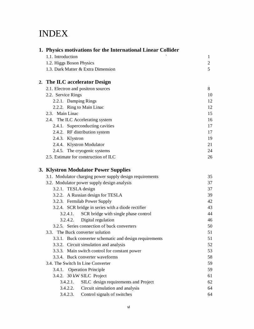
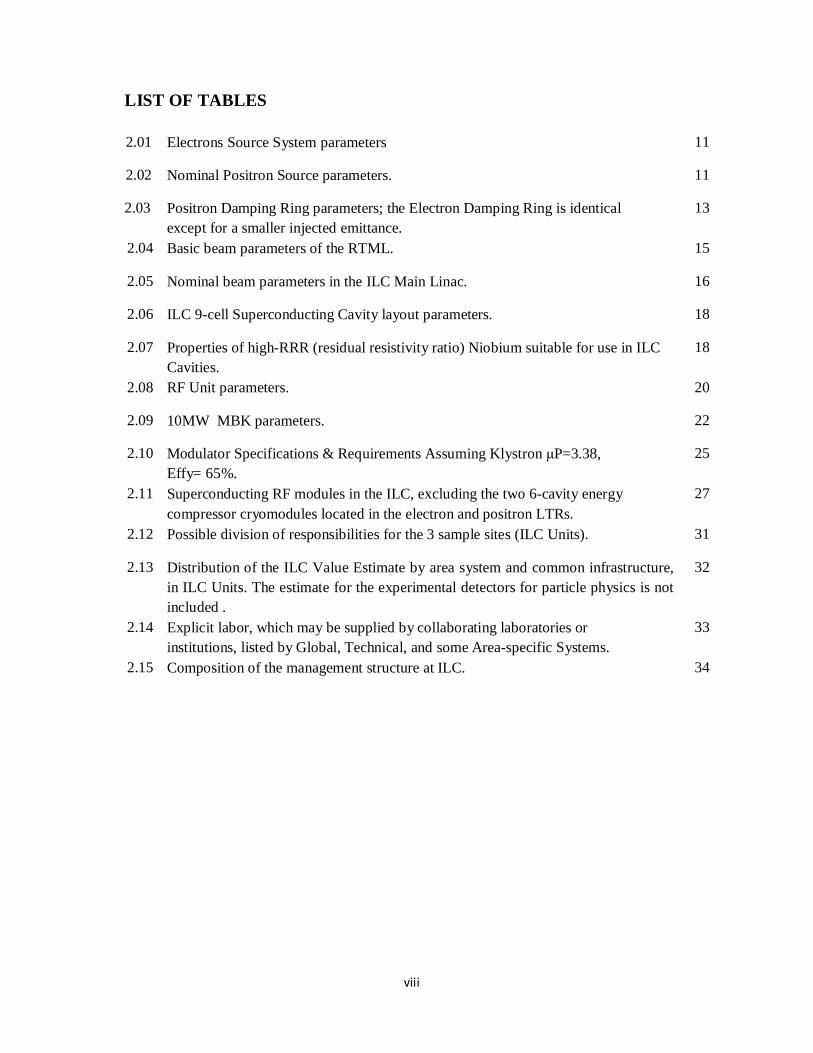
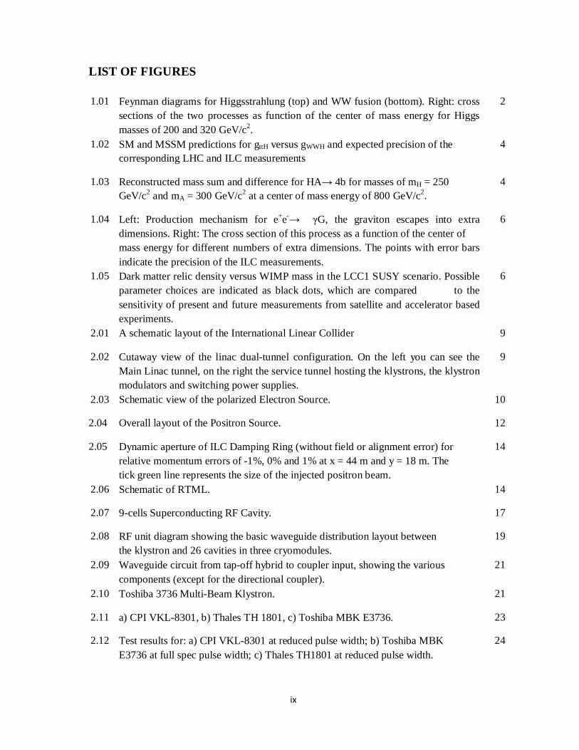
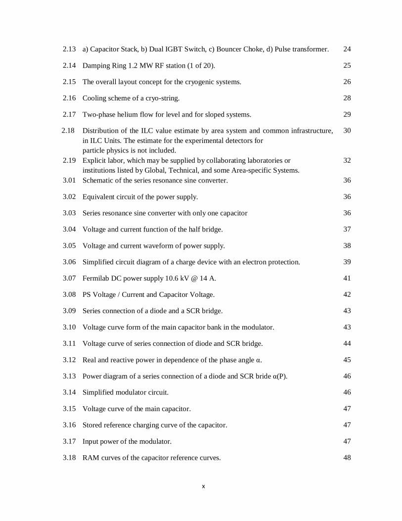