Embed Size (px)
Citation preview
Architectural, Numerical and Implementation
Issues in the VLSI Design of an Integrated
CORDIC-SVD Processor
Kishore Kota
Abstract
The Singular Value Decomposition (SVD) is an important matrix factorization with
applications in signal processing, image processing and robotics. This thesis presents
some of the issues involved in the design of an array of special-purpose processors
connected in a mesh, for fast real time computation of the SVD. The systolic array
implements the Jacobi method for the SVD. This involves plane rotations and inverse
tangent calculations and is implemented e�ciently in hardware using the COordinate
Rotation DIgital Computer (CORDIC) technique.
A six chip custom VLSI chip set for the processor was initially developed and
tested. This helped identify several bottlenecks and led to an improved design of
the single chip version. The single chip implementation incorporates several enhance-
ments that provide greater numerical accuracy. An enhanced architecture which
reduces communication was developed within the constraints imposed by VLSI. The
chips were fabricated in a 2:0� CMOS n-well process using a semicustom design style.
The design cycle for future chips can be considerably reduced by adopting a sym-
bolic layout style using high-level VLSI tools such as Octtools from the University of
California, Berkeley.
ii
Previous architectures for CORDIC processors provided logn bits to guard n bits
from truncation errors. A detailed error analysis of the CORDIC iterations indicates
that extra guard bits are required to guarantee n bits of precision. In addition,
normalization of the input values ensures greater accuracy in the calculations using
CORDIC. A novel normalization scheme for CORDIC which has O(n1:5) area complex-
ity as opposed to O(n2) area it would take if this were implemented using conventional
hardware, is described.
Data dependencies in the array allow only a third of the processors to be active
at any time. Several timing schemes which improve the utilization by overlapping
communication and computation are developed and evaluated. It is shown that it is
possible to e�ectively utilize all the idle time in the array by concurrently computing
the left and right singular vectors along with the singular values. Future versions of
the processor can implement these schemes.

Acknowledgments
Special thanks are due to Dr. Joe Cavallaro for being the motivation and a constant
driving force behind this work. I am especially thankful to him for being a good
friend and just being there when I needed him most. I would also like to thank Dr.
John Bennett and Dr. Peter Varman for serving on the committee and having the
patience to deal with me.
My friend and constant companion \�o" Hemkumar deserves special praise for
all those enlightening discussions and valuable comments, which on more than one
occasion prevented me from taking the wrong decisions. Thanks are due to my
roommate, Raghu, for his constant, but often futile e�orts at waking me up. But for
him I would have slept through the entire semester without a care. Thanks to the
Common Pool for allowing me to work through even the most di�cult times without
compromising on the food. Special thanks to my o�ce-mates Jay Greenwood and
Jim Carson. The o�ce would not be half as lively without them.
Finally I am eternally indebted to my mother and father. Even when they are
halfway across the world, nothing is possible without their blessings.

To my Grandfather,
For his one statement that has been the driving force through the years:
\. . . hope for the best, but be prepared for the worst . . . "

Contents
Abstract i
Acknowledgments iii
List of Tables viii
List of Illustrations ix
1 Introduction 1
1.1 Systolic Arrays for SVD . . . . . . . . . . . . . . . . . . . . . . . . . 2
1.2 Contributions of the thesis . . . . . . . . . . . . . . . . . . . . . . . . 3
1.3 Overview of the thesis . . . . . . . . . . . . . . . . . . . . . . . . . . 3
2 SVD Array Architecture 5
2.1 Introduction . . . . . . . . . . . . . . . . . . . . . . . . . . . . . . . . 5
2.2 The SVD-Jacobi Method . . . . . . . . . . . . . . . . . . . . . . . . . 6
2.3 Direct 2-Angle Method . . . . . . . . . . . . . . . . . . . . . . . . . . 8
2.4 Architecture for 2� 2 SVD . . . . . . . . . . . . . . . . . . . . . . . . 12
3 CORDIC Techniques 14
3.1 Introduction . . . . . . . . . . . . . . . . . . . . . . . . . . . . . . . . 14
3.2 CORDIC Algorithms . . . . . . . . . . . . . . . . . . . . . . . . . . . 15
3.3 CORDIC Operation in the Circular Mode . . . . . . . . . . . . . . . 16
3.3.1 CORDIC Z-Reduction . . . . . . . . . . . . . . . . . . . . . . 19
v

vi
3.3.2 CORDIC Y-Reduction . . . . . . . . . . . . . . . . . . . . . . 20
3.3.3 Modi�ed Y-Reduction for the SVD processor . . . . . . . . . . 22
3.4 Scale Factor Correction . . . . . . . . . . . . . . . . . . . . . . . . . . 23
3.5 Error Analysis of CORDIC Iterations . . . . . . . . . . . . . . . . . . 23
3.6 Error Analysis of CORDIC Z-Reduction . . . . . . . . . . . . . . . . 25
3.6.1 Error Introduced by X and Y Iterations . . . . . . . . . . . . 26
3.6.2 Error Introduced by Z Iterations . . . . . . . . . . . . . . . . 28
3.6.3 E�ects of perturbations in � . . . . . . . . . . . . . . . . . . . 29
3.7 Error Analysis of CORDIC Y-Reduction . . . . . . . . . . . . . . . . 30
3.7.1 Error Introduced by X and Y Iterations . . . . . . . . . . . . 31
3.7.2 Error Introduced by Z Iterations . . . . . . . . . . . . . . . . 32
3.7.3 Perturbation in the Inverse Tangent . . . . . . . . . . . . . . 32
3.8 Normalization for CORDIC Y-Reduction . . . . . . . . . . . . . . . . 33
3.8.1 Single Cycle Normalization . . . . . . . . . . . . . . . . . . . . 35
3.8.2 Partial Normalization . . . . . . . . . . . . . . . . . . . . . . . 36
3.8.3 Choice of a Minimal Set of Shifts . . . . . . . . . . . . . . . . 39
3.8.4 Cost of Partial Normalization Implementation . . . . . . . . . 43
3.9 Summary . . . . . . . . . . . . . . . . . . . . . . . . . . . . . . . . . 43
4 The CORDIC-SVD Processor Architecture 46
4.1 Introduction . . . . . . . . . . . . . . . . . . . . . . . . . . . . . . . . 46
4.2 Architecture of the Prototype . . . . . . . . . . . . . . . . . . . . . . 46
4.2.1 Design of the XY-Chip . . . . . . . . . . . . . . . . . . . . . . 48
4.2.2 Design of the Z-Chip . . . . . . . . . . . . . . . . . . . . . . . 50
4.2.3 Design of the Intra-Chip . . . . . . . . . . . . . . . . . . . . . 50
4.2.4 Design of the Inter-Chip . . . . . . . . . . . . . . . . . . . . . 54

vii
4.3 The CORDIC Array Processor Element . . . . . . . . . . . . . . . . . 55
4.4 Issues in Loading the Array . . . . . . . . . . . . . . . . . . . . . . . 60
4.4.1 Data Loading in CAPE . . . . . . . . . . . . . . . . . . . . . . 61
5 Architectures to Improve Processor Utilization 64
5.1 Introduction . . . . . . . . . . . . . . . . . . . . . . . . . . . . . . . . 64
5.2 Architecture for Systolic Starting . . . . . . . . . . . . . . . . . . . . 65
5.3 Architecture for fast SVD . . . . . . . . . . . . . . . . . . . . . . . . 70
5.4 Architecture for Collection of U and V Matrices . . . . . . . . . . . . 73
6 VLSI Implementation Issues 75
6.1 Design Methodology . . . . . . . . . . . . . . . . . . . . . . . . . . . 75
6.2 Reducing Skews in Control Signals . . . . . . . . . . . . . . . . . . . 78
6.3 Design of an Adder . . . . . . . . . . . . . . . . . . . . . . . . . . . . 79
6.4 Testing . . . . . . . . . . . . . . . . . . . . . . . . . . . . . . . . . . . 80
7 Conclusions 85
7.1 Summary . . . . . . . . . . . . . . . . . . . . . . . . . . . . . . . . . 85
7.2 Future Work . . . . . . . . . . . . . . . . . . . . . . . . . . . . . . . . 87
Bibliography 88

Tables
2.1 Parallel Ordering . . . . . . . . . . . . . . . . . . . . . . . . . . . . . 8
3.1 CORDIC Functionality in the Circular Mode . . . . . . . . . . . . . . 19
3.2 Total Shifts Using a Novel Normalization Scheme . . . . . . . . . . . 41
3.3 Summary and Comparison of Error Analysis . . . . . . . . . . . . . . 44
6.1 A list of some of the problems in the 6-chip prototype . . . . . . . . . 81
6.2 Breakdown of clock cycles for the various sub-tasks in the 6-chip
prototype . . . . . . . . . . . . . . . . . . . . . . . . . . . . . . . . . 83
6.3 Breakdown of clock cycles for the various sub-tasks in CAPE . . . . . 83
viii

Illustrations
2.1 The Brent-Luk-Van Loan SVD Array . . . . . . . . . . . . . . . . . . 9
2.2 Snapshots of Brent-Luk-Van Loan SVD Array . . . . . . . . . . . . . 11
3.1 Rotation of a vector . . . . . . . . . . . . . . . . . . . . . . . . . . . 17
3.2 Implementation of the CORDIC Iterations in Hardware . . . . . . . . 18
3.3 Rotation of a vector in Y-Reduction . . . . . . . . . . . . . . . . . . . 21
3.4 Error in Y-Reduction Without Normalization . . . . . . . . . . . . . 34
3.5 Algorithm to Invoke Modi�ed CORDIC Iterations . . . . . . . . . . . 40
3.6 Implementation of the CORDIC Iterations in Hardware . . . . . . . . 41
3.7 Error in Y-Reduction With Partial Normalization . . . . . . . . . . . 42
4.1 Block Diagram of the 6-chip Prototype CORDIC-SVD Processor . . . 47
4.2 Die Photograph of the XY-Chip . . . . . . . . . . . . . . . . . . . . . 49
4.3 Die Photograph of the Z-Chip . . . . . . . . . . . . . . . . . . . . . . 51
4.4 Block Diagram of the Intra-Chip . . . . . . . . . . . . . . . . . . . . 52
4.5 Die Photograph of the Intra-Chip . . . . . . . . . . . . . . . . . . . . 53
4.6 Block Diagram of Inter-Chip . . . . . . . . . . . . . . . . . . . . . . . 55
4.7 Die Photograph of the Inter-Chip . . . . . . . . . . . . . . . . . . . . 56
4.8 Internal Architecture of CAPE . . . . . . . . . . . . . . . . . . . . . . 58
ix

x
4.9 A Combined DSP-VLSI Array for Robotics . . . . . . . . . . . . . . . 62
5.1 Interconnection of Control Signals for Systolic Starting . . . . . . . . 66
5.2 Interconnection of Data Lines for Systolic Starting . . . . . . . . . . . 67
5.3 Snapshots of a Systolic Starting scheme . . . . . . . . . . . . . . . . . 69
5.4 Hardware Required for Fast SVD . . . . . . . . . . . . . . . . . . . . 71
5.5 Snapshots of an Array Computing U and V . . . . . . . . . . . . . . 73
6.1 Plot of the completed Single Chip Implementation . . . . . . . . . . . 77
6.2 Clock Generation with Large Skew . . . . . . . . . . . . . . . . . . . 78
6.3 Clock Generation with Small Skew . . . . . . . . . . . . . . . . . . . 78

Chapter 1
Introduction
Rapid advances made in VLSI and WSI technologies have led the way to an entirely
di�erent approach to computer design for real-time applications, using special-purpose
architectures with custom chips. By migrating some of the highly compute-intensive
tasks to special-purpose hardware, performance which is typically in the realm of
supercomputers, can be obtained at only a fraction of the cost. High-level Computer-
Aided Design (CAD) tools for VLSI silicon compilation, allow fast prototyping of
custom processors by reducing the tedium of VLSI design. Special-purpose architec-
tures are not burdened by the problems associated with general computers and can
map the algorithmic needs of a problem to hardware. Extensive parallelism, pipelin-
ing and use of special arithmetic techniques tailored for the speci�c application lead
to designs very di�erent from conventional computers.
Systolic and wavefront arrays form a class of special-purpose architectures that
hold considerable promise for real-time computations. Systolic arrays are character-
ized by \multiple use of each data item, extensive concurrency, a few types of simple
cells and a simple and regular data and control ow between neighbors" [21]. Systolic
arrays typically consist of only a few types of simple processors, allowing easy proto-
typing. The near-neighbor communication associated with systolic arrays results in
short interconnections that allow higher operating speeds even in large arrays. Thus,
systolic arrays o�er the potential for scaling to very large arrays. Numerical problems
1

2
involving large matrices bene�t from this property of systolic arrays.
Many real-time signal processing, image processing and robotics applications re-
quire fast computations involving large matrices. The high throughput required in
these applications can in general, be obtained only through special-purpose archi-
tectures. A computationally complex numerical problem, which has evoked a lot of
interest is the Singular Value Decomposition (SVD) [15]. It is generally acknowl-
edged that the SVD is the only generally reliable method for determining the rank
of a matrix numerically. Solutions to the complex problems encountered in real-time
processing, which use the SVD, exhibit a high degree of numerical stability. SVD tech-
niques handle rank de�ciency and ill-conditioning of matrices elegantly, obviating the
need for special handling of these cases. The SVD is a very useful tool, for example,
in analyzing data matrices from sensor arrays for adaptive beamforming [30], and low
rank approximations to matrices in image enhancement [2]. The wide variety of ap-
plications for the SVD coupled with its computational complexity justify dedicating
hardware to this computation.
1.1 Systolic Arrays for SVD
The SVD problem has evoked a lot of attention in the past decade. Numerous archi-
tectures and algorithms were proposed for computing the SVD in an e�cient manner.
The Hestenes' method using Jacobi transformations has been a popular choice among
researchers, due to the concurrency it allows in the computation of the SVD. Numerous
algorithms and architectures for the SVD were proposed by Luk [24, 26, 25, 23]. Brent,
Luk and Van Loan [5] presented an expandable square array of simple processors to
compute the SVD. A processor architecture for the Brent, Luk and Van Loan array,
using CORDIC techniques, was presented by Cavallaro [8].

3
1.2 Contributions of the thesis
A detailed study of the numerical accuracy of �xed-point CORDICmodules is provided
in this thesis. This analysis indicates a need to normalize the values for CORDIC Y-
reduction in order to achieve meaningful results. A novel normalization scheme for
�xed-point CORDIC Y-reduction that reduces the hardware complexity is developed.
This thesis is chie y concerned with the issues relating to the VLSI implemen-
tation of the CORDIC-SVD array proposed by Cavallaro. Many of the lower-level
architectural issues that are not relevant at the higher levels assume a new signi�-
cance when trying to implement the array. Elegant solutions have been found for all
the problems encountered in the design process.
An integrated VLSI chip to implement the 2 � 2 SVD processor element, which
serves as the basic unit of the SVD array, has been designed. A new internal archi-
tecture has been developed within the constraints imposed by VLSI.
Numerous array architectures that improve on the previous architectures were
developed as part of this research. These schemes can used in future implementations
as improvements to the current design.
1.3 Overview of the thesis
Chapter 2 presents the SVD algorithm and the array proposed by Brent, Luk and Van
Loan [5]. A discussion of the CORDIC-SVD processor is also provided. Chapter 3
reviews the CORDIC arithmetic technique and then presents an improved analysis
of the numerical accuracy of �xed-point CORDIC. Chapter 4 presents the improve-
ments made to the architecture of the single chip VLSI implementation of the SVD
processor over the various sub-units that constitute the prototype SVD processor.
Chapter 5 presents improvements to the array architecture and the impact of these

4
on the processor design. These improvements include schemes for systolic starting
and architectures that reduce idle time in the array, to achieve higher throughput.
Chapter 2
SVD Array Architecture
2.1 Introduction
This chapter introduces the principles that govern the e�cient computation of the
Singular Value Decomposition (SVD) in a parallel array. A major portion of the work
in this thesis is based on the Brent, Luk and Van Loan [5] array for computing the
SVD. Later sections of this chapter provide insight into the operation of this array.
The SVD has proved to be an important matrix decomposition with theoretical
and practical signi�cance. The canonical representation of a matrix provided by the
SVD is very useful in determining its properties. The SVD [15] of a p� p matrix A is
de�ned as
A = U�V T; (2.1)
where,
U and V are orthogonal matrices of dimension p� p, and
� = diag(�1; �2; � � � ; �p) is a diagonal matrix of singular values.The columns of U and V are called the left and the right singular vectors respectively.
The SVD is a compute intensive operation requiring O(p3) time on a sequential
computer. For example, the SVD of an 8� 8 matrix on a SUN 3/60 requires about
1 second of CPU time using LINPACK [12], a library of linear algebra routines. A
typical real-time application, the inverse kinematics engine of a robot, requires the
5
6
computation of the SVD of an 8� 8 matrix every 400�sec. This is precisely the class
of applications where the use of dedicated arrays is attractive. With a square array
of processors it is possible to reduce the time complexity for the SVD to O(p log p).
2.2 The SVD-Jacobi Method
The Jacobi method to compute the SVD is a popular algorithm for parallel imple-
mentation, due to the concurrency it introduces to the problem. The algorithm is
based on the use of orthogonal transformations, called Jacobi Rotations 1 to selec-
tively reduce a given matrix element to zero. A Jacobi rotation by an angle � in the
ij plane, is a p� p matrix, J(i; j; �), where,
jaa = 1 8 (a 6= i; j) ;
jii = cos � ; jij = sin � ;
jji = � sin � ; jjj = cos � ;
(2.2)
and all other jab = 0:
Intuitively, a Jacobi rotation is an identity matrix with four of its elements replaced
by a vector rotation matrix as shown below:
J(i; j; �) =
266666666666664
1 � � � 0 � � � 0 � � � 0...
. . ....
......
0 � � � cos � � � � sin � � � � 0...
.... . .
......
0 � � � � sin � � � � cos � � � � 0...
......
. . ....
0 � � � 0 � � � 0 � � � 1
377777777777775
i
j
i j
(2.3)
The parameters i and j select the matrix element that is to be reduced to zero,
while the parameter � is computed using a few matrix elements. Since very few
1also called Givens Rotations or simply plane rotations

7
matrix elements are required to compute the entire transformation, local computation
is possible by storing all the required data in the registers of a single processor. In
addition, pre-multiplication with a Jacobi rotation matrix, called left-sided rotation,
modi�es only the ith and jth rows, while a right-sided rotation a�ects only the ith
and jth columns. This introduces concurrency, since computations which use the
unmodi�ed data elements can be performed in parallel.
The SVD algorithm consists of a sequence of orthogonal 2 Jacobi transformations,
chosen to diagonalize the given matrix. The algorithm to compute the SVD is iterative
and can be written as
A0 = A; (2.4)
Ak+1 = UTk AkVk = Jk(i; j; �l)
TAkJk(i; j; �r): (2.5)
Appropriate choice of the 2-sided rotations can force Ak to converge to the diagonal
matrix of singular values �. The matrix of left singular vectors is obtained as a
product of the left rotations Uk, while the matrix of right singular vectors is obtained
as a product of the right-sided rotations. At each iteration k, a left rotation of �l and
a right rotation of �r in the plane ij are chosen to reduce the two o�-diagonal elements
aij and aji of Ak to zero. A sweep consists of n(n� 1)=2 iterations that reduce every
pair of o�-diagonal elements to zero. Several sweeps are required to actually reduce
the initial matrix to a diagonal matrix. The sequence, in which the o�-diagonal pairs
are annihilated within each sweep is chosen apriori according to some �xed ordering.
Forsythe-Henrici [14] proved that the algorithm converges for the cyclic-by-rows and
cyclic-by-columns ordering. However, these orderings do not allow decoupling of
successive iterations, thereby restricting the parallelism achievable. Brent and Luk [4]
introduced the parallel ordering that does not su�er from this drawback.
2A matrix is orthogonal when its transpose equals the inverse

8
(1,2) (3,4) (5,6) (7,8)(1,4) (2,6) (3,8) (5,7)(1,6) (4,8) (2,7) (3,5)(1,8) (6,7) (4,5) (2,3)(1,7) (8,5) (6,3) (4,2)(1,5) (7,3) (8,2) (6,4)(1,3) (5,2) (7,4) (8,6)
Table 2.1: Parallel Ordering data exchange with 8 elements. This is the
ordering used when eight chess players have to play a round-robin tour-
nament, each player playing one game a day.
An iteration that annihilates a11 and a22 does not a�ect any of the terms required
for annihilating a33 and a44, allowing the two sets of rotation angles to be computed
concurrently. Thus parallel ordering allows decoupling of the computation of the
Jacobi transformations of all the iterations in a single row of the ordering (Table 2.1).
Brent, Luk and Van Loan [5] proposed a square array of processors based on this
scheme. The ordering has an additional property that it requires only near-neighbor
communication in an array and is hence amenable to systolic implementation.
2.3 Direct 2-Angle Method
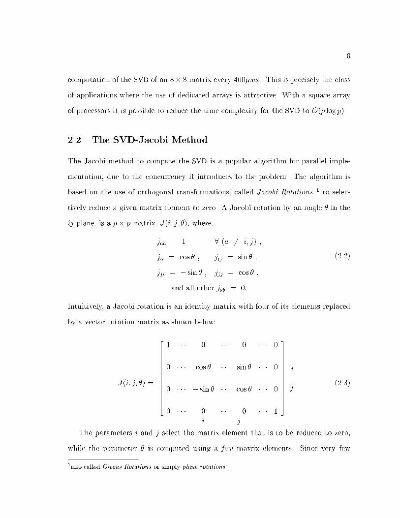
The Brent, Luk and Van Loan systolic array [5] consists of a p=2 � p=2 array of
processors (Figure 2.1) to compute the SVD of a p�p matrix. The matrix dimension,p, is assumed to be even. Each processor stores a 2� 2 submatrix and has the ability
to compute the SVD of a 2� 2 matrix. The special structure of the Jacobi rotation
matrix allows computing the angles for a p� p two-sided rotation in terms of a basic
2� 2 rotation. The application of the transformation on a p� p matrix can also be
expressed as a set of 2� 2 transformations. Thus the 2� 2 SVD forms the basic step
for the p� p SVD.
9
A B
C D
θ l
θr
θr
θr
θr
θr
θr
θr
θr
θr
θr
θr
θr
θr
θr
θr
θr
θr
θr
θr
θr
θ lθ l θ l
θ l θ l
θ l θ lθ l
θ lθ l θ l
θ lθ lθ lθ lθ lθ l
θ lθ l
θ lθ lθ l
θ l
A B
C D
A B
C D
A B
C D
A B
C D
A B
C D
A B
C D
A B
C D
A B
C D
A B
C D
A B
C D
A B
C D
A B
C D
A B
C D
A B
C D
A B
C D
P00 P01 P02 P03
P10 P11 P12 P13
P20 P21 P22 P23
P30 P31 P32 P33
Figure 2.1: The Brent-Luk-Van Loan SVD Array for Computing the SVD
of an 8� 8 Matrix

10
A 2� 2 SVD can be described as
R(�l)T
24 a b
c d
35R(�r) =
24 1 0
0 2
35 ; (2.6)
where �l and �r are the left and right rotation angles, respectively. The rotation
matrix is
R(�) =
24 cos � sin �
� sin � cos �
35 ; (2.7)
and the input matrix is
M =
24 a b
c d
35 :
The angles �l and �r necessary to diagonalize the matrix M can be shown to be
the inverse tangents of the data elements of M :
�r + �l = tan�1"c+ b
d� a
#;
�r � �l = tan�1"c� b
d+ a
#(2.8)
The left and right rotation angles in equation 2.5 can be computed using the
equations 2.8 on a 2� 2 matrix formed by
24 aii aij
aji ajj
35. It may be noted that the p=2
diagonal processors store precisely the matrices required for p=2 successive iterations,
corresponding to a single row of parallel ordering in Table 2.1. All the transformations
that annihilate the o�-diagonal elements in the diagonal processors are independent
and hence can be computed in parallel. An update of the entire array requires the left
angles to be propagated from a diagonal processor to all the processors on the same
row, and the right angle to be propagated to all the processors on the same column.
This propagation is systolic. The update of the matrix is followed by a permutation
of the rows and the columns of the matrix according to the parallel ordering. An 8-
connected mesh is required to perform this data exchange. The permutation results in
the next set of sub-matrices, required to compute the new set of angles, to be formed

11
1
1
1
1
1
1
1
1
1
1
1
1
1
1
2
1
1
2
2
2
2
2
2
2
2
2
2
2
2
2
Figure 2.2: Snapshots of the Brent-Luk-Van Loan SVD Array Showing
Diagonal Waves of Activity
at the diagonal processors. Since the diagonal processors require data only from their
diagonal neighbors, new computation can start as soon as these neighbors complete
their portion of the computation. Thus, the updates of the matrix, corresponding
to separate iterations in equation 2.5 are pipelined. This leads to diagonal waves of
activity originating at the main diagonal and propagating outwards. This is shown
in Figure 2.2. The various steps in the operation of this array are listed below:
� The p=2 diagonal processors compute the required transformation angles using
the 2� 2 sub-matrix stored in them.
� Each diagonal processor propagates the left angle, which it computed, to its east
and west neighbor. Similarly the right rotation angles are propagated north and
south.

12
� The non-diagonal processors receive the left and right angles and apply the 2-
sided transformation to their sub-matrices. After the computation, they forward
the left and right rotation angles to the processor next in the row or column.
� Processor P22 in Figure 2.1 receives its next set of data elements from processors
P11, P33, P13 and P31. Hence, it has to wait till processors P31 and P13 �nish
their computations. Similarly, all the other diagonal processors need to wait
for their diagonal neighbors to complete the transformations before exchanging
data. Exchange of data in di�erent parts of the array is staggered in time.
� After the data exchange, a new set of angles is computed by the diagonal pro-
cessors and the same sequence of operations is repeated.
Each diagonal processor requires (p-1) iterations to complete a sweep. The number
of sweeps required for convergence is O(log p). For most matrices up to a size of
100 � 100, the algorithm has been observed to converge within 10 sweeps. Since
each iteration for a diagonal processor is completed in constant time, the total SVD
requires O(p log p).
2.4 Architecture for 2� 2 SVD
The array proposed by Brent, Luk and Van Loan was converted into an architecture
suitable for VLSI implementation by Cavallaro and Luk [8]. By using CORDIC arith-
metic, a simple architecture suitable for systolic implementation was developed. The
basic functionality required in each processor is:
� Ability to compute inverse tangents is required for the computation of the 2-
sided transformations from matrix data,

13
� Ability to perform 2-sided rotations of a 2 � 2 matrix that is required when
performing the transformation,
� Control to perform the parallel ordering data exchange.
CORDIC allows e�cient implementation of the required arithmetic operations in
hardware. Chapter 3 discusses the CORDIC algorithm in depth. The architecture of
the individual processor element is discussed in Chapter 4.

Chapter 3
CORDIC Techniques
3.1 Introduction
In a special-purpose VLSI processor it is not necessary to include a general purpose
Arithmetic and Logic Unit (ALU). An e�cient design with optimal area and time
complexity can be obtained by using special arithmetic techniques that map the
desired computations to simpli�ed hardware. The CORDIC technique allows e�cient
implementation of functions, like vector rotations and inverse tangents, in hardware.
These constitute the principal computations in the SVD algorithm. Additional ALU
operations (addition, subtraction and divide-by-2) required for the SVD are more
basic operations and can reuse the adders and shifters that constitute the CORDIC
modules.
The Coordinate Rotation Digital Computer (CORDIC) technique was initially de-
veloped by Volder [35] as an algorithm to solve the trignometric relationships that
arise in navigation problems. Involving only a �xed sequence of additions or subtrac-
tions, and binary shifts, this scheme was used to quickly and systematically approx-
imate the value of a trignometric function or its inverse. This algorithm was later
uni�ed for several elementary functions by Walther [36]. The algorithm has been used
extensively in a number of calculators [16] to perform multiplications, divisions, to
calculate square roots, to evaluate sine, cosine, tangent, arctangent, sinh, cosh, tanh,
arctanh, ln and exp functions, and to convert between binary and mixed radix num-
14

15
ber systems [10].
3.2 CORDIC Algorithms
A variety of functions are computed in CORDIC by approximating a given angle
in terms of a sequence of �xed angles. The algorithm for such an approximation
is iterative and always converges in a �xed number of iterations. The basic result
of CORDIC concerns the convergence of the algorithm and is discussed in depth by
Walther [36]. The convergence theorem states the conditions that a�ect convergence
and essentially gives an algorithm for such an approximation. The theorem is restated
here. Walther [36] gives the proof for this theorem.
Theorem 3.1 (Convergence of CORDIC) Suppose
'0 � '1 � '2 � � � � � 'n�1 > 0;
is a �nite sequence of real numbers such that
'i �n�1Xj=i+1
'j + 'n�1; for 0 � i � n� 1;
and suppose r is a real number such that
jrj �n�1Xj=0
'j
If s0 = 0, and si+1 = si + �i'i, for 0 � i � n� 1, where
�i =
8>><>>:
1; if r � si
�1; if r < si;
then,
jr � skj �n�1Xj=k
'j + 'n�1; for 0 � k � n� 1;
and so in particular jr � snj < 'n�1.

16
If 'is represent angles, the theorem provides a simple algorithm for approximating
any angle r, in terms of a set of �xed angles 'i, with a small error 'n�1. The versatility
of the CORDIC algorithm allows its use in several di�erent modes: linear, circular
and hyperbolic. The principal mode of interest in the CORDIC-SVD processor is the
circular mode of CORDIC, due to its ability to compute vector rotations and inverse
tangents e�ciently.
3.3 CORDIC Operation in the Circular Mode
The anticlockwise rotation of a vector [ ~xi; ~yi ]T through an angle �i (Figure 3.1) is
given by 24 ~xi+1~yi+1
35 =
24 cos�i sin�i
� sin�i cos�i
3524 ~xi~yi
35 : (3.1)
The same relation can be rewritten as24 ~xi+1 sec�i
~yi+1 sec�i
35 =
24 1 tan�i
� tan�i 1
3524 ~xi~yi
35 : (3.2)
All computations in the circular mode of CORDIC involve a �xed number of iter-
ations, which are similar to equation 3.2, but for a scaling,
xi+1 = xi + �iyi tan�i (3.3)
yi+1 = yi � �ixi tan�i; (3.4)
where xi and yi are states of variables x and y at the start of the ith iteration,
0 � i < n, and �i 2 f�1;+1g. The values xn and yn are the values obtained at the
end of the CORDIC iterations and di�er from the desired values ~xn and ~yn due to a
scaling as shown in Figure 3.1. Along with the x and y iterations, iterations of the
form
zi+1 = zi + �i�i (3.5)

17
0 0x ,( )y~ ~
xn ,( ) y n~ ~
nx ,( )yn
α i
x
y
0x~ nx~ nx
0y~
ny~ny
Figure 3.1: Rotation of a vector
are performed on a variable z to store di�erent states of an angle. The angles �i are
chosen to be tan�1(2�i), which reduces equation 3.3 and equation 3.4 to
xi+1 = xi + �iyi2�i (3.6)
yi+1 = yi � �ixi2�i: (3.7)
These iterations, called the x and the y iterations, can be implemented as simple
additions or subtractions, and shifts. The angles �i are stored in a ROM , allowing the
z iterations, given by equation 3.5, to be implemented as additions or subtractions.
The actual hardware required to implement these iterations in hardware is shown in
Figure 3.2.
Rotation of a vector through any angle � is achieved by decomposing the angle
as a sum of �is, using the CORDIC convergence theorem, and rotating the initial
vector through this sequence of angles. Di�erent functions are implemented by a
di�erent choice of �i at each iteration. If �i is chosen to force the initial z0 to 0, it

18
ControlUnitPLA
x
y
z
AngleMemory
+ / -
+ / -
+ / -
2-j
Shift
Shift
Figure 3.2: Implementation of the CORDIC Iterations in Hardware

19
Operation Initial Valuesfor Variables
Final values for variablesFunctionsComputed
Z-Reductionx0 = ~x0
y0 = ~y0
z0 = �
xn = (x0 cos � + y0 cos �)=Kn
yn = (�x0 sin � + y0 cos �)=Kn
zn = 0
VectorRotations,sine, cosine
Y-Reductionx0 = ~x0
y0 = ~y0
z0 = �
xn =qx2
0+ y
2
0=Kn
yn = 0
zn = � = tan�1�y0
x0
� InverseTangents
Table 3.1: CORDIC Functionality in the Circular Mode
is termed Rotation or Z-reduction. This is used to perform e�cient vector rotations
given an initial angle. A choice of �is to reduce the initial y0 to 0 is called Vectoring
orY-reduction. Iterations of this form allow the computation of the inverse tangent
function. Table 3.1 summarizes the various operations performed in the CORDIC
circular mode, as they pertain to the SVD processor.
3.3.1 CORDIC Z-Reduction
Given an initial vector [~x0; ~y0]T = [x0; y0]
T and an angle z0 = �, through which to
rotate, the rotated vector can be obtained by rotating the initial vector through a
sequence of �xed angles �i given by �i = tan�1(2�i). This results in the following
iterative equations
xi+1 = xi + �iyi2�i
yi+1 = yi � �ixi2�i
zi+1 = zi � �i�i; (3.8)
20
where,
�i = tan�1(2�i)
�i =
8>><>>:
1 if zi � 0
�1 if zi < 0.
Each iteration for xi and yi corresponds to either a clockwise or an anticlockwise
rotation of [xi; yi]T through the angle �i, and a scaling with sec(�i). The CORDIC
iterations for zi correspond to a decomposition of the initial angle in terms of a set
of �xed angles, �i, as given by Theorem 3.1.
After n iterations, the vector [xn; yn]T is a clockwise rotation of [x0; y0]
T through
an angle � and a scaling by 1=Kn. Figure 3.1 illustrates xn and yn scaled with respect
to the desired values ~xn and ~yn. This can be expressed as24 xnyn
35 =
24 cos � sin �
� sin � cos �
3524 x0=Kn
y0=Kn
35 ; (3.9)
where Kn, the constant scale factor, is given by equation 3.10,
Kn =n�1Yi=0
cos�i: (3.10)
This scale factor is independent of the actual �is chosen at each step, and converges
to � 0:607 for large n. A post-processing step is required to eliminate the scale factor.
An algorithm for scale-factor correction is described in Section 3.4. Z-reduction can
be used to compute the cosine and sine of the initial angle �, by choosing special cases
for the initial vector [x0; y0]T .
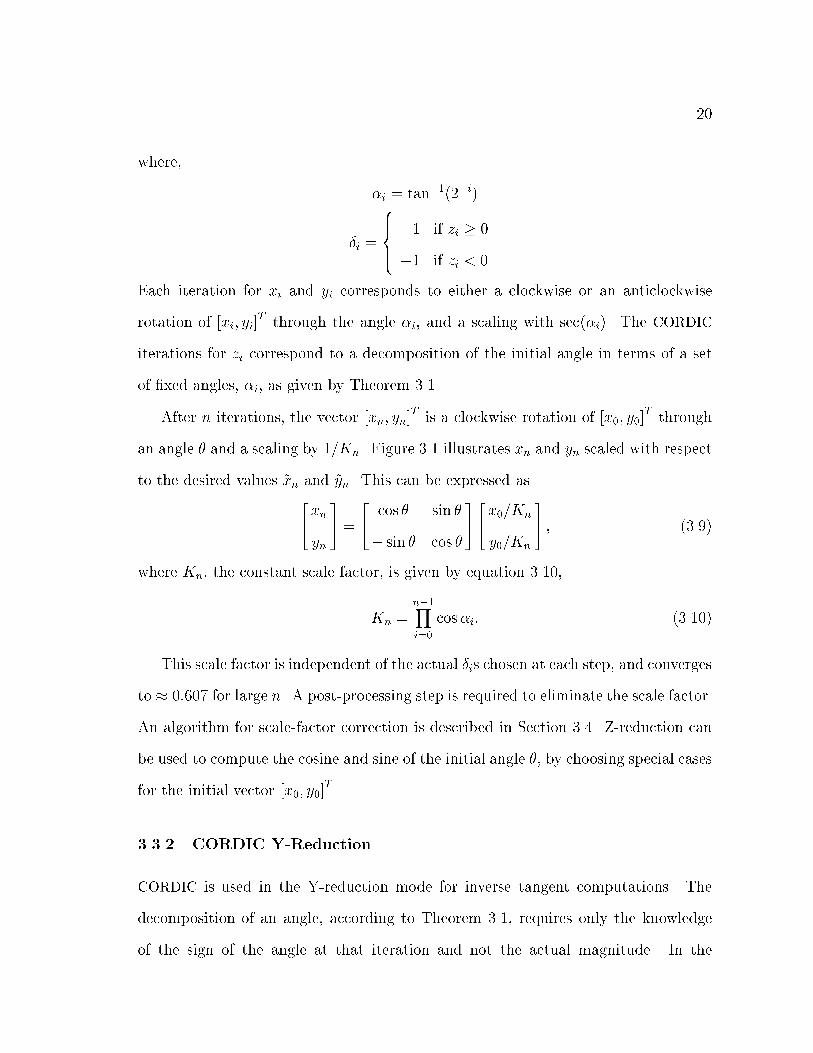
3.3.2 CORDIC Y-Reduction
CORDIC is used in the Y-reduction mode for inverse tangent computations. The
decomposition of an angle, according to Theorem 3.1, requires only the knowledge
of the sign of the angle at that iteration and not the actual magnitude. In the
21
ix ,( )y
i
x
y
α i
i+1 i+1(x , y )
tan ( y / x )i i
-1 xi+1
xi
yi
yi+1
Figure 3.3: Rotation of a vector in Y-Reduction
computation of tan�1(y0=x0), the same information is obtained from the y component
of the vector at each iteration. As shown in Figure 3.3, if �i > 0, yi > 0 and vice
versa. The function tan�1(y0=x0) is computed by rotating the initial vector through
successively smaller angles �i, the direction of rotation at each step chosen to reduce
the y-component of the vector to zero. The total angle, through which the vector
has been rotated is accumulated in the z-register. The CORDIC convergence theorem
forces the accumulated angle to within tan�1(2�n) of tan�1(y0=x0). Using the initial
values [~x0; ~y0]T = [x0; y0]
T and z0 = 0, the following CORDIC iterations can be used
to compute the value of tan�1(y0=x0):
xi+1 = xi + �iyi2�i
yi+1 = yi � �ixi2�i
zi+1 = zi + �i�i; (3.11)
22
where,
�i = tan�1(2�i);
�i =
8>><>>:
1 if yi � 0
�1 if yi < 0:(3.12)
After n iterations, xn =qx2
0 + y2
0=Kn, yn � 0 and zn = tan�1(y0=x0). If the
radiusqx2
0+ y
2
0is desired, a scale factor correction step is necessary. The �nal vector
(xn; yn) is the initial vector (x0; y0) rotated through tan�1(y0=x0) and scaled.
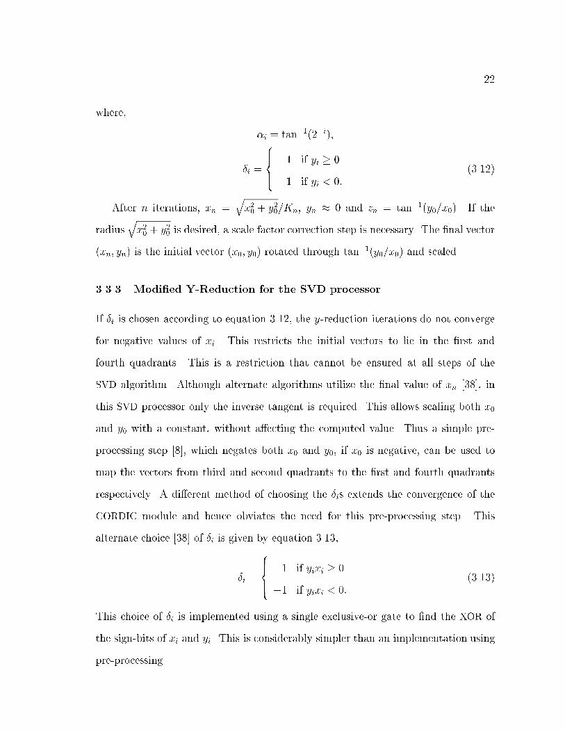
3.3.3 Modi�ed Y-Reduction for the SVD processor
If �i is chosen according to equation 3.12, the y-reduction iterations do not converge
for negative values of xi. This restricts the initial vectors to lie in the �rst and
fourth quadrants. This is a restriction that cannot be ensured at all steps of the
SVD algorithm. Although alternate algorithms utilize the �nal value of xn [38], in
this SVD processor only the inverse tangent is required. This allows scaling both x0
and y0 with a constant, without a�ecting the computed value. Thus a simple pre-
processing step [8], which negates both x0 and y0, if x0 is negative, can be used to
map the vectors from third and second quadrants to the �rst and fourth quadrants
respectively. A di�erent method of choosing the �is extends the convergence of the
CORDIC module and hence obviates the need for this pre-processing step. This
alternate choice [38] of �i is given by equation 3.13,
�i =
8>><>>:
1 if yixi � 0
�1 if yixi < 0:(3.13)
This choice of �i is implemented using a single exclusive-or gate to �nd the XOR of
the sign-bits of xi and yi. This is considerably simpler than an implementation using
pre-processing.

23
3.4 Scale Factor Correction
There have been numerous approaches to scale factor correction in the literature [36,
16, 1, 11]. Most approaches require special iterations of a form similar, but not
identical, to the CORDIC iterations. It is important to reduce the number of these
iterations to the minimum, since scale factor correction may be regarded as overhead.
Most scale factor correction algorithms approximate the value of Kn as
Yj2J
(1� 2j);
where J is a set of values obtained empirically. The cardinality of the set J is typically
at least n=4 and in some cases as large as n. An alternate algorithm (equation 3.14),
which is more regular and hence useful for di�erent values of n is applicable after two
complete CORDIC rotations. By the end of two CORDIC rotations, the variables xn
and yn are scaled by K2
n. The scheme [8] to eliminate the factor of K2
n requires only
dn=4e scale factor correction iterations after two CORDIC rotations of n iterations
each and, hence, is cheaper than the other scale factor correction algorithms,
2K2
n =Yj2J
(1� 2�2j); (3.14)
where J = f1; 3; 5; � � � ; 2dn=4e � 1g. The scale factor iterations are given by
xi+1 = xi � xi2�j
yi+1 = yi � yi2�j; (3.15)
where, j = 2; 6; 10 � � � ; 4dn=4e � 2. At the end of these iterations, the factor of 2 in
equation 3.14 is eliminated by a simple right shift.
3.5 Error Analysis of CORDIC Iterations
Any numerical scheme has to be resilient to truncation errors at every stage of com-
putation in order to justify its implementation in a computer. Error analysis is the

24
acid test to determine whether a numerical algorithm is suitable for implementation.
Many algorithms that are mathematically accurate, fail in the presence of truncation
errors. While �nite precision presents insurmountable problems to some algorithms,
it results in only a bounded error in some others. A detailed study of these errors is
necessary to interpret the results and guarantee a certain degree of accuracy.
Although CORDIC has been used previously, much of the analysis of its numerical
accuracy has been ad hoc. Walther [36] claimed that a precision of n bits can be
achieved if the internal representation used is n + log2n bits. This analysis neglects
any interaction between the various iterations and considers only the e�ect of the �nite
precision of the x and y data paths. Walther studied CORDIC for a oating-point
implementation and pointed out that it is necessary to use a normalized representation
to achieve this precision. Johnsson [18] attempted to obtain a closer bound on the
error caused by x and y iterations, while still neglecting the interaction between the
various iterations. This analysis showed that the internal representation of L bits
guarantees an accuracy of n bits, if,
L > n+ log2(2n� L� 3): (3.16)
This is again n + log2n bits internal representation to obtain the desired precision
of n bits. Both the analyses neglect the e�ect of the z iterations on the the x and y
iterations and vice versa.
A more detailed error analysis for �xed-point CORDIC modules is presented by
Duryea [13]. He shows that the error for Z-reduction is bounded as:
j~xn � xnj � 7
6n2�t1 + 2�(n�1) (3.17)
where, n is the number of iterations and t1 is the bit precision of x, y and z. In
addition, he shows that the error in the computed value of inverse tangent is:
j~�n � �nj � (n+ 1)2�t1 + 2�(n�1) (3.18)

25
This error bound, however, does not account for the e�ect of unnormalized x0 and
y0, which is the main source of error in Y-reduction.
An exact analysis of the various errors involved in CORDIC is presented in Sections
3.6 and 3.7. For a �nite number of iterations, CORDIC computes an approximate
value of the desired functions even with in�nite precision. Thus an error is inherently
associated with the computations. This error is usually very small. Additional errors
occur due to the �nite-precision representation of the di�erent variables. The analysis
presented in this thesis uses the following notation to represent the di�erent values
of the variables x, y and z:
� xi, yi, zi represent the actual values obtained due to CORDIC iterations, assum-
ing �nite-precision arithmetic in a real-world implementation of CORDIC,
� xi, yi, zi represent the values that will be obtained if the same CORDIC it-
erations that were performed in the previous case, are performed on numbers
represented with in�nite-precision,
� ~xi, ~yi, ~zi represent the values that should be obtained for the desired function
with in�nite precision, as mathematically de�ned.
3.6 Error Analysis of CORDIC Z-Reduction
Let the initial values for x, y and z be x0, y0, z0 = �. Each CORDIC iteration for x
and y is of the form,
xi+1 = xi + �iyi2�i
yi+1 = yi � �ixi2�i:
Finally after n iterations,
xn = (x0 cos�+ y0 sin�)=Kn (3.19)

26
yn = (y0 cos�� x0 sin�)=Kn; (3.20)
where,
Kn =n�1Yi=0
cos�i
�i = tan�1(2�i)
� =n�1Xi=0
�i�i: (3.21)
The sequence of �is is exactly the same as what would be obtained in a real-
world implementation of CORDIC, using the same initial conditions. The angle � is
an approximation of �. Since the x and y iterations implement a rotation through
tan�1 (2�i) by shifting the variables, they achieve a rotation through exactly �i. The
�nite-precision representation of xi and yi, however, causes a truncation error in their
computation. Let the actual values of xi and yi obtained at the end of each iteration
be xi; yi.
3.6.1 Error Introduced by X and Y Iterations
Suppose x and y are represented with t1 bits and x and y are interpreted as fractions,
without any loss of generality. Since the numbers are truncated after the right shift,
the addition and subtraction operations result in a truncation error not exceeding
2�t1. Accordingly,
x1 = x0 + �0y02�0 = x1
y1 = y0 + �0x02�0 = y1:
The second iteration results in a truncation error due to the right shift,
x2 = x1 + �1y12�1 + �x1 = x2 + �x1
y2 = y1 + �1x12�1 + �y1 = y2 + �y1;

27
where,
j�x1j; j�y1j < 2�t1 :
Using these values in the next iteration results in,
x3 = x2 + �2y22�2 + �x2
= x2 + �2y22�2 + (�x1 + �y1�22
�2) + �x2
= x3 + (�x1 + �y1�22�2) + �x2:
Continuing this for n iterations, we obtain
xn = xn + �x (3.22)
yn = yn + �y; (3.23)
where,
j�xj; j�yj < 2�t1 [1 + (1 + �(n�1)2�(n�1)) +
(1 + �(n�1)2�(n�1))(1 + �(n�2)2
�(n�2)) + � � �+
(1 + �(n�1)2�(n�1))(1 + �(n�2)2
�(n�2)) : : : (1 + �12�1)]
< 2�t1 [1 + (1 + 2�(n�1)) +
(1 + 2�(n�1))(1 + 2�(n�2)) + � � �+
(1 + 2�(n�1))(1 + 2�(n�2)) : : : (1 + 2�1)]
� 2�t1(n):
The upper bound is obtained by considering the maximum value for the right
hand side of the above relation, which occurs when all �i = +1. The sum of the
product terms is approximately n. Hence, the �nite precision representation of the x
and y causes an error in approximately logn bits.
28
3.6.2 Error Introduced by Z Iterations
Let �i be the �nite-precision approximation of �i, then assuming �xed point imple-
mentation,
�i = �i + �2i; j�2ij < 2�t2 ; (3.24)
where �i is assumed to be represented by t2 bits. The value �i is the actual value
of tan�1(2�i) stored in the ROM. The error in representation of the angle �i, due to
�nite precision is �2i.
Each iteration of CORDIC for the z variable is of the form
zi+1 = zi � �i�i:
The sequence of �is satis�es the conditions required by Theorem 3.1, in spite of the
errors, and hence causes the z iterations to converge. The absence of any shifting
in the z iterations implies exact arithmetic, since no bits are truncated. The only
deviation ofP�i�i from the angle � is a consequence of the CORDIC approximation.
Accordingly, from the convergence properties of CORDIC,
zn � �n�1;
z0 = � =n�1Xi=0
�i�i + ; j j � �n�1
Theorem 3.1 governs the maximum error possible in this expression to be less than
the smallest angle �n�1. Coupling the �nite-precision approximation error in the
representation of �i with this relation, gives a bound on the deviation of the angle �
from the desired angle �. The angle �, is the angle through which the vector [ x0; y0 ]T
is actually rotated. Using equations 3.21 and 3.24:
� =n�1Xi=0
�i�i �n�1Xi=0
�i�2i +
= ��n�1Xi=0
�i�2i + : (3.25)

29
Substituting the bounds on and �2i and choosing �i = �1, the error in the angle
j�� �j is,
j�� �j < �n�1 + n2�t2 = tan�1(2�(n�1)) + n2�t2 � 2�(n�1) + n2�t2 (3.26)
Equation 3.26 gives the error that could be caused in the z iterations in the worst
case.
3.6.3 E�ects of perturbations in �
Combining results from equations 3.19, 3.22, 3.25, a relation can be derived between
what we obtain, [xn; yn]T , and what we expect, [~xn; ~yn]
T . The expected values can be
expressed in terms of exact equations as,
~xn = (x0 cos � + y0 sin �)=Kn (3.27)
~yn = (y0 cos � � x0 sin �)=Kn: (3.28)
Assuming that the error �� = j�� �j is small, the error in ~xn and ~yn can be obtained
through di�erentiation as
@~xn@�
= (�x0 sin � + y0 cos �)=Kn = ~yn=Kn (3.29)
@~yn@�
= (�y0 sin � � x0 cos �)=Kn = �~xn=Kn: (3.30)
An approximation that can be made if the error in the angles is small is,
�~xn � @~xn@�
��
�~yn � @~yn@�
��:
Observing that the derivatives are always less than 1 yields,
j~xn � xnj < ��

30
j~yn � ynj < ��:
Substituting the maximum errors for ��, xn and yn, an upper bound on the actual
observed error is obtained:
j~xn � xnj; j~yn � ynj < (�n�1 + n2�t2) + �x
< (2�(n�1) + n2�t2) + (n)2�t1 : (3.31)
This error is bounded for all values of jx0j and jy0j. Hence, this error can be
eliminated by increasing the data-width to include extra bits as guard bits. The error
bound obtained here is nearly the same as that given by equation 3.17. However,
equation 3.31 separates the e�ects of the x, y iterations and the z iterations allowing
a study of di�erent components of the error.
For the prototype implementation, t1 = 15, t2 = 15 and n = 16. Thus the error is
given by,
Observed Error < (2�15 + (16) 2�15) + (16) 2�15
< (33) 2�15
The error predicted by this relation is pessimistic and may never occur in practice.
It is reasonable to include log232 = 5 guard bits to correct the error.
3.7 Error Analysis of CORDIC Y-Reduction
Let the initial values for x, y and z be x0, y0, z0 = 0. Each CORDIC iteration for x
and y is of the form,
xi+1 = xi + �iyi2�i
yi+1 = yi � �ixi2�i:

31
Finally after n iterations the equations yield,
xn = (x0 cos�+ y0 sin�)=Kn (3.32)
yn = (y0 cos�� x0 sin�)=Kn; (3.33)
where,
Kn =n�1Yi=0
cos�i
�i = tan�1(2�i)
� =n�1Xi=0
�i�i: (3.34)
The sequence of �is is exactly the same as what would be obtained in a real-world
implementation of CORDIC, using the same initial conditions. The angle � is an
approximation of �, the inverse tangent accumulated in the z-variable. Since x and
y iterations implement a rotation through tan�1(2�i) by shifting the variables, they
achieve a rotation through exactly �i. The �nite-precision representation of xi and
yi, however, causes a truncation error in their computation. Let the actual values of
xi and yi obtained at the end of each iteration be xi; yi.
3.7.1 Error Introduced by X and Y Iterations
This analysis is identical to that for Z-reduction in Section 3.6.1. The error bound is
given by:
xn = xn + �x (3.35)
yn = yn + �y � 0 (3.36)
j�xj; j�yj < 2�t1(n): (3.37)

32
3.7.2 Error Introduced by Z Iterations
Let �i be the �nite-precision approximation of �i; then assuming �xed point imple-
mentation,
�i = �i + �2i; j�2ij < 2�t2 ;
where �i is assumed to be represented by t2 bits .
Each iteration of CORDIC for the z variable is of the following form:
zi+1 = zi + �i�i
z0 = 0
zn =n�1Xi=0
�i�i4= �
� =n�1Xi=0
�i�i �n�1Xi=0
�i�2i
= ��n�1Xi=0
�i�2i: (3.38)
The maximum deviation of the computed result �, from the angle through which the
vector is rotated � is given by,
j�� �j < n2�t2 : (3.39)
3.7.3 Perturbation in the Inverse Tangent
If x and y could be represented with in�nite precision, then yn is related to the initial
values as
yn = (y0 cos�� x0 sin�)=Kn: (3.40)
Let r and ' be de�ned as
r =qx20+ y2
0
tan' =y0
x0:

33
Equation 3.40 can now be rewritten as:
Knyn = r sin' cos�� r sin� cos'
Knynqx2
0+ y
2
0
= sin('� �)
j'� �j = sin�1
0@ Knynq
x2
0+ y
2
0
1A
j'� �j < sin�1
0@ Knynq
x20+ y2
0
1A+
n�1Xi=0
�i�2i:
Substituting all the maximum errors from Equations 3.37 and 3.39, we get,
j'� �j < 2nKn2�t1q
x20+ y2
0
+ n2�t2 : (3.41)
Here, ' is the true inverse tangent that is to be evaluated. The �nal value accumulated
in the z variable, zn = �, is the angle actually obtained. Thus relation 3.41 gives
the numerical error in inverse tangent calculations. However, this relation does not
provide a constant bound for all x0 and y0. In the worst case, x0 and y0 are close to
zero, resulting in a large error.
3.8 Normalization for CORDIC Y-Reduction
Equation 3.31 gives an upper bound on the error introduced by Z-reduction. This
upper bound allows elimination of all the e�ects of the error by increasing the number
of digits in the internal representation of the x and y. A similar upper bound does
not exist for Y-reduction. This is re ected by relation 3.41, where small values of
x0 and y0 result in a very large right-hand-side in the relation. Figure 3.4 shows
the large errors observed in a prototype �xed-point CORDIC module when both x0
and y0 are small. An identical analysis of Y-reduction using oating-point data-
paths shows that the error remains bounded for all possible inputs. Floating-point

34
0
2
4
6
8
10
12
0 0.1 0.2 0.3 0.4 0.5 0.6 0.7 0.8 0.9 1
Initial Value of Y0
Err
or in
bits
Figure 3.4: Error in the computed value of tan�1(1) = tan�1 (y0=y0) overthe entire range of y0 in a CORDIC module without normalization. The
error has been quantized into the number of bits in error. A large error
is observed for small values of y0. For very large y0, the large error is due
to over ow. In the SVD problem, by choosing small values for the initial
matrix, the values at all subsequent iterations can be kept su�ciently small
as to avoid over ow. This experiment has been performed on a datapath
that is 16 bits wide.

35
arithmetic implies normalization at every stage of computation, which prevents a loss
of signi�cant digits during Y-reduction iterations. The same e�ect can be achieved in
�xed-point CORDIC by normalizing the initial values, x0 and y0, before performing
the CORDIC iterations.
Normalization involves increasing the absolute magnitude of x0 and y0 by multiply-
ing them with the maximum power of 2 that does not cause the subsequent CORDIC
iterations to result in an over ow. Since both x and y are shifted by the same amount,
the inverse tangent is not a�ected and no post-processing is required. If x and y are
represented by t1 bits, normalization tries to increase x and y until the third most
signi�cant bit is a 1. In the worst case, the two most signi�cant bits are reserved to
avoid over ow, since every step of Y-reduction, results in an increase in the magnitude
of xi. In the worst case, x0 = y0, which results in xn =p2=Knx0 � 1:6468
p2.
3.8.1 Single Cycle Normalization
If normalization is performed as a pre-processing step, it is necessary to reduce the
number of cycles required. A single cycle normalization pre-processing step would
require the following components:
Barrel Shifter: To handle any shift up to (t1 � 2) in a single cycle, a barrel shifter
is required. The area complexity of such a shifter is O(t21). A shifter with a few
selected shifts would su�ce if more cycles are allowed for normalization.
Leading Zero Encoder: The normalization shifts are determined by the number of
leading-zeros in both x0 and y0; the register with fewer leading zeros determining
the shift. For a single cycle implementation, this takes the form of a (t1�2) bit
leading-zero encoder, since (t1 � 2) is the maximum shift that will be ever be
encountered. The area complexity of this encoder is O(t12). Implementations
36
that allow more cycles for normalization would require smaller leading-zero
encoders.
The hardware complexity of implementing normalization in a single-step is O(t12).
An implementation with no associated time penalty and a low area complexity is
described in the next section.
3.8.2 Partial Normalization
The large error in inverse tangent computation occurs due to a loss of signi�cant
digits caused by the right shift associated with each iteration. If both x0 and y0 are
small, then the maximum value of xn is also small. Thus after only a few iterations
of the form,
xi+1 = xi + �iyi2�i (3.42)
yi+1 = yi � �ixi2�i; (3.43)
the right shift, i, results in a complete loss of signi�cant bits. Hence, the values
of xi and yi remain una�ected by further iterations. Pre-normalization avoids this
situation by arti�cially increasing the magnitudes of x0 and y0.
The following scheme, called Partial Normalization, provides a low overhead solu-
tion to the normalization problem and is applicable to �xed-point CORDIC modules.
Partial normalization reduces the hardware complexity by making normalization a
part of the CORDIC iterations. Some of the initial CORDIC iterations are modi�ed
to include a small left shift of the results:
xi+1 = (xi + �iyi2�i)2j (3.44)
yi+1 = (yi � �ixi2�i)2j: (3.45)

37
This small shift introduces zeros in the low order bits, which are then shifted out
in further CORDIC iterations. By keeping this shift a small integer, the hardware
complexity of the shifter can be reduced. However, since the right shift, i, increases
at each iteration, the magnitude of the left shift, j, should be large enough to prevent
any loss of bits before normalization is complete. Using this technique, a small left
shift can be used to simulate the e�ect of pre-normalization. The following theorem
quanti�es this idea.
Theorem 3.2 Let t0 = arctan(y02k=x02
k), be the value calculated by
preshifting x0 and y0 and using an unmodi�ed CORDIC unit, where k is
an integral multiple of a constant j. Let t = arctan(y0=x0) be the value
calculated by using a modi�ed CORDIC unit and unnormalized initial
values. The modi�ed CORDIC unit initially performs k=j iterations of
the form
xi+1 = (xi + �iyi2�i)2j
yi+1 = (yi � �ixi2�i)2j;
where i is the iteration index, followed by (n� k=j) unmodi�ed CORDIC
iterations. The two inverse tangents computed, t and t0, will be identical
if k < K, where K is an upper bound given by
K = 2j2
Proof Let x0i and y0i be the intermediate values obtained in the computation of t0
and xi and yi be the intermediate values obtained in the computation of t. Since a
left shift of j is introduced in each modi�ed CORDIC iteration, the desired shift of k
requires k=j cycles to achieve. The two results are guaranteed to be identical if the
following conditions hold:

38
1. At every iteration i < k=j, xi and yi are multiples of 2mi where mi � i. This
condition prevents any loss of bits due to the right shift of i in a CORDIC
iteration i, when i < k=j,
2. In the computation of t0, a similar condition should hold for x0i and y0i for at
least k=j cycles.
The proof for this theorem �rst �nds the maximum total shift, K, which can be
achieved with modi�ed iterations given a constant j, and then shows that for any k
that is a multiple of j and less than K, condition 2 holds.
For the modi�ed CORDIC module, at any iteration 0 � i < k=j , xi and yi are
multiples of 2mi where
2mi =(2j)i
20+1+2+:::+(i�1)
Imposing the condition required to avoid any loss of bits,
mi � i
(2j)i
2i(i�1)=2� 2i
ji� i(i� 1)
2� i
i � 2j � 1:
Thus, the maximum number of iterations, for which no bits are lost is given by 2j.
The maximum achievable total shift is K = (2j)j = 2j2.
If k < 2j2 and is a multiple of j, then, in the computation of t0, at the k=jth
iteration (viz, i = k=j � 1), x0 and y0 are multiples of 2q where
q = k �"0 + 1 + 2 + 3 + � � �+
k
j� 2
!#:

39
Thus, no bits will be lost in the computation of t0 within the �rst k=j iterations, if
the condition q � k=j � 1 is true. Solving this inequality,
q � k=j � 1
k � (k=j � 1)(k=j � 2)
2� k=j � 1
k � 2j2:
This is exactly the condition k � K; hence condition 2 holds.
Thus K = 2j2 is the upper bound such that if k � K, t0 = t.
This theorem shows that if a constant shift of j is introduced in the CORDIC itera-
tions, then any overall shift that is a multiple of j but less than 2j2 can be achieved.
In practice, the parameter j can be made a variable, allowing one of several shifts
to be chosen at each iteration. An appropriate choice of these shifts can achieve any
desired total shift.
Suppose j in equation 3.44 and 3.45 can be chosen from a total of J shifts, shift[J�1] > shift[J � 2] > � � � > 1, if k is the desired shift, then the algorithm given
in Figure 3.5, gives a choice of shifts at each iteration to normalize the input. This
control can be implemented using combinational logic; a pair of leading-zero encoders
and a comparator to select the smaller shift from the output of the encoders.
3.8.3 Choice of a Minimal Set of Shifts
The following is an example of a CORDIC unit with a data-width t1 = 15 bits and
n = 16 iterations.
� An overall shift of 1 can be achieved only by making j = 1. Thus a shift of 1 is
necessary in any implementation.

40
begin
for i := 0 to n dobegin
Choose maximum xindex such that xi2shift[xindex ]
< 0:25;
Choose maximum yindex such that yi2shift[yindex ]
< 0:25;index := min( xindex, yindex );Perform a modi�ed CORDIC Iteration with j := index;
end
end
Figure 3.5: Modi�ed CORDIC Iterations, invoked during Y-reduction
when the input is not normalized
� Multiple iterations with j = 1 can achieve any shift up to a maximum of 2j2 = 2.
A shift of 3, however, cannot be implemented as three iterations with j = 1,
since this will result in a loss of signi�cant bits. Hence, a shift of 3 requires a
single iteration with j = 3 that necessitates the inclusion of the shift j = 3.
� The shift j = 3 can achieve any shift up to a maximum 2j2 = 18 as given by
Table 3.2. Since the maximum shift required is 13, the normalization shifter
does not have to implement any shift other than 0, 1 and 3. Any shift that is
not a multiple of 3 is performed as shifts of 3 for bk=3c iterations, followed by
iterations with j = 1 to achieve the remaining shift.
Figure 3.6 shows a hardware implementation of the CORDIC unit that includes the
above normalization scheme. The number of bits in error using such a scheme is
bounded even for small initial values, as shown in Figure 3.7.

41
x
y
XY-CHIP
Z-CHIP
zAngleMemory
Encoder
ControlUnitPLA
+ / -
+ / -
+ / -BarrelShifter
Encoder
Normal- ization Logic
Normal- ization Shifter
Normal- ization Shifter
BarrelShifter
Figure 3.6: Implementation of the CORDIC Iterations in Hardware
Shift introduced in each CORDICiteration
j
Maximum shift that can beachieved
k
1 22 83 184 32
Table 3.2: Total shifts that can be achieved with a small shift in each
iteration, as part of a novel normalization scheme

42
0
2
4
6
8
10
12
0 0.05 0.1 0.15 0.2 0.25 0.3 0.35 0.4 0.45 0.5
Initial Value of Y0
Err
or in
bits
Figure 3.7: Error in the computed value of tan�1 (y0=y0) over the entire
range of y0 in a CORDIC module that implements the partial normaliza-
tion scheme
43
3.8.4 Cost of Partial Normalization Implementation
For a CORDIC implementation with the data width of the x and y datapaths t1 bits,
a shifter with a maximum shiftqt1=2 is required. The shifts at each iteration are
obtained from leading-zero encoders that encode theqt1=2 most signi�cant bits of
the x and y variables. The hardware costs involved in these operations are:
Shifter: The area complexity [34] of the shifter grows as
O(t1 �Maximum Shift required) = O(t1 �pt1) = O(t1
1:5).
Control Logic: The size of the control logic grows asO((Maximum Shift required)2)
= O(pt1
2
) = O(t1).
Time Penalty: The shifting is performed as part of the CORDIC iterations. Thus,
the only time penalty is the decrease in the clock rate due to the extra prop-
agation delay caused by the presence of the shifter in the CORDIC data path.
This e�ect can be neglected for most cases. Hence, this scheme does not require
any extra clock cycles.
3.9 Summary
CORDIC is an e�cient technique to implement inverse tangent and vector rotation
computations in hardware. Rotation of a vector is implemented as several itera-
tions of rotations through a set of �xed angles given by �i = tan�1(2�i), where
i = 0; 1; 2; � � � ; (n� 1), is the iteration count. These rotations reduce to the following
iterative relations:
xi+1 = xi + �iyi2�i
yi+1 = yi � �ixi2�i
zi+1 = zi + �i�i

44
Z-ReductionMaximum Error in computed valueof vector rotation (Number of bits)
Y-ReductionMaximum Error incomputed value of
tan�1 (y0=x0) (Number ofbits)
Walther logn |
Johnsson (L� n); where
L > n + log2(2n� L� 3)
|
Duryea log�7
6n2�t1 + 2�(n�1)
�log
h(n + 1)2�t1 + 2�(n�1)
i
Section 3.5 log2
h(2�(n�1) + n2�t2) + (n)2�t1
ilog
2
242nKn2
�t1qx20+ y2
0
+ n2�t2
35
Table 3.3: Summary and Comparison of the maximum errors obtained
from previous methods
These relations can be implemented using simple structures: adders, shifters and a
small ROM table of angles. The direction of rotation, �i, of each iteration is deter-
mined by the data and the function that is to be evaluated. If �is are chosen to
reduce the initial z0 to zero, it is termed Z-reduction, and is used to compute vector
rotations. On the other hand, a choice which reduces the initial y0 to zero, is called
Y-reduction and is used to compute inverse tangents. A detailed error analysis takes
into account the errors due to the �nite-precision representation in both the x, y
iterations and the z iterations. Table 3.3 gives a summary of the error bounds given
by present and previous methods. The analysis indicates that normalization of the
input values is required for Y-reduction to bound the errors. Hardware complexity
45
of a normalization scheme would be O(n2) using generic techniques. If the required
total left shift is performed as several iterations of small shifts, however, it is possible
to perform normalization as a part of the CORDIC iterations. The modi�ed CORDIC
iterations are:
xi+1 = (xi + �iyi2�i)2j (3.46)
yi+1 = (yi � �ixi2�i)2j: (3.47)
A constant shift of j can be used to perform any left shift up to 2j2 through several
iterations. A shifter with multiple values of j is required in an actual implementation.
Such a partial normalization scheme reduces the hardware complexity to O(n1:5), with
no associated time penalty.

Chapter 4
The CORDIC-SVD Processor Architecture
4.1 Introduction
The SVD algorithm discussed in Chapter 2 and the CORDIC algorithm described
in Chapter 3 form the basis for the design of the CORDIC-SVD processor. The
processor has been designed in two phases. Initially, a six chip prototype of the
processor was designed. Once the basic blocks were identi�ed, they were designed,
fabricated and tested independently by di�erent design groups. The prototype was
built of TinyChips, fabricated by MOSIS, which are cost e�ective and serve as a proof
of concept. Implementation of the processor as a chip set provided controllability and
observability that was essential at that stage of design. This prototype served as a
means of exhaustively testing every aspect of the design, which was not possible with
simulation.
The second phase involved designing a single chip version of the processor. This
chip utilized many of the basic blocks from the six-chip prototype, in an enhanced
architecture. The single chip version utilized better layout techniques using higher
level design tools. Some of the low level VLSI layout issues are discussed in Chapter 6.
4.2 Architecture of the Prototype
The basic structure of the CORDIC SVD processor was discussed by Cavallaro [6].
46
47
XY-Chip
Z-Chip
Cordic Module 0
INTRACHIP
Control for 2-sided rotationsand inverse tangents
INTERCHIP
Systolic Control for I/O
Cordic Module 1
XY-Chip
Z-Chip
in aout a
in bout b
in dout d
in cout c
in θ1
out θ2in θ2
out θ1
Figure 4.1: Block Diagram of the 6-chip Prototype CORDIC-SVD
Processor

48
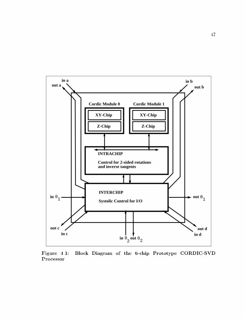
This architecture, shown in Figure 4.1, consists of four distinct modules that have
been implemented in four di�erent TinyChips. Two of the chips, the xy-chip and
the z-chip, together form one CORDIC module. Maximal parallelism is achieved
in the computation of the 2 � 2 SVD by including two CORDIC modules in the
processor. The control and interconnection for the SVD processor was implemented
in two separate chips. The intracontroller chip is used to provide all the internal
control necessary to implement the computation of the 2� 2 SVD. The systolic array
control is provided by the intercontroller chip. A hierarchical control mechanism
provides a way to e�ectively shield the low level control details from the higher level
controllers. At each level the controllers provide a set of macros to the controller next
in the hierarchy. In addition, this separation of control allows a degree of concurrency
not possible with a single controller. The next few sections describe the individual
chips in greater detail.
4.2.1 Design of the XY-Chip
Figure 3.6 on page 41 shows the basic blocks required in an implementation of a
�xed point CORDIC processor. The xy-chip implements the x and y data paths of a
single CORDIC module. Each path consists of a 16-bit register, a 16-bit barrel shifter
implementing all right shifts up to 15, a 16-bit ripple-carry adder with associated
temporary latches at the inputs, and a data switch to implement the cross-coupling
implied by the x and y CORDIC iterations (Equation 3.4 on page 16). Either CORDIC
iterations or scale factor correction iterations are possible on the data stored in the
registers. The absence of any on-chip control allows an external controller complete
exibility of the number of iterations as well as the nature of each iteration. Read and
write access to the x and y registers is possible independent of computation. Several

49
Figure 4.2: Die Photograph of the XY-Chip

50
versions of the xy-chip have been fabricated [7]. Figure 4.2 shows a die photograph
of the xy-chip.
4.2.2 Design of the Z-Chip
The z-chip complements the xy-chip to form a complete 16-bit �xed point implemen-
tation of the CORDIC module. It implements the z data path that consists of a 16-bit
z-register, a carry-lookahead adder and a ROM table of 16 angles. It also implements
a controller to provide all the control signals for the xy datapaths in the xy-chip and
the z datapath in the z-chip. This controller allows use of the CORDIC module in
�ve modes: Z-reduction, Y-reduction, scale factor correction, single add and subtract,
and divide-by-two. These are the only ALU operations required in the computation
of the SVD, which allowed �ne tuning the controller to perform these operations. The
design of this chip was completed by Szeto [33]. Figure 4.3 shows a die photograph
of the z-chip.
4.2.3 Design of the Intra-Chip
The intra-chip controls data movement between a register bank and two CORDIC
modules, and sequences the ALU primitives provided by the z-chip on the matrix
data to implement a 2� 2 SVD. It allows operation in three modes corresponding to
processor behavior in three di�erent positions in the array. If the processor is on the
main diagonal of the array, it computes the left and right angles and then uses these
angles to diagonalize a 2 � 2 submatrix. The processors P00, P11, P22 and P33 in
Figure 2.1 on page 9 are examples of such a processor. Any o�-diagonal processor only
transforms a 2� 2 submatrix with the angles received from the previous processors.
However, if a processor is diagonally a multiple of three away from the main diagonal,
for example processor P03, in addition to the transformation, a delay equal to the

51
Figure 4.3: Die Photograph of the Z-Chip

52
Tri-State Buffer
Shift Register
Register Bank
10Registers
Logical Zero
1616
16
16
Data Bus
Serial Datafrom Interchip
Serial Datato Interchip
Intra-Controller
CORDIC StartCORDIC DoneCORDIC OpcodeIntra StartIntra Done
Operation Code
Internal Controls
Figure 4.4: Block Diagram of the Intra-Chip

53
Figure 4.5: Die Photograph of the Intra-Chip

54
time it takes to compute the angles is included. The delay is necessary to maintain
synchronization between all the processors due to the wavefront nature of the array.
These three modes allow the same processor to be used in any position of the array
in spite of the required heterogeneity. The aforementioned storage is a register bank
consisting of ten registers implemented in the intra-chip. A 16-bit bus interconnects
these registers and the two CORDIC modules. A block diagram of the intra-chip is
shown in Figure 4.4. Figure 4.5 shows a die photograph of the intra-chip.
4.2.4 Design of the Inter-Chip
The inter-chip contains the controller that exercises the highest level of control in the
processor. As a communication agent, it implements the systolic array control for
the SVD processor. The parallel ordering data exchange [5], which provides a new
pair of data elements at the main diagonal to be annihilated, is implemented in this
chip. A set of six shift registers, as shown in Figure 4.6, is used as communication
bu�ers to store a copy of the data to be exchanged with the other processors while
the intra-chip operates concurrently on its own private copy of the data.
Interprocessor communication is through a set of eight serial links. Four of these
links are hardwired to exchange data with the diagonal neighbors. Four other links
serve to systolically propagate the left angles horizontally and the right angles ver-
tically. Since the SVD algorithm is compute bound, the bandwidth provided by the
serial links is su�cient for the data interchange. In addition, pin limitations prohibit
implementation of parallel ports to communicate with neighboring processors. Data
is exchanged synchronously between processors. Data is shifted out to the neighbor-
ing processor and simultaneously shifted in from it. Synchronization in the array is
of utmost importance since no other form of synchronization is provided. This is in
accordance with the de�nition of systolic arrays [21] that emphasizes exploiting the

55
Shift Register a
Shift Register b
Shift Register c
Shift Register d
Shift Register h
Shift Register v 1-to-2Decoder
1-to-2Decoder
1-to-2Decoder
1-to-2Decoder
1-to-2Decoder
1-to-2Decoder
2-to-1 MUX
2-to-1 MUX
2-to-1 MUX
2-to-1 MUX
2-to-1 MUX
2-to-1 MUXIn a
In b
In c
In d
In h
In v
Out a
Out b
Out c
Out d
Out h
Out v
Serial Datafrom Intra-Chip
Serial Datato Intra-Chip
INTER-CHIP Array Control Signals
Inter-ChipOperation Code
Figure 4.6: Block Diagram of Inter-Chip
special-purpose nature of the array to eliminate the overhead of synchronization. In
the prototype, pin limitations forced a serial link for communication of data with the
intra-chip. The inter-chip controller also allows initialization of the array by loading
the matrix data. The inter-chip was designed by Szeto [3] Figure 4.7 shows a die
photograph of the inter-chip.
4.3 The CORDIC Array Processor Element
The CORDIC array processor element (CAPE) is a single chip implementation of the
CORDIC SVD processor [17]. This chip incorporates elegant solutions to the problems
encountered in the six-chip prototype. CAPE also includes additional details necessary
to construct a working systolic array. CAPE essentially consists of the same basic cells

56
Figure 4.7: Die Photograph of the Inter-Chip

57
as the prototype. Many of the architectural enhancements were made to reduce the
communication required within the chip. A completely new loading scheme was added
to facilitate easy interface with a variety of hosts. The next few paragraphs describe
the details of all these improvements.
A study of the prototype CORDIC units indicated that better numerical accuracy
could be achieved with some modi�cations to the modules as described in Chapter 3.
To improve the numerical accuracy of the inverse tangent calculations, a normalization
shifter was included in each of the x and y data paths. These shifters are activated
during Y-reduction by two leading zero encoders that monitor the magnitude of the
x and y data. Simulations indicate that this scheme provides several extra bits of
accuracy in many cases.
The CORDIC modules in the prototype converge only for vectors in the �rst and
fourth quadrants while operating in the Y-reduction mode. The modi�ed scheme uses
the exclusive-or of the sign bits of the x and y registers to control the next iteration.
This e�ectively increases the range of convergence for the CORDIC modules. In
addition, the above scheme adds symmetry to the x and y data paths since they
cannot be distinguished externally. This allows the same CORDIC module to rotate a
vector in either clockwise or anticlockwise direction. Some data movement is rendered
unnecessary by the above method, for example, if the data to be used in the next
computation already resides in the x and y registers in the wrong order, since the
de�nition of the x and y registers can be interchanged, no data movement is required.
The z-chip was modi�ed to allow mapping the x, y and z registers as part of the
register bank. This allows reuse of the data left in the registers by a previous computa-
tion, which is important when attempting to cut down the communication overhead.
A study of the prototype SVD processor showed that there was a large overhead in-
curred in moving data to the appropriate registers between computations. A double

58
16
External Bus
Multiplexor Inter-Controller
Intra-Controller
Internal Bus0
Transceiver Transceiver
CORDICModule0Shifter 0
Shifter 1
Shifter 2
Reg 0
Reg 1
Reg 2
TransceiverTransceiverRegister Bank 0
Register Bank 1
Shifter Bank 0
Shifter Bank 1
SerialData In
SerialData Out
8
16
16
Internal Bus116
1616
16
6 6
CORDICModule1
Figure 4.8: Internal Architecture of CAPE
bus architecture, as shown in Figure 4.8, was used to minimize this communication.
A separate CORDIC module is hardwired to communicate on each bus. The set of
six registers is split into two banks that can communicate with either bus allowing
simultaneous access to two di�erent registers. The number of registers required in
the architecture was reduced from ten to six due to mapping of the CORDIC registers
as general purpose registers. The double bus allows concurrent data movement to
the two CORDIC modules, which reduces communication cycles by half. Using the
double bus architecture did not cause an increase in the area of the chip. This was a

59
result of the reduction in the size of the intra-chip controller to half its original size.
This corresponds to a reduction in the number of states due to greater concurrency
provided by the architecture.
Special cases that occur in the SVD computation require extra hardware. Two
zero comparators were included to detect the case tan�1(0=0). This is an invalid
computation on the CORDIC modules that return a code equivalent to the oating-
point NaN. The SVD algorithm allows such computed angles to be replaced by zero.
The zero comparators compare the data on the bus with zero and return a control
signal to the intra-chip controller to handle this special case. A literal constant zero
can be driven onto either bus and hence into any register. This allows forcing a
register to store a zero to handle special cases.
The inter-chip has been modi�ed to handle an improved array loading scheme. The
prototype did not make any special provision to e�ciently load the array. Since CAPE
is to be used in a systolic array in a real system, the interface with the host has been
re�ned. A parallel port has been included along with the requisite handshake signals.
The controller implements an asynchronous loading scheme that allows interfacing
with a host running at an independent clock rate.
The prototype inter-chip was pin limited and hence forced to communicate with
the intra-chip through a serial link. This restriction is no longer valid in the single
chip implementation. Consequently, this serial link was replaced with an internal
parallel bus that reduces the time to exchange data items between the intra-chip and
the inter-chip. The rest of the inter-chip was redesigned with only minor changes.

60
4.4 Issues in Loading the Array
Data loading is a key issue in the design of a systolic array. Systolic architectures
typically include data loading as part of the algorithm. Data is continually loaded
as new results are unloaded. A systolic loading scheme increases the throughput
of the array by pipelining several di�erent computations. An important problem
in the design of any pipeline is to keep the pipe full at all times, since it a�ects
the throughput. The time taken to �ll or empty a pipeline is analogous to the non-
parallelizable section of a program, which limits the speedup that can be achieved just
by increasing the number of processors [32]. In a systolic array, computation typically
begins in a subset of the processors and then propagates to other processors. The
goal of a loading scheme is to overlap communication and computation to the largest
degree possible by loading the processors in the order that the data is required.
In the SVD array, as illustrated by Figure 2.2 on page 11, computation starts at
the main diagonal and propagates as diagonal waves of activity towards the corners
of the array. Consequently, a systolic loading scheme should load the main diagonal
as early as possible and continue with the other super and sub-diagonals at a rate
that is not slower than the rate of computation. The computation of the SVD in the
array takes O(p log p) time, where each sweep takes O(p) time. Since all the array
data is required in one sweep, the loading algorithm has to be at least O(p). Since,
the matrix data itself does not propagate systolically as part of the SVD algorithm,
currently, the loading algorithm and the SVD algorithm are independent.
In a square array, it is necessary to load a total of O(p2) data elements. Thus
any O(p) loading algorithm requires O(p) entry points. Hence, it is not possible
to build a scalable SVD array with a constant number of entry points. This is not
a problem, however, in some real-time processing applications. Some applications

61
combine analog sensors with each processor, such that data is loaded directly from
the sensor to the processor, providing O(n2) entry points. In such an application,
loading is not a problem.
The simplest loading scheme involves loading the array a column at a time.
Assuming that the data is loaded from the left edge, the data for the right edge
is loaded �rst, and as new columns are loaded, the previous columns are systolically
propagated right. This is an O(p) loading algorithm. However, the main diagonal is
not loaded till the entire array has been loaded and hence does not allow any overlap
of communication with computation.
A systolic loading scheme that starts at the diagonal, needs to load the main
diagonal, followed by the next super and sub diagonals and so on. This scheme
requires each processor to know exactly where it is located in the array, so it can
propagate the correct number of elements to the right and left. The algorithm requires
O(p) time to load. However, this loading scheme requires a complex control to load
and unload the array. The main drawback is that it requires multiple parallel ports
in each processor, which is a problem due to pin limitations.
4.4.1 Data Loading in CAPE
In CAPE multiple buses are used to load the array (Figure 4.9) in time O(p). All
the processors on a row are connected by a bus. Only one processor is enabled
permanently, while the others are daisy-chained. After loading an appropriate number
of words, the currently enabled processor enables the next processor in the chain. The
array consists of p=2 entry points, one at each of the diagonal processors. The host
has to provide the data in the correct order, which depends on how the processors
have been chained.

62
CORDIC Systolic Processor Array (CSPA)
CAPECAPECAPECAPE
CAPE CAPE CAPE CAPE
CAPECAPE CAPE CAPE
CAPE CAPE CAPE CAPEDSP 1
DSP 2
DSP 3
DSP 4
8
8
8
8
Figure 4.9: A square array of CAPE chips connected to a host, a linear
array of DSP processors, for Robotics

63
In large arrays global connections will limit the clock rate due to long paths.
This problem has been avoided in CAPE by using an asynchronous handshake to
load data into the processors. This decouples the speed of loading from the speed of
computation. The array can run at a clock independent of the speed at which the
array can be loaded. Since the processors have a �xed latency to acknowledge, it is
possible to load the diagonal processor and start computation before the entire array
has been loaded. Asynchronous loading allows the array to be interfaced with a host
running at an independent clock speed. For very large arrays, the speed at which the
array can be loaded reduces. When such a limit is reached, the speed of computation
can be decreased to achieve a graceful degradation as the size of the array increases.
This chapter described the design of the CORDIC-SVD processor. Several en-
hancements can be made to the SVD array, with minor modi�cations to the design
of the processor. Some of these alternative array designs are described in the next
chapter.

Chapter 5
Architectures to Improve Processor Utilization
5.1 Introduction
In a system with a large number of processors, keeping them busy at all times presents
a formidable task, leading to intervals when processors wait for some other event to
occur in the system. Sometimes, however, this idle time can be used for tasks nor-
mally regarded as overhead. An example of this is the fault-tolerance recon�guration
scheme [9] proposed by Cavallaro, where the idle processors backup the functionality
of a neighboring faulty processor. Use of this time for fault-detection is yet another
example. However, if a higher throughput is desired, it would be possible to reduce
the idle time by pipelining several di�erent computations. Idle time is of concern in
the CORDIC-SVD array, since at any given time two-thirds of the processors are idle.
This chapter focuses on methods to eliminate the idle time or to utilize it to
perform some useful computations. An array, in which the angles from the diagonal
processors are broadcast along a row or column, can attain a speedup close to 100%
over the current design. A variation of this scheme that avoids the broadcast and yet
achieves the same speedup is discussed in Section 5.3. This architecture can be useful
to achieve a higher throughput if only the singular values need to be computed by
the array.
Many applications require the complete SVD decomposition including the left and
the right singular vectors. A modi�cation to the current array design allows the
64

65
complete decomposition to be computed in the same time that it takes to compute
the singular values. The impact of this algorithm on the design of the processor is
discussed in Section 5.4.
A systolic array, by de�nition, does not require any globally synchronous control
signals, except perhaps the clock. Many arrays require a globally connected start sig-
nal to achieve synchronization between a large subset of the processors. Section 5.2
discusses an architectural alternative that avoids such a signal, allowing greater scal-
ability.
5.2 Architecture for Systolic Starting
The CORDIC-SVD processor has been designed assuming a global start signal to syn-
chronize all the processors on the main diagonal. This type of a signal is omnipresent
in most systolic array designs to facilitate easy understanding of the timing issues in
the array. In most arrays, the processors retain a certain degree of simplicity that
allows elimination of these signals by skewing the computations among processors,
after the initial design phase. The SVD processor is no exception and lends itself to
this sort of skewing, permitting a system start signal that has a constant fan-out in-
dependent of the size of the array. A start to the diagonal processor P00 in Figure 5.1
is propagated diagonally, with a clock cycle delay at each processor. Consequently,
the diagonal processors are no longer in unison. This a�ects the timing requirements
of the rest of the array. Special care is required while interconnecting the control and
data-paths of the various processors, which were hitherto relatively easy to compre-
hend. Delays have to be inserted at the appropriate places to solve timing problems.
Figure 5.1 and 5.2 show an interconnection for the CORDIC-SVD processor that
results in a consistent operation. The most important modi�cation made to the SVD

66
S
D
W1
W2
S
D W1
W2
S
W1
W2
S
W1 W2
S
D W1
W2
S
D
W1
W2S
D
W1
W2
S
DW1
W2
S
W1
W2 SD
W1W2
S
W1
W2
S
D
W2
S D
W2SD
W1W2
SD
W1W2
S
D
W1 W2
D
D
D
D
D D
D
D
D
D D
D
D D
D
D1
D1
W1
D1
W1D
D1D1
S : StartW1: Wait1W2: Wait2D: CalcdoneD1: Calcdone Delayed by One clock cycle
Start
P00 P00 P00 P00
P00 P00 P00 P00
P00 P00 P00 P00
P00 P00 P00 P00
Logic 1
Logic 1
Figure 5.1: Interconnection of Control Signals for Systolic Starting

67
A B
C D
θ LD
θRD
θR
θR
θR
θR
θ L θ Lθ L
θ Lθ Lθ Lθ Lθ Lθ L
A B
C D
A B
C D
A B
C D
A B
C D
A B
C D
A B
C D
A B
C D
A B
C D
A B
C D
A B
C D
A B
C D
A B
C D
A B
C D
A B
C D
A B
C D
P00 P01 P02 P03
P10 P11 P12 P13
P20 P21 P22 P23
P30 P31 P32 P33
θ LD θ LD
θRD
θRD
θR
θR
θ LD θ LD
θRD
θRθ
RDθ
RD
θR
θR
θR
θR θ
Rθ
Rθ
R
θ LD θ Lθ Lθ L
θ Lθ L
θ L θ Lθ L θ L
θR
θR
θRθ
R
θ LDθ Lθ
Rθ
RD
: Left angle receive or transmit
: Delayed left angle transmit
: Right angle receive or transmit
: Delayed right angle transmit
Figure 5.2: Interconnection of Data Lines for Systolic Starting

68
processor is the introduction of a clock cycle delay in a few selected signals and data
links. In addition to a normal done signal, a signal delayed by one clock cycle, called
the delayed done, is required to maintain coherence at the right and bottom edges
of the array. Angle transmission from the diagonal processors to the east and west
neighbors is skewed. The angle transmitted east is delayed one clock cycle to account
for the skew in the computation along the diagonal. Such a delay is not required
in the angle transmitted west . A similar delay is required in the angle transmitted
south but not in the angle transmitted north. The only other change required in
the processor is to delay the exchange of data with the south-east processor by one
cycle. All other control signals and data exchanges in the current design remain
unmodi�ed. An interconnection of these modi�ed processors, as shown in Figure 5.1
and 5.2, achieves the goal of eliminating the global start signal. Modi�cation of the
above scheme to eliminate global signals in other arrays requires a careful study of
the timing dependencies, but, is nevertheless straightforward.
Figure 5.3 shows snapshots of array taken at various time instants and helps il-
lustrate the inner working of the array. The processors that are highlighted, are the
processors which are computing at the given time instant. The highlighted commu-
nication links indicate an exchange of data during that cycle. The communication
is assumed to take only one clock cycle for simplicity, but the analysis can easily be
extended for more cycles. Some of the salient features of this �gure are:
� The start signal to processors P00 is provided at time instant t1. This signal is
propagated systolically down the diagonal resulting in processors P00, P11, P22,
P33 starting computations at time t1+1, t1+2, t1+3 and t1+4 respectively.
� Processor P00 completes its computations at time t2. However, it delays
the transmission of the angles to processors P01 and P10 by one clock cycle.

69
Time Step: t1 Time Step: t1+1 Time Step: t1+2
Time Step: t1+3Time Step: t2Time Step: t2+1
Time Step: t2+2 Time Step: t2+3 Time Step: t2+4
Time Step: t3Time Step: t3+1Time Step: t3+2
Figure 5.3: Snapshots of a Systolic Starting scheme

70
Processor P11 stops computing at time t2+1 and immediately starts sending
out the angles to processors P01 and P10 completing the rendezvous of the
left and right angles at the processors P01 and P10. The same sequence of
operations continues all along the diagonal. Thus processors P01, P10, P21,
P12, P32, P23 start computing at time t2+2, t2+2, t2+3, t2+3, t2+4, t2+4,
respectively.
� Processors P01 and P10 �nish �rst at t3. The diagonal processor P00 on receiv-
ing the wait1 signal, exchanges matrix element a, but delays exchanging data
element d by one clock cycle. This allows it to synchronize with processor P11,
which receives its wait1 at t3+1 and shifts out its matrix data element a, which
it exchanges with the data element d of processor P00. The same sequence
continues down the diagonal.
Using a systolic starting scheme requires an extra n=2 clock cycles to �nish, as com-
pared to the scheme with global start . The extra cycles form an insigni�cant portion
of the total time, 0.02% for an 8� 8 matrix, and hence do not a�ect the performance
of the array.
5.3 Architecture for fast SVD
Many applications utilizing the SVD require only the singular values of a matrix.
Often, some parameter of the matrix, like the 2-norm or the Frobenius-norm [15],
is desired and can be evaluated from the knowledge of the singular values alone.
Rank determination and condition estimation problems, too, require only the singular
values. Hence, a speedup in the computation of the singular values alone, can be useful
in such applications.
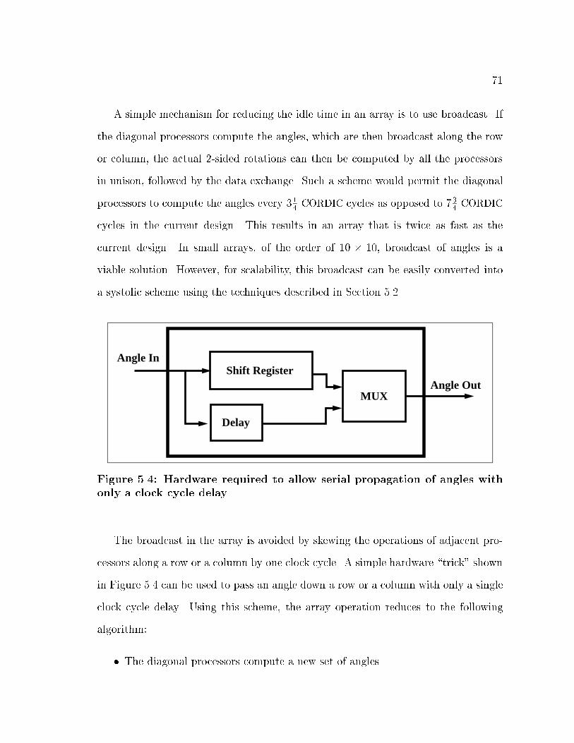
71
A simple mechanism for reducing the idle time in an array is to use broadcast. If
the diagonal processors compute the angles, which are then broadcast along the row
or column, the actual 2-sided rotations can then be computed by all the processors
in unison, followed by the data exchange. Such a scheme would permit the diagonal
processors to compute the angles every 314CORDIC cycles as opposed to 73
4CORDIC
cycles in the current design. This results in an array that is twice as fast as the
current design. In small arrays, of the order of 10 � 10, broadcast of angles is a
viable solution. However, for scalability, this broadcast can be easily converted into
a systolic scheme using the techniques described in Section 5.2.
Shift Register
Delay
MUX
Angle In
Angle Out
Figure 5.4: Hardware required to allow serial propagation of angles with
only a clock cycle delay
The broadcast in the array is avoided by skewing the operations of adjacent pro-
cessors along a row or a column by one clock cycle. A simple hardware \trick" shown
in Figure 5.4 can be used to pass an angle down a row or a column with only a single
clock cycle delay. Using this scheme, the array operation reduces to the following
algorithm:
� The diagonal processors compute a new set of angles.

72
� The angles are propagated down the rows and columns with only a clock cycle
delay between the angles received by adjacent processors. Thus every processor
mimics the operation of the previous processor with a single clock cycle delay.
� After a processor �nishes receiving the angles, it starts the 2-sided rotation.
Thus all the processors compute the 2-sided rotation with a single clock cycle
delay. This constant delay allows elimination of the wait1 and wait2 signals.
In CAPE, the control signals, wait1 and wait2 , indicate the end of computation
one diagonal and two diagonals away, respectively.
� Every processor that completes a rotation can start data exchange with the
following rules:
{ After one clock cycle delay, the processor can begin exchange of data,
which it should on receiving wait1 ,
{ After two clock cycles delay, the processor can begin exchange of data,
which it should on receiving wait2 .
� After the data exchange the entire process is started again.
A systolic starting scheme as described in the previous section can be used to eliminate
the global start signal. This introduces additional skews in the array. Special care
is required when exchanging data at the boundaries of the array. An extra bit of
information is required by every processor to determine if it is on the boundary.

73
5.4 Architecture for Collection of U and V Matrices
Major Cycle 1 Major Cycle 2 Major Cycle 3
Major Cycle 4Major Cycle 5Major Cycle 6
Σ
Σ
Σ
Σ
U
U
U
U
V
V
V
V
Σ
Σ
Σ
Σ
U
U
U
U
V
V
V
V
Σ
Σ
Σ
Σ
Σ
Σ
Σ
Σ
Σ
Σ
U
U
U
U
U
U
Σ
Σ
Σ
Σ
Σ
Σ
Σ
Σ
U
U
U
U
V
V
V
V
V
V
V
V
V
V
U
U
U
U
U
U
U
U
Σ
Σ
Σ
Σ
V
V
Figure 5.5: Snapshots of an Array Computing U and V
In spite of the assertions made in Section 5.3, many applications do require the
computation of the left and right singular vectors for further processing. An example
of such an application is the inverse kinematics engine for a robot, the RICE-OBOT
1, which relies on the singular values and the vectors for singularity avoidance. A
rather surprising result obtained while studying ways to utilize the idle time is that
it is possible to compute the U and V matrices along with the singular values in the
same array in about the same time that it takes to compute the singular values alone.
The Jacobi algorithm for computing the SVD applies a sequence of left and right
orthogonal transformations to the original matrix to diagonalize it. The product of the
left transformations is the �nal U shown in equation 2.5. Similarly, the product of all
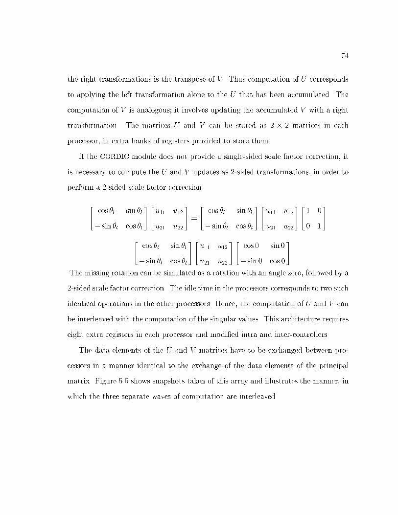
74
the right transformations is the transpose of V . Thus computation of U corresponds
to applying the left transformation alone to the U that has been accumulated. The
computation of V is analogous; it involves updating the accumulated V with a right
transformation. The matrices U and V can be stored as 2 � 2 matrices in each
processor, in extra banks of registers provided to store them.
If the CORDIC module does not provide a single-sided scale factor correction, it
is necessary to compute the U and V updates as 2-sided transformations, in order to
perform a 2-sided scale factor correction.
24 cos �l sin �l
� sin �l cos �l
3524 u11 u12
u21 u22
35 =
24 cos �l sin �l
� sin �l cos �l
3524 u11 u12
u21 u22
3524 1 0
0 1
35
=
24 cos �l sin �l
� sin �l cos �l
3524 u11 u12
u21 u22
3524 cos 0 sin 0
� sin 0 cos 0
35
The missing rotation can be simulated as a rotation with an angle zero, followed by a
2-sided scale factor correction. The idle time in the processors corresponds to two such
identical operations in the other processors. Hence, the computation of U and V can
be interleaved with the computation of the singular values. This architecture requires
eight extra registers in each processor and modi�ed intra and inter-controllers.
The data elements of the U and V matrices have to be exchanged between pro-
cessors in a manner identical to the exchange of the data elements of the principal
matrix. Figure 5.5 shows snapshots taken of this array and illustrates the manner, in
which the three separate waves of computation are interleaved.
Chapter 6
VLSI Implementation Issues
6.1 Design Methodology
A structured VLSI design approach following the Mead and Conway methodology [27,
37] was used in the design of all the chips for the CORDIC-SVD processor. Static
complementary (CMOS) logic was used to simplify design. In addition, a formal two-
phase clocking strategy was imposed [19, 20] to allow proper functionality independent
of the propagation delays.
All the chips comprising the prototype were developed using the Magic [29] layout
editor and other VLSI tools from the University of California, Berkeley. Magic allows
a hierarchical design, which facilitates layout in a a bit-slice manner. Programmable
Logic Arrays (PLAs), used as controllers, were generated automatically from a high
level description. All the other cells were custom designed. Magic provides limited
routing facilities, which are su�cient for small chips. A large chip like CAPE, however,
cannot utilize this facility. The amount of custom design involved in this approach
makes design using Magic a time consuming operation.
The term Silicon Compilation has been coined for high level CAD tools that allow
generation of VLSI chips almost completely from a high-level description, like VHDL.
An alternate set of CAD programs, Octtools, allows this kind of a design. Octtools
[31] take an object-oriented approach to VLSI design. This allows extensive functional
simulation of an unplaced, unrouted chip, generated from a high level description.
75
76
Actual placement and routing of the chip can be postponed until the description
is completely debugged. The di�erent modules are generated from the high-level
description of the cells, using libraries of standard elementary cells. A placement
tool, based on the simulated annealing technique, �nds an optimal placement of the
modules to minimize a variety of costs, like wire length and chip area. Finally, a
routing package physically routes these cells. Additional post-processing steps reduce
the number of vias and compact the layout to satisfy the minimum spacing rules.
Design using these tools can reduce the tedium of VLSI design considerably.
The single chip, CAPE, utilized the advanced placement and routing features pro-
vided by Octtools. Most of the modules were scavenged from the original prototype,
and modi�ed to improve performance, using the Magic editor. These modules were
then converted to Octtools format to place and route the �nal chip. This routed chip
was then converted back to Magic format for �nal placement and routing of the pads.
Functional simulation was performed using the switch-level simulators esim and
irsim. Longest path delays were identi�ed with crystal. Detailed simulation at the
circuit level was performed for critical cells using spice. The circuit design of some of
the cells was modi�ed to allow functional simulation using the switch-level simulators.
For instance, an extra inverter was included to bu�er the output of each latch to
prevent back-propagation and allow functional simulation. This simulation is essential
to eliminate any design errors, since fabrication is a costly process.
The six-chip prototype was designed as four TinyChips, fabricated on 2200�2200�die using a 2� CMOS n-well process. The transistor count for the di�erent chips varied
between 4500 and 6000 transistors. The single chip version, CAPE, was designed on a
6900� 5600� die and contained about 26000 transistors. A plot of this chip is shown
in Figure 6.1.

77
Figure 6.1: Plot of the completed Single Chip Implementation

78
6.2 Reducing Skews in Control Signals
The modules that constitute the chip, when described at the circuit level, require the
logical complement of most of the control signals along with the original signals. Some
signals, for instance the clock signals, have a heavy resistive and capacitive (RC) load
on the signal lines, due to the large number of cells that require them. Hence the
structures required to drive these signals require careful design to prevent large skews
between the signals and their complements, which can cause incorrect operation. A
circuit as shown in Figure 6.2, which consists of two inverters in tandem, can cause
a large skew between the transitions of the signal and its complement. The large RC
load results in a large switching time that a�ects the input of the second stage, which
itself is heavily loaded, thus, resulting in a large skew. An alternate design as shown
in Figure 6.3 avoids this situation by controlling the skew between the inputs of two
inverters, which generate the signal and its complement. An additional inverter is
required to invert one of these input signals. However, this inverter is connected to
the input of only one inverter, resulting in a fast switching. Thus the skew in the
inputs of the drivers is small. Assuming a large, but nearly equal, load on the signal
and its complement, the �nal skews will be small. Static CMOS design, by de�nition,
requires every structure to be associated with an identical complementary structure.
clock (Large Load)
clockbar (Large Load)
clockin
Figure 6.2: Generation of the
heavily loaded clock and its com-
plement results in a large skew
clockbar(Large Load)
clock (Large Load)
(Small Load)
clockin
Figure 6.3: Generation of the
heavily loaded clock and its com-
plement results in a small skew

79
Though this nearly doubles the transistor count, it leads to a more symmetrical design
that can be compact. It also leads to the desirable property of an almost identical
RC load on any signal and its complement.
Circuits that need to drive a large load can be designed with wider transistors.
This causes the transistors to switch faster since the resistance is reduced by a factor
that is greater than the increase in the capacitance. This is true only up to a certain
maximum size, after which the propagation delay increases again. These techniques
were used to reduce the skews of numerous control signals.
6.3 Design of an Adder
To obtain a simple design with minimal area complexity, ripple carry adders were
used in the CORDIC units. However, a poorly designed adder can result in a large
propagation delay, a�ecting the overall clock rate. The adder used in the prototype
chips was modi�ed to reduce this propagation delay when used in CAPE.
In a ripple carry adder, the longest path occurs from the carry-in of the adder
to the carry-out. Reducing the delay from one stage of the adder to the next can
signi�cantly improve the speed of operation of the adder. To reduce the propagation
delay of the carry through a single stage, the minimum number of levels of logic should
be used to generate the carry-out of that stage. Using wider transistors can further
reduce this delay. Since PMOS transistors are twice as slow as NMOS, the logic should
be designed to contain the minimal number of PMOS transistors in series. Reducing
the load seen by the carry-out from a previous stage can further reduce propagation
delay. This reduction can be e�ected by using pseudo-NMOS logic. The use of pseudo-
NMOS logic increases power dissipation, but this is negligible compared to the power
80
dissipation of the entire chip. The longest delay in the adder used in CAPE was
reduced by half by using these techniques.
6.4 Testing
PC-based high speed test equipment, Omnilab from Orion Instruments [28], was used
in verifying operation of the chips. This tester allows testing up to a frequency of 17
MHz, which corresponds to a clock frequency of 4.25 MHz for the chip, due to the
two-phase clocking strategy. All the six chips, which constitute the SVD processor,
operate at the maximum test frequency.
Verifying correct functionality of the sub-units of the SVD processor was the pri-
mary goal of the testing process. The chips were tested with the same vectors, which
were used for simulation. The testing exposed several errors in the design of the pro-
totype. Table 6.1 lists the most signi�cant of these errors. The errors are categorized
as design errors or architecture problems. The design errors occurred due to the in-
dependent design of the various units. These were primarily errors in the interaction
between di�erent units, which could be veri�ed only after fabrication. The architec-
ture problems, on the other hand, required further research to determine a low-cost
solution. The numerical accuracy problem encountered in Y-reduction belongs to the
latter class of problems. The error observed in practice was larger than expected and
required the detailed analysis described in Chapter 3. The analysis indicated that
normalization could solve the accuracy problem.
A C-language library of routines was created to use the CORDIC module as a
co-processor for an IBM PC. A parallel I/O card on an IBM PC-AT was used to
communicate with the CORDIC processor. The design of the prototype requires ini-
tial matrix data to be loaded synchronously. After an initial start signal, a di�erent

81
Design Errors
Width of the Z-Datapath Two bits are required before the binary point inorder to represent all angles from ��=2 to �=2.The representation of the angles stored in theROM had to be changed accordingly.
Calculation of angles From equations 2.8, the sum and di�erence of theleft and right angles is obtained. The computationof �l and �r can be executed in the following order:
1. Compute (�l+�r) and (�l-�r)
2. Compute (�l + �r)=2 and (�l � �r)=2)
3. Compute �l and �r
In the prototype the shift was performed after 2�land 2�r were computed from the sum and the dif-ference, resulting in an over ow if the numbersare too large. This e�ectively reduced the rangeof all angles to ��=4 to �=4. This problem wascorrected in the single chip.
Architectural Problems
Convergence of Y-reduction Negative values of x0 prevent the Y-reduction it-erations from converging. A di�erent choice of �isforces convergence.
Accuracy A careful study was necessary to determine thenumber of signi�cant bits that could be guaran-teed by the processor. The error analysis is de-scribed in Chapter 3.
Computation of tan�1 (0=0) A careful examination of the SVD algorithm indi-cates that this problem can be corrected by replac-ing the angle with a zero angle. Zero comparatorswere used to detect this condition and correct it.
Table 6.1: A list of some of the problems in the 6-chip prototype

82
data element is expected on the bus on each successive clock cycle. This prohibits
generation of the processor clock from the PC clock. The solution to the clock gen-
eration problem in the prototype was to generate the clock using the parallel ports.
The program generates a clock for the processor by treating it as a control signal,
requiring four separate writes to the parallel port for each clock cycle. This interface
was helpful in performing an exhaustive test of the CORDIC processor. A program,
which performs a simulation of the CORDIC module at the bit-level, was written to
generate the expected results for the exhaustive tests. Discrepancies in the outputs
were used to determine design errors.
Data loading in CAPE was modi�ed to be asynchronous, solving the interface
problem by allowing the array to operate at a rate independent of the PC clock.
Asynchrony, however, introduces an additional problem. In an asynchronous system,
a data transition at the same instant as a clock transition can result in metastability .
In such a state the output voltages remain unde�ned for a prolonged period of time.
One solution to the metastability problem is to design ip- ops that are resilient
to this problem [22]. The same e�ect can be achieved externally. Typically, the
TTL MSI ip ops in the F-series have a very small metastability window and hence
decrease the probability of the occurrence of the problem. Using more of these chips
in series can further reduce this probability. The latter approach was preferred in
CAPE due to its simplicity.
Study of the prototype helped identify those factors that a�ect performance. Com-
munication within the chip was identi�ed as the main source of overhead. The extra
clock cycles associated with this communication were eliminated in the single chip im-
plementation by using an enhanced architecture. These enhancements were described
in Chapter 4. Table 6.2 shows a breakdown of the various communication costs in a
single computation cycle. A computation cycle in the table corresponds to the time
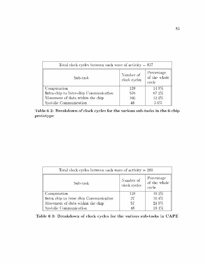
83
Total clock cycles between each wave of activity = 857
Sub-taskNumber ofclock cycles
Percentageof the wholecycle
Computation 128 14.9%Intra-chip to Inter-chip Communication 576 67.2%Movement of data within the chip 105 12.2%Systolic Communication 48 5.6%
Table 6.2: Breakdown of clock cycles for the various sub-tasks in the 6-chip
prototype
Total clock cycles between each wave of activity = 260
Sub-taskNumber ofclock cycles
Percentageof the wholecycle
Computation 128 49.2%Intra-chip to Inter-chip Communication 27 10.4%Movement of data within the chip 57 21.9%Systolic Communication 48 18.4%
Table 6.3: Breakdown of clock cycles for the various sub-tasks in CAPE
84
required by three consecutive diagonals to complete computation. In the prototype,
the principal communication cost was due to an unavoidable serial link connecting the
intra-chip and inter-chip. This cost was reduced to a small fraction in the single chip
design through the use of a parallel bus. Reducing inter-processor communication
would require use of parallel ports to transmit data between processors. However,
use of parallel ports in CAPE is not currently feasible due to pin limitations. The
internal communication, however, was reduced to half through the use of a double
bus architecture as described in Chapter 4.

Chapter 7
Conclusions
7.1 Summary
This thesis presented the issues involved in the VLSI implementation of a systolic
array to compute the SVD of a matrix, using CORDIC arithmetic techniques. Imple-
mentation of the CORDIC-SVD processor was carried out in two phases. Initially, a
prototype of the processor, composed of 6 chips, was developed. This required the
design of four custom MOSIS TinyChips. Testing of this prototype revealed several
architectural problems. Elegant solutions to all these problems, which were presented
in this thesis, were incorporated in CAPE, the single chip implementation.
The primary factor, which a�ected performance of the processor was the large
overhead incurred in moving data between the modules within the chip. In CAPE,
several changes were made to reduce this communication overhead. Since the CORDIC
modules in the 6-chip prototype used dedicated registers to operate, there was a need
to move the data to these registers for all arithmetic operations. In CAPE, these
registers were made part of the register set, eliminating the intermediate communi-
cation step when data had to be moved from a general register to these dedicated
registers. Another architectural improvement was a two-bus architecture, which was
developed to reduce the communication by half. Additional modi�cations helped to
further reduce the communication.
85

86
Another important problem encountered in the prototype was numerical accuracy
of the �xed-point CORDIC modules. Previous analyses of CORDIC neglected the
interaction between the x, y iterations and the z iterations. Consequently, the e�ects
of unnormalized x0 and y0 on the results of Y-reduction were not noticed. This
thesis presented a methodology to perform a detailed analysis of numerical error in
any mode of CORDIC. Examples which determine pessimistic bounds for Z-reduction
and Y-reduction were also presented. Although a bound on the error was found for
Z-reduction, no such bound could be found for Y-reduction. The analysis, however,
showed that a normalization of the initial values for Y-reduction was required to force
such a bound. A normalization scheme with low time penalty requires O(n2) area
to implement using conventional techniques. This area was reduced to O(n1:5) by
performing the overall shift as small shifts, which are implemented as part of the
CORDIC iterations. A detailed analysis of this novel method, which reduces the area
complexity with no associated time penalty, was presented in this thesis.
Several improvements and new features were developed, which can be incorporated
with small changes to the current processor design. A systolic starting scheme was
developed to eliminate a global start signal. This scheme allows greater scalability
and presents a method that can be used to achieve the same e�ect in other systolic
arrays. An architecture, which results in a speedup of 100% over the current design
was also developed. This scheme provides a way to achieve the performance gain
obtained through broadcast, without the global connections that prevent scalability.
The performance gain is achieved by eliminating idle time in the array. An alternate
scheme to utilize the idle time in the array was also developed. This scheme pipelines
the computation of the U and V matrices along with the singular values, to compute
all the three matrices in the time it currently takes to compute the SVD alone.

87
7.2 Future Work
The error analysis of �xed-point CORDIC indicates that oating-point CORDIC would
provide better numerical accuracy, since the normalization is already a part of oat-
ing-point arithmetic. Future implementations of CORDIC using oating-point units
can achieve better numerical accuracy.
Most commercial chips implement a Test Access Port (TAP) to provide observ-
ability and controllability during manufacturing testing. A similar TAP is often used
on printed circuit boards. IEEE standard 1149.1 de�nes the TAP protocol. It appears
that an approach similar to TAP can be used to implement run time fault detection.
Adherence to a standard would allow circuits with di�erent types of components
to interact and cooperate to detect faults in the system. Designing a complete sys-
tolic array that incorporates fault-tolerance can provide some insight to implementing
fault-tolerance in general-purpose systems.
Since the SVD array requires O(p2) processors, large arrays would bene�t from
higher levels of integration. Wafer-Scale Integration can provide the desired degree
of integration. A problem that requires further study is the design of the array as
an interconnection of modules, where each module is composed of several processors.
The number of pins on a wafer package limit the number of interconnections between
these modules.
Currently, WSI technologies require special post-processing steps, like laser repair,
to disconnect the faulty processors on the wafer. Fault tolerance techniques developed
for arrays of this nature can be used in WSI to eliminate the post-processing.
Bibliography
[1] H. M. Ahmed. Signal Processing Algorithms and Architectures. PhD thesis,
Dept. of Electrical Engineering, Stanford Univ., Stanford, CA, June 1982.
[2] H. C. Andrews and C. L. Patterson. Singular Value Decompositions and Digital
Image Processing. IEEE Trans. Acoustics, Speech, and Signal Processing, ASSP-
24(1):26{53, February 1976.
[3] J. Barnaby, B. On, and P. Szeto. A Systolic I/O Controller for the CORDIC-SVD
Processor. Technical Report ELEC 560, Rice University, December 1989.
[4] R. P. Brent and F. T. Luk. The Solution of Singular Value Problems Using
Systolic Arrays. Proc. SPIE Real-Time Signal Processing, 495(VII):7{12, August
1984.
[5] R. P. Brent, F. T. Luk, and C. F. Van Loan. Computation of the Singular
Value Decomposition Using Mesh-Connected Processors. Journal of VLSI and
Computer Systems, 1(3):242{270, 1985.
[6] J. R. Cavallaro. VLSI CORDIC Processor Architectures for the Singular Value
Decomposition. PhD thesis, School of Electrical Engineering, Cornell Univ.,
Ithaca, NY, August 1988.
[7] J. R. Cavallaro, M. P. Keleher, R. H. Price, and G. S. Thomas. VLSI
Implementation of a CORDIC SVD Processor. Proc. 8th Biennial Univer-
88

89
sity/Government/Industry Microelectronics Symposium, pages 256{260, June
1989.
[8] J. R. Cavallaro and F. T. Luk. CORDIC Arithmetic for an SVD Processor.
Journal of Parallel and Distributed Computing, 5(3):271{290, June 1988.
[9] J. R. Cavallaro, C. D. Near, and M. �U. Uyar. Fault-Tolerant VLSI Processor Ar-
ray for the SVD. IEEE Int. Conf. on Computer Design, pages 176{180, October
1989.
[10] D. Daggett. Decimal-Binary Conversions in CORDIC. IRE Transactions on
Electronic Computers, EC-8(3):335{339, Sept. 1959.
[11] J. M. Delosme. VLSI Implementation of Rotations in Pseudo-Euclidean Spaces.
IEEE Int. Conf. Acoustics, Speech and Signal Processing, 2:927{930, April 1983.
[12] J. J. Dongarra, C. B. Moler, J. R. Bunch, and G. W. Stewart. Chapter 11:
The Singular Value Decomposition. In Linpack Users' Guide, pages 11.1{11.23.
SIAM, Philadelphia, PA, 1979.
[13] R. A. Duryea. Finite Precision Arithmetic in Singular Value Decomposition
Processors. PhD thesis, School of Electrical Engineering, Cornell Univ., Ithaca,
NY, August 1987.
[14] G. E. Forsythe and P. Henrici. The Cyclic Jacobi Method for Computing the
Principal Values of a Complex Matrix. Transactions of the American Mathemat-
ical Society, 94(1):1{23, January 1960.
[15] G. H. Golub and C. F. Van Loan. Matrix Computations, Second Edition. Johns
Hopkins Univ. Press, Baltimore, MD, 1989.

90
[16] G. L. Haviland and A. A. Tuszynski. A CORDIC Arithmetic Processor Chip.
IEEE Trans. Computers, C-29(2):68{79, Feb. 1980.
[17] N. D. Hemkumar, K. Kota, and J. R. Cavallaro. CAPE-VLSI Implementation
of a Systolic Processor Array: Architecture, Design and Testing. In Ninth Bi-
ennial University/Government/Industry Microelectronics Symposium, June 1991
(to appear).
[18] S. L. Johnsson and V. Krishnaswamy. Floating-Point CORDIC. Technical Re-
port YALEU/DCS/RR-473, Dept. of Computer Science, Yale Univ., New Haven,
CT, April 1986.
[19] K. Karplus. Exclusion Constraints, A New Application of Graph Algorithms
To VLSI Design. Advanced Research in VLSI, Proc. 4th MIT Conference, pages
123{139, April 1986.
[20] K. Karplus. A Formal Model for MOS Clocking Disciplines. Technical Report
TR 84-632, Dept. of Computer Science, Cornell Univ., Ithaca, NY, August 1984.
[21] H. T. Kung. Why Systolic Architectures? IEEE Computer, 15(1):37{46, January
1982.
[22] Lee-Sup Kim and Robert W. Dutton. Metastability of CMOS Latch/Flip-Flop.
IEEE Journal of Solid-State Circuits, 25(4):942{951, August 1990.
[23] F. T. Luk. Architectures for Computing Eigenvalues and SVDs. Proc. SPIE
Highly Parallel Signal Processing Architectures, 614.
[24] F. T. Luk. A Parallel Method for Computing the Generalized Singular Value
Decomposition. Journal of Parallel and Distributed Computing, 2:250{260, 1985.

91
[25] F. T. Luk. A Triangular Processor Array for Computing Singular Values. Journal
of Linear Algebra and Its Applications, 77:259{273, 1986.
[26] F. T. Luk. Computing the Singular Value Decomposition on the ILLIAC IV.
ACM Transactions on Mathematical Software, 6(4):524{539, December 1980.
[27] C. A. Mead and L. A. Conway. Introduction to VLSI Systems. Addison-Wesley,
Reading, MA, 1980.
[28] Orion Instruments. The OmniLabTM User's Manual. Menlo Park, CA, June
1990.
[29] J. K. Ousterhout, G. T. Hamachi, R. N. Mayo, W. S. Scott, and G. S. Taylor.
Magic, a VLSI Layout System. ACM/IEEE 21st Design Automation Conference,
pages 152{159, June 1984.
[30] L. H. Sibul. Application of Singular Value Decomposition to Adaptive Beamform-
ing. IEEE Int. Conf. Acoustics, Speech, and Signal Processing, 2:33.11.1{33.11.4,
March 1984.
[31] R. Spickelmier. Octtools Distribution, Release 4.0. ERL/UC Berkeley Memoran-
dum, August 1990.
[32] H. S. Stone. High-Performance Computer Architecture. Addison-Wesley, July
1989.
[33] P. Szeto. Design of a Z-controller for the CORDIC-SVD Processor. Technical
Report ELEC 590, Rice University, May 1990.
[34] J. D. Ullman. Computational Aspects of VLSI. Computer Science Press,
Rockville, MD, 1984.

92
[35] J. Volder. The CORDIC Trigonometric Computing Technique. IRE Trans.
Electronic Computers, EC-8(3):330{334, Sept. 1959.
[36] J. S. Walther. A Uni�ed Algorithm for Elementary Functions. AFIPS Spring
Joint Computer Conf., pages 379{385, 1971.
[37] N. H. E. Weste and K. Eshraghian. Principles of CMOS VLSI Design. Addison-
Wesley Publishing Company, Reading, MA, 1985.
[38] B. Yang and J. F. B�ohme. Reducing the computations of the SVD array given
by Brent and Luk. SPIE Advanced Algorithms and Architectures for Signal
Processing, 1152:92{102, 1989.